US10504777B2 - Method of manufacturing wafer level low melting temperature interconnections - Google Patents
Method of manufacturing wafer level low melting temperature interconnections Download PDFInfo
- Publication number
- US10504777B2 US10504777B2 US15/895,512 US201815895512A US10504777B2 US 10504777 B2 US10504777 B2 US 10504777B2 US 201815895512 A US201815895512 A US 201815895512A US 10504777 B2 US10504777 B2 US 10504777B2
- Authority
- US
- United States
- Prior art keywords
- posts
- layer
- wafer
- array
- oxide layer
- Prior art date
- Legal status (The legal status is an assumption and is not a legal conclusion. Google has not performed a legal analysis and makes no representation as to the accuracy of the status listed.)
- Active
Links
Images




Classifications
-
- H—ELECTRICITY
- H10—SEMICONDUCTOR DEVICES; ELECTRIC SOLID-STATE DEVICES NOT OTHERWISE PROVIDED FOR
- H10W—GENERIC PACKAGES, INTERCONNECTIONS, CONNECTORS OR OTHER CONSTRUCTIONAL DETAILS OF DEVICES COVERED BY CLASS H10
- H10W20/00—Interconnections in chips, wafers or substrates
- H10W20/01—Manufacture or treatment
- H10W20/031—Manufacture or treatment of conductive parts of the interconnections
- H10W20/062—Manufacture or treatment of conductive parts of the interconnections by smoothing of conductive parts, e.g. by planarisation
-
- H01L21/7684—
-
- C—CHEMISTRY; METALLURGY
- C23—COATING METALLIC MATERIAL; COATING MATERIAL WITH METALLIC MATERIAL; CHEMICAL SURFACE TREATMENT; DIFFUSION TREATMENT OF METALLIC MATERIAL; COATING BY VACUUM EVAPORATION, BY SPUTTERING, BY ION IMPLANTATION OR BY CHEMICAL VAPOUR DEPOSITION, IN GENERAL; INHIBITING CORROSION OF METALLIC MATERIAL OR INCRUSTATION IN GENERAL
- C23C—COATING METALLIC MATERIAL; COATING MATERIAL WITH METALLIC MATERIAL; SURFACE TREATMENT OF METALLIC MATERIAL BY DIFFUSION INTO THE SURFACE, BY CHEMICAL CONVERSION OR SUBSTITUTION; COATING BY VACUUM EVAPORATION, BY SPUTTERING, BY ION IMPLANTATION OR BY CHEMICAL VAPOUR DEPOSITION, IN GENERAL
- C23C18/00—Chemical coating by decomposition of either liquid compounds or solutions of the coating forming compounds, without leaving reaction products of surface material in the coating; Contact plating
- C23C18/16—Chemical coating by decomposition of either liquid compounds or solutions of the coating forming compounds, without leaving reaction products of surface material in the coating; Contact plating by reduction or substitution, e.g. electroless plating
- C23C18/1601—Process or apparatus
- C23C18/1633—Process of electroless plating
- C23C18/1646—Characteristics of the product obtained
- C23C18/165—Multilayered product
- C23C18/1653—Two or more layers with at least one layer obtained by electroless plating and one layer obtained by electroplating
-
- C—CHEMISTRY; METALLURGY
- C23—COATING METALLIC MATERIAL; COATING MATERIAL WITH METALLIC MATERIAL; CHEMICAL SURFACE TREATMENT; DIFFUSION TREATMENT OF METALLIC MATERIAL; COATING BY VACUUM EVAPORATION, BY SPUTTERING, BY ION IMPLANTATION OR BY CHEMICAL VAPOUR DEPOSITION, IN GENERAL; INHIBITING CORROSION OF METALLIC MATERIAL OR INCRUSTATION IN GENERAL
- C23C—COATING METALLIC MATERIAL; COATING MATERIAL WITH METALLIC MATERIAL; SURFACE TREATMENT OF METALLIC MATERIAL BY DIFFUSION INTO THE SURFACE, BY CHEMICAL CONVERSION OR SUBSTITUTION; COATING BY VACUUM EVAPORATION, BY SPUTTERING, BY ION IMPLANTATION OR BY CHEMICAL VAPOUR DEPOSITION, IN GENERAL
- C23C18/00—Chemical coating by decomposition of either liquid compounds or solutions of the coating forming compounds, without leaving reaction products of surface material in the coating; Contact plating
- C23C18/16—Chemical coating by decomposition of either liquid compounds or solutions of the coating forming compounds, without leaving reaction products of surface material in the coating; Contact plating by reduction or substitution, e.g. electroless plating
- C23C18/1601—Process or apparatus
- C23C18/1633—Process of electroless plating
- C23C18/1675—Process conditions
- C23C18/168—Control of temperature, e.g. temperature of bath, substrate
-
- C—CHEMISTRY; METALLURGY
- C25—ELECTROLYTIC OR ELECTROPHORETIC PROCESSES; APPARATUS THEREFOR
- C25D—PROCESSES FOR THE ELECTROLYTIC OR ELECTROPHORETIC PRODUCTION OF COATINGS; ELECTROFORMING; APPARATUS THEREFOR
- C25D7/00—Electroplating characterised by the article coated
- C25D7/12—Semiconductors
- C25D7/123—Semiconductors first coated with a seed layer or a conductive layer
-
- H01L21/568—
-
- H01L21/76873—
-
- H01L23/3121—
-
- H01L23/5283—
-
- H—ELECTRICITY
- H05—ELECTRIC TECHNIQUES NOT OTHERWISE PROVIDED FOR
- H05K—PRINTED CIRCUITS; CASINGS OR CONSTRUCTIONAL DETAILS OF ELECTRIC APPARATUS; MANUFACTURE OF ASSEMBLAGES OF ELECTRICAL COMPONENTS
- H05K3/00—Apparatus or processes for manufacturing printed circuits
- H05K3/40—Forming printed elements for providing electric connections to or between printed circuits
- H05K3/42—Plated through-holes or plated via connections
- H05K3/423—Plated through-holes or plated via connections characterised by electroplating method
- H05K3/424—Plated through-holes or plated via connections characterised by electroplating method by direct electroplating
-
- H—ELECTRICITY
- H10—SEMICONDUCTOR DEVICES; ELECTRIC SOLID-STATE DEVICES NOT OTHERWISE PROVIDED FOR
- H10P—GENERIC PROCESSES OR APPARATUS FOR THE MANUFACTURE OR TREATMENT OF DEVICES COVERED BY CLASS H10
- H10P70/00—Cleaning of wafers, substrates or parts of devices
- H10P70/20—Cleaning during device manufacture
- H10P70/23—Cleaning during device manufacture during, before or after processing of insulating materials
- H10P70/237—Cleaning during device manufacture during, before or after processing of insulating materials the processing being a planarisation of insulating layers
-
- H—ELECTRICITY
- H10—SEMICONDUCTOR DEVICES; ELECTRIC SOLID-STATE DEVICES NOT OTHERWISE PROVIDED FOR
- H10W—GENERIC PACKAGES, INTERCONNECTIONS, CONNECTORS OR OTHER CONSTRUCTIONAL DETAILS OF DEVICES COVERED BY CLASS H10
- H10W20/00—Interconnections in chips, wafers or substrates
- H10W20/01—Manufacture or treatment
- H10W20/031—Manufacture or treatment of conductive parts of the interconnections
- H10W20/032—Manufacture or treatment of conductive parts of the interconnections of conductive barrier, adhesion or liner layers
- H10W20/042—Manufacture or treatment of conductive parts of the interconnections of conductive barrier, adhesion or liner layers the barrier, adhesion or liner layers being seed or nucleation layers
- H10W20/043—Manufacture or treatment of conductive parts of the interconnections of conductive barrier, adhesion or liner layers the barrier, adhesion or liner layers being seed or nucleation layers for electroplating
-
- H—ELECTRICITY
- H10—SEMICONDUCTOR DEVICES; ELECTRIC SOLID-STATE DEVICES NOT OTHERWISE PROVIDED FOR
- H10W—GENERIC PACKAGES, INTERCONNECTIONS, CONNECTORS OR OTHER CONSTRUCTIONAL DETAILS OF DEVICES COVERED BY CLASS H10
- H10W20/00—Interconnections in chips, wafers or substrates
- H10W20/40—Interconnections external to wafers or substrates, e.g. back-end-of-line [BEOL] metallisations or vias connecting to gate electrodes
- H10W20/41—Interconnections external to wafers or substrates, e.g. back-end-of-line [BEOL] metallisations or vias connecting to gate electrodes characterised by their conductive parts
- H10W20/435—Cross-sectional shapes or dispositions of interconnections
-
- H—ELECTRICITY
- H10—SEMICONDUCTOR DEVICES; ELECTRIC SOLID-STATE DEVICES NOT OTHERWISE PROVIDED FOR
- H10W—GENERIC PACKAGES, INTERCONNECTIONS, CONNECTORS OR OTHER CONSTRUCTIONAL DETAILS OF DEVICES COVERED BY CLASS H10
- H10W72/00—Interconnections or connectors in packages
- H10W72/20—Bump connectors, e.g. solder bumps or copper pillars; Dummy bumps; Thermal bumps
-
- H—ELECTRICITY
- H10—SEMICONDUCTOR DEVICES; ELECTRIC SOLID-STATE DEVICES NOT OTHERWISE PROVIDED FOR
- H10W—GENERIC PACKAGES, INTERCONNECTIONS, CONNECTORS OR OTHER CONSTRUCTIONAL DETAILS OF DEVICES COVERED BY CLASS H10
- H10W72/00—Interconnections or connectors in packages
- H10W72/90—Bond pads, in general
-
- H—ELECTRICITY
- H10—SEMICONDUCTOR DEVICES; ELECTRIC SOLID-STATE DEVICES NOT OTHERWISE PROVIDED FOR
- H10W—GENERIC PACKAGES, INTERCONNECTIONS, CONNECTORS OR OTHER CONSTRUCTIONAL DETAILS OF DEVICES COVERED BY CLASS H10
- H10W74/00—Encapsulations, e.g. protective coatings
- H10W74/01—Manufacture or treatment
- H10W74/019—Manufacture or treatment using temporary auxiliary substrates
-
- H—ELECTRICITY
- H10—SEMICONDUCTOR DEVICES; ELECTRIC SOLID-STATE DEVICES NOT OTHERWISE PROVIDED FOR
- H10W—GENERIC PACKAGES, INTERCONNECTIONS, CONNECTORS OR OTHER CONSTRUCTIONAL DETAILS OF DEVICES COVERED BY CLASS H10
- H10W74/00—Encapsulations, e.g. protective coatings
- H10W74/10—Encapsulations, e.g. protective coatings characterised by their shape or disposition
- H10W74/111—Encapsulations, e.g. protective coatings characterised by their shape or disposition the semiconductor body being completely enclosed
- H10W74/114—Encapsulations, e.g. protective coatings characterised by their shape or disposition the semiconductor body being completely enclosed by a substrate and the encapsulations
-
- H01L2221/1089—
-
- H—ELECTRICITY
- H10—SEMICONDUCTOR DEVICES; ELECTRIC SOLID-STATE DEVICES NOT OTHERWISE PROVIDED FOR
- H10W—GENERIC PACKAGES, INTERCONNECTIONS, CONNECTORS OR OTHER CONSTRUCTIONAL DETAILS OF DEVICES COVERED BY CLASS H10
- H10W20/00—Interconnections in chips, wafers or substrates
- H10W20/01—Manufacture or treatment
- H10W20/031—Manufacture or treatment of conductive parts of the interconnections
- H10W20/032—Manufacture or treatment of conductive parts of the interconnections of conductive barrier, adhesion or liner layers
- H10W20/042—Manufacture or treatment of conductive parts of the interconnections of conductive barrier, adhesion or liner layers the barrier, adhesion or liner layers being seed or nucleation layers
- H10W20/0425—Manufacture or treatment of conductive parts of the interconnections of conductive barrier, adhesion or liner layers the barrier, adhesion or liner layers being seed or nucleation layers comprising multiple stacked seed or nucleation layers
-
- H—ELECTRICITY
- H10—SEMICONDUCTOR DEVICES; ELECTRIC SOLID-STATE DEVICES NOT OTHERWISE PROVIDED FOR
- H10W—GENERIC PACKAGES, INTERCONNECTIONS, CONNECTORS OR OTHER CONSTRUCTIONAL DETAILS OF DEVICES COVERED BY CLASS H10
- H10W72/00—Interconnections or connectors in packages
- H10W72/01—Manufacture or treatment
- H10W72/019—Manufacture or treatment of bond pads
-
- H—ELECTRICITY
- H10—SEMICONDUCTOR DEVICES; ELECTRIC SOLID-STATE DEVICES NOT OTHERWISE PROVIDED FOR
- H10W—GENERIC PACKAGES, INTERCONNECTIONS, CONNECTORS OR OTHER CONSTRUCTIONAL DETAILS OF DEVICES COVERED BY CLASS H10
- H10W72/00—Interconnections or connectors in packages
- H10W72/01—Manufacture or treatment
- H10W72/019—Manufacture or treatment of bond pads
- H10W72/01904—Manufacture or treatment of bond pads using temporary auxiliary members, e.g. using sacrificial coatings or handle substrates
-
- H—ELECTRICITY
- H10—SEMICONDUCTOR DEVICES; ELECTRIC SOLID-STATE DEVICES NOT OTHERWISE PROVIDED FOR
- H10W—GENERIC PACKAGES, INTERCONNECTIONS, CONNECTORS OR OTHER CONSTRUCTIONAL DETAILS OF DEVICES COVERED BY CLASS H10
- H10W72/00—Interconnections or connectors in packages
- H10W72/01—Manufacture or treatment
- H10W72/019—Manufacture or treatment of bond pads
- H10W72/01931—Manufacture or treatment of bond pads using blanket deposition
- H10W72/01933—Manufacture or treatment of bond pads using blanket deposition in liquid form, e.g. spin coating, spray coating or immersion coating
- H10W72/01935—Manufacture or treatment of bond pads using blanket deposition in liquid form, e.g. spin coating, spray coating or immersion coating by plating, e.g. electroless plating or electroplating
-
- H—ELECTRICITY
- H10—SEMICONDUCTOR DEVICES; ELECTRIC SOLID-STATE DEVICES NOT OTHERWISE PROVIDED FOR
- H10W—GENERIC PACKAGES, INTERCONNECTIONS, CONNECTORS OR OTHER CONSTRUCTIONAL DETAILS OF DEVICES COVERED BY CLASS H10
- H10W72/00—Interconnections or connectors in packages
- H10W72/01—Manufacture or treatment
- H10W72/019—Manufacture or treatment of bond pads
- H10W72/01931—Manufacture or treatment of bond pads using blanket deposition
- H10W72/01938—Manufacture or treatment of bond pads using blanket deposition in gaseous form, e.g. by CVD or PVD
-
- H—ELECTRICITY
- H10—SEMICONDUCTOR DEVICES; ELECTRIC SOLID-STATE DEVICES NOT OTHERWISE PROVIDED FOR
- H10W—GENERIC PACKAGES, INTERCONNECTIONS, CONNECTORS OR OTHER CONSTRUCTIONAL DETAILS OF DEVICES COVERED BY CLASS H10
- H10W72/00—Interconnections or connectors in packages
- H10W72/01—Manufacture or treatment
- H10W72/019—Manufacture or treatment of bond pads
- H10W72/01951—Changing the shapes of bond pads
-
- H—ELECTRICITY
- H10—SEMICONDUCTOR DEVICES; ELECTRIC SOLID-STATE DEVICES NOT OTHERWISE PROVIDED FOR
- H10W—GENERIC PACKAGES, INTERCONNECTIONS, CONNECTORS OR OTHER CONSTRUCTIONAL DETAILS OF DEVICES COVERED BY CLASS H10
- H10W72/00—Interconnections or connectors in packages
- H10W72/01—Manufacture or treatment
- H10W72/019—Manufacture or treatment of bond pads
- H10W72/01951—Changing the shapes of bond pads
- H10W72/01953—Changing the shapes of bond pads by etching
-
- H—ELECTRICITY
- H10—SEMICONDUCTOR DEVICES; ELECTRIC SOLID-STATE DEVICES NOT OTHERWISE PROVIDED FOR
- H10W—GENERIC PACKAGES, INTERCONNECTIONS, CONNECTORS OR OTHER CONSTRUCTIONAL DETAILS OF DEVICES COVERED BY CLASS H10
- H10W72/00—Interconnections or connectors in packages
- H10W72/01—Manufacture or treatment
- H10W72/019—Manufacture or treatment of bond pads
- H10W72/01951—Changing the shapes of bond pads
- H10W72/01955—Changing the shapes of bond pads by using masks
-
- H—ELECTRICITY
- H10—SEMICONDUCTOR DEVICES; ELECTRIC SOLID-STATE DEVICES NOT OTHERWISE PROVIDED FOR
- H10W—GENERIC PACKAGES, INTERCONNECTIONS, CONNECTORS OR OTHER CONSTRUCTIONAL DETAILS OF DEVICES COVERED BY CLASS H10
- H10W72/00—Interconnections or connectors in packages
- H10W72/01—Manufacture or treatment
- H10W72/0198—Manufacture or treatment batch processes
-
- H—ELECTRICITY
- H10—SEMICONDUCTOR DEVICES; ELECTRIC SOLID-STATE DEVICES NOT OTHERWISE PROVIDED FOR
- H10W—GENERIC PACKAGES, INTERCONNECTIONS, CONNECTORS OR OTHER CONSTRUCTIONAL DETAILS OF DEVICES COVERED BY CLASS H10
- H10W72/00—Interconnections or connectors in packages
- H10W72/071—Connecting or disconnecting
- H10W72/073—Connecting or disconnecting of die-attach connectors
- H10W72/07331—Connecting techniques
-
- H—ELECTRICITY
- H10—SEMICONDUCTOR DEVICES; ELECTRIC SOLID-STATE DEVICES NOT OTHERWISE PROVIDED FOR
- H10W—GENERIC PACKAGES, INTERCONNECTIONS, CONNECTORS OR OTHER CONSTRUCTIONAL DETAILS OF DEVICES COVERED BY CLASS H10
- H10W72/00—Interconnections or connectors in packages
- H10W72/90—Bond pads, in general
- H10W72/941—Dispositions of bond pads
-
- H—ELECTRICITY
- H10—SEMICONDUCTOR DEVICES; ELECTRIC SOLID-STATE DEVICES NOT OTHERWISE PROVIDED FOR
- H10W—GENERIC PACKAGES, INTERCONNECTIONS, CONNECTORS OR OTHER CONSTRUCTIONAL DETAILS OF DEVICES COVERED BY CLASS H10
- H10W72/00—Interconnections or connectors in packages
- H10W72/90—Bond pads, in general
- H10W72/951—Materials of bond pads
- H10W72/952—Materials of bond pads comprising metals or metalloids, e.g. PbSn, Ag or Cu
-
- H—ELECTRICITY
- H10—SEMICONDUCTOR DEVICES; ELECTRIC SOLID-STATE DEVICES NOT OTHERWISE PROVIDED FOR
- H10W—GENERIC PACKAGES, INTERCONNECTIONS, CONNECTORS OR OTHER CONSTRUCTIONAL DETAILS OF DEVICES COVERED BY CLASS H10
- H10W80/00—Direct bonding of chips, wafers or substrates
- H10W80/011—Manufacture or treatment of pads or other interconnections to be direct bonded
- H10W80/016—Cleaning
-
- H—ELECTRICITY
- H10—SEMICONDUCTOR DEVICES; ELECTRIC SOLID-STATE DEVICES NOT OTHERWISE PROVIDED FOR
- H10W—GENERIC PACKAGES, INTERCONNECTIONS, CONNECTORS OR OTHER CONSTRUCTIONAL DETAILS OF DEVICES COVERED BY CLASS H10
- H10W80/00—Direct bonding of chips, wafers or substrates
- H10W80/011—Manufacture or treatment of pads or other interconnections to be direct bonded
- H10W80/031—Changing or setting shapes of the pads
-
- H—ELECTRICITY
- H10—SEMICONDUCTOR DEVICES; ELECTRIC SOLID-STATE DEVICES NOT OTHERWISE PROVIDED FOR
- H10W—GENERIC PACKAGES, INTERCONNECTIONS, CONNECTORS OR OTHER CONSTRUCTIONAL DETAILS OF DEVICES COVERED BY CLASS H10
- H10W80/00—Direct bonding of chips, wafers or substrates
- H10W80/011—Manufacture or treatment of pads or other interconnections to be direct bonded
- H10W80/031—Changing or setting shapes of the pads
- H10W80/037—Changing or setting shapes of the pads by mechanical treatment, e.g. by cutting, pressing or stamping
-
- H—ELECTRICITY
- H10—SEMICONDUCTOR DEVICES; ELECTRIC SOLID-STATE DEVICES NOT OTHERWISE PROVIDED FOR
- H10W—GENERIC PACKAGES, INTERCONNECTIONS, CONNECTORS OR OTHER CONSTRUCTIONAL DETAILS OF DEVICES COVERED BY CLASS H10
- H10W80/00—Direct bonding of chips, wafers or substrates
- H10W80/301—Bonding techniques, e.g. hybrid bonding
- H10W80/312—Bonding techniques, e.g. hybrid bonding characterised by the direct bonding of electrically conductive pads
-
- H—ELECTRICITY
- H10—SEMICONDUCTOR DEVICES; ELECTRIC SOLID-STATE DEVICES NOT OTHERWISE PROVIDED FOR
- H10W—GENERIC PACKAGES, INTERCONNECTIONS, CONNECTORS OR OTHER CONSTRUCTIONAL DETAILS OF DEVICES COVERED BY CLASS H10
- H10W80/00—Direct bonding of chips, wafers or substrates
- H10W80/301—Bonding techniques, e.g. hybrid bonding
- H10W80/327—Bonding techniques, e.g. hybrid bonding characterised by the direct bonding of insulating parts, e.g. of silicon oxide layers
-
- H—ELECTRICITY
- H10—SEMICONDUCTOR DEVICES; ELECTRIC SOLID-STATE DEVICES NOT OTHERWISE PROVIDED FOR
- H10W—GENERIC PACKAGES, INTERCONNECTIONS, CONNECTORS OR OTHER CONSTRUCTIONAL DETAILS OF DEVICES COVERED BY CLASS H10
- H10W90/00—Package configurations
- H10W90/701—Package configurations characterised by the relative positions of pads or connectors relative to package parts
- H10W90/791—Package configurations characterised by the relative positions of pads or connectors relative to package parts of direct-bonded pads
- H10W90/792—Package configurations characterised by the relative positions of pads or connectors relative to package parts of direct-bonded pads between multiple chips
Definitions
- the subject disclosure relates to the fabrication of semiconductor devices and more particularly to creating wafer interconnections.
- Typical wafer bonding processes involve connecting wafers using direct bond hybridization (DBH or Direct Bond Interconnection). This involves first forming posts on two wafers by electroplating on a metal seed layer through a plating mold of patterned photoresist (PR). A layer of SiO2 is then deposited over the metal structure. The surfaces are then planarized (i.e. made planar), for example, by using a chemical-mechanical polishing (CMP) process. The planar surfaces of the wafers are then aligned and bonded together and annealed.
- DBH direct bond hybridization
- PR patterned photoresist
- CMP chemical-mechanical polishing
- Certain metals with low melting points such as Indium have desirable attributes when used as interconnections, particularly in processes requiring a compliant interconnection metal and as a non-magnetic metal.
- typical DBH interconnection manufacturing processes tend to exceed a temperature of 225 degrees Celsius. Processes at such high temperatures tend to cause low melting point metals, such as Indium which has a melting point of roughly 157 degrees Celsius, to melt and/or deform prior to interconnection.
- applying CMP on a surface which includes certain low melting point interconnections can contaminate the oxide bonding surface, rendering the surface incapable of the bond strength needed for DBH.
- the subject technology relates to a method of manufacturing an array of planar wafer level metal posts.
- An array of posts are plated within a photoresist (PR) pattern mold on a substrate of a first wafer.
- the PR pattern mold is stripped from the substrate and array of posts.
- An oxide layer, at a temperature of below 150 degrees Celsius, is applied over a surface of the first wafer.
- Chemical-mechanical polishing (CMP) is applied to planarize the oxide layer and the array of posts.
- a PR layer is applied around each of the posts.
- a metal seed layer can be etched on the substrate to singulate the array of posts.
- the PR layer can be stripped.
- the exposed surfaces of the array of posts with a second PR layer are protected.
- the surface of the oxide layer can then be cleaned, for example, by applying HCL.
- the oxide layer is applied at a temperature of between 127 degrees Celsius and 147 degrees Celsius. In some cases, the oxide layer is applied at a temperature of between 135 degrees Celsius and 139 degrees Celsius.
- the posts are comprised of Indium.
- the subject technology relates to a method of manufacturing a bonded wafer assembly with Indium interconnections.
- a first wafer is provided with a substrate layer, an insulating layer, and a metal seed layer, the metal seed layer is connected to the substrate layer by vias extending through a first plurality of holes in the insulating layer.
- a photoresist (PR) pattern mold is applied over the metal seed layer such that a second plurality of holes through the PR pattern mold align with the vias.
- Indium is plated within the second plurality of holes in the PR pattern mold to form an array of Indium posts on the first wafer.
- the PR pattern mold is stripped.
- a portion of the metal seed layer is etched to singulate the array of Indium posts.
- An oxide layer is applied at a temperature below 150 degrees Celsius over the surface of the first wafer.
- Chemical-mechanical polishing (CMP) is applied to form a planar surface, the planar surface including the array of Indium posts and the oxide layer.
- CMP chemical-mechanical polishing
- the aforementioned steps are repeated to create a second wafer.
- the Indium posts of the first and second wafers are then aligned.
- the first wafer and the second wafer are then bonded together to form the bonded wafer assembly.
- the bonding is done through a low temperature annealing process.
- placing a PR layer around each of the Indium posts after etching the metal seed layer and before applying the oxide layer the PR layer is stripped.
- a second PR layer is placed over exposed surfaces of the array of Indium posts.
- an exposed surface of the oxide layer is cleaned. Cleaning an exposed surface of the oxide layer can be done by applying HCl.
- the oxide layer is applied at a temperature of between 127 degrees Celsius and 147 degrees Celsius. In some embodiments, the oxide layer is applied at a temperature of between 135 degrees Celsius and 139 degrees Celsius.
- FIG. 1A is a flowchart illustrating a method for manufacturing a wafer assembly in accordance with the subject technology.
- FIG. 1B is a flowchart illustrating a simplified method for manufacturing wafer level interconnections in accordance with the subject technology.
- FIG. 2 is a schematically illustrated cross sectional view of a wafer during a method of manufacturing wafer level interconnections in accordance with the subject technology.
- FIG. 3 is a schematically illustrated cross sectional view of a wafer during a method of manufacturing wafer level interconnections in accordance with the subject technology.
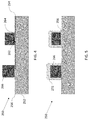
- FIG. 4 is a schematically illustrated cross sectional view of a wafer during a method of manufacturing wafer level interconnections in accordance with the subject technology.
- FIG. 5 is a schematically illustrated cross sectional view of a wafer during a method of manufacturing wafer level interconnections in accordance with the subject technology.
- FIG. 6 is a schematically illustrated cross sectional view of a wafer during a method of manufacturing wafer level interconnections in accordance with the subject technology.
- FIG. 7 is a schematically illustrated cross sectional view of a wafer during a method of manufacturing wafer level interconnections in accordance with the subject technology.
- FIG. 8 is a schematically illustrated cross sectional view of a wafer during a method of manufacturing wafer level interconnections in accordance with the subject technology.
- FIG. 9 is a schematically illustrated cross sectional view of a wafer during a method of manufacturing wafer level interconnections in accordance with the subject technology.
- FIG. 10 is a schematically illustrated cross sectional view of a bonded wafer assembly created by a method in accordance with the subject technology.
- the subject technology overcomes many of the prior art problems associated with the fabrication of semiconductor devices.
- the subject technology provides a method of manufacturing a wafer or wafer assembly, particularly one that can include Indium based interconnections.
- an “upper” surface of a part is merely meant to describe a surface that is separate from the “lower” surface of that same part, as shown in the figures.
- No words denoting orientation are used to describe an absolute orientation (i.e. where an “upper” part must always be on top).
- the method 100 generally involves creating interconnections on a wafer device such as a III-V semiconductor device and optionally bonding with a separate wafer to form a wafer assembly.
- the method 100 starts at first step 102 which includes providing a first wafer 250 with a device layer 252 , an insulating layer 254 , and a metal seed layer 256 , as seen in FIG. 2 .
- Preliminary steps of manufacturing the first wafer 250 are understood in the art and therefore a thorough description thereof is omitted.
- the device layer 252 is typically a Silicon substrate and includes processing circuitry extending therethrough comprised of Al, Cu, implantation or the like.
- the insulating layer 254 is positioned over the upper surface 260 of the device layer 252 and can be comprised of materials such as SiO 2 , SiN x , or the like.
- the metal seed layer 256 is provided for plating posts or interconnections, as is discussed more fully below, and is comprised of materials such as TiW, Al, Sn, or the like.
- the insulating layer 254 is broken by a first plurality of holes or perforations 262 through which the metal seed layer 256 extends, forming vias 264 .
- both the insulating layer 254 and the metal seed layer 256 may additionally or alternatively be comprised of other materials known in the art to function in accordance with the insulating layer 254 and metal seed layer 256 described herein.
- a photoresist (PR) pattern mold 268 is applied over the metal seed layer 256 .
- the PR pattern mold 268 is patterned with a second plurality of holes or perforations 270 which correspond to the perforations 262 in the insulating layer 254 .
- the Indium is plated within the PR pattern mold 268 to form an array of posts 266 .
- the PR pattern mold 268 allows for improved Indium plating uniformity and reduces Indium contamination from bonding oxide, as the Indium is not dragged across oxide.
- the posts 266 are formed as a small dense array that grows from the metal seed layer 256 when current is provided and will eventually serve as high yield fine pitch array for interconnections for the first wafer 250 .
- the posts 266 are grown within the perforations 270 which align with the vias 264 , such that the vias 264 connect the posts 266 to the device layer 252 .
- the posts 266 eventually form the interconnections on the first wafer 250 . While Indium has been found to be effectively used to form the posts 266 within the disclosed method 100 , it should be noted that the methods discussed herein are applicable to other elements and/or materials which can be used in the formation of wafer interconnections.
- the method 100 and other methods discussed herein have been found to be effective when the posts 266 which form the interconnections are comprised materials/elements with a low melting point, such as below 200 degrees Celsius. This is because the method 100 is designed to avoid melting material with a low melting point, whereas other process of forming interconnections and bonding wafers will often melt and/or deform such material.
- the PR pattern mold 268 is stripped as seen in FIG. 4 .
- a second PR layer 272 can optionally be placed surrounding the posts 266 at step 109 .
- the metal seed layer 256 is then etched to singulate the posts 266 such that the posts 266 are isolated from one another (i.e. not directly connected through the metal seed layer 256 ). Etching can be accomplished, for example, by photolithographic techniques as are known in the art.
- the second PR layer 272 protects the posts 266 during the metal etching process and can be stripped, at step 111 , after the etching process is complete.
- a low temperature oxide is applied over a surface 276 of the first wafer 250 (and around the posts 266 extending from the surface 276 ) as seen in FIG. 6 , to form an oxide layer 274 .
- the low temperature oxide is below the melting temperature of Indium, which is about 157 degrees Celsius. Therefore in at least some embodiments, the temperature of the low temperature oxide is applied at a temperature of below 150 degrees Celsius. In some embodiments, the low temperature oxide is applied at a temperature of substantially 20 degrees Celsius below the melting point of Indium, such as between 127 degrees Celsius and 147 degrees Celsius. In other embodiments, the temperature of the low temperature oxide is between 135 degrees Celsius and 139 degrees Celsius.
- corresponding oxide temperature ranges can be applied (e.g. substantially 20 degrees below a melting point of the other material).
- the oxide can be applied within one of the temperature ranges described above.
- a new surface 278 of the first wafer 250 is formed which is typically non-uniform. Therefore at step 114 , and as seen in FIG. 7 , chemical-mechanical polishing (CMP) is then applied to the non-uniform surface 278 . Applying CMP to the non-uniform surface 278 of the first wafer 250 removes excess post 266 and oxide layer 274 material to smooth and/or level the surface 278 . CMP is applied until the oxide layer 274 and posts 266 have been planarized, forming a flat and continuous upper surface 280 of the wafer 250 . A planarized surface 280 helps bond the first wafer 250 to a second wafer, as discussed below.
- CMP chemical-mechanical polishing
- FIG. 8 shows an optional intermediate step of placing a second PR layer 284 over the posts 266 to serve as a protective cap for the posts 266 during cleaning.
- Cleaning typically involves applying a substance, such as an acid, to the surface 282 of the oxide layer 274 .
- HCl can be applied over to the surface 282 of the oxide layer 274 .
- Cleaning the surface 282 removes contamination created by the formation of the posts 266 (e.g. Indium contamination on the oxide layer 274 ) and helps prepare the first wafer 250 for effective bonding with another wafer.
- the second PR layer 284 can be stripped from the posts 266 at FIG. 9 using any means known in the art. The first wafer 250 is now ready for bonding to another wafer.
- the first wafer 250 can be bonded to a second wafer 286 which is similar, or identical, to the first wafer 250 to form a wafer assembly 290 .
- the steps described above i.e. 102 - 116
- the second wafer 286 can likewise include posts 288 comprised of Indium (or other low temperature material for forming interconnections) at a similar position within the second wafer 286 as the posts 266 within the first wafer 250 .
- Forming posts 288 at a similar position within the second wafer 286 allows for good alignment of the posts 266 , 288 of the first and second wafers 250 , 286 .
- FIG. 10 shows the first wafer 250 and the second wafer 286 with similarly positioned posts 266 , 288 .
- the posts 266 of the first wafer 250 are then aligned with posts 288 of the second wafer 286 using a separate device (not shown in the figures).
- the wafers 250 , 286 are then bonded at step 122 to form the wafer assembly 290 .
- the bonding can be accomplished, for example, by a low temperature annealing process.
- the posts 266 , 288 provide interconnections between the wafers 250 , 286 .
- FIG. 1A a simplified method 130 of manufacturing a wafer in accordance with the subject technology is shown in FIG. 1B .
- the method 130 starts with plating an array of posts, such as posts 266 , on a substrate of first wafer 250 , such as is shown in FIG. 3 .
- the posts 266 can be grown off the metal seed layer 256 of a substrate comprised of a metal seed layer 256 , an insulating layer 254 , and a device layer 252 .
- the posts 266 can be grown within a PR pattern mold 268 .
- the post metal can be deposited using physical vapor deposition, Chemical vapor deposition, or the like.
- the PR pattern mold 268 can be stripped from the first wafer 250 as seen in FIG. 4 .
- a low temperature oxide is then applied over the surface of the first wafer 250 , a step 136 , to form an oxide layer 274 as seen in FIG. 6 .
- the low temperature oxide can be applied at a temperature of substantially 20 degrees Celsius below the melting point of the posts 266 .
- the posts 266 are Indium (which has a melting point of roughly 157 degrees Celsius)
- the low temperature can be applied between 127 degrees Celsius and 147 degrees Celsius, between 135 degrees Celsius and 139 degrees Celsius, or simply below 150 degrees Celsius.
- the low temperature oxide can be applied at a similar range below the melting temperature of other materials used to form the posts 266 , or alternatively, the aforementioned temperature ranges can be applied regardless of the material used.
- CMP is applied to the surface of the first wafer 250 to planarize a surface 280 formed by the posts 266 and oxide layer 274 , as seen in FIG. 7 .
- the first wafer 250 can then be optionally cleaned, as discussed with respect to step 116 , and then bonded to a second wafer 286 to form a wafer assembly 290 , as discussed in steps 120 - 122 and as shown in FIG. 10 .
- any of the steps or combinations of steps disclosed in FIG. 1A with respect to method 100 and/or shown in the figures herein can be combined with the steps disclosed in FIG. 1B with respect to method 130 to provide additional benefits if desired.
- any functional element may perform fewer, or different, operations than those described with respect to the illustrated embodiment.
- functional elements e.g. molds and the like
- shown as distinct for purposes of illustration may be incorporated within other functional elements in a particular implementation.
Landscapes
- Chemical & Material Sciences (AREA)
- Engineering & Computer Science (AREA)
- Metallurgy (AREA)
- Chemical Kinetics & Catalysis (AREA)
- Materials Engineering (AREA)
- Organic Chemistry (AREA)
- Mechanical Engineering (AREA)
- General Chemical & Material Sciences (AREA)
- Microelectronics & Electronic Packaging (AREA)
- Manufacturing & Machinery (AREA)
- Electrochemistry (AREA)
- Internal Circuitry In Semiconductor Integrated Circuit Devices (AREA)
- Mechanical Treatment Of Semiconductor (AREA)
- Electrodes Of Semiconductors (AREA)
Abstract
Description
Claims (17)
Priority Applications (11)
| Application Number | Priority Date | Filing Date | Title |
|---|---|---|---|
| US15/895,512 US10504777B2 (en) | 2018-02-13 | 2018-02-13 | Method of manufacturing wafer level low melting temperature interconnections |
| PCT/US2018/047250 WO2019160577A1 (en) | 2018-02-13 | 2018-08-21 | Method of manufacturing wafer level low melting temperature interconnections for a wafer bonding assembly |
| KR1020207018560A KR20200094184A (en) | 2018-02-13 | 2018-08-21 | Method for manufacturing wafer level low melting temperature wiring for wafer bonding assembly |
| SG11202005738YA SG11202005738YA (en) | 2018-02-13 | 2018-08-21 | Method of manufacturing wafer level low melting temperature interconnections for a wafer bonding assembly |
| CA3090868A CA3090868C (en) | 2018-02-13 | 2018-08-21 | Method of manufacturing wafer level low melting temperature interconnections for a wafer bonding assembly |
| EP18773680.6A EP3753045B1 (en) | 2018-02-13 | 2018-08-21 | Method of manufacturing wafer level low melting temperature interconnections for a wafer bonding assembly |
| JP2020532558A JP7076551B2 (en) | 2018-02-13 | 2018-08-21 | Wafer Level Low Melting Point Interconnect Manufacturing Method |
| CN201880087992.2A CN111656495A (en) | 2018-02-13 | 2018-08-21 | Method of fabricating wafer-level low melting temperature interconnects for wafer-bonded assemblies |
| TW107135037A TWI711093B (en) | 2018-02-13 | 2018-10-04 | Method of manufacturing wafer level low melting temperature interconnections |
| US16/675,992 US11222813B2 (en) | 2018-02-13 | 2019-11-06 | Method of manufacturing wafer level low melting temperature interconnections |
| IL275119A IL275119A (en) | 2018-02-13 | 2020-06-04 | Method of manufacturing wafer level low melting temperature interconnections for a wafer bonding assembly |
Applications Claiming Priority (1)
| Application Number | Priority Date | Filing Date | Title |
|---|---|---|---|
| US15/895,512 US10504777B2 (en) | 2018-02-13 | 2018-02-13 | Method of manufacturing wafer level low melting temperature interconnections |
Related Child Applications (1)
| Application Number | Title | Priority Date | Filing Date |
|---|---|---|---|
| US16/675,992 Continuation US11222813B2 (en) | 2018-02-13 | 2019-11-06 | Method of manufacturing wafer level low melting temperature interconnections |
Publications (2)
| Publication Number | Publication Date |
|---|---|
| US20190252244A1 US20190252244A1 (en) | 2019-08-15 |
| US10504777B2 true US10504777B2 (en) | 2019-12-10 |
Family
ID=63668004
Family Applications (2)
| Application Number | Title | Priority Date | Filing Date |
|---|---|---|---|
| US15/895,512 Active US10504777B2 (en) | 2018-02-13 | 2018-02-13 | Method of manufacturing wafer level low melting temperature interconnections |
| US16/675,992 Active US11222813B2 (en) | 2018-02-13 | 2019-11-06 | Method of manufacturing wafer level low melting temperature interconnections |
Family Applications After (1)
| Application Number | Title | Priority Date | Filing Date |
|---|---|---|---|
| US16/675,992 Active US11222813B2 (en) | 2018-02-13 | 2019-11-06 | Method of manufacturing wafer level low melting temperature interconnections |
Country Status (10)
| Country | Link |
|---|---|
| US (2) | US10504777B2 (en) |
| EP (1) | EP3753045B1 (en) |
| JP (1) | JP7076551B2 (en) |
| KR (1) | KR20200094184A (en) |
| CN (1) | CN111656495A (en) |
| CA (1) | CA3090868C (en) |
| IL (1) | IL275119A (en) |
| SG (1) | SG11202005738YA (en) |
| TW (1) | TWI711093B (en) |
| WO (1) | WO2019160577A1 (en) |
Families Citing this family (4)
| Publication number | Priority date | Publication date | Assignee | Title |
|---|---|---|---|---|
| US11430753B2 (en) | 2020-07-08 | 2022-08-30 | Raytheon Company | Iterative formation of damascene interconnects |
| CN114178979A (en) * | 2021-12-16 | 2022-03-15 | 华虹半导体(无锡)有限公司 | Method for optimizing CMP cleaning capacity |
| CN116261392B (en) * | 2023-01-17 | 2024-09-20 | 深圳量旋科技有限公司 | Superconducting quantum chip and substrate thereof, and manufacturing method of substrate |
| CN115955906B (en) * | 2023-01-20 | 2025-05-30 | 深圳量旋科技有限公司 | Superconducting quantum chip, substrate thereof, and method for manufacturing the substrate |
Citations (8)
| Publication number | Priority date | Publication date | Assignee | Title |
|---|---|---|---|---|
| US20020004288A1 (en) | 2000-04-28 | 2002-01-10 | Kazuo Nishiyama | Chip-like electronic components, a method of manufacturing the same, a pseudo wafer therefor and a method of manufacturing thereof |
| US20060292851A1 (en) | 2005-06-24 | 2006-12-28 | Mou-Shiung Lin | Circuitry component and method for forming the same |
| US20120313237A1 (en) | 2010-02-04 | 2012-12-13 | Soitec | Bonded semiconductor structures and methods of forming same |
| US20160079034A1 (en) * | 2014-09-12 | 2016-03-17 | Applied Materials Inc. | Flowable film properties tuning using implantation |
| US20170271217A1 (en) | 2016-03-15 | 2017-09-21 | Raytheon Company | In-situ calibration structures and methods of use in semiconductor processing |
| US20170287696A1 (en) * | 2014-09-19 | 2017-10-05 | Hitachi Kokusai Electric Inc. | Method of manufacturing semiconductor device, substrate processing apparatus, and recording medium |
| US20180040546A1 (en) * | 2016-08-05 | 2018-02-08 | Taiwan Semiconductor Manufacturing Company, Ltd. | Dense redistribution layers in semiconductor packages and methods of forming the same |
| US20180151389A1 (en) * | 2016-11-29 | 2018-05-31 | Taiwan Semiconductor Manufacturing Co., Ltd. | Inter-fan-out wafer level packaging with coaxial tiv for 3d ic low-noise packaging |
Family Cites Families (13)
| Publication number | Priority date | Publication date | Assignee | Title |
|---|---|---|---|---|
| JP2006093357A (en) * | 2004-09-22 | 2006-04-06 | Ebara Corp | Semiconductor device, manufacturing method thereof, and processing liquid |
| JP4998073B2 (en) * | 2007-05-07 | 2012-08-15 | ソニー株式会社 | Semiconductor chip and manufacturing method thereof |
| US9524945B2 (en) * | 2010-05-18 | 2016-12-20 | Taiwan Semiconductor Manufacturing Company, Ltd. | Cu pillar bump with L-shaped non-metal sidewall protection structure |
| US7863097B2 (en) * | 2008-11-07 | 2011-01-04 | Raytheon Company | Method of preparing detectors for oxide bonding to readout integrated chips |
| JP2013207067A (en) * | 2012-03-28 | 2013-10-07 | Jsr Corp | Semiconductor device and manufacturing method of the same |
| US9318640B2 (en) * | 2013-03-15 | 2016-04-19 | Taiwan Semiconductor Manufacturing Company, Ltd. | Method and apparatus for image sensor packaging |
| JP2014241320A (en) * | 2013-06-11 | 2014-12-25 | ソニー株式会社 | Semiconductor device and method for manufacturing the same |
| CN105448750A (en) * | 2014-08-28 | 2016-03-30 | 中芯国际集成电路制造(上海)有限公司 | Semiconductor device and manufacturing method thereof, and electronic device |
| CN105633008B (en) * | 2014-11-06 | 2019-04-23 | 中国科学院苏州纳米技术与纳米仿生研究所 | A kind of preparation method of indium column, infrared focal plane array detector |
| KR102586317B1 (en) * | 2014-12-22 | 2023-10-06 | 바스프 에스이 | Use of a chemical mechanical polishing (cmp) composition for polishing of cobalt and/or cobalt alloy comprising substrates |
| TW201737428A (en) * | 2016-03-22 | 2017-10-16 | 台灣積體電路製造股份有限公司 | Semiconductor package |
| US10354975B2 (en) * | 2016-05-16 | 2019-07-16 | Raytheon Company | Barrier layer for interconnects in 3D integrated device |
| US9748206B1 (en) * | 2016-05-26 | 2017-08-29 | Taiwan Semiconductor Manufacturing Co., Ltd. | Three-dimensional stacking structure and manufacturing method thereof |
-
2018
- 2018-02-13 US US15/895,512 patent/US10504777B2/en active Active
- 2018-08-21 CN CN201880087992.2A patent/CN111656495A/en active Pending
- 2018-08-21 EP EP18773680.6A patent/EP3753045B1/en active Active
- 2018-08-21 WO PCT/US2018/047250 patent/WO2019160577A1/en not_active Ceased
- 2018-08-21 CA CA3090868A patent/CA3090868C/en active Active
- 2018-08-21 SG SG11202005738YA patent/SG11202005738YA/en unknown
- 2018-08-21 JP JP2020532558A patent/JP7076551B2/en not_active Expired - Fee Related
- 2018-08-21 KR KR1020207018560A patent/KR20200094184A/en not_active Abandoned
- 2018-10-04 TW TW107135037A patent/TWI711093B/en not_active IP Right Cessation
-
2019
- 2019-11-06 US US16/675,992 patent/US11222813B2/en active Active
-
2020
- 2020-06-04 IL IL275119A patent/IL275119A/en active IP Right Grant
Patent Citations (8)
| Publication number | Priority date | Publication date | Assignee | Title |
|---|---|---|---|---|
| US20020004288A1 (en) | 2000-04-28 | 2002-01-10 | Kazuo Nishiyama | Chip-like electronic components, a method of manufacturing the same, a pseudo wafer therefor and a method of manufacturing thereof |
| US20060292851A1 (en) | 2005-06-24 | 2006-12-28 | Mou-Shiung Lin | Circuitry component and method for forming the same |
| US20120313237A1 (en) | 2010-02-04 | 2012-12-13 | Soitec | Bonded semiconductor structures and methods of forming same |
| US20160079034A1 (en) * | 2014-09-12 | 2016-03-17 | Applied Materials Inc. | Flowable film properties tuning using implantation |
| US20170287696A1 (en) * | 2014-09-19 | 2017-10-05 | Hitachi Kokusai Electric Inc. | Method of manufacturing semiconductor device, substrate processing apparatus, and recording medium |
| US20170271217A1 (en) | 2016-03-15 | 2017-09-21 | Raytheon Company | In-situ calibration structures and methods of use in semiconductor processing |
| US20180040546A1 (en) * | 2016-08-05 | 2018-02-08 | Taiwan Semiconductor Manufacturing Company, Ltd. | Dense redistribution layers in semiconductor packages and methods of forming the same |
| US20180151389A1 (en) * | 2016-11-29 | 2018-05-31 | Taiwan Semiconductor Manufacturing Co., Ltd. | Inter-fan-out wafer level packaging with coaxial tiv for 3d ic low-noise packaging |
Non-Patent Citations (2)
| Title |
|---|
| Chen et al., "Wafer-scale 3D integration of InGaAs photodiode arrays with Si readout circuits by oxide bonding and through-oxide vias," Microelectronic Engineering, Elsevier Publishers BV., Amsterdam, NL, vol. 88, No. 1, Jan. 1, 2011, pp. 131-134. |
| International Search Report and Written Opinion from related PCT Application No. PCT/US2018/047250 dated Dec. 14, 2018. |
Also Published As
| Publication number | Publication date |
|---|---|
| IL275119A (en) | 2020-07-30 |
| US20200075396A1 (en) | 2020-03-05 |
| CA3090868C (en) | 2021-10-12 |
| JP2021506137A (en) | 2021-02-18 |
| EP3753045B1 (en) | 2025-04-09 |
| CA3090868A1 (en) | 2019-08-22 |
| WO2019160577A1 (en) | 2019-08-22 |
| TW201941322A (en) | 2019-10-16 |
| US20190252244A1 (en) | 2019-08-15 |
| JP7076551B2 (en) | 2022-05-27 |
| EP3753045A1 (en) | 2020-12-23 |
| CN111656495A (en) | 2020-09-11 |
| TWI711093B (en) | 2020-11-21 |
| KR20200094184A (en) | 2020-08-06 |
| SG11202005738YA (en) | 2020-07-29 |
| US11222813B2 (en) | 2022-01-11 |
Similar Documents
| Publication | Publication Date | Title |
|---|---|---|
| US11222813B2 (en) | Method of manufacturing wafer level low melting temperature interconnections | |
| US11894326B2 (en) | Multi-metal contact structure | |
| US6908565B2 (en) | Etch thinning techniques for wafer-to-wafer vertical stacks | |
| TW202545028A (en) | Via reveal processing and structures | |
| US8853005B2 (en) | Method for manufacturing semiconductor device | |
| US6674168B1 (en) | Single and multilevel rework | |
| CN102165587A (en) | Method for fabricating through interconnection on semiconductor substrate | |
| US12300759B2 (en) | Method of manufacturing a hybrid device | |
| US20240170475A1 (en) | Method for manufacturing semiconductor device, semiconductor device, integrated circuit element, and method for manufacturing integrated circuit element | |
| US8329573B2 (en) | Wafer level integration module having controlled resistivity interconnects | |
| US20040130034A1 (en) | Method for forming a wafer level chip scale package | |
| US6242337B1 (en) | Semiconductor device and method of manufacturing the same | |
| CN101663742B (en) | Front-end processing wafer with through-chip connections | |
| US20100330796A1 (en) | Manufacturing method of semiconductor device | |
| US9449867B2 (en) | VHF etch barrier for semiconductor integrated microsystem | |
| US9899297B1 (en) | Semiconductor device having a through-silicon via and manufacturing method thereof | |
| US20200395248A1 (en) | Forming ultra-thin chips for flexible electronics applications | |
| US7307010B2 (en) | Method for processing a thin semiconductor substrate | |
| US9812404B2 (en) | Electrical connection around a crackstop structure | |
| US6074948A (en) | Method for manufacturing thin semiconductor device | |
| KR102200437B1 (en) | Method for manufacturing through hole electrode | |
| CN110660727A (en) | Method for forming semiconductor device structure | |
| JPH036024A (en) | Manufacture of semiconductor device |
Legal Events
| Date | Code | Title | Description |
|---|---|---|---|
| FEPP | Fee payment procedure |
Free format text: ENTITY STATUS SET TO UNDISCOUNTED (ORIGINAL EVENT CODE: BIG.); ENTITY STATUS OF PATENT OWNER: LARGE ENTITY |
|
| AS | Assignment |
Owner name: RAYTHEON COMPANY, MASSACHUSETTS Free format text: ASSIGNMENT OF ASSIGNORS INTEREST;ASSIGNORS:KILCOYNE, SEAN P.;GRAMA, GEORGE;MILLER, ERIC R.;REEL/FRAME:045421/0968 Effective date: 20180212 |
|
| STPP | Information on status: patent application and granting procedure in general |
Free format text: DOCKETED NEW CASE - READY FOR EXAMINATION |
|
| STPP | Information on status: patent application and granting procedure in general |
Free format text: NOTICE OF ALLOWANCE MAILED -- APPLICATION RECEIVED IN OFFICE OF PUBLICATIONS |
|
| STCF | Information on status: patent grant |
Free format text: PATENTED CASE |
|
| MAFP | Maintenance fee payment |
Free format text: PAYMENT OF MAINTENANCE FEE, 4TH YEAR, LARGE ENTITY (ORIGINAL EVENT CODE: M1551); ENTITY STATUS OF PATENT OWNER: LARGE ENTITY Year of fee payment: 4 |