US10341556B2 - Image capturing apparatus and control method therefor - Google Patents
Image capturing apparatus and control method therefor Download PDFInfo
- Publication number
- US10341556B2 US10341556B2 US15/727,928 US201715727928A US10341556B2 US 10341556 B2 US10341556 B2 US 10341556B2 US 201715727928 A US201715727928 A US 201715727928A US 10341556 B2 US10341556 B2 US 10341556B2
- Authority
- US
- United States
- Prior art keywords
- read
- rows
- signals
- control
- out control
- Prior art date
- Legal status (The legal status is an assumption and is not a legal conclusion. Google has not performed a legal analysis and makes no representation as to the accuracy of the status listed.)
- Active, expires
Links
- 238000000034 method Methods 0.000 title claims description 38
- 238000001514 detection method Methods 0.000 claims abstract description 62
- 238000006243 chemical reaction Methods 0.000 claims abstract description 50
- 239000011159 matrix material Substances 0.000 claims abstract description 8
- 230000003321 amplification Effects 0.000 claims abstract description 3
- 238000003199 nucleic acid amplification method Methods 0.000 claims abstract description 3
- 230000001629 suppression Effects 0.000 claims description 18
- 230000009467 reduction Effects 0.000 claims description 14
- 230000007423 decrease Effects 0.000 claims description 3
- 230000008569 process Effects 0.000 description 19
- 238000010586 diagram Methods 0.000 description 9
- 230000003287 optical effect Effects 0.000 description 8
- 230000006870 function Effects 0.000 description 6
- 210000001747 pupil Anatomy 0.000 description 6
- 238000011156 evaluation Methods 0.000 description 5
- 230000004907 flux Effects 0.000 description 3
- 238000003384 imaging method Methods 0.000 description 2
- 230000008901 benefit Effects 0.000 description 1
- 230000008859 change Effects 0.000 description 1
- 239000003086 colorant Substances 0.000 description 1
- 230000003247 decreasing effect Effects 0.000 description 1
- 238000012986 modification Methods 0.000 description 1
- 230000004048 modification Effects 0.000 description 1
- 230000002093 peripheral effect Effects 0.000 description 1
- 230000004044 response Effects 0.000 description 1
- 238000004904 shortening Methods 0.000 description 1
- 230000002194 synthesizing effect Effects 0.000 description 1
Images


Classifications
-
- H04N5/23229—
-
- H01L27/14627—
-
- H—ELECTRICITY
- H04—ELECTRIC COMMUNICATION TECHNIQUE
- H04N—PICTORIAL COMMUNICATION, e.g. TELEVISION
- H04N23/00—Cameras or camera modules comprising electronic image sensors; Control thereof
- H04N23/45—Cameras or camera modules comprising electronic image sensors; Control thereof for generating image signals from two or more image sensors being of different type or operating in different modes, e.g. with a CMOS sensor for moving images in combination with a charge-coupled device [CCD] for still images
-
- H—ELECTRICITY
- H04—ELECTRIC COMMUNICATION TECHNIQUE
- H04N—PICTORIAL COMMUNICATION, e.g. TELEVISION
- H04N23/00—Cameras or camera modules comprising electronic image sensors; Control thereof
- H04N23/60—Control of cameras or camera modules
- H04N23/67—Focus control based on electronic image sensor signals
- H04N23/672—Focus control based on electronic image sensor signals based on the phase difference signals
-
- H—ELECTRICITY
- H04—ELECTRIC COMMUNICATION TECHNIQUE
- H04N—PICTORIAL COMMUNICATION, e.g. TELEVISION
- H04N23/00—Cameras or camera modules comprising electronic image sensors; Control thereof
- H04N23/80—Camera processing pipelines; Components thereof
-
- H—ELECTRICITY
- H04—ELECTRIC COMMUNICATION TECHNIQUE
- H04N—PICTORIAL COMMUNICATION, e.g. TELEVISION
- H04N25/00—Circuitry of solid-state image sensors [SSIS]; Control thereof
- H04N25/10—Circuitry of solid-state image sensors [SSIS]; Control thereof for transforming different wavelengths into image signals
- H04N25/11—Arrangement of colour filter arrays [CFA]; Filter mosaics
- H04N25/13—Arrangement of colour filter arrays [CFA]; Filter mosaics characterised by the spectral characteristics of the filter elements
- H04N25/134—Arrangement of colour filter arrays [CFA]; Filter mosaics characterised by the spectral characteristics of the filter elements based on three different wavelength filter elements
-
- H—ELECTRICITY
- H04—ELECTRIC COMMUNICATION TECHNIQUE
- H04N—PICTORIAL COMMUNICATION, e.g. TELEVISION
- H04N25/00—Circuitry of solid-state image sensors [SSIS]; Control thereof
- H04N25/70—SSIS architectures; Circuits associated therewith
- H04N25/703—SSIS architectures incorporating pixels for producing signals other than image signals
- H04N25/704—Pixels specially adapted for focusing, e.g. phase difference pixel sets
-
- H04N5/2258—
-
- H04N5/232122—
-
- H04N5/3696—
-
- H—ELECTRICITY
- H04—ELECTRIC COMMUNICATION TECHNIQUE
- H04N—PICTORIAL COMMUNICATION, e.g. TELEVISION
- H04N5/00—Details of television systems
- H04N5/72—Modifying the appearance of television pictures by optical filters or diffusing screens
-
- H04N9/045—
-
- H—ELECTRICITY
- H10—SEMICONDUCTOR DEVICES; ELECTRIC SOLID-STATE DEVICES NOT OTHERWISE PROVIDED FOR
- H10F—INORGANIC SEMICONDUCTOR DEVICES SENSITIVE TO INFRARED RADIATION, LIGHT, ELECTROMAGNETIC RADIATION OF SHORTER WAVELENGTH OR CORPUSCULAR RADIATION
- H10F39/00—Integrated devices, or assemblies of multiple devices, comprising at least one element covered by group H10F30/00, e.g. radiation detectors comprising photodiode arrays
- H10F39/80—Constructional details of image sensors
- H10F39/806—Optical elements or arrangements associated with the image sensors
- H10F39/8063—Microlenses
Definitions
- the present invention relates to an image capturing apparatus and a control method therefor, and more particularly to an image capturing apparatus capable of reading a pair of signals from each pixel based on light beams passing through different pupil regions of an optical system and a control method thereof.
- Japanese Patent Laid-Open No. 2007-325139 which discloses an image sensor having pixels for information acquisition for focus detection that can also serve as pixels for image acquisition for acquiring an image signal
- each pixel for the information acquisition is divided into four regions in the horizontal direction and the vertical direction and it is possible to obtain an image signal by adding all the signals of the four divided regions at the time of image acquisition.
- the pupil division of each pixel is realized and the obtained signals can be used as focus adjustment signals for on-imaging plane phase difference focus control.
- Japanese Patent Laid-Open No. 2012-155095 suggests an image capturing apparatus capable of shortening the time required to read out the image signal from the image sensor while setting the information acquisition region for focus detection in an arbitrary area in the image sensor.
- signals are independently read from a plurality of photoelectric conversion portions of each pixel subjected to pupil division, and the independently read out signals are added in the image capturing apparatus to generate an image signal.
- the signals of the plurality of photoelectric conversion portions are added for each pixel in the image sensor, then are read out to obtain the image signal.
- the level of the noise differs between an image signal obtained from the information acquisition region and an image signal obtained from the image acquisition region, and there is a problem that a noise difference between the regions appears in the image.
- the present invention has been made in consideration of the above situation, and makes the difference in noise between the information acquisition area for focus detection and the image acquisition area for image signal acquisition inconspicuous when the on-imaging plane phase difference focus control is performed.
- an image capturing apparatus comprising: an image sensor having a plurality of photoelectric conversion portions that correspond to each of a plurality of microlenses arranged in a matrix; a control circuit that controls read-out from the image sensor by either of a first read-out control and second read-out control, wherein the first read-out control is to read out signals from the plurality of photoelectric conversion portions so as to be able to obtain pupil-divided signals, and the second read-out control is to combine signals of the plurality of photoelectric conversion portions corresponding to each microlens and read out an image signal; a setting circuit that sets rows to be read out by the first read-out control among rows that include a focus detection area for which focus detection is performed; an amplification circuit that amplifies a signal read out from the image sensor with a gain set in accordance with an exposure state; and a signal processing circuit that performs signal processing on an image signal corresponding to each microlens obtained from the signals read out by the first read-out control and on
- a control method for an image capturing apparatus including an image sensor having a plurality of photoelectric conversion portions that correspond to each of a plurality of microlenses arranged in a matrix, the method comprising: setting rows to be read out by a first read-out control for reading out signals from the plurality of photoelectric conversion portions so as to be able to obtain pupil-divided signals among rows that include a focus detection area for which focus detection is performed; reading out signals from the plurality of photoelectric conversion portions of the image sensor by either of first read-out control and second read-out control for combining signals of the plurality of photoelectric conversion portions corresponding to each microlens and reading out an image signal; amplifying a signal read out from the image sensor with a gain set in accordance with an exposure state; and performing signal processing on an image signal corresponding to each microlens obtained from the signals read out by the first read-out control and on the image signal corresponding to each microlens read out by the second read-out control using an image signal
- a non-transitory storage medium readable by a computer, the storage medium storing a program that is executable by the computer, wherein the program includes program code for causing the computer to perform a control method for an image capturing apparatus including an image sensor having a plurality of photoelectric conversion portions that correspond to each of a plurality of microlenses arranged in a matrix, comprising: setting rows to be read out by a first read-out control for reading out signals from the plurality of photoelectric conversion portions so as to be able to obtain pupil-divided signals among rows that include a focus detection area for which focus detection is performed; reading out signals from the plurality of photoelectric conversion portions of the image sensor by either of first read-out control and second read-out control for combining signals of the plurality of photoelectric conversion portions corresponding to each microlens and reading out an image signal; amplifying a signal read out from the image sensor with a gain set in accordance with an exposure state; and performing signal processing on an image signal corresponding to
- FIG. 1 is a block diagram showing a schematic configuration of an image capturing apparatus according to a first embodiment of the present invention
- FIG. 2A and FIG. 2B are diagrams showing a configuration example of an image sensor according to an embodiment
- FIGS. 3A to 3C are diagrams for explaining a relationship between an information acquisition region, an image acquisition region, and filter processing according to the first embodiment
- FIG. 4 is a flowchart showing a control operation by a read-out region control circuit in the first embodiment
- FIG. 5 is a block diagram showing a schematic configuration of an image capturing apparatus according to a second embodiment.
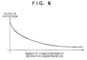
- FIG. 6 is a diagram showing a suppression degree of a noise reduction circuit according to the second embodiment.
- FIG. 1 is a block diagram showing a schematic configuration of an image capturing apparatus according to a first embodiment of the present invention.
- an optical system 1 including a zoom lens, a focus lens, and a diaphragm drives the diaphragm and lenses in response to a control signal from an optical system driving circuit 2 to form a subject image controlled to an appropriate brightness onto an image sensor 3 .
- the image sensor 3 has a plurality of photoelectric conversion portions for respectively receiving light fluxes having passed through different regions of an exit pupil of the optical system 1 , converting them into electric signals by photoelectric conversion, and outputting pupil-divided image signals.
- the image sensor 3 is driven by a drive pulse controlled by the image sensor driving circuit 4 , and signals are read out so that a pair of pupil-divided focus detection signals can be individually acquired.
- pupil-divided electric signals are independently read out from the plurality of photoelectric conversion portions 211 a and 211 b .
- pupil-divided electric signals of the plurality of photoelectric conversion portions 211 a and 211 b are combined for each pixel in the image sensor 3 and read out.
- the drive pulse from the image sensor driving circuit 4 is controlled based on parallax image acquisition region information from the read-out region control circuit 11 .
- FIG. 2A shows a pixel array of the image sensor 3 in the present embodiment.
- the range of 6 rows in the longitudinal direction (Y direction) and 8 rows in the lateral direction (X direction) of the two-dimensional CMOS area sensor is observed from the side of the optical system 1 .
- the image sensor 3 is provided with a Bayer array color filter.
- color filters of green (G) and red (R) are alternately arranged in the X direction in order from the left in the pixels of odd-numbered rows
- color filters of blue (B) and green (G) color filters are alternately arranged in the X direction in order from the left in the pixels of even-numbered rows.
- a plurality of rectangles arranged inside of each on-chip microlens 211 i arranged in a matrix form represent photoelectric conversion portions 211 a and 211 b , respectively.
- the photoelectric conversion portions 211 a and 211 b included in the image sensor 3 of the present embodiment receive light fluxes passing through different partial pupil regions of the optical system 1 and convert them into electric signals.
- the photoelectric conversion portions of every pixel of the image sensor 3 are divided into two regions in the X direction, and signals can be independently read from the plurality of photoelectric conversion portions 211 a and 211 b , however, the present invention is not limited to this.
- a pixel may be divided in the Y direction, or divided into a plurality of portions in the X direction and the Y direction. Then, by adding the readout signals for each pixel, it is possible to obtain an image signal for each pixel.
- an image signal is acquired by adding the signal of the photoelectric conversion portion 211 a and the signal of the photoelectric conversion portion 211 b .
- the photoelectric conversion signals of these divided photoelectric conversion portions can be used not only for known phase difference focus detection but also for generating a stereoscopic (3D) image composed of a plurality of images having parallax information.
- the sum of the two photoelectric conversion signals is used as a normal shot image.
- the signal is read out from each of the plurality of photoelectric conversion portions of each pixel of the image sensor 3 , but the present invention is not limited to this.
- it may be configured so that, by reading out a focus detection signal of one of the photoelectric conversion portions 211 a and 211 b and a signal obtained by combining signals of the photoelectric conversion portions 211 a and 211 b for each pixel, and subtracting the focus detection signal from the combined image signal, the other focus detection signal is obtained.
- FIG. 2B is a diagram showing a configuration example of a read out circuit of the image sensor 3 according to the embodiment.
- Reference numeral 151 denotes a horizontal scanning circuit
- reference numeral 153 denotes a vertical scanning circuit.
- Horizontal scan lines 152 a and 152 b and vertical scan lines 154 a and 154 b are arranged at the boundary of each pixel and signals are read out from each of the photoelectric conversion portions 211 a and 211 b to the outside through these scan lines.
- An exposure evaluation value calculation circuit 5 detects an exposure state based on the image signal obtained from the image sensor 3 having the above configuration and controls the aperture so that an appropriate exposure is attained for the entire image. If the brightness is insufficient even when the aperture is fully-opened, a gain is generated so that the image signal has an appropriate brightness and output to an exposure control circuit 6 .
- the exposure control circuit 6 applies the gain received from the exposure evaluation value calculation circuit 5 to the signal output from the image sensor 3 to amplify it, and outputs the amplified signal to a focus detection circuit 7 and a developing circuit 8 .
- the focus detection circuit 7 performs phase difference AF using a pair of pupil-divided focus detection signals output from the exposure control circuit 6 to obtain a focus state.
- the light flux that exits from the photographing optical system is pupil divided by the micro lens 211 i and the divided photoelectric conversion portions 211 a and 211 b shown in FIG. 2A . Then, for a plurality of pixels 211 in a predetermined region arranged in the same pixel row, the outputs of the photoelectric conversion portions 211 a are combined to form a first focus detection signal (AF image A). Similarly, the outputs of the photoelectric conversion portions 211 b are combined to form a second focus detection signal (AF image B).
- AF image A first focus detection signal
- AF image B second focus detection signal
- the outputs of the photoelectric conversion portions 211 a and 211 b are outputs of color components of one of a plurality of colors of green, red, blue, and green included in the unit array of the color filter, a pseudo luminance (Y) signal generated by synthesizing these outputs is used.
- the AF image A and the AF image B may be generated for each color of red, blue, and green.
- the amount of defocus (defocus amount) in a predetermined region can be detected by detecting a relative image shift amount between the AF image A and the AF image B generated in this manner by correlation calculation. Since such an image sensor is well known as disclosed in Japanese Patent Laid-Open No. 2004-134867, a description of further details will be omitted.
- the developing circuit 8 includes an LPF 81 with three taps of the same color and generates an image signal of each pixel from the focus detection signal read from the information acquisition region out of the signals output from the exposure control circuit 6 . Then, the developing circuit 8 performs low-pass filter (LPF) processing on the generated image signal together with the image signal read out from the image acquisition region. Further, the developing circuit 8 converts the LPF processed image signal into a luminance/color difference signal.
- LPF low-pass filter
- the pupil-divided focus detection signals are independently read out from the photoelectric conversion portions 211 a and 211 b , and the readout focus detection signals are added in the image capturing apparatus to generate image signals.
- the image acquisition region pupil-divided electric signals from a plurality of photoelectric conversion portions corresponding to each microlens 211 i are combined in the image sensor 3 and then read out. The larger the gain from the exposure evaluation value calculation circuit 5 is, the more the noise difference in each unit region in these two regions is emphasized.
- the image capturing apparatus usually has a process that refers to peripheral pixels for a pixel of interest like filter processing.
- a process that refers to peripheral pixels for a pixel of interest like filter processing.
- the noise difference becomes small.
- the information acquisition regions are discretely set so that signals of pixels with large noise difference are mixed by calculation to reduce the noise difference. Further, when the gain level is low and the noise difference is difficult to see, the information acquisition region is set continuously, and the focus adjustment of the ordinary phase difference method is performed. This makes it possible to perform the focus adjustment of the phase difference method while making it difficult to see the noise difference between the information acquisition region and the image acquisition region.
- FIGS. 3A to 3C are diagrams showing a part of pixels including the focus detection area indicated by a focus detection frame 300 , among the pixels forming the image sensor 3 .
- an area not hatched indicates the image acquisition region, and a hatched area indicates the information acquisition regions.
- the focus detection circuit 7 performs focus detection using the image signal read out from the information acquisition region within the focus detection frame 300 .
- the rows (n+6), (n+8), and (n+10) indicate a reference range of the LPF 81 when a pixel in the row (n+8) is taken as the pixel of interest in the LPF 81 with three taps of the same color in the developing circuit 8 .
- the noise here is assumed to be an offset component generated in the reading process of the image sensor 3 .
- FIG. 3A shows the relationship between the image acquisition region, the information acquisition region, and the rows (n+6), (n+8), and (n+10) when the gain level is low.
- FIG. 3B shows the relationship between the image acquisition region, the information acquisition region, and the rows (n+6), (n+8), and (n+10) when the gain level is medium.
- FIG. 3C shows the relationship between the image acquisition region, the information acquisition region, the rows (n+6), (n+8), and (n+10) when the gain level is high.
- the information acquisition region is continuously set.
- LPF processing with LPF 81 with three taps of the same color.
- the LPF 81 performs calculation by referring to the pixels of the rows (n+8), (n+10) with the pixel of the row (n+6) as the pixel of interest. Since the rows (n+6), (n+8) and (n+10) are both included in the information acquisition region, the offset component after the LPF process is the same as before the LPF process.
- the offset components are mixed and becomes close to the offset component when LPF processing is performed only on the pixels in the image acquisition region.
- the more pixels in the image acquisition region are mixed with the reference pixels in the LPF process the closer it is to the offset component when the LPF process is performed on only the pixels in the image acquisition region, and the noise difference between the information acquisition region and the image acquisition region becomes difficult to see.
- the luminance/color difference signals LPF processed by the developing circuit 8 as described above are output to a memory 9 and a main subject detection circuit 10 .
- the memory 9 records the luminance/color difference signals from the developing circuit 8 on a recording medium (not shown) or the like.
- the main subject detection circuit 10 detects the position of the main subject from the image signal developed by the developing circuit 8 and outputs subject information indicating the position and size thereof to a system control circuit 12 .
- the read-out region control circuit 11 determines the information acquisition region and the image acquisition region based on the position and size of the main subject detected by the main subject detection circuit 10 and the gain from the exposure evaluation value calculation circuit 5 , outputs the determined regions to image sensor driving circuit 4 .
- the system control circuit 12 controls entire of the image capturing apparatus.
- the control operation of the read-out region control circuit 11 according to the first embodiment will be described with reference to the flowchart in FIG. 4 .
- the gain generated by the exposure evaluation value calculation circuit 5 is acquired, and the process proceeds to S 102 .
- the generated gain level is compared with a threshold Thg 1 and a threshold Thg 2 (Thg 1 >Thg 2 ).
- the gain level is larger than the threshold value Thg 1 , it is judged that the gain level is high, if the gain level is less than or equal to the threshold value Thg 1 and is greater than the threshold value Thg 2 , it is judged that the gain level is medium, and if the gain level is less than the threshold value Thg 2 , it is judged that the gain level is low. If the gain level is high, the process goes to S 103 , if the gain level is medium, the process goes to S 105 , and if the gain level is low, the process goes to S 107 .
- the process goes to S 106 , whereas if the number of consecutive rows of the information acquisition region is less than the threshold value Th 1 , the process proceeds to S 107 .
- the threshold value is set to Th 1 >Th 2 .
- the set line information is outputted to the image sensor driving circuit 4 .
- the information acquisition region when the gain level is high for which the noise difference is easy to see, the information acquisition region is discretely set and the pixels with large noise difference are mixed by calculation, thereby making the noise difference small. Also, in the case of a low gain level where the noise difference is difficult to see, the information acquisition region is continuously set so as to perform focus adjustment of a normal phase difference method. This makes it possible to perform the focus adjustment of the phase difference method while making it difficult to see the noise difference between the information acquisition region and the image acquisition region.
- the line adjustment may be performed using an adjustment value considering the filter reference range. Further, in the first embodiment, the reading in the information acquisition region is changed according to the gain level in the line adjustment, however, the present invention is not limited to this. For example, paying attention to the information acquisition region, the information acquisition region may be set larger as the gain level is higher, and the image acquisition region may be set smaller than the filter reference range so as to reduce the noise difference.
- the present invention is not limited to this, and the present invention can be applied to signal processing that refers to signals of neighboring rows.
- FIG. 5 is a block diagram showing a schematic configuration of an image capturing apparatus according to the second embodiment of the present invention.
- the image capturing apparatus of the second embodiment further has a noise reduction circuit 13 and changes the degree of suppression according to information of the information acquisition region from the read-out region control circuit 11 . Since the other configuration is the same as that described in the first embodiment with reference to FIG. 1 , the same components are denoted by the same reference numerals, and description thereof will be omitted.
- the noise reduction circuit 13 suppresses the noise of the focus detection signal based on the image signal from the exposure control circuit 6 and information of the information acquisition region from the read-out region control circuit 11 , and outputs the focus detection signal to the focus detection circuit 7 .
- the focus detection circuit 7 performs focus detection processing with respect to the information acquisition region set in the focus detection frame 300 in FIGS. 3A to 3C .
- the focus detection is more susceptible to the influence of random noise and accuracy of the focus detection is reduced.
- the random noise is suppressed by the noise reduction circuit 13 , if the random noise is suppressed when the number of consecutive rows of the information acquisition region is large as in the case where the number of consecutive rows of the information acquisition region is small, the texture of the image is lost, and conversely accuracy of the focus detection lowers.
- the horizontal axis represents the number of consecutive rows of the information acquisition region
- the vertical axis represents a degree of noise suppression.
- the degree of suppression is decreased to prevent the texture of the image from being lost.
- the second embodiment by changing the degree of suppression of the noise reduction circuit 13 , it is possible to prevent the focus detection accuracy from being lowered as small as possible according to the number of successive rows of the information acquisition region.
- the degree of suppression is changed in accordance with the number of consecutive rows of the information acquisition region.
- the degree of suppression may be changed according to the gain level. In that case, the lower the gain level, the lower the degree of suppression should be.
- the degree of suppression continuously changes.
- the degree of suppression may be controlled so as to change stepwise by comparing the number of consecutive rows or the gain level with a predetermined threshold value/values.
- the present invention may be applied to a system constituted by a plurality of devices or to an apparatus comprising a single device.
- Embodiment(s) of the present invention can also be realized by a computer of a system or apparatus that reads out and executes computer executable instructions (e.g., one or more programs) recorded on a storage medium (which may also be referred to more fully as a ‘non-transitory computer-readable storage medium’) to perform the functions of one or more of the above-described embodiment(s) and/or that includes one or more circuits (e.g., application specific integrated circuit (ASIC)) for performing the functions of one or more of the above-described embodiment(s), and by a method performed by the computer of the system or apparatus by, for example, reading out and executing the computer executable instructions from the storage medium to perform the functions of one or more of the above-described embodiment(s) and/or controlling the one or more circuits to perform the functions of one or more of the above-described embodiment(s).
- computer executable instructions e.g., one or more programs
- a storage medium which may also be referred to more fully as a
- the computer may comprise one or more processors (e.g., central processing unit (CPU), micro processing unit (MPU)) and may include a network of separate computers or separate processors to read out and execute the computer executable instructions.
- the computer executable instructions may be provided to the computer, for example, from a network or the storage medium.
- the storage medium may include, for example, one or more of a hard disk, a random-access memory (RAM), a read only memory (ROM), a storage of distributed computing systems, an optical disk (such as a compact disc (CD), digital versatile disc (DVD), or Blu-ray Disc (BD)TM), a flash memory device, a memory card, and the like.
Landscapes
- Engineering & Computer Science (AREA)
- Multimedia (AREA)
- Signal Processing (AREA)
- Physics & Mathematics (AREA)
- Spectroscopy & Molecular Physics (AREA)
- Human Computer Interaction (AREA)
- Transforming Light Signals Into Electric Signals (AREA)
- Automatic Focus Adjustment (AREA)
- Studio Devices (AREA)
Applications Claiming Priority (2)
| Application Number | Priority Date | Filing Date | Title |
|---|---|---|---|
| JP2016-203030 | 2016-10-14 | ||
| JP2016203030A JP6741549B2 (ja) | 2016-10-14 | 2016-10-14 | 撮像装置及びその制御方法 |
Publications (2)
| Publication Number | Publication Date |
|---|---|
| US20180109726A1 US20180109726A1 (en) | 2018-04-19 |
| US10341556B2 true US10341556B2 (en) | 2019-07-02 |
Family
ID=61902897
Family Applications (1)
| Application Number | Title | Priority Date | Filing Date |
|---|---|---|---|
| US15/727,928 Active 2038-02-01 US10341556B2 (en) | 2016-10-14 | 2017-10-09 | Image capturing apparatus and control method therefor |
Country Status (2)
| Country | Link |
|---|---|
| US (1) | US10341556B2 (enExample) |
| JP (1) | JP6741549B2 (enExample) |
Families Citing this family (1)
| Publication number | Priority date | Publication date | Assignee | Title |
|---|---|---|---|---|
| JP6847669B2 (ja) * | 2017-01-10 | 2021-03-24 | オリンパス株式会社 | 撮像装置、撮像方法 |
Citations (5)
| Publication number | Priority date | Publication date | Assignee | Title |
|---|---|---|---|---|
| JP2004134867A (ja) | 2002-10-08 | 2004-04-30 | Canon Inc | 固体撮像装置、その駆動方法、及び撮像システム |
| JP2007325139A (ja) | 2006-06-03 | 2007-12-13 | Nikon Corp | 固体撮像素子及びこれを用いた撮像装置 |
| US20100328479A1 (en) * | 2009-06-04 | 2010-12-30 | Nikon Corporation | Electronic camera |
| JP2012155095A (ja) | 2011-01-25 | 2012-08-16 | Canon Inc | 撮像装置及びその制御方法 |
| US20150312485A1 (en) * | 2014-04-25 | 2015-10-29 | Canon Kabushiki Kaisha | Image capturing apparatus and method for controlling image capturing apparatus |
Family Cites Families (4)
| Publication number | Priority date | Publication date | Assignee | Title |
|---|---|---|---|---|
| JP6264616B2 (ja) * | 2013-01-30 | 2018-01-24 | パナソニックIpマネジメント株式会社 | 撮像装置及び固体撮像装置 |
| JP6381274B2 (ja) * | 2014-05-07 | 2018-08-29 | キヤノン株式会社 | 撮像装置、その制御方法、および制御プログラム |
| JP2016092792A (ja) * | 2014-11-11 | 2016-05-23 | キヤノン株式会社 | 撮像装置 |
| JP6218799B2 (ja) * | 2015-01-05 | 2017-10-25 | キヤノン株式会社 | 撮像素子及び撮像装置 |
-
2016
- 2016-10-14 JP JP2016203030A patent/JP6741549B2/ja active Active
-
2017
- 2017-10-09 US US15/727,928 patent/US10341556B2/en active Active
Patent Citations (5)
| Publication number | Priority date | Publication date | Assignee | Title |
|---|---|---|---|---|
| JP2004134867A (ja) | 2002-10-08 | 2004-04-30 | Canon Inc | 固体撮像装置、その駆動方法、及び撮像システム |
| JP2007325139A (ja) | 2006-06-03 | 2007-12-13 | Nikon Corp | 固体撮像素子及びこれを用いた撮像装置 |
| US20100328479A1 (en) * | 2009-06-04 | 2010-12-30 | Nikon Corporation | Electronic camera |
| JP2012155095A (ja) | 2011-01-25 | 2012-08-16 | Canon Inc | 撮像装置及びその制御方法 |
| US20150312485A1 (en) * | 2014-04-25 | 2015-10-29 | Canon Kabushiki Kaisha | Image capturing apparatus and method for controlling image capturing apparatus |
Also Published As
| Publication number | Publication date |
|---|---|
| US20180109726A1 (en) | 2018-04-19 |
| JP2018064249A (ja) | 2018-04-19 |
| JP6741549B2 (ja) | 2020-08-19 |
Similar Documents
| Publication | Publication Date | Title |
|---|---|---|
| JP5979849B2 (ja) | 撮像素子及び撮像装置 | |
| US10531025B2 (en) | Imaging element, imaging apparatus, and method for processing imaging signals | |
| US9602713B2 (en) | Imaging apparatus and method for controlling the same | |
| US10362214B2 (en) | Control apparatus, image capturing apparatus, control method, and non-transitory computer-readable storage medium | |
| US10638072B2 (en) | Control apparatus, image pickup apparatus, and control method for performing noise correction of imaging signal | |
| US20140118587A1 (en) | Image pickup apparatus and driving method therefor | |
| US10063762B2 (en) | Image sensor and driving method thereof, and image capturing apparatus with output signal control according to color | |
| US9088710B2 (en) | Image processing apparatus, and method, and recording medium recording image processing program for processing output pixels utilized as phase difference detecting elements | |
| JP6381274B2 (ja) | 撮像装置、その制御方法、および制御プログラム | |
| US9398207B2 (en) | Imaging apparatus and image correction method, and image processing apparatus and image processing method | |
| US9813687B1 (en) | Image-capturing device, image-processing device, image-processing method, and image-processing program | |
| US10009559B2 (en) | Imaging apparatus, method for controlling the same, and program | |
| US10225494B2 (en) | Image capturing apparatus and control method thereof | |
| CN105580354B (zh) | 摄像装置和图像处理方法 | |
| JP6748477B2 (ja) | 撮像装置及びその制御方法、プログラム並びに記憶媒体 | |
| US20160301853A1 (en) | Focus detection apparatus and control method thereof | |
| US10341556B2 (en) | Image capturing apparatus and control method therefor | |
| US20200092489A1 (en) | Optical apparatus, control method, and non-transitory computer-readable storage medium | |
| US10386598B2 (en) | Signal processing device and method for controlling the same | |
| US10205870B2 (en) | Image capturing apparatus and control method thereof | |
| US10827111B2 (en) | Imaging apparatus having settable focus detection areas and method for controlling the same | |
| US20170155882A1 (en) | Image processing apparatus, image processing method, imaging apparatus, and recording medium | |
| US20180089813A1 (en) | Image processing apparatus, image processing method, and recording medium | |
| JP2014165785A (ja) | 撮像装置およびその制御方法、カメラシステム、プログラム、記憶媒体 | |
| JP2018064249A5 (enExample) |
Legal Events
| Date | Code | Title | Description |
|---|---|---|---|
| FEPP | Fee payment procedure |
Free format text: ENTITY STATUS SET TO UNDISCOUNTED (ORIGINAL EVENT CODE: BIG.); ENTITY STATUS OF PATENT OWNER: LARGE ENTITY |
|
| STPP | Information on status: patent application and granting procedure in general |
Free format text: DOCKETED NEW CASE - READY FOR EXAMINATION |
|
| AS | Assignment |
Owner name: CANON KABUSHIKI KAISHA, JAPAN Free format text: ASSIGNMENT OF ASSIGNORS INTEREST;ASSIGNOR:TAKAYAMA, KAZUNORI;REEL/FRAME:045024/0262 Effective date: 20170915 |
|
| STPP | Information on status: patent application and granting procedure in general |
Free format text: NOTICE OF ALLOWANCE MAILED -- APPLICATION RECEIVED IN OFFICE OF PUBLICATIONS |
|
| STPP | Information on status: patent application and granting procedure in general |
Free format text: PUBLICATIONS -- ISSUE FEE PAYMENT VERIFIED |
|
| STCF | Information on status: patent grant |
Free format text: PATENTED CASE |
|
| MAFP | Maintenance fee payment |
Free format text: PAYMENT OF MAINTENANCE FEE, 4TH YEAR, LARGE ENTITY (ORIGINAL EVENT CODE: M1551); ENTITY STATUS OF PATENT OWNER: LARGE ENTITY Year of fee payment: 4 |