US10269629B2 - Semiconductor device and method of manufacturing the same - Google Patents
Semiconductor device and method of manufacturing the same Download PDFInfo
- Publication number
- US10269629B2 US10269629B2 US15/624,783 US201715624783A US10269629B2 US 10269629 B2 US10269629 B2 US 10269629B2 US 201715624783 A US201715624783 A US 201715624783A US 10269629 B2 US10269629 B2 US 10269629B2
- Authority
- US
- United States
- Prior art keywords
- trench
- layer
- bulk layer
- bulk
- growth controlling
- Prior art date
- Legal status (The legal status is an assumption and is not a legal conclusion. Google has not performed a legal analysis and makes no representation as to the accuracy of the status listed.)
- Active
Links
Images


Classifications
-
- H—ELECTRICITY
- H01—ELECTRIC ELEMENTS
- H01L—SEMICONDUCTOR DEVICES NOT COVERED BY CLASS H10
- H01L21/00—Processes or apparatus adapted for the manufacture or treatment of semiconductor or solid state devices or of parts thereof
- H01L21/70—Manufacture or treatment of devices consisting of a plurality of solid state components formed in or on a common substrate or of parts thereof; Manufacture of integrated circuit devices or of parts thereof
- H01L21/71—Manufacture of specific parts of devices defined in group H01L21/70
- H01L21/768—Applying interconnections to be used for carrying current between separate components within a device comprising conductors and dielectrics
- H01L21/76838—Applying interconnections to be used for carrying current between separate components within a device comprising conductors and dielectrics characterised by the formation and the after-treatment of the conductors
- H01L21/76841—Barrier, adhesion or liner layers
- H01L21/76853—Barrier, adhesion or liner layers characterized by particular after-treatment steps
- H01L21/76861—Post-treatment or after-treatment not introducing additional chemical elements into the layer
- H01L21/76862—Bombardment with particles, e.g. treatment in noble gas plasmas; UV irradiation
-
- H10W20/076—
-
- H10W20/0523—
-
- H—ELECTRICITY
- H10—SEMICONDUCTOR DEVICES; ELECTRIC SOLID-STATE DEVICES NOT OTHERWISE PROVIDED FOR
- H10D—INORGANIC ELECTRIC SEMICONDUCTOR DEVICES
- H10D64/00—Electrodes of devices having potential barriers
- H10D64/20—Electrodes characterised by their shapes, relative sizes or dispositions
- H10D64/27—Electrodes not carrying the current to be rectified, amplified, oscillated or switched, e.g. gates
- H10D64/311—Gate electrodes for field-effect devices
- H10D64/411—Gate electrodes for field-effect devices for FETs
- H10D64/511—Gate electrodes for field-effect devices for FETs for IGFETs
- H10D64/512—Disposition of the gate electrodes, e.g. buried gates
- H10D64/513—Disposition of the gate electrodes, e.g. buried gates within recesses in the substrate, e.g. trench gates, groove gates or buried gates
-
- H—ELECTRICITY
- H01—ELECTRIC ELEMENTS
- H01L—SEMICONDUCTOR DEVICES NOT COVERED BY CLASS H10
- H01L21/00—Processes or apparatus adapted for the manufacture or treatment of semiconductor or solid state devices or of parts thereof
- H01L21/70—Manufacture or treatment of devices consisting of a plurality of solid state components formed in or on a common substrate or of parts thereof; Manufacture of integrated circuit devices or of parts thereof
- H01L21/71—Manufacture of specific parts of devices defined in group H01L21/70
- H01L21/768—Applying interconnections to be used for carrying current between separate components within a device comprising conductors and dielectrics
- H01L21/76801—Applying interconnections to be used for carrying current between separate components within a device comprising conductors and dielectrics characterised by the formation and the after-treatment of the dielectrics, e.g. smoothing
- H01L21/76802—Applying interconnections to be used for carrying current between separate components within a device comprising conductors and dielectrics characterised by the formation and the after-treatment of the dielectrics, e.g. smoothing by forming openings in dielectrics
- H01L21/76805—Applying interconnections to be used for carrying current between separate components within a device comprising conductors and dielectrics characterised by the formation and the after-treatment of the dielectrics, e.g. smoothing by forming openings in dielectrics the opening being a via or contact hole penetrating the underlying conductor
-
- H—ELECTRICITY
- H01—ELECTRIC ELEMENTS
- H01L—SEMICONDUCTOR DEVICES NOT COVERED BY CLASS H10
- H01L21/00—Processes or apparatus adapted for the manufacture or treatment of semiconductor or solid state devices or of parts thereof
- H01L21/70—Manufacture or treatment of devices consisting of a plurality of solid state components formed in or on a common substrate or of parts thereof; Manufacture of integrated circuit devices or of parts thereof
- H01L21/71—Manufacture of specific parts of devices defined in group H01L21/70
- H01L21/768—Applying interconnections to be used for carrying current between separate components within a device comprising conductors and dielectrics
- H01L21/76801—Applying interconnections to be used for carrying current between separate components within a device comprising conductors and dielectrics characterised by the formation and the after-treatment of the dielectrics, e.g. smoothing
- H01L21/76802—Applying interconnections to be used for carrying current between separate components within a device comprising conductors and dielectrics characterised by the formation and the after-treatment of the dielectrics, e.g. smoothing by forming openings in dielectrics
- H01L21/76816—Aspects relating to the layout of the pattern or to the size of vias or trenches
-
- H—ELECTRICITY
- H01—ELECTRIC ELEMENTS
- H01L—SEMICONDUCTOR DEVICES NOT COVERED BY CLASS H10
- H01L21/00—Processes or apparatus adapted for the manufacture or treatment of semiconductor or solid state devices or of parts thereof
- H01L21/70—Manufacture or treatment of devices consisting of a plurality of solid state components formed in or on a common substrate or of parts thereof; Manufacture of integrated circuit devices or of parts thereof
- H01L21/71—Manufacture of specific parts of devices defined in group H01L21/70
- H01L21/768—Applying interconnections to be used for carrying current between separate components within a device comprising conductors and dielectrics
- H01L21/76838—Applying interconnections to be used for carrying current between separate components within a device comprising conductors and dielectrics characterised by the formation and the after-treatment of the conductors
- H01L21/76841—Barrier, adhesion or liner layers
- H01L21/76843—Barrier, adhesion or liner layers formed in openings in a dielectric
-
- H—ELECTRICITY
- H01—ELECTRIC ELEMENTS
- H01L—SEMICONDUCTOR DEVICES NOT COVERED BY CLASS H10
- H01L21/00—Processes or apparatus adapted for the manufacture or treatment of semiconductor or solid state devices or of parts thereof
- H01L21/70—Manufacture or treatment of devices consisting of a plurality of solid state components formed in or on a common substrate or of parts thereof; Manufacture of integrated circuit devices or of parts thereof
- H01L21/71—Manufacture of specific parts of devices defined in group H01L21/70
- H01L21/768—Applying interconnections to be used for carrying current between separate components within a device comprising conductors and dielectrics
- H01L21/76838—Applying interconnections to be used for carrying current between separate components within a device comprising conductors and dielectrics characterised by the formation and the after-treatment of the conductors
- H01L21/76841—Barrier, adhesion or liner layers
- H01L21/76871—Layers specifically deposited to enhance or enable the nucleation of further layers, i.e. seed layers
- H01L21/76876—Layers specifically deposited to enhance or enable the nucleation of further layers, i.e. seed layers for deposition from the gas phase, e.g. CVD
-
- H—ELECTRICITY
- H01—ELECTRIC ELEMENTS
- H01L—SEMICONDUCTOR DEVICES NOT COVERED BY CLASS H10
- H01L21/00—Processes or apparatus adapted for the manufacture or treatment of semiconductor or solid state devices or of parts thereof
- H01L21/70—Manufacture or treatment of devices consisting of a plurality of solid state components formed in or on a common substrate or of parts thereof; Manufacture of integrated circuit devices or of parts thereof
- H01L21/71—Manufacture of specific parts of devices defined in group H01L21/70
- H01L21/768—Applying interconnections to be used for carrying current between separate components within a device comprising conductors and dielectrics
- H01L21/76838—Applying interconnections to be used for carrying current between separate components within a device comprising conductors and dielectrics characterised by the formation and the after-treatment of the conductors
- H01L21/76895—Local interconnects; Local pads, as exemplified by patent document EP0896365
-
- H—ELECTRICITY
- H01—ELECTRIC ELEMENTS
- H01L—SEMICONDUCTOR DEVICES NOT COVERED BY CLASS H10
- H01L23/00—Details of semiconductor or other solid state devices
- H01L23/48—Arrangements for conducting electric current to or from the solid state body in operation, e.g. leads, terminal arrangements ; Selection of materials therefor
- H01L23/482—Arrangements for conducting electric current to or from the solid state body in operation, e.g. leads, terminal arrangements ; Selection of materials therefor consisting of lead-in layers inseparably applied to the semiconductor body (electrodes)
- H01L23/485—Arrangements for conducting electric current to or from the solid state body in operation, e.g. leads, terminal arrangements ; Selection of materials therefor consisting of lead-in layers inseparably applied to the semiconductor body (electrodes) consisting of layered constructions comprising conductive layers and insulating layers, e.g. planar contacts
-
- H—ELECTRICITY
- H01—ELECTRIC ELEMENTS
- H01L—SEMICONDUCTOR DEVICES NOT COVERED BY CLASS H10
- H01L23/00—Details of semiconductor or other solid state devices
- H01L23/52—Arrangements for conducting electric current within the device in operation from one component to another, i.e. interconnections, e.g. wires, lead frames
- H01L23/522—Arrangements for conducting electric current within the device in operation from one component to another, i.e. interconnections, e.g. wires, lead frames including external interconnections consisting of a multilayer structure of conductive and insulating layers inseparably formed on the semiconductor body
- H01L23/528—Layout of the interconnection structure
-
- H—ELECTRICITY
- H01—ELECTRIC ELEMENTS
- H01L—SEMICONDUCTOR DEVICES NOT COVERED BY CLASS H10
- H01L23/00—Details of semiconductor or other solid state devices
- H01L23/52—Arrangements for conducting electric current within the device in operation from one component to another, i.e. interconnections, e.g. wires, lead frames
- H01L23/535—Arrangements for conducting electric current within the device in operation from one component to another, i.e. interconnections, e.g. wires, lead frames including internal interconnections, e.g. cross-under constructions
-
- H—ELECTRICITY
- H10—SEMICONDUCTOR DEVICES; ELECTRIC SOLID-STATE DEVICES NOT OTHERWISE PROVIDED FOR
- H10D—INORGANIC ELECTRIC SEMICONDUCTOR DEVICES
- H10D64/00—Electrodes of devices having potential barriers
- H10D64/60—Electrodes characterised by their materials
- H10D64/62—Electrodes ohmically coupled to a semiconductor
-
- H10P14/43—
-
- H10P14/6514—
-
- H10W20/032—
-
- H10W20/033—
-
- H10W20/045—
-
- H10W20/056—
-
- H10W20/057—
-
- H10W20/0698—
-
- H10W20/074—
-
- H10W20/083—
-
- H10W20/088—
-
- H10W20/089—
-
- H10W20/20—
-
- H10W20/40—
-
- H10W20/43—
-
- H10W20/435—
-
- H—ELECTRICITY
- H01—ELECTRIC ELEMENTS
- H01L—SEMICONDUCTOR DEVICES NOT COVERED BY CLASS H10
- H01L23/00—Details of semiconductor or other solid state devices
- H01L23/52—Arrangements for conducting electric current within the device in operation from one component to another, i.e. interconnections, e.g. wires, lead frames
- H01L23/522—Arrangements for conducting electric current within the device in operation from one component to another, i.e. interconnections, e.g. wires, lead frames including external interconnections consisting of a multilayer structure of conductive and insulating layers inseparably formed on the semiconductor body
- H01L23/532—Arrangements for conducting electric current within the device in operation from one component to another, i.e. interconnections, e.g. wires, lead frames including external interconnections consisting of a multilayer structure of conductive and insulating layers inseparably formed on the semiconductor body characterised by the materials
- H01L23/53204—Conductive materials
- H01L23/53209—Conductive materials based on metals, e.g. alloys, metal silicides
- H01L23/53214—Conductive materials based on metals, e.g. alloys, metal silicides the principal metal being aluminium
- H01L23/53223—Additional layers associated with aluminium layers, e.g. adhesion, barrier, cladding layers
-
- H—ELECTRICITY
- H01—ELECTRIC ELEMENTS
- H01L—SEMICONDUCTOR DEVICES NOT COVERED BY CLASS H10
- H01L23/00—Details of semiconductor or other solid state devices
- H01L23/52—Arrangements for conducting electric current within the device in operation from one component to another, i.e. interconnections, e.g. wires, lead frames
- H01L23/522—Arrangements for conducting electric current within the device in operation from one component to another, i.e. interconnections, e.g. wires, lead frames including external interconnections consisting of a multilayer structure of conductive and insulating layers inseparably formed on the semiconductor body
- H01L23/532—Arrangements for conducting electric current within the device in operation from one component to another, i.e. interconnections, e.g. wires, lead frames including external interconnections consisting of a multilayer structure of conductive and insulating layers inseparably formed on the semiconductor body characterised by the materials
- H01L23/53204—Conductive materials
- H01L23/53209—Conductive materials based on metals, e.g. alloys, metal silicides
- H01L23/53228—Conductive materials based on metals, e.g. alloys, metal silicides the principal metal being copper
- H01L23/53238—Additional layers associated with copper layers, e.g. adhesion, barrier, cladding layers
-
- H—ELECTRICITY
- H01—ELECTRIC ELEMENTS
- H01L—SEMICONDUCTOR DEVICES NOT COVERED BY CLASS H10
- H01L23/00—Details of semiconductor or other solid state devices
- H01L23/52—Arrangements for conducting electric current within the device in operation from one component to another, i.e. interconnections, e.g. wires, lead frames
- H01L23/522—Arrangements for conducting electric current within the device in operation from one component to another, i.e. interconnections, e.g. wires, lead frames including external interconnections consisting of a multilayer structure of conductive and insulating layers inseparably formed on the semiconductor body
- H01L23/532—Arrangements for conducting electric current within the device in operation from one component to another, i.e. interconnections, e.g. wires, lead frames including external interconnections consisting of a multilayer structure of conductive and insulating layers inseparably formed on the semiconductor body characterised by the materials
- H01L23/53204—Conductive materials
- H01L23/53209—Conductive materials based on metals, e.g. alloys, metal silicides
- H01L23/53242—Conductive materials based on metals, e.g. alloys, metal silicides the principal metal being a noble metal, e.g. gold
- H01L23/53252—Additional layers associated with noble-metal layers, e.g. adhesion, barrier, cladding layers
-
- H—ELECTRICITY
- H01—ELECTRIC ELEMENTS
- H01L—SEMICONDUCTOR DEVICES NOT COVERED BY CLASS H10
- H01L23/00—Details of semiconductor or other solid state devices
- H01L23/52—Arrangements for conducting electric current within the device in operation from one component to another, i.e. interconnections, e.g. wires, lead frames
- H01L23/522—Arrangements for conducting electric current within the device in operation from one component to another, i.e. interconnections, e.g. wires, lead frames including external interconnections consisting of a multilayer structure of conductive and insulating layers inseparably formed on the semiconductor body
- H01L23/532—Arrangements for conducting electric current within the device in operation from one component to another, i.e. interconnections, e.g. wires, lead frames including external interconnections consisting of a multilayer structure of conductive and insulating layers inseparably formed on the semiconductor body characterised by the materials
- H01L23/53204—Conductive materials
- H01L23/53209—Conductive materials based on metals, e.g. alloys, metal silicides
- H01L23/53257—Conductive materials based on metals, e.g. alloys, metal silicides the principal metal being a refractory metal
- H01L23/53266—Additional layers associated with refractory-metal layers, e.g. adhesion, barrier, cladding layers
-
- H10W20/425—
-
- H10W20/4403—
Definitions
- Embodiments relate to a semiconductor device and a method of manufacturing the same.
- a semiconductor device has characteristics, such as a small size, a multi-function, and/or low manufacturing cost, so that the semiconductor device may be used in many electronic industries.
- the semiconductor device may include a memory device storing data, a logic device calculating and processing data, a hybrid device, which is capable of simultaneously performing various functions, and the like.
- the embodiments may be realized by providing a semiconductor device including a substrate; an insulating layer on the substrate, the insulating layer including a first trench and a second trench therein, the second trench having an aspect ratio that is smaller than an aspect ratio of the first trench; a barrier layer in the first trench and the second trench; a seed layer on the barrier layer in the first trench and the second trench; a first bulk layer on the seed layer and filled in the first trench; and a second bulk layer on the seed layer and filled in the second trench, wherein an average grain size of the second bulk layer is larger than an average grain size of the first bulk layer.
- the embodiments may be realized by providing a semiconductor device including a substrate; an insulating layer on the substrate, the insulating layer having a first trench and a second trench, the second trench having an aspect ratio that is smaller than an aspect ratio of the first trench; a barrier layer in the first trench and the second trench; a first seed layer in the first trench and a second seed layer in the second trench, the first seed layer and the second seed layer being on the barrier layer in the first trench and the second trench; a first bulk layer on the first seed layer and filled in the first trench; and a second bulk layer on the second seed layer and filled in the second trench, wherein the first seed layer includes a first growth controlling region including a plasma material and the second seed layer includes a second growth controlling region including a plasma material, and an average concentration of plasma material included in the first growth controlling region is smaller than an average concentration of plasma material included in the second growth controlling region, or an average thickness of the first growth controlling region is less than an average thickness of the second growth controlling region.
- the embodiments may be realized by providing a method of manufacturing a semiconductor device, the method including forming an insulating layer having a first trench and a second trench on a substrate such that the second trench has an aspect ratio that is smaller than an aspect ratio of the first trench; forming a barrier layer to cover the first trench and the second trench; forming a seed layer in the first trench and the second trench to cover the barrier layer; plasma-treating the seed layer; forming a first bulk layer in the first trench; and forming a second bulk layer in the second trench, wherein a process temperature of the forming of the second bulk layer is higher than a process temperature of the forming of the first bulk layer.
- the embodiments may be realized by providing a semiconductor device including a substrate; an insulating layer on the substrate, the insulating layer having a first trench and a second trench, the second trench having an aspect ratio that is smaller than an aspect ratio of the first trench; a barrier layer in the first trench and the second trench; a first seed layer in the first trench and a second seed layer in the second trench, the first seed layer and the second seed layer being on the barrier layer in the first trench and the second trench; a first bulk layer on the first seed layer and filling in the first trench; and a second bulk layer on the second seed layer and filling in the second trench, wherein an average grain size of the second bulk layer is larger than an average grain size of the first bulk layer.
- FIG. 1 illustrates a cross-sectional view of a trench filled structure of a semiconductor device according to an exemplary embodiment.
- FIGS. 2 and 3 illustrate enlarged views of first and second growth controlling regions by enlarging a partial region of FIG. 1 .
- FIG. 4 illustrates a cross-sectional view of a grain shape of bulk layers formed in trenches of the semiconductor device illustrated in FIG. 1 .
- FIG. 5 illustrates a cross-sectional view of a trench filled structure of a semiconductor device according to an exemplary embodiment.
- FIG. 6 illustrates a cross-sectional view of a modified structure of a third bulk layer illustrated in the exemplary embodiment of FIG. 5 .
- FIG. 7 illustrates a cross-sectional view of a grain shape of bulk layers formed in trenches of the semiconductor device illustrated in FIG. 5 .
- FIGS. 8 to 15 illustrate cross-sectional views of stages in a method of manufacturing a semiconductor device according to an exemplary embodiment.
- FIGS. 16 to 19 illustrate cross-sectional views of stages in a modified example of the method of manufacturing the semiconductor device described in FIGS. 8 to 15 .
- FIG. 20 illustrates a block diagram schematically showing a semiconductor device according to an exemplary embodiment.
- FIG. 21 illustrates a cross-sectional view schematically showing a gate structure according to an exemplary embodiment.
- FIG. 22 illustrates a cross-sectional view schematically showing source and drain contact structures in a transistor according to an exemplary embodiment.
- FIG. 1 a trench filled structure in a semiconductor device according to an exemplary embodiment of the present disclosure will be described with reference to FIG. 1 .
- FIG. 1 illustrates a schematic cross-sectional view of a trench filled structure of a semiconductor device according to an exemplary embodiment.
- a trench lower layer 120 may be disposed on a substrate 110 .
- the substrate 110 may be a bulk silicon substrate or a silicon (SOI) substrate on an insulating layer.
- the substrate 110 may be a silicon substrate, or may also be a substrate, in which an epi layer is formed on a base substrate.
- the trench lower layer 120 may be a silicide layer, a source region, a drain region, or a gate insulating layer.
- a wiring formed in the substrate 110 may be connected to a trench filled structure, when the trench lower layer 120 is a source and/or drain region, the trench filled structure may form a contact structure with the source region and the drain region, and when the trench lower layer 120 is a gate insulating layer, the trench filled structure may form a gate.
- An insulating layer 130 (having a first trench T 1 and a second trench T 2 ) may be disposed on the trench lower layer 120 .
- the insulating layer 130 may be a single layer, or may be formed in multiple layers.
- the insulating layer 130 may be formed by a chemical vapor depositing method.
- an aspect ratio of the first trench T 1 may be larger than an aspect ratio of the second trench T 2 .
- the aspect ratio may be defined by a width of an inlet of the trench:a depth of the trench.
- the first trench T 1 and the second trench T 2 may be formed in a first region A and a second region B, respectively.
- the first region A and the second region B indicate different regions in a semiconductor system.
- the present exemplary embodiment may represent the trench filled structure in the semiconductor device disposed in each of the first region A and the second region B.
- a barrier layer 140 may be conformally formed within the first trench T 1 and the second trench T 2 .
- the barrier layer 140 may include, e.g., titanium, tantalum, cobalt, titanium, a nitride, a tantalum nitride, or a cobalt nitride.
- the barrier layer 140 may be formed of multiple layers formed of respective layers including a combination of the aforementioned materials. In this case, a combined material of each layer may be different for each layer.
- a seed layer 150 may be disposed on the barrier layer 140 .
- the seed layer 150 may be conformally formed along lateral surfaces and lower surfaces of the first trench T 1 and the second trench T 2 .
- the seed layer 150 may be formed of, e.g., copper, titanium, gold, silver, platinum, palladium, nickel, aluminum, rubidium, cobalt, or tungsten, or an alloy including at least one among them.
- a growth controlling region may be disposed on a surface of the seed layer 150 .
- the growth controlling region may be a region formed by a plasma treatment, which will be described in a manufacturing method to be described below.
- the seed layer 150 in the first trench T 1 may be a first seed layer and the seed layer 150 in the second trench T 2 may be a second seed layer.
- the first seed layer may include a first growth controlling region 150 a including a plasma material
- the second seed layer may include a second growth controlling region 150 b including a plasma material.
- Each of the first growth controlling region 150 a and the second growth controlling region 150 b may be disposed on a surface of the seed layer 150 .
- a concentration of plasma material included in the seed layer 150 may be decreased from the surface of the seed layer 150 to the barrier layer 140 .
- a concentration of plasma material in a region of the seed layer 150 adjacent to the barrier layer may be less than a concentration of plasma material in the growth controlling region distal to the barrier layer 140 .
- a concentration of the plasma material included in the seed layer 150 disposed at a side portion of the first trench T 1 may be larger than a concentration of a plasma material included in the seed layer 150 disposed under or at a bottom of the first trench T 1 (e.g., adjacent to the trench lower layer 120 ).
- a concentration of the plasma material included in the seed layer 150 disposed at a side portion of the second trench T 2 may be larger than a concentration of a plasma material included in the seed layer 150 disposed under or at a bottom of the second trench T 2 .
- a thickness of the first growth controlling region 150 a disposed in the side portion of the first trench T 1 may be larger than a thickness of the first growth controlling region 150 a disposed under the first trench T 1 .
- a thickness of the second growth controlling region 150 b disposed in the side portion of the second trench T 2 may be larger than a thickness of the second growth controlling region 150 b disposed under the second trench T 2 .
- each of the first and second growth controlling regions 150 a and 150 b may be formed in a most region of the seed layer 150 (e.g., a majority of the seed layer 150 may be made of the first and second growth controlling regions 150 a and 150 b ). In such a case, the concentration of the plasma material included in each of the first and second growth controlling regions 150 a and 150 b may still be decreased from the surface of the seed layer 150 to the barrier layer 140 .
- the first growth controlling region 150 a may be formed within the first trench T 1 .
- plasma may be rarely or slightly irradiated to the seed layer 150 within the first trench T 1 (in the plasma treatment operation of the manufacturing method to be described below) according or due to an increase in the aspect ratio of the first trench T 1 , and the first growth controlling region 150 a may not be formed.
- the first growth controlling region 150 a may be formed only on the insulating layer 130 .
- the first growth controlling region disposed on the insulating layer 130 may be extended and the first growth controlling region 150 a may be formed at a part of the side portion of the first trench T 1 .
- an average concentration or an average thickness of the first growth controlling region 150 a may be different from an average concentration or an average thickness of the second growth controlling region 150 b . This will be described with reference to FIGS. 2 and 3 .
- FIGS. 2 and 3 illustrate enlarged views of the first and second growth controlling regions by enlarging a partial region of FIG. 1 .
- a (e.g., plasma) concentration of the first growth controlling region 150 a disposed under or at a bottom of the first trench T 1 may be smaller than a concentration of the second growth controlling region 150 b disposed under or at a bottom of the second trench T 2 .
- the concentration of the first growth controlling region 150 a when a concentration of the first growth controlling region 150 a disposed in the side portion of the first trench T 1 is compared with a concentration of the second growth controlling region 150 b disposed in the side portion of the second trench T 2 (disposed in correspondence with the first growth controlling region 150 a , e.g., at a similar location), the concentration of the first growth controlling region 150 a may be smaller than the concentration of the second growth controlling region 150 b.
- the concentration of each of the first growth controlling region 150 a and the second growth controlling region 150 b may be different according to a position within the first trench T 1 and the second trench T 2 .
- An average concentration of the plasma material included in the first growth controlling region 150 a disposed in the first trench T 1 may be smaller than an average concentration of the plasma material included in the second growth controlling region 150 b disposed in the second trench T 2 .
- a thickness of the first growth controlling region 150 a disposed under or at a bottom of the first trench T 1 may be smaller than an average thickness of the second growth controlling region 150 b disposed in a second region B disposed in a lower portion or bottom of the second trench T 2 .
- the thickness of the first growth controlling region 150 a may be smaller than the thickness of the second growth controlling region 150 b.
- each of the first growth controlling region 150 a and the second growth controlling region 150 b may be different according to a position within the first trench T 1 and the second trench T 2 .
- An average thickness of the first growth controlling region 150 a disposed in the first trench T 1 may be smaller than an average thickness of the second growth controlling region 150 b disposed in the second trench T 2 .
- the concentrations and the thicknesses of the first and second growth controlling regions 150 a and 150 b are separately described.
- An average thickness of the first growth controlling region 150 a disposed in the first trench T 1 may be smaller than an average thickness of the second growth controlling region 150 b disposed in the second trench T 2 and an average (e.g., plasma) concentration of the first growth controlling region 150 a disposed in the first trench T 1 may be smaller than an average concentration of the second growth controlling region 150 b disposed in the second trench T 2 .
- a bulk layer may be disposed on the seed layer 150 .
- the bulk layer may include a first bulk layer 160 a disposed in a first region A and a second bulk layer 160 a disposed in the second region B.
- the first bulk layer 160 a and the second bulk layer 160 b may be completely filled in (e.g., remaining portions of) the first trench T 1 and the second trench T 2 , respectively.
- the first bulk layer 160 a may not be formed within the second trench T 2 .
- the first bulk layer 160 a may be slightly formed within the second trench T 2 .
- the first and second bulk layers 160 a and 160 b may each independently include, e.g., copper, titanium, gold, silver, platinum, palladium, nickel, aluminum, rubidium, cobalt, tungsten, or an alloy thereof.
- an average grain size of a material of the first bulk layer 160 a may be smaller than an average grain size of a material of the second bulk layer 160 b . This will be described with reference to FIG. 4 .
- FIG. 4 illustrates a cross-sectional view of a grain shape and/or size of the bulk layers formed in the trenches of the semiconductor device illustrated in FIG. 1 .
- first grains 161 may be generated in the first bulk layer 160 a , and an average grain size of the first grains 161 may be smaller than a width of the first trench T 1 .
- Second grains 162 may be generated in the second bulk layer 160 b , and an average grain size of the second grains 162 may be larger than the average grain size of the first grains 161 .
- each of the first bulk layer 160 a and the second bulk layer 160 b according to the present exemplary embodiment may be formed of, e.g., tungsten.
- the first bulk layer 160 a and the second bulk layer 160 b may be formed of the same material.
- the first bulk layer 160 a and the second bulk layer 160 b may include different materials.
- the plasma may be processed on the trenches T 1 and T 2 having the different aspect ratios (as described in the manufacturing method to be described below), the first bulk layer 160 a may be sequentially formed in the first trench T 1 having a relatively small width from a bottom of the first trench T 1 in an up direction (e.g., away from the substrate 110 ), so that it is possible to help prevent a seam or a void from being generated.
- the second bulk layer 160 b may be separately formed in the second trench T 2 (having a relatively large width), and the average grain sizes of the first bulk layer 160 a and the second bulk layer 160 b may be different from each other.
- FIG. 5 illustrates a cross-sectional view of a trench filled structure of a semiconductor device according to an exemplary embodiment.
- FIG. 6 illustrates a cross-sectional view of a modified structure of a third bulk layer in the exemplary embodiment of FIG. 5 .
- the semiconductor device may further include a structure of a filled third trench T 3 formed in a third region B′.
- the exemplary embodiment described with reference to FIG. 1 represents the trench filing structure in the first and second regions A and B.
- the semiconductor device may further include a trench filled structure disposed in the third region B′, other than or different from the first and second regions A and B.
- a barrier layer 140 may be conformally formed within a third trench T 3 in the third region B′.
- a seed layer 150 including a third growth controlling region 150 c may be disposed on the barrier layer 140 , and a third bulk layer 160 c and a fourth bulk layer 160 d may be sequentially disposed on the seed layer 150 .
- An aspect ratio of the third trench T 3 according to the present exemplary embodiment may be smaller than an aspect ratio of a first trench T 1 and may be larger than an aspect ratio of the second trench T 2 .
- the third seed layer may include the third growth controlling region 150 c including a plasma material.
- the third growth controlling region 150 c may be disposed on or at a surface of the seed layer 150 , and a concentration of the plasma included in the third growth controlling region 150 c may be decreased from the surface of the seed layer 150 to the barrier layer 140 .
- the third growth controlling region 150 c may be formed in the most region of the seed layer 150 (e.g., the majority of the seed layer 150 may be made up of the third growth controlling region 150 c ), and the concentration of the plasma material included in the third growth controlling region 150 c may be decreased from the surface of the seed layer 150 to the barrier layer 140 .
- an average concentration or an average thickness of the third growth controlling region 150 c may be different from average concentrations or the average thicknesses of first and second growth controlling regions 150 a and 150 b .
- an average concentration of the plasma material included in the third growth controlling region 150 c may be larger than an average concentration of the plasma material included in the first growth controlling region 150 a and may be smaller than an average concentration of the plasma material included in the second growth controlling region 150 b .
- an average thickness of the third growth controlling region 150 c may be larger than an average thickness of the first growth controlling region 150 a and may be smaller than an average thickness of the second growth controlling region 150 b.
- the third bulk layer 160 c may be disposed on the seed layer 150 in the third region B′.
- the third bulk layer 160 c may be conformally formed along the surface of the seed layer 150 .
- the third bulk layer 160 c may be simultaneously formed with the first bulk layer 160 a in the first region A.
- the third bulk layer 160 c may be formed to be relatively thin in a side portion of the third trench T 3 and to be relatively thick in a lower portion of the third trench T 3 .
- a fourth bulk layer 160 d may be disposed on the third bulk layer 160 c .
- the fourth bulk layer 160 d may be completely filled in the third trench T 3 (e.g., may fill remaining portions of the third trench T 3 ).
- the fourth bulk layer 160 d may be simultaneously formed with the second bulk layer 160 b in the second region B.
- the first bulk layer 160 a and the third bulk layer 160 c may not be formed within the second trench T 2 at all.
- the material forming the first bulk layer 160 a and the third bulk layer 160 c may also be slightly formed within the second trench T 2 .
- an average grain size of a material of the third bulk layer 160 c may be smaller than an average grain size of a material of the fourth bulk layer 160 d . This will be described with reference to FIG. 7 .
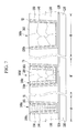
- FIG. 7 illustrates a cross-sectional view of a grain shape of the bulk layers formed in the trenches of the semiconductor device illustrated in FIG. 5 .
- third grains 163 may be generated in the third bulk layer 160 c , and an average grain size of the third grains 163 may be equal to or smaller than an average grain size of the first grains 161 of the first bulk layer 160 a formed in the first trench T 1 .
- Fourth grains 164 may be generated in the fourth bulk layer 160 d , and an average grain size of the fourth grains 164 may be larger than the average grain size of the third grains 163 .
- the average grain size of the fourth grains 164 may be equal to or smaller than an average grain size of the second grains 162 of the second bulk layer 160 b formed in the second trench T 2 .
- FIGS. 8 to 15 illustrate cross-sectional views of stages in a method of manufacturing a semiconductor device according to an exemplary embodiment.
- a trench lower layer 120 may be formed on a substrate 110 .
- the trench lower layer 120 may correspond to, e.g., a silicide layer, a source region, a drain region, or a gate insulating layer according to the type of contact structure or device to be formed.
- An insulating layer 130 (having a first trench T 1 and a second trench T 2 ) may be formed on the trench lower layer 120 by a chemical vapor depositing method or the like.
- an aspect ratio of the first trench T 1 may be larger than an aspect ratio of the second trench T 2 .
- the first trench T 1 and the second trench T 2 may be formed in a first region A and a second region B, respectively, and the first region A and the second region B may correspond to different regions of a system LSI. Accordingly, the degrees of integration of the regions A and B may be different from each other, and the first trench T 1 and the second trench T 2 formed in the first region A and the second region B, respectively, may have different aspect ratios.
- a barrier layer 140 may be formed on the insulating layer 130 so as to cover internal sides of the first trench T 1 and the second trench T 2 .
- the barrier layer 140 may be formed by, e.g., a chemical vapor depositing method, a sputtering method, or an atomic layer deposition method, and may be formed in a single layer or may also be formed in multiple layers by laminating a layer so as to include, e.g., titanium, tantalum, cobalt, a titanium nitride, a tantalum nitride, or a cobalt nitride.
- the barrier layer 140 is formed of titanium and a titanium nitride, the titanium and the titanium nitride may be formed by one process.
- the barrier layer 140 may help prevent a metal included in a seed layer or a bulk layer formed by a subsequent process from being dispersed to the substrate 110 or the insulating layer 130 .
- a seed layer 150 may be formed on the barrier layer 140 .
- the seed layer 150 may be conformally formed along lateral surfaces and lower surfaces of the internal sides of the first trench T 1 and the second trench T 2 , and may also be formed on an upper surface of the insulating layer 130 .
- the seed layer 150 may be formed of, e.g., copper, titanium, gold, silver, platinum, palladium, nickel, aluminum, rubidium, cobalt, or tungsten, or may also be formed of an alloy including at least one among them.
- the seed layer 150 may enable a bulk layer to be formed or facilitate the forming of a bulk layer in a subsequent process.
- a plasma treatment may be performed on the seed layer 150 .
- An exposed surface of the seed layer 150 may be plasma treated, and a first growth controlling region 150 a may be formed in the first region A along the surface of the seed layer 150 , and a second growth controlling region 150 b may be formed in the second region B along the surface of the seed layer 150 .
- an aspect ratio of the first trench T 1 may be larger than an aspect ratio of the second trench T 2 , and a width of the first trench T 1 may be smaller than a width of the second trench T 2 , so that intensity of the plasma treated on the surface of the seed layer 150 disposed in the first trench T 1 may be lower than intensity of the plasma treated on the surface of the seed layer 150 on the insulating layer 130 around the first trench T 1 and intensity of the plasma treated on the surface of the seed layer 150 of the second region B.
- the aspect ratio of the second trench T 2 may be smaller than the aspect ratio of the first trench T 1 and a width of the second trench T 2 may be relatively large, and the intensity of the plasma treated on the surface of the seed layer 150 disposed in the second trench T 2 may be substantially the same as the intensity of the plasma treated on the surface of the seed layer 150 on the insulating layer 130 around the first trench T 1 or on the insulating layer 130 around the second trench T 2 .
- the seed layers 150 formed in the first trench T 1 and the second trench T 2 which have different aspect ratios, may be simultaneously plasma-processed in the semiconductor device according to the present exemplary embodiment, so that, as illustrated in FIGS. 2 and 3 , growth controlling regions having different concentrations or different thicknesses may be formed in the seed layer 150 within the first trench T 1 and the seed layer 150 within the second trench T 2 .
- the first growth controlling region 150 a and the second growth controlling region 150 b may be formed on the surface of the seed layer 150 .
- the intensity of plasma may be increased or even though the intensity of plasma may have the same condition, when a thickness of the seed layer 150 is small, a space occupied by the growth controlling region distributed within the seed layer 150 may be increased.
- the first growth controlling region 150 a may be formed on or adjacent to only an upper portion of the insulating layer 130 in the first region A.
- the plasma may be rarely irradiated to the seed layer 150 within the first trench T 1 in the plasma treatment operation, or the intensity of plasma may be adjusted in the plasma treatment operation according to the increase in the aspect ratio of the first trench T 1 , so that the first growth controlling region 150 a may not be formed in the seed layer 150 within the first trench T 1 .
- a suitable plasma device may be used as a plasma device used in the plasma treatment operation, e.g., a remote plasma technology, in which plasma is generated in a region spaced apart from the substrate 110 , may be applied.
- the plasma treatment operation may be performed by using a nitrogen-containing gas, e.g., N 2 , N 2 H 4 , NH 3 , or a mixed gas thereof.
- a nitrogen-containing gas e.g., N 2 , N 2 H 4 , NH 3 , or a mixed gas thereof.
- the surface of the seed layer 150 before the plasma treatment may have an unstable energetic surface defect. Accordingly, activated atoms or ions, e.g., nitrogen atoms or nitrogen ions, may be bonded with the surface defect by the plasma to form dangling bonding, and thus it is possible to energetically stabilize the surface of the seed layer 150 .
- hydrogen atoms or hydrogen ions may be bonded with the surface of the seed layer 150 to form dangling bonding.
- the nitrogen-containing gas used in the plasma treatment operation may have a flow rate in a range, e.g., from 1 sccm to 50 sccm.
- the plasma treatment operation may be performed by using inactive or inter gas, e.g., argon gas, krypton gas, or xenon gas together, and the inactive gas may have a flow rate in a range from 1 sccm to 20 sccm.
- the plasma treatment operation may be performed under RF power in a range of 1 W to 2,000 W. Further, the plasma treatment operation may be performed without applying bias power.
- a process temperature of the plasma treatment operation may be in a range of ⁇ 50° C. to 250° C., and pressure may be 8 mTorr or less.
- plasma may be irradiated to the seed layer 150 disposed within the trenches having different aspect ratios, e.g., different widths, so that even though the plasma under the same condition is treated, the plasma with different intensities may be irradiated according to the position of the seed layer 150 .
- the first growth controlling region 150 a may be formed on or adjacent to the insulating layer 130 in a first region A 1 to suppress the growth of a bulk layer to be described below, and the first growth controlling region 150 a , which has a relatively low concentration or small thickness, may be formed on the seed layer 150 within the first trench T 1 or the first growth controlling region 150 a may not be formed, so that the bulk layer may be first grown from the surface of the seed layer 150 disposed in the lower portion of the first trench T 1 .
- a first bulk layer 160 a may be formed on the seed layer 150 .
- the first bulk layer 160 a may use at least one of various tungsten contained gas including, e.g., WF 6 , WCl 6 , and W(CO) 6 , and may be formed by using at least one of reducing agents including, e.g., silane (SiH 4 ), disilane (Si 2 H 6 ), hydrazine (N 2 H), diborane (B 2 H 6 ), and germanes (GeH 4 ).
- the first bulk layer 160 a may be formed of the same material as that of the seed layer 150 .
- the first bulk layer 160 a may be include copper, titanium, gold, silver, platinum, palladium, nickel, aluminum, rubidium, cobalt, tungsten, or an alloy thereof.
- the seed layer 150 in the lower portion of the second trench T 2 may be in an energetically stable state by the second growth controlling region 150 b , so that the first bulk layer 160 a may not be formed in the second trench T 2 . Further, in the first trench T 1 , the growth of the first bulk layer 160 a may begin from the surface of the seed layer 150 disposed in the lower portion of the first trench T 1 .
- the first bulk layer 160 a may be grown from the lower portion of the first trench T 1 and may be filled in the first trench T 1 , so that the first trench T 1 may be completely filled with the first bulk layer 160 a as illustrated in FIG. 14 without a seam or a void.
- a first process temperature in the operation of forming the first bulk layer 160 a may have a range of about 200° C. to 400° C.
- the first bulk layer 160 a may be formed only within the first trench T 1 . In an implementation, the first bulk layer 160 a may be slightly formed within the second trench T 2 .
- a second bulk layer 160 b may be formed on the first bulk layer 160 a and the seed layer 150 .
- the second bulk layer 160 b may be formed of the same material as that of the first bulk layer 160 a .
- a second process temperature for forming the second bulk layer 160 b may be higher than the aforementioned first process temperature of the first bulk layer 160 a .
- the second growth controlling region 150 b (suppressing formation of the second bulk layer 160 b ) may be on the surface of the seed layer 150 disposed in the lower portion of the second trench T 2 , and a growth rate may be increased by increasing the second process temperature.
- an average grain size of the second bulk layer 160 b may be larger than an average grain size of the first bulk layer 160 a .
- the second process temperature may have a range of about 250° C. to 450° C.
- the second bulk layer 160 b may be formed even on the first bulk layer 160 a filled in the first trench T 1 .
- the first region A may have a structure, in which the second bulk layer 160 b having the larger average grain size is disposed on the first bulk layer 160 a .
- the planarization process may be performed so that the upper surface of the insulating layer 130 is exposed.
- the planarization process may use a CMP process or an etch back process.
- FIGS. 16 to 19 illustrate cross-sectional views of stages in a modified example of the method of manufacturing the semiconductor device described in FIGS. 8 to 15 .
- a method of manufacturing a semiconductor device may further include a method of manufacturing a filled structure of a third trench T 3 in a third region B′.
- the exemplary embodiment described with reference to FIGS. 8 to 15 represents the method of manufacturing the trench filled structure in the first and second regions A and B, but in the present exemplary embodiment, the method may further include a method of manufacturing a structure related to the third region B′, other than or different from the first and second regions A and B.
- a barrier layer 140 and a seed layer 150 may be formed within a third trench T 3 in the third region B′, similar to a first trench T 1 and a second trench T 2 , as illustrated in FIG. 16 , by performing the same process as the operations described with reference to FIGS. 8 to 12 .
- An aspect ratio of the third trench 13 may be smaller than an aspect ratio of the first trench T 1 and may be larger than an aspect ratio of the second trench T 2 .
- a width of the third trench T 3 may be larger than a width of the first trench T 1 and may be smaller than a width of the second trench T 2 .
- a third growth controlling region 150 c may be formed in the third region B′ as illustrated in FIG. 16 , and as described in the exemplary embodiment of the structure of FIG. 6 , an average concentration or an average thickness of the third growth controlling region 150 c may be different from the average concentrations or the average thicknesses of the first and second growth controlling regions 150 a and 150 b .
- a thickness of a third bulk layer 160 c which is described below, formed in the third trench T 3 may be small, and when the plasma for the treatment is weak, a thickness of the third bulk layer 160 c may be large.
- a thickness of the third bulk layer 160 c may be small by controlling the intensity of plasma for the treatment to be large, and then, a thickness of a fourth bulk layer 160 d , which is illustrated in FIG. 6 , formed on the third bulk layer 160 c may be formed to be relatively large.
- a thickness of the third bulk layer 160 c may also be formed to be relatively larger than that of the fourth bulk layer 160 d unlike the illustration of FIG. 6 by controlling the intensity of plasma for the treatment to be small.
- the first bulk layer 160 a may be formed on the seed layer 150 within the first trench T 1
- the third bulk layer 160 c may be formed on the seed layer 150 of the third trench T 3 .
- the growth of the first bulk layer 160 a may begin from the surface of the seed layer 150 in the lower portion of the first trench T 1 .
- the third bulk layer 160 c may be grown from the surface of the seed layer 150 in a lower portion of the second trench T 2 .
- the seed layer 150 in a lower portion of the second trench T 2 may be in an energetically stable state by the second growth controlling region 150 b , so that the first bulk layer 160 a or the third bulk layer 160 c may not be formed in the second trench T 2 .
- the degree of stabilization of the seed layer 150 may be different for each region by a difference in an average concentration or an average thickness of the first growth controlling region 150 a , the second growth controlling region 150 b , and the third growth controlling region 150 c . Accordingly, even though the bulk layer is formed on the seed layer 150 under the same process condition, the first bulk layer 160 a may be formed in the first region A while being completely filled in the first trench T 1 , the bulk layer may not be formed in the second region B in the present operation, and the third bulk layer 160 c may be conformally formed on the seed layer 150 of the third trench T 3 in the third region B′. Referring to FIG. 18 as the modified exemplary embodiment of the conformally formed third bulk layer 160 c , the third bulk layer 160 c may be relatively thin in a side portion of the third trench T 3 and may be relatively thick in a lower portion of the third trench T 3 .
- the first bulk layer 160 a and the third bulk layer 160 c may be simultaneously formed, and may be formed of the same material. As illustrated in FIG. 7 , an average grain size of third grains 163 of the third bulk layer 160 c may be equal to or smaller than an average grain size of first grains 161 of the first bulk layer 160 a.
- a first process temperature in the operation of forming the first bulk layer 160 a and the third bulk layer 160 c may have a range of about 200° C. to 400° C.
- the first bulk layer 160 a and the third bulk layer 160 c may not be formed within the second trench T 2 at all as illustrated in FIGS. 17 and 18 , or the material forming the first bulk layer 160 a and the third bulk layer 160 c may also be slightly formed within the second trench T 2 .
- a second bulk layer 160 b may be formed on the first bulk layer 160 a , the third bulk layer 160 c , and the seed layer 150 .
- the second bulk layer 160 b may be formed of the same material as that of the first bulk layer 160 a and the third bulk layer 160 c .
- a second process temperature for forming the second bulk layer 160 b may be higher than the aforementioned first process temperature of the first bulk layer 160 a .
- the second growth controlling region 150 b suppressing the second bulk layer 160 b from being formed may be formed on the surface of the seed layer 150 disposed in the second trench T 2 , so that it may be difficult to form the second bulk layer 160 b under the same condition as that when the first bulk layer 160 a and the third bulk layer 160 c are formed. Accordingly, a growth rate may be increased by increasing the second process temperature, and as a result, as illustrated in FIG. 7 , the second bulk layer 160 b may be formed so that a grain size of the second bulk layer 160 b may be larger than an average grain size of the first bulk layer 160 a and the third bulk layer 160 c.
- the second bulk layer 160 b may be completely filled in the third trench T 3 (e.g., may completely fill remaining portions of the third trench T 3 ).
- the second bulk layer 160 b may also be formed on the first bulk layer 160 a filled in the first trench T 1 .
- a structure, in which the second bulk layer 160 b having the larger average grain size than that of the first bulk layer 160 a is disposed on the first bulk layer 160 a may be present in the first region A
- a structure, in which the second bulk layer 160 b having the larger average grain size than that of the third bulk layer 160 c is disposed on the third bulk layer 160 c may be present in the third region B′.
- a planarization process may be performed after the second bulk layer 160 b is formed, and thus the second bulk layer 160 b in the first region A may be removed, and the second bulk layer 160 b corresponding to a part left after being filled in the third trench T 3 in the second region B may be removed (e.g., portions outside of the third trench T 3 may be removed).
- the planarization process may be performed so that the upper surface of the insulating layer 130 is exposed, and when the planarization process is performed as described above, it is possible to form a trench filled structure of the semiconductor device according to the exemplary embodiment illustrated in FIG. 6 .
- FIG. 20 illustrates a block diagram schematically showing a semiconductor device according to an exemplary embodiment.
- a semiconductor device 1000 may be a system LSI, e.g., an application processor (AP), including an SRAM formed region 500 and a logic region 600 .
- a first transistor 511 and a third transistor 512 may be disposed in the SRAM formed region 500
- a second transistor 611 and a fourth transistor 612 may be disposed in the logic region 600 .
- the degree of integration of the SRAM formed region 500 may be relatively larger than the degree of integration of the logic region 600 .
- FIG. 20 illustratively shows the SRAM formed region 500 and the logic region 600 .
- the exemplary embodiments according to the present disclosure may be applied to a passive device region or an input/output pad forming region, instead of the logic region 600 , in the system LSI, and a region, e.g., DRAM, MRAM, RRAM, and PRAM formed regions, in which different types of devices corresponding to a memory device, are formed, instead of the SRAM formed region 500 .
- a region e.g., DRAM, MRAM, RRAM, and PRAM formed regions, in which different types of devices corresponding to a memory device, are formed, instead of the SRAM formed region 500 .
- FIG. 21 illustrates a cross-sectional view schematically showing a gate according to an exemplary embodiment.
- a device isolating pattern 205 limiting an active region of a substrate 110 may be formed.
- the substrate 110 may be, e.g., a bulk silicon substrate, silicon (SOI) on an insulating layer, a silicon substrate, or a substrate, in which an epilayer is formed on a base substrate as described with reference to FIG. 1 .
- SOI silicon
- a source region 220 and a drain region 230 may be formed in the substrate 110 .
- a gate insulating layer 210 may be disposed on the substrate 110 .
- the gate insulating layer 210 may include a high-dielectric layer having a high dielectric constant.
- the gate insulating layer 210 may include at least one of a metal oxide and a metal-semiconductor-oxygen compound layer.
- the metal oxide may be, e.g., a hafnium oxide layer or a zirconium oxide
- the metal-semiconductor-oxygen compound layer may be, e.g., a hafnium-silicon-oxygen-nitrogen compound.
- An insulating layer 130 which has a first trench T 1 and a second trench T 2 overlapping the gate insulating layer 210 , may be disposed on the substrate 110 .
- a barrier layer 140 may be conformally formed in the first trench T 1 and the second trench T 2 , and a gate spacer 240 is formed between the insulating layer 130 and the barrier layer 140 .
- the source region 220 and the drain region 230 may be formed in an LDD structure by using the gate spacer 240 .
- a seed layer 150 may be disposed on the barrier layer 140 .
- a first growth controlling region 150 a and a second growth controlling region 150 b may be formed in the seed layer 150 .
- a first metal gate electrode 160 a filled in the first trench T 1 may be formed on the seed layer 150
- a second metal gate electrode 160 b filled in the second trench T 2 may be formed on the seed layer 150 .
- the first metal gate electrode 160 a and the second metal gate electrode 160 b may correspond to the first bulk layer 160 a and the second bulk layer 160 b descried with reference to FIG. 1 , respectively.
- an aspect ratio of the first trench T 1 in which a gate of a first transistor 511 is formed, may be larger than an aspect ratio of the second trench T 2 , in which a gate of a second transistor 611 is formed.
- an average concentration or an average thickness of the first growth controlling region 150 a may be different from an average concentration or an average thickness of the second growth controlling region 150 b , and all of the descriptions of the trench filled structure according to the exemplary embodiment may be applied to the present exemplary embodiment.
- the exemplary embodiment of FIG. 21 represents an example, in which the trench filled structure is applied to the gate.
- FIG. 22 illustrates a cross-sectional view schematically showing source and drain contact structures in a transistor according to an exemplary embodiment.
- a source region 350 and a drain region 360 may be formed in a substrate 110 , and a gate insulating layer 310 may be disposed on an active region of the substrate 110 .
- a gate electrode 320 may be disposed on the gate insulating layer 310 , and a metal oxide silicide layer 330 may be disposed on the gate electrode 320 .
- a spacer 340 may be disposed on a lateral surface of a gate structure including the gate insulating layer 310 , the gate electrode 320 , and the metal oxide silicide layer 330 , and the spacer 340 may be formed by using a silicon nitride, a silicon oxynitride, or a titanium oxynitride.
- An insulating layer 130 covering the gate structure may be disposed on the substrate 110 .
- the insulating layer 130 may have a first trench T 1 and a second trench T 2 .
- a barrier layer 140 may be conformally formed in the first trench T 1 and the second trench T 2 , and a seed layer 150 may be disposed on the barrier layer 140 .
- a first growth controlling region 150 a and a second growth controlling region 150 b may be formed in the seed layer 150 .
- a first bulk layer 160 a filled in the first trench T 1 may be formed on the seed layer 150
- a second bulk layer 160 b filled in the second trench T 2 may be formed on the seed layer 150 .
- an aspect ratio of the first trench T 1 in a contact structure of the source region 350 and the drain region 360 of a third transistor 512 may be larger than an aspect ratio of the second trench T 2 in a contact structure of the source region 350 and the drain region 360 of a fourth transistor 612 .
- an average concentration or an average thickness of the first growth controlling region 150 a may be different from an average concentration or an average thickness of the second growth controlling region 150 b , and all of the descriptions of the trench filled structure according to the exemplary embodiment may be applied to the present exemplary embodiment.
- the exemplary embodiment of FIG. 22 represents an example in which the trench filled structure is applied to the contact structure of the source region and the drain region.
- a semiconductor device 1000 according to a modified exemplary embodiment of the exemplary embodiment of FIGS. 20 to 22 may have a trench structure in which a plurality of transistors disposed within an SRAM formed region 500 have different aspect ratios, or a trench structure in which a plurality of transistors disposed within a logic region 600 have different aspect ratios.
- a semiconductor device may be highly integrated, and thus the semiconductor device may be miniaturized. Accordingly, in order to form a contact conductive layer, various issues may arise due to a lack of a process margin during a process of depositing a conductive material in a micro pattern, so that it may be gradually difficult to implement the semiconductor device. In order to satisfy the demands for the high integration of the semiconductor device, various researches have been conducted.
- an aspect ratio of a contact part for an interconnection may be increased by the high integration of the semiconductor device, so that a seam and/or a void may be generated.
- a plasma treatment is performed during a process of forming a bulk layer in trenches having different aspect ratios, thereby preventing a seam and/or a void from being generated in the bulk layer.
- T 1 , T 2 , T 3 , T 4 Trench
Landscapes
- Engineering & Computer Science (AREA)
- Physics & Mathematics (AREA)
- Computer Hardware Design (AREA)
- Condensed Matter Physics & Semiconductors (AREA)
- General Physics & Mathematics (AREA)
- Microelectronics & Electronic Packaging (AREA)
- Power Engineering (AREA)
- Manufacturing & Machinery (AREA)
- Plasma & Fusion (AREA)
- Electrodes Of Semiconductors (AREA)
- Semiconductor Memories (AREA)
- Geometry (AREA)
- Internal Circuitry In Semiconductor Integrated Circuit Devices (AREA)
Abstract
A semiconductor device and a method of manufacturing the same, the semiconductor device including a substrate; an insulating layer on the substrate, the insulating layer including a first trench and a second trench therein, the second trench having an aspect ratio that is smaller than an aspect ratio of the first trench; a barrier layer in the first trench and the second trench; a seed layer on the barrier layer in the first trench and the second trench; a first bulk layer on the seed layer and filled in the first trench; and a second bulk layer on the seed layer and filled in the second trench, wherein an average grain size of the second bulk layer is larger than an average grain size of the first bulk layer.
Description
Korean Patent Application No. 10-2016-0114022, filed on Sep. 5, 2016, in the Korean Intellectual Property Office, and entitled: “Semiconductor Device and Method of Manufacturing the Same,” is incorporated by reference herein in its entirety.
Embodiments relate to a semiconductor device and a method of manufacturing the same.
A semiconductor device has characteristics, such as a small size, a multi-function, and/or low manufacturing cost, so that the semiconductor device may be used in many electronic industries. The semiconductor device may include a memory device storing data, a logic device calculating and processing data, a hybrid device, which is capable of simultaneously performing various functions, and the like.
The above information disclosed in this Background section is only for enhancement of understanding of the background of the invention and therefore it may contain information that does not form the prior art that is already known in this country to a person of ordinary skill in the art.
The embodiments may be realized by providing a semiconductor device including a substrate; an insulating layer on the substrate, the insulating layer including a first trench and a second trench therein, the second trench having an aspect ratio that is smaller than an aspect ratio of the first trench; a barrier layer in the first trench and the second trench; a seed layer on the barrier layer in the first trench and the second trench; a first bulk layer on the seed layer and filled in the first trench; and a second bulk layer on the seed layer and filled in the second trench, wherein an average grain size of the second bulk layer is larger than an average grain size of the first bulk layer.
The embodiments may be realized by providing a semiconductor device including a substrate; an insulating layer on the substrate, the insulating layer having a first trench and a second trench, the second trench having an aspect ratio that is smaller than an aspect ratio of the first trench; a barrier layer in the first trench and the second trench; a first seed layer in the first trench and a second seed layer in the second trench, the first seed layer and the second seed layer being on the barrier layer in the first trench and the second trench; a first bulk layer on the first seed layer and filled in the first trench; and a second bulk layer on the second seed layer and filled in the second trench, wherein the first seed layer includes a first growth controlling region including a plasma material and the second seed layer includes a second growth controlling region including a plasma material, and an average concentration of plasma material included in the first growth controlling region is smaller than an average concentration of plasma material included in the second growth controlling region, or an average thickness of the first growth controlling region is less than an average thickness of the second growth controlling region.
The embodiments may be realized by providing a method of manufacturing a semiconductor device, the method including forming an insulating layer having a first trench and a second trench on a substrate such that the second trench has an aspect ratio that is smaller than an aspect ratio of the first trench; forming a barrier layer to cover the first trench and the second trench; forming a seed layer in the first trench and the second trench to cover the barrier layer; plasma-treating the seed layer; forming a first bulk layer in the first trench; and forming a second bulk layer in the second trench, wherein a process temperature of the forming of the second bulk layer is higher than a process temperature of the forming of the first bulk layer.
The embodiments may be realized by providing a semiconductor device including a substrate; an insulating layer on the substrate, the insulating layer having a first trench and a second trench, the second trench having an aspect ratio that is smaller than an aspect ratio of the first trench; a barrier layer in the first trench and the second trench; a first seed layer in the first trench and a second seed layer in the second trench, the first seed layer and the second seed layer being on the barrier layer in the first trench and the second trench; a first bulk layer on the first seed layer and filling in the first trench; and a second bulk layer on the second seed layer and filling in the second trench, wherein an average grain size of the second bulk layer is larger than an average grain size of the first bulk layer.
Features will be apparent to those of skill in the art by describing in detail exemplary embodiments with reference to the attached drawings in which:
Hereinafter, a trench filled structure in a semiconductor device according to an exemplary embodiment of the present disclosure will be described with reference to FIG. 1 .
Referring to FIG. 1 , a trench lower layer 120 may be disposed on a substrate 110. In an implementation, the substrate 110 may be a bulk silicon substrate or a silicon (SOI) substrate on an insulating layer. In an implementation, the substrate 110 may be a silicon substrate, or may also be a substrate, in which an epi layer is formed on a base substrate. The trench lower layer 120 may be a silicide layer, a source region, a drain region, or a gate insulating layer. When the trench lower layer 120 is a silicide layer, a wiring formed in the substrate 110 may be connected to a trench filled structure, when the trench lower layer 120 is a source and/or drain region, the trench filled structure may form a contact structure with the source region and the drain region, and when the trench lower layer 120 is a gate insulating layer, the trench filled structure may form a gate.
An insulating layer 130 (having a first trench T1 and a second trench T2) may be disposed on the trench lower layer 120. In an implementation, as illustrated in FIG. 1 , the insulating layer 130 may be a single layer, or may be formed in multiple layers. The insulating layer 130 may be formed by a chemical vapor depositing method.
In the present exemplary embodiment, an aspect ratio of the first trench T1 may be larger than an aspect ratio of the second trench T2. In the present exemplary embodiment, the aspect ratio may be defined by a width of an inlet of the trench:a depth of the trench.
The first trench T1 and the second trench T2 may be formed in a first region A and a second region B, respectively. The first region A and the second region B indicate different regions in a semiconductor system. The present exemplary embodiment may represent the trench filled structure in the semiconductor device disposed in each of the first region A and the second region B.
A barrier layer 140 may be conformally formed within the first trench T1 and the second trench T2. The barrier layer 140 may include, e.g., titanium, tantalum, cobalt, titanium, a nitride, a tantalum nitride, or a cobalt nitride. In an implementation, the barrier layer 140 may be formed of multiple layers formed of respective layers including a combination of the aforementioned materials. In this case, a combined material of each layer may be different for each layer.
A seed layer 150 may be disposed on the barrier layer 140. The seed layer 150 may be conformally formed along lateral surfaces and lower surfaces of the first trench T1 and the second trench T2.
The seed layer 150 may be formed of, e.g., copper, titanium, gold, silver, platinum, palladium, nickel, aluminum, rubidium, cobalt, or tungsten, or an alloy including at least one among them.
A growth controlling region may be disposed on a surface of the seed layer 150. The growth controlling region may be a region formed by a plasma treatment, which will be described in a manufacturing method to be described below.
The seed layer 150 in the first trench T1 may be a first seed layer and the seed layer 150 in the second trench T2 may be a second seed layer. The first seed layer may include a first growth controlling region 150 a including a plasma material, and the second seed layer may include a second growth controlling region 150 b including a plasma material. Each of the first growth controlling region 150 a and the second growth controlling region 150 b may be disposed on a surface of the seed layer 150. For example, a concentration of plasma material included in the seed layer 150 may be decreased from the surface of the seed layer 150 to the barrier layer 140. For example, a concentration of plasma material in a region of the seed layer 150 adjacent to the barrier layer may be less than a concentration of plasma material in the growth controlling region distal to the barrier layer 140.
A concentration of the plasma material included in the seed layer 150 disposed at a side portion of the first trench T1 may be larger than a concentration of a plasma material included in the seed layer 150 disposed under or at a bottom of the first trench T1 (e.g., adjacent to the trench lower layer 120). Similarly, a concentration of the plasma material included in the seed layer 150 disposed at a side portion of the second trench T2 may be larger than a concentration of a plasma material included in the seed layer 150 disposed under or at a bottom of the second trench T2.
In an implementation, a thickness of the first growth controlling region 150 a disposed in the side portion of the first trench T1 may be larger than a thickness of the first growth controlling region 150 a disposed under the first trench T1. Similarly, a thickness of the second growth controlling region 150 b disposed in the side portion of the second trench T2 may be larger than a thickness of the second growth controlling region 150 b disposed under the second trench T2.
As a modified exemplary embodiment, each of the first and second growth controlling regions 150 a and 150 b may be formed in a most region of the seed layer 150 (e.g., a majority of the seed layer 150 may be made of the first and second growth controlling regions 150 a and 150 b). In such a case, the concentration of the plasma material included in each of the first and second growth controlling regions 150 a and 150 b may still be decreased from the surface of the seed layer 150 to the barrier layer 140.
In an implementation, the first growth controlling region 150 a may be formed within the first trench T1. In an implementation, plasma may be rarely or slightly irradiated to the seed layer 150 within the first trench T1 (in the plasma treatment operation of the manufacturing method to be described below) according or due to an increase in the aspect ratio of the first trench T1, and the first growth controlling region 150 a may not be formed. For example, the first growth controlling region 150 a may be formed only on the insulating layer 130. In an implementation, the first growth controlling region disposed on the insulating layer 130 may be extended and the first growth controlling region 150 a may be formed at a part of the side portion of the first trench T1.
In an implementation, an average concentration or an average thickness of the first growth controlling region 150 a may be different from an average concentration or an average thickness of the second growth controlling region 150 b. This will be described with reference to FIGS. 2 and 3 .
Referring to FIG. 2 , a (e.g., plasma) concentration of the first growth controlling region 150 a disposed under or at a bottom of the first trench T1 may be smaller than a concentration of the second growth controlling region 150 b disposed under or at a bottom of the second trench T2. In an implementation, when a concentration of the first growth controlling region 150 a disposed in the side portion of the first trench T1 is compared with a concentration of the second growth controlling region 150 b disposed in the side portion of the second trench T2 (disposed in correspondence with the first growth controlling region 150 a, e.g., at a similar location), the concentration of the first growth controlling region 150 a may be smaller than the concentration of the second growth controlling region 150 b.
The concentration of each of the first growth controlling region 150 a and the second growth controlling region 150 b may be different according to a position within the first trench T1 and the second trench T2. An average concentration of the plasma material included in the first growth controlling region 150 a disposed in the first trench T1 may be smaller than an average concentration of the plasma material included in the second growth controlling region 150 b disposed in the second trench T2.
Referring to FIG. 3 , a thickness of the first growth controlling region 150 a disposed under or at a bottom of the first trench T1 may be smaller than an average thickness of the second growth controlling region 150 b disposed in a second region B disposed in a lower portion or bottom of the second trench T2. In an implementation, when a thickness of the first growth controlling region 150 a disposed in the side portion of the first trench T1 is compared with a thickness of the second growth controlling region 150 b disposed in the side portion of the second trench T2 (disposed in correspondence with the first growth controlling region 150 a, e.g., at a similar location), the thickness of the first growth controlling region 150 a may be smaller than the thickness of the second growth controlling region 150 b.
The thickness of each of the first growth controlling region 150 a and the second growth controlling region 150 b may be different according to a position within the first trench T1 and the second trench T2. An average thickness of the first growth controlling region 150 a disposed in the first trench T1 may be smaller than an average thickness of the second growth controlling region 150 b disposed in the second trench T2.
In FIGS. 2 and 3 , the concentrations and the thicknesses of the first and second growth controlling regions 150 a and 150 b are separately described. An average thickness of the first growth controlling region 150 a disposed in the first trench T1 may be smaller than an average thickness of the second growth controlling region 150 b disposed in the second trench T2 and an average (e.g., plasma) concentration of the first growth controlling region 150 a disposed in the first trench T1 may be smaller than an average concentration of the second growth controlling region 150 b disposed in the second trench T2.
Referring back to FIG. 1 , a bulk layer may be disposed on the seed layer 150. The bulk layer may include a first bulk layer 160 a disposed in a first region A and a second bulk layer 160 a disposed in the second region B. The first bulk layer 160 a and the second bulk layer 160 b may be completely filled in (e.g., remaining portions of) the first trench T1 and the second trench T2, respectively. In an implementation, as illustrated in FIG. 1 , the first bulk layer 160 a may not be formed within the second trench T2. In an implementation, the first bulk layer 160 a may be slightly formed within the second trench T2.
In an implementation, the first and second bulk layers 160 a and 160 b may each independently include, e.g., copper, titanium, gold, silver, platinum, palladium, nickel, aluminum, rubidium, cobalt, tungsten, or an alloy thereof.
In an implementation, an average grain size of a material of the first bulk layer 160 a may be smaller than an average grain size of a material of the second bulk layer 160 b. This will be described with reference to FIG. 4 .
Referring to FIG. 4 , first grains 161 may be generated in the first bulk layer 160 a, and an average grain size of the first grains 161 may be smaller than a width of the first trench T1. Second grains 162 may be generated in the second bulk layer 160 b, and an average grain size of the second grains 162 may be larger than the average grain size of the first grains 161.
In an implementation, each of the first bulk layer 160 a and the second bulk layer 160 b according to the present exemplary embodiment may be formed of, e.g., tungsten. In an implementation, as described above, the first bulk layer 160 a and the second bulk layer 160 b may be formed of the same material. In an implementation, the first bulk layer 160 a and the second bulk layer 160 b may include different materials.
In the present exemplary embodiment, the plasma may be processed on the trenches T1 and T2 having the different aspect ratios (as described in the manufacturing method to be described below), the first bulk layer 160 a may be sequentially formed in the first trench T1 having a relatively small width from a bottom of the first trench T1 in an up direction (e.g., away from the substrate 110), so that it is possible to help prevent a seam or a void from being generated. The second bulk layer 160 b may be separately formed in the second trench T2 (having a relatively large width), and the average grain sizes of the first bulk layer 160 a and the second bulk layer 160 b may be different from each other.
Referring to FIG. 5 , the semiconductor device according to the present exemplary embodiment may further include a structure of a filled third trench T3 formed in a third region B′. For example, the exemplary embodiment described with reference to FIG. 1 represents the trench filing structure in the first and second regions A and B. In the present exemplary embodiment, the semiconductor device may further include a trench filled structure disposed in the third region B′, other than or different from the first and second regions A and B. Hereinafter, only the different matters from those of the exemplary embodiment of FIG. 1 will be described.
Referring to FIG. 5 , a barrier layer 140 may be conformally formed within a third trench T3 in the third region B′. A seed layer 150 including a third growth controlling region 150 c may be disposed on the barrier layer 140, and a third bulk layer 160 c and a fourth bulk layer 160 d may be sequentially disposed on the seed layer 150.
An aspect ratio of the third trench T3 according to the present exemplary embodiment may be smaller than an aspect ratio of a first trench T1 and may be larger than an aspect ratio of the second trench T2.
When the seed layer 150 disposed within the third trench T3 is referred to as a third seed layer, the third seed layer may include the third growth controlling region 150 c including a plasma material. The third growth controlling region 150 c may be disposed on or at a surface of the seed layer 150, and a concentration of the plasma included in the third growth controlling region 150 c may be decreased from the surface of the seed layer 150 to the barrier layer 140. In an implementation, the third growth controlling region 150 c may be formed in the most region of the seed layer 150 (e.g., the majority of the seed layer 150 may be made up of the third growth controlling region 150 c), and the concentration of the plasma material included in the third growth controlling region 150 c may be decreased from the surface of the seed layer 150 to the barrier layer 140.
In an implementation, an average concentration or an average thickness of the third growth controlling region 150 c may be different from average concentrations or the average thicknesses of first and second growth controlling regions 150 a and 150 b. In an implementation, an average concentration of the plasma material included in the third growth controlling region 150 c may be larger than an average concentration of the plasma material included in the first growth controlling region 150 a and may be smaller than an average concentration of the plasma material included in the second growth controlling region 150 b. In an implementation, an average thickness of the third growth controlling region 150 c may be larger than an average thickness of the first growth controlling region 150 a and may be smaller than an average thickness of the second growth controlling region 150 b.
The third bulk layer 160 c may be disposed on the seed layer 150 in the third region B′. The third bulk layer 160 c may be conformally formed along the surface of the seed layer 150. The third bulk layer 160 c may be simultaneously formed with the first bulk layer 160 a in the first region A. In an implementation, different from the conformally formed third bulk layer 160 c in FIG. 5 , referring to FIG. 6 as a modified exemplary embodiment, the third bulk layer 160 c may be formed to be relatively thin in a side portion of the third trench T3 and to be relatively thick in a lower portion of the third trench T3.
A fourth bulk layer 160 d may be disposed on the third bulk layer 160 c. The fourth bulk layer 160 d may be completely filled in the third trench T3 (e.g., may fill remaining portions of the third trench T3). The fourth bulk layer 160 d may be simultaneously formed with the second bulk layer 160 b in the second region B.
In an implementation, as illustrated in FIGS. 5 and 6 , the first bulk layer 160 a and the third bulk layer 160 c may not be formed within the second trench T2 at all. In an implementation, the material forming the first bulk layer 160 a and the third bulk layer 160 c may also be slightly formed within the second trench T2.
In the present exemplary embodiment, an average grain size of a material of the third bulk layer 160 c may be smaller than an average grain size of a material of the fourth bulk layer 160 d. This will be described with reference to FIG. 7 .
Referring to FIG. 7 , third grains 163 may be generated in the third bulk layer 160 c, and an average grain size of the third grains 163 may be equal to or smaller than an average grain size of the first grains 161 of the first bulk layer 160 a formed in the first trench T1. Fourth grains 164 may be generated in the fourth bulk layer 160 d, and an average grain size of the fourth grains 164 may be larger than the average grain size of the third grains 163. The average grain size of the fourth grains 164 may be equal to or smaller than an average grain size of the second grains 162 of the second bulk layer 160 b formed in the second trench T2.
In addition to the difference described above, all of the contents described with reference to FIGS. 1 to 4 may be applied to the present exemplary embodiment.
Hereinafter, an example of a method of manufacturing the semiconductor device according to the exemplary embodiment will be described.
Referring to FIG. 8 , a trench lower layer 120 may be formed on a substrate 110.
The trench lower layer 120 may correspond to, e.g., a silicide layer, a source region, a drain region, or a gate insulating layer according to the type of contact structure or device to be formed.
An insulating layer 130 (having a first trench T1 and a second trench T2) may be formed on the trench lower layer 120 by a chemical vapor depositing method or the like. For example, an aspect ratio of the first trench T1 may be larger than an aspect ratio of the second trench T2. The first trench T1 and the second trench T2 may be formed in a first region A and a second region B, respectively, and the first region A and the second region B may correspond to different regions of a system LSI. Accordingly, the degrees of integration of the regions A and B may be different from each other, and the first trench T1 and the second trench T2 formed in the first region A and the second region B, respectively, may have different aspect ratios.
Referring to FIG. 9 , a barrier layer 140 may be formed on the insulating layer 130 so as to cover internal sides of the first trench T1 and the second trench T2.
The barrier layer 140 may be formed by, e.g., a chemical vapor depositing method, a sputtering method, or an atomic layer deposition method, and may be formed in a single layer or may also be formed in multiple layers by laminating a layer so as to include, e.g., titanium, tantalum, cobalt, a titanium nitride, a tantalum nitride, or a cobalt nitride. When the barrier layer 140 is formed of titanium and a titanium nitride, the titanium and the titanium nitride may be formed by one process.
The barrier layer 140 may help prevent a metal included in a seed layer or a bulk layer formed by a subsequent process from being dispersed to the substrate 110 or the insulating layer 130.
Referring to FIG. 10 , a seed layer 150 may be formed on the barrier layer 140.
The seed layer 150 may be conformally formed along lateral surfaces and lower surfaces of the internal sides of the first trench T1 and the second trench T2, and may also be formed on an upper surface of the insulating layer 130.
The seed layer 150 may be formed of, e.g., copper, titanium, gold, silver, platinum, palladium, nickel, aluminum, rubidium, cobalt, or tungsten, or may also be formed of an alloy including at least one among them. The seed layer 150 may enable a bulk layer to be formed or facilitate the forming of a bulk layer in a subsequent process.
Referring to FIG. 11 , a plasma treatment may be performed on the seed layer 150.
An exposed surface of the seed layer 150 may be plasma treated, and a first growth controlling region 150 a may be formed in the first region A along the surface of the seed layer 150, and a second growth controlling region 150 b may be formed in the second region B along the surface of the seed layer 150. For example, an aspect ratio of the first trench T1 may be larger than an aspect ratio of the second trench T2, and a width of the first trench T1 may be smaller than a width of the second trench T2, so that intensity of the plasma treated on the surface of the seed layer 150 disposed in the first trench T1 may be lower than intensity of the plasma treated on the surface of the seed layer 150 on the insulating layer 130 around the first trench T1 and intensity of the plasma treated on the surface of the seed layer 150 of the second region B.
In an implementation, the aspect ratio of the second trench T2 may be smaller than the aspect ratio of the first trench T1 and a width of the second trench T2 may be relatively large, and the intensity of the plasma treated on the surface of the seed layer 150 disposed in the second trench T2 may be substantially the same as the intensity of the plasma treated on the surface of the seed layer 150 on the insulating layer 130 around the first trench T1 or on the insulating layer 130 around the second trench T2.
As descried above, the seed layers 150 formed in the first trench T1 and the second trench T2, which have different aspect ratios, may be simultaneously plasma-processed in the semiconductor device according to the present exemplary embodiment, so that, as illustrated in FIGS. 2 and 3 , growth controlling regions having different concentrations or different thicknesses may be formed in the seed layer 150 within the first trench T1 and the seed layer 150 within the second trench T2.
In an implementation, the first growth controlling region 150 a and the second growth controlling region 150 b may be formed on the surface of the seed layer 150. For example, even though the intensity of plasma may be increased or even though the intensity of plasma may have the same condition, when a thickness of the seed layer 150 is small, a space occupied by the growth controlling region distributed within the seed layer 150 may be increased.
As illustrated in FIG. 12 , the first growth controlling region 150 a may be formed on or adjacent to only an upper portion of the insulating layer 130 in the first region A. The plasma may be rarely irradiated to the seed layer 150 within the first trench T1 in the plasma treatment operation, or the intensity of plasma may be adjusted in the plasma treatment operation according to the increase in the aspect ratio of the first trench T1, so that the first growth controlling region 150 a may not be formed in the seed layer 150 within the first trench T1.
A suitable plasma device may be used as a plasma device used in the plasma treatment operation, e.g., a remote plasma technology, in which plasma is generated in a region spaced apart from the substrate 110, may be applied.
The plasma treatment operation may be performed by using a nitrogen-containing gas, e.g., N2, N2H4, NH3, or a mixed gas thereof. The surface of the seed layer 150 before the plasma treatment may have an unstable energetic surface defect. Accordingly, activated atoms or ions, e.g., nitrogen atoms or nitrogen ions, may be bonded with the surface defect by the plasma to form dangling bonding, and thus it is possible to energetically stabilize the surface of the seed layer 150.
Further, depending on a case, hydrogen atoms or hydrogen ions may be bonded with the surface of the seed layer 150 to form dangling bonding.
A process condition of the plasma treatment will be illustratively described. The nitrogen-containing gas used in the plasma treatment operation may have a flow rate in a range, e.g., from 1 sccm to 50 sccm. Further, the plasma treatment operation may be performed by using inactive or inter gas, e.g., argon gas, krypton gas, or xenon gas together, and the inactive gas may have a flow rate in a range from 1 sccm to 20 sccm. Further, the plasma treatment operation may be performed under RF power in a range of 1 W to 2,000 W. Further, the plasma treatment operation may be performed without applying bias power. Further, a process temperature of the plasma treatment operation may be in a range of −50° C. to 250° C., and pressure may be 8 mTorr or less.
In the present exemplary embodiment, plasma may be irradiated to the seed layer 150 disposed within the trenches having different aspect ratios, e.g., different widths, so that even though the plasma under the same condition is treated, the plasma with different intensities may be irradiated according to the position of the seed layer 150. In this case, the first growth controlling region 150 a may be formed on or adjacent to the insulating layer 130 in a first region A1 to suppress the growth of a bulk layer to be described below, and the first growth controlling region 150 a, which has a relatively low concentration or small thickness, may be formed on the seed layer 150 within the first trench T1 or the first growth controlling region 150 a may not be formed, so that the bulk layer may be first grown from the surface of the seed layer 150 disposed in the lower portion of the first trench T1.
Referring to FIGS. 13 and 14 , a first bulk layer 160 a may be formed on the seed layer 150.
The first bulk layer 160 a may use at least one of various tungsten contained gas including, e.g., WF6, WCl6, and W(CO)6, and may be formed by using at least one of reducing agents including, e.g., silane (SiH4), disilane (Si2H6), hydrazine (N2H), diborane (B2H6), and germanes (GeH4). The first bulk layer 160 a may be formed of the same material as that of the seed layer 150. For example, the first bulk layer 160 a may be include copper, titanium, gold, silver, platinum, palladium, nickel, aluminum, rubidium, cobalt, tungsten, or an alloy thereof.
Referring to FIG. 13 , even though the first bulk layer 160 a may be deposited on the seed layer 150 under the same process treatment as described above, the seed layer 150 in the lower portion of the second trench T2 may be in an energetically stable state by the second growth controlling region 150 b, so that the first bulk layer 160 a may not be formed in the second trench T2. Further, in the first trench T1, the growth of the first bulk layer 160 a may begin from the surface of the seed layer 150 disposed in the lower portion of the first trench T1. As described above, the first bulk layer 160 a may be grown from the lower portion of the first trench T1 and may be filled in the first trench T1, so that the first trench T1 may be completely filled with the first bulk layer 160 a as illustrated in FIG. 14 without a seam or a void.
A first process temperature in the operation of forming the first bulk layer 160 a may have a range of about 200° C. to 400° C.
In an implementation, as illustrated in FIG. 14 , the first bulk layer 160 a may be formed only within the first trench T1. In an implementation, the first bulk layer 160 a may be slightly formed within the second trench T2.
Referring to FIG. 15 , a second bulk layer 160 b may be formed on the first bulk layer 160 a and the seed layer 150.
In an implementation, the second bulk layer 160 b may be formed of the same material as that of the first bulk layer 160 a. In the present exemplary embodiment, a second process temperature for forming the second bulk layer 160 b may be higher than the aforementioned first process temperature of the first bulk layer 160 a. For example, the second growth controlling region 150 b (suppressing formation of the second bulk layer 160 b) may be on the surface of the seed layer 150 disposed in the lower portion of the second trench T2, and a growth rate may be increased by increasing the second process temperature. As a result, as illustrated in FIG. 4 , an average grain size of the second bulk layer 160 b may be larger than an average grain size of the first bulk layer 160 a. In an implementation, the second process temperature may have a range of about 250° C. to 450° C.
In the operation of forming the second bulk layer 160 b, the second bulk layer 160 b may be formed even on the first bulk layer 160 a filled in the first trench T1. For example, the first region A may have a structure, in which the second bulk layer 160 b having the larger average grain size is disposed on the first bulk layer 160 a. When a planarization process is performed after the second bulk layer 160 b is formed, the second bulk layer 160 b in the first region A may be removed. The planarization process may be performed so that the upper surface of the insulating layer 130 is exposed. When the planarization process is performed as described above, it is possible to form the trench filled structure of the semiconductor device according to the exemplary embodiment illustrated in FIG. 1 .
In an implementation, the planarization process may use a CMP process or an etch back process.
Referring to FIG. 16 , a method of manufacturing a semiconductor device according to the present exemplary embodiment may further include a method of manufacturing a filled structure of a third trench T3 in a third region B′. For example, the exemplary embodiment described with reference to FIGS. 8 to 15 represents the method of manufacturing the trench filled structure in the first and second regions A and B, but in the present exemplary embodiment, the method may further include a method of manufacturing a structure related to the third region B′, other than or different from the first and second regions A and B.
Hereinafter, only the parts different from those of the exemplary embodiment of FIGS. 8 to 15 will be described.
A barrier layer 140 and a seed layer 150 may be formed within a third trench T3 in the third region B′, similar to a first trench T1 and a second trench T2, as illustrated in FIG. 16 , by performing the same process as the operations described with reference to FIGS. 8 to 12 . An aspect ratio of the third trench 13 may be smaller than an aspect ratio of the first trench T1 and may be larger than an aspect ratio of the second trench T2. For example, a width of the third trench T3 may be larger than a width of the first trench T1 and may be smaller than a width of the second trench T2.
Then, when a plasma treatment is performed on the seed layer 150, a third growth controlling region 150 c may be formed in the third region B′ as illustrated in FIG. 16 , and as described in the exemplary embodiment of the structure of FIG. 6 , an average concentration or an average thickness of the third growth controlling region 150 c may be different from the average concentrations or the average thicknesses of the first and second growth controlling regions 150 a and 150 b. In this case, when the plasma for the treatment is strong, a thickness of a third bulk layer 160 c, which is described below, formed in the third trench T3 may be small, and when the plasma for the treatment is weak, a thickness of the third bulk layer 160 c may be large.
In a case where a low-resistant contact is important in a contact structure formed in the third trench T3, a thickness of the third bulk layer 160 c may be small by controlling the intensity of plasma for the treatment to be large, and then, a thickness of a fourth bulk layer 160 d, which is illustrated in FIG. 6 , formed on the third bulk layer 160 c may be formed to be relatively large.
In contrast to this, in a case where a device characteristic, such as a barrier characteristic, is more important in the contact structure formed in the third trench T3, a thickness of the third bulk layer 160 c may also be formed to be relatively larger than that of the fourth bulk layer 160 d unlike the illustration of FIG. 6 by controlling the intensity of plasma for the treatment to be small.
Referring to FIG. 16 , the first bulk layer 160 a may be formed on the seed layer 150 within the first trench T1, and the third bulk layer 160 c may be formed on the seed layer 150 of the third trench T3. In this case, in the first trench T1, the growth of the first bulk layer 160 a may begin from the surface of the seed layer 150 in the lower portion of the first trench T1. Similar to the first trench T1, in the second trench T2, the third bulk layer 160 c may be grown from the surface of the seed layer 150 in a lower portion of the second trench T2. The seed layer 150 in a lower portion of the second trench T2 may be in an energetically stable state by the second growth controlling region 150 b, so that the first bulk layer 160 a or the third bulk layer 160 c may not be formed in the second trench T2.
Referring to FIG. 17 , the degree of stabilization of the seed layer 150 may be different for each region by a difference in an average concentration or an average thickness of the first growth controlling region 150 a, the second growth controlling region 150 b, and the third growth controlling region 150 c. Accordingly, even though the bulk layer is formed on the seed layer 150 under the same process condition, the first bulk layer 160 a may be formed in the first region A while being completely filled in the first trench T1, the bulk layer may not be formed in the second region B in the present operation, and the third bulk layer 160 c may be conformally formed on the seed layer 150 of the third trench T3 in the third region B′. Referring to FIG. 18 as the modified exemplary embodiment of the conformally formed third bulk layer 160 c, the third bulk layer 160 c may be relatively thin in a side portion of the third trench T3 and may be relatively thick in a lower portion of the third trench T3.
The first bulk layer 160 a and the third bulk layer 160 c may be simultaneously formed, and may be formed of the same material. As illustrated in FIG. 7 , an average grain size of third grains 163 of the third bulk layer 160 c may be equal to or smaller than an average grain size of first grains 161 of the first bulk layer 160 a.
A first process temperature in the operation of forming the first bulk layer 160 a and the third bulk layer 160 c may have a range of about 200° C. to 400° C.
In an implementation, the first bulk layer 160 a and the third bulk layer 160 c may not be formed within the second trench T2 at all as illustrated in FIGS. 17 and 18 , or the material forming the first bulk layer 160 a and the third bulk layer 160 c may also be slightly formed within the second trench T2.
Referring to FIG. 19 , a second bulk layer 160 b may be formed on the first bulk layer 160 a, the third bulk layer 160 c, and the seed layer 150.
The second bulk layer 160 b may be formed of the same material as that of the first bulk layer 160 a and the third bulk layer 160 c. In the present exemplary embodiment, a second process temperature for forming the second bulk layer 160 b may be higher than the aforementioned first process temperature of the first bulk layer 160 a. For example, the second growth controlling region 150 b suppressing the second bulk layer 160 b from being formed may be formed on the surface of the seed layer 150 disposed in the second trench T2, so that it may be difficult to form the second bulk layer 160 b under the same condition as that when the first bulk layer 160 a and the third bulk layer 160 c are formed. Accordingly, a growth rate may be increased by increasing the second process temperature, and as a result, as illustrated in FIG. 7 , the second bulk layer 160 b may be formed so that a grain size of the second bulk layer 160 b may be larger than an average grain size of the first bulk layer 160 a and the third bulk layer 160 c.
In the operation of forming the second bulk layer 160 b, the second bulk layer 160 b may be completely filled in the third trench T3 (e.g., may completely fill remaining portions of the third trench T3). The second bulk layer 160 b may also be formed on the first bulk layer 160 a filled in the first trench T1. In this case, a structure, in which the second bulk layer 160 b having the larger average grain size than that of the first bulk layer 160 a is disposed on the first bulk layer 160 a, may be present in the first region A, and a structure, in which the second bulk layer 160 b having the larger average grain size than that of the third bulk layer 160 c is disposed on the third bulk layer 160 c, may be present in the third region B′. A planarization process may be performed after the second bulk layer 160 b is formed, and thus the second bulk layer 160 b in the first region A may be removed, and the second bulk layer 160 b corresponding to a part left after being filled in the third trench T3 in the second region B may be removed (e.g., portions outside of the third trench T3 may be removed). The planarization process may be performed so that the upper surface of the insulating layer 130 is exposed, and when the planarization process is performed as described above, it is possible to form a trench filled structure of the semiconductor device according to the exemplary embodiment illustrated in FIG. 6 .
Hereinafter, a semiconductor device, to which the aforementioned trench filled structure is applied, will be schematically described.
Referring to FIG. 20 , a semiconductor device 1000 according to an exemplary embodiment may be a system LSI, e.g., an application processor (AP), including an SRAM formed region 500 and a logic region 600. A first transistor 511 and a third transistor 512 may be disposed in the SRAM formed region 500, and a second transistor 611 and a fourth transistor 612 may be disposed in the logic region 600. Herein, the degree of integration of the SRAM formed region 500 may be relatively larger than the degree of integration of the logic region 600.
Hereinafter, a case where the manufacturing method described with reference to FIGS. 8 to 15 is applied to a gate or source/drain region contact structure disposed in different regions in a semiconductor device according to an exemplary embodiment will be described.
Referring to FIG. 21 , a device isolating pattern 205 limiting an active region of a substrate 110 may be formed. The substrate 110 may be, e.g., a bulk silicon substrate, silicon (SOI) on an insulating layer, a silicon substrate, or a substrate, in which an epilayer is formed on a base substrate as described with reference to FIG. 1 .
A source region 220 and a drain region 230 may be formed in the substrate 110. A gate insulating layer 210 may be disposed on the substrate 110. The gate insulating layer 210 may include a high-dielectric layer having a high dielectric constant. The gate insulating layer 210 may include at least one of a metal oxide and a metal-semiconductor-oxygen compound layer. The metal oxide may be, e.g., a hafnium oxide layer or a zirconium oxide, and the metal-semiconductor-oxygen compound layer may be, e.g., a hafnium-silicon-oxygen-nitrogen compound.
An insulating layer 130, which has a first trench T1 and a second trench T2 overlapping the gate insulating layer 210, may be disposed on the substrate 110.
A barrier layer 140 may be conformally formed in the first trench T1 and the second trench T2, and a gate spacer 240 is formed between the insulating layer 130 and the barrier layer 140. The source region 220 and the drain region 230 may be formed in an LDD structure by using the gate spacer 240.
A seed layer 150 may be disposed on the barrier layer 140. A first growth controlling region 150 a and a second growth controlling region 150 b may be formed in the seed layer 150.
A first metal gate electrode 160 a filled in the first trench T1 may be formed on the seed layer 150, and a second metal gate electrode 160 b filled in the second trench T2 may be formed on the seed layer 150. The first metal gate electrode 160 a and the second metal gate electrode 160 b may correspond to the first bulk layer 160 a and the second bulk layer 160 b descried with reference to FIG. 1 , respectively.
In the present exemplary embodiment, an aspect ratio of the first trench T1, in which a gate of a first transistor 511 is formed, may be larger than an aspect ratio of the second trench T2, in which a gate of a second transistor 611 is formed. In an implementation, as described with reference to FIG. 1 , an average concentration or an average thickness of the first growth controlling region 150 a may be different from an average concentration or an average thickness of the second growth controlling region 150 b, and all of the descriptions of the trench filled structure according to the exemplary embodiment may be applied to the present exemplary embodiment. For example, the exemplary embodiment of FIG. 21 represents an example, in which the trench filled structure is applied to the gate.
Referring to FIG. 22 , a source region 350 and a drain region 360 may be formed in a substrate 110, and a gate insulating layer 310 may be disposed on an active region of the substrate 110. A gate electrode 320 may be disposed on the gate insulating layer 310, and a metal oxide silicide layer 330 may be disposed on the gate electrode 320. A spacer 340 may be disposed on a lateral surface of a gate structure including the gate insulating layer 310, the gate electrode 320, and the metal oxide silicide layer 330, and the spacer 340 may be formed by using a silicon nitride, a silicon oxynitride, or a titanium oxynitride.
An insulating layer 130 covering the gate structure may be disposed on the substrate 110. The insulating layer 130 may have a first trench T1 and a second trench T2. A barrier layer 140 may be conformally formed in the first trench T1 and the second trench T2, and a seed layer 150 may be disposed on the barrier layer 140. A first growth controlling region 150 a and a second growth controlling region 150 b may be formed in the seed layer 150.
A first bulk layer 160 a filled in the first trench T1 may be formed on the seed layer 150, and a second bulk layer 160 b filled in the second trench T2 may be formed on the seed layer 150.
In the present exemplary embodiment, an aspect ratio of the first trench T1 in a contact structure of the source region 350 and the drain region 360 of a third transistor 512 may be larger than an aspect ratio of the second trench T2 in a contact structure of the source region 350 and the drain region 360 of a fourth transistor 612. In an implementation, as described with reference to FIG. 1 , an average concentration or an average thickness of the first growth controlling region 150 a may be different from an average concentration or an average thickness of the second growth controlling region 150 b, and all of the descriptions of the trench filled structure according to the exemplary embodiment may be applied to the present exemplary embodiment. For example, the exemplary embodiment of FIG. 22 represents an example in which the trench filled structure is applied to the contact structure of the source region and the drain region.
A semiconductor device 1000 according to a modified exemplary embodiment of the exemplary embodiment of FIGS. 20 to 22 may have a trench structure in which a plurality of transistors disposed within an SRAM formed region 500 have different aspect ratios, or a trench structure in which a plurality of transistors disposed within a logic region 600 have different aspect ratios.
By way of summation and review, according to the advanced development of the electronic industry, a semiconductor device may be highly integrated, and thus the semiconductor device may be miniaturized. Accordingly, in order to form a contact conductive layer, various issues may arise due to a lack of a process margin during a process of depositing a conductive material in a micro pattern, so that it may be gradually difficult to implement the semiconductor device. In order to satisfy the demands for the high integration of the semiconductor device, various researches have been conducted.
According to an embodiment, an aspect ratio of a contact part for an interconnection may be increased by the high integration of the semiconductor device, so that a seam and/or a void may be generated.
According to an embodiment, a plasma treatment is performed during a process of forming a bulk layer in trenches having different aspect ratios, thereby preventing a seam and/or a void from being generated in the bulk layer.
112: Substrate
120: Trench lower layer
130: Insulating layer
150: Seed layer
150 a, 150 b, 150 c, 150 d: Growth controlling region
160 a, 160 b, 160 c, 160 d: Bulk layer
161, 162, 163, 164: Grain
220, 350: Source region
230, 360: Drain region
511, 512, 611, 612: Transistor
T1, T2, T3, T4: Trench
Example embodiments have been disclosed herein, and although specific terms are employed, they are used and are to be interpreted in a generic and descriptive sense only and not for purpose of limitation. In some instances, as would be apparent to one of ordinary skill in the art as of the filing of the present application, features, characteristics, and/or elements described in connection with a particular embodiment may be used singly or in combination with features, characteristics, and/or elements described in connection with other embodiments unless otherwise specifically indicated. Accordingly, it will be understood by those of skill in the art that various changes in form and details may be made without departing from the spirit and scope of the present invention as set forth in the following claims.
Claims (20)
1. A semiconductor device, comprising:
a substrate;
an insulating layer on the substrate, the insulating layer including a first trench and a second trench therein, the second trench having an aspect ratio that is smaller than an aspect ratio of the first trench;
a barrier layer in the first trench and the second trench;
a seed layer on the barrier layer in the first trench and the second trench;
a first bulk layer on the seed layer and filled in the first trench; and
a second bulk layer on the seed layer and filled in the second trench,
wherein an average grain size of the second bulk layer is larger than an average grain size of the first bulk layer,
wherein the seed layer in the second trench includes a growth controlling region including a plasma material, and
wherein a concentration of the plasma material included in the growth controlling region decreases in a direction from the second bulk layer to the barrier layer in the second trench.
2. The semiconductor device as claimed in claim 1 , wherein:
the insulating layer further includes a third trench therein, a third bulk layer being in the third trench and a fourth bulk layer being on the third bulk layer and filled in the third trench, and
an aspect ratio of the third trench is smaller than the aspect ratio of the first trench and is larger than the aspect ratio of the second trench.
3. The semiconductor device as claimed in claim 2 , wherein an average grain size of the third bulk layer is equal to or smaller than the average grain size of the first bulk layer.
4. The semiconductor device as claimed in claim 2 , wherein an average grain size of the fourth bulk layer is equal to or smaller than the average grain size of the second bulk layer.
5. The semiconductor device as claimed in claim 1 , wherein:
the growth controlling region is adjacent to the second bulk layer.
6. A method of manufacturing the semiconductor device as claimed in claim 1 , the method comprising:
forming the insulating layer having the first trench and the second trench on the substrate such that the second trench has the aspect ratio that is smaller than the aspect ratio of the first trench;
forming the barrier layer to cover the first trench and the second trench;
forming the seed layer in the first trench and the second trench to cover the barrier layer;
plasma-treating the seed layer such that the seed layer in the second trench includes the growth controlling region including the plasma material;
forming the first bulk layer in the first trench; and
forming the second bulk layer in the second trench,
wherein a process temperature of the forming of the second bulk layer is higher than a process temperature of the forming of the first bulk layer.
7. The method as claimed in claim 6 , wherein:
forming the first bulk layer includes completely filling the first trench with the first bulk layer from a bottom of the first trench, and
forming the second bulk layer includes filling the second trench and an upper portion of the first trench while covering the first bulk layer.
8. The method as claimed in claim 6 , wherein, in the plasma-treating of the seed layer, an intensity of plasma treated on the seed layer within the first trench is smaller than an intensity of plasma treated on the seed layer within the second trench.
9. The method as claimed in claim 6 , wherein:
a first growth controlling region including a plasma material is formed in a portion of the seed layer on the insulating layer adjacent to an upper portion of the first trench, and
the first growth controlling region is not formed in at least one of a lower portion and a side portion of the first trench.
10. The method as claimed in claim 6 , wherein plasma-treating the seed layer includes:
forming a first growth controlling region in a first seed layer in the first trench, and forming a second growth controlling region in a second seed layer in the second trench.
11. The method as claimed in claim 6 , wherein, in the forming of the first bulk layer in the first trench, the first bulk layer is not formed in the second trench.
12. The method as claimed in claim 6 , wherein forming the insulating layer further includes forming a third trench having an aspect ratio that is smaller than an aspect ratio of the first trench and that is larger than an aspect ratio of the second trench.
13. The method as claimed in claim 12 , further comprising forming a third bulk layer in the third trench, wherein the third bulk layer is simultaneously formed with the first bulk layer.
14. The method as claimed in claim 13 , further comprising filling the third trench with a fourth bulk layer after forming the third bulk layer in the third trench, wherein the fourth bulk layer is simultaneously formed with the second bulk layer.
15. A semiconductor device, comprising:
a substrate;
an insulating layer on the substrate, the insulating layer having a first trench and a second trench, the second trench having an aspect ratio that is smaller than an aspect ratio of the first trench;
a barrier layer in the first trench and the second trench;
a first seed layer in the first trench and a second seed layer in the second trench, the first seed layer and the second seed layer being on the barrier layer in the first trench and the second trench;
a first bulk layer on the first seed layer and filled in the first trench; and
a second bulk layer on the second seed layer and filled in the second trench,
wherein:
the first seed layer includes a first growth controlling region including a plasma material and the second seed layer includes a second growth controlling region including a plasma material, and
an average concentration of plasma material included in the first growth controlling region is smaller than an average concentration of plasma material included in the second growth controlling region, or an average thickness of the first growth controlling region is less than an average thickness of the second growth controlling region.
16. The semiconductor device as claimed in claim 15 , wherein:
the first growth controlling region is adjacent to the first bulk layer, and
the second growth controlling region is adjacent to the second bulk layer.
17. The semiconductor device as claimed in claim 15 , wherein:
a concentration of plasma material included in the first growth controlling region decreases in a direction from the first bulk layer to the barrier layer disposed in the first trench, and
a concentration of plasma material included in the second growth controlling region decreases in a direction from the second bulk layer to the barrier layer disposed in the second trench.
18. The semiconductor device as claimed in claim 15 , wherein:
the insulating layer further includes a third trench therein, a third bulk layer being in the third trench and a fourth bulk layer being on the third bulk layer and filled in the third trench,
an aspect ratio of the third trench is smaller than the aspect ratio of the first trench, and
the aspect ratio of the third trench is larger than the aspect ratio of the second trench.
19. The semiconductor device as claimed in claim 18 , further comprising a third seed layer in the third trench,
wherein the third seed layer includes a third growth controlling region including a plasma material, and
wherein an average concentration of plasma material included in the third growth controlling region is larger than the average concentration of plasma material included in the first growth controlling region and the average concentration of plasma material included in the third growth controlling region is smaller than the average concentration of plasma material included in the second growth controlling region, or an average thickness of the third growth controlling region is greater than the average thickness of the first growth controlling region and the average thickness of the third growth controlling region is less than the average thickness of the second growth controlling region.
20. A semiconductor device, comprising:
a substrate:
an insulating layer on the substrate, the insulating layer including a first trench, a second trench, and a third trench therein, the second trench having an aspect ratio that is smaller than an aspect ratio of the first trench;
a barrier layer in the first trench and the second trench;
a seed layer on the barrier layer in the first trench and the second trench;
a first bulk layer on the seed layer and filled in the first trench;
a second bulk layer on the seed layer and filled in the second trench;
a third bulk layer in the third trench; and
a fourth bulk layer on the third bulk layer and filled in the third trench,
wherein an average grain size of the second bulk layer is larger than an average grain size of the first bulk layer, and
wherein an aspect ratio of the third trench is smaller than the aspect ratio of the first trench and is larger than the aspect ratio of the second trench.
Applications Claiming Priority (2)
| Application Number | Priority Date | Filing Date | Title |
|---|---|---|---|
| KR10-2016-0114022 | 2016-09-05 | ||
| KR1020160114022A KR102680860B1 (en) | 2016-09-05 | 2016-09-05 | Semiconductor device and method of manufacturing the same |
Publications (2)
| Publication Number | Publication Date |
|---|---|
| US20180068889A1 US20180068889A1 (en) | 2018-03-08 |
| US10269629B2 true US10269629B2 (en) | 2019-04-23 |
Family
ID=61281488
Family Applications (1)
| Application Number | Title | Priority Date | Filing Date |
|---|---|---|---|
| US15/624,783 Active US10269629B2 (en) | 2016-09-05 | 2017-06-16 | Semiconductor device and method of manufacturing the same |
Country Status (3)
| Country | Link |
|---|---|
| US (1) | US10269629B2 (en) |
| KR (1) | KR102680860B1 (en) |
| CN (1) | CN107799464B (en) |
Cited By (3)
| Publication number | Priority date | Publication date | Assignee | Title |
|---|---|---|---|---|
| US10867845B2 (en) * | 2017-05-01 | 2020-12-15 | Taiwan Semiconductor Manufacturing Company, Ltd. | Semiconductor device and method |
| US20230197511A1 (en) * | 2021-12-18 | 2023-06-22 | International Business Machines Corporation | Double patterning with selectively deposited spacer |
| US11700727B2 (en) | 2020-12-03 | 2023-07-11 | Micron Technology, Inc. | Microelectronic device structures including tiered stacks comprising staggered block structures separated by slot structures, and related electronic systems and methods |
Families Citing this family (7)
| Publication number | Priority date | Publication date | Assignee | Title |
|---|---|---|---|---|
| US10510851B2 (en) * | 2016-11-29 | 2019-12-17 | Taiwan Semiconductor Manufacturing Company, Ltd. | Low resistance contact method and structure |
| US10879115B2 (en) * | 2017-11-21 | 2020-12-29 | Taiwan Semiconductor Manufacturing Co., Ltd. | Semiconductor device and forming method thereof |
| US11421318B2 (en) * | 2018-05-04 | 2022-08-23 | Applied Materials, Inc. | Methods and apparatus for high reflectivity aluminum layers |
| CN113921461A (en) * | 2020-07-10 | 2022-01-11 | 泉芯集成电路制造(济南)有限公司 | Copper conductor manufacturing process method |
| US11587875B2 (en) * | 2020-08-11 | 2023-02-21 | Taiwan Semiconductor Manufacturing Company Ltd. | Connecting structure and method for forming the same |
| US11646268B2 (en) * | 2020-11-13 | 2023-05-09 | Nanya Technology Corporation | Semiconductor device structure with conductive plugs of different aspect ratios and manganese-containing liner having different thicknesses |
| JP7605565B2 (en) * | 2021-01-26 | 2024-12-24 | 東京エレクトロン株式会社 | Semiconductor device manufacturing method and substrate processing apparatus |
Citations (21)
| Publication number | Priority date | Publication date | Assignee | Title |
|---|---|---|---|---|
| JPH0629244A (en) | 1992-07-10 | 1994-02-04 | Nec Corp | Semiconductor manufacturing apparatus and manufacture of semiconductor device |
| KR20000000882A (en) | 1998-06-05 | 2000-01-15 | 김영환 | Method for forming a tungsten plug of semiconductor devices |
| US6028000A (en) | 1996-11-02 | 2000-02-22 | Hyundai Electronics Industries Co., Ltd. | Method of forming contact plugs in semiconductor device having different sized contact holes |
| KR20010058538A (en) | 1999-12-30 | 2001-07-06 | 박종섭 | A method for forming damascene gate of semiconductor device |
| KR20010096408A (en) | 2000-04-11 | 2001-11-07 | 이경수 | Method of forming metal interconnects |
| JP2001345325A (en) * | 2000-06-02 | 2001-12-14 | Nec Kyushu Ltd | Wiring formation method of semiconductor device |
| KR20020051155A (en) | 2000-12-22 | 2002-06-28 | 윤종용 | Method for manufacturing Cu wiring using electroplating for semiconductor device. |
| KR20030050062A (en) | 2001-12-18 | 2003-06-25 | 주식회사 하이닉스반도체 | METHOD FOR FORMING Cu WIRING OF SENICONDUCTOR DEVICE |
| JP2005129831A (en) | 2003-10-27 | 2005-05-19 | Matsushita Electric Ind Co Ltd | Manufacturing method of semiconductor device |
| US20060270228A1 (en) | 2003-09-26 | 2006-11-30 | Samsung Electronics, Co., Ltd. | Method of forming metal pattern using selective electroplating process |
| US20090174075A1 (en) * | 2008-01-07 | 2009-07-09 | International Business Machines Corporation | Simultaneous grain modulation for beol applications |
| US20100068881A1 (en) | 2008-09-18 | 2010-03-18 | Kang Joo-Ho | Method of forming metallization in a semiconductor device using selective plasma treatment |
| US20100267235A1 (en) | 2009-04-16 | 2010-10-21 | Feng Chen | Methods for depositing ultra thin low resistivity tungsten film for small critical dimension contacts and interconnects |
| US20110062587A1 (en) * | 2009-09-16 | 2011-03-17 | International Business Machines Corporation | Large grain size conductive structure for narrow interconnect openings |
| US20120015518A1 (en) | 2008-06-12 | 2012-01-19 | Anand Chandrashekar | Method for depositing thin tungsten film with low resistivity and robust micro-adhesion characteristics |
| US20120193792A1 (en) * | 2011-01-31 | 2012-08-02 | Samsung Electronics Co., Ltd. | Semiconductor device conductive pattern structures including dummy conductive patterns, and methods of manufacturing the same |
| US20130113101A1 (en) * | 2011-11-07 | 2013-05-09 | International Business Machines Corporation | Use of Gas Cluster Ion Beam To Reduce Metal Void Formation In Interconnect Structures |
| US20130189839A1 (en) | 2012-01-23 | 2013-07-25 | Globalfoundries Inc. | Method to form silicide contact in trenches |
| US20140030889A1 (en) | 2012-07-27 | 2014-01-30 | Feng Chen | Methods of improving tungsten contact resistance in small critical dimension features |
| US20150024592A1 (en) | 2009-08-04 | 2015-01-22 | Lam Research Corporation | Void free tungsten fill in different sized features |
| US20160240630A1 (en) * | 2015-02-12 | 2016-08-18 | Geumjung Seong | Semiconductor devices and methods for fabricating the same |
Family Cites Families (3)
| Publication number | Priority date | Publication date | Assignee | Title |
|---|---|---|---|---|
| US7265038B2 (en) * | 2003-11-25 | 2007-09-04 | Taiwan Semiconductor Manufacturing Co., Ltd. | Method for forming a multi-layer seed layer for improved Cu ECP |
| US7387962B2 (en) * | 2005-10-17 | 2008-06-17 | Samsung Electronics Co., Ltd | Physical vapor deposition methods for forming hydrogen-stuffed trench liners for copper-based metallization |
| JP6494940B2 (en) * | 2013-07-25 | 2019-04-03 | ラム リサーチ コーポレーションLam Research Corporation | Void-free tungsten filling to different size features |
-
2016
- 2016-09-05 KR KR1020160114022A patent/KR102680860B1/en active Active
-
2017
- 2017-06-16 US US15/624,783 patent/US10269629B2/en active Active
- 2017-09-05 CN CN201710794636.1A patent/CN107799464B/en active Active
Patent Citations (21)
| Publication number | Priority date | Publication date | Assignee | Title |
|---|---|---|---|---|
| JPH0629244A (en) | 1992-07-10 | 1994-02-04 | Nec Corp | Semiconductor manufacturing apparatus and manufacture of semiconductor device |
| US6028000A (en) | 1996-11-02 | 2000-02-22 | Hyundai Electronics Industries Co., Ltd. | Method of forming contact plugs in semiconductor device having different sized contact holes |
| KR20000000882A (en) | 1998-06-05 | 2000-01-15 | 김영환 | Method for forming a tungsten plug of semiconductor devices |
| KR20010058538A (en) | 1999-12-30 | 2001-07-06 | 박종섭 | A method for forming damascene gate of semiconductor device |
| KR20010096408A (en) | 2000-04-11 | 2001-11-07 | 이경수 | Method of forming metal interconnects |
| JP2001345325A (en) * | 2000-06-02 | 2001-12-14 | Nec Kyushu Ltd | Wiring formation method of semiconductor device |
| KR20020051155A (en) | 2000-12-22 | 2002-06-28 | 윤종용 | Method for manufacturing Cu wiring using electroplating for semiconductor device. |
| KR20030050062A (en) | 2001-12-18 | 2003-06-25 | 주식회사 하이닉스반도체 | METHOD FOR FORMING Cu WIRING OF SENICONDUCTOR DEVICE |
| US20060270228A1 (en) | 2003-09-26 | 2006-11-30 | Samsung Electronics, Co., Ltd. | Method of forming metal pattern using selective electroplating process |
| JP2005129831A (en) | 2003-10-27 | 2005-05-19 | Matsushita Electric Ind Co Ltd | Manufacturing method of semiconductor device |
| US20090174075A1 (en) * | 2008-01-07 | 2009-07-09 | International Business Machines Corporation | Simultaneous grain modulation for beol applications |
| US20120015518A1 (en) | 2008-06-12 | 2012-01-19 | Anand Chandrashekar | Method for depositing thin tungsten film with low resistivity and robust micro-adhesion characteristics |
| US20100068881A1 (en) | 2008-09-18 | 2010-03-18 | Kang Joo-Ho | Method of forming metallization in a semiconductor device using selective plasma treatment |
| US20100267235A1 (en) | 2009-04-16 | 2010-10-21 | Feng Chen | Methods for depositing ultra thin low resistivity tungsten film for small critical dimension contacts and interconnects |
| US20150024592A1 (en) | 2009-08-04 | 2015-01-22 | Lam Research Corporation | Void free tungsten fill in different sized features |
| US20110062587A1 (en) * | 2009-09-16 | 2011-03-17 | International Business Machines Corporation | Large grain size conductive structure for narrow interconnect openings |
| US20120193792A1 (en) * | 2011-01-31 | 2012-08-02 | Samsung Electronics Co., Ltd. | Semiconductor device conductive pattern structures including dummy conductive patterns, and methods of manufacturing the same |
| US20130113101A1 (en) * | 2011-11-07 | 2013-05-09 | International Business Machines Corporation | Use of Gas Cluster Ion Beam To Reduce Metal Void Formation In Interconnect Structures |
| US20130189839A1 (en) | 2012-01-23 | 2013-07-25 | Globalfoundries Inc. | Method to form silicide contact in trenches |
| US20140030889A1 (en) | 2012-07-27 | 2014-01-30 | Feng Chen | Methods of improving tungsten contact resistance in small critical dimension features |
| US20160240630A1 (en) * | 2015-02-12 | 2016-08-18 | Geumjung Seong | Semiconductor devices and methods for fabricating the same |
Cited By (4)
| Publication number | Priority date | Publication date | Assignee | Title |
|---|---|---|---|---|
| US10867845B2 (en) * | 2017-05-01 | 2020-12-15 | Taiwan Semiconductor Manufacturing Company, Ltd. | Semiconductor device and method |
| US11700727B2 (en) | 2020-12-03 | 2023-07-11 | Micron Technology, Inc. | Microelectronic device structures including tiered stacks comprising staggered block structures separated by slot structures, and related electronic systems and methods |
| US20230197511A1 (en) * | 2021-12-18 | 2023-06-22 | International Business Machines Corporation | Double patterning with selectively deposited spacer |
| US12438047B2 (en) * | 2021-12-18 | 2025-10-07 | International Business Machines Corporation | Double patterning with selectively deposited spacer |
Also Published As
| Publication number | Publication date |
|---|---|
| KR20180026995A (en) | 2018-03-14 |
| KR102680860B1 (en) | 2024-07-03 |
| CN107799464B (en) | 2023-09-08 |
| CN107799464A (en) | 2018-03-13 |
| US20180068889A1 (en) | 2018-03-08 |
Similar Documents
| Publication | Publication Date | Title |
|---|---|---|
| US10269629B2 (en) | Semiconductor device and method of manufacturing the same | |
| US11996328B2 (en) | Cobalt fill for gate structures | |
| US11862563B2 (en) | Cobalt based interconnects and methods of fabrication thereof | |
| TWI475603B (en) | Metal gate structure and forming method thereof | |
| CN103959443B (en) | Tantalum nitride for the doping of copper barrier layer application | |
| TWI585929B (en) | Integrated circuit chip and manufacturing method of back-end process metallization layer | |
| US8859368B2 (en) | Semiconductor device incorporating a multi-function layer into gate stacks | |
| TW202114066A (en) | Semiconductor device and forming the same | |
| CN107689397B (en) | Semiconductor device and method of manufacturing the same | |
| US9899258B1 (en) | Metal liner overhang reduction and manufacturing method thereof | |
| US20130307032A1 (en) | Methods of forming conductive contacts for a semiconductor device | |
| JP2011199021A (en) | Semiconductor device, and method for manufacturing the same | |
| US20100068881A1 (en) | Method of forming metallization in a semiconductor device using selective plasma treatment | |
| US9412683B2 (en) | Semiconductor device having barrier metal layer | |
| US10950498B2 (en) | Selective and self-limiting tungsten etch process | |
| US20140327139A1 (en) | Contact liner and methods of fabrication thereof | |
| US20240387381A1 (en) | Semiconductor devices and methods of formation | |
| US9224691B2 (en) | Semiconductor device contact structures | |
| TWI423387B (en) | Method of forming a semiconductor device having a diffusion barrier stack and structure thereof | |
| US20210123139A1 (en) | Method and apparatus for low resistance contact interconnection | |
| US20040115930A1 (en) | Method for forming barrier metal of semiconductor device | |
| TW202522635A (en) | Titanium nitride gapfill processes for semiconductor devices | |
| US9978607B2 (en) | Through via structure and method | |
| JP2013183121A (en) | Method of manufacturing semiconductor integrated circuit device | |
| US7768126B2 (en) | Barrier formation and structure to use in semiconductor devices |
Legal Events
| Date | Code | Title | Description |
|---|---|---|---|
| AS | Assignment |
Owner name: SAMSUNG ELECTRONICS CO., LTD., KOREA, REPUBLIC OF Free format text: ASSIGNMENT OF ASSIGNORS INTEREST;ASSIGNORS:CHOI, JUNGHUN;KIM, JEONG IK;YANG, MYUNG;AND OTHERS;SIGNING DATES FROM 20170517 TO 20170518;REEL/FRAME:042729/0644 |
|
| STPP | Information on status: patent application and granting procedure in general |
Free format text: PUBLICATIONS -- ISSUE FEE PAYMENT VERIFIED |
|
| STCF | Information on status: patent grant |
Free format text: PATENTED CASE |
|
| MAFP | Maintenance fee payment |
Free format text: PAYMENT OF MAINTENANCE FEE, 4TH YEAR, LARGE ENTITY (ORIGINAL EVENT CODE: M1551); ENTITY STATUS OF PATENT OWNER: LARGE ENTITY Year of fee payment: 4 |