US10194567B2 - Method for manufacturing shield cans for blocking electromagnetic waves - Google Patents
Method for manufacturing shield cans for blocking electromagnetic waves Download PDFInfo
- Publication number
- US10194567B2 US10194567B2 US15/119,656 US201515119656A US10194567B2 US 10194567 B2 US10194567 B2 US 10194567B2 US 201515119656 A US201515119656 A US 201515119656A US 10194567 B2 US10194567 B2 US 10194567B2
- Authority
- US
- United States
- Prior art keywords
- shielding tape
- lid
- metal band
- metal
- shield
- Prior art date
- Legal status (The legal status is an assumption and is not a legal conclusion. Google has not performed a legal analysis and makes no representation as to the accuracy of the status listed.)
- Expired - Fee Related, expires
Links
Images


Classifications
-
- H—ELECTRICITY
- H05—ELECTRIC TECHNIQUES NOT OTHERWISE PROVIDED FOR
- H05K—PRINTED CIRCUITS; CASINGS OR CONSTRUCTIONAL DETAILS OF ELECTRIC APPARATUS; MANUFACTURE OF ASSEMBLAGES OF ELECTRICAL COMPONENTS
- H05K9/00—Screening of apparatus or components against electric or magnetic fields
- H05K9/0073—Shielding materials
- H05K9/0081—Electromagnetic shielding materials, e.g. EMI, RFI shielding
-
- H01L21/4817—
-
- H01L21/4878—
-
- H01L23/552—
-
- H—ELECTRICITY
- H05—ELECTRIC TECHNIQUES NOT OTHERWISE PROVIDED FOR
- H05K—PRINTED CIRCUITS; CASINGS OR CONSTRUCTIONAL DETAILS OF ELECTRIC APPARATUS; MANUFACTURE OF ASSEMBLAGES OF ELECTRICAL COMPONENTS
- H05K9/00—Screening of apparatus or components against electric or magnetic fields
- H05K9/0007—Casings
- H05K9/002—Casings with localised screening
- H05K9/0022—Casings with localised screening of components mounted on printed circuit boards [PCB]
- H05K9/0024—Shield cases mounted on a PCB, e.g. cans or caps or conformal shields
- H05K9/0032—Shield cases mounted on a PCB, e.g. cans or caps or conformal shields having multiple parts, e.g. frames mating with lids
-
- H—ELECTRICITY
- H10—SEMICONDUCTOR DEVICES; ELECTRIC SOLID-STATE DEVICES NOT OTHERWISE PROVIDED FOR
- H10W—GENERIC PACKAGES, INTERCONNECTIONS, CONNECTORS OR OTHER CONSTRUCTIONAL DETAILS OF DEVICES COVERED BY CLASS H10
- H10W42/00—Arrangements for protection of devices
- H10W42/20—Arrangements for protection of devices protecting against electromagnetic or particle radiation, e.g. light, X-rays, gamma-rays or electrons
-
- H—ELECTRICITY
- H10—SEMICONDUCTOR DEVICES; ELECTRIC SOLID-STATE DEVICES NOT OTHERWISE PROVIDED FOR
- H10W—GENERIC PACKAGES, INTERCONNECTIONS, CONNECTORS OR OTHER CONSTRUCTIONAL DETAILS OF DEVICES COVERED BY CLASS H10
- H10W70/00—Package substrates; Interposers; Redistribution layers [RDL]
- H10W70/01—Manufacture or treatment
- H10W70/02—Manufacture or treatment of conductive package substrates serving as an interconnection, e.g. of metal plates
- H10W70/027—Mechanical treatments, e.g. deforming, punching or cutting
-
- H—ELECTRICITY
- H10—SEMICONDUCTOR DEVICES; ELECTRIC SOLID-STATE DEVICES NOT OTHERWISE PROVIDED FOR
- H10W—GENERIC PACKAGES, INTERCONNECTIONS, CONNECTORS OR OTHER CONSTRUCTIONAL DETAILS OF DEVICES COVERED BY CLASS H10
- H10W76/00—Containers; Fillings or auxiliary members therefor; Seals
- H10W76/01—Manufacture or treatment
Definitions
- the present inventive concept relates to a method of manufacturing a shield can which absorbs and blocks electromagnetic waves generated in a circuit device inside an electronic device such as a portable phone, a PCS, or an RF communication apparatus and, more particularly, to a method of manufacturing a shield can for blocking electromagnetic waves, by which a manufacturing process of from forming a lid and a frame from metal bands wound around a supply roll to attaching a shielding tape to a shield can is continuously performed.
- EMI electromagnetic interference
- Electromagnetic wave shielding methods may generally include sealing a circuit generating electromagnetic waves by using a shield can, coating conductive silicon along a joint and a connection portion of a circuit sectioning member formed in an electronic device to prevent leakage of electromagnetic waves through the joint and the connection portion, and sealing each circuit section by using a conductive shielding tape manufactured to have the same shape as a section line in a circuit.
- a shield can is the most popular one among the above-described methods. According to the method using a shield can, electromagnetic waves generated in a circuit device may be blocked by covering an upper portion of the circuit device with a shield can that is manufactured in a can shape using a metal plate or plastic to which a conductive metal such as Fe, Cu, Ni, etc. is added.
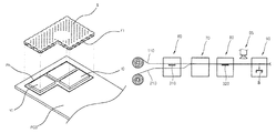
- a shield can S may include a lid L and a frame F assembled to the inside of the lid L.
- the lid L and the frame F are separately formed by press and then manually assembled or input to a separate assembly device to be assembled in one body. Accordingly, productivity is low compared to high manufacturing costs.
- Korean Patent No. 10-0456126 discloses an apparatus that includes a material supply portion 100 , a sensing guide portion 200 , an assembly portion 300 , a transfer portion 400 , a scrap cutting portion 1 500 , a finished product cutting portion 600 , and a scrap cutting portion 2 700 , thereby enabling automation of a manufacturing process of the shield can S.
- the lid L having a certain shape and a downwardly bent edge, and the frame adequately inserted into the inside of the lid L and having a contact portion F 1 provided along the edge.
- a first-tier flat band 10 on which the lids L are continuously and repeatedly press-formed in a lengthwise direction thereof, is supplied in an upper side, and simultaneously, a second-tier flat band 20 , on which the frames F are continuously and repeatedly press-formed in the lengthwise direction thereof, is supplied in a lower side.
- the frame F is punched to be inserted into the lid L formed on the first-tier flat band 10 while cutting support ends 21 of the frame F formed on the second-tier flat band 20 .
- support ends 11 of the lid L formed on the first-tier flat band 10 are cut so that the shield can S may be finished.
- the above apparatus and method of manufacturing a shield for IC device has a merit of enabling automation of a shield can manufacturing process and thus reducing a defect rate.
- the present inventive concept provides a method of manufacturing a shield can for blocking electromagnetic waves, by which the electromagnetic waves may be efficiently blocked, compared to a related art.
- the present inventive concept provides a method of manufacturing a shield can for blocking electromagnetic waves, by which lowering of an adhesion force of a shielding tape and contamination of an electronic device adopting a shield can may be prevented.
- the present inventive concept provides a method of manufacturing a shield can for blocking electromagnetic waves, which facilitates collection of a used shielding tape that is punched.
- a method of manufacturing a shield can for blocking electromagnetic waves including a lid and a frame assembled to each other, the method including supplying a first metal band for manufacturing the lid by intermittently drawing the first metal band from a bobbin around which the first metal band is wound in a roll shape, and supplying a second metal band for manufacturing the frame by intermittently drawing the second metal band from a bobbin around which the second metal band is wound in a roll shape, pressing each of the first and second metal bands thus supplied so that the lid and the frame are continuously formed on the first and second metal bands and remain on the first and second metal bands by connection bands, cleaning and drying the first and second metal bands thus pressed, intermittently supplying the first metal band thus cleaned in an upper side, and intermittently supplying the second metal band in a lower side of the first metal band, in parallel to each other, attaching a first shielding tape to a lower surface of the lid on the first metal band, assembling the lid and the frame by cutting the connection bands of
- the first and second metal bands may be ultrasound-cleaned by passing through a cleaning reservoir where a cleaning water is filled and ultrasound waves are generated by an ultrasound generator, and the cleaning water remaining on the first and second metal bands may be removed by blowing air
- the first shielding tape may include a shielding tape having one surface coated with an adhesive and a transfer sheet detachably attached to the adhesive of the shielding tape, the first shielding tape may be supplied with the shielding tape and the transfer sheet being separated from the first shielding tape, the shielding tape thus separated may be punched and the shielding tape thus punched may be attached to the lower surface of the lid, and the shielding tape that remains after being punched and the transfer sheet may be reattached to each other and discharged.
- first and second metal bands 110 and 210 are ultrasound-cleaned so that a contaminant such as oil and moisture on the surfaces thereof are removed. Accordingly, the lowering of an adhesion force of a shielding tape may be prevented and an electronic device adopting a shield can S may be prevented from being contaminated.
- the shielding tape is attached to a lid L and a frame F, electromagnetic waves may be efficiently blocked and an assembly process of the lid L and the frame F and an attachment process of the shielding tape may be automated.
- a shielding tape 311 that remains after being punched and a transfer sheet 312 are reattached to each other and discharged. Accordingly, a separate collecting roller is not necessary, and further, even when a first shielding tape 310 that is collected is accommodated in a collection container, the first shielding tape 310 may be easily collected from the collection container because adhesiveness of an adhesive 313 does not work.
- FIGS. 1 and 2 schematically illustrate a structure of a typical shield can.
- FIGS. 3 and 4 schematically illustrate a method of manufacturing a shield can according to a related art.
- FIG. 5 is an image of a shield can in a disassembled state that is manufactured by a manufacturing method according to an embodiment.
- FIG. 6 is an image of the shield can of FIG. 5 in an assembled state.
- FIG. 7 is an image of a first metal band pressed in a lid shape.
- FIG. 8 is an image of a second metal band pressed in a frame shape.
- FIGS. 9 and 10 schematically illustrate process of a manufacturing method according to an embodiment.
- FIG. 11 illustrates a cleaning process
- FIG. 12 illustrates a first shielding tape attachment process
- FIG. 13 is a perspective view of a first shielding tape.
- a method of manufacturing a shield can may efficiently block electromagnetic waves compared to a related art, prevent lowering of an adhesion force of a shielding tape to a lid and a frame, and prevent contamination of an electronic device adopting the shield can.
- a shield can S has a structure in which a lid L and a frame F are assembled to each other and shielding tapes 311 and 321 are respectively attached to the lid L and the frame F.
- the shield can S is automatically assembled as a first metal band 110 continuously pressed in a shape of the lid L and a second metal band 210 continuously pressed in a shape of the frame F are respectively supplied in upper and lower sides and a first shielding tape 310 is supplied on a supply path of the first and second metal bands 110 and 210 .
- the shield can S as above may surround the exterior of an electronic part and absorb or block electromagnetic waves emitted from the electronic part.
- a method of manufacturing a shield can according to an embodiment is described as follows.
- the first metal band 110 for manufacturing the lid L is supplied by being intermittently drawn from a bobbin 101 around which the first metal band 110 is rolled in a roll shape.
- the second metal band 210 for manufacturing the frame F is supplied by being intermittently drawn from a bobbin 201 around which the second metal band 210 is rolled in a roll shape.
- An apparatus used for the process of FIG. 9 is manufactured in a pair so that the first metal band 110 and the second metal band 210 may be simultaneously supplied.
- the first metal band 110 and the second metal band 210 released from the bobbin 101 ( 201 ) are planarized through a leveling process 30 .
- first metal band 110 and the second metal band 210 that are thin metal films may be deformed; for example, the first and second metal bands 110 and 210 may be bent during transfer. Accordingly, the first metal band 110 and the second metal band 210 may be planarized through the leveling process 30 .
- the first metal band 110 and the second metal band 210 are planarized by passing between a plurality of rollers arranged up and down and zigzag.
- Each of the first metal band 110 and the second metal band 210 that are planarized may be step-transferred by a feeder 35 and supplied to a pressing process 40 .
- the shapes of the lid L and the frame F are continuously formed on the first and second metal bands 110 and 210 and thus the lid L and the frame F respectively remain on the first and second metal bands 110 and 210 by connection bands 111 and 211 .
- the first and second metal bands 110 and 210 that are pressed are cleaned and dried through a cleaning process 50 .
- the first and second metal bands 110 and 210 that are pressed are ultrasound-cleaned by passing through a cleaning reservoir where cleaning water 52 is filled and ultrasound waves are generated by an ultrasound generator 51 .
- the cleaning water 52 remaining on the first and second metal bands 110 and 210 are removed by blowing high pressure air through pipes 53 and 54 .
- the first and second metal bands 110 and 210 that are cleaned are rolled in a roll shape as illustrated in the rightmost side of FIG. 9 .
- the first and second metal bands 110 and 210 that are rolled in a roll shape as above are arranged in upper and lower sides as illustrated in FIG. 10 , and the first metal band 110 is intermittently supplied in the upper side and the second metal band 210 is intermittently supplied in the lower side of the first metal band 110 , in parallel to each other.
- the first shielding tape 310 is attached to a lower surface of the lid L on the first metal band 110
- the first shielding tape 310 may include the shielding tape 311 having one surface coated with an adhesive 313 and a transfer sheet 312 detachably attached to the adhesive 313 of the shielding tape 311 .
- the first shielding tape 310 is supplied in a perpendicular direction to a direction in which the first metal band 110 is supplied, and the first and second metal bands 110 and 210 are transferred by being arranged in upper and lower sides of a guide block 61 .
- the first shielding tape 310 that is released from a tape roll 301 by a rotational driving force of a drawing roller 65 is supplied by being separated into the shielding tape 311 and the transfer sheet 312 .
- the shielding tape 311 that is separated is punched and then the shielding tape 311 that is punched is attached to the lower surface of the lid L of the first metal band 110 .
- the shielding tape 311 that remains after being punched and the transfer sheet 312 are reattached to each other and discharged.
- the shielding tape 311 that remains after being punched and the transfer sheet 312 are reattached to each other and discharged, a separate collecting roller is not necessary and, even when the first shielding tape 310 that is collected is accommodated in an collection container 69 , the adhesiveness of the adhesive 313 does not work so that the first shielding tape 310 may be easily collected from the collection container 69 .
- the lid L and the frame F are assembled to each other while cutting the connection bands 111 and 211 of the lid L to which the first shielding tape 310 is attached and the frame F to which the shielding tape 310 is not attached (a cutting and assembly process 70 of FIG. 10 )
- the lid L and the frame F that are assembled to each other are transferred together on the same plane as the first and second metal bands 110 and 210 .
- a camera vision test may be performed to check an assembly error.
- a second shielding tape 320 is attached to a lower surface of the frame F that is assembled to the lid L.
- the shield can S that is manufactured is transferred to a package process, and the first and second metal bands 110 and 210 are destroyed at a certain interval and discharged.
- the shield can S that is manufactured undergoes a shielding tape attachment state test and then is packaged.
- the first and second metal bands 110 and 210 are ultrasound-cleaned to remove contaminants such as oil on the surfaces thereof, lowering of adhesiveness of the shielding tape may be prevented and an electronic product adopting the shield can S may be prevented from being contaminated.
- the shielding tape is attached on the lid L and the frame F, electromagnetic waves may be efficiently blocked, and the assembly process of the lid L and the frame F and the attachment process of the shielding tape may be automated.
- the method of manufacturing a shield can for blocking electromagnetic waves relates to a method of manufacturing a shield can which absorbs and blocks electromagnetic waves generated in a circuit device inside an electronic device such as a portable phone, a PCS, or an RF communication apparatus, by which a manufacturing process of from forming a lid and a frame from metal bands wound around a supply roll to attaching a shielding tape to a shield can may be continuously performed.
Landscapes
- Engineering & Computer Science (AREA)
- Microelectronics & Electronic Packaging (AREA)
- Physics & Mathematics (AREA)
- Electromagnetism (AREA)
- Shielding Devices Or Components To Electric Or Magnetic Fields (AREA)
- Health & Medical Sciences (AREA)
- Toxicology (AREA)
- Details Of Aerials (AREA)
Abstract
Description
Claims (4)
Applications Claiming Priority (3)
| Application Number | Priority Date | Filing Date | Title |
|---|---|---|---|
| KR10-2014-0017828 | 2014-02-17 | ||
| KR1020140017828A KR101425179B1 (en) | 2014-02-17 | 2014-02-17 | Method for manufacturing shield can for electromagnetic shielding |
| PCT/KR2015/001600 WO2015122745A1 (en) | 2014-02-17 | 2015-02-17 | Method for manufacturing shield can for blocking electromagnetic wave |
Publications (2)
| Publication Number | Publication Date |
|---|---|
| US20170013749A1 US20170013749A1 (en) | 2017-01-12 |
| US10194567B2 true US10194567B2 (en) | 2019-01-29 |
Family
ID=51749146
Family Applications (1)
| Application Number | Title | Priority Date | Filing Date |
|---|---|---|---|
| US15/119,656 Expired - Fee Related US10194567B2 (en) | 2014-02-17 | 2015-02-17 | Method for manufacturing shield cans for blocking electromagnetic waves |
Country Status (4)
| Country | Link |
|---|---|
| US (1) | US10194567B2 (en) |
| KR (1) | KR101425179B1 (en) |
| CN (1) | CN106465567B (en) |
| WO (1) | WO2015122745A1 (en) |
Families Citing this family (8)
| Publication number | Priority date | Publication date | Assignee | Title |
|---|---|---|---|---|
| KR101477979B1 (en) * | 2014-02-17 | 2015-01-02 | 주식회사 라프리마 | Apparatus for feeding a shield tape for electromagnetic shielding |
| FI127786B (en) * | 2015-07-20 | 2019-02-28 | Prism Microwave Oy | Process for producing a component of an RF filter, a component and an RF filter |
| KR20170012960A (en) | 2015-07-27 | 2017-02-06 | 삼성전자주식회사 | Electromagnetic wave shield thin film and method of forming the same |
| KR101699360B1 (en) * | 2015-10-29 | 2017-01-24 | 주식회사 에이엠텍 | device and method to attach insulation tape to shield can for camera module |
| KR101822049B1 (en) * | 2016-06-28 | 2018-03-08 | 삼육구 주식회사 | Apparatus for manufacturing shield can for electromagnetic shielding |
| KR102544367B1 (en) | 2016-11-08 | 2023-06-19 | 삼성전자주식회사 | Electronic device with electromagnetic shielding member |
| KR101798028B1 (en) | 2017-08-03 | 2017-11-16 | 주식회사 유경하이테크 | shield can manufacturing apparatus for electromagnetic shielding |
| KR102081995B1 (en) * | 2018-02-07 | 2020-02-26 | 주재철 | Apparatus for vision inspecting and packing shielded cans |
Citations (4)
| Publication number | Priority date | Publication date | Assignee | Title |
|---|---|---|---|---|
| KR100456126B1 (en) | 2002-12-18 | 2004-11-08 | 정태열 | Shield assembling system ans method |
| KR100673531B1 (en) | 2005-01-31 | 2007-01-24 | 주식회사 에이엠아이 씨 | Thin electromagnetic shielding tape, electromagnetic shielding structure using the same and manufacturing method thereof |
| KR100729708B1 (en) | 2005-09-26 | 2007-06-19 | 주식회사 케이와이에스 | Method for manufacturing shield can of mobile phone terminal by pressing process |
| KR101217708B1 (en) | 2012-09-05 | 2013-01-02 | 주식회사 케이텍 | Method for manufacturing shield can which uses metal board by supplying roll and shield can manufactured with this |
Family Cites Families (5)
| Publication number | Priority date | Publication date | Assignee | Title |
|---|---|---|---|---|
| DE3634367A1 (en) * | 1986-10-09 | 1988-04-21 | Schloemann Siemag Ag | ROLLER ARRANGEMENT FOR DEFORM-FREE TREATMENT OF MOVING TAPE-SHAPED PRODUCTS |
| IT1305116B1 (en) * | 1998-09-14 | 2001-04-10 | Zincocelere Spa | COMPONENT FOR MULTILAYER PRINTED CIRCUIT, METHOD FOR SUABABRICATION AND RELATED MULTI-PURPOSE PRINTED CIRCUIT. |
| CN100498828C (en) * | 2004-04-27 | 2009-06-10 | 大日本印刷株式会社 | Method for manufacturing sheet provided with IC tag, apparatus for manufacturing sheet provided with IC tag and IC tag |
| KR101352944B1 (en) | 2007-08-16 | 2014-01-22 | 김동현 | EMI Shielding Material and Method of manufacturing |
| KR101095489B1 (en) | 2011-04-13 | 2011-12-16 | (주)한비메탈텍 | Shield can plate material for SMD process, manufacturing method thereof and shield can using the plate material |
-
2014
- 2014-02-17 KR KR1020140017828A patent/KR101425179B1/en active Active
-
2015
- 2015-02-17 US US15/119,656 patent/US10194567B2/en not_active Expired - Fee Related
- 2015-02-17 CN CN201580020137.6A patent/CN106465567B/en not_active Expired - Fee Related
- 2015-02-17 WO PCT/KR2015/001600 patent/WO2015122745A1/en not_active Ceased
Patent Citations (4)
| Publication number | Priority date | Publication date | Assignee | Title |
|---|---|---|---|---|
| KR100456126B1 (en) | 2002-12-18 | 2004-11-08 | 정태열 | Shield assembling system ans method |
| KR100673531B1 (en) | 2005-01-31 | 2007-01-24 | 주식회사 에이엠아이 씨 | Thin electromagnetic shielding tape, electromagnetic shielding structure using the same and manufacturing method thereof |
| KR100729708B1 (en) | 2005-09-26 | 2007-06-19 | 주식회사 케이와이에스 | Method for manufacturing shield can of mobile phone terminal by pressing process |
| KR101217708B1 (en) | 2012-09-05 | 2013-01-02 | 주식회사 케이텍 | Method for manufacturing shield can which uses metal board by supplying roll and shield can manufactured with this |
Also Published As
| Publication number | Publication date |
|---|---|
| WO2015122745A1 (en) | 2015-08-20 |
| CN106465567A (en) | 2017-02-22 |
| KR101425179B1 (en) | 2014-08-01 |
| US20170013749A1 (en) | 2017-01-12 |
| CN106465567B (en) | 2019-07-05 |
Similar Documents
| Publication | Publication Date | Title |
|---|---|---|
| US10194567B2 (en) | Method for manufacturing shield cans for blocking electromagnetic waves | |
| CN114139668A (en) | Antenna pattern, RFID inlet, RFID tag, and method for manufacturing RFID medium | |
| CN104037444B (en) | Side band attachment arrangement for plain battery | |
| CN113473715B (en) | Laser cutting and laminating method and device for FPC (flexible printed circuit) board | |
| CN103179790A (en) | Hybrid printed circuit board and manufacturing method thereof | |
| KR101051857B1 (en) | How to attach the member plate to the FPC product | |
| KR101590428B1 (en) | Method for manufacturing thin type of antenna | |
| JP2013227065A (en) | Carrier tape for holding electronic component, and manufacturing method and package of carrier tape for holding electronic component | |
| JP5702110B2 (en) | Electronic component mounting apparatus and mounting method | |
| KR101477979B1 (en) | Apparatus for feeding a shield tape for electromagnetic shielding | |
| KR101407535B1 (en) | Tape attaching apparatus for pcb | |
| KR101666441B1 (en) | Edge Coating Apparatus of Metal Copper Clad Laminate | |
| KR101822049B1 (en) | Apparatus for manufacturing shield can for electromagnetic shielding | |
| KR101122721B1 (en) | Electric conductive gasket and method for manufacturing the same | |
| KR101746289B1 (en) | Shield can having inside and outside isolation film and manufacture method thereof | |
| CN103451655B (en) | With film etch process and application and with the obtained Metal Flake component of its processing | |
| KR102513880B1 (en) | Roll packing method of electromagnetic shielding gasket | |
| KR102127207B1 (en) | A flexible coil and a method for manufacturing the same | |
| CN104386286A (en) | Forming process of metal strap of film sticking frame type part | |
| KR101412240B1 (en) | laminating method of partially insulating layer on the metal sheet for shield can and device thereof | |
| KR20180116611A (en) | Method for manufacturing shield for shielding electromagnetic wave | |
| CN110586428A (en) | Processing technology of insulation shielding case | |
| CN108668464A (en) | A kind of method and article construction of ultra-thin soft board and metal terminal ultrasonic bonding | |
| CN117979220A (en) | Method for assembling pickup MIC and terminal equipment | |
| TWI523595B (en) | Smart card chip continuous strip carrier board and the use of long strip and forming method |
Legal Events
| Date | Code | Title | Description |
|---|---|---|---|
| AS | Assignment |
Owner name: LAPRIMA CO., LTD., KOREA, REPUBLIC OF Free format text: ASSIGNMENT OF ASSIGNORS INTEREST;ASSIGNORS:NAM, KYUNG SIK;AHN, KEUN HUN;REEL/FRAME:039717/0694 Effective date: 20160816 |
|
| AS | Assignment |
Owner name: 369 TECH CO., LTD., KOREA, REPUBLIC OF Free format text: ASSIGNMENT OF ASSIGNORS INTEREST;ASSIGNOR:LAPRIMA CO., LTD.;REEL/FRAME:039765/0634 Effective date: 20160819 |
|
| STCF | Information on status: patent grant |
Free format text: PATENTED CASE |
|
| FEPP | Fee payment procedure |
Free format text: MAINTENANCE FEE REMINDER MAILED (ORIGINAL EVENT CODE: REM.); ENTITY STATUS OF PATENT OWNER: SMALL ENTITY |
|
| LAPS | Lapse for failure to pay maintenance fees |
Free format text: PATENT EXPIRED FOR FAILURE TO PAY MAINTENANCE FEES (ORIGINAL EVENT CODE: EXP.); ENTITY STATUS OF PATENT OWNER: SMALL ENTITY |
|
| STCH | Information on status: patent discontinuation |
Free format text: PATENT EXPIRED DUE TO NONPAYMENT OF MAINTENANCE FEES UNDER 37 CFR 1.362 |
|
| FP | Lapsed due to failure to pay maintenance fee |
Effective date: 20230129 |