US10176930B2 - Low profile flat wet electrolytic tantalum capacitor - Google Patents
Low profile flat wet electrolytic tantalum capacitor Download PDFInfo
- Publication number
- US10176930B2 US10176930B2 US14/995,909 US201614995909A US10176930B2 US 10176930 B2 US10176930 B2 US 10176930B2 US 201614995909 A US201614995909 A US 201614995909A US 10176930 B2 US10176930 B2 US 10176930B2
- Authority
- US
- United States
- Prior art keywords
- outer case
- low profile
- wet electrolytic
- capacitor
- electrolytic capacitor
- Prior art date
- Legal status (The legal status is an assumption and is not a legal conclusion. Google has not performed a legal analysis and makes no representation as to the accuracy of the status listed.)
- Active, expires
Links
- 239000003990 capacitor Substances 0.000 title claims abstract description 175
- GUVRBAGPIYLISA-UHFFFAOYSA-N tantalum atom Chemical compound [Ta] GUVRBAGPIYLISA-UHFFFAOYSA-N 0.000 title claims description 30
- 229910052715 tantalum Inorganic materials 0.000 title claims description 28
- 239000003792 electrolyte Substances 0.000 claims abstract description 10
- 238000004891 communication Methods 0.000 claims abstract description 9
- 239000012530 fluid Substances 0.000 claims abstract description 9
- WABPQHHGFIMREM-UHFFFAOYSA-N lead(0) Chemical compound [Pb] WABPQHHGFIMREM-UHFFFAOYSA-N 0.000 claims description 31
- 239000012212 insulator Substances 0.000 claims description 26
- 229910052751 metal Inorganic materials 0.000 claims description 18
- 239000002184 metal Substances 0.000 claims description 18
- 230000015572 biosynthetic process Effects 0.000 claims description 11
- 238000000034 method Methods 0.000 abstract description 7
- 230000000712 assembly Effects 0.000 abstract 1
- 238000000429 assembly Methods 0.000 abstract 1
- 239000000463 material Substances 0.000 description 16
- PXHVJJICTQNCMI-UHFFFAOYSA-N Nickel Chemical compound [Ni] PXHVJJICTQNCMI-UHFFFAOYSA-N 0.000 description 12
- 229920001343 polytetrafluoroethylene Polymers 0.000 description 9
- 239000004810 polytetrafluoroethylene Substances 0.000 description 9
- 230000007613 environmental effect Effects 0.000 description 7
- 238000010586 diagram Methods 0.000 description 6
- 230000008569 process Effects 0.000 description 6
- 238000004519 manufacturing process Methods 0.000 description 5
- 229910052759 nickel Inorganic materials 0.000 description 5
- BPUBBGLMJRNUCC-UHFFFAOYSA-N oxygen(2-);tantalum(5+) Chemical compound [O-2].[O-2].[O-2].[O-2].[O-2].[Ta+5].[Ta+5] BPUBBGLMJRNUCC-UHFFFAOYSA-N 0.000 description 5
- PBCFLUZVCVVTBY-UHFFFAOYSA-N tantalum pentoxide Inorganic materials O=[Ta](=O)O[Ta](=O)=O PBCFLUZVCVVTBY-UHFFFAOYSA-N 0.000 description 5
- BFRGSJVXBIWTCF-UHFFFAOYSA-N niobium monoxide Chemical compound [Nb]=O BFRGSJVXBIWTCF-UHFFFAOYSA-N 0.000 description 4
- 239000012811 non-conductive material Substances 0.000 description 4
- 239000008188 pellet Substances 0.000 description 4
- -1 polytetrafluoroethylene Polymers 0.000 description 4
- 238000003466 welding Methods 0.000 description 4
- KDLHZDBZIXYQEI-UHFFFAOYSA-N Palladium Chemical compound [Pd] KDLHZDBZIXYQEI-UHFFFAOYSA-N 0.000 description 3
- 239000010955 niobium Substances 0.000 description 3
- 229910000990 Ni alloy Inorganic materials 0.000 description 2
- 239000004809 Teflon Substances 0.000 description 2
- 229920006362 Teflon® Polymers 0.000 description 2
- 239000010405 anode material Substances 0.000 description 2
- 230000004888 barrier function Effects 0.000 description 2
- 229910052758 niobium Inorganic materials 0.000 description 2
- GUCVJGMIXFAOAE-UHFFFAOYSA-N niobium atom Chemical compound [Nb] GUCVJGMIXFAOAE-UHFFFAOYSA-N 0.000 description 2
- 230000003647 oxidation Effects 0.000 description 2
- 238000007254 oxidation reaction Methods 0.000 description 2
- 229920003223 poly(pyromellitimide-1,4-diphenyl ether) Polymers 0.000 description 2
- 230000035939 shock Effects 0.000 description 2
- RTAQQCXQSZGOHL-UHFFFAOYSA-N Titanium Chemical compound [Ti] RTAQQCXQSZGOHL-UHFFFAOYSA-N 0.000 description 1
- 229910045601 alloy Inorganic materials 0.000 description 1
- 239000000956 alloy Substances 0.000 description 1
- 239000011248 coating agent Substances 0.000 description 1
- 238000000576 coating method Methods 0.000 description 1
- 238000010276 construction Methods 0.000 description 1
- 230000001934 delay Effects 0.000 description 1
- 239000003989 dielectric material Substances 0.000 description 1
- 230000005611 electricity Effects 0.000 description 1
- 239000011521 glass Substances 0.000 description 1
- 230000008676 import Effects 0.000 description 1
- 239000011810 insulating material Substances 0.000 description 1
- 238000002955 isolation Methods 0.000 description 1
- WABPQHHGFIMREM-NOHWODKXSA-N lead-200 Chemical compound [200Pb] WABPQHHGFIMREM-NOHWODKXSA-N 0.000 description 1
- 238000012423 maintenance Methods 0.000 description 1
- 229910052763 palladium Inorganic materials 0.000 description 1
- 238000003825 pressing Methods 0.000 description 1
- 230000009467 reduction Effects 0.000 description 1
- 230000008439 repair process Effects 0.000 description 1
- 238000007789 sealing Methods 0.000 description 1
- 239000007787 solid Substances 0.000 description 1
- 230000008961 swelling Effects 0.000 description 1
- 229910052719 titanium Inorganic materials 0.000 description 1
- 239000010936 titanium Substances 0.000 description 1
Images


Classifications
-
- H—ELECTRICITY
- H01—ELECTRIC ELEMENTS
- H01G—CAPACITORS; CAPACITORS, RECTIFIERS, DETECTORS, SWITCHING DEVICES, LIGHT-SENSITIVE OR TEMPERATURE-SENSITIVE DEVICES OF THE ELECTROLYTIC TYPE
- H01G9/00—Electrolytic capacitors, rectifiers, detectors, switching devices, light-sensitive or temperature-sensitive devices; Processes of their manufacture
- H01G9/004—Details
- H01G9/08—Housing; Encapsulation
- H01G9/10—Sealing, e.g. of lead-in wires
-
- H—ELECTRICITY
- H01—ELECTRIC ELEMENTS
- H01G—CAPACITORS; CAPACITORS, RECTIFIERS, DETECTORS, SWITCHING DEVICES, LIGHT-SENSITIVE OR TEMPERATURE-SENSITIVE DEVICES OF THE ELECTROLYTIC TYPE
- H01G9/00—Electrolytic capacitors, rectifiers, detectors, switching devices, light-sensitive or temperature-sensitive devices; Processes of their manufacture
- H01G9/0029—Processes of manufacture
-
- H—ELECTRICITY
- H01—ELECTRIC ELEMENTS
- H01G—CAPACITORS; CAPACITORS, RECTIFIERS, DETECTORS, SWITCHING DEVICES, LIGHT-SENSITIVE OR TEMPERATURE-SENSITIVE DEVICES OF THE ELECTROLYTIC TYPE
- H01G9/00—Electrolytic capacitors, rectifiers, detectors, switching devices, light-sensitive or temperature-sensitive devices; Processes of their manufacture
- H01G9/004—Details
- H01G9/02—Diaphragms; Separators
-
- H—ELECTRICITY
- H01—ELECTRIC ELEMENTS
- H01G—CAPACITORS; CAPACITORS, RECTIFIERS, DETECTORS, SWITCHING DEVICES, LIGHT-SENSITIVE OR TEMPERATURE-SENSITIVE DEVICES OF THE ELECTROLYTIC TYPE
- H01G9/00—Electrolytic capacitors, rectifiers, detectors, switching devices, light-sensitive or temperature-sensitive devices; Processes of their manufacture
- H01G9/004—Details
- H01G9/022—Electrolytes; Absorbents
- H01G9/035—Liquid electrolytes, e.g. impregnating materials
-
- H—ELECTRICITY
- H01—ELECTRIC ELEMENTS
- H01G—CAPACITORS; CAPACITORS, RECTIFIERS, DETECTORS, SWITCHING DEVICES, LIGHT-SENSITIVE OR TEMPERATURE-SENSITIVE DEVICES OF THE ELECTROLYTIC TYPE
- H01G9/00—Electrolytic capacitors, rectifiers, detectors, switching devices, light-sensitive or temperature-sensitive devices; Processes of their manufacture
- H01G9/145—Liquid electrolytic capacitors
-
- H—ELECTRICITY
- H01—ELECTRIC ELEMENTS
- H01G—CAPACITORS; CAPACITORS, RECTIFIERS, DETECTORS, SWITCHING DEVICES, LIGHT-SENSITIVE OR TEMPERATURE-SENSITIVE DEVICES OF THE ELECTROLYTIC TYPE
- H01G9/00—Electrolytic capacitors, rectifiers, detectors, switching devices, light-sensitive or temperature-sensitive devices; Processes of their manufacture
- H01G9/26—Structural combinations of electrolytic capacitors, rectifiers, detectors, switching devices, light-sensitive or temperature-sensitive devices with each other
Definitions
- This application relates to the field of electronic components, and more specifically, capacitors.
- wet capacitors are used in the design of circuits due to their volumetric efficiency, stable electrical parameters, high reliability and long service life. Such capacitors typically have a larger capacitance per unit volume than certain other types of capacitors, making them valuable in high-current, high-power, and low-frequency electrical circuits.
- One type of wet capacitor is a wet electrolytic capacitor.
- a wet electrolytic capacitor includes two conducting surfaces (an anode and a cathode) whose function is to conduct electricity, and a fluid electrolyte. An insulating material or dielectric separates the two conducting surfaces. Wet electrolytic capacitors tend to offer a good combination of high capacitance and low leakage current.
- wet electrolytic capacitors are basic to various types of electrical equipment from satellites, aerospace, airborne, military group support, oil exploration, power supplies, and the like.
- the capacitor may be exposed to harsh environmental conditions, including extreme temperatures, pressure, moisture, shock, vibration, and the like.
- the capacitor must be able to withstand these harsh environmental conditions while maintaining its accuracy, service life, and ability to be powered at very high temperatures with no maintenance. Failure of a capacitor due to harsh environmental conditions would necessitate its removal for repairs, which would result in delays and other associated expenses.
- many of these example applications include significant dimensional or layout constraints, as the field of electronics is consistently demanding smaller parts and devices. For example, reductions in both mounting area and component profile (i.e., height) are highly demanded in most current applications.
- Tantalum electrolytic capacitors such as Tantalum (Ta) electrolytic capacitors
- Tantalum electrolytic capacitors known in the art may use tantalum for the anode material.
- the tantalum anode body also commonly referred to as a “slug” or “pellet”
- a wire (which may also be formed of tantalum) is commonly formed in the anode body in one of two ways: (1) “embedded,” meaning the wire is covered with tantalum powder during a pressing process; or (2) “welded,” meaning after the pellet is pressed and sintered, the wire is welded to the tantalum anode body.
- the other end of the wire extends outside of the tantalum anode body.
- the capacitor dielectric material may be made by anodic oxidation of the anode material to form an oxide layer over the surface of the anode body (e.g., Ta to Ta 2 O 5 ).
- a capacitor cathode may be formed by coating an inner surface of the body or case of the capacitor that encloses the tantalum anode body.
- the cathode may be formed of sinter tantalum or electrophoretically deposited tantalum, and may be attached to a cathode wire.
- a fluid electrolyte separates the cathode and the anode body and provides for electrical communication between the cathode and anode body.
- cylindrical shaped capacitors with axial leaded terminations generally perform reliably in harsh environmental conditions, their provided energy density is limited by their cylindrical shape and limited surface area of their conducting surfaces (anode and cathode), as the surface area of the two conducting surfaces determines the capacitance of the capacitor. Additionally, dimensional constraints often make their application difficult.
- circular or square shaped capacitor body or “can” with radial leaded terminations Other types of known wet electrolytic capacitors are characterized as having a circular or square shaped capacitor body or “can” with radial leaded terminations. While circular or square shaped capacitors with radial leaded terminations may provide higher energy density when compared to cylindrical shaped capacitors with axial leaded terminations, their ability to operate in harsh environmental conditions is limited. For example, circular or square shaped capacitors with radial leaded terminations generally are more susceptible to elevated temperatures that cause capacitor swelling. Additionally, circular or square shaped capacitors with radial leaded terminations generally have limited ability to survive in high shock or vibration environments.
- a low profile wet electrolytic capacitor in one aspect of the present invention, includes an outer case assembly.
- the outer case assembly is formed by an outer case and outer case cover that is hermetically sealed to the outer case.
- the outer case assembly includes an interior area.
- a capacitive element is positioned in the interior area.
- the capacitive element is isolated from the outer case assembly by one or more insulative elements.
- a connecting tube is positioned perpendicular to and attached to the outer case and the outer case cover and passes through an opening in the capacitive element.
- An isolated positive lead is positioned on the outer case assembly and is in electrical communication with the capacitive element.
- a negative terminal is positioned on the outer case assembly.
- a fluid electrolyte is contained in the interior area of the outer case assembly.
- the present invention is also directed to, in another aspect, multiple low profile wet electrolytic capacitors mounted in a capacitor stack.
- Multiple low profile wet electrolytic capacitors may be mounted in a stacked formation or capacitor stack and electrically connected to one another in parallel or in series.
- a method of making a low profile wet electrolytic capacitor may preferably comprise the steps of: forming an outer case defining an interior area; forming an outer case opening in a wall of the outer case; positioning an insulator band around a perimeter of the interior area of the outer case; forming a connecting tube; welding the connecting tube to the outer case at the outer case opening; positioning an insulator tube over the connecting tube; forming an outer case cover; forming an outer case cover opening in a wall of the outer case cover; positioning a first and second cathode layer on an internal surface of the outer case and the outer case cover; forming a capacitor element; positioning the capacitive element in the interior area of the outer case; welding the outer case cover to the outer case and connecting tube; positioning a positive lead insulator over the outer case; welding a positive lead over the positive lead insulator to the cathode element; and welding a negative terminal to the outer case.
- a method of making a low profile wet electrolytic capacitor stack assembly having a plurality of capacitors electrically connected to one other in parallel or in series is also provided.
- FIG. 1 is an isometric view of a capacitor according to an embodiment of the present invention
- FIG. 1A is an enlarged detailed view of the area defined by 1 A in FIG. 1 ;
- FIG. 2 is a left side view of a capacitor according to an embodiment of the present invention.
- FIG. 3 is a cross-sectional view from the top of the capacitor according to an embodiment of the present invention taken along line 3 - 3 of FIG. 2 ;
- FIG. 3A is an enlarged detailed view of the area defined by 3 A in FIG. 3 ;
- FIG. 4 is a cross-sectional view from the bottom of the capacitor according to an embodiment of the present invention taken along line 4 - 4 of FIG. 2 ;
- FIG. 4A is an enlarged detailed view of the area defined by 4 A in FIG. 4 ;
- FIG. 5 is an exploded view of a capacitor case and case wall assembly according to an embodiment of the present invention.
- FIG. 6 is an exploded view of an anode assembly according to an embodiment of the present invention.
- FIG. 7 is an isometric view of several capacitors mounted in a stacked formation and connected in parallel according to an embodiment of the present invention.
- FIG. 8A is an isometric view of several capacitors mounted in a stacked formation and connected in series according to an embodiment of the present invention
- FIG. 8B is an isometric view of several capacitors mounted in a stacked formation and connected in series according to an embodiment of the present invention.
- FIG. 9 is a flow diagram of a process for assembling a capacitor according to an embodiment of the present invention.
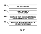
- FIG. 10 is a flow diagram of a process for making the capacitor element according to an embodiment of the present invention.
- FIG. 11 is a flow diagram of a process for assembling a capacitor according to an embodiment of the present invention.
- FIG. 12 is a flow diagram of a process for assembling a stacked capacitor assembly connected in parallel according to an embodiment of the present invention.
- FIG. 13 is a flow diagram of a process for assembling a stacked capacitor assembly connected in series according to an embodiment of the present invention.
- FIGS. 1-6 show a capacitor 100 according to an embodiment of the present invention.
- the capacitor 100 includes an outer case assembly 105 comprising an outer case 102 and outer case cover 104 .
- the outer case 102 may be formed of metal, such as tantalum (Ta) and forms part of the cathode of the capacitor 100 .
- the outer case 102 has a front side 106 , a rear side 108 , a left side 110 , a right side 112 , and a top 114 .
- the outer case 102 preferably has an open end as shown in FIG. 5 .
- the outer case cover 104 may be formed of the same metal as the outer case 102 (i.e., tantalum if tantalum is also used as the material of the outer case 102 ), and may be hermetically welded to the open end of the outer case 102 as shown in FIG. 5 .
- the outer case cover 104 also forms part of the cathode. While the shape of the outer case 102 may vary, in an embodiment of the present invention and as shown in FIGS. 1-4 , the sides 106 , 108 , 110 , 112 may have a generally rectangular shape, and the top 114 may have a generally square overall shape.
- the outer case assembly 105 is formed.
- the outer case 102 further comprises an outer case opening 103 which may preferably be formed centrally in the top 114 of the outer case 102 .
- the outer case cover 104 further comprises an outer case cover opening 107 which may preferably be formed centrally in the outer case cover 104 , and is sized and positioned to align with the outer case opening 103 .
- the outer case 102 further comprises an anode termination opening 111 .
- the outer case assembly 105 has a length L, a width W, and a height H. As shown in FIGS. 1, 2, and 5 , the outer case assembly 105 forms a generally flat rectangular or square cuboid or prism with an interior area 109 or cavity. The sides 106 - 112 and top 114 of the outer case 102 may also have rounded or beveled edges at the corners 116 .
- the ratio of width W to height H of the outer case assembly 105 should preferably be at least 4:1 to provide a low profile and to allow for the greatest amount of surface area of the conducing surfaces (i.e., anode and cathode). However, varying ratios, that are greater or less than 4:1, may be used to comply with dimensional constraints.
- the shape and construction of the outer case 102 assists in providing improved energy density over known capacitors while also providing a reduced height or profile that is advantageous in applications where height availability for components is limited.
- the outer case 102 further includes a positive lead 120 disposed on the left side 110 over the anode termination opening 111 .
- the positive lead 120 may be a metal plate, preferably formed of nickel (Ni) or a nickel (Ni) alloy. It should be noted that the positive lead 120 may comprise other materials as appreciated by a person of skill in the art.
- a positive lead insulator 122 may be provided between the positive lead 120 and the outer case 102 over the anode termination opening 111 to provide electrical isolation between the outer case 102 , which is negative and forms part of the cathode of the capacitor 100 , and the positive lead 120 which is positive.
- the positive lead insulator 122 may be formed from a material comprising polytetrafluoroethylene (PTFE). However, it is appreciated that the positive lead insulator 122 may comprise any non-conductive flexible material, and may be formed of materials such as Teflon or Kapton.
- the outer case 102 further includes a negative terminal 121 disposed on the front side 106 of the outer case 102 .
- the negative terminal 121 may be a metal plate, preferably formed of a nickel weldment. It should be noted that the negative terminal 121 may comprise other materials as appreciated by a person of skill in the art.
- the negative terminal 121 is attached to the outer case 102 of the outer case assembly 105 in order to provide for a convenient and reliable connection point to connect the capacitor 100 to an electrical circuit.
- one side of the outer case 102 includes a fill port 125 and a fill port cover 124 .
- the fill port cover 124 may be formed from a valve metal, such as tantalum, titanium or niobium. In a preferred embodiment, the fill port cover 124 is formed from tantalum.
- the fill port cover 124 may be welded in place to the outer case 102 over the fill port 125 and a fill port plug 123 to effectively seal the fill port 125 .
- the fill port 125 is used for introducing an electrolyte into an interior area of the outer case 102 during manufacture.
- fill port 125 and fill port plug 123 are discussed in U.S. patent application Ser. No. 14/942,011, the entire contents of which are incorporated by reference herein. It should be noted that the fill port 125 may alternatively be formed in another position along the outer case 102 without departing from the scope of the present invention.
- the capacitor 100 also preferably includes a connecting tube 118 .
- the connecting tube 118 may be formed of metal, such as tantalum, and functions to connect the top 114 of the outer case 102 and the outer case cover 104 to prevent the outer case 102 and outer case cover 104 from expanding or contracting during exposure to harsh environmental or use conditions, such as, for example, extreme temperatures.
- the connecting tube passes through the outer case opening 103 and the outer case cover opening 107 .
- the connecting tube 118 may be connected, joined, or otherwise bonded to the outer case 102 and outer case cover 104 , for example, adjacent the outer case opening 103 and the outer case cover opening 107 , in a variety of ways known to those of skill in the art.
- the connecting tube 118 will be hermetically welded to the outer case 102 and outer case cover 104 adjacent the outer case opening 103 and the outer case cover opening 107 .
- the shape of the connecting tube 118 may vary, in an embodiment of the present invention and as shown in FIGS. 1, 3, 4, and 5 , the connecting tube 118 may have a cylindrical tube shape having a hollow passage.
- the connecting tube 118 may also be connected to the approximate center of the outer case 102 and the outer case cover 104 , however, it may alternatively be disposed in an off-center position, such as if the position of the outer case opening 103 and the outer case cover opening 107 are changed to a different position.
- a capacitive element 126 is provided in the interior area 109 of the outer case assembly 105 .
- the shape and the size of the capacitive element 126 may generally be slightly less than that of the outer case assembly 105 in order to provide for increased energy density, i.e., a large surface area.
- the capacitive element 126 (which may also be referred to in the art as an “anode body,” “slug,” or “pellet”) may preferably be formed as a sintered, tantalum slug or solid pellet anode body, or may comprise other materials as appreciated by a person of skill in the art, such as niobium (Nb) or niobium monoxide (NbO).
- the capacitive element 126 is positioned in the interior area 109 and isolated from the outer case assembly 105 by one or more of the insulative elements, e.g., the first and second separator sheets 134 a , 134 b , insulator tube 136 , and/or insulator band 138 .
- the insulative elements e.g., the first and second separator sheets 134 a , 134 b , insulator tube 136 , and/or insulator band 138 .
- the capacitive element may include a dielectric layer 127 , preferably tantalum pentoxide (Ta 2 O 5 ) made by anodic oxidation of the capacitive element 126 to form an oxide layer over the surface of the capacitive element 126 (e.g., Ta to Ta 2 O 5 ). Tantalum pentoxide possesses a high dielectric strength and a high dielectric constant.
- the dielectric layer 127 may be of varying thicknesses, depending on the target working voltage of the capacitor.
- the capacitive element 126 is immersed in a fluid electrolyte 140 held within the interior area 109 of the outer case assembly 105 .
- an anode wire 128 is provided extending from a side of the capacitive element 126 .
- the anode wire 128 may be imbedded in, welded to, or otherwise connected, joined, or bonded to, the capacitive element 126 .
- the anode wire 128 may preferably be formed of tantalum, or may comprise other materials as appreciated by a person of skill in the art.
- the anode wire 128 comprises a portion of the anode of the capacitor 100 , and is in electrical communication with the capacitive element 126 . As shown in FIGS. 3, 3A, and 6 , the anode wire 128 is connected to a lead wire 129 .
- the anode wire 1289 is welded to the lead wire 129 .
- the lead wire 129 also comprises a portion of the anode of the capacitor 100 .
- the lead wire 129 may be formed of tantalum.
- the lead wire 129 extends through the outer case 102 at the anode termination opening 111 , and provides electrical communication between the capacitive element 126 , the anode wire 129 , and positive lead 120 .
- a glass-to-metal seal (GTMS) 130 is positioned at the interior of the outer case 102 at approximately the position of the positive lead 120 and anode termination opening 111 .
- the GTMS 130 may be hermetically welded on the interior side of the outer case 102 to effectively connect the lead wire 129 and the positive lead 120 .
- the GTMS includes a conductive metal outer portion 131 formed from a metal, preferably tantalum, and a non-conductive inner portion 133 formed from glass.
- the lead wire 129 is positioned through the non-conductive inner portion 133 .
- the non-conductive inner portion 133 of the GTMS 130 assists in isolating the lead wire 129 (and connected anode wire 128 ), from the outer case assembly 105 .
- the GTMS 130 also functions to assist in sealing the outer case assembly 105 at the anode termination opening 111 .
- a first and second cathode layer 132 a , 132 b are positioned on the internal surface of at least a portion of the outer case assembly 105 , and may be formed from tantalum foil coated with palladium (Pd).
- the first and second cathode layers 132 a , 132 b are separated from the capacitive element 126 by first and second separator sheets 134 a , 134 b .
- the first and second separator sheets 134 a , 134 b may be formed from an electrolytic permeable material comprising polytetrafluoroethylene (PTFE), or some other non-conductive material.
- the first and second separator sheets 134 a , 134 b function to prevent contact between the anode elements (capacitive element 126 , anode wire 128 , lead wire 129 ) and the cathode elements (first and second cathode layers 132 a , 132 b and outer case assembly 105 ).
- an insulator tube 136 and an insulator band 138 are positioned within the outer case 102 to prevent contact between the anode elements (capacitive element 126 , anode wire 128 , lead wire 129 ), and the cathode elements (first and second cathode layers 132 a , 132 b and outer case assembly 105 ) and connecting tube 118 .
- the insulator tube 136 is positioned over and covers the outer surface of connecting tube 118 that connects the outer case 102 and the outer case cover 104 .
- the insulator tube 136 forms an isolative barrier between the cathode elements (first and second cathode layers 132 a , 132 b and outer case assembly 105 ) and the capacitive element 126 .
- the insulator tube 136 may be formed from a material comprising polytetrafluoroethylene (PTFE), or some other non-conductive material.
- the insulator band 138 is positioned around at least part of the internal perimeter of sides 106 - 112 of the outer case 102 and forms an isolative barrier between sides 106 - 112 of the outer case 102 and the capacitive element 126 . As shown in FIG. 5 , the insulator band 138 may not be a closed band and may include a gap to accommodate the anode wire 128 , lead wire 129 , GTMS 130 , and associated termination at the positive lead 120 .
- the insulator band 138 may be formed from a material comprising PTFE, or some other non-conductive material.
- the low profile of capacitor 100 (due to the ratio of width to height of outer case assembly 105 preferably being at least 4:1) allows for compact mounting onto a printed circuit board (PCB). Additionally, the low profile of capacitor 100 allows for compact and easy mounting of several capacitors into a capacitor stack (connected in parallel or in series) to achieve increased total capacitance value and/or higher operating voltage while maintaining a low profile.
- PCB printed circuit board
- FIG. 7 there is shown a plurality of capacitors 200 a , 200 b , . . . , 200 n mounted in a stacked formation having a height N, which may be referred to as a “capacitor stack.”
- the capacitors 200 a , 200 b , . . . , 200 n are stacked in the same orientation, so that the positive leads 220 a , 220 b , . . . , 220 n and the negative terminals 221 a , 221 b , . . . , 221 n are aligned on the same respective sides.
- FIG. 7 there is shown in FIG.
- capacitors 200 a , 200 b , . . . , 200 n are electrically connected in parallel to increase total capacitance value.
- Each of the plurality of capacitors 200 a , 200 b , . . . , 200 n in the stack are connected via a positive termination 240 at each capacitor's respective positive lead 220 a , 220 b , . . . , 220 n .
- the positive termination 240 may have a generally planar shape, and may be shaped like a strip.
- the positive termination 240 may be connected to each capacitor's respective positive lead 220 a , 220 b , . . .
- the positive termination 240 is preferably formed as a thin piece of generally planar and/or generally rectangular metal, preferably formed of nickel or nickel alloys. However, it should be noted that the positive termination 240 may be of a different shape and/or configuration.
- Each of the plurality of capacitors 200 a , 200 b , . . . , 200 n in the stack are also connected via a negative termination 245 at each capacitor's negative terminal 221 a , 221 b , . . . , 221 n .
- the negative termination 245 may have a generally planar shape, and may be shaped like a strip.
- the negative termination 245 may be connected to each capacitor's respective negative terminal 221 a , 221 b , . . . , 221 n in a variety of ways known to one of skill in the art, but will preferably be welded to each capacitor's negative terminal 221 a , 221 b , . . .
- the negative termination 245 is preferably formed as a thin piece of generally planar and/or generally rectangular metal, preferably formed of nickel or nickel alloys. However, it should be noted that the negative termination 245 may be of a different shape and/or configuration.
- the openings 107 of the plurality of capacitors 200 a , 200 b , . . . , 200 n in the stack are preferably aligned at a central location of the stack.
- one or more insulator sheets 250 may be positioned between each of the plurality of capacitors 200 a , 200 b , . . . , 200 n .
- the insulator sheet(s) 250 may be formed from an electrolytic permeable material comprising polytetrafluoroethylene (PTFE), or some other non-conductive material.
- PTFE polytetrafluoroethylene
- FIGS. 8A and 8B there is shown a plurality of capacitors 300 a , 300 b , 300 c , 300 d mounted in a stacked formation.
- the view shown in FIG. 8B is a 90 degree clockwise rotation of the view shown in FIG. 8A , so that all of the connecting terminations (positive terminations and negative terminations) are illustrated.
- the plurality of capacitors 300 a , 300 b , 300 c , 300 d are stacked in alternating rotated orientations, such as 90 degree alternating rotated orientations between adjacent capacitors in the stack, so that the positive leads 320 a , 320 c and the negative terminals 321 a , 321 c of the first and third capacitor 300 a , 300 c , are aligned and on the same side of the capacitor stack, and the positive leads 320 b , 320 d and the negative terminals 321 b , 321 d of the second and fourth capacitor 300 b , 300 d are aligned and on the same side of the capacitor stack. Stated another way, capacitors 300 a and 300 c will be oriented identically and capacitors 300 b and 300 d will be oriented identically.
- capacitors 300 a , 300 b , 300 c , 300 d are electrically connected in series to achieve higher operating voltage.
- a first positive termination 340 a connects the positive leads 320 a , 320 c of capacitor 300 a and 300 c .
- the first positive termination 340 a may be connected to the positive leads 320 a , 320 c of capacitor 300 a and 300 c in a variety of ways known to one of skill in the art, but will preferably be welded to the positive leads 320 a , 320 c of capacitor 300 a and 300 c .
- the first positive termination 340 a is preferably formed as a thin piece of generally planar and/or generally rectangular metal, preferably formed of tantalum.
- a first isolator 350 a may be positioned between the first positive termination 340 a and the outer case of capacitor 300 b .
- the isolator 350 a may be formed of Teflon, Kapton or other electrically isolative material.
- a second positive termination 340 b connects the positive leads 320 b , 320 d of capacitor 300 b and 300 d .
- the second positive termination 340 b may be connected to the positive leads 320 b , 320 d of capacitor 300 b and 300 d in a variety of ways known to one of skill in the art, but will preferably be welded to the positive leads 320 b , 320 d of capacitor 300 b and 300 d .
- the second positive termination 340 b is preferably formed as a thin piece of generally planar and/or generally rectangular metal, preferably formed of tantalum.
- a second isolator 350 b may be positioned between the second positive termination 340 b and the outer case of capacitor 300 c .
- the second isolator 350 b may be formed of the same material as first isolator 350 a.
- a first negative termination 345 a connects the outer case (cathode) at the negative terminals 321 b , 321 d of capacitor 300 b and 300 d .
- the first negative termination 345 a may be connected to the negative terminals 321 b , 321 d of capacitor 300 b and 300 d in a variety of ways known to one of skill in the art, but will preferably be welded to the negative terminals 321 b , 321 d of capacitor 300 b and 300 d .
- the first negative termination 345 a is preferably formed as a thin piece of generally planar and/or generally rectangular metal, preferably formed of tantalum.
- a third isolator 350 c may be positioned between the first negative termination 345 a and the outer case of capacitor 300 c .
- the third isolator 350 c may be formed of the same material as isolators 350 a , 350 b .
- a second negative termination 345 b connects the outer case (cathode) at the negative terminals 321 a , 321 c of capacitor 300 a and 300 c .
- the second negative termination 345 b may be connected to the negative terminals 321 a , 321 c of capacitor 300 a and 300 c in a variety of ways known to one of skill in the art, but will preferably be welded to the negative terminals 321 a , 321 c of capacitor 300 a and 300 c .
- the second negative termination 345 b is preferably formed as a thin piece of generally planar and/or generally rectangular metal, preferably formed of tantalum.
- a fourth isolator 350 d may be positioned between the second negative termination 345 b and the outer case of capacitor 300 b .
- the isolator 350 d may be formed of the same material as isolators 350 a - 350 c.
- a method of manufacturing a capacitor according to the invention is also provided.
- the outer case assembly is prepared.
- An outer case 102 is formed [ 400 ], having an open end and interior area 109 .
- An outer case opening 103 is formed in a top wall of the outer case 102 and an anode termination opening 111 is formed in a sidewall of the outer case [ 402 ].
- a fill port 125 is formed in a wall of the outer case 102 [ 404 ].
- An insulator band 138 is positioned around at least part of the interior perimeter of the outer case 102 [ 406 ].
- a connecting tube 118 is formed [ 408 ]. The connecting tube 118 is welded to the outer case 102 at the outer case opening 103 [ 410 ].
- An insulator tube 136 is positioned over the outer surface of connecting tube 118 [ 412 ].
- An outer case cover 104 is formed [ 414 ].
- An outer case cover opening 107 is formed in a wall of the outer case cover 104 [ 416 ].
- a first and second cathode layer 132 a , 132 b are positioned on the internal surface of the outer case 102 and the outer case cover 104 [ 418 ].
- a capacitive element of the capacitor is also prepared.
- the capacitive element 126 is formed as a sintered, tantalum slug [ 420 ].
- An anode wire 128 is connected to the capacitive element 126 [ 422 ].
- the anode wire 128 is welded to the capacitive element 126 .
- the anode wire 128 is connected to a lead wire 129 and positioned through a GTMS 130 [ 424 ].
- a first and second separator sheet 134 a , 134 b are positioned on both sides of the capacitive element 126 [ 426 ].
- Steps for capacitor assembly are illustrated in FIG. 11 .
- the capacitive element 126 and first and second separator sheets 134 a 134 b are positioned inside the interior area 109 of the outer case 102 [ 428 ].
- the GTMS 130 is welded into place on the interior side of the outer case 102 [ 430 ].
- the outer case cover 104 is welded to the outer case 102 and to the connecting tube 118 [ 432 ].
- a positive lead insulator 122 is placed over the outer case 102 over the anode termination opening 111 at the termination point of the lead wire 129 [ 434 ].
- a positive lead 120 is placed over the positive lead insulator 122 and welded to the lead wire 129 [ 436 ].
- a fluid electrolyte is introduced into the interior area 109 through the fill port 125 [ 438 ].
- a fill port plug 123 is placed against the fill port 125 [ 440 ].
- a fill port cover 124 is placed over the fill port plug 123 and the fill port 125 , compressing the fill port plug 123 into the fill port 125 , and the fill port cover 124 is welded in place to the outer case 102 [ 442 ].
- Steps for stacked capacitor assembly connected in parallel are illustrated in FIG. 12 .
- a plurality of capacitors 200 a , 200 b , . . . , 200 n are provided.
- the plurality of capacitors 200 a , 200 b , . . . , 200 n are placed in a stacked formation with an insulator sheet 250 placed between the opposing surfaces of each of the plurality of capacitors 200 a , 200 b , . . . , 200 n [ 500 ].
- a positive termination 240 is welded to each capacitor's respective positive lead 200 a , 220 b , . . . , 220 n [ 502 ].
- a negative termination 245 is welded to each capacitor's negative terminals 221 a , 221 b , . . . , 221 n [ 504 ].
- FIG. 13 Steps for stacked capacitor assembly connected in series are illustrated in FIG. 13 .
- a plurality of capacitors 300 a , 300 b , 300 c , 300 d are provided.
- the plurality of capacitors 300 a , 300 b , 300 c , 300 d are placed in a stacked formation in alternating rotated orientations, so that the positive leads 320 a , 320 c and the negative terminals 321 a , 321 c of the first and third capacitor 300 a , 300 c , are on the same side, and the positive leads 320 b , 320 d and the negative terminals 321 b , 321 d of the second and fourth capacitor 300 b , 300 d are on the same side [ 600 ].
- a first positive termination 340 a is positioned over a first isolator 350 a , positioned between the first positive termination 340 a and the outer case of capacitor 300 b , and is placed over and welded to the positive leads 320 a , 320 c of capacitor 300 a and 300 c [ 602 ].
- a second positive termination 340 b is positioned over a second isolator 350 b , positioned between the second positive termination 340 b and the outer case of capacitor 300 c , and is placed over and welded to the positive leads 320 b , 320 d of capacitor 300 b and 300 d [ 604 ].
- a first negative termination 345 a is positioned over a third isolator 350 c , positioned between the first negative termination 345 a and the outer case of capacitor 300 c , and is placed over and welded to the negative terminals 321 b , 321 d of capacitor 300 b and 300 d [ 606 ].
- a second negative termination 345 b is positioned over a fourth isolator 350 d , positioned between the second negative termination 345 b and the outer case of capacitor 300 b , and is placed over and welded to the negative terminals 321 a , 321 c of capacitor 300 a and 300 c [ 608 ].
Landscapes
- Engineering & Computer Science (AREA)
- Power Engineering (AREA)
- Microelectronics & Electronic Packaging (AREA)
- Chemical & Material Sciences (AREA)
- Chemical Kinetics & Catalysis (AREA)
- Electrochemistry (AREA)
- Manufacturing & Machinery (AREA)
- Fixed Capacitors And Capacitor Manufacturing Machines (AREA)
Abstract
A low profile wet electrolytic capacitor is disclosed. The low profile wet electrolytic capacitor includes an outer case assembly. The outer case assembly is formed by an outer case and outer case cover that is hermetically sealed to the outer case. The outer case assembly includes an interior area. A capacitive element is positioned in the interior area. The capacitive element is isolated from the outer case assembly by a plurality of insulative elements. A connecting tube is positioned perpendicular to and attached to the outer case and the outer case cover and passes through an opening in the capacitive element. An isolated positive lead is positioned on the outer case assembly and is in electrical communication with the capacitive element. A fluid electrolyte is contained in the interior area of the outer case assembly. A method of forming the capacitor and stacked capacitor assemblies is also provided.
Description
This application relates to the field of electronic components, and more specifically, capacitors.
Wet capacitors are used in the design of circuits due to their volumetric efficiency, stable electrical parameters, high reliability and long service life. Such capacitors typically have a larger capacitance per unit volume than certain other types of capacitors, making them valuable in high-current, high-power, and low-frequency electrical circuits. One type of wet capacitor is a wet electrolytic capacitor. A wet electrolytic capacitor includes two conducting surfaces (an anode and a cathode) whose function is to conduct electricity, and a fluid electrolyte. An insulating material or dielectric separates the two conducting surfaces. Wet electrolytic capacitors tend to offer a good combination of high capacitance and low leakage current.
Wet electrolytic capacitors are basic to various types of electrical equipment from satellites, aerospace, airborne, military group support, oil exploration, power supplies, and the like. In any of these example applications, the capacitor may be exposed to harsh environmental conditions, including extreme temperatures, pressure, moisture, shock, vibration, and the like. The capacitor must be able to withstand these harsh environmental conditions while maintaining its accuracy, service life, and ability to be powered at very high temperatures with no maintenance. Failure of a capacitor due to harsh environmental conditions would necessitate its removal for repairs, which would result in delays and other associated expenses. Additionally, many of these example applications include significant dimensional or layout constraints, as the field of electronics is consistently demanding smaller parts and devices. For example, reductions in both mounting area and component profile (i.e., height) are highly demanded in most current applications.
Known wet electrolytic capacitors, such as Tantalum (Ta) electrolytic capacitors, are generally characterized as having a cylindrical shape and axial leaded terminations. Tantalum electrolytic capacitors known in the art may use tantalum for the anode material. The tantalum anode body (also commonly referred to as a “slug” or “pellet”) is usually sintered. A wire (which may also be formed of tantalum) is commonly formed in the anode body in one of two ways: (1) “embedded,” meaning the wire is covered with tantalum powder during a pressing process; or (2) “welded,” meaning after the pellet is pressed and sintered, the wire is welded to the tantalum anode body. The other end of the wire extends outside of the tantalum anode body. The capacitor dielectric material may be made by anodic oxidation of the anode material to form an oxide layer over the surface of the anode body (e.g., Ta to Ta2O5). A capacitor cathode may be formed by coating an inner surface of the body or case of the capacitor that encloses the tantalum anode body. The cathode may be formed of sinter tantalum or electrophoretically deposited tantalum, and may be attached to a cathode wire. A fluid electrolyte separates the cathode and the anode body and provides for electrical communication between the cathode and anode body. Although cylindrical shaped capacitors with axial leaded terminations generally perform reliably in harsh environmental conditions, their provided energy density is limited by their cylindrical shape and limited surface area of their conducting surfaces (anode and cathode), as the surface area of the two conducting surfaces determines the capacitance of the capacitor. Additionally, dimensional constraints often make their application difficult.
Other types of known wet electrolytic capacitors are characterized as having a circular or square shaped capacitor body or “can” with radial leaded terminations. While circular or square shaped capacitors with radial leaded terminations may provide higher energy density when compared to cylindrical shaped capacitors with axial leaded terminations, their ability to operate in harsh environmental conditions is limited. For example, circular or square shaped capacitors with radial leaded terminations generally are more susceptible to elevated temperatures that cause capacitor swelling. Additionally, circular or square shaped capacitors with radial leaded terminations generally have limited ability to survive in high shock or vibration environments.
Thus, there remains a need for an improved wet electrolytic capacitor capable of operating in harsh environmental conditions characterized by high energy density and a low profile to comply with common dimensional constraints.
In one aspect of the present invention, a low profile wet electrolytic capacitor is disclosed. The low profile wet electrolytic capacitor includes an outer case assembly. The outer case assembly is formed by an outer case and outer case cover that is hermetically sealed to the outer case. The outer case assembly includes an interior area. A capacitive element is positioned in the interior area. The capacitive element is isolated from the outer case assembly by one or more insulative elements. A connecting tube is positioned perpendicular to and attached to the outer case and the outer case cover and passes through an opening in the capacitive element. An isolated positive lead is positioned on the outer case assembly and is in electrical communication with the capacitive element. A negative terminal is positioned on the outer case assembly. A fluid electrolyte is contained in the interior area of the outer case assembly.
The present invention is also directed to, in another aspect, multiple low profile wet electrolytic capacitors mounted in a capacitor stack. Multiple low profile wet electrolytic capacitors may be mounted in a stacked formation or capacitor stack and electrically connected to one another in parallel or in series.
A method of making a low profile wet electrolytic capacitor is also provided. A method of making a low profile wet electrolytic capacitor may preferably comprise the steps of: forming an outer case defining an interior area; forming an outer case opening in a wall of the outer case; positioning an insulator band around a perimeter of the interior area of the outer case; forming a connecting tube; welding the connecting tube to the outer case at the outer case opening; positioning an insulator tube over the connecting tube; forming an outer case cover; forming an outer case cover opening in a wall of the outer case cover; positioning a first and second cathode layer on an internal surface of the outer case and the outer case cover; forming a capacitor element; positioning the capacitive element in the interior area of the outer case; welding the outer case cover to the outer case and connecting tube; positioning a positive lead insulator over the outer case; welding a positive lead over the positive lead insulator to the cathode element; and welding a negative terminal to the outer case.
A method of making a low profile wet electrolytic capacitor stack assembly having a plurality of capacitors electrically connected to one other in parallel or in series is also provided.
A more detailed understanding may be had from the following description, given by way of example in conjunction with the accompanying drawings wherein:
Certain terminology is used in the following description for convenience only and is not limiting. The words “right,” “left,” “top,” and “bottom” designate directions in the drawings to which reference is made. The words “a” and “one,” as used in the claims and in the corresponding portions of the specification, are defined as including one or more of the referenced item unless specifically stated otherwise. This terminology includes the words above specifically mentioned, derivatives thereof, and words of similar import. The phrase “at least one” followed by a list of two or more items, such as “A, B, or C,” means any individual one of A, B, or C, as well as any combination thereof.
The outer case 102 further comprises an outer case opening 103 which may preferably be formed centrally in the top 114 of the outer case 102. The outer case cover 104 further comprises an outer case cover opening 107 which may preferably be formed centrally in the outer case cover 104, and is sized and positioned to align with the outer case opening 103. The outer case 102 further comprises an anode termination opening 111.
The outer case assembly 105 has a length L, a width W, and a height H. As shown in FIGS. 1, 2, and 5 , the outer case assembly 105 forms a generally flat rectangular or square cuboid or prism with an interior area 109 or cavity. The sides 106-112 and top 114 of the outer case 102 may also have rounded or beveled edges at the corners 116. The ratio of width W to height H of the outer case assembly 105 should preferably be at least 4:1 to provide a low profile and to allow for the greatest amount of surface area of the conducing surfaces (i.e., anode and cathode). However, varying ratios, that are greater or less than 4:1, may be used to comply with dimensional constraints. The shape and construction of the outer case 102 assists in providing improved energy density over known capacitors while also providing a reduced height or profile that is advantageous in applications where height availability for components is limited.
As shown in FIGS. 1-6 , the outer case 102 further includes a positive lead 120 disposed on the left side 110 over the anode termination opening 111. The positive lead 120 may be a metal plate, preferably formed of nickel (Ni) or a nickel (Ni) alloy. It should be noted that the positive lead 120 may comprise other materials as appreciated by a person of skill in the art. A positive lead insulator 122 may be provided between the positive lead 120 and the outer case 102 over the anode termination opening 111 to provide electrical isolation between the outer case 102, which is negative and forms part of the cathode of the capacitor 100, and the positive lead 120 which is positive. The positive lead insulator 122 may be formed from a material comprising polytetrafluoroethylene (PTFE). However, it is appreciated that the positive lead insulator 122 may comprise any non-conductive flexible material, and may be formed of materials such as Teflon or Kapton. The outer case 102 further includes a negative terminal 121 disposed on the front side 106 of the outer case 102. The negative terminal 121 may be a metal plate, preferably formed of a nickel weldment. It should be noted that the negative terminal 121 may comprise other materials as appreciated by a person of skill in the art. While the outer case assembly 105 forms the cathode (i.e., the negative electrode), the negative terminal 121 is attached to the outer case 102 of the outer case assembly 105 in order to provide for a convenient and reliable connection point to connect the capacitor 100 to an electrical circuit.
As shown in FIGS. 3, 3A, and 5 , one side of the outer case 102, and in the illustrated examples, the rear side 108 of the outer case 102, includes a fill port 125 and a fill port cover 124. The fill port cover 124 may be formed from a valve metal, such as tantalum, titanium or niobium. In a preferred embodiment, the fill port cover 124 is formed from tantalum. The fill port cover 124 may be welded in place to the outer case 102 over the fill port 125 and a fill port plug 123 to effectively seal the fill port 125. The fill port 125 is used for introducing an electrolyte into an interior area of the outer case 102 during manufacture.
The fill port 125 and fill port plug 123, or variations thereof that may be used, are discussed in U.S. patent application Ser. No. 14/942,011, the entire contents of which are incorporated by reference herein. It should be noted that the fill port 125 may alternatively be formed in another position along the outer case 102 without departing from the scope of the present invention.
As shown in FIGS. 1, 3, 4, and 6 , the capacitor 100 also preferably includes a connecting tube 118. The connecting tube 118 may be formed of metal, such as tantalum, and functions to connect the top 114 of the outer case 102 and the outer case cover 104 to prevent the outer case 102 and outer case cover 104 from expanding or contracting during exposure to harsh environmental or use conditions, such as, for example, extreme temperatures.
The connecting tube passes through the outer case opening 103 and the outer case cover opening 107. The connecting tube 118 may be connected, joined, or otherwise bonded to the outer case 102 and outer case cover 104, for example, adjacent the outer case opening 103 and the outer case cover opening 107, in a variety of ways known to those of skill in the art. Preferably the connecting tube 118 will be hermetically welded to the outer case 102 and outer case cover 104 adjacent the outer case opening 103 and the outer case cover opening 107. While the shape of the connecting tube 118 may vary, in an embodiment of the present invention and as shown in FIGS. 1, 3, 4, and 5 , the connecting tube 118 may have a cylindrical tube shape having a hollow passage. The connecting tube 118 may also be connected to the approximate center of the outer case 102 and the outer case cover 104, however, it may alternatively be disposed in an off-center position, such as if the position of the outer case opening 103 and the outer case cover opening 107 are changed to a different position.
As shown in FIGS. 3-6 , a capacitive element 126 is provided in the interior area 109 of the outer case assembly 105. The shape and the size of the capacitive element 126 may generally be slightly less than that of the outer case assembly 105 in order to provide for increased energy density, i.e., a large surface area. The capacitive element 126 (which may also be referred to in the art as an “anode body,” “slug,” or “pellet”) may preferably be formed as a sintered, tantalum slug or solid pellet anode body, or may comprise other materials as appreciated by a person of skill in the art, such as niobium (Nb) or niobium monoxide (NbO). The capacitive element 126 is positioned in the interior area 109 and isolated from the outer case assembly 105 by one or more of the insulative elements, e.g., the first and second separator sheets 134 a, 134 b, insulator tube 136, and/or insulator band 138.
The capacitive element may include a dielectric layer 127, preferably tantalum pentoxide (Ta2O5) made by anodic oxidation of the capacitive element 126 to form an oxide layer over the surface of the capacitive element 126 (e.g., Ta to Ta2O5). Tantalum pentoxide possesses a high dielectric strength and a high dielectric constant. The dielectric layer 127 may be of varying thicknesses, depending on the target working voltage of the capacitor. The capacitive element 126 is immersed in a fluid electrolyte 140 held within the interior area 109 of the outer case assembly 105.
As shown in FIGS. 3, 3A, and 6 , an anode wire 128 is provided extending from a side of the capacitive element 126. The anode wire 128 may be imbedded in, welded to, or otherwise connected, joined, or bonded to, the capacitive element 126. The anode wire 128 may preferably be formed of tantalum, or may comprise other materials as appreciated by a person of skill in the art. The anode wire 128 comprises a portion of the anode of the capacitor 100, and is in electrical communication with the capacitive element 126. As shown in FIGS. 3, 3A, and 6 , the anode wire 128 is connected to a lead wire 129. In a preferred embodiment, the anode wire 1289 is welded to the lead wire 129. The lead wire 129 also comprises a portion of the anode of the capacitor 100. The lead wire 129 may be formed of tantalum. The lead wire 129 extends through the outer case 102 at the anode termination opening 111, and provides electrical communication between the capacitive element 126, the anode wire 129, and positive lead 120. A glass-to-metal seal (GTMS) 130 is positioned at the interior of the outer case 102 at approximately the position of the positive lead 120 and anode termination opening 111. The GTMS 130 may be hermetically welded on the interior side of the outer case 102 to effectively connect the lead wire 129 and the positive lead 120. The GTMS includes a conductive metal outer portion 131 formed from a metal, preferably tantalum, and a non-conductive inner portion 133 formed from glass. The lead wire 129 is positioned through the non-conductive inner portion 133. The non-conductive inner portion 133 of the GTMS 130 assists in isolating the lead wire 129 (and connected anode wire 128), from the outer case assembly 105. The GTMS 130 also functions to assist in sealing the outer case assembly 105 at the anode termination opening 111.
As shown in FIGS. 4, 4A, and 6 , a first and second cathode layer 132 a, 132 b are positioned on the internal surface of at least a portion of the outer case assembly 105, and may be formed from tantalum foil coated with palladium (Pd). The first and second cathode layers 132 a, 132 b are separated from the capacitive element 126 by first and second separator sheets 134 a, 134 b. The first and second separator sheets 134 a, 134 b may be formed from an electrolytic permeable material comprising polytetrafluoroethylene (PTFE), or some other non-conductive material. The first and second separator sheets 134 a, 134 b function to prevent contact between the anode elements (capacitive element 126, anode wire 128, lead wire 129) and the cathode elements (first and second cathode layers 132 a, 132 b and outer case assembly 105).
Similarly, as shown in FIGS. 3-5 , an insulator tube 136 and an insulator band 138 are positioned within the outer case 102 to prevent contact between the anode elements (capacitive element 126, anode wire 128, lead wire 129), and the cathode elements (first and second cathode layers 132 a, 132 b and outer case assembly 105) and connecting tube 118. The insulator tube 136 is positioned over and covers the outer surface of connecting tube 118 that connects the outer case 102 and the outer case cover 104. The insulator tube 136 forms an isolative barrier between the cathode elements (first and second cathode layers 132 a, 132 b and outer case assembly 105) and the capacitive element 126. The insulator tube 136 may be formed from a material comprising polytetrafluoroethylene (PTFE), or some other non-conductive material.
The insulator band 138 is positioned around at least part of the internal perimeter of sides 106-112 of the outer case 102 and forms an isolative barrier between sides 106-112 of the outer case 102 and the capacitive element 126. As shown in FIG. 5 , the insulator band 138 may not be a closed band and may include a gap to accommodate the anode wire 128, lead wire 129, GTMS 130, and associated termination at the positive lead 120. The insulator band 138 may be formed from a material comprising PTFE, or some other non-conductive material.
The low profile of capacitor 100 (due to the ratio of width to height of outer case assembly 105 preferably being at least 4:1) allows for compact mounting onto a printed circuit board (PCB). Additionally, the low profile of capacitor 100 allows for compact and easy mounting of several capacitors into a capacitor stack (connected in parallel or in series) to achieve increased total capacitance value and/or higher operating voltage while maintaining a low profile.
Referring to FIG. 7 , there is shown a plurality of capacitors 200 a, 200 b, . . . , 200 n mounted in a stacked formation having a height N, which may be referred to as a “capacitor stack.” In the embodiment of FIG. 7 , the capacitors 200 a, 200 b, . . . , 200 n are stacked in the same orientation, so that the positive leads 220 a, 220 b, . . . , 220 n and the negative terminals 221 a, 221 b, . . . , 221 n are aligned on the same respective sides. As shown in FIG. 7 , capacitors 200 a, 200 b, . . . , 200 n are electrically connected in parallel to increase total capacitance value. Each of the plurality of capacitors 200 a, 200 b, . . . , 200 n in the stack are connected via a positive termination 240 at each capacitor's respective positive lead 220 a, 220 b, . . . , 220 n. The positive termination 240 may have a generally planar shape, and may be shaped like a strip. The positive termination 240 may be connected to each capacitor's respective positive lead 220 a, 220 b, . . . , 220 n in a variety of ways known to one of skill in the art, but will preferably be welded to each capacitor's respective positive lead 220 a, 220 b, . . . , 220 n. The positive termination 240 is preferably formed as a thin piece of generally planar and/or generally rectangular metal, preferably formed of nickel or nickel alloys. However, it should be noted that the positive termination 240 may be of a different shape and/or configuration.
Each of the plurality of capacitors 200 a, 200 b, . . . , 200 n in the stack are also connected via a negative termination 245 at each capacitor's negative terminal 221 a, 221 b, . . . , 221 n. The negative termination 245 may have a generally planar shape, and may be shaped like a strip. The negative termination 245 may be connected to each capacitor's respective negative terminal 221 a, 221 b, . . . , 221 n in a variety of ways known to one of skill in the art, but will preferably be welded to each capacitor's negative terminal 221 a, 221 b, . . . , 221 n. The negative termination 245 is preferably formed as a thin piece of generally planar and/or generally rectangular metal, preferably formed of nickel or nickel alloys. However, it should be noted that the negative termination 245 may be of a different shape and/or configuration. The openings 107 of the plurality of capacitors 200 a, 200 b, . . . , 200 n in the stack are preferably aligned at a central location of the stack.
As shown in FIG. 7 , one or more insulator sheets 250 may be positioned between each of the plurality of capacitors 200 a, 200 b, . . . , 200 n. The insulator sheet(s) 250 may be formed from an electrolytic permeable material comprising polytetrafluoroethylene (PTFE), or some other non-conductive material.
Referring to FIGS. 8A and 8B , there is shown a plurality of capacitors 300 a, 300 b, 300 c, 300 d mounted in a stacked formation. The view shown in FIG. 8B is a 90 degree clockwise rotation of the view shown in FIG. 8A , so that all of the connecting terminations (positive terminations and negative terminations) are illustrated. The plurality of capacitors 300 a, 300 b, 300 c, 300 d are stacked in alternating rotated orientations, such as 90 degree alternating rotated orientations between adjacent capacitors in the stack, so that the positive leads 320 a, 320 c and the negative terminals 321 a, 321 c of the first and third capacitor 300 a, 300 c, are aligned and on the same side of the capacitor stack, and the positive leads 320 b, 320 d and the negative terminals 321 b, 321 d of the second and fourth capacitor 300 b, 300 d are aligned and on the same side of the capacitor stack. Stated another way, capacitors 300 a and 300 c will be oriented identically and capacitors 300 b and 300 d will be oriented identically.
Although four (4) capacitors are illustrated, more or less than four (4) capacitors may be stacked, and the use of four (4) capacitors is only for the purposes of illustration. As shown in FIGS. 8A and 8B , capacitors 300 a, 300 b, 300 c, 300 d are electrically connected in series to achieve higher operating voltage. A first positive termination 340 a connects the positive leads 320 a, 320 c of capacitor 300 a and 300 c. The first positive termination 340 a may be connected to the positive leads 320 a, 320 c of capacitor 300 a and 300 c in a variety of ways known to one of skill in the art, but will preferably be welded to the positive leads 320 a, 320 c of capacitor 300 a and 300 c. The first positive termination 340 a is preferably formed as a thin piece of generally planar and/or generally rectangular metal, preferably formed of tantalum. A first isolator 350 a may be positioned between the first positive termination 340 a and the outer case of capacitor 300 b. The isolator 350 a may be formed of Teflon, Kapton or other electrically isolative material. A second positive termination 340 b connects the positive leads 320 b, 320 d of capacitor 300 b and 300 d. The second positive termination 340 b may be connected to the positive leads 320 b, 320 d of capacitor 300 b and 300 d in a variety of ways known to one of skill in the art, but will preferably be welded to the positive leads 320 b, 320 d of capacitor 300 b and 300 d. The second positive termination 340 b is preferably formed as a thin piece of generally planar and/or generally rectangular metal, preferably formed of tantalum. A second isolator 350 b may be positioned between the second positive termination 340 b and the outer case of capacitor 300 c. The second isolator 350 b may be formed of the same material as first isolator 350 a.
Similarly, a first negative termination 345 a connects the outer case (cathode) at the negative terminals 321 b, 321 d of capacitor 300 b and 300 d. The first negative termination 345 a may be connected to the negative terminals 321 b, 321 d of capacitor 300 b and 300 d in a variety of ways known to one of skill in the art, but will preferably be welded to the negative terminals 321 b, 321 d of capacitor 300 b and 300 d. The first negative termination 345 a is preferably formed as a thin piece of generally planar and/or generally rectangular metal, preferably formed of tantalum. A third isolator 350 c may be positioned between the first negative termination 345 a and the outer case of capacitor 300 c. The third isolator 350 c may be formed of the same material as isolators 350 a, 350 b. A second negative termination 345 b connects the outer case (cathode) at the negative terminals 321 a, 321 c of capacitor 300 a and 300 c. The second negative termination 345 b may be connected to the negative terminals 321 a, 321 c of capacitor 300 a and 300 c in a variety of ways known to one of skill in the art, but will preferably be welded to the negative terminals 321 a, 321 c of capacitor 300 a and 300 c. The second negative termination 345 b is preferably formed as a thin piece of generally planar and/or generally rectangular metal, preferably formed of tantalum. A fourth isolator 350 d may be positioned between the second negative termination 345 b and the outer case of capacitor 300 b. The isolator 350 d may be formed of the same material as isolators 350 a-350 c.
As shown schematically as flow diagrams in FIGS. 9-11 , a method of manufacturing a capacitor according to the invention is also provided.
As illustrated in FIG. 9 , first, the outer case assembly is prepared. An outer case 102 is formed [400], having an open end and interior area 109. An outer case opening 103 is formed in a top wall of the outer case 102 and an anode termination opening 111 is formed in a sidewall of the outer case [402]. A fill port 125 is formed in a wall of the outer case 102 [404]. An insulator band 138 is positioned around at least part of the interior perimeter of the outer case 102 [406]. A connecting tube 118 is formed [408]. The connecting tube 118 is welded to the outer case 102 at the outer case opening 103 [410]. An insulator tube 136 is positioned over the outer surface of connecting tube 118 [412]. An outer case cover 104 is formed [414]. An outer case cover opening 107 is formed in a wall of the outer case cover 104 [416]. A first and second cathode layer 132 a, 132 b are positioned on the internal surface of the outer case 102 and the outer case cover 104 [418].
As illustrated in FIG. 10 , a capacitive element of the capacitor is also prepared. First, the capacitive element 126 is formed as a sintered, tantalum slug [420]. An anode wire 128 is connected to the capacitive element 126 [422]. In a preferred embodiment, the anode wire 128 is welded to the capacitive element 126. The anode wire 128 is connected to a lead wire 129 and positioned through a GTMS 130 [424]. A first and second separator sheet 134 a, 134 b are positioned on both sides of the capacitive element 126 [426].
Steps for capacitor assembly are illustrated in FIG. 11 . The capacitive element 126 and first and second separator sheets 134 a 134 b are positioned inside the interior area 109 of the outer case 102 [428]. The GTMS 130 is welded into place on the interior side of the outer case 102 [430]. The outer case cover 104 is welded to the outer case 102 and to the connecting tube 118 [432]. A positive lead insulator 122 is placed over the outer case 102 over the anode termination opening 111 at the termination point of the lead wire 129 [434]. A positive lead 120 is placed over the positive lead insulator 122 and welded to the lead wire 129 [436]. A fluid electrolyte is introduced into the interior area 109 through the fill port 125 [438]. A fill port plug 123 is placed against the fill port 125 [440]. A fill port cover 124 is placed over the fill port plug 123 and the fill port 125, compressing the fill port plug 123 into the fill port 125, and the fill port cover 124 is welded in place to the outer case 102 [442].
Steps for stacked capacitor assembly connected in parallel are illustrated in FIG. 12 . A plurality of capacitors 200 a, 200 b, . . . , 200 n are provided. The plurality of capacitors 200 a, 200 b, . . . , 200 n, are placed in a stacked formation with an insulator sheet 250 placed between the opposing surfaces of each of the plurality of capacitors 200 a, 200 b, . . . , 200 n [500]. A positive termination 240 is welded to each capacitor's respective positive lead 200 a, 220 b, . . . , 220 n [502]. A negative termination 245 is welded to each capacitor's negative terminals 221 a, 221 b, . . . , 221 n [504].
Steps for stacked capacitor assembly connected in series are illustrated in FIG. 13 . A plurality of capacitors 300 a, 300 b, 300 c, 300 d are provided. The plurality of capacitors 300 a, 300 b, 300 c, 300 d are placed in a stacked formation in alternating rotated orientations, so that the positive leads 320 a, 320 c and the negative terminals 321 a, 321 c of the first and third capacitor 300 a, 300 c, are on the same side, and the positive leads 320 b, 320 d and the negative terminals 321 b, 321 d of the second and fourth capacitor 300 b, 300 d are on the same side [600]. A first positive termination 340 a is positioned over a first isolator 350 a, positioned between the first positive termination 340 a and the outer case of capacitor 300 b, and is placed over and welded to the positive leads 320 a, 320 c of capacitor 300 a and 300 c [602]. A second positive termination 340 b is positioned over a second isolator 350 b, positioned between the second positive termination 340 b and the outer case of capacitor 300 c, and is placed over and welded to the positive leads 320 b, 320 d of capacitor 300 b and 300 d [604]. A first negative termination 345 a is positioned over a third isolator 350 c, positioned between the first negative termination 345 a and the outer case of capacitor 300 c, and is placed over and welded to the negative terminals 321 b, 321 d of capacitor 300 b and 300 d [606]. A second negative termination 345 b is positioned over a fourth isolator 350 d, positioned between the second negative termination 345 b and the outer case of capacitor 300 b, and is placed over and welded to the negative terminals 321 a, 321 c of capacitor 300 a and 300 c [608].
Although the features and elements of the present invention are described in the example embodiments in particular combinations, each feature may be used alone without the other features and elements of the example embodiments or in various combinations with or without other features and elements of the present invention.
Claims (19)
1. A low profile wet electrolytic capacitor, comprising:
an outer case assembly defining an interior area and comprising an outer case and outer case cover hermetically sealed to the outer case;
a capacitive element positioned in the interior area and isolated from the outer case assembly;
one or more insulative elements configured to isolate the capacitive element from the outer case assembly, wherein the insulative elements comprise separator sheets positioned on a first and a second side of the capacitive element;
a connecting tube having a continuous cylindrical metal wall positioned perpendicular to and attached to the outer case and the outer case cover and passing through an opening in the capacitive element;
an isolated positive lead positioned on the outer case assembly in electrical communication with the capacitive element;
a negative terminal positioned on the outer case assembly; and
a fluid electrolyte contained in the interior area of the outer case assembly.
2. The low profile wet electrolytic capacitor of claim 1 , wherein the outer case assembly has a ratio of width to height of at least 4:1.
3. The low profile wet electrolytic capacitor of claim 1 , wherein the insulative elements further comprise an insulator band positioned around at least part of an interior of the outer case assembly.
4. The low profile wet electrolytic capacitor of claim 3 , wherein the insulative elements further comprise an insulator tube positioned over and covering an outer surface of the connecting tube.
5. The low profile wet electrolytic capacitor of claim 1 , further comprising a first and second cathode layer positioned on an internal surface of at least a portion of the outer case assembly.
6. The low profile wet electrolytic capacitor of claim 1 , wherein the capacitive element comprises tantalum.
7. The low profile wet electrolytic capacitor of claim 1 , wherein the outer case assembly comprises tantalum.
8. The low profile wet electrolytic capacitor of claim 1 , further comprising:
an anode wire connected to the capacitive element at a first end and the isolated positive lead at a second end via a lead wire, wherein the anode wire and the lead wire facilitate the electrical communication between the isolated positive lead and the capacitive element.
9. The low profile wet electrolytic capacitor of claim 1 , wherein the low profile wet electrolytic capacitor is mounted in a capacitor stack with at least one other capacitor.
10. The low profile wet electrolytic capacitor of claim 9 , wherein the low profile wet electrolytic capacitor is mounted in the capacitor stack with the at least one other capacitor in the same orientation.
11. The low profile wet electrolytic capacitor of claim 9 , wherein the low profile wet electrolytic capacitor is mounted in the capacitor stack with the at least one other capacitor in alternating rotated orientations.
12. The low profile wet electrolytic capacitor of claim 9 , wherein the low profile wet electrolytic capacitor is electrically connected to the at least one other capacitor in parallel.
13. The low profile wet electrolytic capacitor of claim 9 , wherein the low profile wet electrolytic capacitor is electrically connected to the at least one other capacitor in series.
14. A low profile wet electrolytic capacitor stack, comprising:
a plurality of low profile wet electrolytic capacitors mounted in a stack formation, wherein each of the plurality of low profile wet electrolytic capacitors comprises:
an outer case assembly defining an interior area and comprising an outer case and outer case cover hermetically sealed to the outer case;
a capacitive element positioned in the interior area and isolated from the outer case assembly;
a connecting tube having a continuous cylindrical metal wall positioned perpendicular to and attached to the outer case and the outer case cover and passing through an opening in the capacitive element;
an isolated positive lead positioned on the outer case assembly in electrical communication with the capacitive element;
a negative terminal positioned on the outer case assembly; and
a fluid electrolyte contained in the interior area of the outer case assembly.
15. The low profile wet electrolytic capacitor stack of claim 14 , wherein the plurality of low profile wet electrolytic capacitors are mounted in the stack formation in the same orientation.
16. The low profile wet electrolytic capacitor stack of claim 14 , wherein the plurality of low profile wet electrolytic capacitors are mounted in the stack formation in alternating rotated orientations.
17. The low profile wet electrolytic capacitor stack of claim 14 , wherein each of the plurality of low profile wet electrolytic capacitors are electrically connected in parallel.
18. The low profile wet electrolytic capacitor stack of claim 14 , wherein at least one of the plurality of low profile wet electrolytic capacitors is electrically connected to at least another one of the plurality of the low profile wet electrolytic capacitors in series.
19. A low profile wet electrolytic capacitor, comprising:
an outer case assembly defining an interior area and comprising an outer case and outer case cover hermetically sealed to the outer case;
a first and second cathode layer positioned on an internal surface of at least a portion of the outer case assembly;
a capacitive element positioned in the interior area and isolated from the outer case assembly;
a connecting tube having a continuous cylindrical metal wall positioned perpendicular to and attached to the outer case and the outer case cover and passing through an opening in the capacitive element;
an isolated positive lead positioned on the outer case assembly in electrical communication with the capacitive element;
a negative terminal positioned on the outer case assembly; and
a fluid electrolyte contained in the interior area of the outer case assembly.
Priority Applications (9)
| Application Number | Priority Date | Filing Date | Title |
|---|---|---|---|
| US14/995,909 US10176930B2 (en) | 2016-01-14 | 2016-01-14 | Low profile flat wet electrolytic tantalum capacitor |
| KR1020187023309A KR102612336B1 (en) | 2016-01-14 | 2017-01-05 | Low Profile Planar Wet Electrolytic Tantalum Capacitors |
| PCT/US2017/012312 WO2017123450A1 (en) | 2016-01-14 | 2017-01-05 | Low profile flat wet electrolytic tantalum capacitor |
| CN201780011970.3A CN108701549B (en) | 2016-01-14 | 2017-01-05 | Low profile flat wet electrolytic tantalum capacitor |
| EP17738751.1A EP3403269A4 (en) | 2016-01-14 | 2017-01-05 | Low profile flat wet electrolytic tantalum capacitor |
| JP2018556790A JP7032326B2 (en) | 2016-01-14 | 2017-01-05 | Low profile flat plate wet electrolytic tantalum capacitor |
| TW106100986A TWI697922B (en) | 2016-01-14 | 2017-01-12 | Low profile flat wet electrolytic tantalum capacitor |
| IL260561A IL260561B (en) | 2016-01-14 | 2018-07-12 | Low profile flat wet electrolytic tantalum capacitor |
| US16/241,499 US10614963B2 (en) | 2016-01-14 | 2019-01-07 | Low profile flat wet electrolytic tantalum capacitor |
Applications Claiming Priority (1)
| Application Number | Priority Date | Filing Date | Title |
|---|---|---|---|
| US14/995,909 US10176930B2 (en) | 2016-01-14 | 2016-01-14 | Low profile flat wet electrolytic tantalum capacitor |
Related Child Applications (1)
| Application Number | Title | Priority Date | Filing Date |
|---|---|---|---|
| US16/241,499 Continuation US10614963B2 (en) | 2016-01-14 | 2019-01-07 | Low profile flat wet electrolytic tantalum capacitor |
Publications (2)
| Publication Number | Publication Date |
|---|---|
| US20170207031A1 US20170207031A1 (en) | 2017-07-20 |
| US10176930B2 true US10176930B2 (en) | 2019-01-08 |
Family
ID=59312068
Family Applications (2)
| Application Number | Title | Priority Date | Filing Date |
|---|---|---|---|
| US14/995,909 Active 2036-06-22 US10176930B2 (en) | 2016-01-14 | 2016-01-14 | Low profile flat wet electrolytic tantalum capacitor |
| US16/241,499 Active US10614963B2 (en) | 2016-01-14 | 2019-01-07 | Low profile flat wet electrolytic tantalum capacitor |
Family Applications After (1)
| Application Number | Title | Priority Date | Filing Date |
|---|---|---|---|
| US16/241,499 Active US10614963B2 (en) | 2016-01-14 | 2019-01-07 | Low profile flat wet electrolytic tantalum capacitor |
Country Status (8)
| Country | Link |
|---|---|
| US (2) | US10176930B2 (en) |
| EP (1) | EP3403269A4 (en) |
| JP (1) | JP7032326B2 (en) |
| KR (1) | KR102612336B1 (en) |
| CN (1) | CN108701549B (en) |
| IL (1) | IL260561B (en) |
| TW (1) | TWI697922B (en) |
| WO (1) | WO2017123450A1 (en) |
Cited By (5)
| Publication number | Priority date | Publication date | Assignee | Title |
|---|---|---|---|---|
| US20190279827A1 (en) * | 2016-01-14 | 2019-09-12 | Vishay Sprague, Inc. | Low profile flat wet electrolytic tantalum capacitor |
| US20200020486A1 (en) * | 2018-07-16 | 2020-01-16 | Vishay Israel Ltd. | Low profile wet electrolytic tantalum capacitor |
| US10570892B2 (en) | 2018-06-13 | 2020-02-25 | Cu Aerospace, Llc | Fiber-fed advanced pulsed plasma thruster (FPPT) |
| US11242844B2 (en) | 2018-06-13 | 2022-02-08 | Cu Aerospace, Llc | Fiber-fed advanced pulsed plasma thruster (FPPT) |
| US11742149B2 (en) | 2021-11-17 | 2023-08-29 | Vishay Israel Ltd. | Hermetically sealed high energy electrolytic capacitor and capacitor assemblies with improved shock and vibration performance |
Families Citing this family (2)
| Publication number | Priority date | Publication date | Assignee | Title |
|---|---|---|---|---|
| WO2019241489A1 (en) * | 2018-06-13 | 2019-12-19 | Cu Aerospace, Llc | Fiber-fed advanced pulsed plasma thruster (fppt) |
| US11289276B2 (en) * | 2018-10-30 | 2022-03-29 | Global Advanced Metals Japan K.K. | Porous metal foil and capacitor anodes made therefrom and methods of making same |
Citations (60)
| Publication number | Priority date | Publication date | Assignee | Title |
|---|---|---|---|---|
| US2686892A (en) | 1951-06-27 | 1954-08-17 | Samuel D Warren | Electrolytic capacitor and method of constructing the same |
| US3976922A (en) * | 1975-06-27 | 1976-08-24 | Sprague Electric Company | Low impedance multiple electrolytic capacitor assembly |
| JPS56169534U (en) | 1980-05-16 | 1981-12-15 | ||
| US4546415A (en) * | 1981-12-10 | 1985-10-08 | North American Philips Corporation | Heat dissipation aluminum electrolytic capacitor |
| US4780797A (en) | 1987-12-16 | 1988-10-25 | Tansitor Electronic, Inc. | Capacitor tantalum surface for use as a counterelectrode device and method |
| US4942500A (en) | 1988-07-13 | 1990-07-17 | Tansitor Electronics, Inc. | Capacitor tantalum surface for use as a counterelectrode device and method |
| JPH02280310A (en) | 1989-04-21 | 1990-11-16 | Kobe Steel Ltd | Manufacture of electrode material for electrolytic capacitor |
| JPH0341921U (en) | 1989-08-31 | 1991-04-22 | ||
| US5043849A (en) | 1990-04-17 | 1991-08-27 | Tansistor Electronics, Inc. | Electrolytic capacitor with codeposited noble metal/base metal cathode element and method for making |
| US5131388A (en) | 1991-03-14 | 1992-07-21 | Ventritex, Inc. | Implantable cardiac defibrillator with improved capacitors |
| JPH05234814A (en) | 1992-02-24 | 1993-09-10 | Murata Mfg Co Ltd | Electric double layer capacitor |
| WO1994000193A1 (en) | 1992-04-07 | 1994-01-06 | Angemed, Inc. | Implantable cardioverter defibrillator having a smaller displacement volume |
| US5288566A (en) * | 1990-11-21 | 1994-02-22 | Edison Termoelettricc S.P.A. | Sealed lead acid bipolar battery |
| US5334219A (en) | 1992-04-09 | 1994-08-02 | Angeion Corporation | Method and apparatus for separate-capacitor cardioversion |
| US5522851A (en) * | 1994-12-06 | 1996-06-04 | Ventritex, Inc. | Capacitor for an implantable cardiac defibrillator |
| US5607454A (en) | 1993-08-06 | 1997-03-04 | Heartstream, Inc. | Electrotherapy method and apparatus |
| US5621608A (en) | 1994-11-25 | 1997-04-15 | Nec Corporation | Solid electrolytic capacitor having two solid electrolyte layers and method of manufacturing the same |
| US5673168A (en) * | 1995-12-19 | 1997-09-30 | United Chemi-Con Manufacturing | High ripple current capacitor |
| JPH09326327A (en) | 1996-04-03 | 1997-12-16 | Matsushita Electric Ind Co Ltd | Electronic parts and its manufacturing method |
| US5801917A (en) * | 1996-06-03 | 1998-09-01 | Pacesetter, Inc. | Capacitor for an implantable cardiac defibrillator |
| US5926362A (en) | 1997-05-01 | 1999-07-20 | Wilson Greatbatch Ltd. | Hermetically sealed capacitor |
| US6197184B1 (en) * | 1998-10-29 | 2001-03-06 | Pacesetter, Inc. | Method of producing high quality oxide for electrolytic capacitors |
| US6231993B1 (en) | 1998-10-01 | 2001-05-15 | Wilson Greatbatch Ltd. | Anodized tantalum pellet for an electrolytic capacitor |
| US6400554B1 (en) | 1998-06-19 | 2002-06-04 | Matsushita Electric Industrial Co., Ltd. | Electrolytic capacitor, its anode body, and method of producing the same |
| US6522524B1 (en) | 2002-06-13 | 2003-02-18 | Pacesetter, Inc. | Conductive electrolyte gel for high voltage electrolytic capacitors |
| US6678559B1 (en) | 1999-03-23 | 2004-01-13 | Medtronic, Inc. | Implantable medical device having a capacitor assembly with liner |
| US20040120099A1 (en) * | 2002-12-16 | 2004-06-24 | Elliott William B. | Capacitor interconnect design |
| US6801424B1 (en) * | 2003-05-30 | 2004-10-05 | Medtronic, Inc. | Electrolytic capacitor for use in an implantable medical device |
| US6807048B1 (en) | 2003-05-30 | 2004-10-19 | Medtronic, Inc. | Electrolytic capacitor for use in an implantable medical device |
| US6819544B1 (en) | 2003-05-30 | 2004-11-16 | Medtronic, Inc. | Dual-anode electrolytic capacitor for use in an implantable medical device |
| US20040240149A1 (en) | 2003-05-30 | 2004-12-02 | Lessner Philip Michael | Electrolytic capacitor |
| WO2005001997A2 (en) | 2003-06-17 | 2005-01-06 | Medtronic, Inc. | Insulative feedthrough assembly for electrochemical devices |
| US6850405B1 (en) | 2002-12-16 | 2005-02-01 | Wilson Greatbatch Technologies, Inc. | Dual anode capacitor interconnect design |
| US20050077342A1 (en) | 2003-10-10 | 2005-04-14 | Chien-Hua Chen | Securing a cover for a device |
| US20050177193A1 (en) | 2004-02-06 | 2005-08-11 | Nielsen Christian S. | Capacitors for medical devices |
| US20050219787A1 (en) | 2002-02-28 | 2005-10-06 | Greatbatch-Sierra, Inc. | EMI filter capacitors designed for direct body fluid exposure |
| US20050264979A1 (en) * | 2000-03-20 | 2005-12-01 | Medtronic, Inc. | Implantable medical device having flat electrolytic capacitor with differing sized anode and cathode layers |
| US20060012945A1 (en) | 2004-07-16 | 2006-01-19 | Cardiac Pacemakers, Inc. | Method and apparatus for a capacitor shell including two mateable cupped components |
| US20060018079A1 (en) | 2004-07-16 | 2006-01-26 | Barr A G | Method and apparatus for openings in a capacitor case |
| US7012799B2 (en) | 2004-04-19 | 2006-03-14 | Wilson Greatbatch Technologies, Inc. | Flat back case for an electrolytic capacitor |
| US7085126B2 (en) | 2004-03-01 | 2006-08-01 | Wilson Greatbatch Technologies, Inc. | Molded polymeric cradle for containing an anode in an electrolytic capacitor from high shock and vibration conditions |
| US7092242B1 (en) | 2005-09-08 | 2006-08-15 | Greatbatch, Inc. | Polymeric restraints for containing an anode in an electrolytic capacitor from high shock and vibration conditions |
| US7118828B2 (en) * | 2002-03-11 | 2006-10-10 | Quallion Llc | Implantable battery |
| US20060279906A1 (en) * | 2005-06-08 | 2006-12-14 | Eric Stemen | More Energy Dense Electrolytic Capacitor |
| US20060279907A1 (en) | 2005-05-09 | 2006-12-14 | Cardiac Pacemakers, Inc. | Method and apparatus for a capacitor shell including two mateable cupped components |
| US7169284B1 (en) | 2003-09-22 | 2007-01-30 | Pacesetter, Inc. | High surface area cathode for electrolytic capacitors using conductive polymer |
| US7274551B1 (en) | 2006-10-26 | 2007-09-25 | Cornell-Dubilier Marketing, Inc. | Hermetically sealed electrolytic capacitor |
| US20080026286A1 (en) | 2006-07-31 | 2008-01-31 | Eveready Battery Company, Inc. | Nail-type current collector with non-conductive core and surface metallization for electrochemical cell |
| US20080170353A1 (en) * | 2007-01-11 | 2008-07-17 | Swanson Jeffery A | Diverse Capacitor Packaging for Maximizing Volumetric Efficiency for Medical Devices |
| US7419873B2 (en) | 2004-11-24 | 2008-09-02 | Cardiac Pacemakers, Inc. | Method and apparatus for providing flexible partially etched capacitor electrode interconnect |
| US20080232029A1 (en) | 2007-03-20 | 2008-09-25 | Avx Corporation | Neutral electrolyte for a wet electrolytic capacitor |
| US20080232032A1 (en) | 2007-03-20 | 2008-09-25 | Avx Corporation | Anode for use in electrolytic capacitors |
| US7483260B2 (en) | 2006-12-22 | 2009-01-27 | Greatbatch Ltd. | Dual anode capacitor with internally connected anodes |
| US7531010B1 (en) * | 2005-01-07 | 2009-05-12 | Pacesetter, Inc. | Design for capacitor anode assembly |
| US20090273885A1 (en) | 2004-07-29 | 2009-11-05 | Pacesetter, Inc. | Process for producing high etch gains for electrolytic capacitor manufacturing |
| US7710713B2 (en) | 2006-09-20 | 2010-05-04 | Greatbatch Ltd. | Flat sealing of anode/separator assembly for use in capacitors |
| US7715174B1 (en) | 2004-05-17 | 2010-05-11 | Pacesetter, Inc. | Electrolytic capacitors with alternate cathode materials for use in pulse discharge applications |
| US7813107B1 (en) | 2007-03-15 | 2010-10-12 | Greatbatch Ltd. | Wet tantalum capacitor with multiple anode connections |
| US20100268292A1 (en) | 2009-04-16 | 2010-10-21 | Vishay Sprague, Inc. | Hermetically sealed wet electrolytic capacitor |
| US20100318142A1 (en) | 2009-06-16 | 2010-12-16 | Chen Singjang | Method of producing an aluminum slug anode |
Family Cites Families (15)
| Publication number | Priority date | Publication date | Assignee | Title |
|---|---|---|---|---|
| US6477037B1 (en) | 1998-04-03 | 2002-11-05 | Medtronic, Inc. | Implantable medical device having flat electrolytic capacitor with miniaturized epoxy connector droplet |
| JP2000285881A (en) | 1999-03-30 | 2000-10-13 | Kyocera Corp | Thin battery and its manufacture |
| JP2000340265A (en) | 1999-05-31 | 2000-12-08 | Mitsubishi Chemicals Corp | Planar and laminated secondary battery |
| US7342774B2 (en) * | 2002-11-25 | 2008-03-11 | Medtronic, Inc. | Advanced valve metal anodes with complex interior and surface features and methods for processing same |
| CA2452932A1 (en) | 2002-12-16 | 2004-06-16 | Wilson Greatbatch Technologies, Inc. | Capacitor interconnect design |
| JP4447884B2 (en) * | 2003-10-20 | 2010-04-07 | ローム株式会社 | Solid electrolytic capacitor and manufacturing method thereof |
| JP4450378B2 (en) * | 2004-10-27 | 2010-04-14 | Necトーキン株式会社 | Surface mount capacitor and method of manufacturing the same |
| WO2006077906A1 (en) * | 2005-01-24 | 2006-07-27 | Matsushita Electric Industrial Co., Ltd. | Chip type solid electrolytic capacitor |
| JP2007018917A (en) | 2005-07-08 | 2007-01-25 | Nissan Motor Co Ltd | Stacked battery, and battery pack |
| JP2008159332A (en) * | 2006-12-21 | 2008-07-10 | Toyota Motor Corp | Electricity storage device |
| US7983022B2 (en) | 2008-03-05 | 2011-07-19 | Greatbatch Ltd. | Electrically connecting multiple cathodes in a case negative multi-anode capacitor |
| US20120127632A1 (en) | 2010-11-19 | 2012-05-24 | Evans Capacitor Company | Extended life capacitors |
| KR101383629B1 (en) | 2012-03-14 | 2014-04-14 | 주식회사 엘지화학 | Battery Cell Havig Through Hole and Battery Pack Comprising The Same |
| US9620294B2 (en) | 2014-12-30 | 2017-04-11 | Avx Corporation | Wet electrolytic capacitor containing a recessed planar anode and a restraint |
| US10176930B2 (en) | 2016-01-14 | 2019-01-08 | Vishay Sprague, Inc. | Low profile flat wet electrolytic tantalum capacitor |
-
2016
- 2016-01-14 US US14/995,909 patent/US10176930B2/en active Active
-
2017
- 2017-01-05 EP EP17738751.1A patent/EP3403269A4/en active Pending
- 2017-01-05 CN CN201780011970.3A patent/CN108701549B/en active Active
- 2017-01-05 WO PCT/US2017/012312 patent/WO2017123450A1/en active Application Filing
- 2017-01-05 KR KR1020187023309A patent/KR102612336B1/en active IP Right Grant
- 2017-01-05 JP JP2018556790A patent/JP7032326B2/en active Active
- 2017-01-12 TW TW106100986A patent/TWI697922B/en active
-
2018
- 2018-07-12 IL IL260561A patent/IL260561B/en unknown
-
2019
- 2019-01-07 US US16/241,499 patent/US10614963B2/en active Active
Patent Citations (63)
| Publication number | Priority date | Publication date | Assignee | Title |
|---|---|---|---|---|
| US2686892A (en) | 1951-06-27 | 1954-08-17 | Samuel D Warren | Electrolytic capacitor and method of constructing the same |
| US3976922A (en) * | 1975-06-27 | 1976-08-24 | Sprague Electric Company | Low impedance multiple electrolytic capacitor assembly |
| JPS56169534U (en) | 1980-05-16 | 1981-12-15 | ||
| US4546415A (en) * | 1981-12-10 | 1985-10-08 | North American Philips Corporation | Heat dissipation aluminum electrolytic capacitor |
| US4780797A (en) | 1987-12-16 | 1988-10-25 | Tansitor Electronic, Inc. | Capacitor tantalum surface for use as a counterelectrode device and method |
| US4942500A (en) | 1988-07-13 | 1990-07-17 | Tansitor Electronics, Inc. | Capacitor tantalum surface for use as a counterelectrode device and method |
| JPH02280310A (en) | 1989-04-21 | 1990-11-16 | Kobe Steel Ltd | Manufacture of electrode material for electrolytic capacitor |
| JPH0341921U (en) | 1989-08-31 | 1991-04-22 | ||
| US5043849A (en) | 1990-04-17 | 1991-08-27 | Tansistor Electronics, Inc. | Electrolytic capacitor with codeposited noble metal/base metal cathode element and method for making |
| US5288566A (en) * | 1990-11-21 | 1994-02-22 | Edison Termoelettricc S.P.A. | Sealed lead acid bipolar battery |
| US5131388A (en) | 1991-03-14 | 1992-07-21 | Ventritex, Inc. | Implantable cardiac defibrillator with improved capacitors |
| JPH05234814A (en) | 1992-02-24 | 1993-09-10 | Murata Mfg Co Ltd | Electric double layer capacitor |
| WO1994000193A1 (en) | 1992-04-07 | 1994-01-06 | Angemed, Inc. | Implantable cardioverter defibrillator having a smaller displacement volume |
| US5334219A (en) | 1992-04-09 | 1994-08-02 | Angeion Corporation | Method and apparatus for separate-capacitor cardioversion |
| US5607454A (en) | 1993-08-06 | 1997-03-04 | Heartstream, Inc. | Electrotherapy method and apparatus |
| US5621608A (en) | 1994-11-25 | 1997-04-15 | Nec Corporation | Solid electrolytic capacitor having two solid electrolyte layers and method of manufacturing the same |
| US5522851A (en) * | 1994-12-06 | 1996-06-04 | Ventritex, Inc. | Capacitor for an implantable cardiac defibrillator |
| US5673168A (en) * | 1995-12-19 | 1997-09-30 | United Chemi-Con Manufacturing | High ripple current capacitor |
| JPH09326327A (en) | 1996-04-03 | 1997-12-16 | Matsushita Electric Ind Co Ltd | Electronic parts and its manufacturing method |
| US5801917A (en) * | 1996-06-03 | 1998-09-01 | Pacesetter, Inc. | Capacitor for an implantable cardiac defibrillator |
| US6334879B1 (en) | 1997-05-01 | 2002-01-01 | Wilson Greatbatch Ltd. | Method for providing a hermetically sealed capacitor |
| US5926362A (en) | 1997-05-01 | 1999-07-20 | Wilson Greatbatch Ltd. | Hermetically sealed capacitor |
| US6400554B1 (en) | 1998-06-19 | 2002-06-04 | Matsushita Electric Industrial Co., Ltd. | Electrolytic capacitor, its anode body, and method of producing the same |
| US6231993B1 (en) | 1998-10-01 | 2001-05-15 | Wilson Greatbatch Ltd. | Anodized tantalum pellet for an electrolytic capacitor |
| US6197184B1 (en) * | 1998-10-29 | 2001-03-06 | Pacesetter, Inc. | Method of producing high quality oxide for electrolytic capacitors |
| US6678559B1 (en) | 1999-03-23 | 2004-01-13 | Medtronic, Inc. | Implantable medical device having a capacitor assembly with liner |
| US20050264979A1 (en) * | 2000-03-20 | 2005-12-01 | Medtronic, Inc. | Implantable medical device having flat electrolytic capacitor with differing sized anode and cathode layers |
| US20050219787A1 (en) | 2002-02-28 | 2005-10-06 | Greatbatch-Sierra, Inc. | EMI filter capacitors designed for direct body fluid exposure |
| US7118828B2 (en) * | 2002-03-11 | 2006-10-10 | Quallion Llc | Implantable battery |
| US6522524B1 (en) | 2002-06-13 | 2003-02-18 | Pacesetter, Inc. | Conductive electrolyte gel for high voltage electrolytic capacitors |
| US6850405B1 (en) | 2002-12-16 | 2005-02-01 | Wilson Greatbatch Technologies, Inc. | Dual anode capacitor interconnect design |
| US20040120099A1 (en) * | 2002-12-16 | 2004-06-24 | Elliott William B. | Capacitor interconnect design |
| US6819544B1 (en) | 2003-05-30 | 2004-11-16 | Medtronic, Inc. | Dual-anode electrolytic capacitor for use in an implantable medical device |
| US6801424B1 (en) * | 2003-05-30 | 2004-10-05 | Medtronic, Inc. | Electrolytic capacitor for use in an implantable medical device |
| US20040240149A1 (en) | 2003-05-30 | 2004-12-02 | Lessner Philip Michael | Electrolytic capacitor |
| US6807048B1 (en) | 2003-05-30 | 2004-10-19 | Medtronic, Inc. | Electrolytic capacitor for use in an implantable medical device |
| WO2005001997A2 (en) | 2003-06-17 | 2005-01-06 | Medtronic, Inc. | Insulative feedthrough assembly for electrochemical devices |
| US7169284B1 (en) | 2003-09-22 | 2007-01-30 | Pacesetter, Inc. | High surface area cathode for electrolytic capacitors using conductive polymer |
| US20050077342A1 (en) | 2003-10-10 | 2005-04-14 | Chien-Hua Chen | Securing a cover for a device |
| US20050177193A1 (en) | 2004-02-06 | 2005-08-11 | Nielsen Christian S. | Capacitors for medical devices |
| US7085126B2 (en) | 2004-03-01 | 2006-08-01 | Wilson Greatbatch Technologies, Inc. | Molded polymeric cradle for containing an anode in an electrolytic capacitor from high shock and vibration conditions |
| US7012799B2 (en) | 2004-04-19 | 2006-03-14 | Wilson Greatbatch Technologies, Inc. | Flat back case for an electrolytic capacitor |
| US7715174B1 (en) | 2004-05-17 | 2010-05-11 | Pacesetter, Inc. | Electrolytic capacitors with alternate cathode materials for use in pulse discharge applications |
| US20060018079A1 (en) | 2004-07-16 | 2006-01-26 | Barr A G | Method and apparatus for openings in a capacitor case |
| US20060012945A1 (en) | 2004-07-16 | 2006-01-19 | Cardiac Pacemakers, Inc. | Method and apparatus for a capacitor shell including two mateable cupped components |
| US20090273885A1 (en) | 2004-07-29 | 2009-11-05 | Pacesetter, Inc. | Process for producing high etch gains for electrolytic capacitor manufacturing |
| US7419873B2 (en) | 2004-11-24 | 2008-09-02 | Cardiac Pacemakers, Inc. | Method and apparatus for providing flexible partially etched capacitor electrode interconnect |
| US7531010B1 (en) * | 2005-01-07 | 2009-05-12 | Pacesetter, Inc. | Design for capacitor anode assembly |
| US20060279907A1 (en) | 2005-05-09 | 2006-12-14 | Cardiac Pacemakers, Inc. | Method and apparatus for a capacitor shell including two mateable cupped components |
| US7271994B2 (en) | 2005-06-08 | 2007-09-18 | Greatbatch Ltd. | Energy dense electrolytic capacitor |
| US20060279906A1 (en) * | 2005-06-08 | 2006-12-14 | Eric Stemen | More Energy Dense Electrolytic Capacitor |
| US7092242B1 (en) | 2005-09-08 | 2006-08-15 | Greatbatch, Inc. | Polymeric restraints for containing an anode in an electrolytic capacitor from high shock and vibration conditions |
| US20080026286A1 (en) | 2006-07-31 | 2008-01-31 | Eveready Battery Company, Inc. | Nail-type current collector with non-conductive core and surface metallization for electrochemical cell |
| US7710713B2 (en) | 2006-09-20 | 2010-05-04 | Greatbatch Ltd. | Flat sealing of anode/separator assembly for use in capacitors |
| US7274551B1 (en) | 2006-10-26 | 2007-09-25 | Cornell-Dubilier Marketing, Inc. | Hermetically sealed electrolytic capacitor |
| US7483260B2 (en) | 2006-12-22 | 2009-01-27 | Greatbatch Ltd. | Dual anode capacitor with internally connected anodes |
| US20080170353A1 (en) * | 2007-01-11 | 2008-07-17 | Swanson Jeffery A | Diverse Capacitor Packaging for Maximizing Volumetric Efficiency for Medical Devices |
| US7813107B1 (en) | 2007-03-15 | 2010-10-12 | Greatbatch Ltd. | Wet tantalum capacitor with multiple anode connections |
| US20080232032A1 (en) | 2007-03-20 | 2008-09-25 | Avx Corporation | Anode for use in electrolytic capacitors |
| US20080232029A1 (en) | 2007-03-20 | 2008-09-25 | Avx Corporation | Neutral electrolyte for a wet electrolytic capacitor |
| US20100268292A1 (en) | 2009-04-16 | 2010-10-21 | Vishay Sprague, Inc. | Hermetically sealed wet electrolytic capacitor |
| WO2010121018A2 (en) | 2009-04-16 | 2010-10-21 | Vishay Sprague, Inc. | Hermetically sealed wet electrolytic capacitor |
| US20100318142A1 (en) | 2009-06-16 | 2010-12-16 | Chen Singjang | Method of producing an aluminum slug anode |
Cited By (7)
| Publication number | Priority date | Publication date | Assignee | Title |
|---|---|---|---|---|
| US20190279827A1 (en) * | 2016-01-14 | 2019-09-12 | Vishay Sprague, Inc. | Low profile flat wet electrolytic tantalum capacitor |
| US10614963B2 (en) * | 2016-01-14 | 2020-04-07 | Vishay Sprague, Inc. | Low profile flat wet electrolytic tantalum capacitor |
| US10570892B2 (en) | 2018-06-13 | 2020-02-25 | Cu Aerospace, Llc | Fiber-fed advanced pulsed plasma thruster (FPPT) |
| US11242844B2 (en) | 2018-06-13 | 2022-02-08 | Cu Aerospace, Llc | Fiber-fed advanced pulsed plasma thruster (FPPT) |
| US20200020486A1 (en) * | 2018-07-16 | 2020-01-16 | Vishay Israel Ltd. | Low profile wet electrolytic tantalum capacitor |
| US11189431B2 (en) * | 2018-07-16 | 2021-11-30 | Vishay Sprague, Inc. | Low profile wet electrolytic tantalum capacitor |
| US11742149B2 (en) | 2021-11-17 | 2023-08-29 | Vishay Israel Ltd. | Hermetically sealed high energy electrolytic capacitor and capacitor assemblies with improved shock and vibration performance |
Also Published As
| Publication number | Publication date |
|---|---|
| JP7032326B2 (en) | 2022-03-08 |
| US20190279827A1 (en) | 2019-09-12 |
| WO2017123450A1 (en) | 2017-07-20 |
| IL260561B (en) | 2022-03-01 |
| JP2019507963A (en) | 2019-03-22 |
| TWI697922B (en) | 2020-07-01 |
| CN108701549A (en) | 2018-10-23 |
| US20170207031A1 (en) | 2017-07-20 |
| TW201801108A (en) | 2018-01-01 |
| EP3403269A4 (en) | 2019-08-21 |
| EP3403269A1 (en) | 2018-11-21 |
| US10614963B2 (en) | 2020-04-07 |
| KR20180132041A (en) | 2018-12-11 |
| KR102612336B1 (en) | 2023-12-08 |
| CN108701549B (en) | 2021-06-04 |
Similar Documents
| Publication | Publication Date | Title |
|---|---|---|
| US10614963B2 (en) | Low profile flat wet electrolytic tantalum capacitor | |
| US10600576B2 (en) | Volumetric efficiency wet electrolyte capacitor having a fill port and terminations for surface mounting | |
| KR20050052988A (en) | Solld electrolytlc capacitor | |
| US20150077905A1 (en) | Solid electrolytic capacitor | |
| US20030112581A1 (en) | Electric double layer capacitor and method of fabricating the same | |
| KR102633611B1 (en) | Low Profile Wet Electrolytic Tantalum Capacitors | |
| CN112840423B (en) | Hermetically sealed surface mount polymer capacitor | |
| US11742149B2 (en) | Hermetically sealed high energy electrolytic capacitor and capacitor assemblies with improved shock and vibration performance | |
| CN111261411A (en) | Electrolytic capacitor | |
| KR20090120845A (en) | Solid electrolytic capacitor and manufacturing method thereof | |
| KR20150072155A (en) | Solid electrolytic capacitor | |
| JPH11162786A (en) | Solid electrolytic capacitor and its manufacturing method |
Legal Events
| Date | Code | Title | Description |
|---|---|---|---|
| AS | Assignment |
Owner name: VISHAY SPRAGUE, INC., VERMONT Free format text: ASSIGNMENT OF ASSIGNORS INTEREST;ASSIGNORS:EIDELMAN, ALEX;LANG, MATTHEW;BISHOP, TIMOTHY;AND OTHERS;REEL/FRAME:037497/0837 Effective date: 20160114 |
|
| STCF | Information on status: patent grant |
Free format text: PATENTED CASE |
|
| MAFP | Maintenance fee payment |
Free format text: PAYMENT OF MAINTENANCE FEE, 4TH YEAR, LARGE ENTITY (ORIGINAL EVENT CODE: M1551); ENTITY STATUS OF PATENT OWNER: LARGE ENTITY Year of fee payment: 4 |