US10170890B2 - Method of fabricating semiconductor optical device and surface-emitting semiconductor laser - Google Patents

Method of fabricating semiconductor optical device and surface-emitting semiconductor laser Download PDF

Info

Publication number
US10170890B2
US10170890B2 US15/906,515 US201815906515A US10170890B2 US 10170890 B2 US10170890 B2 US 10170890B2 US 201815906515 A US201815906515 A US 201815906515A US 10170890 B2 US10170890 B2 US 10170890B2
Authority
US
United States
Prior art keywords
semiconductor
mask
substrate product
substrate
support member
Prior art date
Legal status (The legal status is an assumption and is not a legal conclusion. Google has not performed a legal analysis and makes no representation as to the accuracy of the status listed.)
Active
Application number
US15/906,515
Other versions
US20180287346A1 (en
Inventor
Yukihiro Tsuji
Current Assignee (The listed assignees may be inaccurate. Google has not performed a legal analysis and makes no representation or warranty as to the accuracy of the list.)
Sumitomo Electric Industries Ltd
Original Assignee
Sumitomo Electric Industries Ltd
Priority date (The priority date is an assumption and is not a legal conclusion. Google has not performed a legal analysis and makes no representation as to the accuracy of the date listed.)
Filing date
Publication date
Application filed by Sumitomo Electric Industries Ltd filed Critical Sumitomo Electric Industries Ltd
Assigned to SUMITOMO ELECTRIC INDUSTRIES, LTD. reassignment SUMITOMO ELECTRIC INDUSTRIES, LTD. ASSIGNMENT OF ASSIGNORS INTEREST (SEE DOCUMENT FOR DETAILS). Assignors: TSUJI, YUKIHIRO
Publication of US20180287346A1 publication Critical patent/US20180287346A1/en
Application granted granted Critical
Publication of US10170890B2 publication Critical patent/US10170890B2/en
Active legal-status Critical Current
Anticipated expiration legal-status Critical

Links

Images

Classifications

    • HELECTRICITY
    • H01ELECTRIC ELEMENTS
    • H01SDEVICES USING THE PROCESS OF LIGHT AMPLIFICATION BY STIMULATED EMISSION OF RADIATION [LASER] TO AMPLIFY OR GENERATE LIGHT; DEVICES USING STIMULATED EMISSION OF ELECTROMAGNETIC RADIATION IN WAVE RANGES OTHER THAN OPTICAL
    • H01S5/00Semiconductor lasers
    • H01S5/10Construction or shape of the optical resonator, e.g. extended or external cavity, coupled cavities, bent-guide, varying width, thickness or composition of the active region
    • H01S5/18Surface-emitting [SE] lasers, e.g. having both horizontal and vertical cavities
    • H01S5/183Surface-emitting [SE] lasers, e.g. having both horizontal and vertical cavities having only vertical cavities, e.g. vertical cavity surface-emitting lasers [VCSEL]
    • H01S5/18361Structure of the reflectors, e.g. hybrid mirrors
    • HELECTRICITY
    • H01ELECTRIC ELEMENTS
    • H01SDEVICES USING THE PROCESS OF LIGHT AMPLIFICATION BY STIMULATED EMISSION OF RADIATION [LASER] TO AMPLIFY OR GENERATE LIGHT; DEVICES USING STIMULATED EMISSION OF ELECTROMAGNETIC RADIATION IN WAVE RANGES OTHER THAN OPTICAL
    • H01S5/00Semiconductor lasers
    • H01S5/02Structural details or components not essential to laser action
    • H01S5/0201Separation of the wafer into individual elements, e.g. by dicing, cleaving, etching or directly during growth
    • HELECTRICITY
    • H01ELECTRIC ELEMENTS
    • H01SDEVICES USING THE PROCESS OF LIGHT AMPLIFICATION BY STIMULATED EMISSION OF RADIATION [LASER] TO AMPLIFY OR GENERATE LIGHT; DEVICES USING STIMULATED EMISSION OF ELECTROMAGNETIC RADIATION IN WAVE RANGES OTHER THAN OPTICAL
    • H01S5/00Semiconductor lasers
    • H01S5/02Structural details or components not essential to laser action
    • H01S5/0206Substrates, e.g. growth, shape, material, removal or bonding
    • H01S5/0217Removal of the substrate
    • HELECTRICITY
    • H01ELECTRIC ELEMENTS
    • H01SDEVICES USING THE PROCESS OF LIGHT AMPLIFICATION BY STIMULATED EMISSION OF RADIATION [LASER] TO AMPLIFY OR GENERATE LIGHT; DEVICES USING STIMULATED EMISSION OF ELECTROMAGNETIC RADIATION IN WAVE RANGES OTHER THAN OPTICAL
    • H01S5/00Semiconductor lasers
    • H01S5/04Processes or apparatus for excitation, e.g. pumping, e.g. by electron beams
    • H01S5/042Electrical excitation ; Circuits therefor
    • H01S5/0425Electrodes, e.g. characterised by the structure
    • HELECTRICITY
    • H01ELECTRIC ELEMENTS
    • H01SDEVICES USING THE PROCESS OF LIGHT AMPLIFICATION BY STIMULATED EMISSION OF RADIATION [LASER] TO AMPLIFY OR GENERATE LIGHT; DEVICES USING STIMULATED EMISSION OF ELECTROMAGNETIC RADIATION IN WAVE RANGES OTHER THAN OPTICAL
    • H01S5/00Semiconductor lasers
    • H01S5/10Construction or shape of the optical resonator, e.g. extended or external cavity, coupled cavities, bent-guide, varying width, thickness or composition of the active region
    • H01S5/12Construction or shape of the optical resonator, e.g. extended or external cavity, coupled cavities, bent-guide, varying width, thickness or composition of the active region the resonator having a periodic structure, e.g. in distributed feedback [DFB] lasers
    • H01S5/125Distributed Bragg reflector [DBR] lasers
    • HELECTRICITY
    • H01ELECTRIC ELEMENTS
    • H01SDEVICES USING THE PROCESS OF LIGHT AMPLIFICATION BY STIMULATED EMISSION OF RADIATION [LASER] TO AMPLIFY OR GENERATE LIGHT; DEVICES USING STIMULATED EMISSION OF ELECTROMAGNETIC RADIATION IN WAVE RANGES OTHER THAN OPTICAL
    • H01S5/00Semiconductor lasers
    • H01S5/10Construction or shape of the optical resonator, e.g. extended or external cavity, coupled cavities, bent-guide, varying width, thickness or composition of the active region
    • H01S5/18Surface-emitting [SE] lasers, e.g. having both horizontal and vertical cavities
    • H01S5/183Surface-emitting [SE] lasers, e.g. having both horizontal and vertical cavities having only vertical cavities, e.g. vertical cavity surface-emitting lasers [VCSEL]
    • H01S5/18344Surface-emitting [SE] lasers, e.g. having both horizontal and vertical cavities having only vertical cavities, e.g. vertical cavity surface-emitting lasers [VCSEL] characterized by the mesa, e.g. dimensions or shape of the mesa
    • H01S5/18352Mesa with inclined sidewall
    • HELECTRICITY
    • H01ELECTRIC ELEMENTS
    • H01SDEVICES USING THE PROCESS OF LIGHT AMPLIFICATION BY STIMULATED EMISSION OF RADIATION [LASER] TO AMPLIFY OR GENERATE LIGHT; DEVICES USING STIMULATED EMISSION OF ELECTROMAGNETIC RADIATION IN WAVE RANGES OTHER THAN OPTICAL
    • H01S5/00Semiconductor lasers
    • H01S5/10Construction or shape of the optical resonator, e.g. extended or external cavity, coupled cavities, bent-guide, varying width, thickness or composition of the active region
    • H01S5/18Surface-emitting [SE] lasers, e.g. having both horizontal and vertical cavities
    • H01S5/183Surface-emitting [SE] lasers, e.g. having both horizontal and vertical cavities having only vertical cavities, e.g. vertical cavity surface-emitting lasers [VCSEL]
    • H01S5/18397Plurality of active layers vertically stacked in a cavity for multi-wavelength emission
    • HELECTRICITY
    • H01ELECTRIC ELEMENTS
    • H01SDEVICES USING THE PROCESS OF LIGHT AMPLIFICATION BY STIMULATED EMISSION OF RADIATION [LASER] TO AMPLIFY OR GENERATE LIGHT; DEVICES USING STIMULATED EMISSION OF ELECTROMAGNETIC RADIATION IN WAVE RANGES OTHER THAN OPTICAL
    • H01S5/00Semiconductor lasers
    • H01S5/20Structure or shape of the semiconductor body to guide the optical wave ; Confining structures perpendicular to the optical axis, e.g. index or gain guiding, stripe geometry, broad area lasers, gain tailoring, transverse or lateral reflectors, special cladding structures, MQW barrier reflection layers
    • H01S5/2054Methods of obtaining the confinement
    • H01S5/2081Methods of obtaining the confinement using special etching techniques
    • H01S5/2086Methods of obtaining the confinement using special etching techniques lateral etch control, e.g. mask induced
    • HELECTRICITY
    • H01ELECTRIC ELEMENTS
    • H01SDEVICES USING THE PROCESS OF LIGHT AMPLIFICATION BY STIMULATED EMISSION OF RADIATION [LASER] TO AMPLIFY OR GENERATE LIGHT; DEVICES USING STIMULATED EMISSION OF ELECTROMAGNETIC RADIATION IN WAVE RANGES OTHER THAN OPTICAL
    • H01S2301/00Functional characteristics
    • H01S2301/17Semiconductor lasers comprising special layers
    • H01S2301/176Specific passivation layers on surfaces other than the emission facet
    • HELECTRICITY
    • H01ELECTRIC ELEMENTS
    • H01SDEVICES USING THE PROCESS OF LIGHT AMPLIFICATION BY STIMULATED EMISSION OF RADIATION [LASER] TO AMPLIFY OR GENERATE LIGHT; DEVICES USING STIMULATED EMISSION OF ELECTROMAGNETIC RADIATION IN WAVE RANGES OTHER THAN OPTICAL
    • H01S5/00Semiconductor lasers
    • H01S5/0014Measuring characteristics or properties thereof
    • H01S5/0042On wafer testing, e.g. lasers are tested before separating wafer into chips
    • HELECTRICITY
    • H01ELECTRIC ELEMENTS
    • H01SDEVICES USING THE PROCESS OF LIGHT AMPLIFICATION BY STIMULATED EMISSION OF RADIATION [LASER] TO AMPLIFY OR GENERATE LIGHT; DEVICES USING STIMULATED EMISSION OF ELECTROMAGNETIC RADIATION IN WAVE RANGES OTHER THAN OPTICAL
    • H01S5/00Semiconductor lasers
    • H01S5/04Processes or apparatus for excitation, e.g. pumping, e.g. by electron beams
    • H01S5/042Electrical excitation ; Circuits therefor
    • H01S5/0425Electrodes, e.g. characterised by the structure
    • H01S5/04256Electrodes, e.g. characterised by the structure characterised by the configuration
    • H01S5/04257Electrodes, e.g. characterised by the structure characterised by the configuration having positive and negative electrodes on the same side of the substrate
    • HELECTRICITY
    • H01ELECTRIC ELEMENTS
    • H01SDEVICES USING THE PROCESS OF LIGHT AMPLIFICATION BY STIMULATED EMISSION OF RADIATION [LASER] TO AMPLIFY OR GENERATE LIGHT; DEVICES USING STIMULATED EMISSION OF ELECTROMAGNETIC RADIATION IN WAVE RANGES OTHER THAN OPTICAL
    • H01S5/00Semiconductor lasers
    • H01S5/30Structure or shape of the active region; Materials used for the active region
    • H01S5/34Structure or shape of the active region; Materials used for the active region comprising quantum well or superlattice structures, e.g. single quantum well [SQW] lasers, multiple quantum well [MQW] lasers or graded index separate confinement heterostructure [GRINSCH] lasers
    • H01S5/343Structure or shape of the active region; Materials used for the active region comprising quantum well or superlattice structures, e.g. single quantum well [SQW] lasers, multiple quantum well [MQW] lasers or graded index separate confinement heterostructure [GRINSCH] lasers in AIIIBV compounds, e.g. AlGaAs-laser, InP-based laser
    • H01S5/34313Structure or shape of the active region; Materials used for the active region comprising quantum well or superlattice structures, e.g. single quantum well [SQW] lasers, multiple quantum well [MQW] lasers or graded index separate confinement heterostructure [GRINSCH] lasers in AIIIBV compounds, e.g. AlGaAs-laser, InP-based laser with a well layer having only As as V-compound, e.g. AlGaAs, InGaAs
    • H01S5/3432Structure or shape of the active region; Materials used for the active region comprising quantum well or superlattice structures, e.g. single quantum well [SQW] lasers, multiple quantum well [MQW] lasers or graded index separate confinement heterostructure [GRINSCH] lasers in AIIIBV compounds, e.g. AlGaAs-laser, InP-based laser with a well layer having only As as V-compound, e.g. AlGaAs, InGaAs the whole junction comprising only (AI)GaAs

Definitions

  • the present invention relates a method of fabricating a semiconductor optical device and a surface-emitting semiconductor laser.
  • Japanese Patent No. 5034662 discloses a surface-emitting semiconductor laser formed by dicing.
  • the substrate product includes device regions and a street region in a device area.
  • the device regions are arranged in an array.
  • the street region separates the device area into the device regions.
  • the VCSELs are suited for size-reduced devices. Meanwhile, even when the size of each device is reduced, the street region needs a specified width, and the width of the street region is not changed.
  • dicing is known as a method of separating the device area into the device regions. When separating the device area into the device regions by mechanically processing a wafer using a dicing blade, chipping occurs at the periphery of each of the devices. Accordingly, in order to avoid such chipping and eliminate the effects of the chipping on the device regions, a margin of a certain amount or larger is required for the width of the street region.
  • the area of the street region that defines the device sections may increase. Furthermore, it has been found that the ratio of the device size to the width of the street region may increase.
  • a method of fabricating a semiconductor optical device includes the steps of preparing a substrate product that includes a first side and a second side opposite to the first side, the first side including device sections arranged in an array and a street region extending between the device sections, each of the device sections including an electrode and a semiconductor structure for forming the semiconductor optical device; forming a first mask on the first side of the substrate product, the first mask having a pattern that includes device covering portions covering the respective device sections and an opening defining the device covering portions, the opening being provided in the street region; etching the substrate product using the first mask so as to form a groove in the street region, the groove defining the device sections; after removing the first mask, securing the first side of the substrate product to a first support member; and after securing the first side of the substrate product to the first support member, forming an array of semiconductor chips on the first support member by removing part of the substrate product from the second side until the groove provided in the first side is exposed so as to separate the device sections from each
  • a surface-emitting semiconductor laser includes a semiconductor structure that includes a first side, a second side opposite to the first side, and a side surface that extends from the second side to the first side, the side surface having an upper side without chipping; a first electrode provided on the first side of the semiconductor structure; and a second electrode provided on the first side of the semiconductor structure.
  • the semiconductor structure includes a substrate, a first stacked semiconductor layer disposed on the substrate, an active layer disposed on the first stacked semiconductor layer, and a second stacked semiconductor layer disposed on the active layer.
  • the first stacked semiconductor layer includes a first distributed Bragg reflector
  • the second stacked semiconductor layer includes a second distributed Bragg reflector.
  • FIGS. 1A and 1B schematically illustrate main steps of a method of fabricating a surface-emitting semiconductor laser according to an embodiment.
  • FIG. 2 schematically illustrates an array of device sections for wafer products in the method of fabricating a surface-emitting semiconductor laser according to the present embodiment.
  • FIGS. 3A and 3B schematically illustrate main steps of the method of fabricating a surface-emitting semiconductor laser according to the present embodiment.
  • FIG. 4 is a partial cutaway view schematically illustrating main steps of the method of fabricating a surface-emitting semiconductor laser according to the present embodiment.
  • FIG. 5 schematically illustrates the array of the device sections for a substrate product in the method of fabricating a surface-emitting semiconductor laser according to the present embodiment.
  • FIG. 6 schematically illustrates the array of the device sections for the substrate product in the method of fabricating a surface-emitting semiconductor laser according to the present embodiment.
  • FIG. 7 is a partial cutaway view schematically illustrating a main step of the method of fabricating a surface-emitting semiconductor laser according to the present embodiment.
  • FIG. 8 is a partial cutaway view schematically illustrating a main step of the method of fabricating a surface-emitting semiconductor laser according to the present embodiment.
  • FIG. 9 schematically illustrates an etching apparatus used in the present embodiment.
  • FIGS. 10A and 10B schematically illustrate the array of the device sections for the substrate product in the method of fabricating a surface-emitting semiconductor laser according to the present embodiment.
  • FIGS. 11A, 11B, and 11C schematically illustrate the array of the device sections for the substrate product in the method of fabricating a surface-emitting semiconductor laser according to the present embodiment.
  • FIGS. 12A and 12B schematically illustrate the array of the device sections for the substrate product in the method of fabricating a surface-emitting semiconductor laser according to the present embodiment.
  • FIGS. 13A and 13B schematically illustrate an array of semiconductor chips in the method of fabricating a surface-emitting semiconductor laser according to the present embodiment.
  • FIGS. 14A, 14B, and 14C schematically illustrate the array of the semiconductor chips in the method of fabricating a surface-emitting semiconductor laser according to the present embodiment.
  • FIG. 15 is a partial cutaway view schematically illustrating the structure of a surface-emitting semiconductor laser according to the present embodiment.
  • FIGS. 16A to 16D schematically illustrate main steps of the method of fabricating a surface-emitting semiconductor laser according to the present embodiment.
  • FIG. 17 is a partial cutaway view schematically illustrating the structure of the surface-emitting semiconductor laser according to the present embodiment.
  • a method of fabricating a semiconductor optical device includes (a) a step of preparing a substrate product that includes a first side and a second side opposite to the first side, the first side including device sections arranged in an array and a street region extending between the device sections, each of the device sections including an electrode and a semiconductor structure for forming the semiconductor optical device; (b) a step of forming a first mask on the first side of the substrate product, the first mask having a pattern that includes device covering portions covering the respective device sections and an opening defining the device covering portions, the opening being provided in the street region; (c) a step of etching the substrate product using the first mask so as to form a groove in the street region, the groove defining the device sections; (d) a step of, after removing the first mask, securing the first side of the substrate product to a first support member; and (e) a step of, after securing the first side of the substrate product to the first support member, forming an array of semiconductor chips on the first support member by
  • the doughnut-shaped groove surrounding the device sections is formed in the street region of the substrate product by etching.
  • the array of the semiconductor chips is formed on the first support member by removing part of the substrate product from the second side until the groove provided in the first side is exposed so as to separate the device sections from each other.
  • the thickness of the substrate product is reduced by removing part of the substrate product from the second side.
  • the width of the street region may be determined in accordance with a width of the groove that may be formed by photolithography and etching.
  • the substrate product is cut away at the street region by using a dicing saw.
  • the width of the street region may be reduced compared to a method with which the device area is separated into the device regions by using the dicing saw. This allows the device size per wafer to be reduced. In other words, the number of devices that can be fabricated from a single wafer or the yield of device per wafer may be improved.
  • the substrate product in the step of forming the array of the semiconductor chips on the first support member, may be partially removed by polishing the substrate product from the second side.
  • the semiconductor optical device may include a vertical cavity surface-emitting laser.
  • the vertical cavity surface-emitting laser (VCSEL) without chipping is obtained.
  • the VCSEL does not include an end surface of a resonator formed by cleavage.
  • the substrate product is usually cut away at the street region by using a dicing saw. Mechanical processing of a wafer with a dicing blade causes various types of chipping.
  • the occurrences of chipping may be avoided in the process for forming the VCSEL.
  • the method of fabricating a semiconductor optical device may further include a step of transferring the array of the semiconductor chips from the first support member to a second support member.
  • the second support member may support rear surfaces of the semiconductor chips.
  • the method of fabricating a semiconductor optical device may further include a step of separating each of the semiconductor chips from the second support member.
  • front surface sides of device structures of the semiconductor chips may be held by a collet.
  • the first mask includes a resist having a thickness of 100 micrometers or larger.
  • the resist allows a pattern to be formed.
  • the first mask includes a dry film resist.
  • a dry resist film may provide a thick-film mask patterned by photolithography.
  • the method of fabricating a semiconductor optical device may further include the steps of forming a second mask having a smaller thickness than a thickness of the first mask on the substrate product; and etching the substrate product using the second mask so as to form mesa structures having inclined side surfaces.
  • the inclined surfaces extend from boundaries between the device sections and the street region.
  • the electrode is provided on each of the mesa structures.
  • a surface-emitting semiconductor laser includes a semiconductor structure that includes a first side, a second side opposite to the first side, and a side surface that extends from the second side to the first side, the side surface having an upper side without chipping; a first electrode provided on the first side of the semiconductor structure; and a second electrode provided on the first side of the semiconductor structure.
  • the semiconductor structure includes a substrate, a first stacked semiconductor layer disposed on the substrate, an active layer disposed on the first stacked semiconductor layer, and a second stacked semiconductor layer disposed on the active layer.
  • the first stacked semiconductor layer includes a first distributed Bragg reflector
  • the second stacked semiconductor layer includes a second distributed Bragg reflector.
  • the side surface is formed by etching. Processing through etching allows a side surface to have small surface roughness and does not form chipping on the upper side of the side surface. With the chipping-free upper side of the device side surface having preferable surface roughness, it is not required that a device size of the surface-emitting semiconductor laser include margins for chipping.
  • the side surface includes a first surface that extends from a rear surface of the substrate in a first direction extending from the second side to the first side and a second surface extending in a second direction inclined relative to the first surface and the first direction.
  • the inclination of the second surface of the side surface may reduce damage to the device during the assembly.
  • FIGS. 1A, 1B to 14A, 14B, and 14C An example relating to a method of fabricating a surface-emitting semiconductor laser is described with reference to FIGS. 1A, 1B to 14A, 14B, and 14C .
  • FIGS. 1A and 1B, 3A and 3B, 4, 7, and 8 illustrate a single device section of a surface-emitting semiconductor laser out of a plurality of device sections of surface-emitting semiconductor lasers to be fabricated.
  • a procedure of fabricating, for example, vertical cavity surface-emitting lasers (VCSELs) is described.
  • an epitaxial substrate EP for forming the surface-emitting semiconductor lasers is prepared.
  • the epitaxial substrate EP includes a substrate 13 and a stacked semiconductor layer 11 provided on a principal surface 13 a of the substrate 13 .
  • the stacked semiconductor layer 11 includes a first stacked semiconductor layer 15 for forming a first distributed Bragg reflector, a semiconductor region 17 for forming an active layer, and a second stacked semiconductor layer 19 for forming a second distributed Bragg reflector.
  • the first stacked semiconductor layer 15 , the semiconductor region 17 , and the second stacked semiconductor layer 19 are arranged in a direction of a normal axis Nx of the principal surface 13 a of the substrate 13 .
  • the semiconductor region 17 includes a quantum well structure MQW for generating light.
  • the stacked semiconductor layer 11 of the epitaxial substrate EP may include an upper contact layer 24 according to need.
  • the epitaxial substrate EP is fabricated for preparing the epitaxial substrate EP.
  • the substrate 13 for epitaxial growth is prepared.
  • the substrate 13 includes a semiconductor wafer, specifically, a GaAs wafer.
  • the first stacked semiconductor layer 15 includes first semiconductor layers 15 a and second semiconductor layers 15 b .
  • the first semiconductor layers 15 a and the second semiconductor layers 15 b are alternately stacked in the normal axis Nx direction so that a distributed Bragg reflector is configured.
  • the second stacked semiconductor layer 19 includes third semiconductor layers 19 a and fourth semiconductor layers 19 b .
  • the third semiconductor layers 19 a and the fourth semiconductor layers 19 b are alternately stacked in the normal axis Nx direction so that another distributed Bragg reflector is configured.
  • the stacked semiconductor layer 11 is grown by using, for example, either or both of a molecular beam epitaxy method and a metal-organic vapor phase epitaxy method.
  • First stacked semiconductor layer 15 GaAs/AlGaAs super lattice
  • First semiconductor layers 15 a GaAs
  • Second semiconductor layers 15 b AlGaAs
  • Quantum well structure MQW AlGaAs/GaAs
  • Second stacked semiconductor layer 19 GaAs/AlGaAs super lattice
  • Third semiconductor layers 19 a GaAs
  • Fourth semiconductor layers 19 b AlGaAs
  • Upper contact layer 24 GaAs
  • a mask 31 is formed on the epitaxial substrate EP.
  • the mask 31 defines semiconductor posts for respective device sections SCT.
  • the semiconductor posts include laser resonators.
  • an inorganic insulating layer is formed on a principal surface 11 a of the stacked semiconductor layer 11 of the epitaxial substrate EP.
  • the inorganic insulating layer is, for example, a silicon-based inorganic insulating layer made of a silicon oxide, a silicon nitride, or a silicon oxynitride.
  • the inorganic insulating layer is processed by using a photolithography method and an etching method to form the mask 31 having a pattern for forming the semiconductor posts.
  • a resist is applied to the inorganic insulating layer for forming a mask pattern.
  • FIG. 2 is a plan view illustrating arrangement of the device sections on the principal surface of the epitaxial substrate according to the present embodiment.
  • the substrate 13 is a GaAs wafer W.
  • the device sections SCT are two-dimensionally arranged. In the device sections SCT, the surface-emitting semiconductor lasers are formed through subsequent steps.
  • step S 103 after the mask 31 has been formed, the epitaxial substrate EP is placed on an etching apparatus ETCH 1 as illustrated in FIG. 3A .
  • Gas is discharged from a chamber of the etching apparatus ETCH 1 .
  • the pressure in the chamber may be set to a desired value by evacuating the chamber using a discharge pump while causing a process gas to flow.
  • a gas containing a process gas and an etchant is supplied to the etching apparatus ETCH 1 to start etching of the semiconductor layer.
  • the process gas is either or both of hydrogen and helium.
  • the etchant contains, for example, either or both of boron trichloride (BCl 3 ) and chlorine (Cl 2 ).
  • a semiconductor multi-layer is etched. As a result of this etching, an intermediate product WP 1 is fabricated from the epitaxial substrate EP. After the intermediate product WP 1 has been removed from the etching apparatus ETCH 1 , the mask 31 is removed. As a result of the removal of the mask, wafer products WP are fabricated from the epitaxial substrate EP.
  • Each of the wafer products WP includes the substrate 13 , a stacked semiconductor layer 63 , a corresponding one of the semiconductor posts 65 , and a first groove 67 .
  • the semiconductor post 65 includes the first distributed Bragg reflector, the active layer, and the second distributed Bragg reflector derived from an epitaxial structure of the epitaxial substrate EP.
  • the first distributed Bragg reflector, the active layer, and the second distributed Bragg reflector are arranged in the normal axis Nx direction.
  • the semiconductor post 65 has a side surface 65 a that extends in the normal axis Nx direction and an upper surface 65 b that extends along a plane intersecting the normal axis Nx direction.
  • the first grooves 67 each defines a corresponding one of the semiconductor posts 65 and separate the semiconductor post 65 from the stacked semiconductor layer 63 .
  • the first groove 67 has a depth of, for example, 5 micrometers.
  • a passivation film 69 is formed on the wafer product WP in step S 104 .
  • the passivation film 69 has first openings 69 a and second openings 69 b .
  • the first openings 69 a are each provided on the upper surface 65 b of the semiconductor post 65 .
  • the second openings 69 b are located at the bottom surfaces of the first grooves 67 .
  • a protective film for forming the passivation film 69 is formed.
  • the protective film is made of a silicon-based inorganic insulator such as SiN, SiON, or SiO 2 .
  • the protective film is formed by using, for example, a plasma chemical vapor deposition (CVD) method.
  • CVD plasma chemical vapor deposition
  • the film thickness of the protective film is adjusted so that the passivation film 69 is a high reflectivity film for the wavelength of light emitted by the surface-emitting semiconductor lasers.
  • the protective film is formed over the entire surface of the wafer product WP.
  • openings for forming electrodes are formed by using a photolithography method and an etching method so as to obtain the passivation film 69 .
  • a first ohmic electrode 71 a is formed in each of the first openings 69 a of the passivation film 69
  • a second ohmic electrode 71 b is formed in each of the second openings 69 b of the passivation film 69
  • a first electrode 73 a and a second electrode 73 b are formed so as to be respectively connected to the first ohmic electrode 71 a and the second ohmic electrode 71 b .
  • the first ohmic electrode 71 a and the second ohmic electrode 71 b include, for example, Ti/Pt/Au stacks.
  • the first electrode 73 a and the second electrode 73 b include thick gold films formed by a plating method.
  • a first substrate product SP 1 for forming the surface-emitting semiconductor lasers is fabricated.
  • the first substrate product SP 1 is prepared by, for example, the above-described fabrication.
  • the first substrate product SP 1 has a first side SPU and a second side SPD.
  • the first side SPU includes a device sections SCT arranged in an array and a street region STR that extends between the device sections SCT.
  • the second side SPD exists on the opposite side to the first side SPU.
  • the street region STR is drawn by broken lines for indicating the position of the street region STR.
  • a mask 75 is formed on the first side SPU of the first substrate product SP 1 in step S 106 .
  • the mask 75 has device covering portions 75 a and a first opening 75 b .
  • the device covering portions 75 a cover the respective device sections SCT.
  • a single first opening 75 b is provided in the street region STR.
  • the single first opening 75 b defines the device covering portions 75 a .
  • the first opening 75 b surrounds the device covering portions 75 a .
  • the device covering portions 75 a of the mask 75 cover the device sections SCT.
  • the mask 75 is made of a thick resist layer having a comparatively large thickness.
  • a thickness (H 75 ) of the resist layer ranges from 50 to 100 micrometers. According to the present embodiment, the thickness (H 75 ) of the resist layer is, for example, 100 micrometers.
  • Such a thick resist (photoresist) layer is formed by, for example, bonding a dry film resist or applying a negative resist (high-viscosity epoxy-based resist) for micro electromechanical systems (MEMS).
  • a pattern of the thick resist layer is formed by, for example, contact exposure of the photoresist using a mask aligner or exposure of the photoresist to a reduced projection light using a stepper. Development is performed after the exposure.
  • the size of the device sections SCT is, for example, 200-micrometer square.
  • a width (W 75 ) of the first opening 75 b ranges from 10 to 50 micrometers.
  • the width W 75 is, for example, 10 micrometers.
  • the width of the first opening 75 b is determined in consideration of the fact that the aspect ratio of the opening pattern that can be formed through exposure and development of the photoresist is 10. For example, for a resist layer having a thickness of 100 micrometers, the lower limit of the width is 10 micrometers.
  • the width of the first opening 75 b is smaller than the width of an area to be cut away (for example, 60 micrometers) required for fabrication of semiconductor chips using a dicing saw.
  • the device covering portions 75 a and the first opening 75 b of the mask 75 are provided outside a device area in which the array of the device sections SCT is included.
  • step S 107 the first side SPU of the first substrate product SP 1 is etched using the mask 75 , thereby a second substrate product SP 2 is formed as illustrated in FIG. 8 .
  • the second substrate product SP 2 has a deep groove 77 in a street region STR.
  • the deep groove 77 penetrates through an epitaxial region and reaches the substrate 13 .
  • the device sections SCT have respective islands ILD.
  • the second substrate product SP 2 includes an array of the islands ILD separated from one another by the deep groove 77 .
  • the array of the islands ILD is defined by the deep groove 77 .
  • the deep groove 77 is formed so as to surround the device sections SCT.
  • the etching apparatus ETCH 2 includes an inductive coupled plasma reactive ion etching (ICP-RIE) apparatus. Specifically, this etching apparatus ETCH 2 includes a chamber 53 , a lower electrode 54 , an inductive coupling coil 55 , a first high-frequency power source 56 , and a second high-frequency power source 57 .
  • the chamber 53 is connected to a discharge pump P through a discharge channel 53 a .
  • the chamber 53 is also connected to a gas introduction system 53 b for supplying gases GAS including a process gas and a raw-material gas.
  • the chamber 53 includes a dielectric dome.
  • the inductive coupling coil 55 is provided outside the dielectric dome of the chamber 53 .
  • the lower electrode 54 is provided in the chamber and allows the first substrate product SP 1 to be placed thereon.
  • the first high-frequency power source 56 is connected to the lower electrode 54 through a first impedance matching box 58 .
  • the second high-frequency power source 57 is connected to the inductive coupling coil 55 through a second impedance matching box 59 .
  • the lower electrode 54 is connected to a cooler 53 c for temperature adjustment of the substrate to be placed thereon for etching.
  • Etchant either of BCl 3 and Cl 2 or mixture of BCl 3 and Cl 2
  • the flow rate of chlorine (Cl 2 ) is larger than that of boron trichloride (BCl 3 ).
  • BIAS power from the first high-frequency power source 56 50 to 500 W
  • ICP power from the second high-frequency power source 57 1000 W or larger
  • Temperature of substrate preferably 25 degrees centigrade or lower
  • a recess having a depth of about 200 micrometers is formed in the street region.
  • the mask 75 is removed as illustrated in FIGS. 10A and 10B in step S 108 .
  • the mask 75 is removed, for example, by one or some or all of an organic solvent, a remover (such as N-methyl-2-pyrrolidone, and an oxygen plasma treatment.
  • a support member such as a sheet 79 is secured to a first side of the second substrate product SP 2 .
  • the first side of the second substrate product SP 2 adheres to the sheet 79 due to an adhering property of the surface of the sheet 79 .
  • the sheet 79 is, for example, ultra-violet (UV) curable dicing tape, a thermally removable sheet, or a thermosensitive adhesive sheet.
  • the second substrate product SP 2 is secured to the sheet 79 held by a dicing ring.
  • the sheet 79 have the adhering property that may provide an adhering force resisting a pressure applied during the following polishing of the substrate. Due to the thickness of a pad electrode (projection of the pad electrode) provided on each of the islands ILD, contact of the sheet 79 with a device surface DF of the island ILD may be avoided as illustrated in an enlarged view of FIG. 11C .
  • the thickness of the second substrate product SP 2 is reduced in step S 110 to such a thickness that the deep groove 77 in the first side of the second substrate product SP 2 is exposed.
  • a second side of the second substrate product SP 2 is polished by using a polishing device 81 .
  • Broken lines illustrated in FIG. 12B indicate the shape of the second substrate product SP 2 .
  • the sheet 79 firmly holds the islands ILD during the polishing.
  • step S 111 the second side of the second substrate product SP 2 is polished so that the deep groove 77 is exposed.
  • the device sections SCT are separated from one another so as to form an array of semiconductor chips CP on the sheet 79 as illustrated in FIGS. 13A and 13B .
  • Broken lines illustrated in FIG. 13B indicate the shape of the second substrate product SP 2 .
  • Each of the semiconductor chips CP is a so-called surface-emitting semiconductor laser chip.
  • the UV curable dicing tape is used as the sheet 79 in the embodiment.
  • the adhering property of the UV curable dicing tape is reduced.
  • the semiconductor chips CP that is, the surface-emitting semiconductor laser chips on the UV curable dicing tape are removed by using a collet from the UV curable dicing tape having been exposed to the ultraviolet radiation.
  • the array of the semiconductor chips CP are transferred from the UV curable dicing tape to another support member such as a sheet 85 without removal using a collet.
  • the sheet 85 is other UV curable dicing tape that has not been exposed to ultraviolet radiation yet.
  • the other UV curable dicing tape supports the rear surfaces of the semiconductor chips CP, that is, the surface-emitting semiconductor laser chips. Due to the difference in adhering force between the UV curable dicing tape having been exposed to the ultraviolet radiation and the UV curable dicing tape not having been exposed to the ultraviolet radiation, the array of the semiconductor chips CP may be transferred from the sheet 79 to the sheet 85 while the array arrangement of the semiconductor chips CP is maintained. As illustrated in FIG. 14C , device surfaces of the array of the semiconductor chips CP face outward on the sheet 85 .
  • the semiconductor chips CP (that is, the surface-emitting semiconductor laser chips) may be removed from the other UV curable dicing tape having been exposed to the ultraviolet radiation by gripping with the collet the surface sides of the semiconductor chips CP on the other UV curable dicing tape having been exposed to the ultraviolet radiation.
  • a surface-emitting semiconductor laser 87 a illustrated in FIG. 15 are fabricated.
  • the surface-emitting semiconductor laser 87 a includes the substrate 13 , the passivation film 69 , a semiconductor structure 89 , the first electrode 73 a , and the second electrode 73 b .
  • the semiconductor structure 89 includes the stacked semiconductor layer 63 .
  • the stacked semiconductor layer 63 includes the semiconductor post 65 .
  • the semiconductor post 65 includes the first stacked semiconductor layer 15 for forming the first distributed Bragg reflector, the semiconductor region 17 including the active layer, and the second stacked semiconductor layer 19 for forming the second distributed Bragg reflector.
  • the semiconductor structure 89 includes a first side 89 a , a second side 89 b opposite to the first side 89 a , and side surfaces (a first side surface 89 c , a second side surface 89 d , a third side surface 89 e , and a fourth side surface 89 f ) that extend in a direction from the second side 89 b to the first side 89 a .
  • the first electrode 73 a and the second electrode 73 b are provided on the first side 89 a of the semiconductor structure 89 .
  • the thickness of the substrate 13 of the surface-emitting semiconductor laser 87 a ranges, for example, from 100 to 200 micrometers.
  • the side surfaces 89 c , 89 d , 89 e , and 89 f reach the edges of the first side 89 a from the edges of the second side 89 b .
  • the first side 89 a abuts the upper sides of the side surfaces 89 c , 89 d , 89 e , and 89 f
  • the upper sides of the side surfaces 89 c , 89 d , 89 e , and 89 f have no chipping.
  • the side surfaces 89 c , 89 d , 89 e , and 89 f are inclined by an angle ranging from 0 to 15 degrees relative to a reference surface perpendicular to the principal surface 13 a.
  • the side surfaces 89 c , 89 d , 89 e , and 89 f are formed by etching. Processing through etching allows the side surfaces to have a small surface roughness. In addition, processing through etching does not form chipping on the upper sides of the side surfaces.
  • the surface-emitting semiconductor laser chip has the chipping-free device side surfaces having preferable surface roughness.
  • the surface-emitting semiconductor laser chip requires no margins for chipping. Therefore, a device size of the surface-emitting semiconductor laser chip may be smaller than that having margins for chipping.
  • the surface roughness Ra of the side surfaces 89 c , 89 d , 89 e , and 89 f is, for example, 100 nanometers or smaller.
  • a mask 76 having a comparatively small thickness may be formed before the mask 75 is formed on the first side SPU of the first substrate product SP 1 according to need.
  • the mask 76 includes a device covering portions 76 a .
  • the edges of the device covering portions 76 a are positioned outside the edges of the device covering portions 75 a of the mask 75 to be fabricated in a step performed later.
  • the device covering portions 76 a are formed so as to surround the device sections SCT.
  • the mask 76 has a first opening 76 b being a single opening that defines the device covering portions 76 a .
  • the first opening 76 b have a smaller width than the width of the street region STR defined by the mask 75 .
  • the mask 76 is formed of, for example, a resist.
  • a resist thickness (H 76 ) ranges from 3 to 10 micrometers.
  • the resist thickness (H 75 ) is, for example, 5 micrometers.
  • mesa structures MS are formed by etching the first side SPU of the first substrate product SP 1 using the mask 76 . This etching is performed under the conditions in which a weaker anisotropy than that of the etching using the mask 75 to be performed in a later step is exhibited.
  • the flow rate of boron chloride is larger than that of chlorine.
  • ICP/BIAS 1000 W or larger/50 to 500 W
  • the flow rate of chlorine is larger than that of boron chloride.
  • the surface roughness Ra of the side surfaces of the mesa structures MS is, for example, 100 nanometers or smaller.
  • the height of the mesa structures MS ranges from 5 to 10 micrometers. In the present embodiment, the height of the mesa structures MS is, for example, 10 micrometers.
  • the side surfaces of the mesa structures MS have a tapered shape.
  • the side surfaces of the mesa structures MS are inclined at an angle in a range from 60 to 70 degrees relative to the upper surface of the substrate 13 . In the present embodiment, the inclined angle of the side surfaces of the mesa structures MS is, for example, about 70 degrees.
  • the side surfaces of the mesa structures MS have lower edges located in the street region STR and upper edges located in the device sections SCT.
  • the mask 76 is removed as illustrated in FIG. 16C .
  • the mask 75 having been described is formed, and the deep groove is etched in the street region STR using the mask 75 .
  • surface-emitting semiconductor lasers 87 b are fabricated.
  • Each of the surface-emitting semiconductor lasers 87 b is structured as illustrated in FIG. 17 .
  • the surface-emitting semiconductor laser 87 b has the same device structure as that of the surface-emitting semiconductor laser 87 a except for the shapes of the tapered side surfaces of the semiconductor structure 89 .
  • the semiconductor structure 89 includes the first side 89 a , the second side 89 b opposite to the first side 89 a , and the side surfaces 89 c , 89 d , 89 e , and 89 f that extend in a direction from the second side 89 b to the first side 89 a.
  • Each of the side surfaces 89 c , 89 d , 89 e , and 89 f has a lower side portion (first surface) near a corresponding one of the edges of the second side 89 b and an upper side portion (second surface) near a corresponding one of the edges of the first side 89 a .
  • the first surface extends from the edge of the second side 89 b in a direction from the second side 89 b toward the first side 89 a .
  • the second surface has a taper shape.
  • the taper-shaped second surfaces form a loop shape so as to connect a device upper surface to the first surfaces and each have a width of 20 to 30 micrometers.
  • the height of the mesa structure MS ranges from 5 to 10 micrometers.
  • the height of the mesa structure MS is, for example, 10 micrometers.
  • the first side 89 a abuts the upper sides of the taper-shaped upper portions of the side surfaces 89 c , 89 d , 89 e , and 89 f .
  • the upper sides of the side surfaces 89 c , 89 d , 89 e , and 89 f which are formed by etching using the mask 76 , have no chipping.
  • the side surfaces 89 c , 89 d , 89 e , and 89 f are formed by etching. Processing through etching allows the side surfaces to have a small surface roughness.
  • processing through etching does not form chipping on the upper sides of the side surfaces. Since the surface-emitting semiconductor laser has the chipping-free device side surfaces having preferable surface roughness, it is not required to provide margins for chipping. Accordingly, the device size may be reduced.
  • the surface roughness Ra of the taper-shaped upper side portions (side surfaces of the mesa structure MS) of the side surfaces 89 c , 89 d , 89 e , and 89 f is, for example, 100 nanometers or smaller.
  • the taper-shaped upper side portions (side surfaces of the mesa structure MS) are each inclined at an angle in a range from 60 to 70 degrees relative to the upper surface of the substrate 13 . In the present embodiment, this angle is, for example, about 70 degrees.
  • a contact portion of a pyramid-shaped collet is brought into contact with the side surfaces of the mesa structure MS having a normal taper shape. This reduces the possibility of breaking corners of the semiconductor chips.
  • a super-hard pyramid-shaped collet can be used instead of a rubber collet. With the super-hard collet, inclination and misalignment of the semiconductor chips can be reduced. This can suppress positional deviation on target (destination) chips.
  • An area to be cut away having a width of 60 micrometers is required for cutting with a dicing blade.
  • the width of the street region STR that allows etching to be performed may be reduced to 10 micrometers.
  • the degree of concentration of the device sections per wafer can be increased. For example, when semiconductor chips of 200-micrometer square are fabricated on a three-inch wafer, the number of the semiconductor chips to be fabricated with the method of fabricating according to the present embodiment can be increased to 1.5 times the number of the semiconductor chips to be fabricated with a method using a dicing blade.

Landscapes

  • Physics & Mathematics (AREA)
  • Condensed Matter Physics & Semiconductors (AREA)
  • General Physics & Mathematics (AREA)
  • Electromagnetism (AREA)
  • Optics & Photonics (AREA)
  • Geometry (AREA)
  • Dicing (AREA)
  • Semiconductor Lasers (AREA)
  • Drying Of Semiconductors (AREA)

Abstract

A surface-emitting semiconductor laser has a semiconductor structure that includes a first side, a second side opposite to the first side, and a side surface that extends from the second side to the first side; a first electrode provided on the first side of the semiconductor structure; and a second electrode provided on the first side of the semiconductor structure. The semiconductor structure also includes a substrate, a first stacked semiconductor layer disposed on the substrate, an active layer disposed on the first stacked semiconductor layer, and a second stacked semiconductor layer disposed on the active layer. The first stacked semiconductor layer includes a first distributed Bragg reflector, and the second stacked semiconductor layer includes a second distributed Bragg reflector. The semiconductor structure side surface has at least an upper surface that is free of chipping.

Description

BACKGROUND OF THE INVENTION 1. Field of the Invention
The present invention relates a method of fabricating a semiconductor optical device and a surface-emitting semiconductor laser.
2. Description of the Related Art
Japanese Patent No. 5034662 discloses a surface-emitting semiconductor laser formed by dicing.
SUMMARY OF THE INVENTION
In order to fabricate vertical cavity surface-emitting lasers (VCSELs), a method of forming a substrate product has been discussed. With this method, the substrate product includes device regions and a street region in a device area. The device regions are arranged in an array. The street region separates the device area into the device regions.
The VCSELs are suited for size-reduced devices. Meanwhile, even when the size of each device is reduced, the street region needs a specified width, and the width of the street region is not changed. For example, as a method of separating the device area into the device regions, dicing is known. When separating the device area into the device regions by mechanically processing a wafer using a dicing blade, chipping occurs at the periphery of each of the devices. Accordingly, in order to avoid such chipping and eliminate the effects of the chipping on the device regions, a margin of a certain amount or larger is required for the width of the street region. As a result, it has been found that, due to an increase in the number of device sections per wafer realized by size reduction of the devices, the area of the street region that defines the device sections may increase. Furthermore, it has been found that the ratio of the device size to the width of the street region may increase.
A method of fabricating a semiconductor optical device according to an aspect of the present invention includes the steps of preparing a substrate product that includes a first side and a second side opposite to the first side, the first side including device sections arranged in an array and a street region extending between the device sections, each of the device sections including an electrode and a semiconductor structure for forming the semiconductor optical device; forming a first mask on the first side of the substrate product, the first mask having a pattern that includes device covering portions covering the respective device sections and an opening defining the device covering portions, the opening being provided in the street region; etching the substrate product using the first mask so as to form a groove in the street region, the groove defining the device sections; after removing the first mask, securing the first side of the substrate product to a first support member; and after securing the first side of the substrate product to the first support member, forming an array of semiconductor chips on the first support member by removing part of the substrate product from the second side until the groove provided in the first side is exposed so as to separate the device sections from each other.
A surface-emitting semiconductor laser according to another aspect of the present invention includes a semiconductor structure that includes a first side, a second side opposite to the first side, and a side surface that extends from the second side to the first side, the side surface having an upper side without chipping; a first electrode provided on the first side of the semiconductor structure; and a second electrode provided on the first side of the semiconductor structure. The semiconductor structure includes a substrate, a first stacked semiconductor layer disposed on the substrate, an active layer disposed on the first stacked semiconductor layer, and a second stacked semiconductor layer disposed on the active layer. In addition, the first stacked semiconductor layer includes a first distributed Bragg reflector, and the second stacked semiconductor layer includes a second distributed Bragg reflector.
These and other objects, features, and advantages of the present invention will be more easily clarified from the following detailed description of a preferred embodiment of the present invention described with reference to the accompanying drawings.
BRIEF DESCRIPTION OF THE DRAWINGS
FIGS. 1A and 1B schematically illustrate main steps of a method of fabricating a surface-emitting semiconductor laser according to an embodiment.
FIG. 2 schematically illustrates an array of device sections for wafer products in the method of fabricating a surface-emitting semiconductor laser according to the present embodiment.
FIGS. 3A and 3B schematically illustrate main steps of the method of fabricating a surface-emitting semiconductor laser according to the present embodiment.
FIG. 4 is a partial cutaway view schematically illustrating main steps of the method of fabricating a surface-emitting semiconductor laser according to the present embodiment.
FIG. 5 schematically illustrates the array of the device sections for a substrate product in the method of fabricating a surface-emitting semiconductor laser according to the present embodiment.
FIG. 6 schematically illustrates the array of the device sections for the substrate product in the method of fabricating a surface-emitting semiconductor laser according to the present embodiment.
FIG. 7 is a partial cutaway view schematically illustrating a main step of the method of fabricating a surface-emitting semiconductor laser according to the present embodiment.
FIG. 8 is a partial cutaway view schematically illustrating a main step of the method of fabricating a surface-emitting semiconductor laser according to the present embodiment.
FIG. 9 schematically illustrates an etching apparatus used in the present embodiment.
FIGS. 10A and 10B schematically illustrate the array of the device sections for the substrate product in the method of fabricating a surface-emitting semiconductor laser according to the present embodiment.
FIGS. 11A, 11B, and 11C schematically illustrate the array of the device sections for the substrate product in the method of fabricating a surface-emitting semiconductor laser according to the present embodiment.
FIGS. 12A and 12B schematically illustrate the array of the device sections for the substrate product in the method of fabricating a surface-emitting semiconductor laser according to the present embodiment.
FIGS. 13A and 13B schematically illustrate an array of semiconductor chips in the method of fabricating a surface-emitting semiconductor laser according to the present embodiment.
FIGS. 14A, 14B, and 14C schematically illustrate the array of the semiconductor chips in the method of fabricating a surface-emitting semiconductor laser according to the present embodiment.
FIG. 15 is a partial cutaway view schematically illustrating the structure of a surface-emitting semiconductor laser according to the present embodiment.
FIGS. 16A to 16D schematically illustrate main steps of the method of fabricating a surface-emitting semiconductor laser according to the present embodiment.
FIG. 17 is a partial cutaway view schematically illustrating the structure of the surface-emitting semiconductor laser according to the present embodiment.
DESCRIPTION OF THE PREFERRED EMBODIMENTS
Continuing from the above description, some specific embodiments will now be described.
A method of fabricating a semiconductor optical device according to an embodiment includes (a) a step of preparing a substrate product that includes a first side and a second side opposite to the first side, the first side including device sections arranged in an array and a street region extending between the device sections, each of the device sections including an electrode and a semiconductor structure for forming the semiconductor optical device; (b) a step of forming a first mask on the first side of the substrate product, the first mask having a pattern that includes device covering portions covering the respective device sections and an opening defining the device covering portions, the opening being provided in the street region; (c) a step of etching the substrate product using the first mask so as to form a groove in the street region, the groove defining the device sections; (d) a step of, after removing the first mask, securing the first side of the substrate product to a first support member; and (e) a step of, after securing the first side of the substrate product to the first support member, forming an array of semiconductor chips on the first support member by removing part of the substrate product from the second side until the groove provided in the first side is exposed so as to separate the device sections from each other.
According to the method of fabricating a semiconductor optical device, the doughnut-shaped groove surrounding the device sections is formed in the street region of the substrate product by etching. The array of the semiconductor chips is formed on the first support member by removing part of the substrate product from the second side until the groove provided in the first side is exposed so as to separate the device sections from each other. In this process, the thickness of the substrate product is reduced by removing part of the substrate product from the second side. The width of the street region may be determined in accordance with a width of the groove that may be formed by photolithography and etching. Usually, in order to separate the device area into the device regions, the substrate product is cut away at the street region by using a dicing saw. In the present embodiment, the width of the street region may be reduced compared to a method with which the device area is separated into the device regions by using the dicing saw. This allows the device size per wafer to be reduced. In other words, the number of devices that can be fabricated from a single wafer or the yield of device per wafer may be improved.
In the method of fabricating a semiconductor optical device according to an embodiment, in the step of forming the array of the semiconductor chips on the first support member, the substrate product may be partially removed by polishing the substrate product from the second side.
In the method of fabricating a semiconductor optical device according to an embodiment, the semiconductor optical device may include a vertical cavity surface-emitting laser.
According to the method of fabricating a semiconductor optical device, the vertical cavity surface-emitting laser (VCSEL) without chipping is obtained. The VCSEL does not include an end surface of a resonator formed by cleavage. In the method for fabricating the VCSEL, in order to separate the device area into the device regions, the substrate product is usually cut away at the street region by using a dicing saw. Mechanical processing of a wafer with a dicing blade causes various types of chipping. In the method of fabricating a semiconductor optical device, the occurrences of chipping may be avoided in the process for forming the VCSEL.
The method of fabricating a semiconductor optical device according to an embodiment may further include a step of transferring the array of the semiconductor chips from the first support member to a second support member.
According to the method of fabricating a semiconductor optical device, the second support member may support rear surfaces of the semiconductor chips.
The method of fabricating a semiconductor optical device according to an embodiment may further include a step of separating each of the semiconductor chips from the second support member.
According to the method of fabricating a semiconductor optical device, front surface sides of device structures of the semiconductor chips may be held by a collet.
In the method of fabricating a semiconductor optical device according to an embodiment, the first mask includes a resist having a thickness of 100 micrometers or larger.
According to the method of fabricating a semiconductor optical device, the resist allows a pattern to be formed.
In the method of fabricating a semiconductor optical device according to an embodiment, the first mask includes a dry film resist.
According to the method of fabricating a semiconductor optical device, a dry resist film may provide a thick-film mask patterned by photolithography.
The method of fabricating a semiconductor optical device according to an embodiment may further include the steps of forming a second mask having a smaller thickness than a thickness of the first mask on the substrate product; and etching the substrate product using the second mask so as to form mesa structures having inclined side surfaces. The inclined surfaces extend from boundaries between the device sections and the street region. In addition, the electrode is provided on each of the mesa structures.
According to the method of fabricating a semiconductor optical device, contact of a collet with the surfaces of the device structures may be avoided.
A surface-emitting semiconductor laser according to an embodiment includes a semiconductor structure that includes a first side, a second side opposite to the first side, and a side surface that extends from the second side to the first side, the side surface having an upper side without chipping; a first electrode provided on the first side of the semiconductor structure; and a second electrode provided on the first side of the semiconductor structure. The semiconductor structure includes a substrate, a first stacked semiconductor layer disposed on the substrate, an active layer disposed on the first stacked semiconductor layer, and a second stacked semiconductor layer disposed on the active layer. In addition, the first stacked semiconductor layer includes a first distributed Bragg reflector, and the second stacked semiconductor layer includes a second distributed Bragg reflector.
In the surface-emitting semiconductor laser, the side surface is formed by etching. Processing through etching allows a side surface to have small surface roughness and does not form chipping on the upper side of the side surface. With the chipping-free upper side of the device side surface having preferable surface roughness, it is not required that a device size of the surface-emitting semiconductor laser include margins for chipping.
In the surface-emitting semiconductor laser according to an embodiment, preferably, the side surface includes a first surface that extends from a rear surface of the substrate in a first direction extending from the second side to the first side and a second surface extending in a second direction inclined relative to the first surface and the first direction.
In the surface-emitting semiconductor laser, the inclination of the second surface of the side surface may reduce damage to the device during the assembly.
Findings of the present invention can be easily understood in consideration of the following detailed description with reference to the accompanying drawings presented as examples. Next, embodiments relating to a method of fabricating a semiconductor optical device and a surface-emitting semiconductor laser according to the present invention will be described with reference to the accompanying drawings. Where possible, like reference signs denote like elements.
An example relating to a method of fabricating a surface-emitting semiconductor laser is described with reference to FIGS. 1A, 1B to 14A, 14B, and 14C. FIGS. 1A and 1B, 3A and 3B, 4, 7, and 8 illustrate a single device section of a surface-emitting semiconductor laser out of a plurality of device sections of surface-emitting semiconductor lasers to be fabricated. According to the present embodiment, a procedure of fabricating, for example, vertical cavity surface-emitting lasers (VCSELs) is described.
As illustrated in FIG. 1A, in step S101, an epitaxial substrate EP for forming the surface-emitting semiconductor lasers is prepared. The epitaxial substrate EP includes a substrate 13 and a stacked semiconductor layer 11 provided on a principal surface 13 a of the substrate 13. The stacked semiconductor layer 11 includes a first stacked semiconductor layer 15 for forming a first distributed Bragg reflector, a semiconductor region 17 for forming an active layer, and a second stacked semiconductor layer 19 for forming a second distributed Bragg reflector. The first stacked semiconductor layer 15, the semiconductor region 17, and the second stacked semiconductor layer 19 are arranged in a direction of a normal axis Nx of the principal surface 13 a of the substrate 13. The semiconductor region 17 includes a quantum well structure MQW for generating light. The stacked semiconductor layer 11 of the epitaxial substrate EP may include an upper contact layer 24 according to need. In the present embodiment, the epitaxial substrate EP is fabricated for preparing the epitaxial substrate EP. The substrate 13 for epitaxial growth is prepared. The substrate 13 includes a semiconductor wafer, specifically, a GaAs wafer. The first stacked semiconductor layer 15 includes first semiconductor layers 15 a and second semiconductor layers 15 b. The first semiconductor layers 15 a and the second semiconductor layers 15 b are alternately stacked in the normal axis Nx direction so that a distributed Bragg reflector is configured. The second stacked semiconductor layer 19 includes third semiconductor layers 19 a and fourth semiconductor layers 19 b. The third semiconductor layers 19 a and the fourth semiconductor layers 19 b are alternately stacked in the normal axis Nx direction so that another distributed Bragg reflector is configured. The stacked semiconductor layer 11 is grown by using, for example, either or both of a molecular beam epitaxy method and a metal-organic vapor phase epitaxy method.
An example of the epitaxial substrate EP
First stacked semiconductor layer 15: GaAs/AlGaAs super lattice
First semiconductor layers 15 a: GaAs
Second semiconductor layers 15 b: AlGaAs
Semiconductor region 17
Quantum well structure MQW: AlGaAs/GaAs
Second stacked semiconductor layer 19: GaAs/AlGaAs super lattice
Third semiconductor layers 19 a: GaAs
Fourth semiconductor layers 19 b: AlGaAs
Upper contact layer 24: GaAs
As illustrated in FIG. 1B, in step S102, a mask 31 is formed on the epitaxial substrate EP. The mask 31 defines semiconductor posts for respective device sections SCT. The semiconductor posts include laser resonators. For fabricating the mask 31, an inorganic insulating layer is formed on a principal surface 11 a of the stacked semiconductor layer 11 of the epitaxial substrate EP. The inorganic insulating layer is, for example, a silicon-based inorganic insulating layer made of a silicon oxide, a silicon nitride, or a silicon oxynitride. The inorganic insulating layer is processed by using a photolithography method and an etching method to form the mask 31 having a pattern for forming the semiconductor posts. In the photolithography step, a resist is applied to the inorganic insulating layer for forming a mask pattern.
FIG. 2 is a plan view illustrating arrangement of the device sections on the principal surface of the epitaxial substrate according to the present embodiment. The substrate 13 is a GaAs wafer W. The device sections SCT are two-dimensionally arranged. In the device sections SCT, the surface-emitting semiconductor lasers are formed through subsequent steps.
In step S103, after the mask 31 has been formed, the epitaxial substrate EP is placed on an etching apparatus ETCH1 as illustrated in FIG. 3A. Gas is discharged from a chamber of the etching apparatus ETCH1. The pressure in the chamber may be set to a desired value by evacuating the chamber using a discharge pump while causing a process gas to flow. Specifically, after the chamber has been evacuated, a gas containing a process gas and an etchant is supplied to the etching apparatus ETCH1 to start etching of the semiconductor layer. The process gas is either or both of hydrogen and helium. The etchant contains, for example, either or both of boron trichloride (BCl3) and chlorine (Cl2).
In fabrication of the VCSELs, a semiconductor multi-layer is etched. As a result of this etching, an intermediate product WP1 is fabricated from the epitaxial substrate EP. After the intermediate product WP1 has been removed from the etching apparatus ETCH1, the mask 31 is removed. As a result of the removal of the mask, wafer products WP are fabricated from the epitaxial substrate EP. Each of the wafer products WP includes the substrate 13, a stacked semiconductor layer 63, a corresponding one of the semiconductor posts 65, and a first groove 67. The semiconductor post 65 includes the first distributed Bragg reflector, the active layer, and the second distributed Bragg reflector derived from an epitaxial structure of the epitaxial substrate EP. The first distributed Bragg reflector, the active layer, and the second distributed Bragg reflector are arranged in the normal axis Nx direction. The semiconductor post 65 has a side surface 65 a that extends in the normal axis Nx direction and an upper surface 65 b that extends along a plane intersecting the normal axis Nx direction. The first grooves 67 each defines a corresponding one of the semiconductor posts 65 and separate the semiconductor post 65 from the stacked semiconductor layer 63. The first groove 67 has a depth of, for example, 5 micrometers.
As illustrated in FIG. 3B, a passivation film 69 is formed on the wafer product WP in step S104. In the present embodiment, the passivation film 69 has first openings 69 a and second openings 69 b. The first openings 69 a are each provided on the upper surface 65 b of the semiconductor post 65. The second openings 69 b are located at the bottom surfaces of the first grooves 67. Specifically, first, a protective film for forming the passivation film 69 is formed. The protective film is made of a silicon-based inorganic insulator such as SiN, SiON, or SiO2. The protective film is formed by using, for example, a plasma chemical vapor deposition (CVD) method. The film thickness of the protective film is adjusted so that the passivation film 69 is a high reflectivity film for the wavelength of light emitted by the surface-emitting semiconductor lasers. The protective film is formed over the entire surface of the wafer product WP. In the protective film, openings for forming electrodes (the first openings 69 a and the second openings 69 b) are formed by using a photolithography method and an etching method so as to obtain the passivation film 69.
As illustrated in FIG. 4, in step S105, a first ohmic electrode 71 a is formed in each of the first openings 69 a of the passivation film 69, and a second ohmic electrode 71 b is formed in each of the second openings 69 b of the passivation film 69. Furthermore, a first electrode 73 a and a second electrode 73 b are formed so as to be respectively connected to the first ohmic electrode 71 a and the second ohmic electrode 71 b. The first ohmic electrode 71 a and the second ohmic electrode 71 b include, for example, Ti/Pt/Au stacks. Furthermore, the first electrode 73 a and the second electrode 73 b include thick gold films formed by a plating method.
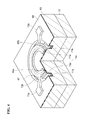
As a result of these steps, as illustrated in FIG. 5, a first substrate product SP1 for forming the surface-emitting semiconductor lasers is fabricated. In the present embodiment, the first substrate product SP1 is prepared by, for example, the above-described fabrication. The first substrate product SP1 has a first side SPU and a second side SPD. The first side SPU includes a device sections SCT arranged in an array and a street region STR that extends between the device sections SCT. The second side SPD exists on the opposite side to the first side SPU. In FIG. 5, the street region STR is drawn by broken lines for indicating the position of the street region STR.
As illustrated in FIG. 6, a mask 75 is formed on the first side SPU of the first substrate product SP1 in step S106. The mask 75 has device covering portions 75 a and a first opening 75 b. The device covering portions 75 a cover the respective device sections SCT. In the present embodiment, a single first opening 75 b is provided in the street region STR. Furthermore, the single first opening 75 b defines the device covering portions 75 a. The first opening 75 b surrounds the device covering portions 75 a. Referring to FIG. 7, the device covering portions 75 a of the mask 75 cover the device sections SCT. The mask 75 is made of a thick resist layer having a comparatively large thickness. A thickness (H75) of the resist layer ranges from 50 to 100 micrometers. According to the present embodiment, the thickness (H75) of the resist layer is, for example, 100 micrometers. Such a thick resist (photoresist) layer is formed by, for example, bonding a dry film resist or applying a negative resist (high-viscosity epoxy-based resist) for micro electromechanical systems (MEMS). Furthermore, a pattern of the thick resist layer is formed by, for example, contact exposure of the photoresist using a mask aligner or exposure of the photoresist to a reduced projection light using a stepper. Development is performed after the exposure. The size of the device sections SCT is, for example, 200-micrometer square. A width (W75) of the first opening 75 b ranges from 10 to 50 micrometers. According to the present embodiment, the width W75 is, for example, 10 micrometers. The width of the first opening 75 b is determined in consideration of the fact that the aspect ratio of the opening pattern that can be formed through exposure and development of the photoresist is 10. For example, for a resist layer having a thickness of 100 micrometers, the lower limit of the width is 10 micrometers. The width of the first opening 75 b is smaller than the width of an area to be cut away (for example, 60 micrometers) required for fabrication of semiconductor chips using a dicing saw. The device covering portions 75 a and the first opening 75 b of the mask 75 are provided outside a device area in which the array of the device sections SCT is included.
After the mask 75 has been formed on the first substrate product SP1, in step S107, the first side SPU of the first substrate product SP1 is etched using the mask 75, thereby a second substrate product SP2 is formed as illustrated in FIG. 8. The second substrate product SP2 has a deep groove 77 in a street region STR. The deep groove 77 penetrates through an epitaxial region and reaches the substrate 13. The device sections SCT have respective islands ILD. The second substrate product SP2 includes an array of the islands ILD separated from one another by the deep groove 77. The array of the islands ILD is defined by the deep groove 77. Furthermore, the deep groove 77 is formed so as to surround the device sections SCT.
For forming the deep groove 77, an etching apparatus ETCH2 as illustrated in FIG. 9 is prepared. The etching apparatus ETCH2 includes an inductive coupled plasma reactive ion etching (ICP-RIE) apparatus. Specifically, this etching apparatus ETCH2 includes a chamber 53, a lower electrode 54, an inductive coupling coil 55, a first high-frequency power source 56, and a second high-frequency power source 57. The chamber 53 is connected to a discharge pump P through a discharge channel 53 a. The chamber 53 is also connected to a gas introduction system 53 b for supplying gases GAS including a process gas and a raw-material gas. The chamber 53 includes a dielectric dome. Furthermore, the inductive coupling coil 55 is provided outside the dielectric dome of the chamber 53. The lower electrode 54 is provided in the chamber and allows the first substrate product SP1 to be placed thereon. The first high-frequency power source 56 is connected to the lower electrode 54 through a first impedance matching box 58. The second high-frequency power source 57 is connected to the inductive coupling coil 55 through a second impedance matching box 59. According to need, the lower electrode 54 is connected to a cooler 53 c for temperature adjustment of the substrate to be placed thereon for etching.
An example of the etching conditions for forming the deep groove 77
Etchant: either of BCl3 and Cl2 or mixture of BCl3 and Cl2
Flow ratios of process gas: BCl3/Cl2/Ar=30/40/30 sccm
The flow rate of chlorine (Cl2) is larger than that of boron trichloride (BCl3).
Etching rate: 5 to 6 micrometers/min
Detection of end point of deep groove: adjustment in accordance with etching time
The power conditions
BIAS power from the first high-frequency power source 56: 50 to 500 W
ICP power from the second high-frequency power source 57: 1000 W or larger
Temperature of substrate: preferably 25 degrees centigrade or lower
Under the above-described etching conditions, a recess having a depth of about 200 micrometers is formed in the street region.
After the first substrate product SP1 has been etched, the mask 75 is removed as illustrated in FIGS. 10A and 10B in step S108. The mask 75 is removed, for example, by one or some or all of an organic solvent, a remover (such as N-methyl-2-pyrrolidone, and an oxygen plasma treatment.
In step S109, after the mask 75 has been removed, as illustrated in FIGS. 11A, 11B, and 11C, a support member such as a sheet 79 is secured to a first side of the second substrate product SP2. The first side of the second substrate product SP2 adheres to the sheet 79 due to an adhering property of the surface of the sheet 79. The sheet 79 is, for example, ultra-violet (UV) curable dicing tape, a thermally removable sheet, or a thermosensitive adhesive sheet. The second substrate product SP2 is secured to the sheet 79 held by a dicing ring. The sheet 79 have the adhering property that may provide an adhering force resisting a pressure applied during the following polishing of the substrate. Due to the thickness of a pad electrode (projection of the pad electrode) provided on each of the islands ILD, contact of the sheet 79 with a device surface DF of the island ILD may be avoided as illustrated in an enlarged view of FIG. 11C.
After the second substrate product SP2 has been secured to the sheet 79, the thickness of the second substrate product SP2 is reduced in step S110 to such a thickness that the deep groove 77 in the first side of the second substrate product SP2 is exposed. Specifically, as illustrated in FIGS. 12A and 12B, a second side of the second substrate product SP2 is polished by using a polishing device 81. Broken lines illustrated in FIG. 12B indicate the shape of the second substrate product SP2. The sheet 79 firmly holds the islands ILD during the polishing.
In step S111, the second side of the second substrate product SP2 is polished so that the deep groove 77 is exposed. In this step S111, the device sections SCT (islands ILD) are separated from one another so as to form an array of semiconductor chips CP on the sheet 79 as illustrated in FIGS. 13A and 13B. Broken lines illustrated in FIG. 13B indicate the shape of the second substrate product SP2. Each of the semiconductor chips CP is a so-called surface-emitting semiconductor laser chip.
As illustrated in FIG. 14A, in step S112, the UV curable dicing tape is used as the sheet 79 in the embodiment. When the UV curable dicing tape is exposed to radiation of ultraviolet rays 83, the adhering property of the UV curable dicing tape is reduced. The semiconductor chips CP, that is, the surface-emitting semiconductor laser chips on the UV curable dicing tape are removed by using a collet from the UV curable dicing tape having been exposed to the ultraviolet radiation. As illustrated in FIG. 14B, the array of the semiconductor chips CP are transferred from the UV curable dicing tape to another support member such as a sheet 85 without removal using a collet. In the present embodiment, the sheet 85 is other UV curable dicing tape that has not been exposed to ultraviolet radiation yet. The other UV curable dicing tape supports the rear surfaces of the semiconductor chips CP, that is, the surface-emitting semiconductor laser chips. Due to the difference in adhering force between the UV curable dicing tape having been exposed to the ultraviolet radiation and the UV curable dicing tape not having been exposed to the ultraviolet radiation, the array of the semiconductor chips CP may be transferred from the sheet 79 to the sheet 85 while the array arrangement of the semiconductor chips CP is maintained. As illustrated in FIG. 14C, device surfaces of the array of the semiconductor chips CP face outward on the sheet 85. When the other UV curable dicing tape is exposed to ultraviolet radiation, an adhering property of the other UV curable dicing tape is reduced. The semiconductor chips CP (that is, the surface-emitting semiconductor laser chips) may be removed from the other UV curable dicing tape having been exposed to the ultraviolet radiation by gripping with the collet the surface sides of the semiconductor chips CP on the other UV curable dicing tape having been exposed to the ultraviolet radiation.
Through the above-described steps, a surface-emitting semiconductor laser 87 a illustrated in FIG. 15 are fabricated.
The surface-emitting semiconductor laser 87 a includes the substrate 13, the passivation film 69, a semiconductor structure 89, the first electrode 73 a, and the second electrode 73 b. The semiconductor structure 89 includes the stacked semiconductor layer 63. The stacked semiconductor layer 63 includes the semiconductor post 65. The semiconductor post 65 includes the first stacked semiconductor layer 15 for forming the first distributed Bragg reflector, the semiconductor region 17 including the active layer, and the second stacked semiconductor layer 19 for forming the second distributed Bragg reflector. The semiconductor structure 89 includes a first side 89 a, a second side 89 b opposite to the first side 89 a, and side surfaces (a first side surface 89 c, a second side surface 89 d, a third side surface 89 e, and a fourth side surface 89 f) that extend in a direction from the second side 89 b to the first side 89 a. The first electrode 73 a and the second electrode 73 b are provided on the first side 89 a of the semiconductor structure 89. The thickness of the substrate 13 of the surface-emitting semiconductor laser 87 a ranges, for example, from 100 to 200 micrometers.
The side surfaces 89 c, 89 d, 89 e, and 89 f reach the edges of the first side 89 a from the edges of the second side 89 b. The first side 89 a abuts the upper sides of the side surfaces 89 c, 89 d, 89 e, and 89 f The upper sides of the side surfaces 89 c, 89 d, 89 e, and 89 f have no chipping. Furthermore, the side surfaces 89 c, 89 d, 89 e, and 89 f are inclined by an angle ranging from 0 to 15 degrees relative to a reference surface perpendicular to the principal surface 13 a.
The side surfaces 89 c, 89 d, 89 e, and 89 f are formed by etching. Processing through etching allows the side surfaces to have a small surface roughness. In addition, processing through etching does not form chipping on the upper sides of the side surfaces. The surface-emitting semiconductor laser chip has the chipping-free device side surfaces having preferable surface roughness. The surface-emitting semiconductor laser chip requires no margins for chipping. Therefore, a device size of the surface-emitting semiconductor laser chip may be smaller than that having margins for chipping. The surface roughness Ra of the side surfaces 89 c, 89 d, 89 e, and 89 f is, for example, 100 nanometers or smaller.
In the method of fabricating a semiconductor optical device, as illustrated in FIG. 16A, a mask 76 having a comparatively small thickness may be formed before the mask 75 is formed on the first side SPU of the first substrate product SP1 according to need. The mask 76 includes a device covering portions 76 a. The edges of the device covering portions 76 a are positioned outside the edges of the device covering portions 75 a of the mask 75 to be fabricated in a step performed later. The device covering portions 76 a are formed so as to surround the device sections SCT. The mask 76 has a first opening 76 b being a single opening that defines the device covering portions 76 a. It is preferable that the first opening 76 b have a smaller width than the width of the street region STR defined by the mask 75. In the present embodiment, the mask 76 is formed of, for example, a resist. A resist thickness (H76) ranges from 3 to 10 micrometers. In the present embodiment, the resist thickness (H75) is, for example, 5 micrometers.
As illustrated in FIG. 16B, mesa structures MS are formed by etching the first side SPU of the first substrate product SP1 using the mask 76. This etching is performed under the conditions in which a weaker anisotropy than that of the etching using the mask 75 to be performed in a later step is exhibited.
The etching conditions using the thin mask 76
Power (ICP): from 50 to smaller than 1000 W
Power (BIAS): from 50 to 500 W
Flow ratios: BCl3/Cl2/Ar=20/10/70 sccm
The flow rate of boron chloride is larger than that of chlorine.
Process pressure: 1 Pa
The etching conditions using the mask 75
Power (ICP/BIAS): 1000 W or larger/50 to 500 W
Flow ratios: BCl3/Cl2/Ar=30/40/30 sccm
The flow rate of chlorine is larger than that of boron chloride.
Process pressure: 5 Pa
The surface roughness Ra of the side surfaces of the mesa structures MS is, for example, 100 nanometers or smaller.
The height of the mesa structures MS ranges from 5 to 10 micrometers. In the present embodiment, the height of the mesa structures MS is, for example, 10 micrometers. The side surfaces of the mesa structures MS have a tapered shape. The side surfaces of the mesa structures MS are inclined at an angle in a range from 60 to 70 degrees relative to the upper surface of the substrate 13. In the present embodiment, the inclined angle of the side surfaces of the mesa structures MS is, for example, about 70 degrees. The side surfaces of the mesa structures MS have lower edges located in the street region STR and upper edges located in the device sections SCT.
After the mesa structures MS have been formed, the mask 76 is removed as illustrated in FIG. 16C. After that, as illustrated in FIG. 16D, the mask 75 having been described is formed, and the deep groove is etched in the street region STR using the mask 75.
Before the etching using the mask 75, in a fabrication method of forming the mesa structures MS using the mask 76, surface-emitting semiconductor lasers 87 b are fabricated. Each of the surface-emitting semiconductor lasers 87 b is structured as illustrated in FIG. 17. The surface-emitting semiconductor laser 87 b has the same device structure as that of the surface-emitting semiconductor laser 87 a except for the shapes of the tapered side surfaces of the semiconductor structure 89. The semiconductor structure 89 includes the first side 89 a, the second side 89 b opposite to the first side 89 a, and the side surfaces 89 c, 89 d, 89 e, and 89 f that extend in a direction from the second side 89 b to the first side 89 a.
Each of the side surfaces 89 c, 89 d, 89 e, and 89 f has a lower side portion (first surface) near a corresponding one of the edges of the second side 89 b and an upper side portion (second surface) near a corresponding one of the edges of the first side 89 a. The first surface extends from the edge of the second side 89 b in a direction from the second side 89 b toward the first side 89 a. The second surface has a taper shape. The taper-shaped second surfaces form a loop shape so as to connect a device upper surface to the first surfaces and each have a width of 20 to 30 micrometers. The height of the mesa structure MS ranges from 5 to 10 micrometers. In the present embodiment, the height of the mesa structure MS is, for example, 10 micrometers. The first side 89 a abuts the upper sides of the taper-shaped upper portions of the side surfaces 89 c, 89 d, 89 e, and 89 f. The upper sides of the side surfaces 89 c, 89 d, 89 e, and 89 f, which are formed by etching using the mask 76, have no chipping. The side surfaces 89 c, 89 d, 89 e, and 89 f are formed by etching. Processing through etching allows the side surfaces to have a small surface roughness. In addition, processing through etching does not form chipping on the upper sides of the side surfaces. Since the surface-emitting semiconductor laser has the chipping-free device side surfaces having preferable surface roughness, it is not required to provide margins for chipping. Accordingly, the device size may be reduced. The surface roughness Ra of the taper-shaped upper side portions (side surfaces of the mesa structure MS) of the side surfaces 89 c, 89 d, 89 e, and 89 f is, for example, 100 nanometers or smaller. The taper-shaped upper side portions (side surfaces of the mesa structure MS) are each inclined at an angle in a range from 60 to 70 degrees relative to the upper surface of the substrate 13. In the present embodiment, this angle is, for example, about 70 degrees.
A contact portion of a pyramid-shaped collet is brought into contact with the side surfaces of the mesa structure MS having a normal taper shape. This reduces the possibility of breaking corners of the semiconductor chips. When handling the semiconductor chips with a collet, a super-hard pyramid-shaped collet can be used instead of a rubber collet. With the super-hard collet, inclination and misalignment of the semiconductor chips can be reduced. This can suppress positional deviation on target (destination) chips.
Examples of deviations using a rubber collet
Angular deviation: −10 to 20 degrees
Deviation in XY positions: −100 to +100 micrometers
Examples of deviations using a super-hard collet
Angular deviation: +/−5 degrees
Deviation in XY positions: −50 to +50 micrometers
An area to be cut away having a width of 60 micrometers is required for cutting with a dicing blade. With the method of fabricating according to the present embodiment, the width of the street region STR that allows etching to be performed may be reduced to 10 micrometers. With this method, the degree of concentration of the device sections per wafer can be increased. For example, when semiconductor chips of 200-micrometer square are fabricated on a three-inch wafer, the number of the semiconductor chips to be fabricated with the method of fabricating according to the present embodiment can be increased to 1.5 times the number of the semiconductor chips to be fabricated with a method using a dicing blade.
Although the principles of the present invention have been illustrated and described with the preferred embodiment, it is appreciated by those skilled in the art that arrangement and details of the present invention can be changed without departing from such principles. Accordingly, a right is claimed for all modifications and changes derived from the claims and the scope of the gist of the claims.

Claims (8)

What is claimed is:
1. A surface-emitting semiconductor laser comprising: a substrate; a first stacked semiconductor layer disposed on the substrate and including a first distributed Bragg reflector; an active layer disposed on the first stacked semiconductor layer; and a second stacked semiconductor layer disposed on the active layer and including a second distributed Bragg reflector; a first electrode; and a second electrode, the substrate, the first and second stacked semiconductor layers and the active layer providing a semiconductor structure with a first structure side, a second structure side opposite to the first structure side, and a side structure surface that extends from the second structure side to the first structure side, the side structure surface having an upper side free of chipping, the first electrode and the second electrode each being provided on the first structure side of the semiconductor structure, the semiconductor structure being formed by:
preparing a substrate product that includes a first side and a second side opposite to the first side, the first side including device sections arranged in an array and a street region extending between the device sections, at least one of the device sections including the first and second electrodes and the semiconductor structure for the surface-emitting semiconductor laser;
forming a first mask on the first side of the substrate product, the first mask having a pattern that includes device covering portions covering the respective device sections and an opening defining the device covering portions, the opening being provided in the street region;
etching the substrate product using the first mask so as to form a groove in the street region, the groove defining the device sections;
after removing the first mask, securing the first side of the substrate product to a first support member; and
after securing the first side of the substrate product to the first support member, forming an array of semiconductor chips on the first support member by removing part of the substrate product from the second side until the groove provided in the first side is exposed so as to separate the at least one device section including the first and second electrodes and the semiconductor structure from other device sections to provide the surface-emitting semiconductor laser.
2. The laser according to claim 1, wherein, in forming the array of the semiconductor chips on the first support member, the substrate product is partially removed by polishing the substrate product from its second side.
3. The laser according to claim 1, wherein the laser is a vertical cavity surface-emitting laser.
4. The laser according to claim 1, further comprising transferring the array of the semiconductor chips from the first support member to a second support member.
5. The laser according to claim 4, further comprising the step of separating each of the semiconductor chips from the second support member.
6. The laser according to claim 1, wherein the first mask includes a resist having a thickness of 100 micrometers or larger.
7. The laser according to claim 1, wherein the first mask includes a dry film resist.
8. The laser according to claim 1, wherein the semiconductor structure further is formed by:
forming a second mask having a smaller thickness than a thickness of the first mask on the substrate product; and
etching the substrate product using the second mask so as to form at least one mesa structure having inclined side surfaces,
wherein the inclined surfaces extend from boundaries between the at least one device section and the street region, and
wherein the first and second electrodes are provided on the at least one mesa structure.
US15/906,515 2017-04-03 2018-02-27 Method of fabricating semiconductor optical device and surface-emitting semiconductor laser Active US10170890B2 (en)

Applications Claiming Priority (2)

Application Number Priority Date Filing Date Title
JP2017073938A JP7059518B2 (en) 2017-04-03 2017-04-03 Method for manufacturing semiconductor optical devices
JP2017-073938 2017-04-03

Publications (2)

Publication Number Publication Date
US20180287346A1 US20180287346A1 (en) 2018-10-04
US10170890B2 true US10170890B2 (en) 2019-01-01

Family

ID=63670043

Family Applications (1)

Application Number Title Priority Date Filing Date
US15/906,515 Active US10170890B2 (en) 2017-04-03 2018-02-27 Method of fabricating semiconductor optical device and surface-emitting semiconductor laser

Country Status (2)

Country Link
US (1) US10170890B2 (en)
JP (1) JP7059518B2 (en)

Families Citing this family (2)

* Cited by examiner, † Cited by third party
Publication number Priority date Publication date Assignee Title
JP7251672B1 (en) * 2022-03-30 2023-04-04 信越半導体株式会社 Method for manufacturing light-emitting element
CN119921185B (en) * 2025-01-22 2025-10-03 苏州知行半导体科技有限公司 Preparation method and application of high-stability VCSEL device

Citations (4)

* Cited by examiner, † Cited by third party
Publication number Priority date Publication date Assignee Title
US20090032908A1 (en) * 2006-06-20 2009-02-05 Sony Corporation Semiconductor device and method of manufacturing it
US20090141766A1 (en) * 2007-11-06 2009-06-04 Yutaka Onishi Surface emitting semiconductor laser
US20110076854A1 (en) * 2009-09-30 2011-03-31 Furukawa Electric Co., Ltd. Method of manufacturing vertical-cavity surface emitting laser
US8189642B1 (en) * 2007-08-08 2012-05-29 Emcore Corporation VCSEL semiconductor device

Family Cites Families (11)

* Cited by examiner, † Cited by third party
Publication number Priority date Publication date Assignee Title
JPH05107757A (en) * 1991-10-19 1993-04-30 Canon Inc Photosensitive resin composition
JP2003158097A (en) * 2001-11-22 2003-05-30 Murata Mfg Co Ltd Semiconductor device and manufacturing method therefor
JP2003197881A (en) * 2001-12-27 2003-07-11 Seiko Epson Corp Semiconductor integrated circuit, method of manufacturing semiconductor integrated circuit, semiconductor element member, electro-optical device, electronic apparatus
JP4243075B2 (en) * 2002-06-13 2009-03-25 パナソニック株式会社 Semiconductor device and manufacturing method thereof
JP3723177B2 (en) * 2002-12-24 2005-12-07 株式会社東芝 Method for manufacturing optical element array
JP2005050997A (en) * 2003-07-28 2005-02-24 Matsushita Electric Ind Co Ltd Semiconductor element isolation method
JP4848638B2 (en) * 2005-01-13 2011-12-28 ソニー株式会社 Method for forming semiconductor device and method for mounting semiconductor device
JP5295783B2 (en) * 2007-02-02 2013-09-18 セミコンダクター・コンポーネンツ・インダストリーズ・リミテッド・ライアビリティ・カンパニー Semiconductor device
KR100882240B1 (en) * 2008-09-11 2009-02-25 (주)플러스텍 Nitride semiconductor light emitting device and manufacturing method
JP2014204014A (en) * 2013-04-08 2014-10-27 三菱電機株式会社 Semiconductor device and manufacturing method of the same
EP3127143A4 (en) * 2014-03-31 2017-11-29 Nanyang Technological University Methods of recycling substrates and carrier substrates

Patent Citations (5)

* Cited by examiner, † Cited by third party
Publication number Priority date Publication date Assignee Title
US20090032908A1 (en) * 2006-06-20 2009-02-05 Sony Corporation Semiconductor device and method of manufacturing it
JP5034662B2 (en) 2006-06-20 2012-09-26 ソニー株式会社 Surface emitting semiconductor laser and manufacturing method thereof
US8189642B1 (en) * 2007-08-08 2012-05-29 Emcore Corporation VCSEL semiconductor device
US20090141766A1 (en) * 2007-11-06 2009-06-04 Yutaka Onishi Surface emitting semiconductor laser
US20110076854A1 (en) * 2009-09-30 2011-03-31 Furukawa Electric Co., Ltd. Method of manufacturing vertical-cavity surface emitting laser

Also Published As

Publication number Publication date
US20180287346A1 (en) 2018-10-04
JP2018181887A (en) 2018-11-15
JP7059518B2 (en) 2022-04-26

Similar Documents

Publication Publication Date Title
US11342727B1 (en) Semiconductor laser diode on tiled gallium containing material
CN101685941B (en) Surface emitting laser and manufacturing method therefor
US5882988A (en) Semiconductor chip-making without scribing
TW201232977A (en) Vertical-cavity surface-emitting laser system and method for fabricating the same
US4940672A (en) Method of making monolithic integrated III-V type laser devices and silicon devices on silicon
JPH01120885A (en) Method of cutting off laser diodes formed in monolithic form
CN102403654A (en) Vertical resonant cavity surface emitting laser element and manufacturing method thereof
US10170890B2 (en) Method of fabricating semiconductor optical device and surface-emitting semiconductor laser
CN101160699A (en) High reliability etched facet photonic devices
TW201931457A (en) Light-emitting element manufacturing method
US12532574B2 (en) Method of preparing a device coupon for micro-transfer printing, device wafer including said device coupon, and optoelectronic device manufactured from said device wafer
US20210265806A1 (en) Selective-area growth of iii-v materials for integration with silicon photonics
CN111564755B (en) Vertical cavity surface emitting laser and manufacturing method thereof
US6335216B1 (en) Method for fabricating a semiconductor optical device having a ridge stripe
JP2002299761A (en) Surface emitting semiconductor light emitting device and method of manufacturing the same
WO2024217808A1 (en) Method for manufacturing a plurality of semiconductor chips
US8450128B2 (en) Method for producing semiconductor optical device and semiconductor optical device
US20200365445A1 (en) Susceptor and method of manufacturing semiconductor device
JP2020017650A (en) Method for manufacturing optical semiconductor device
JP4834920B2 (en) Manufacturing method of semiconductor device
US20240241317A9 (en) Coupon wafer and method of preparation thereof
US12276839B2 (en) Manufacturing a semiconductor structure
US11211523B2 (en) Method for manufacturing optical semiconductor device
US20240413614A1 (en) Manufacturable gallium and nitrogen containing coupled waveguide devices
CN111727535A (en) Quantum dot laser integrated on a silicon submount using mechanical features and through-silicon vias

Legal Events

Date Code Title Description
AS Assignment

Owner name: SUMITOMO ELECTRIC INDUSTRIES, LTD., JAPAN

Free format text: ASSIGNMENT OF ASSIGNORS INTEREST;ASSIGNOR:TSUJI, YUKIHIRO;REEL/FRAME:045052/0468

Effective date: 20180209

FEPP Fee payment procedure

Free format text: ENTITY STATUS SET TO UNDISCOUNTED (ORIGINAL EVENT CODE: BIG.); ENTITY STATUS OF PATENT OWNER: LARGE ENTITY

STCF Information on status: patent grant

Free format text: PATENTED CASE

MAFP Maintenance fee payment

Free format text: PAYMENT OF MAINTENANCE FEE, 4TH YEAR, LARGE ENTITY (ORIGINAL EVENT CODE: M1551); ENTITY STATUS OF PATENT OWNER: LARGE ENTITY

Year of fee payment: 4