US10157259B2 - Method and device for predicting reliability failure rate of semiconductor integrated circuit and method of manufacturing the semiconductor integrated circuit - Google Patents
Method and device for predicting reliability failure rate of semiconductor integrated circuit and method of manufacturing the semiconductor integrated circuit Download PDFInfo
- Publication number
- US10157259B2 US10157259B2 US15/407,365 US201715407365A US10157259B2 US 10157259 B2 US10157259 B2 US 10157259B2 US 201715407365 A US201715407365 A US 201715407365A US 10157259 B2 US10157259 B2 US 10157259B2
- Authority
- US
- United States
- Prior art keywords
- risk
- transistor
- transistors
- failure rate
- low
- Prior art date
- Legal status (The legal status is an assumption and is not a legal conclusion. Google has not performed a legal analysis and makes no representation as to the accuracy of the status listed.)
- Active, expires
Links
Images


Classifications
-
- G06F17/5081—
-
- G—PHYSICS
- G06—COMPUTING; CALCULATING OR COUNTING
- G06F—ELECTRIC DIGITAL DATA PROCESSING
- G06F30/00—Computer-aided design [CAD]
- G06F30/30—Circuit design
- G06F30/39—Circuit design at the physical level
- G06F30/398—Design verification or optimisation, e.g. using design rule check [DRC], layout versus schematics [LVS] or finite element methods [FEM]
-
- G—PHYSICS
- G01—MEASURING; TESTING
- G01R—MEASURING ELECTRIC VARIABLES; MEASURING MAGNETIC VARIABLES
- G01R31/00—Arrangements for testing electric properties; Arrangements for locating electric faults; Arrangements for electrical testing characterised by what is being tested not provided for elsewhere
- G01R31/28—Testing of electronic circuits, e.g. by signal tracer
- G01R31/2851—Testing of integrated circuits [IC]
- G01R31/2855—Environmental, reliability or burn-in testing
- G01R31/2856—Internal circuit aspects, e.g. built-in test features; Test chips; Measuring material aspects, e.g. electro migration [EM]
-
- G06F17/5036—
-
- G—PHYSICS
- G06—COMPUTING; CALCULATING OR COUNTING
- G06F—ELECTRIC DIGITAL DATA PROCESSING
- G06F30/00—Computer-aided design [CAD]
- G06F30/30—Circuit design
- G06F30/36—Circuit design at the analogue level
- G06F30/367—Design verification, e.g. using simulation, simulation program with integrated circuit emphasis [SPICE], direct methods or relaxation methods
-
- G—PHYSICS
- G06—COMPUTING; CALCULATING OR COUNTING
- G06F—ELECTRIC DIGITAL DATA PROCESSING
- G06F2119/00—Details relating to the type or aim of the analysis or the optimisation
- G06F2119/18—Manufacturability analysis or optimisation for manufacturability
-
- G06F2217/12—
-
- Y—GENERAL TAGGING OF NEW TECHNOLOGICAL DEVELOPMENTS; GENERAL TAGGING OF CROSS-SECTIONAL TECHNOLOGIES SPANNING OVER SEVERAL SECTIONS OF THE IPC; TECHNICAL SUBJECTS COVERED BY FORMER USPC CROSS-REFERENCE ART COLLECTIONS [XRACs] AND DIGESTS
- Y02—TECHNOLOGIES OR APPLICATIONS FOR MITIGATION OR ADAPTATION AGAINST CLIMATE CHANGE
- Y02P—CLIMATE CHANGE MITIGATION TECHNOLOGIES IN THE PRODUCTION OR PROCESSING OF GOODS
- Y02P90/00—Enabling technologies with a potential contribution to greenhouse gas [GHG] emissions mitigation
- Y02P90/02—Total factory control, e.g. smart factories, flexible manufacturing systems [FMS] or integrated manufacturing systems [IMS]
Definitions
- Embodiments of the disclosure relate to a method of analyzing the reliability of a semiconductor circuit, and more particularly, to a method of predicting the failure rate of a circuit, thereby reducing simulation time.
- SPICE Simulation program with integrated circuit emphasis
- Reliability simulations using SPICE are performed with regard to the area, operating voltage and temperature of every transistor in a circuit. At this time, the simulation takes a long time.
- a method of predicting a failure rate of a semiconductor integrated circuit includes receiving a circuit netlist corresponding to circuit defining data, which defines a connection relation, input, output, size, type and operating temperature of each of a plurality of transistors included in the semiconductor integrated circuit. Low-risk transistors having a low-failure probability among the plurality of transistors are detected and filtered out based on the circuit netlist. Failure rates are calculated of respective high-risk transistors other than the low-risk transistors among the plurality of transistors. A total failure rate of the semiconductor integrated circuit is calculated based on the failure rates of the respective high-risk transistors.
- a device for predicting a failure rate of a semiconductor integrated circuit includes a memory configured to store a program code and a circuit netlist which defines a connection relation, input, output, size, type and operating temperature of each of a plurality of transistors included in the semiconductor integrated circuit.
- a processor executes the program code, detects low-risk transistors having a low-failure probability among the plurality of transistors based on the circuit netlist, and calculates failure rates of respective high-risk transistors other than the low-risk transistors among the plurality of transistors.
- a method of manufacturing a semiconductor integrated circuit includes: a) receiving a circuit netlist defining connection relations among transistors of the semiconductor integrated circuit and an operating parameter of each of the transistors; b) identifying, among the transistors, high-risk transistors having high failure probabilities based on the operating parameters of the transistors defined by the circuit netlist; c) calculating a failure rate of each of the high-risk transistors; d) calculating a total failure rate of the semiconductor integrated circuit based on the calculated failure rates of the high-risk transistors; e) comparing the total failure rate to a reference value to determine whether the circuit netlist satisfies a design criterion; and f) manufacturing the semiconductor integrated circuit based upon the circuit netlist in response to determining that the circuit netlist satisfies the design criterion.
- FIG. 1 is a flowchart of a method of verifying the design of a semiconductor integrated circuit according to some embodiments of the disclosure
- FIG. 2 is a flowchart of a method of predicting a failure rate according to some embodiments of the disclosure
- FIG. 3 is a schematic graph of a maximum voltage and a typical voltage according to some embodiments of the disclosure.
- FIG. 4 is a diagram of the waveform of an operating voltage according to some embodiments of the disclosure.
- FIGS. 5A and 5B are diagrams illustrating the gate-source voltage and gate-drain voltage of a P-channel metal oxide semiconductor (PMOS) transistor and an N-channel MOS (NMOS) transistor, respectively;
- PMOS metal oxide semiconductor
- NMOS N-channel MOS
- FIG. 6 is a flowchart of a method of predicting a failure rate according to other embodiments of the disclosure.
- FIG. 7 is a flowchart of a method of predicting a failure rate according to further embodiments of the disclosure.
- FIG. 8 is a block diagram of a failure rate prediction device according to some embodiments of the disclosure.
- FIG. 1 is a flowchart of a method of verifying the design of a semiconductor integrated circuit according to some embodiments of the disclosure. Referring to FIG. 1 , a reliability failure rate is predicted at the stage of designing a semiconductor integrated circuit (IC) and the design of the IC is modified according to the prediction result, so that the circuit with secured reliability can be fabricated.
- IC semiconductor integrated circuit
- a circuit is designed by a circuit designer in operation S 100 and a reliability simulation is performed on the circuit in operation S 200 .
- a reliability failure rate may be calculated as the result of the reliability simulation.
- the reliability failure rate may be compared with a predetermined criterion in operation S 400 .
- the method returns to operation S 100 .
- a procedure for (S 100 ) modifying the circuit design, (S 200 ) performing the reliability simulation on the circuit, and (S 400 ) determining whether the reliability failure rate meets the criterion is repeated.
- a circuit with a secured reliability is fabricated by using a method of predicting a reliability failure rate and modifying the design of an IC until the predicted result meets the predetermined criterion.
- Hot carrier injection (HCI), bias temperature instability (BTI), and time dependent dielectric breakdown (TDDB) are representative parameters which determine the reliability duration of a transistor.
- TDDB is a parameter which features a TDDB failure of a MOS transistor.
- a failure rate may be predicted (or calculated) by performing a simulation using a simulation model for each of the parameters and simulation conditions may be changed or a circuit may be improved when the predicted (or calculated) failure rate is higher than a criterion value, so that a failure can be prevented at a design stage.
- FIG. 2 is a flowchart of a method of predicting a failure rate according to some embodiments of the disclosure.
- FIG. 2 illustrates a method of predicting a TDDB failure rate, but the disclosure is not restricted to the current embodiments.
- the method may also be used to predict a different type of failure rate (e.g., an HCI failure rate or a BTI failure rate).
- a failure rate prediction device receives a circuit netlist necessary for a simulation in operation S 210 .
- the failure rate prediction device is also called a failure rate calculation device and is a device which predicts or calculates a failure rate by performing a simulation of a semiconductor circuit.
- the failure rate prediction device may include at least one processor which performs a simulation program. The structure and operations of the failure rate prediction device will be described with reference to FIG. 8 later.
- the circuit netlist is data which defines the operating condition (e.g., an operating temperature) of a semiconductor circuit (hereinafter, referred to as a “target circuit” or a “circuit”) subjected to the simulation and the connection relation, input signal, output signal, size (e.g., width and length of a transistor) and type (e.g., PMOS or NMOS) of each of transistors included in the target circuit.
- the circuit netlist may also be referred to as “circuit defining data.”
- the circuit netlist may be input to or stored in the failure rate prediction device in a form of a file with a predetermined format.
- An area A use and a type of each transistor during the operation of the circuit are calculated from the circuit netlist in operation S 220 .
- the area A use of the transistor may be calculated by extracting the width and length of the transistor.
- the type of the transistor may be divided into a P-channel metal oxide semiconductor (PMOS) transistor and an N-channel MOS (NMOS) transistor.
- An operating temperature T use is also calculated from the circuit netlist in operation S 230 . The operating temperature T use may be applied to all the transistors of the target circuit.
- low-risk transistors are filtered in operation S 240 .
- low-risk transistors having a low failure probability are detected in the transistors of the target circuit based on the circuit netlist and filtered out. Whether a transistor is a low-risk transistor may be determined using a method described below.
- an operating voltage V use of the transistor is set to a maximum voltage V max .
- the maximum voltage V max may be a highest voltage which is acceptable in circuit processes or applicable during the operation of the circuit.
- the maximum voltage V use is a voltage used in a worst case where a transistor operates in worst conditions.
- FIG. 3 is a schematic graph of the maximum voltage V max and a typical voltage V typ according to some embodiments of the disclosure. Referring to FIG. 3 , the maximum voltage V max may be a fixed voltage which has been set in advance.
- a failure rate F tr of the transistor is calculated with the operating voltage V use set to the maximum voltage V max .
- the failure rate F tr is calculated using a predetermined equation or algorithm.
- the failure rate F tr calculated with the operating voltage V use set to the maximum voltage V max is referred to as a worst-case failure rate or maximum failure rate of the transistor.
- a maximum failure rate F tr,max is lower than a failure rate limit (hereinafter, referred to as a first target failure rate F target , the transistor is determined as a low-risk transistor.
- the maximum failure rate F tr,max is equal to or higher than the first target failure rate F target , the transistor is not a low-risk transistor. Accordingly, the operating voltage V use is computed from the circuit netlist in operation S 250 .
- FIG. 4 is a diagram of the waveform of the operating voltage V use according to some embodiments of the disclosure.
- the operating voltage V use may change over time and may be computed a plurality of times during a predetermined period T p .
- the operating voltage V use may be a gate voltage of a transistor.
- a voltage at a gate of a transistor may be compared with a threshold voltage (Vth) at intervals of a predetermined minute time ⁇ t to determine an operating mode (e.g., an inversion mode or an accumulation mode) of the transistor and a larger value between a gate-source potential difference and a gate-drain potential difference may be determined as the operating voltage V use according to the operating mode.
- the operating voltage V use of a transistor may be computed using a method described below.
- FIGS. 5A and 5B are diagrams illustrating the gate-to-source voltage V gs and the gate-to-drain voltage V gd of PMOS transistors T 1 and T 2 and an NMOS transistor T 3 .
- the operating mode of the transistor is set to the inversion mode and the greater one between the gate-to-source voltage V gs and the gate-to-drain voltage V gd is set as the operating voltage V use .
- the operating mode of the transistor is set to the accumulation mode and the greater one between the absolute value of the gate-to-source voltage V gs and the absolute value of the gate-to-drain voltage V gd is set as the operating voltage V use .
- the operating mode of the transistor is set to the inversion mode and the lesser value between the gate-to-source voltage V gs and the gate-to-drain voltage V gd is set as the operating voltage V use .
- the operating mode of the transistor is set to the accumulation mode and the greater value between the gate-to-source voltage V gs and the gate-to-drain voltage V gd is set as the operating voltage V use .
- the operating voltage V use may be computed using the above-described method at intervals of the predetermined minute time ⁇ t during the predetermined period T p .
- the waveform of the operating voltage V use computed at intervals of the minute time ⁇ t may appear as illustrated in FIG. 4 .
- the operating voltage V use which changes over time may be obtained, as shown in FIG. 4 .
- a failure rate factor Fa(t) corresponding to each minute time ⁇ t may be calculated using the operating voltage V use computed at intervals of the minute time ⁇ t and the failure rate (e.g., TDDB failure rate) F tr of the transistor may be calculated using the failure rate factor Fa(t) at each minute time ⁇ t in operation S 260 .
- the calculation of the failure rate factor Fa(t) using the operating voltage V use and the calculation of the failure rate F tr using the failure rate factor Fa(t) may be performed using a predetermined equation or algorithm.
- a failure rate is calculated based on a plurality of operating voltages computed at minute time intervals with respect to each high-risk transistor (i.e., a transistor which is not a low-risk transistor). Accordingly, it may take a long time to compute the waveform of the operating voltage V use illustrated in FIG. 4 .
- a failure rate may be calculated on an assumption that the typical voltage V typ is applied to the gate of the transistor during the predetermined period T p , as shown in FIG. 3 .
- the failure rate may be calculated on an assumption that the operating voltage V use of a low-risk transistor is the typical voltage V typ .
- the typical voltage V typ is a voltage at which a target circuit usually operates and may be lower than the maximum voltage V max .
- the typical voltage V typ may be a predetermined fixed voltage. Accordingly, for a low-risk transistor, the waveform illustrated in FIG. 4 may not be computed, but a failure rate may be calculated based on the typical voltage V typ , so that it may take less time to calculate the failure rate as compared to a high-risk transistor.
- Operations S 220 through S 260 may be performed on all transistors included in a target circuit.
- the number of transistors included in the target circuit is N which is a natural number of at least 2.
- Each of the N transistors included in the target circuit may be classified into either a high-risk transistor or a low-risk transistor. It is assumed that the number of high-risk transistors among the N transistors is P and the number of low-risk transistors among the N transistors is N ⁇ P.
- a simulation result including the failure rate of the target circuit may be output in a file format in operation S 270 .
- FIG. 6 is a flowchart of a method of predicting a failure rate according to other embodiments of the disclosure.
- a method of predicting a TDDB failure rate is illustrated in FIG. 6
- the method may also be used to predict a different type of failure rate (e.g., an HCI failure rate or a BTI failure rate).
- the method illustrated in FIG. 6 may be performed by a failure rate prediction device which will be described later.
- the method illustrated in FIG. 6 is similar to the method illustrated in FIG. 2 . To avoid redundancy, the description made above with reference to FIG. 2 will be omitted.
- the operating temperature T use is calculated in operation S 310 .
- the operating temperature T use may be extracted from the circuit operating conditions in the circuit netlist, as described above.
- the circuit netlist may be input to or stored in the failure rate prediction device in a predetermined file format.
- the operating temperature T use may be applied to all the transistors of the target circuit.
- a variable “j” for identifying a target transistor may be initialized to “1” before operation S 320 in other embodiments.
- Operation S 320 is the same as operation S 220 , thus the detailed description is omitted.
- the operating voltage V use of the transistor is set to the maximum voltage V max and a failure rate F tr of the transistor at the worst case (i.e., a maximum failure rate) is calculated in operation S 330 .
- the maximum failure rate F tr is compared with the first target failure rate F target in operation S 340 .
- the current transistor is determined to be a low-risk transistor. Accordingly, the operating voltage V use of the transistor is set to the typical voltage V typ and the typical failure rate F tr of the transistor is re-calculated in operation S 360 . Thereafter, the typical failure rates F tr for all low-risk transistors are accumulated in operation S 370 .
- the current transistor is determined as a high-risk transistor. Accordingly, a configuration necessary to calculate the operating voltage V use of the transistor at intervals of the minute time ⁇ t during the predetermined period T p is set in operation S 350 . Commands for computing the waveform of the operating voltage V use of the transistor may be set in operation S 350 .
- the failure rate prediction device may interpret the commands, compute the waveform of the operating voltage V use of the high-risk transistor, and calculate the failure rate of the high-risk transistor using the waveform of the operating voltage V use .
- the failure rate of the transistor may be calculated based on a plurality of operating voltages calculated at intervals of the minute time At in operation S 350 . Similar to operation S 370 , the failure rates of respective high-risk transistors may be summed up in operation S 350 .
- a failure rate has been calculated with respect to every transistor in the target circuit is determined in operation S 380 .
- “j” may be compared with N which is the number of all transistors included in the target circuit in order to determine whether a failure rate has been calculated with respect to every transistor.
- “j” is increased by 1 in operation S 355 and the method is repeated from operation S 320 .
- operations S 320 through S 380 may be repeated until failure rates of all transistors included in the target circuit are calculated.
- the failure rate of the target circuit i.e., the total failure rate F total may be calculated using Equation 1.
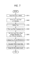
- FIG. 7 is a flowchart of a method of predicting a failure rate according to further embodiments of the disclosure.
- the method illustrated in FIG. 7 may be performed by the failure rate prediction device which will be described later.
- the method illustrated in FIG. 7 is similar to the method illustrated in FIG. 2 . Thus, to avoid redundancy, the description will be focused on the differences between the methods.
- the method illustrated in FIG. 7 may further include an operation S 245 of setting a command file for computing the waveform of the operating voltage V use of a high-risk transistor as compared to the method illustrated in FIG. 2 .
- the failure rate prediction device ( 1 in FIG. 8 ) may calculate the failure rate F total of the target circuit using at least two simulators.
- the at least two simulators may include a first simulator which classifies each of the transistors included in the target circuit as either a low-risk transistor or a high-risk transistor and a second simulator which computes the waveform of the operating voltage V use and calculates a failure rate.
- the first simulator may perform operations S 210 through S 240 to classify each of the transistors in the target circuit as either a low-risk transistor or a high-risk transistor.
- the first simulator may also generate the command file for computing the waveform of the operating voltage V use of transistors classified as high-risk transistors in operation S 245 .
- the command file may include information for identifying the transistors classified as high-risk transistors.
- the command file may be used as an input file of the second simulator.
- the second simulator may compute the waveform of the operating voltage V use of each high-risk transistor based on the command file in operation S 250 .
- the second simulator may also calculate the failure rate (e.g., TDDB failure rate) F tr of the high-risk transistor using the operating voltage V use in operation S 260 .
- TDDB failure rate e.g., TDDB failure rate
- F tr the failure rate of the high-risk transistor using the operating voltage V use in operation S 260 .
- a failure rate may be calculated based on an assumption that the typical voltage V typ is applied to the gate of the transistor during the predetermined period T p , as shown in FIG. 3 .
- the total failure rate F total of N transistors, i.e., the failure rate of the target circuit may be calculated using Equation 1.
- FIG. 8 is a block diagram of the failure rate prediction device 1 according to some embodiments of the disclosure.
- the failure rate prediction device 1 may be implemented as a computer such as a personal computer (PC), a tablet computer, or a server.
- the failure rate prediction device 1 may include a processor 10 , a memory 20 , a display device 30 , and a user interface 40 .
- the processor 10 controls the overall operation of the failure rate prediction device 1 .
- the processor 10 may process or execute programs and/or data stored in the memory 20 .
- the processor 10 may execute a simulation program stored in the memory 20 to perform the method of predicting a failure rate of a semiconductor IC according to the embodiments of the disclosure described with reference to FIGS. 2 through 7 above.
- the processor 10 may also read a circuit netlist file from the memory 20 and control the circuit netlist file to be used as an input of the simulation program.
- the processor 10 may be implemented as a multi-core processor.
- the multi-core processor is a single computing component with two or more independent actual processors (referred to as cores). Each of the processors may read and execute program instructions.
- the processor 10 may be called a controller, a microcontroller, a microprocessor, a microcomputer, or an application processor.
- the processor 10 may be implemented in hardware, firmware, software, or a combination thereof.
- the memory 20 may store a program (e.g., a simulator) and data (e.g., a circuit netlist) used to perform a method of predicting a failure rate of a semiconductor IC according to some embodiments of the disclosure.
- the memory 20 may be formed of non-volatile memory, volatile memory, or a combination thereof.
- the memory 20 may include read-only memory (ROM) (not shown), random access memory (RAM) (not shown), and a storage device (not shown).
- the ROM may store permanent programs and/or data.
- the ROM may be implemented as erasable programmable ROM (EPROM) or electrically erasable programmable ROM (EEPROM).
- the RAM may temporarily store programs, data, or instructions.
- the programs and/or data stored in the storage device may be temporarily stored in the RAM according to the control of the processor 10 or a booting code stored in the ROM.
- the RAM may be implemented as dynamic RAM (DRAM) or static RAM (SRAM).
- the user interface 40 is a device which allows a user of the failure rate prediction device 1 to interface with the failure rate prediction device 1 .
- the user interface 40 may include various types of input devices such as a button, a keypad, a dial, a touch screen, an audio input interface, an image/video input interface, and a sensor data input interface.
- the display device 30 may display image/video signals to a user according to the control of the processor 10 .
- the display device 30 may output data and/or results (e.g., simulation results) while a method of predicting a failure rate according to some embodiments is being performed.
- the failure rate prediction result PR calculated by the failure rate prediction device 1 may be transmitted to the circuit design device 3 .
- the reliability failure rate data PR calculated by the failure rate prediction device 1 or result data PR obtained by comparing the reliability failure rate with the predetermined criterion can be transmitted to the circuit design device 3 .
- the circuit design device 3 is a device for designing a circuit or modifying a designed circuit, and may have a configuration similar to those of the failure rate prediction device 1 .
- the circuit design device 3 can modify the circuit design based on the failure rate prediction result PR.
- the circuit design device 3 can perform circuit design using a specific tool (e.g., CAD: Computer Aided Design) for circuit design.
- the circuit design device 3 can modify the connection relationship, input, output or layout of the circuit elements based on the failure rate prediction result PR.
- the circuit design device 3 may provide a modified circuit design result CDR to the failure rate prediction device 1 .
- the circuit design is modified by the circuit design device 3
- the circuit netlist is modified.
- the failure rate prediction device 1 predicts the reliability failure rate again based on the modified circuit netlist, and when the re-predicted reliability failure rate satisfies the predetermined criterion, the designed circuit is finally fabricated.
- the execution time of a simulation is reduced without a decrease of the accuracy of the simulation when an operating voltage at each node in a circuit is calculated and reliability (i.e., duration, e.g., TDDB) and a failure rate (ppm) are calculated using the operating voltage. Since a TDDB failure probability increases as the area of gate oxide of a transistor increases in a circuit, a maximum failure rate is calculated in a worst case and a low-risk transistor is filtered out based on the maximum failure rate. Since verification is performed focusing on high-risk transistors, simulation time is reduced and fast feedback is given to a design, so that time (e.g., design and simulation time) taken before a circuit is actually fabricated is reduced. As a result, circuit design and fabrication costs are reduced.
- reliability i.e., duration, e.g., TDDB
- ppm failure rate
- circuits may, for example, be embodied in one or more semiconductor chips, or on substrate supports such as printed circuit boards and the like.
- circuits constituting a block may be implemented by dedicated hardware, or by a processor (e.g., one or more programmed microprocessors and associated circuitry), or by a combination of dedicated hardware to perform some functions of the block and a processor to perform other functions of the block.
- a processor e.g., one or more programmed microprocessors and associated circuitry
- Each block of the embodiments may be physically separated into two or more interacting and discrete blocks without departing from the scope of the disclosure.
- the blocks of the embodiments may be physically combined into more complex blocks without departing from the scope of the disclosure.
Abstract
A method for predicting a failure rate of a semiconductor integrated circuit includes receiving a circuit netlist corresponding to circuit defining data, which defines a connection relation, input, output, size, type and operating temperature of each transistor of a plurality of transistors included in the semiconductor integrated circuit. Low-risk transistors having a low-failure probability among the plurality of transistors are detected and filtered out based on the circuit netlist. Failure rates are calculated of respective high-risk transistors other than the low-risk transistors among the plurality of transistors. A total failure rate of the semiconductor integrated circuit is calculated based on the failure rates of the respective high-risk transistors.
Description
This application claims priority under 35 U.S.C. § 119(a) from Korean Patent Application No. 10-2016-0007263 filed on Jan. 20, 2016, the disclosure of which is hereby incorporated by reference in its entirety.
Embodiments of the disclosure relate to a method of analyzing the reliability of a semiconductor circuit, and more particularly, to a method of predicting the failure rate of a circuit, thereby reducing simulation time.
With the increase of scaling and variation in semiconductor circuit processes, a reliability margin is decreasing. Accordingly, it is important to analyze various types of reliability parameters and design a circuit based on the analysis during circuit design. For instance, it is necessary to perform a reliability simulation during circuit design in order to reduce risks after the circuit is manufactured and to meet standard requirements so that a circuit is designed to conform to the standard. Simulation program with integrated circuit emphasis (SPICE) is a representative of simulation programs for electronic circuits.
Reliability simulations using SPICE are performed with regard to the area, operating voltage and temperature of every transistor in a circuit. At this time, the simulation takes a long time.
According to some embodiments of the disclosure, there is provided a method of predicting a failure rate of a semiconductor integrated circuit. The method includes receiving a circuit netlist corresponding to circuit defining data, which defines a connection relation, input, output, size, type and operating temperature of each of a plurality of transistors included in the semiconductor integrated circuit. Low-risk transistors having a low-failure probability among the plurality of transistors are detected and filtered out based on the circuit netlist. Failure rates are calculated of respective high-risk transistors other than the low-risk transistors among the plurality of transistors. A total failure rate of the semiconductor integrated circuit is calculated based on the failure rates of the respective high-risk transistors.
According to other embodiments of the disclosure, there is provided a device for predicting a failure rate of a semiconductor integrated circuit. The device includes a memory configured to store a program code and a circuit netlist which defines a connection relation, input, output, size, type and operating temperature of each of a plurality of transistors included in the semiconductor integrated circuit. A processor executes the program code, detects low-risk transistors having a low-failure probability among the plurality of transistors based on the circuit netlist, and calculates failure rates of respective high-risk transistors other than the low-risk transistors among the plurality of transistors.
According to other embodiments of the disclosure, there is provided a method of manufacturing a semiconductor integrated circuit. The manufacturing method includes: a) receiving a circuit netlist defining connection relations among transistors of the semiconductor integrated circuit and an operating parameter of each of the transistors; b) identifying, among the transistors, high-risk transistors having high failure probabilities based on the operating parameters of the transistors defined by the circuit netlist; c) calculating a failure rate of each of the high-risk transistors; d) calculating a total failure rate of the semiconductor integrated circuit based on the calculated failure rates of the high-risk transistors; e) comparing the total failure rate to a reference value to determine whether the circuit netlist satisfies a design criterion; and f) manufacturing the semiconductor integrated circuit based upon the circuit netlist in response to determining that the circuit netlist satisfies the design criterion.
The above and other features and advantages of the disclosure will become more apparent by describing in detail exemplary embodiments thereof with reference to the attached drawings in which:
In detail, a circuit is designed by a circuit designer in operation S100 and a reliability simulation is performed on the circuit in operation S200. A reliability failure rate may be calculated as the result of the reliability simulation.
The reliability failure rate may be compared with a predetermined criterion in operation S400. When the reliability failure rate is equal to or higher than the criterion (i.e., in case of NO) in operation S400, the method returns to operation S100. In other words, a procedure for (S100) modifying the circuit design, (S200) performing the reliability simulation on the circuit, and (S400) determining whether the reliability failure rate meets the criterion is repeated.
When the reliability failure rate is lower than the criterion (i.e., in case of YES) in operation S400, the circuit is finally fabricated in operation S500. Therefore, according to the embodiments of the disclosure, a circuit with a secured reliability is fabricated by using a method of predicting a reliability failure rate and modifying the design of an IC until the predicted result meets the predetermined criterion.
Hot carrier injection (HCI), bias temperature instability (BTI), and time dependent dielectric breakdown (TDDB) are representative parameters which determine the reliability duration of a transistor. TDDB is a parameter which features a TDDB failure of a MOS transistor. A failure rate may be predicted (or calculated) by performing a simulation using a simulation model for each of the parameters and simulation conditions may be changed or a circuit may be improved when the predicted (or calculated) failure rate is higher than a criterion value, so that a failure can be prevented at a design stage.
Referring to FIG. 2 , a failure rate prediction device receives a circuit netlist necessary for a simulation in operation S210. The failure rate prediction device is also called a failure rate calculation device and is a device which predicts or calculates a failure rate by performing a simulation of a semiconductor circuit. The failure rate prediction device may include at least one processor which performs a simulation program. The structure and operations of the failure rate prediction device will be described with reference to FIG. 8 later.
The circuit netlist is data which defines the operating condition (e.g., an operating temperature) of a semiconductor circuit (hereinafter, referred to as a “target circuit” or a “circuit”) subjected to the simulation and the connection relation, input signal, output signal, size (e.g., width and length of a transistor) and type (e.g., PMOS or NMOS) of each of transistors included in the target circuit. The circuit netlist may also be referred to as “circuit defining data.” The circuit netlist may be input to or stored in the failure rate prediction device in a form of a file with a predetermined format.
An area Ause and a type of each transistor during the operation of the circuit are calculated from the circuit netlist in operation S220. The area Ause of the transistor may be calculated by extracting the width and length of the transistor. The type of the transistor may be divided into a P-channel metal oxide semiconductor (PMOS) transistor and an N-channel MOS (NMOS) transistor. An operating temperature Tuse is also calculated from the circuit netlist in operation S230. The operating temperature Tuse may be applied to all the transistors of the target circuit.
Thereafter, low-risk transistors are filtered in operation S240. In detail, low-risk transistors having a low failure probability are detected in the transistors of the target circuit based on the circuit netlist and filtered out. Whether a transistor is a low-risk transistor may be determined using a method described below.
Firstly, an operating voltage Vuse of the transistor is set to a maximum voltage Vmax. The maximum voltage Vmax may be a highest voltage which is acceptable in circuit processes or applicable during the operation of the circuit. In other words, the maximum voltage Vuse is a voltage used in a worst case where a transistor operates in worst conditions. FIG. 3 is a schematic graph of the maximum voltage Vmax and a typical voltage Vtyp according to some embodiments of the disclosure. Referring to FIG. 3 , the maximum voltage Vmax may be a fixed voltage which has been set in advance.
A failure rate Ftr of the transistor is calculated with the operating voltage Vuse set to the maximum voltage Vmax. The failure rate Ftr is calculated using a predetermined equation or algorithm. The failure rate Ftr calculated with the operating voltage Vuse set to the maximum voltage Vmax is referred to as a worst-case failure rate or maximum failure rate of the transistor.
When a maximum failure rate Ftr,max is lower than a failure rate limit (hereinafter, referred to as a first target failure rate Ftarget, the transistor is determined as a low-risk transistor. When the maximum failure rate Ftr,max is equal to or higher than the first target failure rate Ftarget, the transistor is not a low-risk transistor. Accordingly, the operating voltage Vuse is computed from the circuit netlist in operation S250.
Firstly, a gate-to-source voltage Vgs and a gate-to-drain voltage Vgd of the transistor are extracted. FIGS. 5A and 5B are diagrams illustrating the gate-to-source voltage Vgs and the gate-to-drain voltage Vgd of PMOS transistors T1 and T2 and an NMOS transistor T3.
For a PMOS transistor, whether the gate-to-source voltage Vgs is at least the Vth is determined and whether the gate-to-drain voltage Vgd is at least the Vth is determined. When any one of the gate-to-source voltage Vgs and the gate-to-drain voltage Vgd is at least the Vth, the operating mode of the transistor is set to the inversion mode and the greater one between the gate-to-source voltage Vgs and the gate-to-drain voltage Vgd is set as the operating voltage Vuse. When both of the gate-to-source voltage Vgs and the gate-to-drain voltage Vgd are less than the Vth, the operating mode of the transistor is set to the accumulation mode and the greater one between the absolute value of the gate-to-source voltage Vgs and the absolute value of the gate-to-drain voltage Vgd is set as the operating voltage Vuse.
For an NMOS transistor, whether the gate-to-source voltage Vgs is at most the Vth is determined and whether the gate-to-drain voltage Vgd is at most the Vth is determined. When any one of the gate-to-source voltage Vgs and the gate-to-drain voltage Vgd is at most the Vth, the operating mode of the transistor is set to the inversion mode and the lesser value between the gate-to-source voltage Vgs and the gate-to-drain voltage Vgd is set as the operating voltage Vuse. When both of the gate-to-source voltage Vgs and the gate-to-drain voltage Vgd are greater than the Vth, the operating mode of the transistor is set to the accumulation mode and the greater value between the gate-to-source voltage Vgs and the gate-to-drain voltage Vgd is set as the operating voltage Vuse.
The operating voltage Vuse may be computed using the above-described method at intervals of the predetermined minute time Δt during the predetermined period Tp. The waveform of the operating voltage Vuse computed at intervals of the minute time Δt may appear as illustrated in FIG. 4 . In other words, the operating voltage Vuse which changes over time may be obtained, as shown in FIG. 4 .
A failure rate factor Fa(t) corresponding to each minute time Δt may be calculated using the operating voltage Vuse computed at intervals of the minute time Δt and the failure rate (e.g., TDDB failure rate) Ftr of the transistor may be calculated using the failure rate factor Fa(t) at each minute time Δt in operation S260. The calculation of the failure rate factor Fa(t) using the operating voltage Vuse and the calculation of the failure rate Ftr using the failure rate factor Fa(t) may be performed using a predetermined equation or algorithm.
As described above, a failure rate is calculated based on a plurality of operating voltages computed at minute time intervals with respect to each high-risk transistor (i.e., a transistor which is not a low-risk transistor). Accordingly, it may take a long time to compute the waveform of the operating voltage Vuse illustrated in FIG. 4 .
Meanwhile, as for a low-risk transistor, a failure rate may be calculated on an assumption that the typical voltage Vtyp is applied to the gate of the transistor during the predetermined period Tp, as shown in FIG. 3 . In other words, the failure rate may be calculated on an assumption that the operating voltage Vuse of a low-risk transistor is the typical voltage Vtyp. The typical voltage Vtyp is a voltage at which a target circuit usually operates and may be lower than the maximum voltage Vmax. As shown in FIG. 3 , the typical voltage Vtyp may be a predetermined fixed voltage. Accordingly, for a low-risk transistor, the waveform illustrated in FIG. 4 may not be computed, but a failure rate may be calculated based on the typical voltage Vtyp, so that it may take less time to calculate the failure rate as compared to a high-risk transistor.
Operations S220 through S260 may be performed on all transistors included in a target circuit. For convenience sake in the description, it is assumed that the number of transistors included in the target circuit is N which is a natural number of at least 2. Each of the N transistors included in the target circuit may be classified into either a high-risk transistor or a low-risk transistor. It is assumed that the number of high-risk transistors among the N transistors is P and the number of low-risk transistors among the N transistors is N−P. At this time, a total failure rate Ftotal of the N transistors, i.e., a failure rate of the target circuit may be calculated using Equation 1:
F total=Σj=1 N F tr,j≅Σk=1 P F tr,k +F tr,total [unit: ppm], (1)
where Ftr,j is a failure rate of a j-th transistor among the N transistors, Ftr,k is a failure rate of a k-th high-risk transistor among the P high-risk transistors, and Ftr,total is a total failure rate of (N−P) low-risk transistors. Ftr,total may be calculated by the failure rates of the accumulating respective (N−P) low-risk transistors.
A simulation result including the failure rate of the target circuit may be output in a file format in operation S270.
Referring to FIG. 6 , the operating temperature Tuse is calculated in operation S310. The operating temperature Tuse may be extracted from the circuit operating conditions in the circuit netlist, as described above. The circuit netlist may be input to or stored in the failure rate prediction device in a predetermined file format. The operating temperature Tuse may be applied to all the transistors of the target circuit. A variable “j” for identifying a target transistor may be initialized to “1” before operation S320 in other embodiments.
The area Ause and a type of the first transistor (i.e., transistor j=1) are calculated in operation S320. Operation S320 is the same as operation S220, thus the detailed description is omitted.
The operating voltage Vuse of the transistor is set to the maximum voltage Vmax and a failure rate Ftr of the transistor at the worst case (i.e., a maximum failure rate) is calculated in operation S330. The maximum failure rate Ftr is compared with the first target failure rate Ftarget in operation S340.
When the maximum failure rate Ftr is lower than the first target failure rate Ftarget (i.e., in case of YES) in operation S340, the current transistor is determined to be a low-risk transistor. Accordingly, the operating voltage Vuse of the transistor is set to the typical voltage Vtyp and the typical failure rate Ftr of the transistor is re-calculated in operation S360. Thereafter, the typical failure rates Ftr for all low-risk transistors are accumulated in operation S370.
When the maximum failure rate Ftr is not lower than the first target failure rate Ftarget (i.e., in case of NO) in operation S340, the current transistor is determined as a high-risk transistor. Accordingly, a configuration necessary to calculate the operating voltage Vuse of the transistor at intervals of the minute time Δt during the predetermined period Tp is set in operation S350. Commands for computing the waveform of the operating voltage Vuse of the transistor may be set in operation S350. The failure rate prediction device may interpret the commands, compute the waveform of the operating voltage Vuse of the high-risk transistor, and calculate the failure rate of the high-risk transistor using the waveform of the operating voltage Vuse. The waveform of the operating voltage Vuse over time, as illustrated in FIG. 4 , may be computed in operation S350. The failure rate of the transistor may be calculated based on a plurality of operating voltages calculated at intervals of the minute time At in operation S350. Similar to operation S370, the failure rates of respective high-risk transistors may be summed up in operation S350.
Thereafter, whether a failure rate has been calculated with respect to every transistor in the target circuit is determined in operation S380. In detail, “j” may be compared with N which is the number of all transistors included in the target circuit in order to determine whether a failure rate has been calculated with respect to every transistor. When it is determined that any transistor is left (i.e., in case of NO) in operation S380, “j” is increased by 1 in operation S355 and the method is repeated from operation S320. In other words, operations S320 through S380 may be repeated until failure rates of all transistors included in the target circuit are calculated. When the failure rates of all transistors are calculated, the failure rate of the target circuit, i.e., the total failure rate Ftotal may be calculated using Equation 1.
Referring to FIGS. 2 and 7 , the method illustrated in FIG. 7 may further include an operation S245 of setting a command file for computing the waveform of the operating voltage Vuse of a high-risk transistor as compared to the method illustrated in FIG. 2 . The failure rate prediction device (1 in FIG. 8 ) may calculate the failure rate Ftotal of the target circuit using at least two simulators. The at least two simulators may include a first simulator which classifies each of the transistors included in the target circuit as either a low-risk transistor or a high-risk transistor and a second simulator which computes the waveform of the operating voltage Vuse and calculates a failure rate.
The first simulator may perform operations S210 through S240 to classify each of the transistors in the target circuit as either a low-risk transistor or a high-risk transistor. The first simulator may also generate the command file for computing the waveform of the operating voltage Vuse of transistors classified as high-risk transistors in operation S245. The command file may include information for identifying the transistors classified as high-risk transistors. The command file may be used as an input file of the second simulator.
The second simulator may compute the waveform of the operating voltage Vuse of each high-risk transistor based on the command file in operation S250. The second simulator may also calculate the failure rate (e.g., TDDB failure rate) Ftr of the high-risk transistor using the operating voltage Vuse in operation S260. For a low-risk transistor, a failure rate may be calculated based on an assumption that the typical voltage Vtyp is applied to the gate of the transistor during the predetermined period Tp, as shown in FIG. 3 . The total failure rate Ftotal of N transistors, i.e., the failure rate of the target circuit may be calculated using Equation 1.
The processor 10 controls the overall operation of the failure rate prediction device 1. The processor 10 may process or execute programs and/or data stored in the memory 20. For instance, the processor 10 may execute a simulation program stored in the memory 20 to perform the method of predicting a failure rate of a semiconductor IC according to the embodiments of the disclosure described with reference to FIGS. 2 through 7 above. The processor 10 may also read a circuit netlist file from the memory 20 and control the circuit netlist file to be used as an input of the simulation program.
The processor 10 may be implemented as a multi-core processor. The multi-core processor is a single computing component with two or more independent actual processors (referred to as cores). Each of the processors may read and execute program instructions. The processor 10 may be called a controller, a microcontroller, a microprocessor, a microcomputer, or an application processor. The processor 10 may be implemented in hardware, firmware, software, or a combination thereof.
The memory 20 may store a program (e.g., a simulator) and data (e.g., a circuit netlist) used to perform a method of predicting a failure rate of a semiconductor IC according to some embodiments of the disclosure. The memory 20 may be formed of non-volatile memory, volatile memory, or a combination thereof. The memory 20 may include read-only memory (ROM) (not shown), random access memory (RAM) (not shown), and a storage device (not shown).
The ROM may store permanent programs and/or data. The ROM may be implemented as erasable programmable ROM (EPROM) or electrically erasable programmable ROM (EEPROM).
The RAM may temporarily store programs, data, or instructions. The programs and/or data stored in the storage device may be temporarily stored in the RAM according to the control of the processor 10 or a booting code stored in the ROM. The RAM may be implemented as dynamic RAM (DRAM) or static RAM (SRAM).
The user interface 40 is a device which allows a user of the failure rate prediction device 1 to interface with the failure rate prediction device 1. The user interface 40 may include various types of input devices such as a button, a keypad, a dial, a touch screen, an audio input interface, an image/video input interface, and a sensor data input interface.
The display device 30 may display image/video signals to a user according to the control of the processor 10. The display device 30 may output data and/or results (e.g., simulation results) while a method of predicting a failure rate according to some embodiments is being performed.
The failure rate prediction result PR calculated by the failure rate prediction device 1 may be transmitted to the circuit design device 3. For example, the reliability failure rate data PR calculated by the failure rate prediction device 1 or result data PR obtained by comparing the reliability failure rate with the predetermined criterion can be transmitted to the circuit design device 3.
The circuit design device 3 is a device for designing a circuit or modifying a designed circuit, and may have a configuration similar to those of the failure rate prediction device 1. The circuit design device 3 can modify the circuit design based on the failure rate prediction result PR. For example, the circuit design device 3 can perform circuit design using a specific tool (e.g., CAD: Computer Aided Design) for circuit design. The circuit design device 3 can modify the connection relationship, input, output or layout of the circuit elements based on the failure rate prediction result PR.
The circuit design device 3 may provide a modified circuit design result CDR to the failure rate prediction device 1. For example, if the circuit design is modified by the circuit design device 3, the circuit netlist is modified. Thus, the failure rate prediction device 1 predicts the reliability failure rate again based on the modified circuit netlist, and when the re-predicted reliability failure rate satisfies the predetermined criterion, the designed circuit is finally fabricated.
As described above, according to some embodiments of the disclosure, the execution time of a simulation is reduced without a decrease of the accuracy of the simulation when an operating voltage at each node in a circuit is calculated and reliability (i.e., duration, e.g., TDDB) and a failure rate (ppm) are calculated using the operating voltage. Since a TDDB failure probability increases as the area of gate oxide of a transistor increases in a circuit, a maximum failure rate is calculated in a worst case and a low-risk transistor is filtered out based on the maximum failure rate. Since verification is performed focusing on high-risk transistors, simulation time is reduced and fast feedback is given to a design, so that time (e.g., design and simulation time) taken before a circuit is actually fabricated is reduced. As a result, circuit design and fabrication costs are reduced.
As is traditional in the field, embodiments may be described and illustrated in terms of blocks which carry out a described function or functions. These blocks, which may be referred to herein as units or modules or the like, are physically implemented by analog and/or digital circuits such as logic gates, integrated circuits, microprocessors, microcontrollers, memory circuits, passive electronic components, active electronic components, optical components, hardwired circuits and the like, and may optionally be driven by firmware and/or software. The circuits may, for example, be embodied in one or more semiconductor chips, or on substrate supports such as printed circuit boards and the like. The circuits constituting a block may be implemented by dedicated hardware, or by a processor (e.g., one or more programmed microprocessors and associated circuitry), or by a combination of dedicated hardware to perform some functions of the block and a processor to perform other functions of the block. Each block of the embodiments may be physically separated into two or more interacting and discrete blocks without departing from the scope of the disclosure. Likewise, the blocks of the embodiments may be physically combined into more complex blocks without departing from the scope of the disclosure.
While the disclosure has been particularly shown and described with reference to exemplary embodiments thereof, it will be understood by those of ordinary skill in the art that various changes in forms and details may be made therein without departing from the spirit and scope of the disclosure as defined by the following claims.
Claims (20)
1. A method of predicting a failure rate of a semiconductor integrated circuit, the method comprising:
receiving a circuit netlist corresponding to circuit defining data which defines a connection relation, an input, an output, a size, a type, and an operating temperature of each transistor of a plurality of transistors comprised in the semiconductor integrated circuit;
detecting and filtering out low-risk transistors having a low failure probability among the plurality of transistors based on the circuit netlist;
calculating failure rates of respective high-risk transistors other than the low-risk transistors among the plurality of transistors; and
calculating a total failure rate of the semiconductor integrated circuit based on the failure rates of the respective high-risk transistors.
2. The method of claim 1 , wherein the detecting low-risk transistors comprises:
extracting the operating temperature of a first transistor among the plurality of transistors from the circuit netlist;
extracting the size and the type of the first transistor from the circuit netlist;
setting an operating voltage of the first transistor to a predetermined maximum voltage and calculating a maximum failure rate of the first transistor; and
determining the first transistor as a low-risk transistor when the maximum failure rate of the first transistor is at most a first target failure rate.
3. The method of claim 2 , further comprising:
setting the operating voltage of the first transistor to a predetermined typical voltage and calculating a typical failure rate of the first transistor; and
calculating a failure rate of the low-risk transistor based on the typical failure rate of the first transistor.
4. The method of claim 3 , wherein the operating voltage of the first transistor is a voltage which is applied to a gate of the first transistor and the predetermined typical voltage is lower than the predetermined maximum voltage.
5. The method of claim 1 , wherein the calculating failure rates of respective high-risk transistors comprises:
predicting an operating voltage of a first high-risk transistor among the respective high-risk transistors a plurality of times during a predetermined period; and
calculating a failure rate of the first high-risk transistor using the operating voltages of the first high-risk transistor which have been predicted.
6. The method of claim 5 , wherein the predicting the operating voltage of a first high-risk transistor a plurality of times during a predetermined period comprises:
comparing a voltage at a gate of the first high-risk transistor with a threshold voltage at intervals of a predetermined minute time during the predetermined period according to the type of the first high-risk transistor;
determining an operating mode of the first high-risk transistor according to a comparison result; and
determining the operating voltage according to the operating mode.
7. The method of claim 6 , wherein the calculating a failure rate of the first high-risk transistor comprises:
calculating a failure rate factor corresponding to each minute time using the operating voltage calculated at intervals of said each minute time; and
calculating the failure rate of first high-risk transistor using the failure rate factor at each interval of said each minute time.
8. The method of claim 1 , wherein the calculating a total failure rate of the semiconductor integrated circuit comprises:
setting an operating voltage of each low-risk transistor of the low-risk transistors to a predetermined fixed voltage and calculating a failure rate of said each low-risk transistor;
computing a waveform of the operating voltage of each high-risk transistor of the high-risk transistors, which changes over time, and calculating the failure rate of said each high-risk transistor based on the waveform of the operating voltage; and
summing up the failure rates of the low-risk transistors and the failure rates of the high-risk transistors.
9. The method of claim 8 , further comprising setting a command file for computing the waveform of the operating voltage of each high-risk transistor.
10. A non-transitory computer-readable recording medium for recording a program, executable by a processor, for executing the method of claim 1 .
11. A device for predicting a failure rate of a semiconductor integrated circuit, the device comprising:
a memory configured to store a program code and a circuit netlist which defines a connection relation, an input, an output, a size, a type, and an operating temperature of each transistor of a plurality of transistors comprised in the semiconductor integrated circuit; and
a processor configured to execute the program code, detect low-risk transistors having a low failure probability among the plurality of transistors based on the circuit netlist, and calculate failure rates of respective high-risk transistors other than the low-risk transistors among the plurality of transistors, wherein the processor:
sets an operating voltage of each transistor of the plurality of transistors to a first predetermined fixed voltage,
calculates a maximum failure rate of said each transistor, and
determines that said each transistor is a low-risk transistor when the maximum failure rate is at most a first target failure rate.
12. The device of claim 11 , wherein the processor:
sets the operating voltage of each low-risk transistor of the low-risk transistors to a second predetermined fixed voltage,
calculates a failure rate of said each low-risk transistor,
computes a waveform of the operating voltage of each high-risk transistor of the high-risk transistors, which changes over time, and
calculates the failure rate of said each high-risk transistor based on the waveform of the operating voltage which has been computed.
13. The device of claim 12 , wherein the processor sums up the failure rates of the respective low-risk transistors and the failure rates of the respective high-risk transistors to calculate a total failure rate of the semiconductor integrated circuit.
14. The device of claim 12 , wherein the operating voltage is a voltage which is applied to a gate of each transistor of the plurality of transistors and the second predetermined fixed voltage is lower than the first predetermined fixed voltage.
15. The device of claim 12 , wherein the processor:
compares a voltage at a gate of each high-risk transistor of the high-risk transistors with a threshold voltage according to the type of said each high-risk transistor,
determines an operating mode of said high-risk transistor according to a comparison result, and
determines the operating voltage according to the operating mode.
16. A method of manufacturing a semiconductor integrated circuit, the method comprising:
a) receiving a circuit netlist defining connection relations among transistors of the semiconductor integrated circuit and an operating parameter of each transistor of the transistors;
b) identifying, among the transistors, high-risk transistors having high failure probabilities based on the operating parameters of the transistors defined by the circuit netlist;
c) calculating a failure rate of each high-risk transistor of the high-risk transistors;
d) calculating a total failure rate of the semiconductor integrated circuit based on the calculated failure rates of the high-risk transistors;
e) comparing the total failure rate to a reference value to determine whether the circuit netlist satisfies a design criterion; and
f) manufacturing the semiconductor integrated circuit based upon the circuit netlist in response to determining that the circuit netlist satisfies the design criterion.
17. The method of claim 16 further comprising:
g) revising the circuit netlist to improve a prospective reliability of the semiconductor integrated circuit in response to determining that the circuit netlist does not satisfy the design criterion; and
h) repeating operations (a) through (f) with the revised circuit netlist substituted for the circuit netlist.
18. The method of claim 16 , wherein the identifying high-risk transistors comprises:
calculating a maximum failure rate of a first transistor, among the transistors, based upon a predetermined operating voltage and an operating temperature, a size, and a type of the first transistor identified within the circuit netlist; and
determining the first transistor as a high-risk transistor when the calculated maximum failure rate of the first transistor exceeds a target failure rate.
19. The method of claim 16 , wherein the calculating a total failure rate of the semiconductor integrated circuit comprises:
computing, for each high-risk transistor of the high-risk transistors, a time-varying waveform of an operating voltage of said each high-risk transistor;
calculating, for each high-risk transistor of the high-risk transistors, the failure rate of said each high-risk transistor based on the computed time-varying waveform of the operating voltage waveform for said each high-risk transistor; and
summing the calculated failure rates of the high-risk transistors.
20. The method of claim 19 , wherein the calculating a total failure rate of the semiconductor integrated circuit further comprises:
identifying low-risk transistors as the remainder of the transistors that are not identified as the high-risk transistors;
calculating, for each low-risk transistor of the low-risk transistors, a failure rate of said each low-risk transistor based upon an application of a predetermined operating voltage to said each low-risk transistor;
summing the calculated failure rates of the low-risk transistors; and
adding the summed failure rates of the low-risk transistors and the summed failure rates of the high-risk transistors.
Applications Claiming Priority (2)
| Application Number | Priority Date | Filing Date | Title |
|---|---|---|---|
| KR1020160007263A KR102424369B1 (en) | 2016-01-20 | 2016-01-20 | Method of Predicting Reliability Failure Rate of Semiconductor Integrated Circuit And Device There-of |
| KR10-2016-0007263 | 2016-01-20 |
Publications (2)
| Publication Number | Publication Date |
|---|---|
| US20170206302A1 US20170206302A1 (en) | 2017-07-20 |
| US10157259B2 true US10157259B2 (en) | 2018-12-18 |
Family
ID=59314751
Family Applications (1)
| Application Number | Title | Priority Date | Filing Date |
|---|---|---|---|
| US15/407,365 Active 2037-04-27 US10157259B2 (en) | 2016-01-20 | 2017-01-17 | Method and device for predicting reliability failure rate of semiconductor integrated circuit and method of manufacturing the semiconductor integrated circuit |
Country Status (2)
| Country | Link |
|---|---|
| US (1) | US10157259B2 (en) |
| KR (1) | KR102424369B1 (en) |
Cited By (1)
| Publication number | Priority date | Publication date | Assignee | Title |
|---|---|---|---|---|
| US20180144072A1 (en) * | 2016-11-23 | 2018-05-24 | Siemens Aktiengesellschaft | Method for determining a reliability parameter of a new technical system |
Families Citing this family (5)
| Publication number | Priority date | Publication date | Assignee | Title |
|---|---|---|---|---|
| CN109117535B (en) * | 2018-07-31 | 2019-08-23 | 北京航空航天大学 | A kind of estimated modification method of the IC reliability based on process factor |
| CN111585298B (en) * | 2020-05-09 | 2021-09-21 | 清华大学 | Power electronic transformer reliability analysis method and system for battery energy storage |
| CN113742795A (en) * | 2020-05-27 | 2021-12-03 | 台湾积体电路制造股份有限公司 | Method for authenticating security level of semiconductor memory in integrated circuit |
| KR102628611B1 (en) * | 2020-09-01 | 2024-01-29 | 건국대학교 산학협력단 | Semiconductor devise simulation method and apparratus |
| KR20230035185A (en) | 2021-09-03 | 2023-03-13 | 삼성전자주식회사 | Device for detecting deterioration |
Citations (23)
| Publication number | Priority date | Publication date | Assignee | Title |
|---|---|---|---|---|
| JP2001274214A (en) | 2000-03-23 | 2001-10-05 | Shin Etsu Handotai Co Ltd | Method for evaluating semiconductor silicon wafer and method for controlling manufacturing process |
| US6470479B1 (en) * | 1999-12-01 | 2002-10-22 | Mitsubishi Denki Kabushiki Kaisha | Method of verifying semiconductor integrated circuit reliability and cell library database |
| JP2003332399A (en) | 2002-05-13 | 2003-11-21 | Matsushita Electric Ind Co Ltd | Method and system for evaluating insulation film |
| US6724214B2 (en) | 2002-09-13 | 2004-04-20 | Chartered Semiconductor Manufacturing Ltd. | Test structures for on-chip real-time reliability testing |
| KR20060040637A (en) | 2006-04-19 | 2006-05-10 | 한국정보통신대학교 산학협력단 | Optical piggyback switching method based on wavelength division multiplexing and switching node structure |
| JP2006140284A (en) | 2004-11-11 | 2006-06-01 | Matsushita Electric Ind Co Ltd | Method of reliability simulation of semiconductor device, and reliability simulator |
| US7106008B2 (en) | 2004-04-16 | 2006-09-12 | Leadtread Technology Corp. | Flashlight control circuit |
| JP2009004678A (en) | 2007-06-25 | 2009-01-08 | Shin Etsu Handotai Co Ltd | Method for evaluating silicon wafer |
| US7479797B2 (en) | 1998-08-31 | 2009-01-20 | Lg Semicon Co., Ltd. | TDDB test pattern and method for testing TDDB of MOS capacitor dielectric |
| KR20090027015A (en) | 2007-09-11 | 2009-03-16 | 삼성전기주식회사 | Simulation method for reducing simulation time |
| JP2010085354A (en) | 2008-10-02 | 2010-04-15 | Toshiba Corp | Method for evaluating semiconductor device, evaluating device and evaluation program |
| US7701237B2 (en) * | 2007-08-31 | 2010-04-20 | Kabushiki Kaisha Toshiba | Semiconductor integrated circuit device, method of testing semiconductor integrated circuit device, and probe card used for burn-in stress and D/S tests |
| US8082534B2 (en) * | 2005-11-29 | 2011-12-20 | Kabushiki Kaisha Toshiba | Apparatus and method for calculating fault coverage, and fault detection method |
| US8195697B2 (en) * | 2008-01-16 | 2012-06-05 | Kabushiki Kaisha Toshiba | Database creation method, database device and design data evaluation method |
| US8266572B2 (en) | 2008-10-02 | 2012-09-11 | Samsung Electronics Co., Ltd. | Method for acquiring overshoot voltage and analyzing degradation of a gate insulation using the same |
| US8356270B2 (en) | 2010-10-19 | 2013-01-15 | Advanced Micro Devices, Inc. | Interconnect and transistor reliability analysis for deep sub-micron designs |
| US20130294142A1 (en) | 2012-05-03 | 2013-11-07 | Stmicroelectronics Sa | Method for controlling the breakdown of an antifuse memory cell |
| US8680883B2 (en) | 2010-05-11 | 2014-03-25 | Samsung Electronics Co., Ltd. | Time dependent dielectric breakdown (TDDB) test structure of semiconductor device and method of performing TDDB test using the same |
| US20140095140A1 (en) | 2012-10-03 | 2014-04-03 | Lsi Corporation | Bias-temperature instability reliability checks based on gate voltage threshold for recovery |
| US20140106481A1 (en) | 2012-10-17 | 2014-04-17 | Magnachip Semiconductor, Ltd. | Method for wafer level reliability |
| US8954902B2 (en) | 2005-07-11 | 2015-02-10 | Peregrine Semiconductor Corporation | Method and apparatus improving gate oxide reliability by controlling accumulated charge |
| US9429618B2 (en) * | 2015-01-30 | 2016-08-30 | SK Hynix Inc. | Semiconductor integrated circuit device having function for detecting degradation of semiconductor device and method of driving the same |
| US9672310B1 (en) * | 2015-07-09 | 2017-06-06 | Apple Inc. | Reliability guardband compensation |
Family Cites Families (4)
| Publication number | Priority date | Publication date | Assignee | Title |
|---|---|---|---|---|
| JP2003107134A (en) * | 2001-10-02 | 2003-04-09 | Matsushita Electric Ind Co Ltd | Failure diagnostic device for semiconductor integrated circuit device |
| TW200622275A (en) * | 2004-09-06 | 2006-07-01 | Mentor Graphics Corp | Integrated circuit yield and quality analysis methods and systems |
| JP4711801B2 (en) * | 2005-10-28 | 2011-06-29 | ルネサスエレクトロニクス株式会社 | Circuit design system and circuit design program |
| KR20120136474A (en) * | 2011-06-09 | 2012-12-20 | 삼성전자주식회사 | Apparatus and method for testing semiconductor device |
-
2016
- 2016-01-20 KR KR1020160007263A patent/KR102424369B1/en active IP Right Grant
-
2017
- 2017-01-17 US US15/407,365 patent/US10157259B2/en active Active
Patent Citations (24)
| Publication number | Priority date | Publication date | Assignee | Title |
|---|---|---|---|---|
| US7479797B2 (en) | 1998-08-31 | 2009-01-20 | Lg Semicon Co., Ltd. | TDDB test pattern and method for testing TDDB of MOS capacitor dielectric |
| US6470479B1 (en) * | 1999-12-01 | 2002-10-22 | Mitsubishi Denki Kabushiki Kaisha | Method of verifying semiconductor integrated circuit reliability and cell library database |
| JP2001274214A (en) | 2000-03-23 | 2001-10-05 | Shin Etsu Handotai Co Ltd | Method for evaluating semiconductor silicon wafer and method for controlling manufacturing process |
| JP2003332399A (en) | 2002-05-13 | 2003-11-21 | Matsushita Electric Ind Co Ltd | Method and system for evaluating insulation film |
| US6724214B2 (en) | 2002-09-13 | 2004-04-20 | Chartered Semiconductor Manufacturing Ltd. | Test structures for on-chip real-time reliability testing |
| US7106008B2 (en) | 2004-04-16 | 2006-09-12 | Leadtread Technology Corp. | Flashlight control circuit |
| JP2006140284A (en) | 2004-11-11 | 2006-06-01 | Matsushita Electric Ind Co Ltd | Method of reliability simulation of semiconductor device, and reliability simulator |
| US8954902B2 (en) | 2005-07-11 | 2015-02-10 | Peregrine Semiconductor Corporation | Method and apparatus improving gate oxide reliability by controlling accumulated charge |
| US8082534B2 (en) * | 2005-11-29 | 2011-12-20 | Kabushiki Kaisha Toshiba | Apparatus and method for calculating fault coverage, and fault detection method |
| KR20060040637A (en) | 2006-04-19 | 2006-05-10 | 한국정보통신대학교 산학협력단 | Optical piggyback switching method based on wavelength division multiplexing and switching node structure |
| JP2009004678A (en) | 2007-06-25 | 2009-01-08 | Shin Etsu Handotai Co Ltd | Method for evaluating silicon wafer |
| US7701237B2 (en) * | 2007-08-31 | 2010-04-20 | Kabushiki Kaisha Toshiba | Semiconductor integrated circuit device, method of testing semiconductor integrated circuit device, and probe card used for burn-in stress and D/S tests |
| KR20090027015A (en) | 2007-09-11 | 2009-03-16 | 삼성전기주식회사 | Simulation method for reducing simulation time |
| US8195697B2 (en) * | 2008-01-16 | 2012-06-05 | Kabushiki Kaisha Toshiba | Database creation method, database device and design data evaluation method |
| JP2010085354A (en) | 2008-10-02 | 2010-04-15 | Toshiba Corp | Method for evaluating semiconductor device, evaluating device and evaluation program |
| US8266572B2 (en) | 2008-10-02 | 2012-09-11 | Samsung Electronics Co., Ltd. | Method for acquiring overshoot voltage and analyzing degradation of a gate insulation using the same |
| US8680883B2 (en) | 2010-05-11 | 2014-03-25 | Samsung Electronics Co., Ltd. | Time dependent dielectric breakdown (TDDB) test structure of semiconductor device and method of performing TDDB test using the same |
| US8356270B2 (en) | 2010-10-19 | 2013-01-15 | Advanced Micro Devices, Inc. | Interconnect and transistor reliability analysis for deep sub-micron designs |
| US20130294142A1 (en) | 2012-05-03 | 2013-11-07 | Stmicroelectronics Sa | Method for controlling the breakdown of an antifuse memory cell |
| US20140095140A1 (en) | 2012-10-03 | 2014-04-03 | Lsi Corporation | Bias-temperature instability reliability checks based on gate voltage threshold for recovery |
| US8775994B2 (en) | 2012-10-03 | 2014-07-08 | Lsi Corporation | Using entire area of chip in TDDB checking |
| US20140106481A1 (en) | 2012-10-17 | 2014-04-17 | Magnachip Semiconductor, Ltd. | Method for wafer level reliability |
| US9429618B2 (en) * | 2015-01-30 | 2016-08-30 | SK Hynix Inc. | Semiconductor integrated circuit device having function for detecting degradation of semiconductor device and method of driving the same |
| US9672310B1 (en) * | 2015-07-09 | 2017-06-06 | Apple Inc. | Reliability guardband compensation |
Non-Patent Citations (1)
| Title |
|---|
| Li et al., "A New SPICE Reliability Simulation Method for Deep Submicrometer CMOS VLSI Circuits," IEEE Transactions on Device and Meterials Reliability, vol. 6, No. 2, Jun. 2006, pp. 247-257. |
Cited By (2)
| Publication number | Priority date | Publication date | Assignee | Title |
|---|---|---|---|---|
| US20180144072A1 (en) * | 2016-11-23 | 2018-05-24 | Siemens Aktiengesellschaft | Method for determining a reliability parameter of a new technical system |
| US10572610B2 (en) * | 2016-11-23 | 2020-02-25 | Siemens Aktiengesellschaft | Method for determining a reliability parameter of a new technical system |
Also Published As
| Publication number | Publication date |
|---|---|
| KR102424369B1 (en) | 2022-07-22 |
| US20170206302A1 (en) | 2017-07-20 |
| KR20170087354A (en) | 2017-07-28 |
Similar Documents
| Publication | Publication Date | Title |
|---|---|---|
| US10157259B2 (en) | Method and device for predicting reliability failure rate of semiconductor integrated circuit and method of manufacturing the semiconductor integrated circuit | |
| McConaghy et al. | Variation-aware design of custom integrated circuits: a hands-on field guide | |
| US8694950B2 (en) | Methods, systems, and articles of manufacture for implementing electronic circuit designs with electrical awareness | |
| US8195439B1 (en) | Real-time adaptive circuit simulation | |
| US10796050B2 (en) | Method for generating aging model and manufacturing semiconductor chip using the same | |
| US8656331B1 (en) | Timing margins for on-chip variations from sensitivity data | |
| US8954917B1 (en) | Method and system for performing fast electrical analysis and simulation of an electronic design for power gates | |
| US11120193B2 (en) | Analysis of coupled noise for integrated circuit design | |
| US8713506B2 (en) | System and method for employing signoff-quality timing analysis information concurrently in multiple scenarios to reduce dynamic power in an electronic circuit and an apparatus incorporating the same | |
| US20170098028A1 (en) | Method and system for computer-aided design of radiation-hardened integrated circuits | |
| US11416664B2 (en) | AI-driven self adapting microelectronic circuits | |
| US8417503B2 (en) | System and method for target-based compact modeling | |
| US10311187B2 (en) | Circuit design method and simulation method based on random telegraph signal noise | |
| US8818784B1 (en) | Hardware description language (HDL) incorporating statistically derived data and related methods | |
| US8949764B2 (en) | Excluding library cells for delay optimization in numerical synthesis | |
| US8966430B1 (en) | Robust numerical optimization for optimizing delay, area, and leakage power | |
| US8676547B2 (en) | Parameter extraction method | |
| US7844927B2 (en) | Method for quality assured semiconductor device modeling | |
| Fang et al. | Accounting for inherent circuit resilience and process variations in analyzing gate oxide reliability | |
| US7600204B1 (en) | Method for simulation of negative bias and temperature instability | |
| US7496491B2 (en) | Delay calculation method capable of calculating delay time with small margin of error | |
| Martins et al. | Capacitance and power modeling at logic-level | |
| Zhao et al. | Statistical rare event analysis using smart sampling and parameter guidance | |
| US10444276B2 (en) | Computing device executing program performing method of analyzing power noise in semiconductor device, semiconductor device design method, and program storage medium storing program | |
| Song et al. | A robustness optimization of SRAM dynamic stability by sensitivity-based reachability analysis |
Legal Events
| Date | Code | Title | Description |
|---|---|---|---|
| AS | Assignment |
Owner name: SAMSUNG ELECTRONICS CO., LTD., KOREA, REPUBLIC OF Free format text: ASSIGNMENT OF ASSIGNORS INTEREST;ASSIGNORS:JO, JEONG MIN;KIM, YOO HWAN;SHIM, HYE WON;AND OTHERS;SIGNING DATES FROM 20160905 TO 20160919;REEL/FRAME:040987/0530 |
|
| STCF | Information on status: patent grant |
Free format text: PATENTED CASE |
|
| MAFP | Maintenance fee payment |
Free format text: PAYMENT OF MAINTENANCE FEE, 4TH YEAR, LARGE ENTITY (ORIGINAL EVENT CODE: M1551); ENTITY STATUS OF PATENT OWNER: LARGE ENTITY Year of fee payment: 4 |