US10095082B2 - TE optical switch with high extinction ratio based on slab photonic crystals - Google Patents
TE optical switch with high extinction ratio based on slab photonic crystals Download PDFInfo
- Publication number
- US10095082B2 US10095082B2 US15/626,156 US201715626156A US10095082B2 US 10095082 B2 US10095082 B2 US 10095082B2 US 201715626156 A US201715626156 A US 201715626156A US 10095082 B2 US10095082 B2 US 10095082B2
- Authority
- US
- United States
- Prior art keywords
- square
- lattice
- slab
- phc
- teos
- Prior art date
- Legal status (The legal status is an assumption and is not a legal conclusion. Google has not performed a legal analysis and makes no representation as to the accuracy of the status listed.)
- Expired - Fee Related
Links
Images


Classifications
-
- G—PHYSICS
- G02—OPTICS
- G02F—OPTICAL DEVICES OR ARRANGEMENTS FOR THE CONTROL OF LIGHT BY MODIFICATION OF THE OPTICAL PROPERTIES OF THE MEDIA OF THE ELEMENTS INVOLVED THEREIN; NON-LINEAR OPTICS; FREQUENCY-CHANGING OF LIGHT; OPTICAL LOGIC ELEMENTS; OPTICAL ANALOGUE/DIGITAL CONVERTERS
- G02F1/00—Devices or arrangements for the control of the intensity, colour, phase, polarisation or direction of light arriving from an independent light source, e.g. switching, gating or modulating; Non-linear optics
- G02F1/29—Devices or arrangements for the control of the intensity, colour, phase, polarisation or direction of light arriving from an independent light source, e.g. switching, gating or modulating; Non-linear optics for the control of the position or the direction of light beams, i.e. deflection
- G02F1/31—Digital deflection, i.e. optical switching
- G02F1/313—Digital deflection, i.e. optical switching in an optical waveguide structure
- G02F1/3132—Digital deflection, i.e. optical switching in an optical waveguide structure of directional coupler type
- G02F1/3133—Digital deflection, i.e. optical switching in an optical waveguide structure of directional coupler type the optical waveguides being made of semiconducting materials
-
- G—PHYSICS
- G02—OPTICS
- G02B—OPTICAL ELEMENTS, SYSTEMS OR APPARATUS
- G02B6/00—Light guides; Structural details of arrangements comprising light guides and other optical elements, e.g. couplings
- G02B6/10—Light guides; Structural details of arrangements comprising light guides and other optical elements, e.g. couplings of the optical waveguide type
- G02B6/12—Light guides; Structural details of arrangements comprising light guides and other optical elements, e.g. couplings of the optical waveguide type of the integrated circuit kind
- G02B6/122—Basic optical elements, e.g. light-guiding paths
- G02B6/1225—Basic optical elements, e.g. light-guiding paths comprising photonic band-gap structures or photonic lattices
-
- G—PHYSICS
- G02—OPTICS
- G02B—OPTICAL ELEMENTS, SYSTEMS OR APPARATUS
- G02B6/00—Light guides; Structural details of arrangements comprising light guides and other optical elements, e.g. couplings
- G02B6/10—Light guides; Structural details of arrangements comprising light guides and other optical elements, e.g. couplings of the optical waveguide type
- G02B6/12—Light guides; Structural details of arrangements comprising light guides and other optical elements, e.g. couplings of the optical waveguide type of the integrated circuit kind
- G02B2006/12133—Functions
- G02B2006/12145—Switch
-
- G—PHYSICS
- G02—OPTICS
- G02F—OPTICAL DEVICES OR ARRANGEMENTS FOR THE CONTROL OF LIGHT BY MODIFICATION OF THE OPTICAL PROPERTIES OF THE MEDIA OF THE ELEMENTS INVOLVED THEREIN; NON-LINEAR OPTICS; FREQUENCY-CHANGING OF LIGHT; OPTICAL LOGIC ELEMENTS; OPTICAL ANALOGUE/DIGITAL CONVERTERS
- G02F2201/00—Constructional arrangements not provided for in groups G02F1/00 - G02F7/00
- G02F2201/06—Constructional arrangements not provided for in groups G02F1/00 - G02F7/00 integrated waveguide
-
- G—PHYSICS
- G02—OPTICS
- G02F—OPTICAL DEVICES OR ARRANGEMENTS FOR THE CONTROL OF LIGHT BY MODIFICATION OF THE OPTICAL PROPERTIES OF THE MEDIA OF THE ELEMENTS INVOLVED THEREIN; NON-LINEAR OPTICS; FREQUENCY-CHANGING OF LIGHT; OPTICAL LOGIC ELEMENTS; OPTICAL ANALOGUE/DIGITAL CONVERTERS
- G02F2202/00—Materials and properties
- G02F2202/32—Photonic crystals
-
- G—PHYSICS
- G02—OPTICS
- G02F—OPTICAL DEVICES OR ARRANGEMENTS FOR THE CONTROL OF LIGHT BY MODIFICATION OF THE OPTICAL PROPERTIES OF THE MEDIA OF THE ELEMENTS INVOLVED THEREIN; NON-LINEAR OPTICS; FREQUENCY-CHANGING OF LIGHT; OPTICAL LOGIC ELEMENTS; OPTICAL ANALOGUE/DIGITAL CONVERTERS
- G02F2203/00—Function characteristic
- G02F2203/07—Polarisation dependent
Definitions
- the present disclosure is related to a broadband TEOS with a high EXR based on slab photonic crystals (PhCs) with absolute band gaps.
- PhCs slab photonic crystals
- a photonic crystal is a structure material in which dielectric materials are arranged periodically in space, and is usually an artificial crystal including of two or more materials having different dielectric constants.
- the electromagnetic modes in an absolute photonic band gap (PBG) cannot exist completely, so as an electronic energy band is overlapped with the absolute band gap of PhCs, spontaneous radiation is suppressed.
- the PhC having the absolute band gap can control spontaneous radiation, thereby changing the interaction between the fields and materials, and further improving the performance of optical devices.
- Tunable photonic band gaps may be applied to information communication, display and storage.
- PBGS photonic band gaps
- many solutions have been proposed, e.g., controlling magnetic permeability by using a ferromagnetic material, and changing dielectric constant by using a ferroelectric material.
- the present disclosure is aimed at overcoming the defects of the prior art and providing a transverse electric optical switch (TEOS) with a high extinction ratio (EXR) based on slab photonic crystals (PhCs).
- TEOS transverse electric optical switch
- EXR high extinction ratio
- RhCs slab photonic crystals
- a transverse electric optical switch (TEOS) with high extinction ratio (EXR) based on slab photonic crystals (PhCs) in the present disclosure includes an upper slab photonic crystal (PhC) and a lower slab PhC connected as a whole;
- the upper slab PhC is a first square-lattice slab PhC, a unit cell of the first square-lattice slab PhC includes a high-refractive-index first rotated-square pillar, three first flat dielectric pillars and a background dielectric, the three first flat dielectric pillars are arranged horizontally, the three first flat dielectric pillars make the upper slab PhC connected as a whole, and each of three first flat dielectric pillars includes a high-refractive-index dielectric pipe and a low-refractive-index dielectric in the pipe, or 1 to 3 high-refractive-index flat films;
- the lower slab PhC is a second square-lattice slab PhC with a complete band gap, a unit cell of the second
- a thickness of a pipe wall in each of three first dielectric pillar in the unit cell of the first square-lattice slab PhC is 0-0.009a, wherein a is the lattice constant of the first square-lattice slab PhC; and the width of the low-refractive-index dielectric in the pipe is the difference between the width of a single one of the three first flat dielectric pillars and the thickness of the pipe wall.
- the single one of the three first flat dielectric pillars in the unit cell of the first square-lattice slab PhC is horizontally located at the center of the first rotated-square pillar, two remaining of the three first flat dielectric pillars are respectively parallel to the single one of the three first flat dielectric pillars located horizontally at the center of the first rotated-square pillar, and the distance between the two remaining of the three first flat dielectric pillars is 0.25a, wherein a is the lattice constant of the first square-lattice slab PhC.
- the side length of the high-refractive-index first rotated-square pillars of the first square-lattice slab PhC is 0.545a to 0.564a, wherein a is the lattice constant of the first square-lattice slab PhC, the rotated angle of the first square-lattice slab PhC is 0 to 90 degrees, and the width of each of the three first flat dielectric pillars in the unit cell of the first square-lattice slab PhC is 0.029a to 0.034a.
- the single one of the three second flat dielectric pillars in the unit cell of the second square-lattice slab PhC is a horizontally position at the center of the second rotated-square pillar, two remaining of the three second flat dielectric pillars are respectively parallel to the single one of the three second flat dielectric pillars horizontally at the center of the rotated-square pillar, and the distance between the two remaining of the three second flat dielectric pillars is 0.25a, wherein a is the lattice constant of the second square-lattice slab PhC.
- the side length of the high-refractive-index second rotated-square pillars of the second square-lattice slab PhC is 0.545a to 0.564a, wherein a is the lattice constant of the second square-lattice slab PhC, the rotated angle of the second square-lattice slab PhC is 0 to 90 degrees, and the width of each of the three second flat dielectric pillars in the unit cell of the second square-lattice slab PhC is 0.029a to 0.034a.
- the high-refractive-index dielectric is a different dielectric having a refractive index of more than 2.
- the high-refractive-index dielectric is silicon, gallium arsenide, or titanium dioxide.
- the low-refractive-index dielectric is a different dielectric having a refractive index of less than 1.5.
- the low-refractive-index dielectric is vacuum, air, cryolite, silica, organic foam, or olive oil.
- the TEOS has one state that the first square-lattice slab PhC is located in an optical channel (OCH) and the second square-lattice slab PhC is located outside the OCH, and another state that the second square-lattice slab PhC is located in the OCH and the first square-lattice slab PhC is located outside the OCH.
- OCH optical channel
- the normalized operating frequency (a/ ⁇ ) range of the TEOS is 0.4057 to 0.406, wherein a is the lattice constant of the first and second square-lattice slab PhCs, A is a wavelength of incident wave, and the EXR is ⁇ 14 dB to ⁇ 15 dB; wherein the first square-lattice slab PhC is located in the OCH and the second square-lattice slab PhC is located outside the OCH, is an optically connected state; wherein the second slab square-lattice PhC is located in the OCH and the first square-lattice slab PhC is located outside the OCH, is an optically disconnected state.
- the normalized operating frequency (a/ ⁇ ) range of the TEOS is 0.4267 to 0.4329, wherein a is the lattice constant of the first and second square-lattice slab PhCs, A is a wavelength of incident wave, and the EXR is ⁇ 32 dB to ⁇ 35 dB; wherein the second square-lattice slab PhC is located in the OCH and the first square-lattice slab PhC is located outside the OCH, is an optically connected state; wherein the first square-lattice slab PhC is located in the OCH and the second square-lattice slab PhC is located outside the OCH, is an optically disconnected state.
- the normalized operating frequency (a/ ⁇ ) range of the TEOS is 0.44 to 0.479, wherein a is the lattice constant of the first and second square-lattice slab PhCs, A is a wavelength of incident wave, and the EXR is ⁇ 20 dB to ⁇ 40 dB; wherein the second square-lattice slab PhC is located in the OCH and the first square-lattice slab PhC is located outside the OCH, is an optically connected state; wherein the first square-lattice slab PhC is located in the OCH and the second square-lattice slab PhC is located outside the OCH, is an optically disconnected state.
- the positions of the first and the second square-lattice slab PhC in the optical channels (OCHs) are adjusted by external forces, including mechanical, electrical and magnetic forces.
- the normalized operating frequency (a/ ⁇ ) range of the TEOS is 0.4057 to 0.406, wherein a is the lattice constant of the first and second square-lattice slab PhCs, A is a wavelength of incident wave, and the EXR is ⁇ 14 dB to ⁇ 15 dB; wherein the first square-lattice slab PhC is located in the OCH and the second square-lattice slab PhC is located outside the OCH, is an optically connected state; wherein the second square-lattice slab PhC is located in the OCH and the first square-lattice slab PhC is located outside the OCH, is an optically disconnected state.
- the normalized operating frequency (a/ ⁇ ) range of the TEOS is 0.4267 to 0.4329, wherein a is the lattice constant of the first and second square-lattice slab PhCs, A is a wavelength of incident wave, and the EXR is ⁇ 32 dB to ⁇ 35 dB; wherein the second square-lattice slab PhC is located in the OCH and the first square-lattice slab PhC is located outside the OCH, is an optically connected state; wherein the first square-lattice slab PhC is located in the OCH and the second square-lattice slab PhC is located outside the OCH, is an optically disconnected state.
- the normalized operating frequency (a/ ⁇ ) range of the TEOS is 0.44 to 0.479, wherein a is the lattice constant of the first and second square-lattice slab PhCs, A is a wavelength of incident wave, and the EXR is ⁇ 20 dB to ⁇ 40 dB; wherein the second square-lattice slab PhC is located in the OCH and the first square-lattice slab PhC is located outside the OCH, is an optically connected state; wherein the first square-lattice slab PhC is located in the OCH and the second square-lattice slab PhC is located outside the OCH, is an optically disconnected state.
- the present disclosure has the following positive effects.
- the transverse electric optical switch (TEOS) is an indispensable component in an integrated optical circuit and is very important for high-speed operation of a network, and large bandwidth, low energy loss, high polarization degree and high extinction ratio (EXR) are important parameters for evaluating switches.
- the functions of the TEOS are realized by adjusting the positions of the first square-lattice slab photonic crystal (PhC) (the upper slab PhC) and the second square-lattice slab PhC (the lower slab PhC) in the optical channel (OCH).
- the structure of the present disclosure enables a TEOS with a high EXR.
- the TEOS with a high EXR based on slab photonic crystals (PhCs) facilitates optical integration.
- FIG. 1A is a structural schematic diagram of a unit cell of an upper slab photonic crystal (PhC) of a transverse electric optical switch (TEOS) of the present disclosure.
- FIG. 1B is a structural schematic diagram of a unit cell of a lower slab PhC of the TEOS of the present disclosure.
- FIG. 2A is a structural schematic diagram of a first implementation of the TEOS with a high extinction ratio (EXR) based on slab photonic crystals (PhCs) of the present disclosure.
- EXR high extinction ratio
- PhCs slab photonic crystals
- FIG. 2B is a structural schematic diagram of a second implementation of the TEOS with a high EXR based on slab PhCs of the present disclosure.
- FIG. 2C is a structural schematic diagram of a third implementation of the TEOS with a high EXR based on slab PhCs of the present disclosure.
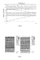
- FIG. 3 is a photonic band map of the second square-lattice slab PhC shown in some embodiments 1.
- FIG. 4 is a photonic band map of the first square-lattice slab PhC shown in some embodiments 1.
- FIG. 5 is a photonic band map of the second square-lattice slab PhC shown in embodiments 2.
- FIG. 6 is a photonic band map of the first square-lattice slab PhC shown in some embodiments 2.
- FIG. 7 is an optical field (electric field) distribution diagram of the TEOS for the normalized operating frequency (a/ ⁇ ) of 0.4057 as shown in some embodiments 3, wherein the wave is incident from top, the left-hand-side plot shows the OFF state that the wave cannot go through, and the right-hand-side plot shows the ON state that the wave may go through.
- a/ ⁇ normalized operating frequency
- FIG. 8 is an optical field (electric field) distribution diagram of the TEOS for the normalized operating frequency (a/ ⁇ ) of 0.4058 as shown in some embodiments 4, wherein the wave is incident from top, the left-hand-side plot shows the OFF state that the wave cannot go through, and the right-hand-side plot shows the ON state that the wave may go through.
- a/ ⁇ normalized operating frequency
- FIG. 9 is an optical field (electric field) distribution diagram of the TEOS for the normalized operating frequency (a/ ⁇ ) of 0.406 as shown in some embodiments 5, wherein the wave is incident from top, the left-hand-side plot shows the OFF state that the wave cannot go through, and the right-hand-side plot shows the ON state that the wave may go through.
- a/ ⁇ normalized operating frequency
- FIG. 10 is an optical field (electric field) distribution diagram of the TEOS for the normalized operating frequency (a/ ⁇ ) of 0.4267 as shown in some embodiments 6, wherein the wave is incident from top, the left-hand-side plot shows the OFF state that the wave cannot go through, and the right-hand-side plot shows the ON state that the wave may go through.
- a/ ⁇ normalized operating frequency
- FIG. 11 is an optical field (electric field) distribution diagram of the TEOS for the normalized operating frequency (a/ ⁇ ) of 0.4315 as shown in some embodiments 7, wherein the wave is incident from top, the left-hand-side plot shows the ON state that the wave cannot go through, and the right-hand-side plot shows the OFF state that the wave may go through.
- a/ ⁇ normalized operating frequency
- FIG. 12 is an optical field (electric field) distribution diagram of the TEOS for the normalized operating frequency (a/ ⁇ ) of 0.4329 as shown in some embodiments 8, wherein the wave is incident from top, the left-hand-side plot shows the OFF state that the wave cannot go through, and the right-hand-side plot shows the ON state that the wave may go through.
- a/ ⁇ normalized operating frequency
- FIG. 13 is an optical field (electric field) distribution diagram of the TEOS for the normalized operating frequency (a/ ⁇ ) of 0.44 as shown in some embodiments 9, wherein the wave is incident from top, the left-hand-side plot shows the OFF state that the wave cannot go through, and the right-hand-side plot shows the ON state that the wave may go through.
- a/ ⁇ normalized operating frequency
- FIG. 14 is an optical field (electric field) distribution diagram of the TEOS for the normalized operating frequency (a/ ⁇ ) of 0.4435 as shown in some embodiments 10, wherein the wave is incident from top, the left-hand-side plot shows the ON state that the wave cannot go through, and the right-hand-side plot shows the OFF state that the wave may go through.
- a/ ⁇ normalized operating frequency
- FIG. 15 is an optical field (electric field) distribution diagram of the TEOS for the normalized operating frequency (a/ ⁇ ) of 0.452 as shown in some embodiments 11, wherein the wave is incident from top, the left-hand-side plot shows the OFF state that the wave cannot go through, and the right-hand-side plot shows the ON state that the wave may go through.
- a/ ⁇ normalized operating frequency
- FIG. 16 is an optical field (electric field) distribution diagram of the TEOS for the normalized operating frequency (a/ ⁇ ) of 0.456 as shown in some embodiments 12, wherein the wave is incident from top, the left-hand-side plot shows the ON state that the wave cannot go through, and the right-hand-side plot shows the OFF state that the wave may go through.
- a/ ⁇ normalized operating frequency
- FIG. 17 is an optical field (electric field) distribution diagram of the TEOS for the normalized operating frequency (a/ ⁇ ) of 0.479 as shown in some embodiments 13, wherein the wave is incident from top, the left-hand-side plot shows the ON state that the wave cannot go through, and the right-hand-side plot shows the OFF state that the wave may go through.
- a/ ⁇ normalized operating frequency
- a or an as used herein, are defined as one or more than one.
- plurality as used herein, is defined as two or more than two.
- another as used herein, is defined as at least a second or more.
- a transverse electric optical switch (TEOS) with a high extinction ratio (EXR) based on slab photonic crystals (PhCs) in the present disclosure includes an upper slab photonic crystal (PhC) and a lower slab PhC connected as a whole;
- the upper slab PhC is a first square-lattice slab PhC, the unit cell of the first square-lattice slab PhC includes a high-refractive-index first rotated-square pillar 012 , the three first flat dielectric pillars 011 and a background dielectric, the three first flat dielectric pillars 011 are arranged horizontally, the three first flat dielectric pillars 011 make the upper slab PhC connected as a whole, and each of the first flat dielectric pillars 011 includes a high-refractive-index dielectric pipe and a low-refractive-index dielectric in the pipe, or 1 to 3 of a high-refractive-index flat films; as shown in FIG.
- the lower slab PhC is a second square-lattice slab PhC with a complete band gap
- the unit cell of the second square-lattice slab PhC includes a high-refractive-index second rotated-square pillar 012 , three second flat dielectric pillars 021 and a background dielectric
- the three second flat dielectric pillars 021 are arranged horizontally
- the three second flat dielectric pillars 021 make the lower slab PhC connected as a whole
- the three second flat dielectric pillars 021 are high-refractive-index dielectric pillars
- the high-refractive-index dielectric is silicon, gallium arsenide, or titanium dioxide
- the high-refractive-index dielectric is the different dielectric having a refractive index of more than 2
- the background dielectric is the low-refractive-index dielectric
- the low-refractive-index dielectric is vacuum, air, cryolite, silica, organic foam, or olive oil, and the low-refractive-
- the normalized operating frequency (a/ ⁇ ) of the TEOS with a high EXR is 0.4057 to 0.406, 0.4267 to 0.4392 or 0.44 to 0.479, wherein a is the lattice constant of the first and second square-lattice slab PhCs, A is the wavelength of incident wave, and the frequency range is either the transverse electric (TE) transmission band of the first slab PhC and the band gap of the second square-lattice slab PhC, or the second square-lattice slab PhC and the TE transmission band and TE band gap of the first square-lattice slab PhC, wherein a is the lattice constant of the first and second square-lattice slab PhCs, and A is the wavelength of incident wave.
- TE transverse electric
- a state in which the first square-lattice slab PhC is located in the optical channel (OCH) and the second square-lattice slab PhC is located outside the OCH is a first switch state of the TEOS (i.e., optically connected state); another state in which the second slab PhC is located in the OCH and the first square-lattice slab PhC is located outside the OCH, is a second switch state of the TEOS (i.e., optically disconnected state); and wherein the first slab lattice PhC is located in the OCH and the second square-lattice slab PhC is located outside the OCH, is an optically connected state; wherein the second square-
- a/ ⁇ the normalized operating frequency (a/ ⁇ ) of the TEOS being 0.4267 to 0.4329, wherein a is the lattice constant of the first and second square-lattice slab PhCs, A is the wavelength of incident wave, and the EXR is ⁇ 32 dB to ⁇ 35 dB; wherein the second square-lattice slab PhC is located in the OCH and the first square-lattice slab PhC is located outside the OCH, is an optically connected state; wherein the first square-lattice slab PhC is located in the OCH and the second square-lattice slab PhC is located outside the OCH, is an optically disconnected state.
- a/ ⁇ the normalized operating frequency (a/ ⁇ ) of the high EXR TEOS being 0.44 to 0.479, wherein a is the lattice constant of the first and second square-lattice slab PhCs, A is the wavelength of incident wave, and the EXR is ⁇ 20 dB to ⁇ 40 dB; wherein the second square-lattice slab PhC is located in the OCH and the first square-lattice slab PhC is located outside the OCH, is an optically connected state; wherein the first square-lattice slab PhC is located in the OCH and the second square-lattice slab PhC is located outside the OCH, is an optically disconnected state.
- the EXR of the TEOS is a ratio of the output optical powers of the switch in the two states.
- the first implementation of the TEOS with a high EXR based on slab PhCs of the present disclosure is the first implementation of the TEOS with a high EXR based on slab PhCs of the present disclosure.
- the TEOS with a high EXR includes an upper slab PhC and a lower slab PhC connected as a whole; as shown in FIG. 2A , the high-refractive-index first and second rotated-square pillars in the PhC are omitted in the figure, and the dashed box shows the position of the high-refractive-index first and second rotated-square pillars array;
- the upper slab PhC is a first square-lattice slab PhC, the unit cell of the first square-lattice slab PhC includes a high-refractive-index first rotated-square pillar, the three first flat dielectric pillars 011 and a background dielectric, the side length of the high-refractive-index first rotated-square pillar 011 of the first square-lattice slab PhC is 0.545a to 0.564a, wherein a is the lattice constant of the first square-lattice slab PhC, the rotated angle of the first square-lattice slab PhC is 0 to
- the three first flat dielectric pillars 011 make the upper slab PhC connected as a whole, the each of the three first flat dielectric pillars 011 includes a high-refractive-index pipe and a low-refractive-index dielectric in the pipe, the thickness of the pipe wall in each of the three first flat dielectric pillar 011 in the unit cell of the first square-lattice slab PhC is 0 to 0.009a; and the width of the low-refractive-index dielectric in the pipe is the difference between the width of the single one of the first flat dielectric pillars 011 and the thickness of the pipe wall.
- the lower slab PhC is the second square-lattice slab PhC with a complete band gap
- the unit cell of the second square-lattice slab PhC includes a high-refractive-index second rotated-square pillar, the three second flat dielectric pillars 021 and a background dielectric
- the side length of the high-refractive-index second rotated-square pillars of the second square-lattice slab PhC is 0.545a to 0.564a
- a is the lattice constant of the second square-lattice slab PhC
- the rotated angle of the second square-lattice slab PhC is 0 to 90 degrees
- the width of each of the three second flat dielectric pillars 021 in the unit cell of the second square-lattice slab PhC is 0.029a to 0.034a
- the three second flat dielectric pillars 021 are arranged horizontally, and the three second flat dielectric pillars 021 make the lower slab PhC connected as a whole, the single one of the three second
- the normalized operating frequency (a/ ⁇ ) range of the TEOS with a high EXR is 0.4057 to 0.406, and the frequency range is either the TE transmission band of the first square-lattice slab PhC and the TE band gap of the second square-lattice slab PhC, or the second square-lattice slab PhC and the TE transmission band and TE band gap of the first square-lattice slab PhC, wherein a is the lattice constant of the first and second square-lattice slab PhCs, and A is the wavelength of incident wave.
- the TEOS includes an upper slab PhC and a lower slab PhC connected as a whole; as shown in FIG. 2B , the high-refractive-index first and second rotated-square pillars are omitted in the figure, and the dashed box shows the position of the high-refractive-index first and second rotated-square pillars array;
- the upper slab PhC is a first square-lattice slab PhC, the unit cell of the first square-lattice slab PhC includes a high-refractive-index first rotated-square pillar, the three first flat dielectric pillars 013 and a background dielectric, the side length of the high-refractive-index first rotated-square pillars of the first square-lattice slab PhC is 0.545a to 0.564a, wherein a is the lattice constant of the first square-lattice slab PhC, the rotated angle of the first square-lattice slab PhC is 0 to 90 degrees, and the width of the each of the three
- the lower slab PhC is the second square-lattice slab PhC with a complete band gap
- the unit cell of the second square-lattice slab PhC includes a high-refractive-index second rotated-square pillar
- the three second flat dielectric pillars 021 and a background dielectric the three second flat dielectric pillars 021 are arranged horizontally
- the three second flat dielectric pillars 021 make the lower slab PhC connected as a whole
- the single one of the three second flat dielectric pillars 021 in the unit cell of the second square-lattice slab PhC is horizontally located at the center of the second rotated-square pillar
- two remaining of the three second flat dielectric pillars 021 are respectively parallel to the single one of the three second flat dielectric pillars 021 located horizontally at the center of the second rotated-square pillar
- the distance between the two remaining of the three second flat dielectric pillars 021 is 0.25a, wherein a is the lattice constant of the second square-l
- the three second flat dielectric pillars 021 are high-refractive-index dielectric pillars, the high-refractive-index dielectric is silicon, gallium arsenide, or titanium dioxide, and the high-refractive-index dielectric is the different dielectric having a refractive index of more than 2, and the high-refractive-index dielectric adopts a silicon material; the background dielectric is a low-refractive-index dielectric, and the low-refractive-index dielectric is vacuum, air, cryolite, silica, organic foam, or olive oil, and the low-refractive-index dielectric is the different dielectric having a refractive index of less than 1.5.
- the normalized operating frequency (a/ ⁇ ) range of the TEOS with a high EXR is 0.4267 to 0.4329, and the frequency range is either the TE transmission band of the first square-lattice slab PhC and the TE band gap of the second square-lattice slab PhC, or the second square-lattice slab PhC and the TE transmission band and TE band gap of the first square-lattice slab PhC, wherein a is the lattice constant of the first and second square-lattice slab PhCs, and A is the wavelength of incident wave.
- the third implementation of the TEOS with a high EXR based on slab PhCs of the present disclosure is the third implementation of the TEOS with a high EXR based on slab PhCs of the present disclosure.
- the TEOS includes an upper slab PhC and a lower slab PhC connected as a whole; as shown in FIG. 2C , high-refractive-index first and second rotated-square pillars in the PhC are omitted in the figure, and the dashed box shows the position of the high-refractive-index first and second rotated-square pillars array.
- the upper slab PhC is a first square-lattice slab PhC, the unit cell of the first square-lattice slab PhC includes a high-refractive-index first rotated-square pillar, and a background dielectric, the background dielectric is a low-refractive-index dielectric, and the low-refractive-index dielectric is vacuum, air, cryolite, silica, organic foam, or olive oil, and the low-refractive-index dielectric is the different dielectric having a refractive index of less than 1.5 (e.g., air).
- the lower slab PhC is a second square-lattice slab PhC with a complete band gap
- the unit cell of the second square-lattice slab PhC includes a high-refractive-index second rotated-square pillar, the three second flat dielectric pillars 021 and a background dielectric, the three second flat dielectric pillars 021 are arranged horizontally, the three second flat dielectric pillars 021 make the lower slab PhC connected as a whole;
- the single one of the three second flat dielectric pillars 021 in the unit cell of the second square-lattice slab PhC is horizontally located at the center of the second rotated-square pillar, two remaining of the three second flat dielectric pillars 021 are respectively parallel to the single one of the three second flat dielectric pillars 021 located horizontally at the center of the second rotated-square pillar, and the distance between the two remaining of the three second flat dielectric pillars 021 is 0.25a, wherein a is the lattice constant of the second square-l
- the fore three implementations all take a paper surface as the reference plane, and the upper and lower slab PhCs are connected as a whole by a frame and move vertically under the action of external forces to realize the functions of the TEOS, as shown in FIGS. 2A-2C , the high-refractive-index first and second rotated-square pillars in the PhC are omitted in the figure, and the dashed box shows the position the high-refractive-index first and second rotated-square pillars array. Because the frame itself is not on the light input and output planes, i.e., the light input and output planes are parallel to the reference plane, the propagation of light is not influenced.
- the vertical movement of the upper and lower slab PhCs serving as a whole may be realized by micromechanical, electrical or magnetic forces.
- a magnet may be embedded into the frame, a pressure linkage device is connected with the frame, the pressure may thus drive the black frame to move up and down, and the left and right sides of the frame are located in a groove guide rail to guarantee that the black frame moves vertically, linearly and reciprocally.
- FIG. 3 is a photonic band map of the second square-lattice slab PhC, the TE band gap normalization frequency (a/ ⁇ ) is 0.400 to 0.4325;
- FIG. 4 is a photonic band map of the first square-lattice slab PhC, the TE band gap normalization frequency (a/ ⁇ ) is 0.4303 to 0.5216, and it may be known by comparison that for the normalized operating frequency (a/ ⁇ ) range of 0.400 to 0.4303, this structure enables a TEOS with a high EXR.
- FIG. 5 is a photonic band map of the second square-lattice slab PhC, the TE band gap normalization frequency (a/ ⁇ ) is 0.400 to 0.4325;
- FIG. 6 is a photonic band of the first square-lattice slab PhC, the TE band gap normalization frequency (a/ ⁇ ) is 0.4303 to 0.5216, and it may be known by comparison that for the normalized operating frequency (a/ ⁇ ) range being 0.400 to 0.4303, the structure enables a TEOS with a high EXR.
- the normalized operating frequency (a/ ⁇ ) is 0.4057.
- the normalized operating frequency (a/ ⁇ ) is 0.4058.
- the normalized operating frequency (a/ ⁇ ) is 0.406.
- the normalized operating frequency (a/ ⁇ ) is 0.4267.
- the normalized operating frequency (a/ ⁇ ) is 0.4315.
- the normalized operating frequency (a/ ⁇ ) is 0.4329.
- the normalized operating frequency (a/ ⁇ ) is 0.44.
- the normalized operating frequency (a/ ⁇ ) is 0.4435.
- the normalized operating frequency (a/ ⁇ ) is 0.452.
- the normalized operating frequency (a/ ⁇ ) is 0.456.
- the normalized operating frequency (a/ ⁇ ) is 0.479.
Landscapes
- Physics & Mathematics (AREA)
- General Physics & Mathematics (AREA)
- Optics & Photonics (AREA)
- Nonlinear Science (AREA)
- Engineering & Computer Science (AREA)
- Microelectronics & Electronic Packaging (AREA)
- Optical Modulation, Optical Deflection, Nonlinear Optics, Optical Demodulation, Optical Logic Elements (AREA)
- Optical Integrated Circuits (AREA)
Applications Claiming Priority (4)
| Application Number | Priority Date | Filing Date | Title |
|---|---|---|---|
| CN201410759245.2 | 2014-12-10 | ||
| CN201410759245 | 2014-12-10 | ||
| CN201410759245.2A CN104459989B (zh) | 2014-12-10 | 2014-12-10 | 基于平板光子晶体的高消光比te光开关 |
| PCT/CN2015/097055 WO2016091195A1 (zh) | 2014-12-10 | 2015-12-10 | 基于平板光子晶体的高消光比te光开关 |
Related Parent Applications (1)
| Application Number | Title | Priority Date | Filing Date |
|---|---|---|---|
| PCT/CN2015/097055 Continuation WO2016091195A1 (zh) | 2014-12-10 | 2015-12-10 | 基于平板光子晶体的高消光比te光开关 |
Publications (2)
| Publication Number | Publication Date |
|---|---|
| US20170285440A1 US20170285440A1 (en) | 2017-10-05 |
| US10095082B2 true US10095082B2 (en) | 2018-10-09 |
Family
ID=52906304
Family Applications (1)
| Application Number | Title | Priority Date | Filing Date |
|---|---|---|---|
| US15/626,156 Expired - Fee Related US10095082B2 (en) | 2014-12-10 | 2017-06-18 | TE optical switch with high extinction ratio based on slab photonic crystals |
Country Status (3)
| Country | Link |
|---|---|
| US (1) | US10095082B2 (zh) |
| CN (1) | CN104459989B (zh) |
| WO (1) | WO2016091195A1 (zh) |
Families Citing this family (5)
| Publication number | Priority date | Publication date | Assignee | Title |
|---|---|---|---|---|
| CN104459988B (zh) * | 2014-12-10 | 2017-07-18 | 欧阳征标 | 基于平板光子晶体的高偏振度及高消光比tm光开关 |
| CN104459989B (zh) | 2014-12-10 | 2017-03-08 | 深圳市浩源光电技术有限公司 | 基于平板光子晶体的高消光比te光开关 |
| CN104375267B (zh) * | 2014-12-10 | 2017-01-11 | 欧阳征标 | 基于平板光子晶体高消光比tm光开关 |
| CN104459990B (zh) | 2014-12-10 | 2017-01-11 | 欧阳征标 | 基于平板光子晶体的高消光比偏振无关光开关 |
| CN104849806B (zh) * | 2015-05-27 | 2017-10-03 | 欧阳征标 | 基于十字连杆与旋转空心正方柱的二维正方晶格光子晶体 |
Citations (23)
| Publication number | Priority date | Publication date | Assignee | Title |
|---|---|---|---|---|
| WO2003014010A1 (en) | 2001-08-08 | 2003-02-20 | Jsr Corporation | Three-dimensional opto-electronic micro-system |
| US20040001683A1 (en) * | 2002-06-27 | 2004-01-01 | The Board Of Trustees Of The Leland Stanford Junior University | Creating large bandwidth line defects by embedding dielectric waveguides into photonic crystal slabs |
| US6795621B2 (en) * | 2001-06-07 | 2004-09-21 | Nec Corporation | Waveguide comprising a connection of a photonic-crystal line-defect-waveguide to a total reflection confinement waveguide |
| US20040247009A1 (en) * | 2001-07-05 | 2004-12-09 | Susumu Noda | Two-dimensional photonic crystal surface-emitting laser |
| US6853760B2 (en) * | 2000-01-24 | 2005-02-08 | Minolta Co., Ltd. | Optical functional device and optical integrated device |
| US6873777B2 (en) * | 2003-03-10 | 2005-03-29 | Japan Aviation Electronics Industry Limited | Two-dimensional photonic crystal device |
| US20050100296A1 (en) * | 2002-07-01 | 2005-05-12 | Mesophotonics Limited | Optical device |
| US7269310B2 (en) * | 2005-03-08 | 2007-09-11 | Japan Aviation Electronics Industry Limited | Optical connector, optical coupling method and optical element |
| US7373059B2 (en) * | 2006-09-22 | 2008-05-13 | Hewlett-Packard Development Company, L.P. | Compact, single chip-based, entangled polarization-state photon sources and methods for generating photons in entangled polarization states |
| US7421179B1 (en) * | 2006-09-29 | 2008-09-02 | Wei Jiang | Apparatus and method for switching, modulation and dynamic control of light transmission using photonic crystals |
| US7440658B2 (en) * | 2004-03-03 | 2008-10-21 | Japan Science And Technology Agency | Photonic crystal coupling defect waveguide |
| US7529437B2 (en) * | 2006-07-27 | 2009-05-05 | Hewlett-Packard Development Company, L.P. | Scalable and defect-tolerant quantum-dot-based quantum computer architectures and methods for fabricating quantum dots in quantum computer architectures |
| CN101571657A (zh) | 2009-06-10 | 2009-11-04 | 南京邮电大学 | 一种光子晶体全光开关 |
| US7783139B2 (en) * | 2005-03-18 | 2010-08-24 | Kyoto University | Polarized light mode converter |
| US7831124B2 (en) * | 2006-09-21 | 2010-11-09 | The Furukawa Electric Co., Ltd. | Photonic crystal optical device |
| US20110002581A1 (en) * | 2008-02-07 | 2011-01-06 | Masatoshi Tokushima | Optical switch and method of manufacturing the same |
| US8571373B2 (en) | 2011-05-23 | 2013-10-29 | Xiaolong Wang | Photonic crystal band-shifting device for dynamic control of light transmission |
| US8617471B2 (en) * | 2010-08-23 | 2013-12-31 | Omega Optics, Inc. | Fabrication tolerant design for the chip-integrated spectroscopic identification of solids, liquids, and gases |
| CN104375267A (zh) | 2014-12-10 | 2015-02-25 | 欧阳征标 | 基于平板光子晶体高消光比tm光开关 |
| CN104459988A (zh) | 2014-12-10 | 2015-03-25 | 欧阳征标 | 基于平板光子晶体的高偏振度及高消光比tm光开关 |
| CN104459991A (zh) | 2014-12-10 | 2015-03-25 | 欧阳征标 | 基于平板光子晶体的高偏振度及高消光比te光开关 |
| CN104459989A (zh) | 2014-12-10 | 2015-03-25 | 欧阳征标 | 基于平板光子晶体的高消光比te光开关 |
| CN104459990A (zh) | 2014-12-10 | 2015-03-25 | 欧阳征标 | 基于平板光子晶体的高消光比偏振无关光开关 |
Family Cites Families (5)
| Publication number | Priority date | Publication date | Assignee | Title |
|---|---|---|---|---|
| JP2003215646A (ja) * | 2002-01-21 | 2003-07-30 | Matsushita Electric Works Ltd | 光スイッチ |
| CN102650714B (zh) * | 2012-01-13 | 2015-04-08 | 深圳大学 | 光子晶体波导t形偏振分束器 |
| CN103901536B (zh) * | 2014-04-11 | 2016-08-17 | 深圳大学 | 一种圆环杆与平板连杆的二维正方晶格光子晶体 |
| CN104155718B (zh) * | 2014-07-28 | 2017-07-04 | 欧阳征标 | 基于高折射率内圆外方空心柱的正方晶格光子晶体 |
| CN104101949B (zh) * | 2014-07-28 | 2017-01-25 | 欧阳征标 | 基于十字连杆柱和圆柱的大绝对禁带正方晶格光子晶体 |
-
2014
- 2014-12-10 CN CN201410759245.2A patent/CN104459989B/zh active Active
-
2015
- 2015-12-10 WO PCT/CN2015/097055 patent/WO2016091195A1/zh active Application Filing
-
2017
- 2017-06-18 US US15/626,156 patent/US10095082B2/en not_active Expired - Fee Related
Patent Citations (24)
| Publication number | Priority date | Publication date | Assignee | Title |
|---|---|---|---|---|
| US6853760B2 (en) * | 2000-01-24 | 2005-02-08 | Minolta Co., Ltd. | Optical functional device and optical integrated device |
| US6795621B2 (en) * | 2001-06-07 | 2004-09-21 | Nec Corporation | Waveguide comprising a connection of a photonic-crystal line-defect-waveguide to a total reflection confinement waveguide |
| US20040247009A1 (en) * | 2001-07-05 | 2004-12-09 | Susumu Noda | Two-dimensional photonic crystal surface-emitting laser |
| WO2003014010A1 (en) | 2001-08-08 | 2003-02-20 | Jsr Corporation | Three-dimensional opto-electronic micro-system |
| US20040001683A1 (en) * | 2002-06-27 | 2004-01-01 | The Board Of Trustees Of The Leland Stanford Junior University | Creating large bandwidth line defects by embedding dielectric waveguides into photonic crystal slabs |
| US20050100296A1 (en) * | 2002-07-01 | 2005-05-12 | Mesophotonics Limited | Optical device |
| US6873777B2 (en) * | 2003-03-10 | 2005-03-29 | Japan Aviation Electronics Industry Limited | Two-dimensional photonic crystal device |
| US7440658B2 (en) * | 2004-03-03 | 2008-10-21 | Japan Science And Technology Agency | Photonic crystal coupling defect waveguide |
| US7269310B2 (en) * | 2005-03-08 | 2007-09-11 | Japan Aviation Electronics Industry Limited | Optical connector, optical coupling method and optical element |
| US7783139B2 (en) * | 2005-03-18 | 2010-08-24 | Kyoto University | Polarized light mode converter |
| US7529437B2 (en) * | 2006-07-27 | 2009-05-05 | Hewlett-Packard Development Company, L.P. | Scalable and defect-tolerant quantum-dot-based quantum computer architectures and methods for fabricating quantum dots in quantum computer architectures |
| US7831124B2 (en) * | 2006-09-21 | 2010-11-09 | The Furukawa Electric Co., Ltd. | Photonic crystal optical device |
| US7373059B2 (en) * | 2006-09-22 | 2008-05-13 | Hewlett-Packard Development Company, L.P. | Compact, single chip-based, entangled polarization-state photon sources and methods for generating photons in entangled polarization states |
| US7421179B1 (en) * | 2006-09-29 | 2008-09-02 | Wei Jiang | Apparatus and method for switching, modulation and dynamic control of light transmission using photonic crystals |
| US20110002581A1 (en) * | 2008-02-07 | 2011-01-06 | Masatoshi Tokushima | Optical switch and method of manufacturing the same |
| CN101571657A (zh) | 2009-06-10 | 2009-11-04 | 南京邮电大学 | 一种光子晶体全光开关 |
| US8617471B2 (en) * | 2010-08-23 | 2013-12-31 | Omega Optics, Inc. | Fabrication tolerant design for the chip-integrated spectroscopic identification of solids, liquids, and gases |
| US8571373B2 (en) | 2011-05-23 | 2013-10-29 | Xiaolong Wang | Photonic crystal band-shifting device for dynamic control of light transmission |
| CN104375267A (zh) | 2014-12-10 | 2015-02-25 | 欧阳征标 | 基于平板光子晶体高消光比tm光开关 |
| CN104459988A (zh) | 2014-12-10 | 2015-03-25 | 欧阳征标 | 基于平板光子晶体的高偏振度及高消光比tm光开关 |
| CN104459991A (zh) | 2014-12-10 | 2015-03-25 | 欧阳征标 | 基于平板光子晶体的高偏振度及高消光比te光开关 |
| CN104459989A (zh) | 2014-12-10 | 2015-03-25 | 欧阳征标 | 基于平板光子晶体的高消光比te光开关 |
| CN104459990A (zh) | 2014-12-10 | 2015-03-25 | 欧阳征标 | 基于平板光子晶体的高消光比偏振无关光开关 |
| WO2016091195A1 (zh) | 2014-12-10 | 2016-06-16 | 深圳大学 | 基于平板光子晶体的高消光比te光开关 |
Non-Patent Citations (1)
| Title |
|---|
| Ming-Chang M. Lee, Dooyoung Hah, Erwin K Lau, Hiroshi Toshiyoshi and Ming Wu, "MEMS-Actuated Photonic Crystal Switches", IEEE Photonics Technology Letters, Jan. 15, 2006, pp. 358-360, vol. 18, No. 2. |
Also Published As
| Publication number | Publication date |
|---|---|
| CN104459989B (zh) | 2017-03-08 |
| WO2016091195A1 (zh) | 2016-06-16 |
| US20170285440A1 (en) | 2017-10-05 |
| CN104459989A (zh) | 2015-03-25 |
Similar Documents
| Publication | Publication Date | Title |
|---|---|---|
| US10095082B2 (en) | TE optical switch with high extinction ratio based on slab photonic crystals | |
| US9880444B2 (en) | TM optical switch with high extinction ratio based on slab photonic crystals | |
| US9971227B2 (en) | TM optical switch based on slab photonic crystals with high degree of polarization and large extinction ratio | |
| US9904010B2 (en) | Polarization independent optical switch with high extinction ratio based on slab photonic crystals | |
| US9885939B2 (en) | TE optical switch based on slab photonic crystals with high degree of polarization and large extinction ratio | |
| US20170242156A1 (en) | Two-dimensional square-lattice photonic crystal with cross-shaped connecting rods and rotated square rods | |
| CN110501821B (zh) | 一种基于pt对称结构与磁光子晶体的可调谐单向交叉波导分配器 | |
| Suzuki et al. | Ultralow-crosstalk and broadband multi-port optical switch using SiN/Si double-layer platform | |
| CN101995604B (zh) | 一种基于斜体蜂巢结构的二维光子晶体慢光波导实现方法 | |
| CN114185116B (zh) | 一种能够实现拓扑边界态和/或零维角态的拓扑光通信器件 | |
| US20170146737A1 (en) | Right-angle waveguide based on circular-hole-type square-lattice photonic crystal and dual compensation scattering cylinders with low refractive index | |
| US20170108644A1 (en) | Right-angle waveguide based on square-cylinder-type square-lattice photonic crystal and dual compensation scattering cylinders with high refractive index | |
| CN210428000U (zh) | 一种基于磁光介质与pt对称结构的多通道信号选择器 | |
| CN110646958B (zh) | 一种基于磁光介质与pt对称结构的多通道信号选择器及其使用方法 | |
| CN101923226A (zh) | 基于自准直效应的光子晶体偏振分束器结构 | |
| Vertchenko et al. | Low Index Asymmetric Bound States in the Continuum for Low Loss Integrated Photonics | |
| US20170108647A1 (en) | Right-angle waveguide based on square-hole-type square-lattice photonic crystal and dual compensation scattering cylinders with low refractive index | |
| US9709736B2 (en) | Right-angle waveguide based on square-cylinder-type square-lattice photonic crystal and single compensation scattering cylinder with high refractive index | |
| Campione et al. | Compact Silicon Photonic Phase Modulators based on Epsilon-Near_Zero Materials. | |
| CN114839719B (zh) | 一种基于拓扑旋磁光子晶体单向大面积t-型波导分束器 | |
| CN102789023A (zh) | 光子晶体分束器 | |
| Wu et al. | New design of the polarization beam splitter based on photonic crystals | |
| CN117031795A (zh) | 一种单向可调磁光光子晶体慢光延时器件的构建方法 | |
| US20170108646A1 (en) | Right-angle waveguide based on circular-cylinder-type square-lattice photonic crystal and dual compensation scattering cylinders with high refractive index | |
| Liu et al. | Slow Light Properties of 2D Photonic Crystal Waveguide for Optical Storage in Optical Computers |
Legal Events
| Date | Code | Title | Description |
|---|---|---|---|
| AS | Assignment |
Owner name: OUYANG, ZHENGBIAO, CHINA Free format text: ASSIGNMENT OF ASSIGNORS INTEREST;ASSIGNORS:OUYANG, ZHENGBIAO;WEN, GUOHUA;REEL/FRAME:042741/0206 Effective date: 20170612 |
|
| STCF | Information on status: patent grant |
Free format text: PATENTED CASE |
|
| FEPP | Fee payment procedure |
Free format text: MAINTENANCE FEE REMINDER MAILED (ORIGINAL EVENT CODE: REM.); ENTITY STATUS OF PATENT OWNER: SMALL ENTITY |
|
| LAPS | Lapse for failure to pay maintenance fees |
Free format text: PATENT EXPIRED FOR FAILURE TO PAY MAINTENANCE FEES (ORIGINAL EVENT CODE: EXP.); ENTITY STATUS OF PATENT OWNER: SMALL ENTITY |
|
| STCH | Information on status: patent discontinuation |
Free format text: PATENT EXPIRED DUE TO NONPAYMENT OF MAINTENANCE FEES UNDER 37 CFR 1.362 |
|
| FP | Lapsed due to failure to pay maintenance fee |
Effective date: 20221009 |