US10032863B2 - Isolated semiconductor layer in bulk wafer by localized silicon epitaxial seed formation - Google Patents
Isolated semiconductor layer in bulk wafer by localized silicon epitaxial seed formation Download PDFInfo
- Publication number
- US10032863B2 US10032863B2 US15/090,000 US201615090000A US10032863B2 US 10032863 B2 US10032863 B2 US 10032863B2 US 201615090000 A US201615090000 A US 201615090000A US 10032863 B2 US10032863 B2 US 10032863B2
- Authority
- US
- United States
- Prior art keywords
- layer
- integrated circuit
- silicon
- dielectric layer
- epitaxial
- Prior art date
- Legal status (The legal status is an assumption and is not a legal conclusion. Google has not performed a legal analysis and makes no representation as to the accuracy of the status listed.)
- Active
Links
Images


Classifications
-
- H01L29/0653—
-
- H—ELECTRICITY
- H10—SEMICONDUCTOR DEVICES; ELECTRIC SOLID-STATE DEVICES NOT OTHERWISE PROVIDED FOR
- H10D—INORGANIC ELECTRIC SEMICONDUCTOR DEVICES
- H10D62/00—Semiconductor bodies, or regions thereof, of devices having potential barriers
- H10D62/10—Shapes, relative sizes or dispositions of the regions of the semiconductor bodies; Shapes of the semiconductor bodies
- H10D62/113—Isolations within a component, i.e. internal isolations
- H10D62/115—Dielectric isolations, e.g. air gaps
- H10D62/116—Dielectric isolations, e.g. air gaps adjoining the input or output regions of field-effect devices, e.g. adjoining source or drain regions
-
- H01L21/02164—
-
- H01L21/0217—
-
- H01L21/0223—
-
- H01L21/02636—
-
- H01L21/02645—
-
- H01L21/02667—
-
- H01L21/02675—
-
- H01L21/02686—
-
- H01L21/30625—
-
- H01L21/3065—
-
- H01L21/31055—
-
- H01L21/76224—
-
- H01L21/76248—
-
- H01L21/76278—
-
- H01L21/76283—
-
- H01L21/84—
-
- H01L27/12—
-
- H01L27/1203—
-
- H01L29/04—
-
- H01L29/0649—
-
- H01L29/7851—
-
- H—ELECTRICITY
- H10—SEMICONDUCTOR DEVICES; ELECTRIC SOLID-STATE DEVICES NOT OTHERWISE PROVIDED FOR
- H10D—INORGANIC ELECTRIC SEMICONDUCTOR DEVICES
- H10D30/00—Field-effect transistors [FET]
- H10D30/60—Insulated-gate field-effect transistors [IGFET]
- H10D30/62—Fin field-effect transistors [FinFET]
- H10D30/6211—Fin field-effect transistors [FinFET] having fin-shaped semiconductor bodies integral with the bulk semiconductor substrates
-
- H—ELECTRICITY
- H10—SEMICONDUCTOR DEVICES; ELECTRIC SOLID-STATE DEVICES NOT OTHERWISE PROVIDED FOR
- H10D—INORGANIC ELECTRIC SEMICONDUCTOR DEVICES
- H10D62/00—Semiconductor bodies, or regions thereof, of devices having potential barriers
- H10D62/10—Shapes, relative sizes or dispositions of the regions of the semiconductor bodies; Shapes of the semiconductor bodies
- H10D62/113—Isolations within a component, i.e. internal isolations
- H10D62/115—Dielectric isolations, e.g. air gaps
-
- H—ELECTRICITY
- H10—SEMICONDUCTOR DEVICES; ELECTRIC SOLID-STATE DEVICES NOT OTHERWISE PROVIDED FOR
- H10D—INORGANIC ELECTRIC SEMICONDUCTOR DEVICES
- H10D62/00—Semiconductor bodies, or regions thereof, of devices having potential barriers
- H10D62/40—Crystalline structures
-
- H—ELECTRICITY
- H10—SEMICONDUCTOR DEVICES; ELECTRIC SOLID-STATE DEVICES NOT OTHERWISE PROVIDED FOR
- H10D—INORGANIC ELECTRIC SEMICONDUCTOR DEVICES
- H10D86/00—Integrated devices formed in or on insulating or conducting substrates, e.g. formed in silicon-on-insulator [SOI] substrates or on stainless steel or glass substrates
- H10D86/01—Manufacture or treatment
-
- H—ELECTRICITY
- H10—SEMICONDUCTOR DEVICES; ELECTRIC SOLID-STATE DEVICES NOT OTHERWISE PROVIDED FOR
- H10D—INORGANIC ELECTRIC SEMICONDUCTOR DEVICES
- H10D86/00—Integrated devices formed in or on insulating or conducting substrates, e.g. formed in silicon-on-insulator [SOI] substrates or on stainless steel or glass substrates
- H10D86/201—Integrated devices formed in or on insulating or conducting substrates, e.g. formed in silicon-on-insulator [SOI] substrates or on stainless steel or glass substrates the substrates comprising an insulating layer on a semiconductor body, e.g. SOI
-
- H—ELECTRICITY
- H10—SEMICONDUCTOR DEVICES; ELECTRIC SOLID-STATE DEVICES NOT OTHERWISE PROVIDED FOR
- H10P—GENERIC PROCESSES OR APPARATUS FOR THE MANUFACTURE OR TREATMENT OF DEVICES COVERED BY CLASS H10
- H10P14/00—Formation of materials, e.g. in the shape of layers or pillars
- H10P14/20—Formation of materials, e.g. in the shape of layers or pillars of semiconductor materials
- H10P14/27—Formation of materials, e.g. in the shape of layers or pillars of semiconductor materials using selective deposition, e.g. simultaneous growth of monocrystalline and non-monocrystalline semiconductor materials
- H10P14/271—Formation of materials, e.g. in the shape of layers or pillars of semiconductor materials using selective deposition, e.g. simultaneous growth of monocrystalline and non-monocrystalline semiconductor materials characterised by the preparation of substrate for selective deposition
- H10P14/274—Formation of materials, e.g. in the shape of layers or pillars of semiconductor materials using selective deposition, e.g. simultaneous growth of monocrystalline and non-monocrystalline semiconductor materials characterised by the preparation of substrate for selective deposition using seed materials
-
- H—ELECTRICITY
- H10—SEMICONDUCTOR DEVICES; ELECTRIC SOLID-STATE DEVICES NOT OTHERWISE PROVIDED FOR
- H10P—GENERIC PROCESSES OR APPARATUS FOR THE MANUFACTURE OR TREATMENT OF DEVICES COVERED BY CLASS H10
- H10P14/00—Formation of materials, e.g. in the shape of layers or pillars
- H10P14/20—Formation of materials, e.g. in the shape of layers or pillars of semiconductor materials
- H10P14/38—Formation of materials, e.g. in the shape of layers or pillars of semiconductor materials characterised by treatments done after the formation of the materials
- H10P14/3802—Crystallisation or recrystallisation of non-monocrystalline semiconductor materials, e.g. regrowth
- H10P14/3808—Crystallisation or recrystallisation of non-monocrystalline semiconductor materials, e.g. regrowth using laser beams
- H10P14/3816—Pulsed laser beam
-
- H—ELECTRICITY
- H10—SEMICONDUCTOR DEVICES; ELECTRIC SOLID-STATE DEVICES NOT OTHERWISE PROVIDED FOR
- H10P—GENERIC PROCESSES OR APPARATUS FOR THE MANUFACTURE OR TREATMENT OF DEVICES COVERED BY CLASS H10
- H10P14/00—Formation of materials, e.g. in the shape of layers or pillars
- H10P14/60—Formation of materials, e.g. in the shape of layers or pillars of insulating materials
- H10P14/63—Formation of materials, e.g. in the shape of layers or pillars of insulating materials characterised by the formation processes
- H10P14/6302—Non-deposition formation processes
- H10P14/6304—Formation by oxidation, e.g. oxidation of the substrate
-
- H—ELECTRICITY
- H10—SEMICONDUCTOR DEVICES; ELECTRIC SOLID-STATE DEVICES NOT OTHERWISE PROVIDED FOR
- H10P—GENERIC PROCESSES OR APPARATUS FOR THE MANUFACTURE OR TREATMENT OF DEVICES COVERED BY CLASS H10
- H10P14/00—Formation of materials, e.g. in the shape of layers or pillars
- H10P14/60—Formation of materials, e.g. in the shape of layers or pillars of insulating materials
- H10P14/69—Inorganic materials
- H10P14/692—Inorganic materials composed of oxides, glassy oxides or oxide-based glasses
- H10P14/6921—Inorganic materials composed of oxides, glassy oxides or oxide-based glasses containing silicon
- H10P14/69215—Inorganic materials composed of oxides, glassy oxides or oxide-based glasses containing silicon the material being a silicon oxide, e.g. SiO2
-
- H—ELECTRICITY
- H10—SEMICONDUCTOR DEVICES; ELECTRIC SOLID-STATE DEVICES NOT OTHERWISE PROVIDED FOR
- H10P—GENERIC PROCESSES OR APPARATUS FOR THE MANUFACTURE OR TREATMENT OF DEVICES COVERED BY CLASS H10
- H10P14/00—Formation of materials, e.g. in the shape of layers or pillars
- H10P14/60—Formation of materials, e.g. in the shape of layers or pillars of insulating materials
- H10P14/69—Inorganic materials
- H10P14/694—Inorganic materials composed of nitrides
- H10P14/6943—Inorganic materials composed of nitrides containing silicon
- H10P14/69433—Inorganic materials composed of nitrides containing silicon the material being a silicon nitride not containing oxygen, e.g. SixNy or SixByNz
-
- H—ELECTRICITY
- H10—SEMICONDUCTOR DEVICES; ELECTRIC SOLID-STATE DEVICES NOT OTHERWISE PROVIDED FOR
- H10P—GENERIC PROCESSES OR APPARATUS FOR THE MANUFACTURE OR TREATMENT OF DEVICES COVERED BY CLASS H10
- H10P50/00—Etching of wafers, substrates or parts of devices
- H10P50/20—Dry etching; Plasma etching; Reactive-ion etching
- H10P50/24—Dry etching; Plasma etching; Reactive-ion etching of semiconductor materials
- H10P50/242—Dry etching; Plasma etching; Reactive-ion etching of semiconductor materials of Group IV materials
-
- H—ELECTRICITY
- H10—SEMICONDUCTOR DEVICES; ELECTRIC SOLID-STATE DEVICES NOT OTHERWISE PROVIDED FOR
- H10P—GENERIC PROCESSES OR APPARATUS FOR THE MANUFACTURE OR TREATMENT OF DEVICES COVERED BY CLASS H10
- H10P52/00—Grinding, lapping or polishing of wafers, substrates or parts of devices
- H10P52/40—Chemomechanical polishing [CMP]
- H10P52/402—Chemomechanical polishing [CMP] of semiconductor materials
-
- H—ELECTRICITY
- H10—SEMICONDUCTOR DEVICES; ELECTRIC SOLID-STATE DEVICES NOT OTHERWISE PROVIDED FOR
- H10P—GENERIC PROCESSES OR APPARATUS FOR THE MANUFACTURE OR TREATMENT OF DEVICES COVERED BY CLASS H10
- H10P90/00—Preparation of wafers not covered by a single main group of this subclass, e.g. wafer reinforcement
- H10P90/19—Preparing inhomogeneous wafers
- H10P90/1904—Preparing vertically inhomogeneous wafers
- H10P90/1906—Preparing SOI wafers
- H10P90/1912—Preparing SOI wafers using selective deposition, e.g. epitaxial lateral overgrowth [ELO] or selective deposition of single crystal silicon
-
- H—ELECTRICITY
- H10—SEMICONDUCTOR DEVICES; ELECTRIC SOLID-STATE DEVICES NOT OTHERWISE PROVIDED FOR
- H10P—GENERIC PROCESSES OR APPARATUS FOR THE MANUFACTURE OR TREATMENT OF DEVICES COVERED BY CLASS H10
- H10P95/00—Generic processes or apparatus for manufacture or treatments not covered by the other groups of this subclass
- H10P95/06—Planarisation of inorganic insulating materials
- H10P95/062—Planarisation of inorganic insulating materials involving a dielectric removal step
- H10P95/064—Planarisation of inorganic insulating materials involving a dielectric removal step the removal being chemical etching
-
- H—ELECTRICITY
- H10—SEMICONDUCTOR DEVICES; ELECTRIC SOLID-STATE DEVICES NOT OTHERWISE PROVIDED FOR
- H10W—GENERIC PACKAGES, INTERCONNECTIONS, CONNECTORS OR OTHER CONSTRUCTIONAL DETAILS OF DEVICES COVERED BY CLASS H10
- H10W10/00—Isolation regions in semiconductor bodies between components of integrated devices
- H10W10/01—Manufacture or treatment
- H10W10/011—Manufacture or treatment of isolation regions comprising dielectric materials
- H10W10/014—Manufacture or treatment of isolation regions comprising dielectric materials using trench refilling with dielectric materials, e.g. shallow trench isolations
-
- H—ELECTRICITY
- H10—SEMICONDUCTOR DEVICES; ELECTRIC SOLID-STATE DEVICES NOT OTHERWISE PROVIDED FOR
- H10W—GENERIC PACKAGES, INTERCONNECTIONS, CONNECTORS OR OTHER CONSTRUCTIONAL DETAILS OF DEVICES COVERED BY CLASS H10
- H10W10/00—Isolation regions in semiconductor bodies between components of integrated devices
- H10W10/01—Manufacture or treatment
- H10W10/061—Manufacture or treatment using SOI processes together with lateral isolation, e.g. combinations of SOI and shallow trench isolations
-
- H—ELECTRICITY
- H10—SEMICONDUCTOR DEVICES; ELECTRIC SOLID-STATE DEVICES NOT OTHERWISE PROVIDED FOR
- H10W—GENERIC PACKAGES, INTERCONNECTIONS, CONNECTORS OR OTHER CONSTRUCTIONAL DETAILS OF DEVICES COVERED BY CLASS H10
- H10W10/00—Isolation regions in semiconductor bodies between components of integrated devices
- H10W10/10—Isolation regions comprising dielectric materials
- H10W10/17—Isolation regions comprising dielectric materials formed using trench refilling with dielectric materials, e.g. shallow trench isolations
-
- H—ELECTRICITY
- H10—SEMICONDUCTOR DEVICES; ELECTRIC SOLID-STATE DEVICES NOT OTHERWISE PROVIDED FOR
- H10W—GENERIC PACKAGES, INTERCONNECTIONS, CONNECTORS OR OTHER CONSTRUCTIONAL DETAILS OF DEVICES COVERED BY CLASS H10
- H10W10/00—Isolation regions in semiconductor bodies between components of integrated devices
- H10W10/10—Isolation regions comprising dielectric materials
- H10W10/181—Semiconductor-on-insulator [SOI] isolation regions, e.g. buried oxide regions of SOI wafers
-
- H01L21/02255—
-
- H01L21/02532—
-
- H01L21/0262—
-
- H—ELECTRICITY
- H10—SEMICONDUCTOR DEVICES; ELECTRIC SOLID-STATE DEVICES NOT OTHERWISE PROVIDED FOR
- H10P—GENERIC PROCESSES OR APPARATUS FOR THE MANUFACTURE OR TREATMENT OF DEVICES COVERED BY CLASS H10
- H10P14/00—Formation of materials, e.g. in the shape of layers or pillars
- H10P14/20—Formation of materials, e.g. in the shape of layers or pillars of semiconductor materials
- H10P14/24—Formation of materials, e.g. in the shape of layers or pillars of semiconductor materials using chemical vapour deposition [CVD]
-
- H—ELECTRICITY
- H10—SEMICONDUCTOR DEVICES; ELECTRIC SOLID-STATE DEVICES NOT OTHERWISE PROVIDED FOR
- H10P—GENERIC PROCESSES OR APPARATUS FOR THE MANUFACTURE OR TREATMENT OF DEVICES COVERED BY CLASS H10
- H10P14/00—Formation of materials, e.g. in the shape of layers or pillars
- H10P14/20—Formation of materials, e.g. in the shape of layers or pillars of semiconductor materials
- H10P14/34—Deposited materials, e.g. layers
- H10P14/3402—Deposited materials, e.g. layers characterised by the chemical composition
- H10P14/3404—Deposited materials, e.g. layers characterised by the chemical composition being Group IVA materials
- H10P14/3411—Silicon, silicon germanium or germanium
-
- H—ELECTRICITY
- H10—SEMICONDUCTOR DEVICES; ELECTRIC SOLID-STATE DEVICES NOT OTHERWISE PROVIDED FOR
- H10P—GENERIC PROCESSES OR APPARATUS FOR THE MANUFACTURE OR TREATMENT OF DEVICES COVERED BY CLASS H10
- H10P14/00—Formation of materials, e.g. in the shape of layers or pillars
- H10P14/60—Formation of materials, e.g. in the shape of layers or pillars of insulating materials
- H10P14/63—Formation of materials, e.g. in the shape of layers or pillars of insulating materials characterised by the formation processes
- H10P14/6302—Non-deposition formation processes
- H10P14/6322—Formation by thermal treatments
-
- H—ELECTRICITY
- H10—SEMICONDUCTOR DEVICES; ELECTRIC SOLID-STATE DEVICES NOT OTHERWISE PROVIDED FOR
- H10W—GENERIC PACKAGES, INTERCONNECTIONS, CONNECTORS OR OTHER CONSTRUCTIONAL DETAILS OF DEVICES COVERED BY CLASS H10
- H10W10/00—Isolation regions in semiconductor bodies between components of integrated devices
- H10W10/01—Manufacture or treatment
- H10W10/021—Manufacture or treatment of air gaps
-
- H—ELECTRICITY
- H10—SEMICONDUCTOR DEVICES; ELECTRIC SOLID-STATE DEVICES NOT OTHERWISE PROVIDED FOR
- H10W—GENERIC PACKAGES, INTERCONNECTIONS, CONNECTORS OR OTHER CONSTRUCTIONAL DETAILS OF DEVICES COVERED BY CLASS H10
- H10W10/00—Isolation regions in semiconductor bodies between components of integrated devices
- H10W10/20—Air gaps
Definitions
- This invention relates to the field of integrated circuits. More particularly, this invention relates to isolated semiconductor layers in integrated circuits.
- An integrated circuit with some circuits or components in dielectrically isolated silicon may be formed on a silicon-on-insulator (SOI) wafer.
- SOI wafers are more expensive than bulk and epitaxial wafers, undesirably increasing the cost of the integrated circuit.
- the circuits or components may be formed over buried layers of silicon dioxide; methods to form the buried silicon dioxide layers such as implanting oxygen have been problematic with respect to providing desired lateral and vertical dimension control of the buried oxide layer, and undesirably increase stress on the wafer, leading to problems during photolithographic operations. Forming thin layers of device quality silicon over buried oxide layers has also been problematic.
- An integrated circuit may be formed by forming an isolation recess in a single-crystal silicon-based substrate and filling the isolation recess with isolation dielectric material to form a buried isolation layer with a top surface lower than a top surface of the adjacent substrate. Exposed lateral surfaces of the substrate at the buried isolation layer are covered with a dielectric sidewall.
- a seed trench is formed through the buried isolation layer to expose the substrate.
- a single-crystal silicon-based seed layer is formed through the seed trench, extending above the top surface of the buried isolation layer.
- a silicon-based non-crystalline layer is formed over the substrate and buried isolation layer, contacting the seed layer.
- a cap layer is formed over the non-crystalline layer.
- a radiant-induced recrystallization process heats the non-crystalline layer over the buried isolation layer and converts it to a single-crystal layer aligned with the seed layer.
- the cap layer is removed and the non-crystalline layer is removed from over the substrate, leaving an isolated semiconductor layer over the buried isolation layer.
- FIG. 1A through FIG. 1S are cross sections of an example integrated circuit, depicted in successive stages of fabrication.
- FIG. 2A through FIG. 2G are cross sections of the integrated circuit of FIG. 1A through FIG. 1S , depicting an alternate method for forming the single-crystalline region and the non-crystalline region, and for the subsequent radiant-induced recrystallization process.
- An integrated circuit may be formed by forming an isolation recess in a single-crystal silicon-based substrate and filling the isolation recess with isolation dielectric material to form a buried isolation layer with a top surface lower than a top surface of the adjacent substrate. Exposed lateral surfaces of the substrate at the buried isolation layer are covered with a dielectric sidewall.
- a seed trench is formed through the buried isolation layer to expose the substrate.
- a single-crystal silicon-based seed layer is formed through the seed trench, extending above the top surface of the buried isolation layer.
- a silicon-based non-crystalline layer is formed over the substrate and buried isolation layer, contacting the seed layer.
- a cap layer is formed over the non-crystalline layer.
- a radiant-induced recrystallization process heats the non-crystalline layer over the buried isolation layer and converts it to a single-crystal layer aligned with the seed layer.
- the cap layer is removed and the non-crystalline layer is removed from over the substrate, leaving an isolated semiconductor layer over the buried isolation layer.
- FIG. 1A through FIG. 1S are cross sections of an example integrated circuit, depicted in successive stages of fabrication.
- the integrated circuit 100 is formed on a substrate 102 of a silicon-based single-crystal semiconductor material.
- the substrate 102 may be a bulk silicon wafer or a silicon wafer with an epitaxial layer, or other substrate 102 suitable for formation of the integrated circuit 100 .
- a blocking layer 104 is formed over a top surface 106 of the substrate 102 to provide an etch mask for a subsequent trench etch and to block epitaxial growth in a subsequent epitaxy process.
- the blocking layer 104 may include a layer of silicon dioxide 108 5 nanometers to 20 nanometers thick, formed by thermal oxidation at the top surface 106 , and a layer of silicon nitride 110 50 nanometers to 150 nanometers thick formed by a low pressure chemical vapor deposition (LPCVD) process on the layer of silicon dioxide 108 .
- LPCVD low pressure chemical vapor deposition
- Other structures and compositions of the blocking layer 104 are within the scope of the instant example.
- An isolation mask 112 is formed over the blocking layer 104 so as to expose an area for an isolated semiconductor layer 114 and cover the adjacent blocking layer 104 .
- the area for the isolated semiconductor layer 114 may be, for example, 2 microns to 200 microns wide.
- the isolation mask 112 may include photoresist formed by a photolithographic process, and may include an anti-reflection layer and or hard mask material such as silicon carbide or amorphous carbon.
- the isolation mask 112 may possibly expose other areas of the integrated circuit 100 for field oxide as part of a shallow trench isolation process.
- an isolation etch process 116 removes the blocking layer 104 from the area for the isolated semiconductor layer 114 and then removes semiconductor material from the substrate 102 to form an isolation recess 118 .
- the isolation recess 118 may be, for example, 250 nanometers to 1000 nanometers deep in the substrate 102 .
- the isolation etch process 116 may be a reactive ion etch (RIE) process, as depicted schematically in FIG. 1B .
- the isolation etch process 116 may be a timed etch to provide a desired depth of the isolation recess 118 .
- the isolation mask 112 is removed; a portion of the isolation mask 112 may be removed during the isolation etch process 116 and a remaining portion may be removed after the isolation etch process 116 is completed, for example by an ash process followed by a wet clean process.
- isolation dielectric material 120 is formed over an existing top surface of the integrated circuit 100 , extending into and filling the isolation recess 118 .
- the isolation dielectric material 120 may be primarily silicon dioxide, primarily aluminum oxide, or may include a plurality of sublayers of different dielectric materials.
- Silicon dioxide in the isolation dielectric material 120 may be formed by an atmospheric pressure chemical vapor deposition (APCVD) process using silane and oxygen, a plasma enhanced chemical vapor deposition (PECVD) process using tetraethyl orthosilicate, also known as tetraethoxysilane (TEOS), a high density plasma (HDP) process, and/or an ozone based thermal chemical vapor deposition (CVD) process, also known as a high aspect ratio process (HARP).
- Aluminum oxide in the isolation dielectric material 120 may be formed by a physical vapor deposition (PVD) process in an oxygen ambient, or a CVD process.
- the isolation dielectric material 120 may be formed by several iterations of deposition followed by partial etchback, to improve a planarity of a top surface of the isolation dielectric material 120 .
- the isolation dielectric material 120 is planarized down to the blocking layer 104 by a chemical mechanical polish (CMP) process 122 , depicted in FIG. 1D by a CMP Pad.
- CMP chemical mechanical polish
- the CMP process 122 may use a cerium oxide slurry which has a higher removal rate of the isolation dielectric material 120 than of the blocking layer 104 .
- the CMP process 122 leaves a desired thickness of the blocking layer 104 to block epitaxial material formation during a subsequent epitaxy process.
- the isolation dielectric material 120 in the isolation recess 118 is recessed below the top surface 106 of the adjacent substrate 102 to form a buried isolation layer 124 .
- a top surface 126 of the buried isolation layer may be, for example, 50 nanometers to 150 nanometers below the top surface 106 of the substrate 102 .
- the isolation dielectric material 120 may be recessed using a timed plasma etch process 128 as depicted schematically in FIG. 1E , or by another method.
- a layer of sidewall material 130 is conformally formed over the blocking layer 104 and extending onto the buried isolation layer 124 , so as to cover exposed lateral surfaces 132 of the substrate 102 in the isolation recess 118 above the top surface 126 of the buried isolation layer 124 .
- the layer of sidewall material 130 may include, for example, silicon nitride formed by a PECVD process using bis (tertiary-butylamino) silane (BTBAS). Alternately, the layer of sidewall material 130 may include silicon dioxide formed by a PECVD process using TEOS.
- the layer of sidewall material 130 may be, for example, 10 nanometers to 25 nanometers thick on the exposed lateral surfaces 132 of the substrate 102 in the isolation recess 118 .
- an optional anisotropic etch process 134 removes the layer of sidewall material 130 of FIG. 1F from over the blocking layer 104 and from the top surface 126 of the buried isolation layer 124 to leave sidewalls 136 on the exposed lateral surfaces 132 of the substrate 102 in the isolation recess 118 .
- the anisotropic etch process 134 may be an RIE process, similar to the RIE process used to form gate sidewall spacers in metal oxide semiconductor (MOS) transistor fabrication.
- the sidewalls 136 may be formed by thermal oxidation od silicon in the substrate 102 at the exposed lateral surfaces 132 of the substrate 102 in the isolation recess 118 .
- the layer of sidewall material 130 of FIG. 1F may be left intact, for example in a version of the instant example in which the layer of sidewall material 130 is primarily silicon dioxide.
- a trench mask 138 is formed over the blocking layer 104 and the buried isolation layer 124 so as to expose an area for a seed trench 140 through the buried isolation layer 124 .
- the trench mask 138 may include photoresist and/or hard mask material.
- a trench etch process 142 removes dielectric material from the buried isolation layer 124 in the area exposed by the trench mask 138 to form the seed trench 140 .
- the trench etch process 142 may be an ME process as depicted schematically in FIG. 1H .
- the seed trench 140 exposes the substrate 102 .
- the trench mask 138 of FIG. 1H is removed; a portion of the trench mask 138 may be removed during the trench etch process 142 and a remaining portion may be removed after the trench etch process 142 is completed.
- Photoresist in the trench mask 138 may be removed by an ash process followed by a wet clean process using an aqueous mixture of sulfuric acid and hydrogen peroxide and/or an aqueous mixture of ammonium hydroxide and hydrogen peroxide.
- Hard mask material in the trench mask 138 may be removed by an ME process that is selective to the blocking layer 104 and the buried isolation layer 124 .
- a single-crystal silicon-based seed layer 144 is grown on the substrate 102 in the seed trench 140 , extending above the top surface 126 of the buried isolation layer 124 .
- the selective epitaxial process may start with an in situ clean process such as the Applied Materials SiconiTM clean process, to remove any native oxide from the surface of the substrate 102 in the seed trench 140 .
- the selective epitaxial process may provide dichlorosilane (SiH 2 Cl 2 ) gas at 100 standard cubic centimeters per minute (sccm) to 300 sccm and hydrogen chloride (HCl) gas at 100 sccm to 300 sccm at a pressure of 10 torr to 100 torr with the substrate 102 at a temperature of 700° C. to 900° C., which may provide a growth rate of 5 nanometers per minute to 50 nanometers per minute.
- the sidewalls 136 prevent epitaxial material from forming on the lateral surfaces 132 of the substrate 102 in the isolation recess 118 .
- the blocking layer 104 prevents epitaxial material from forming on the top surface 106 of the substrate 102 adjacent to the isolation recess 118 .
- a non-selective epitaxial process forms an epitaxial layer 146 of silicon-based semiconductor material over the blocking layer 104 and the buried isolation layer 124 , contacting the seed layer 144 .
- the epitaxial layer 146 includes a single-crystalline region 148 on the seed layer 144 and a non-crystalline region 150 on the buried isolation layer 124 laterally contacting the single-crystalline region 148 .
- the non-crystalline region 150 may be polycrystalline or amorphous.
- a thickness of the non-crystalline region 150 may be 50 nanometers to 200 nanometers thicker than a desired final thickness of a single-crystalline layer over the buried isolation layer 124 .
- the thickness of the non-crystalline region 150 may be 125 nanometers for a final desired thickness of 75 nanometers for the single-crystalline layer over the buried isolation layer 124 .
- a thickness of the single-crystalline region 148 may be substantially equal to or greater than the thickness of the non-crystalline region 150 .
- the non-selective epitaxial process may provide silane (SiH 4 ) and/or disilane (Si 2 H 6 ) at 20 standard cubic centimeters per minute (sccm) to 200 sccm at a pressure of 10 torr to 100 torr and a temperature of 500° C. to 700° C., which may provide a growth rate of 5 nanometers per minute to 50 nanometers per minute.
- the non-selective epitaxial process may provide trisilane (Si 3 H 8 ) at 20 milligrams per minute to 250 milligrams per minute at a pressure of 10 torr to 100 torr and a temperature of 400° C. to 650° C.
- the epitaxial layer 146 may be grown at a higher rate using trisilane than using silane and disilane at a same temperature, or the epitaxial layer 146 may be grown at a rate equivalent to the silane/disilane rate at a lower temperature.
- the gases provided to the top surface of the seed layer 144 by the non-selective epitaxial process during formation of the epitaxial layer 146 may be substantially free of chlorine-containing gas, which may form the single-crystalline region 148 and the non-crystalline region 150 with substantially the same thicknesses.
- the gases provided to the substrate 102 during formation of the epitaxial layer 146 may be include some chlorine-containing gas, which may form the single-crystalline region 148 thicker, for example 20 percent thicker, than the non-crystalline region 150 .
- the non-selective epitaxial process may provide dichlorosilane with hydrogen (H 2 ) at a pressure of 20 torr to 100 torr and a temperature of 1080° C.
- the non-selective epitaxial process may provide trichlorosilane (SiHCl 3 ) with hydrogen at a pressure of 500 torr to 760 torr and a temperature of 1115° C. to 1200° C., which may provide a growth rate of 3.5 microns per minute to 4 microns per minute.
- SiHCl 3 trichlorosilane
- a cap layer 152 is formed over the epitaxial layer 146 .
- the cap layer 152 may include one or more layers of silicon dioxide, silicon nitride and/or silicon oxynitride.
- the cap layer 152 may be 50 nanometers to 200 nanometers thick, and may be formed by a PECVD process using TEOS for silicon dioxide and BTBAS for silicon nitride.
- the cap layer 152 may have an optical thickness, that is the thickness times an effective index of refraction, which provides an effective anti-reflection layer with respect to the non-crystalline region 150 for a subsequent radiant-induced recrystallization process.
- the optical thickness of the cap layer 152 may be 20 percent to 30 percent of a primary wavelength of radiant energy of the subsequent radiant-induced recrystallization process to provide an effective anti-reflection layer.
- the optical thickness of the cap layer 152 may be 2.12 microns to 3.18 microns to provide an effective anti-reflection layer.
- a radiant-induced recrystallization process 154 heats the non-crystalline region 150 to a higher temperature than the single-crystalline region 148 of the epitaxial layer 146 so that the non-crystalline region 150 recrystallizes so as to extend the single-crystalline region 148 over the buried isolation layer 124 .
- FIG. 1M depicts the radiant-induced recrystallization process 154 at completion.
- the radiant-induced recrystallization process 154 may raise the temperature of the non-crystalline region 150 above its melting point.
- Forming the cap layer 152 to provide an anti-reflection layer with respect to the non-crystalline region 150 may advantageously couple more radiant energy from the radiant-induced recrystallization process 154 into the non-crystalline region 150 than into the single-crystalline region 148 , thereby promoting low defects in the extended single-crystalline region 148 .
- the radiant-induced recrystallization process 154 may produce a roughened interface 156 between the cap layer 152 and the newly recrystallized portion of the single-crystalline region 148 over the buried isolation layer 124 .
- the radiant-induced recrystallization process 154 may include, for example, a scanned laser anneal process 154 , as depicted schematically in FIG. 1M .
- the radiant-induced recrystallization process 154 may be a flash lamp anneal process, or other radiant process which provides energy to the non-crystalline region 150 from a radiant source in any part of the electromagnetic spectrum.
- Forming the epitaxial layer 146 to have the single-crystalline region 148 above the top surface 126 of the buried isolation layer 124 and laterally abutting the non-crystalline region 150 may enable the newly recrystallized portion of the single-crystalline region 148 over the buried isolation layer 124 to form with fewer defects than an epitaxial layer without a single-crystalline region laterally abutting a non-crystalline region.
- the cap layer 152 of FIG. 1M is removed without removing a significant portion of the single-crystalline region 148 .
- the cap layer 152 may be removed by a plasma etch selective to the epitaxial layer 146 , or by a wet etch using a dilute buffered aqueous solution of hydrofluoric acid.
- the single-crystalline region 148 is planarized to provide a smooth top surface 158 of the single-crystalline region 148 extending over the buried isolation layer 124 .
- the single-crystalline region 148 may be planarized by a CMP process 160 , depicted in FIG. 1O by the CMP Pad.
- the single-crystalline region 148 may be planarized by another method, such as a resist etchback process.
- a thermal oxidation process may be used to consume a desired thickness of the single-crystalline region 148 at the top surface 158 , forming a layer of thermal oxide 162 on the single-crystalline region 148 .
- Consuming the desired thickness of the single-crystalline region 148 using the thermal oxidation process may advantageously consume a uniform amount of the single-crystalline region 148 across the buried isolation layer 124 .
- Other methods of consuming the desired thickness of the single-crystalline region 148 such as a timed blanket etch process, are within the scope of the instant example.
- the layer of thermal oxide 162 of FIG. 1P on the single-crystalline region 148 is removed, leaving the single-crystalline region 148 having a final thickness 164 over the buried isolation layer 124 .
- the layer of thermal oxide 162 may be removed by a plasma etch process, selective to the single-crystalline region 148 and endpointed at the top surface 158 of the single-crystalline region 148 .
- the layer of thermal oxide 162 may be removed by a timed wet etch process using a buffered diluted aqueous solution of hydrofluoric acid.
- the single-crystalline region 148 over the buried isolation layer 124 provides the isolated semiconductor layer 114 .
- the final thickness 164 may be less than 120 nanometers, for example 75 nanometers to 100 nanometers.
- a protective layer 166 is formed over the isolated semiconductor layer 114 .
- the protective layer 166 may include, for example, 5 nanometers to 15 nanometers of thermal oxide.
- the protective layer 166 has different etch characteristics than the sidewalls 136 and a top layer of the blocking layer 104 , for example the layer of silicon nitride 110 .
- the sidewalls 136 and the layer of silicon nitride 110 of the blocking layer 104 of FIG. 1R are removed.
- Silicon nitride in the sidewalls 136 and the layer of silicon nitride 110 may be removed by an aqueous solution of phosphoric acid at 150° C.
- a width 168 of the isolated semiconductor layer 114 may be, for example, 2 microns to 200 microns.
- a final thickness 170 of the buried isolation layer 124 may be, for example, 200 nanometers to 900 nanometers thick.
- Components such as transistors may subsequently be formed in the leaving the isolated semiconductor layer 114 over the buried isolation layer 124 , advantageously having a low capacitance to the substrate 102 .
- FIG. 2A through FIG. 2G are cross sections of the integrated circuit of FIG. 1A through FIG. 1S , depicting an alternate method for forming the single-crystalline region and the non-crystalline region, and for the subsequent radiant-induced recrystallization process.
- the buried isolation layer 124 is formed in the isolation recess 118 in the substrate 102 of the integrated circuit 100 .
- the top surface 126 of the buried isolation layer 124 is recessed below the top surface 106 of the substrate 102 under the blocking layer 104 adjacent to the isolation recess 118 .
- the sidewalls 136 are formed on the lateral surfaces 132 of the substrate 102 in the isolation recess 118 .
- the seed layer 144 is formed on the substrate 102 in the seed trench 140 so as to extend above a plane defined by the top surface 106 of the substrate 102 adjacent to the isolation recess 118 .
- the non-crystalline region 150 is formed over the blocking layer 104 and the buried isolation layer 124 and contacting the seed layer 144 .
- the non-crystalline region 150 is formed as a layer of polycrystalline silicon 150 , referred to as polysilicon.
- the polysilicon non-crystalline region 150 may be formed, for example, by thermal decomposition of silane at a temperature of 550° C. to 600° C. and a pressure of 0.2 torr to 1 torr. Forming the non-crystalline region 150 separately from the seed layer 144 may advantageously provide more thickness control for the non-crystalline region 150 compared to concurrent formation.
- the sidewalls 136 separate the non-crystalline region 150 from the substrate 102 .
- the cap layer 152 is formed over the non-crystalline region 150 as described in reference to FIG. 1L .
- the cap layer 152 may be formed so as to provide maximum anti-reflection properties for the subsequent radiant-induced recrystallization process in an area proximate to the seed layer 144 , taking into account a shape of a top surface of the non-crystalline region 150 .
- the radiant-induced recrystallization process 154 heats the non-crystalline region 150 to a higher temperature than the seed layer 144 so that polysilicon in the non-crystalline region 150 forms the single-crystalline region 148 around the seed layer 144 and grows outward across the buried isolation layer 124 .
- the radiant-induced recrystallization process 154 may produce a roughened interface 156 between the cap layer 152 and the newly recrystallized portion of the single-crystalline region 148 .
- Forming the seed layer 144 to extend above the top surface 106 of the substrate 102 may enable the newly recrystallized portion of the single-crystalline region 148 over the buried isolation layer 124 to form with fewer defects than with a seed layer 144 coplanar with the top surface 126 of the buried isolation layer 124 .
- the cap layer 152 of FIG. 2D is removed without removing a significant portion of the single-crystalline region 148 .
- the cap layer 152 may be removed as described in reference to FIG. 1N .
- the single-crystalline region 148 and possibly the seed layer 144 are planarized to provide a smooth planar top surface 158 .
- the single-crystalline region 148 and possibly the seed layer 144 may be planarized by a CMP process or by another method.
- the top surface 158 may be above the blocking layer 104 as depicted in FIG. 2F .
- the top surface 158 may be substantially coplanar with a top surface of the blocking layer 104 , as may result from a CMP planarization process.
- the top surface 158 may be below the top surface of the blocking layer 104 but above the top surface 106 of the substrate 102 adjacent to the isolation recess 118 .
- the single-crystalline region 148 is recessed in the isolation recess 118 to provide a desired thickness 164 .
- the single-crystalline region 148 may be recessed by a timed plasma etch process 172 as depicted in FIG. 2G , or possibly by a timed wet etch process using an aqueous buffered solution of hydrofluoric acid.
- process of the integrated circuit 100 continues as described in reference to FIG. 1R et seq.
Landscapes
- Element Separation (AREA)
- Chemical & Material Sciences (AREA)
- Crystallography & Structural Chemistry (AREA)
- Physics & Mathematics (AREA)
- Optics & Photonics (AREA)
- Recrystallisation Techniques (AREA)
- Chemical Kinetics & Catalysis (AREA)
- General Chemical & Material Sciences (AREA)
- Engineering & Computer Science (AREA)
- Plasma & Fusion (AREA)
Abstract
An integrated circuit may be formed by forming a buried isolation layer in an isolation recess in a single-crystal silicon-based substrate. Exposed lateral surfaces of the substrate at the buried isolation layer are covered with a dielectric sidewall. A seed trench is formed through the buried isolation layer to expose the substrate. A single-crystal silicon-based seed layer is formed through the seed trench, extending above the top surface of the buried isolation layer. A silicon-based non-crystalline layer is formed contacting the seed layer. A cap layer is formed over the non-crystalline layer. A radiant-induced recrystallization process converts the non-crystalline layer to a single-crystal layer aligned with the seed layer. The cap layer is removed and the single-crystal layer is planarized, leaving an isolated semiconductor layer over the buried isolation layer.
Description
This application claims priority to U.S. application Ser. No. 14/301,788, filed Jun. 11, 2014, now U.S. Pat. No. 9,330,959, which application claims the benefit of and priority to U.S. Provisional Application No. 61/978,935, filed Apr. 13, 2014, both of which are hereby incorporated by reference in their entirety.
This invention relates to the field of integrated circuits. More particularly, this invention relates to isolated semiconductor layers in integrated circuits.
An integrated circuit with some circuits or components in dielectrically isolated silicon may be formed on a silicon-on-insulator (SOI) wafer. SOI wafers are more expensive than bulk and epitaxial wafers, undesirably increasing the cost of the integrated circuit. Alternately, the circuits or components may be formed over buried layers of silicon dioxide; methods to form the buried silicon dioxide layers such as implanting oxygen have been problematic with respect to providing desired lateral and vertical dimension control of the buried oxide layer, and undesirably increase stress on the wafer, leading to problems during photolithographic operations. Forming thin layers of device quality silicon over buried oxide layers has also been problematic.
The following presents a simplified summary in order to provide a basic understanding of one or more aspects of the invention. This summary is not an extensive overview of the invention, and is neither intended to identify key or critical elements of the invention, nor to delineate the scope thereof. Rather, the primary purpose of the summary is to present some concepts of the invention in a simplified form as a prelude to a more detailed description that is presented later.
An integrated circuit may be formed by forming an isolation recess in a single-crystal silicon-based substrate and filling the isolation recess with isolation dielectric material to form a buried isolation layer with a top surface lower than a top surface of the adjacent substrate. Exposed lateral surfaces of the substrate at the buried isolation layer are covered with a dielectric sidewall. A seed trench is formed through the buried isolation layer to expose the substrate. A single-crystal silicon-based seed layer is formed through the seed trench, extending above the top surface of the buried isolation layer. A silicon-based non-crystalline layer is formed over the substrate and buried isolation layer, contacting the seed layer. A cap layer is formed over the non-crystalline layer. A radiant-induced recrystallization process heats the non-crystalline layer over the buried isolation layer and converts it to a single-crystal layer aligned with the seed layer. The cap layer is removed and the non-crystalline layer is removed from over the substrate, leaving an isolated semiconductor layer over the buried isolation layer.
The present invention is described with reference to the attached figures. The figures are not drawn to scale and they are provided merely to illustrate the invention. Several aspects of the invention are described below with reference to example applications for illustration. It should be understood that numerous specific details, relationships, and methods are set forth to provide an understanding of the invention. One skilled in the relevant art, however, will readily recognize that the invention can be practiced without one or more of the specific details or with other methods. In other instances, well-known structures or operations are not shown in detail to avoid obscuring the invention. The present invention is not limited by the illustrated ordering of acts or events, as some acts may occur in different orders and/or concurrently with other acts or events. Furthermore, not all illustrated acts or events are required to implement a methodology in accordance with the present invention.
The following co-pending patent applications are related and hereby incorporated by reference in their entirety: U.S. patent application Ser. No. 14/301,765, now U.S. Pat. No. 9,466,520 (filed simultaneously with this application); U.S. patent application Ser. No. 14/301,827, now U.S. Pat. No. 9,312,164 (filed simultaneously with this application); and U.S. patent application Ser. No. 14/301,848, now U.S. Pat. No. 9,472,571 (filed simultaneously with this application). With their mention in this section, these patent applications are not admitted to be prior art with respect to the present invention.
An integrated circuit may be formed by forming an isolation recess in a single-crystal silicon-based substrate and filling the isolation recess with isolation dielectric material to form a buried isolation layer with a top surface lower than a top surface of the adjacent substrate. Exposed lateral surfaces of the substrate at the buried isolation layer are covered with a dielectric sidewall. A seed trench is formed through the buried isolation layer to expose the substrate. A single-crystal silicon-based seed layer is formed through the seed trench, extending above the top surface of the buried isolation layer. A silicon-based non-crystalline layer is formed over the substrate and buried isolation layer, contacting the seed layer. A cap layer is formed over the non-crystalline layer. A radiant-induced recrystallization process heats the non-crystalline layer over the buried isolation layer and converts it to a single-crystal layer aligned with the seed layer. The cap layer is removed and the non-crystalline layer is removed from over the substrate, leaving an isolated semiconductor layer over the buried isolation layer.
Referring to FIG. 1B , an isolation etch process 116 removes the blocking layer 104 from the area for the isolated semiconductor layer 114 and then removes semiconductor material from the substrate 102 to form an isolation recess 118. The isolation recess 118 may be, for example, 250 nanometers to 1000 nanometers deep in the substrate 102. The isolation etch process 116 may be a reactive ion etch (RIE) process, as depicted schematically in FIG. 1B . The isolation etch process 116 may be a timed etch to provide a desired depth of the isolation recess 118. The isolation mask 112 is removed; a portion of the isolation mask 112 may be removed during the isolation etch process 116 and a remaining portion may be removed after the isolation etch process 116 is completed, for example by an ash process followed by a wet clean process.
Referring to FIG. 1C , isolation dielectric material 120 is formed over an existing top surface of the integrated circuit 100, extending into and filling the isolation recess 118. The isolation dielectric material 120 may be primarily silicon dioxide, primarily aluminum oxide, or may include a plurality of sublayers of different dielectric materials. Silicon dioxide in the isolation dielectric material 120 may be formed by an atmospheric pressure chemical vapor deposition (APCVD) process using silane and oxygen, a plasma enhanced chemical vapor deposition (PECVD) process using tetraethyl orthosilicate, also known as tetraethoxysilane (TEOS), a high density plasma (HDP) process, and/or an ozone based thermal chemical vapor deposition (CVD) process, also known as a high aspect ratio process (HARP). Aluminum oxide in the isolation dielectric material 120 may be formed by a physical vapor deposition (PVD) process in an oxygen ambient, or a CVD process. The isolation dielectric material 120 may be formed by several iterations of deposition followed by partial etchback, to improve a planarity of a top surface of the isolation dielectric material 120.
Referring to FIG. 1D , the isolation dielectric material 120 is planarized down to the blocking layer 104 by a chemical mechanical polish (CMP) process 122, depicted in FIG. 1D by a CMP Pad. The CMP process 122 may use a cerium oxide slurry which has a higher removal rate of the isolation dielectric material 120 than of the blocking layer 104. The CMP process 122 leaves a desired thickness of the blocking layer 104 to block epitaxial material formation during a subsequent epitaxy process.
Referring to FIG. 1E , the isolation dielectric material 120 in the isolation recess 118 is recessed below the top surface 106 of the adjacent substrate 102 to form a buried isolation layer 124. A top surface 126 of the buried isolation layer may be, for example, 50 nanometers to 150 nanometers below the top surface 106 of the substrate 102. The isolation dielectric material 120 may be recessed using a timed plasma etch process 128 as depicted schematically in FIG. 1E , or by another method.
Referring to FIG. 1F , a layer of sidewall material 130 is conformally formed over the blocking layer 104 and extending onto the buried isolation layer 124, so as to cover exposed lateral surfaces 132 of the substrate 102 in the isolation recess 118 above the top surface 126 of the buried isolation layer 124. The layer of sidewall material 130 may include, for example, silicon nitride formed by a PECVD process using bis (tertiary-butylamino) silane (BTBAS). Alternately, the layer of sidewall material 130 may include silicon dioxide formed by a PECVD process using TEOS. The layer of sidewall material 130 may be, for example, 10 nanometers to 25 nanometers thick on the exposed lateral surfaces 132 of the substrate 102 in the isolation recess 118.
Referring to FIG. 1G , an optional anisotropic etch process 134 removes the layer of sidewall material 130 of FIG. 1F from over the blocking layer 104 and from the top surface 126 of the buried isolation layer 124 to leave sidewalls 136 on the exposed lateral surfaces 132 of the substrate 102 in the isolation recess 118. The anisotropic etch process 134 may be an RIE process, similar to the RIE process used to form gate sidewall spacers in metal oxide semiconductor (MOS) transistor fabrication. Alternatively, the sidewalls 136 may be formed by thermal oxidation od silicon in the substrate 102 at the exposed lateral surfaces 132 of the substrate 102 in the isolation recess 118. Alternately, the layer of sidewall material 130 of FIG. 1F may be left intact, for example in a version of the instant example in which the layer of sidewall material 130 is primarily silicon dioxide.
Referring to FIG. 1H , a trench mask 138 is formed over the blocking layer 104 and the buried isolation layer 124 so as to expose an area for a seed trench 140 through the buried isolation layer 124. The trench mask 138 may include photoresist and/or hard mask material. A trench etch process 142 removes dielectric material from the buried isolation layer 124 in the area exposed by the trench mask 138 to form the seed trench 140. The trench etch process 142 may be an ME process as depicted schematically in FIG. 1H . The seed trench 140 exposes the substrate 102.
Referring to FIG. 1I , the trench mask 138 of FIG. 1H is removed; a portion of the trench mask 138 may be removed during the trench etch process 142 and a remaining portion may be removed after the trench etch process 142 is completed. Photoresist in the trench mask 138 may be removed by an ash process followed by a wet clean process using an aqueous mixture of sulfuric acid and hydrogen peroxide and/or an aqueous mixture of ammonium hydroxide and hydrogen peroxide. Hard mask material in the trench mask 138 may be removed by an ME process that is selective to the blocking layer 104 and the buried isolation layer 124.
Referring to FIG. 1J , a single-crystal silicon-based seed layer 144 is grown on the substrate 102 in the seed trench 140, extending above the top surface 126 of the buried isolation layer 124. The selective epitaxial process may start with an in situ clean process such as the Applied Materials Siconi™ clean process, to remove any native oxide from the surface of the substrate 102 in the seed trench 140. The selective epitaxial process may provide dichlorosilane (SiH2Cl2) gas at 100 standard cubic centimeters per minute (sccm) to 300 sccm and hydrogen chloride (HCl) gas at 100 sccm to 300 sccm at a pressure of 10 torr to 100 torr with the substrate 102 at a temperature of 700° C. to 900° C., which may provide a growth rate of 5 nanometers per minute to 50 nanometers per minute. The sidewalls 136 prevent epitaxial material from forming on the lateral surfaces 132 of the substrate 102 in the isolation recess 118. The blocking layer 104 prevents epitaxial material from forming on the top surface 106 of the substrate 102 adjacent to the isolation recess 118.
Referring to FIG. 1K , a non-selective epitaxial process forms an epitaxial layer 146 of silicon-based semiconductor material over the blocking layer 104 and the buried isolation layer 124, contacting the seed layer 144. The epitaxial layer 146 includes a single-crystalline region 148 on the seed layer 144 and a non-crystalline region 150 on the buried isolation layer 124 laterally contacting the single-crystalline region 148. The non-crystalline region 150 may be polycrystalline or amorphous. A thickness of the non-crystalline region 150 may be 50 nanometers to 200 nanometers thicker than a desired final thickness of a single-crystalline layer over the buried isolation layer 124. For example, the thickness of the non-crystalline region 150 may be 125 nanometers for a final desired thickness of 75 nanometers for the single-crystalline layer over the buried isolation layer 124. A thickness of the single-crystalline region 148 may be substantially equal to or greater than the thickness of the non-crystalline region 150. The non-selective epitaxial process may provide silane (SiH4) and/or disilane (Si2H6) at 20 standard cubic centimeters per minute (sccm) to 200 sccm at a pressure of 10 torr to 100 torr and a temperature of 500° C. to 700° C., which may provide a growth rate of 5 nanometers per minute to 50 nanometers per minute. Alternatively, the non-selective epitaxial process may provide trisilane (Si3H8) at 20 milligrams per minute to 250 milligrams per minute at a pressure of 10 torr to 100 torr and a temperature of 400° C. to 650° C. The epitaxial layer 146 may be grown at a higher rate using trisilane than using silane and disilane at a same temperature, or the epitaxial layer 146 may be grown at a rate equivalent to the silane/disilane rate at a lower temperature. In some versions of the instant example, the gases provided to the top surface of the seed layer 144 by the non-selective epitaxial process during formation of the epitaxial layer 146 may be substantially free of chlorine-containing gas, which may form the single-crystalline region 148 and the non-crystalline region 150 with substantially the same thicknesses. In other versions, the gases provided to the substrate 102 during formation of the epitaxial layer 146 may be include some chlorine-containing gas, which may form the single-crystalline region 148 thicker, for example 20 percent thicker, than the non-crystalline region 150. For example, the non-selective epitaxial process may provide dichlorosilane with hydrogen (H2) at a pressure of 20 torr to 100 torr and a temperature of 1080° C. to 1120° C., which may provide a growth rate of 500 nanometers per minute to 2 microns per minute. Alternatively, the non-selective epitaxial process may provide trichlorosilane (SiHCl3) with hydrogen at a pressure of 500 torr to 760 torr and a temperature of 1115° C. to 1200° C., which may provide a growth rate of 3.5 microns per minute to 4 microns per minute.
Referring to FIG. 1L , a cap layer 152 is formed over the epitaxial layer 146. The cap layer 152 may include one or more layers of silicon dioxide, silicon nitride and/or silicon oxynitride. The cap layer 152 may be 50 nanometers to 200 nanometers thick, and may be formed by a PECVD process using TEOS for silicon dioxide and BTBAS for silicon nitride. The cap layer 152 may have an optical thickness, that is the thickness times an effective index of refraction, which provides an effective anti-reflection layer with respect to the non-crystalline region 150 for a subsequent radiant-induced recrystallization process. For example, the optical thickness of the cap layer 152 may be 20 percent to 30 percent of a primary wavelength of radiant energy of the subsequent radiant-induced recrystallization process to provide an effective anti-reflection layer. For a radiant-induced recrystallization process using a carbon dioxide laser with a wavelength of 10.6 microns, the optical thickness of the cap layer 152 may be 2.12 microns to 3.18 microns to provide an effective anti-reflection layer.
Referring to FIG. 1M , a radiant-induced recrystallization process 154 heats the non-crystalline region 150 to a higher temperature than the single-crystalline region 148 of the epitaxial layer 146 so that the non-crystalline region 150 recrystallizes so as to extend the single-crystalline region 148 over the buried isolation layer 124. FIG. 1M depicts the radiant-induced recrystallization process 154 at completion. The radiant-induced recrystallization process 154 may raise the temperature of the non-crystalline region 150 above its melting point. Forming the cap layer 152 to provide an anti-reflection layer with respect to the non-crystalline region 150 may advantageously couple more radiant energy from the radiant-induced recrystallization process 154 into the non-crystalline region 150 than into the single-crystalline region 148, thereby promoting low defects in the extended single-crystalline region 148. The radiant-induced recrystallization process 154 may produce a roughened interface 156 between the cap layer 152 and the newly recrystallized portion of the single-crystalline region 148 over the buried isolation layer 124. The radiant-induced recrystallization process 154 may include, for example, a scanned laser anneal process 154, as depicted schematically in FIG. 1M . Alternatively, the radiant-induced recrystallization process 154 may be a flash lamp anneal process, or other radiant process which provides energy to the non-crystalline region 150 from a radiant source in any part of the electromagnetic spectrum. Forming the epitaxial layer 146 to have the single-crystalline region 148 above the top surface 126 of the buried isolation layer 124 and laterally abutting the non-crystalline region 150 may enable the newly recrystallized portion of the single-crystalline region 148 over the buried isolation layer 124 to form with fewer defects than an epitaxial layer without a single-crystalline region laterally abutting a non-crystalline region.
Referring to FIG. 1N , the cap layer 152 of FIG. 1M is removed without removing a significant portion of the single-crystalline region 148. The cap layer 152 may be removed by a plasma etch selective to the epitaxial layer 146, or by a wet etch using a dilute buffered aqueous solution of hydrofluoric acid.
Referring to FIG. 1O , the single-crystalline region 148 is planarized to provide a smooth top surface 158 of the single-crystalline region 148 extending over the buried isolation layer 124. The single-crystalline region 148 may be planarized by a CMP process 160, depicted in FIG. 1O by the CMP Pad. Alternatively, the single-crystalline region 148 may be planarized by another method, such as a resist etchback process.
Referring to FIG. 1P , a thermal oxidation process may be used to consume a desired thickness of the single-crystalline region 148 at the top surface 158, forming a layer of thermal oxide 162 on the single-crystalline region 148. Consuming the desired thickness of the single-crystalline region 148 using the thermal oxidation process may advantageously consume a uniform amount of the single-crystalline region 148 across the buried isolation layer 124. Other methods of consuming the desired thickness of the single-crystalline region 148, such as a timed blanket etch process, are within the scope of the instant example.
Referring to FIG. 1Q , the layer of thermal oxide 162 of FIG. 1P on the single-crystalline region 148 is removed, leaving the single-crystalline region 148 having a final thickness 164 over the buried isolation layer 124. The layer of thermal oxide 162 may be removed by a plasma etch process, selective to the single-crystalline region 148 and endpointed at the top surface 158 of the single-crystalline region 148. Alternatively, the layer of thermal oxide 162 may be removed by a timed wet etch process using a buffered diluted aqueous solution of hydrofluoric acid. The single-crystalline region 148 over the buried isolation layer 124 provides the isolated semiconductor layer 114. The final thickness 164 may be less than 120 nanometers, for example 75 nanometers to 100 nanometers.
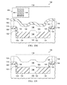
Referring to FIG. 1R , a protective layer 166 is formed over the isolated semiconductor layer 114. The protective layer 166 may include, for example, 5 nanometers to 15 nanometers of thermal oxide. The protective layer 166 has different etch characteristics than the sidewalls 136 and a top layer of the blocking layer 104, for example the layer of silicon nitride 110.
Referring to FIG. 1S , the sidewalls 136 and the layer of silicon nitride 110 of the blocking layer 104 of FIG. 1R are removed. Silicon nitride in the sidewalls 136 and the layer of silicon nitride 110 may be removed by an aqueous solution of phosphoric acid at 150° C. A width 168 of the isolated semiconductor layer 114 may be, for example, 2 microns to 200 microns. A final thickness 170 of the buried isolation layer 124 may be, for example, 200 nanometers to 900 nanometers thick. Components such as transistors may subsequently be formed in the leaving the isolated semiconductor layer 114 over the buried isolation layer 124, advantageously having a low capacitance to the substrate 102.
Referring to FIG. 2B , the non-crystalline region 150 is formed over the blocking layer 104 and the buried isolation layer 124 and contacting the seed layer 144. In the instant example, the non-crystalline region 150 is formed as a layer of polycrystalline silicon 150, referred to as polysilicon. The polysilicon non-crystalline region 150 may be formed, for example, by thermal decomposition of silane at a temperature of 550° C. to 600° C. and a pressure of 0.2 torr to 1 torr. Forming the non-crystalline region 150 separately from the seed layer 144 may advantageously provide more thickness control for the non-crystalline region 150 compared to concurrent formation. The sidewalls 136 separate the non-crystalline region 150 from the substrate 102.
Referring to FIG. 2C , the cap layer 152 is formed over the non-crystalline region 150 as described in reference to FIG. 1L . The cap layer 152 may be formed so as to provide maximum anti-reflection properties for the subsequent radiant-induced recrystallization process in an area proximate to the seed layer 144, taking into account a shape of a top surface of the non-crystalline region 150.
Referring to FIG. 2D , the radiant-induced recrystallization process 154 heats the non-crystalline region 150 to a higher temperature than the seed layer 144 so that polysilicon in the non-crystalline region 150 forms the single-crystalline region 148 around the seed layer 144 and grows outward across the buried isolation layer 124. The radiant-induced recrystallization process 154 may produce a roughened interface 156 between the cap layer 152 and the newly recrystallized portion of the single-crystalline region 148. Forming the seed layer 144 to extend above the top surface 106 of the substrate 102 may enable the newly recrystallized portion of the single-crystalline region 148 over the buried isolation layer 124 to form with fewer defects than with a seed layer 144 coplanar with the top surface 126 of the buried isolation layer 124.
Referring to FIG. 2E , the cap layer 152 of FIG. 2D is removed without removing a significant portion of the single-crystalline region 148. The cap layer 152 may be removed as described in reference to FIG. 1N .
Referring to FIG. 2F , the single-crystalline region 148 and possibly the seed layer 144 are planarized to provide a smooth planar top surface 158. The single-crystalline region 148 and possibly the seed layer 144 may be planarized by a CMP process or by another method. The top surface 158 may be above the blocking layer 104 as depicted in FIG. 2F . In another version of the instant example, the top surface 158 may be substantially coplanar with a top surface of the blocking layer 104, as may result from a CMP planarization process. In a further version, the top surface 158 may be below the top surface of the blocking layer 104 but above the top surface 106 of the substrate 102 adjacent to the isolation recess 118.
Referring to FIG. 2G , the single-crystalline region 148 is recessed in the isolation recess 118 to provide a desired thickness 164. The single-crystalline region 148 may be recessed by a timed plasma etch process 172 as depicted in FIG. 2G , or possibly by a timed wet etch process using an aqueous buffered solution of hydrofluoric acid. After the desired thickness 164 is attained, process of the integrated circuit 100 continues as described in reference to FIG. 1R et seq.
While various embodiments of the present invention have been described above, it should be understood that they have been presented by way of example only and not limitation. Numerous changes to the disclosed embodiments can be made in accordance with the disclosure herein without departing from the spirit or scope of the invention. Thus, the breadth and scope of the present invention should not be limited by any of the above described embodiments. Rather, the scope of the invention should be defined in accordance with the following claims and their equivalents.
Claims (15)
1. An integrated circuit, comprising:
a bulk silicon wafer consisting essentially of silicon single crystal semiconductor material, wherein the bulk silicon wafer has a recess formed below a top surface of the bulk silicon wafer, the recess having sidewalls and a bottom;
a buried dielectric layer formed at the bottom of the recess, the buried dielectric layer having a trench;
an epitaxial silicon layer at least partly overlying the buried dielectric layer, wherein: to the extent that the epitaxial silicon layer overlies the buried dielectric layer, the epitaxial silicon layer consists essentially of single-crystalline material, at least a portion of the single-crystalline material being formed by radiant-induced recrystallization of non-crystalline material; and
a single-crystal silicon-based seed layer completely filling the trench and extending between the bulk silicon wafer and the epitaxial silicon layer.
2. The integrated circuit of claim 1 , comprising a dielectric layer over the epitaxial silicon layer.
3. The integrated circuit of claim 1 , comprising a dielectric layer between the epitaxial silicon layer and the sidewalls of the recess.
4. The integrated circuit of claim 1 , wherein the silicon-based seed layer is formed by selective epitaxial growth.
5. The integrated circuit of claim 4 , wherein the silicon-based seed layer is adjacent at least a portion of the single-crystalline material.
6. The integrated circuit of claim 1 , wherein a top surface of the epitaxial silicon layer is substantially coplanar with the top surface of the bulk silicon wafer.
7. The integrated circuit of claim 1 , wherein the buried dielectric layer comprises silicon dioxide.
8. The integrated circuit of claim 1 , wherein the buried dielectric layer comprises a plurality of sublayers of different dielectric materials.
9. The integrated circuit of claim 1 , wherein the epitaxial silicon layer is formed by non-selective epitaxial growth.
10. An integrated circuit, comprising:
a bulk silicon wafer consisting essentially of silicon single crystal semiconductor material, wherein the bulk silicon wafer has a recess formed below a top surface of the bulk silicon wafer, the recess having sidewalls and a bottom;
a buried dielectric layer formed at the bottom of the recess, the buried dielectric layer having a trench;
an epitaxial silicon layer formed by non-selective epitaxial growth, and at least partly overlying the buried dielectric layer, wherein: to the extent that the epitaxial silicon layer overlies the buried dielectric layer, the epitaxial silicon layer consists essentially of single-crystalline material, at least a portion of the single-crystalline material being formed by radiant-induced recrystallization of non-crystalline material; and
a single-crystal silicon-based seed layer formed by selective epitaxial growth, completely filling the trench, extending between the bulk silicon wafer and the epitaxial silicon layer, and adjacent at least a portion of the single-crystalline material.
11. The integrated circuit of claim 10 , comprising a dielectric layer over the epitaxial silicon layer.
12. The integrated circuit of claim 10 , comprising a dielectric layer between the epitaxial silicon layer and the sidewalls of the recess.
13. The integrated circuit of claim 10 , wherein a top surface of the epitaxial silicon layer is substantially coplanar with the top surface of the bulk silicon wafer.
14. The integrated circuit of claim 10 , wherein the buried dielectric layer comprises silicon dioxide.
15. The integrated circuit of claim 10 , wherein the buried dielectric layer comprises a plurality of sublayers of different dielectric materials.
Priority Applications (2)
| Application Number | Priority Date | Filing Date | Title |
|---|---|---|---|
| US15/090,000 US10032863B2 (en) | 2014-04-13 | 2016-04-04 | Isolated semiconductor layer in bulk wafer by localized silicon epitaxial seed formation |
| US16/027,522 US10516019B2 (en) | 2014-04-13 | 2018-07-05 | Isolated semiconductor layer in bulk wafer by localized silicon epitaxial seed formation |
Applications Claiming Priority (3)
| Application Number | Priority Date | Filing Date | Title |
|---|---|---|---|
| US201461978935P | 2014-04-13 | 2014-04-13 | |
| US14/301,788 US9330959B2 (en) | 2014-04-13 | 2014-06-11 | Isolated semiconductor layer in bulk wafer by localized silicon epitaxial seed formation |
| US15/090,000 US10032863B2 (en) | 2014-04-13 | 2016-04-04 | Isolated semiconductor layer in bulk wafer by localized silicon epitaxial seed formation |
Related Parent Applications (1)
| Application Number | Title | Priority Date | Filing Date |
|---|---|---|---|
| US14/301,788 Continuation US9330959B2 (en) | 2014-04-13 | 2014-06-11 | Isolated semiconductor layer in bulk wafer by localized silicon epitaxial seed formation |
Related Child Applications (1)
| Application Number | Title | Priority Date | Filing Date |
|---|---|---|---|
| US16/027,522 Continuation US10516019B2 (en) | 2014-04-13 | 2018-07-05 | Isolated semiconductor layer in bulk wafer by localized silicon epitaxial seed formation |
Publications (2)
| Publication Number | Publication Date |
|---|---|
| US20160218177A1 US20160218177A1 (en) | 2016-07-28 |
| US10032863B2 true US10032863B2 (en) | 2018-07-24 |
Family
ID=54265679
Family Applications (3)
| Application Number | Title | Priority Date | Filing Date |
|---|---|---|---|
| US14/301,788 Active 2034-09-06 US9330959B2 (en) | 2014-04-13 | 2014-06-11 | Isolated semiconductor layer in bulk wafer by localized silicon epitaxial seed formation |
| US15/090,000 Active US10032863B2 (en) | 2014-04-13 | 2016-04-04 | Isolated semiconductor layer in bulk wafer by localized silicon epitaxial seed formation |
| US16/027,522 Active US10516019B2 (en) | 2014-04-13 | 2018-07-05 | Isolated semiconductor layer in bulk wafer by localized silicon epitaxial seed formation |
Family Applications Before (1)
| Application Number | Title | Priority Date | Filing Date |
|---|---|---|---|
| US14/301,788 Active 2034-09-06 US9330959B2 (en) | 2014-04-13 | 2014-06-11 | Isolated semiconductor layer in bulk wafer by localized silicon epitaxial seed formation |
Family Applications After (1)
| Application Number | Title | Priority Date | Filing Date |
|---|---|---|---|
| US16/027,522 Active US10516019B2 (en) | 2014-04-13 | 2018-07-05 | Isolated semiconductor layer in bulk wafer by localized silicon epitaxial seed formation |
Country Status (5)
| Country | Link |
|---|---|
| US (3) | US9330959B2 (en) |
| EP (1) | EP3132468B1 (en) |
| JP (3) | JP2017511610A (en) |
| CN (2) | CN116646315A (en) |
| WO (1) | WO2015160714A1 (en) |
Cited By (1)
| Publication number | Priority date | Publication date | Assignee | Title |
|---|---|---|---|---|
| US20180315816A1 (en) * | 2014-04-13 | 2018-11-01 | Texas Instruments Incorporated | Isolated semiconductor layer in bulk wafer by localized silicon epitaxial seed formation |
Families Citing this family (3)
| Publication number | Priority date | Publication date | Assignee | Title |
|---|---|---|---|---|
| CN107527815B (en) * | 2016-06-21 | 2022-03-22 | 蓝枪半导体有限责任公司 | Method for manufacturing epitaxial layer |
| CN107958933B (en) * | 2016-10-17 | 2020-05-26 | 中芯国际集成电路制造(北京)有限公司 | Semiconductor device and method of manufacturing the same |
| US20230420546A1 (en) * | 2022-06-24 | 2023-12-28 | Nxp Usa, Inc. | Transistor with current terminal regions and channel region in layer over dielectric |
Citations (21)
| Publication number | Priority date | Publication date | Assignee | Title |
|---|---|---|---|---|
| US4749441A (en) * | 1986-12-11 | 1988-06-07 | General Motors Corporation | Semiconductor mushroom structure fabrication |
| US4952526A (en) * | 1988-04-05 | 1990-08-28 | Thomson-Csf | Method for the fabrication of an alternation of layers of monocrystalline semiconducting material and layers of insulating material |
| US5891763A (en) * | 1997-10-22 | 1999-04-06 | Wanlass; Frank M. | Damascene pattering of SOI MOS transistors |
| US6403427B2 (en) * | 1997-10-28 | 2002-06-11 | Stmicroelectronics, Inc. | Field effect transistor having dielectrically isolated sources and drains and method for making same |
| US6660582B2 (en) * | 2001-10-12 | 2003-12-09 | Infineon Technologies Ag | Method of forming a vertical field-effect transistor device |
| US20050236687A1 (en) | 2004-04-22 | 2005-10-27 | International Business Machines Corporation | Strained silicon CMOS on hybrid crystal orientations |
| US7001804B2 (en) * | 2004-01-30 | 2006-02-21 | Atmel Germany Gmbh | Method of producing active semiconductor layers of different thicknesses in an SOI wafer |
| US20080220586A1 (en) | 2005-10-28 | 2008-09-11 | International Business Machines Corporation | Methods for forming semiconductor structures with buried isolation collars and semiconductor structures formed by these methods |
| US20080274595A1 (en) | 2007-05-01 | 2008-11-06 | Spencer Gregory S | Dual substrate orientation or bulk on SOI integrations using oxidation for silicon epitaxy spacer formation |
| US20080274594A1 (en) | 2007-05-01 | 2008-11-06 | Karve Gauri V | Step height reduction between SOI and EPI for DSO and BOS integration |
| US7495287B2 (en) * | 2006-01-31 | 2009-02-24 | Seiko Epson Corporation | Semiconductor device and manufacturing method thereof |
| US7611937B2 (en) | 2005-06-24 | 2009-11-03 | Taiwan Semiconductor Manufacturing Company, Ltd. | High performance transistors with hybrid crystal orientations |
| US20100200907A1 (en) | 2009-02-11 | 2010-08-12 | Dong Chul Yoo | Semiconductor Integrated Circuit Device and Method of Fabricating the Same |
| US20100276735A1 (en) | 2009-04-30 | 2010-11-04 | Spencer Gregory S | Semiconductor device with photonics |
| US20110210389A1 (en) | 2010-02-26 | 2011-09-01 | Globalfoundries Inc. | Transistor Comprising a Buried High-K Metal Gate Electrode Structure |
| US20120223420A1 (en) * | 2009-12-23 | 2012-09-06 | Infineon Technologies Austria Ag | Semiconductor body with a buried material layer |
| US20130029449A1 (en) | 2008-09-24 | 2013-01-31 | Taiwan Semiconductor Manufacturing Company, Ltd. | Semiconductor Sensor Structures with Reduced Dislocation Defect Densities and Related Methods for the Same |
| GB2494739A (en) | 2011-09-15 | 2013-03-20 | Ibm | Trench isolation structure |
| US20130256758A1 (en) | 2012-03-30 | 2013-10-03 | International Business Machines Corporation | Integrated circuit structure having air-gap trench isolation and related design structure |
| US20130277854A1 (en) | 2012-04-23 | 2013-10-24 | Globalfoundries Inc. | 3d integrated circuit system with connecting via structure and method for forming the same |
| US8993420B2 (en) | 2013-03-11 | 2015-03-31 | Samsung Electronics Co., Ltd. | Methods of forming epitaxial layers |
Family Cites Families (18)
| Publication number | Priority date | Publication date | Assignee | Title |
|---|---|---|---|---|
| JPS594048A (en) * | 1982-06-30 | 1984-01-10 | Toshiba Corp | Fabrication of semiconductor device |
| JPS63131510A (en) * | 1986-11-21 | 1988-06-03 | Hitachi Ltd | Method of forming single crystal thin film |
| JPH0281422A (en) * | 1988-09-16 | 1990-03-22 | Fuji Electric Co Ltd | Manufacture of soi substrate |
| US5017999A (en) * | 1989-06-30 | 1991-05-21 | Honeywell Inc. | Method for forming variable width isolation structures |
| US5143862A (en) * | 1990-11-29 | 1992-09-01 | Texas Instruments Incorporated | SOI wafer fabrication by selective epitaxial growth |
| JPH1092922A (en) * | 1996-09-10 | 1998-04-10 | Sony Corp | Semiconductor device manufacturing method and semiconductor device |
| EP1049156B1 (en) * | 1999-04-30 | 2009-02-18 | STMicroelectronics S.r.l. | Manufacturing process of integrated SOI circuit structures |
| JP2002359290A (en) * | 2001-03-27 | 2002-12-13 | Matsushita Electric Ind Co Ltd | Semiconductor integrated device |
| US6627510B1 (en) * | 2002-03-29 | 2003-09-30 | Sharp Laboratories Of America, Inc. | Method of making self-aligned shallow trench isolation |
| KR100426442B1 (en) * | 2002-05-13 | 2004-04-13 | 주식회사 하이닉스반도체 | A method for forming a transistor of a semiconductor device |
| KR100611076B1 (en) * | 2005-07-15 | 2006-08-09 | 삼성전자주식회사 | Stacked semiconductor device and manufacturing method thereof |
| KR100703033B1 (en) * | 2006-03-22 | 2007-04-09 | 삼성전자주식회사 | Semiconductor device and manufacturing method thereof |
| US7435639B2 (en) * | 2006-05-31 | 2008-10-14 | Freescale Semiconductor, Inc. | Dual surface SOI by lateral epitaxial overgrowth |
| JP2008159691A (en) * | 2006-12-21 | 2008-07-10 | Rohm Co Ltd | Nitride semiconductor element, nitride semiconductor crystal growth substrate, and method for manufacturing same |
| US8815654B2 (en) * | 2007-06-14 | 2014-08-26 | International Business Machines Corporation | Vertical current controlled silicon on insulator (SOI) device such as a silicon controlled rectifier and method of forming vertical SOI current controlled devices |
| JP5353016B2 (en) * | 2008-01-22 | 2013-11-27 | 株式会社デンソー | Semiconductor device |
| US9806190B2 (en) * | 2010-10-28 | 2017-10-31 | Texas Instruments Incorporated | High voltage drain extension on thin buried oxide SOI |
| US9330959B2 (en) * | 2014-04-13 | 2016-05-03 | Texas Instruments Incorporated | Isolated semiconductor layer in bulk wafer by localized silicon epitaxial seed formation |
-
2014
- 2014-06-11 US US14/301,788 patent/US9330959B2/en active Active
-
2015
- 2015-04-13 JP JP2016562495A patent/JP2017511610A/en active Pending
- 2015-04-13 CN CN202310673929.XA patent/CN116646315A/en active Pending
- 2015-04-13 CN CN201580018939.3A patent/CN106233452B8/en active Active
- 2015-04-13 WO PCT/US2015/025593 patent/WO2015160714A1/en not_active Ceased
- 2015-04-13 EP EP15780680.3A patent/EP3132468B1/en active Active
-
2016
- 2016-04-04 US US15/090,000 patent/US10032863B2/en active Active
-
2018
- 2018-07-05 US US16/027,522 patent/US10516019B2/en active Active
-
2019
- 2019-08-05 JP JP2019143488A patent/JP7137538B2/en active Active
- 2019-12-27 JP JP2019238830A patent/JP6993547B2/en active Active
Patent Citations (21)
| Publication number | Priority date | Publication date | Assignee | Title |
|---|---|---|---|---|
| US4749441A (en) * | 1986-12-11 | 1988-06-07 | General Motors Corporation | Semiconductor mushroom structure fabrication |
| US4952526A (en) * | 1988-04-05 | 1990-08-28 | Thomson-Csf | Method for the fabrication of an alternation of layers of monocrystalline semiconducting material and layers of insulating material |
| US5891763A (en) * | 1997-10-22 | 1999-04-06 | Wanlass; Frank M. | Damascene pattering of SOI MOS transistors |
| US6403427B2 (en) * | 1997-10-28 | 2002-06-11 | Stmicroelectronics, Inc. | Field effect transistor having dielectrically isolated sources and drains and method for making same |
| US6660582B2 (en) * | 2001-10-12 | 2003-12-09 | Infineon Technologies Ag | Method of forming a vertical field-effect transistor device |
| US7001804B2 (en) * | 2004-01-30 | 2006-02-21 | Atmel Germany Gmbh | Method of producing active semiconductor layers of different thicknesses in an SOI wafer |
| US20050236687A1 (en) | 2004-04-22 | 2005-10-27 | International Business Machines Corporation | Strained silicon CMOS on hybrid crystal orientations |
| US7611937B2 (en) | 2005-06-24 | 2009-11-03 | Taiwan Semiconductor Manufacturing Company, Ltd. | High performance transistors with hybrid crystal orientations |
| US20080220586A1 (en) | 2005-10-28 | 2008-09-11 | International Business Machines Corporation | Methods for forming semiconductor structures with buried isolation collars and semiconductor structures formed by these methods |
| US7495287B2 (en) * | 2006-01-31 | 2009-02-24 | Seiko Epson Corporation | Semiconductor device and manufacturing method thereof |
| US20080274594A1 (en) | 2007-05-01 | 2008-11-06 | Karve Gauri V | Step height reduction between SOI and EPI for DSO and BOS integration |
| US20080274595A1 (en) | 2007-05-01 | 2008-11-06 | Spencer Gregory S | Dual substrate orientation or bulk on SOI integrations using oxidation for silicon epitaxy spacer formation |
| US20130029449A1 (en) | 2008-09-24 | 2013-01-31 | Taiwan Semiconductor Manufacturing Company, Ltd. | Semiconductor Sensor Structures with Reduced Dislocation Defect Densities and Related Methods for the Same |
| US20100200907A1 (en) | 2009-02-11 | 2010-08-12 | Dong Chul Yoo | Semiconductor Integrated Circuit Device and Method of Fabricating the Same |
| US20100276735A1 (en) | 2009-04-30 | 2010-11-04 | Spencer Gregory S | Semiconductor device with photonics |
| US20120223420A1 (en) * | 2009-12-23 | 2012-09-06 | Infineon Technologies Austria Ag | Semiconductor body with a buried material layer |
| US20110210389A1 (en) | 2010-02-26 | 2011-09-01 | Globalfoundries Inc. | Transistor Comprising a Buried High-K Metal Gate Electrode Structure |
| GB2494739A (en) | 2011-09-15 | 2013-03-20 | Ibm | Trench isolation structure |
| US20130256758A1 (en) | 2012-03-30 | 2013-10-03 | International Business Machines Corporation | Integrated circuit structure having air-gap trench isolation and related design structure |
| US20130277854A1 (en) | 2012-04-23 | 2013-10-24 | Globalfoundries Inc. | 3d integrated circuit system with connecting via structure and method for forming the same |
| US8993420B2 (en) | 2013-03-11 | 2015-03-31 | Samsung Electronics Co., Ltd. | Methods of forming epitaxial layers |
Non-Patent Citations (2)
| Title |
|---|
| European Search Report for EU 15780680.3 dated Oct. 19, 2017. |
| International Search Report in corresponding PCT Application No. PCT/US2015/025593, dated Jul. 16, 2015 (2 pages). |
Cited By (2)
| Publication number | Priority date | Publication date | Assignee | Title |
|---|---|---|---|---|
| US20180315816A1 (en) * | 2014-04-13 | 2018-11-01 | Texas Instruments Incorporated | Isolated semiconductor layer in bulk wafer by localized silicon epitaxial seed formation |
| US10516019B2 (en) * | 2014-04-13 | 2019-12-24 | Texas Instruments Incorporated | Isolated semiconductor layer in bulk wafer by localized silicon epitaxial seed formation |
Also Published As
| Publication number | Publication date |
|---|---|
| CN106233452A (en) | 2016-12-14 |
| JP2020061577A (en) | 2020-04-16 |
| JP7137538B2 (en) | 2022-09-14 |
| CN106233452B8 (en) | 2023-08-15 |
| US20160218177A1 (en) | 2016-07-28 |
| US20150294902A1 (en) | 2015-10-15 |
| EP3132468A1 (en) | 2017-02-22 |
| EP3132468A4 (en) | 2017-11-22 |
| EP3132468B1 (en) | 2024-04-10 |
| US20180315816A1 (en) | 2018-11-01 |
| CN106233452B (en) | 2023-06-30 |
| JP6993547B2 (en) | 2022-01-13 |
| JP2019220696A (en) | 2019-12-26 |
| JP2017511610A (en) | 2017-04-20 |
| US9330959B2 (en) | 2016-05-03 |
| CN116646315A (en) | 2023-08-25 |
| US10516019B2 (en) | 2019-12-24 |
| WO2015160714A1 (en) | 2015-10-22 |
Similar Documents
| Publication | Publication Date | Title |
|---|---|---|
| US9673222B2 (en) | Fin isolation structures facilitating different fin isolation schemes | |
| US9941406B2 (en) | FinFETs with source/drain cladding | |
| US10516019B2 (en) | Isolated semiconductor layer in bulk wafer by localized silicon epitaxial seed formation | |
| US20150014807A1 (en) | Method of forming a shallow trench isolation structure | |
| US20150311111A1 (en) | Fin Structure of Semiconductor Device | |
| US9401373B2 (en) | Multi-fin finFETs with merged-fin source/drains and replacement gates | |
| CN102347352A (en) | Semiconductor device and manufacturing method thereof | |
| CN103295950A (en) | Shallow groove isolating structure manufacturing method | |
| US20210225711A1 (en) | High mobility transistors | |
| US10115638B2 (en) | Partially recessed channel core transistors in replacement gate flow | |
| TW202038379A (en) | Methods of forming semiconductor devices | |
| CN101630655B (en) | Method of forming shallow trench isolation | |
| US10886164B2 (en) | Isolated semiconductor layer over buried isolation layer | |
| CN101996921B (en) | STI forming method | |
| US9312164B2 (en) | Localized region of isolated silicon over dielectric mesa | |
| US9466520B2 (en) | Localized region of isolated silicon over recessed dielectric layer | |
| US9093560B2 (en) | Gate height uniformity in semiconductor devices | |
| US8193056B2 (en) | Method of manufacturing semiconductor device | |
| US9224657B2 (en) | Hard mask for source/drain epitaxy control | |
| CN105206576B (en) | Method for forming embedded germanium silicon source/drain structure | |
| TW201717281A (en) | Semiconductor component and manufacturing method thereof |
Legal Events
| Date | Code | Title | Description |
|---|---|---|---|
| STCF | Information on status: patent grant |
Free format text: PATENTED CASE |
|
| MAFP | Maintenance fee payment |
Free format text: PAYMENT OF MAINTENANCE FEE, 4TH YEAR, LARGE ENTITY (ORIGINAL EVENT CODE: M1551); ENTITY STATUS OF PATENT OWNER: LARGE ENTITY Year of fee payment: 4 |
|
| MAFP | Maintenance fee payment |
Free format text: PAYMENT OF MAINTENANCE FEE, 8TH YEAR, LARGE ENTITY (ORIGINAL EVENT CODE: M1552); ENTITY STATUS OF PATENT OWNER: LARGE ENTITY Year of fee payment: 8 |