US10014435B2 - Method for manufacturing metallic reflector for LED package - Google Patents
Method for manufacturing metallic reflector for LED package Download PDFInfo
- Publication number
- US10014435B2 US10014435B2 US14/716,313 US201514716313A US10014435B2 US 10014435 B2 US10014435 B2 US 10014435B2 US 201514716313 A US201514716313 A US 201514716313A US 10014435 B2 US10014435 B2 US 10014435B2
- Authority
- US
- United States
- Prior art keywords
- reflector
- lower body
- stamping
- led chip
- metal plate
- Prior art date
- Legal status (The legal status is an assumption and is not a legal conclusion. Google has not performed a legal analysis and makes no representation as to the accuracy of the status listed.)
- Active, expires
Links
Images


Classifications
-
- H—ELECTRICITY
- H10—SEMICONDUCTOR DEVICES; ELECTRIC SOLID-STATE DEVICES NOT OTHERWISE PROVIDED FOR
- H10H—INORGANIC LIGHT-EMITTING SEMICONDUCTOR DEVICES HAVING POTENTIAL BARRIERS
- H10H20/00—Individual inorganic light-emitting semiconductor devices having potential barriers, e.g. light-emitting diodes [LED]
- H10H20/01—Manufacture or treatment
-
- H01L33/005—
-
- H01L33/60—
-
- H—ELECTRICITY
- H10—SEMICONDUCTOR DEVICES; ELECTRIC SOLID-STATE DEVICES NOT OTHERWISE PROVIDED FOR
- H10H—INORGANIC LIGHT-EMITTING SEMICONDUCTOR DEVICES HAVING POTENTIAL BARRIERS
- H10H20/00—Individual inorganic light-emitting semiconductor devices having potential barriers, e.g. light-emitting diodes [LED]
- H10H20/80—Constructional details
- H10H20/85—Packages
- H10H20/855—Optical field-shaping means, e.g. lenses
- H10H20/856—Reflecting means
-
- B—PERFORMING OPERATIONS; TRANSPORTING
- B21—MECHANICAL METAL-WORKING WITHOUT ESSENTIALLY REMOVING MATERIAL; PUNCHING METAL
- B21D—WORKING OR PROCESSING OF SHEET METAL OR METAL TUBES, RODS OR PROFILES WITHOUT ESSENTIALLY REMOVING MATERIAL; PUNCHING METAL
- B21D28/00—Shaping by press-cutting; Perforating
- B21D28/02—Punching blanks or articles with or without obtaining scrap; Notching
-
- B—PERFORMING OPERATIONS; TRANSPORTING
- B21—MECHANICAL METAL-WORKING WITHOUT ESSENTIALLY REMOVING MATERIAL; PUNCHING METAL
- B21D—WORKING OR PROCESSING OF SHEET METAL OR METAL TUBES, RODS OR PROFILES WITHOUT ESSENTIALLY REMOVING MATERIAL; PUNCHING METAL
- B21D28/00—Shaping by press-cutting; Perforating
- B21D28/24—Perforating, i.e. punching holes
- B21D28/32—Perforating, i.e. punching holes in other articles of special shape
-
- B—PERFORMING OPERATIONS; TRANSPORTING
- B21—MECHANICAL METAL-WORKING WITHOUT ESSENTIALLY REMOVING MATERIAL; PUNCHING METAL
- B21D—WORKING OR PROCESSING OF SHEET METAL OR METAL TUBES, RODS OR PROFILES WITHOUT ESSENTIALLY REMOVING MATERIAL; PUNCHING METAL
- B21D35/00—Combined processes according to or processes combined with methods covered by groups B21D1/00 - B21D31/00
- B21D35/001—Shaping combined with punching, e.g. stamping and perforating
-
- F—MECHANICAL ENGINEERING; LIGHTING; HEATING; WEAPONS; BLASTING
- F21—LIGHTING
- F21K—NON-ELECTRIC LIGHT SOURCES USING LUMINESCENCE; LIGHT SOURCES USING ELECTROCHEMILUMINESCENCE; LIGHT SOURCES USING CHARGES OF COMBUSTIBLE MATERIAL; LIGHT SOURCES USING SEMICONDUCTOR DEVICES AS LIGHT-GENERATING ELEMENTS; LIGHT SOURCES NOT OTHERWISE PROVIDED FOR
- F21K9/00—Light sources using semiconductor devices as light-generating elements, e.g. using light-emitting diodes [LED] or lasers
- F21K9/60—Optical arrangements integrated in the light source, e.g. for improving the colour rendering index or the light extraction
- F21K9/68—Details of reflectors forming part of the light source
-
- F—MECHANICAL ENGINEERING; LIGHTING; HEATING; WEAPONS; BLASTING
- F21—LIGHTING
- F21K—NON-ELECTRIC LIGHT SOURCES USING LUMINESCENCE; LIGHT SOURCES USING ELECTROCHEMILUMINESCENCE; LIGHT SOURCES USING CHARGES OF COMBUSTIBLE MATERIAL; LIGHT SOURCES USING SEMICONDUCTOR DEVICES AS LIGHT-GENERATING ELEMENTS; LIGHT SOURCES NOT OTHERWISE PROVIDED FOR
- F21K9/00—Light sources using semiconductor devices as light-generating elements, e.g. using light-emitting diodes [LED] or lasers
- F21K9/90—Methods of manufacture
-
- H01L2224/48091—
-
- H01L2224/48247—
-
- H01L2924/00014—
-
- H01L2933/0025—
-
- H01L2933/0033—
-
- H01L2933/0058—
-
- H—ELECTRICITY
- H10—SEMICONDUCTOR DEVICES; ELECTRIC SOLID-STATE DEVICES NOT OTHERWISE PROVIDED FOR
- H10H—INORGANIC LIGHT-EMITTING SEMICONDUCTOR DEVICES HAVING POTENTIAL BARRIERS
- H10H20/00—Individual inorganic light-emitting semiconductor devices having potential barriers, e.g. light-emitting diodes [LED]
- H10H20/01—Manufacture or treatment
- H10H20/034—Manufacture or treatment of coatings
-
- H—ELECTRICITY
- H10—SEMICONDUCTOR DEVICES; ELECTRIC SOLID-STATE DEVICES NOT OTHERWISE PROVIDED FOR
- H10H—INORGANIC LIGHT-EMITTING SEMICONDUCTOR DEVICES HAVING POTENTIAL BARRIERS
- H10H20/00—Individual inorganic light-emitting semiconductor devices having potential barriers, e.g. light-emitting diodes [LED]
- H10H20/01—Manufacture or treatment
- H10H20/036—Manufacture or treatment of packages
- H10H20/0363—Manufacture or treatment of packages of optical field-shaping means
-
- H—ELECTRICITY
- H10—SEMICONDUCTOR DEVICES; ELECTRIC SOLID-STATE DEVICES NOT OTHERWISE PROVIDED FOR
- H10W—GENERIC PACKAGES, INTERCONNECTIONS, CONNECTORS OR OTHER CONSTRUCTIONAL DETAILS OF DEVICES COVERED BY CLASS H10
- H10W90/00—Package configurations
- H10W90/701—Package configurations characterised by the relative positions of pads or connectors relative to package parts
- H10W90/751—Package configurations characterised by the relative positions of pads or connectors relative to package parts of bond wires
- H10W90/756—Package configurations characterised by the relative positions of pads or connectors relative to package parts of bond wires between a chip and a stacked lead frame, conducting package substrate or heat sink
-
- Y—GENERAL TAGGING OF NEW TECHNOLOGICAL DEVELOPMENTS; GENERAL TAGGING OF CROSS-SECTIONAL TECHNOLOGIES SPANNING OVER SEVERAL SECTIONS OF THE IPC; TECHNICAL SUBJECTS COVERED BY FORMER USPC CROSS-REFERENCE ART COLLECTIONS [XRACs] AND DIGESTS
- Y10—TECHNICAL SUBJECTS COVERED BY FORMER USPC
- Y10T—TECHNICAL SUBJECTS COVERED BY FORMER US CLASSIFICATION
- Y10T29/00—Metal working
- Y10T29/49—Method of mechanical manufacture
- Y10T29/4998—Combined manufacture including applying or shaping of fluent material
- Y10T29/49988—Metal casting
Definitions
- the present invention is related to a metallic reflector manufacturing method for an LED package. More particularly, the present invention relates to a metallic reflector manufacturing method for an LED package that the manufacturing process is very simple and the cost is cheap.
- an LED Light Emitting Diode
- the LED uses low voltage and current to enable continuous light emitting and has many merits such as low power consumption compared to other light source.
- the LED is manufactured to have a general package structure, as shown in FIG. 1 , the manufactured LED package 1 includes a first lid frame 12 and a second lid frame 13 , and a package body 11 that is integrally formed with the first and the second lid frame 12 and 13 .
- the package body 11 has an opening 15 that respectively exposes the first and the second lid frame 12 and 13 , and an LED chip 14 is disposed on a bottom surface of the opening 15 .
- An encapsulant 16 is charged in the opening 15 to close and seal the opening 15 .
- the LED chip 14 is bonded on the first lid frame 12 through conductive adhesive and is connected to the second lid frame 13 through a bonding wire (W).
- An inner wall 111 of the opening 15 has a predetermined slant surface such that the light emitted from the LED chip 14 is reflected to the outside.
- the inner wall 111 of the opening 15 includes a synthetic resin such as PPA, the color thereof is changed by the light and the heat that are emitted from the LED chip 14 , the reflection rate is deteriorated, and therefore it is hard to realize desirable light efficiency.
- a metallic reflector surrounding the LED chip is mounted on a substrate so as to resolve the problem such that the color change problem and the reflection deterioration that is caused by the heat and the light of the LED chip are improved by a Korean Patent Laid-Open Publication No. 10-2009-0103292.
- FIG. 2 A plane figure of the improved ‘LED package’ is shown in FIG. 2 and a sectional view that is cut along a line I-I of FIG. 2 is shown in FIG. 3 .
- the LED package 2 includes a substrate 21 , and the substrate 21 has a pair of electrode pattern 22 and 23 , and an LED chip 24 is disposed on an upper surface of the substrate 21 .
- the LED chip 24 is connected to the other side electrode pattern 23 through a bonding wire (W) and is electrically connected to the pair of the electrode pattern 22 and 23 .
- the reflector is made of, for example, ring shape metallic material that is bonded by on the substrate 21 by adhesive.
- a bottom surface of the reflector 28 can be bonded to the pair of electrode pattern 22 and 23 by insulation adhesive, and the inner wall of the reflector 28 has a predetermined slant surface to reflect the light that is emitted from the LED chip 24 to the outside.
- a reflection layer 282 that is coated by a metal is formed on the inner wall 281 , and the reflection layer 282 is formed by, for example, aluminization.
- an encapsulant 26 of light penetration type resin for example, silicone resin, or epoxy resin is charged in the reflector 28 to close and seal the LED chip 24 that is disposed on the substrate 21 .
- the reflector 28 of metallic material that is applied to the LED package improves the color change problem and the reflection rate that are caused by the light and the heat of the LED chip 24 .
- the reflection layer 282 of the metallic reflector 28 is formed by aluminization
- the aluminization is direct performed on the metallic surface, and therefore the reflection layer 282 is lifted such that the reflection performance is deteriorated and the product quality is ruined.
- FIG. 4 An exemplary embodiment of a ‘molding type LED package’ that a reflector is molded by resin molding material to fix the reflector is shown in FIG. 4 .
- a molding type LED package 1 a includes a housing 10 that is formed by molding, for example, PPA resin, lid frame 22 a and 24 a having plurality of lids, an encapsulant 30 of light penetrating type that epoxy, silicone, or the mixture thereof is used to charge a cavity 12 space that an LED chip (not shown) is housed, and a reflector 40 that is made of metallic material and a reflection portion 42 and a heat radiating portion 44 are integrally formed.
- a metallic reflector 40 having a heat radiating portion 44 is disposed on the said molding type LED package, and the heating radiating problem is resolved and simultaneously the reflector 40 can be fixed on the lid frame 22 a and 24 a.
- the reflector 40 is sealed by the housing 10 and the encapsulant 30 , it is yet hard to radiate heat to the outside such that the performance, the durability, and the reliability of the LED package 1 are deteriorated.
- a plating layer that is plated on a reflection surface of the reflection portion 42 can be lifted by high temperature heat.
- the metallic reflector 28 and 40 are manufactured by a die casting forming.
- Zn material for making the reflector 28 and 40 are prepared, and the prepared material is melted in a melting furnace.
- the melted material is injected into a die at high pressure, the forming is completed, the reflector product is drawn from the die casting mold, and a trimming process is performed.
- the entire of the reflector product or the inner wall 281 and the reflection portion 42 is plated, and the plating process is performed as follows.
- the die casting forming needs an expensive facility due to metallic melted material, and also there is a problem that the die casting mold price is expensive.
- the conventional reflector is manufactured by the die casting forming, nonferrous metals such as Zn that the melting point is low has to be used, and therefore raw material cost is high, the process has to be mass production product, and there is a problem that the post processing is not easy.
- the inside constitution of the metal is weak and there is a problem that the product is weak from the high temperature or an impact.
- the present invention has been made in an effort to provide a metallic reflector manufacturing method for an LED package having advantages of simplifying the manufacturing process and reducing the manufacturing cost.
- a metallic reflector manufacturing method for an LED package of the present invention that a reflection surface is formed to surround an LED chip that is disposed on a substrate at a predetermined height and has a predetermined slant angle to reflect the light of the LED chip to the outside may include (a) preparing a metal plate, (b) processing a stamping reflector that includes a lower body and an upper body that is extended from an upper side of the lower body and is integrally formed with the lower body, a reflection surface that is slanted by a predetermined angle is formed at a central portion of the upper body and the lower body to reflect the light of the LED chip to the outside, and is processed by a stamping process such that a fixation portion is formed to fix the lower body on a substrate that the LED chip is mounted on, (c) sequentially plating Ni and Ag on the reflection surface or the stamping reflector surface, wherein the stamping processing of the step (b), may include (b-1) a piercing step that pierces a base hole
- multi-layered plating is formed on the metallic reflector surface such that the lifting of the plating can be prevented and the reflection performance of the reflector can be maintained.
- the metallic reflector can be manufactured by a stamping process, metallic melted liquid for a die casting forming is not necessary, and expensive facility and the die casting mold are not necessary.
- the reflector is manufactured by a stamping process, metal material can be variably selected, the manufacturing process becomes simple, and post processing such as plating can be easily performed.
- the manufacturing cost for the metallic reflector can be remarkably reduced.
- the constitution inside the metal is improved during the manufacturing and the reflector becomes strong for the high temperature and the outside impact.
- the performance, the durability, and the reliability of the LED package can be improved.
- FIG. 1 is a cross-sectional view of an LED package according to a conventional art.
- FIG. 2 is a plane view of a conventional LED package that improves a conventional art of FIG. 1 .
- FIG. 3 is a cross-sectional view showing a section along line I-I of FIG. 2 .
- FIG. 4 is a cross-sectional view of a conventional molding type LED package that a reflector is molded by resin molding material to fix the reflector.
- FIG. 5 is a front perspective view showing an exemplary embodiment of a metallic reflector that a metallic reflector manufacturing method for an LED package is applied thereto according to the present invention.
- FIG. 6 is a front view of FIG. 5 .
- FIG. 7 is a rear perspective view of FIG. 5 .
- FIG. 8 is a cross-sectional view showing an LED package that a metallic reflector of FIG. 5 is applied thereto.
- FIG. 9 is a front perspective view showing another exemplary embodiment of a metallic reflector that a metallic reflector manufacturing method for an LED package is applied thereto according to the present invention.
- FIG. 10 is a rear perspective view of FIG. 11 .
- FIG. 11 is a cross-sectional view showing an LED package that a metallic reflector is applied thereto of FIG. 9 .
- FIG. 12 is a schematic flowchart sequentially showing a metallic reflector manufacturing method for an LED package according to the present invention.
- FIG. 13 is a plane view of a metal plate that a metallic reflector manufacturing method for an LED package according to the present invention.
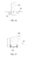
- FIG. 14 to FIG. 17 is a processing flowchart showing a stamping processing in a metal plate of FIG. 13 .
- FIG. 5 is a front perspective view showing an exemplary embodiment of a metallic reflector that a metallic reflector manufacturing method for an LED package is applied thereto according to the present invention
- FIG. 6 is a front view of FIG. 5
- FIG. 7 is a rear perspective view of FIG. 5 .
- FIG. 8 a cross-sectional view showing an LED package that a metallic reflector of FIG. 5 is applied thereto is shown in FIG. 8 .
- a metallic reflector 130 that a metallic reflector manufacturing method for an LED package is applied thereto includes a reflection surface that has a predetermined height to surround an LED chip 120 that is mounted on a substrate 110 and has a reflection surface that is slanted by a predetermined angle to reflect the light of the LED chip 120 to the outside.
- the metallic reflector 130 includes a lower body 134 that the lower surface thereof is bonded on a substrate 110 , an upper body 132 that is extended from an upper portion of the lower body 134 and a catching projection 132 a protrudes in a predetermined directions, and a catching portion 133 that faces each other at both sides of edges of the upper body 132 and a hook part 133 a protrudes toward an inner side at a lower end portion such that a reflector 130 can be fixed on a substrate 110 .
- a lower body 134 of a lower portion of the catching projection 132 a includes a taper 134 a and 134 b that becomes narrower as it goes to a lower side.
- a resin molding material is molded between an inner side (S) of the catching portion 133 and an outer side of the taper 134 a and 134 b of the lower body 134 of a lower side of the catching projection 132 a such that a metallic reflector 130 is securely fixed on a substrate 110 .
- the reflector 130 of metallic material can be further strongly fixed.
- a through hole 160 is formed at an inner surface of the lower body 134 and the upper body 132 such that the LED chip 120 of a substrate 110 is exposed outside the metallic reflector 130 , and a reflection surface is formed on an interior circumference of the through hole 160 .
- the reflection surface includes four main reflection surfaces 131 a and 131 b of substantially quadrangle shape and sub reflection surface 131 c that is formed at each edge of the main reflection surfaces 131 a and 131 b and has an area smaller than that of the main reflection surfaces.
- two reflection surfaces that face each other of the main reflection surfaces 131 a and 131 b has a slant angle increment surface 131 b that the slant angle thereof is increased in a predetermined height.
- the slant angle increment surface 131 b is formed at a surface that intersects in rectangular with the catching portion 133 during a stamping processing.
- the sub reflection surface 131 c is formed between the main reflection surfaces 131 a and 131 b , a reflection blind spot of a conventional rectangular edge is eliminated such that the reflection efficiency of the LED chip 120 can be improved.
- the slant angle increment surface 131 b is formed on the main reflection surfaces 131 a and 131 b of front and rear or left and right of the said reflections, for example, in a case that a shape (rectangle) or a mounting position of the LED chip 120 is changed, it deals with a case that the main reflection surfaces 131 a and 131 b are formed with an equal width.
- reference numerals 150 a and 150 b that are not described in FIG. 8 denotes a terminal lid.
- an inside hole (through hole 160 ) of the reflection surface is charged with an encapsulant (not shown).
- FIG. 9 A front perspective view of another exemplary embodiment of a metallic reflector that a metallic reflector manufacturing method for an LED package is applied thereto is shown in FIG. 9 according to the present invention, and a rear perspective view of FIG. 11 is shown in a FIG. 10 .
- FIG. 11 a cross sectional view showing an LED package that a metallic reflector of FIG. 9 is applied thereto is shown in FIG. 11 .
- the metallic reflector 300 that the metallic reflector manufacturing method for an LED package is applied thereto includes an upper body 301 and a lower body 302 that is extended in a lower portion of the upper body 301 and is integrally formed with the upper body 301 .
- a first opening 303 a which a reflection surface 303 having a predetermined angle is formed, is formed at a central portion of the upper body 301 and the lower body 302 , the light of the LED chip 120 that is disposed on the substrate 304 is reflected by the reflection surface 303 outside the metallic reflector 300 .
- a second opening 304 is formed inside a lower end portion of the lower body 302 , and the lower body 302 is fixedly inserted into an insertion hole 311 a of the substrate 311 . That is, the lower body 134 and 302 of the metallic reflector 130 according to an exemplary embodiment of FIG. 5 or a metallic reflector 300 according to an exemplary embodiment of FIG. 9 function as a fixation portion that is fixed on the substrate 110 and 304 .
- the metallic reflector 130 and 300 according to the present invention is fixed on the substrate 110 and 304 , the bonding strength of them is not less than that of the adhesive, the assembly of them is easy, and the structure of the metallic reflector 130 and 300 is reinforced.
- a schematic flowchart sequentially shows a metallic reflector manufacturing method for an LED package according to the present invention in FIG. 12 .
- a metallic reflector manufacturing method for an LED package according to the present invention as shown in FIG. 13 , a metal plate (e.g., Cu plate) 200 having a predetermined width, length, and thickness is prepared (step 410 ). Subsequently, the metallic reflector 130 of FIG. 5 or FIG. 9 is formed by a stamping process (Step 420 ).
- a metal plate e.g., Cu plate
- a reflector product 130 a is formed by a stamping process, wherein the reflector product 130 a includes a lower body 134 and 302 and an upper body 132 and 301 that is extended from an upper side of the lower body 134 and 302 and is integrally formed with the lower body 134 and 302 , reflection surfaces 131 a , 131 c , 303 that are slanted at a predetermined angle is formed at a central portion of the upper body 132 and 301 and the lower body 134 and 302 to reflect the light of the LED chip 120 to the outside, openings 160 and 303 a are formed at a lower portion of the reflection 131 a , 131 c , 303 to expose the LED chip 120 , and a fixation portion is formed to fix the lower body 134 and 302 on the substrate 110 and 304 that the LED chip 120 is mounted.
- Ni plating is formed on the surface of the refection surface 131 a , 131 c , 303 or the reflector product 130 a , and Ag plating is sequentially performed (Step 430 ).
- Cu strike plating of a thin film can be formed on the surface of the refection surface 131 a , 131 c , 303 or the reflector product 130 a within in a short time so as to improve the plating reliability.
- the metallic reflector 130 and 300 for the LED package according to the present invention is plated at least twice such that the lifting phenomenon of the surface plating layer of the reflection surface 131 a , 131 c , 303 or the reflector product 130 a can be prevented.
- an oxidation process or a color change prevention process is performed on the surface of the reflector product 130 a that is plated as described above (step 440 ).
- a manufacturing process of the metallic reflector 130 according the present invention is simple compared to a conventional process without the trimming process.
- the metal plate 200 can use Zn or Al besides Cu plate.
- the metal plate 200 can include Fe, Al, or Au besides the above element.
- a piercing (step 420 a ) is performed, wherein a base hole 201 for each course of a stamping process is formed at an upper and a lower edge of a metal plate in a length direction of the metal plate 200 by a piercing punch (not shown).
- a drawing punch 301 b of a stamping mold is used to perform a drawing (step 420 b ) that forms a reflection surface 131 a and 131 c on the metal plate 200 between the base holes 201 .
- a step portion is formed outside the lower body 134 and the upper body 132 to distinguish the lower body 134 and the upper body 132 .
- a first notch punch (not shown) of the stamping mold is used to perform a first notching (step 420 c ) to eliminate a scrap from the metal plate.
- a half etching punch 302 b of a stamping mold is used to perform a half etching (step 420 d ) to form a fixation portion or a catching portion 133 such as the lower body 134 .
- a second notching punch 303 b of a stamping mold is used to perform a second notching (step 420 e ) to form an opening 160 .
- a bending punch 350 b of the stamping mold is used to perform a bending to form a catching portion 133 .
- a cutting punch 306 b of a stamping mold is used to perform a cutting (step 420 f ) to eliminate unnecessary parts from the reflector product or to drop the reflector product 130 a from the metal plate 200 .
- the Ni plating and the Ag plating can be formed by one of a rack plating and a barrel plating. That is, the plating that is performed in a metallic reflector manufacturing method for a led package according to the present invention can be a rack plating that plates the metal plate 200 that the reflector product 130 a is formed as shown in FIG. 13 or can be a barrel plating that aggregates the reflector products to plate them after the cutting process.
Landscapes
- Led Device Packages (AREA)
Abstract
Description
Claims (1)
Applications Claiming Priority (2)
| Application Number | Priority Date | Filing Date | Title |
|---|---|---|---|
| KR10-2014-0061902 | 2014-05-22 | ||
| KR1020140061902A KR101444919B1 (en) | 2014-05-22 | 2014-05-22 | Method for manufacturing metallic reflector for led package |
Publications (2)
| Publication Number | Publication Date |
|---|---|
| US20150340545A1 US20150340545A1 (en) | 2015-11-26 |
| US10014435B2 true US10014435B2 (en) | 2018-07-03 |
Family
ID=51761251
Family Applications (1)
| Application Number | Title | Priority Date | Filing Date |
|---|---|---|---|
| US14/716,313 Active 2036-04-10 US10014435B2 (en) | 2014-05-22 | 2015-05-19 | Method for manufacturing metallic reflector for LED package |
Country Status (2)
| Country | Link |
|---|---|
| US (1) | US10014435B2 (en) |
| KR (1) | KR101444919B1 (en) |
Cited By (2)
| Publication number | Priority date | Publication date | Assignee | Title |
|---|---|---|---|---|
| US20170343187A1 (en) * | 2014-12-16 | 2017-11-30 | Enplas Corporation | Reflection Member, Illumination Device, Surface Light Source Device, Display Device, and Electronic Apparatus |
| US10551036B2 (en) * | 2016-02-23 | 2020-02-04 | Plumen Limited | Light unit |
Families Citing this family (3)
| Publication number | Priority date | Publication date | Assignee | Title |
|---|---|---|---|---|
| KR101651086B1 (en) * | 2014-09-29 | 2016-08-26 | 호서대학교 산학협력단 | Led reflector using forging molding process |
| TWI757181B (en) * | 2021-05-19 | 2022-03-01 | 友達光電股份有限公司 | Display panel and method of fabricating the same |
| US11913638B2 (en) * | 2022-06-17 | 2024-02-27 | CoreLed Systems, LLC | All metal surface mount reflector |
Citations (5)
| Publication number | Priority date | Publication date | Assignee | Title |
|---|---|---|---|---|
| US20110273892A1 (en) * | 2010-05-07 | 2011-11-10 | Tyco Electronics Corporation | Solid state lighting assembly |
| US20120018762A1 (en) * | 2009-04-08 | 2012-01-26 | Osamu Abe | Semiconductor device |
| US20120162998A1 (en) * | 2010-12-28 | 2012-06-28 | Nichia Corporation | Light emitting device and method for manufacturing same |
| US20120326634A1 (en) * | 2006-09-12 | 2012-12-27 | Eddie Ping Kuen Li | Integrally formed light emitting diode light wire and uses thereof |
| US20150062915A1 (en) * | 2013-09-05 | 2015-03-05 | Cree, Inc. | Light emitting diode devices and methods with reflective material for increased light output |
Family Cites Families (1)
| Publication number | Priority date | Publication date | Assignee | Title |
|---|---|---|---|---|
| KR101219193B1 (en) * | 2011-06-10 | 2013-01-09 | 주식회사 아모럭스 | LED Structure for Lighting |
-
2014
- 2014-05-22 KR KR1020140061902A patent/KR101444919B1/en not_active Expired - Fee Related
-
2015
- 2015-05-19 US US14/716,313 patent/US10014435B2/en active Active
Patent Citations (5)
| Publication number | Priority date | Publication date | Assignee | Title |
|---|---|---|---|---|
| US20120326634A1 (en) * | 2006-09-12 | 2012-12-27 | Eddie Ping Kuen Li | Integrally formed light emitting diode light wire and uses thereof |
| US20120018762A1 (en) * | 2009-04-08 | 2012-01-26 | Osamu Abe | Semiconductor device |
| US20110273892A1 (en) * | 2010-05-07 | 2011-11-10 | Tyco Electronics Corporation | Solid state lighting assembly |
| US20120162998A1 (en) * | 2010-12-28 | 2012-06-28 | Nichia Corporation | Light emitting device and method for manufacturing same |
| US20150062915A1 (en) * | 2013-09-05 | 2015-03-05 | Cree, Inc. | Light emitting diode devices and methods with reflective material for increased light output |
Non-Patent Citations (1)
| Title |
|---|
| Fechalos, Stephen; "Rack or Barrel Electroplating?"; Oct. 7, 2013; Asterion, LLC; https://www.asterionstc.com/2013/10/rack-barrel-electroplating/. * |
Cited By (3)
| Publication number | Priority date | Publication date | Assignee | Title |
|---|---|---|---|---|
| US20170343187A1 (en) * | 2014-12-16 | 2017-11-30 | Enplas Corporation | Reflection Member, Illumination Device, Surface Light Source Device, Display Device, and Electronic Apparatus |
| US10458622B2 (en) * | 2014-12-16 | 2019-10-29 | Enplas Corporation | Polygonally-shaped reflection member having inclined vertex portions for reflecting light from a light source |
| US10551036B2 (en) * | 2016-02-23 | 2020-02-04 | Plumen Limited | Light unit |
Also Published As
| Publication number | Publication date |
|---|---|
| KR101444919B1 (en) | 2014-09-26 |
| US20150340545A1 (en) | 2015-11-26 |
Similar Documents
| Publication | Publication Date | Title |
|---|---|---|
| US10014435B2 (en) | Method for manufacturing metallic reflector for LED package | |
| US10062812B2 (en) | Substrate for can package-type optical device and optical device using same | |
| JP4288481B2 (en) | Light emitting diode | |
| US20140159076A1 (en) | Light-emitting device | |
| US8314479B2 (en) | Leadframe package with recessed cavity for LED | |
| JP6260593B2 (en) | Lead frame, package, light emitting device, and manufacturing method thereof | |
| US20090289274A1 (en) | Package structure of light emitting diode and method of manufacturing the same | |
| JP2011035306A (en) | Light emitting device, and method of manufacturing the same | |
| JP6332251B2 (en) | Package manufacturing method, light emitting device manufacturing method, package, and light emitting device | |
| JP2017103295A (en) | Package, package intermediate, light emitting device, and manufacturing method thereof | |
| CN105047635A (en) | Lead frame with radiator plate, method for manufacturing lead frame with radiator plate, semiconductor device, and method for manufacturing semiconductor device | |
| US8251530B2 (en) | Light emitting device | |
| US8853933B2 (en) | Light emitting device, and method for manufacturing circuit board | |
| CN103460416B (en) | Light-emitting device, the manufacture method of light-emitting device and array of packages | |
| TWI593133B (en) | Manufacturing method of package, manufacturing method of light emitting device, package and light emitting device | |
| JP2014165197A (en) | Lead frame, lead frame with resin, multifaceted body of lead frame, multifaceted body of lead frame with resin, optical semiconductor device, and multifaceted body of optical semiconductor device | |
| JP2007300018A (en) | LED device | |
| JP2007173875A (en) | Light emitting device | |
| KR101403247B1 (en) | Led package and fabricating method | |
| JP2001077262A (en) | Semiconductor device | |
| JP5359135B2 (en) | Light emitting device | |
| JP4484499B2 (en) | Light emitting device | |
| JP5652175B2 (en) | Light emitting device and manufacturing method thereof | |
| JP2009135269A (en) | Optical semiconductor device package and optical semiconductor device | |
| JP2007042681A (en) | Light emitting diode device |
Legal Events
| Date | Code | Title | Description |
|---|---|---|---|
| AS | Assignment |
Owner name: NEOVIT CO., LTD., KOREA, REPUBLIC OF Free format text: ASSIGNMENT OF ASSIGNORS INTEREST;ASSIGNORS:KIM, YUNG CHEON;NAM, DEOK HEE;PARK, MIN CHUL;AND OTHERS;REEL/FRAME:035671/0924 Effective date: 20150514 Owner name: KIM, JEONG TAE, KOREA, REPUBLIC OF Free format text: ASSIGNMENT OF ASSIGNORS INTEREST;ASSIGNORS:KIM, YUNG CHEON;NAM, DEOK HEE;PARK, MIN CHUL;AND OTHERS;REEL/FRAME:035671/0924 Effective date: 20150514 |
|
| AS | Assignment |
Owner name: FIRSTENG CO., LTD., KOREA, REPUBLIC OF Free format text: ASSIGNMENT OF ASSIGNORS INTEREST;ASSIGNOR:KIM, JEONG TAE;REEL/FRAME:036554/0661 Effective date: 20150824 |
|
| AS | Assignment |
Owner name: FIRSTENG CO., LTD., KOREA, REPUBLIC OF Free format text: ASSIGNMENT OF ASSIGNORS INTEREST;ASSIGNORS:NEOVIT CO., LTD.;FIRSTENG CO., LTD.;SIGNING DATES FROM 20180222 TO 20180226;REEL/FRAME:045491/0703 |
|
| STCF | Information on status: patent grant |
Free format text: PATENTED CASE |
|
| MAFP | Maintenance fee payment |
Free format text: PAYMENT OF MAINTENANCE FEE, 4TH YR, SMALL ENTITY (ORIGINAL EVENT CODE: M2551); ENTITY STATUS OF PATENT OWNER: SMALL ENTITY Year of fee payment: 4 |
|
| FEPP | Fee payment procedure |
Free format text: MAINTENANCE FEE REMINDER MAILED (ORIGINAL EVENT CODE: REM.); ENTITY STATUS OF PATENT OWNER: SMALL ENTITY |