以下,參照圖式對本發明之實施形態進行說明。然而,應當注意的是,以下說明之實施形態係用於將本發明之技術思想具體化者,而非意圖限定本發明之技術範圍。1個實施形態中說明之構成只要無特別指出,則亦可適用於其他實施形態中。於以下之說明中,根據需要使用表示特定之方向或位置之用語(例如「上」、「下」、「右」、「左」及包括該等用語之其他用語),但該等用語之使用係為了使參照圖式之發明易於理解,而非藉由該等用語之含義來限制本發明之技術範圍。
應當注意的是,為了明確說明,有時誇張表示各圖式所示之構件之大小或位置關係等。又,複數個圖式中顯示之相同符號之部分表示相同之部分或構件。進而,藉由例如符號「10A」般包含數字及字母之符號表示之構件對於無特別指出之事項而言,可具有與藉由例如符號「10」般具有相同之數字而不具有字母之符號表示之構件及藉由具有相同之數字及不同之字母之符號表示之構件相同之構成。
本發明者進行了銳意研究,結果發現,藉由使用KSF螢光體及MGF螢光體之至少一者作為紅色螢光體來代替使用紅色量子點,可提供使用了綠色量子點且具有高發光效率之發光裝置。詳情後述之KSF螢光體及MGF螢光體吸收發光元件發出之藍色光,並發出紅色光,但幾乎不吸收綠色量子點發出之綠色光。即,不會引起2次吸收。因此,本發明之實施形態之發光裝置具有高發光效率。又,KSF螢光體及MGF螢光體之發光光譜中之峰之半值寬較窄為10~20 nm左右。因此,即使於通過透過紅色之波長區域之大致全部區域之彩色濾光片之情形時,亦可獲得半值寬較窄之紅色,因此可獲得色純度較高之紅色光。
再者,於本說明書中,所謂「量子點」,係指利用了半導體微粒子(半導體奈米粒子)之量子尺寸效應(The quantum size effect)之波長轉換物質。已知半導體之微粒子若粒徑例如為數十nm以下則會表現出量子尺寸效應。所謂量子尺寸效應係指如下之現象,即,於塊狀粒子中被視為連續之價電子帶及傳導帶之各個能帶在將粒徑設為奈米尺寸時變得離散,帶隙能量根據粒徑而變化。此種具有量子尺寸效應之半導體奈米粒子會吸收光並發出與其帶隙能量對應之光,因此可作為發光器件中之波長轉換物質使用。
以下對本發明之複數個實施形態之發光裝置進行詳述。
1.實施形態1
圖1係實施形態1之發光裝置100之概略剖視圖。發光裝置100包括:發光元件1,其發出藍色光;綠色量子點24,其吸收發光元件1發出之藍色光之一部分並發出綠色光;及紅色螢光體14,其吸收發光元件1發出之藍色光之一部分並發出紅色光。紅色螢光體14係詳情後述之KSF螢光體及MGF螢光體之至少一者。
於本發明之發光裝置中,紅色螢光體14及綠色量子點24相對於發光元件1之位置關係並無特別限定。即,既可(1)相對於發光元件1,紅色螢光體14位於比綠色量子點24近之距離,亦可(2)相對於發光元件1,紅色螢光體14位於比綠色量子點24遠之距離,又,還可(3)如後述之實施形態2所示,相對於發光元件1,紅色螢光體14及綠色量子點24位於大致相同之距離。
於實施形態1中,相對於發光元件1,紅色螢光體14位於比綠色量子點24近之距離。
發光裝置100包含發光元件封裝體10。發光元件封裝體10具有:樹脂封裝體3,其具備底面、側壁、及由該底面與該側壁包圍且上部開口之空腔;發光元件1,其配置於樹脂封裝體3之空腔之底面;及密封樹脂12,其填充於樹脂封裝體3之空腔中。發光元件1之正極及負極例如經由金屬線、金屬凸塊、鍍敷膜等導電機構與外部電源連接,藉由自外部電源供給電流(電力)而發出藍色光。
亦可於樹脂封裝體3之空腔之底面配置引線,將發光元件1配置於該引線上。於使用引線之情形時,可將引線與發光元件之負極及/或正極用金屬線連接,經由引線將發光元件1與外部電源連接。又,亦可不使用金屬線,而利用焊料等進行覆晶連接。又,引線可根據需要於表面具有鍍敷層。
密封樹脂12將發光元件1之周圍(於圖1所示之實施形態中,係除發光元件1之底面以外之上表面及側面)覆蓋。密封樹脂12包含紅色螢光體14。即,於密封樹脂12之內部分散配置有紅色螢光體14。
再者,於圖1所示之實施形態中,紅色螢光體14於密封樹脂12內均勻地分散,但紅色螢光體之分散配置之形態並不限定於此。紅色螢光體14可於密封樹脂12內之一部分中以更高之密度配置,例如於發光元件1之附近以高密度配置等。作為此種配置,有所謂之沈澱配置,即,紅色螢光體之分散密度於密封樹脂之上部較小,於密封樹脂12底部(包括發光元件1之正上方)變高。沈澱配置例如可藉由如下之方式形成,即,於將均勻地分散有紅色螢光體14之硬化前之密封樹脂12填充至樹脂封裝體3之空腔中後,將密封樹脂12於未硬化之狀態下放置特定時間,密封樹脂12內之紅色螢光體14因重力而移動,當其分佈於密封樹脂12之底部變高後,使密封樹脂12硬化。亦可藉由離心力使之沈澱。
再者,亦可於密封樹脂12之內部,除了紅色螢光體14以外,亦配置填料。
發光元件封裝體10以其上表面作為出射面,發出藍色光及紅色光。更詳細而言,自發光元件1發出之藍色光之一部分透過密封樹脂12而自密封樹脂12之上表面向外側出射。亦可為該等自發光元件封裝體10出射之藍色光之一部分於在密封樹脂12之內部前進時經樹脂封裝體3之側面及/或底面反射後,自密封樹脂12之上表面出射。又,自發光元件1發出之藍色光之另外一部分於在密封樹脂12之內部前進之中途由紅色螢光體14吸收,紅色螢光體14發出紅色光。此後,自紅色螢光體14發出之紅色光透過密封樹脂12而自密封樹脂12之上表面向外側出射。亦可為該等由紅色螢光體14發出之紅色光之一部分於在密封樹脂12之內部前進時經樹脂封裝體3之側面及/或底面反射後,自密封樹脂12之上表面出射。
於密封樹脂12之外側,即,圖1中,於密封樹脂12(或樹脂封裝體3)之上部配置有綠色量子點含有層20。綠色量子點含有層20包含透光性材料22及綠色量子點24。即,綠色量子點24被分散配置於透光性材料22內。綠色量子點含有層20可具有任意之形態。較佳之形態之一係如圖1所示之片狀(或膜狀)。其原因在於,可使綠色量子點含有層20之厚度均勻,可抑制顏色不均。
藉由具有此種構成,於發光裝置100中,相對於發光元件1,紅色螢光體14位於比綠色量子點24近之距離。藉由將粒徑(或直徑)較大為例如20~50 μm之KSF螢光體或MGF螢光體配置於發光元件之附近,且將粒徑(或直徑)為例如2~10 nm之綠色量子點24配置於發光元件1之附近,可抑制光之散射,尤其是可抑制由紅色螢光體14引起之綠色光之散射,其結果,可進一步提高光之提取效率(即發光效率)。
對於該光之提取效率提高,於說明後述之實施形態2之構成後進行詳細說明。
自發光元件封裝體10之上表面出射之紅色光之大部分自綠色量子點含有層20之下表面進入內部,透過綠色量子點含有層20之透光性材料22後,自綠色量子點含有層20上表面向外側出射。
自發光元件封裝體10之上表面出射之藍色光之大部分自綠色量子點含有層20之下表面進入內部。自綠色量子點含有層20之下表面進入內部之藍色光之一部分於透過綠色量子點含有層20之透光性材料22後,自綠色量子點含有層20上表面向外側出射。自綠色量子點含有層20之下表面進入內部之藍色光之另一部分由綠色量子點24吸收,綠色量子點24發出綠色光。綠色量子點24發出之綠色光之大部分於透光性材料22之內部前進,自綠色量子點含有層20上表面向外側出射。其結果,於綠色量子點含有層20上表面之外側,藍色光、紅色光及綠色光混合,從而可得到白色光。
再者,綠色量子點24發出之綠色光之一部分向下方前進,自綠色量子點含有層20之下表面出射,並自發光元件封裝體10之上表面進入密封樹脂12之內部。然而,作為KSF螢光體及MGF螢光體之至少一者之紅色螢光體14難以吸收綠色光。因此,會有例如以下之綠色光,即,於被樹脂封裝體3之內面反射後,自發光元件封裝體10之上表面出射,並自綠色量子點含有層20之下表面進入,自綠色量子點含有層20之上表面出射。此種綠色光之存在有助於發光裝置100之提取效率之提高。
於圖1所示之實施形態中,綠色量子點含有層20與密封樹脂12(或樹脂封裝體3)相分離。藉此,可獲得能夠更加確實地抑制發光元件1之放熱向耐熱性差之綠色量子點24傳遞之效果。
然而,並不限定於此,綠色量子點含有層20與密封樹脂12(或樹脂封裝體3)亦可接觸。於該情形時,自發光元件封裝體10出射之光更多地進入綠色量子點含有層20中,可進一步提高提取效率。又,由於即使綠色量子點含有層20與密封樹脂12(或樹脂封裝體3)接觸,發光元件1與綠色量子點24亦以某種程度隔開距離,因此可獲得抑制綠色量子點24之熱劣化之效果。
於圖1所示之實施形態中,發光元件封裝體10係頂視(Top view)型之發光元件封裝體,即,其安裝面為底面(下表面),以與光提取面相反側之面作為安裝面(例如,以上表面作為光提取面,以下表面作為安裝面)。然而,並不限定於此,發光元件封裝體10亦可作為以與光提取面鄰接之面作為安裝面之所謂之側視(Side view)型而構成。
又,於圖1所示之實施形態中,使用了包含樹脂封裝體3之發光元件封裝體10,但並不限定於此。亦可代替發光元件封裝體10,而為如下之所謂無封裝體之形態,即,不使用樹脂封裝體,而於發光元件1之表面形成包含紅色螢光體14之螢光體層。
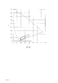
圖2係將自發光元件封裝體10出射之光(入射至綠色量子點含有層20之光)之較佳之色度範圍表示於色度座標上所成之圖。自發光元件封裝體10出射之光之色度較佳為圖2中以虛線表示之四邊形之範圍(即,於CIE1931色度圖之xy色度座標系統中,將(0.4066、0.1532)、(0.3858、0.1848)、(0.1866、0.0983)及(0.1706、0.0157)4點連接而形成之四邊形之範圍)內。
自發光元件封裝體10出射之光之色度更佳為圖2中以實線表示之四邊形之範圍(即,於CIE1931色度圖之xy色度座標系統中,將(0.19、0.099779)、(0.19、0.027013)、(0.3、0.09111)及(0.3、0.14753)4點連接而形成之四邊形之範圍)內。
藉由將色度設為此種範圍,於與綠色量子點含有層20一起使用時,可獲得作為背光裝置而較佳之色調。
將實際製作出射光之色度處於此種範圍內之發光元件封裝體10並測定發光光譜之例表示如下。
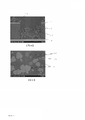
圖3A係表示所製作之發光元件封裝體10之截面之一部分之SEM圖像,圖3B係圖3A之A部之放大SEM圖像,圖3C係圖3A之B部之放大SEM圖像,圖3D係圖3A之C部之放大SEM圖像,圖3E係圖3B之D部之放大SEM圖像。
使用了具備俯視時角部帶有弧度之大致四邊形之空腔、並具有縱4 mm、橫1.4 mm、高0.6 mm之外形尺寸之樹脂封裝體3。樹脂封裝體3於空腔之底面具有一對引線5,引線5於表面具有鍍敷層15。於一對引線5之一個上配置有具有透光性基板13及半導體層11之發光元件1。將發光元件1與一對引線利用金屬線進行電性連接。發光元件1發出之光於435 nm~465 nm之間具有發光強度之峰。
密封樹脂12係將分散有紅色螢光體14及填料16之矽酮樹脂配置於樹脂封裝體3之空腔內,並使紅色螢光體14及填料16離心沈澱而形成。作為紅色螢光體14,使用了KSF螢光體(K
2SiF
6:Mn
4+)。作為填料16,使用了二氧化矽填料及奈米二氧化矽填料。密封樹脂12相對於矽酮樹脂100重量份,含有KSF螢光體約17重量份、二氧化矽填料約5重量份、及奈米二氧化矽填料約0.4重量份。
如圖3C所示,發光元件1之側面上部未被紅色螢光體14及填料16覆蓋。
圖4係所得之發光元件封裝體10之發光光譜。發光元件1主要發出430 nm~480 nm之波長之光,紅色螢光體14主要發出600 nm~660 nm之波長之光。於447 nm具有顯示出發光元件1之發光強度之最大值之第1峰值波長,於631 nm具有顯示出紅色螢光體14之發光強度之最大值之第2峰值波長。第1峰值波長處之發光強度與第2峰值波長處之發光強度之比為第1:第2=100:67。
CIE1931中之色度座標之值為x=0.216,y=0.054。
繼而,示出發光裝置100之各要素之詳細情況。
1)發光元件
發光元件1只要發出藍色光(發光峰值波長為435~465 nm之範圍內),則可為已知之任意之發光元件,亦可為藍色LED晶片。發光元件1可具備半導體積層體,較佳為具備氮化物半導體積層體。半導體積層體(較佳為氮化物半導體積層體)可依序具有第1半導體層(例如n型半導體層)、發光層及第2半導體層(例如p型半導體層)。
作為較佳之氮化物半導體材料,具體而言,可使用In
XAl
YGa
1-X-YN(0≦X、0≦Y、X+Y≦1)。各層之膜厚及層結構可使用該領域中已知者。
2)紅色螢光體
紅色螢光體14係KSF螢光體及MGF螢光體之至少一者。KSF螢光體及MGF螢光體幾乎不吸收綠色光,因而具有幾乎不產生2次吸收之優點。又,其特徵在於,發光峰之半值寬為35 nm以下,較佳為較小為10 nm以下。以下,對KSF螢光體及MGF螢光體進行詳述。
(KSF螢光體)
KSF螢光體係其發光波長之峰值處於610~650 nm之範圍之紅色螢光體。其組成係以下述通式(1)表示。
A
2[M
1-aMn
4+ aF
6] (1)
(式中,A係選自由K
+、Li
+、Na
+、Rb
+、Cs
+及NH
4+所組成之群中之至少1種,M係選自由第4族元素及第14族元素所組成之群中之至少1種元素,a滿足0<a<0.2)
KSF螢光體之發光峰之半值寬為10 nm以下。
再者,對於該KSF螢光體,可參照本案申請人先前申請過專利之日本專利特願2014-122887號。
對KSF螢光體之製造方法之一例進行說明。首先,以達到所需之組成比之方式稱量KHF
2、K
2MnF
6。將稱量出之KHF
2溶解於HF水溶液中,製備溶液A。又,將稱量出之K
2MnF
6溶解於HF水溶液中而製備溶液B。進而,以達到所需之組成比之方式製備含有H
2SiF
6之水溶液,作為含有H
2SiF
6之溶液C。此後,一面於室溫下攪拌溶液A,一面分別滴加溶液B及溶液C。對所得之沈澱物進行固液分離後,進行乙醇清洗並加以乾燥,藉此可得到KSF螢光體。
(MGF螢光體)
MGF係發出深紅色之螢光之紅色螢光體。即,其係發光波長之峰值為比KSF螢光體長波長側之650 nm以上、經Mn
4+活化之螢光體。作為組成式之一例,以3.5MgO・0.5MgF
2・GeO
2:Mn
4+表示。MGF螢光體之半值寬為15 nm以上且35 nm以下。
對於MGF螢光體,可將其組成中之MgO之Mg元素之一部分用Li、Na、K、Sc、Y、La、Ce、Pr、Nd、Pm、Sm、Eu、Gd、Tb、Dy、Ho、Er、Tm、Yb、Lu、V、Nb、Ta、Cr、Mo、W等其他元素置換,又,亦可將GeO
2中之Ge元素之一部分置換為B、Al、Ga、In等其他元素,藉此來提高發光效率。較佳為將Mg及Ge兩種元素分別置換為Sc及Ga兩種元素,藉此可更進一步提高被稱作深紅色之600~670 nm之波長區域之光之發光強度。
MGF螢光體係以下述通式(2)表示之螢光體。
(x-a)MgO・(a/2)Sc
2O
3・yMgF
2・cCaF
2・(1-b)GeO
2・(b/2)Mt
2O
3:zMn
4+(2)
(式中,x、y、z、a、b、c滿足2.0≦x≦4.0、0<y<1.5、0<z<0.05、0≦a<0.5、0<b<0.5、0≦c<1.5、y+c<1.5,Mt係選自Al、Ga、In中之至少1種)
藉由在通式(2)中,設為0.05≦a≦0.3、0.05≦b<0.3,可進一步提高發出之紅色光之亮度。再者,對於MGF螢光體,可參照本案申請人先前申請過專利之日本專利特願2014-113515號。
對本發明之實施形態之MGF螢光體之製造方法之一例進行說明。首先,作為原料,以成為所需之組成比之方式稱量MgO、MgF
2、Sc
2O
3、GeO
2、Ga
2O
3、MnCO
3。混合該等原料後,將該混合之原料填充至坩堝中,然後於大氣中以1000~1300℃煅燒,藉此可得到MGF螢光體。
發光元件之峰值波長處之發光強度與紅色螢光體之峰值波長處之發光強度之比較佳為第1:第2=100:55~70。
3)綠色量子點
綠色量子點24可列舉半導體材料、例如II-VI族、III-V族或IV-VI族等之化合物半導體,更具體而言,可列舉CdSe、核殼型之CdS
xSe
1-x/ZnS、GaP等之奈米尺寸之粒子。綠色量子點24例如具有1~20 nm之粒徑(平均粒徑)。綠色量子點24例如發出其發光波長之峰值處於510~560 nm之範圍之綠色光。綠色量子點24之發光峰之半值寬為40 nm以下,較佳為小至30 nm以下。
綠色量子點亦可利用例如PMMA(聚甲基丙烯酸甲酯)之類之樹脂等進行表面修飾或穩定化。於該情形時,所謂粒徑,係指不包括為了表面修飾及穩定化而附加之樹脂等部分之、包含半導體材料之核部分之粒徑。
4)透光性材料
透光性材料22可使藍色光、綠色光及紅色光透過。透光性材料使自發光元件1出射並入射至透光性材料22之光中較佳為60%以上、更佳為70%以上、80%以上或90%以上透過。
作為較佳之透光性材料22,可例示:高應變點玻璃、鈉鈣玻璃(Na
2O・CaO・SiO
2)、硼矽酸玻璃(Na
2O・B
2O
3・SiO
2)、鎂橄欖石(2MgO・SiO
2)、鉛玻璃(Na
2O・PbO・SiO
2)、無鹼玻璃。或者可列舉由聚甲基丙烯酸甲酯(PMMA)或聚乙烯醇(PVA)、聚乙烯基苯酚(PVP)、聚醚碸(PES)、聚醯亞胺、聚碳酸酯(PC)、聚對苯二甲酸乙二酯(PET)、聚苯乙烯(PS)、聚萘二甲酸乙二酯(PEN)、環狀非晶質聚烯烴、多官能丙烯酸酯、多官能聚烯烴、不飽和聚酯、環氧樹脂、矽酮樹脂所例示之有機聚合物(具有由高分子材料構成之具有可撓性之塑膠膜或塑膠片材、塑膠基板等高分子材料之形態)。
5)密封樹脂
密封樹脂12可使藍色光及紅色光透過,較佳為亦可使綠色光透過。透光性材料使自發光元件1出射並入射至透光性材料22之光中較佳為60%以上、更佳為70%以上、80%以上或90%以上透過。
作為較佳之密封樹脂12,可列舉矽酮樹脂、矽酮改性樹脂、環氧樹脂、環氧改性樹脂、酚系樹脂、聚碳酸酯樹脂、丙烯酸系樹脂、TPX樹脂、聚降烯樹脂或含有1種以上之該等樹脂之混成樹脂等樹脂。其中較佳為矽酮樹脂或環氧樹脂,特別是耐光性、耐熱性優異之矽酮樹脂更佳。
6)樹脂封裝體
樹脂封裝體3可由任意種類之樹脂構成。作為較佳之樹脂,可例示包含芳香族聚醯胺樹脂、聚酯樹脂、液晶樹脂之至少1種以上之熱塑性樹脂、或環氧樹脂、改性環氧樹脂、酚系樹脂、矽酮樹脂、改性矽酮樹脂、混成樹脂、丙烯酸酯樹脂、胺基甲酸酯樹脂、及含有至少1種以上之該等樹脂之熱硬化性樹脂等。樹脂封裝體3較佳為包含白色之樹脂。其原因在於,可更多地反射於密封樹脂12之內部前進之光中到達樹脂封裝體3之光。
2.實施形態2
圖5係實施形態2之發光裝置100A之概略剖視圖。上述之發光裝置100中,密封樹脂12含有紅色螢光體14。然而,於發光裝置100A中,係透光性材料22含有紅色螢光體14,代替密封樹脂12含有紅色螢光體14。因而,於透光性材料22之內部配置有紅色螢光體14及綠色量子點24,藉此相對於發光元件1,可使紅色螢光體14及綠色量子點24位於大致相同之距離。
發光元件封裝體10A除了密封樹脂12不含有紅色螢光體14以外,可具有與實施形態1之發光元件封裝體10相同之構成。又,綠色量子點含有層20A除了在綠色量子點24之外亦含有紅色螢光體14以外,可具有與實施形態1之綠色量子點含有層20相同之構成。
如以上說明所示,實施形態1之發光裝置100中,相對於發光元件1,紅色螢光體14位於比綠色量子點24近之距離,實施形態2之發光裝置100A中,相對於發光元件1,紅色螢光體14及綠色量子點24位於大致相同之距離。各個實施形態具有不同之優點。以下,對其優點進行說明。
1)發光裝置100之優點
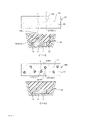
圖6A、6B係用於說明發光裝置100之優點之模式剖視圖,圖6A係表示將紅色螢光體14配置於密封樹脂12之內部之實施形態之模式剖視圖,圖6B係表示將紅色螢光體14配置於透光性材料22之內部之實施形態之模式剖視圖。如上所述,紅色螢光體14之粒徑為20~50 μm,綠色量子點24之粒徑為2~10 nm,於粒徑方面有兩位數左右之較大差異。
圖6A、3B係以更加明確地顯示基於該粒徑之差異之發光裝置100之優點為目的之模式圖,與圖1及圖5相比,更加明確地顯示出紅色螢光體14與綠色量子點24之粒徑之差異。
圖6A之符號114模式性地表示作為複數個紅色螢光體14中之1個之紅色螢光體14X發出之紅色光(一部分),符號124模式性地表示作為複數個綠色量子點24中之1個之綠色量子點24X發出之綠色光(一部分)。同樣地,圖6B之符號114A模式性地表示作為複數個紅色螢光體14中之1個之紅色螢光體14Y發出之紅色光(一部分),符號124A模式性地表示作為複數個綠色量子點24中之1個之綠色量子點24Y發出之綠色光(一部分)。
如圖6B所示,若於透光性材料22內配置粒徑較大之紅色螢光體14,則自綠色量子點24Y發出之綠色光124A由存在於其前進路線中之紅色螢光體14散射而不會到達綠色量子點含有層20A之上表面(圖6B中,紅色光114A自綠色量子點含有層20A之上表面向外側出射,但綠色光124A未到達綠色量子點含有層20A之上表面)。因粒徑較大之紅色螢光體14存在於綠色量子點含有層20A中而使綠色光之一部分中產生此種散射,該情況可能成為發光效率略為降低之要因。
與此相對,如圖6A所示,綠色量子點含有層20不含有粒徑較大之紅色螢光體14,除去透光性材料22以外,僅含有綠色量子點24。並且,於綠色量子點含有層20中前進之綠色光由粒徑非常小之綠色量子點24散射之可能性相當低(圖6A中,紅色光114及綠色光124自綠色量子點含有層20之上表面向外側出射)。因此,可獲得更高之發光效率。
2)發光裝置100A之優點
發光裝置100A之綠色量子點含有層20A如上所述含有紅色螢光體14及綠色量子點24兩者。雖然紅色螢光體14與綠色量子點24相比由熱引起之劣化較少,但藉由採取此種構成,對於紅色螢光體14而言亦可抑制發光元件1之發熱傳遞,從而可更加確實地抑制紅色螢光體14之劣化。
又,由於將紅色螢光體14及綠色量子點24配置於透光性材料22之內部,因此配置波長轉換材料時只要利用透光性材料22即可,無需於密封樹脂12中配置紅色螢光體14,因此製造步驟變得簡便。
再者,如上所述,發光裝置100A中,綠色量子點含有層20A之透光性材料22含有紅色螢光體14,發光元件封裝體10A之密封樹脂12不含有紅色螢光體14,亦可綠色量子點含有層20A之透光性材料22及發光元件封裝體10A之密封樹脂12兩者含有紅色螢光體14。
3.實施形態3
圖7係表示使用了實施形態3之發光裝置100B之液晶顯示器200之概略剖視圖。發光裝置100B包含發光元件封裝體10、綠色量子點含有層20、及配置於發光元件封裝體10與綠色量子點含有層20之間之導光板52。
圖7所示之實施形態中,於發光元件封裝體10之密封樹脂12與綠色量子點含有層20之間配置有導光板52。更詳細而言,密封樹脂12係與導光板52之1個側面對向而配置,綠色量子點含有層20係與導光板52之上表面對向而配置。圖7所示之實施形態中,發光元件封裝體10為頂視型,但並非限定於此,亦可具有上述側視型等其他形態。
發光裝置100B可以使自發光元件封裝體10入射至導光板52之光中到達導光板52之下表面之光向上方反射,並朝向導光板52之上表面之方式,於導光板52之下表面上具備反射板(reflector)51。
於圖7所示之實施形態中,發光元件封裝體10遠離導光板52而配置,但並不限定於此,例如可藉由使密封樹脂12或樹脂封裝體3與導光板52之側面接觸等,而使發光元件封裝體10與導光板52接觸。
綠色量子點含有層20可與導光板52之上表面接觸而配置,又,亦可遠離導光板52而配置。
於綠色量子點含有層20上配置有下部偏光膜53A。於下部偏光膜53A上配置有液晶單元54,於液晶單元54上配置有彩色濾光片陣列55。彩色濾光片陣列55例如具備如紅色彩色濾光片部55A、綠色彩色濾光片部55B及藍色彩色濾光片部55C般僅使特定顏色之光透過的對應於不同顏色之複數種彩色濾光片部。於彩色濾光片陣列55上配置有上部偏光膜53B。
繼而,對液晶顯示器200之動作進行說明。
發光元件1發出之藍色光之一部分自密封樹脂12出射。又,發光元件1發出之藍色光之一部分由配置於密封樹脂12內之紅色螢光體14吸收,自紅色螢光體14發出紅色光,該紅色光自密封樹脂12出射。即,自發光元件封裝體10出射藍色光與紅色光混合而成之紫色光,該紫色光(藍色光+紅色光)經由導光板52進入至綠色量子點含有層20。進入至綠色量子點含有層20之藍色光之一部分由綠色量子點24吸收,綠色量子點24發出綠色光。其結果,自綠色量子點含有層20之上表面出射藍色光、綠色光及紅色光混合而成之白色光,該白色光進入至下部偏光膜53A。進入至下部偏光膜53A之白色光(藍色光+綠色光+紅色光)之一部分通過下部偏光膜53A,進入至液晶單元54。進入至液晶單元54之白色光之一部分通過液晶單元54,到達彩色濾光片陣列55。
到達彩色濾光片陣列55之藍色光、綠色光及紅色光分別可通過對應之彩色濾光片部。例如,紅色光通過紅色彩色濾光片部55A,綠色光通過綠色彩色濾光片部55B,藍色光通過藍色彩色濾光片部55C。通過彩色濾光片陣列55之藍色光、綠色光及紅色光各自之一部分通過上部偏光膜53B。藉此,液晶顯示器200可顯示出所需之圖像。
如上所述,紅色螢光體14發出之紅色光及綠色量子點24發出之綠色光之發光峰之半值寬較窄,因此色純度較高。又,由於更多之光可通過紅色彩色濾光片部55A及綠色彩色濾光片部55B,因此可提高效率。
Hereinafter, embodiments of the present invention will be described with reference to the drawings. However, it should be noted that the embodiments described below are for embodying the technical idea of the present invention, and are not intended to limit the technical scope of the present invention. The configuration described in one embodiment can be applied to other embodiments unless otherwise specified. In the following description, terms indicating specific directions or positions (such as "up", "down", "right", "left" and other terms including these terms) are used as needed, but the use of such terms It is to facilitate the understanding of the invention with reference to the drawings, and is not intended to limit the technical scope of the present invention by the meanings of these terms. It should be noted that the sizes, positional relationships, and the like of members shown in the drawings are sometimes exaggerated for the sake of clarity. In addition, the parts with the same symbols shown in a plurality of drawings represent the same parts or members. Furthermore, components represented by symbols including numbers and letters, such as the symbol "10A", may have the same numbers as symbols such as "10" without letters unless otherwise specified. Elements and elements denoted by symbols with the same numerals and different letters are of the same composition. The inventors of the present invention have conducted intensive research and found that, by using at least one of KSF phosphor and MGF phosphor as a red phosphor instead of using red quantum dots, it is possible to provide green quantum dots with high luminescence Efficient light-emitting device. The KSF phosphor and the MGF phosphor, which will be described in detail later, absorb blue light emitted by the light-emitting element and emit red light, but hardly absorb the green light emitted by the green quantum dots. That is, secondary absorption is not caused. Therefore, the light-emitting device of the embodiment of the present invention has high light-emitting efficiency. In addition, the half-value widths of the peaks in the emission spectra of the KSF phosphor and the MGF phosphor are as narrow as about 10 to 20 nm. Therefore, even in the case of passing through a color filter that transmits substantially the entire region of the wavelength region of red, red with a narrower half-value width can be obtained, and thus red light with high color purity can be obtained. In addition, in this specification, the so-called "quantum dot" refers to a wavelength conversion material utilizing the quantum size effect of semiconductor fine particles (semiconductor nanoparticles). It is known that semiconductor fine particles exhibit a quantum size effect when the particle diameter is, for example, several tens of nanometers or less. The quantum size effect refers to the phenomenon that the energy bands of the valence electron band and the conduction band, which are considered to be continuous in the bulk particle, become discrete when the particle size is set to the nanometer size, and the band gap energy is determined according to the varies with particle size. Such semiconductor nanoparticles with quantum size effect can absorb light and emit light corresponding to its band gap energy, so it can be used as a wavelength conversion material in light-emitting devices. Hereinafter, the light-emitting devices of several embodiments of the present invention will be described in detail. 1. Embodiment 1 FIG. 1 is a schematic cross-sectional view of a light-emitting device 100 according to Embodiment 1. As shown in FIG. The light-emitting device 100 includes: a light-emitting element 1 that emits blue light; green quantum dots 24 that absorb part of the blue light emitted by the light-emitting element 1 and emit green light; and a red phosphor 14 that absorbs the blue light emitted by the light-emitting element 1 part of the color light and emits red light. The red phosphor 14 is at least one of the KSF phosphor and the MGF phosphor described in detail later. In the light-emitting device of the present invention, the positional relationship of the red phosphors 14 and the green quantum dots 24 with respect to the light-emitting element 1 is not particularly limited. That is, either (1) the red phosphors 14 may be located at a closer distance than the green quantum dots 24 with respect to the light-emitting element 1, or (2) the red phosphors 14 may be located at a closer distance than the green quantum dots 24 with respect to the light-emitting element 1 Further, (3) as shown in Embodiment 2 to be described later, the red phosphor 14 and the green quantum dot 24 may be located at substantially the same distance with respect to the light-emitting element 1 . In Embodiment 1, with respect to the light-emitting element 1 , the red phosphors 14 are located at a shorter distance than the green quantum dots 24 . The light-emitting device 100 includes the light-emitting element package 10 . The light emitting element package 10 has: a resin package 3 having a bottom surface, a side wall, and a cavity surrounded by the bottom surface and the side wall with an upper opening; the light emitting element 1 is disposed on the bottom surface of the cavity of the resin package 3; and a sealing resin 12 , which is filled in the cavity of the resin package 3 . The positive and negative electrodes of the light-emitting element 1 are connected to an external power source through conductive means such as metal wires, metal bumps, and plated films, for example, and emit blue light by supplying current (electric power) from the external power source. A lead wire may also be arranged on the bottom surface of the cavity of the resin package 3, and the light-emitting element 1 may be arranged on the lead wire. When a lead wire is used, the lead wire can be connected to the negative electrode and/or the positive electrode of the light-emitting element with a metal wire, and the light-emitting element 1 can be connected to an external power source through the lead wire. In addition, it is also possible to perform flip chip connection using solder or the like without using a metal wire. Moreover, the lead wire may have a plating layer on the surface as needed. The sealing resin 12 covers the periphery of the light-emitting element 1 (in the embodiment shown in FIG. 1 , the upper surface and the side surfaces excluding the bottom surface of the light-emitting element 1 ). The sealing resin 12 contains the red phosphor 14 . That is, the red phosphors 14 are dispersed and arranged inside the sealing resin 12 . Furthermore, in the embodiment shown in FIG. 1, the red phosphors 14 are uniformly dispersed in the sealing resin 12, but the form of the dispersed arrangement of the red phosphors is not limited to this. The red phosphors 14 can be arranged in a higher density in a part of the sealing resin 12 , for example, in a high density near the light-emitting element 1 . As such an arrangement, there is a so-called precipitation arrangement, that is, the dispersion density of the red phosphor is smaller at the upper part of the sealing resin and higher at the bottom of the sealing resin 12 (including just above the light-emitting element 1 ). The precipitation configuration can be formed, for example, by filling the cavity of the resin package 3 with the sealing resin 12 before curing in which the red phosphors 14 are uniformly dispersed, and then placing the sealing resin 12 in the uncured state. When left in this state for a certain period of time, the red phosphor 14 in the sealing resin 12 moves due to gravity, and when the red phosphor 14 is distributed on the bottom of the sealing resin 12 and becomes higher, the sealing resin 12 is hardened. It can also be precipitated by centrifugal force. Furthermore, in addition to the red phosphor 14 , a filler may also be arranged inside the sealing resin 12 . The light emitting element package 10 emits blue light and red light with its upper surface serving as an exit surface. More specifically, a part of the blue light emitted from the light-emitting element 1 passes through the sealing resin 12 and is emitted to the outside from the upper surface of the sealing resin 12 . Part of the blue light emitted from the light-emitting element package 10 may be reflected from the side and/or bottom surface of the resin package 3 when traveling inside the sealing resin 12 , and then emitted from the upper surface of the sealing resin 12 . In addition, the other part of the blue light emitted from the light-emitting element 1 is absorbed by the red phosphor 14 while traveling inside the sealing resin 12 , and the red phosphor 14 emits red light. After that, the red light emitted from the red phosphor 14 passes through the sealing resin 12 and is emitted from the upper surface of the sealing resin 12 to the outside. Part of the red light emitted by the red phosphors 14 can also be emitted from the upper surface of the sealing resin 12 after being reflected by the side and/or bottom surface of the resin package 3 when traveling inside the sealing resin 12 . On the outer side of the sealing resin 12 , that is, in FIG. 1 , the green quantum dot-containing layer 20 is arranged on the upper part of the sealing resin 12 (or the resin package 3 ). The green quantum dot-containing layer 20 includes a light-transmitting material 22 and green quantum dots 24 . That is, the green quantum dots 24 are dispersed and arranged in the translucent material 22 . The green quantum dot containing layer 20 may have any shape. One of the preferred forms is sheet (or film) as shown in FIG. 1 . This is because the thickness of the green quantum dot-containing layer 20 can be made uniform, and color unevenness can be suppressed. With such a configuration, in the light-emitting device 100 , the red phosphors 14 are located at a shorter distance than the green quantum dots 24 with respect to the light-emitting element 1 . By arranging KSF phosphor or MGF phosphor with a larger particle size (or diameter) such as 20-50 μm in the vicinity of the light-emitting element, and making the particle size (or diameter) such as 2-10 nm green The quantum dots 24 are disposed near the light-emitting element 1 to suppress scattering of light, particularly, the scattering of green light caused by the red phosphor 14 . As a result, the extraction efficiency of light (ie, luminous efficiency) can be further improved. The improvement of the extraction efficiency of this light will be described in detail after the configuration of the second embodiment to be described later. Most of the red light emitted from the upper surface of the light-emitting element package 10 enters the interior from the lower surface of the green quantum dot containing layer 20 , and passes through the light-transmitting material 22 of the green quantum dot containing layer 20 , then passes through the green quantum dot containing layer 20 . 20 The upper surface is projected to the outside. Most of the blue light emitted from the upper surface of the light-emitting element package 10 enters the interior from the lower surface of the green quantum dot containing layer 20 . Part of the blue light entering the interior from the lower surface of the green quantum dots containing layer 20 is emitted to the outside from the upper surface of the green quantum dots containing layer 20 after passing through the translucent material 22 of the green quantum dots containing layer 20 . Another part of the blue light entering the interior from the lower surface of the green quantum dot containing layer 20 is absorbed by the green quantum dots 24, and the green quantum dots 24 emit green light. Most of the green light emitted from the green quantum dots 24 travels inside the light-transmitting material 22 and exits from the upper surface of the green quantum dot-containing layer 20 to the outside. As a result, on the outer side of the upper surface of the green quantum dot-containing layer 20 , blue light, red light, and green light are mixed, and white light can be obtained. Furthermore, part of the green light emitted by the green quantum dots 24 goes downward, exits from the lower surface of the green quantum dot containing layer 20 , and enters the sealing resin 12 from the upper surface of the light-emitting element package 10 . However, the red phosphor 14, which is at least one of the KSF phosphor and the MGF phosphor, hardly absorbs green light. Therefore, for example, green light such as the following, after being reflected by the inner surface of the resin package 3, exits from the upper surface of the light-emitting element package 10, enters from the lower surface of the green quantum dot containing layer 20, and emerges from the green quantum dot-containing layer 20. The quantum dot containing layer 20 emerges from the upper surface. The existence of such green light helps to improve the extraction efficiency of the light emitting device 100 . In the embodiment shown in FIG. 1 , the green quantum dot-containing layer 20 is separated from the sealing resin 12 (or the resin package 3 ). Thereby, the effect of being able to more reliably suppress the heat radiation of the light-emitting element 1 from being transferred to the green quantum dots 24 having poor heat resistance can be obtained. However, it is not limited to this, and the green quantum dot-containing layer 20 may be in contact with the sealing resin 12 (or the resin package 3 ). In this case, more light emitted from the light-emitting element package 10 enters the green quantum dot containing layer 20, which can further improve the extraction efficiency. In addition, even if the green quantum dot containing layer 20 is in contact with the sealing resin 12 (or the resin package 3 ), the light-emitting element 1 and the green quantum dots 24 are separated by a certain distance, so that the heat of the green quantum dots 24 can be suppressed. Deterioration effect. In the embodiment shown in FIG. 1 , the light-emitting element package 10 is a top-view light-emitting element package, that is, its mounting surface is the bottom surface (lower surface), and the surface on the opposite side of the light extraction surface is As a mounting surface (for example, the upper surface is used as a light extraction surface, and the lower surface is used as a mounting surface). However, the light-emitting element package 10 is not limited to this, and the light-emitting element package 10 may be configured as a so-called side view type in which the surface adjacent to the light extraction surface is used as the mounting surface. In addition, in the embodiment shown in FIG. 1, although the light emitting element package 10 containing the resin package 3 was used, it is not limited to this. Instead of the light emitting element package 10 , a so-called packageless form may be employed, that is, a phosphor layer including the red phosphor 14 is formed on the surface of the light emitting element 1 without using a resin package. FIG. 2 is a graph showing the preferred chromaticity range of the light emitted from the light-emitting element package 10 (light incident on the green quantum dot containing layer 20 ) on the chromaticity coordinates. The chromaticity of the light emitted from the light-emitting element package 10 is preferably the range of the quadrilateral represented by the dotted line in FIG. , 0.1848), (0.1866, 0.0983) and (0.1706, 0.0157) within the range of the quadrilateral formed by the connection of 4 points). The chromaticity of the light emitted from the light-emitting element package 10 is preferably the range of the quadrilateral represented by the solid line in FIG. 0.19, 0.027013), (0.3, 0.09111) and (0.3, 0.14753) are within the range of the quadrilateral formed by connecting four points). By setting the chromaticity to such a range, when used together with the green quantum dot-containing layer 20, a preferable color tone as a backlight device can be obtained. An example of actually producing the light-emitting element package 10 having the chromaticity of the emitted light within such a range and measuring the emission spectrum is shown below. FIG. 3A is a SEM image of a part of the cross section of the fabricated light-emitting element package 10 , FIG. 3B is an enlarged SEM image of part A of FIG. 3A , and FIG. 3C is an enlarged SEM image of part B of FIG. 3A . 3D is an enlarged SEM image of part C of FIG. 3A, and FIG. 3E is an enlarged SEM image of part D of FIG. 3B. A resin package 3 having an approximately quadrangular cavity with curved corners in plan view and having external dimensions of 4 mm in length, 1.4 mm in width, and 0.6 mm in height was used. The resin package 3 has a pair of leads 5 on the bottom surface of the cavity, and the leads 5 have a plated layer 15 on the surface. The light-emitting element 1 having the light-transmitting substrate 13 and the semiconductor layer 11 is arranged on one of the pair of leads 5 . The light-emitting element 1 and a pair of lead wires are electrically connected by metal wires. The light emitted from the light-emitting element 1 has a peak of luminous intensity between 435 nm and 465 nm. The sealing resin 12 is formed by disposing a silicone resin in which the red phosphor 14 and the filler 16 are dispersed in the cavity of the resin package 3 , and centrifugally precipitating the red phosphor 14 and the filler 16 . As the red phosphor 14, KSF phosphor (K 2 SiF 6 : Mn 4+ ) was used. As the filler 16, silica filler and nano silica filler were used. The sealing resin 12 contains about 17 parts by weight of KSF phosphor, about 5 parts by weight of silica filler, and about 0.4 part by weight of nano silica filler relative to 100 parts by weight of silicone resin. As shown in FIG. 3C , the upper part of the side surface of the light-emitting element 1 is not covered by the red phosphor 14 and the filler 16 . FIG. 4 shows the emission spectrum of the obtained light-emitting element package 10 . The light-emitting element 1 mainly emits light with a wavelength of 430 nm to 480 nm, and the red phosphor 14 mainly emits light with a wavelength of 600 nm to 660 nm. At 447 nm, it has a first peak wavelength showing the maximum value of the emission intensity of the light-emitting element 1, and at 631 nm, it has a second peak wavelength showing the maximum value of the emission intensity of the red phosphor 14. The ratio of the luminous intensity at the first peak wavelength to the luminous intensity at the second peak wavelength is 1st:2nd=100:67. The values of the chromaticity coordinates in CIE1931 are x=0.216, y=0.054. Next, the details of each element of the light-emitting device 100 are shown. 1) Light-emitting element The light-emitting element 1 may be any known light-emitting element or a blue LED chip as long as it emits blue light (the emission peak wavelength is in the range of 435-465 nm). The light-emitting element 1 may include a semiconductor laminate, preferably a nitride semiconductor laminate. The semiconductor laminate (preferably, a nitride semiconductor laminate) may have a first semiconductor layer (eg, an n-type semiconductor layer), a light-emitting layer, and a second semiconductor layer (eg, a p-type semiconductor layer) in this order. As a preferable nitride semiconductor material, specifically, In X Al Y Ga 1-XY N (0≦X, 0≦Y, X+Y≦1) can be used. The film thickness and layer structure of each layer can be those known in the art. 2) Red phosphor The red phosphor 14 is at least one of KSF phosphor and MGF phosphor. KSF phosphors and MGF phosphors hardly absorb green light, so there is an advantage that secondary absorption hardly occurs. Furthermore, it is characterized in that the half-value width of the emission peak is 35 nm or less, preferably 10 nm or less. Hereinafter, the KSF phosphor and the MGF phosphor will be described in detail. (KSF phosphor) The KSF phosphor system is a red phosphor whose peak emission wavelength is in the range of 610-650 nm. The composition is represented by the following general formula (1). A 2 [M 1-a Mn 4+ a F 6 ] (1) (wherein, A is at least one selected from the group consisting of K + , Li + , Na + , Rb + , Cs + and NH 4+ 1, M is at least one element selected from the group consisting of Group 4 elements and Group 14 elements, a satisfies 0<a<0.2) The half width of the emission peak of the KSF phosphor is 10 nm or less. Furthermore, for the KSF phosphor, reference may be made to Japanese Patent Application No. 2014-122887 previously filed by the applicant of the present application. An example of the production method of the KSF phosphor will be described. First, KHF 2 and K 2 MnF 6 are weighed so as to achieve a desired composition ratio. Solution A was prepared by dissolving the weighed KHF 2 in an aqueous HF solution. Moreover, the solution B was prepared by dissolving K 2 MnF 6 weighed in the HF aqueous solution. Further, an aqueous solution containing H 2 SiF 6 was prepared as a solution C containing H 2 SiF 6 so as to achieve a desired composition ratio. After that, while stirring the solution A at room temperature, the solution B and the solution C were added dropwise, respectively. The obtained precipitate is subjected to solid-liquid separation, washed with ethanol, and dried to obtain a KSF phosphor. (MGF phosphor) MGF is a red phosphor that emits deep red fluorescence. That is, the peak of the emission wavelength is 650 nm or more on the longer wavelength side than the KSF phosphor, and the phosphor is activated by Mn 4+ . As an example of the composition formula, it is represented by 3.5MgO·0.5MgF 2 ·GeO 2 : Mn 4+ . The half-value width of the MGF phosphor is 15 nm or more and 35 nm or less. For MGF phosphor, Li, Na, K, Sc, Y, La, Ce, Pr, Nd, Pm, Sm, Eu, Gd, Tb, Dy, Ho can be used as part of the Mg element of MgO in its composition. , Er, Tm, Yb, Lu, V, Nb, Ta, Cr, Mo, W and other elements are replaced, and part of the Ge elements in GeO 2 can also be replaced by B, Al, Ga, In and other elements , thereby improving the luminous efficiency. Preferably, two elements, Mg and Ge, are replaced by two elements, Sc and Ga, respectively, whereby the luminous intensity of light in the wavelength region of 600 to 670 nm, which is called deep red, can be further improved. The MGF phosphor system is a phosphor represented by the following general formula (2). (x-a)MgO・(a/2)Sc 2 O 3・yMgF 2・cCaF 2・(1-b)GeO 2・(b/2)Mt 2 O 3 : zMn 4+ (2) (wherein , x, y, z, a, b, c satisfy 2.0≦x≦4.0, 0<y<1.5, 0<z<0.05, 0≦a<0.5, 0<b<0.5, 0≦c<1.5, y+c <1.5, Mt is at least one selected from Al, Ga, and In) By setting 0.05≦a≦0.3 and 0.05≦b<0.3 in the general formula (2), the intensity of the emitted red light can be further improved. brightness. Furthermore, regarding the MGF phosphor, reference may be made to Japanese Patent Application No. 2014-113515 previously filed by the applicant of the present application. An example of the manufacturing method of the MGF fluorescent substance which concerns on embodiment of this invention is demonstrated. First, as raw materials, MgO, MgF 2 , Sc 2 O 3 , GeO 2 , Ga 2 O 3 , and MnCO 3 are weighed so as to have a desired composition ratio. After mixing these raw materials, a crucible is filled with the mixed raw materials, and then calcined at 1000-1300° C. in the air, whereby an MGF phosphor can be obtained. The ratio of the luminous intensity at the peak wavelength of the light-emitting element and the luminous intensity at the peak wavelength of the red phosphor is preferably 1st:2nd=100:55-70. 3) Green quantum dots The green quantum dots 24 include semiconductor materials, such as compound semiconductors of II-VI, III-V or IV-VI groups, and more specifically, CdSe, core-shell CdS x Se Nano-sized particles of 1-x /ZnS, GaP, etc. The green quantum dots 24 have, for example, a particle size (average particle size) of 1 to 20 nm. The green quantum dots 24 emit, for example, green light whose emission wavelength peak is in the range of 510 to 560 nm. The half-value width of the emission peak of the green quantum dots 24 is 40 nm or less, preferably as small as 30 nm or less. Green quantum dots can also be surface-modified or stabilized with resins such as PMMA (polymethyl methacrylate). In this case, the particle diameter refers to the particle diameter of the core part including the semiconductor material, excluding parts such as resins added for surface modification and stabilization. 4) Translucent material The translucent material 22 can transmit blue light, green light and red light. The light-transmitting material transmits preferably 60% or more, more preferably 70% or more, 80% or more, or 90% or more of the light emitted from the light-emitting element 1 and incident on the light-transmitting material 22 . As a preferable translucent material 22, high strain point glass, soda lime glass (Na 2 O·CaO·SiO 2 ), borosilicate glass (Na 2 O·B 2 O 3 ·SiO 2 ), magnesium Olivine (2MgO・SiO 2 ), lead glass (Na 2 O・PbO・SiO 2 ), alkali-free glass. Alternatively, polymethyl methacrylate (PMMA) or polyvinyl alcohol (PVA), polyvinyl phenol (PVP), polyether sulfone (PES), polyimide, polycarbonate (PC), polypara Ethylene phthalate (PET), polystyrene (PS), polyethylene naphthalate (PEN), cyclic amorphous polyolefin, multifunctional acrylate, multifunctional polyolefin, unsaturated polyester , Organic polymers exemplified by epoxy resins and silicone resins (having the form of polymer materials such as flexible plastic films, plastic sheets, and plastic substrates composed of polymer materials). 5) Sealing resin The sealing resin 12 can transmit blue light and red light, and preferably also transmit green light. The light-transmitting material transmits preferably 60% or more, more preferably 70% or more, 80% or more, or 90% or more of the light emitted from the light-emitting element 1 and incident on the light-transmitting material 22 . As the preferable sealing resin 12, silicone resin, silicone modified resin, epoxy resin, epoxy modified resin, phenolic resin, polycarbonate resin, acrylic resin, TPX resin, polyolefin resin can be mentioned. Resins such as olefin resins or mixed resins containing one or more of these resins. Among them, silicone resin or epoxy resin is preferable, and silicone resin with excellent light resistance and heat resistance is more preferable. 6) Resin package The resin package 3 may be composed of any kind of resin. Preferred resins include thermoplastic resins containing at least one of aromatic polyamide resins, polyester resins, and liquid crystal resins, or epoxy resins, modified epoxy resins, phenolic resins, silicone resins, modified Silicone resins, hybrid resins, acrylate resins, urethane resins, and thermosetting resins containing at least one of these resins. The resin package 3 preferably contains white resin. The reason for this is that more light reaching the resin package 3 can be reflected in the light traveling inside the sealing resin 12 . 2. Embodiment 2 FIG. 5 is a schematic cross-sectional view of a light-emitting device 100A according to Embodiment 2. As shown in FIG. In the light-emitting device 100 described above, the sealing resin 12 contains the red phosphor 14 . However, in the light-emitting device 100A, the translucent material 22 contains the red phosphor 14 , and the red phosphor 14 is contained in place of the sealing resin 12 . Therefore, the red phosphors 14 and the green quantum dots 24 are arranged inside the translucent material 22 , and the red phosphors 14 and the green quantum dots 24 can be located at substantially the same distance from the light-emitting element 1 . The light-emitting element package 10A may have the same configuration as the light-emitting element package 10 of Embodiment 1 except that the sealing resin 12 does not contain the red phosphor 14 . Further, the green quantum dot-containing layer 20A may have the same configuration as that of the green quantum dot-containing layer 20 of Embodiment 1, except that the red phosphor 14 is contained in addition to the green quantum dots 24 . As described above, in the light-emitting device 100 of the first embodiment, the red phosphor 14 is located at a distance closer to the light-emitting element 1 than the green quantum dots 24 , and in the light-emitting device 100A of the second embodiment, with respect to the light-emitting element 1 , the red phosphors 14 and the green quantum dots 24 are located at approximately the same distance. Each embodiment has different advantages. Hereinafter, the advantages will be described. 1) Advantages of the light-emitting device 100 FIGS. 6A and 6B are schematic cross-sectional views for explaining the advantages of the light-emitting device 100. FIG. 6A is a schematic cross-sectional view showing an embodiment in which the red phosphor 14 is disposed inside the sealing resin 12, and FIG. 6B It is a schematic cross-sectional view showing an embodiment in which the red phosphor 14 is arranged inside the translucent material 22 . As mentioned above, the particle size of the red phosphor 14 is 20-50 μm, and the particle size of the green quantum dots 24 is 2-10 nm, and there is a large difference in particle size of about two digits. FIGS. 6A and 3B are schematic diagrams for the purpose of more clearly showing the advantages of the light-emitting device 100 based on the difference in particle size. Compared with FIGS. 1 and 5 , the red phosphors 14 and the green quantum particles are more clearly shown. Difference in particle size at point 24. Reference numeral 114 in FIG. 6A schematically represents the red light (a part) emitted by the red phosphor 14X which is one of the plurality of red phosphors 14 , and reference numeral 124 schematically represents the red light emitted as one of the plurality of green quantum dots 24 . Green light (part) emitted by 1 green quantum dot 24X. Similarly, reference numeral 114A in FIG. 6B schematically represents red light (a part) emitted by the red phosphor 14Y, which is one of the plurality of red phosphors 14 , and reference numeral 124A schematically represents a plurality of green quantum dots. Green light (a part) emitted by the green quantum dot 24Y of one of the 24. As shown in FIG. 6B , if the red phosphor 14 with a larger particle size is arranged in the light-transmitting material 22 , the green light 124A emitted from the green quantum dots 24Y is emitted by the red phosphor 14 existing in its advancing path. Scattered without reaching the upper surface of the green quantum dot-containing layer 20A (in FIG. 6B, the red light 114A exits from the upper surface of the green quantum dot-containing layer 20A to the outside, but the green light 124A does not reach the green quantum dot-containing layer 20A. surface). Such scattering occurs in part of the green light due to the presence of the red phosphor 14 with a large particle size in the green quantum dot-containing layer 20A, which may be a cause of a slight decrease in luminous efficiency. In contrast, as shown in FIG. 6A , the green quantum dot-containing layer 20 does not contain the red phosphor 14 having a large particle size, and only contains the green quantum dots 24 except for the light-transmitting material 22 . Also, the green light traveling in the green quantum dot-containing layer 20 is less likely to be scattered by the green quantum dots 24 with very small particle size (in FIG. The upper surface exits outward). Therefore, higher luminous efficiency can be obtained. 2) Advantages of the light-emitting device 100A The green quantum dot-containing layer 20A of the light-emitting device 100A contains both the red phosphor 14 and the green quantum dots 24 as described above. Although the red phosphor 14 is less degraded by heat than the green quantum dots 24, by adopting such a configuration, the heat transfer of the light-emitting element 1 can be suppressed for the red phosphor 14, so that more Deterioration of the red phosphor 14 is surely suppressed. Furthermore, since the red phosphors 14 and the green quantum dots 24 are arranged inside the translucent material 22 , it is only necessary to use the translucent material 22 when arranging the wavelength conversion material, and it is not necessary to arrange the red phosphors in the sealing resin 12 . body 14, so the manufacturing steps are simplified. Furthermore, as described above, in the light-emitting device 100A, the light-transmitting material 22 of the green quantum dot-containing layer 20A contains the red phosphor 14, and the sealing resin 12 of the light-emitting element package 10A does not contain the red phosphor 14. Both the translucent material 22 of the green quantum dot-containing layer 20A and the sealing resin 12 of the light-emitting element package 10A contain the red phosphor 14 . 3. Embodiment 3 FIG. 7 is a schematic cross-sectional view showing a liquid crystal display 200 using the light-emitting device 100B of Embodiment 3. As shown in FIG. The light emitting device 100B includes a light emitting element package 10 , a green quantum dot containing layer 20 , and a light guide plate 52 disposed between the light emitting element package 10 and the green quantum dot containing layer 20 . In the embodiment shown in FIG. 7 , a light guide plate 52 is arranged between the sealing resin 12 of the light-emitting element package 10 and the green quantum dot-containing layer 20 . More specifically, the sealing resin 12 is arranged to face one side surface of the light guide plate 52 , and the green quantum dot-containing layer 20 is arranged to face the upper surface of the light guide plate 52 . In the embodiment shown in FIG. 7 , the light-emitting element package 10 is a top view type, but it is not limited to this, and may have other forms such as the above-mentioned side view type. The light emitting device 100B can make the light incident from the light emitting element package 10 to the light guide plate 52 and the light reaching the lower surface of the light guide plate 52 to be reflected upward and toward the upper surface of the light guide plate 52 . A reflector 51 is provided thereon. In the embodiment shown in FIG. 7 , the light emitting element package 10 is disposed away from the light guide plate 52, but it is not limited to this. For example, the sealing resin 12 or the resin package 3 can be brought into contact with the side surface of the light guide plate 52. , and the light-emitting element package 10 is brought into contact with the light guide plate 52 . The green quantum dot-containing layer 20 may be disposed in contact with the upper surface of the light guide plate 52 , or may be disposed away from the light guide plate 52 . The lower polarizing film 53A is arranged on the green quantum dot containing layer 20 . A liquid crystal cell 54 is arranged on the lower polarizing film 53A, and a color filter array 55 is arranged on the liquid crystal cell 54 . The color filter array 55 includes, for example, a red color filter portion 55A, a green color filter portion 55B, and a blue color filter portion 55C, such as a plurality of colors corresponding to different colors that transmit only light of a specific color. filter section. The upper polarizing film 53B is arranged on the color filter array 55 . Next, the operation of the liquid crystal display 200 will be described. A part of the blue light emitted from the light-emitting element 1 is emitted from the sealing resin 12 . In addition, part of the blue light emitted from the light-emitting element 1 is absorbed by the red phosphor 14 disposed in the sealing resin 12 , and red light is emitted from the red phosphor 14 , and the red light is emitted from the sealing resin 12 . That is, violet light obtained by mixing blue light and red light is emitted from the light-emitting element package 10 , and the violet light (blue light+red light) enters the green quantum dot-containing layer 20 via the light guide plate 52 . A portion of the blue light entering the green quantum dot containing layer 20 is absorbed by the green quantum dots 24, which emit green light. As a result, white light in which blue light, green light, and red light are mixed is emitted from the upper surface of the green quantum dot-containing layer 20 , and the white light enters the lower polarizing film 53A. Part of the white light (blue light+green light+red light) entering the lower polarizing film 53A passes through the lower polarizing film 53A and enters the liquid crystal cell 54 . A portion of the white light entering the liquid crystal cell 54 passes through the liquid crystal cell 54 and reaches the color filter array 55 . The blue light, green light and red light reaching the color filter array 55 can pass through the corresponding color filter portions, respectively. For example, red light passes through the red color filter portion 55A, green light passes through the green color filter portion 55B, and blue light passes through the blue color filter portion 55C. A portion of each of the blue light, green light, and red light passing through the color filter array 55 passes through the upper polarizing film 53B. Thereby, the liquid crystal display 200 can display a desired image. As described above, the red light emitted by the red phosphor 14 and the green light emitted by the green quantum dots 24 have narrower half-value widths of emission peaks, and thus have higher color purity. In addition, since more light can pass through the red color filter portion 55A and the green color filter portion 55B, the efficiency can be improved.