RU2734452C2 - Dark current compensation - Google Patents
Dark current compensation Download PDFInfo
- Publication number
- RU2734452C2 RU2734452C2 RU2018122963A RU2018122963A RU2734452C2 RU 2734452 C2 RU2734452 C2 RU 2734452C2 RU 2018122963 A RU2018122963 A RU 2018122963A RU 2018122963 A RU2018122963 A RU 2018122963A RU 2734452 C2 RU2734452 C2 RU 2734452C2
- Authority
- RU
- Russia
- Prior art keywords
- radiation
- dark current
- pixels
- detector
- compensation
- Prior art date
Links
Images
Classifications
-
- G—PHYSICS
- G01—MEASURING; TESTING
- G01T—MEASUREMENT OF NUCLEAR OR X-RADIATION
- G01T1/00—Measuring X-radiation, gamma radiation, corpuscular radiation, or cosmic radiation
- G01T1/16—Measuring radiation intensity
- G01T1/24—Measuring radiation intensity with semiconductor detectors
-
- G—PHYSICS
- G01—MEASURING; TESTING
- G01T—MEASUREMENT OF NUCLEAR OR X-RADIATION
- G01T1/00—Measuring X-radiation, gamma radiation, corpuscular radiation, or cosmic radiation
- G01T1/16—Measuring radiation intensity
- G01T1/24—Measuring radiation intensity with semiconductor detectors
- G01T1/244—Auxiliary details, e.g. casings, cooling, damping or insulation against damage by, e.g. heat, pressure or the like
Abstract
Description
ОБЛАСТЬ ИЗОБРЕТЕНИЯFIELD OF THE INVENTION
Настоящее изобретение в целом относится к детектору излучения, содержащему матрицу пикселей, содержащую множество пикселей обнаружения для обнаружения информации об изображении. Настоящее изобретение также относится к способу обнаружения спектрального излучения и системе визуализации.The present invention generally relates to a radiation detector comprising a pixel array comprising a plurality of detection pixels for detecting image information. The present invention also relates to a spectral radiation detection method and an imaging system.
ПРЕДПОСЫЛКИ ИЗОБРЕТЕНИЯBACKGROUND OF THE INVENTION
Детекторы с энергетическим разрешением для счета фотонов основаны на материалах прямого преобразования, таких как теллурид кадмия-цинка (CdZnTe, также известный как CZT) или теллурид кадмия (CdTe). Материалы прямого преобразования представляют собой полупроводниковые соединения, которые часто имеют незначительные нежелательные явления, которые являются причиной ложной информации и/или увеличивают шум или потерю разрешения. Например, пиксель детектора может принимать некоторый заряд, предназначенный для соседнего пикселя (разделение заряда), или он может показывать ток, протекающий через полупроводниковый материал, даже когда излучение к полупроводнику (темновой ток) не испускается. Темновой ток изменяется от нескольких нА на пиксель до нескольких десятков нА на пиксель в зависимости от типа электродов (например, блокирующих или омических электродов) и удельного сопротивления датчика. Упомянутый темновой ток сильно зависит от температуры, преимущественно, как экспоненциальная функция, что в основном обусловлено увеличением тепловых равновесных плотностей электронов зоны проводимости и валентных зон с увеличением температуры.Energy-resolved photon counting detectors are based on direct conversion materials such as cadmium zinc telluride (CdZnTe, also known as CZT) or cadmium telluride (CdTe). Direct conversion materials are semiconductor compounds that often have minor undesirable effects that cause false information and / or increase noise or loss of resolution. For example, a detector pixel may receive some charge intended for an adjacent pixel (charge separation), or it may indicate a current flowing through the semiconductor material even when no radiation is emitted to the semiconductor (dark current). The dark current varies from several nA per pixel to several tens of nA per pixel, depending on the type of electrodes (for example, blocking or ohmic electrodes) and the resistivity of the sensor. The aforementioned dark current strongly depends on temperature, mainly as an exponential function, which is mainly due to an increase in the thermal equilibrium electron densities of the conduction and valence bands with increasing temperature.
В частности, CZT демонстрирует ряд нежелательных артефактов, вызываемых различными причинами, что в последние годы постоянно исправляется. Для решения проблем, связанных некоторыми из этих артефактов (например, усиления фотопроводимости), например, требуются схемы восстановления базового уровня (BLR). Такие схемы также компенсируют темновой ток и медленные колебания, вызванные изменениями температуры. Однако сами схемы BLR также вызывают ряд артефактов, связанных с высокоскоростными применениями. Как только CZT не демонстрирует избыточного тока, зависящего от каких-либо изменений (кроме фототока), использование BLR более не оправдано, учитывая дополнительные артефакты, которые он вызывает, и, в частности, учитывая, что обращение с такими несовершенствами схемы (чувствительности к индукции, наложению импульсов и т. д.) требует разработки значительно более сложных схем.In particular, CZT exhibits a number of unwanted artifacts caused by various reasons, which have been constantly corrected in recent years. Baseline recovery (BLR) circuits are required to address the problems associated with some of these artifacts (eg, photoconductivity enhancement), for example. Such circuits also compensate for dark current and slow fluctuations caused by temperature changes. However, the BLR circuits themselves also cause a number of artifacts associated with high-speed applications. Once the CZT shows no excess current dependent on any variation (other than photocurrent), the use of BLR is no longer justified given the additional artifacts it causes, and in particular given that handling such circuit imperfections (induction sensitivity , superposition of pulses, etc.) requires the development of much more complex circuits.
Приемлемое решение для вышеупомянутой зависимости темнового тока от температуры было бы весьма желательно. Изменение темнового тока вызывает смещение базовой линии, которое, в свою очередь, вызывает ошибку в оценке энергии. Хотя температура детектора обычно регулируется, диапазон изменения температуры менее +/- 1°C может не обеспечиваться. В зависимости от реализации это может привести к смещению энергии, превышающему 2 кэВ.An acceptable solution for the aforementioned temperature dependence of dark current would be highly desirable. A change in dark current causes a baseline shift, which in turn causes an error in the energy estimate. Although the detector temperature is usually adjustable, a temperature range of less than +/- 1 ° C may not be provided. Depending on the implementation, this can lead to an energy shift in excess of 2 keV.
К текущим решениям относятся, например, взятие замеров с переключением по решетке: синхронизация взятия замеров смещения базовой линии в короткий период, когда рентгеновские лучи отключены, с распределением по всей области сканирования, как это известно, например, из US 2013/0284940 A1. Это решение требует специальных усовершенствованной функциональности рентгеновской трубки и генератора.Current solutions include, for example, grating-switched sampling: synchronizing the sampling of baseline displacement in a short period, when X-rays are off, with a distribution over the entire scan area, as is known, for example, from US 2013/0284940 A1. This solution requires special advanced functionality of the X-ray tube and generator.
Другим решением может быть взятие замеров при предварительном сканировании: перед началом сканирования производится взятие замеров базовой линии и компенсируется темновой ток. Однако при длительном сканировании температура может отклониться, что вызывает ошибку оценки энергии.Another solution is to take a prescan measurement: before starting a scan, a baseline is taken and the dark current is compensated. However, with long scans, the temperature can deviate, which causes an error in the energy estimate.
Третьим потенциальным решением является связь по переменному току: это полностью исключает изменения достаточно низкой частоты. Однако для этого требуется большой развязывающий конденсатор и входной резистор смещения, несовместимый с необходимым высоким уровнем монолитной интеграции. Это также требует, чтобы BLR или держатель (BLH) базовой линии повторно установил опорный сигнал.A third potential solution is AC coupling: this completely eliminates sufficiently low frequency variations. However, this requires a large decoupling capacitor and an input bias resistor that is incompatible with the required high level of monolithic integration. It also requires the BLR or baseline holder (BLH) to re-establish the reference signal.
В US 2011/0248175 A1 раскрыта схема компенсации температуры для детекторов ядерных излучений, которые включают в себя опорные усовершенствованные детекторы, размещенные на поверхности детектора вместе с пикселями датчика.US 2011/0248175 A1 discloses a temperature compensation circuit for nuclear radiation detectors that include reference enhanced detectors located on the surface of the detector along with the sensor pixels.
СУЩНОСТЬ ИЗОБРЕТЕНИЯSUMMARY OF THE INVENTION
Задачей настоящего изобретения является компенсация нежелательных токов в пикселях детектора.The object of the present invention is to compensate for unwanted currents in the pixels of the detector.
Варианты осуществления в соответствии с настоящим изобретением направлены на детектор излучения со счетом фотонов, содержащий матрицу пикселей, содержащую множество пикселей обнаружения для обнаружения информации об изображении. По меньшей мере один пиксель матрицы пикселей экранирован от приема излучения. Это позволяет использовать экранированный пиксель в качестве эталонного пикселя, откуда можно одновременно определить различные свойства пикселей, которые принимают излучение, но без учета влияния излучения. Это можно затем использовать, например, для установки базовой линии или правильных свойств облученных пикселей.Embodiments in accordance with the present invention are directed to a photon counting radiation detector comprising a pixel array comprising a plurality of detection pixels for detecting image information. At least one pixel of the pixel array is shielded from radiation reception. This allows the screened pixel to be used as a reference pixel, from which it is possible to simultaneously determine the various properties of the pixels that receive radiation, but without taking into account the effect of radiation. This can then be used, for example, to set the baseline or the correct properties of the irradiated pixels.
В предпочтительном варианте осуществления пиксели обнаружения являются пикселями обнаружения прямого преобразования, предпочтительно, пикселями обнаружения на основе теллурида кадмия-цинка.In a preferred embodiment, the detection pixels are direct conversion detection pixels, preferably cadmium zinc telluride based detection pixels.
В еще одном предпочтительном варианте осуществления упомянутый по меньшей мере один экранированный пиксель экранирован от входящего излучения поглощающим излучение покрытием, предпочтительно, поглощающим излучение покрытием или поглощающей излучение структурой.In a further preferred embodiment, said at least one shielded pixel is shielded from incoming radiation by a radiation absorbing coating, preferably a radiation absorbing coating or a radiation absorbing structure.
В еще одном предпочтительном варианте осуществления детектор излучения со счетом фотонов дополнительно содержит по меньшей мере одну область компенсации, которая содержит упомянутый по меньшей мере один экранированный пиксель; определитель темнового тока, который соединен с областью компенсации и выполнен с возможностью измерения тока из области компенсации и определения значения темнового тока из тока, измеренного для упомянутой по меньшей мере одной области компенсации; и компенсатор темнового тока, который выполнен с возможностью применения компенсации темнового тока к обнаруженной информации об изображении на основе определенного значения темнового тока. Таким образом, измеряется ток от области компенсации, которая составлена из одного или более экранированных пикселей, и, следовательно, любой генерируемый в ней ток не может быть результатом воздействия излучения. Поэтому значение темнового тока может быть определено по измеренному току и использовано для компенсации темнового тока для других облучаемых пикселей.In yet another preferred embodiment, the photon counting radiation detector further comprises at least one compensation region that comprises said at least one shielded pixel; a dark current detector that is connected to the compensation area and is configured to measure a current from the compensation area and to determine a dark current value from the current measured for said at least one compensation area; and a dark current compensator that is configured to apply dark current compensation to the detected image information based on the determined dark current value. Thus, the current is measured from the compensation area, which is composed of one or more shielded pixels, and therefore, any current generated therein cannot be the result of exposure to radiation. Therefore, the value of the dark current can be determined from the measured current and used to compensate for the dark current for other irradiated pixels.
В еще одном предпочтительном варианте осуществления антирассеивающая решетка установлена над матрицей пикселей, причем каждая из упомянутой по меньшей мере одной области компенсации окружена стенками антирассеивающей решетки. ASG решетка особенно подходит для разделения анодной поверхности детектора на секции, содержащие один или более пикселей, которые затем можно эффективно экранировать. Конструкция экранированных областей особенно удобна при использовании секций ASG. Предпочтительно, зона компенсации охватывает один или четыре пикселя обнаружения, это небольшая секция. Один пиксель может обеспечить хорошую индикацию темнового тока на пиксель, но соседние пиксели могут влиять на экранированный пиксель в любом случае, а конструкция ASG становится более сложной при меньших размерах. Использование большего количества пикселей преодолевает это по меньшей мере частично, но за счет увеличения сложности считывающей и компенсирующей электроники. Четыре пикселя обеспечивают особенно хороший компромисс между конструкцией ASG и сложностью электроники.In yet another preferred embodiment, an anti-scatter grating is mounted above the pixel array, each of said at least one compensation region being surrounded by walls of the anti-scatter grating. The ASG grating is especially suitable for dividing the anode surface of a detector into sections containing one or more pixels, which can then be effectively shielded. The design of the shielded areas is especially convenient when using ASG sections. Preferably, the compensation area covers one or four detection pixels, this is a small section. One pixel can provide a good indication of dark current per pixel, but neighboring pixels can affect the shielded pixel anyway, and the ASG design becomes more complex at smaller sizes. The use of more pixels overcomes this at least in part, but at the cost of increasing the complexity of the readout and compensation electronics. Four pixels provide a particularly good compromise between ASG design and electronics complexity.
В еще одном предпочтительном варианте осуществления компенсатор темнового тока выполнен с возможностью применения компенсации темнового тока путем подачи тока компенсации, предпочтительно, с величиной тока компенсации, которая является обратным значением определенного значения темнового тока, на пиксели обнаружения, предпочтительно, на все пиксели обнаружения. Это позволяет осуществлять прямую компенсацию во время сканирования.In another preferred embodiment, the dark current compensator is configured to apply dark current compensation by supplying a compensation current, preferably with a compensation current value that is the reciprocal of the determined dark current value, to the detection pixels, preferably to all detection pixels. This allows direct compensation during scanning.
В альтернативном дополнительном предпочтительном варианте осуществления компенсатор темнового тока выполнен с возможностью выдачи значения компенсации темнового тока, которое используется для компенсации обнаруженной информации об изображении во время реконструкции изображения. Это позволяет уменьшить количество электроники, поскольку вся компенсация выполняется в цифровом виде, и физически присутствует только определитель темнового тока. Определенное значение темнового тока затем используется как дополнительный ввод для обработки данных изображения, такой как алгоритмы реконструкции изображения.In an alternative further preferred embodiment, the dark current compensator is configured to provide a dark current compensation value that is used to compensate for the detected image information during image reconstruction. This makes it possible to reduce the amount of electronics, since all compensation is done digitally and only the dark current detector is physically present. The determined dark current value is then used as an additional input for image data processing such as image reconstruction algorithms.
В еще одном предпочтительном варианте осуществления определитель темнового тока выполнен с возможностью определения значения темнового тока при более низкой частоте дискретизации, чем частота дискретизации информации об изображении. Это уменьшает объем обработки без существенного ухудшения качества.In another preferred embodiment, the dark current detector is configured to determine the dark current value at a lower sampling rate than the sampling rate of the image information. This reduces the amount of processing without significantly degrading the quality.
В еще одном предпочтительном варианте осуществления область компенсации окружена средством предотвращения разделения заряда, предпочтительно, защитным кольцом. Это уменьшает влияние на область компенсации окружающих пикселей.In another preferred embodiment, the compensation area is surrounded by a charge separation prevention means, preferably a protective ring. This reduces the impact on the compensation area of the surrounding pixels.
В еще одном предпочтительном варианте осуществления маска излучения экранирует множество пикселей матрицы пикселей. Маска - это удобный способ экранирования одного или более пикселей, формирующий одну или более областей компенсации. Кроме того, он предоставляет дополнительный вариант осуществления, причем маска излучения экранирует множество пикселей в виде регулярного рисунка, предпочтительно шахматного рисунка, более предпочтительно, покрывающего каждый второй пиксель матрицы пикселей. Это позволяет, в частности, создать детектор со сверхвысоким энергетическим разрешением (UHER).In yet another preferred embodiment, the radiation mask screens a plurality of pixels of the pixel array. A mask is a convenient way of masking one or more pixels to form one or more compensation areas. In addition, it provides a further embodiment, wherein the emission mask screens the plurality of pixels in a regular pattern, preferably a checkerboard pattern, more preferably covering every other pixel of the pixel array. This allows, in particular, to create a detector with ultra-high energy resolution (UHER).
Другой вариант осуществления настоящего изобретения относится к соответствующему способу обнаружения спектрального излучения, включающему в себя этапы облучения детектора излучения со счетом фотонов, содержащего матрицу пикселей, содержащую множество пикселей обнаружения для обнаружения информации об изображении и по меньшей мере один пиксель, который экранирован от входящего излучения и который выполнен с возможностью определения значения темнового тока; и применения компенсации темнового тока к обнаруженной информации об изображении на основе определенного значения темнового тока.Another embodiment of the present invention relates to a corresponding method for detecting spectral radiation, including the steps of irradiating a photon-counting radiation detector comprising a pixel array comprising a plurality of detection pixels for detecting image information and at least one pixel that is shielded from incoming radiation and which is configured to determine the value of the dark current; and applying dark current compensation to the detected image information based on the determined dark current value.
Еще один вариант осуществления настоящего изобретения относится к соответствующему способу обнаружения спектрального излучения, включающему в себя облучение детектора излучения со счетом фотонов, содержащего матрицу пикселей, содержащую множество пикселей обнаружения для обнаружения информации об изображении и по меньшей мере один пиксель, который экранирован от входящего излучения, причем множество экранированных пикселей экранировано от излучения с помощью маски излучения, предпочтительно в виде регулярного рисунка, более предпочтительно, в виде шахматного рисунка.Yet another embodiment of the present invention relates to a corresponding method for detecting spectral radiation, including irradiating a photon counting radiation detector comprising a pixel array comprising a plurality of detection pixels for detecting image information and at least one pixel that is shielded from incoming radiation, wherein the plurality of screened pixels are screened from radiation by a radiation mask, preferably in a regular pattern, more preferably in a checkerboard pattern.
Еще один вариант осуществления настоящего изобретения направлен на систему визуализации, содержащую детектор излучения со счетом фотонов согласно настоящему изобретению. В предпочтительном варианте осуществления детектором излучения является детектор рентгеновского излучения, предпочтительно, детектор рентгеновского излучения компьютерной томографии.Another embodiment of the present invention is directed to an imaging system comprising a photon counting radiation detector according to the present invention. In a preferred embodiment, the radiation detector is an X-ray detector, preferably a computed tomography X-ray detector.
Кроме того, дополнительные аспекты и варианты осуществления настоящего изобретения будут понятны специалистам в данной области после прочтения и восприняты из следующего подробного описания. Многочисленные дополнительные преимущества и выгоды станут очевидными для специалистов в данной области после прочтения приведенного ниже подробного описания предпочтительных вариантов осуществления.In addition, additional aspects and embodiments of the present invention will become apparent to those skilled in the art upon reading and will be understood from the following detailed description. Numerous additional advantages and benefits will become apparent to those skilled in the art upon reading the following detailed description of the preferred embodiments.
КРАТКОЕ ОПИСАНИЕ ЧЕРТЕЖЕЙBRIEF DESCRIPTION OF DRAWINGS
Настоящее изобретение иллюстрируется чертежами, на которыхThe present invention is illustrated in the drawings, in which
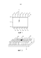
на Фиг. 1 показано схематическое изображение поперечного сечения детектора излучения со счетом фотонов.in FIG. 1 is a schematic cross-sectional view of a photon counting radiation detector.
На Фиг. 2 показано схематическое изображение антирассеивающей решетки поверх детектора излучения с одной областью, заблокированной от излучения.FIG. 2 is a schematic illustration of an anti-scatter grating over a radiation detector with one area blocked from radiation.
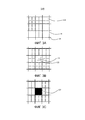
На Фиг. 3 показаны схематические изображения вида сверху матрицы пикселей детектора, в которой никакие пиксели не блокируются от излучения (Фиг. 3А, 3В), матрицы пикселей детектора с заблокированными пикселями, образующими зону компенсации в соответствии с настоящим изобретением (Фиг. 3C).FIG. 3 is a schematic top view of a detector pixel array in which no pixels are blocked from radiation (FIGS. 3A, 3B), a detector pixel array with blocked pixels forming a compensation zone in accordance with the present invention (FIG. 3C).
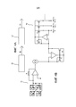
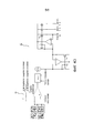
На фиг. 4 показана электрическая реализация измерения темнового тока и выдачи тока компенсации в соответствии с настоящим изобретением, где Фиг. 4А представляет собой схематическое изображение основных компонентов, а на Фиг. 4B, 4C и 4D показаны примеры того, как это может быть реализовано в электрическом контуре.FIG. 4 shows an electrical implementation of dark current measurement and supply of compensation current according to the present invention, where FIG. 4A is a schematic diagram of the main components, and FIG. 4B, 4C and 4D show examples of how this might be implemented in an electrical circuit.
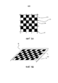
На Фиг. 5А изображена матрица пикселей, которые в виде регулярного рисунка блокируются от излучения. На Фиг. 5B показана структура маски, которая может использоваться для получения регулярного рисунка для блокировки пикселей детектора.FIG. 5A shows a matrix of pixels that are blocked from radiation in a regular pattern. FIG. 5B shows a mask structure that can be used to obtain a regular pattern to block detector pixels.
Изобретение может принимать форму в виде различных компонентов и расположений компонентов, а также в виде различных операций процесса и схем операций процесса. Чертежи приведены только с целью иллюстрации предпочтительных вариантов осуществления и не должны толковаться как ограничивающие данное изобретение. Чтобы лучше визуализировать некоторые признаки могут быть опущены или размеры могут не быть не в масштабе.The invention can take form in various components and component arrangements, as well as in various process steps and process flow diagrams. The drawings are for the purpose of illustrating preferred embodiments only and should not be construed as limiting the invention. For better visualization, some features may be omitted or dimensions may not be out of scale.
ПОДРОБНОЕ ОПИСАНИЕ ВАРИАНТОВ ОСУЩЕСТВЛЕНИЯDETAILED DESCRIPTION OF IMPLEMENTATION OPTIONS
Детекторы излучения используются для получения информации об изображении объекта (например, человека), который облучается посредством источника излучения. Все неослабленное излучение проходит объект для входа в детектор излучения, где излучение преобразуется в информацию об изображении. Можно использовать альтернативные детекторы излучения, например, в астрономии или фотографии, где входящее излучение обнаруживается для выдачи информации об объекте или его изображения.Radiation detectors are used to obtain information about the image of an object (for example, a person) that is irradiated by a radiation source. All unreduced radiation passes through the object to enter the radiation detector, where the radiation is converted into image information. Alternative radiation detectors can be used, for example in astronomy or photography, where incoming radiation is detected to provide information about the object or its image.
Настоящее изобретение относится к компенсации дрейфа темнового тока в детекторах для счета фотонов, таких как, например, используемых для визуализации спектрального излучения. Часто эти детекторы основаны на принципе прямого преобразования излучения. На Фиг. 1 показано очень схематичное изображение детектора прямого преобразования 10 для счета фотонов в поперечном сечении.The present invention relates to compensation for dark current drift in photon counting detectors, such as those used, for example, for imaging spectral radiation. These detectors are often based on the principle of direct conversion of radiation. FIG. 1 shows a very schematic cross-sectional view of a
Объем детектора 1 прямого преобразования фотонов для счета фотонов образуется слоем 11 материала прямого преобразования. Слой 11 материала прямого преобразования может состоять из монокристаллического полупроводникового материала, который является материалом с собственной электропроводностью или имеет полностью обедненную p-i-n структуру. CZT является подходящим полупроводниковым материалом в свете вариантов осуществления настоящего изобретения, но другие материалы прямого преобразования, известные специалисту в данной области, также выиграют от преимуществ настоящего изобретения (например, CdTe, Si, GaAs и т. д.). Слой 11 прямого преобразования помещается между катодом 12 детектора и анодом 13 детектора. Катод детектора удерживается с отрицательным потенциалом смещения, в то время как анод детектора удерживается с меньшим отталкивающим (обычно притягивающим положительным) потенциалом. Катод 12 детектора образует сплошной слой на слое 11 прямого преобразования и, как правило, прозрачен (или имеет незначительное поглощение) для фотонов с уровнем энергии, которые должны быть обнаружены детектором прямого преобразования для счета фотонов. Анод 13 детектора находится на противоположной стороне слоя 11 прямого преобразования и образован из матрицы 13 пикселей 131 детектора.The volume of the photon
Когда фотон х проходит катод 12 детектора и проникает в слой 11 материала прямого преобразования, фотон взаимодействует с материалом прямого преобразования, чтобы генерировать многочисленные электронно-дырочные пары. Положительно заряженные дырки дрейфуют к сильно отрицательно заряженному катоду 12 детектора, а отрицательно заряженные электроны дрейфуют к более положительно заряженному аноду 13 детектора. Когда электроны приближаются к аноду 13 детектора, каждый пиксель 131 детектора индуцирует сигнал (как правило, ток), который после сбора указывает на заряд электронного облака, которое приближается к этому конкретному пикселю 131 электрода. Затем генерируемый сигнал дополнительно обрабатывается блоками обработки (не показаны), подсчитывается генерируемая оценка энергии падающего фотона (ов) внутри множества так называемых энергетических интервалов. В конечном итоге информация отображается на блоке (не показан) дисплея пользователю в виде письменной информации или в виде восстановленного изображения (части) исследуемого объекта.When the x photon passes the
В некоторых случаях фотоны могут не подсчитываться исправным пикселем, например, в силу помех или фотонов, падающих в объеме над зазором двух соседних анодов или под углами, сильно отклоняющимися от нормали. Существуют различные способы решения этой проблемы. Одним особенно часто используемым решением является использование антирассеивающей решетки (ASG) 14, которая представляет собой структуру, размещенную на детекторе 10, со стенками, выполненными из поглощающего излучение материала, такого как вольфрам, выступающую практически перпендикулярно от поверхности детектора к источнику излучения. Фотоны, входящие под слишком большим углом, отклоняющимся от нормали, поглощаются или отводятся стенками 14. На Фиг. 2 показано трехмерное изображение ASG 14, помещенной на детекторе 10. Стенки 14 ASG разделяют верхнюю поверхность на отдельные участки, обычно охватывающий один пиксель 131 или группу пикселей 131 (например, 2 на 2 пикселя).In some cases, photons may not be counted by a good pixel, for example, due to noise or photons falling in the volume over the gap of two adjacent anodes or at angles that strongly deviate from the normal. There are various ways to solve this problem. One particularly commonly used solution is the use of an anti-scatter grating (ASG) 14, which is a structure placed on the
Как уже упоминалось ранее, даже когда пиксели 131 прямого преобразования не облучаются, они по-прежнему генерируют небольшой ток, так называемый темновой ток, который обычно вызывается изменениями температуры или зависит от них. Необходимо скорректировать результирующее смещение базовой линии. Настоящее изобретение основано на понимании того, что пиксель 132, не облучаемый во время процедуры обнаружения излучения, генерирует только сигнал темнового тока в тех же условиях, что и другие облученные пиксели 131 («пиксели детектора») в матрице пикселей 13 анода. Это может быть достигнуто путем создания зоны 132 компенсации, состоящей из одного или более пикселей, которые экранированы от излучения. Когда измеряется ток от области 132 компенсации, это приводит к характерному значению темнового тока. Это значение темнового тока может затем использоваться для компенсации измеренного значения тока пикселов 131 обнаружения, например, путем простого вычитания текущего значения, измеренного из области 132 компенсации (скорректированного на количество пикселей в области 132 компенсации) из измеренного текущего значения каждого из пикселей 131 обнаружения.As mentioned earlier, even when the
Пиксель может быть экранирован от излучения путем использования поглощающего излучения, которое препятствует излучению достичь лежащего ниже пикселя. Это может быть реализовано путем использования полностью поглощающего материала в виде, например, поглощающего покрытия или поглощающей структуры, такой как блок или пластина, которые наносятся или помещаются на или выше пикселя, который должен быть экранирован. Экранирование также может быть реализовано с использованием комбинации покрытия и структуры. Преимущество использования покрытия состоит в том, что его относительно легко наносить на пиксель во время изготовления, например, путем печати. Однако полностью поглощающие покрытия могут быть труднодоступными для получения, особенно в случае тонких покрытий и/или излучения большой энергии. Структуры могут быть внедрены на стадии производства различными способами, например, их объединение с ASG или местом, литье или печать их на пикселе или над ним. Более толстые структуры более эффективны для блокирования излучения, но точное размещение имеет решающее значение. Экранирование также может быть выполнено вне детектора 10 излучения, например, посредством фильтра, расположенного между катодом 12 детектора и ASG 14 или, альтернативно, между источником излучения и детектором 10 излучения, хотя точное выставление может быть довольно сложным в этой ситуации.A pixel can be shielded from radiation by using absorbing radiation that prevents radiation from reaching the underlying pixel. This can be accomplished by using a fully absorbent material in the form of, for example, an absorbent coating or an absorbent structure such as a block or plate, which is applied or placed on or above the pixel to be shielded. Shielding can also be implemented using a combination of coating and structure. An advantage of using a coating is that it is relatively easy to apply to a pixel during manufacture, for example by printing. However, fully absorbing coatings can be difficult to obtain, especially in the case of thin coatings and / or high energy radiation. The structures can be implemented in the production stage in a variety of ways, such as combining them with an ASG or site, casting or printing them on or over a pixel. Thicker structures are more effective at blocking radiation, but precise placement is critical. Shielding can also be performed outside the
Альтернативно, для ASG структур, полученных лазерным спеканием, блокирующий элемент может быть сформирован на том же самом этапе процесса, что и сама ASG, что устраняет любое смещение или механическое перемещение. Однако это может привести к увеличению стоимости, обусловленному временем изготовления и материалом.Alternatively, for laser sintered ASG structures, the blocking element can be formed in the same process step as the ASG itself, eliminating any displacement or mechanical movement. However, this can lead to an increase in cost due to manufacturing time and material.
Примерный вариант осуществления, показанный на Фиг. 2, имеет матрицу 13 ASG с центральной областью, образующей область 132 компенсации, для которой полностью блокируются падающие рентгеновские лучи. Область 132 компенсации обеспечивается путем добавления высокопоглощающего материала и охватывает все пиксели детектора ниже. Обычно один или четыре пикселя в зависимости от субпикселирования детектора. На фигуре центральная область экранирована. Местоположение экранированной области может находиться в любом другом месте матрицы, но предпочтительно не на краю матрицы, так как изменения темнового тока могут не указывать на изменения тока в объеме CZT. Кроме того, матрица 13 и ASG 14 могут быть оснащены 1 или более из упомянутых областей 132 компенсации.The exemplary embodiment shown in FIG. 2 has an
На Фиг. 3А показано концептуальное представление известных анодов CZT, выставленных по отношению к ASG 14. В этом примере каждая секция ASG ограничивает 2×2 пикселей детектора. Пиксели в центральной секции ASG полностью поглощают рентгеновское излучение. На Фиг. 3В показан альтернативный вариант осуществления с другой геометрией анода с одиночным пикселем 131 в одной секции ASG, окруженным защитным кольцом 133, чтобы обеспечить надлежащее распределение электрического поля. Преимущество структуры, показанной на Фиг. 3B, состоит в том, что анод удерживается намеренно вдали от всех соседей, поэтому полностью устраняются ложные события, вызванные разделением заряда и/или k-уходом.FIG. 3A shows a conceptual representation of prior art CZT anodes exposed to
На Фиг. 3С область 132 компенсации образована путем экранирования 2×2 пикселей 131 в центральной секции ASG, показанной на Фиг. 3A, или одиночного пикселя 131 с защитным кольцом 133, показанным на Фиг. 3B, с материалом для защиты от излучения. Пиксель(-и) внизу не принимают никаких падающих фотонов, и единственным сигналом, присутствующим в соответствующих анодах, является их темновой ток. Упомянутый темновой ток измеряется и используется для выдачи тока компенсации для всех других пикселей 131 внутри матрицы 13. Это может быть сделано в предположении, что темновой ток, измеренный в заблокированной секции ASG, является показателем для темнового тока в разных местах объема. Степень, в которой это предположение будет выполняться, увеличивается с однородностью датчика и оправдывается тем фактом, что температурные дрейфы, вероятно, будут однородными на одном кристалле CZT, формирующемся на плитке детектора, соединенном с одним ASIC. Преимущество использования 2×2 экранированных пикселей 131 (как на Фиг. 3A) заключается в том, что получены четыре разных темновых измерения, которые могут быть усреднены, или выбросы могут быть проигнорированы, чтобы иметь меньшую зависимость от качества одного пикселя или (незначительной) разницы в размерах между пикселями. Преимущество использования одиночного пикселя 131 с защитным кольцом 134 (как на Фиг.3В) заключается в том, что получается центральное измерение внутри секции ASG и минимизируются побочные эффекты, такие как разделение заряда, от окружающих пикселей.FIG. 3C, the
На очень схематичном изображении Фиг. 4А показан определитель 41 темнового тока, который определяет значение I1 темнового тока от экранированного пикселя (пикселей) области 132 компенсации. Это значение темнового тока I1 затем используется как ввод для компенсатора 42 темнового тока, который обеспечивает компенсацию I2 темнового тока, которая используется для коррекции измеренного значения тока пикселей 131 обнаружения. Наиболее простой способ состоит в том, чтобы определить компенсацию темнового тока I2 как величину, противоположную определенному значению темнового тока I1 (I2=-I1). Другие способы компенсации, в которых для компенсации используется больший или меньший ток, также предусмотрены в настоящем изобретении.In a very schematic view of FIG. 4A shows a dark
Определение темнового тока из области 132 компенсации и компенсация темнового тока в пикселах 131 обнаружения могут осуществляться различными способами. Один иллюстративный вариант осуществления электрической схемы под областью 132 компенсации, содержащей четыре экранированных пикселя, показана на Фиг. 4В. Определитель 41 темнового тока содержит простой управляемый током усилитель напряжения, который используется, например, для генерации напряжения, пропорционального темновому току, присутствующему в четырех одиночных пикселях. Затем генерируется ток, соответствующий тому же темновому току (или любой величине, представляющей темновой ток). В компенсаторе 42 темнового тока этот ток инвертируется по знаку (положительный на отрицательный или наоборот) с использованием двух регулируемых токовых зеркал. Один выходной ток компенсации на пиксель затем распределяется по всей матрице. Токовые зеркала, показанные на Фиг. 4B, известны из US 20110168892 A1, но также возможны и рассматриваются другие известные топологии зеркал. Выходной ток этой схемы, который равен темновому току и имеет надлежащий знак, должен быть подан во все пиксели 131 обнаружения (пиксель N, пиксель N+1, пиксель N+2 и т. д.), незащищенные от излучения в матрице. Эффективно, чтобы все пиксели 131 обнаружения в матрице компенсировались. Знаки тока и необходимость одного или двух токовых зеркал будут зависеть от реализации управляемого током усилителя напряжения и управляемого напряжением источника. В примере, показанном на Фиг. 4В, где для определения темнового тока используются четыре пикселя, выходной ток на пиксель предпочтительно составляет четверть полученного темнового тока. Этот коэффициент усиления может быть реализован на управляемом напряжением токе или путем простого доведения до нужных размеров транзисторов, образующих токовые зеркала.Determination of the dark current from the
Компенсация идеальна для случая, когда вся матрица 13 имеет одну и ту же температуру. Даже если точный темновой ток может различаться по всей матрице 13, компенсация гарантирует, что дрейф, вызванный температурой, не повлияет на оценку энергии, т. е. некоторое количество темнового тока может все еще присутствовать, но со временем не будет колебаться. Только тогда, когда температура в матрице 13 имеет значительный градиент по всей матрице (например, 2 градуса Цельсия), размер компенсации может быть недостаточным, но, тем не менее, она будет минимизировать дрейфы базовой линии.The compensation is ideal when the
В качестве расширения варианта осуществления, показанного на Фиг. 4В, несколько областей 132 компенсации охватывают, например, четыре отдельных экранированных пикселя или четыре группы из 2×2 экранированных пикселей, каждый из которых вблизи, но не в четырех углах кристалла CZT. Таким образом, может быть получена лучшая выборка темнового тока, а также градиентов темнового тока на датчике в обоих направлениях. Однако для реализации интерполяции (или экстраполяции к периферийным областям датчика) темновых токов, которые нужно вычесть, требуется более сложная электроника.As an extension of the embodiment shown in FIG. 4B, the plurality of
На Фиг. 4С схематически показан вариант осуществления, который позволяет распределять ток компенсации по пикселям. Этот конкретный вариант осуществления требует маршрутизации стольких из сигналов, сколько пикселей 131, которые присутствуют в матрице 13. Более практичная реализация заключается в перемещении выхода ветви токового зеркала на каждый пиксель. Таким образом, должно быть распределено только напряжение управления, которое является общим для всех пикселей 131, то есть область 132 компенсации (центральная секция изображенной схемы) имеет только одиночный выход, который затем направляется на пиксели 131 обнаружения. В еще одной альтернативе токовое зеркало может оставаться внутри центрального пикселя, но распространяется только на один пиксель. Затем может использоваться схема регенерации тока на каждом пикселе для перераспределения на соседа и так далее и так далее. Такая схема регенерации, например, известна из US 20110168892 A1.FIG. 4C is a schematic diagram of an embodiment that allows the compensation current to be distributed across pixels. This particular embodiment requires routing as many of the signals as there are
Схема, показанная на Фиг. 4B, работает непрерывно. Поэтому конструкция управляемого током усилителя напряжения является критичной с точки зрения шума, и коррекция будет сильно зависеть от усилителя, имеющего очень небольшое входное смещение. Следовательно, более адекватная реализация может состоять из этапа интегратора, за которым следует этап взятия замера и удержания. Таким образом, компенсация может обновляться с заданными временными интервалами (например, одна на кадр). Поскольку изменения темнового тока в основном проявляются как низкочастотные компоненты, может быть достаточным обновление с временными интервалами один раз на один или более кадров. Примерный вариант осуществления для реализации этого показан на Фиг. 4D. Интегратор значительно улучшает шумовые характеристики и позволяет реализовать метод двойной коррелированной выборки (ДКВ) для устранения влияния шума ненулевого смещения входного сигнала и розового шума, например, как известно из R. Steadman и др. «A CMOS Photodiode Array with In-Pixel Data Acquisition System for Computed tomography», IEEE JSSC 2004, том 39).The circuit shown in FIG. 4B, works continuously. Therefore, the design of a current controlled voltage amplifier is critical in terms of noise, and correction will be highly dependent on the amplifier having very little input offset. Therefore, a more adequate implementation might consist of an integrator stage followed by a sampling and holding stage. Thus, the compensation can be updated at predetermined time intervals (eg, one per frame). Since changes in dark current mainly appear as low frequency components, a time slot update once per one or more frames may be sufficient. An exemplary embodiment for doing this is shown in FIG. 4D. The integrator significantly improves the noise performance and allows the implementation of a double correlated sampling (DQS) method to eliminate the influence of non-zero offset noise of the input signal and pink noise, for example, as is known from R. Steadman et al. “A CMOS Photodiode Array with In-Pixel Data Acquisition System for Computed tomography, IEEE JSSC 2004, Volume 39).
В еще одном варианте осуществления настоящего изобретения предлагается воздерживаться от компенсации темнового тока с помощью аппаратного обеспечения. В качестве альтернативы, показания темнового тока периодически замеряются во время работы детектора, но с частотой выборки, как правило, намного ниже частоты выборки самого детектора ввиду очень медленных изменений температуры, ожидаемых во время сканирования. Выбранные значения оцифровываются и отправляются вместе с данными визуализации для реконструкции. Во время реконструкции изображения изменения темнового тока во времени переводятся в изменения сдвигов энергетических порогов, основанных на усилении зарядочувствительного усилителя. Пока сдвиги, вызванные изменениями температуры, остаются ниже нескольких кВ для зарегистрированной энергии, отсутствие их компенсации в аппаратных средствах, не будет нести значительную потерю спектральных характеристик.In yet another embodiment of the present invention, it is proposed to refrain from compensating for dark current with hardware. Alternatively, dark current readings are sampled periodically while the detector is operating, but with a sampling rate that is typically much lower than that of the detector itself due to the very slow temperature changes expected during scanning. The selected values are digitized and sent along with the visualization data for reconstruction. During image reconstruction, changes in dark current over time are translated into changes in energy threshold shifts based on the gain of the charge-sensitive amplifier. As long as shifts due to temperature changes remain below a few kV for recorded energy, lack of compensation in hardware will not result in significant loss of spectral performance.
На Фиг. 5А показан еще один вариант осуществления, в котором каждый второй пиксель 131 в матрице 13 экранирован от формирующего излучение рисунка областей 132 компенсации. В этом примере показан обычный рисунок шахматной доски, покрывающий каждый второй пиксель в шахматном порядке. Помимо ранее описанных преимуществ, этот вариант осуществления предлагает еще больше преимуществ, помимо тех, которые были упомянуты ранее, в частности для визуализации с подсчетом фотонов сверхвысокой энергии (UHR).FIG. 5A shows another embodiment in which every
ASG 14 уже способствует минимизации разделения заряда, несмотря на то, что они обычно расположены с большим шагом, чем пиксели самого детектора. ASG с более мелким шагом улучшают энергетический отклик за счет более высокой сложности и стоимости изготовления. Для большого количества применений это может и не понадобиться. При экранировании каждого второго пикселя от излучения низкоэнергетический остаток избирательно уменьшается, тем самым значительно улучшая энергетическое разрешение для ограниченного числа конкретных протоколов.
Этот вариант осуществления можно рассматривать как получение режима со сверхвысоким энергетическим разрешением (UHER), который особенно подходит для конкретного приложения для получения изображений с использованием счета фотонов, которые выигрывают от более высокого энергетического разрешения. Аналогично сверхвысокому разрешению UHR снижается эффективная облученная область детектора. Однако в этом случае достигается не только лучшее пространственное разрешение, но также обеспечивается то, что экспонированные пиксели дают наилучший энергетический отклик, в значительной степени не влияющий на разделение заряда от соседних пикселей. В варианте осуществления, показанном на Фиг. 5В, в отличие от обычного UHR, экранирующая маска 15 не состоит из одиночных прорезей (вдоль оси вращения), а скорее, выполнена как рисунок шахматной доски с отверстиями 151 и экранирующими секциями 152 на половине шага ASG.This embodiment can be seen as obtaining a Ultra High Energy Resolution (UHER) mode that is particularly suited for a particular photon counting imaging application that benefits from a higher energy resolution. Similar to ultra-high resolution UHR, the effective irradiated area of the detector is reduced. However, this not only achieves better spatial resolution, but also ensures that the exposed pixels give the best energy response without significantly affecting charge separation from neighboring pixels. In the embodiment shown in FIG. 5B, unlike a conventional UHR, the shielding
Экранирующие секции 152 предпочтительно выполнены из материала, поглощающего рентгеновское излучение, например, вольфрама, тантала, молибдена или подобного материала достаточной толщины (например, 100-200 мкм). Экранирующие области 152 и отверстия 151 имеют тот же размер, что и пиксели детектора, и их необходимо полностью выставить для оптимального использования преимуществ.The shielding
Для шага ASG, например, приблизительно 1 квадратный миллиметр, предполагается, что детектор будет демонстрировать субпикселирование 1:4, то есть каждая секция ASG, образованная областью, заключенной в стенках ASG 14, выставлена и ограничивает детектор в 2×2 пикселя. Таким образом, вышеупомянутый шахматный рисунок гарантирует, что для каждой секции ASG облучаются только два пикселя детектора (по диагонали). Это значительно снижает вероятность разделения заряда. Только ASG уже низкоэнергетический конец наполовину (вызванный разделением заряда). Дополнительная UHER решетка 15 еще уменьшит оставшийся конец на 90%, что даст почти идеальный спектральный отклик.For an ASG pitch of, for example, approximately 1 square millimeter, it is assumed that the detector will exhibit 1: 4 subpixelation, that is, each ASG section formed by the area enclosed in the walls of the
Преимущества настоящего изобретения не ограничиваются геометрией и количеством пикселей, изображенных в вариантах осуществления. Другие геометрии, пропорции, количество экранированных пикселей (например, 1×2, 3×3, …) и/или реализация схемы могут быть реализованы для всех вариантов осуществления. Схемы, показанные на Фиг. 4А, В и С, требуют адаптации, которую квалифицированный специалист должен знать, как реализовать, чтобы соответствовать варианту одного пикселя, показанному на Фиг. 3В или Фиг. 5А.The advantages of the present invention are not limited to the geometry and number of pixels depicted in the embodiments. Other geometries, aspect ratios, number of escaped pixels (eg, 1 × 2, 3 × 3, ...) and / or circuit implementation may be implemented for all embodiments. The circuits shown in FIG. 4A, B, and C require adaptation that a skilled person should know how to implement to match the single pixel embodiment shown in FIG. 3B or FIG. 5A.
Настоящее изобретение относится к детекторам излучения, в частности к детекторам рентгеновского излучения, которые используются для обеспечения безопасности или медицинской визуализации, такие как, например, формирователи изображений компьютерной томографии.The present invention relates to radiation detectors, in particular to X-ray detectors that are used for safety or medical imaging, such as, for example, computed tomography imaging devices.
Хотя изобретение было проиллюстрировано и подробно описано на чертежах и предшествующем описании, такие иллюстрации и описание должны рассматриваться как иллюстративные или приведенные в качестве примера, а не ограничивающие; изобретение не ограничивается описанными вариантами осуществления.Although the invention has been illustrated and described in detail in the drawings and the foregoing description, such illustrations and description are to be regarded as illustrative or exemplary and not restrictive; the invention is not limited to the described embodiments.
Изучив чертежи, раскрытие и приложенную формулу изобретения, специалисты в данной области смогут понять и осуществить при практической реализации заявленного изобретения другие вариации показанных вариантов осуществления. В формуле изобретения слово «содержит» не исключает других элементов или этапов, а упоминание элемента в единственном числе не исключают множества таких элементов. Один процессор или другой блок может выполнить функции нескольких пунктов, перечисленных в формуле изобретения. Сам факт того, что определенные меры перечислены во взаимно отличных зависимых пунктах формулы изобретения, не указывает на то, что сочетание этих мер нельзя использовать с пользой.Having studied the drawings, the disclosure, and the appended claims, those skilled in the art will be able to understand and practice other variations of the illustrated embodiments in the practice of the claimed invention. In the claims, the word “comprises” does not exclude other elements or steps, and references to an element in the singular do not exclude many such elements. One processor or other unit may fulfill the functions of more than one item recited in the claims. The mere fact that certain measures are listed in mutually different dependent claims does not indicate that the combination of these measures cannot be used to advantage.
Любые ссылочные позиции в формуле изобретения не должны рассматриваться в качестве ограничения объема.Any reference numbers in the claims should not be construed as limiting the scope.
Claims (19)
Applications Claiming Priority (3)
| Application Number | Priority Date | Filing Date | Title |
|---|---|---|---|
| EP15196524.1 | 2015-11-26 | ||
| EP15196524 | 2015-11-26 | ||
| PCT/EP2016/078481 WO2017089363A1 (en) | 2015-11-26 | 2016-11-23 | Dark current compensation |
Publications (3)
| Publication Number | Publication Date |
|---|---|
| RU2018122963A RU2018122963A (en) | 2019-12-26 |
| RU2018122963A3 RU2018122963A3 (en) | 2020-02-10 |
| RU2734452C2 true RU2734452C2 (en) | 2020-10-16 |
Family
ID=54705437
Family Applications (1)
| Application Number | Title | Priority Date | Filing Date |
|---|---|---|---|
| RU2018122963A RU2734452C2 (en) | 2015-11-26 | 2016-11-23 | Dark current compensation |
Country Status (6)
| Country | Link |
|---|---|
| US (1) | US10267928B2 (en) |
| EP (1) | EP3380870A1 (en) |
| JP (1) | JP6924755B2 (en) |
| CN (1) | CN108291973B (en) |
| RU (1) | RU2734452C2 (en) |
| WO (1) | WO2017089363A1 (en) |
Families Citing this family (7)
| Publication number | Priority date | Publication date | Assignee | Title |
|---|---|---|---|---|
| CN110914713B (en) | 2017-07-26 | 2023-07-18 | 深圳帧观德芯科技有限公司 | X-ray detector capable of managing peripheral charge sharing |
| EP3444826A1 (en) * | 2017-08-14 | 2019-02-20 | Koninklijke Philips N.V. | Low profile anti scatter and anti charge sharing grid for photon counting computed tomography |
| WO2019084704A1 (en) * | 2017-10-30 | 2019-05-09 | Shenzhen Xpectvision Technology Co., Ltd. | Dark noise compensation in radiation detector |
| EP3567405A1 (en) | 2018-05-08 | 2019-11-13 | Koninklijke Philips N.V. | Photon counting spectral ct |
| US10813607B2 (en) * | 2018-06-27 | 2020-10-27 | Prismatic Sensors Ab | X-ray sensor, method for constructing an x-ray sensor and an x-ray imaging system comprising such an x-ray sensor |
| US20220303481A1 (en) * | 2021-03-18 | 2022-09-22 | Taiwan Semiconductor Manufacturing Company Limited | Pixel array including dark pixel sensors |
| JP7439027B2 (en) | 2021-09-08 | 2024-02-27 | 富士フイルムヘルスケア株式会社 | Radiation imaging device and radiation detector |
Citations (5)
| Publication number | Priority date | Publication date | Assignee | Title |
|---|---|---|---|---|
| US20080099689A1 (en) * | 2006-10-31 | 2008-05-01 | Einar Nygard | Photon counting imaging detector system |
| WO2010007544A1 (en) * | 2008-07-14 | 2010-01-21 | Koninklijke Philips Electronics N.V. | Anti-scatter grid |
| RU2411542C2 (en) * | 2005-04-22 | 2011-02-10 | Конинклейке Филипс Электроникс Н.В. | Digital silicon photomultiplier for tof-pet |
| US20110248175A1 (en) * | 2008-12-15 | 2011-10-13 | Koninklijke Philips Electronics N.V. | Temperature compensation circuit for silicon photomultipliers and other single photon counters |
| US20140014818A1 (en) * | 2012-07-13 | 2014-01-16 | Young Sung CHO | Pixel array, image sensor including the same, and method of compensating for local dark current |
Family Cites Families (19)
| Publication number | Priority date | Publication date | Assignee | Title |
|---|---|---|---|---|
| JP4100739B2 (en) | 1996-10-24 | 2008-06-11 | キヤノン株式会社 | Photoelectric conversion device |
| DE19734717A1 (en) * | 1997-08-11 | 1999-02-25 | Sirona Dental Systems Gmbh | Method for compensating the dark current when creating dental panoramic and / or cephalometric slice images |
| JP3832615B2 (en) * | 1999-08-26 | 2006-10-11 | 株式会社島津製作所 | Radiation detector |
| GB2370960A (en) | 2001-01-05 | 2002-07-10 | Spectral Fusion Technologies L | Partially shielded photodiode array |
| JP2001340324A (en) * | 2001-03-16 | 2001-12-11 | Toshiba Medical System Co Ltd | X-ray detector and radiodiagnostic device using the same |
| JP4723767B2 (en) * | 2001-09-13 | 2011-07-13 | 株式会社東芝 | X-ray diagnostic imaging equipment |
| JP2003209665A (en) | 2002-01-16 | 2003-07-25 | Fuji Photo Film Co Ltd | Image reading method and image recording reader |
| WO2004019411A1 (en) * | 2002-08-09 | 2004-03-04 | Hamamatsu Photonics K.K. | Photodiode array, production method therefor, and radiation detector |
| US20110168892A1 (en) | 2005-01-06 | 2011-07-14 | Koninklijke Philips Electronics N.V. | Pixel Implemented Current Amplifier |
| JP4555785B2 (en) | 2006-02-10 | 2010-10-06 | シャープ株式会社 | Fixed pattern noise removal device, solid-state imaging device, electronic device, and fixed pattern noise removal program |
| JP5458260B2 (en) | 2006-09-25 | 2014-04-02 | コーニンクレッカ フィリップス エヌ ヴェ | Leakage current and residual signal compensation for integral detectors based on direct X-ray conversion |
| JP4462299B2 (en) * | 2007-07-17 | 2010-05-12 | ソニー株式会社 | Imaging apparatus, image processing method, and computer program |
| JP2009284424A (en) | 2008-05-26 | 2009-12-03 | Sony Corp | Imaging apparatus, imaging method, and program |
| JP2012508375A (en) * | 2008-11-10 | 2012-04-05 | コーニンクレッカ フィリップス エレクトロニクス エヌ ヴィ | Converter elements for radiation detectors |
| RU2518589C2 (en) * | 2009-03-06 | 2014-06-10 | Конинклейке Филипс Электроникс Н.В. | Advanced temperature compensation and control circuit for single-photon counter |
| JP2012045044A (en) * | 2010-08-24 | 2012-03-08 | Fujifilm Corp | Radiation image detection device |
| RU2581720C2 (en) | 2011-01-10 | 2016-04-20 | Конинклейке Филипс Электроникс Н.В. | Detection device for detection of photons emitted by radiation source |
| US9510792B2 (en) * | 2013-05-17 | 2016-12-06 | Toshiba Medical Systems Corporation | Apparatus and method for collimating X-rays in spectral computer tomography imaging |
| JP2015021843A (en) * | 2013-07-19 | 2015-02-02 | 株式会社島津製作所 | Radiation detector, radiation detection device and radiation analysis device |
-
2016
- 2016-11-23 RU RU2018122963A patent/RU2734452C2/en active
- 2016-11-23 US US15/776,096 patent/US10267928B2/en active Active
- 2016-11-23 WO PCT/EP2016/078481 patent/WO2017089363A1/en active Application Filing
- 2016-11-23 CN CN201680069127.6A patent/CN108291973B/en active Active
- 2016-11-23 JP JP2018526916A patent/JP6924755B2/en active Active
- 2016-11-23 EP EP16801180.7A patent/EP3380870A1/en not_active Withdrawn
Patent Citations (5)
| Publication number | Priority date | Publication date | Assignee | Title |
|---|---|---|---|---|
| RU2411542C2 (en) * | 2005-04-22 | 2011-02-10 | Конинклейке Филипс Электроникс Н.В. | Digital silicon photomultiplier for tof-pet |
| US20080099689A1 (en) * | 2006-10-31 | 2008-05-01 | Einar Nygard | Photon counting imaging detector system |
| WO2010007544A1 (en) * | 2008-07-14 | 2010-01-21 | Koninklijke Philips Electronics N.V. | Anti-scatter grid |
| US20110248175A1 (en) * | 2008-12-15 | 2011-10-13 | Koninklijke Philips Electronics N.V. | Temperature compensation circuit for silicon photomultipliers and other single photon counters |
| US20140014818A1 (en) * | 2012-07-13 | 2014-01-16 | Young Sung CHO | Pixel array, image sensor including the same, and method of compensating for local dark current |
Also Published As
| Publication number | Publication date |
|---|---|
| US20180321395A1 (en) | 2018-11-08 |
| CN108291973B (en) | 2022-09-09 |
| RU2018122963A (en) | 2019-12-26 |
| WO2017089363A1 (en) | 2017-06-01 |
| JP2019504297A (en) | 2019-02-14 |
| EP3380870A1 (en) | 2018-10-03 |
| US10267928B2 (en) | 2019-04-23 |
| CN108291973A (en) | 2018-07-17 |
| JP6924755B2 (en) | 2021-08-25 |
| RU2018122963A3 (en) | 2020-02-10 |
Similar Documents
| Publication | Publication Date | Title |
|---|---|---|
| RU2734452C2 (en) | Dark current compensation | |
| JP4989005B2 (en) | Digital X-ray imaging method and sensor device | |
| EP1828810B1 (en) | Pulsed x-ray for continuous detector correction | |
| Ballabriga et al. | Characterization of the Medipix3 pixel readout chip | |
| Overdick et al. | Status of direct conversion detectors for medical imaging with X-rays | |
| EP3791213B1 (en) | Photon counting spectral ct | |
| CN106255901B (en) | Method of calibrating a photon detector, absorption filter assembly and imaging apparatus | |
| US8084746B2 (en) | Radiation detector and detection method having reduced polarization | |
| Becker et al. | Characterization of chromium compensated GaAs as an X-ray sensor material for charge-integrating pixel array detectors | |
| US9620256B2 (en) | X-ray imaging device including anti-scatter grid | |
| Becker et al. | Characterization of CdTe sensors with Schottky contacts coupled to charge-integrating pixel array detectors for X-ray science | |
| Street et al. | High-resolution direct-detection x-ray imagers | |
| Schwarz et al. | X-ray imaging using a hybrid photon counting GaAs pixel detector | |
| Hunt et al. | Imaging performance of an amorphous selenium flat-panel detector for digital fluoroscopy | |
| Green et al. | Calibration and post-processing for photon-integrating pixel array detectors | |
| Zang et al. | The Dosepix detector—an energy-resolving photon-counting pixel detector for spectrometric measurements | |
| CN108324298B (en) | X-ray detector with an arrangement of a pixelated second electrode and a scattered radiation grid | |
| Street et al. | High-resolution x-ray image sensors based on HgI2 | |
| Delpierre et al. | Large surface X-ray pixel detector | |
| EP3536243A1 (en) | Improved image acquisition | |
| Cartier et al. | Study of the signal response of the MÖNCH 25μm pitch hybrid pixel detector at different photon absorption depths | |
| Nachtrab et al. | Simple solutions for spectroscopic, photon counting X-ray imaging detectors | |
| Zhu et al. | Stability and characteristics of 3D HgI2 detectors at different cathode bias | |
| Ahluwalia | Imaging and Detection | |
| Schwarz et al. | Dose-dependent X-ray measurements using a 64× 64 hybrid GaAs pixel detector with photon counting |