RU2670303C2 - Functional thin film and method of its manufacture - Google Patents
Functional thin film and method of its manufacture Download PDFInfo
- Publication number
- RU2670303C2 RU2670303C2 RU2016111693A RU2016111693A RU2670303C2 RU 2670303 C2 RU2670303 C2 RU 2670303C2 RU 2016111693 A RU2016111693 A RU 2016111693A RU 2016111693 A RU2016111693 A RU 2016111693A RU 2670303 C2 RU2670303 C2 RU 2670303C2
- Authority
- RU
- Russia
- Prior art keywords
- thin film
- group
- organic
- inorganic
- functional thin
- Prior art date
Links
- 239000010409 thin film Substances 0.000 title claims abstract description 191
- 238000004519 manufacturing process Methods 0.000 title claims abstract description 45
- 238000000034 method Methods 0.000 title claims abstract description 39
- 239000002243 precursor Substances 0.000 claims abstract description 71
- 229910044991 metal oxide Inorganic materials 0.000 claims abstract description 7
- 150000004706 metal oxides Chemical class 0.000 claims abstract description 7
- 150000001875 compounds Chemical class 0.000 claims description 44
- 239000000758 substrate Substances 0.000 claims description 20
- 230000015572 biosynthetic process Effects 0.000 claims description 17
- 125000003396 thiol group Chemical group [H]S* 0.000 claims description 12
- 239000002052 molecular layer Substances 0.000 claims description 11
- 229910052710 silicon Inorganic materials 0.000 claims description 11
- 125000000217 alkyl group Chemical group 0.000 claims description 9
- 229910052782 aluminium Inorganic materials 0.000 claims description 9
- 229910052793 cadmium Inorganic materials 0.000 claims description 9
- 229910052802 copper Inorganic materials 0.000 claims description 9
- 229910052733 gallium Inorganic materials 0.000 claims description 9
- 125000002887 hydroxy group Chemical group [H]O* 0.000 claims description 9
- 229910052738 indium Inorganic materials 0.000 claims description 9
- 229910052742 iron Inorganic materials 0.000 claims description 9
- 229910052748 manganese Inorganic materials 0.000 claims description 9
- 229910052758 niobium Inorganic materials 0.000 claims description 9
- 229910052718 tin Inorganic materials 0.000 claims description 9
- 229910052719 titanium Inorganic materials 0.000 claims description 9
- 229910052721 tungsten Inorganic materials 0.000 claims description 9
- 229910052720 vanadium Inorganic materials 0.000 claims description 9
- 229910052725 zinc Inorganic materials 0.000 claims description 9
- 229910052726 zirconium Inorganic materials 0.000 claims description 9
- 229910052751 metal Inorganic materials 0.000 claims description 7
- 239000002184 metal Substances 0.000 claims description 7
- 125000003118 aryl group Chemical group 0.000 claims description 6
- 125000004429 atom Chemical group 0.000 claims description 6
- 125000000753 cycloalkyl group Chemical group 0.000 claims description 6
- 125000001072 heteroaryl group Chemical group 0.000 claims description 6
- 229910052760 oxygen Inorganic materials 0.000 claims description 6
- 125000003178 carboxy group Chemical group [H]OC(*)=O 0.000 claims description 5
- 239000011248 coating agent Substances 0.000 claims description 5
- 238000000576 coating method Methods 0.000 claims description 5
- 101100134925 Gallus gallus COR6 gene Chemical group 0.000 claims description 4
- MUBZPKHOEPUJKR-UHFFFAOYSA-N Oxalic acid Chemical group OC(=O)C(O)=O MUBZPKHOEPUJKR-UHFFFAOYSA-N 0.000 claims description 4
- 150000004703 alkoxides Chemical class 0.000 claims description 4
- 125000003545 alkoxy group Chemical group 0.000 claims description 4
- 125000003277 amino group Chemical group 0.000 claims description 4
- 125000001033 ether group Chemical group 0.000 claims description 4
- 239000001257 hydrogen Substances 0.000 claims description 4
- 229910052739 hydrogen Inorganic materials 0.000 claims description 4
- 125000004435 hydrogen atom Chemical group [H]* 0.000 claims description 4
- NHNBFGGVMKEFGY-UHFFFAOYSA-N nitrate group Chemical group [N+](=O)([O-])[O-] NHNBFGGVMKEFGY-UHFFFAOYSA-N 0.000 claims description 4
- 230000003647 oxidation Effects 0.000 claims description 4
- 238000007254 oxidation reaction Methods 0.000 claims description 4
- QTBSBXVTEAMEQO-UHFFFAOYSA-N Acetic acid Chemical group CC(O)=O QTBSBXVTEAMEQO-UHFFFAOYSA-N 0.000 claims description 3
- VEXZGXHMUGYJMC-UHFFFAOYSA-N Hydrochloric acid Chemical group Cl VEXZGXHMUGYJMC-UHFFFAOYSA-N 0.000 claims description 3
- 125000005587 carbonate group Chemical group 0.000 claims description 3
- 229910002091 carbon monoxide Inorganic materials 0.000 claims description 2
- 238000006243 chemical reaction Methods 0.000 claims description 2
- 239000011521 glass Substances 0.000 claims description 2
- 238000011534 incubation Methods 0.000 claims description 2
- 229910052757 nitrogen Inorganic materials 0.000 claims description 2
- 239000004033 plastic Substances 0.000 claims description 2
- 239000010703 silicon Substances 0.000 claims description 2
- 229910052717 sulfur Inorganic materials 0.000 claims description 2
- 238000005516 engineering process Methods 0.000 abstract description 7
- 125000000524 functional group Chemical group 0.000 abstract description 7
- 239000000126 substance Substances 0.000 abstract description 5
- 238000011161 development Methods 0.000 abstract description 3
- 238000012986 modification Methods 0.000 abstract description 3
- 230000004048 modification Effects 0.000 abstract description 3
- 239000004065 semiconductor Substances 0.000 abstract description 3
- 230000000694 effects Effects 0.000 abstract description 2
- JLTRXTDYQLMHGR-UHFFFAOYSA-N trimethylaluminium Chemical compound C[Al](C)C JLTRXTDYQLMHGR-UHFFFAOYSA-N 0.000 description 27
- HQWPLXHWEZZGKY-UHFFFAOYSA-N diethylzinc Chemical compound CC[Zn]CC HQWPLXHWEZZGKY-UHFFFAOYSA-N 0.000 description 25
- 239000010410 layer Substances 0.000 description 19
- BXAVKNRWVKUTLY-UHFFFAOYSA-N 4-sulfanylphenol Chemical compound OC1=CC=C(S)C=C1 BXAVKNRWVKUTLY-UHFFFAOYSA-N 0.000 description 17
- 239000010408 film Substances 0.000 description 16
- 230000000052 comparative effect Effects 0.000 description 14
- 238000002474 experimental method Methods 0.000 description 14
- 229910018072 Al 2 O 3 Inorganic materials 0.000 description 10
- QIGBRXMKCJKVMJ-UHFFFAOYSA-N Hydroquinone Chemical compound OC1=CC=C(O)C=C1 QIGBRXMKCJKVMJ-UHFFFAOYSA-N 0.000 description 8
- 238000000151 deposition Methods 0.000 description 7
- 230000008021 deposition Effects 0.000 description 7
- 239000007789 gas Substances 0.000 description 7
- 230000035515 penetration Effects 0.000 description 7
- XKRFYHLGVUSROY-UHFFFAOYSA-N Argon Chemical compound [Ar] XKRFYHLGVUSROY-UHFFFAOYSA-N 0.000 description 6
- LYCAIKOWRPUZTN-UHFFFAOYSA-N Ethylene glycol Chemical compound OCCO LYCAIKOWRPUZTN-UHFFFAOYSA-N 0.000 description 6
- 238000000231 atomic layer deposition Methods 0.000 description 6
- 238000007664 blowing Methods 0.000 description 6
- 238000013112 stability test Methods 0.000 description 6
- 230000003746 surface roughness Effects 0.000 description 6
- 239000011701 zinc Substances 0.000 description 6
- 230000007547 defect Effects 0.000 description 5
- 229910010272 inorganic material Inorganic materials 0.000 description 5
- 239000011147 inorganic material Substances 0.000 description 5
- 238000011835 investigation Methods 0.000 description 5
- 239000000463 material Substances 0.000 description 5
- 239000002120 nanofilm Substances 0.000 description 5
- 230000001681 protective effect Effects 0.000 description 5
- CSCPPACGZOOCGX-UHFFFAOYSA-N Acetone Chemical compound CC(C)=O CSCPPACGZOOCGX-UHFFFAOYSA-N 0.000 description 4
- 238000004566 IR spectroscopy Methods 0.000 description 4
- 238000010521 absorption reaction Methods 0.000 description 4
- QVGXLLKOCUKJST-UHFFFAOYSA-N atomic oxygen Chemical compound [O] QVGXLLKOCUKJST-UHFFFAOYSA-N 0.000 description 4
- 239000001301 oxygen Substances 0.000 description 4
- 238000004627 transmission electron microscopy Methods 0.000 description 4
- XLYOFNOQVPJJNP-UHFFFAOYSA-N water Chemical group O XLYOFNOQVPJJNP-UHFFFAOYSA-N 0.000 description 4
- VMKYTRPNOVFCGZ-UHFFFAOYSA-N 2-sulfanylphenol Chemical compound OC1=CC=CC=C1S VMKYTRPNOVFCGZ-UHFFFAOYSA-N 0.000 description 3
- 229910052786 argon Inorganic materials 0.000 description 3
- 239000012159 carrier gas Substances 0.000 description 3
- 239000011368 organic material Substances 0.000 description 3
- 238000010926 purge Methods 0.000 description 3
- 238000011160 research Methods 0.000 description 3
- 238000003980 solgel method Methods 0.000 description 3
- 238000000862 absorption spectrum Methods 0.000 description 2
- 230000007423 decrease Effects 0.000 description 2
- 230000018109 developmental process Effects 0.000 description 2
- AXAZMDOAUQTMOW-UHFFFAOYSA-N dimethylzinc Chemical compound C[Zn]C AXAZMDOAUQTMOW-UHFFFAOYSA-N 0.000 description 2
- 239000012153 distilled water Substances 0.000 description 2
- 230000005611 electricity Effects 0.000 description 2
- 230000008020 evaporation Effects 0.000 description 2
- 238000001704 evaporation Methods 0.000 description 2
- 239000008187 granular material Substances 0.000 description 2
- 238000003475 lamination Methods 0.000 description 2
- 238000004377 microelectronic Methods 0.000 description 2
- 238000005232 molecular self-assembly Methods 0.000 description 2
- 230000005855 radiation Effects 0.000 description 2
- 239000002994 raw material Substances 0.000 description 2
- 241000894007 species Species 0.000 description 2
- 230000003068 static effect Effects 0.000 description 2
- 238000003860 storage Methods 0.000 description 2
- 230000035882 stress Effects 0.000 description 2
- VOITXYVAKOUIBA-UHFFFAOYSA-N triethylaluminium Chemical compound CC[Al](CC)CC VOITXYVAKOUIBA-UHFFFAOYSA-N 0.000 description 2
- 238000000870 ultraviolet spectroscopy Methods 0.000 description 2
- QTBSBXVTEAMEQO-UHFFFAOYSA-M Acetate Chemical compound CC([O-])=O QTBSBXVTEAMEQO-UHFFFAOYSA-M 0.000 description 1
- BVKZGUZCCUSVTD-UHFFFAOYSA-L Carbonate Chemical compound [O-]C([O-])=O BVKZGUZCCUSVTD-UHFFFAOYSA-L 0.000 description 1
- VEXZGXHMUGYJMC-UHFFFAOYSA-M Chloride anion Chemical compound [Cl-] VEXZGXHMUGYJMC-UHFFFAOYSA-M 0.000 description 1
- SKCKOFZKJLZSFA-UHFFFAOYSA-N L-Gulomethylit Natural products CC(O)C(O)C(O)C(O)CO SKCKOFZKJLZSFA-UHFFFAOYSA-N 0.000 description 1
- 229910002651 NO3 Inorganic materials 0.000 description 1
- 229910004541 SiN Inorganic materials 0.000 description 1
- 229910004298 SiO 2 Inorganic materials 0.000 description 1
- 230000032683 aging Effects 0.000 description 1
- 238000005229 chemical vapour deposition Methods 0.000 description 1
- 239000000356 contaminant Substances 0.000 description 1
- 238000000313 electron-beam-induced deposition Methods 0.000 description 1
- 230000001747 exhibiting effect Effects 0.000 description 1
- 238000010438 heat treatment Methods 0.000 description 1
- XLYOFNOQVPJJNP-UHFFFAOYSA-M hydroxide Chemical compound [OH-] XLYOFNOQVPJJNP-UHFFFAOYSA-M 0.000 description 1
- 239000012535 impurity Substances 0.000 description 1
- 238000007737 ion beam deposition Methods 0.000 description 1
- 150000002736 metal compounds Chemical class 0.000 description 1
- 239000000203 mixture Substances 0.000 description 1
- 239000002105 nanoparticle Substances 0.000 description 1
- 239000002055 nanoplate Substances 0.000 description 1
- 239000012044 organic layer Substances 0.000 description 1
- 229920000620 organic polymer Polymers 0.000 description 1
- 229920000642 polymer Polymers 0.000 description 1
- 229920006254 polymer film Polymers 0.000 description 1
- 230000001376 precipitating effect Effects 0.000 description 1
- 239000002356 single layer Substances 0.000 description 1
- 125000001424 substituent group Chemical group 0.000 description 1
- 238000006557 surface reaction Methods 0.000 description 1
- 229910052716 thallium Inorganic materials 0.000 description 1
- 238000002207 thermal evaporation Methods 0.000 description 1
- 238000007740 vapor deposition Methods 0.000 description 1
Images
Classifications
-
- B—PERFORMING OPERATIONS; TRANSPORTING
- B32—LAYERED PRODUCTS
- B32B—LAYERED PRODUCTS, i.e. PRODUCTS BUILT-UP OF STRATA OF FLAT OR NON-FLAT, e.g. CELLULAR OR HONEYCOMB, FORM
- B32B7/00—Layered products characterised by the relation between layers; Layered products characterised by the relative orientation of features between layers, or by the relative values of a measurable parameter between layers, i.e. products comprising layers having different physical, chemical or physicochemical properties; Layered products characterised by the interconnection of layers
- B32B7/02—Physical, chemical or physicochemical properties
-
- H—ELECTRICITY
- H01—ELECTRIC ELEMENTS
- H01L—SEMICONDUCTOR DEVICES NOT COVERED BY CLASS H10
- H01L23/00—Details of semiconductor or other solid state devices
- H01L23/28—Encapsulations, e.g. encapsulating layers, coatings, e.g. for protection
- H01L23/31—Encapsulations, e.g. encapsulating layers, coatings, e.g. for protection characterised by the arrangement or shape
- H01L23/3157—Partial encapsulation or coating
- H01L23/3192—Multilayer coating
-
- B—PERFORMING OPERATIONS; TRANSPORTING
- B32—LAYERED PRODUCTS
- B32B—LAYERED PRODUCTS, i.e. PRODUCTS BUILT-UP OF STRATA OF FLAT OR NON-FLAT, e.g. CELLULAR OR HONEYCOMB, FORM
- B32B15/00—Layered products comprising a layer of metal
- B32B15/04—Layered products comprising a layer of metal comprising metal as the main or only constituent of a layer, which is next to another layer of the same or of a different material
-
- C—CHEMISTRY; METALLURGY
- C07—ORGANIC CHEMISTRY
- C07F—ACYCLIC, CARBOCYCLIC OR HETEROCYCLIC COMPOUNDS CONTAINING ELEMENTS OTHER THAN CARBON, HYDROGEN, HALOGEN, OXYGEN, NITROGEN, SULFUR, SELENIUM OR TELLURIUM
- C07F3/00—Compounds containing elements of Groups 2 or 12 of the Periodic System
- C07F3/06—Zinc compounds
-
- C—CHEMISTRY; METALLURGY
- C07—ORGANIC CHEMISTRY
- C07F—ACYCLIC, CARBOCYCLIC OR HETEROCYCLIC COMPOUNDS CONTAINING ELEMENTS OTHER THAN CARBON, HYDROGEN, HALOGEN, OXYGEN, NITROGEN, SULFUR, SELENIUM OR TELLURIUM
- C07F5/00—Compounds containing elements of Groups 3 or 13 of the Periodic System
- C07F5/06—Aluminium compounds
- C07F5/061—Aluminium compounds with C-aluminium linkage
- C07F5/062—Al linked exclusively to C
-
- C—CHEMISTRY; METALLURGY
- C23—COATING METALLIC MATERIAL; COATING MATERIAL WITH METALLIC MATERIAL; CHEMICAL SURFACE TREATMENT; DIFFUSION TREATMENT OF METALLIC MATERIAL; COATING BY VACUUM EVAPORATION, BY SPUTTERING, BY ION IMPLANTATION OR BY CHEMICAL VAPOUR DEPOSITION, IN GENERAL; INHIBITING CORROSION OF METALLIC MATERIAL OR INCRUSTATION IN GENERAL
- C23C—COATING METALLIC MATERIAL; COATING MATERIAL WITH METALLIC MATERIAL; SURFACE TREATMENT OF METALLIC MATERIAL BY DIFFUSION INTO THE SURFACE, BY CHEMICAL CONVERSION OR SUBSTITUTION; COATING BY VACUUM EVAPORATION, BY SPUTTERING, BY ION IMPLANTATION OR BY CHEMICAL VAPOUR DEPOSITION, IN GENERAL
- C23C16/00—Chemical coating by decomposition of gaseous compounds, without leaving reaction products of surface material in the coating, i.e. chemical vapour deposition [CVD] processes
- C23C16/22—Chemical coating by decomposition of gaseous compounds, without leaving reaction products of surface material in the coating, i.e. chemical vapour deposition [CVD] processes characterised by the deposition of inorganic material, other than metallic material
- C23C16/30—Deposition of compounds, mixtures or solid solutions, e.g. borides, carbides, nitrides
- C23C16/42—Silicides
-
- C—CHEMISTRY; METALLURGY
- C23—COATING METALLIC MATERIAL; COATING MATERIAL WITH METALLIC MATERIAL; CHEMICAL SURFACE TREATMENT; DIFFUSION TREATMENT OF METALLIC MATERIAL; COATING BY VACUUM EVAPORATION, BY SPUTTERING, BY ION IMPLANTATION OR BY CHEMICAL VAPOUR DEPOSITION, IN GENERAL; INHIBITING CORROSION OF METALLIC MATERIAL OR INCRUSTATION IN GENERAL
- C23C—COATING METALLIC MATERIAL; COATING MATERIAL WITH METALLIC MATERIAL; SURFACE TREATMENT OF METALLIC MATERIAL BY DIFFUSION INTO THE SURFACE, BY CHEMICAL CONVERSION OR SUBSTITUTION; COATING BY VACUUM EVAPORATION, BY SPUTTERING, BY ION IMPLANTATION OR BY CHEMICAL VAPOUR DEPOSITION, IN GENERAL
- C23C16/00—Chemical coating by decomposition of gaseous compounds, without leaving reaction products of surface material in the coating, i.e. chemical vapour deposition [CVD] processes
- C23C16/44—Chemical coating by decomposition of gaseous compounds, without leaving reaction products of surface material in the coating, i.e. chemical vapour deposition [CVD] processes characterised by the method of coating
- C23C16/448—Chemical coating by decomposition of gaseous compounds, without leaving reaction products of surface material in the coating, i.e. chemical vapour deposition [CVD] processes characterised by the method of coating characterised by the method used for generating reactive gas streams, e.g. by evaporation or sublimation of precursor materials
-
- C—CHEMISTRY; METALLURGY
- C23—COATING METALLIC MATERIAL; COATING MATERIAL WITH METALLIC MATERIAL; CHEMICAL SURFACE TREATMENT; DIFFUSION TREATMENT OF METALLIC MATERIAL; COATING BY VACUUM EVAPORATION, BY SPUTTERING, BY ION IMPLANTATION OR BY CHEMICAL VAPOUR DEPOSITION, IN GENERAL; INHIBITING CORROSION OF METALLIC MATERIAL OR INCRUSTATION IN GENERAL
- C23C—COATING METALLIC MATERIAL; COATING MATERIAL WITH METALLIC MATERIAL; SURFACE TREATMENT OF METALLIC MATERIAL BY DIFFUSION INTO THE SURFACE, BY CHEMICAL CONVERSION OR SUBSTITUTION; COATING BY VACUUM EVAPORATION, BY SPUTTERING, BY ION IMPLANTATION OR BY CHEMICAL VAPOUR DEPOSITION, IN GENERAL
- C23C16/00—Chemical coating by decomposition of gaseous compounds, without leaving reaction products of surface material in the coating, i.e. chemical vapour deposition [CVD] processes
- C23C16/44—Chemical coating by decomposition of gaseous compounds, without leaving reaction products of surface material in the coating, i.e. chemical vapour deposition [CVD] processes characterised by the method of coating
- C23C16/455—Chemical coating by decomposition of gaseous compounds, without leaving reaction products of surface material in the coating, i.e. chemical vapour deposition [CVD] processes characterised by the method of coating characterised by the method used for introducing gases into reaction chamber or for modifying gas flows in reaction chamber
- C23C16/45523—Pulsed gas flow or change of composition over time
- C23C16/45525—Atomic layer deposition [ALD]
- C23C16/45527—Atomic layer deposition [ALD] characterized by the ALD cycle, e.g. different flows or temperatures during half-reactions, unusual pulsing sequence, use of precursor mixtures or auxiliary reactants or activations
- C23C16/45529—Atomic layer deposition [ALD] characterized by the ALD cycle, e.g. different flows or temperatures during half-reactions, unusual pulsing sequence, use of precursor mixtures or auxiliary reactants or activations specially adapted for making a layer stack of alternating different compositions or gradient compositions
-
- C—CHEMISTRY; METALLURGY
- C23—COATING METALLIC MATERIAL; COATING MATERIAL WITH METALLIC MATERIAL; CHEMICAL SURFACE TREATMENT; DIFFUSION TREATMENT OF METALLIC MATERIAL; COATING BY VACUUM EVAPORATION, BY SPUTTERING, BY ION IMPLANTATION OR BY CHEMICAL VAPOUR DEPOSITION, IN GENERAL; INHIBITING CORROSION OF METALLIC MATERIAL OR INCRUSTATION IN GENERAL
- C23C—COATING METALLIC MATERIAL; COATING MATERIAL WITH METALLIC MATERIAL; SURFACE TREATMENT OF METALLIC MATERIAL BY DIFFUSION INTO THE SURFACE, BY CHEMICAL CONVERSION OR SUBSTITUTION; COATING BY VACUUM EVAPORATION, BY SPUTTERING, BY ION IMPLANTATION OR BY CHEMICAL VAPOUR DEPOSITION, IN GENERAL
- C23C16/00—Chemical coating by decomposition of gaseous compounds, without leaving reaction products of surface material in the coating, i.e. chemical vapour deposition [CVD] processes
- C23C16/44—Chemical coating by decomposition of gaseous compounds, without leaving reaction products of surface material in the coating, i.e. chemical vapour deposition [CVD] processes characterised by the method of coating
- C23C16/455—Chemical coating by decomposition of gaseous compounds, without leaving reaction products of surface material in the coating, i.e. chemical vapour deposition [CVD] processes characterised by the method of coating characterised by the method used for introducing gases into reaction chamber or for modifying gas flows in reaction chamber
- C23C16/45523—Pulsed gas flow or change of composition over time
- C23C16/45525—Atomic layer deposition [ALD]
- C23C16/45553—Atomic layer deposition [ALD] characterized by the use of precursors specially adapted for ALD
-
- G—PHYSICS
- G02—OPTICS
- G02F—OPTICAL DEVICES OR ARRANGEMENTS FOR THE CONTROL OF LIGHT BY MODIFICATION OF THE OPTICAL PROPERTIES OF THE MEDIA OF THE ELEMENTS INVOLVED THEREIN; NON-LINEAR OPTICS; FREQUENCY-CHANGING OF LIGHT; OPTICAL LOGIC ELEMENTS; OPTICAL ANALOGUE/DIGITAL CONVERTERS
- G02F1/00—Devices or arrangements for the control of the intensity, colour, phase, polarisation or direction of light arriving from an independent light source, e.g. switching, gating or modulating; Non-linear optics
- G02F1/01—Devices or arrangements for the control of the intensity, colour, phase, polarisation or direction of light arriving from an independent light source, e.g. switching, gating or modulating; Non-linear optics for the control of the intensity, phase, polarisation or colour
- G02F1/13—Devices or arrangements for the control of the intensity, colour, phase, polarisation or direction of light arriving from an independent light source, e.g. switching, gating or modulating; Non-linear optics for the control of the intensity, phase, polarisation or colour based on liquid crystals, e.g. single liquid crystal display cells
- G02F1/133—Constructional arrangements; Operation of liquid crystal cells; Circuit arrangements
- G02F1/1333—Constructional arrangements; Manufacturing methods
- G02F1/133305—Flexible substrates, e.g. plastics, organic film
-
- H—ELECTRICITY
- H01—ELECTRIC ELEMENTS
- H01L—SEMICONDUCTOR DEVICES NOT COVERED BY CLASS H10
- H01L21/00—Processes or apparatus adapted for the manufacture or treatment of semiconductor or solid state devices or of parts thereof
- H01L21/02—Manufacture or treatment of semiconductor devices or of parts thereof
- H01L21/04—Manufacture or treatment of semiconductor devices or of parts thereof the devices having at least one potential-jump barrier or surface barrier, e.g. PN junction, depletion layer or carrier concentration layer
- H01L21/50—Assembly of semiconductor devices using processes or apparatus not provided for in a single one of the subgroups H01L21/06 - H01L21/326, e.g. sealing of a cap to a base of a container
- H01L21/56—Encapsulations, e.g. encapsulation layers, coatings
- H01L21/563—Encapsulation of active face of flip-chip device, e.g. underfilling or underencapsulation of flip-chip, encapsulation preform on chip or mounting substrate
-
- H—ELECTRICITY
- H01—ELECTRIC ELEMENTS
- H01L—SEMICONDUCTOR DEVICES NOT COVERED BY CLASS H10
- H01L23/00—Details of semiconductor or other solid state devices
- H01L23/28—Encapsulations, e.g. encapsulating layers, coatings, e.g. for protection
- H01L23/29—Encapsulations, e.g. encapsulating layers, coatings, e.g. for protection characterised by the material, e.g. carbon
- H01L23/293—Organic, e.g. plastic
-
- H—ELECTRICITY
- H01—ELECTRIC ELEMENTS
- H01L—SEMICONDUCTOR DEVICES NOT COVERED BY CLASS H10
- H01L31/00—Semiconductor devices sensitive to infrared radiation, light, electromagnetic radiation of shorter wavelength or corpuscular radiation and specially adapted either for the conversion of the energy of such radiation into electrical energy or for the control of electrical energy by such radiation; Processes or apparatus specially adapted for the manufacture or treatment thereof or of parts thereof; Details thereof
- H01L31/02—Details
- H01L31/0203—Containers; Encapsulations, e.g. encapsulation of photodiodes
-
- H—ELECTRICITY
- H10—SEMICONDUCTOR DEVICES; ELECTRIC SOLID-STATE DEVICES NOT OTHERWISE PROVIDED FOR
- H10K—ORGANIC ELECTRIC SOLID-STATE DEVICES
- H10K50/00—Organic light-emitting devices
- H10K50/80—Constructional details
- H10K50/84—Passivation; Containers; Encapsulations
- H10K50/844—Encapsulations
-
- H—ELECTRICITY
- H10—SEMICONDUCTOR DEVICES; ELECTRIC SOLID-STATE DEVICES NOT OTHERWISE PROVIDED FOR
- H10K—ORGANIC ELECTRIC SOLID-STATE DEVICES
- H10K77/00—Constructional details of devices covered by this subclass and not covered by groups H10K10/80, H10K30/80, H10K50/80 or H10K59/80
- H10K77/10—Substrates, e.g. flexible substrates
-
- H—ELECTRICITY
- H10—SEMICONDUCTOR DEVICES; ELECTRIC SOLID-STATE DEVICES NOT OTHERWISE PROVIDED FOR
- H10K—ORGANIC ELECTRIC SOLID-STATE DEVICES
- H10K85/00—Organic materials used in the body or electrodes of devices covered by this subclass
- H10K85/10—Organic polymers or oligomers
-
- H—ELECTRICITY
- H10—SEMICONDUCTOR DEVICES; ELECTRIC SOLID-STATE DEVICES NOT OTHERWISE PROVIDED FOR
- H10K—ORGANIC ELECTRIC SOLID-STATE DEVICES
- H10K85/00—Organic materials used in the body or electrodes of devices covered by this subclass
- H10K85/60—Organic compounds having low molecular weight
-
- G—PHYSICS
- G02—OPTICS
- G02F—OPTICAL DEVICES OR ARRANGEMENTS FOR THE CONTROL OF LIGHT BY MODIFICATION OF THE OPTICAL PROPERTIES OF THE MEDIA OF THE ELEMENTS INVOLVED THEREIN; NON-LINEAR OPTICS; FREQUENCY-CHANGING OF LIGHT; OPTICAL LOGIC ELEMENTS; OPTICAL ANALOGUE/DIGITAL CONVERTERS
- G02F1/00—Devices or arrangements for the control of the intensity, colour, phase, polarisation or direction of light arriving from an independent light source, e.g. switching, gating or modulating; Non-linear optics
- G02F1/01—Devices or arrangements for the control of the intensity, colour, phase, polarisation or direction of light arriving from an independent light source, e.g. switching, gating or modulating; Non-linear optics for the control of the intensity, phase, polarisation or colour
- G02F1/13—Devices or arrangements for the control of the intensity, colour, phase, polarisation or direction of light arriving from an independent light source, e.g. switching, gating or modulating; Non-linear optics for the control of the intensity, phase, polarisation or colour based on liquid crystals, e.g. single liquid crystal display cells
- G02F1/133—Constructional arrangements; Operation of liquid crystal cells; Circuit arrangements
- G02F1/1333—Constructional arrangements; Manufacturing methods
- G02F1/133302—Rigid substrates, e.g. inorganic substrates
-
- G—PHYSICS
- G02—OPTICS
- G02F—OPTICAL DEVICES OR ARRANGEMENTS FOR THE CONTROL OF LIGHT BY MODIFICATION OF THE OPTICAL PROPERTIES OF THE MEDIA OF THE ELEMENTS INVOLVED THEREIN; NON-LINEAR OPTICS; FREQUENCY-CHANGING OF LIGHT; OPTICAL LOGIC ELEMENTS; OPTICAL ANALOGUE/DIGITAL CONVERTERS
- G02F1/00—Devices or arrangements for the control of the intensity, colour, phase, polarisation or direction of light arriving from an independent light source, e.g. switching, gating or modulating; Non-linear optics
- G02F1/01—Devices or arrangements for the control of the intensity, colour, phase, polarisation or direction of light arriving from an independent light source, e.g. switching, gating or modulating; Non-linear optics for the control of the intensity, phase, polarisation or colour
- G02F1/13—Devices or arrangements for the control of the intensity, colour, phase, polarisation or direction of light arriving from an independent light source, e.g. switching, gating or modulating; Non-linear optics for the control of the intensity, phase, polarisation or colour based on liquid crystals, e.g. single liquid crystal display cells
- G02F1/133—Constructional arrangements; Operation of liquid crystal cells; Circuit arrangements
- G02F1/1333—Constructional arrangements; Manufacturing methods
- G02F1/133345—Insulating layers
-
- G—PHYSICS
- G02—OPTICS
- G02F—OPTICAL DEVICES OR ARRANGEMENTS FOR THE CONTROL OF LIGHT BY MODIFICATION OF THE OPTICAL PROPERTIES OF THE MEDIA OF THE ELEMENTS INVOLVED THEREIN; NON-LINEAR OPTICS; FREQUENCY-CHANGING OF LIGHT; OPTICAL LOGIC ELEMENTS; OPTICAL ANALOGUE/DIGITAL CONVERTERS
- G02F2201/00—Constructional arrangements not provided for in groups G02F1/00 - G02F7/00
- G02F2201/50—Protective arrangements
- G02F2201/501—Blocking layers, e.g. against migration of ions
-
- G—PHYSICS
- G02—OPTICS
- G02F—OPTICAL DEVICES OR ARRANGEMENTS FOR THE CONTROL OF LIGHT BY MODIFICATION OF THE OPTICAL PROPERTIES OF THE MEDIA OF THE ELEMENTS INVOLVED THEREIN; NON-LINEAR OPTICS; FREQUENCY-CHANGING OF LIGHT; OPTICAL LOGIC ELEMENTS; OPTICAL ANALOGUE/DIGITAL CONVERTERS
- G02F2202/00—Materials and properties
- G02F2202/02—Materials and properties organic material
- G02F2202/022—Materials and properties organic material polymeric
-
- H—ELECTRICITY
- H10—SEMICONDUCTOR DEVICES; ELECTRIC SOLID-STATE DEVICES NOT OTHERWISE PROVIDED FOR
- H10K—ORGANIC ELECTRIC SOLID-STATE DEVICES
- H10K2102/00—Constructional details relating to the organic devices covered by this subclass
-
- H—ELECTRICITY
- H10—SEMICONDUCTOR DEVICES; ELECTRIC SOLID-STATE DEVICES NOT OTHERWISE PROVIDED FOR
- H10K—ORGANIC ELECTRIC SOLID-STATE DEVICES
- H10K2102/00—Constructional details relating to the organic devices covered by this subclass
- H10K2102/10—Transparent electrodes, e.g. using graphene
- H10K2102/101—Transparent electrodes, e.g. using graphene comprising transparent conductive oxides [TCO]
- H10K2102/103—Transparent electrodes, e.g. using graphene comprising transparent conductive oxides [TCO] comprising indium oxides, e.g. ITO
-
- H—ELECTRICITY
- H10—SEMICONDUCTOR DEVICES; ELECTRIC SOLID-STATE DEVICES NOT OTHERWISE PROVIDED FOR
- H10K—ORGANIC ELECTRIC SOLID-STATE DEVICES
- H10K2102/00—Constructional details relating to the organic devices covered by this subclass
- H10K2102/301—Details of OLEDs
- H10K2102/351—Thickness
-
- Y—GENERAL TAGGING OF NEW TECHNOLOGICAL DEVELOPMENTS; GENERAL TAGGING OF CROSS-SECTIONAL TECHNOLOGIES SPANNING OVER SEVERAL SECTIONS OF THE IPC; TECHNICAL SUBJECTS COVERED BY FORMER USPC CROSS-REFERENCE ART COLLECTIONS [XRACs] AND DIGESTS
- Y02—TECHNOLOGIES OR APPLICATIONS FOR MITIGATION OR ADAPTATION AGAINST CLIMATE CHANGE
- Y02E—REDUCTION OF GREENHOUSE GAS [GHG] EMISSIONS, RELATED TO ENERGY GENERATION, TRANSMISSION OR DISTRIBUTION
- Y02E10/00—Energy generation through renewable energy sources
- Y02E10/50—Photovoltaic [PV] energy
- Y02E10/549—Organic PV cells
-
- Y—GENERAL TAGGING OF NEW TECHNOLOGICAL DEVELOPMENTS; GENERAL TAGGING OF CROSS-SECTIONAL TECHNOLOGIES SPANNING OVER SEVERAL SECTIONS OF THE IPC; TECHNICAL SUBJECTS COVERED BY FORMER USPC CROSS-REFERENCE ART COLLECTIONS [XRACs] AND DIGESTS
- Y02—TECHNOLOGIES OR APPLICATIONS FOR MITIGATION OR ADAPTATION AGAINST CLIMATE CHANGE
- Y02P—CLIMATE CHANGE MITIGATION TECHNOLOGIES IN THE PRODUCTION OR PROCESSING OF GOODS
- Y02P70/00—Climate change mitigation technologies in the production process for final industrial or consumer products
- Y02P70/50—Manufacturing or production processes characterised by the final manufactured product
Abstract
Description
Область техникиTechnical field
Настоящее изобретение относится к органической-неорганической гибридной тонкой пленке и к способу ее изготовления и, в частности к органической-неорганической гибридной тонкой пленке, которая включает новую стабильную функциональную группу, и к способу изготовления органической-неорганической гибридной тонкой пленки, которую формируют с помощью способа молекулярного наслаивания, где попеременно применяют неорганический прекурсор и органический прекурсор.The present invention relates to an organic-inorganic hybrid thin film and to a method for its manufacture, and in particular to an organic-inorganic hybrid thin film that includes a new stable functional group, and to a method for producing an organic-inorganic hybrid thin film that is formed using the method molecular layering, where an inorganic precursor and an organic precursor are alternately applied.
Уровень техникиThe level of technology
Органические-неорганические гибридные материалы представляют собой такие материалы, которые способны демонстрировать как свойства органического материала, так и свойства неорганического материала, посредством связывания органического материала с неорганическим материалом, основанного на физическом или химическом методе.Organic-inorganic hybrid materials are materials that are capable of exhibiting both the properties of an organic material and the properties of an inorganic material by binding an organic material with an inorganic material based on a physical or chemical method.
Способ, который в большинстве случаев применяли для изготовления органической-неорганической гибридной тонкой пленки, представляет собой золь-гель метод, и при этом он позволяет легко получать органические-неорганические гибридные материалы при низких температурах, в результате чего, соответствующие исследования такие интенсивно проводили на протяжении длительного времени. К сожалению, золь-гель метод имеет такие недостаток, что его сложно контролировать с точки зрения мономолекулярного слоя, и после термической обработки появляется деформация, которая вносит сложности в процесс изготовления органической-неорганической гибридной тонкой пленки высокого качества.The method, which in most cases was used for the manufacture of organic-inorganic hybrid thin film, is a sol-gel method, and it allows you to easily obtain organic-inorganic hybrid materials at low temperatures, as a result, the relevant studies such intensively carried out for a long time. Unfortunately, the sol-gel method has such a disadvantage that it is difficult to control from the point of view of the monomolecular layer, and after heat treatment, deformation appears, which makes it difficult to manufacture a high-quality organic-inorganic hybrid thin film.
Другой способ изготовления органической-неорганической гибридной тонкой пленки основан на переслаивании, и позволяет изготавливать органический-неорганический гибридный материал, который было сложно получить с помощью золь-гель метода. К сожалению, по той причине, что этот способ также сложно контролировать с точки зрения мономолекулярного слоя, и при этом он имеет медленную скорость осаждения, то существуют сложности во время изготовления органической-неорганической наногибридной сверхрешетки высокого качества.Another method of manufacturing an organic-inorganic hybrid thin film is based on interlaying, and allows the manufacture of an organic-inorganic hybrid material that was difficult to obtain using the sol-gel method. Unfortunately, due to the fact that this method is also difficult to control from the point of view of the monomolecular layer, and at the same time it has a slow deposition rate, there are difficulties during the manufacture of high-quality organic-inorganic nanohybrid superlattice.
Метод молекулярной самосборки выращивает органическую-неорганическую гибридную тонкую пленку с помощью применения статического электричества, и представляет собой очень полезный способ, который позволяет в образованном слое выращивать полимер, наночастицы, нанопластину, и т.д.. Много усилий затрачивается на его исследование. К сожалению, метод молекулярной самосборки выращивает органические-неорганические гибридные тонкие пленки с помощью применения статического электричества, и не представляет при этом технологии, которая регулировала бы мономолекулярный слой в строгом смысле этого слова. Низкая термическая устойчивость при этом привносит сложности в процесс изготовления стабильной органической-неорганической гибридной тонкой пленки высокого качества. Кроме того, соответственно методу термического осаждения (испарения) органическая-неорганическая гибридная тонкая пленка формируется из газовой фазы, и при этом сложно контролировать мономолекулярный слой. Кроме того, молекулы соответствующего сырья являются очень ограниченными, таким образом, применение такого метода также ограничено.The molecular self-assembly method grows an organic-inorganic hybrid thin film using static electricity, and is a very useful method that allows you to grow polymer, nanoparticles, nanoplate, etc. in the formed layer. A lot of effort is spent on its research. Unfortunately, the method of molecular self-assembly grows organic-inorganic hybrid thin films using static electricity, and does not represent the technology that would regulate the monomolecular layer in the strict sense of the word. Low thermal stability at the same time introduces difficulties to the process of making a stable organic-inorganic hybrid high-quality thin film. In addition, according to the method of thermal deposition (evaporation), an organic-inorganic hybrid thin film is formed from the gas phase, and it is difficult to control the monomolecular layer. In addition, the molecules of the relevant raw materials are very limited, so the use of this method is also limited.
Для того чтобы разрешить указанные проблемы существующих методов изготовления органической-неорганической гибридной тонкой пленки, была разработана технология молекулярного наслаивания, которая позволяет наслаивать не только органические полимеры, но также органические-неорганические гибридные материалы. Технология молекулярного наслаивания представляет собой осаждение из газовой фазы, в котором неорганические или органические молекулы могут контролироваться в молекулярном слое, на основе самоконтролирующейся поверхностной реакции неорганических или органических молекул. Исследовательская группа S. М. George в качестве типичного примера приводит применение технологии молекулярного наслаивания для изготовления глюконовой полимерной пленки с триметилалюминием (ТМА) и этиленгликолем (ЭГ). Тем не менее, в указанном методе молекулярного наслаивания, функциональная группа, которая включает органический прекурсор, была ограничена до гидроксильной группы, карбоксильной группы и их производных, и при этом изготовленная соответствующим способом органическая-неорганическая гибридная тонкая пленка имеет такую проблему, что она становится нестабильной и разлагается после выдерживания на воздухе.In order to solve these problems of existing methods of manufacturing an organic-inorganic hybrid thin film, molecular layering technology has been developed that allows layering not only organic polymers, but also organic-inorganic hybrid materials. Molecular layering technology is vapor deposition, in which inorganic or organic molecules can be controlled in the molecular layer, based on the self-controlling surface reaction of inorganic or organic molecules. The research group S. M. George as a typical example cites the use of molecular layering technology for the manufacture of a glucon polymer film with trimethyl aluminum (TMA) and ethylene glycol (EG). However, in this molecular layering method, the functional group that includes the organic precursor was limited to the hydroxyl group, the carboxyl group and their derivatives, and the organic-inorganic hybrid thin film produced by the appropriate method has such a problem that it becomes unstable and decomposes after aging in air.
С целью предотвращения характерных повреждений электронных устройств и подобного вследствие проникновения кислорода или влаги, ведут разработки для получения поверхностной защитной пленки с высоким качеством. В настоящее время, поверхностная защитная пленка имеет различные формы, включая пленку в один слой, который наносят на неорганические материалы, такие как SiO2, SiN и Al2O3, многослойную пленка, изготовленную с помощью попеременного осаждения неорганических материалов, а также многослойную пленку, изготовленную с помощью попеременного осаждения неорганических материалов и органических материалов. В то время как осаждение ионным пучком, осаждение электронным пучком, осаждение плазменным пучком и химическое осаждение из газовой фазы применяли для образования неорганических поверхностных защитных пленок, такие существующие методы имеют такие проблемы, что их температуры осаждения должны быть высокими, и при этом качество покрытия тонкой пленки не является высоким.In order to prevent the typical damage of electronic devices and the like due to the penetration of oxygen or moisture, they are developing to produce a high quality surface protective film. Currently, the surface protective film has various forms, including a single layer film, which is applied to inorganic materials such as SiO 2 , SiN and Al 2 O 3 , a multilayer film made using alternating deposition of inorganic materials, and a multilayer film made by alternating the deposition of inorganic materials and organic materials. While ion beam deposition, electron beam deposition, plasma beam deposition and chemical vapor deposition were used to form inorganic surface protective films, such existing methods have problems that their deposition temperatures must be high and the coating quality is thin The film is not high.
Таким образом, методу атомно-слоевого осаждения (ALD), который позволяет образовывать поверхностные защитные пленки при низких температурах, уделяли много внимания. ALD представляет собой идеальную технологию для изготовления неорганических и металлических тонких пленки, где для осаждения моноатомного слоя в атомном слое применяют самоконтролирующуюся реакцию, и при этом его можно считать методом осаждения новой концепции, который позволяет регулировать толщину моноатомного слоя. Тем не менее, он не достигает желательных параметров, еще и потому, что во время процесса формирования поверхностной защитной пленки происходит образование точечных дефектов.Thus, the method of atomic layer deposition (ALD), which allows the formation of surface protective films at low temperatures, paid much attention. ALD is an ideal technology for the manufacture of inorganic and metallic thin films, where a self-controlling reaction is used to deposit a monoatomic layer in the atomic layer, and it can be considered as a method of precipitating a new concept that allows you to adjust the thickness of the monatomic layer. However, it does not reach the desired parameters, also because during the formation of the surface protective film, point defects are formed.
Подробное описание изобретенияDetailed Description of the Invention
Техническая задача изобретенияThe technical problem of the invention
Целью настоящего изобретения является разрешение перечисленных выше проблем предшествующего уровня техники и обеспечение способа изготовления новой органической-неорганической гибридной тонкой пленки, в котором соединение прекурсора для образования неорганического слоя и соединение прекурсора для образования органического слоя применяют попеременно.The aim of the present invention is to resolve the above problems of the prior art and to provide a method for producing a new organic-inorganic hybrid thin film, in which a precursor compound for forming an inorganic layer and a precursor compound for forming an organic layer are used alternately.
Также целью настоящего изобретения является обеспечение органической-неорганической гибридной тонкой пленки, полученной в соответствии со способом изготовления настоящего изобретения.It is also an object of the present invention to provide an organic-inorganic hybrid thin film obtained in accordance with the manufacturing method of the present invention.
Средства решения задачиMeans of solving the problem
Для решения указанных выше задач настоящее изобретение обеспечивает органическую-неорганическую гибридную тонкую пленку, представленную формулой 1 ниже.To solve the above problems, the present invention provides an organic-inorganic hybrid thin film represented by the
![]()
![]()
(В представленной выше формуле 1 m является 1 или более,(In the above formula, 1 m is 1 or more,
R1 представляет собой C1~20 алкил, С5~20 циклоалкил, или арил или гетероарил, которые имеют 5~60 атомов в ядрах,R1 is C 1 ~ 20 alkyl, C 5 ~ 20 cycloalkyl, or aryl or heteroaryl, which have 5 ~ 60 atoms in the nuclei,
М выбирают из группы, состоящей из Zn, Sn, In, Cd, Ga, Al, Ti, Si, V, Mn, Fe, Co, Cu, Zr, Ru, Mo, Nb и W, иM is selected from the group consisting of Zn, Sn, In, Cd, Ga, Al, Ti, Si, V, Mn, Fe, Co, Cu, Zr, Ru, Mo, Nb and W, and
X или Y выбирают из группы, состоящей из О, S, N, NH и СО, и либо X либо Y представляет собой S).X or Y is selected from the group consisting of O, S, N, NH and CO, and either X or Y is S).
Органическая-неорганическая гибридная тонкая пленка в соответствии с настоящим изобретением обычно имеет толщину 1А-50А.Organic-inorganic hybrid thin film in accordance with the present invention typically has a thickness of 1A-50A.
В органических-неорганических гибридных тонких пленках в соответствии с настоящим изобретением, при условии, что начальная толщина органической-неорганической гибридной тонкой пленки составляет d0 и толщина органической-неорганической гибридной тонкой пленки после выдерживания в условиях стандартной температуры и давления на протяжении n часов составляет dn, выполняется приведенное ниже выражение соотношений:In the organic-inorganic hybrid thin films according to the present invention, provided that the initial thickness of the organic-inorganic hybrid thin film is d0 and the thickness of the organic-inorganic hybrid thin film after dwell at standard temperature and pressure for n hours is dn, The following relational expression is executed:
0≤(dn/d0)≤0,1 (0≤n≤240).0≤ (dn / d0) ≤0.1 (0≤n≤240).
Настоящее изобретение также обеспечивает функциональную тонкую пленку, содержащую органическую-неорганическую гибридную тонкую пленку в соответствии с настоящим изобретением; и слой оксида металла, выбранного из группы, состоящей из Zn, Sn, In, Cd, Ga, Al, Ti, Si, V, Mn, Fe, Co, Cu, Zr, Ru, Mo, Nb и W. Функциональная тонкая пленка может представлять собой тонкопленочную сверхрешетку.The present invention also provides a functional thin film comprising an organic-inorganic hybrid thin film in accordance with the present invention; and a layer of a metal oxide selected from the group consisting of Zn, Sn, In, Cd, Ga, Al, Ti, Si, V, Mn, Fe, Co, Cu, Zr, Ru, Mo, Nb and W. Functional thin film may be a thin-film superlattice.
В функциональной тонкой пленке, содержащей органическую-неорганическую гибридную тонкую пленку в соответствии с настоящим изобретением, толщина слоя оксида металла находится в диапазоне от 10 А до 2000 А.In a functional thin film containing an organic-inorganic hybrid thin film in accordance with the present invention, the thickness of the metal oxide layer is in the range from 10 A to 2000 A.
В функциональной тонкой пленке, содержащей органическую-неорганическую гибридную тонкую пленку в соответствии с настоящим изобретением, при условии, что начальная толщина функциональной тонкой пленки, которая включает органическую-неорганическую гибридную тонкую пленку, составляет d0, и толщина функциональной тонкой пленки, которая включает органическую-неорганическую гибридную тонкую пленку после выдерживания в условиях стандартной температуры и давления на протяжении n часов составляет dn, выполняется приведенное ниже выражение соотношений:In a functional thin film containing an organic-inorganic hybrid thin film in accordance with the present invention, provided that the initial thickness of the functional thin film, which includes the organic-inorganic hybrid thin film, is d0, and the thickness of the functional thin film, which includes organic- an inorganic hybrid thin film after incubation at standard temperature and pressure for n hours is dn, the following expression is performed with relationship:
0≤(Dn/D0)≤0,1 (0≤n≤240)0≤ (Dn / D0) ≤0.1 (0≤n≤240)
Функциональная тонкая пленка в соответствии с настоящим изобретением обычно предназначена для применения в качестве покрытия.The functional thin film in accordance with the present invention is generally intended to be used as a coating.
Настоящее изобретение также обеспечивает способ изготовления органической-неорганической гибридной тонкой пленки, который включает (1) стадию, в которой первое соединение прекурсора, представленное формулой 2 ниже, применяют для образования неорганического молекулярного слоя;The present invention also provides a method for producing an organic-inorganic hybrid thin film, which comprises (1) a stage in which the first precursor compound represented by
![]()
![]()
(В представленной выше формуле 2, М выбирают из группы, состоящей из Zn, Sn, Cd, Ti, Si, V, Mn, Fe, Co, Cu, Zr, Ru, Mo, Nb, W, In, Ga, Al и Tl(In the above formula, 2, M is selected from the group consisting of Zn, Sn, Cd, Ti, Si, V, Mn, Fe, Co, Cu, Zr, Ru, Mo, Nb, W, In, Ga, Al and Tl
n определяется в соответствии с состоянием степени окисления металла М,n is determined in accordance with the state of the oxidation state of the metal M,
иand
R21-R2n каждая независимо представляют собой C1~20 алкил, C1~20 алкоксид, хлоридную группу, гидроксидную группу, оксигидроксидную группу, нитратную группу, карбонатную группу, ацетатную группу или оксалатную группу.)R21-R2n each independently represents a C 1 ~ 20 alkyl, C 1 ~ 20 alkoxide, chloride group, hydroxide group, oxyhydroxide group, nitrate group, carbonate group, acetate group or oxalate group.)
иand
(2) стадию, в которой второе соединение прекурсора, представленное формулой 3 ниже, вступает в реакцию с неорганическим молекулярным слоем с образованием органического молекулярного слой над неорганическим молекулярным слоем.(2) the stage in which the second compound of the precursor, represented by
![]()
![]()
(В представленной выше формуле 3, R3 представляет собой водород, COR6, С1-20 алкил, С5~20 циклоалкил, или арил или гетероарил, которые имеют 5~60 атомов в ядрах,(In the
R4 представляет собой C1~20 алкил, C5~20 циклоалкил, или арил или гетероарил, которые имеют 5~60 атомов в ядрах,R4 is C 1 ~ 20 alkyl, C 5 ~ 20 cycloalkyl, or aryl or heteroaryl, which have 5 ~ 60 atoms in the nuclei,
R5 представляет собой один или более видов, выбранных из группы, состоящей из C1~20 алкоксигруппу, простой эфирной группы, карбоксильной группы, COR6, тиольной группы и аминогруппы, иR5 is one or more species selected from the group consisting of a C 1 ~ 20 alkoxy group, an ether group, a carboxyl group, a COR6, a thiol group and an amino group, and
R6 представляет собой один или более видов, выбранных из группы, состоящей из водорода, алкоксигруппы, простой эфирной группы, карбоксильной группы, тиольной группы, и аминогруппы.).R6 is one or more species selected from the group consisting of hydrogen, an alkoxy group, an ether group, a carboxyl group, a thiol group, and an amino group.).
В способе изготовления органической-неорганической гибридной молекулярной пленки в соответствии с настоящим изобретением, первое соединение прекурсора вступает в реакцию с подложкою, с образованием неорганического слоя на поверхности подложки.In the method of manufacturing an organic-inorganic hybrid molecular film in accordance with the present invention, the first compound of the precursor reacts with the substrate to form an inorganic layer on the surface of the substrate.
Первое соединение прекурсора может представлять собой любой прекурсор, который позволяет формироваться неорганической тонкой пленке, и при этом соединение металла, который имеет высокую точку испарения, применяют для того, чтобы ввести желательное количество прекурсора в рабочее пространство за короткий период времени. Например, первое соединение прекурсора может представлять собой группу, состоящую из алкоксида, хлорида, гидроксида, оксигидроксида, нитрата, карбоната, ацетата, оксалата и их смесей, которые включают один вид металла, выбранного из группы, состоящей из Zn, Sn, In, Cd, Ga, Al, Ti, Si, V, Mn, Fe, Co, Cu, Zr, Ru, Mo, Nb и W и их комбинаций, в качестве металла М.The first precursor compound can be any precursor that allows an inorganic thin film to be formed, and a metal compound that has a high evaporation point is used to introduce the desired amount of precursor into the workspace in a short period of time. For example, the first precursor compound may be a group consisting of alkoxide, chloride, hydroxide, oxyhydroxide, nitrate, carbonate, acetate, oxalate, and mixtures thereof, which include one type of metal selected from the group consisting of Zn, Sn, In, Cd , Ga, Al, Ti, Si, V, Mn, Fe, Co, Cu, Zr, Ru, Mo, Nb and W and their combinations, as metal M.
Первое соединение прекурсора обычно содержит n заместителей R21, R22… R2n, которые определяются в соответствии с состоянием степени окисления металла М, где R21 - R2n каждая независимо представляют собой C1~20 алкил, C1~20 алкоксид, хлоридную группу, гидроксидную группу, оксигидроксидную группу, нитратную группу, карбонатную группу, ацетатную группу или оксалатную группу.The first precursor compound usually contains n substituents R21, R22 ... R2n, which are determined according to the oxidation state of the metal M, where R21 - R2n each independently represent C 1 ~ 20 alkyl, C 1 ~ 20 alkoxide, chloride group, hydroxide group, an oxyhydroxide group, a nitrate group, a carbonate group, an acetate group or an oxalate group.
В частности, газообразное сырье, которое применяют для образования неорганического слоя, который содержит металл Zn, включает ДЭZn (диэтилцинк), ДMZn (диметилцинк), в то время как газообразное сырье, которое применяют для образования неорганического слоя, который содержит металл Al, может представлять собой триметилалюминий (ТМА), триэтилалюминий (ТЭА) и т.д.In particular, the gaseous feedstock that is used to form the inorganic layer that contains metal Zn includes DZn (diethylzinc), DMZn (dimethylzinc), while the gaseous raw materials that are used to form the inorganic layer that contains Al metal can be a trimethylaluminum (TMA), triethylaluminum (TEA), etc.
В способе изготовления органической-неорганической гибридной тонкой пленки в соответствии с настоящим изобретением, SR3 или R5 второго соединения прекурсора, представленного формулой 3 выше, вступает в реакцию с неорганическим слоем, который был образован на поверхности подложки с помощью первого соединения прекурсора, с образованием органической-неорганической гибридной тонкой пленки.In the method of manufacturing an organic-inorganic hybrid thin film in accordance with the present invention, the SR3 or R5 of the second precursor compound represented by
В способе изготовления органической-неорганической гибридной тонкой пленки в соответствии с настоящим изобретением, соединение, представленное формулой 4, может применяться в качестве второго соединения прекурсора.In the method of manufacturing an organic-inorganic hybrid thin film in accordance with the present invention, the compound represented by Formula 4 can be used as the second precursor compound.

(В формуле 4, Z представляет собой тиольную группу, Q представляет собой любую группу, выбранную из тиольной группы и гидроксильной группы, и Z и Q находятся в орто-, мета- или пара-положении.)(In
В способе изготовления органической-неорганической гибридной тонкой пленки в соответствии с настоящим изобретением, соединение, представленное формулой 5 или формулой 6 ниже, может применяться в качестве второго соединения прекурсора.In the method of manufacturing an organic-inorganic hybrid thin film in accordance with the present invention, the compound represented by


В способе изготовления органической-неорганической гибридной тонкой пленки в соответствии с настоящим изобретением, стадия (1) и стадия (2) могут быть проведены несколько раз, для образования органической-неорганической гибридной тонкой пленки желательной толщины.In the method of manufacturing an organic-inorganic hybrid thin film in accordance with the present invention, step (1) and step (2) can be carried out several times to form an organic-inorganic hybrid thin film of desired thickness.
В способе изготовления органической-неорганической гибридной тонкой пленки в соответствии с настоящим изобретением, подложку выбирают из группы, состоящей из стекла, кремния и пластика.In the method of manufacturing an organic-inorganic hybrid thin film in accordance with the present invention, the substrate is selected from the group consisting of glass, silicon and plastic.
Способ изготовления органической-неорганической гибридной тонкой пленки в соответствии с настоящим изобретением дополнительно включает стадию, в которой до проведения стадии (1) на поверхности подложки образуется слой оксида.The method for producing an organic-inorganic hybrid thin film according to the present invention further includes a step in which, prior to carrying out step (1), an oxide layer is formed on the surface of the substrate.
Настоящее изобретение также обеспечивает способ изготовления тонкопленочной сверхрешетки, содержащей органическую-неорганическую гибридную тонкую пленку, который дополнительно включает стадию (3), в которой после того, как была образована органическая-неорганическая гибридная тонкая пленка посредством стадии (1) и стадии (2), посредством атомно-слоевого осаждения образуется слой оксида металла, выбранного из группы, состоящей из Zn, Sn, In, Cd, Ga, Al, Ti, Si, V, Mn, Fe, Co, Cu, Zr, Ru, Mo, Nb и W.The present invention also provides a method of manufacturing a thin film superlattice containing an organic-inorganic hybrid thin film, which further includes a step (3) in which after an organic-inorganic hybrid thin film has been formed by step (1) and step (2), a layer of a metal oxide selected from the group consisting of Zn, Sn, In, Cd, Ga, Al, Ti, Si, V, Mn, Fe, Co, Cu, Zr, Ru, Mo, Nb and W.
В способе изготовления тонкопленочной сверхрешетки в соответствии с настоящим изобретением, стадию (3) проводят повторно n2 раза (n2 является 1 или больше) после каждой из стадий (1) и (2), проведенных повторно n1 раза (n1 является 1 или больше).In the method of manufacturing a thin film superlattice in accordance with the present invention, stage (3) is repeated n2 times (n2 is 1 or more) after each of stages (1) and (2), repeated n1 times (n1 is 1 or more).
В способе изготовления тонкопленочной сверхрешетки в соответствии с настоящим изобретением, стадии (1)-(3) проводят несколько раз.In the method of manufacturing a thin-film superlattice in accordance with the present invention, steps (1) to (3) are carried out several times.
Осуществление изобретенияThe implementation of the invention
По той причине, что органическая-неорганическая гибридная тонкая пленка и покрывающая пленка в соответствии с настоящим изобретением включают новую функциональную группу, так, что она остается стабильную на воздухе, такие пленка могут применяться в различных областях, включая наноструктурирование для изготовления полупроводников и электронных устройств, химических датчиков и биосенсоров, в сфере разработок нанотрибологии, поверхностных модификаций, наноэлектронных машинных систем (NEMS), микроэлектронных машинных систем (MEMS) и в энергонезависимых запоминающих устройствах.Because the organic-inorganic hybrid thin film and coating film in accordance with the present invention include a new functional group so that it remains stable in air, such a film can be used in various fields, including nanostructuring for the manufacture of semiconductors and electronic devices, chemical sensors and biosensors in the development of nanotribology, surface modifications, nanoelectronic machine systems (NEMS), microelectronic machine systems (MEMS) and energy independent storage devices.
Способ изготовления органической-неорганической гибридной тонкой пленки в соответствии с настоящим изобретением позволяет обеспечить очень стабильную на воздухе органическую-неорганическую гибридную многослойную молекулярную пленку, посредством включения в органический прекурсор новой функциональной группы, которую не применяли раньше, во время изготовления органической-неорганической гибридной тонкой пленки, где попеременно применяют неорганический прекурсор и органический прекурсор в соответствии с методом молекулярного наслаивания.The method of manufacturing an organic-inorganic hybrid thin film in accordance with the present invention makes it possible to provide a very stable in air organic-inorganic hybrid multilayer molecular film, by incorporating into the organic precursor a new functional group that was not used before, during the manufacture of an organic-inorganic hybrid thin film where an inorganic precursor and an organic precursor are alternately used in accordance with the molecular method laivaniya.
Краткое описание чертежейBrief Description of the Drawings
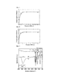
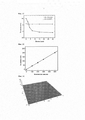
Фигура 1 и Фигура 2 соответственно показывают скорости роста тонких пленок в зависимости от введенных количеств первого прекурсора и второго прекурсора в одном примере настоящего изобретения.Figure 1 and Figure 2 respectively show the growth rates of thin films depending on the amounts of the first precursor and the second precursor introduced in one example of the present invention.
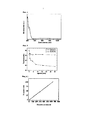
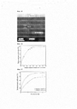
Фигура 3 показывает результаты исследования ультрафиолетовой спектроскопии в отношении органической-неорганической гибридной тонкой пленки и 4-меркаптофенола, изготовленных в одном примере настоящего изобретения.Figure 3 shows the results of an ultraviolet spectroscopy study with respect to an organic-inorganic hybrid thin film and 4-mercaptophenol prepared in one example of the present invention.
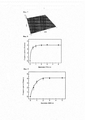
Фигура 4 показывает результаты спектров поглощения в УФ и видимой области исследования в отношении органической-неорганической гибридной тонкой пленке, изготовленной в одном примере настоящего изобретения.Figure 4 shows the results of the absorption spectra in the UV and visible regions of research in relation to the organic-inorganic hybrid thin film made in one example of the present invention.
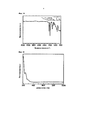
Фигура 5 показывает результаты испытания стабильности на воздухе в отношении органической-неорганической гибридной тонкой пленки, изготовленной в одном примере настоящего изобретения, и тонкой пленки, изготовленной в сравнительном примере.Figure 5 shows the results of an air stability test for an organic-inorganic hybrid thin film made in one example of the present invention and a thin film made in comparative example.
Фигура 6 показывает результаты исследования толщины тонкой пленки в зависимости от цикла процесса формирования органической-неорганической гибридной тонкой пленки в одном примере настоящего изобретения.Figure 6 shows the results of a study of the thickness of a thin film depending on the cycle of the process of forming an organic-inorganic hybrid thin film in one example of the present invention.
Фигура 7 показывает результаты исследования шероховатости поверхности на гибридной тонкой пленке, изготовленной в одном примере настоящего изобретения.Figure 7 shows the results of a surface roughness study on a hybrid thin film made in one example of the present invention.
Фигура 8 и Фигура 9, соответственно, показывают скорости роста тонкой пленки в зависимости от введенных количеств первого прекурсора и второго прекурсора в одном примере настоящего изобретения.Figure 8 and Figure 9, respectively, show the growth rates of a thin film depending on the amounts of the first precursor and the second precursor introduced in one example of the present invention.
Фигура 10 показывает результаты исследования ультрафиолетовой спектроскопии в отношении органической-неорганической гибридной тонкой пленки, изготовленной в одном примере настоящего изобретения.Figure 10 shows the results of an ultraviolet spectroscopy study with respect to an organic-inorganic hybrid thin film made in one example of the present invention.
Фигура 11 показывает результаты исследования спектров поглощения в УФ и видимой области в отношении органической-неорганической гибридной тонкой пленки, изготовленной в одном примере настоящего изобретения.Figure 11 shows the results of the study of the absorption spectra in the UV and visible region in relation to the organic-inorganic hybrid thin film made in one example of the present invention.
Фигура 12 показывает результаты испытания стабильности на воздухе в отношении органической-неорганической гибридной тонкой пленки, изготовленной в одном примере настоящего изобретения, и тонкой пленки, изготовленной в сравнительном примере.Figure 12 shows the results of an air stability test for an organic-inorganic hybrid thin film made in one example of the present invention and a thin film made in comparative example.
Фигура 13 показывает результаты исследования толщины тонкой пленки органической-неорганической гибридной тонкой пленки в результате процесса формирования в одном примере настоящего изобретения.Figure 13 shows the results of studying the thickness of a thin film of an organic-inorganic hybrid thin film as a result of the formation process in one example of the present invention.
Фигура 14 показывает результаты исследования шероховатости поверхности на гибридной тонкой пленке, изготовленной в одном примере настоящего изобретения.Figure 14 shows the results of a surface roughness study on a hybrid thin film made in one example of the present invention.
Фигура 15 показывает результаты исследования посредством ПЭМ (просвечивающей электронной микроскопии) в отношении органической-неорганической гибридной тонкопленочной сверхрешетки, изготовленной в одном примере настоящего изобретения.Figure 15 shows the results of a TEM (Transmission Electron Microscopy) study on an organic-inorganic hybrid thin-film superlattice made in one example of the present invention.
Фигура 16 и Фигура 17 показывают скорость замедления образования точечных дефектов, которую исследовали с помощью изменения толщины органической-неорганической гибридной тонкой пленки в органической-неорганической гибридной тонкопленочной сверхрешетке, изготовленной в одном примере настоящего изобретения.Figure 16 and Figure 17 show the rate of slowing down the formation of point defects, which was investigated by changing the thickness of the organic-inorganic hybrid thin film in the organic-inorganic hybrid thin-film superlattice made in one example of the present invention.
Фигура 18 показывает результаты исследования напряжения тонкой пленки в зависимости от соотношения тонкой пленки Al2O3, образованной с помощью атомно-слоевого осаждения, к органической-неорганической гибридной тонкой пленке в органической-неорганической гибридной тонкопленочной сверхрешетке, изготовленной в одном примере настоящего изобретения.Figure 18 shows the results of studying the voltage of a thin film as a function of the ratio of the Al 2 O 3 thin film formed by atomic layer deposition to an organic-inorganic hybrid thin film in an organic-inorganic hybrid thin-film superlattice made in one example of the present invention.
Фигура 19 показывает результаты в отношении приблизительного окисления органической-неорганической гибридной тонкой пленки, изготовленной в одном примере настоящего изобретения, и тонкой пленки, изготовленной в сравнительном примере.Figure 19 shows the results with respect to the approximate oxidation of an organic-inorganic hybrid thin film made in one example of the present invention and a thin film made in comparative example.
Характерные детали осуществления изобретениеThe characteristic details of the implementation of the invention
Настоящее изобретение дополнительно подробно описано ниже в соответствии с примерами настоящего изобретения. Тем не менее, настоящее изобретение приведенными ниже Примерами не ограничивается.The present invention is further described in detail below in accordance with examples of the present invention. However, the present invention is not limited to the Examples below.
<Пример 1><Example 1>
После того, как подложка Si (100) была промыта с использованием дистиллированной воды и ацетона, ее 2-3 раза продували с использованием газа N2 для того, чтобы удалить какие-либо загрязнения на поверхности подложки, перед тем, как применять диэтилцинк (ДЭZn) в качестве первого соединения прекурсора для наслаивания на подложку Si тонкой пленки диэтилцинка (ДЭZn), в соответствии с методом молекулярного наслаивания.After the Si (100) substrate was washed with distilled water and acetone, it was flushed 2-3 times with N 2 gas in order to remove any contaminants on the substrate surface before applying diethylzinc (DEZn ) as the first precursor compound for layering a thin film of diethyl zinc (DEZn) on a Si substrate, in accordance with the molecular layering method.
Для изготовления органической-неорганической гибридной тонкой пленки, над тонкой пленкой диэтилцинка (ДЭZn) была образована органическая молекулярная пленка, посредством применения 4-меркаптофенола в качестве второго соединения прекурсора, в соответствии с методом молекулярного наслаивания. Аргон применяли как в качестве несущего газа, так и в качестве продувочного газа, и ДЭZn и 4-меркаптофенол, соответственно, испаряли при температуре 20°С и 70°С. Одного цикла достигали с помощью воздействия R3Zn на протяжении 2 секунд, продувая с использованием Ar на протяжении 10 секунд, воздействия 4-меркаптофенола на протяжении 2 секунд и продувания с использованием Ar на протяжении 50 секунд. Тонкая пленка была выращена при температуре, которая составляла 80°С - 200°С, и давлении 300 мТорр.For the manufacture of an organic-inorganic hybrid thin film, an organic molecular film was formed over diethylzinc (DEZn) thin film by using 4-mercaptophenol as the second precursor compound, in accordance with the molecular layering method. Argon was used both as a carrier gas and as a purge gas, and DEZn and 4-mercaptophenol, respectively, were evaporated at a temperature of 20 ° C and 70 ° C. One cycle was achieved by exposure to R3Zn for 2 seconds, blowing with Ar for 10 seconds, exposure to 4-mercaptophenol for 2 seconds, and blowing with Ar for 50 seconds. A thin film was grown at a temperature that was 80 ° C - 200 ° C and a pressure of 300 mTorr.
<Эксперимент> Исследование скорости роста в зависимости от времени введения органического прекурсора и неорганического прекурсора<Experiment> Investigation of growth rate depending on the time of introduction of organic precursor and inorganic precursor
В Примере 1, были исследованы скорости роста тонкой пленки в соответствии с временем введения первого соединения прекурсора диэтилцинка (ДЭZn) и скорости роста тонкой пленки в соответствии с временем введения второго соединения прекурсора 4-меркаптофенола и, соответственно, показаны на Фигуре 1 и Фигуре 2.In Example 1, the growth rate of the thin film was investigated in accordance with the time of introduction of the first compound of the precursor of diethyl zinc (DEZn) and the growth rate of the thin film in accordance with the time of introduction of the second compound of the precursor 4-mercaptophenol and, respectively, are shown in Figure 1 and Figure 2.
Можно заметить на Фигуре 1 и Фигуре 2, что скорости роста тонких пленок увеличиваются с введением определенных количеств первого соединения прекурсора диэтилцинка (ДЭZn) и второго соединения прекурсора 4-меркаптофенола, и затем скорости роста больше не увеличиваются, а остаются при определенных значениях.You can see in Figure 1 and Figure 2 that the growth rates of thin films increase with the introduction of certain amounts of the first compound of the precursor of diethyl zinc (DEZn) and the second compound of the precursor of 4-mercaptophenol, and then the growth rates no longer increase, but remain at certain values.
<Эксперимент> ИК-спектроскопическое исследование<Experiment> IR Spectroscopy
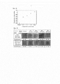
ИК-спектроскопическое исследования выполняли в отношении органической-неорганической гибридной тонкой пленки, изготовленной с помощью такого же способа, как и в Примере 1, за исключением того, что вместо подложки Si и 4-меркаптофенола применяли гранулы KBr, и результаты показаны на Фигуре 3.IR spectroscopic studies were performed on an organic-inorganic hybrid thin film made using the same method as in Example 1, except that KBr granules were used instead of the Si substrate and 4-mercaptophenol, and the results are shown in Figure 3.
Можно удостовериться на Фигуре 3, что гидроксильную группу и тиольную группу 4-меркаптофенола выявляют в сравнительном Примере, где включен только 4-меркаптофенол, в то время как в случае органической-неорганической гибридной тонкой пленки в соответствии с настоящим изобретением, гидроксильную группу и тиольную группу меркаптофенола, который применяют в качестве второго прекурсора, вступающего в реакцию с неорганическим молекулярным слоем, полученным с помощью первого прекурсора, с образованием гибридной тонкой пленки, с помощью метода ИК-спектроскопии не обнаруживают.You can verify in Figure 3 that the hydroxyl group and thiol group of 4-mercaptophenol are detected in comparative example, where only 4-mercaptophenol is included, while in the case of the organic-inorganic hybrid thin film according to the present invention, the hydroxyl group and thiol group mercaptophenol, which is used as the second precursor that reacts with the inorganic molecular layer obtained using the first precursor, to form a hybrid thin film, using the method IR spectroscopy did not show.
<Эксперимент> Спектроскопическое исследование в УФ и видимой области<Experiment> Spectroscopic study in the UV and visible
Исследовали поглощение в УФ и видимой области в отношении органической-неорганической гибридной тонкой пленки, изготовленной в Примере 1 выше, и результаты показаны на Фигуре 4.Investigated the absorption in the UV and the visible region in relation to the organic-inorganic hybrid thin film made in Example 1 above, and the results are shown in Figure 4.
Можно удостовериться на Фигуре 4, что органическая-неорганическая гибридная тонкая пленка в соответствии с настоящим изобретением не имеет поглощения в диапазоне видимого излучения.You can verify in Figure 4 that the organic-inorganic hybrid thin film in accordance with the present invention has no absorption in the range of visible radiation.
<Сравнительный Пример><Comparative Example>
В сравнительном примере органическую-неорганическую гибридную тонкую пленку изготавливали таким же способом, как и в Примере 1 выше, за исключением того, что диэтилцинк (ДЭZn) применяли в качестве первого соединения прекурсора для наслаивания тонкой пленки диэтилцинка (ДЭZn) на подложку Si в соответствии с методом молекулярного наслаивания, и затем в качестве второго соединения прекурсора применяли гидрохинон (HQ).In a comparative example, an organic-inorganic hybrid thin film was made in the same manner as in Example 1 above, except that diethylzinc (DEZn) was used as the first precursor compound for layering a thin film of diethylzinc (DEZn) on a Si substrate in accordance with by molecular layering, and then hydroquinone (HQ) was used as the second precursor compound.
<Эксперимент> Испытание стабильности на воздухе<Experiment> Air Stability Test
В то время как органическую-неорганическую гибридную тонкую пленку Примера 1 и органическую-неорганическую гибридную тонкую пленку, изготовленную в сравнительном примере выше, оставляли на воздухе, в процессе испытания стабильности на воздухе были исследованы изменения их толщины, и результаты показаны на Фигуре 5.While the organic-inorganic hybrid thin film of Example 1 and the organic-inorganic hybrid thin film made in the comparative example above were left in the air, changes in their thickness were examined during the stability test in air, and the results are shown in Figure 5.
Как можно увидеть на Фигуре 5, в отличие от настоящего изобретения, толщина резко уменьшается в случае Сравнительного Примера, который не включает S группу, в то время как, в случае Примера в соответствии с настоящим изобретением, толщина с течением времени не изменяется, и при этом органическая-неорганическая гибридная многослойная пленка, которая включает S группу, является очень стабильной на воздухе.As can be seen in Figure 5, in contrast to the present invention, the thickness decreases dramatically in the case of the Comparative Example, which does not include the S group, while, in the case of the Example in accordance with the present invention, the thickness does not change over time, and This organic-inorganic hybrid multilayer film, which includes the S group, is very stable in air.
<Пример 2><Example 2>
Как и в Примере 1 выше, диэтилцинк (ДЭZn) применяли в качестве первого соединения прекурсора для наслаивания тонкой пленки на подложку Si, и 4-меркаптофенол применяли в качестве второго соединения прекурсора для образования органической-неорганической гибридной тонкой пленки над тонкой пленкой диэтилцинка (ДЭZn) в соответствии с методом молекулярного наслаивания, до процесса образования диэтилцинка (ДЭZn) с помощью первого соединения прекурсора, и когда тонкую пленку, основанную на втором соединении прекурсора, формировали повторно, исследовали толщину тонкой пленки, и результаты показаны на Фигуре 6.As in Example 1 above, diethyl zinc (DEZn) was used as the first precursor compound for lamination of a thin film on a Si substrate, and 4-mercaptophenol was used as the second precursor compound to form an organic-inorganic hybrid thin film over a thin film of diethyl zinc (DEZn) in accordance with the molecular layering method, before the formation of diethyl zinc (DEZn) using the first precursor compound, and when a thin film based on the second precursor compound was re-formed, examine thin film thickness was measured, and the results are shown in Figure 6.
Можно удостовериться на Фигуре 6, что количество повторений в процессе образования тонкой пленки с помощью первого соединения прекурсора и образования тонкой пленки с помощью второго соединения прекурсора является пропорциональным толщине образованной тонкой пленки.You can verify in Figure 6 that the number of repetitions in the process of formation of a thin film using the first connection of the precursor and the formation of a thin film using the second connection of the precursor is proportional to the thickness of the formed thin film.
<Эксперимент> Исследование шероховатости поверхности<Experiment> Investigation of surface roughness
Органическую-неорганическую гибридную тонкую пленку 50 нм толщиной, изготовленную в Примере 2, исследовали в отношении ее шероховатости поверхности, с использованием АСМ (атомного силового микроскопа), и результаты показаны на Фигуре 7. Среднее значение установленной шероховатости составляло 2,2 А.An organic-inorganic hybrid 50 nm thick thin film made in Example 2 was examined for its surface roughness using an AFM (atomic force microscope), and the results are shown in Figure 7. The average value of the established roughness was 2.2 A.
<Пример 3><Example 3>
После того, как подложка Si (100) была промыта с использованием дистиллированной воды и ацетона, ее 2-3 раза продували с использованием газа N2 для того, чтобы удалить какие-либо загрязнения на поверхности подложки, перед тем, как применять триметилалюминий (ТМА) в качестве первого соединения прекурсора для наслаивания тонкой пленки триметилалюминия (ТМА) на подложку Si в соответствии с методом молекулярного наслаивания.After the Si (100) substrate was washed with distilled water and acetone, it was flushed 2-3 times with N 2 gas in order to remove any impurities on the substrate surface before using trimethyl aluminum (TMA ) as the first precursor compound for layering a trimethylaluminum (TMA) thin film on a Si substrate in accordance with the molecular layering method.
Для изготовления органической-неорганической гибридной тонкой пленки, над тонкой пленкой триметилалюминия (ТМА) была образована органическая молекулярная пленка с помощью применения 4-меркаптофенола в качестве второго соединения прекурсора, в соответствии с методом молекулярного наслаивания.For the manufacture of an organic-inorganic hybrid thin film, an organic molecular film was formed over a trimethylaluminum (TMA) thin film by using 4-mercaptophenol as the second precursor compound, in accordance with the molecular layering method.
Аргон применяли как в качестве несущего газа, так и в качестве продувочного газа, и ДЭZn и 4-меркаптофенол, соответственно, испаряли при температуре 20°С и 70°С. Одного цикла достигали с помощью воздействия ДЭZn на протяжении 2 секунд, продувая с использованием Ar на протяжении 10 секунд, воздействия 4-меркаптофенола на протяжении 2 секунд и продувания с использованием Ar на протяжении 50 секунд. Тонкая пленка была выращена при температуре, которая составляла 80°С-200°С, и давлении 300 мТорр.Argon was used both as a carrier gas and as a purge gas, and DEZn and 4-mercaptophenol, respectively, were evaporated at a temperature of 20 ° C and 70 ° C. One cycle was achieved by exposure to DZn for 2 seconds, blowing with Ar for 10 seconds, exposure to 4-mercaptophenol for 2 seconds and blowing with Ar for 50 seconds. A thin film was grown at a temperature of 80 ° C-200 ° C and a pressure of 300 mTorr.
<Эксперимент> Исследование скорости роста в зависимости от времени введения органического прекурсора и неорганического прекурсора<Experiment> Investigation of growth rate depending on the time of introduction of organic precursor and inorganic precursor
В Примере 3, были исследованы скорости роста тонкой пленки в соответствии с временем введения первого соединения прекурсора триметилалюминия (ТМА) и скорости роста тонкой пленки в соответствии с временем введения второго соединения прекурсора 4-меркаптофенола и, соответственно, показаны на Фигуре 8 и Фигуре 9.In Example 3, the growth rates of the thin film were investigated in accordance with the time of introduction of the first trimethylaluminum precursor compound (TMA) and the growth rate of the thin film in accordance with the time of introduction of the second precursor compound 4-mercaptophenol and, respectively, are shown in Figure 8 and Figure 9.
На Фигуре 8 и Фигуре 9 можно заметить, что скорости роста тонких пленок увеличиваются с введением определенных количеств первого соединения прекурсора триметилалюминия (ТМА) и второго соединения прекурсора 4-меркаптофенола, и затем скорости роста больше не увеличиваются, а остаются при определенных значениях.In Figure 8 and Figure 9, it can be seen that the growth rates of thin films increase with the introduction of certain amounts of the first trimethylaluminum precursor compound (TMA) and the second precursor compound 4-mercaptophenol, and then the growth rates no longer increase, but remain at certain values.
<Эксперимент> ИК-спектроскопическое исследование<Experiment> IR Spectroscopy
ИК-спектроскопическое исследования выполняли в отношении органической-неорганической гибридной тонкой пленки, изготовленной с помощью такого же способа, как и в Примере 3, за исключением того, что вместо подложки Si и 4-меркаптофенола применяли гранулы KBr, и результаты показаны на Фигуре 10.IR spectroscopic studies were performed on an organic-inorganic hybrid thin film made using the same method as in Example 3, except that KBr granules were used instead of the Si substrate and 4-mercaptophenol, and the results are shown in Figure 10.
Из Фигуры 10 можно удостовериться, что в случае органической-неорганической гибридной тонкой пленки в соответствии с настоящим изобретением, гидроксильная группа и тиольная группа меркаптофенола, который применяют в качестве второго прекурсора, вступают в реакцию с неорганическим молекулярным слоем, полученным с помощью первого прекурсора, с образованием гибридной тонкой пленки, так, что гидроксильную группу и тиольную группу меркаптофенола с помощью ИК-спектроскопии не обнаруживают.From Figure 10, it can be verified that in the case of the organic-inorganic hybrid thin film according to the present invention, the hydroxyl group and thiol group of the mercaptophenol, which is used as the second precursor, react with the inorganic molecular layer obtained with the first precursor, the formation of a hybrid thin film, so that the hydroxyl group and thiol group of mercaptophenol using IR spectroscopy is not detected.
<Эксперимент> Спектроскопическое исследование в УФ и видимой области<Experiment> Spectroscopic study in the UV and visible
Исследовали поглощение в УФ и видимой области в отношении органической-неорганической гибридной тонкой пленки, изготовленной в Пример 3 выше, и результаты показаны на Фигуре 11.Investigated the absorption in the UV and visible region in relation to organic-inorganic hybrid thin film made in Example 3 above, and the results are shown in Figure 11.
Можно удостовериться из Фигуры 11, что органическая-неорганическая гибридная тонкая пленка в соответствии с настоящим изобретением не имеет поглощения в диапазоне видимого излучения.You can verify from Figure 11 that the organic-inorganic hybrid thin film in accordance with the present invention has no absorption in the range of visible radiation.
<Сравнительный Пример><Comparative Example>
В сравнительном Примере органическую-неорганическую гибридную тонкую пленку получали таким же способом, как и в Примере 3 выше, за исключением того, что триметилалюминий (ТМА) применяли в качестве первого соединения прекурсора для наслаивания тонкой пленки триметилалюминий (ТМА) на подложку Si в соответствии с методом молекулярного наслаивания, и затем в качестве второго соединения прекурсора применяли гидрохинон (HQ).In Comparative Example, an organic-inorganic hybrid thin film was prepared in the same manner as in Example 3 above, except that trimethyl aluminum (TMA) was used as the first precursor compound for layering a trimethyl aluminum (TMA) thin film on a Si substrate in accordance with by molecular layering, and then hydroquinone (HQ) was used as the second precursor compound.
<Эксперимент> Испытание стабильности на воздухе<Experiment> Air Stability Test
В то время как органическую-неорганическую гибридную тонкую пленку Примера 3 и органическую-неорганическую гибридную тонкую пленку, изготовленную в сравнительном Примере выше, оставляли на воздухе, в процессе испытания стабильности на воздухе исследовали изменения в их толщины, и результаты показаны на Фигуре 12.While the organic-inorganic hybrid thin film of Example 3 and the organic-inorganic hybrid thin film made in comparative Example above were left in the air, changes in their thickness were examined during the stability test in air, and the results are shown in Figure 12.
На Фигуре 12 можно увидеть, что, при условии, что начальная толщина составляет d0 и толщина через n часов составляет dn, dn/d0 в случае Сравнительного Примера без включения S группы увеличивается до 0,5 или больше в результате резкого уменьшения толщины, в отличие от настоящего изобретения, при том, что в случае Примера в соответствии с настоящим изобретением, dn/d0 поддерживается на значении 0,1 или меньше в результате отсутствия изменений толщины с течением времени, и при этом органическая-неорганическая гибридная тонкая пленка в соответствии с настоящим изобретением является очень стабильной на воздухе.In Figure 12 it can be seen that, provided that the initial thickness is d0 and the thickness after n hours is dn, dn / d0 in the case of Comparative Example without the inclusion of the S group increases to 0.5 or more as a result of a sharp decrease in thickness, in contrast from the present invention, while in the case of the Example in accordance with the present invention, dn / d0 is maintained at a value of 0.1 or less as a result of the absence of thickness changes over time, while the organic-inorganic hybrid thin film is in accordance with the present The ingenious invention is very stable in air.
<Пример 4><Example 4>
Как и в Примере 3 выше, триметилалюминий (ТМА) применяли в качестве первого соединения прекурсора для наслаивания тонкой пленки над подложкой Si, и 4-меркаптофенол применяли в качестве второго соединения прекурсора для образования органической-неорганической гибридной тонкой пленки над тонкой пленкой триметилалюминия (ТМА) в соответствии с методом молекулярного наслаивания, до процесса образования тонкой пленки триметилалюминия (ТМА) с помощью первого соединения прекурсора, и когда тонкая пленка, основанная на втором соединении прекурсора была образована повторно, исследовали толщину тонкой пленки, и результаты показаны на Фигуре 13.As in Example 3 above, trimethylaluminum (TMA) was used as the first precursor compound for lamination of a thin film over a Si substrate, and 4-mercaptophenol was used as the second precursor compound for the formation of an organic-inorganic hybrid thin film over a trimethylaluminum (TMA) thin film in accordance with the molecular layering method, before the formation of a trimethylaluminum (TMA) thin film using the first precursor compound, and when a thin film based on the second precursor compound pa was re-formed, the thickness of the thin film was investigated, and the results are shown in Figure 13.
Можно удостовериться из Фигуры 13, что количество повторений в процессе образования тонкой пленки с помощью первого соединения прекурсора и образования тонкой пленки с помощью второго соединения прекурсора является пропорциональным толщине полученной тонкой пленки.You can verify from Figure 13 that the number of repetitions in the process of formation of a thin film using the first connection of the precursor and the formation of a thin film using the second connection of the precursor is proportional to the thickness of the obtained thin film.
<Эксперимент> Исследование шероховатости поверхности<Experiment> Investigation of surface roughness
Органическую-неорганическую гибридную тонкую пленку 50 нм толщиной, изготовленную в Примере 4, исследовали в отношении ее шероховатости поверхности, с использованием АСМ, и результаты показаны на Фигуре 14. Среднее значение установленной шероховатости составляло 2,8 А.An organic-inorganic hybrid thin film of 50 nm thick made in Example 4 was examined for its surface roughness using AFM and the results are shown in Figure 14. The average value of the installed roughness was 2.8 A.
<Пример 5><Example 5>
После того, как органическую-неорганическую гибридную тонкую пленку получали таким же способом, как и в Примерах 1 и 3 выше, тонкую пленку Al2O3 наслаивали на органическую-неорганическую гибридную тонкую пленку в соответствии со способом атомно-слоевого осаждения, и указанный способ повторяли, регулируя соотношение тонкой пленки Al2O3, полученной в соответствии с атомно-слоевым осаждением, к органической-неорганической гибридной тонкой пленке в соответствии с настоящим изобретением, для того чтобы получить органическую-неорганическую гибридную функциональную тонкую пленку.After the organic-inorganic hybrid thin film was prepared in the same manner as in Examples 1 and 3 above, a thin film of Al 2 O 3 was layered onto an organic-inorganic hybrid thin film according to the atomic layer deposition method, and this method was repeated, adjusting the ratio of a thin film of Al 2 O 3 produced according to the atomic layer deposition, to the organic-inorganic hybrid thin film according to the present invention, in order to obtain an organic-inorganic g bridnuyu functional thin film.
Для того чтобы получить тонкую пленку Al2O3 в соответствии с осаждением атомных слоев, газ аргон применяли в качестве несущего газа и продувочного газа, и при этом триметилалюминий (ТМА) и Н2О испаряли при стандартной температуре. Цикл достигали с помощью воздействия ТМА на протяжении 1 секунды, продувая с использованием Ar на протяжении 5 секунд, воздействия Н2О на протяжении 1 секунды и продувания с использованием Ar на протяжении 5 секунд. Упомянутая выше тонкая пленка была выращена при температуре, которая составляла 80°С, и давлении 300 мТорр.In order to obtain a thin film of Al 2 O 3 in accordance with the deposition of atomic layers, argon gas was used as carrier gas and purge gas, and trimethyl aluminum (TMA) and H 2 O were evaporated at standard temperature. The cycle was achieved using TMA for 1 second, blowing with Ar for 5 seconds, H 2 O for 1 second and blowing with Ar for 5 seconds. The thin film mentioned above was grown at a temperature of 80 ° C and a pressure of 300 mTorr.
<Эксперимент> ПЭМ-исследование<Experiment> TEM Study
Фотографирование с помощью ПЭМ осуществляли, когда соотношение органической-неорганической гибридной тонкой пленки к тонкой пленке Al2O3, изготовленной в Пример 5 выше, составляло 1:2, и при этом результаты показаны на Фигуре 15. Можно удостовериться из Фигуры 15, что тонкая пленка Al2O3 в соответствии с осаждением атомных слоев и органическая-неорганическая гибридная тонкая пленка в соответствии с настоящим изобретением были попеременно образованы.Photographing with TEM was performed when the ratio of organic-inorganic hybrid thin film to Al 2 O 3 thin film made in Example 5 above was 1: 2, and the results are shown in Figure 15. You can verify from Figure 15 that the thin an Al 2 O 3 film in accordance with the deposition of atomic layers and an organic-inorganic hybrid thin film in accordance with the present invention were alternately formed.
<Эксперимент> Исследование действия замедления образования точечных дефектов<Experiment> Investigation of the effect of slowing the formation of point defects
В Примере 5 выше, были исследованы скорости замедления образования точечных дефектов с помощью изменения толщины органической-неорганической гибридной тонкой пленки, и результаты показаны на Фигуре 16 и Фигуре 17.In Example 5 above, the rate of slowing down the formation of point defects was investigated by changing the thickness of the organic-inorganic hybrid thin film, and the results are shown in Figure 16 and Figure 17.
Как можно увидеть на Фигуре 16, точечные дефекты образуются редко, если толщина органической-неорганической гибридной тонкой пленки в соответствии с настоящим изобретением составляет 80 нм или более.As can be seen in Figure 16, point defects are rarely formed if the thickness of the organic-inorganic hybrid thin film in accordance with the present invention is 80 nm or more.
<Эксперимент> Исследование напряжений тонкой пленки<Experiment> Examination of thin film stresses
В органической-неорганической гибридной функциональной тонкой пленке, изготовленной в Примере 5 выше, исследовали напряжения тонкой пленки в зависимости от соотношения тонкой пленки Al2O3 к органической-неорганической гибридной тонкой пленке в соответствии с настоящим изобретением, в то время как общую толщину тонкой пленки поддерживали одинаковой, и результаты показаны на Фигуре 18.In the organic-inorganic hybrid functional thin film made in Example 5 above, the stresses of the thin film were investigated depending on the ratio of the Al 2 O 3 thin film to the organic-inorganic hybrid thin film in accordance with the present invention, while the total thickness of the thin film maintained the same, and the results are shown in Figure 18.
<Эксперимент> Исследования устойчивости к проникновению влаги и устойчивости к проникновению кислорода<Experiment> Studies of resistance to moisture penetration and resistance to oxygen penetration
Органическую-неорганическую гибридную функциональную тонкую пленку, изготовленную в Пример 5 выше, и тонкую пленку Al2O3 Сравнительного Примера исследовали в отношении устойчивости к проникновению влаги и устойчивости к проникновению кислорода, и результаты показаны в Таблице 1 и на Фигуре 19 ниже.The organic-inorganic hybrid functional thin film made in Example 5 above and the Al 2 O 3 thin film of Comparative Example were examined for resistance to moisture penetration and resistance to oxygen penetration, and the results are shown in Table 1 and in Figure 19 below.
Можно заметить из Таблицы 1 и Фигуре 19 ниже, что функциональная тонкая пленка, содержащая органическую-неорганическую гибридную тонкую пленку и Al2O3 в соответствии с настоящим изобретением, имеет превосходную устойчивость к проникновению влаги и устойчивость к проникновению кислорода, по сравнению с пленкой Сравнительного Примера.It can be seen from Table 1 and Figure 19 below that a functional thin film containing an organic-inorganic hybrid thin film and Al 2 O 3 in accordance with the present invention has excellent resistance to moisture penetration and resistance to oxygen penetration, as compared to a film of Comparative Example.

Промышленная ПрименимостьIndustrial Applicability
По той причине, что органическая-неорганическая гибридная тонкая пленка и покрывающая пленка в соответствии с настоящим изобретением включают новую функциональную группу, так, что они остаются стабильными на воздухе, указанные пленки могут применяться в различные областях, включая наноструктурирование для изготовления полупроводников и электронных устройств, химических датчиков и биосенсоров, в сфере разработок нанотрибологии, поверхностных модификаций, наноэлектронных машинных систем (NEMS), микроэлектронных машинных систем (MEMS) и в энергонезависимых запоминающих устройствах.Because the organic-inorganic hybrid thin film and coating film in accordance with the present invention includes a new functional group so that they remain stable in air, these films can be used in various fields, including nanostructuring for the manufacture of semiconductors and electronic devices, chemical sensors and biosensors in the development of nanotribology, surface modifications, nanoelectronic machine systems (NEMS), microelectronic machine systems (MEMS) and nergonezavisimyh storage devices.
Способ изготовления органической-неорганической гибридной тонкой пленки в соответствии с настоящим изобретением позволяет обеспечить очень стабильную на воздухе органическую-неорганическую гибридную многослойную молекулярную пленку, посредством включения в органический прекурсор новой функциональной группы, которую не применяли раньше, во время изготовления органической-неорганической гибридной тонкой пленки, где попеременно применяют неорганический прекурсор и органический прекурсор в соответствии с методом молекулярного наслаивания.The method of manufacturing an organic-inorganic hybrid thin film in accordance with the present invention makes it possible to provide a very stable in air organic-inorganic hybrid multilayer molecular film by incorporating into the organic precursor a new functional group that was not used before, during the manufacture of an organic-inorganic hybrid thin film where an inorganic precursor and an organic precursor are alternately used in accordance with the molecular method laivaniya.
Claims (41)


Applications Claiming Priority (3)
| Application Number | Priority Date | Filing Date | Title |
|---|---|---|---|
| KR1020130104463 | 2013-08-30 | ||
| KR10-2013-0104463 | 2013-08-30 | ||
| PCT/KR2013/009909 WO2015030297A1 (en) | 2013-08-30 | 2013-11-04 | Hybrid organic/inorganic thin films and method of manufacturing same |
Publications (2)
| Publication Number | Publication Date |
|---|---|
| RU2016111693A RU2016111693A (en) | 2017-10-06 |
| RU2670303C2 true RU2670303C2 (en) | 2018-10-22 |
Family
ID=52586830
Family Applications (2)
| Application Number | Title | Priority Date | Filing Date |
|---|---|---|---|
| RU2016111694A RU2672962C2 (en) | 2013-08-30 | 2013-11-04 | Substrate structure and method for manufacture thereof |
| RU2016111693A RU2670303C2 (en) | 2013-08-30 | 2013-11-04 | Functional thin film and method of its manufacture |
Family Applications Before (1)
| Application Number | Title | Priority Date | Filing Date |
|---|---|---|---|
| RU2016111694A RU2672962C2 (en) | 2013-08-30 | 2013-11-04 | Substrate structure and method for manufacture thereof |
Country Status (12)
| Country | Link |
|---|---|
| US (2) | US10418300B2 (en) |
| EP (2) | EP3040443B1 (en) |
| JP (2) | JP6286557B2 (en) |
| KR (2) | KR20150026746A (en) |
| CN (2) | CN105723011B (en) |
| BR (2) | BR112016004389B1 (en) |
| CA (2) | CA2922615A1 (en) |
| MX (2) | MX2016002433A (en) |
| RU (2) | RU2672962C2 (en) |
| SG (2) | SG11201600923YA (en) |
| TW (2) | TWI521083B (en) |
| WO (2) | WO2015030298A1 (en) |
Families Citing this family (20)
| Publication number | Priority date | Publication date | Assignee | Title |
|---|---|---|---|---|
| US10418300B2 (en) * | 2013-08-30 | 2019-09-17 | Iucf-Hyu (Industry-University Cooperation Foundation Hanyang University | Substrate structure and method for preparing the same |
| TWI538276B (en) * | 2013-09-30 | 2016-06-11 | Lg化學股份有限公司 | Substrate for organic electronic device and manufacturing method thereof |
| BR112016028225B1 (en) | 2014-06-12 | 2022-08-16 | Basf Coatings Gmbh | PROCESS FOR PRODUCTION OF A LAMINATED, LAMINATED, PROTECTIVE FILM, USE OF A PROTECTIVE FILM AND ELECTRONIC DEVICE |
| SG11201707265QA (en) * | 2015-03-25 | 2017-10-30 | Basf Coatings Gmbh | Process for producing flexible organic-inorganic laminates |
| WO2017141870A1 (en) * | 2016-02-18 | 2017-08-24 | シャープ株式会社 | Method for producing organic el display device, and organic el display device |
| KR102586045B1 (en) * | 2016-07-12 | 2023-10-10 | 삼성디스플레이 주식회사 | Display apparatus and manufacturing method thereof |
| US20190040503A1 (en) * | 2017-08-03 | 2019-02-07 | Hrl Laboratories, Llc | Feedstocks for additive manufacturing, and methods of using the same |
| WO2019010696A1 (en) * | 2017-07-14 | 2019-01-17 | General Electric Company | A method of gas-phase molecular layer-by-layer deposition on a microporous support |
| US10673046B2 (en) * | 2018-04-13 | 2020-06-02 | GM Global Technology Operations LLC | Separator for lithium metal based batteries |
| EP3818192A1 (en) * | 2018-07-05 | 2021-05-12 | BASF Coatings GmbH | Transparent conductive film |
| KR102224346B1 (en) * | 2019-07-11 | 2021-03-05 | 한양대학교 산학협력단 | Organic-inorganic hybrid layer, organic-inorganic laminate having the layer, organic electroinc device including the laminate as a gas barrier |
| CN110508155B (en) * | 2019-08-21 | 2021-09-03 | 南京大学 | Preparation method of zinc-based inorganic-organic hybrid nano porous separation membrane |
| CN110635044B (en) * | 2019-11-04 | 2021-07-06 | 吉林大学 | Composite packaging film of organic metal halide perovskite solar cell and preparation method thereof |
| CN112410763A (en) * | 2020-10-28 | 2021-02-26 | 武汉华星光电半导体显示技术有限公司 | Thin film packaging layer, preparation method thereof and foldable display device |
| TWI824213B (en) * | 2020-12-19 | 2023-12-01 | 逢甲大學 | Flexible transparent conductive composite films and method of manufacturing the same |
| KR102558965B1 (en) * | 2021-03-18 | 2023-07-25 | 한국과학기술연구원 | Stretchable disply device and manufacturing method thereof |
| EP4334380A1 (en) | 2021-05-06 | 2024-03-13 | BASF Coatings GmbH | Multilayer barrier film, its manufacture and use in photovoltaic applications |
| WO2023018308A1 (en) * | 2021-08-12 | 2023-02-16 | 한양대학교 산학협력단 | Multi-layered molecular film photoresist having molecular line structure and method for manufacturing same |
| CN115124727B (en) * | 2022-07-08 | 2023-07-14 | 中国科学院山西煤炭化学研究所 | Preparation method of MOF film |
| CN117845191A (en) * | 2022-09-30 | 2024-04-09 | 华为技术有限公司 | Composite film and preparation method and application thereof |
Citations (5)
| Publication number | Priority date | Publication date | Assignee | Title |
|---|---|---|---|---|
| US20080102313A1 (en) * | 2004-12-28 | 2008-05-01 | Universitetet I Oslo | Thin Films Prepared With Gas Phase Deposition Technique |
| US20090081883A1 (en) * | 2007-09-26 | 2009-03-26 | Freeman Diane C | Process for depositing organic materials |
| US20100178481A1 (en) * | 2007-06-22 | 2010-07-15 | George Steven M | Protective coatings for organic electronic devices made using atomic layer deposition and molecular layer deposition techniques |
| RU2462793C2 (en) * | 2007-12-28 | 2012-09-27 | Юниверсите Де Ля Медитерране Экс-Марсель Ii | Hybrid nanocomposite materials |
| WO2012157960A2 (en) * | 2011-05-16 | 2012-11-22 | 주식회사 엘지화학 | Multi-layer plastic substrate and method for manufacturing same |
Family Cites Families (39)
| Publication number | Priority date | Publication date | Assignee | Title |
|---|---|---|---|---|
| JPH05220106A (en) | 1992-02-14 | 1993-08-31 | Olympus Optical Co Ltd | Endoscope photographing system |
| RU2118402C1 (en) * | 1994-05-17 | 1998-08-27 | Виктор Васильевич Дроботенко | Method of preparing metal oxide coatings (variants thereof) |
| JP2002053669A (en) * | 2000-06-01 | 2002-02-19 | Osaka Organic Chem Ind Ltd | Multidimensional organic-inorganic complex compound and method for producing the same |
| US6866949B2 (en) | 2002-03-08 | 2005-03-15 | Dai Nippon Printing Co., Ltd. | Substrate film, gas barrier film, and display using the same |
| TW548853B (en) * | 2002-09-13 | 2003-08-21 | Ind Tech Res Inst | Method of manufacturing flexible TFT display |
| US7285440B2 (en) * | 2002-11-25 | 2007-10-23 | International Business Machines Corporation | Organic underlayers that improve the performance of organic semiconductors |
| JP2004231784A (en) * | 2003-01-30 | 2004-08-19 | Konica Minolta Holdings Inc | Organic-inorganic polymer hybrid film, its preparation method, and display and touch panel using said film |
| US7229703B2 (en) | 2003-03-31 | 2007-06-12 | Dai Nippon Printing Co. Ltd. | Gas barrier substrate |
| JP4654911B2 (en) | 2003-05-16 | 2011-03-23 | 凸版印刷株式会社 | Transparent gas barrier laminated film, electroluminescence light emitting device, electroluminescence display device, and electrophoretic display panel using the same |
| US20050153077A1 (en) | 2003-12-03 | 2005-07-14 | Anthony Gedeon | Method of resisting contaminant build up and oxidation of vehicle surfaces and other surfaces |
| JP2005289885A (en) * | 2004-03-31 | 2005-10-20 | Osaka Organic Chem Ind Ltd | Multidimensional organic-inorganic composite compound, composite burnt product and methods for producing these |
| JP2005297498A (en) | 2004-04-16 | 2005-10-27 | Dainippon Printing Co Ltd | Flexible base board, and organic device using the same |
| US7378157B2 (en) | 2004-06-28 | 2008-05-27 | Dai Nippon Printing Co., Ltd. | Gas barrier film, and display substrate and display using the same |
| KR101001441B1 (en) * | 2004-08-17 | 2010-12-14 | 삼성전자주식회사 | Organic-Inorganic Metal Hybrid Material and Organic Insulator Composition Comprising the Same |
| JP2007185937A (en) | 2005-12-12 | 2007-07-26 | Fujifilm Corp | Organic-inorganic hybrid material, gas barrier film and its manufacturing method |
| KR20070084683A (en) * | 2006-02-21 | 2007-08-27 | 국민대학교산학협력단 | Molecular layer deposition |
| JP2007273094A (en) | 2006-03-30 | 2007-10-18 | Toppan Printing Co Ltd | Organic electroluminescence element and manufacturing method therefor |
| DE102006016280A1 (en) * | 2006-04-01 | 2007-10-04 | Pvflex Solar Gmbh | Glassless thin-film solar power module, has solar cell in starting, inorganic barrier layer, inorganic-organic hybrid polymer barrier layer, transparent adhesive layer and cover film in front side and adhesive layer in rear side |
| JP2008087163A (en) | 2006-09-29 | 2008-04-17 | Fujifilm Corp | Gas barrier laminated film and image display element using it |
| KR101449076B1 (en) | 2006-11-13 | 2015-02-23 | 더 리젠츠 오브 더 유니버시티 오브 콜로라도, 어 바디 코포레이트 | Molecular layer deposition process for making organic or organic-inorganic polymers |
| JP2008218632A (en) * | 2007-03-02 | 2008-09-18 | Fujifilm Corp | Electronic device |
| WO2008117487A1 (en) | 2007-03-23 | 2008-10-02 | Dai Nippon Printing Co., Ltd. | Gas barrier sheet |
| JP5127277B2 (en) | 2007-04-05 | 2013-01-23 | 新日鉄住金マテリアルズ株式会社 | Surface flatness insulating film forming coating solution, surface flatness insulating film coated base material, and method for producing surface flatness insulating film coated base material |
| JP5198131B2 (en) | 2007-05-14 | 2013-05-15 | 富士フイルム株式会社 | Barrier film and element |
| US7947377B2 (en) | 2007-06-20 | 2011-05-24 | Dai Nippon Printing Co., Ltd. | Powder mixture to be made into evaporation source material for use in ion plating, evaporation source material for use in ion plating and method of producing the same, and gas barrier sheet and method of producing the same |
| US20090021797A1 (en) * | 2007-07-17 | 2009-01-22 | Luciano Joseph W | All-In-One Device With Integrated Monitor |
| JP2010006039A (en) | 2007-09-05 | 2010-01-14 | Fujifilm Corp | Gas barrier film, and method for sealing display element using gas barrier film |
| US8067085B2 (en) | 2007-09-14 | 2011-11-29 | Fujifilm Corporation | Gas barrier film, and display device comprising the same |
| US8776238B2 (en) * | 2008-07-16 | 2014-07-08 | International Business Machines Corporation | Verifying certificate use |
| US8241749B2 (en) | 2008-09-11 | 2012-08-14 | Fujifilm Corporation | Barrier laminate, gas barrier film, and device using the same |
| JP2011046060A (en) | 2009-08-26 | 2011-03-10 | Fujifilm Corp | Gas barrier film and method for manufacturing gas barrier film |
| JP4821925B2 (en) | 2009-11-27 | 2011-11-24 | 大日本印刷株式会社 | GAS BARRIER FILM, DEVICE, AND METHOD FOR PRODUCING GAS BARRIER FILM |
| EP2549560B1 (en) * | 2010-03-17 | 2018-09-26 | Konica Minolta Holdings, Inc. | Organic electronic device and method of manufacturing the same |
| JP5772814B2 (en) | 2010-03-25 | 2015-09-02 | 凸版印刷株式会社 | Gas barrier laminate and packaging material |
| JP5598080B2 (en) | 2010-05-17 | 2014-10-01 | 大日本印刷株式会社 | Method for producing gas barrier sheet |
| JP5913809B2 (en) | 2011-01-05 | 2016-04-27 | リンテック株式会社 | Transparent electrode substrate, method for producing the same, electronic device having the transparent electrode substrate, and solar cell |
| JP5752438B2 (en) | 2011-02-23 | 2015-07-22 | グンゼ株式会社 | Gas barrier film |
| KR101432737B1 (en) | 2011-07-28 | 2014-08-22 | 한양대학교 산학협력단 | Hybrid organic-inorganic thin film and producing method of the same |
| US10418300B2 (en) * | 2013-08-30 | 2019-09-17 | Iucf-Hyu (Industry-University Cooperation Foundation Hanyang University | Substrate structure and method for preparing the same |
-
2013
- 2013-11-04 US US14/915,562 patent/US10418300B2/en active Active
- 2013-11-04 WO PCT/KR2013/009910 patent/WO2015030298A1/en active Application Filing
- 2013-11-04 MX MX2016002433A patent/MX2016002433A/en unknown
- 2013-11-04 EP EP13892719.9A patent/EP3040443B1/en active Active
- 2013-11-04 CN CN201380079150.XA patent/CN105723011B/en active Active
- 2013-11-04 SG SG11201600923YA patent/SG11201600923YA/en unknown
- 2013-11-04 JP JP2016538482A patent/JP6286557B2/en active Active
- 2013-11-04 EP EP13892196.0A patent/EP3040442B1/en active Active
- 2013-11-04 WO PCT/KR2013/009909 patent/WO2015030297A1/en active Application Filing
- 2013-11-04 JP JP2016538483A patent/JP6654753B2/en active Active
- 2013-11-04 RU RU2016111694A patent/RU2672962C2/en active
- 2013-11-04 CA CA2922615A patent/CA2922615A1/en not_active Abandoned
- 2013-11-04 BR BR112016004389-8A patent/BR112016004389B1/en active IP Right Grant
- 2013-11-04 CN CN201380079249.XA patent/CN105745353B/en active Active
- 2013-11-04 RU RU2016111693A patent/RU2670303C2/en active
- 2013-11-04 MX MX2016002432A patent/MX2016002432A/en unknown
- 2013-11-04 US US14/413,754 patent/US9576876B2/en active Active
- 2013-11-04 BR BR112016004476A patent/BR112016004476A2/en not_active Application Discontinuation
- 2013-11-04 CA CA2922612A patent/CA2922612A1/en not_active Abandoned
- 2013-11-04 SG SG11201600921XA patent/SG11201600921XA/en unknown
- 2013-12-02 TW TW102144000A patent/TWI521083B/en active
- 2013-12-02 TW TW102143967A patent/TWI606111B/en active
-
2014
- 2014-02-17 KR KR20140018154A patent/KR20150026746A/en not_active Application Discontinuation
- 2014-02-18 KR KR1020140018212A patent/KR102289064B1/en active IP Right Grant
Patent Citations (5)
| Publication number | Priority date | Publication date | Assignee | Title |
|---|---|---|---|---|
| US20080102313A1 (en) * | 2004-12-28 | 2008-05-01 | Universitetet I Oslo | Thin Films Prepared With Gas Phase Deposition Technique |
| US20100178481A1 (en) * | 2007-06-22 | 2010-07-15 | George Steven M | Protective coatings for organic electronic devices made using atomic layer deposition and molecular layer deposition techniques |
| US20090081883A1 (en) * | 2007-09-26 | 2009-03-26 | Freeman Diane C | Process for depositing organic materials |
| RU2462793C2 (en) * | 2007-12-28 | 2012-09-27 | Юниверсите Де Ля Медитерране Экс-Марсель Ii | Hybrid nanocomposite materials |
| WO2012157960A2 (en) * | 2011-05-16 | 2012-11-22 | 주식회사 엘지화학 | Multi-layer plastic substrate and method for manufacturing same |
Non-Patent Citations (2)
| Title |
|---|
| KATSUHIKO KANAIZUKA et al. "Construction of Highly Oriented Crystalline Surface Coordination Polymers Composed of Copper Dithiooxamide Complexes", J. AM. CHEM. SOC., v. 130(47), 2008, p. 15778-15779. * |
| MATHIAS BRUST et al. "Self-assembly of photoluminescent copper(I)-dithiol multilayer thin films and bulk materials", LANGMUIR, v. 13(21), 1997, p. 5602-5607. * |
Also Published As
Similar Documents
| Publication | Publication Date | Title |
|---|---|---|
| RU2670303C2 (en) | Functional thin film and method of its manufacture | |
| Hackley et al. | Properties of atomic layer deposited HfO2 thin films | |
| Malm et al. | Atomic layer deposition of WO3 thin films using W (CO) 6 and O3 precursors | |
| Mar et al. | Factors influencing the chemical vapor deposition of oriented ZnO films using zinc acetate | |
| US11352692B2 (en) | Hexagonal boron nitride thin film and method for producing the same | |
| Al-Dulaimi et al. | The influence of precursor on rhenium incorporation into Re-doped MoS 2 (Mo 1− x Re x S 2) thin films by aerosol-assisted chemical vapour deposition (AACVD) | |
| Kayani et al. | Structural, optical, and magnetic properties of cobalt-doped dip coated ZnO films | |
| Riaz et al. | Effect of Mn-doping concentration on the structural & magnetic properties of sol-gel deposited ZnO diluted magnetic semiconductor | |
| KR20150026747A (en) | Organic inorganic hybrid thin films and method for preparing the same | |
| Wang et al. | Chemical solution deposition of ZnO thin films with controlled crystallite orientation and intense ultraviolet emission | |
| Imperia et al. | XMCD studies of Cox Pt100–x nanoparticles prepared by vapour deposition and chemical synthesis | |
| JP2015017022A (en) | Method for producing graphene | |
| KR100416504B1 (en) | Manganese-doped ferromagnetic zinc oxide and method of manufacturing the same | |
| TWI385117B (en) | Production Method of ZnO Nanometer Structure by Liquid Chromatography | |
| Du et al. | Synthesis of Ga-riched zinc gallate nanowires by reactive evaporation and the cathodoluminescence properties of individual nanowires | |
| Sivakumar et al. | Characterisation of the Magnetic property of the Cobalt (Transition metal) doped with Zinc Oxide using Spin Coating Technique | |
| Xin et al. | Study on the effect of Sn concentration on the structural, optical, and electrical properties of (Al 0.55 In 0.45) 2 O 3: Sn films | |
| Ding et al. | Thermal stability studies on ion beam sputter deposited substoichiometric iron nitride thin films | |
| Guglieri Rodríguez et al. | Synthesis and In-house Characterization of Materials | |
| KR20180072363A (en) | Fabrication Method for Insulation Layer of Semiconductor Device by ECR-ALD |
Legal Events
| Date | Code | Title | Description |
|---|---|---|---|
| PC41 | Official registration of the transfer of exclusive right |
Effective date: 20200311 |