RU2633103C2 - Methods for display with double modulation with light transformation - Google Patents
Methods for display with double modulation with light transformation Download PDFInfo
- Publication number
- RU2633103C2 RU2633103C2 RU2015137943A RU2015137943A RU2633103C2 RU 2633103 C2 RU2633103 C2 RU 2633103C2 RU 2015137943 A RU2015137943 A RU 2015137943A RU 2015137943 A RU2015137943 A RU 2015137943A RU 2633103 C2 RU2633103 C2 RU 2633103C2
- Authority
- RU
- Russia
- Prior art keywords
- light
- backlight
- display
- pixel
- converting
- Prior art date
Links
- 238000000034 method Methods 0.000 title claims description 32
- 230000009466 transformation Effects 0.000 title 1
- 238000004088 simulation Methods 0.000 claims abstract description 21
- 230000005284 excitation Effects 0.000 claims abstract description 18
- 239000002096 quantum dot Substances 0.000 claims abstract description 17
- 230000003595 spectral effect Effects 0.000 claims description 20
- 239000011159 matrix material Substances 0.000 claims description 7
- 238000005286 illumination Methods 0.000 claims description 6
- 230000005855 radiation Effects 0.000 claims description 4
- 230000000694 effects Effects 0.000 abstract description 7
- 239000000126 substance Substances 0.000 abstract 1
- 230000003287 optical effect Effects 0.000 description 21
- 238000006243 chemical reaction Methods 0.000 description 19
- 238000004891 communication Methods 0.000 description 14
- 230000006870 function Effects 0.000 description 11
- OAICVXFJPJFONN-UHFFFAOYSA-N Phosphorus Chemical compound [P] OAICVXFJPJFONN-UHFFFAOYSA-N 0.000 description 8
- 239000003086 colorant Substances 0.000 description 6
- 238000013500 data storage Methods 0.000 description 6
- 238000001228 spectrum Methods 0.000 description 6
- 241001600434 Plectroglyphidodon lacrymatus Species 0.000 description 5
- 238000013459 approach Methods 0.000 description 5
- 230000005540 biological transmission Effects 0.000 description 5
- 239000000463 material Substances 0.000 description 5
- 238000012986 modification Methods 0.000 description 4
- 230000004048 modification Effects 0.000 description 4
- 230000008901 benefit Effects 0.000 description 3
- 238000010586 diagram Methods 0.000 description 3
- 230000009977 dual effect Effects 0.000 description 3
- 238000005516 engineering process Methods 0.000 description 3
- 230000010287 polarization Effects 0.000 description 3
- 239000004065 semiconductor Substances 0.000 description 3
- 235000012431 wafers Nutrition 0.000 description 3
- 238000003491 array Methods 0.000 description 2
- 230000008859 change Effects 0.000 description 2
- 239000004973 liquid crystal related substance Substances 0.000 description 2
- 238000004519 manufacturing process Methods 0.000 description 2
- 230000007246 mechanism Effects 0.000 description 2
- 230000008569 process Effects 0.000 description 2
- 238000012545 processing Methods 0.000 description 2
- 239000007787 solid Substances 0.000 description 2
- 230000003068 static effect Effects 0.000 description 2
- 238000012546 transfer Methods 0.000 description 2
- RYGMFSIKBFXOCR-UHFFFAOYSA-N Copper Chemical compound [Cu] RYGMFSIKBFXOCR-UHFFFAOYSA-N 0.000 description 1
- 241000276699 Seriola Species 0.000 description 1
- 238000007792 addition Methods 0.000 description 1
- 230000004075 alteration Effects 0.000 description 1
- 238000009529 body temperature measurement Methods 0.000 description 1
- 239000000969 carrier Substances 0.000 description 1
- 230000015556 catabolic process Effects 0.000 description 1
- 239000004020 conductor Substances 0.000 description 1
- 238000006731 degradation reaction Methods 0.000 description 1
- 230000001419 dependent effect Effects 0.000 description 1
- 238000000295 emission spectrum Methods 0.000 description 1
- 239000000284 extract Substances 0.000 description 1
- 239000000835 fiber Substances 0.000 description 1
- 238000010438 heat treatment Methods 0.000 description 1
- 239000002105 nanoparticle Substances 0.000 description 1
- 238000000206 photolithography Methods 0.000 description 1
- 238000007639 printing Methods 0.000 description 1
- 238000009877 rendering Methods 0.000 description 1
Images
Classifications
-
- G—PHYSICS
- G09—EDUCATION; CRYPTOGRAPHY; DISPLAY; ADVERTISING; SEALS
- G09G—ARRANGEMENTS OR CIRCUITS FOR CONTROL OF INDICATING DEVICES USING STATIC MEANS TO PRESENT VARIABLE INFORMATION
- G09G3/00—Control arrangements or circuits, of interest only in connection with visual indicators other than cathode-ray tubes
- G09G3/20—Control arrangements or circuits, of interest only in connection with visual indicators other than cathode-ray tubes for presentation of an assembly of a number of characters, e.g. a page, by composing the assembly by combination of individual elements arranged in a matrix no fixed position being assigned to or needed to be assigned to the individual characters or partial characters
- G09G3/34—Control arrangements or circuits, of interest only in connection with visual indicators other than cathode-ray tubes for presentation of an assembly of a number of characters, e.g. a page, by composing the assembly by combination of individual elements arranged in a matrix no fixed position being assigned to or needed to be assigned to the individual characters or partial characters by control of light from an independent source
- G09G3/3406—Control of illumination source
- G09G3/3413—Details of control of colour illumination sources
-
- G—PHYSICS
- G09—EDUCATION; CRYPTOGRAPHY; DISPLAY; ADVERTISING; SEALS
- G09G—ARRANGEMENTS OR CIRCUITS FOR CONTROL OF INDICATING DEVICES USING STATIC MEANS TO PRESENT VARIABLE INFORMATION
- G09G3/00—Control arrangements or circuits, of interest only in connection with visual indicators other than cathode-ray tubes
- G09G3/20—Control arrangements or circuits, of interest only in connection with visual indicators other than cathode-ray tubes for presentation of an assembly of a number of characters, e.g. a page, by composing the assembly by combination of individual elements arranged in a matrix no fixed position being assigned to or needed to be assigned to the individual characters or partial characters
- G09G3/22—Control arrangements or circuits, of interest only in connection with visual indicators other than cathode-ray tubes for presentation of an assembly of a number of characters, e.g. a page, by composing the assembly by combination of individual elements arranged in a matrix no fixed position being assigned to or needed to be assigned to the individual characters or partial characters using controlled light sources
- G09G3/30—Control arrangements or circuits, of interest only in connection with visual indicators other than cathode-ray tubes for presentation of an assembly of a number of characters, e.g. a page, by composing the assembly by combination of individual elements arranged in a matrix no fixed position being assigned to or needed to be assigned to the individual characters or partial characters using controlled light sources using electroluminescent panels
- G09G3/32—Control arrangements or circuits, of interest only in connection with visual indicators other than cathode-ray tubes for presentation of an assembly of a number of characters, e.g. a page, by composing the assembly by combination of individual elements arranged in a matrix no fixed position being assigned to or needed to be assigned to the individual characters or partial characters using controlled light sources using electroluminescent panels semiconductive, e.g. using light-emitting diodes [LED]
-
- G—PHYSICS
- G09—EDUCATION; CRYPTOGRAPHY; DISPLAY; ADVERTISING; SEALS
- G09G—ARRANGEMENTS OR CIRCUITS FOR CONTROL OF INDICATING DEVICES USING STATIC MEANS TO PRESENT VARIABLE INFORMATION
- G09G3/00—Control arrangements or circuits, of interest only in connection with visual indicators other than cathode-ray tubes
- G09G3/20—Control arrangements or circuits, of interest only in connection with visual indicators other than cathode-ray tubes for presentation of an assembly of a number of characters, e.g. a page, by composing the assembly by combination of individual elements arranged in a matrix no fixed position being assigned to or needed to be assigned to the individual characters or partial characters
- G09G3/34—Control arrangements or circuits, of interest only in connection with visual indicators other than cathode-ray tubes for presentation of an assembly of a number of characters, e.g. a page, by composing the assembly by combination of individual elements arranged in a matrix no fixed position being assigned to or needed to be assigned to the individual characters or partial characters by control of light from an independent source
- G09G3/3406—Control of illumination source
- G09G3/342—Control of illumination source using several illumination sources separately controlled corresponding to different display panel areas, e.g. along one dimension such as lines
- G09G3/3426—Control of illumination source using several illumination sources separately controlled corresponding to different display panel areas, e.g. along one dimension such as lines the different display panel areas being distributed in two dimensions, e.g. matrix
-
- G—PHYSICS
- G09—EDUCATION; CRYPTOGRAPHY; DISPLAY; ADVERTISING; SEALS
- G09G—ARRANGEMENTS OR CIRCUITS FOR CONTROL OF INDICATING DEVICES USING STATIC MEANS TO PRESENT VARIABLE INFORMATION
- G09G3/00—Control arrangements or circuits, of interest only in connection with visual indicators other than cathode-ray tubes
- G09G3/20—Control arrangements or circuits, of interest only in connection with visual indicators other than cathode-ray tubes for presentation of an assembly of a number of characters, e.g. a page, by composing the assembly by combination of individual elements arranged in a matrix no fixed position being assigned to or needed to be assigned to the individual characters or partial characters
- G09G3/34—Control arrangements or circuits, of interest only in connection with visual indicators other than cathode-ray tubes for presentation of an assembly of a number of characters, e.g. a page, by composing the assembly by combination of individual elements arranged in a matrix no fixed position being assigned to or needed to be assigned to the individual characters or partial characters by control of light from an independent source
- G09G3/36—Control arrangements or circuits, of interest only in connection with visual indicators other than cathode-ray tubes for presentation of an assembly of a number of characters, e.g. a page, by composing the assembly by combination of individual elements arranged in a matrix no fixed position being assigned to or needed to be assigned to the individual characters or partial characters by control of light from an independent source using liquid crystals
-
- H—ELECTRICITY
- H05—ELECTRIC TECHNIQUES NOT OTHERWISE PROVIDED FOR
- H05B—ELECTRIC HEATING; ELECTRIC LIGHT SOURCES NOT OTHERWISE PROVIDED FOR; CIRCUIT ARRANGEMENTS FOR ELECTRIC LIGHT SOURCES, IN GENERAL
- H05B45/00—Circuit arrangements for operating light-emitting diodes [LED]
- H05B45/20—Controlling the colour of the light
- H05B45/24—Controlling the colour of the light using electrical feedback from LEDs or from LED modules
-
- G—PHYSICS
- G02—OPTICS
- G02F—OPTICAL DEVICES OR ARRANGEMENTS FOR THE CONTROL OF LIGHT BY MODIFICATION OF THE OPTICAL PROPERTIES OF THE MEDIA OF THE ELEMENTS INVOLVED THEREIN; NON-LINEAR OPTICS; FREQUENCY-CHANGING OF LIGHT; OPTICAL LOGIC ELEMENTS; OPTICAL ANALOGUE/DIGITAL CONVERTERS
- G02F1/00—Devices or arrangements for the control of the intensity, colour, phase, polarisation or direction of light arriving from an independent light source, e.g. switching, gating or modulating; Non-linear optics
- G02F1/01—Devices or arrangements for the control of the intensity, colour, phase, polarisation or direction of light arriving from an independent light source, e.g. switching, gating or modulating; Non-linear optics for the control of the intensity, phase, polarisation or colour
- G02F1/13—Devices or arrangements for the control of the intensity, colour, phase, polarisation or direction of light arriving from an independent light source, e.g. switching, gating or modulating; Non-linear optics for the control of the intensity, phase, polarisation or colour based on liquid crystals, e.g. single liquid crystal display cells
- G02F1/133—Constructional arrangements; Operation of liquid crystal cells; Circuit arrangements
- G02F1/1333—Constructional arrangements; Manufacturing methods
- G02F1/1335—Structural association of cells with optical devices, e.g. polarisers or reflectors
- G02F1/1336—Illuminating devices
- G02F1/133601—Illuminating devices for spatial active dimming
-
- G—PHYSICS
- G02—OPTICS
- G02F—OPTICAL DEVICES OR ARRANGEMENTS FOR THE CONTROL OF LIGHT BY MODIFICATION OF THE OPTICAL PROPERTIES OF THE MEDIA OF THE ELEMENTS INVOLVED THEREIN; NON-LINEAR OPTICS; FREQUENCY-CHANGING OF LIGHT; OPTICAL LOGIC ELEMENTS; OPTICAL ANALOGUE/DIGITAL CONVERTERS
- G02F1/00—Devices or arrangements for the control of the intensity, colour, phase, polarisation or direction of light arriving from an independent light source, e.g. switching, gating or modulating; Non-linear optics
- G02F1/01—Devices or arrangements for the control of the intensity, colour, phase, polarisation or direction of light arriving from an independent light source, e.g. switching, gating or modulating; Non-linear optics for the control of the intensity, phase, polarisation or colour
- G02F1/13—Devices or arrangements for the control of the intensity, colour, phase, polarisation or direction of light arriving from an independent light source, e.g. switching, gating or modulating; Non-linear optics for the control of the intensity, phase, polarisation or colour based on liquid crystals, e.g. single liquid crystal display cells
- G02F1/133—Constructional arrangements; Operation of liquid crystal cells; Circuit arrangements
- G02F1/1333—Constructional arrangements; Manufacturing methods
- G02F1/1335—Structural association of cells with optical devices, e.g. polarisers or reflectors
- G02F1/1336—Illuminating devices
- G02F1/133614—Illuminating devices using photoluminescence, e.g. phosphors illuminated by UV or blue light
-
- G—PHYSICS
- G02—OPTICS
- G02F—OPTICAL DEVICES OR ARRANGEMENTS FOR THE CONTROL OF LIGHT BY MODIFICATION OF THE OPTICAL PROPERTIES OF THE MEDIA OF THE ELEMENTS INVOLVED THEREIN; NON-LINEAR OPTICS; FREQUENCY-CHANGING OF LIGHT; OPTICAL LOGIC ELEMENTS; OPTICAL ANALOGUE/DIGITAL CONVERTERS
- G02F2202/00—Materials and properties
- G02F2202/36—Micro- or nanomaterials
-
- G—PHYSICS
- G09—EDUCATION; CRYPTOGRAPHY; DISPLAY; ADVERTISING; SEALS
- G09G—ARRANGEMENTS OR CIRCUITS FOR CONTROL OF INDICATING DEVICES USING STATIC MEANS TO PRESENT VARIABLE INFORMATION
- G09G2310/00—Command of the display device
- G09G2310/02—Addressing, scanning or driving the display screen or processing steps related thereto
- G09G2310/0237—Switching ON and OFF the backlight within one frame
-
- G—PHYSICS
- G09—EDUCATION; CRYPTOGRAPHY; DISPLAY; ADVERTISING; SEALS
- G09G—ARRANGEMENTS OR CIRCUITS FOR CONTROL OF INDICATING DEVICES USING STATIC MEANS TO PRESENT VARIABLE INFORMATION
- G09G2320/00—Control of display operating conditions
- G09G2320/02—Improving the quality of display appearance
- G09G2320/0233—Improving the luminance or brightness uniformity across the screen
-
- G—PHYSICS
- G09—EDUCATION; CRYPTOGRAPHY; DISPLAY; ADVERTISING; SEALS
- G09G—ARRANGEMENTS OR CIRCUITS FOR CONTROL OF INDICATING DEVICES USING STATIC MEANS TO PRESENT VARIABLE INFORMATION
- G09G2320/00—Control of display operating conditions
- G09G2320/02—Improving the quality of display appearance
- G09G2320/0242—Compensation of deficiencies in the appearance of colours
-
- G—PHYSICS
- G09—EDUCATION; CRYPTOGRAPHY; DISPLAY; ADVERTISING; SEALS
- G09G—ARRANGEMENTS OR CIRCUITS FOR CONTROL OF INDICATING DEVICES USING STATIC MEANS TO PRESENT VARIABLE INFORMATION
- G09G3/00—Control arrangements or circuits, of interest only in connection with visual indicators other than cathode-ray tubes
- G09G3/20—Control arrangements or circuits, of interest only in connection with visual indicators other than cathode-ray tubes for presentation of an assembly of a number of characters, e.g. a page, by composing the assembly by combination of individual elements arranged in a matrix no fixed position being assigned to or needed to be assigned to the individual characters or partial characters
- G09G3/34—Control arrangements or circuits, of interest only in connection with visual indicators other than cathode-ray tubes for presentation of an assembly of a number of characters, e.g. a page, by composing the assembly by combination of individual elements arranged in a matrix no fixed position being assigned to or needed to be assigned to the individual characters or partial characters by control of light from an independent source
- G09G3/3406—Control of illumination source
- G09G3/342—Control of illumination source using several illumination sources separately controlled corresponding to different display panel areas, e.g. along one dimension such as lines
Landscapes
- Engineering & Computer Science (AREA)
- Physics & Mathematics (AREA)
- Computer Hardware Design (AREA)
- General Physics & Mathematics (AREA)
- Theoretical Computer Science (AREA)
- Chemical & Material Sciences (AREA)
- Crystallography & Structural Chemistry (AREA)
- Liquid Crystal Display Device Control (AREA)
- Control Of Indicators Other Than Cathode Ray Tubes (AREA)
- Liquid Crystal (AREA)
- Devices For Indicating Variable Information By Combining Individual Elements (AREA)
Abstract
Description
Перекрестные ссылки на родственные заявкиCross references to related applications
[0001] Настоящая заявка испрашивает приоритет согласно предварительной заявке на патент США №61/775375 под названием "Techniques for Dual Modulation Display with Light Conversion", поданной 8 марта 2013 года, содержание которой в полном объеме включено посредством ссылки в данную заявку. Настоящая заявка также связана с совладельцем предварительной заявки на патент США №61/703020 под названием "Quantum Dot/Remote Phosphor Display System Improvements", поданной 19 сентября 2012 года, содержание которой в полном объеме включено в данную заявку посредством ссылки во всех отношениях.[0001] This application claims priority according to provisional application for US patent No. 61/775375 entitled "Techniques for Dual Modulation Display with Light Conversion", filed March 8, 2013, the contents of which are fully incorporated by reference in this application. This application is also associated with the co-owner of provisional application for US patent No. 61/703020 called "Quantum Dot / Remote Phosphor Display System Improvements", filed September 19, 2012, the contents of which are fully incorporated into this application by reference in all respects.
ТехнологииTechnologies
[0002] Настоящее изобретение относится в целом к способам отображения, и, в частности, к способам отображения с двойной модуляцией с преобразованием света.[0002] The present invention relates generally to display methods, and in particular to light modulation dual modulation display methods.
Предпосылки создания изобретенияBACKGROUND OF THE INVENTION
[0003] Массивы цветных фильтров в жидкокристаллических дисплеях (LCD) и органических светодиодных (OLED) дисплеях в большинстве случаев изготавливают посредством технологий фотолитографии или технологий печати, как части процесса производства LCD и OLED панелей. Цветные фильтры в излучающих дисплеях, таких как LCD и OLED дисплеи, как правило, состоят из красных, зеленых и синих фильтров. Цветные фильтры имеют упорядоченную структуру на матрице пикселей для обеспечения возможности пиксельным элементам модулировать излучаемый свет по цвету, а также по интенсивности. В процессе работы широкополосный источник света (например, белого света) подает свет на пиксельные элементы, например, в LCD дисплейных системах. Кроме того, широкополосный свет создается белыми OLED пиксельным элементами в OLED дисплейных системах. Пиксельный элемент может изменять интенсивность широкополосного света, исходящего из пиксельного элемента. Широкополосный свет с модуляцией интенсивности каждого пиксельного элемента может дополнительно фильтроваться по цвету посредством наложения цветных фильтров. Большая часть света используется цветными фильтрами непроизводительно потому что, например, чтобы создать спектр красного света (например, приблизительно 620-740 нанометров), затем спектр зеленого света (например, приблизительно 520-570 нанометров) и спектр синего света (например, приблизительно 450-495 нанометров), широкополосный источник света будет заблокирован. Кроме того, это непроизводительное использование света превращается во вредный нагрев, который ухудшает производительность и срок службы дисплейной системы.[0003] Arrays of color filters in liquid crystal displays (LCD) and organic light emitting diode (OLED) displays are in most cases manufactured by photolithography or printing technologies, as part of the manufacturing process of LCD and OLED panels. Color filters in emitting displays, such as LCD and OLED displays, typically consist of red, green, and blue filters. Color filters have an ordered structure on a matrix of pixels to allow pixel elements to modulate the emitted light in color as well as in intensity. In operation, a broadband light source (e.g., white light) supplies light to pixel elements, for example, in LCD display systems. In addition, broadband light is created by white OLED pixel elements in OLED display systems. The pixel element may vary the intensity of the broadband light emanating from the pixel element. Broadband light with modulation of the intensity of each pixel element can be additionally filtered by color by applying color filters. Most of the light used by color filters is unproductive because, for example, to create a spectrum of red light (e.g., approximately 620-740 nanometers), then a spectrum of green light (e.g., approximately 520-570 nanometers) and a blue light spectrum (e.g., approximately 450- 495 nanometers), the broadband light source will be blocked. In addition, this unproductive use of light turns into harmful heat, which degrades the performance and life of the display system.
[0004] Таким образом, многими производителями дисплеев проектирование дисплейных систем с широкой цветовой гаммой и высокой яркостью было признано дорогостоящим процессом. Из-за большого количества относительно дорогих оптических, звуковых, электронных и механических задействованных компонентов и сложности в интеграции их всех в одной системе, стоимость изготовления дисплейной системы, достойной похвалы, как правило, очень высока.[0004] Thus, by many display manufacturers, designing display systems with a wide color gamut and high brightness has been recognized as an expensive process. Due to the large number of relatively expensive optical, sound, electronic, and mechanical components involved and the difficulty in integrating them all into one system, the cost of manufacturing a display system worthy of praise is usually very high.
[0005] Таким образом, изобретателями в данной заявке установлено, что дисплей с двойной модуляцией с преобразованием света может обеспечить множество функциональных преимуществ по сравнению с традиционными способами, использующими цветовые фильтры, в частности, обеспечить повышение производительности дисплея и исключение вредного нагрева.[0005] Thus, the inventors in this application have found that a dual-modulation display with light conversion can provide many functional advantages compared to traditional methods using color filters, in particular, to increase the performance of the display and eliminate harmful heating.
[0006] Подходы, описанные в этом разделе, являются подходами, которые могут осуществляться, но не обязательно являются подходами, которые были ранее задуманы или осуществлены. Поэтому, если не указано иное, не следует считать, что любой из подходов, описанный в данном разделе, определяется как предшествующий уровень техники только в силу его включения в данный раздел. Аналогичным образом, проблемы, определенные в отношении одного или нескольких подходов, не следует считать общепризнанными в любом предшествующем уровне техники на основании данного раздела, если не указано иное.[0006] The approaches described in this section are approaches that can be implemented, but are not necessarily approaches that have been previously conceived or implemented. Therefore, unless otherwise indicated, it should not be considered that any of the approaches described in this section is defined as prior art only by virtue of its inclusion in this section. Similarly, problems identified in relation to one or more approaches should not be considered generally accepted in any prior art based on this section unless otherwise indicated.
Краткое описание изобретенияSUMMARY OF THE INVENTION
[0007] Предложены способы и устройства для возбуждения дисплея с двойной модуляцией (также упоминаемого в данной заявке как дисплей с локальным затемнением). Источники света излучают первый свет на светопреобразующий слой. Светопреобразующий слой преобразует первый свет во второй свет. Модулирующие сигналы возбуждения для определения прохождения второго света могут регулироваться частично в зависимости от одного или нескольких имитационных моделирований светового поля.[0007] Methods and devices for driving a dual modulation display (also referred to as a local dimming display in this application) are provided. The light sources emit the first light onto the light converting layer. The light conversion layer converts the first light into second light. Modulating excitation signals for determining the passage of the second light can be partially controlled depending on one or more simulation simulations of the light field.
[0008] В одном из вариантов осуществления настоящего изобретения возбуждение дисплея с локальным затемнением включает генерирование сигналов возбуждения подсветки для возбуждения раздельно управляемых источников света. Источники света излучают первый свет на светопреобразующий слой. Светопреобразующий слой преобразует первый свет во второй свет. Светопреобразующий слой может содержать квантовые точки или кристаллические люминофоры. Модулирующие сигналы возбуждения генерируются для определения прохождения второго света через отдельные подпиксели дисплея. Эти модулирующие сигналы возбуждения могут регулироваться в зависимости от одного или нескольких имитационных моделирований светового поля. Имитационные моделирования светового поля могут решать вопросы, связанные с: (i) возникающим цветовым сдвигом для пикселя в зависимости от функции рассеяния точки источников света; (ii) отличающимся процессом биннинга отдельных источников света; (Hi) температурной зависимостью компонентов дисплея от производительности; или (iv) с их сочетаниями.[0008] In one embodiment of the present invention, driving a local dimming display includes generating backlight drive signals for driving separately controlled light sources. The light sources emit the first light onto the light converting layer. The light conversion layer converts the first light into second light. The light converting layer may contain quantum dots or crystalline phosphors. Modulating excitation signals are generated to determine the passage of the second light through the individual sub-pixels of the display. These modulating excitation signals can be adjusted depending on one or more simulation simulations of the light field. Simulations of the light field can solve issues related to: (i) the resulting color shift for a pixel depending on the scattering function of the point of the light sources; (ii) a different binning process for individual light sources; (Hi) temperature dependence of display components on performance; or (iv) with combinations thereof.
[0009] В другом варианте осуществления настоящего изобретения способ для возбуждения дисплея с локальным затемнением включает генерирование в зависимости от данных изображения сигналов возбуждения подсветки для возбуждения раздельно управляемых светодиодных (LED) источников подсветки. Раздельно управляемые светодиодные источники излучают первый свет на слой квантовых точек, который преобразует по меньшей мере часть первого света (а также, факультативно, повторно используемый свет в дисплее) во второй свет. Определяются модулирующие сигналы возбуждения LCD, регулирующие прохождение второго света через отдельные подпиксели дисплея посредством LCD матрицы. Определяется увеличение спектральных составляющих желтого света для пикселя в зависимости от одного или нескольких сигналов возбуждения подсветки и соответствующих расстояний между пикселем и одним или несколькими LED источниками. Модулирующий сигнал возбуждения LCD по меньшей мере для одного подпикселя пикселя регулируется для уменьшения спектральной составляющей желтого света при визуализации пикселя.[0009] In another embodiment of the present invention, a method for driving a local dimming display includes generating, depending on image data, backlight driving signals for driving separately controlled light emitting diode (LED) backlight sources. Separately controlled LED sources emit first light onto a quantum dot layer, which converts at least a portion of the first light (and, optionally, reusable light in the display) into second light. Modulating LCD drive signals are determined that control the passage of the second light through the individual subpixels of the display by means of an LCD matrix. The increase in the spectral components of yellow light for a pixel is determined depending on one or more backlight excitation signals and the corresponding distances between the pixel and one or more LED sources. The modulating LCD drive signal for at least one pixel subpixel is adjusted to reduce the spectral component of yellow light when rendering the pixel.
[0010] В еще одном варианте осуществления настоящего изобретения дисплейная система содержит один или несколько источников света подсветки, выполненных с возможностью излучения первого света. Первый свет может содержать ультрафиолетовые (UV) спектральные составляющие (например, приблизительно 10-400 нанометров) и/или спектральные составляющие синего света. Дисплей дополнительно содержит один или несколько светопреобразующих слоев, выполненных с возможностью возбуждения первым светом и преобразования по меньшей мере части первого света во второй свет. Модуляторы света выполнены с возможностью модулировать количество второго света, проходящего через отдельные пиксели дисплейной системы. Логический блок выполняет одно или несколько имитационных моделирований светового поля для (i) цветового сдвига в зависимости от функции рассеяния точки подсветки, (ii) различия между эксплуатационной характеристикой источника света из одного или нескольких источников света подсветки и эксплуатационной характеристикой подсветки, (iii) колебания температуры для визуализированного пикселя, или их сочетаний. Контроллер может регулировать значения возбуждения для одного или нескольких модуляторов света в зависимости от имитационного моделирования светового поля.[0010] In yet another embodiment of the present invention, the display system comprises one or more backlight sources configured to emit first light. The first light may contain ultraviolet (UV) spectral components (for example, approximately 10-400 nanometers) and / or spectral components of blue light. The display further comprises one or more light converting layers configured to excite the first light and convert at least a portion of the first light into second light. Light modulators are configured to modulate the amount of second light passing through individual pixels of the display system. The logic unit performs one or more simulations of the light field for (i) a color shift depending on the scattering function of the backlight, (ii) the difference between the performance of the light source from one or more backlight sources and the performance of the backlight, (iii) temperature fluctuations for a rendered pixel, or combinations thereof. The controller can adjust the excitation values for one or more light modulators depending on the simulation of the light field.
Краткое описание графического материалаA brief description of the graphic material
[0011] Настоящее изобретение иллюстрируется в качестве примера, а не с целью ограничения, фигурами прилагаемого графического материала, на которых подобные номера позиций относятся к подобным элементам, и на которых:[0011] The present invention is illustrated by way of example, and not for the purpose of limitation, by the figures of the attached graphic material, in which like reference numbers refer to like elements, and in which:
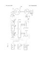
[0012] на фиг. 1 представлена примерная панель цветовой матрицы, содержащая преобразующий слой;[0012] in FIG. 1 shows an exemplary color matrix panel comprising a conversion layer;
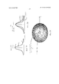
[0013] на фиг. 2А, 2В и 2С представлен пример PSF, имеющей цветовой сдвиг в зависимости от расстояния от центра;[0013] in FIG. 2A, 2B, and 2C show an example of a PSF having a color shift as a function of distance from the center;
[0014] на фиг. 3 представлена примерная конфигурация логического блока дисплея в дисплейной системе;[0014] in FIG. 3 shows an exemplary configuration of a display logic unit in a display system;
[0015] на фиг. 4 представлена примерная блок-схема возбуждения дисплея с локальным затемнением; и[0015] in FIG. 4 is an exemplary block diagram of a local dimming display drive; and
[0016] на фиг. 5 представлена примерная аппаратная платформа, на которой могут реализовываться компьютер или вычислительное устройство, как описано в данной заявке, в соответствии с возможным вариантом осуществления настоящего изобретения.[0016] in FIG. 5 illustrates an exemplary hardware platform on which a computer or computing device may be implemented, as described herein, in accordance with a possible embodiment of the present invention.
Описание примерных возможных вариантов осуществленияDescription of Exemplary Possible Embodiments
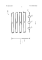
[0017] Нижеследующее описание и графический материал являются поясняющими изобретение и не должны толковаться как ограничивающие изобретение. Описаны многочисленные специфические подробности для обеспечения полного понимания настоящего изобретения. Тем не менее, в некоторых случаях хорошо известные либо общепринятые детали не описаны во избежание затруднения понимания описания изобретения.[0017] The following description and graphic material are illustrative of the invention and should not be construed as limiting the invention. Numerous specific details are described to provide a thorough understanding of the present invention. However, in some cases, well-known or generally accepted details are not described in order to avoid difficulty in understanding the description of the invention.
[0018] На фиг. 1 приведена примерная панель 100 цветовой матрицы, содержащая оптическую стопу 101. Оптическая стопа 101 может без ограничения содержать:[0018] FIG. 1 shows an exemplary
i. преобразующий слой 102;i. a
ii. источники 104 света;ii.
iii. отражающую поверхность 106;iii.
iv. рассеивающий слой 108;iv. a
v. пленку 110 повторного использования света; иv.
vi. слой 112 световой модуляции.vi.
[0019] Преобразующий слой 102, расположенный перед (с точки зрения зрителя) источниками 104 света, может содержать квантовую точку или кристаллические люминофоры. Квантовая точка (например, наночастицы, применяющие для светового излучения квантово-размерный эффект) или кристаллические люминофоры могут покрывать, прикрепляться к, наноситься или иным образом располагаться на верхней поверхности, нижней поверхности или обеих поверхностях оптического слоя для образования преобразующего слоя 102. Квантовая точка или кристаллические люминофоры также могут встраиваться в оптический слой. Данные материалы могут располагаться с оптическим слоем в любом сочетании или порядке различных способов расположения.[0019] The
[0020] Преобразующий слой 102, применяющий цветовые матрицы квантовых точек или люминофорные цветовые матрицы, передает цвета в цветной дисплейной системе. Красная квантовая точка или кристаллический люминофор поглощает свет с более высокими энергиями или более короткими длинами волн, такой как зеленый и синий свет, и излучает красный свет. Зеленая квантовая точка или кристаллический люминофор поглощает синий свет и излучает зеленый свет. Соответственно, в одном варианте осуществления настоящего изобретения преобразующий слой 102 дает желаемые цвета: красный и зеленый свет преобразуется от источника синего света; в то время как синий свет, излучается непосредственно из источника синего света.[0020] The
[0021] В одном из вариантов осуществления настоящего изобретения преобразующий слой 102 представляет собой одинарную пластину (или в альтернативном варианте составную из упорядоченных сегментов с образованием единой плоскости), проходящую по ширине и высоте так, чтобы в основном быть равной размерам рабочей площади устройства отображения. Например, преобразующий слой 102 может измеряться по диагонали: приблизительно 4 дюйма, 10 дюймов, 32 дюйма, 40 дюймов, 50 дюймов, 58 дюймов или больше. Кроме того, преобразующий слой 102 может иметь наряду с прочими соотношение сторон или пропорциональное соотношение между шириной и высотой: 16:9, 4:3, 3:2, 5:3, 5:4 или 1:1. Как показано на фиг. 1, преобразующий слой 102 расположен далеко от источника света 104. В альтернативном варианте осуществления настоящего изобретения преобразующий слой 102 содержит множество сегментов. В конкретном варианте осуществления каждый сегмент из множества сегментов связан с одним источником 104 света.[0021] In one embodiment of the present invention, the
[0022] Источники 104 света могут представлять собой любой источник электромагнитной энергии, пригодный для использования преобразующим слоем 102 для создания видимого света для человека или машинного зрения. Например, источники 104 света могут содержать один или несколько OLED, RGB LED, широкополосных LED, LED синего спектра, LED ультрафиолетового спектра или тому подобное.[0022] The
[0023] Эти источники 104 света могут располагаться в виде матрицы, проходящей по существу по длине и высоте рабочей площади устройства отображения. Плотность шага между источниками 104 света может равняться или соответствовать разрешающей способности дисплея в пикселях. То есть, отношение источников 104 света к количеству пикселей может быть 1:1 (например, 1920×1080, 3840×2160 или 7680×4320 источников света для соответствующего разрешения дисплея). В этом случае положение каждого из источников 104 света может непосредственно совпадать (с точки зрения зрителя) с соответствующим пикселем. В других случаях источники 104 света могут располагаться с боковым смещением от соответствующего пикселя или между двумя пикселями. Шаг между источниками 104 света может быть равномерным или неравномерным, например, плотность шага может быть выше в непосредственной близости к центральной рабочей площади дисплея, чем в периферии, по краям, в углах, или черных полосах в формате "почтовый ящик".[0023] These
[0024] В других вариантах осуществления отношение источников 104 света к числу пикселей может быть ниже, например, 1:2, 1:3, 1:4, 1:10 и более. В этом случае разрешение изображения подсветки будет уменьшено. В альтернативном варианте это отношение может быть выше, например, 2:1, 3:1, или меньше. Например, источник света может быть связан с подпикселем, а не пикселем или группой пикселей.[0024] In other embodiments, the ratio of
[0025] Данные источники 104 света являются раздельно управляемыми или в альтернативном варианте их подмножество может синхронно совместно управляться. Гибкость управления подсветкой посредством раздельно управляемых источников 104 света обеспечивает локальное затемнение. Дополнительные сведения о технологии локального затемнения можно найти в патенте США №8277056 под названием "Locally Dimmed Display", который включен в полном объеме в данную заявку посредством ссылки во всех отношениях. Однако, несмотря на раздельное управление источниками 104 света, PSF каждого источника 104 света может перекрываться, чтобы повлиять на интенсивность множества пикселей.[0025] These
[0026] Хотя на фиг. 1 показан дисплей с прямой подсветкой, дисплей с боковой подсветкой также может пользоваться преимуществами изобретений, сообщенными в данном описании (например, компенсацией для цветового сдвига от PSF, биннингом источников света или колебанием температуры). В таком варианте осуществления пространственный модулятор света освещается одним или несколькими источниками света, расположенными на краю пространственного модулятора света. Дополнительные сведения о боковой подсветке, локальном затемнении можно найти в патенте США №8172401 под названием "Edge Lit Locally Dimmed Display", который в полном объеме включен в данную заявку посредством ссылки во всех отношениях.[0026] Although in FIG. Figure 1 shows a direct-backlit display, a side-lit display can also take advantage of the inventions described herein (e.g., PSF color shift compensation, binning of light sources, or temperature variation). In such an embodiment, the spatial light modulator is illuminated by one or more light sources located at the edge of the spatial light modulator. Additional information about side lighting, local dimming can be found in US patent No. 8172401 called "Edge Lit Locally Dimmed Display", which is fully incorporated into this application by reference in all respects.
[0027] Отражающая поверхность 106 может представлять собой широкополосную зеркальную поверхность, дихроическую зеркальную поверхность, отражающую заданный спектр (например, один или несколько основных цветов). Кроме того, отражающая поверхность 106 может содержать сквозные отверстия для источников 104 света. Эти сквозные отверстия можно растачивать, сверлить или фрезеровать. Отражающая поверхность 106 перенаправляет свет обратно через оптическую стопу 101 для повышения эффективности.[0027] The
[0028] На фиг. 1 рассеивающий слой 108 рассеивает исходящий свет через диапазон направлений таким образом, что зритель, расположенный на противоположной стороне рассеивателя 108 воспринимает свет, как исходящий от увеличенной площади. В общем случае рассеиватель 108 может рассеивать свет до разных угловых размеров в горизонтальной и вертикальной плоскостях.[0028] In FIG. 1, the
[0029] Пленка 110 повторного использования света применяется для увеличения оптической эффективности подсветки. В некоторых вариантах осуществления, поскольку слой 112 световой модуляции может только (или по существу только) пропускать поляризованный свет, а подсветка в основном дает неполяризованный свет. Отражающий поляризатор (например, 3М DBEF) может применяться в качестве последнего оптического слоя до слоя 112 световой модуляции. Свет с неправильной поляризацией, падающий на слой 112 световой модуляции, который в противном случае будет поглощен, отражается обратно пленкой 110 повторного использования света по направлению к подсветке. Отраженный свет будет рассеиваться в рассеивающем слое 108, который придает случайный характер поляризации. Отраженный свет, имеющий поляризацию случайного характера, которая имеет часть правильной поляризации для прохождения через слой 112 световой модуляции, может перенаправляться к слою 112 световой модуляции, поскольку он рассеивает и отражает в оптической стопе.[0029] The
[0030] Другая пленка 110 повторного использования света может представлять собой призматически структурированную пленку (например, 3М BEF), которая применяется для управления направлением света, выходящего из блока подсветки. Чтобы максимизировать интенсивность света в пределах угла обзора слоя 112 световой модуляции, свет за пределами угла обзора может отражаться обратно в оптический резонатор, который после рассеяния и отражения может привести к тому, что часть отраженного света имеет необходимый выходящий угол в пределах угла обзора.[0030] Another
[0031] Слой 112 световой модуляции может содержать, например, (i) LCD панель, которая является примером модулятора света пропускающего типа, (ii) деформируемое зеркальное устройство (DMD), которое является примером модулятора света отражающего типа, или (iii) модулятор на основе микроэлектромеханической системы (MEMS). Элементы модулятора 112 света управляются в соответствии с данными, которые определяют отображаемое изображение.[0031] The
[0032] Следует учитывать, что на фиг. 1 показан вариант осуществления оптической стопы 101, а расположение элементов в ней может варьироваться или может включать дополнительные неописанные элементы. Например, пленка ПО повторного использования света может располагаться за рассеивающим слоем 108, а не перед ним. В качестве еще одного примера преобразующий слой 102 может располагаться в любом месте в пределах оптической стопы 101 после источников 104 света. Все такие модификации и видоизменения предполагаются для включения в объем настоящего изобретения.[0032] Note that in FIG. 1 shows an embodiment of an
[0033] Изобретателями в данной заявке учтено, что примерная панель 100 цветовой матрицы страдает от «эффекта желтого хвоста» или функции рассеяния точки (PSF), которая сдвигает цвета в зависимости от расстояния от центра. То есть, свет, проходящий относительно длинный оптический путь, перенаправленный обратно на пространственные области, близкие к или ближайшие к источникам света, может пространственно распространяться в широких углах и площадях и вызывать цветовые сдвиги (например, желтые хвосты) - в частности, со светом, повторно использующимся посредством одного или нескольких отражений. В такой системе, например, свет в центре функции рассеяния точки излучателя света прямой подсветки будет в основном преобразовываться, но составляющие отраженного света могут отразиться и преобразоваться в менее зеленый и красный, поскольку расстояние от центра функции рассеяния точки излучателя света до внешних окружностей увеличивается, что приводит к цветовому сдвигу, к функции рассеяния точки (PSF). Хвост PSF становится все более и более желтым, даже когда центр PSF содержит желаемую белую точку. Без функции компенсации, ухудшение цветового сдвига может быть особенно значительным или даже зрительно заметным. На фиг. 2А, 2В и 2С в качестве простых иллюстраций показан эффект желтого хвоста.[0033] The inventors in this application have taken into account that an exemplary
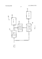
[0034] На фиг. 3 показана примерная конфигурация логического блока дисплея в дисплейной системе 300. В соответствии с некоторыми возможными вариантами осуществления настоящего изобретения дисплейная система 300 содержит логический блок 302 управления подсветкой для управления источниками света в подсветке 304. Эти источники света могут быть таким же или подобными источникам 104 света, показанным на фиг. 1. Логический блок 302 управления подсветкой может функционально соединяться с источником данных изображения (не показан) (например, телевизионной приставкой, сетевым сервером, накопителем данных и тому подобным) и выполнен с возможностью приема данных изображения от источника данных изображения. Кадры изображения, полученные или образованные из данных изображения из внутреннего или внешнего источника, могут использоваться логическим блоком 302 управления подсветкой для управления подсветкой 304. Например, логический блок 302 управления подсветкой может выполняться для управления подсветкой 304 для освещения одного или нескольких пикселей или подпикселей с определенной интенсивностью. Кадры изображения могут использоваться логическим блоком 302 управления подсветкой для получения значений раздельного или совместного возбуждения в различных кадрах при различных разрешениях.[0034] FIG. 3 illustrates an exemplary configuration of a display logic unit in a
[0035] В этом варианте осуществления настоящего изобретения логический блок 302 управления подсветкой логически соединен с логическим блоком 306 имитационного моделирования светового поля. Логический блок 306 имитационного моделирования светового поля вычисляет один или несколько факторов влияния на световое поле, таких как, например, эффект желтого хвоста, биннинга источников света, температурная зависимость от системных компонентов и тому подобное. В зависимости от этих факторов влияния логический блок 306 имитационного моделирования светового поля и/или логический блок 308 управления модулятором (например, логический блок управления LCD панелью) могут уменьшить их для улучшения качества изображения. Например, для уменьшения эффекта желтого хвоста, значения возбуждения модулятора 310 (например, LCD панели) могут быть искажены, чтобы быть более синими.[0035] In this embodiment of the present invention, the backlight
[0036] В одном из вариантов осуществления имитационное моделирование светового поля может использовать девять каналов свертки, представляющих три трехцветных значения цвета для каждого из трех основных цветов. Однако, это требует значительных вычислительных ресурсов. В качестве альтернативы имитационное моделирование светового поля может моделировать раздельно управляемые источники света подсветки, как имеющие первую PSF для спектральных составляющих широкополосного света и вторую PSF для спектральных составляющих желтого света - или два канала сверток, а не девять. Первая PSF является более узкой, чем перекрывающая вторая PSF от эффекта желтого хвоста.[0036] In one embodiment, the simulation of the light field may use nine convolution channels representing three tri-color color values for each of the three primary colors. However, this requires significant computing resources. Alternatively, light field simulation can simulate separately controlled backlight sources as having a first PSF for the spectral components of broadband light and a second PSF for the spectral components of yellow light — or two convolution channels, not nine. The first PSF is narrower than the overlapping second PSF from the yellow tail effect.
[0037] Логический блок 306 имитационного моделирования светового поля может содержать канал свертки для компенсации биннинга (его отсутствия или недостаточности) LED подсветки (например, источников 102 света). Для широкополосной подсветки могут использоваться белые LED, созданные с помощью полупроводниковых пластин синего LED и желтого люминофора (например, люминофора YAG). Тем не менее, вариации биннинга белых светодиодов с широкими диапазонами эксплуатационных характеристик может уменьшить точность отображения и однородность. В частности, желтый люминофор на каждой полупроводниковой пластине синего LED может отличаться, в результате чего отличается белая точка. Желтый люминофор на каждой полупроводниковой пластине синего LED может также иметь различное спектральное излучение. Аналогичным образом, в варианте осуществления для подсветки исключительно с помощью UV и/или синих спектральных составляющих, эти UV или синие LED могут иметь разную интенсивность при постоянной мощности или различаться по спектрам излучения.[0037] The light
[0038] В варианте осуществления настоящего изобретения логический блок 306 имитационного моделирования светового поля может использоваться для компенсации температурной зависимости работы дисплея с помощью дополнительных каналов свертки. Например, чтобы либо по отдельности, либо в совокупности учесть температурную зависимость источников света или преобразующего слоя, может быть использована функция(и) снижения номинальных значений. В качестве другого примера для решения вопросов связанных с искривлением оптической пластины может использоваться температурно зависимая функция рассеяния точки. В конкретном варианте осуществления одно или несколько измерений температуры может браться от одного или нескольких датчиков (расположенных внутри оптической стопы) или температура может выводиться с помощью характеристики дисплея (например, изменение производительности с течением времени).[0038] In an embodiment of the present invention, the light
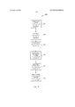
[0039] На фиг. 4 показана примерная блок-схема 400 для возбуждения дисплея с локальным затемнением. На этапе 402 могут генерироваться сигналы возбуждения подсветки (например, источников 104 света). Работающая подсветка на этапе 404 производит первый свет. Первый свет может представлять собой широкополосный свет (например, белый свет), UV спектральные составляющие, синие спектральные составляющие или любую часть спектра. Как показано на этапе 406, первый свет преобразуется во второй свет. Например, преобразующий слой получает первый свет, производит второй свет необходимых цветов (например, красного или зеленого света).[0039] FIG. 4 shows an example block diagram 400 for driving a local dimming display. At 402, backlight drive signals (e.g., light sources 104) may be generated. The working backlight in
[0040] Далее на этапе 408 значения возбуждения для модулятора (например, LCD панели), предпочтительно подпиксельного модулятора для каждого основного цвета, генерируются в зависимости от входных данных изображения. Результаты одного или нескольких имитационных моделирований светового поля могут использоваться для регулирования, изменения или уравновешивания значений возбуждения модулятора, как это отражено на этапе 412. На этапе 410 осуществляется одно или несколько имитационных моделирований светового поля для компенсации. Как описано в данной заявке, имитационные моделирования светового поля в качестве примеров могут решать вопросы, связанные с (i) цветовыми сдвигами в зависимости от функции рассеяния точки подсветки, (ii) разницей между эксплуатационной характеристикой источника света одного или нескольких источников света подсветки и эксплуатационной характеристикой подсветки, (iii) колебанием температуры от производительности, или (iv) их сочетаниями.[0040] Next, at 408, excitation values for a modulator (eg, LCD panel), preferably a sub-pixel modulator for each primary color, are generated depending on the input image data. The results of one or more simulations of the light field can be used to control, change, or balance the excitation values of the modulator, as reflected in
[0041] Следует понимать, что блок-схема 400, описанная в данной заявке, приведена только для наглядности, и что в свете этого специалистам в данной области техники будут предложены различные модификации или изменения. В альтернативных реализациях этапы, упоминаемые в блок-схеме 400, могут осуществляться в другом порядке, по сравнению с тем, что отмечен на фиг. 4, могут включать дополнительные этапы и/или могут полностью пропускать некоторые этапы. Например, этапы 402 и 408 в действительности могут выполняться, по существу, одновременно или в обратном порядке. В качестве другого примера этап 410 может выполняться перед этапом 404. Все такие модификации и изменения предназначены для включения в объем настоящего изобретения.[0041] It should be understood that the
[0042] Варианты осуществления включают устройство, содержащее процессор и выполненное с возможностью осуществления любого из вышеуказанных способов, как описано выше.[0042] Embodiments include an apparatus comprising a processor and configured to implement any of the above methods as described above.
[0043] Варианты осуществления включают машиночитаемый носитель данных, содержащий программные команды, которые при выполнении одним или несколькими процессорами вызывают выполнение любого из вышеуказанных способов, как описано выше.[0043] Embodiments include a computer-readable storage medium comprising program instructions that, when executed by one or more processors, cause any of the above methods to be executed as described above.
[0044] Механизмы реализации - обзор оборудования[0044] Implementation Mechanisms - Hardware Overview
[0045] В соответствии с одним из вариантов осуществления описанные в данной заявке способы реализуются с помощью одного или нескольких вычислительных устройств специального назначения. Вычислительные устройства специального назначения могут быть аппаратно реализованы для выполнения способов, или могут содержать такие цифровые электронные устройства, такие как одна или несколько специализированных интегральных схем (ASIC) или программируемых вентильных матриц (FPGA), которые целенаправленно запрограммированы на выполнение способов, или могут содержать один или несколько аппаратных процессоров общего назначения, запрограммированных на выполнение способов в соответствии с программными командами в аппаратно-программном обеспечении, запоминающем устройстве, других устройствах хранения, или их сочетаниях. Такие вычислительные устройства специального назначения для выполнения способов также могут сочетать пользовательский аппаратно-реализованный алгоритм, ASIC, или FPGA с пользовательским программированием. Вычислительные устройства специального назначения могут представлять собой настольные компьютерные системы, портативные компьютерные системы, переносные устройства, сетевые устройства или любое другое устройство, которое содержит аппаратно-реализованный и/или программно-реализованный алгоритм для реализации способов.[0045] In accordance with one embodiment, the methods described herein are implemented using one or more special purpose computing devices. Special-purpose computing devices may be hardware-implemented to execute methods, or may include such digital electronic devices, such as one or more specialized integrated circuits (ASICs) or programmable gate arrays (FPGAs) that are purposefully programmed to execute methods, or may contain one or several general-purpose hardware processors programmed to execute methods in accordance with software instructions in hardware-software m software, storage device, other storage devices, or combinations thereof. Such special-purpose computing devices for performing methods may also combine a user-defined hardware-implemented algorithm, ASIC, or FPGA with user programming. Special-purpose computing devices can be desktop computer systems, portable computer systems, portable devices, network devices, or any other device that contains a hardware-implemented and / or software-implemented algorithm for implementing the methods.
[0046] Например, на фиг. 5 показана структурная схема, иллюстрирующая компьютерную систему 500, на которой может быть реализован вариант осуществления изобретения. Компьютерная система 500 содержит шину 502 или другой механизм связи для передачи информации и аппаратный процессор 504, соединенный с шиной 502 для обработки информации. Аппаратный процессор 504 может представлять собой, например, микропроцессор общего назначения.[0046] For example, in FIG. 5 is a block diagram illustrating a
[0047] Компьютерная система 500 также содержит оперативное запоминающее устройство 506, такое как запоминающее устройство с произвольным доступом (RAM) или другое динамическое запоминающее устройство, соединенное с шиной 502 для хранения информации и команд, которые будут выполняться процессором 504. Оперативное запоминающее устройство 506 может также использоваться для хранения временных переменных или другой промежуточной информации во время выполнения команд для выполнения процессором 504. Такие команды при хранении в носителе данных, доступном для процессора 504, превращают компьютерную систему 500 в машину специального назначения, которая настроена на выполнение операций, определенных командами.[0047] The
[0048] Компьютерная система 500 дополнительно содержит постоянное запоминающее устройство (ROM) 508 или другое статическое запоминающее устройство, соединенное с шиной 502 для хранения статической информации и команд для процессора 504. Устройство 510 хранения данных, такое как магнитный диск или оптический диск, предусмотрено и соединено с шиной 502 для хранения информации и команд.[0048] The
[0049] Компьютерная система 500 может соединяться через шину 502 с дисплеем 512, таким как жидкокристаллический дисплей (LCD), для отображения информации пользователю компьютера. Устройство 514 ввода, содержащее буквенно-цифровые и другие клавиши, соединено с шиной 502 для передачи информации и выбора команд для процессора 504. Другой тип пользовательского устройства ввода представляет собой устройство 516 управления курсором, такое как мышь, шаровой манипулятор или клавиши управления курсором для передачи информации о направлении и выбора команд для процессора 504 и для управления перемещением курсора на дисплее 512. Это устройство ввода, как правило, имеет две степени свободы по двум осям, первой оси (например, x) и второй оси (например, y), что позволяет устройству указывать положения на плоскости.[0049] The
[0050] Компьютерная система 500 может реализовать способы, описанные в данной заявке с использованием индивидуально разработанного аппаратно-реализованного логического блока, одной или нескольких ASIC или FPGA, аппаратно-программно-реализованного и/или программно-реализованного логического блока, что в сочетании с компьютерной системой приводит или программирует компьютерную систему 500 представлять собой машину специального назначения. Согласно одному варианту осуществления способы в данной заявке выполняют с помощью компьютерной системы 500 в результате выполнения процессором 504 одной или нескольких последовательностей одной или нескольких команд, содержащихся в оперативном запоминающем устройстве 506. Такие команды могут считываться в оперативное запоминающее устройство 506 с другого носителя данных, например, устройства 510 хранения данных. Выполнение последовательностей команд, содержащихся в оперативном запоминающем устройстве 506, влечет выполнение процессором 504 этапов процесса, описанных в данной заявке. В альтернативных вариантах осуществления вместо или в сочетании с программными командами может применяться аппаратно запрограммированная схема.[0050]
[0051] Термин "носители данных" в данном контексте относится к любым устройствам хранения, которые хранят данные и/или команды, которые заставляют машину работать определенным образом. Такие носители данных могут включать энергонезависимые носители данных и/или энергозависимые носители данных. Энергонезависимые носители данных включают, например, оптические или магнитные диски, такие как устройство 510 хранения данных. Энергозависимые носители включают динамическое запоминающее устройство, такое как оперативное запоминающее устройство 506. Распространенные формы носителей данных включают, например, флоппи-диск, гибкий магнитный диск, жесткий магнитный диск, твердотельный накопитель, магнитную ленту или любой другой магнитный носитель данных, CD-ROM, любой другой оптической носитель данных, любую физическую среду с сетками отверстий, RAM, PROM и EPROM, FLASH-EPROM, NVRAM, любую другую микросхему или картридж памяти.[0051] The term "storage media" in this context refers to any storage devices that store data and / or instructions that make the machine work in a certain way. Such storage media may include non-volatile storage media and / or volatile storage media. Non-volatile storage media include, for example, optical or magnetic disks, such as a
[0052] Носитель данных отличается от, но может быть использован в сочетании со средой передачи данных. Среда передачи данных участвует в передаче информации между носителями данных. Например, среда передачи данных включает коаксиальные кабели, медный провод и оптоволоконный кабель, включая проводники, которые содержат шину 502. Среда передачи данных может также принимать форму акустических или световых волн, таких как генерируемые во время радиоволновой и инфракрасной передачи данных.[0052] The storage medium is different from, but can be used in combination with, a data medium. The data transmission medium is involved in the transfer of information between data carriers. For example, a data transmission medium includes coaxial cables, copper wire, and fiber optic cable, including conductors that contain a
[0053] Различные формы носителей могут быть задействованы в доставке одной или нескольких последовательностей одной или нескольких команд в процессор 504 для исполнения. Например, команды изначально могут содержаться на магнитном диске или твердотельном накопителе удаленного компьютера. Удаленный компьютер может загрузить команды в свое динамическое запоминающее устройство и послать команды по телефонной линии с применением модема. Модем по месту нахождения компьютерной системы 500 может принимать данные по телефонной линии и использовать инфракрасный передатчик для преобразования данных в инфракрасный сигнал. Приемник инфракрасного излучения может получать данные, передаваемые в инфракрасном сигнале, а соответствующая схема может размещать данные на шине 502. Шина 502 доставляет данные в оперативное запоминающее устройство 506, из которого процессор 504 извлекает и выполняет команды. Команды, полученные оперативным запоминающим устройством 506, факультативно могут храниться в устройстве 510 хранения данных либо до, либо после исполнения процессором 504.[0053] Various forms of media may be involved in delivering one or more sequences of one or more instructions to
[0054] Компьютерная система 500 также содержит интерфейс 518 связи, соединенный с шиной 502. Интерфейс 518 связи предусматривает соединение для двухсторонней передачи данных с сетевой линией 520 связи, которая подключена к локальной сети 522. Например, интерфейс 518 связи может представлять собой каргу цифровой сети с предоставлением комплексных услуг (ISDN), кабельный модем, спутниковый модем или модем для обеспечения соединения для передачи данных с соответствующим типом телефонной линии. В качестве другого примера интерфейс 518 связи может представлять собой карту локальной вычислительной сети (LAN) для обеспечения передачи данных в совместимую LAN. Также могут быть реализованы беспроводные линии связи. В любой такой реализации интерфейс 518 связи посылает и принимает электрические, электромагнитные или оптические сигналы, которые несут потоки цифровых данных, представляющие различные типы информации.[0054] The
[0055] Сетевая линия 520 связи обычно предусматривает передачу данных через одну или несколько сетей к другим устройствам обработки данных. Например, сетевая линия 520 связи может предусматривать соединение по локальной сети 522 с центральным компьютером 524 или с оборудованием передачи данных, управляемым поставщиком 526 услуг Интернет (ISP). ISP 526 в свою очередь предоставляет услуги передачи данных через всемирную сеть пакетной передачи данных, теперь обычно упоминаемую как "Интернет" 528. И локальная сеть 522, и Интернет 528 используют электрические, электромагнитные или оптические сигналы, которые несут потоки цифровых данных. Сигналы в различных сетях и сигналы в сетевой линии 520 связи и в интерфейсе 518 связи, которые доставляют цифровые данные в и из компьютерной системы 500, являются примерами форм среды передачи данных.[0055] A
[0056] Компьютерная система 500 может отправлять сообщения и получать данные, включая программный код, через сеть(и), сетевую линию 520 связи и интерфейс 518 связи. В примере с Интернетом сервер 530 может передавать требуемый код для прикладной программы через Интернет 528, ISP 526, локальную сеть 522 и интерфейс 518 связи. Полученный код может выполняться процессором 504 в том виде, в котором он принят, и/или храниться в устройстве 510 хранения данных или в другом энергонезависимом устройстве хранения данных для последующего выполнения.[0056] The
[0057] Эквиваленты, дополнения, альтернативы и прочее[0057] Equivalents, additions, alternatives, etc.
[0058] В приведенном выше описании были описаны возможные варианты осуществления настоящего изобретения со ссылкой на различные специфические особенности, которые могут изменяться в зависимости от реализации. Таким образом, единственным и исключительным показателем того, что представляет собой изобретение и предполагается заявителями в качестве изобретения, является формула изобретения, которая вытекает из заявки, в специальной форме, в которой указанная формула изобретения публикуется, включая любую последующую правку. Следовательно, отсутствие ограничения, элемент, свойство, признак, преимущество или особенность, которые явно не изложены в формуле изобретения, в любом случае должны ограничивать объем указанной формулы изобретения. Описание и графический материал соответственно следует рассматривать в пояснительном, а не ограничительном смысле. В свете вышеизложенных идей возможны многочисленные модификации и изменения настоящего изобретения.[0058] In the above description, possible embodiments of the present invention have been described with reference to various specific features that may vary depending on implementation. Thus, the only and exceptional indicator of what constitutes an invention and which is contemplated by the applicants as an invention is the claims that follow from the application, in a special form in which the claims are published, including any subsequent revision. Therefore, the absence of a limitation, element, property, feature, advantage or feature, which are not expressly set forth in the claims, should in any case limit the scope of this claims. The description and graphic material, respectively, should be considered in an explanatory rather than restrictive sense. In light of the above ideas, numerous modifications and variations of the present invention are possible.
[0059] Любые явно указанные в данной заявке определения для терминов, содержащихся в указанной формуле изобретения, регулируют значение тех терминов, которые используются в формуле изобретения. Также следует понимать, что для упрощения слово "например" (напр.) означает "для целей демонстрации" (не исчерпывающей), которое отличается от слов "то есть" (т.е.) или "другими словами".[0059] Any definitions explicitly indicated in this application for the terms contained in the specified claims, govern the meaning of those terms that are used in the claims. It should also be understood that for simplicity, the word “for example” (eg) means “for demonstration purposes” (not exhaustive), which differs from the words “that is” (ie) or “in other words”.
Claims (39)
Applications Claiming Priority (3)
| Application Number | Priority Date | Filing Date | Title |
|---|---|---|---|
| US201361775375P | 2013-03-08 | 2013-03-08 | |
| US61/775,375 | 2013-03-08 | ||
| PCT/US2014/016212 WO2014137565A1 (en) | 2013-03-08 | 2014-02-13 | Techniques for dual modulation display with light conversion |
Related Child Applications (1)
| Application Number | Title | Priority Date | Filing Date |
|---|---|---|---|
| RU2017132197A Division RU2744992C2 (en) | 2013-03-08 | 2014-02-13 | Methods for dual modulation display with light conversion |
Publications (2)
| Publication Number | Publication Date |
|---|---|
| RU2015137943A RU2015137943A (en) | 2017-03-13 |
| RU2633103C2 true RU2633103C2 (en) | 2017-10-11 |
Family
ID=51491767
Family Applications (2)
| Application Number | Title | Priority Date | Filing Date |
|---|---|---|---|
| RU2017132197A RU2744992C2 (en) | 2013-03-08 | 2014-02-13 | Methods for dual modulation display with light conversion |
| RU2015137943A RU2633103C2 (en) | 2013-03-08 | 2014-02-13 | Methods for display with double modulation with light transformation |
Family Applications Before (1)
| Application Number | Title | Priority Date | Filing Date |
|---|---|---|---|
| RU2017132197A RU2744992C2 (en) | 2013-03-08 | 2014-02-13 | Methods for dual modulation display with light conversion |
Country Status (11)
| Country | Link |
|---|---|
| US (3) | US9940881B2 (en) |
| EP (1) | EP2965308B1 (en) |
| JP (2) | JP6081618B2 (en) |
| KR (4) | KR102250809B1 (en) |
| CN (2) | CN105009193B (en) |
| BR (2) | BR122017001987B1 (en) |
| ES (1) | ES2830248T3 (en) |
| IN (1) | IN2015KN02736A (en) |
| PL (1) | PL2965308T3 (en) |
| RU (2) | RU2744992C2 (en) |
| WO (1) | WO2014137565A1 (en) |
Families Citing this family (17)
| Publication number | Priority date | Publication date | Assignee | Title |
|---|---|---|---|---|
| US9564078B2 (en) * | 2010-12-17 | 2017-02-07 | Dolby Laboratories Licensing Corporation | Quantum dots for display panels |
| KR102118309B1 (en) | 2012-09-19 | 2020-06-03 | 돌비 레버러토리즈 라이쎈싱 코오포레이션 | Quantum dot/remote phosphor display system improvements |
| EP2965308B1 (en) | 2013-03-08 | 2020-09-09 | Dolby Laboratories Licensing Corporation | Techniques for dual modulation display with light conversion |
| CN111243533B (en) | 2014-03-26 | 2022-11-25 | 杜比实验室特许公司 | Global light compensation in various displays |
| CN108873477B (en) * | 2014-08-21 | 2021-08-17 | 杜比实验室特许公司 | Method, apparatus and storage medium for driving a local dimming display |
| JP2016133640A (en) * | 2015-01-20 | 2016-07-25 | キヤノン株式会社 | Display device and method of controlling the same |
| US10261330B2 (en) | 2015-08-25 | 2019-04-16 | Christie Digital Systems Usa, Inc. | System for producing an output light beam of a given spectrum |
| KR102121676B1 (en) | 2015-09-21 | 2020-06-10 | 돌비 레버러토리즈 라이쎈싱 코오포레이션 | Techniques for operating a display in perceptual code space |
| ES2880414T3 (en) * | 2015-09-24 | 2021-11-24 | Dolby Laboratories Licensing Corp | Light field simulation techniques for dual modulation |
| US10210820B2 (en) | 2016-02-03 | 2019-02-19 | Canon Kabushiki Kaisha | Image display apparatus and method for controlling same |
| JP6859090B2 (en) * | 2016-02-03 | 2021-04-14 | キヤノン株式会社 | Image display device and its control method |
| US10304396B2 (en) * | 2016-10-28 | 2019-05-28 | Himax Display, Inc. | Image processing method for alleviating tailing phenomenon and related imaging processing circuit and display apparatus |
| US10607551B2 (en) | 2017-03-21 | 2020-03-31 | Dolby Laboratories Licesing Corporation | Temperature-compensated LED-backlit liquid crystal displays |
| US11971616B1 (en) * | 2019-04-11 | 2024-04-30 | PixelDisplay Inc. | Apparatus and method for creating highly-functional meta-materials from luminescing nanoparticles |
| JP7500966B2 (en) | 2019-12-24 | 2024-06-18 | セイコーエプソン株式会社 | CIRCUIT DEVICE, DISPLAY DEVICE, ELECTRONIC INSTRUMENT, MOBILE OBJECT, AND CONTROL METHOD |
| CN111707455B (en) * | 2020-07-03 | 2021-08-13 | 深圳爱克莱特科技股份有限公司 | Smooth dimming method and system for lamp |
| CN114203093B (en) * | 2021-12-23 | 2022-10-11 | 长沙惠科光电有限公司 | Display panel color cast compensation method, display module and electronic equipment |
Citations (5)
| Publication number | Priority date | Publication date | Assignee | Title |
|---|---|---|---|---|
| US20090322800A1 (en) * | 2008-06-25 | 2009-12-31 | Dolby Laboratories Licensing Corporation | Method and apparatus in various embodiments for hdr implementation in display devices |
| US20100214282A1 (en) * | 2009-02-24 | 2010-08-26 | Dolby Laboratories Licensing Corporation | Apparatus for providing light source modulation in dual modulator displays |
| RU2456660C2 (en) * | 2008-03-03 | 2012-07-20 | Шарп Кабусики Кайся | Image forming apparatus having optical sensors |
| US20120300465A1 (en) * | 2011-05-26 | 2012-11-29 | Samsung Electronics Co., Ltd. | Display device |
| US20130050293A1 (en) * | 2011-08-30 | 2013-02-28 | Sharp Laboratories Of America, Inc. | Multi-primary display with active backlight |
Family Cites Families (170)
| Publication number | Priority date | Publication date | Assignee | Title |
|---|---|---|---|---|
| US801871A (en) * | 1904-08-02 | 1905-10-17 | Carl Herminghaus | Dyer's jigger. |
| EP0154953B1 (en) | 1984-03-12 | 1991-01-30 | Matsushita Electric Industrial Co., Ltd. | Optical filter and the method of preparing the same |
| JPH0278393A (en) | 1988-09-14 | 1990-03-19 | Hitachi Ltd | Stereoscopic color picture display device |
| JPH0341890A (en) | 1989-07-07 | 1991-02-22 | Pioneer Electron Corp | Beam index type color display device |
| DE69427860T2 (en) | 1993-02-03 | 2002-04-11 | Nitor, San Jose | METHOD AND DEVICE FOR PROJECTING IMAGES |
| JP3187669B2 (en) | 1994-04-01 | 2001-07-11 | 日本碍子株式会社 | Display element and display device |
| US5737045A (en) | 1995-09-22 | 1998-04-07 | Ois Optical Imaging Systems, Inc. | LCD with notch filter |
| US5754159A (en) | 1995-11-20 | 1998-05-19 | Texas Instruments Incorporated | Integrated liquid crystal display and backlight system for an electronic apparatus |
| KR100286828B1 (en) | 1996-09-18 | 2001-04-16 | 니시무로 타이죠 | Flat panel display device |
| JP3787983B2 (en) | 1997-06-18 | 2006-06-21 | セイコーエプソン株式会社 | Optical switching element, image display device, and projection device |
| US6864626B1 (en) | 1998-06-03 | 2005-03-08 | The Regents Of The University Of California | Electronic displays using optically pumped luminescent semiconductor nanocrystals |
| US20050146258A1 (en) | 1999-06-02 | 2005-07-07 | Shimon Weiss | Electronic displays using optically pumped luminescent semiconductor nanocrystals |
| WO2000017903A2 (en) | 1998-09-22 | 2000-03-30 | Fed Corporation | Inorganic-based color conversion matrix element for organic color display devices and method of fabrication |
| JP2001265296A (en) | 2000-01-14 | 2001-09-28 | Sharp Corp | Transmission type liquid crystal display device and image processing method |
| GB2379317A (en) | 2001-08-30 | 2003-03-05 | Cambridge Display Tech Ltd | Optoelectronic display operating by photoluminescence quenching |
| US7015991B2 (en) | 2001-12-21 | 2006-03-21 | 3M Innovative Properties Company | Color pre-filter for single-panel projection display system |
| JPWO2003058726A1 (en) | 2001-12-28 | 2005-05-19 | サンケン電気株式会社 | Semiconductor light emitting device, light emitting display, method for manufacturing semiconductor light emitting device, and method for manufacturing light emitting display |
| JP2003346530A (en) | 2002-05-23 | 2003-12-05 | Nippon Sheet Glass Co Ltd | Planar light source device and image reading device |
| US7003461B2 (en) | 2002-07-09 | 2006-02-21 | Renesas Technology Corporation | Method and apparatus for an adaptive codebook search in a speech processing system |
| EP1525778A2 (en) | 2002-07-23 | 2005-04-27 | Koninklijke Philips Electronics N.V. | Electroluminescent display, electronic device comprising such a display and method of manufacturing an electroluminescent display |
| WO2004025617A2 (en) * | 2002-09-12 | 2004-03-25 | Koninklijke Philips Electronics N.V. | Transflective liquid crystal display with reduced flicker |
| KR100712334B1 (en) | 2002-09-30 | 2007-05-02 | 엘지전자 주식회사 | How to adjust the brightness level of the liquid crystal display |
| EP1550317A1 (en) | 2002-10-01 | 2005-07-06 | Koninklijke Philips Electronics N.V. | Color display device |
| JP4087681B2 (en) | 2002-10-29 | 2008-05-21 | 株式会社日立製作所 | LIGHTING DEVICE AND DISPLAY DEVICE USING THE SAME |
| ATE392122T1 (en) | 2002-12-26 | 2008-04-15 | Koninkl Philips Electronics Nv | COLOR TEMPERATURE CORRECTION FOR LED WITH PHOSPHORUS-BASED WAVELENGTH CONVERSION |
| JP2004325647A (en) | 2003-04-23 | 2004-11-18 | Sharp Corp | Display element |
| DE602004020345D1 (en) | 2003-06-20 | 2009-05-14 | Sharp Kk | DISPLAY |
| US7126254B2 (en) | 2003-07-22 | 2006-10-24 | Ngk Insulators, Ltd. | Actuator element and device including the actuator element |
| US7052152B2 (en) | 2003-10-03 | 2006-05-30 | Philips Lumileds Lighting Company, Llc | LCD backlight using two-dimensional array LEDs |
| US7354172B2 (en) | 2004-03-15 | 2008-04-08 | Philips Solid-State Lighting Solutions, Inc. | Methods and apparatus for controlled lighting based on a reference gamut |
| JP4139344B2 (en) | 2004-03-15 | 2008-08-27 | シャープ株式会社 | Display device |
| US7768023B2 (en) | 2005-10-14 | 2010-08-03 | The Regents Of The University Of California | Photonic structures for efficient light extraction and conversion in multi-color light emitting devices |
| KR101121131B1 (en) | 2004-07-27 | 2012-03-20 | 돌비 레버러토리즈 라이쎈싱 코오포레이션 | Rapid image rendering on dual-modulator displays |
| US7113670B2 (en) | 2004-09-15 | 2006-09-26 | Research In Motion Limited | Method and device to improve backlight uniformity |
| JP2006114909A (en) | 2004-10-14 | 2006-04-27 | Agilent Technol Inc | Flash module |
| US7481562B2 (en) | 2004-11-18 | 2009-01-27 | Avago Technologies Ecbu Ip (Singapore) Pte. Ltd. | Device and method for providing illuminating light using quantum dots |
| KR100735148B1 (en) | 2004-11-22 | 2007-07-03 | (주)케이디티 | Backlight unit by phosphorescent diffusion sheet |
| TWI263802B (en) | 2004-12-03 | 2006-10-11 | Innolux Display Corp | Color filter |
| KR101460089B1 (en) * | 2004-12-23 | 2014-11-10 | 돌비 레버러토리즈 라이쎈싱 코오포레이션 | Wide color gamut display, and apparatus and method for displaying images at a viewing area |
| JP5084111B2 (en) | 2005-03-31 | 2012-11-28 | 三洋電機株式会社 | Display device and driving method of display device |
| WO2006107720A1 (en) | 2005-04-01 | 2006-10-12 | Spudnik, Inc. | Display systems and devices having screens with optical fluorescent materials |
| US7791561B2 (en) | 2005-04-01 | 2010-09-07 | Prysm, Inc. | Display systems having screens with optical fluorescent materials |
| JP4432818B2 (en) * | 2005-04-01 | 2010-03-17 | セイコーエプソン株式会社 | Image display device, image display method, and image display program |
| US20060221022A1 (en) | 2005-04-01 | 2006-10-05 | Roger Hajjar | Laser vector scanner systems with display screens having optical fluorescent materials |
| JP2006309219A (en) | 2005-04-25 | 2006-11-09 | Samsung Electronics Co Ltd | Self-luminous liquid crystal display device |
| JP2006309238A (en) | 2005-04-27 | 2006-11-09 | Samsung Electronics Co Ltd | Photoluminescence liquid crystal display |
| US8000005B2 (en) | 2006-03-31 | 2011-08-16 | Prysm, Inc. | Multilayered fluorescent screens for scanning beam display systems |
| KR101110071B1 (en) | 2005-04-29 | 2012-02-24 | 삼성전자주식회사 | Photo-Luminescenct Liquid Crystal Display |
| KR101110072B1 (en) | 2005-06-02 | 2012-02-24 | 삼성전자주식회사 | Photo-Luminescenct Liquid Crystal Display |
| US8718437B2 (en) | 2006-03-07 | 2014-05-06 | Qd Vision, Inc. | Compositions, optical component, system including an optical component, devices, and other products |
| US8215815B2 (en) | 2005-06-07 | 2012-07-10 | Oree, Inc. | Illumination apparatus and methods of forming the same |
| US7733017B2 (en) | 2005-07-08 | 2010-06-08 | Peysakh Shapiro | Display apparatus with replaceable electroluminescent element |
| US7513669B2 (en) * | 2005-08-01 | 2009-04-07 | Avago Technologies General Ip (Singapore) Pte. Ltd. | Light source for LCD back-lit displays |
| WO2007015192A2 (en) * | 2005-08-02 | 2007-02-08 | Koninklijke Philips Electronics N.V. | Display device |
| TWI271883B (en) | 2005-08-04 | 2007-01-21 | Jung-Chieh Su | Light-emitting devices with high extraction efficiency |
| CN101243557B (en) | 2005-08-15 | 2010-11-10 | 皇家飞利浦电子股份有限公司 | Light source and method for generating light with variable color and/or brightness |
| CN100517016C (en) | 2005-10-27 | 2009-07-22 | 鸿富锦精密工业(深圳)有限公司 | Light source and backlight module |
| US7420323B2 (en) | 2005-10-31 | 2008-09-02 | Osram Opto Semiconductors Gmbh | Electroluminescent apparatus having a structured luminescence conversion layer |
| US7321193B2 (en) | 2005-10-31 | 2008-01-22 | Osram Opto Semiconductors Gmbh | Device structure for OLED light device having multi element light extraction and luminescence conversion layer |
| US7486304B2 (en) | 2005-12-21 | 2009-02-03 | Nokia Corporation | Display device with dynamic color gamut |
| US7486854B2 (en) | 2006-01-24 | 2009-02-03 | Uni-Pixel Displays, Inc. | Optical microstructures for light extraction and control |
| US7486354B2 (en) | 2006-01-26 | 2009-02-03 | Hannstar Display Corp. | Backlight module of a liquid crystal display, display device, method of improving color gamut of a display device |
| US20080018558A1 (en) | 2006-04-04 | 2008-01-24 | Microvision, Inc. | Electronic display with photoluminescent wavelength conversion |
| KR100783251B1 (en) | 2006-04-10 | 2007-12-06 | 삼성전기주식회사 | Multi-layered White Light Emitting Diode Using Quantum Dots and Manufacturing Method Thereof |
| WO2007124315A2 (en) | 2006-04-19 | 2007-11-01 | 3M Innovative Properties Company | Transflective lc display having narrow band backlight and spectrally notched transflector |
| US20070268240A1 (en) | 2006-05-19 | 2007-11-22 | Lee Sang-Jin | Display device and method of driving the display device |
| US7825891B2 (en) * | 2006-06-02 | 2010-11-02 | Apple Inc. | Dynamic backlight control system |
| US7880381B2 (en) | 2006-07-05 | 2011-02-01 | Avago Technologies General Ip (Singapore) Pte. Ltd. | LED with light absorbing encapsulant and related methodology |
| US20080074583A1 (en) | 2006-07-06 | 2008-03-27 | Intematix Corporation | Photo-luminescence color liquid crystal display |
| US8947619B2 (en) * | 2006-07-06 | 2015-02-03 | Intematix Corporation | Photoluminescence color display comprising quantum dots material and a wavelength selective filter that allows passage of excitation radiation and prevents passage of light generated by photoluminescence materials |
| US7751663B2 (en) | 2006-09-21 | 2010-07-06 | Uni-Pixel Displays, Inc. | Backside reflection optical display |
| KR20090057114A (en) | 2006-09-27 | 2009-06-03 | 가부시끼가이샤 도시바 | Semiconductor light emitting device, backlight and display device comprising the semiconductor light emitting device |
| GB2442505A (en) | 2006-10-04 | 2008-04-09 | Sharp Kk | A display with a primary light source for illuminating a nanophosphor re-emission material |
| JP4851908B2 (en) | 2006-10-10 | 2012-01-11 | 株式会社 日立ディスプレイズ | Liquid crystal display |
| KR101361861B1 (en) | 2006-11-08 | 2014-02-12 | 엘지디스플레이 주식회사 | Organic light emitting diodes and method of manufacturing the same |
| CN101543084A (en) | 2006-11-30 | 2009-09-23 | Nxp股份有限公司 | Device and method for processing color image data |
| JP2008145551A (en) | 2006-12-06 | 2008-06-26 | Sony Corp | Display device |
| CA2708978C (en) | 2006-12-11 | 2016-03-15 | Tir Technology Lp | Luminaire control system and method |
| US7845822B2 (en) | 2006-12-29 | 2010-12-07 | Koninklijke Philips Electronics N.V. | Illumination device including a color selecting panel for recycling unwanted light |
| US20080172197A1 (en) | 2007-01-11 | 2008-07-17 | Motorola, Inc. | Single laser multi-color projection display with quantum dot screen |
| DE102007009530A1 (en) | 2007-02-27 | 2008-08-28 | Osram Opto Semiconductors Gmbh | Organic light-emitting diode for lighting purposes predominantly emitting white light mixed with colors and composite video signal conversation, comprises substrate layer structure, anode, cathode and intermediate arranged functional layer |
| US8941566B2 (en) | 2007-03-08 | 2015-01-27 | 3M Innovative Properties Company | Array of luminescent elements |
| US8018171B1 (en) | 2007-03-12 | 2011-09-13 | Cirrus Logic, Inc. | Multi-function duty cycle modifier |
| US7478922B2 (en) | 2007-03-14 | 2009-01-20 | Renaissance Lighting, Inc. | Set-point validation for color/intensity settings of light fixtures |
| US20100155749A1 (en) | 2007-03-19 | 2010-06-24 | Nanosys, Inc. | Light-emitting diode (led) devices comprising nanocrystals |
| US7687816B2 (en) | 2007-03-20 | 2010-03-30 | International Business Machines Corporation | Light emitting diode |
| US8456492B2 (en) * | 2007-05-18 | 2013-06-04 | Sony Corporation | Display device, driving method and computer program for display device |
| CN201062757Y (en) | 2007-06-05 | 2008-05-21 | 诸建平 | Illuminating device of white light surface light source |
| US11488545B2 (en) * | 2007-06-13 | 2022-11-01 | Interdigital Madison Patent Holdings, Sas | Device for displaying images comprising two modulation stages |
| JP2010533976A (en) | 2007-07-18 | 2010-10-28 | キユーデイー・ビジヨン・インコーポレーテツド | Quantum dot-based light sheet useful for solid-state lighting |
| WO2009014707A2 (en) | 2007-07-23 | 2009-01-29 | Qd Vision, Inc. | Quantum dot light enhancement substrate and lighting device including same |
| US8585273B2 (en) | 2007-07-31 | 2013-11-19 | Rambus Delaware Llc | Illumination assembly including wavelength converting material |
| TWI345671B (en) | 2007-08-10 | 2011-07-21 | Au Optronics Corp | Thin film transistor, pixel structure and liquid crystal display panel |
| US8128249B2 (en) | 2007-08-28 | 2012-03-06 | Qd Vision, Inc. | Apparatus for selectively backlighting a material |
| JP4856249B2 (en) * | 2007-09-27 | 2012-01-18 | シャープ株式会社 | Display device |
| WO2009041594A1 (en) | 2007-09-28 | 2009-04-02 | Dai Nippon Printing Co., Ltd. | Electroluminescence element |
| KR101376755B1 (en) | 2007-10-09 | 2014-03-24 | 삼성디스플레이 주식회사 | Display device |
| KR101415566B1 (en) | 2007-10-29 | 2014-07-04 | 삼성디스플레이 주식회사 | Display device |
| KR20090044292A (en) * | 2007-10-31 | 2009-05-07 | 삼성전자주식회사 | Display device and driving method thereof |
| US7671542B2 (en) | 2007-11-07 | 2010-03-02 | Au Optronics Corporation | Color control of multi-zone LED backlight |
| JP2009283438A (en) | 2007-12-07 | 2009-12-03 | Sony Corp | Lighting device, display device, and manufacturing method of lighting device |
| JP4613947B2 (en) | 2007-12-07 | 2011-01-19 | ソニー株式会社 | Illumination device, color conversion element, and display device |
| WO2009078426A1 (en) | 2007-12-18 | 2009-06-25 | Idec Corporation | Wavelength converter and light emitting device |
| KR101460155B1 (en) | 2008-01-15 | 2014-11-10 | 삼성전자주식회사 | Backlight unit and liquid crystal display having the same |
| US8029139B2 (en) | 2008-01-29 | 2011-10-04 | Eastman Kodak Company | 2D/3D switchable color display apparatus with narrow band emitters |
| US20090194774A1 (en) | 2008-02-04 | 2009-08-06 | Kismart Corporation | Light source module with wavelength converting structure and the method of forming the same |
| US7832885B2 (en) | 2008-02-05 | 2010-11-16 | Kismart Corporation | Patterned wavelength converting structure |
| BRPI0822306A2 (en) | 2008-02-14 | 2015-06-16 | Sharp Kk | Display device |
| TW200938913A (en) | 2008-03-13 | 2009-09-16 | Kismart Corp | A flat panel display capable of multi-sided viewings and its back light module |
| JP2009251129A (en) | 2008-04-02 | 2009-10-29 | Optoelectronic Industry & Technology Development Association | Color filter for liquid crystal display device and liquid crystal display device |
| JP5369486B2 (en) | 2008-04-28 | 2013-12-18 | 豊田合成株式会社 | Light emitting device |
| EP2120448A1 (en) | 2008-05-14 | 2009-11-18 | Thomson Licensing | Method of processing of a compressed image into a gamut mapped image using spatial frequency analysis |
| US9400212B2 (en) | 2008-06-13 | 2016-07-26 | Barco Inc. | Smart pixel addressing |
| US7988311B2 (en) | 2008-06-30 | 2011-08-02 | Bridgelux, Inc. | Light emitting device having a phosphor layer |
| US8459855B2 (en) * | 2008-07-28 | 2013-06-11 | Munisamy Anandan | UV LED based color pixel backlight incorporating quantum dots for increasing color gamut of LCD |
| US8314767B2 (en) | 2008-08-30 | 2012-11-20 | Sharp Laboratories Of America, Inc. | Methods and systems for reducing view-angle-induced color shift |
| EP2164302A1 (en) | 2008-09-12 | 2010-03-17 | Ilford Imaging Switzerland Gmbh | Optical element and method for its production |
| US7858409B2 (en) | 2008-09-18 | 2010-12-28 | Koninklijke Philips Electronics N.V. | White point compensated LEDs for LCD displays |
| US8294848B2 (en) | 2008-10-01 | 2012-10-23 | Samsung Display Co., Ltd. | Liquid crystal display having light diffusion layer |
| JP2010092705A (en) | 2008-10-08 | 2010-04-22 | Sony Corp | Illuminating device and display device using this |
| US8890902B2 (en) | 2008-10-14 | 2014-11-18 | Dolby Laboratories Licensing Corporation | Backlight simulation at reduced resolutions to determine spatial modulation of light for high dynamic range images |
| TWI416454B (en) | 2008-10-31 | 2013-11-21 | Dynascan Technology Corp | A method for compensating the uniformity of a liquid crystal display with a non - uniform backlight and the display |
| GB0821122D0 (en) | 2008-11-19 | 2008-12-24 | Nanoco Technologies Ltd | Semiconductor nanoparticle - based light emitting devices and associated materials and methods |
| US8363100B2 (en) | 2008-11-19 | 2013-01-29 | Honeywell International Inc. | Three dimensional display systems and methods for producing three dimensional images |
| US8272770B2 (en) | 2009-01-02 | 2012-09-25 | Rambus International Ltd. | TIR switched flat panel display |
| JP5367383B2 (en) | 2009-01-14 | 2013-12-11 | 株式会社東芝 | Display device and driving method thereof |
| WO2010085505A1 (en) | 2009-01-21 | 2010-07-29 | Dolby Laboratories Licensing Corporation | Apparatus and methods for color displays |
| KR101562022B1 (en) | 2009-02-02 | 2015-10-21 | 삼성디스플레이 주식회사 | Light emitting diode unit display device having the same and manufacturing mathod of the light emitting diode unit |
| EP2396784A1 (en) * | 2009-02-11 | 2011-12-21 | Thomson Licensing | Signal generation for led/lcd-based high dynamic range displays |
| KR101584663B1 (en) | 2009-02-17 | 2016-01-13 | 삼성전자주식회사 | Polymer dispersed liquid crystal display apparatus using quantum dot |
| KR101631986B1 (en) | 2009-02-18 | 2016-06-21 | 삼성전자주식회사 | Light guide plate and display apparatus employing the same |
| US20100207865A1 (en) | 2009-02-19 | 2010-08-19 | Zoran Corporation | Systems and methods for display device backlight compensation |
| US9524700B2 (en) | 2009-05-14 | 2016-12-20 | Pure Depth Limited | Method and system for displaying images of various formats on a single display |
| US8379039B2 (en) | 2009-06-07 | 2013-02-19 | Apple Inc. | Reformatting content with proper color-region conversion |
| KR20110012246A (en) | 2009-07-30 | 2011-02-09 | 엘지이노텍 주식회사 | Backlight unit |
| US9341887B2 (en) | 2009-09-11 | 2016-05-17 | Dolby Laboratories Licensing Corporation | Displays with a backlight incorporating reflecting layer |
| KR20110041824A (en) | 2009-10-16 | 2011-04-22 | 엘지디스플레이 주식회사 | Display device using quantum dots |
| KR101318444B1 (en) | 2009-11-23 | 2013-10-16 | 엘지디스플레이 주식회사 | Method of compensating pixel data and liquid crystal display |
| KR101563478B1 (en) | 2009-12-22 | 2015-10-26 | 엘지이노텍 주식회사 | Backlight devices including quantum dots |
| DK2539880T3 (en) * | 2010-02-22 | 2015-05-18 | Dolby Lab Licensing Corp | Methods and systems to reduce energy consumption in double modulation displays |
| US20110205251A1 (en) | 2010-02-22 | 2011-08-25 | David Auld | Passive eyewear stereoscopic viewing system with frequency selective emitter |
| TR201001777A2 (en) | 2010-03-09 | 2011-09-21 | Vestel Elektroni̇k Sanayi̇ Ve Ti̇caret Anoni̇m Şi̇rketi̇@ | Backlight unit and making method for liquid crystal display. |
| US8294168B2 (en) | 2010-06-04 | 2012-10-23 | Samsung Electronics Co., Ltd. | Light source module using quantum dots, backlight unit employing the light source module, display apparatus, and illumination apparatus |
| TW201219835A (en) | 2010-07-28 | 2012-05-16 | Unipixel Displays Inc | Two and three-dimensional image display with optical emission frequency control |
| US8436549B2 (en) * | 2010-08-13 | 2013-05-07 | Bridgelux, Inc. | Drive circuit for a color temperature tunable LED light source |
| US20120050632A1 (en) | 2010-08-31 | 2012-03-01 | Chi Lin Technology Co., Ltd. | Display apparatus having quantum dot layer |
| US8736674B2 (en) | 2010-09-23 | 2014-05-27 | Dolby Laboratories Licensing Corporation | Method and system for 3D display calibration with feedback determined by a camera device |
| US8994714B2 (en) | 2010-09-23 | 2015-03-31 | Dolby Laboratories Licensing Corporation | Method and system for display calibration with feedback determined by a camera device |
| EP2638321B1 (en) | 2010-11-10 | 2019-05-08 | Nanosys, Inc. | Quantum dot films, lighting devices, and lighting methods |
| US9564078B2 (en) * | 2010-12-17 | 2017-02-07 | Dolby Laboratories Licensing Corporation | Quantum dots for display panels |
| KR20120078883A (en) | 2011-01-03 | 2012-07-11 | 엘지전자 주식회사 | Display apparatus |
| KR101177480B1 (en) | 2011-02-14 | 2012-08-24 | 엘지전자 주식회사 | Lighting apparatus and display device comprising the same |
| US9183811B2 (en) | 2011-04-01 | 2015-11-10 | Sharp Kabushiki Kaisha | Method of correcting unevenness of display panel and correction system |
| US8982038B2 (en) * | 2011-05-13 | 2015-03-17 | Samsung Display Co., Ltd. | Local dimming display architecture which accommodates irregular backlights |
| KR101793741B1 (en) | 2011-06-23 | 2017-11-03 | 엘지이노텍 주식회사 | Display device |
| TWI442139B (en) * | 2011-07-21 | 2014-06-21 | 友達光電股份有限公司 | Liquid crystal display device |
| KR20130015714A (en) * | 2011-08-04 | 2013-02-14 | 삼성전자주식회사 | Back light unit and method for controlling led |
| WO2013028900A1 (en) | 2011-08-24 | 2013-02-28 | Dolby Laboratories Licensing Corporation | High dynamic range displays having wide color gamut and energy efficiency |
| WO2013043197A1 (en) | 2011-09-23 | 2013-03-28 | Universal Display Corporation | Digitized oled light source |
| JP5902908B2 (en) | 2011-10-19 | 2016-04-13 | スタンレー電気株式会社 | Semiconductor light emitting device and vehicle lamp |
| JP2013161053A (en) | 2012-02-08 | 2013-08-19 | Nikon Corp | Image display device |
| US20130215136A1 (en) | 2012-02-20 | 2013-08-22 | Apple Inc. | Liquid crystal display with large color gamut |
| TWM437586U (en) | 2012-04-10 | 2012-09-11 | Wen-xing Zhao | LED lamp driving device utilizing power carrier wave to control color temperature / colors |
| US20130335677A1 (en) | 2012-06-15 | 2013-12-19 | Apple Inc. | Quantum Dot-Enhanced Display Having Dichroic Filter |
| US9607556B2 (en) | 2012-06-15 | 2017-03-28 | Dolby Laboratories Licensing Corporation | Systems and methods for controlling dual modulation displays |
| US9864232B2 (en) | 2012-08-10 | 2018-01-09 | Dolby Laboratories Licensing Corporation | Light directed modulation displays |
| US8807817B2 (en) | 2012-08-13 | 2014-08-19 | 3M Innovative Properties Company | Colorful diffractive luminaires providing white light illumination |
| KR102118309B1 (en) | 2012-09-19 | 2020-06-03 | 돌비 레버러토리즈 라이쎈싱 코오포레이션 | Quantum dot/remote phosphor display system improvements |
| EP2965308B1 (en) | 2013-03-08 | 2020-09-09 | Dolby Laboratories Licensing Corporation | Techniques for dual modulation display with light conversion |
| CN103544901B (en) | 2013-11-15 | 2016-04-13 | 北京京东方光电科技有限公司 | Display panel and display packing, display device |
-
2014
- 2014-02-13 EP EP14759775.1A patent/EP2965308B1/en active Active
- 2014-02-13 RU RU2017132197A patent/RU2744992C2/en active
- 2014-02-13 KR KR1020207032334A patent/KR102250809B1/en active Active
- 2014-02-13 KR KR1020207014285A patent/KR102178411B1/en active Active
- 2014-02-13 CN CN201480012700.0A patent/CN105009193B/en active Active
- 2014-02-13 JP JP2015561366A patent/JP6081618B2/en active Active
- 2014-02-13 WO PCT/US2014/016212 patent/WO2014137565A1/en not_active Ceased
- 2014-02-13 IN IN2736KON2015 patent/IN2015KN02736A/en unknown
- 2014-02-13 KR KR1020147027340A patent/KR101563143B1/en active Active
- 2014-02-13 CN CN201811525074.1A patent/CN110060640B/en active Active
- 2014-02-13 BR BR122017001987-2A patent/BR122017001987B1/en active IP Right Grant
- 2014-02-13 ES ES14759775T patent/ES2830248T3/en active Active
- 2014-02-13 KR KR1020147027437A patent/KR102115146B1/en active Active
- 2014-02-13 RU RU2015137943A patent/RU2633103C2/en active
- 2014-02-13 PL PL14759775T patent/PL2965308T3/en unknown
- 2014-02-13 US US14/370,115 patent/US9940881B2/en active Active
- 2014-02-13 BR BR112015020571-2A patent/BR112015020571B1/en active IP Right Grant
-
2017
- 2017-01-18 JP JP2017006743A patent/JP6389288B2/en active Active
-
2018
- 2018-01-31 US US15/884,957 patent/US10657906B2/en active Active
-
2020
- 2020-04-30 US US16/863,451 patent/US11074875B2/en active Active
Patent Citations (5)
| Publication number | Priority date | Publication date | Assignee | Title |
|---|---|---|---|---|
| RU2456660C2 (en) * | 2008-03-03 | 2012-07-20 | Шарп Кабусики Кайся | Image forming apparatus having optical sensors |
| US20090322800A1 (en) * | 2008-06-25 | 2009-12-31 | Dolby Laboratories Licensing Corporation | Method and apparatus in various embodiments for hdr implementation in display devices |
| US20100214282A1 (en) * | 2009-02-24 | 2010-08-26 | Dolby Laboratories Licensing Corporation | Apparatus for providing light source modulation in dual modulator displays |
| US20120300465A1 (en) * | 2011-05-26 | 2012-11-29 | Samsung Electronics Co., Ltd. | Display device |
| US20130050293A1 (en) * | 2011-08-30 | 2013-02-28 | Sharp Laboratories Of America, Inc. | Multi-primary display with active backlight |
Also Published As
Similar Documents
| Publication | Publication Date | Title |
|---|---|---|
| RU2633103C2 (en) | Methods for display with double modulation with light transformation | |
| US10534222B2 (en) | Techniques for dual modulation with light conversion | |
| RU2830646C2 (en) | Display system and method of driving display | |
| HK1218343B (en) | Techniques for dual modulation display with light conversion |