RU2622467C2 - Lens antenna, method for manufacturing and using such antennas and antenna system - Google Patents
Lens antenna, method for manufacturing and using such antennas and antenna system Download PDFInfo
- Publication number
- RU2622467C2 RU2622467C2 RU2015115282A RU2015115282A RU2622467C2 RU 2622467 C2 RU2622467 C2 RU 2622467C2 RU 2015115282 A RU2015115282 A RU 2015115282A RU 2015115282 A RU2015115282 A RU 2015115282A RU 2622467 C2 RU2622467 C2 RU 2622467C2
- Authority
- RU
- Russia
- Prior art keywords
- lens
- antenna
- antenna according
- probe
- probes
- Prior art date
Links
Images
Classifications
-
- H—ELECTRICITY
- H01—ELECTRIC ELEMENTS
- H01Q—ANTENNAS, i.e. RADIO AERIALS
- H01Q19/00—Combinations of primary active antenna elements and units with secondary devices, e.g. with quasi-optical devices, for giving the antenna a desired directional characteristic
- H01Q19/06—Combinations of primary active antenna elements and units with secondary devices, e.g. with quasi-optical devices, for giving the antenna a desired directional characteristic using refracting or diffracting devices, e.g. lens
- H01Q19/062—Combinations of primary active antenna elements and units with secondary devices, e.g. with quasi-optical devices, for giving the antenna a desired directional characteristic using refracting or diffracting devices, e.g. lens for focusing
-
- H—ELECTRICITY
- H01—ELECTRIC ELEMENTS
- H01Q—ANTENNAS, i.e. RADIO AERIALS
- H01Q9/00—Electrically-short antennas having dimensions not more than twice the operating wavelength and consisting of conductive active radiating elements
- H01Q9/04—Resonant antennas
- H01Q9/0485—Dielectric resonator antennas
-
- H—ELECTRICITY
- H01—ELECTRIC ELEMENTS
- H01Q—ANTENNAS, i.e. RADIO AERIALS
- H01Q1/00—Details of, or arrangements associated with, antennas
- H01Q1/48—Earthing means; Earth screens; Counterpoises
-
- H—ELECTRICITY
- H01—ELECTRIC ELEMENTS
- H01Q—ANTENNAS, i.e. RADIO AERIALS
- H01Q15/00—Devices for reflection, refraction, diffraction or polarisation of waves radiated from an antenna, e.g. quasi-optical devices
- H01Q15/02—Refracting or diffracting devices, e.g. lens, prism
- H01Q15/08—Refracting or diffracting devices, e.g. lens, prism formed of solid dielectric material
-
- H—ELECTRICITY
- H01—ELECTRIC ELEMENTS
- H01Q—ANTENNAS, i.e. RADIO AERIALS
- H01Q19/00—Combinations of primary active antenna elements and units with secondary devices, e.g. with quasi-optical devices, for giving the antenna a desired directional characteristic
- H01Q19/06—Combinations of primary active antenna elements and units with secondary devices, e.g. with quasi-optical devices, for giving the antenna a desired directional characteristic using refracting or diffracting devices, e.g. lens
- H01Q19/08—Combinations of primary active antenna elements and units with secondary devices, e.g. with quasi-optical devices, for giving the antenna a desired directional characteristic using refracting or diffracting devices, e.g. lens for modifying the radiation pattern of a radiating horn in which it is located
-
- H—ELECTRICITY
- H01—ELECTRIC ELEMENTS
- H01Q—ANTENNAS, i.e. RADIO AERIALS
- H01Q5/00—Arrangements for simultaneous operation of antennas on two or more different wavebands, e.g. dual-band or multi-band arrangements
- H01Q5/30—Arrangements for providing operation on different wavebands
- H01Q5/307—Individual or coupled radiating elements, each element being fed in an unspecified way
- H01Q5/342—Individual or coupled radiating elements, each element being fed in an unspecified way for different propagation modes
- H01Q5/35—Individual or coupled radiating elements, each element being fed in an unspecified way for different propagation modes using two or more simultaneously fed points
-
- H—ELECTRICITY
- H01—ELECTRIC ELEMENTS
- H01Q—ANTENNAS, i.e. RADIO AERIALS
- H01Q5/00—Arrangements for simultaneous operation of antennas on two or more different wavebands, e.g. dual-band or multi-band arrangements
- H01Q5/40—Imbricated or interleaved structures; Combined or electromagnetically coupled arrangements, e.g. comprising two or more non-connected fed radiating elements
- H01Q5/45—Imbricated or interleaved structures; Combined or electromagnetically coupled arrangements, e.g. comprising two or more non-connected fed radiating elements using two or more feeds in association with a common reflecting, diffracting or refracting device
-
- H—ELECTRICITY
- H04—ELECTRIC COMMUNICATION TECHNIQUE
- H04B—TRANSMISSION
- H04B7/00—Radio transmission systems, i.e. using radiation field
- H04B7/02—Diversity systems; Multi-antenna system, i.e. transmission or reception using multiple antennas
- H04B7/12—Frequency diversity
-
- Y—GENERAL TAGGING OF NEW TECHNOLOGICAL DEVELOPMENTS; GENERAL TAGGING OF CROSS-SECTIONAL TECHNOLOGIES SPANNING OVER SEVERAL SECTIONS OF THE IPC; TECHNICAL SUBJECTS COVERED BY FORMER USPC CROSS-REFERENCE ART COLLECTIONS [XRACs] AND DIGESTS
- Y10—TECHNICAL SUBJECTS COVERED BY FORMER USPC
- Y10T—TECHNICAL SUBJECTS COVERED BY FORMER US CLASSIFICATION
- Y10T29/00—Metal working
- Y10T29/49—Method of mechanical manufacture
- Y10T29/49002—Electrical device making
- Y10T29/49016—Antenna or wave energy "plumbing" making
- Y10T29/49018—Antenna or wave energy "plumbing" making with other electrical component
Landscapes
- Physics & Mathematics (AREA)
- Electromagnetism (AREA)
- Engineering & Computer Science (AREA)
- Computer Networks & Wireless Communication (AREA)
- Signal Processing (AREA)
- Aerials With Secondary Devices (AREA)
- Variable-Direction Aerials And Aerial Arrays (AREA)
- Control Of Motors That Do Not Use Commutators (AREA)
- Transceivers (AREA)
- Support Of Aerials (AREA)
Abstract
Description
ВВЕДЕНИЕINTRODUCTION
Изобретение относится к линзовой антенне. Изобретение также относится к антенной системе для передачи и приема электромагнитных сигналов, которая включает по меньшей мере одну антенну согласно изобретению. Изобретение кроме того относится к способу изготовления антенны согласно изобретению. Изобретение также относится к способу для использования в беспроводной связи с применением антенны согласно изобретению. Изобретение помимо этого относится к РЧ-приемопередатчику устройства для беспроводной связи, включающего по меньшей мере одну антенну согласно изобретению. Изобретение кроме того относится к электронному устройству, включающему РЧ-приемопередатчик согласно изобретению.The invention relates to a lens antenna. The invention also relates to an antenna system for transmitting and receiving electromagnetic signals, which includes at least one antenna according to the invention. The invention further relates to a method for manufacturing an antenna according to the invention. The invention also relates to a method for use in wireless communication using an antenna according to the invention. The invention also relates to an RF transceiver of a device for wireless communication, comprising at least one antenna according to the invention. The invention further relates to an electronic device including an RF transceiver according to the invention.
Возрастающий спрос на передачу данных и подключаемость привел к разработке новых способов выполнения существующих и появляющихся требований к связи. Путь, которым проходят данные из источника до назначения, называется каналом связи. Первичные источники помех, которые влияют на системы беспроводной связи, по характеру электромагнитные и могут приводить к нарушению магнитной и радиочастоты или скачкообразному выходу из строя электронных систем, систем связи и передачи информации. Собственные физические, технические и механические параметры конструкций каналов передачи данных (т.е., оптоволоконных или кабельных) часто имеют некоторый уровень иммунитета от источников шума и помех. Помимо этого, проводные медийные средства имеют определенные признаки, которые могут ограничивать влияние шума и помех, которое отрицательно влияет на беспроводные каналы передачи данных. Беспроводные каналы передачи данных имеют свободное распространение в пространстве и подвержены помехам и нарушению сигнала от широкого спектра источников. Это составляет одну из наиболее крупных задач для разработчиков таких систем, поскольку трудно, а в некоторых случаях невозможно изолировать среду передачи от источников электромагнитных и радиочастотных помех. Технологии беспроводной связи используют широкий диапазон электромагнитного спектра, включая высокую частоту, очень высокую частоту, сверхвысокую частоту и оптическую частоту. Влияния шума и помех отличаются в разных сегментах или частотах электромагнитного спектра. Для решения этих проблем необходимо уделить серьезное внимание расчетам параметров каналов беспроводной передачи данных, которые адекватно выполняют требования к связи, и вопросам, относящимся к помехам и нарушению сигнала. Если учитывать потенциальные источники помех во время проектирования таких систем, можно значительно влиять на подключаемость, надежность и скорость канала передачи данных. Повышенная зависимость от беспроводных сетей, сетей передачи данных и сегментов беспроводных сетей вводит дополнительную уязвимость по отношению к эксплуатации и живучести сети. Эти беспроводные системы подвержены помехам, связанным с заторами на полосе частот, и возможности появления источника намеренных помех. Способность передавать направленную энергию на критические беспроводные узлы может привести к временному или постоянному нарушению подключаемости сети и услуг.The increasing demand for data transfer and connectivity has led to the development of new ways to meet existing and emerging communication requirements. The path that the data travels from the source to the destination is called the communication channel. The primary sources of interference that affect wireless communication systems are electromagnetic in nature and can lead to a violation of the magnetic and radio frequencies or an abrupt failure of electronic systems, communication systems and information transfer. Own physical, technical and mechanical parameters of the design of data transmission channels (i.e., fiber or cable) often have some level of immunity from sources of noise and interference. In addition, wired media have certain features that can limit the effects of noise and interference, which adversely affects wireless data channels. Wireless data channels are freely distributed in space and are subject to interference and signal disruption from a wide range of sources. This is one of the largest tasks for developers of such systems, since it is difficult, and in some cases impossible to isolate the transmission medium from sources of electromagnetic and radio frequency interference. Wireless technologies utilize a wide range of electromagnetic spectrum, including high frequency, very high frequency, ultra high frequency and optical frequency. The effects of noise and interference differ in different segments or frequencies of the electromagnetic spectrum. To solve these problems, it is necessary to pay serious attention to the calculation of the parameters of wireless data transmission channels that adequately fulfill the communication requirements, and issues related to interference and signal disruption. If you consider the potential sources of interference during the design of such systems, you can significantly affect the connectivity, reliability and speed of the data channel. Increased reliance on wireless networks, data networks and segments of wireless networks introduces additional vulnerability to the operation and survivability of the network. These wireless systems are prone to interference due to bandwidth congestion and the potential for a source of intentional interference. The ability to transmit directed energy to critical wireless nodes can lead to a temporary or permanent disruption in network connectivity and services.
Помимо этого, учитывая последние достижения в области беспроводной связи, значительно возросла потребность в компактных, низкопрофильных и высокоэффективных антеннах. Наибольшим спросом эти антенны пользуются в системах персональной связи (например, в сотовых телефонах, пейджерах, мобильных системах передачи данных и системах глобального позиционирования) и в других мобильных областях применения (например, в автомобилях и поездах). В зависимости от области применения, существуют различия в требованиях к эксплуатационным характеристикам антенн (например, к усилению, ширине полосы частот, поляризации). Однако компактные и низкопрофильные антенны имеют особенно высокое значение для таких применений как по механическим причинам, так и из-за миниатюризации электронного оборудования в общем. Хорошо известно, что при уменьшении размера антенны КПД стремится к снижению, и ширина полосы частот сужается. Поэтому конфликтующий характер требований к высоким эксплуатационным характеристикам при компактном размере сильно затрудняет разработку этих антенн. Помимо этого, взаимодействие антенны с ее комплексной средой также влияет на ее эксплуатационные характеристики. Эти среды могут включать присутствие тела пользователя или других сложных структур.In addition, given the recent advances in wireless communications, the need for compact, low-profile and high-performance antennas has grown significantly. These antennas are most in demand in personal communication systems (for example, in cell phones, pagers, mobile data transmission systems and global positioning systems) and in other mobile applications (for example, in cars and trains). Depending on the application, there are differences in the performance requirements of the antennas (e.g. gain, bandwidth, polarization). However, compact and low-profile antennas are especially important for such applications, both for mechanical reasons and because of the miniaturization of electronic equipment in general. It is well known that with decreasing antenna size, efficiency tends to decrease, and the bandwidth narrows. Therefore, the conflicting nature of the requirements for high performance with a compact size greatly complicates the development of these antennas. In addition, the interaction of the antenna with its integrated environment also affects its performance. These environments may include the presence of the user's body or other complex structures.
В патентной заявке США №US 2010/0220031 раскрыта широкополосная диэлектрическая антенна, включающая площадку заземления, на которой смонтирована диэлектрическая конструкция, в которой многочисленные фидерные полосы, действующие в качестве зондов, прикреплены к наружной поверхности этой диэлектрической конструкции.U.S. Patent Application No. US 2010/0220031 discloses a broadband dielectric antenna including an earth ground on which a dielectric structure is mounted in which multiple feeder strips acting as probes are attached to the outer surface of this dielectric structure.
В международной патентной заявке WO 2005/093905 раскрыта антенна, включающая первую группу отчасти сферических диэлектрических линз, опирающихся на первую часть проводящей площадки заземления, расположенной так, чтобы отражать сигналы, поступающие с линзы, причем каждая из линз имеет некоторое число соответственных коммутируемо выбираемых фидерных элементов антенны, расположенных по периметру по меньшей мере одного сектора линзы, для подачи сигналов в линзу и/или приема сигналов, распространяемых линзой, и причем каждая линза и связанные с ней фидерные элементы первой группы имеют отличную от других ориентацию и могут эксплуатироваться так, чтобы обеспечивать покрытие в отношении отдельной области. Антенна также включает вторую группу из одной или нескольких сферических или отчасти сферических линз и связанных с ними коммутируемо выбираемых фидерных элементов антенны, ориентированных и эксплуатируемых так, чтобы обеспечивать покрытие области, отличающейся от области покрытия линзами первой группы.International patent application WO 2005/093905 discloses an antenna comprising a first group of partially spherical dielectric lenses supported by a first part of a conductive grounding pad arranged to reflect signals from a lens, each lens having a number of respective switchable feeder elements antennas located along the perimeter of at least one sector of the lens for supplying signals to the lens and / or receiving signals propagated by the lens, and each lens and associated s feeder elements of the first group have a different orientation from the other and can be operated so as to provide coverage for a particular area. The antenna also includes a second group of one or more spherical or partly spherical lenses and associated commutation selectable antenna feeder elements, oriented and operated so as to provide coverage for an area different from the coverage area of the lenses of the first group.
Цель настоящего изобретения заключается в том, чтобы предложить антенну с повышенным КПД, которая может быть выполнена в относительно компактной форме.An object of the present invention is to provide an antenna with increased efficiency, which can be made in a relatively compact form.
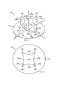
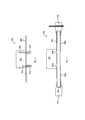
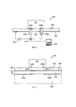
Для достижения этой цели в вариантах осуществления изобретения представлены улучшенные линзовые антенны для широкого класса беспроводных применений (включая сети Wi-Fi). Такая улучшенная линзовая антенна включает: по меньшей мере одну электромагнитную линзу, по меньшей мере одну площадку заземления, соединенную с упомянутой линзой, и по меньшей мере одну зондирующую конструкцию, соединенную с упомянутой линзой, причем упомянутая зондирующая конструкция включает по меньшей мере два зонда, и причем по меньшей мере один зонд окружен линзой, причем взаимная ориентация по меньшей мере двух зондов такова, что они расположены, по меньшей мере частично, вне электромагнитной линии видимости друг друга, и причем электромагнитная линия видимости прерывается, так что зонды не видят друг друга в смысле электромагнетизма. Прежде всего, использование линзовой антенны имеет несколько преимуществ. В линзовой антенне электромагнитная энергия передается от зондирующей конструкции (фидерной системы), следовательно, апертура излучения не загорожена зондирующей конструкцией. Более того, в линзовых антеннах, где электромагнитные волны поступают с одной стороны и выходят с другой стороны, возможна повышенная степень свертывания и кручения без нарушения длины электрического пути, что приводит к высокой эффективности излучения. Кроме того, линзовые антенны могут быть выполнены в относительно компактной форме. Еще одно важное преимущество линзовых антенн заключается в том, что путем выборочного формирования (проектирования) линзы линзовой антенны можно сформировать схему внутреннего (внутри линзы) излучения и схему испускаемого излучения, чтобы противодействовать помехам, о чем будет сказано ниже. Помимо этого, линзовые антенны могут быть легко интегрированы с планарными схемами. Использование нескольких зондов в одной линзовой антенне имеет дополнительное преимущество в том, что передающая и/или принимающая способность линзовой антенны будет улучшена относительно эффективно, что также позволит использовать антенну в качестве многодиапазонной. Если идентичные антенные элементы размещены в антенной решетке или если используются несколько разных антенн, они взаимодействуют друг с другом. Это взаимодействие между элементами из-за их близости друг к другу называется взаимной связью, которая влияет на входной импеданс, а также на схему излучения. Выше сказано, что несколько одинаковых антенных зондов могут быть реализованы или для того, чтобы получить повышенный коэффициент усиления с помощью структур решеток, или чтобы по меньшей мере обеспечить двойную поляризацию с помощью двух других антенных зондов. Кроме того, при применении в мобильных станциях даже несколько разных антенных зондов можно использовать в ограниченном доступном пространстве, чтобы обеспечить многодиапазонную работу. Для этих типов антенн взаимная связь определяется просто как значение помех между двумя антенными зондами, которое желательно должно быть как можно меньшим. Для того, чтобы противодействовать взаимной связи, в линзовой антенне согласно изобретению взаимная ориентация по меньшей мере двух зондов такова, что эти зонды расположены, по меньшей мере частично, вне электромагнитной линии видимости друг друга. Поскольку зонды не видят друг друга, электромагнитные помехи в линзе сведены к минимуму. Расположение зондов вне линии видимости друг друга может быть реализовано, например, путем расположения по меньшей мере одного отражающего элемента между зондами, при этом по меньшей мере один отражающий элемент предпочтительно расположен так, что прямая линия между зондами прервана этим по меньшей мере одним отражающим элементом. Это облегчает расположение зондов вне линии. По меньшей мере один отражающий элемент может быть отдельным отражающим элементом. Этот отражающий элемент может быть окружен линзой, при этом отражающий элемент фактически можно рассматривать как отдельный внутренний рефлектор. Однако применение такого отдельного отражающего элемента обычно будет отрицательно влиять на КПД антенны. Поэтому предпочтительно, чтобы электромагнитное излучение, передаваемое по меньшей мере одним зондом, по меньшей мере частично отражалось по меньшей мере одной окружной стенкой линзы в направлении от по меньшей мере одного другого зонда. В этой связи, окружная стенка линзы предпочтительно по меньшей мере частично имеет вогнутую форму, что облегчает прерывание линии видимости зондов. В некоторых вариантах осуществления окружная стенка может быть, по меньшей мере частично, гофрирована или иначе профилирована, чтобы распространять отражение электромагнитного излучения, передаваемого зондом в направлении от по меньшей мере одного другого зонда. В более конкретных вариантах осуществления окружная стенка может быть и, по меньшей мере частично, гофрированной и, по меньшей мере частично, имеет вогнутую форму чтобы распространять отражение электромагнитного излучения, передаваемого зондом в направлении от по меньшей мере одного другого зонда.To achieve this, embodiments of the invention provide improved lens antennas for a wide class of wireless applications (including Wi-Fi networks). Such an improved lens antenna includes: at least one electromagnetic lens, at least one grounding pad connected to said lens, and at least one probing structure connected to said lens, said probing structure including at least two probes, and moreover, at least one probe is surrounded by a lens, and the mutual orientation of at least two probes is such that they are located at least partially outside the electromagnetic line of sight of each other, and ektromagnitnaya line of sight is interrupted, so that the probe can not see each other in terms of electromagnetism. First of all, using a lens antenna has several advantages. In the lens antenna, electromagnetic energy is transmitted from the probe structure (feeder system), therefore, the radiation aperture is not blocked by the probe structure. Moreover, in lens antennas, where electromagnetic waves enter from one side and exit from the other, an increased degree of coagulation and torsion is possible without violating the length of the electrical path, which leads to high radiation efficiency. In addition, the lens antennas can be made in a relatively compact form. Another important advantage of lens antennas is that by selectively forming (designing) the lens of the lens antenna, it is possible to form a circuit of internal (inside the lens) radiation and a pattern of emitted radiation to counteract the interference, which will be discussed below. In addition, lens antennas can be easily integrated with planar circuits. The use of multiple probes in a single lens antenna has the additional advantage that the transmitting and / or receiving ability of the lens antenna will be improved relatively efficiently, which will also allow the antenna to be used as a multi-band. If identical antenna elements are located in the antenna array or if several different antennas are used, they interact with each other. This interaction between the elements due to their proximity to each other is called mutual coupling, which affects the input impedance, as well as the radiation pattern. It has been said above that several identical antenna probes can be implemented either in order to obtain an increased gain using lattice structures, or at least to provide double polarization using two other antenna probes. In addition, when used in mobile stations, even several different antenna probes can be used in a limited available space to provide multi-band operation. For these types of antennas, mutual coupling is simply defined as the value of the interference between the two antenna probes, which should preferably be as small as possible. In order to counteract the mutual coupling, in the lens antenna according to the invention, the mutual orientation of the at least two probes is such that these probes are located at least partially outside the electromagnetic line of sight of each other. Since the probes do not see each other, electromagnetic interference in the lens is minimized. The arrangement of the probes outside the line of sight of each other can be realized, for example, by positioning at least one reflecting element between the probes, at least one reflecting element is preferably located so that a straight line between the probes is interrupted by this at least one reflecting element. This makes it easier to position probes out of line. At least one reflective element may be a separate reflective element. This reflective element can be surrounded by a lens, while the reflective element can actually be considered as a separate internal reflector. However, the use of such a separate reflective element will usually adversely affect the antenna efficiency. Therefore, it is preferable that the electromagnetic radiation transmitted by at least one probe is at least partially reflected by at least one circumferential wall of the lens in the direction from at least one other probe. In this regard, the circumferential wall of the lens is preferably at least partially concave, which facilitates the interruption of the line of sight of the probes. In some embodiments, the circumferential wall may be at least partially corrugated or otherwise profiled to propagate the reflection of electromagnetic radiation transmitted by the probe from at least one other probe. In more specific embodiments, the circumferential wall may be at least partially corrugated and at least partially concave in order to propagate the reflection of electromagnetic radiation transmitted by the probe from at least one other probe.
Антенна согласно изобретению может быть использована для приема и/или передачи электромагнитного излучения. Функциональность зондирующей конструкции поэтому зависит от желательной функциональности антенны. Таким образом реально, что зондирующая конструкция конфигурирована для приема и/или передачи электромагнитного излучения. Обычно зондирующая конструкция включает по меньшей мере один зонд. Геометрия, включая форму и размеры, зонда обычно полностью зависит от конкретного назначения и применения антенны. Могут быть использованы зонды разных типов. Хорошо известным зондом является зонд с коаксиальным возбуждением, который по меньшей мере частично расположен в линзе, при этом зонд, таким образом, по меньшей мере частично окружен линзой. В этой связи, линза имеет пространство для размещения зонда. Зонд также может быть сформирован волноводом, который не проходит в линзу и просто соединен с базовой плоскостью линзы. В некоторых вариантах осуществления зонд может быть сформирован микрополоской, которая проходит до базовой плоскости линзы. В еще одном альтернативном варианте осуществления зонд сформирован излучателем, который расположен между площадкой заземления и линзой. Применение излучателя обычно будет передавать генерацию фронта сферической волны и, поэтому, распространение по существу однородной плотности мощности в линзе. Следовательно, в линзовой антенне согласно настоящему изобретению можно использовать зонды разных типов.An antenna according to the invention can be used to receive and / or transmit electromagnetic radiation. The functionality of the probe design therefore depends on the desired functionality of the antenna. Thus, it is real that the probing structure is configured to receive and / or transmit electromagnetic radiation. Typically, the probe structure includes at least one probe. The geometry, including the shape and size of the probe, usually completely depends on the specific purpose and application of the antenna. Different types of probes can be used. A well-known probe is a probe with coaxial excitation, which is at least partially located in the lens, while the probe is thus at least partially surrounded by the lens. In this regard, the lens has space to accommodate the probe. The probe can also be formed by a waveguide that does not pass into the lens and is simply connected to the base plane of the lens. In some embodiments, the probe may be formed by a microstrip that extends to the basal plane of the lens. In yet another alternative embodiment, the probe is formed by an emitter that is located between the ground plane and the lens. The use of an emitter will typically transmit the generation of the front of a spherical wave and, therefore, the propagation of a substantially uniform power density in the lens. Therefore, various types of probes can be used in the lens antenna of the present invention.
В том случае, если в линзовой антенне используется один зонд, антенна подойдет для эксплуатации в одной указанной полосе частот. Частотный диапазон упомянутой полосы частот полностью зависит от применения антенны. Сейчас многие системы мобильной связи используют несколько полос частот, таких как полосы GSM 900/1800/1900 (890-960 МГц и 1710-1990 МГц); универсальные системы мобильной связи (UMTS) и полосы расширения UMTS 3G (1900-2200 МГц и 2500-2700 МГц); полосы частот в спектре СВЧ (1-100 ГГц), в частности, полоса Ka (26,5-40 ГГц) и полоса Ku (12-18 ГГц), используемые для спутниковой связи; и полосы Wi-Fi (точность беспроводной связи)/беспроводных локальных сетей (WLAN) (2400-2500 МГц и 5100-5800 МГц). Однако линзовая антенна согласно предпочтительным вариантам осуществления изобретения не ограничена вышеупомянутым перечнем хорошо известных полос частот.In the event that a single probe is used in the lens antenna, the antenna is suitable for operation in one specified frequency band. The frequency range of said frequency band is completely dependent on the use of the antenna. Now many mobile communication systems use several frequency bands, such as the
Обычно, поскольку одна антенна не может работать на всех этих полосах частот мобильной связи, можно использовать несколько разных антенн, покрывающих эти полосы по отдельности. Однако использование многих антенн обычно ограничено из-за объема и стоимостных ограничений. Поэтому очень важны многодиапазонные и широкополосные антенны для совершения многофункциональных операций для мобильной связи. Многодиапазонная антенна в системе мобильной связи может быть определена как антенна, работающая на конкретных полосах частот, но не на промежуточных частотах между полосами. В этой связи предпочтительно, чтобы зондирующая конструкция включала несколько зондов, ведущих к нескольким антенным портам. Работу этих зондов можно переконфигурировать. В последние годы промышленные и научные сообщества пытаются разрабатывать переконфигурируемые антенны. Этот интерес стимулируется потребностью во внешних интерфейсах для будущих систем СВЧ, которые будут поддерживать все возрастающее число функциональностей, таких как радары, связь, пассивное прослушивание или контроль направления и спектра. Более того, персональные устройства для беспроводной связи или связи между движущимися объектами обычно должны поддерживать большое число стандартов (например, UMTS, Bluetooth, Wi-Fi, WiMAX, DSRC). Переконфигурируемая антенна может повторно использовать собственный объем на разных полосах частот, чтобы ее часть или вся конструкция находилась в конкретном режиме эксплуатации. Переконфигурируемость антенны в известных интерфейсных архитектурах может быть достигнута путем изменения состояния подходящих переключающих устройств, чтобы оптимизировать эксплуатационные характеристики устройства для применения в разных сценариях эксплуатации. Для реализации этой концепции предложены несколько подходов. Большинство из этих подходов основаны или на твердотельных, или на электромеханических переключателях. Первые включают переключатели на базе PIN-диодов, варакторов или полевых транзисторов (ПТ), а последние включают простые реле и ряд типов микроэлектромеханической системы (МЭМС). В предложенной концепции многопортовой антенны, имеющей суперформу, подходящие твердотельные схемы настройки, соединенные с входными выводами антенны, используются для динамической регулировки характеристик соответствующих цепей, таких как рабочая частота, и/или излучающих свойств. Переконфигурируемость устройства в техническом отношении достигается путем изменения состояния возбуждения/нагрузки на его входных портах и, за счет этого, распределения тока в конструкции антенны.Typically, since a single antenna cannot operate on all of these mobile frequency bands, several different antennas can be used to cover these bands individually. However, the use of many antennas is usually limited due to volume and cost constraints. Therefore, multiband and broadband antennas are very important for multifunctional operations for mobile communications. A multi-band antenna in a mobile communication system can be defined as an antenna operating on specific frequency bands, but not on intermediate frequencies between the bands. In this regard, it is preferable that the probing structure includes several probes leading to several antenna ports. The operation of these probes can be reconfigured. In recent years, industrial and scientific communities have been trying to develop reconfigurable antennas. This interest is fueled by the need for external interfaces for future microwave systems that will support an increasing number of functionalities, such as radars, communications, passive listening, or direction and spectrum control. Moreover, personal devices for wireless or communication between moving objects usually must support a large number of standards (for example, UMTS, Bluetooth, Wi-Fi, WiMAX, DSRC). A reconfigurable antenna can reuse its own volume in different frequency bands so that part or all of the structure is in a particular operating mode. The reconfigurability of the antenna in known interface architectures can be achieved by changing the state of suitable switching devices in order to optimize the operational characteristics of the device for use in different operating scenarios. To implement this concept, several approaches are proposed. Most of these approaches are based on either solid state or electromechanical switches. The former include switches based on PIN diodes, varactors, or field effect transistors (PTs), and the latter include simple relays and a number of types of microelectromechanical systems (MEMS). In the proposed concept of a multi-port antenna having a superform, suitable solid-state tuning circuits connected to the input terminals of the antenna are used to dynamically adjust the characteristics of the respective circuits, such as the operating frequency, and / or emitting properties. Technical reconfigurability of the device is achieved by changing the state of excitation / load at its input ports and, due to this, the current distribution in the antenna design.
Принятый механизм множественного возбуждения, учитывающий характеристику легкой настройки антенны в широком диапазоне, должен быть оптимизирован таким образом, чтобы минимизировать уровень паразитной электромагнитной связи между портами антенны (зондами), потенциально приводящей к ухудшению эксплуатационных характеристик устройства. В этом контексте необходимо подчеркнуть, что рассматриваемое устройство фактически действует в качестве антенны на тех частотах, где уровень отражения подводимой энергии не может быть совершенным образом компенсирован коэффициентами передачи между разными портами. Процессы природного резонанса, влияющие на характеристики антенны, могут быть активированы или подавлены путем правильной настройки нагрузочных импедансов Zi на входных портах i=0, 1, …, N, где N - число облучателей антенны. При этом особое внимание должно быть уделено КПД излучения η(Zi) устройства, чтобы довести до максимума подвод мощности в радиосигнал, направленный в желательном направлении в пространстве. В этом отношении легко доказать, что мощность, излучаемая антенной, рассматриваемой как сеть с N портов, может быть выражена векторами падающей и отраженной волн, a=a(Zi) и b=b(Zi) соответственно, следующим образом:The adopted multiple excitation mechanism, taking into account the characteristic of easy tuning of the antenna in a wide range, should be optimized in such a way as to minimize the level of spurious electromagnetic coupling between the antenna ports (probes), potentially leading to a deterioration in the operational characteristics of the device. In this context, it must be emphasized that the device in question actually acts as an antenna at those frequencies where the reflection level of the supplied energy cannot be perfectly compensated for by the transmission coefficients between different ports. Natural resonance processes that affect the characteristics of the antenna can be activated or suppressed by properly setting the load impedances Z i at the input ports i = 0, 1, ..., N, where N is the number of antenna feeds. In this case, special attention should be paid to the radiation efficiency η (Z i ) of the device in order to maximize the supply of power to the radio signal directed in the desired direction in space. In this regard, it is easy to prove that the power emitted by the antenna, considered as a network with N ports, can be expressed by the vectors of the incident and reflected waves, a = a (Z i ) and b = b (Z i ), respectively, as follows:

где индекс H означает транспонирование с сопряжением, и:where the index H means transposition with conjugation, and:
![]()
![]()
является т.н. матрицей рассеяния, где ![]()
![]()
![]()
![]()
где ![]()
![]()
![]()
![]()
![]()
![]()
![]()
![]()
![]()
![]()
При рассмотрении нормализованных волновых векторов ![]()
![]()
![]()
![]()

где ![]()
![]()
Поэтому оптимальная работа антенны явно достигается путем минимизации сингулярных значений σn. Таким образом, для надлежащей работы антенны на представляющих интерес полосах частот может быть выбрано оптимальное условие нагрузки Zi (i=0, 1, …, N) входных портов.Therefore, the optimal operation of the antenna is clearly achieved by minimizing the singular values of σ n . Thus, for proper operation of the antenna in the frequency bands of interest, the optimal load condition Z i (i = 0, 1, ..., N) of the input ports can be selected.
В некоторых вариантах осуществления эти антенны также могут быть использованы в антенных решетках, не только планарных, но и в трехмерных, основанных на трехмерных суперформах. Рассматриваемый класс линзовых антенн можно оптимизировать для проектирования недорогих антенных решеток для беспроводного радара следующего поколения, применений в космосе с основными требованиями в смысле согласования импеданса и свойств излучения. В этом контексте предусматривается применение неравномерно размещенных планарных антенных решеток. Правильное формирование диаграммы направленности при уменьшенном числе антенных элементов приведет к снижению массы, стоимости и сложности питающей сети. Повышенное среднее расстояние между элементами приведет к уменьшению уровня паразитной связи антенны. Из-за апериодического интервала, в видимом пространстве отсутствуют реплики главного лепестка антенны, даже при выполнении сканирования диаграммы. В формировании пучка для предлагаемой конфигурации решетки необходимо контролировать и амплитуду, и фазу каждого антенного элемента. Совместный контроль амплитуды и фазы можно использовать для регулировки уровней боковых лепестков и управления нулями лучше, чем этого можно достигнуть только с контролем фазы.In some embodiments, the implementation of these antennas can also be used in antenna arrays, not only planar, but also in three-dimensional, based on three-dimensional superforms. The class of lens antennas under consideration can be optimized for the design of low-cost antenna arrays for the next generation wireless radar, space applications with basic requirements in the sense of matching impedance and radiation properties. In this context, the use of unevenly placed planar antenna arrays is contemplated. Correct beamforming with a reduced number of antenna elements will lead to a decrease in the mass, cost and complexity of the supply network. The increased average distance between the elements will lead to a decrease in the level of spurious coupling of the antenna. Due to the aperiodic interval, there are no replicas of the main lobe of the antenna in the visible space, even when scanning the chart. In the beam formation for the proposed lattice configuration, it is necessary to control both the amplitude and phase of each antenna element. Joint amplitude and phase control can be used to adjust side lobe levels and control zeros better than this can only be achieved with phase control.
Для того, чтобы придать линзовой антенне желательную многодиапазонную функциональность, желательно сделать геометрию по меньшей мере двух зондов взаимно разной. Как уже сказано, геометрия включает форму и размеры зондов. Путем применения разных геометрий разных зондов можно получить разные характеристики излучения, что легко приведет к желательной многодиапазонной функциональности. Предпочтительная длина зонда зависит от материала линзы, в частности от диэлектрической постоянной материала линзы, и желательной частоты или полосы частот. В качестве примера можно сказать, что в случае полимерной линзы, в частности линзы, изготовленной из поливинилхлорида (ПВХ), которая должна работать в полосе частот 5 ГГц для применения в беспроводной локальной сети (WLAN), длина зонда предпочтительно составляет 4-8 мм. В случае конфигурации другого зонда (той же антенны) для работы в полосе частот 2,4 ГГц, длина зонда предпочтительно составляет 10-18 мм. Диаметр по меньшей мере одного зонда предпочтительно составляет 1-3 мм.In order to give the lens antenna the desired multi-range functionality, it is desirable to make the geometry of at least two probes mutually different. As already mentioned, the geometry includes the shape and size of the probes. By using different geometries of different probes, different radiation characteristics can be obtained, which easily leads to the desired multi-range functionality. The preferred probe length depends on the lens material, in particular on the dielectric constant of the lens material, and the desired frequency or frequency band. As an example, we can say that in the case of a polymer lens, in particular a lens made of polyvinyl chloride (PVC), which should operate in the 5 GHz frequency band for use in a wireless local area network (WLAN), the probe length is preferably 4-8 mm. In the case of the configuration of another probe (the same antenna) for operation in the 2.4 GHz frequency band, the probe length is preferably 10-18 mm. The diameter of the at least one probe is preferably 1-3 mm.
Как сказано выше, линзовая антенна согласно изобретению может быть выполнена в относительно компактных размерах по сравнению с известными антеннами. Высота линзы предпочтительно меньше или равна 5 см, что обычно достаточно для надлежащего функционирования линзовой антенны согласно изобретению.As mentioned above, the lens antenna according to the invention can be made in a relatively compact size compared to known antennas. The height of the lens is preferably less than or equal to 5 cm, which is usually sufficient for the proper functioning of the lens antenna according to the invention.
Линза предпочтительно, по меньшей мере частично, изготовлена из диэлектрического материала, более предпочтительно из диэлектрического материала, имеющего диэлектрическую постоянную от 2 до 90. Путем выбора материала, имеющего относительно высокую диэлектрическую постоянную, можно значительно уменьшить размер линзы. Возможно, чтобы линза была, по меньшей мере частично, изготовлена по меньшей мере из одной керамики. Диэлектрические постоянные ![]()
![]()
![]()
![]()
![]()
![]()
![]()
![]()
![]()
![]()
![]()
![]()
![]()
![]()
![]()
![]()
![]()
![]()
![]()
![]()
![]()
![]()
![]()
![]()
![]()
![]()
![]()
![]()
![]()
![]()
![]()
![]()
Однако в некоторых вариантах осуществления, которые часто предпочтительны, линза, по меньшей мере частично, изготовлена из стекла, в частности из стекла Pyrex® (прозрачное боросиликатное стекло с низким коэффициентом теплового расширения, предлагаемое компанией Corning Incorporated), хрусталя, кварца (диоксида кремния), ферроэлектрических диэлектрических материалов, жидких кристаллов, по меньшей мере одного полимера, в частности поливинилхлорида (ПВХ), полистирола (ПС), полиимида (ПИ), биопластика (пластик, получаемый из возобновляемых источников биомассы, таких как растительные жиры и масла, кукурузный крахмал, горохового крахмала или микробиоты) или фторопластиков; и/или оксида металла, в частности оксида титана, оксида алюминия, оксида бария или оксида стронция. В частности, конкретное применение обычно необходимо готовить с финансовой точки зрения и конструкторской точки зрения. Полимеры относительно дешевы и, более того, им легко придать форму, используя известные способы литья, экструзии и/или термоформования, и даже могут быть выполнены в желательной форме на 3D-принтере, что дает значительную степень свободы конструктору. В этом контексте, в некоторых вариантах осуществления можно применить линзу, включающую оболочку, которая изготовлена, по меньшей мере частично, из по меньшей мере одного типа стекла, хрусталя и/или по меньшей мере одного полимера, закрывающего по меньшей мере одно внутреннее пространство, которое, по меньшей мере частично, заполнено текучей средой, предпочтительно воздухом или деминерализованной водой (в качестве диэлектрика). Применение воздуха и воды уменьшит количество других используемых материалов, что далее снизит стоимость линзы и, поэтому, антенны согласно изобретению. Линза может быть диэлектрическим резонатором, что дает диэлектрическую резонаторную антенну (ДРА). Электромагнитное излучение вводят как радиоволны вовнутрь материала резонатора из схемы передатчика, и эти волны движутся туда и обратно между стенками резонатора, формируя стоячие волны. Стенки резонатора частично прозрачны для радиоволн, позволяя их мощности излучаться в пространство. Эти резонирующие линзы, таким образом, не имеют металлических деталей, которые отрицательно повлияли бы на рассеяние энергии в линзе, и, поэтому, имеют меньшие потери и являются более эффективными чем известные металлические антенны.However, in some embodiments, which are often preferred, the lens is at least partially made of glass, in particular Pyrex ® glass (Corning Incorporated transparent borosilicate glass), crystal, quartz (silicon dioxide) ferroelectric dielectric materials, liquid crystals, at least one polymer, in particular polyvinyl chloride (PVC), polystyrene (PS), polyimide (PI), bioplastics (plastic obtained from renewable bi mass, such as vegetable fats and oils, corn starch, pea starch or microbiota) or a fluoroplastic; and / or metal oxide, in particular titanium oxide, alumina, barium oxide or strontium oxide. In particular, a specific application usually needs to be prepared from a financial point of view and a design point of view. Polymers are relatively cheap and, moreover, they are easy to shape using known methods of casting, extrusion and / or thermoforming, and can even be made in the desired form on a 3D printer, which gives a significant degree of freedom to the designer. In this context, in some embodiments, a lens can be used that includes a shell that is made at least partially of at least one type of glass, crystal and / or at least one polymer covering at least one interior space that at least partially filled with a fluid, preferably air or demineralized water (as dielectric). The use of air and water will reduce the amount of other materials used, which will further reduce the cost of the lens and, therefore, the antenna according to the invention. The lens may be a dielectric resonator, which gives a dielectric resonator antenna (DRA). Electromagnetic radiation is introduced as radio waves inside the resonator material from the transmitter circuit, and these waves move back and forth between the cavity walls, forming standing waves. The walls of the resonator are partially transparent to radio waves, allowing their power to be radiated into space. These resonating lenses, therefore, do not have metal parts that would adversely affect the energy dissipation in the lens, and therefore have less loss and are more effective than known metal antennas.
В предпочтительных вариантах осуществления изобретения улучшенная линзовая антенна включает: по меньшей мере одну электромагнитную линзу, по меньшей мере одну площадку заземления, соединенную с упомянутой линзой, и по меньшей мере одну зондирующую конструкцию, соединенную с упомянутой линзой, причем по меньшей мере одна из по меньшей мере одной электромагнитной линзы и по меньшей мере одной площадки заземления имеет по меньшей мере один базовый профиль, который по существу имеет суперформу, и причем этот базовый профиль, имеющий суперформу, определяется полярной функцией:In preferred embodiments of the invention, the improved lens antenna includes: at least one electromagnetic lens, at least one grounding pad connected to said lens, and at least one probing structure connected to said lens, at least one of at least at least one electromagnetic lens and at least one ground plane has at least one base profile, which essentially has a superform, and this basic profile having a super shape, determined by the polar function:

![]()
![]()
и причем:and moreover:
- ρd(ϕ) - кривая, расположенная в XY - плоскости, и- ρ d (ϕ) is a curve located in the XY plane, and
- ϕ∈[0, 2п) - угловая координата.- ϕ∈ [0, 2p) is the angular coordinate.
Несмотря на то, что предлагаемые антенны исключительно просты по конструкции, легко обрабатываются и, таким образом, являются дешевыми, они на удивление значительно превосходят по своим эксплуатационным характеристикам антенны, в настоящее время используемые в беспроводной связи, в смысле ширины рабочей полосы пропускания, максимального коэффициента усиления и стабильности диаграммы направленности. Кроме того, рассматриваемые антенны используют устойчивую технологию и экологически безвредны. В частности, геометрия базового профиля линзы и/или площадки заземления определяется полярным уравнением, известным в научной литературе как суперформула (или формула Гилиса) и ее обобщением до трехмерных пространств. Суперформула подробно объяснена в патенте США №7,620,527 на имя Й. Гилиса, все раскрытие которого включено в настоящий документ путем ссылки. Помимо этого, настоящая заявка также включает, путем ссылки, все раскрытие предварительной заявки США №61/356,836 с названием "Инструментальный ящик, реализованный на компьютере" на имя Йохана Гилиса, поданной 21 июня 2010 г., все содержание которой включено в настоящий документ путем ссылки, как если бы она была приведена здесь полностью. Кроме того, настоящая заявка также включает, путем ссылки, все раскрытие из заявки на патент США №13/165,240 с названием "Инструментальный ящик, реализованный на компьютере" на имя Йохана Гилиса, поданной 22 июня 2011 г., все содержание которой включено в настоящий документ путем ссылки, как если бы она была приведена здесь полностью. В патенте '527 описаны системы и способы, посредством которых образцы (например, такие как изображения, формы волны, такие как звуки, электромагнитные волны или другие сигналы и т.п.) синтезируют, модулируют и/или анализируют, используя новую математическую формулу, запрограммированную в компьютер. Эта формула может быть использована для создания разных форм, форм волны и других представлений. Формула в значительной степени повышает возможности компьютерных операций и обеспечивает большую экономию памяти компьютера и существенное повышение вычислительной мощности.Despite the fact that the proposed antennas are extremely simple in design, easy to process and thus cheap, they are surprisingly significantly superior in performance to the antennas currently used in wireless communications, in terms of bandwidth, maximum ratio gain and stability of the radiation pattern. In addition, the antennas in question use sustainable technology and are environmentally friendly. In particular, the geometry of the base profile of the lens and / or ground plane is determined by the polar equation, known in the scientific literature as the super formula (or Gilis formula) and its generalization to three-dimensional spaces. The super formula is explained in detail in US Pat. No. 7,620,527 to J. Gilis, the entire disclosure of which is incorporated herein by reference. In addition, this application also includes, by reference, the entire disclosure of provisional application US No. 61/356,836 entitled "Toolbox, implemented on a computer" in the name of Johan Ghilis, filed June 21, 2010, the entire contents of which are incorporated herein by links, as if it were given here in full. In addition, this application also includes, by reference, the entire disclosure from US Patent Application No. 13 / 165,240 titled “Computer Toolbox” in the name of Johan Ghilis, filed June 22, 2011, all of which is incorporated herein the document by reference, as if it were given in full here. The '527 patent describes systems and methods by which samples (e.g., such as images, waveforms, such as sounds, electromagnetic waves or other signals, etc.) are synthesized, modulated and / or analyzed using a new mathematical formula, programmed into the computer. This formula can be used to create different shapes, waveforms, and other representations. The formula significantly increases the capabilities of computer operations and provides great savings in computer memory and a significant increase in computing power.
Геометрическая концепция патента '527 подходит для моделирования и для объяснения, почему определенные естественные формы растут так, как это происходит. Как объяснено в патенте '527, автор изобретения установил, что большинство геометрических и обычных форм, включая круги и многоугольники, могут быть описаны как специальные реализации следующей формулы:The geometric concept of the '527 patent is suitable for modeling and for explaining why certain natural forms grow the way they do. As explained in the '527 patent, the inventor found that most geometric and ordinary shapes, including circles and polygons, can be described as special implementations of the following formula:

![]()
![]()
В патенте '527 объяснено, как эта формула и ее представления могут быть использованы, например, в "синтезе" и "анализе" образцов (т.е., включая, например, стандартные образцы изображений и формы волн, таких как электромагнитные (например, электричество, свет и т.д.), звуковые и другие образцы формы волны или сигнала) и т.п.The '527 patent explains how this formula and its representations can be used, for example, in the “synthesis" and "analysis" of samples (i.e., including, for example, standard image samples and waveforms such as electromagnetic (e.g. electricity, light, etc.), sound and other patterns of waveform or signal), etc.
Для того, чтобы синтезировать разные образцы, параметры в этом уравнении могут быть модифицированы так, чтобы можно было синтезировать разные образцы. В частности, параметры в вышеприведенных уравнениях могут быть усреднены. Путем усреднения или модуляции осевых симметрий (m), экспонент (n1-n3) и/или коротких и длинных осей (а, b), в двух- и трехмерном пространстве можно создавать широкую гамму естественных, искусственных и абстрактных форм.In order to synthesize different samples, the parameters in this equation can be modified so that different samples can be synthesized. In particular, the parameters in the above equations can be averaged. By averaging or modulating axial symmetries (m), exponentials (n 1 -n 3 ) and / or short and long axes (a, b), a wide range of natural, artificial and abstract forms can be created in two- and three-dimensional space.
На Фиг. 1 патента '527 приведена схема, показывающая разные компоненты, которые могут быть включены в разные варианты осуществления для синтеза образцов и/или для анализа образцов с помощью оператора суперформулы. Как сказано в патенте '527. согласно первому аспекту, для целей наглядности со ссылкой на упомянутую Фиг. 1, формы или волны могут быть "синтезированы" путем применения следующих базовых этапов: на первом этапе осуществляется выбор параметров (например, или путем ввода значений в компьютер 10, т.е., посредством клавиатуры 20, сенсорного экрана, указателя мыши, устройства распознавания голоса или другого устройства ввода и т.д., или путем обеспечения указания значений компьютером 10), и компьютер 10 используют для синтеза выбранной суперформы, основанной на выбранных параметрах. На втором, необязательном, этапе суперформула может быть использована для адаптации выбранных форм, вычисления оптимизации и т.д. Этот этап может включать использование: графических программ (например, 2D, 3D и т.д.), ПО для САПР, программы для анализа методом конечных элементов, программы для генерации волн или другое ПО. На третьем этапе результат первого или второго этапа используют для преобразования вычисленных на компьютере суперформ в физическую форму, например, посредством: (а) отображения суперформ 31 на мониторе 30, распечатка суперформ 51 на материале 52, таком как бумага, с помощью принтера 50 (2D или 3D); (b) осуществления автоматизированного производства (например, путем управления внешним устройством 60, таким как оборудование, роботы и т.д., на основе результата этапа 3); (с) генерации звука 71 посредством системы громкоговорителей 70 и т.п.; (d) выполнения стереолитографии; (е) выполнения быстрого прототипирования и/или (f) использования полученного результата иным способом, известным из уровня техники, для преобразования таких форм.In FIG. 1 of the '527 patent is a diagram showing various components that may be included in various embodiments for synthesizing samples and / or for analyzing samples using a superformula operator. As stated in the '527 patent. according to a first aspect, for purposes of illustration, with reference to the aforementioned FIG. 1, the shapes or waves can be “synthesized” by applying the following basic steps: at the first stage, the parameters are selected (for example, or by entering values into the
В патенте '527 описаны синтез (такой как, например, создание форм) и анализ (такой как, например, анализ форм). Что касается анализа, в патенте '527 сказано, что: "В общем, хотя и без ограничения, формы или волны могут быть "проанализированы" путем применения следующих базовых этапов (эти этапы имеют сходство с вышеуказанными этапами синтеза, в обратном порядке): на первом этапе образец может быть просканирован или введен в компьютер (например, в цифровой форме). Например, изображение объекта может быть просканировано (2D или 3D), микрофон может принимать звуковые волны, или могут быть введены электрические сигналы (например, волны), могут быть введены данные с машиночитаемого носителя, такого как, например, CD-ROM, дискета, внутренний или внешний флеш-накопитель и т.д., данные могут быть приняты в режиме онлайн, например, по сети Интернет или Интранет и т.д. Могут быть использованы и другие известные способы ввода, такие как, например, использование цифровых или других камер (например, получение одного изображения или непрерывное получение изображений в реальном времени и т.д.), и т.д. На Фиг. 1 показаны примеры, в которых сканер изображений 100 (например, сканер для документов, используемый для сканирования изображений на материале-носителе, таком как бумага или фотографии, или другое сканирующее устройство) и/или рекордер 200 (например, рекордер, который принимает формы волн через микрофон и т.п.) используют вместе с компьютером 10. На втором этапе изображение анализируют, чтобы определить значения параметров и т.д. для суперформулы. На этом этапе анализируемые сигналы также могут быть идентифицированы, категоризированы, сравнены и т.д. В некоторых случаях компьютерного анализа компьютер может иметь библиотеку или каталог (например, в памяти) примитивов (например, категоризирующих набор суперформ по значениям параметров). В таких случаях компьютер можно затем использовать для аппроксимации, идентификации, классификации и т.д. суперформ на основании информации из библиотеки или каталога. Каталог примитивов можно использовать, например, для первой аппроксимации образцов или форм. На третьем, необязательном, этапе анализируемые сигналы могут быть усреднены согласно необходимости (например, могут быть выполнены операции, подобные описанным выше со ссылкой на второй общий этап или этап синтеза). На четвертом этапе может быть получен результат. Такой результат может включать: (а) получение визуального (например, отображаемого или напечатанного) или слышимого (например, звукового) результата; (b) управление работой конкретного устройства (например, если определены конкретные условия); (с) получение указания, относящегося к анализируемому образцу (например, его идентификация или классификация, идентификация предпочтительной или оптимальной конфигурации, выявление дефекта или отклонения от нормы и т.д.); (d) создание другой формы результата, который был бы очевиден специалистам в данной области. При анализе, после оцифровки образца, компьютер продолжает использовать определенный тип представления. Если образец относится к химии, должен быть выбран график XY. Если это замкнутая форма, следует выбрать модифицированный анализ Фурье. Компьютер должен быть адаптирован (например, посредством ПО) на получение оценки правильных параметров для уравнения, чтобы представить оцифрованный образец.The '527 patent describes synthesis (such as, for example, the creation of forms) and analysis (such as, for example, the analysis of forms). As for the analysis, the '527 patent says that: "In general, although without limitation, the shapes or waves can be" analyzed "by applying the following basic steps (these steps are similar to the above synthesis steps, in reverse order): In the first step, the sample can be scanned or entered into a computer (for example, in digital form.) For example, an image of an object can be scanned (2D or 3D), a microphone can receive sound waves, or electrical signals (for example, waves) can be input, data to be entered from a machine-readable medium, such as, for example, a CD-ROM, floppy disk, internal or external flash drive, etc., data can be received online, for example, via the Internet or Intranet, etc. Can be used and other known input methods, such as, for example, the use of digital or other cameras (for example, obtaining a single image or continuously receiving images in real time, etc.), etc. Fig. 1 shows examples in which image scanner 100 (e.g., a document scanner used for scans images on a carrier material, such as paper or photographs, or another scanning device) and / or a recorder 200 (for example, a recorder that takes waveforms through a microphone, etc.) is used with
Вышеуказанная суперформула дает возможность унифицировать описание естественных и абстрактных форм от элементарных частиц до сложных обобщенных кривых Ламе. Улучшенная антенна согласно вариантам осуществления изобретения позволяет увеличить число степеней свободы для конструирования, открывая путь к широкой гамме излучающих структур и датчиков с настраиваемыми электромагнитными характеристиками.The above super formula makes it possible to unify the description of natural and abstract forms from elementary particles to complex generalized Lame curves. The improved antenna according to the embodiments of the invention allows to increase the number of degrees of freedom for construction, opening the way to a wide range of radiating structures and sensors with adjustable electromagnetic characteristics.
В этом контексте предлагаемые линзовые антенны, имеющие суперформу, дают явные преимущества по причинам снижения потерь (по существу, отсутствуют потери в металле), высокого КПД излучения и легкости интеграции с планарными схемами. Кроме того, они дают высокую степень гибкости и универсальности в широком диапазоне частот, позволяя конструктору приспосабливаться к разным требованиям. Численные исследования и измерения, выполненные на экспериментальном прототипе, соответствующем вступающему в силу стандарту WiMedia, подтверждают, что рассматриваемые антенны способны работать в очень широких полосах частот (превышающих 70%) при сохранении стабильных диаграмм направленности и значений коэффициента усиления. На основании достигнутых результатов можно сделать вывод, что предлагаемые антенны могут найти применение в качестве точек доступа для комнатных мультимедийных радиосистем и там, где желательны широкие, гладкие и стабильные по частоте диаграммы направленности, что является особенно важным в появляющихся дешевых применениях радарной, беспроводной и спутниковой технологий.In this context, the proposed lens antennas having a superform give clear advantages for reasons of reducing losses (there are essentially no losses in the metal), high radiation efficiency, and ease of integration with planar circuits. In addition, they offer a high degree of flexibility and versatility over a wide frequency range, allowing the designer to adapt to different requirements. Numerical studies and measurements performed on an experimental prototype that complies with the WiMedia standard that comes into force confirm that the antennas in question are capable of operating in very wide frequency bands (exceeding 70%) while maintaining stable radiation patterns and gain values. Based on the results achieved, it can be concluded that the proposed antennas can be used as access points for indoor multimedia radio systems and where wide, smooth and frequency-stable radiation patterns are desired, which is especially important in emerging low-cost applications of radar, wireless and satellite technology.
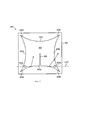
Фактически, каждая линзовая антенна включает линзу и/или площадку заземления, имеющую трехмерную форму. Может быть полезным, чтобы многочисленные профили основания линзы и/или площадки заземления имели по существу суперформу, причем каждый базовый профиль, имеющий суперформу, определяется полярной функцией (суперформулой) по пункту 1 формулы изобретения. Таким образом будет создана трехмерная линза и/или площадка заземления с суперформой, которая обычно будет иметь преимущество в диаграмме распределения мощности и интенсивности линзовой антенны как таковой. В этих трехмерных компонентах с суперформой сначала обычно определяют первый базовый профиль по суперформуле согласно пункту 1 формулы изобретения, и по меньшей мере еще один базовый профиль определяют по суперформуле согласно пункту 1. Оба базовых профиля обычно определяют поперечное сечение конечной суперформы, или, другими словами, первый базовый профиль определяет профиль, а другой базовый профиль определяет путь вращения этого первого базового профиля. Отсюда, трехмерная форма может являться результатом совмещения многих двухмерных форм. Например, квадратный базовый профиль, соединенный с треугольным базовым профилем, дает пирамидальную форму, а каплевидный базовый профиль, соединенный с прямоугольным базовым профилем, дает крыловидную форму. Таким образом можно создавать неопределенное число трехмерных суперформ. Трехмерная форма также может являться результатом объединения наружных граней, причем каждая грань соответствует суперформуле по пункту 1. Например, додекаэдр имеет грани в форме пятиугольника, где каждый пятиугольник соответствует двухмерной суперформуле по пункту 1. То же самое относится, например, к икосаэдру, у которого каждая отдельная грань определена треугольником, соответствующим суперформуле.In fact, each lens antenna includes a lens and / or ground plane having a three-dimensional shape. It may be useful that the multiple profiles of the lens base and / or ground plane have essentially superform, with each basic profile having a superform being determined by the polar function (superformula) of
Параметрическое представление трехмерной формы линзы и/или площадки заземления основано на двух перпендикулярных поперечных сечениях ρ1(ϑ) и ρ2(ϕ):The parametric representation of the three-dimensional shape of the lens and / or ground plane is based on two perpendicular cross sections ρ 1 (ϑ) and ρ 2 (ϕ):

где:Where:
- ρ - определено функцией, представленной в пункте 1 формулы изобретения,- ρ - defined by the function presented in
- 0≤ϑ≤2π и- 0≤ϑ≤2π and
- ½π≤ϕ≤½π.- ½π≤ϕ≤½π.
Записанная как полярная функция, трехмерная форма линзы и/или площадки заземления также может быть определена как:Written as a polar function, the three-dimensional shape of the lens and / or ground plane can also be defined as:

wherein:liver:

и где:and where:
![]()
![]()
- 0≤θ≤2π и- 0≤θ≤2π and
- -½π≤ϕ≤½π.- −1π≤ϕ≤1π.
Вышеприведенная полярная функция может быть переписана в сферических координатах как:The above polar function can be rewritten in spherical coordinates as:

где:Where:
- p и q - параметры симметрии;- p and q are the symmetry parameters;
- γ1, γ2, γ3 - аналогичны параметрам а и b, определенным выше;- γ 1 , γ 2 , γ 3 - are similar to the parameters a and b defined above;
- ν0, ν1, ν2, ν3 - аналоги параметров n0, nx, ny (или n0, n1, n2)- ν 0 , ν 1 , ν 2 , ν 3 - analogues of the parameters n 0 , n x , n y (or n 0 , n 1 , n 2 )
- ![]()
![]()
- (γ1, γ2, γ3, ν0)≥0;- (γ 1 , γ 2 , γ 3 , ν 0 ) ≥0;
- 0≤θ≤π; и- 0≤θ≤π; and
- 0≤ϕ≤2π.- 0≤ϕ≤2π.
Предпочтительно, проектирование линзовой антенны, имеющей суперформу, в частности диэлектрической резонаторной антенны (С-ДРА), осуществляют путем уподобления ее обычной цилиндрической диэлектрической резонаторной антенне. Сначала эффективный радиус основания линзы определяют как:Preferably, the design of a lens antenna having a superform, in particular a dielectric resonator antenna (C-DRA), is carried out by comparing it with a conventional cylindrical dielectric resonator antenna. First, the effective radius of the base of the lens is defined as:

где ρd(ϕ) выражено уравнением Гилиса:where ρ d (ϕ) is expressed by the Ghilis equation:

которое описывает базовый профиль линзы, в частности основания линзы. С другой стороны, высоту линзы (hd) выбирают так, чтобы она была равна приблизительно длине волны в диэлектрическом материале на центральной рабочей частоте антенны (fc), то есть:which describes the basic profile of the lens, in particular the base of the lens. On the other hand, the height of the lens (h d ) is chosen so that it is approximately equal to the wavelength in the dielectric material at the central operating frequency of the antenna (f c ), that is:

гду с0 - скорость света в вакууме, и εr означает относительную диэлектрическую проницаемость материала линзы. Для получения широких рабочих полос частот антенны, размеры поперечного сечения линзы подбирают так, чтобы получить следующее отношение:where 0 is the speed of light in vacuum, and εr means the relative dielectric constant of the lens material. To obtain wide operating frequency bands of the antenna, the dimensions of the cross section of the lens are selected so as to obtain the following ratio:

Местоположение и длину зонда определяют эвристически путем полноволнового анализа.The location and length of the probe is determined heuristically by full-wave analysis.
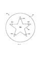
В одном предпочтительном варианте осуществления электромагнитная линза, в частности образованная поверхностью заземления или нижней поверхностью линзы (обычно параллельной площадке заземления), и/или площадка заземления имеет по меньшей мере один базовый профиль по существу суперформы, где m≥4. Это условие параметра дает необычную симметрическую форму линзы, включающую острые края, что приводит к более симметричному пространственному распределению плотности мощности по сравнению с линзой цилиндрической формы, где для одного базового профиля принимается, что m=0. Таким образом, электромагнитное излучение может распространяться в многочисленных сфокусированных направлениях. Присутствие острых углов необязательно снижает КПД предпочтительной антенны. Еще одним предпочтительным граничным условием является то, что а≠b, и, предпочтительно, что по меньшей мере одно значение nx, ny и n0 отклоняется от 2. Эти граничные условия также приводят к линзе необычной формы. Это позволяет располагать зонды на (окружных) острых краях линзы, чтобы минимизировать взаимные помехи зондов. Зонд располагают в отведенном для этого пространстве линзы. Расположение таких пространств предпочтительно такое, что зонды будут расположены вне линии видимости друг друга.In one preferred embodiment, the electromagnetic lens, in particular formed by the ground surface or the bottom surface of the lens (usually parallel to the ground plane), and / or the ground plane has at least one basic profile of a substantially superform, where m≥4. This parameter condition gives an unusual symmetrical shape of the lens, including sharp edges, which leads to a more symmetric spatial distribution of the power density compared to a cylindrical lens, where for one basic profile it is assumed that m = 0. Thus, electromagnetic radiation can propagate in numerous focused directions. The presence of sharp corners does not necessarily reduce the efficiency of the preferred antenna. Another preferred boundary condition is that a ≠ b, and it is preferable that at least one value n x , n y and n 0 deviates from 2. These boundary conditions also lead to an irregularly shaped lens. This allows the probes to be placed on the (circumferential) sharp edges of the lens to minimize mutual interference of the probes. The probe is located in the space provided for this lens. The location of such spaces is preferably such that the probes are located out of line of sight of each other.
Площадка заземления может быть плоской или непланарной, например, изогнутой и/или угловой. В некоторых вариантах осуществления линза и площадка заземления вместе формируют так называемый преобразователь и имеют базовый профиль, который соответствует суперформуле, описанной выше. Также предусматривается, что в некоторых вариантах осуществления площадка заземления и линза имеют одинаковую форму или базовые профили одинаковой формы. Однако в некоторых вариантах осуществления форма площадки заземления может полностью отличаться от формы линзы при условии, что по меньшей мере один базовый профиль по меньшей мере одной из площадки заземления и линзы соответствует суперформуле, сформулированной в пункте 1 формулы изобретения.The ground plane may be flat or non-planar, for example curved and / or angled. In some embodiments, the lens and ground plane together form a so-called transducer and have a base profile that corresponds to the super formula described above. It is also contemplated that in some embodiments, the ground plane and the lens have the same shape or base profiles of the same shape. However, in some embodiments, the shape of the ground plane may be completely different from the shape of the lens, provided that at least one basic profile of at least one of the ground plane and the lens corresponds to the superformula set forth in
Предпочтительно, базовым профилем, имеющим по существу суперформу, является базовый профиль линзы, который проходит в направлении, по существу параллельном плоскости, определяемой площадкой заземления. Обычно это дает ось симметрии, ориентированную перпендикулярно к (центральной) плоскости, определяемой площадкой заземления, что способствует пространственному распределению плотности мощности. Этот вариант осуществления позволяет применять линзу, имеющую (необычную) форму многогранника, такого как призма, где n-стороннее многоугольное основание многогранника направлено на площадку заземления и в конечном счете установлено на ней.Preferably, the base profile having substantially superform is the base profile of the lens, which extends in a direction substantially parallel to the plane defined by the ground plane. Usually this gives an axis of symmetry oriented perpendicular to the (central) plane defined by the ground plane, which contributes to the spatial distribution of power density. This embodiment allows the use of a lens having an (unusual) shape of a polyhedron, such as a prism, where the n-sided polygonal base of the polyhedron is directed to the ground plane and ultimately mounted on it.
В одном предпочтительном варианте осуществления, поверхность площадки заземления, направленная к линзе, по меньшей мере частично отражающая. Площадка заземления может быть плоской или изогнутой (в форме чаши) и включает электропроводящую поверхность, чтобы отражать электромагнитные радиоволны от других антенных элементов. Эта плоскость необязательно должна быть соединена с заземлением. Обычно, чтобы функционировать как площадка заземления, проводящая поверхность должна быть по меньшей мере четвертьволновой (λ/4) от радиоволн. Для более высокой частоты антенны, в диапазоне ОВЧ или УВЧ, площадка заземления может быть образована, например, металлическим диском или сеткой. На верхних ОВЧ и УВЧ частотах металлическая оболочка автомобиля или летательного аппарата может служить в качестве площадки заземления для штыревой антенны, выступающей с нее. Площадка заземления необязательно должна быть сплошной. В площадке заземления антенны "плоскость" состоит из нескольких проводов длиной λ/4, исходящих из основания четвертьволновой штыревой антенны. Радиоволны от линзы (или от другой антенны), которые отражаются от площадки заземления, кажется исходящими от зеркального изображения антенны, расположенного на другой стороне площадки заземления. В несимметричном вибраторе диаграмма направленности антенны плюс виртуального "изображения антенны" делает его похожим на двухэлементную дипольную антенну с центральным питанием. Поэтому несимметричный вибратор, установленный на идеальную площадку заземления, имеет диаграмму направленности, идентичную дипольной антенне. Линия питания от передатчика или приемника подсоединена между нижним концом несимметричного вибраторного элемента и площадкой заземления. Площадка заземления предпочтительно имеет хорошую проводимость; любое сопротивление площадки заземления является последовательным с антенной и служит для рассеяния мощности от передатчика. Площадка заземления может быть объединена с печатной платой (ПП). Это позволяет облегчить схемное решение, позволяя разработчику заземлить любой компонент без необходимости в дополнительных медных дорожках; медный провод компонента, который нужно заземлить, проводят непосредственно через отверстие в плате к площадке заземления на другом слое. Большая площадь меди также проводит большие обратные токи от многих компонентов без значительного падения напряжения, обеспечивая при этом что заземляющее соединение всех компонентов в то же время является опорным потенциалом. Однако для этой специфической цели основная причина использования больших площадок заземления заключается в том, чтобы снизить электрический шум и помехи, наводимые одной частью схемы на другую через заземление (контуры заземления), и перекрестные помехи между соседними дорожками схемы.In one preferred embodiment, the surface of the ground plane toward the lens is at least partially reflective. The grounding pad can be flat or curved (in the shape of a bowl) and includes an electrically conductive surface to reflect electromagnetic radio waves from other antenna elements. This plane does not have to be connected to ground. Typically, in order to function as a ground plane, the conductive surface must be at least a quarter wave (λ / 4) from the radio waves. For a higher frequency of the antenna, in the VHF or UHF range, the ground plane can be formed, for example, by a metal disk or grid. At higher VHF and UHF frequencies, the metal sheath of a car or aircraft can serve as a grounding pad for a whip antenna protruding from it. The grounding pad does not have to be solid. In the ground plane of the antenna, the “plane” consists of several wires with a length of λ / 4, coming from the base of the quarter-wave whip antenna. Radio waves from the lens (or from another antenna) that are reflected from the ground plane appear to be coming from a mirror image of the antenna located on the other side of the ground plane. In an asymmetric vibrator, the antenna pattern plus the virtual “antenna image” makes it look like a two-element dipole antenna with central power supply. Therefore, an asymmetric vibrator mounted on an ideal grounding pad has a radiation pattern identical to a dipole antenna. A power line from a transmitter or receiver is connected between the lower end of the asymmetric vibrator element and the ground plane. The ground plane preferably has good conductivity; any resistance of the grounding pad is consistent with the antenna and serves to dissipate power from the transmitter. The grounding pad can be combined with a printed circuit board (PCB). This makes it easier to circuitry, allowing the developer to ground any component without the need for additional copper tracks; the copper wire of the component to be grounded is drawn directly through the hole in the board to the grounding pad on another layer. The large copper area also conducts large reverse currents from many components without a significant voltage drop, while ensuring that the ground connection of all components is at the same time a reference potential. However, for this specific purpose, the main reason for using large grounding pads is to reduce electrical noise and interference from one part of the circuit to another through grounding (ground loops) and crosstalk between adjacent circuit tracks.
Когда цифровые схемы переключают состояние, большие импульсы тока проходят из интегральных схем через цепь заземления. Если провода питания и заземления имеют значительное сопротивление, падение напряжения на них может создавать импульсы напряжения шума в проводах заземления, которые подаются на другие части схемы. Большая емкость площадки заземления позволяет ей поглощать импульсы тока без большого изменения в напряжении. Помимо этого, площадка заземления под дорожками печатной схемы может снижать перекрестные помехи между соседними дорожками. Когда две дорожки идут параллельно, электрический сигнал в одной может наводиться в другую посредством электромагнитной индукции линиями магнитного поля между которыми образуется связь; это называется перекрестными помехами. Когда слой площадки заземления расположен снизу, он формирует линию передачи (полосковую линию) с дорожкой. Обратные токи противоположного направления проходят через площадку заземления непосредственно под дорожкой. Это ограничивает электромагнитные поля областью между дорожкой и площадкой заземления, снижая перекрестные помехи.When digital circuits switch state, large current pulses pass from the integrated circuits through the ground circuit. If the power and ground wires have significant resistance, the voltage drop across them can create noise voltage pulses in the ground wires, which are supplied to other parts of the circuit. The large capacity of the grounding pad allows it to absorb current pulses without a large change in voltage. In addition, the grounding pad under the tracks of the printed circuit can reduce crosstalk between adjacent tracks. When two tracks go parallel, an electric signal in one can be induced into the other by means of electromagnetic induction by magnetic field lines between which a connection is formed; this is called crosstalk. When the ground plane layer is located below, it forms a transmission line (strip line) with the track. Reverse currents in the opposite direction pass through the ground plane directly below the track. This limits the electromagnetic fields to the area between the track and the ground, reducing crosstalk.
В линзовой антенне модель направленности является результатом разницы между фазовой скоростью распространения электромагнитной волны в воздухе и таковой в материале линзы (n≠1). Форма линзы зависит от показателя преломления n (отношение фазовой скорости распространения радиоволны в вакууме и таковой в линзе). Замедляющей линзовой антенной, как в оптике, является та, для которой n>1. Линза этих типов антенн предпочтительно изготовлена из высококачественных гомогенных диэлектриков с низкими потерями, таких как полимеры.In a lens antenna, the directivity model is the result of the difference between the phase velocity of the electromagnetic wave in air and that of the lens material (n ≠ 1). The shape of the lens depends on the refractive index n (the ratio of the phase velocity of propagation of the radio wave in vacuum and that in the lens). A retarding lens antenna, as in optics, is one for which n> 1. The lens of these types of antennas is preferably made of high quality, low loss homogeneous dielectrics, such as polymers.
Зондирующая конструкция предпочтительно включает по меньшей мере один первый зонд, конфигурированный для связи с первой полосе частот, и по меньшей мере один второй зонд, конфигурированный для связи во второй полосе частот, что позволяет реализовать антенну в системе с многими входами-выходами (MIMO). Технология MIMO разработана недавно как новая технология достижения очень высокой эффективности полосы частот и более высоких скоростей передачи данных в современной беспроводной связи. В технологии MIMO несколько антенн размещены на входной и выходной стороне системы связи для улучшения возможностей канала. Многомерные статистические характеристики канала с замираниями MIMO и расчетные параметры антенн, которые снимают на стороне передатчика и приемника, отвечают за увеличение скоростей передачи данных. Технология MIMO является новейшей парадигмой, в которой несколько антенн используют как в передатчике, так и в приемнике, чтобы улучшить эксплуатационные характеристики связи. Это одна из нескольких форм технологии "умной" антенны. Технология MIMO привлекла внимание в области беспроводной связи, поскольку она дает значительное увеличение пропускной способности канала передачи данных, емкости канала и диапазона связи без дополнительной ширины полосы или увеличения передаваемой мощности. Из-за этих свойств MIMO является важной частью стандартов современной беспроводной связи, таких как IEEE802.11n (Wi-Fi), 4G, 3GPP LTE, WiMAX (Wireless interoperability for microwave access), HSPA (высокоскоростная пакетная передача данных) и т.д. Главная цель систем MIMO заключается в том, что антенны в антенной решетке должны обеспечивать многообразный прием при уменьшенном интервале. Когда антенны расположены близко друг к другу, электромагнитные волны разных антенн мешают друг другу, что приводит к потере сигнала. В системах MIMO крупной проблемой для разработчиков является взаимное влияние, которое возникает в основном из-за электромагнитных взаимодействий между антеннами в решетке. Эта проблема в основном имеет место из-за небольшого интервала между антеннами в решетке. Параллельные доводы применимы к линзовой антенне согласно предпочтительным вариантам осуществления изобретения. Следовательно, полезно поддерживать достаточное расстояние между соседними зондами, чтобы противодействовать взаимному влиянию, в частности, если зондирующая конструкция включает несколько первых зондов и несколько вторых зондов. Это минимальное расстояние зависит от длины волны электромагнитного излучения, материала линзы и геометрии зондов.The probe structure preferably includes at least one first probe configured to communicate with the first frequency band, and at least one second probe configured to communicate in the second frequency band, which makes it possible to realize the antenna in a multi-input-output (MIMO) system. MIMO technology was recently developed as a new technology for achieving very high bandwidth efficiency and higher data rates in modern wireless communications. In MIMO technology, several antennas are located on the input and output sides of the communication system to improve channel capabilities. The multidimensional statistical characteristics of the channel with MIMO fading and the design parameters of the antennas, which are recorded on the side of the transmitter and receiver, are responsible for increasing the data transfer rates. MIMO technology is the latest paradigm in which several antennas are used both in the transmitter and in the receiver to improve communication performance. This is one of several forms of smart antenna technology. MIMO technology has attracted attention in the field of wireless communications, as it provides a significant increase in data throughput, channel capacity and communication range without additional bandwidth or increased transmit power. Because of these properties, MIMO is an important part of modern wireless standards such as IEEE802.11n (Wi-Fi), 4G, 3GPP LTE, WiMAX (Wireless interoperability for microwave access), HSPA (high-speed packet data), etc. . The main goal of MIMO systems is that the antennas in the antenna array must provide diverse reception with a reduced interval. When the antennas are located close to each other, the electromagnetic waves of different antennas interfere with each other, which leads to signal loss. In MIMO systems, a major problem for developers is the mutual influence, which occurs mainly due to electromagnetic interactions between the antennas in the array. This problem mainly occurs due to the small spacing between the antennas in the array. Parallel arguments apply to a lens antenna according to preferred embodiments of the invention. Therefore, it is useful to maintain a sufficient distance between adjacent probes to counteract the mutual influence, in particular if the probing structure includes several first probes and several second probes. This minimum distance depends on the wavelength of electromagnetic radiation, the lens material and the geometry of the probes.
В предпочтительных вариантах осуществления антенна включает по меньшей мере один процессор, чтобы автоматически переключать зондирующую конструкцию между режимом передачи излучения и режимом приема излучения для двухсторонней связи зондирующей конструкции. Более конкретно, процессор предпочтительно конфигурирован для автоматического переключения между первой полосой частот и второй полой частот для двухсторонней связи в каждой полосе частот.In preferred embodiments, the antenna includes at least one processor to automatically switch the probe structure between the radiation transmission mode and the radiation reception mode for two-way communication of the probe structure. More specifically, the processor is preferably configured to automatically switch between the first frequency band and the second frequency field for two-way communication in each frequency band.
На высоких частотах излучающие свойства линзовых антенн, имеющих суперформу, могут быть исследованы специальным асимптотическим методом, основанным на оптической лучевой аппроксимации. В частности, геометрическую оптику адаптируют для анализа распространения электромагнитного поля в области линзы. При этом учитывают вклад многочисленных внутренних отражений, этим повышая точность моделирования, особенно когда в расчетах используются диэлектрические материалы с относительно большой диэлектрической проницаемостью, поскольку в этом случае обычной гипотезой, что содержанием энергии, релевантным для отраженных лучей высокого порядка, можно пренебречь, не применима. В заключение, в силу принципа эквивалентности, электромагнитное поле снаружи линзы можно оценить по излучению в свободном пространстве эквивалентных распределений электрических и магнитных токов на поверхности раздела с областью воздуха. В разработанной методологии расчетов эти токи определяются путем применения локальных коэффициентов френелевской передачи на поверхности линзы в поле в приближении геометрической оптики в соответствии с методом физической оптики. В этом контексте, применение формулы Гилиса транслируется в возможность автоматического изменения формы профиля линзы, так что любая процедура автоматизированной оптимизации, такая как генетические алгоритмы, нейронные сети, метод роя частиц и муравьиный алгоритм, может быть применена для определения геометрических параметров, дающих оптимальные эксплуатационные характеристики антенны.At high frequencies, the radiating properties of lens antennas having a superform can be studied by a special asymptotic method based on optical beam approximation. In particular, geometrical optics are adapted to analyze the propagation of an electromagnetic field in the lens area. At the same time, the contribution of numerous internal reflections is taken into account, thereby increasing the modeling accuracy, especially when dielectric materials with a relatively high dielectric constant are used in the calculations, since in this case the usual hypothesis that the energy content relevant for high-order reflected rays can be neglected is not applicable. In conclusion, by virtue of the principle of equivalence, the electromagnetic field outside the lens can be estimated from the radiation in free space of the equivalent distributions of electric and magnetic currents at the interface with the air region. In the developed calculation methodology, these currents are determined by applying the local Fresnel transmission coefficients on the surface of the lens in the field in the approximation of geometric optics in accordance with the method of physical optics. In this context, the application of the Ghilis formula translates into the ability to automatically change the shape of the lens profile, so that any automated optimization procedure, such as genetic algorithms, neural networks, particle swarm method and ant algorithm, can be applied to determine geometric parameters giving optimal performance antennas.
Распределение электрического поля, передаваемое снаружи области линзы, можно удобно оценить как:The distribution of the electric field transmitted outside the lens area can be conveniently estimated as:
![]()
![]()
при:at:

обозначающем вклад электрического поля, относящийся к процессу внутреннего отражения порядка т. В(7) ![]()
![]()
![]()
![]()
![]()
![]()
![]()
![]()
![]()
![]()
![]()
![]()
![]()
![]()
![]()
![]()


Поле падающего излучения ![]()
![]()
![]()
![]()
![]()
![]()
где d обозначает евклидово расстояние между точкой наблюдения Р и точкой Pm, в которой происходит отражение. Отраженное поле ![]()
![]()

где параллельные и ортогональные компоненты в отношении плоскости падения, ![]()
![]()
![]()
![]()
![]()
![]()
![]()
![]()
![]()
![]()
![]()
![]()
После оценки поля в приближении геометрической оптики эквивалентные плотности электрического ![]()
![]()
![]()
![]()

где ![]()
![]()
Предпочтительные варианты осуществления изобретения также относятся к антенной системе для передачи и приема электромагнитных сигналов, включающей по меньшей мере одну антенну согласно изобретению. Антенная система включает несколько антенн, конфигурированных по принципу MIMO, который описан выше, причем каждая антенна включает несколько зондов. Система предпочтительно также включает по меньшей мере две многодиапазонные антенны и по меньшей мере один процессор для подключения по меньшей мере одной из полос частот, этим обеспечивая разнообразие приема и передачи сигналов в этой полосе. Предпочтительно, процессор конфигурирован для управления средством переключения, которым является переключатель SPDT (однопортовый двухпозиционный) или DPDT (двухпортовый двухпозиционный). Предпочтительно, система также включает по меньшей мере одно интерфейсное средство для программирования по меньшей мере одного процессора и. поэтому, для программирования (конфигурирования) антенны как таковой.Preferred embodiments of the invention also relate to an antenna system for transmitting and receiving electromagnetic signals, comprising at least one antenna according to the invention. The antenna system includes several antennas configured according to the MIMO principle, which is described above, with each antenna including several probes. The system preferably also includes at least two multi-band antennas and at least one processor for connecting at least one of the frequency bands, thereby providing a variety of reception and transmission of signals in this band. Preferably, the processor is configured to control the switching means, which is a switch SPDT (single-port on-off) or DPDT (two-port on-off). Preferably, the system also includes at least one interface means for programming at least one processor and. therefore, for programming (configuring) the antenna as such.
Согласно некоторым вариантам осуществления, изобретение также относится к способу изготовления антенны согласно изобретению, включающему этап сборки площадки заземления, линзы и зондирующей конструкции, причем упомянутая зондирующая конструкция включает несколько зондов, при этом взаимная ориентация по меньшей мере двух зондов такая, что эти зонды расположены, по меньшей мере частично, вне электромагнитной линии видимости друг друга. Согласно некоторым вариантам осуществления, преимущества использования многозондовой линзовой антенны, у которой по меньшей мере два зонда расположены вне линии видимости друг друга, уже были описаны выше в полном объеме. Предпочтительно, по меньшей мере одна площадка заземления и/или по меньшей мере одна линза выполнена так, что площадка заземления и/или линза имеет по меньшей мере один базовый профиль, который имеет по существу суперформу, причем упомянутая суперформа определяется полярной функцией (суперформулой):According to some embodiments, the invention also relates to a method for manufacturing an antenna according to the invention, comprising the step of assembling a ground plane, a lens and a probe structure, said probe structure comprising several probes, wherein at least two probes are mutually oriented such that these probes are located, at least partially, outside each other's electromagnetic line of sight. According to some embodiments, the advantages of using a multi-probe lens antenna in which at least two probes are located out of line of sight of each other have already been fully described above. Preferably, at least one grounding pad and / or at least one lens is configured such that the grounding pad and / or lens has at least one base profile that has substantially superform, said superform being determined by a polar function (superformula):

![]()
![]()
где:Where:
- ρd(ϕ) - кривая, расположенная в плоскости XY; и- ρ d (ϕ) is a curve located in the XY plane; and
- ϕ∈[0, 2п) - угловая координата.- ϕ∈ [0, 2p) is the angular coordinate.
Во время сборки предпочтительно несколько зондов соединяют с площадкой заземления и/или линзой. По меньшей мере один зонд предпочтительно конфигурирован для связи в первой полосе частот, и по меньшей мере один другой зонд конфигурирован для связи во второй полосе частот. Более предпочтительно, разные зонды ориентированы так, что во время эксплуатации будут возбуждаться разные сектора линзы. Предпочтительно, если зонды расположены вне линии видимости, чтобы противодействовать взаимному влиянию.During assembly, preferably several probes are connected to the ground plane and / or lens. At least one probe is preferably configured for communication in a first frequency band, and at least one other probe is configured for communication in a second frequency band. More preferably, the different probes are oriented so that different sectors of the lens are excited during operation. Preferably, if the probes are located out of line of sight to counteract the mutual influence.
Согласно некоторым вариантам осуществления, изобретение кроме того относится к способу для использования в беспроводной связи путем использования антенны согласно изобретению, причем способ включает этап подсоединения схемы связи к антенной сети, при этом сеть включает несколько антенн согласно изобретению, и каждая антенна оптимизирована для работы по меньшей мере в одной заданной полосе частот. Оптимизация антенной геометрии и материала полностью зависит от конкретного назначения. Схема связи обычно включает передатчик и/или приемник, которые вместе образуют приемопередатчик. Каждая антенна предпочтительно оптимизирована для работы в нескольких полосах частот, при этом каждый зонд конфигурирован для работы в пределах заданной (одной) частоты или полосы частот. Антенны могут быть соединены параллельно или последовательно.According to some embodiments, the invention further relates to a method for use in wireless communication by using an antenna according to the invention, the method comprising the step of connecting a communication circuit to an antenna network, wherein the network includes several antennas according to the invention, and each antenna is optimized to operate at least in at least one given frequency band. Optimization of antenna geometry and material is completely dependent on the specific purpose. The communication circuit typically includes a transmitter and / or receiver, which together form a transceiver. Each antenna is preferably optimized to operate in multiple frequency bands, with each probe configured to operate within a given (single) frequency or frequency band. Antennas can be connected in parallel or in series.
Согласно некоторым вариантам осуществления, изобретение помимо этого относится к линзе, используемой в антенне согласно изобретению. Изобретение также относится к площадке заземления, используемой в антенне согласно изобретению. Преимущества и варианты осуществления этих компонентов антенны были описаны выше в полном объеме.According to some embodiments, the invention also relates to a lens used in an antenna according to the invention. The invention also relates to an earth ground used in an antenna according to the invention. The advantages and embodiments of these antenna components have been fully described above.
Еще один вариант осуществления настоящего изобретения относится к РЧ-приемопередатчику устройства для беспроводной связи, в котором применена антенна согласно изобретению.Another embodiment of the present invention relates to an RF transceiver of a wireless communication device that employs an antenna according to the invention.
В заключение, в некоторых вариантах осуществления изобретение относится к электронному устройству, имеющему беспроводной интерфейс, который включает РЧ-приемопередатчик, описанный выше.In conclusion, in some embodiments, the invention relates to an electronic device having a wireless interface that includes an RF transceiver described above.
КРАТКОЕ ОПИСАНИЕ ЧЕРТЕЖЕЙBRIEF DESCRIPTION OF THE DRAWINGS
Разные иллюстративные варианты осуществления изобретения будут объяснены на основе неограничивающих примеров вариантов осуществления, показанных на следующих чертежах, на которых:Various illustrative embodiments of the invention will be explained based on non-limiting examples of embodiments shown in the following drawings, in which:
Фиг. 1 - схема, показывающая разные компоненты, которые могут быть включены в разные варианты осуществления для синтеза образцов и/или для анализа образцов с помощью оператора суперформулы;FIG. 1 is a diagram showing different components that can be included in different embodiments for synthesizing samples and / or for analyzing samples using a superformula operator;
Фиг. 2 - схема, иллюстрирующая этапы или стадии, которые могут быть выполнены в примерах вариантов осуществления, включая синтез образцов с помощью суперформулы;FIG. 2 is a diagram illustrating steps or steps that can be performed in examples of embodiments, including the synthesis of samples using superformulas;
Фиг. 3а - перспективный вид варианта осуществления линзовой антенны согласно изобретению;FIG. 3a is a perspective view of an embodiment of a lens antenna according to the invention;
Фиг. 3b - вид сверху и Фиг. 3с - детальный вид сверху линзовой антенны, показанной на Фиг. 3а;FIG. 3b is a plan view and FIG. 3c is a detailed top view of the lens antenna shown in FIG. 3a;
Фиг. 4 - вид сверху варианта осуществления еще одной линзовой антенны согласно изобретению;FIG. 4 is a plan view of an embodiment of another lens antenna according to the invention;
Фиг.5 - вид сверху еще одного варианта осуществления еще одной линзовой антенны согласно изобретению;5 is a top view of another embodiment of another lens antenna according to the invention;
Фиг. 6-9 - схематические виды разных конструкций антенн согласно изобретению; иFIG. 6-9 are schematic views of various antenna designs according to the invention; and
Фиг. 10 - конфигурированная по принципу MIMO антенная система согласно одному варианту осуществления изобретения, включающая несколько антенн согласно изобретению.FIG. 10 is a MIMO-configured antenna system according to one embodiment of the invention, comprising several antennas according to the invention.
ПОДРОБНОЕ ОПИСАНИЕ ПРЕДПОЧТИТЕЛЬНЫХ ВАРИАНТОВ ОСУЩЕСТВЛЕНИЯDETAILED DESCRIPTION OF THE PREFERRED EMBODIMENTS
Согласно первому аспекту, для иллюстративных целей со ссылкой на Фиг. 1, которая также включена в патент США №7,620,527 как Фиг. 16, формы или волны площадки заземления и/или линзовой антенны согласно изобретению могут быть "синтезированы" путем применения, как пример, следующих основных этапов:According to a first aspect, for illustrative purposes with reference to FIG. 1, which is also included in US Pat. No. 7,620,527 as FIG. 16, the shapes or waves of the ground plane and / or the lens antenna according to the invention can be “synthesized” by applying, as an example, the following main steps:
На первом этапе осуществляют выбор параметров (например, или путем ввода значений в компьютер 10, т.е., посредством клавиатуры 20, сенсорного экрана, мыши, устройства распознавания голоса или другого устройства ввода и т.д., или путем указания значений компьютером 10), и компьютер 10 используют для синтеза выбранной суперформы на основании выбранных параметров.At the first stage, parameters are selected (for example, either by entering values into a
На втором, необязательном, этапе суперформулу можно использовать для адаптации выбранных форм, для вычисления оптимизации и т.д. Этот этап может включать использование графических программ (например, 2D, 3D и т.д.), ПО для САПР, программ анализа методом конечных элементов, программ генерации волн или другого ПО.At the second, optional, stage, the super formula can be used to adapt the selected forms, to calculate optimization, etc. This step may include the use of graphical programs (e.g., 2D, 3D, etc.), CAD software, finite element analysis programs, wave generation programs, or other software.
На третьем этапе результат первого или второго этапа используют для преобразования компьютеризованных суперформ в физическую форму, например следующим образом: (а) отображение суперформ 31 на мониторе 30, печать суперформ 51 на материале-носителе 52, таком как бумага, на принтере 50 (2D или 3D); (b) выполнение автоматизированного производства (например, путем управления внешним устройством 60, таким как оборудование, роботы и т.д., на основании результата этапа 3); (с) генерация звука 71 через систему громкоговорителей 70 и т.п.; (d) выполнение стереолитографии; (е) выполнение быстрого прототипирования, обычно основанного на технологии 3D-печати; и/или (f) использование результата другим образом, известным в данной области, для преобразования таких форм.In a third step, the result of the first or second step is used to convert computerized superforms to physical form, for example as follows: (a) displaying
Разные способы автоматизированного производства ("САМ") и полученные с их помощью изделия известны в данной области техники, и можно выбрать любой подходящий способ(ы) САМ и продукты. Для только некоторых примеров способов САМ и изделий, полученных с их помощью, смотрите следующие патенты США (названия даны в скобках), все раскрытие из которых включено в настоящий документ путем ссылки: патент США №5,796,986 (Способ и устройство для связи баз данных по автоматизированному проектированию с базой данных станков с ЧПУ); патент США №4,864,520 (Система для генерации/создания формы для автоматизированного проектирования, автоматизированного производства, автоматизированного конструирования и автоматизированной технологии); патент США №5,587,912 (Автоматизированная обработка трехмерных объектов и устройство для этого); патент США №5,880,962 (Автоматизированная обработка 3D-объектов и устройство для этого); патент США №5,159,512 (Построение морфологических комбинаций сумм и производных Минковского для произвольного многоугольника в системах автоматизированного проектирования/ автоматизированного производства).Various automated production methods ("CAM") and products obtained using them are known in the art, and any suitable CAM method (s) and products can be selected. For only some examples of CAM methods and products obtained with their help, see the following US patents (names are given in parentheses), all disclosure of which is incorporated herein by reference: US Pat. design with a database of CNC machines); US patent No. 4,864,520 (System for generating / creating forms for computer-aided design, computer-aided manufacturing, computer-aided design and computer-aided technology); US patent No. 5,587,912 (Automated processing of three-dimensional objects and a device for this); US patent No. 5,880,962 (Automated processing of 3D objects and device for this); US patent No. 5.159.512 (Construction of morphological combinations of sums and Minkowski derivatives for an arbitrary polygon in computer-aided design / computer-aided manufacturing systems).
В данной области известны разные способы стереолитографии и изделия, полученные с их помощью, и можно выбрать любой подходящий способ(ы) и изделие(я). Для только некоторых примеров способов и изделий, полученных с их помощью, смотрите следующие патенты США (названия даны в скобках), все раскрытие из которых включено в настоящий документ путем ссылки: патент США №5,728,345 (Способ изготовления электрода для электроразрядной обработки с использованием стереолитографической модели); патент США №5,711,911 (Способ и устройство для стереолитографического изготовления трехмерного объекта); патент США №5,639,413 (Способы и составы, относящиеся к стереолитографии); патент США №5,616,293 (Быстрое изготовление части или отливки прототипа с использованием стереолитографической модели); патент США №5,609,813 (Способ изготовления трехмерного объекта стереолитографией); патент США №5,609,812 (Способ изготовления трехмерного объекта стереолитографией); патент США №5,296,335 (Способ изготовления деталей, армированных волокном, с использованием стереолитографического инструмента); патент США №5,256,340 (Способ изготовления трехмерного объекта стереолитографией); патент США №5,247,180 (Стереолитографическое устройство и способ использования); патент США №5,236,637 (Способ и устройство для получения трехмерных объектов стереолитографией); патент США №5,217,653 (Способ и устройство для получения бесступенчатого 3-мерного объекта стереолитографией); патент США №5,184,307 (Способ и устройство для получения трехмерных объектов высокого разрешения стереолитографией); патент США №5,182,715 (Быстрое и точное получение стереолитографических деталей); патент США №5,182,056 (Способ и устройство для стереолитографии с применением разных глубин проникновения); патент США №5,182,055 (Способ изготовления трехмерного объекта стереолитографией); патент США №5,167,882 (Способ стереолитографии); патент США №5,143,663 (Способ и устройство для стереолитографии); патент США №5,130,064 (Способ изготовления трехмерного объекта стереолитографией); патент США №5,059,021 (Устройство и способ для коррекции ухода при получении объектов стереолитографией); патент США №4,942,001 (Способ формирования трехмерного объекта стереолитографией и состав для этого); патент США №4,844,144 (Литье по выплавляемой модели с использованием образцов, полученных стереолитографией).Various stereolithography methods and articles obtained by using them are known in the art, and any suitable method (s) and article (s) can be selected. For only some examples of methods and products obtained with their help, see the following US patents (names are given in parentheses), all disclosures of which are incorporated herein by reference: US Patent No. 5,728,345 (Method for manufacturing an electrode for electric discharge processing using a stereolithographic model ); US patent No. 5,711,911 (Method and device for stereolithographic manufacturing of a three-dimensional object); US patent No. 5,639,413 (Methods and compositions related to stereolithography); US patent No. 5,616,293 (Fast production of parts or castings of the prototype using a stereolithographic model); US patent No. 5,609,813 (Method for manufacturing a three-dimensional object by stereolithography); US patent No. 5,609,812 (Method for manufacturing a three-dimensional object by stereolithography); US patent No. 5,296,335 (A method of manufacturing parts reinforced with fiber, using a stereolithographic tool); US patent No. 5,256,340 (A method of manufacturing a three-dimensional object by stereolithography); US patent No. 5.247.180 (Stereolithographic device and method of use); US patent No. 5,236,637 (Method and device for producing three-dimensional objects by stereolithography); US patent No. 5,217,653 (Method and device for producing a stepless 3-dimensional object by stereolithography); US patent No. 5,184,307 (Method and device for producing high-resolution three-dimensional objects by stereolithography); US patent No. 5,182,715 (Fast and accurate receipt of stereolithographic details); US patent No. 5,182,056 (Method and device for stereolithography using different penetration depths); US patent No. 5,182,055 (A method of manufacturing a three-dimensional object by stereolithography); U.S. Patent No. 5,167,882 (Stereolithography Method); US patent No. 5,143,663 (Method and device for stereolithography); US patent No. 5,130,064 (A method of manufacturing a three-dimensional object by stereolithography); US patent No. 5,059,021 (Device and method for correction of care upon receipt of objects by stereolithography); US patent No. 4,942,001 (Method for forming a three-dimensional object by stereolithography and composition for this); US patent No. 4,844,144 (Lost wax casting using samples obtained by stereolithography).
Более того, настоящее изобретение может быть использовано в известных микростереолитографических процессах. Например, настоящее изобретение может быть таким образом использовано при создании компьютерных чипов и других предметов. Некоторые статьи для иллюстрации, все раскрытие из которых включено в настоящий документ путем ссылки: A. Bertsch, Н Lorenz, P. Renaud "3D microfabrication by combining microstereolithography and thick resist UV lithography," Sensors and Actuators: A, 73, pp. 14-23, (1999). L. Beluze, A. Bertsch, P. Renaud "Microstereolithography: a new process to build complex 3D objects," Symposium on Design, Test and microfabrication of MEMs/MOEMs, Proceedings of SPIE, 3680(2), pp. 808-817, (1999). A. Bertsch, H. Lorenz, P. Renaud "Combining Microstereolithography and thick resist UV lithography for 3D microfabrication," Proceedings of the IEEE MEMS 98 Workshop, Heidelberg, Germany, pp. 18-23, (1998). A. Bertsch, J.Y. Jézéquel, J.C. André "Study of the spatial resolution of a new 3D microfabrication process: the microstereophotolithography using a dynamic mask-generator technique," Journal of Photochem. and Photobiol. A: Chemistry, 107, pp. 275-281, (1997). A. Bertsch, S. Zissi, J. Y. Jézéquel, S. Corbel, J.C. André "Microstereophotolithography using a liquid crystal display as dynamic mask-generator," Micro. Tech., 3(2), pp. 42-47, (1997). A. Bertsch, S. Zissi, M. Calin, S. Ballandras, A. Bourjault, D. Hauden, J.C. André "Conception and realization of miniaturized actuators fabricated by Microstereophotolithography and actuated by Shape Memory Alloys," Proceedings of the 3rd France-Japan Congress and 1st Europe-Asia Congress on Mechatronics, Besancon, 2, pp. 631-634, (1996).Moreover, the present invention can be used in known microstereolithographic processes. For example, the present invention can thus be used to create computer chips and other items. Some illustrative articles, all of which are incorporated herein by reference: A. Bertsch, H. Lorenz, P. Renaud "3D microfabrication by combining microstereolithography and thick resist UV lithography," Sensors and Actuators: A, 73, pp. 14-23, (1999). L. Beluze, A. Bertsch, P. Renaud "Microstereolithography: a new process to build complex 3D objects," Symposium on Design, Test and microfabrication of MEMs / MOEMs, Proceedings of SPIE, 3680 (2), pp. 808-817, (1999). A. Bertsch, H. Lorenz, P. Renaud "Combining Microstereolithography and thick resist UV lithography for 3D microfabrication," Proceedings of the IEEE MEMS 98 Workshop, Heidelberg, Germany, pp. 18-23, (1998). A. Bertsch, J.Y. Jézéquel, J.C. André "Study of the spatial resolution of a new 3D microfabrication process: the microstereophotolithography using a dynamic mask-generator technique," Journal of Photochem. and Photobiol. A: Chemistry, 107, pp. 275-281, (1997). A. Bertsch, S. Zissi, J. Y. Jézéquel, S. Corbel, J.C. André "Microstereophotolithography using a liquid crystal display as dynamic mask-generator," Micro. Tech., 3 (2), pp. 42-47, (1997). A. Bertsch, S. Zissi, M. Calin, S. Ballandras, A. Bourjault, D. Hauden, J.C. André "Conception and implementation of miniaturized actuators fabricated by Microstereophotolithography and actuated by Shape Memory Alloys," Proceedings of the 3rd France-Japan Congress and 1st Europe-Asia Congress on Mechatronics, Besancon, 2, pp. 631-634, (1996).
Подобно этому, в данной области известны разные способы быстрого прототипирования и изделия полученные с их помощью (например, отливки и т.д.), и можно выбрать любой подходящий способ(ы) и изделие(я). Например, в настоящее время имеются три примера способов быстрого прототипирования 3-мерной модели, включая, как сказано в патенте США №5,578,227, раскрытие которого включено в настоящий документ путем ссылки: а) отверждение светоотверждающейся жидкости или стереолитография (например, см. выше); b) селективное лазерное спекание (СЛС) или спекание порошкового слоя; с) моделирование путем наплавки (МН) или наплавку экструдируемого расплавленного пластика. Некоторые примеры способов быстрого прототипирования и изделий, полученных с их помощью смотрите в следующих патентах США (названия даны в скобках), все раскрытие из которых включено в настоящий документ путем ссылки: патент США №5,846,370 (Способ быстрого прототипирования и устройство для него); патент США №5,818,718 (Способ алгоритма построения высокого порядка для быстрого прототипирования); патент США №5,796,620 (Компьютеризированная система для способа литья по моделям с использованием быстрой настройки инструмента); патент США №5,663,883 (Способ быстрого прототипирования); патент США №5,622,577 (Способ быстрого прототипирования и охлаждающая камера для него); патент США №5,587,913 (Способ применения последовательной двухмерной геометрии для получения оболочек для изготовления системой быстрого прототипирования); патент США №5,578,227 (Система быстрого прототипирования); патент США №5,547,305 (Система быстрой, не требующей инструментов регулировки для оснастки штанг, работающих под напряжением); патент США №5,491,643 (Способ оптимизации параметров, характерных для объекта, разработанного в системе быстрого прототипирования); патент США №5,458,825 (Использование оснастки для выдувного формования, полученной стереолитографией, для быстрого прототипирования контейнеров); патент США №5,398,193 (Способ трехмерного быстрого прототипирования посредством контролируемой послойной наплавки/экстракции и устройство для него).Similarly, various methods for rapid prototyping and products obtained using them (for example, castings, etc.) are known in the art, and any suitable method (s) and product (s) can be selected. For example, there are currently three examples of methods for rapid prototyping of a 3D model, including, as described in US Pat. No. 5,578,227, the disclosure of which is incorporated herein by reference: a) curing light-curing liquid or stereolithography (for example, see above); b) selective laser sintering (SLS) or sintering of the powder layer; c) modeling by surfacing (MN) or surfacing of extrudable molten plastic. For some examples of rapid prototyping methods and products obtained with their help, see the following US patents (names are given in parentheses), all of which are incorporated herein by reference: US Patent No. 5,846,370 (Rapid Prototyping Method and Device for It); US patent No. 5,818,718 (Method of building a high order algorithm for rapid prototyping); US patent No. 5,796,620 (Computerized system for a method of casting on models using quick tool settings); US Patent No. 5,663,883 (Rapid Prototyping Method); US patent No. 5,622,577 (Method for rapid prototyping and a cooling chamber for it); US patent No. 5,587,913 (Method for the use of sequential two-dimensional geometry to obtain shells for manufacture by rapid prototyping system); US patent No. 5,578,227 (Rapid Prototyping System); US patent No. 5,547,305 (System quick, not requiring adjustment tools for tooling rods operating under voltage); US patent No. 5,491,643 (Method for optimizing parameters specific to an object developed in a rapid prototyping system); US patent No. 5,458,825 (Use of equipment for blow molding, obtained by stereolithography, for rapid prototyping of containers); US patent No. 5,398,193 (Method for three-dimensional rapid prototyping by controlled layer-by-layer surfacing / extraction and device for it).
Вышеуказанные три этапа или стадии также схематически проиллюстрированы на схеме, показанной на Фиг. 2 (этапы 1 и 2 могут быть выполнены в самом компьютере, как показано). Эта фигура чертежей соответствует Фиг. 17 из патента США №7,620,527.The above three steps or steps are also schematically illustrated in the diagram shown in FIG. 2 (
В последующих разделах описаны несколько примеров вариантов осуществления "синтеза" образцов с помощью суперформулы.The following sections describe several examples of embodiments of the "synthesis" of samples using superformulas.
А. ПО для 2D-графикиA. 2D graphics software
Настоящее изобретение найдет большое применение в программных приложениях для 2D-графики.The present invention will find great application in software applications for 2D graphics.
Настоящее изобретение может быть применено, например, в известных коммерческих программах, таких как Corel-Draw™ и Corel-Paint™, в приложениях Open Office, Supergraphx™ для Adobe Illustrator и Photoshop™, Adobe Photoshop™, в разных программах построения чертежей в Visual Basic™ или Windows™, или в других средах, например, Lotus WordPro™ и Lotus Freelance Graphics™, Java™, Visual C™, Visual С++™ и всех других С-средах. Настоящее изобретение имеет существенные преимущества в синтезе изображений, поскольку, помимо прочего, данный подход позволяет получить значительную экономию места в памяти компьютера, так как необходимо использовать только суперформулу с классическими функциями (такими как степени, тригонометрические функции и т.д.). Помимо этого, число доступных форм изображений при использовании суперформулы значительно увеличивается по сравнению с доступными ранее.The present invention can be applied, for example, in well-known commercial programs such as Corel-Draw ™ and Corel-Paint ™, in Open Office, Supergraphx ™ applications for Adobe Illustrator and Photoshop ™, Adobe Photoshop ™, in various drawing programs in Visual Basic ™ or Windows ™, or other environments such as Lotus WordPro ™ and Lotus Freelance Graphics ™, Java ™, Visual C ™, Visual C ++ ™ and all other C-environments. The present invention has significant advantages in image synthesis, since, among other things, this approach allows significant savings in computer memory, since it is only necessary to use a super formula with classical functions (such as degrees, trigonometric functions, etc.). In addition, the number of available image forms when using superformulas is significantly increased compared to previously available ones.
Графические программы (такие как Paint в Windows™, инструментальные чертежные средства в Microsoft Word™, Corel-Draw™, CAD, которые используются в архитектурном дизайне и т.д.) используют "примитивы", которые являются формами, запрограммированными в компьютере. Они очень ограниченные, например, часто в основном кругами, эллипсами, квадратами и прямоугольниками (в 3D, объемные примитивы также очень ограничены).Graphic programs (such as Paint on Windows ™, drawing tools in Microsoft Word ™, Corel-Draw ™, CAD, which are used in architectural design, etc.) use "primitives", which are forms programmed into the computer. They are very limited, for example, often mostly circles, ellipses, squares and rectangles (in 3D, volumetric primitives are also very limited).
Введение суперформулы значительно расширяет на несколько порядков величины общие возможности в 2D-графике (а также в 3D-графике, как сказано ниже). Используемая в качестве линейного оператора, она может работать многими разными способами и в многих представлениях, например, в полярных координатах и т.д., а также в 3D с использованием сферических координат, цилиндрических координат, параметрических представлениях усредненных цилиндров и т.д.The introduction of superformulas significantly expands the general capabilities in 2D graphics (as well as in 3D graphics, as discussed below) by several orders of magnitude. Used as a linear operator, it can work in many different ways and in many representations, for example, in polar coordinates, etc., as well as in 3D using spherical coordinates, cylindrical coordinates, parametric representations of averaged cylinders, etc.
Некоторые примеры вариантов осуществления в программных приложениях для 2D-графики.Some examples of embodiments in software applications for 2D graphics.
а.1. Компьютер может быть адаптирован для простого использования этого оператора, например, в полярных координатах или в XY-координатах. В этом смысле, параметры могут быть выбраны (например, путем ввода оператора или самим компьютером) и использованы в качестве исходных данных в суперформуле (например, посредством программирования). Индивидуальные формы или объекты могут быть использованы любым образом, например, для печати или отображения объекта и т.д.a.1. The computer can be adapted to easily use this operator, for example, in polar coordinates or in XY coordinates. In this sense, parameters can be selected (for example, by entering an operator or by the computer itself) and used as input in a super formula (for example, through programming). Individual forms or objects can be used in any way, for example, to print or display an object, etc.
а.2. Компьютер также может быть адаптирован для выполнения таких операций, как вычисление площади, периметра, момента инерции и т.д. В этой связи компьютер может быть адаптирован для выполнения такой операции путем или а) выбора такой операции при вводе оператора (например, посредством клавиатуры 20), или b) адаптации компьютера (например, посредством предварительного программирования) для выполнения таких операций.a.2. The computer can also be adapted to perform operations such as calculating the area, perimeter, moment of inertia, etc. In this regard, the computer can be adapted to perform such an operation by either a) selecting such an operation when entering the operator (for example, using the keyboard 20), or b) adapting the computer (for example, through preliminary programming) to perform such operations.
а.3. Компьютер может быть адаптирован (например, посредством ПО) для: а) отображения или иного представления форм; b) разрешения пользователю модифицировать такие формы после их отображения и с) отображения формы, модифицированной пользователем. В этом отношении пользователь может модифицировать форму путем, например, изменения параметров. В одном примере варианта осуществления компьютер может быть адаптирован для активации форм, которые отображены или представлены иным образом (т.е., представлены на этапе 3, описанном выше), путем физического действия на физическое представление, созданное на этапе 3. В одном предпочтительном варианте осуществления компьютер может быть адаптирован для активации форм, которые отображены на мониторе, путем вытягивания сторон и/или углов образца, например, изображения. В этой связи, предпочтительно, изображение 31 отображается на экране компьютера или мониторе 30, и пользователь может использовать манипулятор-мышь 40 (или другое управляемое пользователем экранное или дисплейное указательное устройство), чтобы поместить отображаемый указатель 32 на форму, чтобы "кликнуть" и "перетащить" ее в новое положение 33, этим усредняя суперформу для получения новой конфигурации 34 суперформы. Это будет также включать повторное вычисление формулы и параметров.a.3. A computer can be adapted (for example, through software) to: a) display or otherwise present forms; b) allowing the user to modify such forms after they are displayed; and c) displaying the form modified by the user. In this regard, the user can modify the form by, for example, changing the parameters. In one example embodiment, the computer may be adapted to activate forms that are displayed or otherwise presented (i.e., presented in step 3 described above) by physically acting on the physical representation created in step 3. In one preferred embodiment the implementation of the computer can be adapted to activate the forms that are displayed on the monitor by stretching the sides and / or corners of the sample, for example, an image. In this regard, it is preferable that the
а.4. Компьютер также может быть адаптирован для выполнения операций, посредством которых больше одной из индивидуальных форм, генерированных согласно пункту a1 или а3, сводят вместе способом наложения. В некоторых случаях индивидуальные суперформы, которые объединены путем, например, наложения и/или повторения и т.д., могут быть, например, секторами или секциями, которые могут быть объединены, чтобы создать формы, имеющие отличающиеся секции или области (как только один пример для иллюстрации: сектор круга между, например, 0 и π/2 может быть объединен с сектором квадрата между, например, π/2 и π, чтобы создать многокомпонентную форму). Компьютер также может быть адаптирован для выполнения дополнительных операций на созданных суперформах, например, для распрямления, изгиба, удлинения, поворота, перемещения или трансляции, или иной модификации таких форм.a.4. The computer can also be adapted to perform operations whereby more than one of the individual forms generated according to a1 or a3 is brought together in an overlay manner. In some cases, individual superforms that are combined by, for example, overlapping and / or repeating, etc., can be, for example, sectors or sections that can be combined to create shapes having different sections or areas (as only one example to illustrate: the sector of the circle between, for example, 0 and π / 2 can be combined with the sector of the square between, for example, π / 2 and π, to create a multicomponent shape). The computer can also be adapted to perform additional operations on the created superforms, for example, for straightening, bending, lengthening, turning, moving or translating, or other modifications of such forms.
В. ПО для 3D-графикиB. 3D Graphics Software
Как и в отношении приложений для 2D, настоящее изобретение может быть широко применено в программных приложениях для 3D-графики (а также в представлениях в различных других измерениях).As with 2D applications, the present invention can be widely applied in software applications for 3D graphics (as well as in representations in various other dimensions).
Настоящее изобретение может быть применено, например, в ПО для автоматизированного проектирования ("CAD"), ПО для анализа методом конечных элементов ("FEM"), в программе Supergraphx 3D Shape Explorer, в ПО для проектирования и анализа антенн, таком как CST, Ansoft HFSS, Remcom XFdtd, EMSS Feko, Empire XCcel, ПО для архитектурного дизайна и т.д. Настоящее изобретение позволяет, например, использовать одиночные непрерывные функции, а не сплайновые функции, для разных применений. Промышленное применение CAD включает, например, использование для быстрого прототипирования или в автоматизированном производстве ("САМ"), включая 3D-печать.The present invention can be applied, for example, in computer-aided design ("CAD") software, finite element analysis ("FEM") software, Supergraphx 3D Shape Explorer, in antenna design and analysis software such as CST, Ansoft HFSS, Remcom XFdtd, EMSS Feko, Empire XCcel, architectural design software, etc. The present invention allows, for example, the use of single continuous functions, rather than spline functions, for different applications. Industrial applications of CAD include, for example, use for rapid prototyping or in automated manufacturing ("CAM"), including 3D printing.
Со ссылкой на Фиг. 3а, где показан вариант осуществления линзовой антенны 300 согласно предпочтительным вариантам осуществления изобретения. Антенна 300 включает площадку заземления 301, электромагнитную линзу 302, установленную на упомянутую площадку заземления 301, и зондирующую конструкцию, включающую два зонда 303а, 303b. Линза 302 имеет форму призмы, которая соответствует суперформуле. Линза 302 в этом примере изготовлена из ПВХ. Линза 302 снабжена пространством 304 для размещения зонда. Площадка заземления 301 изготовлена из металла. Два зонда 303а и площадка заземления 301 соединены, обычно посредством схемы управления (не показана), с источником электропитания, таким как аккумулятор (постоянного тока) или сеть (переменного тока). Линза 302 в этом варианте осуществления действует как диэлектрический резонатор, который делает линзовую антенну 300 диэлектрической резонаторной антенной (ДРА). Поскольку линза 302 соответствует суперформуле, эта антенна 300 также может считаться антенной, имеющей суперформу (С-ДРА). Круглая металлическая пластинка, действующая как площадка заземления 301, имеет радиусную плоскость. Антенна 300 питается с нижней стороны посредством коаксиального соединителя, превращающегося, на уровне площадки заземления, в каждый электрический зонд 303а длины hp и диаметра dp. Зонды 303а, 303b могут иметь идентичные геометрии или разные геометрии. Последнее обычно наиболее благоприятно в случае, если линзовая антенна 300 должна быть конфигурирована как многодиапазонная антенна. Каждый зонд расположен в (хр, ур, 0). Металлическая площадка заземления 301 имеет радиус ρg и толщину tg. Призматическая линза 302 имеет ось, выровненную по направлению z и базовый профиль, определяемый полярной функцией:With reference to FIG. 3a, an embodiment of a

где ρd (ϕ) - кривая, расположенная в плоскости ху, и ϕ![]()
![]()
Полимерная линза 302 снабжена двумя пространствами для размещения, каждое из которых конфигурировано для размещения одного зонда 303а, 303b с хорошей посадкой. Пространства для размещения, и поэтому зонды 303а, 303b, расположена на разных краях 304а, 304b линзы 302 или рядом с ними, в результате чего зонды 303а, 303b расположены вне линии видимости (см. пунктирную линию) друг друга, что также показано на Фиг. 3а и Фиг. 3b. Как показано, окружная стенка 305 включает четыре вогнутые части 305а, 305b, 305с, 305d, соединенные одна с другой, в результате чего определены вышеупомянутые четыре угла 304а, 304b, 304с, 304d. Одна из вогнутых частей 305а снабжена выборочно гофрированным профилем. Электромагнитное излучение, возбуждаемое зондом 303а, 303b будет отражаться (см. стрелки) частями стенки 305а, 305b, 305с, 305d и, в частности, промежуточной гофрированной частью 305а, в направлении от другого зонда 303b, 303а, чтобы можно было противодействовать взаимному влиянию и, следовательно, помехам.The
ПВХ, используемый для линзы 302 в этом иллюстративном примере, является термопластичным полимером, получаемым в огромных количествах из-за низкой стоимости и легкости обработки. Более того, ПВХ исключительно долговечен и стоек к химической коррозии, таким образом очень хорошо приспособлен для наружного применения. Помимо этого, ПВХ может быть смешан с другими материалами, придающими широкую гамму физических свойств. Использование ПВХ поэтому может дать недорогой выбор для производства диэлектрических резонаторов/линзовых антенн сложной формы путем использования традиционного сверления/фрезерования или более современных способов трехмерной печати. Это, кроме того, имеет существенную важность для повышения эстетического качества предлагаемых излучающих конструкций при использовании для беспроводной связи в обитаемых строениях, таких как жилые дома, офисные здания, театры, стадионы и т.д. ПВХ не только позволяет реализовать сложные геометрии резонаторов/линз, но и, благодаря его низкой диэлектрической проницаемости, также способствует снижению добротности антенны и, следовательно, расширению полосы рабочих частот, а также повышению уровня излучения энергии. Установлено, что предлагаемые излучатели превосходят по эксплуатационным характеристикам классические диэлектрические резонаторные/линзовые антенны как по относительной ширине полосы частот, так и по коэффициенту усиления. Благодаря использованию пластиков, такие эксплуатационные характеристики могут быть достигнуты при сниженных производственных издержках. Это особенно желательно в массовом производстве, типичном для беспроводных мультимедийных устройств нового поколения. Также можно использовать 3D-печать для изготовления отдельных антенн по специальному заказу. Обычно при 3D-печати трехмерные сплошные объекты формируются с использованием аддитивного процесса, в котором последовательные слои материала укладывают один на другой, чтобы получить желаемое. И в массовом производстве, и в 3D-печати можно использовать разные пластики, включая биопластики и сочетания пластиков, в зависимости от диэлектрической постоянной материала.The PVC used for
Изготовление антенн для радарной, спутниковой и беспроводной связи обычно подразумевает использование дорогостоящих СВЧ материалов при значительном воздействии на окружающую среду из-за больших объемов выбросов диоксида углерода в процессе производства и трудностей с вторичной переработкой. С другой стороны, предлагаемое использование пластиков, и в частности поливинилхлорида (ПВХ), для изготовления диэлектрических резонаторов и линз, имеющих суперформу, дает явные преимущества в смысле устойчивого развития. Фактически, ПВХ является материалом, хорошо подходящим для вторичной переработки, и требует меньше природных ресурсов, поскольку он в основном может быть получен из хлора, который получают из обычной соли, в изобилии присутствующей на Земле. Поэтому, в противоположность другим пластикам, ПВХ вносит значительный вклад в экономию нефти, которая является невозобновляемым ресурсом. Кроме того, ПВХ требует только около 80% энергии, необходимой для производства других полимеров. В заключение, следует подчеркнуть, что альтернативные материалы с низким содержанием углерода могут быть с пользой применены в производстве диэлектрических резонаторов/линзовых антенн, имеющих суперформу, при меньшем воздействии на окружающую среду, но при этом с получением хороших эксплуатационных характеристик устройств в смысле характеристик схем и излучающих свойств.The manufacture of antennas for radar, satellite and wireless communications usually involves the use of expensive microwave materials with significant environmental impact due to the large amounts of carbon dioxide emissions in the production process and difficulties with recycling. On the other hand, the proposed use of plastics, and in particular polyvinyl chloride (PVC), for the manufacture of dielectric resonators and lenses having a superform, gives clear advantages in terms of sustainable development. In fact, PVC is a material well suited for recycling, and requires less natural resources, since it can mainly be obtained from chlorine, which is obtained from ordinary salt, abundantly present on Earth. Therefore, in contrast to other plastics, PVC makes a significant contribution to saving oil, which is a non-renewable resource. In addition, PVC only requires about 80% of the energy needed to produce other polymers. In conclusion, it should be emphasized that alternative materials with a low carbon content can be advantageously used in the manufacture of dielectric resonators / lens antennas having a superform, with less environmental impact, but at the same time obtaining good operational characteristics of the devices in terms of circuit characteristics and emitting properties.
В дополнение, в других вариантах осуществления для получения антенны способом, не наносящим большого вреда окружающей среде, могут быть применены другие материалы. Более того, могут быть применены антенны с динамическими изменениями формы, чтобы модифицировать их характеристики для конкретного назначения, используя жидкие компоненты (такие как жидкие кристаллы), причем динамику изменений формы можно модифицировать механическим или электронным управлением или же используя другие физические силы.In addition, in other embodiments, other materials may be used to produce the antenna in a manner that does not cause much harm to the environment. Moreover, antennas with dynamic shape changes can be applied to modify their characteristics for a specific purpose using liquid components (such as liquid crystals), and the shape dynamics can be modified mechanically or electronically or using other physical forces.
На Фиг. 4 показан вид сверху линзовой антенны 400 согласно одному варианту осуществления изобретения, которая более или менее подобна антенне 300, показанной на Фиг. 3а-3с. Антенна 400 включает площадку заземления 401, электромагнитную линзу 402, установленную на упомянутую площадку заземления 401, и зондирующую конструкцию, включающую два зонда 403а, 403b. Линза 402 имеет форму призмы, которая соответствует суперформуле, в которой окружная стенка 404 образована четырьмя частями 404а, 404b, 404с, 404d вогнутой окружной стенки, причем соседние части 404а, 404b, 404с, 404d взаимно образуют острый край 405а, 405b, 405с, 405d линзы 402. Оба зонда 403а, 403b расположены в разных острых краях 405а, 405b линзы 402. Из-за вогнутой формы окружной стенки часть 404а расположена по существу между зондами 403а, 403b, и зонды 403а, 403 не видят друг друга в смысле электромагнетизма. Линия прямой видимости (LOS) приблизительно показана горизонтальной пунктирной линией LOS. Более того, поскольку промежуточная часть 404а снабжена профилированной поверхностью, электромагнитное излучение, передаваемое зондом 403а, 403b, будет отражаться от другого зонда 403а, 403b (см. стрелки), что будет снижать взаимное влияние и, следовательно, будет уменьшать помехи в линзовой антенне 400, благоприятно для КПД и возможностей антенны 400. В этом иллюстративном варианте осуществления взаимное влияние далее снижается присутствием отдельного отражающего элемента 406 (зеркала). Этот отражающий элемент 406 может быть выполнен из металлической пластины, введен в тело 402 линзы и отражать на обеих сторонах, так что электромагнитное излучение, достигающее отражающий элемент 406, будет отражаться обратно, что может далее уменьшить помехи диаграммы излучения зондов 403а, 403b. В этом примере линза 402 изготовлена из ПВХ. Площадка заземления 401 изготовлена из металла. Два зонда 403а, 403b и площадка заземления 401 соединены, обычно посредством схемы управления (не показана), с источником электропитания, таким как аккумулятор (постоянного тока) или сеть (переменного тока). Линза 402 в этом варианте осуществления действует как диэлектрический резонатор, что делает линзовую антенну 400 диэлектрической резонаторной антенной (ДРА). Поскольку линза 402 соответствует суперформуле, эта антенна 400 также может считаться антенной, имеющей суперформу (С-ДРА). Зонды 403а, 403b могут иметь идентичные или разные геометрии.In FIG. 4 shows a top view of a
На Фиг. 5 показан вид сверху еще одного варианта осуществления линзовой антенны 500 согласно изобретению. Линзовая антенна включает металлическую площадку заземления 501, электромагнитную линзу 502, установленную на упомянутую площадку заземления 501, и зондирующую конструкцию, включающую пять зондов 503а, 503b, 503с, 503d, 503е. Линза 502 имеет форму призмы и базовый профиль 502а в форме звезды, соответствуя вышеупомянутой суперформуле. Зонды 503а, 503b, 503с, 503d, 503е расположены, соответственно, в разных угловых точках (краях или углах) линзы 502. Таким образом, разные зонды 503а, 503b, 503с, 503d, 503е практически не будут видеть друг друга и не будут мешать друг другу. Разные зонды 503а, 503b, 503с, 503d, 503е могут иметь разную геометрию, чтобы сделать антенну 500 подходящей для многодиапазонной работы, например, в системах связи Wi-Fi или в других системах связи.In FIG. 5 is a top view of yet another embodiment of a
На Фиг. 6 показана двухдиапазонная антенна 600, которая включает линзу 601, имеющую суперформу и окружающую два разных зонда 602, 603, имеющих взаимно отличающиеся геометрии, причем зонды 602, 603 расположены вне линии видимости друг друга. Линза 601 и зонды 602, 603 соединены с плоской площадкой заземления 604. В некоторых вариантах осуществления вместо плоской площадки заземления 604 можно также использовать изогнутую или имеющую другую форму площадку заземления 604. Каждый из зондов 602, 603 проходит от коаксиального соединителя 605, 606, который также соединен с упомянутой площадкой заземления 604. В некоторых примерах линза 601 изготовлена из силикона. В некоторых примерах самый короткий зонд 602 конфигурирован для работы в полосе частот 2,4 ГГц, а самый длинный зонд 603 конфигурирован для работы в полосе частот 5 ГГц, что делает эту компактную антенну 600 хорошо подходящей для эксплуатации в качестве двухдиапазонной Wi-Fi антенны.In FIG. 6 shows a dual-
На Фиг. 7 показана двухдиапазонная антенна 700, которая включает линзу 701 и отражающую площадку заземления 702, имеющую суперформу и соединенную с упомянутой линзой 701, причем площадка заземления 702 снабжена двумя центральными отверстиями 703а, 703b, и причем каждое отверстие 703а, 703b образует прорезь или полость между линзой 701 и диэлектрической печатной платой (ПП) 704, к которой прикреплена площадка заземления 702. Отверстия 703а, 703b расположены, по меньшей мере частично, вне линии видимости друг друга, задняя сторона ПП 704 снабжена двумя электропроводящими микрополосками 705а, 705b. Путем соединения площадки заземления 702 и каждой микрополоски 705а, 705b c электронной схемой 706 (показана на схеме), включающей источник электропитания, такой как аккумулятор, и обычно блок управления и переключатель, статический фронт плоской волны будет формироваться между каждой микрополоской 705а, 705b и площадкой заземления 702, что приведет к входу фронта волны в линзу 701 через каждое отверстие 703а, 703b и превращение в фронт сферической волны в линзе 701. Электромагнитное излучение в линзе 701 будет отражаться и возбуждаться контролируемо, в зависимости от (супер)формы линзы 701 и, в конечном счете, от суперформы площадки заземления 702. Этот механизм также называют антенной с щелевым возбуждением.In FIG. 7 shows a dual-
На Фиг. 8 показана однодиапазонная антенна 800, которая включает линзу 801, имеющую суперформу, которая соединена с ламинатом изолирующего слоя 802 и электропроводящего слоя 803, действующим как площадка заземления. Электропроводящий слой 803 снабжен центральным отверстием 804, через которое проходят два зонда 805а, 805b. наружный конец каждого зонда 805а, 805b соединен с проводящим излучателем 806а, 806b подобной геометрии, который расположен в линзе 801 и конфигурирован для ввода/вывода электромагнитного излучения в/из линзы 801. Зонды 805а, 805b соединены со схемой управления 807, включающей процессор. Оба зонда 805а, 805b и электропроводящий слой 803 соединены с источником питания переменного тока 808. Схема управления 807 конфигурирована для программирования посредством компьютерного интерфейса 809, что позволяет пользователю определять назначение антенны 800 (передача сигналов, прием сигналов или и то, и другое) и другие характеристики антенны 800, такие как полоса частот, используемая антенной 800.In FIG. 8, a single-
На Фиг. 9 показана многодиапазонная антенна 900, которая включает диэлектрический резонатор 901, имеющий суперформу, который соединен с ламинатом из первого изолирующего слоя 902, электропроводящего слоя 903, действующего как площадка заземления, второго изолирующего слоя 904 и двух микрополосок 905а, 905b. В некоторых вариантах осуществления резонатор 901 изготовлен из ПВХ или Тефлона® или комбинации/смеси полимера и керамики. В резонаторе 901 и на первом изолирующем слое 902 предусмотрены два электропроводящих излучателя 906а, 906b. Излучатели 906а, 906b могут иметь плоскую геометрию или геометрию суперформы. Площадка заземления 903 изготовлена из металла и/или электропроводящего полимера и снабжена двумя отверстиями 907а, 907b, и каждая микрополоска 905а, 905b проходит так, что наружный конец будет расположен в линию с одним из упомянутых излучателей 906а, 906b. Путем соединения микрополосок 905а, 905b и (промежуточной) площадки заземления 903 с источником питания 908 фронт электромагнитной плоской волны будет формироваться между микрополоской 905а, 905b и площадкой заземления 903, который будет возбуждать излучатель 906 так, что в линзу будут распространяться два фронта сферической волны. Излучатели 906 расположены в теле линзы 901 таким образом, что фронты волны не мешают друг другу. Антенна 900 может являться частью электронного устройства 909, например, роутера, ноутбука или мобильного телефона.In FIG. 9 shows a
На Фиг. 10 показана антенная система 1000, конфигурированная по принципу MIMO, согласно некоторым вариантам осуществления изобретения, включающая несколько антенн 1001, 1002 согласно изобретению, причем упомянутые антенны 1001, 1002 конфигурированы для беспроводной связи одна с другой в двух направлениях. Первая антенна 1001 включает несколько зондов 1003, 1004, 1005, из которых два зонда 1003, 1004 имеют идентичную геометрию и конфигурированы для работы с той же первой полосе частот, а еще один зонд 1005, имеющий отличную от них геометрию, конфигурирован для работы во второй полосе частот. Зонды 1003, 1004, 1005 окружены линзой 1006, имеющей суперформу, которая опирается на площадку заземления 1007. Зонды являются частью коаксиальных соединителей 1008, 1009, 1010, которые соединены со схемой управления (не показана). Используются два идентичных зонда 1003, 1004, расположенные на достаточном расстоянии друг от друга, чтобы улучшить связь и, поэтому, надежность первой антенны 1001. Другая антенна 1002 включает два зонда 1011, 1012, причем первый зонд 1011 конфигурирован для работы в первой полосе частот, и другой зонд 1012 конфигурирован для работы во второй полосе частот. Зонды 1011, 1012 окружены линзой 1013, имеющей суперформу, которая опирается на площадку заземления 1014. Зонды являются частью коаксиальных соединителей 1015, 1016, которые соединены со схемой управления (не показана).In FIG. 10 shows an
Должно быть очевидно, что изобретение не ограничено примерами вариантов осуществления, описанными выше, и что в пределах объема прилагаемой формулы изобретения возможны многочисленные варианты, которые будут самоочевидны специалисту в данной области техники. Кроме того, на основании этого раскрытия следует понять, что настоящее изобретение имеет многочисленные варианты осуществления, включая многочисленные изобретательские устройства, компоненты, аспекты, способы и т.д. В настоящем документе ссылки на "изобретение" не предназначены для применения к всем вариантам осуществления изобретения.It should be obvious that the invention is not limited to the examples of embodiments described above, and that numerous variations are possible within the scope of the attached claims, which will be self-evident to a person skilled in the art. In addition, based on this disclosure, it should be understood that the present invention has numerous embodiments, including numerous inventive devices, components, aspects, methods, etc. References to “invention” herein are not intended to apply to all embodiments of the invention.
Это краткое изложение предназначено для введения в идеи, которые раскрыты в описании изобретения, при этом не являясь исчерпывающим перечнем многих положений и вариаций тех положений, которые представлены в расширенном описании в рамках настоящего раскрытия. Таким образом, содержание этого краткого изложения не должно использоваться для ограничения объема прилагаемой формулы изобретения.This summary is intended to introduce the ideas that are disclosed in the description of the invention, while not being an exhaustive list of many provisions and variations of those provisions that are presented in the extended description within the framework of this disclosure. Thus, the contents of this summary should not be used to limit the scope of the attached claims.
Изобретательские идеи проиллюстрированы в серии примеров, причем некоторые примеры показывают больше одной изобретательской идеи. Отдельные изобретательские идеи могут быть реализованы без применения всех деталей, представленных в каком-то конкретном примере. Нет необходимости далее приводить примеры каждой возможной комбинации, поскольку специалист в данной области техники поймет, что изобретательские идеи, проиллюстрированные в разных примерах, можно объединить вместе, чтобы обеспечить конкретное применение.Inventive ideas are illustrated in a series of examples, with some examples showing more than one inventive idea. Separate inventive ideas can be realized without applying all the details presented in a specific example. It is not necessary to give further examples of each possible combination, as one skilled in the art will understand that the inventive ideas illustrated in the various examples can be combined to provide a specific application.
Другие системы, способы, признаки и преимущества раскрытых положений будут или станут очевидными для специалиста в данной области техники после изучения прилагаемых фигур чертежей и подробного описания. Предполагается, что все такие дополнительные системы, способы, признаки и преимущества включены в объем прилагаемой формулы изобретения и охраняются ею.Other systems, methods, features and advantages of the disclosed provisions will or will become apparent to a person skilled in the art after studying the accompanying drawings and a detailed description. It is assumed that all such additional systems, methods, features and advantages are included in the scope of the attached claims and are protected by it.
Ограничения в формуле изобретения (например, включая добавленные позже) должны истолковываться в широком смысле на основании языка формулы изобретения и не ограничиваться примерами, описанными в данном описании изобретения или в ходе рассмотрения заявки, причем такие примеры должны истолковываться как неисключительные. Например, в данном раскрытии термин "предпочтительно" является неисключительным и означает "предпочтительно, но без ограничения". В данном раскрытии во время рассмотрения настоящей заявки ограничения "средство плюс функция" или "этап плюс функция" будут применяться только в том случае, если для конкретного ограничения из формулы изобретения все следующие условия присутствуют в таком ограничении: а) четко указано "средство для" или "этап для"; b) четко указана соответствующая функция; и с) конструкция, материал или действия, которые поддерживают такую конструкцию, не указаны. В данном раскрытии и во время рассмотрения настоящей заявки термины "настоящее изобретение" или "изобретение" могут использоваться в качестве ссылки на один или несколько аспектов в данном раскрытии, термины "настоящее изобретение" и ли "изобретение" не должны неправильно истолковываться как определение критичности, не должны неправильно истолковываться как применимые к всем аспектам или вариантам осуществления (т.е., следует понимать, что настоящее изобретение имеет некоторое число аспектов и вариантов осуществления), и не должны неправильно истолковываться как ограничивающие объем заявки или формулы изобретения. В данном раскрытии и во время рассмотрения настоящей заявки термин "вариант осуществления" может быть использован для описания любого аспекта, признака, процесса или этапа, любого их сочетания и/или любой их части и т.д. В некоторых примерах разные варианты осуществления могут включать частично совпадающие признаки. В данном раскрытии может быть применено сокращение термина "например" (применимо только к английскому языку - Прим. переводчика).Limitations in the claims (for example, including those added later) should be construed broadly based on the language of the claims and should not be limited to the examples described in this description of the invention or during consideration of the application, and such examples should be construed as non-exclusive. For example, in this disclosure, the term “preferably” is non-exclusive and means “preferably, but without limitation.” In this disclosure, during the consideration of this application, the restrictions “means plus function” or “stage plus function” will be applied only if, for a particular limitation from the claims, all of the following conditions are present in such a limitation: a) the “means for” is clearly indicated or "stage for"; b) the respective function is clearly indicated; and c) the structure, material, or actions that support such a structure are not indicated. In this disclosure and during consideration of the present application, the terms “present invention” or “invention” may be used to refer to one or more aspects in this disclosure, the terms “present invention” and whether “invention” should not be misinterpreted as a definition of criticality, should not be misunderstood as applicable to all aspects or embodiments (i.e., it should be understood that the present invention has a number of aspects and embodiments), and should not be yl construed as limiting the scope of the application or claims. In this disclosure and during the consideration of this application, the term “embodiment” can be used to describe any aspect, feature, process or step, any combination thereof and / or any part thereof, etc. In some examples, different embodiments may include partially matching features. In this disclosure, an abbreviation of the term “for example” may be applied (applies only to English - Translator's Note).
Claims (75)


Applications Claiming Priority (3)
| Application Number | Priority Date | Filing Date | Title |
|---|---|---|---|
| US201261705117P | 2012-09-24 | 2012-09-24 | |
| US61/705,117 | 2012-09-24 | ||
| PCT/NL2013/050195 WO2014046538A1 (en) | 2012-09-24 | 2013-03-15 | Lens antenna, method of manufacturing and using such an antenna, and antenna system |
Publications (2)
| Publication Number | Publication Date |
|---|---|
| RU2015115282A RU2015115282A (en) | 2016-11-20 |
| RU2622467C2 true RU2622467C2 (en) | 2017-06-15 |
Family
ID=47997741
Family Applications (2)
| Application Number | Title | Priority Date | Filing Date |
|---|---|---|---|
| RU2015115283A RU2622463C2 (en) | 2012-09-24 | 2013-03-15 | Lens antenna, method of manufacturing and using such antennas and antenna system |
| RU2015115282A RU2622467C2 (en) | 2012-09-24 | 2013-03-15 | Lens antenna, method for manufacturing and using such antennas and antenna system |
Family Applications Before (1)
| Application Number | Title | Priority Date | Filing Date |
|---|---|---|---|
| RU2015115283A RU2622463C2 (en) | 2012-09-24 | 2013-03-15 | Lens antenna, method of manufacturing and using such antennas and antenna system |
Country Status (12)
| Country | Link |
|---|---|
| US (2) | US9831562B2 (en) |
| EP (4) | EP3062395A1 (en) |
| JP (2) | JP6001181B2 (en) |
| KR (2) | KR101697032B1 (en) |
| CN (2) | CN104956545B (en) |
| AU (2) | AU2013318709A1 (en) |
| BR (2) | BR112015006449A2 (en) |
| CA (2) | CA2885890A1 (en) |
| IL (2) | IL237850A0 (en) |
| RU (2) | RU2622463C2 (en) |
| WO (2) | WO2014046538A1 (en) |
| ZA (2) | ZA201502543B (en) |
Cited By (1)
| Publication number | Priority date | Publication date | Assignee | Title |
|---|---|---|---|---|
| RU2681276C1 (en) * | 2017-12-19 | 2019-03-05 | Закрытое акционерное общество "Научно-производственное предприятие оборудования систем телекоммуникаций" | Panel antenna |
Families Citing this family (65)
| Publication number | Priority date | Publication date | Assignee | Title |
|---|---|---|---|---|
| US10197508B2 (en) | 2014-07-07 | 2019-02-05 | Univeristy Of Manitoba | Imaging using reconfigurable antennas |
| WO2016048152A1 (en) * | 2014-09-24 | 2016-03-31 | The Antenna Company International N.V. | Blade antenna and wireless local area network comprising a blade antenna |
| US10547118B2 (en) * | 2015-01-27 | 2020-01-28 | Huawei Technologies Co., Ltd. | Dielectric resonator antenna arrays |
| CN104953281B (en) * | 2015-05-27 | 2017-07-11 | 华中科技大学 | A kind of medium resonator antenna of frequency-adjustable |
| US10476164B2 (en) | 2015-10-28 | 2019-11-12 | Rogers Corporation | Broadband multiple layer dielectric resonator antenna and method of making the same |
| US10601137B2 (en) | 2015-10-28 | 2020-03-24 | Rogers Corporation | Broadband multiple layer dielectric resonator antenna and method of making the same |
| US11367959B2 (en) | 2015-10-28 | 2022-06-21 | Rogers Corporation | Broadband multiple layer dielectric resonator antenna and method of making the same |
| US10355361B2 (en) | 2015-10-28 | 2019-07-16 | Rogers Corporation | Dielectric resonator antenna and method of making the same |
| US10374315B2 (en) | 2015-10-28 | 2019-08-06 | Rogers Corporation | Broadband multiple layer dielectric resonator antenna and method of making the same |
| KR20170112715A (en) * | 2016-04-01 | 2017-10-12 | 삼성전자주식회사 | Antenna and electronic device having it |
| CN106058447B (en) * | 2016-05-16 | 2019-02-15 | 电子科技大学 | A Wide Bandwidth Beam Circularly Polarized Dielectric Resonator Antenna for X-Band |
| TWI629835B (en) * | 2016-07-21 | 2018-07-11 | 和碩聯合科技股份有限公司 | Antenna unit, antenna system and antenna control method |
| JP7003048B2 (en) * | 2016-10-21 | 2022-02-04 | 株式会社ヨコオ | In-vehicle antenna device and antenna system |
| US10116051B2 (en) * | 2017-03-17 | 2018-10-30 | Isotropic Systems Ltd. | Lens antenna system |
| US11283189B2 (en) | 2017-05-02 | 2022-03-22 | Rogers Corporation | Connected dielectric resonator antenna array and method of making the same |
| US11876295B2 (en) * | 2017-05-02 | 2024-01-16 | Rogers Corporation | Electromagnetic reflector for use in a dielectric resonator antenna system |
| DE112018002940T5 (en) | 2017-06-07 | 2020-02-20 | Rogers Corporation | Dielectric resonator antenna system |
| US11897214B2 (en) | 2017-06-09 | 2024-02-13 | Essilor International | Method and system for manufacturing an optical lens having an electronic component |
| KR101894840B1 (en) | 2017-09-15 | 2018-09-04 | 세종대학교산학협력단 | Rf lens and antenna including the same |
| US10923818B2 (en) * | 2017-09-21 | 2021-02-16 | City University Of Hong Kong | Dual-fed dual-frequency hollow dielectric antenna |
| US10587034B2 (en) * | 2017-09-29 | 2020-03-10 | Commscope Technologies Llc | Base station antennas with lenses for reducing upwardly-directed radiation |
| US20220190464A1 (en) * | 2017-10-06 | 2022-06-16 | At&S Austria Technologie & Systemtechnik Aktiengesellschaft | Component Carrier Having at Least a Part Formed as a Three-Dimensionally Printed Structure Forming an Antenna |
| US20190115668A1 (en) * | 2017-10-13 | 2019-04-18 | ETS-Lindgren Inc. | Rf lens and method of manufacture |
| JP6633604B2 (en) * | 2017-12-21 | 2020-01-22 | アンリツ株式会社 | Antenna measurement system and antenna measurement method |
| US11616302B2 (en) | 2018-01-15 | 2023-03-28 | Rogers Corporation | Dielectric resonator antenna having first and second dielectric portions |
| US10910722B2 (en) | 2018-01-15 | 2021-02-02 | Rogers Corporation | Dielectric resonator antenna having first and second dielectric portions |
| US10892544B2 (en) | 2018-01-15 | 2021-01-12 | Rogers Corporation | Dielectric resonator antenna having first and second dielectric portions |
| KR102104483B1 (en) * | 2018-01-30 | 2020-04-24 | 한국과학기술원 | Pattern configurable dielectric resonator antenna |
| WO2019169343A1 (en) * | 2018-03-02 | 2019-09-06 | Optisys, LLC | Mass customization of antenna assemblies using metal additive manufacturing |
| CN108933334B (en) * | 2018-07-19 | 2021-04-02 | 华北水利水电大学 | Method and device for making spherical Longbo electromagnetic lens reflector |
| US11552390B2 (en) | 2018-09-11 | 2023-01-10 | Rogers Corporation | Dielectric resonator antenna system |
| US11031697B2 (en) | 2018-11-29 | 2021-06-08 | Rogers Corporation | Electromagnetic device |
| DE112019006028T5 (en) | 2018-12-04 | 2021-10-07 | Rogers Corporation | Dielectric electromagnetic structure and method of making it |
| CN111509403B (en) * | 2019-01-31 | 2022-02-18 | Oppo广东移动通信有限公司 | Array antenna and electronic device |
| US10886619B2 (en) | 2019-02-28 | 2021-01-05 | Apple Inc. | Electronic devices with dielectric resonator antennas |
| US10886617B2 (en) | 2019-02-28 | 2021-01-05 | Apple Inc. | Electronic devices with probe-fed dielectric resonator antennas |
| CN113646658B (en) * | 2019-04-04 | 2024-06-11 | 西门子工业软件公司 | Method for simulating radar original data in computer implementation |
| US10833415B2 (en) | 2019-04-11 | 2020-11-10 | The Boeing Company | Radio frequency circuit board with microstrip-to-waveguide transition |
| RU2715914C1 (en) * | 2019-05-29 | 2020-03-04 | Федеральное Государственное Бюджетное Образовательное Учреждение Высшего Образования "Новосибирский Государственный Технический Университет" | Method of determining the surface of a dielectric bifocal lens antenna |
| US10903540B2 (en) | 2019-05-31 | 2021-01-26 | Nokia Solutions And Networks Oy | Dual-mode corrugated waveguide cavity filter |
| EP3758148A1 (en) | 2019-06-25 | 2020-12-30 | Nokia Solutions and Networks Oy | An antenna having controlled directivity |
| CN110414164B (en) * | 2019-08-01 | 2020-12-08 | 西安电子科技大学 | A 6G communication antenna channel capacity prediction method based on electromechanical coupling |
| CN110707432B (en) * | 2019-09-18 | 2021-01-08 | 佛山市粤海信通讯有限公司 | Foaming medium material and production method thereof |
| US11239566B2 (en) * | 2019-09-26 | 2022-02-01 | Corning Incorporated | Fresnel phase lenses for 5G applications |
| KR102090767B1 (en) * | 2019-10-04 | 2020-05-26 | (주)디 넷 | Radar module apparatus for sensor |
| US11550062B2 (en) | 2019-12-24 | 2023-01-10 | All.Space Networks Ltd. | High-gain multibeam GNSS antenna |
| CN110783713B (en) * | 2019-12-31 | 2020-11-24 | 佛山市粤海信通讯有限公司 | Electromagnetic wave lens, antenna and antenna array |
| US11482790B2 (en) | 2020-04-08 | 2022-10-25 | Rogers Corporation | Dielectric lens and electromagnetic device with same |
| US12155134B2 (en) | 2020-04-17 | 2024-11-26 | Apple Inc. | Electronic devices having dielectric resonator antennas with parasitic patches |
| US11177548B1 (en) | 2020-05-04 | 2021-11-16 | The Boeing Company | Electromagnetic wave concentration |
| CN111613879B (en) * | 2020-06-09 | 2021-09-21 | 四川大学 | Dielectric non-resonant antenna |
| US11967781B2 (en) * | 2020-09-23 | 2024-04-23 | Apple Inc. | Electronic devices having compact dielectric resonator antennas |
| KR20230088822A (en) | 2020-10-19 | 2023-06-20 | 옵티시스 인코포레이티드 | Broadband Waveguide - Double Coaxial Transition Structure |
| CN114389018B (en) * | 2020-10-22 | 2023-01-31 | 展讯通信(上海)有限公司 | Patch antenna unit and packaged antenna array |
| KR20230098264A (en) | 2020-10-29 | 2023-07-03 | 옵티시스 인코포레이티드 | Integrated balanced radiating element |
| CN112272146A (en) * | 2020-11-12 | 2021-01-26 | 佛山蓝谱达科技有限公司 | Millimeter wave router with high wireless transmission rate |
| CN112269265A (en) * | 2020-11-12 | 2021-01-26 | 佛山蓝谱达科技有限公司 | VR equipment with high-speed wireless transmission function |
| US12206176B2 (en) | 2021-04-20 | 2025-01-21 | Apple Inc. | Electronic devices having bi-directional dielectric resonator antennas |
| US12119554B2 (en) | 2021-05-14 | 2024-10-15 | Optisys, Inc. | Planar monolithic combiner and multiplexer for antenna arrays |
| US12148999B1 (en) | 2021-07-08 | 2024-11-19 | Lockheed Martin Corporation | Multimode vivaldi antenna structures |
| RU2770237C1 (en) * | 2021-09-03 | 2022-04-14 | федеральное государственное автономное образовательное учреждение высшего образования «Московский физико-технический институт (национальный исследовательский университет)» | Transceiver device and method for its manufacture |
| JP7482100B2 (en) | 2021-12-09 | 2024-05-13 | キヤノン株式会社 | Radiation detection equipment |
| CN114566800B (en) * | 2022-02-14 | 2024-12-17 | 中山大学 | MIMO dielectric resonator antenna based on directional diagram coupling |
| US11936112B1 (en) * | 2022-05-05 | 2024-03-19 | Lockheed Martin Corporation | Aperture antenna structures with concurrent transmit and receive |
| WO2024191567A1 (en) * | 2023-03-15 | 2024-09-19 | Outdoor Wireless Networks LLC | Lensed sector-splitting multiband base station antennas where the number of beams per frequency band is not related by the frequency ratio between the frequency bands |
Citations (4)
| Publication number | Priority date | Publication date | Assignee | Title |
|---|---|---|---|---|
| WO2004088793A1 (en) * | 2003-03-31 | 2004-10-14 | Bae Systems Plc | Low-profile lens antenna |
| EP1536517A1 (en) * | 2003-11-28 | 2005-06-01 | Kabushiki Kaisha Toshiba | Lens antenna apparatus |
| WO2005093905A1 (en) * | 2004-03-26 | 2005-10-06 | Bae Systems Plc | An antenna with partially spherical dielectric lenses |
| US20100220031A1 (en) * | 2006-12-04 | 2010-09-02 | Agc Automotive Americas R&D, Inc. | Wideband dielectric antenna |
Family Cites Families (41)
| Publication number | Priority date | Publication date | Assignee | Title |
|---|---|---|---|---|
| JPS6074003A (en) | 1983-09-30 | 1985-04-26 | Ryozo Setoguchi | Shape creating device |
| US5236637A (en) | 1984-08-08 | 1993-08-17 | 3D Systems, Inc. | Method of and apparatus for production of three dimensional objects by stereolithography |
| US4942001A (en) | 1988-03-02 | 1990-07-17 | Inc. DeSoto | Method of forming a three-dimensional object by stereolithography and composition therefore |
| US5256340A (en) | 1988-04-18 | 1993-10-26 | 3D Systems, Inc. | Method of making a three-dimensional object by stereolithography |
| US5182055A (en) | 1988-04-18 | 1993-01-26 | 3D Systems, Inc. | Method of making a three-dimensional object by stereolithography |
| US5609813A (en) | 1988-04-18 | 1997-03-11 | 3D Systems, Inc. | Method of making a three-dimensional object by stereolithography |
| US5184307A (en) | 1988-04-18 | 1993-02-02 | 3D Systems, Inc. | Method and apparatus for production of high resolution three-dimensional objects by stereolithography |
| US5130064A (en) | 1988-04-18 | 1992-07-14 | 3D Systems, Inc. | Method of making a three dimensional object by stereolithography |
| US5059359A (en) | 1988-04-18 | 1991-10-22 | 3 D Systems, Inc. | Methods and apparatus for production of three-dimensional objects by stereolithography |
| US5182056A (en) | 1988-04-18 | 1993-01-26 | 3D Systems, Inc. | Stereolithography method and apparatus employing various penetration depths |
| US4844144A (en) | 1988-08-08 | 1989-07-04 | Desoto, Inc. | Investment casting utilizing patterns produced by stereolithography |
| US5143663A (en) | 1989-06-12 | 1992-09-01 | 3D Systems, Inc. | Stereolithography method and apparatus |
| EP0405106A3 (en) | 1989-06-16 | 1992-04-08 | International Business Machines Corporation | Construction of minkowski sums and derivative morphological combinations of arbitrary polyhedra in cad/cam systems |
| US5182715A (en) | 1989-10-27 | 1993-01-26 | 3D Systems, Inc. | Rapid and accurate production of stereolighographic parts |
| US5167882A (en) | 1990-12-21 | 1992-12-01 | Loctite Corporation | Stereolithography method |
| US5217653A (en) | 1991-02-18 | 1993-06-08 | Leonid Mashinsky | Method and apparatus for producing a stepless 3-dimensional object by stereolithography |
| US5247180A (en) | 1991-12-30 | 1993-09-21 | Texas Instruments Incorporated | Stereolithographic apparatus and method of use |
| JP2558431B2 (en) | 1993-01-15 | 1996-11-27 | ストラタシイス,インコーポレイテッド | Method for operating system for manufacturing three-dimensional structure and apparatus for manufacturing three-dimensional structure |
| US5296335A (en) | 1993-02-22 | 1994-03-22 | E-Systems, Inc. | Method for manufacturing fiber-reinforced parts utilizing stereolithography tooling |
| SE501411C2 (en) | 1993-07-12 | 1995-02-06 | Nobelpharma Ab | Method and apparatus for three-dimensional body useful in the human body |
| US5458825A (en) | 1993-08-12 | 1995-10-17 | Hoover Universal, Inc. | Utilization of blow molding tooling manufactured by sterolithography for rapid container prototyping |
| US5398193B1 (en) | 1993-08-20 | 1997-09-16 | Alfredo O Deangelis | Method of three-dimensional rapid prototyping through controlled layerwise deposition/extraction and apparatus therefor |
| US5491643A (en) | 1994-02-04 | 1996-02-13 | Stratasys, Inc. | Method for optimizing parameters characteristic of an object developed in a rapid prototyping system |
| US5796620A (en) | 1995-02-03 | 1998-08-18 | Cleveland Advanced Manufacturing Program | Computerized system for lost foam casting process using rapid tooling set-up |
| US5547305A (en) | 1995-03-02 | 1996-08-20 | The Whitaker Corporation | Rapid, tool-less adjusting system for hotstick tooling |
| US5616293A (en) | 1995-03-03 | 1997-04-01 | General Motors Corporation | Rapid making of a prototype part or mold using stereolithography model |
| US5728345A (en) | 1995-03-03 | 1998-03-17 | General Motors Corporation | Method for making an electrode for electrical discharge machining by use of a stereolithography model |
| US5639413A (en) | 1995-03-30 | 1997-06-17 | Crivello; James Vincent | Methods and compositions related to stereolithography |
| WO1996036921A1 (en) | 1995-05-19 | 1996-11-21 | 3Com Corporation | Method and apparatus for linking computer aided design databases with a numerical control machine database |
| US5663883A (en) | 1995-08-21 | 1997-09-02 | University Of Utah Research Foundation | Rapid prototyping method |
| US5622577A (en) | 1995-08-28 | 1997-04-22 | Delco Electronics Corp. | Rapid prototyping process and cooling chamber therefor |
| US5818718A (en) | 1996-04-01 | 1998-10-06 | University Of Utah Research Foundation | Higher order construction algorithm method for rapid prototyping |
| US5578227A (en) | 1996-11-22 | 1996-11-26 | Rabinovich; Joshua E. | Rapid prototyping system |
| US5846370A (en) | 1997-03-17 | 1998-12-08 | Delco Electronics Corporation | Rapid prototyping process and apparatus therefor |
| US6147647A (en) * | 1998-09-09 | 2000-11-14 | Qualcomm Incorporated | Circularly polarized dielectric resonator antenna |
| US7620527B1 (en) | 1999-05-10 | 2009-11-17 | Johan Leo Alfons Gielis | Method and apparatus for synthesizing and analyzing patterns utilizing novel “super-formula” operator |
| US6452565B1 (en) | 1999-10-29 | 2002-09-17 | Antenova Limited | Steerable-beam multiple-feed dielectric resonator antenna |
| US7042420B2 (en) | 1999-11-18 | 2006-05-09 | Automotive Systems Laboratory, Inc. | Multi-beam antenna |
| US6861989B2 (en) * | 2003-07-03 | 2005-03-01 | Motorola, Inc. | Antenna system for a communication device |
| US7570219B1 (en) * | 2006-05-16 | 2009-08-04 | Rockwell Collins, Inc. | Circular polarization antenna for precision guided munitions |
| CN103384898A (en) * | 2010-06-21 | 2013-11-06 | 约翰·吉利斯 | Computer implemented toolbox system and method |
-
2013
- 2013-03-15 CA CA2885890A patent/CA2885890A1/en not_active Abandoned
- 2013-03-15 EP EP16159038.5A patent/EP3062395A1/en not_active Withdrawn
- 2013-03-15 CN CN201380059320.8A patent/CN104956545B/en not_active Expired - Fee Related
- 2013-03-15 AU AU2013318709A patent/AU2013318709A1/en not_active Abandoned
- 2013-03-15 JP JP2015533004A patent/JP6001181B2/en not_active Expired - Fee Related
- 2013-03-15 US US14/429,732 patent/US9831562B2/en active Active
- 2013-03-15 US US14/429,731 patent/US9716319B2/en active Active
- 2013-03-15 JP JP2015533003A patent/JP6001180B2/en not_active Expired - Fee Related
- 2013-03-15 EP EP13712384.0A patent/EP2896089B1/en active Active
- 2013-03-15 KR KR1020157010808A patent/KR101697032B1/en active IP Right Grant
- 2013-03-15 EP EP13712385.7A patent/EP2896090B1/en active Active
- 2013-03-15 WO PCT/NL2013/050195 patent/WO2014046538A1/en active Application Filing
- 2013-03-15 RU RU2015115283A patent/RU2622463C2/en active
- 2013-03-15 BR BR112015006449A patent/BR112015006449A2/en not_active IP Right Cessation
- 2013-03-15 EP EP16174770.4A patent/EP3093921A1/en not_active Withdrawn
- 2013-03-15 BR BR112015006447A patent/BR112015006447A2/en not_active IP Right Cessation
- 2013-03-15 AU AU2013318708A patent/AU2013318708A1/en not_active Abandoned
- 2013-03-15 CN CN201380059327.XA patent/CN104781987A/en active Pending
- 2013-03-15 KR KR1020157010812A patent/KR101697033B1/en active IP Right Grant
- 2013-03-15 RU RU2015115282A patent/RU2622467C2/en active
- 2013-03-15 WO PCT/NL2013/050194 patent/WO2014046537A1/en active Application Filing
- 2013-03-15 CA CA2885954A patent/CA2885954A1/en not_active Abandoned
-
2015
- 2015-03-19 IL IL237850A patent/IL237850A0/en unknown
- 2015-03-19 IL IL237851A patent/IL237851A0/en unknown
- 2015-04-15 ZA ZA2015/02543A patent/ZA201502543B/en unknown
- 2015-04-15 ZA ZA2015/02544A patent/ZA201502544B/en unknown
Patent Citations (4)
| Publication number | Priority date | Publication date | Assignee | Title |
|---|---|---|---|---|
| WO2004088793A1 (en) * | 2003-03-31 | 2004-10-14 | Bae Systems Plc | Low-profile lens antenna |
| EP1536517A1 (en) * | 2003-11-28 | 2005-06-01 | Kabushiki Kaisha Toshiba | Lens antenna apparatus |
| WO2005093905A1 (en) * | 2004-03-26 | 2005-10-06 | Bae Systems Plc | An antenna with partially spherical dielectric lenses |
| US20100220031A1 (en) * | 2006-12-04 | 2010-09-02 | Agc Automotive Americas R&D, Inc. | Wideband dielectric antenna |
Cited By (1)
| Publication number | Priority date | Publication date | Assignee | Title |
|---|---|---|---|---|
| RU2681276C1 (en) * | 2017-12-19 | 2019-03-05 | Закрытое акционерное общество "Научно-производственное предприятие оборудования систем телекоммуникаций" | Panel antenna |
Also Published As
Similar Documents
| Publication | Publication Date | Title |
|---|---|---|
| RU2622467C2 (en) | Lens antenna, method for manufacturing and using such antennas and antenna system | |
| US10128572B2 (en) | Patch antenna, method of manufacturing and using such an antenna, and antenna system | |
| Pucci | Gap waveguide technology for millimeter wave applications and integration with antennas | |
| Wong et al. | Conjoined yet decoupled wideband multiantenna MIMO linear patch array | |
| Jabbar et al. | 60 GHz Programmable Dynamic Metasurface Antenna (DMA) for Next-Generation Communication, Sensing, and Imaging Applications: From Concept to Prototype | |
| Li et al. | Additively-manufactured broadband metamaterial-based Luneburg lens for flexible beam scanning | |
| Manges et al. | Finite-element analysis of infinite and finite arrays | |
| Mishra et al. | Historical Review of DRA to MIMO-DRADesigns and Advances | |
| Ashrafi Nia | Wearable ultra-thin and flexible antenna for next generation wireless 5G networks and indoor localization using artificial intelligence algorithm | |
| Khattak et al. | Design and Simulation of Microstrip Phase Array Antenna using ADS | |
| Shukla | Design of Microstrip Antenna for Wireless Applications | |
| Andreeva | Modeling of fractal antennas | |
| Hussain et al. | Designing of Reconfigurable Multiband Antenna for WLAN Application | |
| Roy | Microstrip Patch Antenna with Dual Equilateral Triangular Cut Resonators Structure for WLAN Application | |
| Siddique | Design and Simulation of Microstrip Phase Array Antenna using ADS | |
| Hoque et al. | Performance Analysis of Microstrip Patch Antenna For Ultra Wide Band Application. | |
| Ashmore | Design and Analysis of a Cylindrical Dielectric Resonator Antenna Array and Its Feed Network | |
| Wu | Theoretical and experimental study of wide-band quasi-planar conical antennas |