EP2896089B1 - Lens antenna, method of manufacturing and using such an antenna, and antenna system - Google Patents
Lens antenna, method of manufacturing and using such an antenna, and antenna system Download PDFInfo
- Publication number
- EP2896089B1 EP2896089B1 EP13712384.0A EP13712384A EP2896089B1 EP 2896089 B1 EP2896089 B1 EP 2896089B1 EP 13712384 A EP13712384 A EP 13712384A EP 2896089 B1 EP2896089 B1 EP 2896089B1
- Authority
- EP
- European Patent Office
- Prior art keywords
- lens
- antenna
- antenna according
- probe
- foregoing
- Prior art date
- Legal status (The legal status is an assumption and is not a legal conclusion. Google has not performed a legal analysis and makes no representation as to the accuracy of the status listed.)
- Active
Links
- 238000004519 manufacturing process Methods 0.000 title claims description 31
- 239000000523 sample Substances 0.000 claims description 120
- 238000000034 method Methods 0.000 claims description 67
- 238000004891 communication Methods 0.000 claims description 26
- 230000005855 radiation Effects 0.000 claims description 26
- 230000005670 electromagnetic radiation Effects 0.000 claims description 15
- 239000004800 polyvinyl chloride Substances 0.000 claims description 14
- 239000003989 dielectric material Substances 0.000 claims description 12
- 239000000919 ceramic Substances 0.000 claims description 11
- 229920000642 polymer Polymers 0.000 claims description 10
- 238000010146 3D printing Methods 0.000 claims description 8
- 230000005540 biological transmission Effects 0.000 claims description 6
- 239000013078 crystal Substances 0.000 claims description 5
- 239000011521 glass Substances 0.000 claims description 5
- XLYOFNOQVPJJNP-UHFFFAOYSA-N water Substances O XLYOFNOQVPJJNP-UHFFFAOYSA-N 0.000 claims description 4
- 239000012530 fluid Substances 0.000 claims description 2
- 239000004020 conductor Substances 0.000 claims 1
- 238000001459 lithography Methods 0.000 description 26
- 239000000463 material Substances 0.000 description 21
- 238000004458 analytical method Methods 0.000 description 14
- 238000013461 design Methods 0.000 description 14
- 230000006870 function Effects 0.000 description 13
- 238000005516 engineering process Methods 0.000 description 12
- 238000009826 distribution Methods 0.000 description 10
- 229920000915 polyvinyl chloride Polymers 0.000 description 10
- 230000008569 process Effects 0.000 description 10
- 230000015572 biosynthetic process Effects 0.000 description 9
- 230000008878 coupling Effects 0.000 description 9
- 238000010168 coupling process Methods 0.000 description 9
- 238000005859 coupling reaction Methods 0.000 description 9
- 229910052751 metal Inorganic materials 0.000 description 9
- 239000002184 metal Substances 0.000 description 9
- 238000003786 synthesis reaction Methods 0.000 description 9
- GWEVSGVZZGPLCZ-UHFFFAOYSA-N Titan oxide Chemical compound O=[Ti]=O GWEVSGVZZGPLCZ-UHFFFAOYSA-N 0.000 description 7
- 229920003023 plastic Polymers 0.000 description 7
- 239000004033 plastic Substances 0.000 description 7
- 230000001419 dependent effect Effects 0.000 description 6
- 238000005457 optimization Methods 0.000 description 6
- 239000013598 vector Substances 0.000 description 6
- 238000003491 array Methods 0.000 description 5
- 230000002349 favourable effect Effects 0.000 description 5
- 239000011777 magnesium Substances 0.000 description 5
- 239000000203 mixture Substances 0.000 description 5
- 230000005404 monopole Effects 0.000 description 5
- VYPSYNLAJGMNEJ-UHFFFAOYSA-N Silicium dioxide Chemical compound O=[Si]=O VYPSYNLAJGMNEJ-UHFFFAOYSA-N 0.000 description 4
- 230000006399 behavior Effects 0.000 description 4
- 238000010276 construction Methods 0.000 description 4
- 238000010586 diagram Methods 0.000 description 4
- 230000005672 electromagnetic field Effects 0.000 description 4
- 230000010354 integration Effects 0.000 description 4
- 239000011159 matrix material Substances 0.000 description 4
- 238000010295 mobile communication Methods 0.000 description 4
- 230000000007 visual effect Effects 0.000 description 4
- PNEYBMLMFCGWSK-UHFFFAOYSA-N Alumina Chemical compound [O-2].[O-2].[O-2].[Al+3].[Al+3] PNEYBMLMFCGWSK-UHFFFAOYSA-N 0.000 description 3
- 229910002971 CaTiO3 Inorganic materials 0.000 description 3
- RYGMFSIKBFXOCR-UHFFFAOYSA-N Copper Chemical compound [Cu] RYGMFSIKBFXOCR-UHFFFAOYSA-N 0.000 description 3
- 229910017676 MgTiO3 Inorganic materials 0.000 description 3
- 229910003080 TiO4 Inorganic materials 0.000 description 3
- 238000013459 approach Methods 0.000 description 3
- 239000002131 composite material Substances 0.000 description 3
- 238000011960 computer-aided design Methods 0.000 description 3
- 238000000151 deposition Methods 0.000 description 3
- 230000001965 increasing effect Effects 0.000 description 3
- 239000004973 liquid crystal related substance Substances 0.000 description 3
- 238000011068 loading method Methods 0.000 description 3
- 230000007246 mechanism Effects 0.000 description 3
- 238000012545 processing Methods 0.000 description 3
- 239000010936 titanium Substances 0.000 description 3
- CURLTUGMZLYLDI-UHFFFAOYSA-N Carbon dioxide Chemical compound O=C=O CURLTUGMZLYLDI-UHFFFAOYSA-N 0.000 description 2
- FYYHWMGAXLPEAU-UHFFFAOYSA-N Magnesium Chemical compound [Mg] FYYHWMGAXLPEAU-UHFFFAOYSA-N 0.000 description 2
- 240000002853 Nelumbo nucifera Species 0.000 description 2
- 235000006508 Nelumbo nucifera Nutrition 0.000 description 2
- 235000006510 Nelumbo pentapetala Nutrition 0.000 description 2
- 239000004642 Polyimide Substances 0.000 description 2
- QVQLCTNNEUAWMS-UHFFFAOYSA-N barium oxide Chemical compound [Ba]=O QVQLCTNNEUAWMS-UHFFFAOYSA-N 0.000 description 2
- 229920000704 biodegradable plastic Polymers 0.000 description 2
- 150000001875 compounds Chemical class 0.000 description 2
- 239000010949 copper Substances 0.000 description 2
- 229910052802 copper Inorganic materials 0.000 description 2
- 230000008021 deposition Effects 0.000 description 2
- 238000011161 development Methods 0.000 description 2
- 230000018109 developmental process Effects 0.000 description 2
- 230000005684 electric field Effects 0.000 description 2
- 230000007613 environmental effect Effects 0.000 description 2
- 238000009472 formulation Methods 0.000 description 2
- 230000006872 improvement Effects 0.000 description 2
- 230000003993 interaction Effects 0.000 description 2
- 238000011835 investigation Methods 0.000 description 2
- 239000007788 liquid Substances 0.000 description 2
- 229910052749 magnesium Inorganic materials 0.000 description 2
- 239000002245 particle Substances 0.000 description 2
- 229920001721 polyimide Polymers 0.000 description 2
- 238000007639 printing Methods 0.000 description 2
- 238000004064 recycling Methods 0.000 description 2
- 238000011160 research Methods 0.000 description 2
- 238000000110 selective laser sintering Methods 0.000 description 2
- 239000000377 silicon dioxide Substances 0.000 description 2
- IATRAKWUXMZMIY-UHFFFAOYSA-N strontium oxide Chemical compound [O-2].[Sr+2] IATRAKWUXMZMIY-UHFFFAOYSA-N 0.000 description 2
- 230000001131 transforming effect Effects 0.000 description 2
- RZVAJINKPMORJF-UHFFFAOYSA-N Acetaminophen Chemical compound CC(=O)NC1=CC=C(O)C=C1 RZVAJINKPMORJF-UHFFFAOYSA-N 0.000 description 1
- 239000005995 Aluminium silicate Substances 0.000 description 1
- 239000002028 Biomass Substances 0.000 description 1
- ZAMOUSCENKQFHK-UHFFFAOYSA-N Chlorine atom Chemical compound [Cl] ZAMOUSCENKQFHK-UHFFFAOYSA-N 0.000 description 1
- 229920002261 Corn starch Polymers 0.000 description 1
- 101001093748 Homo sapiens Phosphatidylinositol N-acetylglucosaminyltransferase subunit P Proteins 0.000 description 1
- 241000736262 Microbiota Species 0.000 description 1
- 239000004793 Polystyrene Substances 0.000 description 1
- FAPWRFPIFSIZLT-UHFFFAOYSA-M Sodium chloride Chemical compound [Na+].[Cl-] FAPWRFPIFSIZLT-UHFFFAOYSA-M 0.000 description 1
- 229920002472 Starch Polymers 0.000 description 1
- 229920006362 Teflon® Polymers 0.000 description 1
- 230000005856 abnormality Effects 0.000 description 1
- 239000000654 additive Substances 0.000 description 1
- 230000000996 additive effect Effects 0.000 description 1
- PZZYQPZGQPZBDN-UHFFFAOYSA-N aluminium silicate Chemical compound O=[Al]O[Si](=O)O[Al]=O PZZYQPZGQPZBDN-UHFFFAOYSA-N 0.000 description 1
- 235000012211 aluminium silicate Nutrition 0.000 description 1
- 229910000323 aluminium silicate Inorganic materials 0.000 description 1
- WMGSQTMJHBYJMQ-UHFFFAOYSA-N aluminum;magnesium;silicate Chemical class [Mg+2].[Al+3].[O-][Si]([O-])([O-])[O-] WMGSQTMJHBYJMQ-UHFFFAOYSA-N 0.000 description 1
- 238000013528 artificial neural network Methods 0.000 description 1
- 229910052788 barium Inorganic materials 0.000 description 1
- DSAJWYNOEDNPEQ-UHFFFAOYSA-N barium atom Chemical compound [Ba] DSAJWYNOEDNPEQ-UHFFFAOYSA-N 0.000 description 1
- 238000000071 blow moulding Methods 0.000 description 1
- 239000005388 borosilicate glass Substances 0.000 description 1
- 229910002092 carbon dioxide Inorganic materials 0.000 description 1
- 239000001569 carbon dioxide Substances 0.000 description 1
- 239000003575 carbonaceous material Substances 0.000 description 1
- 230000015556 catabolic process Effects 0.000 description 1
- 230000008859 change Effects 0.000 description 1
- 239000000460 chlorine Substances 0.000 description 1
- 229910052801 chlorine Inorganic materials 0.000 description 1
- 229920001940 conductive polymer Polymers 0.000 description 1
- 238000001816 cooling Methods 0.000 description 1
- 235000005687 corn oil Nutrition 0.000 description 1
- 239000008120 corn starch Substances 0.000 description 1
- 230000007797 corrosion Effects 0.000 description 1
- 238000005260 corrosion Methods 0.000 description 1
- 238000000354 decomposition reaction Methods 0.000 description 1
- 230000007547 defect Effects 0.000 description 1
- 238000006731 degradation reaction Methods 0.000 description 1
- 238000005553 drilling Methods 0.000 description 1
- 238000009760 electrical discharge machining Methods 0.000 description 1
- 230000005611 electricity Effects 0.000 description 1
- 230000005674 electromagnetic induction Effects 0.000 description 1
- 230000002708 enhancing effect Effects 0.000 description 1
- 238000011156 evaluation Methods 0.000 description 1
- 238000000605 extraction Methods 0.000 description 1
- 238000001125 extrusion Methods 0.000 description 1
- 238000005562 fading Methods 0.000 description 1
- 230000005669 field effect Effects 0.000 description 1
- 229920002313 fluoropolymer Polymers 0.000 description 1
- 230000002068 genetic effect Effects 0.000 description 1
- 238000005495 investment casting Methods 0.000 description 1
- 230000007774 longterm Effects 0.000 description 1
- 238000010114 lost-foam casting Methods 0.000 description 1
- 238000005259 measurement Methods 0.000 description 1
- 229910044991 metal oxide Inorganic materials 0.000 description 1
- 150000004706 metal oxides Chemical class 0.000 description 1
- 238000002044 microwave spectrum Methods 0.000 description 1
- 238000003801 milling Methods 0.000 description 1
- 230000000877 morphologic effect Effects 0.000 description 1
- 238000000465 moulding Methods 0.000 description 1
- 239000003921 oil Substances 0.000 description 1
- 235000019198 oils Nutrition 0.000 description 1
- 230000003287 optical effect Effects 0.000 description 1
- 239000003973 paint Substances 0.000 description 1
- 230000003071 parasitic effect Effects 0.000 description 1
- 230000035515 penetration Effects 0.000 description 1
- 230000021715 photosynthesis, light harvesting Effects 0.000 description 1
- 230000000704 physical effect Effects 0.000 description 1
- 239000000843 powder Substances 0.000 description 1
- 230000000644 propagated effect Effects 0.000 description 1
- 239000005297 pyrex Substances 0.000 description 1
- 230000004044 response Effects 0.000 description 1
- 230000002441 reversible effect Effects 0.000 description 1
- 229910001285 shape-memory alloy Inorganic materials 0.000 description 1
- 238000007493 shaping process Methods 0.000 description 1
- 229910052710 silicon Inorganic materials 0.000 description 1
- 239000010703 silicon Substances 0.000 description 1
- 235000012239 silicon dioxide Nutrition 0.000 description 1
- 238000005245 sintering Methods 0.000 description 1
- 235000002639 sodium chloride Nutrition 0.000 description 1
- 239000011780 sodium chloride Substances 0.000 description 1
- 239000007787 solid Substances 0.000 description 1
- 238000007711 solidification Methods 0.000 description 1
- 230000008023 solidification Effects 0.000 description 1
- 238000001228 spectrum Methods 0.000 description 1
- 235000019698 starch Nutrition 0.000 description 1
- 239000008107 starch Substances 0.000 description 1
- 230000003068 static effect Effects 0.000 description 1
- 239000000126 substance Substances 0.000 description 1
- 230000002194 synthesizing effect Effects 0.000 description 1
- 238000012360 testing method Methods 0.000 description 1
- 238000003856 thermoforming Methods 0.000 description 1
- 229920001169 thermoplastic Polymers 0.000 description 1
- OGIDPMRJRNCKJF-UHFFFAOYSA-N titanium oxide Inorganic materials [Ti]=O OGIDPMRJRNCKJF-UHFFFAOYSA-N 0.000 description 1
- 230000017105 transposition Effects 0.000 description 1
- 238000007514 turning Methods 0.000 description 1
- 235000019871 vegetable fat Nutrition 0.000 description 1
- 239000003981 vehicle Substances 0.000 description 1
Images


Classifications
-
- H—ELECTRICITY
- H01—ELECTRIC ELEMENTS
- H01Q—ANTENNAS, i.e. RADIO AERIALS
- H01Q19/00—Combinations of primary active antenna elements and units with secondary devices, e.g. with quasi-optical devices, for giving the antenna a desired directional characteristic
- H01Q19/06—Combinations of primary active antenna elements and units with secondary devices, e.g. with quasi-optical devices, for giving the antenna a desired directional characteristic using refracting or diffracting devices, e.g. lens
- H01Q19/062—Combinations of primary active antenna elements and units with secondary devices, e.g. with quasi-optical devices, for giving the antenna a desired directional characteristic using refracting or diffracting devices, e.g. lens for focusing
-
- H—ELECTRICITY
- H01—ELECTRIC ELEMENTS
- H01Q—ANTENNAS, i.e. RADIO AERIALS
- H01Q9/00—Electrically-short antennas having dimensions not more than twice the operating wavelength and consisting of conductive active radiating elements
- H01Q9/04—Resonant antennas
- H01Q9/0485—Dielectric resonator antennas
-
- H—ELECTRICITY
- H01—ELECTRIC ELEMENTS
- H01Q—ANTENNAS, i.e. RADIO AERIALS
- H01Q1/00—Details of, or arrangements associated with, antennas
- H01Q1/48—Earthing means; Earth screens; Counterpoises
-
- H—ELECTRICITY
- H01—ELECTRIC ELEMENTS
- H01Q—ANTENNAS, i.e. RADIO AERIALS
- H01Q15/00—Devices for reflection, refraction, diffraction or polarisation of waves radiated from an antenna, e.g. quasi-optical devices
- H01Q15/02—Refracting or diffracting devices, e.g. lens, prism
- H01Q15/08—Refracting or diffracting devices, e.g. lens, prism formed of solid dielectric material
-
- H—ELECTRICITY
- H01—ELECTRIC ELEMENTS
- H01Q—ANTENNAS, i.e. RADIO AERIALS
- H01Q19/00—Combinations of primary active antenna elements and units with secondary devices, e.g. with quasi-optical devices, for giving the antenna a desired directional characteristic
- H01Q19/06—Combinations of primary active antenna elements and units with secondary devices, e.g. with quasi-optical devices, for giving the antenna a desired directional characteristic using refracting or diffracting devices, e.g. lens
- H01Q19/08—Combinations of primary active antenna elements and units with secondary devices, e.g. with quasi-optical devices, for giving the antenna a desired directional characteristic using refracting or diffracting devices, e.g. lens for modifying the radiation pattern of a radiating horn in which it is located
-
- H—ELECTRICITY
- H01—ELECTRIC ELEMENTS
- H01Q—ANTENNAS, i.e. RADIO AERIALS
- H01Q5/00—Arrangements for simultaneous operation of antennas on two or more different wavebands, e.g. dual-band or multi-band arrangements
- H01Q5/30—Arrangements for providing operation on different wavebands
- H01Q5/307—Individual or coupled radiating elements, each element being fed in an unspecified way
- H01Q5/342—Individual or coupled radiating elements, each element being fed in an unspecified way for different propagation modes
- H01Q5/35—Individual or coupled radiating elements, each element being fed in an unspecified way for different propagation modes using two or more simultaneously fed points
-
- H—ELECTRICITY
- H01—ELECTRIC ELEMENTS
- H01Q—ANTENNAS, i.e. RADIO AERIALS
- H01Q5/00—Arrangements for simultaneous operation of antennas on two or more different wavebands, e.g. dual-band or multi-band arrangements
- H01Q5/40—Imbricated or interleaved structures; Combined or electromagnetically coupled arrangements, e.g. comprising two or more non-connected fed radiating elements
- H01Q5/45—Imbricated or interleaved structures; Combined or electromagnetically coupled arrangements, e.g. comprising two or more non-connected fed radiating elements using two or more feeds in association with a common reflecting, diffracting or refracting device
-
- H—ELECTRICITY
- H04—ELECTRIC COMMUNICATION TECHNIQUE
- H04B—TRANSMISSION
- H04B7/00—Radio transmission systems, i.e. using radiation field
- H04B7/02—Diversity systems; Multi-antenna system, i.e. transmission or reception using multiple antennas
- H04B7/12—Frequency diversity
-
- Y—GENERAL TAGGING OF NEW TECHNOLOGICAL DEVELOPMENTS; GENERAL TAGGING OF CROSS-SECTIONAL TECHNOLOGIES SPANNING OVER SEVERAL SECTIONS OF THE IPC; TECHNICAL SUBJECTS COVERED BY FORMER USPC CROSS-REFERENCE ART COLLECTIONS [XRACs] AND DIGESTS
- Y10—TECHNICAL SUBJECTS COVERED BY FORMER USPC
- Y10T—TECHNICAL SUBJECTS COVERED BY FORMER US CLASSIFICATION
- Y10T29/00—Metal working
- Y10T29/49—Method of mechanical manufacture
- Y10T29/49002—Electrical device making
- Y10T29/49016—Antenna or wave energy "plumbing" making
- Y10T29/49018—Antenna or wave energy "plumbing" making with other electrical component
Definitions
- the invention relates to a lens antenna.
- the invention also relates to an antenna system for transmitting and receiving electromagnetic signals comprising at least one antenna according to the invention.
- the invention further relates to a method of manufacturing an antenna according to the invention.
- the invention moreover relates to a method for use in wireless communications by using an antenna according to the invention.
- the invention additionally relates to an RF transceiver of a wireless communications device comprising at least one antenna according to the invention.
- the invention further relates to an electronic device comprising an RF transceiver according to the invention.
- the present invention improves upon the subject matter disclosed in U.S. Patent No. 7,620,527 issued on Nov. 17, 2009 to a present inventor, Johan Gielis.
- the '527 Patent describes systems and methods by which patterns (e.g., such as images, waveforms such as sounds, electromagnetic waves, or other signals, etc.) are synthesized, modulated and/or analyzed through the use of a computer programmed with a novel mathematical formula.
- the formula can be used to create a variety of shapes, waveforms, and other representations.
- the formula greatly enhances ability in computer operations and provides a great savings in computer memory and a substantial increase in computing power.
- ⁇ d ⁇ 1 1 a cos m 1 4 ⁇ n 2 / ⁇ + 1 b sin m 2 4 ⁇ n 3 n 1 a , b ⁇ R + ; m 1 , m 2 , n 1 , n 2 , n 3 ⁇ R , a , b , n 1 ⁇ 0
- the '527 patent explains how this formula and representations thereof can be utilized, for example, in both the "synthesis” and “analysis” of patterns (i.e., including for example image patterns and waveforms such as electromagnetic (e.g., electricity, light, etc.), sound and other waveforms or signal patterns) and the like.
- patterns i.e., including for example image patterns and waveforms such as electromagnetic (e.g., electricity, light, etc.), sound and other waveforms or signal patterns
- the parameters in this equation can be modified so that a variety of patterns can be synthesized.
- the parameters appearing in the equations above can be moderated.
- moderating or modulating the number of rotational symmetries (m), exponents (n 1 -n 3 ), and/or short and long axes (a, b) a wide variety of natural, human-made and abstract shapes can be created in two and three-dimensional space.
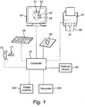
- figure 1 of the '527 patent a schematic diagram is shown showing various components that can be included in various embodiments for the synthesis of patterns and/or for the analysis of patterns with the super-formula operator.
- shapes or waves can be "synthesized" by the application of the following exemplary basic steps:
- a choice of parameters is made (e.g., by either inputting values into the computer 10, i.e., via a keyboard 20, a touch screen, a mouse-pointer, a voice recognition device or other input device or the like, or by having the computer 10 designate values), and the computer 10 is used to synthesize a selected super-shape based on the choice of parameters.
- the super-formula can be used to adapt the selected shapes, to calculate optimization, etc.
- This step can include use of: graphics programs (e.g., 2D, 3D, etc.); CAD software; finite element analysis programs; wave generation programs; or other software.
- the output from the first or second step is used to transform the computerized super-shapes into a physical form, such as via: (a) displaying the super-shapes 31 on a monitor 30, printing the super-shapes 51 upon stock material 52 such as paper from a printer 50 (2-D or 3-D); (b) performing computer aided manufacturing (e.g., by controlling an external device 60, such as machinery, robots, etc., based on the output of step three); (c) generating sound 71 via a speaker system 70 or the like; (d) performing stereo lithography; (e) performing rapid prototyping; and/or (f) utilizing the output in another manner known in the art for transforming such shapes.
- the '527 patent discusses both synthesis (such as, e.g., creation of shapes) and analysis (such as, e.g., the analysis of shapes). With respect to analysis, the '527 patent explains that: "In general, although not limited thereto, shapes or waves can be "analyzed” by the application of the following basic steps (these steps have similarities to the foregoing steps in synthesis in reverse): In a first step, a pattern can be scanned or input into a computer (e.g., in a digital form).
- an image of an object can be scanned (2-D or 3-D), a microphone can receive sound waves, or electrical signals (e.g., waves) can be input, data from a computer readable medium such as, e.g., a CD-ROM, a diskette, an internal or external flash drive, etc., can be input, data can be received on-line, such as via the Internet or an Intranet, etc.
- a computer readable medium such as, e.g., a CD-ROM, a diskette, an internal or external flash drive, etc.
- data can be received on-line, such as via the Internet or an Intranet, etc.
- Various other known input techniques could be used, such as, for example, using digital or other cameras (e.g., whether single picture or continuous real time, etc.), etc.
- an image scanner 100 e.g., a document scanner utilized to scan images on stock material such as paper or photographs, or another scanner device
- a recorder 200 e.g., which receives waveforms via a microphone or the like
- the computer can include a library or catalogue (e.g., stored in a memory) of primitives (e.g., categorizing assorted supershapes by parameter values).
- the computer can then be used to approximate, identify, classify and/or the like the supershapes based on the information in the library or catalogue.
- the catalogue of primitives could be used, for example, for the first approximation of patterns or shapes.
- the analyzed signals can be moderated as desired (e.g., operations can be performed similar to that described above with reference to the second general phase or step of synthesis).
- an output can be created.
- the output can include: (a) providing a visual (e.g., displayed or printed) or an audible (e.g., sound) output; (b) controlling the operation of a particular device (e.g., if certain conditions are determined); (c) providing an indication related to the analyzed pattern (e.g., identifying it, classifying it, identifying a preferred or optimal configuration, identifying a defect or abnormality, etc.); (d) creating another form of output or result as would be apparent to those in the art.
- the computer proceeds using a certain type of representation. If it is a chemistry pattern, the XY graph should be selected. If it is a closed shape, a modified Fourier analysis should be selected.
- the computer should be adapted (e.g., via software) to provide an estimation of the right parameters for the equation to represent the digitized pattern.
- the international patent application WO2011/1615 discloses a method of synthesizing or analyzing a shape, by using the formula as described in the '527 patent as referred to above, dependent on the shape or geometry of the environment surrounding said shape.
- An object of some embodiments of the invention is to find a class of products in which the above technology is implemented in a beneficiary manner.
- improved lens antennas for a wide class of wireless applications (including Wi-Fi networks) are invented.
- the proposed antennas are extremely simple to construct, easily machinable and thus cheap, they surprisingly considerably outperform antennas currently used in wireless communications in terms of operational bandwidth, maximum gain, and radiation pattern agility. Furthermore, the considered antennas use sustainable technology and are ecologically friendly.
- the geometry of a base profile of the lens and/or ground plane is defined by the polar equation known in the scientific literature as superformula (or Gielis' formula) and its generalization to three-dimensional spaces.
- the superformula is explained in detail in the above-noted U.S. Patent No. 7,620,527 to J. Gielis .
- Such equation provides the capability for unified description of natural and abstract shapes ranging from elementary particles to complex generalized Lamé curves.
- the invented antenna allows an increased number of degrees of freedom for the design, paving the way towards a wide variety of radiating structures and sensors with tunable electromagnetic characteristics.
- the United States patent application US2010/0220031 discloses a wideband dielectric antenna comprising a ground plane onto which a dielectric structure is mounted, wherein multiple feeding strips acting as probes are attached to an outer surface of said dielectric structure.
- the antennas used as the most front-end devices, are becoming more important in terms of satisfying challenging requirements, such as miniaturized size, improved radiation and bandwidth performances and ease of fabrication and integration.
- printed circuit microwavestrip
- metallic rods monopole
- the proposed supershaped lens antennas provide clear advantages in reason of their reduced losses (virtually no metal loss), high radiation efficiency and ease of integration with planar circuitry.
- they offer a high degree of flexibility and versatility over a wide frequency range, allowing for the designer to suit various requirements.
- every lens antenna comprises a lens and/or ground plane having a three-dimensional shape. It can be favourable that multiple base profiles of the lens and/or ground plane are substantially supershaped, wherein each supershaped base profile is defined by the polar function (superformula) according to claim 1. In this manner three-dimensional a supershaped lens and/or supershaped ground plane will be created, which will commonly be in favour of the power distribution pattern and intensity of the lens antenna as such.
- a first base profile is defined according to the superformula according to claim 1
- at least one further base profile is defined according to the superformula according to claim 1.
- Both base profiles commonly define a cross-section of the final supershape, o-in other words - the first base profile defines a profile while the other base profile defines a path along which this first base profile is rotated.
- the three-dimensional shape can be the result of a superposition of multiple two-dimensional shapes. For example, square base profile combined with a triangular base profile leads to a pyramid shape, while a teardrop shaped base profile combined with a rectangular base profile leads to a wing shape. In this manner, an infinite number of three-dimensional supershapes can be created.
- the three-dimensional shape can also be the result of combining outer surface faces, each face complying with the superformula according to claim 1.
- a dodecaeder has pentagon shaped faces, wherein each pentagon complies with the two-dimensional superformula according to claim 1.
- each pentagon complies with the two-dimensional superformula according to claim 1.
- each distinctive face is defined by a triangle complying with the superformula.
- the design of a supershaped lens antenna is carried out by assimilating it to an ordinary cylindrical dielectric resonator antenna.
- the lens height (h d ) is chosen to be about a wavelength in the dielectric material at the central operating frequency of the antenna (f c ), that is: h d ⁇ c 0 f c ⁇ I with c 0 being the speed of light in vacuum, and where ⁇ r denotes the relative permittivity of the material forming the lens.
- the location and the length of the probe are heuristically determined by full-wave analysis.
- the electromagnetic lens in particular formed by the ground surface or bottom surface of the lens (commonly parallel to the ground plane), and/or the ground plane has at least one base profile, which is substantially supershaped, wherein m ⁇ 4.
- a further preferred boundary condition is that a ⁇ b, and preferably that at least one value of n x , n y , and no deviates from 2. Also these boundary conditions lead to unconventionally shaped lens. The above also applies to the ground plane.
- the ground plane can either be flat or non-planar, such as curved and/or angulated.
- both the lens and the ground plane, together forming a so-called transducer have a base profile which complies to the superformula as stated above.
- the ground plane and the lens have equivalent shapes, or base profiles with an equivalent shape.
- the shape of the ground plane can be completely different from the shape of the lens, provided that at least one base profile of at least one of the ground plane and the lens complies with the superformula as formulated in claim 1.
- the substantially supershaped base profile is a base profile of the lens which extends in a direction which is substantially parallel to a plane defined by the ground plane.
- This will commonly lead to an axis of symmetry of the lens which is oriented perpendicular to a (central) plane defined by the ground plane which is in favour of the spatial power density distribution.
- This embodiment allows the application of a lens having the (unconventional) shape of a polyhedron, such as a prism, wherein an n-sided polygonal base of the polyhedron is directed towards and eventually mounted onto the ground plane.
- the antenna according to the invention can be used to receive and/or to transmit electromagnetic radiation.
- the functionality of the probing structure therefore depends on the desired functionality of the antenna. It is thus thinkable that the probing structure is configured to receive and/or to transmit electromagnetic radiation.
- the probing structure comprises at least one probe.
- the geometry, including the shape and dimensioning, of the probe is commonly completely dependent on the specific purpose and application of the antenna. Different types of probes can be used.
- a well known probe is a coaxially fed probe, which probe is at least partially accommodated within the lens, wherein the probe is thus at least partially surrounded by the lens.
- the lens is commonly provided with an accommodating space for accommodating the probe.
- the probe can also be formed by a waveguide which does not extend into the lens and merely connects to a base plane of the lens.
- the probe can be formed by a microstrip which extends to a base plane of the lens.
- the probe is formed by a patch which is positioned between the ground plane and the lens. Application of a patch will commonly propagate generation of a spherical wave front and therefore a substantially homogenous power density distribution within the lens. Hence, different types of probes can be used in the lens antenna according to the present invention.
- the antenna will be suitable to operate within a single designated frequency band.
- the frequency range of said frequency band completely depends on the application of the antenna.
- GSM 900/1800/1900 bands (890-960 MHz and 1710-1990 MHz); Universal Mobile Telecommunication Systems (UMTS) and UMTS 3G expansion bands (1900-2200 MHz and 2500-2700 MHz); frequency bands in the microwave spectrum (1-100 GHz), in particular the K a band (26.5-40 GHz) and the K u band (12-18 GHz) used for satellite communication; and Wi-Fi (Wireless Fidelity)/Wireless Local Area Networks (WLAN) bands (2400-2500 MHz and 5100-5800 MHz).
- the lens antenna according to preferred embodiments of the invention is, however, not limited to the abovementioned enumeration of well-known frequency bands.
- a multiband antenna in a mobile communication system can be defined as the antenna operating at distinct frequency bands, but not at the intermediate frequencies between bands.
- the probing structure comprises multiple probes leading to multiple antenna ports. The operation of these probes can be reconfigurable. In recent years, a growing effort has been devoted by the industrial and scientific research communities in the development of reconfigurable antennas.
- the adopted multiple feeding mechanism allowing for an easy wide-range tuneability of the antenna performance, has to be optimized in such a way as to minimize the level of spurious electromagnetic coupling between the antenna ports (probes), potentially resulting in a degradation of the device performance.
- the considered device is in fact acting as an antenna at those frequencies where the input power reflection level is not perfectly compensated by the transmission coefficients between the different ports.
- the device behaviour can be described as the superposition of the natural responses of decoupled one-port junctions, where the n- th junction presents a positive reflection coefficient ⁇ n .
- the circuital characteristics, as well as the radiation properties of the antenna are primarily defined by the singular values of the relevant scattering matrix.
- these antennas can also be used in arrays, not only planar arrays but also in tailored 3D arrays, based on 3D supershapes.
- the considered class of lens antennas can be optimized for the design of inexpensive arrays for next-generation wireless radar, space applications with demanding requirements in terms of impedance matching and radiation properties.
- the adoption of non-uniformly spaced planar arrays is envisaged.
- Proper shaping of the radiation pattern with a reduced number of antenna elements leads to reduced weight, cost, and complexity of the feeding network.
- a larger average inter-element distance results in a smaller parasitic antenna coupling level. Due to the aperiodic spacing, no replicas of the antenna main lobe occur in the visible space, even where pattern scanning is performed.
- both amplitude and phase of each antenna element are to be controlled. Combined amplitude and phase control can be used to adjust side lobe levels and steer nulls better than can be achieved by phase control only.
- the geometry includes both the shape and the dimensioning of the probes.
- the preferred length of the probe is dependent on both the material of the lens, in particular the dielectric constant of the material of the lens, and the desired frequency or frequency band.
- the length of the probe is preferably between 4 and 8 mm.
- the length of said probe would preferably be between 10 and 18 mm.
- the diameter of the at least one probe is preferably situated between 1 and 3 mm.
- mutual coupling When identical antenna elements are placed in an array or multiple different antennas are used, they interact with each other. This interaction between elements due to their close proximity is called mutual coupling, which affects the input impedance as well as the radiation pattern. It is noted previously that in base station applications, more than one similar antenna can be implemented to either acquire higher gain with array structures or at least provide dual-polarization with two antenna probes. Furthermore, in mobile station applications, even multiple different antennas can be used in a limited available space to provide multiband operation. For these antenna systems, the mutual coupling is simply defined as the interference value between two antenna probes, which is desired to be as low as possible.
- the mutual orientation of at least two probes is such that said probes are positioned at least partially out of the electromagnetic line of sight of each other. Because the probes do not see each other, the electromagnetic interference within the lens is kept to a minimum. Positioning the probes out of the line of sight of each other can be realised, for example, by positioning a separate reflective element between the probes. This reflective element can be enclosed by the lens. However, application of such a separate reflective element will commonly affect the efficiency of the antenna. It is therefore preferred that the electromagnetic radiation transmitted by at least one probe is at least partially reflected by at least one circumferential wall of the lens in a direction away from the at least one other probe.
- the circumferential wall of the lens is preferably at least partially concavely shaped which facilitates interruption of the line of sight of the probes.
- the circumferential can be at least partially corrugated to propagate reflection of electromagnetic radiation transmitted by a probe in a direction away from the at least one other probe.
- in the superformula m is preferably equal or larger than 4, which allows it to position the probes in the (circumferential) sharp edges of the lens to minimize mutual interference of the probes.
- the probe is accommodated within an accommodating space of the lens. The positioning of these accommodating spaces is preferably such that the probes will be positioned out of the line of sight.
- the lens antenna according to the invention can be dimensioned relatively compactly if compared to conventional antennas.
- the height of the lens is preferably smaller than or equal to 5 cm which will commonly sufficient to allow proper functioning of the lens antenna according to the invention.
- the lens is preferably at least partially made of a dielectric material, more preferably a dielectric material having a dielectric constant of between 2 and 90. By choosing a material having a relatively high dielectric constant, the size of the lens can be reduced significantly. It is possible that the lens is at least partially made of at least one ceramic. Dielectric constants (e) of ceramics span from 4.5 to 100. Dielectrics with ⁇ ranging from 4.5 to about 6 are typically based on magnesium aluminium silicate and magnesium silicate compounds, respectively. Dielectrics with ⁇ in the 13 to 16 range are based on the compounds Mg 2 TiO 4 and MgTiO 3 . Several routes can be followed to obtain low loss ceramics with ⁇ > 16.
- CaTiO 3 shows relatively modest loss but has a high ⁇ (150 - 160) and a very large, negative temperature coefficient of ⁇ (about -1600 ppm/°C).
- CaTi O 3 is chemically compatible with both Mg 2 TiO 4 ( ⁇ 13) and MgTiO 3 ( ⁇ 16).
- the magnesium titanates have moderately positive temperature coefficients of ⁇ .
- composite ceramics composed of Mg 2 TiO 4 plus CaTiO 3 can cover ⁇ from 13 to about 150 at any desired value while composites of MgTiO 3 plus CaTiO 3 cover almost the same range, 16 to about 150.
- Low loss ceramics covering ⁇ from about 37 to about 100 also can be produced from barium titanates.
- the low end of the series is the compound, BaTi 4 O 9 .
- Small increases in the TiO 2 content yield BaTi 4 O 9 / Ba 2 Ti 9 O 20 ceramic composites or pure Ba 2 Ti 9 O 20 .
- the ⁇ remains in the 37-39 range and temperature coefficient of ⁇ remains very small but slightly negative.
- the lens is at least partially made of glass, in particular Pyrex ® (a clear, low-thermal-expansion borosilicate glass commercially available from Corning Incorporated), crystal, silica (silicon dioxide), ferroelectric dielectric materials, liquid crystals, at least one polymer, in particular polyvinylchloride (PVC), polystyrene (PS), polyimide (PI), a bioplastic (a plastic derived from renewable biomass sources, such as vegetable fats and oils, corn starch, pea starch or microbiota), or fluoroplastics; and/or a metal oxide, in particular titanium oxide, aluminium oxide, barium oxide, or strontium oxide.
- Pyrex ® a clear, low-thermal-expansion borosilicate glass commercially available from Corning Incorporated
- crystal silica (silicon dioxide), ferroelectric dielectric materials, liquid crystals
- at least one polymer in particular polyvinylchloride (PVC), polystyrene (PS),
- the application will commonly be prepared both from a financial point of view and from a design point of view.
- Polymers are relatively cheap, and moreover easy to shape using conventional moulding, extrusion and/or thermoforming techniques, and can even be shaped by way of 3D printing which provides a significant freedom of design.
- a lens comprising a shell which is at least partially made of at least one glass, crystal, and/or at least one polymer enclosing at least one inner space which is at least partially filled with a fluid, preferably air or demineralised water (acting as dielectric).
- a fluid preferably air or demineralised water (acting as dielectric).
- the lens can be a dielectric resonator leading to a dielectric resonator antenna (DRA).
- Electromagnetic radiation are introduced as radio waves into the inside of the resonator material from a transmitter circuit, wherein the waves bounce back and forth between the resonator walls, forming standing waves.
- the walls of the resonator are partially transparent to radio waves, allowing the radio power to radiate into space.
- a surface of the ground plane directed towards the lens is at least partially reflective.
- the ground plane could be flat or curved (cup-shaped or bowl-shaped) and comprises an electrically conducting surface to reflect the electromagnetic radio waves from other antenna elements.
- the plane does not necessarily have to be connected to ground.
- the conducting surface must be at least a quarter of the wavelength ( ⁇ /4) of the radio waves in size.
- the ground plane can be formed e.g. by a metal disc or a screen.
- the metal skin of a car or aircraft can serve as a ground plane for whip antennas projecting from it.
- the ground plane doesn't have to be a continuous surface.
- the "plane” In the ground plane antenna the "plane” consists of several wires ⁇ /4 long radiating from the base of a quarter wave whip antenna.
- the radio waves from the lens (or from another antenna) that reflect off a ground plane appear to come from a mirror image of the antenna located on the other side of the ground plane.
- the radiation pattern of the monopole plus the virtual "image antenna” make it appear as a two element centre-fed dipole antenna. So a monopole mounted over an ideal ground plane has a radiation pattern identical to a dipole antenna.
- the feed line from the transmitter or receiver is connected between the bottom end of the monopole element and the ground plane.
- the ground plane preferably has good conductivity; any resistance in the ground plane is in series with the antenna, and serves to dissipate power from the transmitter.
- the ground plane could be combined with a printed circuit board (PCB). This serves to make circuit design easier, allowing the designer to ground any component without having to run additional copper traces; component copper wire needing grounding is routed directly through a hole in the board to the ground plane on another layer.
- the large area of copper also conducts the large return currents from many components without significant voltage drops, ensuring that the ground connection of all the components are at the same reference potential.
- the major reason for using large ground planes is commonly to reduce electrical noise and interference being coupled from one part of the circuit to another through the ground (ground loops), and crosstalk between adjacent circuit traces.
- ground plane under printed circuit traces can reduce crosstalk between adjacent traces.
- an electrical signal in one can be coupled into the other through electromagnetic induction by magnetic field lines from one linking the other; this is called crosstalk.
- crosstalk When a ground plane layer is present underneath, it forms a transmission line (stripline) with the trace. The oppositely-directed return currents flow through the ground plane directly beneath the trace. This confines the electromagnetic fields to the area between the trace and the ground plane, reducing crosstalk.
- the directivity pattern is a result of the difference between the phase velocity of propagation of an electromagnetic wave in air and that in the lens material (n ⁇ 1).
- the shape of the lens depends on the refractive index n (the ratio of the phase velocity of propagation of a radio wave in a vacuum to that in the lens).
- n the ratio of the phase velocity of propagation of a radio wave in a vacuum to that in the lens.
- a decelerating lens antenna, as in optics, is one for which n > 1.
- the lens of these kinds of antennas are preferably made of high-quality low-loss homogeneous dielectrics, such as polymers.
- the probing structure preferably comprises at least one first probe configured to communicate in a first frequency band, and at least one second probe configured to communicate in a second frequency band, which allows the antenna to be implemented in a Multiple Input Multiple Output (MIMO) system.
- MIMO technology has recently developed as a new technology to achieve very high bandwidth efficiencies and larger data rates in modern wireless communications.
- MIMO technology multiple antennas are placed at the input and output side of a communication system to improve the channel capacities.
- the multidimensional statistical behaviour of the MIMO fading channel and the design parameters of the antennas that are taken at the transmitter and receiver side are responsible for the improvement of data rates.
- Multiple Input Multiple Output (MIMO) technology is the latest paradigm, where multiple antennas are used at both transmitter and receiver to improve communication performance.
- MIMO technology has attracted attention in wireless communications, because it offers significant increase in data throughput, channel capacity and link range without additional bandwidth or increase transmitted power. Because of these properties, MIMO is an important part of modern wireless communication standards such as IEEE802.11n (Wi-Fi), 4G, 3GPP long term evolution, WiMAX (Wireless interoperability for microwave access) and HSPA (High Speed Packet Access) etc.
- Wi-Fi Wi-Fi
- 4G 3GPP long term evolution
- WiMAX Wireless interoperability for microwave access
- HSPA High Speed Packet Access
- the antenna comprises at least one processor to automatically switch the probing structure between a radiation transmitting mode and a radiation receiving mode for two-way communication of the probing structure. More particularly, the processor is preferably configured to automatically switch between the first frequency band and the second frequency band for two-way communication in each frequency band.
- the preferred embodiments of the invention also relate to an antenna system for transmitting and receiving electromagnetic signals comprising at least one antenna according to the invention.
- the antenna system comprises a plurality of MIMO-configured antennas as described above, wherein each antenna comprises multiple probes.
- the system preferably also comprises at least two multi-band antennas, and at least one processor for switching in at least one of the frequency bands, so ensuring diversity of reception and transmission of the signals in this band.
- a processor is configured to control switching means, wherein the switching means is a SPDT (Single Port Double Throw) switch or a DPDT (Double Port Double Throw) switch.
- the system further comprises at least one interface means for programming the at least one processor, and therefore for programming (configuring) the antenna as such.
- the invention further relates to a method of manufacturing an antenna according to the invention, comprising:
- step B) preferably multiple probes are connected to the ground plane and/or the lens. At least one probe is preferably configured to communicate in a first frequency band and at least one other probe is configured to communicate in a second frequency band. More preferably, the different probes are oriented such that, during operation, different sectors of the lens will be excited. It is favourable in case the probes are positioned out of the line of sight in order to counteract mutual coupling.
- the invention further relates to a method for use in wireless communications by using an antenna according to the invention, the method comprising the step of connecting a communication circuit to an antenna network, the network comprising a plurality of antennas according to the invention, each antenna optimized for operation in at least one designated frequency band.
- the optimization of the antenna geometry and material completely depends on the specific purpose.
- the communication circuit commonly comprises a transmitter and/or a receiver which in combination form a transceiver.
- Each antenna is preferably optimized for operation in multiple frequency bands, wherein each probe is configured to operate within a designated (single) frequency or frequency band.
- the antennas can be connected either in parallel or in series.
- the invention additionally relates to a lens as used in an antenna according to the invention.
- the invention also relates to a ground plane as used in an antenna according to the invention. Advantages and embodiments of these antenna components have been described above in a comprehensive manner.
- a still further embodiment of the present invention refers to an RF transceiver of a wireless communications device, wherein an antenna according to the invention is employed.
- the invention refers to an electronic device having a wireless interface which comprises an RF transceiver as described above.
- shapes or waves of a ground plane and/or a lens of an antenna according to the invention can be "synthesized" by the application of the following exemplary basic steps:
- steps 1 and 2 are also schematically illustrated in the schematic diagram shown in FIG. 2 (steps 1 and 2 being capable of being carried out within the computer itself as shown).
- FIG. 17 of US 7,620,527 corresponds to FIG. 17 of US 7,620,527 .
- a number of exemplary embodiments of pattern "synthesis" with the super-formula are described in further detail.
- the present invention has great utility in 2-D graphic software applications.
- the present invention can be applied, for example, in conventional commercial programs such as Corel-DrawTM and Corel-PaintTM, Open Office applications, SupergraphxTM for Adobe Illustrator and PhotoshopTM, Adobe PhotoshopTM, in various drawing programs in Visual BasicTM or WindowsTM, or in other environments like, for example, Lotus WordProTM and Lotus Freelance GraphicsTM, JavaTM, Visual CTM, Visual C++TM and all other C-environments.
- the present invention has substantial advantages in image synthesis because, among other things, the present approach enables a substantial savings in computer memory space because only the super-formula with classical functions (such as powers, trigonometric functions, etc.) needs to be utilized.
- the present invention has great utility in 3-D graphic software applications (as well as in representations in various other dimensions).
- the present invention can be applied, for example, in Computer Aided Design (“CAD”) software, software for Finite Element Analysis (“FEM”), Supergraphx 3D Shape Explorer, antenna design and analysis software, such as CST, Ansoft HFSS, Remcom XFdtd, EMSS Feko, Empire XCcel, architectural design software, etc.
- CAD Computer Aided Design
- FEM Finite Element Analysis
- Supergraphx 3D Shape Explorer such as CST, Ansoft HFSS, Remcom XFdtd, EMSS Feko, Empire XCcel, architectural design software, etc.
- the present invention allows, for example, one to use single continuous functions, rather than spline functions, for various applications.
- Industrial applications of CAD include, e.g., use in Rapid Prototyping or in Computer Aided Manufacturing (“CAM”) including 3D printing.
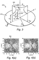
- FIG. 3 wherein an embodiment of a lens antenna 300 according to preferred embodiments of the invention is shown.
- the antenna 300 comprises a ground plane 301, an electromagnetic lens 302 mounted to said ground plane 301, and a probing structure of which merely a probe 303 is shown.
- the lens 302 has a prismatic shape which complies with the superformula.
- the lens 302 is made of PVC in this example.
- the lens 302 is provided with an accommodating space 304 for accommodating the probe.
- the ground plane 301 is made of metal. Both the probe 303 and the ground plane 301 are connected, commonly via a control circuit (not shown), to an electrical power source, such as a battery (DC) or mains (AC).
- DC battery
- AC mains
- the lens 302 in this embodiment acts as dielectric resonator which makes the lens antenna 300 a dielectric resonator antenna (DRA). Since the lens 302 complies with the superformula, this antenna 300 can also be considered as a supershaped antenna (S-DRA).
- the circular metal plate acting as ground plane 301 has a radius plane.
- the antenna 300 is fed from the bottom side by means of a coaxial connector turning, at the ground plane level, into the electric probe 303 of length h p and diameter d p . The probe is located at (xp, yp, 0).
- the metal ground plane 301 has a radius pg and a thickness tg.
- ⁇ d ( ⁇ ) is a curve located in the XY-plane and ⁇ ⁇ [0, 2pi) is the angular coordinate.
- ⁇ d ( ⁇ ) is a curve located in the XY-plane
- ⁇ ⁇ [0, 2pi) is the angular coordinate.
- PVC used for the lens 302 in this illustrative example is a thermoplastic polymer produced in enormous quantities in reason of low cost and ease of processing. Moreover, PVC is extremely durable and resistant to chemical corrosion and thus very well adapted to outdoor applications. Additionally, PVC can be blended with different materials providing a wide range of physical properties. The use of PVC can then result in an inexpensive option for manufacturing intricately shaped dielectric resonator/lens antennas by using conventional drilling/milling or more advanced three-dimensional printing techniques. This is furthermore of significant importance in order to enhance the aesthetic quality of the proposed radiating structures when used for wireless communications in habitable structures such as residential units, office buildings, theaters, stadiums, etc.
- three-dimensional solid objects are formed using an additive process in which successive layers of material are laid down one upon the other to create desired.
- plastics including bioplastics and combinations of plastics, depending on the dielectric constants of the material.
- various other materials can be employed to produce antennas in a highly sustainable way.
- antennas with dynamic shape changes to modify its behaviour for specific purposes using liquid components (such as liquid crystals) can be employed, with the dynamics of shape changes modified by mechanical or electronic steering, or making use of other physical forces.
- the shape of the lens 302 is such that a relatively good power density distribution in preferred directions can be obtained as when compared with such a distribution in case a cylindrical lens would be used (see FIG. 4(a) , showing an exemplary embodiment of the invention, and 4(b), showing an example of a cylindrical lens).
- the radiation properties of supershaped lens antennas can be investigated by means of a dedicated asymptotic technique based on optical ray approximation.
- Geometrical Optics is adopted to analyze the electromagnetic field propagation within the lens region.
- the contribution of the multiple internal reflections is properly taken into account, so enhancing the accuracy of the modelling procedure especially where dielectric materials with relatively large permittivity are used in the design since, in this case, the common hypothesis that the energy content relevant to higher order reflected rays can be neglected is not applicable.
- the electromagnetic field outside the lens can be evaluated by radiation in free space of the equivalent electric and magnetic current distributions along the interface with the air region.
- these currents are determined by application of the local Fresnel transmission coefficients along the surface of the lens to the Geometrical Optics field in accordance with the Physical Optics method.
- the adoption of the Gielis' formula translates into the possibility of automatically reshaping the lens profile so that any automated optimization procedure, such as Genetic Algorithms, Neural Networks, Particle Swarm Optimation, and Ant Colony Optimization, can be applied in order to identify the geometrical parameters yielding optimal antenna performance.
- E ⁇ t ⁇ m E ⁇ t m
- E ⁇ t m ⁇ E ⁇ t m ⁇ e j ⁇ E ⁇ t m n ⁇ ⁇ k ⁇ t m ⁇ k ⁇ t m ⁇ n ⁇ ⁇ k ⁇ t m ⁇ k ⁇ t m ⁇ + E t ⁇ m n ⁇ ⁇ k ⁇ t m ⁇ n ⁇ ⁇ k ⁇ t m ⁇ denoting the electric field contribution pertaining to the internal reflection process of order m.
- n ⁇ denotes the normal to the surface of the lens
- E ⁇ t m and E t ⁇ m are the parallel and orthogonal components, respectively, of the transmitted wave contribution due to the m -th reflected beam.
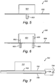
- FIGs. 5-9 show schematic views of different antenna constructions according to illustrative embodiments of the invention.
- FIG. 5 shows a single-band antenna 500 that comprises a supershaped lens 501, a reflective supershaped ground plane 502 connected to said lens 501, and a waveguide 503 for feeding electromagnetic radiation into the lens 501 and/or for receiving electromagnetic radiation from the lens 501.
- FIG. 6 shows a dual-band antenna 600 comprises a supershaped lens 601 enclosing two different probes 602, 603 having mutually distinctive geometries.
- the lens 601 and the probes 602, 603 are connected to a flat ground plane 604.
- a flat ground plane 604 instead of a flat ground plane 604 also a curved or otherwise shaped ground plane 604 can be used.
- Each of the probes 602, 603 extends from a coaxial connector 605, 606 which connector is also connected to said ground plane 604.
- the lens 601 is made of silicon in some examples.
- the shortest probe 602 is configured to operate within a frequency band of 2.4 GHz, while the longest probe 603 is configured to operate within a frequency band of 5 GHz, which makes this compact antenna 600 well suitable to serve as dual-band Wi-Fi-antenna.
- FIG. 7 shows a single-band antenna 700 that comprises a lens 701, and a reflective supershaped ground plane 702 connected to said lens 701, wherein the ground plane 702 is provided with a central hole 703 forming a slot or cavity between the lens 701 and a dielectric printed circuit board (PCB) 704 to which the ground plane 702 is attached.
- PCB printed circuit board
- a rear side of the PCB 704 is provided with a electrically conductive microstrip 705.
- a static planar wave front will be formed between the microstrip 705 and the ground plane 702 which will wave front will enter the lens 701 via the central hole 703 and will turn into a spherical wave front within the lens 701.
- the electromagnetic radiation within the lens 701 will be internally reflected and excited in a controlled manner, dependent on the (super)shape of the lens 701 and eventually the supershape of the ground plane 702. This mechanism is also called a slot fed antenna.
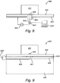
- FIG. 8 shows a single-band antenna 800 that comprises a supershaped lens 801, which lens 801 is connected to a laminate of an insulating layer 802 and an electrically conductive layer 803 acting as ground plane.
- the electrically conductive layer 803 provided with a central hole 804 through which a central probe 805 extends.
- An outer end of the probe 805 is connected to a conductive patch 806 which is positioned within the lens 801 and which is configured to couple electromagnetic into and/or out of the lens 801.
- the probe 805 is also connected to control circuit 807 including a processor. Both the probe 805 and the electrically conductive layer 803 are connected to an AC power source 808.
- the control circuit 807 is configured to be programmed by means of a computer interface 809 which allows a user to define the purpose of the antenna 800 (transmitting signals, receiving signals, or both) and further characteristics of the antenna 800 such as the frequency band which is used by the antenna 800.
- this antenna can also be provided with multiple probes and patches in order to allow the antenna to operate simultaneously at different frequencies and/or different frequency bands.
- FIG. 9 shows a single-band antenna 900 that comprises a supershaped dielectric resonator 901, which resonator 901 is connected to a laminate of a first insulating layer 902, an electrically conductive layer 903 acting as ground plane, a second insulating layer 904, and a microstrip 905.
- the resonator 901 is made of PVC or Teflon® or a combination/mixture of polymer and ceramics.
- an electrically conductive patch 906 is provided within the resonator 901 and onto the first insulating layer 902 .
- the patch 906 can either have a flat geometry or a supershaped geometry.
- the ground plane 903 is made of metal and/or an electrically conductive polymer and is provided with a central hole 907, and the microstrip 905 extends such that an outer end will be positioned in line with the patch 906.
- a power source 908 By connecting the microstrip 905 and the (intermediate) ground plane 903 to a power source 908 an electromagnetic planar wave front will be formed between the microstrip 905 and the ground plane 903 which will excite the patch 906 in such a manner that spherical wave front is propagated into the lens.
- the antenna 900 can make part of an electronic device 909, such as e.g. a router, a notebook, or a mobile phone.
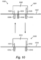
- FIG. 10 shows a MIMO-configured antenna system 1000 according to some embodiments of the invention, comprising multiple antennas 1001, 1002 according to the invention, wherein said antennas 1001, 1002 are configured to communicate with each other wirelessly in two directions.
- a first antenna 1001 comprises multiple probes 1003, 1004, 1005, wherein two probes 1003, 1004 have an identical geometry and are configured to operate within the same first frequency band, while the other probe 1005, having a different geometry, is configured to operate within another second frequency band.
- the probes 1003, 1004, 1005 are enclosed by a supershaped lens 1006 which is supported by a ground plate 1007.
- the probes make part of coaxial connectors 1008, 1009, 1010 which are connected to a control circuit (not shown).
- the other antenna 1002 comprises two probes 1011, 1012, wherein a first probe 1011 is configured to operate within the first frequency band, and the other probe 1012 is configured to operate within the second frequency band.
- the probes 1011, 1012 are enclosed by a supershaped lens 1013 which is supported by a ground plate (ground plane) 1014.
- the probes make part of coaxial connectors 1015, 1016 which are connected to a control circuit (not shown).
- FIG. 11 shows a cross-section of a lens antenna 1100 according to some embodiments of the invention.
- the antenna 1100 comprises a reflective ground plane 1101 onto which a supershaped lens 1102 is positioned.
- the shape of the lens 1102 is comparable or even identical to the shape of the lens 302 as shown in FIG. 3 .
- a circumferential wall 1103 comprises of four concave wall parts 1103a, 1103b, 1103c, 1103d connected to each other, as a result of which four corners 1104a, 1104b, 1104c, 1104d are defined.
- One of the concave wall parts 1103a is provided with a selective corrugated profile.
- the lens 1102 is made of a dielectric material.
- the antenna 1100 comprises two probes 1105, 1106, wherein each probe 1105, 1106 is positioned in a corner 1104, 1104b of the lens 1102.
- the positioning of the probes 1105, 1106 is such that the probes are not in the line of sight of each other (simplified shown by the dashed line A).
- Electromagnetic radiation excited by a probe 1105, 1106 will be reflected (see arrows) by the wall parts 1103a, 1103b, 1103c, 1103d, and in particular by the intermediate corrugated wall parts 1103a, in a direction away from the other probe 1105, 1106 so that mutual coupling and hence interference can be counteracted.
- inventive concepts are illustrated in a series of examples, some examples showing more than one inventive concept. Individual inventive concepts can be implemented without implementing all details provided in a particular example. It is not necessary to provide examples of every possible combination of the inventive concepts provide below as one of skill in the art will recognize that inventive concepts illustrated in various examples can be combined together in order to address a specific application.
- the terminology “present invention” or “invention” can be used as a reference to one or more aspect within the present disclosure.
- the language present invention or invention should not be improperly interpreted as an identification of criticality, should not be improperly interpreted as applying across all aspects or embodiments (i.e., it should be understood that the present invention has a number of aspects and embodiments), and should not be improperly interpreted as limiting the scope of the application or claims.
- the terminology “embodiment” can be used to describe any aspect, feature, process or step, any combination thereof, and/or any portion thereof, etc. In some examples, various embodiments can include overlapping features.
- abbreviated terminology can be employed: “e.g.” which means “for example.”
Landscapes
- Physics & Mathematics (AREA)
- Electromagnetism (AREA)
- Engineering & Computer Science (AREA)
- Computer Networks & Wireless Communication (AREA)
- Signal Processing (AREA)
- Aerials With Secondary Devices (AREA)
- Variable-Direction Aerials And Aerial Arrays (AREA)
- Transceivers (AREA)
- Support Of Aerials (AREA)
- Control Of Motors That Do Not Use Commutators (AREA)
Description
- The invention relates to a lens antenna. The invention also relates to an antenna system for transmitting and receiving electromagnetic signals comprising at least one antenna according to the invention. The invention further relates to a method of manufacturing an antenna according to the invention. The invention moreover relates to a method for use in wireless communications by using an antenna according to the invention. The invention additionally relates to an RF transceiver of a wireless communications device comprising at least one antenna according to the invention. The invention further relates to an electronic device comprising an RF transceiver according to the invention.
- The present invention improves upon the subject matter disclosed in
U.S. Patent No. 7,620,527 issued on Nov. 17, 2009 to a present inventor, Johan Gielis. - The '527 Patent describes systems and methods by which patterns (e.g., such as images, waveforms such as sounds, electromagnetic waves, or other signals, etc.) are synthesized, modulated and/or analyzed through the use of a computer programmed with a novel mathematical formula. The formula can be used to create a variety of shapes, waveforms, and other representations. The formula greatly enhances ability in computer operations and provides a great savings in computer memory and a substantial increase in computing power.
- The geometric concept of the '527 patent is useful for modeling and for explaining why certain natural shapes and forms grow as they do. As explained in the '527 patent, the inventor therein found that most geometrical forms and regular shapes, including circles and polygons, can be described as special realizations of the following formula:

- The '527 patent explains how this formula and representations thereof can be utilized, for example, in both the "synthesis" and "analysis" of patterns (i.e., including for example image patterns and waveforms such as electromagnetic (e.g., electricity, light, etc.), sound and other waveforms or signal patterns) and the like.
- In order to synthesize various patterns, the parameters in this equation can be modified so that a variety of patterns can be synthesized. Notably, the parameters appearing in the equations above can be moderated. By moderating or modulating the number of rotational symmetries (m), exponents (n1-n3), and/or short and long axes (a, b), a wide variety of natural, human-made and abstract shapes can be created in two and three-dimensional space.
- In
figure 1 of the '527 patent a schematic diagram is shown showing various components that can be included in various embodiments for the synthesis of patterns and/or for the analysis of patterns with the super-formula operator. As described in the '527 patent, according to the first aspect, for illustrative purposes with reference to saidfigure 1 , shapes or waves can be "synthesized" by the application of the following exemplary basic steps: In a first step, a choice of parameters is made (e.g., by either inputting values into thecomputer 10, i.e., via akeyboard 20, a touch screen, a mouse-pointer, a voice recognition device or other input device or the like, or by having thecomputer 10 designate values), and thecomputer 10 is used to synthesize a selected super-shape based on the choice of parameters. In a second optional step, the super-formula can be used to adapt the selected shapes, to calculate optimization, etc. This step can include use of: graphics programs (e.g., 2D, 3D, etc.); CAD software; finite element analysis programs; wave generation programs; or other software. In a third step, the output from the first or second step is used to transform the computerized super-shapes into a physical form, such as via: (a) displaying the super-shapes 31 on amonitor 30, printing the super-shapes 51 uponstock material 52 such as paper from a printer 50 (2-D or 3-D); (b) performing computer aided manufacturing (e.g., by controlling anexternal device 60, such as machinery, robots, etc., based on the output of step three); (c) generatingsound 71 via aspeaker system 70 or the like; (d) performing stereo lithography; (e) performing rapid prototyping; and/or (f) utilizing the output in another manner known in the art for transforming such shapes. - The '527 patent discusses both synthesis (such as, e.g., creation of shapes) and analysis (such as, e.g., the analysis of shapes). With respect to analysis, the '527 patent explains that: "In general, although not limited thereto, shapes or waves can be "analyzed" by the application of the following basic steps (these steps have similarities to the foregoing steps in synthesis in reverse): In a first step, a pattern can be scanned or input into a computer (e.g., in a digital form). For example, an image of an object can be scanned (2-D or 3-D), a microphone can receive sound waves, or electrical signals (e.g., waves) can be input, data from a computer readable medium such as, e.g., a CD-ROM, a diskette, an internal or external flash drive, etc., can be input, data can be received on-line, such as via the Internet or an Intranet, etc. Various other known input techniques could be used, such as, for example, using digital or other cameras (e.g., whether single picture or continuous real time, etc.), etc. [
FIG. 1 ] illustrates examples wherein an image scanner 100 (e.g., a document scanner utilized to scan images on stock material such as paper or photographs, or another scanner device) and/or a recorder 200 (e.g., which receives waveforms via a microphone or the like) are utilized in conjunction with thecomputer 10. In a second step, the image is analyzed to determine parameter values, etc., of the super-formula. In this step, the analyzed signals could also be identified, categorized, compared, etc. In some computer analysis cases, the computer can include a library or catalogue (e.g., stored in a memory) of primitives (e.g., categorizing assorted supershapes by parameter values). In such latter cases, the computer can then be used to approximate, identify, classify and/or the like the supershapes based on the information in the library or catalogue. The catalogue of primitives could be used, for example, for the first approximation of patterns or shapes. In a third optional step, the analyzed signals can be moderated as desired (e.g., operations can be performed similar to that described above with reference to the second general phase or step of synthesis). In a fourth step, an output can be created. The output can include: (a) providing a visual (e.g., displayed or printed) or an audible (e.g., sound) output; (b) controlling the operation of a particular device (e.g., if certain conditions are determined); (c) providing an indication related to the analyzed pattern (e.g., identifying it, classifying it, identifying a preferred or optimal configuration, identifying a defect or abnormality, etc.); (d) creating another form of output or result as would be apparent to those in the art. In the analysis, after the pattern is digitized, the computer proceeds using a certain type of representation. If it is a chemistry pattern, the XY graph should be selected. If it is a closed shape, a modified Fourier analysis should be selected. The computer should be adapted (e.g., via software) to provide an estimation of the right parameters for the equation to represent the digitized pattern. - Although the '527 patent sets forth noteworthy advances in technology, over the last decade, the present inventors have surprisingly discovered some noteworthy advances and improvements which are the subject matter of the present application.
- The international patent application
WO2011/1615
An object of some embodiments of the invention is to find a class of products in which the above technology is implemented in a beneficiary manner. - In the preferred embodiments of the invention, improved lens antennas for a wide class of wireless applications (including Wi-Fi networks) are invented. This improved lens antenna comprises: at least one electromagnetic lens, at least one ground plane connected to said lens, and at least one probing structure connected to said lens, wherein the probing structure comprises at least one probe, wherein the at least one probe is enclosed by the lens, wherein at least one of the at least one electromagnetic lens and the at least one ground plane having at least one base profile is substantially supershaped, wherein said supershaped base profile is defined by the polar function:

- ρd(ϕ) is a curve located in the XY-plane; and
- ϕ ∈ [0, 2π) is the angular coordinate.
- Despite of the fact that the proposed antennas are extremely simple to construct, easily machinable and thus cheap, they surprisingly considerably outperform antennas currently used in wireless communications in terms of operational bandwidth, maximum gain, and radiation pattern agility. Furthermore, the considered antennas use sustainable technology and are ecologically friendly. In particular, the geometry of a base profile of the lens and/or ground plane is defined by the polar equation known in the scientific literature as superformula (or Gielis' formula) and its generalization to three-dimensional spaces. The superformula is explained in detail in the above-noted
U.S. Patent No. 7,620,527 to J. Gielis . Such equation provides the capability for unified description of natural and abstract shapes ranging from elementary particles to complex generalized Lamé curves. The invented antenna allows an increased number of degrees of freedom for the design, paving the way towards a wide variety of radiating structures and sensors with tunable electromagnetic characteristics. - The United States patent application
US2010/0220031 discloses a wideband dielectric antenna comprising a ground plane onto which a dielectric structure is mounted, wherein multiple feeding strips acting as probes are attached to an outer surface of said dielectric structure. - Pioneering investigations on dielectric lens antennas date back to last decades of 20th century. Since then, several research groups have been active in this area and have made remarkable advances. From the very beginning, dielectric lens antennas have been found advantageous in reason of their high radiation efficiency and ease of integration with planar circuitry. Many new structures with attractive characteristics for different applications have been proposed but, even after so many developments, practical designs and implementations of lens antennas are still challenging in many cases. In recent years, more focus has been given to enhance antenna bandwidth and gain which are more relevant to the requirements of modern wireless applications. The ubiquitous nature of current and future wireless communication systems continuously raises the demand for accurate design of enhanced access points and user terminals. In particular, the antennas, used as the most front-end devices, are becoming more important in terms of satisfying challenging requirements, such as miniaturized size, improved radiation and bandwidth performances and ease of fabrication and integration. Traditionally, printed circuit (microstrip) or metallic rods (monopole) have been commonly used. However, such radiating typically features poor performance in terms of fractional bandwidths and radiation properties. In this context, the proposed supershaped lens antennas provide clear advantages in reason of their reduced losses (virtually no metal loss), high radiation efficiency and ease of integration with planar circuitry. Furthermore, they offer a high degree of flexibility and versatility over a wide frequency range, allowing for the designer to suit various requirements. Numerical investigations and measurements performed on an experimental prototype complying to the upcoming WiMedia standard confirm that the considered antennas are able to operate over very wide frequency bands (exceeding 70%) while maintaining stable radiation patterns and gain values. On the basis of the achieved results, we can conclude that the proposed antennas can find application as access points for indoor multimedia radio systems, and wherever broad, smooth and stable-over-frequency radiation patterns are desirable, this being particularly important in the emerging low-cost applications of radar, wireless and satellite technology.
- In fact, every lens antenna comprises a lens and/or ground plane having a three-dimensional shape. It can be favourable that multiple base profiles of the lens and/or ground plane are substantially supershaped, wherein each supershaped base profile is defined by the polar function (superformula) according to
claim 1. In this manner three-dimensional a supershaped lens and/or supershaped ground plane will be created, which will commonly be in favour of the power distribution pattern and intensity of the lens antenna as such. In these three-dimensional supershaped component, commonly firstly a first base profile is defined according to the superformula according toclaim 1, and at least one further base profile is defined according to the superformula according toclaim 1. Both base profiles commonly define a cross-section of the final supershape, o-in other words - the first base profile defines a profile while the other base profile defines a path along which this first base profile is rotated. Hence, the three-dimensional shape can be the result of a superposition of multiple two-dimensional shapes. For example, square base profile combined with a triangular base profile leads to a pyramid shape, while a teardrop shaped base profile combined with a rectangular base profile leads to a wing shape. In this manner, an infinite number of three-dimensional supershapes can be created. The three-dimensional shape can also be the result of combining outer surface faces, each face complying with the superformula according toclaim 1. For example, a dodecaeder has pentagon shaped faces, wherein each pentagon complies with the two-dimensional superformula according toclaim 1. The same applies, for example, to a icosaeder, wherein each distinctive face is defined by a triangle complying with the superformula. - The parametric representation of the three-dimensional shape of the lens and/or ground plane is based on two perpendicular cross sections ρ1(ϑ) and ρ2(ϕ):

- ρ is defined by the function presented in
claim 1, - 0 ≤ ϑ ≤ 2π, and
- - ½π≤ϕ≤½2π.
- Written as a polar function, the three-dimensional shape of the lens and/or the ground plane can also be defined as:


- a, b, c, d > 0;

- 0 < θ < 2π, and
- - ½π≤ϕ≤½π.
- The above polar function can be rewritten in spherical coordinates as:

- p and q are symmetry parameters;
- γ1, γ2, γ3 are analogous to the parameters a and b as identified above;
- ν0, ν1, ν2, ν3 are analogues to the parameters n0, nx, ny (or no, n1, n2)
-

- (γ1, γ2, γ3,v0) ≥ 0;
- 0≤θ≤π; and
- 0≤ϕ≤2π.
- Preferably, the design of a supershaped lens antenna, in particular a dielectric resonator antenna (SDRA), is carried out by assimilating it to an ordinary cylindrical dielectric resonator antenna. First, the lens base effective radius is defined as:


- In a preferred embodiment the electromagnetic lens, in particular formed by the ground surface or bottom surface of the lens (commonly parallel to the ground plane), and/or the ground plane has at least one base profile, which is substantially supershaped, wherein m ≥ 4. This parameter condition leads to unconventional symmetric shape of the lens including sharp edges which results in a more symmetric spatial power density distribution if compared to the case of a cylindrically shaped lens (m=0). In this manner, electromagnetic radiation can be radiated in multiple focused directions. The presence of sharp edges does necessarily not reduce the radiation efficiency of the preferred antenna. A further preferred boundary condition is that a ≠ b, and preferably that at least one value of nx, ny, and no deviates from 2. Also these boundary conditions lead to unconventionally shaped lens. The above also applies to the ground plane.
- The ground plane can either be flat or non-planar, such as curved and/or angulated. In some embodiments, both the lens and the ground plane, together forming a so-called transducer, have a base profile which complies to the superformula as stated above. It is also contemplated that in some embodiments that the ground plane and the lens have equivalent shapes, or base profiles with an equivalent shape. However, in some embodiments that the shape of the ground plane can be completely different from the shape of the lens, provided that at least one base profile of at least one of the ground plane and the lens complies with the superformula as formulated in
claim 1. - Preferably, the substantially supershaped base profile is a base profile of the lens which extends in a direction which is substantially parallel to a plane defined by the ground plane. This will commonly lead to an axis of symmetry of the lens which is oriented perpendicular to a (central) plane defined by the ground plane which is in favour of the spatial power density distribution. This embodiment allows the application of a lens having the (unconventional) shape of a polyhedron, such as a prism, wherein an n-sided polygonal base of the polyhedron is directed towards and eventually mounted onto the ground plane.
- The antenna according to the invention can be used to receive and/or to transmit electromagnetic radiation. The functionality of the probing structure therefore depends on the desired functionality of the antenna. It is thus thinkable that the probing structure is configured to receive and/or to transmit electromagnetic radiation. The probing structure comprises at least one probe. The geometry, including the shape and dimensioning, of the probe is commonly completely dependent on the specific purpose and application of the antenna. Different types of probes can be used. A well known probe is a coaxially fed probe, which probe is at least partially accommodated within the lens, wherein the probe is thus at least partially surrounded by the lens. To this end, the lens is commonly provided with an accommodating space for accommodating the probe. The probe can also be formed by a waveguide which does not extend into the lens and merely connects to a base plane of the lens. In some embodiments, the probe can be formed by a microstrip which extends to a base plane of the lens. In yet an alternative embodiment, the probe is formed by a patch which is positioned between the ground plane and the lens. Application of a patch will commonly propagate generation of a spherical wave front and therefore a substantially homogenous power density distribution within the lens. Hence, different types of probes can be used in the lens antenna according to the present invention.
- In case a single probe is used in the lens antenna, the antenna will be suitable to operate within a single designated frequency band. The frequency range of said frequency band completely depends on the application of the antenna. Currently, many mobile communication systems use several frequency bands such as
GSM 900/1800/1900 bands (890-960 MHz and 1710-1990 MHz); Universal Mobile Telecommunication Systems (UMTS) and UMTS 3G expansion bands (1900-2200 MHz and 2500-2700 MHz); frequency bands in the microwave spectrum (1-100 GHz), in particular the Ka band (26.5-40 GHz) and the Ku band (12-18 GHz) used for satellite communication; and Wi-Fi (Wireless Fidelity)/Wireless Local Area Networks (WLAN) bands (2400-2500 MHz and 5100-5800 MHz). The lens antenna according to preferred embodiments of the invention is, however, not limited to the abovementioned enumeration of well-known frequency bands. - Conventionally, because a single antenna cannot operate at all of these frequency bands of mobile communication, multiple different antennas covering these bands separately could be used. However, usage of many antennas is usually limited by the volume and cost constraints of the applications. Therefore, multiband and wideband antennas are essential to provide multifunctional operations for mobile communication. A multiband antenna in a mobile communication system can be defined as the antenna operating at distinct frequency bands, but not at the intermediate frequencies between bands. To this end, it is preferred that the probing structure comprises multiple probes leading to multiple antenna ports. The operation of these probes can be reconfigurable. In recent years, a growing effort has been devoted by the industrial and scientific research communities in the development of reconfigurable antennas. This interest is pushed by the need for versatile front-ends in future microwave systems, which will support an ever growing number of functionalities such as radars, communication, direction and spectrum "sniffing" or control. Moreover, personal wireless or vehicle-to-vehicle communication devices must typically support a large number of standards (e.g., UMTS, Bluetooth, Wi-Fi, WiMAX, DSRC). A reconfigurable antenna can reuse its volume at different frequency bands so that a portion of or the entire structure is involved in a specific mode of operation. Antenna reconfigurability in conventional front-end architectures can be achieved by changing the state of suitable switching devices in order to optimize the performance of the device for application in different operative scenarios. Several approaches have been proposed for implementing this concept. Most of these approaches rely on either solid-state or electromechanical switches. The former includes switches based on PIN diodes, varactors or field-effect transistors (FETs), whereas the latter includes simple relays and a number of different types of micro-electromechanical-system (MEMS). In the proposed multi-port supershaped antenna concept, suitable solid-state tuning circuits connected to the input terminals of the antenna are used to dynamically adjust the relevant circuital characteristics, such as frequency of operation, and/or radiation properties. The device reconfigurability is technically achieved by changing the feeding/loading condition at the input ports and, thereby, the current distribution within the antenna structure.
- The adopted multiple feeding mechanism, allowing for an easy wide-range tuneability of the antenna performance, has to be optimized in such a way as to minimize the level of spurious electromagnetic coupling between the antenna ports (probes), potentially resulting in a degradation of the device performance. In this context, it is actually to be stressed that the considered device is in fact acting as an antenna at those frequencies where the input power reflection level is not perfectly compensated by the transmission coefficients between the different ports. The natural resonant processes affecting the antenna characteristics can be activated or inhibited by properly tuning the loading impedances Zi at the input ports i = 0,1,..., N, N being the number of antenna feeds. In doing so, particular attention should be put on the radiation efficiency η(Zi ) of the device in such a way as to maximize the input power into a radio-wave signal headed in a desired spatial direction. In this respect, it is straightforward to show that the power radiated by the antenna, regarded as a N-port network, can be easily expressed in terms of the incident and reflected wave vectors, a = a(Z i) and b = b(Zi ) respectively, as follows:


- Upon considering the normalized wave vectors a' = V H · a and b' = U H . b, the device behaviour can be described as the superposition of the natural responses of decoupled one-port junctions, where the n-th junction presents a positive reflection coefficient σ n . Thus, one can readily infer that the circuital characteristics, as well as the radiation properties of the antenna are primarily defined by the singular values of the relevant scattering matrix. As a matter fact, by combining (1) and (2) with (4), the expression of the termination-dependent radiation efficiency is found to be, after some algebra:


- In some embodiments, these antennas can also be used in arrays, not only planar arrays but also in tailored 3D arrays, based on 3D supershapes. The considered class of lens antennas can be optimized for the design of inexpensive arrays for next-generation wireless radar, space applications with demanding requirements in terms of impedance matching and radiation properties. In this context, the adoption of non-uniformly spaced planar arrays is envisaged. Proper shaping of the radiation pattern with a reduced number of antenna elements leads to reduced weight, cost, and complexity of the feeding network. A larger average inter-element distance results in a smaller parasitic antenna coupling level. Due to the aperiodic spacing, no replicas of the antenna main lobe occur in the visible space, even where pattern scanning is performed. In the beam-forming for the proposed array configuration, both amplitude and phase of each antenna element are to be controlled. Combined amplitude and phase control can be used to adjust side lobe levels and steer nulls better than can be achieved by phase control only.
- In order to provide the lens antenna the desired multiband functionality it is desired to make the geometry of at least two probes mutually different. As already mentioned before, the geometry includes both the shape and the dimensioning of the probes. By applying different geometries of the different probes different radiation characteristics can be obtained which easily leads to the desired multiband functionality. The preferred length of the probe is dependent on both the material of the lens, in particular the dielectric constant of the material of the lens, and the desired frequency or frequency band. As an example it is mentioned that in case a polymer lens, in particular a lens made of polyvinylchloride (PVC), is used which should operate in the 5 GHz frequency band for application in a wireless local area network (WLAN), the length of the probe is preferably between 4 and 8 mm. In case another probe (of the same antenna) would be configured to operate in the 2.4 GHz frequency band, the length of said probe would preferably be between 10 and 18 mm. The diameter of the at least one probe is preferably situated between 1 and 3 mm.
- When identical antenna elements are placed in an array or multiple different antennas are used, they interact with each other. This interaction between elements due to their close proximity is called mutual coupling, which affects the input impedance as well as the radiation pattern. It is noted previously that in base station applications, more than one similar antenna can be implemented to either acquire higher gain with array structures or at least provide dual-polarization with two antenna probes. Furthermore, in mobile station applications, even multiple different antennas can be used in a limited available space to provide multiband operation. For these antenna systems, the mutual coupling is simply defined as the interference value between two antenna probes, which is desired to be as low as possible. In order to counteract mutual coupling, it is preferred that the mutual orientation of at least two probes is such that said probes are positioned at least partially out of the electromagnetic line of sight of each other. Because the probes do not see each other, the electromagnetic interference within the lens is kept to a minimum. Positioning the probes out of the line of sight of each other can be realised, for example, by positioning a separate reflective element between the probes. This reflective element can be enclosed by the lens. However, application of such a separate reflective element will commonly affect the efficiency of the antenna. It is therefore preferred that the electromagnetic radiation transmitted by at least one probe is at least partially reflected by at least one circumferential wall of the lens in a direction away from the at least one other probe. To this end, the circumferential wall of the lens is preferably at least partially concavely shaped which facilitates interruption of the line of sight of the probes. In some embodiments, the circumferential can be at least partially corrugated to propagate reflection of electromagnetic radiation transmitted by a probe in a direction away from the at least one other probe. As mentioned above, in the superformula m is preferably equal or larger than 4, which allows it to position the probes in the (circumferential) sharp edges of the lens to minimize mutual interference of the probes. As already mentioned, the probe is accommodated within an accommodating space of the lens. The positioning of these accommodating spaces is preferably such that the probes will be positioned out of the line of sight.
- The lens antenna according to the invention can be dimensioned relatively compactly if compared to conventional antennas. The height of the lens is preferably smaller than or equal to 5 cm which will commonly sufficient to allow proper functioning of the lens antenna according to the invention.
- The lens is preferably at least partially made of a dielectric material, more preferably a dielectric material having a dielectric constant of between 2 and 90. By choosing a material having a relatively high dielectric constant, the size of the lens can be reduced significantly. It is possible that the lens is at least partially made of at least one ceramic. Dielectric constants (e) of ceramics span from 4.5 to 100. Dielectrics with ε ranging from 4.5 to about 6 are typically based on magnesium aluminium silicate and magnesium silicate compounds, respectively. Dielectrics with ε in the 13 to 16 range are based on the compounds Mg2TiO4 and MgTiO3. Several routes can be followed to obtain low loss ceramics with ε> 16. CaTiO3 shows relatively modest loss but has a high ε (150 - 160) and a very large, negative temperature coefficient of ε (about -1600 ppm/°C). In turn, CaTi O3 is chemically compatible with both Mg2TiO4 (ε∼13) and MgTiO3 (ε∼16). Note that the magnesium titanates have moderately positive temperature coefficients of ε. Thus, composite ceramics composed of Mg2TiO4 plus CaTiO3 can cover ε from 13 to about 150 at any desired value while composites of MgTiO3 plus CaTiO3 cover almost the same range, 16 to about 150. Low loss ceramics covering ε from about 37 to about 100 also can be produced from barium titanates. Typically, the low end of the series is the compound,
BaTi4O9. Small increases in the TiO2 content yield BaTi4O9/ Ba2Ti9O20 ceramic composites or pure Ba2Ti9O20. However, the ε remains in the 37-39 range and temperature coefficient of ε remains very small but slightly negative. The region, ε∼3 9 - 100, is characterized by ceramics consisting of Ba2Ti9O20 plus TiO2. Both ε and temperature coefficient of ε rapidly rise in magnitude with increasing TiO2 (ε=100) content. It has been found that ceramics with relatively low dielectric constants from 4.5 to 10 are commonly most suitable to be used as lens material. - However, in some embodiments, which are often favourable, the lens is at least partially made of glass, in particular Pyrex® (a clear, low-thermal-expansion borosilicate glass commercially available from Corning Incorporated), crystal, silica (silicon dioxide), ferroelectric dielectric materials, liquid crystals, at least one polymer, in particular polyvinylchloride (PVC), polystyrene (PS), polyimide (PI), a bioplastic (a plastic derived from renewable biomass sources, such as vegetable fats and oils, corn starch, pea starch or microbiota), or fluoroplastics; and/or a metal oxide, in particular titanium oxide, aluminium oxide, barium oxide, or strontium oxide. In particular, the application will commonly be prepared both from a financial point of view and from a design point of view. Polymers are relatively cheap, and moreover easy to shape using conventional moulding, extrusion and/or thermoforming techniques, and can even be shaped by way of 3D printing which provides a significant freedom of design. In this context, in some embodiments one can apply a lens comprising a shell which is at least partially made of at least one glass, crystal, and/or at least one polymer enclosing at least one inner space which is at least partially filled with a fluid, preferably air or demineralised water (acting as dielectric). The application of air and water will reduce the quantity of other materials used which will further reduce the cost price of the lens and therefore of the antenna according to the invention. The lens can be a dielectric resonator leading to a dielectric resonator antenna (DRA). Electromagnetic radiation are introduced as radio waves into the inside of the resonator material from a transmitter circuit, wherein the waves bounce back and forth between the resonator walls, forming standing waves. The walls of the resonator are partially transparent to radio waves, allowing the radio power to radiate into space. These resonating lenses thus lack metal parts, which would affect the energy dissipation within the lens, and therefore have lower losses and are more efficient than conventional metal antennas.
- In a preferred embodiment, a surface of the ground plane directed towards the lens is at least partially reflective. The ground plane could be flat or curved (cup-shaped or bowl-shaped) and comprises an electrically conducting surface to reflect the electromagnetic radio waves from other antenna elements. The plane does not necessarily have to be connected to ground. Commonly to function as a ground plane, the conducting surface must be at least a quarter of the wavelength (λ/4) of the radio waves in size. For higher frequency antennas, in the VHF or UHF range, the ground plane can be formed e.g. by a metal disc or a screen. At upper VHF and UHF frequencies, the metal skin of a car or aircraft can serve as a ground plane for whip antennas projecting from it. The ground plane doesn't have to be a continuous surface. In the ground plane antenna the "plane" consists of several wires λ/4 long radiating from the base of a quarter wave whip antenna. The radio waves from the lens (or from another antenna) that reflect off a ground plane appear to come from a mirror image of the antenna located on the other side of the ground plane. In a monopole antenna, the radiation pattern of the monopole plus the virtual "image antenna" make it appear as a two element centre-fed dipole antenna. So a monopole mounted over an ideal ground plane has a radiation pattern identical to a dipole antenna. The feed line from the transmitter or receiver is connected between the bottom end of the monopole element and the ground plane. The ground plane preferably has good conductivity; any resistance in the ground plane is in series with the antenna, and serves to dissipate power from the transmitter. The ground plane could be combined with a printed circuit board (PCB). This serves to make circuit design easier, allowing the designer to ground any component without having to run additional copper traces; component copper wire needing grounding is routed directly through a hole in the board to the ground plane on another layer. The large area of copper also conducts the large return currents from many components without significant voltage drops, ensuring that the ground connection of all the components are at the same reference potential. However, for this specific purpose, the major reason for using large ground planes is commonly to reduce electrical noise and interference being coupled from one part of the circuit to another through the ground (ground loops), and crosstalk between adjacent circuit traces.
- When digital circuits switch state large current pulses flow from the integrated circuits through the ground circuit. If the power supply and ground wires have significant resistance, the voltage drop across them can create noise voltage pulses in the ground wires, which are applied to other parts of the circuit. The large capacitance of the ground plane allows it to absorb the current pulses without much change in voltage. In addition, a ground plane under printed circuit traces can reduce crosstalk between adjacent traces. When two traces run parallel, an electrical signal in one can be coupled into the other through electromagnetic induction by magnetic field lines from one linking the other; this is called crosstalk. When a ground plane layer is present underneath, it forms a transmission line (stripline) with the trace. The oppositely-directed return currents flow through the ground plane directly beneath the trace. This confines the electromagnetic fields to the area between the trace and the ground plane, reducing crosstalk.
- In a lens antenna, the directivity pattern is a result of the difference between the phase velocity of propagation of an electromagnetic wave in air and that in the lens material (n ≠ 1). The shape of the lens depends on the refractive index n (the ratio of the phase velocity of propagation of a radio wave in a vacuum to that in the lens). A decelerating lens antenna, as in optics, is one for which n > 1. The lens of these kinds of antennas are preferably made of high-quality low-loss homogeneous dielectrics, such as polymers.
- The probing structure preferably comprises at least one first probe configured to communicate in a first frequency band, and at least one second probe configured to communicate in a second frequency band, which allows the antenna to be implemented in a Multiple Input Multiple Output (MIMO) system. MIMO technology has recently developed as a new technology to achieve very high bandwidth efficiencies and larger data rates in modern wireless communications. In MIMO technology, multiple antennas are placed at the input and output side of a communication system to improve the channel capacities. The multidimensional statistical behaviour of the MIMO fading channel and the design parameters of the antennas that are taken at the transmitter and receiver side are responsible for the improvement of data rates. Multiple Input Multiple Output (MIMO) technology is the latest paradigm, where multiple antennas are used at both transmitter and receiver to improve communication performance. It is one of several forms of smart antenna technology. MIMO technology has attracted attention in wireless communications, because it offers significant increase in data throughput, channel capacity and link range without additional bandwidth or increase transmitted power. Because of these properties, MIMO is an important part of modern wireless communication standards such as IEEE802.11n (Wi-Fi), 4G, 3GPP long term evolution, WiMAX (Wireless interoperability for microwave access) and HSPA (High Speed Packet Access) etc. The main objective of MIMO systems is that the antennas in the array must provide diverse reception at smaller spacing. When the antennas are closely placed, the electromagnetic waves of different antennas interfere with each other resulting in signal loss. In MIMO systems, a major problem faced by the designers is mutual coupling, which arises mainly due to the electromagnetic interactions between the antennas in the array. This problem mainly occurs due to the small spacing between the antennas in the array.
A parallel reasoning applies to the lens antenna according to preferred embodiments of the invention. Hence, it is favourable to keep sufficient distance between the adjacent probes to counteract mutual coupling, in particular in case the probing structure comprises multiple first probes and multiple second probes. This minimum distance is dependent on the wavelength of the electromagnetic radiation, the material of the lens, and the geometry of the probes. - In preferred embodiments, the antenna comprises at least one processor to automatically switch the probing structure between a radiation transmitting mode and a radiation receiving mode for two-way communication of the probing structure. More particularly, the processor is preferably configured to automatically switch between the first frequency band and the second frequency band for two-way communication in each frequency band.
- The preferred embodiments of the invention also relate to an antenna system for transmitting and receiving electromagnetic signals comprising at least one antenna according to the invention. The
antenna system comprises a plurality of MIMO-configured antennas as described above, wherein each antenna comprises multiple probes. The system preferably also comprises at least two multi-band antennas, and at least one processor for switching in at least one of the frequency bands, so ensuring diversity of reception and transmission of the signals in this band. Preferably, a processor is configured to control switching means, wherein the switching means is a SPDT (Single Port Double Throw) switch or a DPDT (Double Port Double Throw) switch. Preferably, the system further comprises at least one interface means for programming the at least one processor, and therefore for programming (configuring) the antenna as such. - According to some embodiments, the invention further relates to a method of manufacturing an antenna according to the invention, comprising:
- A) designing at least one ground plane and/or at least one lens such that the ground plane and/or the lens have at least one base profile which is substantially supershaped, said supershape defined by the polar function (superformula):

- ▪ pd(ϕ) is a curve located in the XY-plane; and
- ▪ ϕ ∈ [0, 2π) is the angular coordinate,
- B) assembling the ground plane, the lens, and the probing structure, said probing structure comprising at least one probe.
- According to some embodiments, advantages of using the superformula for designing the ground plane and/or the lens have been described above already in a comprehensive manner. During step B) preferably multiple probes are connected to the ground plane and/or the lens. At least one probe is preferably configured to communicate in a first frequency band and at least one other probe is configured to communicate in a second frequency band. More preferably, the different probes are oriented such that, during operation, different sectors of the lens will be excited. It is favourable in case the probes are positioned out of the line of sight in order to counteract mutual coupling.
- According to some embodiments, the invention further relates to a method for use in wireless communications by using an antenna according to the invention, the method comprising the step of connecting a communication circuit to an antenna network, the network comprising a plurality of antennas according to the invention, each antenna optimized for operation in at least one designated frequency band. The optimization of the antenna geometry and material completely depends on the specific purpose. The communication circuit commonly comprises a transmitter and/or a receiver which in combination form a transceiver. Each antenna is preferably optimized for operation in multiple frequency bands, wherein each probe is configured to operate within a designated (single) frequency or frequency band. The antennas can be connected either in parallel or in series.
- According to some embodiments, the invention additionally relates to a lens as used in an antenna according to the invention. The invention also relates to a ground plane as used in an antenna according to the invention. Advantages and embodiments of these antenna components have been described above in a comprehensive manner.
- A still further embodiment of the present invention refers to an RF transceiver of a wireless communications device, wherein an antenna according to the invention is employed.
- Finally, in some embodiments, the invention refers to an electronic device having a wireless interface which comprises an RF transceiver as described above.
- Various illustrative embodiments of the invention will be elucidated on the basis of non-limitative exemplary embodiments shown in the following figures. Herein:
-
FIG. 1 shows a schematic diagram showing various components that can be included in various embodiments for the synthesis of patterns and/or for the analysis of patterns with the super-formula operator; -
FIG. 2 shows a schematic diagram illustrating steps or phases that can be performed in exemplary embodiments involving synthesis of patterns with the super-formula; -
FIG. 3 shows a perspective view of an embodiment of a lens antenna according to the invention; -
FIG.4(a) and (b) show a top view of the power density distribution of the antenna according to an embodiment of the invention (FIG. 4(a) ) and another antenna (FIG. 4(b) ); -
FIGs. 5-9 show schematic views of different antenna constructions according to the invention; -
FIG. 10 shows a MIMO-configured antenna system according to an embodiment of the invention, comprising multiple antennas according to the invention; -
FIG. 11 shows a cross-section of a lens antenna according to an embodiment of the invention, and - According to the first aspect, for illustrative purposes with reference to
FIG. 1 , which is also incorporated inUS 7,620,527 as FIG. 16, shapes or waves of a ground plane and/or a lens of an antenna according to the invention, can be "synthesized" by the application of the following exemplary basic steps: - In a first step, a choice of parameters is made (e.g., by either inputting values into the
computer 10, i.e., via akeyboard 20, a touch screen, a mouse-pointer, a voice recognition device or other input device or the like, or by having thecomputer 10 designate values), and thecomputer 10 is used to synthesize a selected super-shape based on the choice of parameters. - In a second optional step, the super-formula can be used to adapt the selected shapes, to calculate optimization, etc. This step can include use of: graphics programs (e.g., 2D, 3D, etc.); CAD software; finite element analysis programs; wave generation programs; or other software.
- In a third step, the output from the first or second step is used to transform the computerized super-shapes into a physical form, such as via: (a) displaying the super-shapes 31 on a
monitor 30, printing the super-shapes 51 uponstock material 52 such as paper from a printer 50 (2-D or 3-D); (b) performing computer aided manufacturing (e.g., by controlling anexternal device 60, such as machinery, robots, etc., based on the output of step three); (c) generatingsound 71 via aspeaker system 70 or the like; (d) performing stereo lithography; (e) performing rapid prototyping commonly based on 3D printing technology; and/or (f) utilizing the output in another manner known in the art for transforming such shapes. - The above-noted three steps, or phases, are also schematically illustrated in the schematic diagram shown in
FIG. 2 (steps US 7,620,527 .
In the following sections, a number of exemplary embodiments of pattern "synthesis" with the super-formula are described in further detail. - The present invention has great utility in 2-D graphic software applications.
The present invention can be applied, for example, in conventional commercial programs such as Corel-Draw™ and Corel-Paint™, Open Office applications, Supergraphx™ for Adobe Illustrator and Photoshop™, Adobe Photoshop™, in various drawing programs in Visual Basic™ or Windows™, or in other environments like, for example, Lotus WordPro™ and Lotus Freelance Graphics™, Java™, Visual C™, Visual C++™ and all other C-environments. The present invention has substantial advantages in image synthesis because, among other things, the present approach enables a substantial savings in computer memory space because only the super-formula with classical functions (such as powers, trigonometric functions, etc.) needs to be utilized. In addition, the number of image shapes available with the super-formula is substantially increased beyond that previously available.
Graphics programs (such as Paint in Windows™, drawing tools in Microsoft Word™, Corel-Draw™, CAD, that used in architectural design, etc.) use "primitives" which are shapes programmed into the computer. These are very restrictive, e.g., often limited to mainly circles, ellipses, squares and rectangles (in 3-D, volumetric primitives are also very restricted).
The introduction of the super-formula greatly enlarges by several orders of magnitude the overall possibilities in 2-D graphics (and also in 3-D graphics as discussed below). Used as a linear operator it can operate in many different ways and formulations, whether polar coordinates, etc., and also in 3-D using spherical coordinates, cylindrical coordinates, parametric formulations of homogenized cylinders, etc.
Some exemplary embodiments within 2-D graphics software applications are as follows. - a.1. The computer can be adapted to make plain use of the operator, in for example polar coordinates or in XY coordinates. In this sense, the parameters can be chosen (e.g., by an operator input or by the computer itself) and used as input in the super-formula (e.g., via programming). The individual shapes or objects can be used in any manner, such as to print or display an object, etc.
- a.2. The computer can also be adapted to perform operations such as integration to calculate area, perimeter, moment of inertia, etc. In this regard, the computer can be adapted to perform such an operation either by a) selection of such operation via an operator input (e.g., via keyboard 20) or b) adapting of the computer (e.g., via pre-programming) to perform such operations.
- a.3. The computer can be adapted (e.g., via software) to: a) display or otherwise present shapes; b) to allow a user to modify such shapes after the display thereof; and c) to display the shape as modified by the user. In this regard, the user can modify the shape by, for example, changing parameters. In an exemplary embodiment, the computer can be adapted to enable shapes that are displayed or otherwise presented (i.e., presented in step three noted above) by physically acting on the physical representation created in step three. In a preferred embodiment, the computer can be adapted to enable shapes that are displayed on a monitor to be modified by pulling out sides and/or corners of the pattern, e.g. image. In that regard, preferably, an
image 31 is displayed on a computer screen or monitor 30 and a user can use his hand manipulated "mouse" 40 (or other user-manipulated screen or display pointer device) to place a displayedpointer 32 on the shape to "click" and "drag" the same to a new position 33-thereby moderating the super-shape to assume a new "super-shape"configuration 34. This will also include a recalculation of the formula and parameters. - a.4. The computer can also be adapted to perform operations whereby more than one of the individual shapes generated in a1 or a3 are taken together, either through the process of super-position. In some cases, individual supershapes that are combined by, e.g., super-position and/or reiteration or the like may be, e.g., sectors or sections that are combinable to create shapes having differing sections or regions (as just one illustrative example, a sector of a circle between, e.g., 0 and π/2 can be combined with a sector of a square between, e.g., π /2 and π to create a multi-component shape). The computer can also be adapted to perform additional operations upon the created super-shapes-e.g., to flatten, skew, elongated, enlarge, rotate, move or translate, or otherwise modify such shapes.
- As with 2-D applications, the present invention has great utility in 3-D graphic software applications (as well as in representations in various other dimensions).
The present invention can be applied, for example, in Computer Aided Design ("CAD") software, software for Finite Element Analysis ("FEM"),Supergraphx 3D Shape Explorer, antenna design and analysis software, such as CST, Ansoft HFSS, Remcom XFdtd, EMSS Feko, Empire XCcel, architectural design software, etc. The present invention allows, for example, one to use single continuous functions, rather than spline functions, for various applications. Industrial applications of CAD include, e.g., use in Rapid Prototyping or in Computer Aided Manufacturing ("CAM") including 3D printing. - Reference is made to
FIG. 3 , wherein an embodiment of alens antenna 300 according to preferred embodiments of the invention is shown. Theantenna 300 comprises aground plane 301, anelectromagnetic lens 302 mounted to saidground plane 301, and a probing structure of which merely aprobe 303 is shown. Thelens 302 has a prismatic shape which complies with the superformula. Thelens 302 is made of PVC in this example. Thelens 302 is provided with anaccommodating space 304 for accommodating the probe. Theground plane 301 is made of metal. Both theprobe 303 and theground plane 301 are connected, commonly via a control circuit (not shown), to an electrical power source, such as a battery (DC) or mains (AC). Thelens 302 in this embodiment acts as dielectric resonator which makes the lens antenna 300 a dielectric resonator antenna (DRA). Since thelens 302 complies with the superformula, thisantenna 300 can also be considered as a supershaped antenna (S-DRA). The circular metal plate acting asground plane 301 has a radius plane. Theantenna 300 is fed from the bottom side by means of a coaxial connector turning, at the ground plane level, into theelectric probe 303 of length hp and diameter dp. The probe is located at (xp, yp, 0). Themetal ground plane 301 has a radius pg and a thickness tg. Theprismatic lens 302 had its axis aligned along the z-direction and its base profile defined by the polar function:
lens 302 as shown inFIG. 3 : a = b = 1; m = 4; and n1 = n2 = n3 =1/2. - PVC used for the
lens 302 in this illustrative example is a thermoplastic polymer produced in enormous quantities in reason of low cost and ease of processing. Moreover, PVC is extremely durable and resistant to chemical corrosion and thus very well adapted to outdoor applications. Additionally, PVC can be blended with different materials providing a wide range of physical properties. The use of PVC can then result in an inexpensive option for manufacturing intricately shaped dielectric resonator/lens antennas by using conventional drilling/milling or more advanced three-dimensional printing techniques. This is furthermore of significant importance in order to enhance the aesthetic quality of the proposed radiating structures when used for wireless communications in habitable structures such as residential units, office buildings, theaters, stadiums, etc. Not only PVC enables the implementation of complicated resonator/lens geometries, but, thanks to its low permittivity, it also favours a lowering of the antenna quality factor and, hence, a widening of the working frequency band, as well as an enhancement of the energy radiation level. It has been found that the proposed radiators outperform the classical dielectric resonator/lens antennas both in terms of fractional bandwidth and gain. Thanks to the use of plastic materials, such performance is achievable with reduced manufacturing costs. This feature is particularly desirable in mass-production contexts typical of new-generation wireless multimedia applications. It is also possible to use 3D printing for single production of antennas, tailored to specific applications. Typically, in 3D printing three-dimensional solid objects are formed using an additive process in which successive layers of material are laid down one upon the other to create desired. In both mass production and in 3D printing, a variety of plastics can be used, including bioplastics and combinations of plastics, depending on the dielectric constants of the material. - The manufacturing of antennas for radar, satellite, and wireless communications typically entails using expensive microwave materials with significant environmental impact due to large carbon dioxide emission levels in the production processes, and difficulty in recycling. On the other hand, the suggested use of plastics and in particular polyvinyl chloride (PVC), for the manufacturing of the supershaped dielectric resonators and lenses provides clear advantages in terms of sustainability. As a matter of fact, PVC is a material well-suited to recycling, and requires fewer natural resources since it is mostly made out of chlorine, which is derived from common salt that is abundant on the Earth. Therefore, in contrast to other plastics, PVC contributes significantly to saving oil, which is a non-renewable resource. Besides, PVC requires only about 80% of the energy need required for the production of other polymers. Finally, it is to be stressed that alternative low-carbon materials can be usefully employed in the manufacturing of supershaped dielectric resonator/lens antennas with a favourable environmental effect, while keeping a good device performance in terms of circuital characteristics and radiation properties.
- In addition, in other embodiments, various other materials can be employed to produce antennas in a highly sustainable way. Moreover antennas with dynamic shape changes to modify its behaviour for specific purposes, using liquid components (such as liquid crystals) can be employed, with the dynamics of shape changes modified by mechanical or electronic steering, or making use of other physical forces.
- The shape of the
lens 302 is such that a relatively good power density distribution in preferred directions can be obtained as when compared with such a distribution in case a cylindrical lens would be used (seeFIG. 4(a) , showing an exemplary embodiment of the invention, and 4(b), showing an example of a cylindrical lens). - At high frequencies, the radiation properties of supershaped lens antennas can be investigated by means of a dedicated asymptotic technique based on optical ray approximation. In particular, Geometrical Optics is adopted to analyze the electromagnetic field propagation within the lens region. In doing so, the contribution of the multiple internal reflections is properly taken into account, so enhancing the accuracy of the modelling procedure especially where dielectric materials with relatively large permittivity are used in the design since, in this case, the common hypothesis that the energy content relevant to higher order reflected rays can be neglected is not applicable. Finally, by virtue of the equivalence principle, the electromagnetic field outside the lens can be evaluated by radiation in free space of the equivalent electric and magnetic current distributions along the interface with the air region. In the developed design methodology, these currents are determined by application of the local Fresnel transmission coefficients along the surface of the lens to the Geometrical Optics field in accordance with the Physical Optics method. In this context, the adoption of the Gielis' formula translates into the possibility of automatically reshaping the lens profile so that any automated optimization procedure, such as Genetic Algorithms, Neural Networks, Particle Swarm Optimation, and Ant Colony Optimization, can be applied in order to identify the geometrical parameters yielding optimal antenna performance.
- The electric field distribution transmitted outside the lens region can be conveniently evaluated as:


- The incident field


- Once the Geometrical Optics field has been evaluated, the equivalent electric
J s and magneticMs current densities along the surface of the lens can be determined in a straightforward manner. In this way, according to the physical optics method, the electromagnetic field radiated by the antenna at the observation point PFF = (rFF , θFF, φFF ) can be readily computed by means of the integral expression:

-
FIGs. 5-9 show schematic views of different antenna constructions according to illustrative embodiments of the invention. -
FIG. 5 shows a single-band antenna 500 that comprises asupershaped lens 501, a reflectivesupershaped ground plane 502 connected to saidlens 501, and awaveguide 503 for feeding electromagnetic radiation into thelens 501 and/or for receiving electromagnetic radiation from thelens 501. -
FIG. 6 shows a dual-band antenna 600 comprises asupershaped lens 601 enclosing twodifferent probes lens 601 and theprobes flat ground plane 604. In some embodiments, instead of aflat ground plane 604 also a curved or otherwise shapedground plane 604 can be used. Each of theprobes coaxial connector ground plane 604. Thelens 601 is made of silicon in some examples. In some examples, theshortest probe 602 is configured to operate within a frequency band of 2.4 GHz, while thelongest probe 603 is configured to operate within a frequency band of 5 GHz, which makes thiscompact antenna 600 well suitable to serve as dual-band Wi-Fi-antenna. -
FIG. 7 shows a single-band antenna 700 that comprises alens 701, and a reflectivesupershaped ground plane 702 connected to saidlens 701, wherein theground plane 702 is provided with acentral hole 703 forming a slot or cavity between thelens 701 and a dielectric printed circuit board (PCB) 704 to which theground plane 702 is attached. A rear side of the PCB 704 is provided with a electricallyconductive microstrip 705. By connecting theground plane 702 and themicrostrip 705 to a power source, such as abattery 706, a static planar wave front will be formed between themicrostrip 705 and theground plane 702 which will wave front will enter thelens 701 via thecentral hole 703 and will turn into a spherical wave front within thelens 701. The electromagnetic radiation within thelens 701 will be internally reflected and excited in a controlled manner, dependent on the (super)shape of thelens 701 and eventually the supershape of theground plane 702. This mechanism is also called a slot fed antenna. -
FIG. 8 shows a single-band antenna 800 that comprises asupershaped lens 801, whichlens 801 is connected to a laminate of an insulatinglayer 802 and an electricallyconductive layer 803 acting as ground plane. The electricallyconductive layer 803 provided with acentral hole 804 through which acentral probe 805 extends. An outer end of theprobe 805 is connected to aconductive patch 806 which is positioned within thelens 801 and which is configured to couple electromagnetic into and/or out of thelens 801. Theprobe 805 is also connected to controlcircuit 807 including a processor. Both theprobe 805 and the electricallyconductive layer 803 are connected to anAC power source 808. Thecontrol circuit 807 is configured to be programmed by means of acomputer interface 809 which allows a user to define the purpose of the antenna 800 (transmitting signals, receiving signals, or both) and further characteristics of theantenna 800 such as the frequency band which is used by theantenna 800. In some embodiments, this antenna can also be provided with multiple probes and patches in order to allow the antenna to operate simultaneously at different frequencies and/or different frequency bands. -
FIG. 9 shows a single-band antenna 900 that comprises a supershapeddielectric resonator 901, which resonator 901 is connected to a laminate of a first insulatinglayer 902, an electricallyconductive layer 903 acting as ground plane, a second insulatinglayer 904, and amicrostrip 905. In some embodiments, theresonator 901 is made of PVC or Teflon® or a combination/mixture of polymer and ceramics. Within theresonator 901 and onto the first insulatinglayer 902 an electricallyconductive patch 906 is provided. Thepatch 906 can either have a flat geometry or a supershaped geometry. Theground plane 903 is made of metal and/or an electrically conductive polymer and is provided with acentral hole 907, and themicrostrip 905 extends such that an outer end will be positioned in line with thepatch 906. By connecting themicrostrip 905 and the (intermediate)ground plane 903 to apower source 908 an electromagnetic planar wave front will be formed between themicrostrip 905 and theground plane 903 which will excite thepatch 906 in such a manner that spherical wave front is propagated into the lens. Theantenna 900 can make part of an electronic device 909, such as e.g. a router, a notebook, or a mobile phone. -
FIG. 10 shows a MIMO-configuredantenna system 1000 according to some embodiments of the invention, comprisingmultiple antennas antennas first antenna 1001 comprisesmultiple probes probes other probe 1005, having a different geometry, is configured to operate within another second frequency band. Theprobes supershaped lens 1006 which is supported by aground plate 1007. The probes make part ofcoaxial connectors identical probes first antenna 1001. Theother antenna 1002 comprises twoprobes first probe 1011 is configured to operate within the first frequency band, and theother probe 1012 is configured to operate within the second frequency band. Theprobes supershaped lens 1013 which is supported by a ground plate (ground plane) 1014. The probes make part ofcoaxial connectors -
FIG. 11 shows a cross-section of alens antenna 1100 according to some embodiments of the invention. Theantenna 1100 comprises areflective ground plane 1101 onto which asupershaped lens 1102 is positioned. The shape of thelens 1102 is comparable or even identical to the shape of thelens 302 as shown inFIG. 3 . As shown, a circumferential wall 1103 comprises of fourconcave wall parts corners concave wall parts 1103a is provided with a selective corrugated profile. In some embodiments, thelens 1102 is made of a dielectric material. Theantenna 1100 comprises twoprobes probe corner 1104, 1104b of thelens 1102. The positioning of theprobes probe wall parts corrugated wall parts 1103a, in a direction away from theother probe - It will be apparent that the invention is not limited to the exemplary embodiments shown and described here, but that within the scope of the appended claims numerous variants are possible which will be self-evident to the skilled person in this field. In addition, it should be appreciated based on this disclosure that this invention has numerous embodiments including numerous inventive devices, components, aspects, methods, etc. In this document, references to the "the invention" are not intended to apply to all embodiments of the invention.
- This summary is meant to provide an introduction to the concepts that are disclosed within the specification without being an exhaustive list of the many teachings and variations upon those teachings that are provided in the extended discussion within this disclosure. Thus, the contents of this summary should not be used to limit the scope of the claims that follow.
- Inventive concepts are illustrated in a series of examples, some examples showing more than one inventive concept. Individual inventive concepts can be implemented without implementing all details provided in a particular example. It is not necessary to provide examples of every possible combination of the inventive concepts provide below as one of skill in the art will recognize that inventive concepts illustrated in various examples can be combined together in order to address a specific application.
- Other systems, methods, features and advantages of the disclosed teachings will be or will become apparent to one with skill in the art upon examination of the following figures and detailed description. It is intended that all such additional systems, methods, features and advantages be included within the scope of and be protected by the accompanying claims.
- The limitations in the claims (e.g., including that to be later added) are to be interpreted broadly based on the language employed in the claims and not limited to examples described in the present specification or during the prosecution of the application, which examples are to be construed as non-exclusive. For example, in the present disclosure, the term "preferably" is nonexclusive and means "preferably, but not limited to." In this disclosure and during the prosecution of this application, means-plus-function or step-plus-function limitations will only be employed where for a specific claim limitation all of the following conditions are present in that limitation: a) "means for" or "step for" is expressly recited; b) a corresponding function is expressly recited; and c) structure, material or acts that support that structure are not recited. In this disclosure and during the prosecution of this application, the terminology "present invention" or "invention" can be used as a reference to one or more aspect within the present disclosure. The language present invention or invention should not be improperly interpreted as an identification of criticality, should not be improperly interpreted as applying across all aspects or embodiments (i.e., it should be understood that the present invention has a number of aspects and embodiments), and should not be improperly interpreted as limiting the scope of the application or claims. In this disclosure and during the prosecution of this application, the terminology "embodiment" can be used to describe any aspect, feature, process or step, any combination thereof, and/or any portion thereof, etc. In some examples, various embodiments can include overlapping features. In this disclosure, the following abbreviated terminology can be employed: "e.g." which means "for example."
Various stereo lithography techniques and products made therefrom are known in the art and any appropriate stereo lithographic technique(s) and product(s) made can be selected. As just some examples of stereo lithographic techniques and products made therefrom, see the following U.S. Patents (titles in parentheses).
Moreover, the present invention can be used in known micro-stereo lithographic procedures. For example, the present invention can, thus, be used in the creation of computer chips and other items. Some illustrative articles are as follows: A. Bertsch, H Lorenz, P. Renaud "3D microfabrication by combining microstereolithography and thick resist UV lithography," Sensors and Actuators: A, 73, pp. 14-23, (1999). L. Beluze, A. Bertsch, P. Renaud "Microstereolithography: a new process to build complex 3D objects," Symposium on Design, Test and microfabrication of MEMs/MOEMs, Proceedings of SPIE, 3680(2), pp. 808-817, (1999). A. Bertsch, H. Lorenz, P. Renaud "Combining Microstereolithography and thick resist UV lithography for 3D microfabrication," Proceedings of the IEEE MEMS 98 Workshop, Heidelberg, Germany, pp. 18-23, (1998). A. Bertsch, J. Y. Jézéquel, J. C. André "Study of the spatial resolution of a new 3D microfabrication process: the microstereophotolithography using a dynamic mask-generator technique," Journal of Photochem. and Photobiol. A: Chemistry, 107, pp. 275-281, (1997). A. Bertsch, S. Zissi, J. Y. Jézéquel, S. Corbel, J. C. André "Microstereophotolithography using a liquid crystal display as dynamic mask-generator," Micro. Tech., 3(2), pp. 42-47, (1997). A. Bertsch, S. Zissi, M. Calin, S. Ballandras, A. Bourjault, D. Hauden, J. C. André "Conception and realization of miniaturized actuators fabricated by Microstereophotolithography and actuated by Shape Memory Alloys," Proceedings of the 3rd France-Japan Congress and 1st Europe-Asia Congress on Mechatronics, Besançon, 2, pp. 631-634, (1996).
Similarly, various rapid prototyping techniques and products made therefrom (e.g., moulds, etc.) are known in the art and any appropriate technique(s) and product(s) made can be selected. For example, three exemplary 3-Dimensional model rapid prototyping methods currently available, include, as described in
Claims (52)
- Antenna, comprising:- at least one electromagnetic lens (302),- at least one ground plane (301) connected to said lens (302), and- at least one probing structure connected to said lens, (302),- wherein the probing structure comprises at least one probe (303),- characterized is that: the at least one probe (303) is enclosed by the lens (302)
wherein at least one of the at least one electromagnetic lens and the at least one ground plane (300) having at least one base profile is substantially supershaped, wherein said supershaped base profile is defined by the polar function:
 - ρd(ϕ) is a curve located in the XY-plane; and- ϕ∈ [0, 2π) is the angular coordinate.
 - Antenna according to claim 1, wherein the parametric representation of the three-dimensional shape of the lens (302) and/or the ground plan is (301) based on two perpendicular cross sections ρ1(ϑ) and ρ2(ϕ):
 - ρ is defined by the function presented in claim 1,- 0 ≤ ϑ ≤ 2π, and- - ½π ≤ϕ≤ ½π.
 - Antenna according to one of the foregoing claims, wherein m ≥ 4.
- Antenna according to one of the foregoing claims, wherein a ≠ b.
- Antenna according to one of the foregoing claims, wherein at least one value of nx, ny, and no deviates from 2.
- Antenna according to one of the foregoing claims, wherein the substantially supershaped base profile is a base profile of the lens (302) which extends in a direction which is substantially parallel to a plane defined by the ground plane (301).
- Antenna according to one of the foregoing claims, wherein the probing structure is configured to receive electromagnetic radiation.
- Antenna according to one of the foregoing claims, wherein the probing structure is configured to transmit electromagnetic radiation.
- Antenna according to one of the foregoing claims, wherein the probing structure comprises multiple probes (602,603).
- Antenna according to claim 9, wherein the geometry of at least two probes (602,603) is mutually different.
- Antenna according to one claims 9-10, wherein at least one probe is configured to operate in the 5 GHz frequency band, wherein the length of said probe is between 4 and 8 mm.
- Antenna according to one claims 9-11, wherein at least one probe is configured to operate in the 2.4 GHz frequency band, wherein the length of said probe is between 10 and 18 mm.
- Antenna according to one of claims 9-12, wherein the diameter of at least one probe is situated between 1 and 3 mm.
- Antenna according to one of claims 9-13, wherein the mutual orientation of at least two probes (602,603) is such that said probes are positioned at least partially out of the electromagnetic line of sight of each other.
- Antenna according to claim 14, wherein the antenna comprises at least two transmitting probes (602,603), wherein the electromagnetic radiation transmitted by at least one probe is at least partially reflected away from the at least one other probe.
- Antenna according to claim 15, wherein the antenna comprises at least two transmitting probes (602,603) wherein the electromagnetic radiation transmitted by at least one probe is at least partially reflected by at least one circumferential wall of the lens in a direction away from the at least one other probe.
- Antenna according to one of the foregoing claims, wherein at least a part of at least one circumferential wall of the lens (302) has a concave shape.
- Antenna according to one of the foregoing claims, wherein at least one antenna probe is positioned at or near to a sharp edge of the lens (302).
- Antenna according to one of the foregoing claims, wherein the lens (302) is provided with at least one accommodating space for accommodating at least one probe (303) of the probing structure.
- Antenna according to one of the foregoing claims, wherein the ground plane (301) is provided with at least one accommodating space for accommodating at least one probe (302) of the probing structure.
- Antenna according to claim 19 or 20, wherein the antenna comprises multiple accommodating spaces, wherein each accommodating space is configured to accommodate at least one probe (302).
- Antenna according to claim 21, wherein the mutual orientation of at least two of the multiple accommodating spaces is such that said accommodating spaces are positioned out of the electromagnetic line of sight of each of other.
- Antenna according to one of the foregoing claims, wherein the height of the lens (302) is smaller than or equal to 5 cm.
- Antenna according to one of the foregoing claims, wherein the lens (302) is at least partially made of a dielectric material.
- Antenna according to claim 24, wherein the lens (302) is at least partially made of at least one ceramic.
- Antenna according to one of claims 24-25, wherein the lens (302) at least partially made of glass, crystal, and/or at least one polymer, in particular polyvinylchloride (PVC).
- Antenna according to claim 26, wherein the lens (302) comprises a shell which is at least partially made of at least one glass, crystal, and/or at least one polymer enclosing at least one inner space which is at least partially filled with a fluid, preferably air or demineralised water.
- Antenna according to one of the foregoing claims, wherein the lens (302) a dielectric resonator.
- Antenna according to one of the foregoing claims, wherein the lens (302) and/or the ground plane (301) is substantially prism shaped.
- Antenna according to one of the foregoing claims, wherein a surface of the ground plane (301) directed towards the lens (302) is at least partially reflective.
- Antenna according to one of the foregoing claims, wherein the ground plane (301) is at least partially made of an electrically conductive material.
- Antenna according to one of the foregoing claims, wherein the probing structure is connected to the ground plane (301).
- Antenna according to any of the foregoing claims, wherein the lens (302) has a refractive index n, wherein n ≠ 1.
- Antenna according to any of the foregoing claims, wherein the probing structure comprises at least one first probe (602) configured to communicate in a first frequency band, and at least one second probe (603) configured to communicate in a second frequency band.
- Antenna according to claim 34, wherein the probing structure comprises multiple first probes and multiple second probes.
- Antenna according to one of the foregoing claims, wherein the antenna comprises at least one processor to automatically switch the probing structure between a radiation transmitting mode and a radiation receiving mode for two-way communication of the probing structure.
- Antenna according to claim 34 or 35, and claim 36, wherein the processor is configured to automatically switch between the first frequency band and the second frequency band for two-way communication in each frequency band.
- Antenna according to any of the foregoing claims, wherein at least a part of a circumferential wall is corrugated.
- Antenna system for transmitting and receiving electromagnetic signals comprising at least one antenna according to any of the foregoing claims.
- Antenna system according to claim 39, wherein the antenna system comprises a plurality of MIMO-configured antennas according to claim 34 or 35.
- Antenna system according to claim 40, wherein the system comprises at least two dual-band antennas, and at least one processor for switching in at least one of the two frequency bands, so ensuring diversity of reception and transmission of the signals in this band.
- Method of manufacturing an antenna according to any of claims 1-38, comprising:A) designing at least one ground plane (301) and/or at least one lens (302) such that the ground plane and/or the lens has at least one base profile which is substantially supershaped, said supershape defined by the polar function:
 ▪ ρd(ϕ) is a curve located in the XY-plane;▪ ϕ ∈ [0, 2π) is the angular coordinate; andB) assembling the ground plane, the lens, and the probing structure, said probing structure comprising at least one probe (303).
 - Method according to claim 42, wherein during step B) multiple probes are connected to the ground plane (301) and/or the lens (302).
- Method according to claim 43, wherein at least one probe (602) is configured to communicate in a first frequency band and at least one other probe (603) is configured to communicate in a second frequency band.
- Method according to claim 44, wherein the different probes (602,603) are oriented such that, during operation, different sectors of the lens will be excited.
- Method according to any of claims 42-45, wherein the lens (302) is at least partially made of a dielectric material chosen from the group consisting of: crystal, glass, ceramics, polymer, and demineralised water.
- Method according to claim 46, wherein the polymeric lens (302) is made by 3D printing.
- Method for use in wireless communications by using an antenna according to any of claims 1-38, the method comprising the step of connecting a communication circuit to an antenna network, the network comprising a plurality of antennas according to any of claims 1-38, each antenna optimized for operation in at least one designated frequency band.
- Method according to claim 48, wherein each antenna is optimized for operation in multiple frequency bands.
- Method according to any of claims 48-49, wherein each of the plurality of designated frequency bands comprises a single frequency.
- RF transceiver of a wireless communications device comprising at least one antenna according to any of claims 1-38.
- Electronic device comprising an RF transceiver according to claim 51.
Priority Applications (1)
| Application Number | Priority Date | Filing Date | Title |
|---|---|---|---|
| EP16159038.5A EP3062395A1 (en) | 2012-09-24 | 2013-03-15 | Lens antenna, method of manufacturing and using such an antenna, and antenna system |
Applications Claiming Priority (2)
| Application Number | Priority Date | Filing Date | Title |
|---|---|---|---|
| US201261705117P | 2012-09-24 | 2012-09-24 | |
| PCT/NL2013/050194 WO2014046537A1 (en) | 2012-09-24 | 2013-03-15 | Lens antenna, method of manufacturing and using such an antenna, and antenna system |
Related Child Applications (2)
| Application Number | Title | Priority Date | Filing Date |
|---|---|---|---|
| EP16159038.5A Division EP3062395A1 (en) | 2012-09-24 | 2013-03-15 | Lens antenna, method of manufacturing and using such an antenna, and antenna system |
| EP16159038.5A Division-Into EP3062395A1 (en) | 2012-09-24 | 2013-03-15 | Lens antenna, method of manufacturing and using such an antenna, and antenna system |
Publications (2)
| Publication Number | Publication Date |
|---|---|
| EP2896089A1 EP2896089A1 (en) | 2015-07-22 |
| EP2896089B1 true EP2896089B1 (en) | 2016-05-18 |
Family
ID=47997741
Family Applications (4)
| Application Number | Title | Priority Date | Filing Date |
|---|---|---|---|
| EP16159038.5A Withdrawn EP3062395A1 (en) | 2012-09-24 | 2013-03-15 | Lens antenna, method of manufacturing and using such an antenna, and antenna system |
| EP13712385.7A Active EP2896090B1 (en) | 2012-09-24 | 2013-03-15 | Lens antenna, method of manufacturing and using such an antenna, and antenna system |
| EP16174770.4A Withdrawn EP3093921A1 (en) | 2012-09-24 | 2013-03-15 | Lens antenna, method of manufacturing and using such an antenna, and antenna system |
| EP13712384.0A Active EP2896089B1 (en) | 2012-09-24 | 2013-03-15 | Lens antenna, method of manufacturing and using such an antenna, and antenna system |
Family Applications Before (3)
| Application Number | Title | Priority Date | Filing Date |
|---|---|---|---|
| EP16159038.5A Withdrawn EP3062395A1 (en) | 2012-09-24 | 2013-03-15 | Lens antenna, method of manufacturing and using such an antenna, and antenna system |
| EP13712385.7A Active EP2896090B1 (en) | 2012-09-24 | 2013-03-15 | Lens antenna, method of manufacturing and using such an antenna, and antenna system |
| EP16174770.4A Withdrawn EP3093921A1 (en) | 2012-09-24 | 2013-03-15 | Lens antenna, method of manufacturing and using such an antenna, and antenna system |
Country Status (12)
| Country | Link |
|---|---|
| US (2) | US9831562B2 (en) |
| EP (4) | EP3062395A1 (en) |
| JP (2) | JP6001180B2 (en) |
| KR (2) | KR101697033B1 (en) |
| CN (2) | CN104781987A (en) |
| AU (2) | AU2013318709A1 (en) |
| BR (2) | BR112015006449A2 (en) |
| CA (2) | CA2885954A1 (en) |
| IL (2) | IL237850A0 (en) |
| RU (2) | RU2622467C2 (en) |
| WO (2) | WO2014046538A1 (en) |
| ZA (2) | ZA201502544B (en) |
Families Citing this family (55)
| Publication number | Priority date | Publication date | Assignee | Title |
|---|---|---|---|---|
| WO2016005909A1 (en) * | 2014-07-07 | 2016-01-14 | University Of Manitoba | Imaging using reconfigurable antennas |
| EP3198680B1 (en) * | 2014-09-24 | 2021-05-05 | The Antenna Company International N.V. | Blade antenna and wireless local area network comprising a blade antenna |
| US10547118B2 (en) * | 2015-01-27 | 2020-01-28 | Huawei Technologies Co., Ltd. | Dielectric resonator antenna arrays |
| CN104953281B (en) * | 2015-05-27 | 2017-07-11 | 华中科技大学 | A kind of medium resonator antenna of frequency-adjustable |
| US10601137B2 (en) | 2015-10-28 | 2020-03-24 | Rogers Corporation | Broadband multiple layer dielectric resonator antenna and method of making the same |
| US11367959B2 (en) | 2015-10-28 | 2022-06-21 | Rogers Corporation | Broadband multiple layer dielectric resonator antenna and method of making the same |
| US10476164B2 (en) | 2015-10-28 | 2019-11-12 | Rogers Corporation | Broadband multiple layer dielectric resonator antenna and method of making the same |
| US10374315B2 (en) | 2015-10-28 | 2019-08-06 | Rogers Corporation | Broadband multiple layer dielectric resonator antenna and method of making the same |
| US10355361B2 (en) | 2015-10-28 | 2019-07-16 | Rogers Corporation | Dielectric resonator antenna and method of making the same |
| KR20170112715A (en) * | 2016-04-01 | 2017-10-12 | 삼성전자주식회사 | Antenna and electronic device having it |
| CN106058447B (en) * | 2016-05-16 | 2019-02-15 | 电子科技大学 | A kind of broadband and wide wave beam circularly polarized dielectric resonator antenna suitable for X-band |
| TWI629835B (en) * | 2016-07-21 | 2018-07-11 | 和碩聯合科技股份有限公司 | Antenna unit, antenna system and antenna control method |
| CN112886216B (en) * | 2016-10-21 | 2024-02-13 | 株式会社友华 | Vehicle-mounted antenna device and antenna system |
| US10116051B2 (en) * | 2017-03-17 | 2018-10-30 | Isotropic Systems Ltd. | Lens antenna system |
| US11283189B2 (en) | 2017-05-02 | 2022-03-22 | Rogers Corporation | Connected dielectric resonator antenna array and method of making the same |
| US11876295B2 (en) | 2017-05-02 | 2024-01-16 | Rogers Corporation | Electromagnetic reflector for use in a dielectric resonator antenna system |
| KR102312067B1 (en) | 2017-06-07 | 2021-10-13 | 로저스코포레이션 | Dielectric Resonator Antenna System |
| EP3634731A1 (en) | 2017-06-09 | 2020-04-15 | Essilor International | Method and system for manufacturing an optical lens having an electronic component |
| KR101894840B1 (en) | 2017-09-15 | 2018-09-04 | 세종대학교산학협력단 | Rf lens and antenna including the same |
| US10923818B2 (en) * | 2017-09-21 | 2021-02-16 | City University Of Hong Kong | Dual-fed dual-frequency hollow dielectric antenna |
| US10587034B2 (en) * | 2017-09-29 | 2020-03-10 | Commscope Technologies Llc | Base station antennas with lenses for reducing upwardly-directed radiation |
| US20220190464A1 (en) * | 2017-10-06 | 2022-06-16 | At&S Austria Technologie & Systemtechnik Aktiengesellschaft | Component Carrier Having at Least a Part Formed as a Three-Dimensionally Printed Structure Forming an Antenna |
| US20190115668A1 (en) * | 2017-10-13 | 2019-04-18 | ETS-Lindgren Inc. | Rf lens and method of manufacture |
| RU2681276C1 (en) * | 2017-12-19 | 2019-03-05 | Закрытое акционерное общество "Научно-производственное предприятие оборудования систем телекоммуникаций" | Panel antenna |
| JP6633604B2 (en) * | 2017-12-21 | 2020-01-22 | アンリツ株式会社 | Antenna measurement system and antenna measurement method |
| US11616302B2 (en) | 2018-01-15 | 2023-03-28 | Rogers Corporation | Dielectric resonator antenna having first and second dielectric portions |
| US10892544B2 (en) | 2018-01-15 | 2021-01-12 | Rogers Corporation | Dielectric resonator antenna having first and second dielectric portions |
| US10910722B2 (en) | 2018-01-15 | 2021-02-02 | Rogers Corporation | Dielectric resonator antenna having first and second dielectric portions |
| KR102104483B1 (en) * | 2018-01-30 | 2020-04-24 | 한국과학기술원 | Pattern configurable dielectric resonator antenna |
| EP3758938A4 (en) * | 2018-03-02 | 2021-12-08 | Optisys, LLC | Mass customization of antenna assemblies using metal additive manufacturing |
| CN108933334B (en) * | 2018-07-19 | 2021-04-02 | 华北水利水电大学 | Method and device for manufacturing spherical Longbo electromagnetic lens reflector |
| US11552390B2 (en) | 2018-09-11 | 2023-01-10 | Rogers Corporation | Dielectric resonator antenna system |
| US11031697B2 (en) | 2018-11-29 | 2021-06-08 | Rogers Corporation | Electromagnetic device |
| WO2020117489A1 (en) | 2018-12-04 | 2020-06-11 | Rogers Corporation | Dielectric electromagnetic structure and method of making the same |
| CN111509403B (en) * | 2019-01-31 | 2022-02-18 | Oppo广东移动通信有限公司 | Array antenna and electronic device |
| US10886619B2 (en) | 2019-02-28 | 2021-01-05 | Apple Inc. | Electronic devices with dielectric resonator antennas |
| US10886617B2 (en) | 2019-02-28 | 2021-01-05 | Apple Inc. | Electronic devices with probe-fed dielectric resonator antennas |
| CN113646658A (en) * | 2019-04-04 | 2021-11-12 | 西门子工业软件荷兰有限公司 | Method for simulating radar original data for computer implementation |
| US10833415B2 (en) | 2019-04-11 | 2020-11-10 | The Boeing Company | Radio frequency circuit board with microstrip-to-waveguide transition |
| RU2715914C1 (en) * | 2019-05-29 | 2020-03-04 | Федеральное Государственное Бюджетное Образовательное Учреждение Высшего Образования "Новосибирский Государственный Технический Университет" | Method of determining the surface of a dielectric bifocal lens antenna |
| US10903540B2 (en) | 2019-05-31 | 2021-01-26 | Nokia Solutions And Networks Oy | Dual-mode corrugated waveguide cavity filter |
| EP3758148A1 (en) | 2019-06-25 | 2020-12-30 | Nokia Solutions and Networks Oy | An antenna having controlled directivity |
| CN110414164B (en) * | 2019-08-01 | 2020-12-08 | 西安电子科技大学 | 6G communication antenna channel capacity prediction method based on electromechanical coupling |
| US11239566B2 (en) * | 2019-09-26 | 2022-02-01 | Corning Incorporated | Fresnel phase lenses for 5G applications |
| KR102090767B1 (en) * | 2019-10-04 | 2020-05-26 | (주)디 넷 | Radar module apparatus for sensor |
| US11550062B2 (en) * | 2019-12-24 | 2023-01-10 | All.Space Networks Ltd. | High-gain multibeam GNSS antenna |
| CN110783713B (en) * | 2019-12-31 | 2020-11-24 | 佛山市粤海信通讯有限公司 | Electromagnetic wave lens, antenna and antenna array |
| US11482790B2 (en) | 2020-04-08 | 2022-10-25 | Rogers Corporation | Dielectric lens and electromagnetic device with same |
| US11177548B1 (en) | 2020-05-04 | 2021-11-16 | The Boeing Company | Electromagnetic wave concentration |
| CN111613879B (en) * | 2020-06-09 | 2021-09-21 | 四川大学 | Dielectric non-resonant antenna |
| US11967781B2 (en) * | 2020-09-23 | 2024-04-23 | Apple Inc. | Electronic devices having compact dielectric resonator antennas |
| CN114389018B (en) * | 2020-10-22 | 2023-01-31 | 展讯通信(上海)有限公司 | Patch antenna unit and packaged antenna array |
| RU2770237C1 (en) * | 2021-09-03 | 2022-04-14 | федеральное государственное автономное образовательное учреждение высшего образования «Московский физико-технический институт (национальный исследовательский университет)» | Transceiver device and method for its manufacture |
| JP2023086027A (en) * | 2021-12-09 | 2023-06-21 | キヤノン株式会社 | Radiation detector |
| US11936112B1 (en) * | 2022-05-05 | 2024-03-19 | Lockheed Martin Corporation | Aperture antenna structures with concurrent transmit and receive |
Family Cites Families (45)
| Publication number | Priority date | Publication date | Assignee | Title |
|---|---|---|---|---|
| JPS6074003A (en) | 1983-09-30 | 1985-04-26 | Ryozo Setoguchi | Shape creating device |
| US5236637A (en) | 1984-08-08 | 1993-08-17 | 3D Systems, Inc. | Method of and apparatus for production of three dimensional objects by stereolithography |
| US4942001A (en) | 1988-03-02 | 1990-07-17 | Inc. DeSoto | Method of forming a three-dimensional object by stereolithography and composition therefore |
| US5256340A (en) | 1988-04-18 | 1993-10-26 | 3D Systems, Inc. | Method of making a three-dimensional object by stereolithography |
| US5130064A (en) | 1988-04-18 | 1992-07-14 | 3D Systems, Inc. | Method of making a three dimensional object by stereolithography |
| US5182056A (en) | 1988-04-18 | 1993-01-26 | 3D Systems, Inc. | Stereolithography method and apparatus employing various penetration depths |
| US5184307A (en) | 1988-04-18 | 1993-02-02 | 3D Systems, Inc. | Method and apparatus for production of high resolution three-dimensional objects by stereolithography |
| US5059359A (en) | 1988-04-18 | 1991-10-22 | 3 D Systems, Inc. | Methods and apparatus for production of three-dimensional objects by stereolithography |
| US5182055A (en) | 1988-04-18 | 1993-01-26 | 3D Systems, Inc. | Method of making a three-dimensional object by stereolithography |
| US5609813A (en) | 1988-04-18 | 1997-03-11 | 3D Systems, Inc. | Method of making a three-dimensional object by stereolithography |
| US4844144A (en) | 1988-08-08 | 1989-07-04 | Desoto, Inc. | Investment casting utilizing patterns produced by stereolithography |
| US5143663A (en) | 1989-06-12 | 1992-09-01 | 3D Systems, Inc. | Stereolithography method and apparatus |
| EP0405106A3 (en) | 1989-06-16 | 1992-04-08 | International Business Machines Corporation | Construction of minkowski sums and derivative morphological combinations of arbitrary polyhedra in cad/cam systems |
| US5182715A (en) | 1989-10-27 | 1993-01-26 | 3D Systems, Inc. | Rapid and accurate production of stereolighographic parts |
| US5167882A (en) | 1990-12-21 | 1992-12-01 | Loctite Corporation | Stereolithography method |
| US5217653A (en) | 1991-02-18 | 1993-06-08 | Leonid Mashinsky | Method and apparatus for producing a stepless 3-dimensional object by stereolithography |
| US5247180A (en) | 1991-12-30 | 1993-09-21 | Texas Instruments Incorporated | Stereolithographic apparatus and method of use |
| JP2558431B2 (en) | 1993-01-15 | 1996-11-27 | ストラタシイス,インコーポレイテッド | Method for operating system for manufacturing three-dimensional structure and apparatus for manufacturing three-dimensional structure |
| US5296335A (en) | 1993-02-22 | 1994-03-22 | E-Systems, Inc. | Method for manufacturing fiber-reinforced parts utilizing stereolithography tooling |
| SE501411C2 (en) | 1993-07-12 | 1995-02-06 | Nobelpharma Ab | Method and apparatus for three-dimensional body useful in the human body |
| US5458825A (en) | 1993-08-12 | 1995-10-17 | Hoover Universal, Inc. | Utilization of blow molding tooling manufactured by sterolithography for rapid container prototyping |
| US5398193B1 (en) | 1993-08-20 | 1997-09-16 | Alfredo O Deangelis | Method of three-dimensional rapid prototyping through controlled layerwise deposition/extraction and apparatus therefor |
| US5491643A (en) | 1994-02-04 | 1996-02-13 | Stratasys, Inc. | Method for optimizing parameters characteristic of an object developed in a rapid prototyping system |
| US5796620A (en) | 1995-02-03 | 1998-08-18 | Cleveland Advanced Manufacturing Program | Computerized system for lost foam casting process using rapid tooling set-up |
| US5547305A (en) | 1995-03-02 | 1996-08-20 | The Whitaker Corporation | Rapid, tool-less adjusting system for hotstick tooling |
| US5616293A (en) | 1995-03-03 | 1997-04-01 | General Motors Corporation | Rapid making of a prototype part or mold using stereolithography model |
| US5728345A (en) | 1995-03-03 | 1998-03-17 | General Motors Corporation | Method for making an electrode for electrical discharge machining by use of a stereolithography model |
| US5639413A (en) | 1995-03-30 | 1997-06-17 | Crivello; James Vincent | Methods and compositions related to stereolithography |
| WO1996036921A1 (en) | 1995-05-19 | 1996-11-21 | 3Com Corporation | Method and apparatus for linking computer aided design databases with a numerical control machine database |
| US5663883A (en) | 1995-08-21 | 1997-09-02 | University Of Utah Research Foundation | Rapid prototyping method |
| US5622577A (en) | 1995-08-28 | 1997-04-22 | Delco Electronics Corp. | Rapid prototyping process and cooling chamber therefor |
| US5818718A (en) | 1996-04-01 | 1998-10-06 | University Of Utah Research Foundation | Higher order construction algorithm method for rapid prototyping |
| US5578227A (en) | 1996-11-22 | 1996-11-26 | Rabinovich; Joshua E. | Rapid prototyping system |
| US5846370A (en) | 1997-03-17 | 1998-12-08 | Delco Electronics Corporation | Rapid prototyping process and apparatus therefor |
| US6147647A (en) * | 1998-09-09 | 2000-11-14 | Qualcomm Incorporated | Circularly polarized dielectric resonator antenna |
| US7620527B1 (en) | 1999-05-10 | 2009-11-17 | Johan Leo Alfons Gielis | Method and apparatus for synthesizing and analyzing patterns utilizing novel “super-formula” operator |
| US6452565B1 (en) * | 1999-10-29 | 2002-09-17 | Antenova Limited | Steerable-beam multiple-feed dielectric resonator antenna |
| US7042420B2 (en) | 1999-11-18 | 2006-05-09 | Automotive Systems Laboratory, Inc. | Multi-beam antenna |
| WO2004088793A1 (en) | 2003-03-31 | 2004-10-14 | Bae Systems Plc | Low-profile lens antenna |
| US6861989B2 (en) * | 2003-07-03 | 2005-03-01 | Motorola, Inc. | Antenna system for a communication device |
| JP4119352B2 (en) * | 2003-11-28 | 2008-07-16 | 株式会社東芝 | Lens antenna device |
| GB0406814D0 (en) * | 2004-03-26 | 2004-08-04 | Bae Systems Plc | An antenna |
| US7570219B1 (en) * | 2006-05-16 | 2009-08-04 | Rockwell Collins, Inc. | Circular polarization antenna for precision guided munitions |
| US8009107B2 (en) * | 2006-12-04 | 2011-08-30 | Agc Automotive Americas R&D, Inc. | Wideband dielectric antenna |
| CN103384898A (en) * | 2010-06-21 | 2013-11-06 | 约翰·吉利斯 | Computer implemented tool box systems and methods |
-
2013
- 2013-03-15 US US14/429,732 patent/US9831562B2/en active Active
- 2013-03-15 EP EP16159038.5A patent/EP3062395A1/en not_active Withdrawn
- 2013-03-15 BR BR112015006449A patent/BR112015006449A2/en not_active IP Right Cessation
- 2013-03-15 EP EP13712385.7A patent/EP2896090B1/en active Active
- 2013-03-15 AU AU2013318709A patent/AU2013318709A1/en not_active Abandoned
- 2013-03-15 KR KR1020157010812A patent/KR101697033B1/en active IP Right Grant
- 2013-03-15 CN CN201380059327.XA patent/CN104781987A/en active Pending
- 2013-03-15 EP EP16174770.4A patent/EP3093921A1/en not_active Withdrawn
- 2013-03-15 KR KR1020157010808A patent/KR101697032B1/en active IP Right Grant
- 2013-03-15 WO PCT/NL2013/050195 patent/WO2014046538A1/en active Application Filing
- 2013-03-15 RU RU2015115282A patent/RU2622467C2/en active
- 2013-03-15 RU RU2015115283A patent/RU2622463C2/en active
- 2013-03-15 EP EP13712384.0A patent/EP2896089B1/en active Active
- 2013-03-15 JP JP2015533003A patent/JP6001180B2/en not_active Expired - Fee Related
- 2013-03-15 CA CA2885954A patent/CA2885954A1/en not_active Abandoned
- 2013-03-15 US US14/429,731 patent/US9716319B2/en active Active
- 2013-03-15 BR BR112015006447A patent/BR112015006447A2/en not_active IP Right Cessation
- 2013-03-15 WO PCT/NL2013/050194 patent/WO2014046537A1/en active Application Filing
- 2013-03-15 AU AU2013318708A patent/AU2013318708A1/en not_active Abandoned
- 2013-03-15 JP JP2015533004A patent/JP6001181B2/en not_active Expired - Fee Related
- 2013-03-15 CN CN201380059320.8A patent/CN104956545B/en not_active Expired - Fee Related
- 2013-03-15 CA CA2885890A patent/CA2885890A1/en not_active Abandoned
-
2015
- 2015-03-19 IL IL237850A patent/IL237850A0/en unknown
- 2015-03-19 IL IL237851A patent/IL237851A0/en unknown
- 2015-04-15 ZA ZA2015/02544A patent/ZA201502544B/en unknown
- 2015-04-15 ZA ZA2015/02543A patent/ZA201502543B/en unknown
Also Published As
Similar Documents
| Publication | Publication Date | Title |
|---|---|---|
| EP2896089B1 (en) | Lens antenna, method of manufacturing and using such an antenna, and antenna system | |
| EP3123561B1 (en) | Patch antenna, method of manufacturing and using such an antenna, and antenna system | |
| Rolland et al. | Optimization of reduced-size smooth-walled conical horns using BoR-FDTD and genetic algorithm | |
| Ahmad et al. | Latest performance improvement strategies and techniques used in 5G antenna designing technology, a comprehensive study | |
| Turpin et al. | Beam scanning antenna enabled by a spatially reconfigurable near-zero index metamaterial | |
| Khattak et al. | Design and Simulation of Microstrip Phase Array Antenna using ADS | |
| Dutta Chaudhury | An investigation on the possibility for bandwidth improvement of dielectric antennas via modification of their geometry | |
| Mishra et al. | Historical Review of DRA to MIMO-DRADesigns and Advances | |
| Moreno Laparte | On the analysis and design of 5G antenna arrays | |
| Shukla | Design of Microstrip Antenna for Wireless Applications | |
| Siddique | Design and Simulation of Microstrip Phase Array Antenna using ADS | |
| OGADI | DESIGN AND CONSTRUCTION OF A RECTANGULAR MICROSTRIP PATCH ANTENNA | |
| Andreeva | Modeling of fractal antennas | |
| Ashmore | Design and Analysis of a Cylindrical Dielectric Resonator Antenna Array and Its Feed Network | |
| Rolland et al. | An overview of CAD tools developed at IETR for the synthesis and optimisation of shaped lens antennas at millimetre waves |
Legal Events
| Date | Code | Title | Description |
|---|---|---|---|
| PUAI | Public reference made under article 153(3) epc to a published international application that has entered the european phase |
Free format text: ORIGINAL CODE: 0009012 |
|
| 17P | Request for examination filed |
Effective date: 20150415 |
|
| AK | Designated contracting states |
Kind code of ref document: A1 Designated state(s): AL AT BE BG CH CY CZ DE DK EE ES FI FR GB GR HR HU IE IS IT LI LT LU LV MC MK MT NL NO PL PT RO RS SE SI SK SM TR |
|
| AX | Request for extension of the european patent |
Extension state: BA ME |
|
| GRAP | Despatch of communication of intention to grant a patent |
Free format text: ORIGINAL CODE: EPIDOSNIGR1 |
|
| INTG | Intention to grant announced |
Effective date: 20151111 |
|
| RIN1 | Information on inventor provided before grant (corrected) |
Inventor name: CARATELLI, DIEGO Inventor name: GIELIS, JOHAN LEO ALFONS |
|
| GRAS | Grant fee paid |
Free format text: ORIGINAL CODE: EPIDOSNIGR3 |
|
| GRAA | (expected) grant |
Free format text: ORIGINAL CODE: 0009210 |
|
| RIN1 | Information on inventor provided before grant (corrected) |
Inventor name: CARATELLI, DIEGO Inventor name: GIELIS, JOHAN LEO ALFONS |
|
| RIN1 | Information on inventor provided before grant (corrected) |
Inventor name: GIELIS, JOHAN LEO ALFONS Inventor name: CARATELLI, DIEGO |
|
| AK | Designated contracting states |
Kind code of ref document: B1 Designated state(s): AL AT BE BG CH CY CZ DE DK EE ES FI FR GB GR HR HU IE IS IT LI LT LU LV MC MK MT NL NO PL PT RO RS SE SI SK SM TR |
|
| AX | Request for extension of the european patent |
Extension state: BA ME |
|
| REG | Reference to a national code |
Ref country code: GB Ref legal event code: FG4D |
|
| REG | Reference to a national code |
Ref country code: CH Ref legal event code: EP |
|
| REG | Reference to a national code |
Ref country code: IE Ref legal event code: FG4D Ref country code: AT Ref legal event code: REF Ref document number: 801169 Country of ref document: AT Kind code of ref document: T Effective date: 20160615 |
|
| REG | Reference to a national code |
Ref country code: DE Ref legal event code: R096 Ref document number: 602013007632 Country of ref document: DE |
|
| REG | Reference to a national code |
Ref country code: NL Ref legal event code: FP |
|
| REG | Reference to a national code |
Ref country code: SE Ref legal event code: TRGR |
|
| REG | Reference to a national code |
Ref country code: LT Ref legal event code: MG4D |
|
| PG25 | Lapsed in a contracting state [announced via postgrant information from national office to epo] |
Ref country code: NO Free format text: LAPSE BECAUSE OF FAILURE TO SUBMIT A TRANSLATION OF THE DESCRIPTION OR TO PAY THE FEE WITHIN THE PRESCRIBED TIME-LIMIT Effective date: 20160818 Ref country code: LT Free format text: LAPSE BECAUSE OF FAILURE TO SUBMIT A TRANSLATION OF THE DESCRIPTION OR TO PAY THE FEE WITHIN THE PRESCRIBED TIME-LIMIT Effective date: 20160518 |
|
| REG | Reference to a national code |
Ref country code: AT Ref legal event code: MK05 Ref document number: 801169 Country of ref document: AT Kind code of ref document: T Effective date: 20160518 |
|
| PG25 | Lapsed in a contracting state [announced via postgrant information from national office to epo] |
Ref country code: GR Free format text: LAPSE BECAUSE OF FAILURE TO SUBMIT A TRANSLATION OF THE DESCRIPTION OR TO PAY THE FEE WITHIN THE PRESCRIBED TIME-LIMIT Effective date: 20160819 Ref country code: PT Free format text: LAPSE BECAUSE OF FAILURE TO SUBMIT A TRANSLATION OF THE DESCRIPTION OR TO PAY THE FEE WITHIN THE PRESCRIBED TIME-LIMIT Effective date: 20160919 Ref country code: LV Free format text: LAPSE BECAUSE OF FAILURE TO SUBMIT A TRANSLATION OF THE DESCRIPTION OR TO PAY THE FEE WITHIN THE PRESCRIBED TIME-LIMIT Effective date: 20160518 Ref country code: HR Free format text: LAPSE BECAUSE OF FAILURE TO SUBMIT A TRANSLATION OF THE DESCRIPTION OR TO PAY THE FEE WITHIN THE PRESCRIBED TIME-LIMIT Effective date: 20160518 Ref country code: ES Free format text: LAPSE BECAUSE OF FAILURE TO SUBMIT A TRANSLATION OF THE DESCRIPTION OR TO PAY THE FEE WITHIN THE PRESCRIBED TIME-LIMIT Effective date: 20160518 Ref country code: RS Free format text: LAPSE BECAUSE OF FAILURE TO SUBMIT A TRANSLATION OF THE DESCRIPTION OR TO PAY THE FEE WITHIN THE PRESCRIBED TIME-LIMIT Effective date: 20160518 |
|
| PG25 | Lapsed in a contracting state [announced via postgrant information from national office to epo] |
Ref country code: IT Free format text: LAPSE BECAUSE OF FAILURE TO SUBMIT A TRANSLATION OF THE DESCRIPTION OR TO PAY THE FEE WITHIN THE PRESCRIBED TIME-LIMIT Effective date: 20160518 |
|
| PG25 | Lapsed in a contracting state [announced via postgrant information from national office to epo] |
Ref country code: RO Free format text: LAPSE BECAUSE OF FAILURE TO SUBMIT A TRANSLATION OF THE DESCRIPTION OR TO PAY THE FEE WITHIN THE PRESCRIBED TIME-LIMIT Effective date: 20160518 Ref country code: DK Free format text: LAPSE BECAUSE OF FAILURE TO SUBMIT A TRANSLATION OF THE DESCRIPTION OR TO PAY THE FEE WITHIN THE PRESCRIBED TIME-LIMIT Effective date: 20160518 Ref country code: EE Free format text: LAPSE BECAUSE OF FAILURE TO SUBMIT A TRANSLATION OF THE DESCRIPTION OR TO PAY THE FEE WITHIN THE PRESCRIBED TIME-LIMIT Effective date: 20160518 Ref country code: CZ Free format text: LAPSE BECAUSE OF FAILURE TO SUBMIT A TRANSLATION OF THE DESCRIPTION OR TO PAY THE FEE WITHIN THE PRESCRIBED TIME-LIMIT Effective date: 20160518 Ref country code: SK Free format text: LAPSE BECAUSE OF FAILURE TO SUBMIT A TRANSLATION OF THE DESCRIPTION OR TO PAY THE FEE WITHIN THE PRESCRIBED TIME-LIMIT Effective date: 20160518 |
|
| REG | Reference to a national code |
Ref country code: DE Ref legal event code: R097 Ref document number: 602013007632 Country of ref document: DE |
|
| PG25 | Lapsed in a contracting state [announced via postgrant information from national office to epo] |
Ref country code: PL Free format text: LAPSE BECAUSE OF FAILURE TO SUBMIT A TRANSLATION OF THE DESCRIPTION OR TO PAY THE FEE WITHIN THE PRESCRIBED TIME-LIMIT Effective date: 20160518 Ref country code: AT Free format text: LAPSE BECAUSE OF FAILURE TO SUBMIT A TRANSLATION OF THE DESCRIPTION OR TO PAY THE FEE WITHIN THE PRESCRIBED TIME-LIMIT Effective date: 20160518 Ref country code: BE Free format text: LAPSE BECAUSE OF FAILURE TO SUBMIT A TRANSLATION OF THE DESCRIPTION OR TO PAY THE FEE WITHIN THE PRESCRIBED TIME-LIMIT Effective date: 20160518 Ref country code: SM Free format text: LAPSE BECAUSE OF FAILURE TO SUBMIT A TRANSLATION OF THE DESCRIPTION OR TO PAY THE FEE WITHIN THE PRESCRIBED TIME-LIMIT Effective date: 20160518 |
|
| PLBE | No opposition filed within time limit |
Free format text: ORIGINAL CODE: 0009261 |
|
| STAA | Information on the status of an ep patent application or granted ep patent |
Free format text: STATUS: NO OPPOSITION FILED WITHIN TIME LIMIT |
|
| REG | Reference to a national code |
Ref country code: FR Ref legal event code: PLFP Year of fee payment: 5 |
|
| 26N | No opposition filed |
Effective date: 20170221 |
|
| PG25 | Lapsed in a contracting state [announced via postgrant information from national office to epo] |
Ref country code: SI Free format text: LAPSE BECAUSE OF FAILURE TO SUBMIT A TRANSLATION OF THE DESCRIPTION OR TO PAY THE FEE WITHIN THE PRESCRIBED TIME-LIMIT Effective date: 20160518 |
|
| REG | Reference to a national code |
Ref country code: CH Ref legal event code: PL |
|
| PG25 | Lapsed in a contracting state [announced via postgrant information from national office to epo] |
Ref country code: MC Free format text: LAPSE BECAUSE OF FAILURE TO SUBMIT A TRANSLATION OF THE DESCRIPTION OR TO PAY THE FEE WITHIN THE PRESCRIBED TIME-LIMIT Effective date: 20160518 |
|
| PG25 | Lapsed in a contracting state [announced via postgrant information from national office to epo] |
Ref country code: LU Free format text: LAPSE BECAUSE OF NON-PAYMENT OF DUE FEES Effective date: 20170315 |
|
| PG25 | Lapsed in a contracting state [announced via postgrant information from national office to epo] |
Ref country code: CH Free format text: LAPSE BECAUSE OF NON-PAYMENT OF DUE FEES Effective date: 20170331 Ref country code: LI Free format text: LAPSE BECAUSE OF NON-PAYMENT OF DUE FEES Effective date: 20170331 |
|
| REG | Reference to a national code |
Ref country code: FR Ref legal event code: PLFP Year of fee payment: 6 |
|
| PG25 | Lapsed in a contracting state [announced via postgrant information from national office to epo] |
Ref country code: MT Free format text: LAPSE BECAUSE OF NON-PAYMENT OF DUE FEES Effective date: 20170315 |
|
| PG25 | Lapsed in a contracting state [announced via postgrant information from national office to epo] |
Ref country code: AL Free format text: LAPSE BECAUSE OF FAILURE TO SUBMIT A TRANSLATION OF THE DESCRIPTION OR TO PAY THE FEE WITHIN THE PRESCRIBED TIME-LIMIT Effective date: 20160518 |
|
| PG25 | Lapsed in a contracting state [announced via postgrant information from national office to epo] |
Ref country code: HU Free format text: LAPSE BECAUSE OF FAILURE TO SUBMIT A TRANSLATION OF THE DESCRIPTION OR TO PAY THE FEE WITHIN THE PRESCRIBED TIME-LIMIT; INVALID AB INITIO Effective date: 20130315 |
|
| PG25 | Lapsed in a contracting state [announced via postgrant information from national office to epo] |
Ref country code: BG Free format text: LAPSE BECAUSE OF FAILURE TO SUBMIT A TRANSLATION OF THE DESCRIPTION OR TO PAY THE FEE WITHIN THE PRESCRIBED TIME-LIMIT Effective date: 20160518 |
|
| PG25 | Lapsed in a contracting state [announced via postgrant information from national office to epo] |
Ref country code: CY Free format text: LAPSE BECAUSE OF FAILURE TO SUBMIT A TRANSLATION OF THE DESCRIPTION OR TO PAY THE FEE WITHIN THE PRESCRIBED TIME-LIMIT Effective date: 20160518 |
|
| PG25 | Lapsed in a contracting state [announced via postgrant information from national office to epo] |
Ref country code: MK Free format text: LAPSE BECAUSE OF FAILURE TO SUBMIT A TRANSLATION OF THE DESCRIPTION OR TO PAY THE FEE WITHIN THE PRESCRIBED TIME-LIMIT Effective date: 20160518 |
|
| PG25 | Lapsed in a contracting state [announced via postgrant information from national office to epo] |
Ref country code: TR Free format text: LAPSE BECAUSE OF FAILURE TO SUBMIT A TRANSLATION OF THE DESCRIPTION OR TO PAY THE FEE WITHIN THE PRESCRIBED TIME-LIMIT Effective date: 20160518 |
|
| PG25 | Lapsed in a contracting state [announced via postgrant information from national office to epo] |
Ref country code: IS Free format text: LAPSE BECAUSE OF FAILURE TO SUBMIT A TRANSLATION OF THE DESCRIPTION OR TO PAY THE FEE WITHIN THE PRESCRIBED TIME-LIMIT Effective date: 20160918 |
|
| PGFP | Annual fee paid to national office [announced via postgrant information from national office to epo] |
Ref country code: IE Payment date: 20210329 Year of fee payment: 9 Ref country code: FI Payment date: 20210329 Year of fee payment: 9 |
|
| PGFP | Annual fee paid to national office [announced via postgrant information from national office to epo] |
Ref country code: SE Payment date: 20210331 Year of fee payment: 9 |
|
| PGFP | Annual fee paid to national office [announced via postgrant information from national office to epo] |
Ref country code: NL Payment date: 20210326 Year of fee payment: 9 |
|
| PGFP | Annual fee paid to national office [announced via postgrant information from national office to epo] |
Ref country code: GB Payment date: 20220328 Year of fee payment: 10 |
|
| REG | Reference to a national code |
Ref country code: FI Ref legal event code: MAE |
|
| PG25 | Lapsed in a contracting state [announced via postgrant information from national office to epo] |
Ref country code: FI Free format text: LAPSE BECAUSE OF NON-PAYMENT OF DUE FEES Effective date: 20220315 |
|
| REG | Reference to a national code |
Ref country code: NL Ref legal event code: MM Effective date: 20220401 |
|
| PG25 | Lapsed in a contracting state [announced via postgrant information from national office to epo] |
Ref country code: SE Free format text: LAPSE BECAUSE OF NON-PAYMENT OF DUE FEES Effective date: 20220316 Ref country code: NL Free format text: LAPSE BECAUSE OF NON-PAYMENT OF DUE FEES Effective date: 20220401 Ref country code: IE Free format text: LAPSE BECAUSE OF NON-PAYMENT OF DUE FEES Effective date: 20220315 |
|
| PGFP | Annual fee paid to national office [announced via postgrant information from national office to epo] |
Ref country code: FR Payment date: 20230327 Year of fee payment: 11 |
|
| PGFP | Annual fee paid to national office [announced via postgrant information from national office to epo] |
Ref country code: DE Payment date: 20230329 Year of fee payment: 11 |
|
| P01 | Opt-out of the competence of the unified patent court (upc) registered |
Effective date: 20230509 |
|
| GBPC | Gb: european patent ceased through non-payment of renewal fee |
Effective date: 20230315 |
|
| PG25 | Lapsed in a contracting state [announced via postgrant information from national office to epo] |
Ref country code: GB Free format text: LAPSE BECAUSE OF NON-PAYMENT OF DUE FEES Effective date: 20230315 |
|
| PG25 | Lapsed in a contracting state [announced via postgrant information from national office to epo] |
Ref country code: GB Free format text: LAPSE BECAUSE OF NON-PAYMENT OF DUE FEES Effective date: 20230315 |