RU2597253C2 - Method of providing reflecting coating for substrate for light-emitting device - Google Patents
Method of providing reflecting coating for substrate for light-emitting device Download PDFInfo
- Publication number
- RU2597253C2 RU2597253C2 RU2013146546/07A RU2013146546A RU2597253C2 RU 2597253 C2 RU2597253 C2 RU 2597253C2 RU 2013146546/07 A RU2013146546/07 A RU 2013146546/07A RU 2013146546 A RU2013146546 A RU 2013146546A RU 2597253 C2 RU2597253 C2 RU 2597253C2
- Authority
- RU
- Russia
- Prior art keywords
- substrate
- reflective coating
- reflective
- coating
- emitting device
- Prior art date
Links
Images
Classifications
-
- H—ELECTRICITY
- H01—ELECTRIC ELEMENTS
- H01L—SEMICONDUCTOR DEVICES NOT COVERED BY CLASS H10
- H01L33/00—Semiconductor devices with at least one potential-jump barrier or surface barrier specially adapted for light emission; Processes or apparatus specially adapted for the manufacture or treatment thereof or of parts thereof; Details thereof
- H01L33/48—Semiconductor devices with at least one potential-jump barrier or surface barrier specially adapted for light emission; Processes or apparatus specially adapted for the manufacture or treatment thereof or of parts thereof; Details thereof characterised by the semiconductor body packages
- H01L33/58—Optical field-shaping elements
- H01L33/60—Reflective elements
-
- H—ELECTRICITY
- H01—ELECTRIC ELEMENTS
- H01L—SEMICONDUCTOR DEVICES NOT COVERED BY CLASS H10
- H01L33/00—Semiconductor devices with at least one potential-jump barrier or surface barrier specially adapted for light emission; Processes or apparatus specially adapted for the manufacture or treatment thereof or of parts thereof; Details thereof
- H01L33/44—Semiconductor devices with at least one potential-jump barrier or surface barrier specially adapted for light emission; Processes or apparatus specially adapted for the manufacture or treatment thereof or of parts thereof; Details thereof characterised by the coatings, e.g. passivation layer or anti-reflective coating
- H01L33/46—Reflective coating, e.g. dielectric Bragg reflector
-
- H—ELECTRICITY
- H01—ELECTRIC ELEMENTS
- H01L—SEMICONDUCTOR DEVICES NOT COVERED BY CLASS H10
- H01L33/00—Semiconductor devices with at least one potential-jump barrier or surface barrier specially adapted for light emission; Processes or apparatus specially adapted for the manufacture or treatment thereof or of parts thereof; Details thereof
- H01L33/48—Semiconductor devices with at least one potential-jump barrier or surface barrier specially adapted for light emission; Processes or apparatus specially adapted for the manufacture or treatment thereof or of parts thereof; Details thereof characterised by the semiconductor body packages
- H01L33/62—Arrangements for conducting electric current to or from the semiconductor body, e.g. lead-frames, wire-bonds or solder balls
-
- H—ELECTRICITY
- H01—ELECTRIC ELEMENTS
- H01L—SEMICONDUCTOR DEVICES NOT COVERED BY CLASS H10
- H01L33/00—Semiconductor devices with at least one potential-jump barrier or surface barrier specially adapted for light emission; Processes or apparatus specially adapted for the manufacture or treatment thereof or of parts thereof; Details thereof
- H01L33/48—Semiconductor devices with at least one potential-jump barrier or surface barrier specially adapted for light emission; Processes or apparatus specially adapted for the manufacture or treatment thereof or of parts thereof; Details thereof characterised by the semiconductor body packages
- H01L33/64—Heat extraction or cooling elements
- H01L33/641—Heat extraction or cooling elements characterized by the materials
-
- H—ELECTRICITY
- H01—ELECTRIC ELEMENTS
- H01L—SEMICONDUCTOR DEVICES NOT COVERED BY CLASS H10
- H01L33/00—Semiconductor devices with at least one potential-jump barrier or surface barrier specially adapted for light emission; Processes or apparatus specially adapted for the manufacture or treatment thereof or of parts thereof; Details thereof
- H01L33/48—Semiconductor devices with at least one potential-jump barrier or surface barrier specially adapted for light emission; Processes or apparatus specially adapted for the manufacture or treatment thereof or of parts thereof; Details thereof characterised by the semiconductor body packages
- H01L33/64—Heat extraction or cooling elements
- H01L33/647—Heat extraction or cooling elements the elements conducting electric current to or from the semiconductor body
-
- H—ELECTRICITY
- H05—ELECTRIC TECHNIQUES NOT OTHERWISE PROVIDED FOR
- H05K—PRINTED CIRCUITS; CASINGS OR CONSTRUCTIONAL DETAILS OF ELECTRIC APPARATUS; MANUFACTURE OF ASSEMBLAGES OF ELECTRICAL COMPONENTS
- H05K1/00—Printed circuits
- H05K1/02—Details
- H05K1/0274—Optical details, e.g. printed circuits comprising integral optical means
-
- H—ELECTRICITY
- H05—ELECTRIC TECHNIQUES NOT OTHERWISE PROVIDED FOR
- H05K—PRINTED CIRCUITS; CASINGS OR CONSTRUCTIONAL DETAILS OF ELECTRIC APPARATUS; MANUFACTURE OF ASSEMBLAGES OF ELECTRICAL COMPONENTS
- H05K3/00—Apparatus or processes for manufacturing printed circuits
-
- H—ELECTRICITY
- H05—ELECTRIC TECHNIQUES NOT OTHERWISE PROVIDED FOR
- H05K—PRINTED CIRCUITS; CASINGS OR CONSTRUCTIONAL DETAILS OF ELECTRIC APPARATUS; MANUFACTURE OF ASSEMBLAGES OF ELECTRICAL COMPONENTS
- H05K3/00—Apparatus or processes for manufacturing printed circuits
- H05K3/22—Secondary treatment of printed circuits
- H05K3/28—Applying non-metallic protective coatings
- H05K3/285—Permanent coating compositions
-
- H—ELECTRICITY
- H01—ELECTRIC ELEMENTS
- H01L—SEMICONDUCTOR DEVICES NOT COVERED BY CLASS H10
- H01L2933/00—Details relating to devices covered by the group H01L33/00 but not provided for in its subgroups
- H01L2933/0008—Processes
- H01L2933/0033—Processes relating to semiconductor body packages
- H01L2933/0058—Processes relating to semiconductor body packages relating to optical field-shaping elements
-
- H—ELECTRICITY
- H05—ELECTRIC TECHNIQUES NOT OTHERWISE PROVIDED FOR
- H05K—PRINTED CIRCUITS; CASINGS OR CONSTRUCTIONAL DETAILS OF ELECTRIC APPARATUS; MANUFACTURE OF ASSEMBLAGES OF ELECTRICAL COMPONENTS
- H05K1/00—Printed circuits
- H05K1/02—Details
- H05K1/03—Use of materials for the substrate
- H05K1/0306—Inorganic insulating substrates, e.g. ceramic, glass
-
- H—ELECTRICITY
- H05—ELECTRIC TECHNIQUES NOT OTHERWISE PROVIDED FOR
- H05K—PRINTED CIRCUITS; CASINGS OR CONSTRUCTIONAL DETAILS OF ELECTRIC APPARATUS; MANUFACTURE OF ASSEMBLAGES OF ELECTRICAL COMPONENTS
- H05K2201/00—Indexing scheme relating to printed circuits covered by H05K1/00
- H05K2201/10—Details of components or other objects attached to or integrated in a printed circuit board
- H05K2201/10007—Types of components
- H05K2201/10106—Light emitting diode [LED]
-
- H—ELECTRICITY
- H05—ELECTRIC TECHNIQUES NOT OTHERWISE PROVIDED FOR
- H05K—PRINTED CIRCUITS; CASINGS OR CONSTRUCTIONAL DETAILS OF ELECTRIC APPARATUS; MANUFACTURE OF ASSEMBLAGES OF ELECTRICAL COMPONENTS
- H05K2201/00—Indexing scheme relating to printed circuits covered by H05K1/00
- H05K2201/20—Details of printed circuits not provided for in H05K2201/01 - H05K2201/10
- H05K2201/2054—Light-reflecting surface, e.g. conductors, substrates, coatings, dielectrics
-
- H—ELECTRICITY
- H05—ELECTRIC TECHNIQUES NOT OTHERWISE PROVIDED FOR
- H05K—PRINTED CIRCUITS; CASINGS OR CONSTRUCTIONAL DETAILS OF ELECTRIC APPARATUS; MANUFACTURE OF ASSEMBLAGES OF ELECTRICAL COMPONENTS
- H05K3/00—Apparatus or processes for manufacturing printed circuits
- H05K3/30—Assembling printed circuits with electric components, e.g. with resistor
- H05K3/32—Assembling printed circuits with electric components, e.g. with resistor electrically connecting electric components or wires to printed circuits
- H05K3/34—Assembling printed circuits with electric components, e.g. with resistor electrically connecting electric components or wires to printed circuits by soldering
- H05K3/3452—Solder masks
-
- Y—GENERAL TAGGING OF NEW TECHNOLOGICAL DEVELOPMENTS; GENERAL TAGGING OF CROSS-SECTIONAL TECHNOLOGIES SPANNING OVER SEVERAL SECTIONS OF THE IPC; TECHNICAL SUBJECTS COVERED BY FORMER USPC CROSS-REFERENCE ART COLLECTIONS [XRACs] AND DIGESTS
- Y10—TECHNICAL SUBJECTS COVERED BY FORMER USPC
- Y10T—TECHNICAL SUBJECTS COVERED BY FORMER US CLASSIFICATION
- Y10T29/00—Metal working
- Y10T29/49—Method of mechanical manufacture
- Y10T29/49002—Electrical device making
- Y10T29/49117—Conductor or circuit manufacturing
- Y10T29/49124—On flat or curved insulated base, e.g., printed circuit, etc.
- Y10T29/49147—Assembling terminal to base
Abstract
Description
ОБЛАСТЬ ТЕХНИКИ, К КОТОРОЙ ОТНОСИТСЯ ИЗОБРЕТЕНИЕFIELD OF THE INVENTION
Данное изобретение относится к способу обеспечения отражающего покрытия для подложки для светоизлучающего устройства. Данное изобретение также относится к такой подложке и к светоизлучающему диоду, содержащему такую подложку.This invention relates to a method for providing a reflective coating for a substrate for a light emitting device. The invention also relates to such a substrate and to a light emitting diode containing such a substrate.
УРОВЕНЬ ТЕХНИКИBACKGROUND
Многие современные СИД-чипы монтируются на керамической подложке, содержащей монтажные контакты и дорожки электропитания для электрического запуска СИД-чипа. Модуль СИД-подложки обычно является припаянным или приклеенным к печатной плате (PCB) для электрического соединения с контактами и дорожками электропитания и для теплового соединения со стоком теплоты светоизлучающего узла. Монтажная подложка часто является поликристаллической керамикой высокой плотности, имеющей относительно высокую теплопроводность и относительно слабую отражательную способность. Известной мерой для увеличения отражательной способности керамики является увеличение пористости этой керамики. Однако это одновременно значительно уменьшает теплопроводность.Many modern LED chips are mounted on a ceramic substrate containing mounting contacts and power paths to electrically trigger the LED chip. The LED substrate module is typically soldered or glued to a printed circuit board (PCB) for electrically connecting to the contacts and power paths and for thermally connecting to the heat sink of the light emitting assembly. The mounting substrate is often high density polycrystalline ceramic having relatively high thermal conductivity and relatively low reflectivity. A known measure to increase the reflectivity of ceramics is to increase the porosity of this ceramic. However, this simultaneously significantly reduces thermal conductivity.
Одна попытка решения этих проблем обеспечена в WO2009/075530, описывающей полупроводниковый модуль, имеющий СИД-чипы, смонтированные на электродах, которые помещены на подложке. На верхней части этой подложки и рядом с этими электродами обеспечено отражающее покрытие, содержащее диоксид титана, TiO2 и кремнийсодержащий связующий материал. Для достижения отражающего покрытия на верхней части подложки и не на этих электродах WO2009/075530 предлагает использование маски для защиты электродов. Однако этот способ, по-видимому, является слишком сложным и занимающим большой период времени, так как он включает в себя выравнивание маски с электродами.One attempt to solve these problems is provided in WO2009 / 075530, which describes a semiconductor module having LED chips mounted on electrodes that are placed on a substrate. A reflective coating containing titanium dioxide, TiO 2 and a silicon-containing binder material is provided on the top of this substrate and next to these electrodes. To achieve a reflective coating on the top of the substrate and not on these electrodes, WO2009 / 075530 suggests the use of a mask to protect the electrodes. However, this method is apparently too complex and takes a long period of time, since it involves aligning the mask with the electrodes.
СУЩНОСТЬ ИЗОБРЕТЕНИЯSUMMARY OF THE INVENTION
Ввиду вышеупомянутых и других недостатков предшествующего уровня техники задачей данного изобретения является, таким образом, обеспечение улучшенного способа для обеспечения отражающего покрытия для подложки для светоизлучающего устройства (диода). Это отражающее покрытие является выгодным для повышения светового выхода СИД-модуля, уменьшающего потери света в частях, покрытого этим отражателем. Также, так как многие световые приложения склонны посылать по меньшей мере часть излучаемого светового потока обратно в СИД-модули, улучшенная отражательная способность этих модулей также повышает эффективность этой световой системы.In view of the above and other disadvantages of the prior art, it is therefore an object of the present invention to provide an improved method for providing a reflective coating for a substrate for a light emitting device (diode). This reflective coating is advantageous for increasing the light output of the LED module, reducing the light loss in parts covered by this reflector. Also, since many light applications tend to send at least a portion of the emitted light flux back to the LED modules, the improved reflectivity of these modules also increases the efficiency of this light system.
Согласно первому аспекту данного изобретения представлен способ обеспечения отражающего покрытия для подложки для светоизлучающего устройства, предусматривающий стадии: обеспечения подложки, имеющей первую часть поверхности с первым материалом поверхности и вторую часть поверхности со вторым материалом поверхности, отличающимся от первого материала поверхности; нанесения отражающего соединения, выполненного с возможностью присоединения к первому материалу поверхности с образованием связи с этой подложкой в первой части поверхности, которая является более сильной, чем связь между отражающим соединением и подложкой во второй части поверхности; по меньшей мере частичного отверждения отражающего соединения с образованием отражающего покрытия, имеющего связь между отражающим соединением и подложкой в первой части поверхности; и подвергания подложки механической обработке с такой интенсивностью, чтобы удалить отражающее покрытие по меньшей мере из части второй части поверхности, в то время как отражающее покрытие остается на первой части поверхности.According to a first aspect of the present invention, there is provided a method of providing a reflective coating for a substrate for a light emitting device, the method comprising the steps of: providing a substrate having a first surface part with a first surface material and a second surface part with a second surface material different from the first surface material; applying a reflective compound configured to adhere to the first surface material to form a bond with this substrate in the first part of the surface, which is stronger than the bond between the reflective compound and the substrate in the second surface part; at least partially curing the reflective compound to form a reflective coating having a bond between the reflective compound and the substrate in the first part of the surface; and subjecting the substrate to machining with such intensity to remove the reflective coating from at least a portion of the second surface part, while the reflective coating remains on the first surface part.
Данное изобретение основано на понимании того, что вся подложка может быть первоначально покрыта этим отражающим соединением. Посредством регулирования связи между частями поверхности подложки и отражающего покрытия после по меньшей мере частичного отверждения это отражающее покрытие может быть удалено из частей поверхности, причем желательно иметь чистую и не имеющую покрытия поверхность. Таким образом, отражающий слой структурируется саморазвивающимся путем на желаемых частях поверхности подложки. Преимущества данного изобретения включают в себя, например, то, что способ обеспечения отражающего покрытия для желаемых частей подложки может выполняться удобным и расходующим меньшее время образом, так как необходимость, например, в маске для защиты частей подложки может быть уменьшена. Кроме того, он может улучшить проблемы надежности и проблемы загрязнения такой обработки при помощи маски. Он также устраняет загрязнение маски и препятствует проливанию между маской и подложкой; что может приводить к покрытию покрывающих частей подложки, которые не должны иметь покрытия.This invention is based on the understanding that the entire substrate may be initially coated with this reflective compound. By adjusting the bond between parts of the surface of the substrate and the reflective coating after at least partially curing, this reflective coating can be removed from parts of the surface, and it is desirable to have a clean and uncoated surface. Thus, the reflective layer is structured in a self-developing manner on the desired parts of the surface of the substrate. The advantages of the present invention include, for example, that the method of providing a reflective coating for the desired parts of the substrate can be performed in a convenient and less time-consuming manner, since the need, for example, in a mask to protect parts of the substrate can be reduced. In addition, it can improve the reliability problems and the problems of contamination of such processing with a mask. It also eliminates mask contamination and prevents spillage between the mask and the substrate; which can lead to the coating of the coating parts of the substrate, which should not be coated.
Согласно одному варианту осуществления данного изобретения этот способ может дополнительно содержать стадию пропитывания подложки в растворителе перед подверганием подложки механической обработке. Одним преимуществом является, например, то, что покрытие может быть более легко удалено из второй части подложки при подвергании пропитыванию перед механической обработкой.According to one embodiment of the invention, this method may further comprise the step of impregnating the substrate in a solvent before subjecting the substrate to mechanical treatment. One advantage is, for example, that the coating can be more easily removed from the second part of the substrate when subjected to impregnation before machining.
Согласно одному варианту осуществления данного изобретения, отражающее соединение может содержать золь-гель-связующий материал. Этот золь-гель-связующий материал имеет относительно высокую теплопроводность и обеспечивает прочное и стойкое к механическим повреждениям покрытие на верхней части подложки. Также основанный на технологии золь-гель связующий материал может быть нанесен для лучшего прикрепления к керамической подложке первой части поверхности, чем к металлу второй части поверхности, что дополнительно упрощает удаление этого покрытия со второй части поверхности.According to one embodiment of the invention, the reflective compound may comprise a sol-gel binder. This sol-gel binder has a relatively high thermal conductivity and provides a durable and resistant to mechanical damage coating on the upper part of the substrate. Also based on the sol-gel technology, a binder material can be applied to better attach the first part of the surface to the ceramic substrate than to the metal of the second part of the surface, which further simplifies the removal of this coating from the second part of the surface.
Кроме того, золь-гель-связующий материал может содержать по меньшей мере частично гидролизованный мономер силана. Этот мономер может быть частично конденсирован с образованием димеров, триммеров и, более часто, олигомеров более высокой молекулярной массы. Эти компоненты-предшественники обычно растворены в подходящем растворителе, но могут также, частично, образовывать малые, состоящие из наночастиц разновидности, диспергированные в растворителе. Для облегчения гидролиза и конденсации может присутствовать дополнительный катализатор, такой как кислота. Этот мономер, дополнительно, может быть, например, метилтриметоксисиланом, метилтриэтоксисиланом, фенилтриметоксисиланом, фенилтриэтоксисиланом, тетраметоксисиланом или тетраэтоксисиланом. Обычно алкилалкоксисиланы или алкоксисиланы и/или частично конденсированные или форполимеризованные версии этих материалов или смесей этих материалов являются подходящими в качестве материалов-кандидатов. Эти мономеры и форполимеры хорошо известны и могут быть легко обеспечены. Кроме того, когда мономеры силана являются по меньшей мере частично гидролизованными, они образуют силикатную или алкилсиликатную сетку после конденсации. Такая силикатная или алкилсиликатная сетка имеет состав материала, который лучше прикрепляется к первой части поверхности подложки, чем ко второй части поверхности подложки.In addition, the sol-gel binder material may contain at least partially hydrolyzed silane monomer. This monomer can be partially condensed to form dimers, trimmers and, more often, higher molecular weight oligomers. These precursor components are usually dissolved in a suitable solvent, but can also partially form small, nanoparticle species dispersed in the solvent. An additional catalyst, such as an acid, may be present to facilitate hydrolysis and condensation. This monomer may further be, for example, methyltrimethoxysilane, methyltriethoxysilane, phenyltrimethoxysilane, phenyltriethoxysilane, tetramethoxysilane or tetraethoxysilane. Typically, alkyl alkoxysilanes or alkoxysilanes and / or partially condensed or prepolymerized versions of these materials or mixtures of these materials are suitable as candidate materials. These monomers and prepolymers are well known and can be readily provided. In addition, when the silane monomers are at least partially hydrolyzed, they form a silicate or alkyl silicate network after condensation. Such a silicate or alkyl silicate network has a material composition that is better attached to the first part of the surface of the substrate than to the second part of the surface of the substrate.
Силикатной или алкилсиликатной сеткой называют сетку, в которой каждый атом кремния совместно использует три атома кислорода с соседним атомом кремния, за исключением концевых групп этой сетки. Общей структурной формулой такой силикатной или алкилсиликатной сетки является:A silicate or alkyl silicate network is a network in which each silicon atom shares three oxygen atoms with a neighboring silicon atom, with the exception of the end groups of this network. The general structural formula of such a silicate or alkyl silicate network is:

причем «Si» обозначает атом кремния, «О» обозначает атом кислорода, и «R1»-«R10» обозначает алкильную, алкенильную, алкокси, арильную или фенильную группу. Силикатные или алкилсиликатные сетки отличаются от кремнийсодержащих сеток или сеток из чистого диоксида кремния. Кремнийсодержащие сетки состоят из линейных цепей молекулярного каркаса (-Si-O-Si-O-)n, и эти материалы являются относительно гибкими материалами, с относительно высокой термостабильностью (обычно 0,2 В m-1 К-1) и относительно высоким коэффициентом теплового расширения, причем последний обычно находится в диапазоне 250-350 мд К-1. Чистый диоксид кремния состоит из сетки, в которой каждый атом кремния связан с четырьмя атомами кислорода, которые совместно используются с соседними атомами кремния (за исключением концевых групп), и слои, изготовленные из этого материала, являются относительно стекловидными слоями. Эти силикатные или алкилсиликатные сетки являются менее плотными, чем чистый диоксид натрия, но более плотными, чем кремнийсодержащие сетки, что дает возможность изготавливать относительно толстого слоя покрытия (например, 50-100 мкм) в сравнении с чистым диоксидом кремния, который, однако, является все еще относительно хрупким и негибким, подобным слою, изготовленному из кремнийсодержащего материала. Теплопроводность силикатных или алкилсиликатных материалов является более высокой, чем теплопроводность кремнийсодержащих веществ, обычно приблизительно 1 W m-1 K-1, и коэффициент теплового расширения является более низким, чем коэффициент теплового расширения силикона, обычно в диапазоне 20-30 мд К-1. Последний более сходен с коэффициентом теплового расширения керамической подложки и металлической проводки СИД. Отражающее покрытие, содержащее силикатную или алкилсиликатную сетку, является относительно хрупким, и, следовательно, селективное удаление из покрытия из второй части поверхности подложки увеличивается, так как отражающее покрытие будет разрушаться относительно легко на краю первой и второй части поверхности подложки.wherein “Si” is a silicon atom, “O” is an oxygen atom, and “R 1 ” - “R 10 ” is an alkyl, alkenyl, alkoxy, aryl or phenyl group. Silicate or alkyl silicate nets differ from silicon-containing nets or nets of pure silicon dioxide. Silicon-containing meshes consist of linear chains of the molecular framework (-Si-O-Si-O-) n , and these materials are relatively flexible materials with relatively high thermal stability (usually 0.2 V m -1 K -1 ) and a relatively high coefficient thermal expansion, the latter usually being in the range of 250-350 ppm K -1 . Pure silicon dioxide consists of a network in which each silicon atom is bonded to four oxygen atoms that are shared with neighboring silicon atoms (with the exception of the end groups), and layers made of this material are relatively glassy layers. These silicate or alkyl silicate meshes are less dense than pure sodium dioxide, but more dense than silicon-containing meshes, which makes it possible to produce a relatively thick coating layer (for example, 50-100 microns) in comparison with pure silicon dioxide, which, however, is still relatively brittle and inflexible, like a layer made of a silicon-containing material. The thermal conductivity of silicate or alkyl silicate materials is higher than the thermal conductivity of silicon-containing substances, usually about 1 W m -1 K -1 , and the coefficient of thermal expansion is lower than the coefficient of thermal expansion of silicone, usually in the range of 20-30 ppm K -1 . The latter is more similar to the coefficient of thermal expansion of the ceramic substrate and the metal wiring of the LED. A reflective coating containing a silicate or alkyl silicate network is relatively brittle, and therefore, selective removal from the coating from the second part of the substrate surface increases since the reflective coating will break relatively easily at the edge of the first and second part of the substrate surface.
Согласно одному варианту осуществления данного изобретения материал первой поверхности может быть керамическим материалом. Таким керамическим материалом может быть, например, оксид алюминия, Al2O3. Преимущество заключается в том, что такие материалы могут иметь высокую теплопроводность, такую как 20-30 W/mK для Al2O3, что позволяет теплу, генерируемому светоизлучающим устройством, переноситься, например, в сток теплоты. Посредством применения отражателя на первой части поверхности подложки теплопроводность может быть оптимизирована, не принимая во внимание отражающих свойств. Например, оксид алюминия может быть агломерирован до низкой пористости для увеличения теплопроводности, но существенного снижения его отражающих свойств. Однако для первой части поверхности подложки могут быть также применены другие материалы, такие как нитрид алюминия, диоксид циркония, упрочненный диоксидом циркония оксид алюминия, кремний, алюминий и т.д.According to one embodiment of the invention, the first surface material may be a ceramic material. Such a ceramic material may be, for example, alumina, Al 2 O 3 . The advantage is that such materials can have high thermal conductivity, such as 20-30 W / mK for Al 2 O 3 , which allows the heat generated by the light-emitting device to be transferred, for example, to the heat sink. By using a reflector on the first part of the surface of the substrate, the thermal conductivity can be optimized without taking into account the reflective properties. For example, alumina can be agglomerated to low porosity to increase thermal conductivity, but significantly reduce its reflective properties. However, other materials such as aluminum nitride, zirconia, zirconia hardened alumina, silicon, aluminum, etc. can also be used for the first part of the surface of the substrate.
Кроме того, вторым материалом поверхности может быть металл, такой как золото. Металл имеет желаемую электропроводность для электрического возбуждения светоизлучающего устройства. Также металл является желательным, когда он может быть выполнен таким образом, чтобы иметь отличающуюся связь с отражающим соединением в сравнении с керамическим материалом первой части поверхности. Однако для второй части поверхности могут быть обеспечены другие металлы, чем золото, например медь или серебро. Эти материалы могут присутствовать в виде тонкого покрытия поверхности, например золото обычно наносится в виде тонкого слоя субмикронной толщины или толщины в несколько микрон для экономии расходов, и обычно покрывается более дешевым толстым слоем меди, например, толщины 10-100 мкм. Может присутствовать промежуточный адгезионный слой между обоими слоями, такой как никель, для связывания золота с медью.In addition, the second surface material may be a metal, such as gold. The metal has the desired electrical conductivity for electrically exciting the light emitting device. Also, metal is desirable when it can be made in such a way as to have a different bond with the reflective compound in comparison with the ceramic material of the first part of the surface. However, other metals than gold, for example copper or silver, can be provided for the second part of the surface. These materials may be present in the form of a thin coating of the surface, for example gold is usually applied in the form of a thin layer of submicron thickness or a few microns in thickness to save costs, and is usually coated with a cheaper thick layer of copper, for example, a thickness of 10-100 microns. An intermediate adhesive layer may be present between both layers, such as nickel, to bind gold to copper.
Кроме того, вторая часть поверхности может содержать контактные площадки для электрического соединения светоизлучающего устройства с подложкой. Электрические дорожки на этой поверхности могут быть также присоединены к обратной стороне подложки посредством отверстий в подложке. Дополнительные дорожки на обратной стороне подложки в этом случае позволяют выполнять припаивание устройства на обратной стороне в виде монтируемого на поверхности устройства (SMD). Кроме того, могут быть дополнительные контактные площадки и дорожки для прикрепления других электрических компонентов, используемых в этом устройстве, таких как подавители переходного напряжения, резисторы, выпрямители, индукторы, конденсаторы, диоды, интегральные схемы, фотодиоды или другие сенсорные функции.In addition, the second part of the surface may include pads for electrically connecting the light-emitting device to the substrate. Electrical tracks on this surface can also be attached to the back of the substrate through holes in the substrate. Additional tracks on the back of the substrate in this case allow you to solder the device on the back side in the form of mounted on the surface of the device (SMD). In addition, there may be additional pads and tracks for attaching other electrical components used in this device, such as transient voltage suppressors, resistors, rectifiers, inductors, capacitors, diodes, integrated circuits, photodiodes, or other sensor functions.
Согласно одному варианту осуществления данного изобретения связь между первой частью поверхности и отражающим соединением является химической связью. Преимуществом является по меньшей мере то, что химическая связь может регулироваться таким образом, что отражающее соединение прикрепляется лучше к первой части поверхности, чем ко второй части поверхности. Например, золь-гель-связующий материал может взаимодействовать с подложкой из оксида алюминия с образованием химической связи, в то время как такой связи нет между золотом и золь-гель-связующим материалом.According to one embodiment of the invention, the bond between the first surface portion and the reflective compound is a chemical bond. An advantage is at least that the chemical bond can be controlled so that the reflective compound attaches better to the first part of the surface than to the second part of the surface. For example, a sol-gel binder material may interact with an alumina substrate to form a chemical bond, while there is no such bond between gold and a sol-gel binder.
Кроме того, согласно одному варианту осуществления данного изобретения отражающее соединение может наноситься распылением. Таким образом, это отражающее соединение может быть обеспечено в подложке однородным и регулируемым образом. Альтернативные способы нанесения покрытия включают в себя другие способы нанесения покрытия или печатания, такие как трафаретная печать, печать с использованием антенной решетки, нанесение покрытия методом центрифугирования, нанесение покрытия с использованием режущего инструмента, нанесение покрытия методом погружения, струйная печать, шаблонная печать, офсетная печать и т.д.In addition, according to one embodiment of the invention, the reflective compound may be spray applied. Thus, this reflective compound can be provided in the substrate in a uniform and adjustable manner. Alternative coating methods include other methods of coating or printing, such as screen printing, printing using an antenna array, coating by centrifugation, coating using a cutting tool, immersion coating, inkjet printing, pattern printing, offset printing etc.
Кроме того, отверждение может быть тепловым процессом. В качестве примера тепловой процесс может выполняться 10-50 минут при умеренном интервале температуры 60°С-100°С, предпочтительно между 20 и 40 минутами в температурном интервале 70°С-90°С и более предпочтительно в течение 30 минут при температуре 80°С. Конечное отверждение покрытия может осуществляться после отделения отражающего покрытия по меньшей мере от части второй части поверхности.In addition, curing can be a thermal process. As an example, a thermal process can be carried out for 10-50 minutes at a moderate temperature range of 60 ° C-100 ° C, preferably between 20 and 40 minutes in the temperature range of 70 ° C-90 ° C and more preferably for 30 minutes at a temperature of 80 ° FROM. Final curing of the coating can be carried out after separation of the reflective coating from at least a portion of the second surface portion.
Кроме того, механическая обработка может иметь по существу одну и ту же интенсивность в первой части поверхности и во второй части поверхности. Таким образом, удаление отражающего покрытия может выполняться однородным образом и посредством этого уменьшает необходимость индивидуальной обработки второй части поверхности.In addition, the machining can have essentially the same intensity in the first part of the surface and in the second part of the surface. Thus, the removal of the reflective coating can be performed in a uniform manner and thereby reduces the need for individual processing of the second part of the surface.
Согласно второму аспекту данного изобретения обеспечена подложка, приспособленная таким образом, чтобы обеспечивать светоизлучающее устройство, содержащее: носитель, проводниковую структуру для электрического соединения светоизлучающего устройства с подложкой; и отражающее покрытие, обеспеченное на этой подложке, содержит пигмент и силикатную сетку или алкилсиликатную сетку, причем эта сетка помещена таким образом, чтобы обеспечивать связь между отражающим покрытием и этим носителем, и причем эта проводниковая структура по меньшей мере частично не покрыта отражающим покрытием, и причем эта проводниковая структура не содержит светоизлучающего устройства, помещенного на эту проводниковую структуру.According to a second aspect of the present invention, there is provided a substrate adapted to provide a light emitting device, comprising: a carrier, a conductive structure for electrically connecting the light emitting device to the substrate; and a reflective coating provided on this substrate comprises a pigment and a silicate network or an alkyl silicate network, which network is placed so as to provide a bond between the reflective coating and this carrier, and wherein this conductor structure is at least partially not coated with the reflective coating, and moreover, this conductor structure does not contain a light-emitting device placed on this conductor structure.
Это светоизлучающее устройство обычно является твердотельным светоизлучателем, таким как светоизлучающий диод (СИД), лазерный диод (LD), лазер поверхностного излучения с вертикальным резонатором (VCSEL). Светоизлучающее устройство, такое как СИД, может не включать в себя окрашенный свет, такой как синий, зеленый, красный, желтый или янтарный, или может даже не включать в себя UV-свет или IR-свет. СИД-чип, также как и подложка, может быть покрыт слоем фосфора для превращения обычно UV или синего света в другие цвета или даже смешанный белый свет. Этот отражатель тогда выполняет функцию усиления выделения света и уменьшения потери света, генерируемого СИД-кристаллами, а также фосфором.This light emitting device is typically a solid state light emitter, such as a light emitting diode (LED), a laser diode (LD), a vertical cavity surface radiation laser (VCSEL). A light emitting device, such as an LED, may not include colored light such as blue, green, red, yellow, or amber, or it may even not include UV light or IR light. An LED chip, like a substrate, can be coated with a layer of phosphorus to turn usually UV or blue light into other colors or even mixed white light. This reflector then performs the function of enhancing light emission and reducing the loss of light generated by LED crystals as well as phosphorus.
Светоизлучающим устройством может также называться чип или элемент кристалла, который связан с контактными зонами подложки подходящими способами связывания. Альтернативно, светоизлучающее устройство может также называться модульным СИД-компонентом, обычно состоящим из СИД-кристалла, присоединенного к подложке-носителя, с необязательной дополнительной компоновкой со слоем фосфора и светоизлучающим слоем, таким как купол. Эта подложка-носитель может быть керамикой или может быть кремнием, PCB или PCB с металлическим заполнителем. Подложка-носитель имеет соединения связывающих площадок для электрического соединения этого устройства со второй частью поверхности подложки.A light-emitting device may also be called a chip or crystal element, which is associated with the contact zones of the substrate by suitable bonding methods. Alternatively, the light emitting device may also be called a modular LED component, typically consisting of an LED crystal attached to a carrier substrate, with an optional additional arrangement with a phosphorus layer and a light emitting layer, such as a dome. This carrier substrate may be ceramic or may be silicon, a PCB or a metal-filled PCB. The carrier substrate has bonding pad connections for electrically connecting this device to a second portion of the surface of the substrate.
Кроме того, отражающее покрытие может быть обеспечено между носителем и структурой межсоединений. Таким образом, отражающее покрытие может быть обеспечено для этого носителя перед нанесением структуры межсоединений. Структура межсоединений позволяет светоизлучающему устройству быть желаемым образом электрически соединенным с подложкой.In addition, a reflective coating may be provided between the carrier and the interconnect structure. Thus, a reflective coating can be provided for this carrier before applying the interconnect structure. The interconnect structure allows the light emitting device to be electrically connected to the substrate in the desired manner.
Согласно одному варианту осуществления связь между отражающим покрытием и носителем является химической связью.In one embodiment, the bond between the reflective coating and the carrier is a chemical bond.
Эта подложка согласно различным вариантам осуществления может быть предпочтительно обеспечена в виде компонента устройства светового выхода, дополнительно содержащего по меньшей мере одно светоизлучающее устройство, смонтированное на подложке.This substrate according to various embodiments may preferably be provided as a component of a light output device, further comprising at least one light emitting device mounted on the substrate.
Кроме того, светоизлучающее устройство может содержать один светоизлучающий диод-чип (диодный чип).In addition, the light emitting device may comprise one light emitting diode chip (diode chip).
Эффекты и признаки этого второго аспекта являются в значительной степени аналогичными эффектам и признакам, описанным в отношении вышеупомянутого первого аспекта данного изобретения.The effects and features of this second aspect are substantially similar to the effects and features described in relation to the aforementioned first aspect of the present invention.
КРАТКОЕ ОПИСАНИЕ ЧЕРТЕЖЕЙBRIEF DESCRIPTION OF THE DRAWINGS
Эти и другие аспекты данного изобретения будут теперь описаны более подробно со ссылкой на прилагаемые чертежи, показывающие примерные варианты осуществления данного изобретения, в которых:These and other aspects of the present invention will now be described in more detail with reference to the accompanying drawings, showing exemplary embodiments of the present invention, in which:
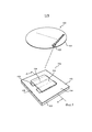
Фиг.1 схематически иллюстрирует перспективное изображение устройства светового выхода согласно одному варианту осуществления данного изобретения;1 schematically illustrates a perspective view of a light output device according to one embodiment of the present invention;
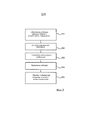
Фиг.2 является блок-схемой, схематически иллюстрирующей один вариант осуществления способа обеспечения отражающего покрытия для подложки согласно данному изобретению;FIG. 2 is a flowchart schematically illustrating one embodiment of a method for providing a reflective coating for a substrate according to this invention;
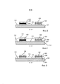
Фиг.3 схематически иллюстрирует один вариант осуществления подложки, имеющей контактные площадки, расположенные на ней;Figure 3 schematically illustrates one embodiment of a substrate having contact pads located thereon;
Фиг.4 схематически иллюстрирует вариант фиг.3, имеющий отражающее соединение, нанесенное на подложку; иFigure 4 schematically illustrates a variant of figure 3, having a reflective compound deposited on a substrate; and
Фиг.5 схематически иллюстрирует вариант фиг.4, причем отражающее покрытие было удалено с контактных площадок.Figure 5 schematically illustrates a variant of figure 4, and the reflective coating has been removed from the pads.
ОПИСАНИЕ ПРИМЕРНЫХ ВАРИАНТОВ ОСУЩЕСТВЛЕНИЯ ДАННОГО ИЗОБРЕТЕНИЯDESCRIPTION OF EXEMPLARY EMBODIMENTS FOR CARRYING OUT THE INVENTION
В нижеследующем описании данное изобретение описывается со ссылкой на способ обеспечения отражающего покрытия на керамическую подложку для светоизлучающего устройства. Отражающее соединение обеспечено на верхней части подложки, имеющей металлические контактные площадки для электрического соединения со светоизлучающим устройством. Это отражающее соединение подвергается процессу отверждения и после этого удаляется из контактных площадок подложки. Нижеследующее будет также описывать подложку, обеспечиваемую этим способом.In the following description, the invention is described with reference to a method of providing a reflective coating on a ceramic substrate for a light-emitting device. A reflective connection is provided on the upper part of the substrate having metal pads for electrical connection with the light emitting device. This reflective compound undergoes a curing process and is then removed from the contact pads of the substrate. The following will also describe the substrate provided by this method.
Следует отметить, что это описание подложки никоим образом не ограничивает объем данного изобретения, которое равным образом применимо с другими материалами подложки, такими как нитрид алюминия, кремний, алюминий и т.д. В случае металлической подложки, такой как алюминий, может быть образован слой диэлектрика между подложкой и металлическими дорожками для электрического экранирования металлических электродов от проводящей подложки. Кроме того, металлические контактные площадки и металлические дорожки не должны быть обязательно скомпонованы из трех слоев различных металлических материалов; это изобретение равным образом применимо только с единственным или двойным слоем материала или может включать в себя даже большее количество слоев.It should be noted that this description of the substrate in no way limits the scope of the present invention, which is equally applicable to other substrate materials, such as aluminum nitride, silicon, aluminum, etc. In the case of a metal substrate, such as aluminum, a dielectric layer may be formed between the substrate and the metal tracks to electrically shield the metal electrodes from the conductive substrate. In addition, metal pads and metal tracks do not need to be composed of three layers of different metal materials; this invention is equally applicable only with a single or double layer of material or may include even more layers.
Фиг.1 схематически иллюстрирует слоистый (вафельный) материал 100, содержащий множество светоизлучающих устройств 102, причем каждое устройство 102 светового выхода имеет подложку 104, металлические контактные площадки 106 и металлические дорожки 108. Этот слоистый материал может быть в виде квадрата, но может также находиться в других формах, таких как прямоугольная или круглая форма. Более конкретно, каждое устройство 102 светового выхода содержит подложку 104, имеющую на ее верхней поверхности 110 металлические контактные площадки 106 и металлические дорожки 108 для электрического возбуждения светоизлучающего устройства 112, которое помещено на металлические контактные площадки 106 этой подложки. Зона/пространство между светоизлучающим устройством 112 и верхней поверхностью 110 может быть заполнена материалом наполнителя для поддержки устройства 112. Этот наполнитель может быть отражающим покрытием 114 или покрывать отражающее покрытие 114. Подложка 104 в описываемом варианте осуществления состоит из керамического материала, такого как оксид алюминия, Al2O3. Подложка 104 имеет желаемую теплопроводность и, следовательно, может действовать в качестве распространителя тепла для отведения тепла, генерируемого светоизлучающим устройством (обычно одного или нескольких светоизлучающих диодов - СИД). Кроме того, на первой части 16 поверхности подложки 104, которая не обеспечена металлическими контактными площадками 106 и металлическими дорожками 108, не обеспечена отражающим покрытием 114, которое помещено для отражения света, излучаемого светоизлучающим устройством 112 на ней. Кроме того, отражающее покрытие 114 содержит в иллюстрированном варианте осуществления пигменты, связывающий материал и дополнительные наполнители. Пигменты помещены для обеспечения желаемой отражающей характеристики этого покрытия и в иллюстрированном варианте осуществления являются материалом диоксида титана, имеющим распределение размеров частиц в диапазоне между 100-1000 нм. Пигмент вызывает рассеяние в покрытии. Посредством оптимизации количества пигмента относительно связующего материала и отбора пигментов и связующих материалов с большими различиями показателя преломления может быть получено высокорассеянное, следовательно, отражающее покрытие при применении подходящей толщины покрытия. Величина отражательной способности может быть настроена. Обычно желательно достижение высокой отражательной способности, например достижение отражательной способности, более высокой чем 80%, предпочтительно более высокой чем 90%, более предпочтительно более высокой чем 95%. Обычная толщина слоя для отражающего покрытия находится в диапазоне от приблизительно 1 микрона до приблизительно 10 микронов. Более толстый слой обычно приводит к более высокой отражательной способности. Связующий материал отражающего соединения помещают для обеспечения химической связи между покрытием 114 и первой частью 116 поверхности, так что покрытие 114 прикрепляется к первой части 116 поверхности желаемым образом. Связующий материал в иллюстрированном варианте осуществления предпочтительно является золь-гель-связующим материалом, полученным из мономера силана. Эти мономеры по меньшей мере частично гидролизуют перед обеспечением этой подложки. Типичные мономеры силана могут быть, например, метилтриметоксисиланом, метилтриэтоксисиланом, фенилтриметоксисиланом или алкилалкоксисиланами и т.д. Дополнительно также типичный дополнительный наполнитель может быть частицами диоксида кремния, частицами оксида алюминия или частицами диоксида титана с размером приблизительно 5-100 нм, которые помещают для усадки (сморщивания) покрытия 114 в фазе отверждения, которое будет дополнительно описано ниже в связи со способом обеспечения нанесения покрытия на подложку 104.1 schematically illustrates a laminate (waffle)
Примерный вариант осуществления способа согласно данному изобретению для обеспечения отражающего покрытия на подложке будет теперь описан со ссылкой на фиг 2, иллюстрирующей блок-схему этого способа. Следует отметить, что этот способ описан без светоизлучающего устройства 112, помещенного на металлические контактные площадки 106. Однако это не должно интерпретироваться как ограничение объема этой заявки, которая может быть также применима в светоизлучающем устройстве 112, помещенном на металлические контактные площадки 106 в связи с первой стадией 201 этого способа.An exemplary embodiment of the method according to this invention for providing a reflective coating on a substrate will now be described with reference to FIG. 2, illustrating a flow diagram of this method. It should be noted that this method is described without a
Согласно стадии 201 этого способа металлические контактные площадки 106 и металлические дорожки 108 размещены на верхней поверхности 110 подложки 104, которая подробно иллюстрируется на фиг.3. Кроме того, металлические контактные площадки 106 и металлические дорожки 108 в иллюстрированном варианте осуществления монтируются посредством слоя 201 меди, покрытой слоем 202 никеля и слоем 203 золота, причем слой 203 золота обеспечен на верхней поверхности 110 металлических контактных площадок 106 и металлических дорожек 108 для электрического возбуждения светоизлучающего устройства 112, расположенного на ней, как иллюстрировано на фиг.1. Альтернативно, слой золота может также покрывать медь соответствующим образом, с покрыванием, следовательно, также и боковых граней металлических контактных площадок 106 и металлических дорожек 108.According to step 201 of this method,
Теперь ссылка на вторую стадию 202 этого способа также иллюстрируется на фиг.4. Отражающее соединение 401 обеспечено на верхней поверхности 110 подложки 104, включающей в себя металлические контактные площадки 106 и металлические дорожки 108. Отражающее соединение 401 может быть обеспечено, например, посредством распыленного покрытия подложки 104 при заданной скорости в иллюстрированном варианте осуществления, например, со скоростью 10 мм/с. Подложка 104, металлические контактные площадки 106 и металлические дорожки 108, таким образом, после второй стадии 202 по меньшей мере частично покрыты отражающим соединением 401. Отражающее соединение содержит пигменты, связующий материал и дополнительный наполнитель, как описано в отношении фиг.1. Также отражающее соединение 401 дополнительно содержит растворитель, например воду или другие растворители, такие как этанол, изопропанол или бутанол. Напыленный слой может быть применен на всей площади подложки, но может также применяться только на части площади подложки. После нанесения покрытия подложку сушат для удаления по меньшей мере части этих растворителей.Now, reference to the
После этого на третьей стадии 203 отражающее соединение 401 по меньшей мере частично отверждают при заданной температуре во время заданного времени, с образованием отражающего покрытия 114 на подложке 104, металлических контактных площадок 106 и металлических дорожек 108. Это по меньшей мере частичное отверждение является в иллюстрированном варианте осуществления тепловым процессом, причем соединение 401 нагревают в течение 30 минут при температуре приблизительно 80°С. При подвергании фазе отверждения силановые мономеры или форполимеры золь-гель-связующего материала будут реагировать с силикатной сеткой или алкилсиликатной сеткой с образованием сшивания этого связующего материала. Предпочтительно золь-гель-связующий материал образует метилсиликатную сетку, которая может слипаться желаемым образом с керамической подложкой первой части 116 поверхности подложки, но может слипаться меньше с верхней поверхностью 203 металлических контактных площадок 106 и металлических дорожек 108. Это осуществляется, так как образуется химическая связь между золь-гель-связующим материалом и подложкой из оксида алюминия. Однако различие в шероховатости поверхности может также обеспечить лучшее прилипание отражающего покрытия к отражающей подложке, чем к металлическим контактным площадкам 106 и металлическим дорожкам 108. Например, керамическая подложка может быть относительно неровной для обеспечения зоны для захвата отражающего покрытия, в то время как металлические контактные площадки 106 и металлические дорожки 108 имеют менее шероховатую поверхность. Кроме того, золь-гель-связующий материал может быть выполнен таким образом, что он прикрепляется также желаемым образом к материалам из меди 201 и никеля 202 металлических контактных площадок 106 и металлических дорожек 108. Дополнительно, согласно одному варианту осуществления данного изобретения отражающее покрытие 114 может иметь состав, содержащий между 10-60 об.% пигментов и остальную часть, образованную этим связующим материалом. Необязательно, может присутствовать дополнительный наполнитель, например, в количестве 0-30 об.%. Например, этот состав может быть 20 об.% наноSiO2, 30 об.% метилсиликатным связующим материалом и 50 об.% TiO2. Это покрытие может также включать в себя поры, не представленные в вышеупомянутых объемных процентах, которые могут также способствовать рассеянию. Кроме того, если желательным является увеличение толщины отражающего покрытия 114, например, для повышения отражающей способности или однородности поверхности или ровности (плоскостности) поверхности, первая стадия 201, вторая стадия 202 и третья стадия 203 могут повторяться, пока не будет нанесено удовлетворительное количество отражающего покрытия 114 на подложку 104.Thereafter, in the
После отверждения этого соединения, т.е. после стадии 203 этого способа, подложку подвергают фазе пропитывания, т.е. четвертой стадии 204 фиг.2. Таким образом, подложку 104 подвергают действию растворителя, например воды и/или ацетона, которые могут дополнительно уменьшать связь между отражающим покрытием 114 и металлическими контактными площадками 106 и металлическими дорожками 108. Этот растворитель может содержать травитель для металлических площадок, например кислоту, для облегчения высвобождения покрытия.After curing this compound, i.e. after
Теперь со ссылкой на фиг.5 иллюстрируется пятая стадия 205 этого способа, т.е. удаление отражающего покрытия 114 из металлических контактных площадок 106 и металлических дорожек 108. На этой стадии подложку 104 подвергают механической обработке, такой как давление распыления жидкости, которая удаляет отражающее покрытие 114 из металлических контактных площадок 106, а также из металлических дорожек 108. Однако вследствие химической связи между золь-гель-связующим материалом отражающего покрытия 114 и керамической подложки 104, как описано выше, отражающее покрытие 114 не удаляется из керамической подложки 104 при подвергании этой механической обработке. Таким образом, как показано на фиг.5, керамическая подложка 104 покрывается отражающим покрытием 114, в то время как металлические контактные площадки 106 и металлические дорожки 108 имеют «чистую» поверхность без обеспечения желаемого электрического соединения со светоизлучающим устройством 112, связанным с ней.Now, with reference to FIG. 5, the
Согласно одному варианту осуществления данного изобретения и для дополнительного увеличения отражающей способности подложки 110 металлические дорожки 108 могут быть также обеспечены отражающим покрытием 114 после пятой стадии 205 этого способа. В таком случае по меньшей мере часть металлических дорожек 108, которые не должны находиться в соединении со светоизлучающим устройством 112 после сборки, могут быть обеспечены усилителем адгезии перед нанесением отражающего соединения 401, как иллюстрировано во второй стадии 202 этого способа, а также на фиг.4. Способом достижения этого является предварительное структурирование подложки со структурой, выполняемой в слое фоторезиста. Слой фоторезиста покрывает зоны, которые не должны быть покрыты усиливающим адгезию слоем. Затем наносят усиливающий адгезию слой, например, погружением подложки в баню, содержащую усилитель адгезии, растворенный в растворителе. Этим усилителем адгезии может быть, например, 3-меркаптопропилтриметоксисилан, из которого меркаптогруппа реагирует, например, с золотом, и метоксигруппы могут быть химически связаны с силикатной или алкилсиликатной сеткой. Таким образом, химическая связь между металлическими дорожками 108 и отражающим покрытием 114 может быть увеличена для поддержания четвертой стадии 204 и пятой стадии 205, описанных выше, таким же образом, что и первая часть поверхности 116.According to one embodiment of the present invention, and to further increase the reflectivity of the
Дополнительно, из исследования чертежей, описания и прилагаемой формулы изобретения квалифицированному специалисту, выполняющему на практике заявленное изобретение, могут быть понятны, и им могут быть выполнены вариации описанных вариантов осуществления. Например, пигмент, используемый в отражающем покрытии, может быть вместо диоксида титана либо типа рутила TiO2, либо типа анатаза TiO2, одним из оксида алюминия, диоксида циркония, оксида гафния, оксида иттрия или оксида тантала, титаната бария, титаната стронция или смесью таких пигментов и т.д. Кроме того, усилитель адгезии, наносимый на металлические дорожки, может дополнительно включать в себя, например, процедуру погружения или процедуру стриппинга. Дополнительно также механическая обработка удаления отражающего покрытия из металлических контактных площадок может также содержать измельчение, дробление, впрыскивание струи или ультразвуковую обработку, мегазвуковую обработку и т.д. Для дополнительного облегчения удаления покрытия из металлических дорожек эта поверхность может быть предварительно обработана разделительным слоем. Этот разделительный слой может быть удален после высвобождения покрытия для достижения надежной контактной зоны для светоизлучающего устройства. Этот разделительный слой может быть тонким слоем, таким как самособираемый монослой функционализированных тиолов. Известно, что тиоловые группы прилипают к золоту, эта функциональная группа может обеспечивать свойства неприлипания. Разделительный слой может быть удален после этого, например, обработкой кислородной плазмой. Разделительный слой может быть также подходящим слоем фоторезиста, или другие разделительные слои могут быть обеспечены на металлических дорожках.Additionally, from a study of the drawings, description and appended claims, a qualified professional practicing the claimed invention may be understood, and variations of the described embodiments may be made to them. For example, the pigment used in the reflective coating may be, instead of titanium dioxide, either rutile type TiO 2 or anatase TiO 2 , one of alumina, zirconia, hafnium oxide, yttrium oxide or tantalum oxide, barium titanate, strontium titanate, or a mixture such pigments, etc. In addition, the adhesion promoter applied to the metal tracks may further include, for example, a dipping procedure or a stripping procedure. Additionally, the machining of the removal of the reflective coating from the metal pads may also include grinding, crushing, injection of the jet or ultrasonic treatment, megasonic processing, etc. To further facilitate removal of the coating from metal tracks, this surface can be pre-treated with a separation layer. This separation layer can be removed after release of the coating to achieve a reliable contact area for the light emitting device. This separation layer may be a thin layer, such as a self-assembled monolayer of functionalized thiols. Thiol groups are known to adhere to gold; this functional group can provide non-adherence properties. The separation layer may then be removed, for example, by treatment with oxygen plasma. The separation layer may also be a suitable photoresist layer, or other separation layers may be provided on the metal tracks.
Кроме того, композиция материала отражающего покрытия может иметь состав, содержащий вариацию из: 10-90 об.% отвержденного золь-гель-материала, 10-60 об.% пигментного наполнителя диоксида титана и 0-40 об.% наполнителя нанодиоксида кремния. Более предпочтительно, этот состав представляет собой 20-50 об.% связующего материала, 30-50 об.% пигмента и 10-20 об. % нанонаполнителя.In addition, the composition of the material of the reflective coating may have a composition containing a variation of: 10-90 vol.% Cured sol-gel material, 10-60 vol.% Pigment filler of titanium dioxide and 0-40 vol.% Filler of silicon dioxide. More preferably, this composition is 20-50 vol.% Binder, 30-50 vol.% Pigment and 10-20 vol. % nanofiller.
Кроме того, структура фоторезиста может покрывать металлические дорожки и металлические контактные площадки в зонах, которые не должны быть покрыты отражающим покрытием. Затем зоны, которые не должны быть покрыты отражающим покрытием, могут быть обработаны высвобождающим слоем, который уменьшает адгезию. После удаления фоторезиста выполняют процесс нанесения покрытия, приводящий к высвобождению покрытия только из предварительно структурированного разделительного слоя. Дополнительно, носитель подложки может быть также печатной платой или ламинатом, например многослойной печатной платой. Таким образом, этот носитель может состоять из множественных слоев, и поверхность подложки не должна обязательно состоять только из одного типа материала, но может быть также покрыта различными материалами.In addition, the photoresist structure can cover metal tracks and metal pads in areas that should not be covered with a reflective coating. Then areas that should not be coated with a reflective coating can be treated with a release layer that reduces adhesion. After removal of the photoresist, a coating process is performed leading to the release of the coating only from the pre-structured separation layer. Additionally, the substrate carrier may also be a printed circuit board or a laminate, for example a multilayer printed circuit board. Thus, this carrier can consist of multiple layers, and the surface of the substrate does not have to consist of only one type of material, but can also be coated with various materials.
Кроме того, другие вещества, чем вода и ацетон, могут быть использованы в фазе пропитывания для обеспечения упрощенного удаления отражающего покрытия, например метилацетата, этилацетата, бутилацетата, этанола, изопропанола или других спиртов и т.д.In addition, other substances than water and acetone can be used in the impregnation phase to provide simplified removal of the reflective coating, for example methyl acetate, ethyl acetate, butyl acetate, ethanol, isopropanol or other alcohols, etc.
В формуле изобретения слово «содержащий» не исключает других элементов или стадий, и указание на единственность не исключает множественности. Единственный процессор или другой узел может выполнять функции нескольких элементов, цитируемых в формуле изобретения. Сам факт, что некоторые меры излагаются во взаимно различных зависимых пунктов, не указывает на то, что комбинации этих мер не могут быть выгодно использованы.In the claims, the word “comprising” does not exclude other elements or stages, and an indication of uniqueness does not exclude plurality. A single processor or other node may fulfill the functions of several elements cited in the claims. The fact that some measures are stated in mutually different dependent clauses does not indicate that combinations of these measures cannot be used to advantage.
Claims (14)
обеспечения подложки, имеющей первую часть поверхности с первым материалом поверхности и вторую часть поверхности со вторым материалом поверхности, отличающимся от первого материала поверхности;
нанесения отражающего соединения на указанный первый материал поверхности и указанный второй материал поверхности для образования связи с подложкой в первой части поверхности, которая является более сильной, чем связь между отражающим соединением и подложкой во второй части поверхности;
по меньшей мере частичного отверждения указанного отражающего соединения для образования отражающего покрытия, на первой части поверхности и второй части поверхности; и
подвергания указанного отражающего покрытия на первой и второй частях поверхности механической обработке, которая преодолевает связь с подложкой во второй части поверхности, чтобы таким образом удалить указанное отражающее покрытие по меньшей мере из части указанной второй части поверхности, в то время как указанное отражающее покрытие остается на указанной первой части поверхности.1. A method of manufacturing a structure comprising a reflective coating on a substrate for a light-emitting device, the method comprises the steps of:
providing a substrate having a first surface part with a first surface material and a second surface part with a second surface material different from the first surface material;
applying a reflective compound to said first surface material and said second surface material to form a bond with the substrate in the first part of the surface, which is stronger than the bond between the reflective compound and the substrate in the second part of the surface;
at least partially curing said reflective compound to form a reflective coating on a first surface part and a second surface part; and
subjecting said reflective coating on the first and second parts of the surface to machining, which overcomes the bond with the substrate in the second surface, so as to remove said reflective coating from at least a portion of said second surface, while said reflective coating remains on said the first part of the surface.
Applications Claiming Priority (3)
| Application Number | Priority Date | Filing Date | Title |
|---|---|---|---|
| EP11158839.8 | 2011-03-18 | ||
| EP11158839A EP2500623A1 (en) | 2011-03-18 | 2011-03-18 | Method for providing a reflective coating to a substrate for a light-emitting device |
| PCT/IB2012/051112 WO2012127349A1 (en) | 2011-03-18 | 2012-03-09 | Method for providing a reflective coating to a substrate for a light-emitting device |
Publications (2)
| Publication Number | Publication Date |
|---|---|
| RU2013146546A RU2013146546A (en) | 2015-04-27 |
| RU2597253C2 true RU2597253C2 (en) | 2016-09-10 |
Family
ID=44317608
Family Applications (1)
| Application Number | Title | Priority Date | Filing Date |
|---|---|---|---|
| RU2013146546/07A RU2597253C2 (en) | 2011-03-18 | 2012-03-09 | Method of providing reflecting coating for substrate for light-emitting device |
Country Status (9)
| Country | Link |
|---|---|
| US (2) | US9660147B2 (en) |
| EP (2) | EP2500623A1 (en) |
| JP (1) | JP2014509086A (en) |
| KR (1) | KR101934891B1 (en) |
| CN (1) | CN103429949B (en) |
| BR (1) | BR112013023558B1 (en) |
| RU (1) | RU2597253C2 (en) |
| TW (1) | TWI560907B (en) |
| WO (1) | WO2012127349A1 (en) |
Families Citing this family (12)
| Publication number | Priority date | Publication date | Assignee | Title |
|---|---|---|---|---|
| US9293667B2 (en) | 2010-08-19 | 2016-03-22 | Soraa, Inc. | System and method for selected pump LEDs with multiple phosphors |
| KR101304715B1 (en) * | 2012-04-25 | 2013-09-06 | 주식회사 엘지씨엔에스 | Method and apparatus for preventing light leakagein a light guide plate and display device having a light guide plate painted with reflect ink |
| WO2014103326A1 (en) * | 2012-12-27 | 2014-07-03 | コニカミノルタ株式会社 | Coating liquid, and led device provided with reflective layer that is formed of cured product of said coating liquid |
| WO2015092579A1 (en) * | 2013-12-18 | 2015-06-25 | Koninklijke Philips N.V. | Reflective solder mask layer for led phosphor package |
| US20160020370A1 (en) * | 2014-07-21 | 2016-01-21 | GE Lighting Solutions, LLC | Thin film with multilayer dielectric coatings for light emitting diode (led) lead frame and chip-on-board (cob) substrate reflector |
| TWI647191B (en) | 2015-06-11 | 2019-01-11 | 美商蘋果公司 | Transparent protective coatings for a component of an electronic device |
| EP3351062A1 (en) * | 2015-09-15 | 2018-07-25 | Philips Lighting Holding B.V. | Barrier layer delaying oxygen depletion in sealed gas-filled led lamps |
| WO2017142888A1 (en) * | 2016-02-18 | 2017-08-24 | 3M Innovative Properties Company | Multilayer construction for mounting light emitting devices |
| US11098218B2 (en) | 2018-09-26 | 2021-08-24 | Apple Inc. | Coatings for electronic devices |
| DE102018129575A1 (en) * | 2018-11-23 | 2020-05-28 | Osram Opto Semiconductors Gmbh | Light emitter unit with at least one VCSEL chip |
| US11837684B2 (en) * | 2019-11-21 | 2023-12-05 | Creeled, Inc. | Submount structures for light emitting diode packages |
| US11873954B2 (en) * | 2020-09-03 | 2024-01-16 | Signify Holding B.V. | Lighting board and luminaire using the lighting board |
Citations (6)
| Publication number | Priority date | Publication date | Assignee | Title |
|---|---|---|---|---|
| US6845184B1 (en) * | 1998-10-09 | 2005-01-18 | Fujitsu Limited | Multi-layer opto-electronic substrates with electrical and optical interconnections and methods for making |
| US20060012991A1 (en) * | 2004-07-15 | 2006-01-19 | Gelcore, Llc | Led lighting system with reflective board |
| WO2009075530A2 (en) * | 2007-12-13 | 2009-06-18 | Amoleds Co., Ltd. | Semiconductor and manufacturing method thereof |
| EP2216834A1 (en) * | 2007-11-29 | 2010-08-11 | Nichia Corporation | Light-emitting device and its manufacturing method |
| EP2228841A1 (en) * | 2009-03-09 | 2010-09-15 | Ledon Lighting Jennersdorf GmbH | LED module with improved light output |
| US20110049545A1 (en) * | 2009-09-02 | 2011-03-03 | Koninklijke Philips Electronics N.V. | Led package with phosphor plate and reflective substrate |
Family Cites Families (19)
| Publication number | Priority date | Publication date | Assignee | Title |
|---|---|---|---|---|
| US4662927A (en) | 1985-12-17 | 1987-05-05 | Emhart Industries, Inc. | Glass temperature preconditioning system in a distribution channel |
| US6885147B2 (en) * | 1998-05-18 | 2005-04-26 | Emagin Corporation | Organic light emitting diode devices with improved anode stability |
| US20030236318A1 (en) | 2002-04-18 | 2003-12-25 | Kuraray Co., Ltd. | Curable resin composition, method for manufacture of laminate using the composition, transfer material, method for manufacture thereof and transferred product |
| JP4179866B2 (en) * | 2002-12-24 | 2008-11-12 | 株式会社沖データ | Semiconductor composite device and LED head |
| US7285802B2 (en) | 2004-12-21 | 2007-10-23 | 3M Innovative Properties Company | Illumination assembly and method of making same |
| JP2007042668A (en) | 2005-07-29 | 2007-02-15 | Toyoda Gosei Co Ltd | Led light emitting device |
| JP2007281260A (en) * | 2006-04-07 | 2007-10-25 | Sumitomo Metal Electronics Devices Inc | Reflector, package for housing light-emitting element using the same, and lens used for reflector |
| US20090032829A1 (en) * | 2007-07-30 | 2009-02-05 | Tong Fatt Chew | LED Light Source with Increased Thermal Conductivity |
| TWI360238B (en) | 2007-10-29 | 2012-03-11 | Epistar Corp | Photoelectric device |
| KR100979174B1 (en) | 2008-06-05 | 2010-08-31 | (주) 아모엘이디 | Multi-chip package and manufacturing method thereof |
| JP5355219B2 (en) | 2008-05-21 | 2013-11-27 | 京セラ株式会社 | Light emitting element mounting substrate and light emitting device |
| US20100279437A1 (en) | 2009-05-01 | 2010-11-04 | Koninklijke Philips Electronics N.V. | Controlling edge emission in package-free led die |
| EP2335295B1 (en) | 2008-09-25 | 2021-01-20 | Lumileds LLC | Coated light emitting device and method of coating thereof |
| JP5665285B2 (en) | 2009-06-15 | 2015-02-04 | 日立化成株式会社 | Optical semiconductor element mounting member and optical semiconductor device |
| US8704258B2 (en) | 2009-06-26 | 2014-04-22 | Asahi Rubber Inc. | White color reflecting material and process for production thereof |
| US8431423B2 (en) | 2009-07-16 | 2013-04-30 | Koninklijke Philips Electronics N.V. | Reflective substrate for LEDS |
| US8486761B2 (en) * | 2010-03-25 | 2013-07-16 | Koninklijke Philips Electronics N.V. | Hybrid combination of substrate and carrier mounted light emitting devices |
| WO2012002580A1 (en) * | 2010-07-01 | 2012-01-05 | シチズンホールディングス株式会社 | Led light source device and method for manufacturing same |
| JP2012151191A (en) * | 2011-01-17 | 2012-08-09 | Ibiden Co Ltd | Wiring board for led, light emitting module, manufacturing method of the wiring board for the led, and manufacturing method of the light emitting module |
-
2011
- 2011-03-18 EP EP11158839A patent/EP2500623A1/en not_active Withdrawn
-
2012
- 2012-03-09 RU RU2013146546/07A patent/RU2597253C2/en active
- 2012-03-09 US US14/002,202 patent/US9660147B2/en active Active
- 2012-03-09 CN CN201280014057.6A patent/CN103429949B/en active Active
- 2012-03-09 WO PCT/IB2012/051112 patent/WO2012127349A1/en active Application Filing
- 2012-03-09 BR BR112013023558-6A patent/BR112013023558B1/en active IP Right Grant
- 2012-03-09 KR KR1020137027446A patent/KR101934891B1/en active IP Right Grant
- 2012-03-09 JP JP2013558543A patent/JP2014509086A/en active Pending
- 2012-03-09 EP EP12710357.0A patent/EP2686604B8/en active Active
- 2012-03-15 TW TW101108935A patent/TWI560907B/en active
-
2017
- 2017-05-03 US US15/586,120 patent/US10043959B2/en active Active
Patent Citations (6)
| Publication number | Priority date | Publication date | Assignee | Title |
|---|---|---|---|---|
| US6845184B1 (en) * | 1998-10-09 | 2005-01-18 | Fujitsu Limited | Multi-layer opto-electronic substrates with electrical and optical interconnections and methods for making |
| US20060012991A1 (en) * | 2004-07-15 | 2006-01-19 | Gelcore, Llc | Led lighting system with reflective board |
| EP2216834A1 (en) * | 2007-11-29 | 2010-08-11 | Nichia Corporation | Light-emitting device and its manufacturing method |
| WO2009075530A2 (en) * | 2007-12-13 | 2009-06-18 | Amoleds Co., Ltd. | Semiconductor and manufacturing method thereof |
| EP2228841A1 (en) * | 2009-03-09 | 2010-09-15 | Ledon Lighting Jennersdorf GmbH | LED module with improved light output |
| US20110049545A1 (en) * | 2009-09-02 | 2011-03-03 | Koninklijke Philips Electronics N.V. | Led package with phosphor plate and reflective substrate |
Also Published As
| Publication number | Publication date |
|---|---|
| US20140001497A1 (en) | 2014-01-02 |
| US10043959B2 (en) | 2018-08-07 |
| CN103429949A (en) | 2013-12-04 |
| US20170236987A1 (en) | 2017-08-17 |
| BR112013023558A2 (en) | 2016-12-06 |
| BR112013023558B1 (en) | 2021-05-25 |
| JP2014509086A (en) | 2014-04-10 |
| EP2500623A1 (en) | 2012-09-19 |
| EP2686604B8 (en) | 2018-08-29 |
| US9660147B2 (en) | 2017-05-23 |
| KR20140013033A (en) | 2014-02-04 |
| EP2686604A1 (en) | 2014-01-22 |
| TWI560907B (en) | 2016-12-01 |
| EP2686604B1 (en) | 2018-02-21 |
| CN103429949B (en) | 2017-07-07 |
| WO2012127349A1 (en) | 2012-09-27 |
| TW201244175A (en) | 2012-11-01 |
| KR101934891B1 (en) | 2019-01-04 |
| RU2013146546A (en) | 2015-04-27 |
Similar Documents
| Publication | Publication Date | Title |
|---|---|---|
| RU2597253C2 (en) | Method of providing reflecting coating for substrate for light-emitting device | |
| JP5628425B2 (en) | Semiconductor component and method for manufacturing semiconductor component | |
| TWI468087B (en) | Led wiring board, light emitting module, method for manufacturing led wiring board and method for manufacturing light emitting module | |
| KR101923738B1 (en) | Light emitting device and method for manufacturing the same | |
| KR102131747B1 (en) | Led with ceramic green phosphor and protected red phosphor layer | |
| TWI407581B (en) | Color converted light emitting diode | |
| TWI473293B (en) | Fabrication of compact opto-electronic component packages | |
| JP6383818B2 (en) | Patterned UV-sensitive silicone-phosphor layer on LED | |
| US20140036461A1 (en) | Flexible led device for thermal management and method of making | |
| EP2628194B1 (en) | Method of manufacturing a light emitting device | |
| KR20130110101A (en) | Inorganic shaped body for converting wavelength and method for manufacturing the same, and light emitting device | |
| WO2012141692A2 (en) | Method for transferring a uniform phosphor layer on an article and light-emitting structure fabricated by the method | |
| US20160155891A1 (en) | Optoelectronic component and method for the production thereof | |
| TW201724580A (en) | Package, light-emitting device, and methods of manufacturing the package and light-emitting device | |
| TW201242072A (en) | Light emitting semiconductor device having multi-level substrate | |
| US10121951B2 (en) | Light-emitting device substrate, light-emitting device, and method for producing light-emitting device substrate | |
| JPS59154034A (en) | Semiconductor device |
Legal Events
| Date | Code | Title | Description |
|---|---|---|---|
| PC41 | Official registration of the transfer of exclusive right |
Effective date: 20190823 |
|
| PD4A | Correction of name of patent owner |