RU2573447C2 - Capacitance measurement system - Google Patents
Capacitance measurement system Download PDFInfo
- Publication number
- RU2573447C2 RU2573447C2 RU2012132637/28A RU2012132637A RU2573447C2 RU 2573447 C2 RU2573447 C2 RU 2573447C2 RU 2012132637/28 A RU2012132637/28 A RU 2012132637/28A RU 2012132637 A RU2012132637 A RU 2012132637A RU 2573447 C2 RU2573447 C2 RU 2573447C2
- Authority
- RU
- Russia
- Prior art keywords
- sensor
- sensors
- electrode
- electrodes
- measuring
- Prior art date
Links
- 238000005259 measurement Methods 0.000 title claims abstract description 78
- 239000010409 thin film Substances 0.000 claims abstract description 41
- 239000010408 film Substances 0.000 claims abstract description 28
- 230000002093 peripheral effect Effects 0.000 claims abstract description 16
- 238000012545 processing Methods 0.000 claims description 56
- 239000012528 membrane Substances 0.000 claims description 7
- 229920003223 poly(pyromellitimide-1,4-diphenyl ether) Polymers 0.000 claims description 7
- 238000012216 screening Methods 0.000 claims description 5
- 239000010410 layer Substances 0.000 abstract description 117
- 238000004519 manufacturing process Methods 0.000 abstract description 16
- 230000000694 effects Effects 0.000 abstract description 12
- 239000011241 protective layer Substances 0.000 abstract description 8
- 239000000126 substance Substances 0.000 abstract 1
- 239000004065 semiconductor Substances 0.000 description 168
- 235000012431 wafers Nutrition 0.000 description 157
- 239000000758 substrate Substances 0.000 description 62
- 238000013461 design Methods 0.000 description 41
- 238000000034 method Methods 0.000 description 31
- 238000010586 diagram Methods 0.000 description 29
- 239000000523 sample Substances 0.000 description 24
- 230000005684 electric field Effects 0.000 description 20
- 230000010363 phase shift Effects 0.000 description 18
- 239000000463 material Substances 0.000 description 16
- 230000006870 function Effects 0.000 description 14
- 230000001360 synchronised effect Effects 0.000 description 14
- 230000008859 change Effects 0.000 description 13
- 239000004020 conductor Substances 0.000 description 13
- XUIMIQQOPSSXEZ-UHFFFAOYSA-N Silicon Chemical compound [Si] XUIMIQQOPSSXEZ-UHFFFAOYSA-N 0.000 description 11
- 229910052710 silicon Inorganic materials 0.000 description 11
- 239000010703 silicon Substances 0.000 description 11
- RZVAJINKPMORJF-UHFFFAOYSA-N Acetaminophen Chemical compound CC(=O)NC1=CC=C(O)C=C1 RZVAJINKPMORJF-UHFFFAOYSA-N 0.000 description 10
- 239000002245 particle Substances 0.000 description 10
- 239000005297 pyrex Substances 0.000 description 10
- 230000035945 sensitivity Effects 0.000 description 9
- RYGMFSIKBFXOCR-UHFFFAOYSA-N Copper Chemical compound [Cu] RYGMFSIKBFXOCR-UHFFFAOYSA-N 0.000 description 8
- 229910052802 copper Inorganic materials 0.000 description 8
- 239000010949 copper Substances 0.000 description 8
- 230000003071 parasitic effect Effects 0.000 description 8
- 238000012937 correction Methods 0.000 description 7
- 230000003287 optical effect Effects 0.000 description 7
- 230000008901 benefit Effects 0.000 description 6
- 239000003292 glue Substances 0.000 description 6
- 239000011159 matrix material Substances 0.000 description 6
- 238000007781 pre-processing Methods 0.000 description 6
- 238000007639 printing Methods 0.000 description 6
- 239000003990 capacitor Substances 0.000 description 5
- 238000010276 construction Methods 0.000 description 5
- 230000008878 coupling Effects 0.000 description 5
- 238000010168 coupling process Methods 0.000 description 5
- 238000005859 coupling reaction Methods 0.000 description 5
- 238000006073 displacement reaction Methods 0.000 description 5
- 230000005284 excitation Effects 0.000 description 5
- 238000009434 installation Methods 0.000 description 5
- 239000011229 interlayer Substances 0.000 description 5
- 230000008569 process Effects 0.000 description 5
- 239000000853 adhesive Substances 0.000 description 4
- 230000001070 adhesive effect Effects 0.000 description 4
- 230000015572 biosynthetic process Effects 0.000 description 4
- 238000010894 electron beam technology Methods 0.000 description 4
- 238000005516 engineering process Methods 0.000 description 4
- 230000001747 exhibiting effect Effects 0.000 description 4
- 239000011810 insulating material Substances 0.000 description 4
- 229920001721 polyimide Polymers 0.000 description 4
- 230000001681 protective effect Effects 0.000 description 4
- 230000007704 transition Effects 0.000 description 4
- 238000004026 adhesive bonding Methods 0.000 description 3
- 239000011248 coating agent Substances 0.000 description 3
- 238000000576 coating method Methods 0.000 description 3
- 230000000052 comparative effect Effects 0.000 description 3
- 238000005530 etching Methods 0.000 description 3
- 230000005855 radiation Effects 0.000 description 3
- 238000012546 transfer Methods 0.000 description 3
- 238000004364 calculation method Methods 0.000 description 2
- 150000001875 compounds Chemical class 0.000 description 2
- 239000000356 contaminant Substances 0.000 description 2
- 230000017525 heat dissipation Effects 0.000 description 2
- 239000000976 ink Substances 0.000 description 2
- 239000012212 insulator Substances 0.000 description 2
- 230000010354 integration Effects 0.000 description 2
- 238000012423 maintenance Methods 0.000 description 2
- 229910052751 metal Inorganic materials 0.000 description 2
- 239000002184 metal Substances 0.000 description 2
- 238000001465 metallisation Methods 0.000 description 2
- ZLMJMSJWJFRBEC-UHFFFAOYSA-N Potassium Chemical compound [K] ZLMJMSJWJFRBEC-UHFFFAOYSA-N 0.000 description 1
- 230000002411 adverse Effects 0.000 description 1
- 238000005452 bending Methods 0.000 description 1
- 230000033228 biological regulation Effects 0.000 description 1
- 230000008602 contraction Effects 0.000 description 1
- 238000000151 deposition Methods 0.000 description 1
- 230000008021 deposition Effects 0.000 description 1
- 238000001514 detection method Methods 0.000 description 1
- 238000011161 development Methods 0.000 description 1
- 238000002474 experimental method Methods 0.000 description 1
- 210000004709 eyebrow Anatomy 0.000 description 1
- 238000001914 filtration Methods 0.000 description 1
- 239000011521 glass Substances 0.000 description 1
- 210000003128 head Anatomy 0.000 description 1
- 239000012535 impurity Substances 0.000 description 1
- 238000009413 insulation Methods 0.000 description 1
- 230000003993 interaction Effects 0.000 description 1
- 238000001459 lithography Methods 0.000 description 1
- 238000013507 mapping Methods 0.000 description 1
- 238000000691 measurement method Methods 0.000 description 1
- 238000012986 modification Methods 0.000 description 1
- 230000004048 modification Effects 0.000 description 1
- 238000012544 monitoring process Methods 0.000 description 1
- 238000005191 phase separation Methods 0.000 description 1
- 229920006254 polymer film Polymers 0.000 description 1
- 229910052700 potassium Inorganic materials 0.000 description 1
- 239000011591 potassium Substances 0.000 description 1
- 238000000926 separation method Methods 0.000 description 1
- 238000003860 storage Methods 0.000 description 1
- 229920001169 thermoplastic Polymers 0.000 description 1
Images


Classifications
-
- G—PHYSICS
- G01—MEASURING; TESTING
- G01D—MEASURING NOT SPECIALLY ADAPTED FOR A SPECIFIC VARIABLE; ARRANGEMENTS FOR MEASURING TWO OR MORE VARIABLES NOT COVERED IN A SINGLE OTHER SUBCLASS; TARIFF METERING APPARATUS; MEASURING OR TESTING NOT OTHERWISE PROVIDED FOR
- G01D3/00—Indicating or recording apparatus with provision for the special purposes referred to in the subgroups
- G01D3/028—Indicating or recording apparatus with provision for the special purposes referred to in the subgroups mitigating undesired influences, e.g. temperature, pressure
- G01D3/036—Indicating or recording apparatus with provision for the special purposes referred to in the subgroups mitigating undesired influences, e.g. temperature, pressure on measuring arrangements themselves
-
- G—PHYSICS
- G01—MEASURING; TESTING
- G01B—MEASURING LENGTH, THICKNESS OR SIMILAR LINEAR DIMENSIONS; MEASURING ANGLES; MEASURING AREAS; MEASURING IRREGULARITIES OF SURFACES OR CONTOURS
- G01B7/00—Measuring arrangements characterised by the use of electric or magnetic techniques
- G01B7/02—Measuring arrangements characterised by the use of electric or magnetic techniques for measuring length, width or thickness
- G01B7/023—Measuring arrangements characterised by the use of electric or magnetic techniques for measuring length, width or thickness for measuring distance between sensor and object
-
- G—PHYSICS
- G01—MEASURING; TESTING
- G01D—MEASURING NOT SPECIALLY ADAPTED FOR A SPECIFIC VARIABLE; ARRANGEMENTS FOR MEASURING TWO OR MORE VARIABLES NOT COVERED IN A SINGLE OTHER SUBCLASS; TARIFF METERING APPARATUS; MEASURING OR TESTING NOT OTHERWISE PROVIDED FOR
- G01D5/00—Mechanical means for transferring the output of a sensing member; Means for converting the output of a sensing member to another variable where the form or nature of the sensing member does not constrain the means for converting; Transducers not specially adapted for a specific variable
- G01D5/12—Mechanical means for transferring the output of a sensing member; Means for converting the output of a sensing member to another variable where the form or nature of the sensing member does not constrain the means for converting; Transducers not specially adapted for a specific variable using electric or magnetic means
- G01D5/14—Mechanical means for transferring the output of a sensing member; Means for converting the output of a sensing member to another variable where the form or nature of the sensing member does not constrain the means for converting; Transducers not specially adapted for a specific variable using electric or magnetic means influencing the magnitude of a current or voltage
- G01D5/24—Mechanical means for transferring the output of a sensing member; Means for converting the output of a sensing member to another variable where the form or nature of the sensing member does not constrain the means for converting; Transducers not specially adapted for a specific variable using electric or magnetic means influencing the magnitude of a current or voltage by varying capacitance
- G01D5/241—Mechanical means for transferring the output of a sensing member; Means for converting the output of a sensing member to another variable where the form or nature of the sensing member does not constrain the means for converting; Transducers not specially adapted for a specific variable using electric or magnetic means influencing the magnitude of a current or voltage by varying capacitance by relative movement of capacitor electrodes
- G01D5/2417—Mechanical means for transferring the output of a sensing member; Means for converting the output of a sensing member to another variable where the form or nature of the sensing member does not constrain the means for converting; Transducers not specially adapted for a specific variable using electric or magnetic means influencing the magnitude of a current or voltage by varying capacitance by relative movement of capacitor electrodes by varying separation
-
- G—PHYSICS
- G03—PHOTOGRAPHY; CINEMATOGRAPHY; ANALOGOUS TECHNIQUES USING WAVES OTHER THAN OPTICAL WAVES; ELECTROGRAPHY; HOLOGRAPHY
- G03F—PHOTOMECHANICAL PRODUCTION OF TEXTURED OR PATTERNED SURFACES, e.g. FOR PRINTING, FOR PROCESSING OF SEMICONDUCTOR DEVICES; MATERIALS THEREFOR; ORIGINALS THEREFOR; APPARATUS SPECIALLY ADAPTED THEREFOR
- G03F9/00—Registration or positioning of originals, masks, frames, photographic sheets or textured or patterned surfaces, e.g. automatically
- G03F9/70—Registration or positioning of originals, masks, frames, photographic sheets or textured or patterned surfaces, e.g. automatically for microlithography
- G03F9/7003—Alignment type or strategy, e.g. leveling, global alignment
- G03F9/7023—Aligning or positioning in direction perpendicular to substrate surface
- G03F9/7026—Focusing
-
- G—PHYSICS
- G03—PHOTOGRAPHY; CINEMATOGRAPHY; ANALOGOUS TECHNIQUES USING WAVES OTHER THAN OPTICAL WAVES; ELECTROGRAPHY; HOLOGRAPHY
- G03F—PHOTOMECHANICAL PRODUCTION OF TEXTURED OR PATTERNED SURFACES, e.g. FOR PRINTING, FOR PROCESSING OF SEMICONDUCTOR DEVICES; MATERIALS THEREFOR; ORIGINALS THEREFOR; APPARATUS SPECIALLY ADAPTED THEREFOR
- G03F9/00—Registration or positioning of originals, masks, frames, photographic sheets or textured or patterned surfaces, e.g. automatically
- G03F9/70—Registration or positioning of originals, masks, frames, photographic sheets or textured or patterned surfaces, e.g. automatically for microlithography
- G03F9/7049—Technique, e.g. interferometric
- G03F9/7053—Non-optical, e.g. mechanical, capacitive, using an electron beam, acoustic or thermal waves
Landscapes
- Physics & Mathematics (AREA)
- General Physics & Mathematics (AREA)
- Engineering & Computer Science (AREA)
- Power Engineering (AREA)
- Measurement Of Length, Angles, Or The Like Using Electric Or Magnetic Means (AREA)
- Exposure Of Semiconductors, Excluding Electron Or Ion Beam Exposure (AREA)
- Exposure And Positioning Against Photoresist Photosensitive Materials (AREA)
- Electron Beam Exposure (AREA)
- Measurement Of Resistance Or Impedance (AREA)
- Investigating Or Analyzing Materials By The Use Of Electric Means (AREA)
- Transmission And Conversion Of Sensor Element Output (AREA)
Abstract
Description
2420-188527RU/0452420-188527RU / 045
ЕМКОСТНАЯ ИЗМЕРИТЕЛЬНАЯ СИСТЕМАCAPACITIVE MEASURING SYSTEM
УРОВЕНЬ ТЕХНИКИ, К КОТОРОМУ ОТНОСИТСЯ ИЗОБРЕТЕНИЕBACKGROUND OF THE INVENTION
1. Область техники, к которой относится изобретение1. The technical field to which the invention relates.
Настоящее изобретение относится к емкостному датчику для измерения расстояния, в частности, к емкостному датчику для измерения расстояния до мишени в литографическом устройстве.The present invention relates to a capacitive sensor for measuring distance, in particular, to a capacitive sensor for measuring distance to a target in a lithographic device.
2. Описание известного уровня техники2. Description of the prior art
Литографические машины, в которых применяют заряженные частицы, и оптические литографические машины и контрольно-измерительные машины используются для экспонирования рисунков на полупроводниковые пластины и иные мишени, обычно в качестве части технологического процесса производства полупроводниковых приборов. В литографической системе полупроводниковую пластину обычно экспонируют во множестве мест экспонирующими пучками оптического излучения или частиц, сгенерированными литографической машиной. Полупроводниковую пластину обычно размещают на столе для полупроводниковых пластин, и множественное экспонирование обычно реализуют путем управляемого перемещения стола для полупроводниковых пластин относительно неподвижной электронной/оптической колонки. Экспонирование обычно производят непрерывно на поверхности полупроводниковой пластины.Lithographic machines in which charged particles are used, and optical lithographic machines and instrumentation are used to exhibit patterns on semiconductor wafers and other targets, usually as part of a manufacturing process for semiconductor devices. In a lithographic system, a semiconductor wafer is usually exposed in a plurality of places by exhibiting beams of optical radiation or particles generated by a lithographic machine. The semiconductor wafer is usually placed on a table for semiconductor wafers, and multiple exposure is usually realized by controlled movement of the table for semiconductor wafers relative to a stationary electronic / optical column. Exposure is usually performed continuously on the surface of a semiconductor wafer.
Поверхность полупроводниковой пластины, подлежащей экспонированию, почти никогда не является абсолютно плоской. Типичная полупроводниковая пластина может иметь существующий в ней прогиб до 50 мкм без прижима к столу для полупроводниковых пластин. Помимо прогиба полупроводниковой пластины поверхность полупроводниковой пластины может иметь другие неровности по ее поверхности. Прогиб полупроводниковой пластины и иные неровности приводят к изменениям высоты поверхности полупроводниковой пластины. Для достижения чрезвычайно высокой точности, требуемой от современных литографических машин, необходимо корректировать это изменение высоты для того, чтобы экспонируемая поверхность полупроводниковой пластины оставалась в фокальной плоскости проекционного объектива, используемого для фокусировки экспонирующих оптических пучков или пучков частиц на полупроводниковую пластину.The surface of the semiconductor wafer to be exposed is almost never completely flat. A typical semiconductor wafer may have a deflection of up to 50 μm existing therein without being pressed against the semiconductor wafer table. In addition to the deflection of the semiconductor wafer, the surface of the semiconductor wafer may have other irregularities on its surface. The deflection of the semiconductor wafer and other irregularities lead to changes in the height of the surface of the semiconductor wafer. To achieve the extremely high accuracy required by modern lithographic machines, it is necessary to correct this change in height so that the exposed surface of the semiconductor wafer remains in the focal plane of the projection lens used to focus the exhibiting optical beams or particle beams onto the semiconductor wafer.
Стол для полупроводниковых пластин, который удерживает полупроводниковую пластину, может быть отрегулирован для компенсации этих изменений высоты поверхности полупроводниковой пластины. Высота стола для полупроводниковых пластин может быть отрегулирована так, чтобы экспонирование поверхности полупроводниковой пластины происходило в фокальной плоскости проекционного объектива. Регулирование высоты стола для полупроводниковых пластин может быть осуществлено с использованием сигналов, переданных из датчиков, которые измеряют высоту поверхности полупроводниковой пластины, например, расстояние между проекционным объективом и поверхностью полупроводниковой пластины. Для обеспечения правильного регулирования положения полупроводниковой пластины с максимальной точностью, требующейся для современных литографических машин, необходимы высокочувствительные датчики. Для прикладной задачи этого типа использовались датчики различных типов, в том числе емкостные зонды. Однако существующие емкостные зонды и соответствующие измерительные системы и системы управления имели некоторые недостатки.The semiconductor wafer table that holds the semiconductor wafer can be adjusted to compensate for these changes in the surface height of the semiconductor wafer. The height of the table for the semiconductor wafers can be adjusted so that the surface of the semiconductor wafer is exposed in the focal plane of the projection lens. Table height adjustment for semiconductor wafers can be accomplished using signals transmitted from sensors that measure the height of the surface of the semiconductor wafer, for example, the distance between the projection lens and the surface of the semiconductor wafer. To ensure the correct regulation of the position of the semiconductor wafer with the maximum accuracy required for modern lithographic machines, highly sensitive sensors are needed. For an application of this type, sensors of various types were used, including capacitive probes. However, existing capacitive probes and associated measurement and control systems had some drawbacks.
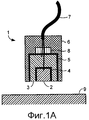
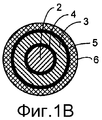
Существующие емкостные датчики обычно являются большими как по высоте, так и по площади датчика. На чертежах фиг.1A и фиг.1B показана конструкция емкостного датчика из предшествующего уровня техники. На чертеже фиг.1A датчик-зонд показан на виде в разрезе, а на чертеже фиг.1B он показан на виде с торца. Проводящий измерительный электрод 2 окружен проводящим охранным электродом 3. Изолирующий слой 4 разделяет эти два электрода, а другой изолирующий слой 5 может использоваться для отделения охранного электрода 3 от корпуса 6. Электрический кабель 7 и соединитель 8 соединяют датчик с системой обработки сигналов для получения желательного результирующего сигнала от измерительного прибора. Рабочий диапазон датчика зависит от измерительной области под измерительным электродом 2. Потенциал охранного электрода 3 установлен равным потенциалу измерительного электрода для ограничения электрического поля в пределах измерительной области для генерации относительно однородного электрического поля между измерительным электродом 2 и мишенью 9. Конструкция этого типа приводит к относительно высокому датчику, как правило, высотой около 20 мм, и к относительно большому измерительному электроду.Existing capacitive sensors are usually large in both height and sensor area. On the drawings figa and figv shows the construction of a capacitive sensor from the prior art. In the drawing of FIG. 1A, the sensor probe is shown in sectional view, and in the drawing of FIG. 1B, it is shown in end view. The conductive measuring
Относительно большая высота и ширина датчиков требуют, чтобы датчики были расположены относительно далеко от проекционного объектива, что вносит погрешности вследствие изменения относительного позиционирования датчиков и проекционного объектива вследствие производственных допусков и теплового расширения. Относительно большой размер существующих емкостных зондов также требует, чтобы отдельные датчики в конфигурациях с множеством датчиков были расположены относительно далеко друг от друга, что уменьшает пространственное разрешение измерительной системы, вследствие чего могут не обнаруживаться неровности на поверхности полупроводниковой пластины, имеющие место на небольшой площади поверхности полупроводниковой пластины. Относительно большое расстояние между ними также приводит к более медленной процедуре измерений, что уменьшает производительность литографической машины, в которой используют эти системы.The relatively large height and width of the sensors require that the sensors are located relatively far from the projection lens, which introduces errors due to changes in the relative positioning of the sensors and the projection lens due to manufacturing tolerances and thermal expansion. The relatively large size of existing capacitive probes also requires that individual sensors in configurations with many sensors are located relatively far from each other, which reduces the spatial resolution of the measuring system, as a result of which irregularities on the surface of the semiconductor wafer that occur on a small surface area of the semiconductor plates. The relatively large distance between them also leads to a slower measurement procedure, which reduces the performance of the lithographic machine in which these systems are used.
В патенте Великобритании № 2131176 описан емкостной зонд для измерения расстояния, изготовленный путем склеивания друг с другом двух термопластических полимерных пленок с покрытием из меди, нанесенным на одну сторону так, чтобы покрытая медью лицевая сторона одного листа была соединена с лицевой стороной другого листа, не имеющей покрытия. Экспонируемое покрытие из меди на одном листе разделено на первую область, которая образует измерительный электрод, и вторую область, которая, по меньшей мере, частично окружает измерительный электрод и электрически связана с покрытием из меди на другом листе, образуя охранный электрод для измерительного электрода. Эта конструкция имитирует конструкцию, показанную на чертеже фиг.1, обеспечивая наличие охранного электрода, окружающего измерительный электрод, причем оба электрода: охранный электрод, окружающий измерительный электрод, и измерительный электрод сформированы на одной и той же поверхности и на одном и том же уровне многослойного устройства. Это приводит к конструкции, которая требует наличия электрического соединения между различными проводящими слоями и соответственно требует более сложного и дорогостоящего технологического процесса изготовления.United Kingdom Patent No. 2131176 describes a capacitive distance measuring probe made by gluing together two thermoplastic polymer films coated with copper on one side so that the copper coated face of one sheet is connected to the face of another sheet that does not have coverings. The copper coating on one sheet is divided into a first region that forms the measuring electrode and a second region that at least partially surrounds the measuring electrode and is electrically connected to the copper coating on the other sheet, forming a guard electrode for the measuring electrode. This design mimics the design shown in FIG. 1, providing a security electrode surrounding the measuring electrode, both electrodes: the security electrode surrounding the measuring electrode and the measuring electrode being formed on the same surface and on the same level of the multilayer devices. This leads to a design that requires an electrical connection between the various conductive layers and accordingly requires a more complex and expensive manufacturing process.
Кроме того сложно создать проводные соединения с этими датчиками, и межсоединения вносят емкости, которые влияют на показания датчика и которые необходимо учитывать, обычно датчик калибруют совместно с проложенными межсоединениями. Необходимость калибровки существующих датчиков совместно с межсоединениями датчиков требует повторной калибровки всякий раз, когда производится замена датчика, что делает эту замену сложной, трудоемкой и дорогостоящей.In addition, it is difficult to create wired connections with these sensors, and the interconnections introduce capacities that affect the sensor readings and which must be taken into account, usually the sensor is calibrated together with the laid interconnects. The need to calibrate existing sensors in conjunction with sensor interconnects requires re-calibration whenever a sensor is replaced, which makes this replacement difficult, time consuming and expensive.
В патенте США № 4538069 описан способ калибровки емкостного датчика высоты для литографической машины с одним пучком электронов для экспонирования шаблонов. Датчик высоты сначала калибруют в калибровочном приспособлении с использованием лазерного интерферометра, и устройство затем переставляют в литографическую станцию для экспонирования шаблона, и расстояние до шаблона измеряют емкостным датчиком. Емкостные датчики сформированы на подложке, которая прикреплена к основанию корпуса системы фокусировки электронного пучка. Шаблон-мишень заземлен, емкостные датчики приводят в действие сигналами, сдвинутыми по фазе на 180°, и выходной сигнал с каждого датчика обрабатывают по отдельности для генерации четырех сигналов измерения высоты.US Pat. No. 4,538,069 describes a method for calibrating a capacitive height sensor for a lithographic machine with one electron beam for exhibiting patterns. The height sensor is first calibrated in a calibration device using a laser interferometer, and the device is then moved to a lithographic station to expose the template, and the distance to the template is measured by a capacitive sensor. Capacitive sensors are formed on a substrate that is attached to the base of the body of the electron beam focusing system. The target pattern is grounded, the capacitive sensors are driven by 180 ° phase-shifted signals, and the output signal from each sensor is processed separately to generate four height measurement signals.
СУЩНОСТЬ ИЗОБРЕТЕНИЯSUMMARY OF THE INVENTION
В настоящем изобретении предпринята попытка устранения или уменьшения вышеупомянутых недостатков для создания усовершенствованной емкостной измерительной системы, содержащей датчик, имеющий тонкопленочную структуру, причем эта тонкопленочная структура содержит датчик, имеющий первый изолирующий слой и первую проводящую пленку, которая содержит измерительный электрод, сформированный на первой поверхности первого изолирующего слоя, и вторую проводящую пленку, содержащую задний охранный электрод. Задний охранный электрод сформирован в одной плоскости и содержит периферийную часть в той же самой плоскости и расположен на второй поверхности первого изолирующего слоя и первой поверхности второго изолирующего слоя или защитного слоя. Периферийная часть заднего охранного электрода продолжается за пределы измерительного электрода, образуя боковой охранный электрод, который по существу или полностью окружает измерительный электрод.The present invention has attempted to eliminate or reduce the aforementioned disadvantages to provide an improved capacitive measuring system comprising a sensor having a thin film structure, the thin film structure comprising a sensor having a first insulating layer and a first conductive film that comprises a measuring electrode formed on a first surface of the first an insulating layer, and a second conductive film containing a rear guard electrode. The back guard electrode is formed in one plane and contains a peripheral part in the same plane and is located on the second surface of the first insulating layer and the first surface of the second insulating layer or protective layer. The peripheral part of the back guard electrode extends beyond the limits of the measuring electrode, forming a side guard electrode, which essentially or completely surrounds the measuring electrode.
В этой конструкции датчика отсутствуют отдельные боковые охранные электроды, сформированные на том же самом уровне, что и измерительный электрод, и отсутствует электрическое соединение между отдельным боковым охранным электродом и задним охранным электродом, при этом, тем не менее, достигнута конструкция высокоточного датчика. В тонкопленочном датчике малого размера, предложенном в настоящем изобретении, это электрическое соединение делает процесс изготовления более сложным и дорогостоящим, требуя таких мер как межслойный переход через изолирующий слой или дополнительные внешние проводные соединения. Изобретение подразумевает понимание того, что боковой охранный электрод может быть сформирован из периферийного участка заднего охранного электрода, поэтому боковой охранный электрод и задний охранный электрод сформированы как одна пленка в одной и той же плоскости, например, сформированы на одной и той же поверхности изолирующего слоя. В этой конструкции устранены сложности, обязательно возникающие при создании электрического соединения с отдельным боковым охранным электродом. На основании объединенных вариантов реализации, заключающихся в том, что силовые линии поля заднего охранного электрода продолжаются поперечно плоскости заднего охранного электрода и толщине изолирующего слоя между измерительным электродом, и что задний охранный электрод имеет настолько малую высоту, что охранный электрод не обязательно должен быть расположен на точно той же высоте (то есть в той же самой плоскости), что и измерительный электрод, отдельный боковой охранный электрод, окружающий измерительный электрод, расположенный в той же самой плоскости, что и измерительный электрод, может отсутствовать. Эта конструкция датчика отклоняется от предыдущих трубчатых конструкций и тонкопленочного эквивалента этой конструкции, в которых боковой охранный электрод сформирован в той же самой плоскости, что и измерительный электрод, что приводит к простому и дешевому в изготовлении, но точному датчику, который может применяться более широко и легко.In this sensor design, there are no separate side guard electrodes formed at the same level as the measuring electrode, and there is no electrical connection between the separate side guard electrode and the rear guard electrode, however, the design of a high-precision sensor is achieved. In the small-size thin-film sensor of the present invention, this electrical connection makes the manufacturing process more complex and expensive, requiring measures such as interlayer transition through the insulating layer or additional external wire connections. The invention implies the understanding that the side guard electrode can be formed from the peripheral portion of the back guard electrode, therefore, the side guard electrode and the back guard electrode are formed as one film in the same plane, for example, are formed on the same surface of the insulating layer. This design eliminates the difficulties that necessarily arise when creating an electrical connection with a separate side guard electrode. Based on the combined implementation options, namely, that the field lines of the back guard electrode extend across the plane of the back guard electrode and the thickness of the insulating layer between the measuring electrode, and that the back guard electrode is so small that the guard electrode does not have to be located on exactly the same height (i.e. in the same plane) as the measuring electrode, a separate side guard electrode surrounding the measuring electrode located in t the same plane as the measuring electrode may be absent. This sensor design deviates from previous tubular structures and the thin-film equivalent of this design, in which the side guard electrode is formed in the same plane as the measuring electrode, which leads to a simple and cheap to manufacture, but accurate sensor, which can be used more widely and easily.
Емкостная измерительная система может дополнительно содержать удлиненный соединительный элемент, содержащий гибкую мембрану, на которой напечатаны или к которой прикреплены токопроводящие дорожки, причем эти токопроводящие дорожки электрически соединены с измерительным электродом и с задним охранным электродом датчика на одном конце и с соединителем на другом конце. Изолирующий слой может содержать первую область, где сформирован измерительный электрод, и вторую удлиненную область, в которой сформированы токопроводящие дорожки.The capacitive measuring system may further comprise an elongated connecting element comprising a flexible membrane on which conductive paths are printed or attached, and these conductive paths are electrically connected to the measuring electrode and to the rear guard electrode of the sensor at one end and with a connector at the other end. The insulating layer may comprise a first region where a measuring electrode is formed and a second elongated region in which conductive paths are formed.
Тонкопленочная структура может дополнительно содержать третью проводящую пленку, содержащую экранирующий электрод, расположенный на второй поверхности второго изолирующего слоя. Эта тонкопленочная структура может дополнительно содержать удлиненный соединительный элемент, содержащий гибкую мембрану, на которой напечатаны или к которой прикреплены токопроводящие дорожки, причем эти токопроводящие дорожки электрически соединены, по меньшей мере, с измерительным электродом и с задним охранным электродом измерительного электрода, с задним охранным электродом и с экранирующим электродом (44) датчика на одном конце и с соединителем на другом конце. Датчик может быть соединен с трехжильным коаксиальным кабелем, а экранирующий электрод может быть электрически соединен с его внешней заземленной электрической жилой.The thin film structure may further comprise a third conductive film comprising a shielding electrode located on a second surface of the second insulating layer. This thin film structure may further comprise an elongated connecting element comprising a flexible membrane on which conductive paths are printed or attached, and these conductive paths are electrically connected to at least the measuring electrode and the rear guard electrode of the measuring electrode, and the rear guard electrode and with a shield electrode (44) of the sensor at one end and with a connector at the other end. The sensor can be connected to a three-wire coaxial cable, and the shield electrode can be electrically connected to its external grounded electrical core.
Емкостная измерительная система также может содержать источник питания переменного тока для подачи питания на емкостной датчик, схему обработки сигналов для обработки сигналов от датчика и трехжильный коаксиальный кабель для соединения емкостного датчика с источником питания переменного тока и схемой обработки сигналов, причем этот кабель имеет центральную жилу, внешнюю жилу и экранирующую жилу, где центральная жила предназначена для электрического соединения источника питания переменного тока с измерительным электродом датчика, внешняя жила предназначена для электрического соединения с задним охранным электродом датчика, а экранирующая жила предназначена для электрического соединения экранирующего электрода датчика с заземлением схемы обработки сигналов на удаленном от датчиков конце кабеля.The capacitive measuring system may also include an AC power source for supplying power to the capacitive sensor, a signal processing circuit for processing signals from the sensor, and a three-wire coaxial cable for connecting the capacitive sensor to an AC power source and a signal processing circuit, this cable having a central core, the outer core and the shielding core, where the central core is designed to electrically connect the AC power source to the sensor’s measuring electrode, in The external core is intended for electrical connection with the rear guard electrode of the sensor, and the screening core is intended for electrical connection of the screening electrode of the sensor with grounding of the signal processing circuit at the cable end remote from the sensors.
В другом аспекте настоящее изобретение относится к емкостной измерительной системе, содержащей датчик, имеющий тонкопленочную структуру, причем эта тонкопленочная структура содержит датчик, имеющий первый изолирующий слой, первую проводящую пленку, содержащую измерительный электрод, сформированный на первой поверхности первого изолирующего слоя, вторую проводящую пленку, содержащую задний охранный электрод, расположенный на второй поверхности первого изолирующего слоя и первой поверхности второго изолирующего слоя, и третью проводящую пленку, содержащую экранирующий электрод, расположенный на второй поверхности второго изолирующего слоя. Этот датчик прикреплен к структуре и электрически соединен с трехжильным коаксиальным кабелем, причем экранирующий электрод датчика электрически соединен с внешней жилой трехжильного коаксиального кабеля для обеспечения соединения с потенциалом земли на удаленном от датчиков конце кабеля, а экранирующий электрод датчика не имеет электрического соединения со структурой в датчике.In another aspect, the present invention relates to a capacitive measuring system comprising a sensor having a thin film structure, said thin film structure comprising a sensor having a first insulating layer, a first conductive film comprising a measuring electrode formed on a first surface of a first insulating layer, a second conductive film, comprising a rear guard electrode located on a second surface of the first insulating layer and a first surface of the second insulating layer, and a third wire yaschuyu film comprising a shield electrode disposed on the second surface of the second insulating layer. This sensor is attached to the structure and electrically connected to a three-core coaxial cable, the sensor shielding electrode being electrically connected to the external core of the three-core coaxial cable to provide ground potential at the cable end remote from the sensors, and the sensor shielding electrode is not electrically connected to the structure in the sensor .
Электроды датчика могут быть соединены с соответствующими жилами трехжильного коаксиального кабеля через тонкопленочный соединительный элемент. Электроды датчика могут быть соединены с жилами кабеля через токопроводящие дорожки на тонкопленочном соединителе, причем эти токопроводящие дорожки электрически соединены, по меньшей мере, с измерительным электродом и с задним охранным электродом датчика на одном конце, и с соединителем на другом конце. Одна или более токопроводящих дорожек, электрически соединенных с задним охранным электродом, могут быть расположены так, что лежат над токопроводящей дорожкой, соединенной с измерительным электродом, при этом токопроводящие дорожки, электрически соединенные с задним охранным электродом, являются более широкими, вследствие чего периферийная часть продолжается за пределы края токопроводящей дорожки, соединенной с измерительным электродом. Система может дополнительно содержать одну или более токопроводящих дорожек, соединенных с экранирующим электродом датчика на одном конце и электрически соединенных с внешней электрической жилой кабеля, имеющей потенциал земли, на другом конце. Одна или более токопроводящих дорожек, электрически соединенных с экранирующим электродом, могут быть расположены так, что лежат над токопроводящей дорожкой, соединенной с задним охранным электродом, и токопроводящей дорожкой, соединенной с измерительным электродом.The sensor electrodes can be connected to the corresponding cores of a three-core coaxial cable through a thin-film connecting element. The sensor electrodes can be connected to the cable conductors through conductive paths on a thin-film connector, and these conductive paths are electrically connected to at least the measuring electrode and the rear guard electrode of the sensor at one end and to the connector at the other end. One or more conductive paths electrically connected to the rear guard electrode may be positioned so as to lie above the conductive path connected to the measuring electrode, the conductive paths electrically connected to the rear guard electrode being wider, as a result of which the peripheral portion continues beyond the edge of the conductive path connected to the measuring electrode. The system may further comprise one or more conductive paths connected to a sensor shielding electrode at one end and electrically connected to an external electrical core cable having ground potential at the other end. One or more conductive paths electrically connected to the shield electrode may be positioned so as to lie above the conductive path connected to the rear guard electrode and the conductive path connected to the measurement electrode.
Изолирующие слои емкостной измерительной системы могут совместно использоваться с дополнительными емкостными датчиками, а тонкопленочная структура может быть гибкой. Изолирующие слои могут содержать листы из каптона, или подложку из пирекса, или кремниевую подложку с изоляционным покрытием.The insulating layers of a capacitive measuring system can be shared with additional capacitive sensors, and the thin-film structure can be flexible. The insulating layers may comprise kapton sheets, or a pyrex substrate, or a silicon substrate with an insulating coating.
В еще одном аспекте настоящее изобретение также относится к литографической системе для экспонирования мишени, причем эта система содержит систему проекционного объектива для фокусировки экспонирующего пучка на мишень, подвижный координатный стол для транспортировки мишени, емкостную измерительную систему (согласно любому из описанных выше вариантов) для выполнения измерений, связанных с расстоянием между системой проекционного объектива и мишенью, и блок управления для управления перемещением подвижного координатного стола для регулировки положения мишени, по меньшей мере, частично на основании сигнала из емкостной измерительной системы.In another aspect, the present invention also relates to a lithographic system for exhibiting a target, the system comprising a projection lens system for focusing the exposure beam on the target, a movable coordinate table for transporting the target, a capacitive measuring system (according to any of the above options) for performing measurements associated with the distance between the projection lens system and the target, and a control unit for controlling the movement of the moving coordinate table for p gulirovki position of the target at least partially based on the signal of a capacitive measuring system.
КРАТКОЕ ОПИСАНИЕ ЧЕРТЕЖЕЙBRIEF DESCRIPTION OF THE DRAWINGS
Ниже будет приведено объяснение различных аспектов настоящего изобретения со ссылкой на варианты его осуществления, показанные на чертежах, на которых изображено следующее:Below will be an explanation of various aspects of the present invention with reference to the options for its implementation, shown in the drawings, which depict the following:
на чертеже фиг.1A изображен емкостной датчик на виде в разрезе;on the drawing figa depicts a capacitive sensor in a sectional view;
на чертеже фиг.1B емкостной датчик из фиг.1A показан на виде с торца;1B, the capacitive sensor of FIG. 1A is an end view;
на чертеже фиг.2 изображена упрощенная схема расположения электродов в виде параллельных пластин;the drawing of figure 2 shows a simplified arrangement of electrodes in the form of parallel plates;
на чертеже фиг.3 изображена схема емкостного датчика-зонда и заземленной проводящей мишени;the drawing of figure 3 shows a diagram of a capacitive sensor probe and a grounded conductive target;
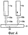
на чертеже фиг.4 изображена схема двух емкостных датчиков-зондов в компоновке для дифференциальных измерений с заземленной проводящей мишенью;the drawing of figure 4 shows a diagram of two capacitive sensors probes in the layout for differential measurements with a grounded conductive target;
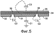
на чертеже фиг.5 на виде в разрезе изображен емкостной датчик, содержащий тонкопленочную структуру;in the drawing of FIG. 5, a sectional view shows a capacitive sensor comprising a thin film structure;
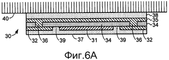
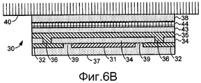
на чертежах фиг.6A, фиг.6B, фиг.6C и фиг.6D на виде в разрезе изображены различные варианты осуществления тонкопленочного датчика;in the drawings of FIG. 6A, FIG. 6B, FIG. 6C and FIG. 6D, a sectional view shows various embodiments of a thin film sensor;
на чертеже фиг.6E на виде сверху изображен датчик из фиг.6A и 6B;in the drawing of FIG. 6E, a top view shows the sensor of FIGS. 6A and 6B;
на чертеже фиг.6F на виде сверху изображен датчик из фиг.6D;on the drawing fig.6F in a top view shows the sensor of fig.6D;
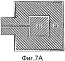
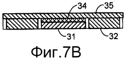
на чертеже фиг.7A на виде сверху изображен тонкопленочный датчик с квадратным измерительным электродом;on the drawing figa in a top view shows a thin-film sensor with a square measuring electrode;
на чертеже фиг.7B на виде в разрезе изображен датчик из фиг.8A;on the drawing figv in a sectional view shows the sensor of figa;
на чертеже фиг.8A на виде сверху изображен тонкопленочный датчик с круглым измерительным электродом;on the drawing figa in a top view shows a thin-film sensor with a round measuring electrode;
на чертеже фиг.8B на виде в разрезе изображен датчик из фиг.8A;on the drawing figv in a sectional view shows the sensor of figa;
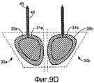
на чертежах фиг.9A, фиг.9B и фиг.9C на виде в разрезе изображены различные варианты осуществления интегрального дифференциального тонкопленочного датчика;in the drawings of FIGS. 9A, FIG. 9B and FIG. 9C, a sectional view shows various embodiments of an integrated differential thin-film sensor;
на чертеже фиг.9D на виде сверху изображен интегральный дифференциальный тонкопленочный датчик;on the drawing fig.9D in a top view shows the integral differential thin-film sensor;
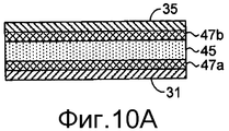
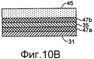
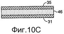
на чертежах фиг.10A-фиг.10D на виде в разрезе изображены тонкопленочные емкостные датчики;in the drawings of FIGS. 10A-10D, a sectional view shows thin-film capacitive sensors;
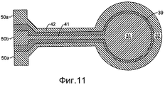
на чертеже фиг.11 на виде сверху изображен датчик с соединительными шинами и контактными площадками;in the drawing of Fig.11 in a top view shows a sensor with connecting buses and pads;
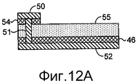
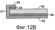
на чертежах фиг.12A и фиг.12B на виде в разрезе изображены структуры контактных площадок;on the drawings figa and figv in a view in section shows the structure of the contact pads;
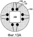
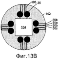
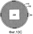
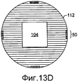
на чертежах фиг.13A-фиг.13D изображены схемы датчиков, соединительных шин и контактных площадок, сформированных на общей подложке;on the drawings figa-fig.13D shows a diagram of the sensors, connecting buses and pads formed on a common substrate;
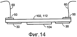
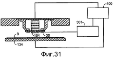
на чертеже фиг.14 на виде сбоку изображены датчики, установленные на литографической машине;in the drawing of Fig.14 in a side view shows sensors mounted on a lithographic machine;
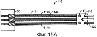
на чертежах фиг.15A и фиг.15B изображены схемы гибкого печатного соединителя;on the drawings figa and figb depicts a diagram of a flexible printed connector;
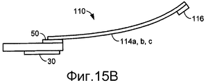
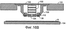
на чертежах фиг.16A и фиг.16B на виде в разрезе изображена стопа линз проекционного объектива литографической машины, в которой применяют заряженные частицы;in the drawings of Figs. 16A and 16B, a sectional view shows a stack of lenses of a projection lens of a lithographic machine in which charged particles are used;
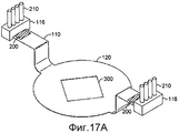
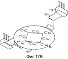
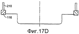
на чертежах фиг.17A-фиг.17D изображены схемы конструкции гибкой печатной платы с множеством датчиков и интегрированными гибкими печатными соединителями;on the drawings figa-fig.17D shows a design diagram of a flexible printed circuit board with many sensors and integrated flexible printed connectors;
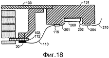
на чертеже фиг.18 изображена другая компоновка соединений датчиков на литографической машине;on the drawing of Fig. 18 shows another arrangement of sensor connections on a lithographic machine;
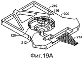
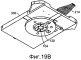
на чертежах фиг.19A и фиг.19B изображены схемы компоновок для монтажа конструкции, представляющей собой интегральную гибкую печатную плату, на литографической машине;on the drawings figa and fig.19B shows the layout diagrams for mounting the structure, which is an integrated flexible printed circuit board, on a lithographic machine;
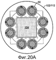
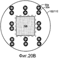
на чертежах фиг.20A и фиг.20B изображены схемы конфигураций емкостных датчиков на монтажной пластине;the drawings of FIG. 20A and FIG. 20B show configuration diagrams of capacitive sensors on a mounting plate;
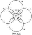
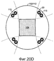
на чертежах фиг.20C и фиг.20D изображены схемы емкостных датчиков, расположенных в диагональной конфигурации;on the drawings fig.20C and fig.20D shows a diagram of capacitive sensors located in a diagonal configuration;
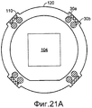
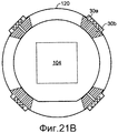
на чертежах фиг.21A и фиг.21B изображены схемы тонкопленочной структуры со сформированным на ней множеством емкостных датчиков;on the drawings figa and figv depicts a diagram of a thin-film structure formed on it with a lot of capacitive sensors;
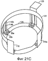
на чертеже фиг.21C изображена схема конструкции гибкой печатной платы с множеством датчиков и интегрированными гибкими печатными соединителями;21C shows a design diagram of a flexible printed circuit board with a plurality of sensors and integrated flexible printed connectors;
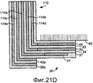
на чертеже фиг.21D на виде в разрезе изображен интегрированный гибкий печатный соединитель;21D is a cross-sectional view illustrating an integrated flexible print connector;
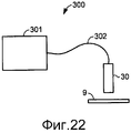
на чертеже фиг.22 изображена блок-схема системы датчиков и системы обработки сигналов;22 is a block diagram of a sensor system and a signal processing system;
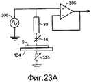
на чертеже фиг.23A изображена упрощенная принципиальная электрическая схема высокоимпедансного усилителя с источником тока;23A is a simplified circuit diagram of a high impedance amplifier with a current source;
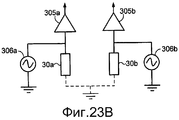
на чертеже фиг.23B изображена упрощенная принципиальная электрическая схема устройства дифференциального датчика с источником тока;23B is a simplified circuit diagram of a differential sensor device with a current source;
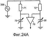
на чертеже фиг.24A изображена упрощенная принципиальная электрическая схема устройства моста Уитстона с источником напряжения;24A is a simplified circuit diagram of a Wheatstone bridge device with a voltage source;
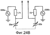
на чертеже фиг.24B изображена упрощенная принципиальная электрическая схема устройства дифференциального датчика с источником напряжения;24B is a simplified circuit diagram of a differential sensor device with a voltage source;
на чертеже фиг.25 изображена упрощенная принципиальная электрическая схема цепи дифференциального датчика;25 is a simplified circuit diagram of a differential sensor circuit;
на чертеже фиг.26 изображена упрощенная принципиальная электрическая схема синхронного детектора;the drawing of Fig.26 shows a simplified circuit diagram of a synchronous detector;
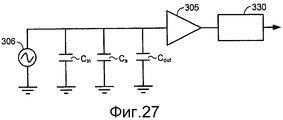
на чертеже фиг.27 изображена блок-схема, на которой показаны емкости в системе датчика;Fig. 27 is a block diagram showing capacities in a sensor system;
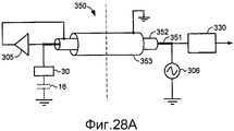
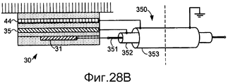
на чертежах фиг.28A и фиг.28B изображены упрощенные схемы соединения устройства с кабелем, соединяющим датчик со схемой обработки сигналов;the drawings of FIG. 28A and FIG. 28B show simplified connection diagrams of the device with a cable connecting the sensor to a signal processing circuit;
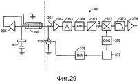
на чертеже фиг.29 изображена упрощенная принципиальная электрическая схема другого варианта осуществления синхронной схемы;29 is a simplified circuit diagram of another embodiment of a synchronous circuit;
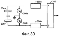
на чертеже фиг.30 изображена упрощенная принципиальная электрическая схема устройства обработки сигналов из дифференциальной пары датчиков;on the drawing of Fig.30 shows a simplified circuit diagram of a device for processing signals from a differential pair of sensors;
на чертеже фиг.31 изображена блок-схема системы управления для позиционирования полупроводниковой пластины для литографической машины; иFig. 31 is a block diagram of a control system for positioning a semiconductor wafer for a lithographic machine; and
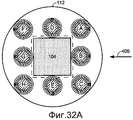
на чертежах фиг.32A и фиг.32B изображены схемы компоновки датчиков для использования с системой управления из фиг.31.in the drawings of FIG. 32A and FIG. 32B, sensor arrangement diagrams for use with the control system of FIG. 31 are shown.
ОПИСАНИЕ ВАРИАНТОВ ОСУЩЕСТВЛЕНИЯ ИЗОБРЕТЕНИЯ,DESCRIPTION OF EMBODIMENTS OF THE INVENTION
ПРИВЕДЕННЫХ В КАЧЕСТВЕ ИЛЛЮСТРАТИВНЫХ ПРИМЕРОВBASED AS ILLUSTRATIVE EXAMPLES
Ниже дано описание различных вариантов осуществления настоящего изобретения, приведенных просто в качестве примера, и со ссылкой на чертежи.The following is a description of various embodiments of the present invention, given merely as an example, and with reference to the drawings.
Теория емкостных датчиковTheory of Capacitive Sensors
В емкостном датчике используют однородное электрическое поле, созданное между двумя проводящими поверхностями. На коротких расстояниях приложенное напряжение является пропорциональным расстоянию между поверхностями. Датчики с одной пластины измеряют расстояние между одной пластиной датчика и электропроводящей поверхностью мишени.A capacitive sensor uses a uniform electric field created between two conductive surfaces. At short distances, the applied voltage is proportional to the distance between the surfaces. Sensors from one plate measure the distance between one plate of the sensor and the electrically conductive surface of the target.
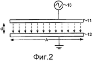
На чертеже фиг.2 показана схема расположения электродов в виде параллельных пластин. Емкость между двумя электродами 11, 12 задана зарядом, индуцированным на одном из электродов вследствие разности потенциалов между этими двумя электродами, деленным на разность потенциалов, как представлено в уравнении (1)The drawing of figure 2 shows the arrangement of the electrodes in the form of parallel plates. The capacitance between the two
![]()
![]()
![]()
![]()
Два параллельных электрода разнесены на расстояние ![]()
![]()
![]()
![]()
![]()
![]()
где ![]()
![]()
![]()
![]()
![]()
![]()
![]()
![]()
![]()
![]()
Когда для зарядки конденсатора с параллельными пластинами используют источник 13 переменного электрического тока, то между электродами создается потенциал напряжения, зависящий от импеданса электродов. Импеданс конденсатора с параллельными пластинами задается уравнением (3),When an alternating electric
![]()
![]()
![]()
![]()
где ![]()
![]()
![]()
![]()
![]()
![]()
Из уравнения (3) можно увидеть, что емкостной импеданс является обратно пропорциональным величине емкости и частоте сигнала, подаваемого на конденсатор. В случае емкостного датчика измеряют изменение электрического параметра (напряжения или тока), которое соответствует изменению импеданса датчика. Когда частота сигнала, подаваемого на датчик, сохраняется постоянной, то может быть сделано, что импеданс является обратно пропорциональным изменению емкости. Уравнение (2) показывает, что емкость является прямо пропорциональной площади зоны перекрытия электродов датчика и обратно пропорциональной изменению расстояния между электродами. Объединение уравнений (2) и (3) дает следующее уравнение:From equation (3) it can be seen that the capacitive impedance is inversely proportional to the value of the capacitance and the frequency of the signal supplied to the capacitor. In the case of a capacitive sensor, a change in the electrical parameter (voltage or current) is measured, which corresponds to a change in the sensor impedance. When the frequency of the signal supplied to the sensor is kept constant, it can be done that the impedance is inversely proportional to the change in capacitance. Equation (2) shows that the capacitance is directly proportional to the area of the overlapping zone of the sensor electrodes and inversely proportional to the change in the distance between the electrodes. Combining equations (2) and (3) gives the following equation:
![]()
![]()
![]()
![]()
где ![]()
![]()
За счет сохранения площади зоны перекрытия электродов и частоты электрического сигнала (тока), подаваемого на датчик, постоянными, изменение расстояния между электродами приводит к изменению импеданса емкостного датчика. Напряжение на датчике будет пропорциональным импедансу и пропорциональным расстоянию (![]()
![]()
Принцип измерения для емкостного датчикаMeasuring principle for capacitive sensor
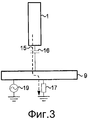
На чертеже фиг.3 показан один емкостной датчик-зонд 1, измеряющий зазор до заземленной проводящей мишени 9. Когда на него подают переменный ток, то ток течет по пути 15 от датчика до мишени через емкость 16 "датчик-мишень" и от мишени на землю через импеданс 17 "мишень-земля". Возмущения от внешних воздействий или изменений, которые влияют на измерение расстояния, представлены в схеме как напряжение 19. Точность измерения расстояния от датчика до мишени зависит от того, насколько точно датчик может измерять емкость 16 "датчик-мишень". Емкость импеданса 17 "мишень-земля" часто значительно превышает емкость 16 "датчик-мишень" и может превышать ее более чем в 100 раз, когда мишень не является хорошо заземленной. Эта высокая емкость приводит к низкому импедансу 17, поэтому ее влияние на датчик мало. Однако изменения импеданса 17 влияют на измерение расстояния, и это влияние желательно минимизировать.The drawing of figure 3 shows one
На чертеже фиг.4 показана компоновка двух емкостных датчиков-зондов 1a и 1b для дифференциального измерения зазора до мишени 9. На датчики подают переменный ток со сдвигом по фазе на 180 градусов, чтобы ток протекал по пути 18 из одного датчика до мишени через емкость 16a "датчик-мишень" и от мишени к другому датчику через другую емкость 16b "датчик-мишень". Эта компоновка для возбуждения двух датчиков сигналами, сдвинутыми по фазе, является эффективной для предотвращения протекания тока через мишень на землю и минимизирует влияние мишени на импеданс 17 заземления. Она также полезна для незаземленной мишени, поскольку обеспечивает возможность протекания тока из одного датчика в другой без необходимости наличия заземленного обратного пути. Эта компоновка с возбуждением датчиков сигналами, сдвинутыми по фазе, может использоваться в обычной системе измерений, в которой получают отдельные и независимые результаты измерения емкости (и расстояния) от каждого датчика из пары датчиков. Каждый датчик измеряет расстояние до мишени индивидуально. Возмущение 19 представлено на чертеже фиг.4 двумя напряжениями 19a и 19b возмущения, причем каждая половина величины напряжения 19 относится к синфазному возмущению, которое оказывает одинаковое влияние на каждый датчик.The drawing of figure 4 shows the layout of two capacitive sensors probes 1a and 1b for differential measurement of the gap to the
Компоновка для дифференциальных измерений также может использоваться совместно с сигналами, сдвинутыми по фазе, которые подают на датчики. В этой компоновке выходные сигналы с двух датчиков объединяют в пару таким образом, что емкость 16a "датчик-мишень" датчика 1a заряжается напряжением возбуждения датчика 1a в течение его положительного полупериода, а также напряжением возбуждения датчика 1b в течение его положительного полупериода, тогда как емкость 16b "датчик-мишень" датчика 1b заряжается напряжением возбуждения датчика 1b в течение его отрицательного полупериода, а также напряжением возбуждения датчика 1a в течение его отрицательного полупериода. Таким образом выходной сигнал с каждого датчика соответствует среднему расстоянию между этими двумя датчиками и мишенью.The arrangement for differential measurements can also be used in conjunction with phase-shifted signals that are applied to the sensors. In this arrangement, the output signals from the two sensors are paired so that the sensor-
Питание датчиков осуществляют сигналом напряжения треугольной формы с постоянным наклоном и амплитудой, что приводит к приблизительно прямоугольной форме сигнала электрического тока, подаваемого на емкость датчика, то есть к приблизительно постоянному положительному электрическому току в одном полупериоде и к приблизительно постоянному отрицательному электрическому току в другом полупериоде. Практически ток увеличивается до, по существу, стационарного состояния в течение каждого полупериода, вследствие чего измерения предпочтительно производят в течение последней части каждого полупериода, когда достигнут стационарный электрический ток.The sensors are supplied with a voltage signal of a triangular shape with a constant slope and amplitude, which leads to an approximately rectangular waveform of the electric current supplied to the sensor capacitance, i.e., to approximately constant positive electric current in one half-cycle and to approximately constant negative electric current in another half-period. In practice, the current rises to a substantially stationary state during each half-cycle, whereby measurements are preferably taken during the last part of each half-cycle when a stationary electric current is reached.
Ток, протекающий через датчик, и соответствующая емкость датчика могут быть измерены и преобразованы в напряжение для дальнейшей обработки. Результирующие значения для каждого датчика из дифференциальной пары могут быть объединены для уменьшения или устранения синфазных возмущений. Например, стационарный ток, протекающий через датчик 1a в течение положительного периода электрического тока, может быть просуммирован со стационарным током, протекающим через датчик 1b в течение положительного периода электрического тока, и аналогичным образом стационарный ток, протекающий через датчик 1a в течение отрицательного периода электрического тока, может быть просуммирован со стационарным током, протекающим через датчик 1b в течение отрицательного периода электрического тока. Вычитание просуммированного значения в положительном периоде из просуммированного значения в отрицательном периоде дает сигнал дифференциального датчика, то есть Vdiff=(V1pos+V2pos)-(V1neg+V2neg).The current flowing through the sensor and the corresponding sensor capacitance can be measured and converted to voltage for further processing. The resulting values for each sensor from the differential pair can be combined to reduce or eliminate common mode disturbances. For example, the stationary current flowing through the
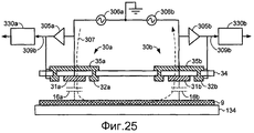
Вследствие того, что датчики расположены в непосредственной близости, и того, что возбуждение пары датчиков осуществляют со сдвигом по фазе, ток датчика заряжает и разряжает обе емкости 16a и 16b "датчик-мишень" пары датчиков так, что каждое измеренное значение равно среднему значению расстояния от каждого датчика до мишени. Оно может рассматриваться как расстояние между парой датчиков и точкой на мишени посередине между этими двумя датчиками. На каждое измеренное значение оказывают влияние любые возмущения, например, возмущения 19a и 19b, которые показаны на чертеже фиг.4. Эти возмущения присутствуют как в значениях в положительных периодах, так и в значениях в отрицательных периодах, но, по существу, удалены из результатов измерений путем вычитания положительных и отрицательных величин при получении сигнала дифференциального датчика. Преимущество этой компоновки состоит в том, что синфазные возмущения в отдельных датчиках взаимно компенсируются при измерениях. Любые различия в двух датчиках, которые остаются постоянными во время измерений, будут взаимно скомпенсированными, что приводит к точному результату измерения. Компоновка для дифференциальных измерений сильно ослабляет влияние емкости мишени относительно земли и увеличивает чувствительность системы датчиков.Due to the fact that the sensors are located in close proximity, and that the pair of sensors is phase-shifted, the sensor current charges and discharges both sensor-
Конструкция датчиковSensor Design
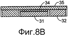
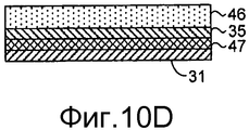
На чертеже фиг.5 на виде в разрезе показан емкостной датчик, содержащий тонкопленочную структуру. Проводящий измерительный электрод 31 и проводящий боковой охранный электрод 32 сформированы на изолирующей пленке 34 или прикреплены к ней. Проводящий задний охранный электрод 35 расположен на задней стороне изолирующей пленки 34. Зазор 39 между измерительным электродом и охранным электродом является узким, обычно равным нескольким десятым долям микрометра, и может представлять собой воздушный зазор или зазор, заполненный изоляционным материалом.In the drawing of FIG. 5, a sectional view shows a capacitive sensor comprising a thin film structure. A
Электрическое поле, сгенерированное между измерительным электродом и мишенью, искривляется вблизи краев измерительного электрода. Наличие проводника вблизи края измерительного электрода может оказывать большое и непредсказуемое влияние на электрическое поле и, следовательно, на результаты измерений посредством датчика. Чтобы избежать этой ситуации (и сделать результаты измерений посредством датчика более прогнозируемыми и более простыми для моделирования, чтобы электрическое поле можно было вычислить аналитически), измерительный электрод окружен охранным электродом, на который подают тот же самый потенциал, что и на измерительный электрод. Охранный электрод функционирует в качестве экрана против внешних помех и также выводит эффекты искривления электрического поля из измерительной области под измерительным электродом, уменьшая паразитную емкость. Электрическое поле генерируют между охранным электродом и мишенью на каждой стороне электрического поля между измерительным электродом и мишенью. Между измерительным электродом и охранным электродом сгенерированное электрическое поле отсутствует, поскольку они имеют одинаковый потенциал. Это приводит, по существу, к однородному электрическому полю в области под измерительным электродом, тогда как на внешних краях охранных электродов происходит искривление поля.The electric field generated between the measuring electrode and the target is bent near the edges of the measuring electrode. The presence of a conductor near the edge of the measuring electrode can have a large and unpredictable effect on the electric field and, therefore, on the results of measurements by means of a sensor. In order to avoid this situation (and to make the results of measurements by means of a sensor more predictable and simpler for modeling, so that the electric field can be calculated analytically), the measuring electrode is surrounded by a guard electrode, to which the same potential is applied as to the measuring electrode. The guard electrode functions as a screen against external interference and also removes the effects of the curvature of the electric field from the measuring region under the measuring electrode, reducing the stray capacitance. An electric field is generated between the guard electrode and the target on each side of the electric field between the measuring electrode and the target. There is no generated electric field between the measuring electrode and the guard electrode, since they have the same potential. This leads, in essence, to a uniform electric field in the area under the measuring electrode, while at the outer edges of the guard electrodes, the field is curved.
Площадь измерительного электрода 31 должна быть большой по сравнению с расстоянием, отделяющим измерительный электрод от мишени. К тому же, зазор 39 между измерительным электродом 31 и боковым охранным электродом 32 должен быть малым по сравнению с расстоянием между измерительным электродом и мишенью, а ширина бокового охранного электрода 32 должна быть большой по сравнению с расстоянием между измерительным электродом и мишенью. В одном из вариантов осуществления изобретения ширина измерительного электрода является, по меньшей мере, в пять раз большей, чем расстояние между электродом датчика и мишенью, зазор между измерительным электродом и охранным электродом является меньшим или равным одной пятой расстояния между электродом датчика и мишенью, а ширина охранного электрода является, по меньшей мере, в пять раз большей, чем расстояние между измерительным электродом и мишенью. Соблюдение эти сравнительных конструктивных правил обеспечивает вариант осуществления конструктивных правил для емкостного датчика с очень предсказуемой емкостью, например, предсказуемость емкости равна одной миллионной. Предсказуемость здесь определяется как относительная погрешность при использовании формулы идеальной емкости пластины в зависимости от расстояния согласно приведенному уравнению (2) для вычисления емкости для электрода конечного размера вместо электрода бесконечного размера.The area of the measuring
Помимо измеряемой емкости C1 датчика между измерительным электродом и мишенью датчик имеет собственные паразитные емкости C2 и C3 между каждым из отдельных элементов конструкции. Паразитные емкости C2 и C3 являются малыми по сравнению с измеряемой емкостью C1. В варианте осуществления изобретения, показанном на чертеже фиг.5, паразитные емкости включают в себя емкость C2 между измерительным электродом и боковыми охранными электродами и емкость C3 между измерительным электродом и задним охранным электродом.In addition to the measured capacitance C 1 of the sensor between the measuring electrode and the target, the sensor has its own parasitic capacitances C 2 and C 3 between each of the individual structural elements. Spurious capacitances C 2 and C 3 are small compared to the measured capacitance C 1 . In the embodiment of the invention shown in FIG. 5, parasitic capacitances include a capacitance C 2 between the measuring electrode and the side guard electrodes and a capacitance C 3 between the measuring electrode and the rear guard electrode.
В одном из вариантов осуществления датчика емкость C1 между измерительным электродом и мишенью составляет от 0,1 пФ до 1 пФ, тогда как паразитная емкость C2 между измерительным электродом и боковыми охранными электродами является в 100-1000 раз меньшей, обычно порядка 0,001 пФ (то есть 10-15 Ф). Паразитная емкость C3 между измерительным электродом и задним электродом обычно является большей и преобладающей, обычно она равна приблизительно от 1 пФ до 1000 пФ (то есть от 10-12 Ф до 10-9 Ф). Влияние этих паразитных емкостей уменьшено за счет подачи на охранный электрод того же самого потенциала, что и на измерительный электрод. Это может быть достигнуто путем электрического соединения бокового охранного электрода и измерительного электрода или за счет использования помощи активной защиты, которая более подробно описана ниже. Активная защита также может использоваться для заднего охранного электрода.In one embodiment of the sensor, the capacitance C 1 between the measuring electrode and the target is from 0.1 pF to 1 pF, while the stray capacitance C 2 between the measuring electrode and the side guard electrodes is 100-1000 times smaller, usually of the order of 0.001 pF ( i.e. 10-15 F). The stray capacitance C 3 between the measuring electrode and the back electrode is usually larger and predominant, usually it is from about 1 pF to 1000 pF (i.e., from 10 −12 F to 10 −9 F). The influence of these parasitic capacitors is reduced due to the supply of the same potential to the guard electrode as to the measuring electrode. This can be achieved by electrically connecting the side guard electrode and the measuring electrode or by using active protection assistance, which is described in more detail below. Active protection can also be used for the rear guard electrode.
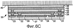
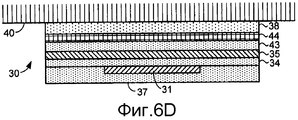
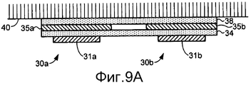
Для применения в литографических машинах, работающих в чистой производственной среде в вакуумной камере, датчики предпочтительно сконструированы так, что выделяют очень низкие уровни загрязняющих веществ, когда находятся в вакууме. Для датчиков, используемых в области применения этого типа, поверх проводников может быть сформирован защитный слой, например, из полиимидной пленки из каптона или из аналогичной защитной пленки, в особенности при использовании материалов, которые могут загрязнять вакуум. На чертежах фиг.6A-фиг.6D на виде в разрезе показаны различные варианты осуществления тонкопленочного датчика, включающего в себя защитные слои 37 и 38, на чертеже фиг.6E на виде сверху показан датчик из фиг.6A и фиг.6B, а на чертеже фиг.6F на виде сверху показан датчик из фиг.6D.For use in lithographic machines operating in a clean production environment in a vacuum chamber, the sensors are preferably designed to emit very low levels of contaminants when in vacuum. For sensors used in this type of application, a protective layer can be formed over the conductors, for example, from a polyimide film from kapton or from a similar protective film, especially when using materials that can contaminate the vacuum. In the drawings of FIG. 6A-FIG. 6D, a sectional view shows various embodiments of a thin-film sensor including
На чертеже фиг.6A на виде в разрезе показан вариант осуществления изобретения с измерительным электродом 31 и боковым охранным электродом 32, которые сформированы на одной поверхности изолирующей пленки 34 или прикреплены к ней, и с задним охранным электродом 35 на другой поверхности пленки 34. Датчик прикреплен к пластине 40, которая обычно является частью конструкции оборудования, в котором необходимо измерять расстояние, или может быть прикреплен к детали конструкции, например, к монтажной пластине или к прокладке вокруг проекционного объектива литографической машины, где датчик измеряет расстояние между проекционным объективом и полупроводниковой пластиной под объективом. Пластина 40 может быть проводящей и, следовательно, также может служить в качестве экранирующего электрода для датчика.6A is a cross-sectional view illustrating an embodiment of the invention with a measuring
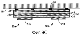
На чертеже фиг.6B показан альтернативный вариант осуществления изобретения, содержащий проводящий экранирующий электрод 44, сформированный на второй изолирующей пленке 43, служащей в качестве части конструкции датчика, или прикрепленный к ней. Эта конструкция обеспечивает возможность установки датчика на непроводящей поверхности. Даже в том случае, если он установлен на проводящей поверхности, это обеспечивает совместимость по протяженности и функционированию экранирующего электрода. Включение экранирующего электрода 44 в качестве детали конструкции датчика также обеспечивает независимый потенциал земли, который в противном случае мог быть получен с опорной поверхности. Например, когда датчик используют в литографической системе с использованием пучка электронов, на потенциал земли из машины могут оказывать влияние электрические помехи от проекционных объективов. Это также обеспечивает возможность наличия того же самого заземления экранирующего электрода датчика, что и заземление измерительных электрических цепей и кабелей, соединяющих датчик с этими электрическими цепями.FIG. 6B shows an alternative embodiment of the invention comprising a
Это может быть достигнуто путем соединения экранирующего электрода датчика с экранирующей жилой в соединительном кабеле, которая затем соединена с точкой заземления, используемой в электрических схемах измерений. Это предотвращает необходимость наличия отдельных заземлений для датчика и для измерительной электроники. Когда эта конструкция соединена трехжильным кабелем, например, трехжильным коаксиальным кабелем, она также обеспечивает возможность наличия точек соединения, приспособленных для соединения, между каждым из трех проводящих слоев датчика и соответствующей жилой трехжильного коаксиального кабеля, включая экранирующий электрод, в том числе для соединения экранирующего электрода с экранирующей жилой трехжильного коаксиального кабеля для подачи независимого потенциала земли из электрической схемы на датчик.This can be achieved by connecting the shielding electrode of the sensor to the shielding core in the connecting cable, which is then connected to the ground point used in the electrical measurement circuits. This eliminates the need for separate earths for the sensor and for the measurement electronics. When this design is connected by a three-wire cable, for example, a three-wire coaxial cable, it also provides the possibility of connecting points adapted for connection between each of the three conductive layers of the sensor and the corresponding three-wire coaxial cable, including a shield electrode, including for connecting a shield electrode with a shielded residential three-wire coaxial cable for supplying an independent ground potential from the circuitry to the sensor.
На чертеже фиг.6C проиллюстрирован другой вариант осуществления изобретения, включающий в себя внешний боковой охранный электрод 33, электрически соединенный с экранирующим электродом 44. Это соединение может быть реализовано путем формирования отверстий или межслойных переходных отверстий в изолирующих слоях 34 и 43, например, лазером, для обеспечения возможности электрического соединения между участками проводящих слоев на каждом уровне.FIG. 6C illustrates another embodiment of the invention including an external
На чертеже фиг.6D изображен еще один вариант осуществления изобретения без боковых охранных электродов на том же самом уровне или на той же самой поверхности, что и измерительный электрод. В предшествующих конструкциях, рассмотренных выше, боковые охранные электроды всегда считали необходимыми для ограничения электрического поля, сгенерированного измерительным электродом в пределах измерительной области для генерации относительно однородного электрического поля между измерительным электродом и мишенью и для уменьшения влияния проводников, расположенных близко к датчику, на датчик. В предшествующих конструкциях, которые были относительно высокими и большими, например, как показано на чертеже фиг.1A, требовался охранный электрод, который продолжался вниз до той же самой плоскости, в которой расположен электрод датчика, окружая электрод датчика. Аналогичным образом в тонкопленочных конструкциях боковые охранные электроды считали важными для размещения охранного электрода на том же самом уровне, что и электрод датчика. Боковые охранные электроды предпочтительно являются электрически соединенными с задним охранным электродом, но эта компоновка требует создания электрического соединения между этими двумя электродами, что является затруднительным. В конструкциях, показанных на чертежах фиг.6A-6C, это соединение сделано сквозь изолирующий слой 34. Вследствие небольшого размера датчика и тонкости изолирующего слоя 34 точное проделывание отверстий надлежащего размера и в надлежащем месте в изолирующем слое является затруднительным. Для этого может быть использован лазер, но технологический процесс становится более сложным и дорогостоящим.FIG. 6D shows yet another embodiment of the invention without side guard electrodes at the same level or on the same surface as the measuring electrode. In the previous designs discussed above, side guard electrodes have always been considered necessary to limit the electric field generated by the measuring electrode within the measuring region to generate a relatively uniform electric field between the measuring electrode and the target and to reduce the influence of conductors located close to the sensor on the sensor. In previous designs, which were relatively high and large, for example, as shown in FIG. 1A, a guard electrode was required that extended down to the same plane in which the sensor electrode is located, surrounding the sensor electrode. Similarly, in thin-film structures, side guard electrodes were considered important for placing the guard electrode at the same level as the sensor electrode. The side guard electrodes are preferably electrically connected to the rear guard electrode, but this arrangement requires an electrical connection between the two electrodes, which is difficult. 6A-6C, this connection is made through the insulating
Однако было установлено, что в том случае, если пленки тонкопленочного датчика являются достаточно тонкими, то боковые охранные электроды на том же самом уровне, что и измерительный электрод, не нужны. Тот же самый эффект может быть достигнут путем проектирования датчика с измерительным электродом 31 меньшего размера, чем задний охранный электрод 35, чтобы периферийная часть заднего охранного электрода выступала сбоку за его пределы и окружала измерительный электрод. В этом случае периферийная часть заднего охранного электрода действует в качестве бокового охранного электрода. Электрическое поле, исходящее из периферийной части заднего охранного электрода 35, продолжается через изолирующий слой 34, действуя так, что ограничивает электрическое поле, сгенерированное измерительным электродом, измерительной областью, вследствие чего между измерительным электродом и мишенью генерируется относительно однородное электрическое поле. Искривление электрического поля, вызванное проводником, расположенным вблизи датчика, происходит на внешних краях периферийной части заднего охранного электрода, а не в измерительном электроде. Результатом этого является более простая конструкция, которая является менее сложной в изготовлении и настолько же более дешевой в производстве, но которая может обеспечивать генерацию, по существу, однородного электрического поля в области под измерительным электродом с меньшей чувствительностью к возмущениям, вызванным проводником, расположенным близко к датчику.However, it was found that if the films of the thin-film sensor are sufficiently thin, then the side guard electrodes at the same level as the measuring electrode are not needed. The same effect can be achieved by designing a sensor with a measuring
Варианты осуществления изобретения, изображенные на чертежах фиг.6A и фиг.6B, показаны на виде сверху на чертеже фиг.6E, где измерительный электрод 31 сформирован имеющим круглую форму с C-образным боковым охранным электродом 32, почти полностью окружающим измерительный электрод, причем между этими двумя электродами остается узкий зазор вокруг периферийного края измерительного электрода 31. В этом варианте осуществления изобретения боковой охранный электрод 32 и задний электрод 35 возможно, но не обязательно, являются электрически соединенными посредством отверстия 37 в изолирующей пленке 34, обеспечивающего возможность электрического контакта между охранным и задним электродами. В этом варианте осуществления изобретения используют одно C-образное отверстие, хотя могут использоваться иные формы и/или может использоваться множество отверстий. Соединение охранного и заднего электродов приводит оба электрода к одинаковому потенциалу для устранения влияния любой емкости между ними, и влияние любой емкости между охранным и задним электродами и измерительным электродом также может быть устранено с использованием активной защиты.The embodiments of the invention depicted in the drawings of FIG. 6A and FIG. 6B are shown in a plan view of FIG. 6E, where the measuring
В варианте осуществления изобретения, показанном на чертеже фиг.6E, внутренний измерительный электрод 31 имеет одно или более продолжений, образующих соединительные шины 41 для обеспечения электрического соединения измерительного электрода с внешними схемами обработки сигналов, и аналогичным образом боковой охранный электрод 32 имеет одно или более продолжений, образующих соединительные шины 42 для обеспечения электрических соединений. Измерительный электрод 31, боковой охранный электрод 32 и соединительные шины 41 и 42 сформированы из тонких пленок. В варианте осуществления изобретения, показанном на чертеже, все электроды 31 и 32 и все соединительные шины 41 и 42 расположены в одной и той же плоскости и могут быть сформированы из одной и той же тонкой пленки путем осаждения или путем формирования частей пленки, удаляемых с использованием лазера, способом травления или иными подходящими способами удаления. Боковой охранный электрод 32, по существу, окружает измерительный электрод 31, оставляя небольшой зазор для соединительных шин 41, продолжающихся за пределами измерительного электрода, для обеспечения электрического соединения между измерительным электродом и схемами обработки сигналов. Соединительные шины также добавляют паразитные емкости, которые следует учитывать при проектировании датчика.In the embodiment of the invention shown in FIG. 6E, the
Вариант осуществления изобретения, изображенный на чертеже фиг.6D, показан на виде сверху на чертеже фиг.6F (изолирующий слой 34 не показан, поэтому виден задний охранный электрод 35). Этот вариант аналогичен варианту осуществления изобретения, показанному на чертеже фиг.6E, за исключением отсутствия боковых охранных электродов на том же самом уровне, что и измерительный электрод. На этом изображении в качестве бокового охранного электрода функционирует периферийная область 35a заднего охранного электрода 35. Датчик может быть сконструирован таким же самым образом, что и датчик из описанного выше варианта осуществления изобретения, показанного на чертеже фиг.6E, и, как описано выше, соединительные шины 41 и 42 продолжаются за пределы измерительного электрода и заднего охранного электрода для обеспечения электрических соединений.The embodiment of FIG. 6D is shown in a plan view of FIG. 6F (the insulating
В этих вариантах осуществления изобретения электроды 31 и 35 и электроды 32 и 44, когда они включены в состав конструкции, могут быть сформированы из проводящих слоев толщиной приблизительно 18 микрон, изолирующие пленки 34 и 43 могут иметь толщину приблизительно 25 микрон, а защитные слои 37, 38 могут иметь толщину приблизительно 50 микрон. Тонкопленочный датчик может быть сконструирован имеющим общую толщину приблизительно 100-200 микрон и толщину между задней поверхностью конструкции датчика и передней поверхностью измерительного электрода (то есть поверхностью, обращенной в направлении, в котором производят измерение расстояния), равную 50-150 микронам, предпочтительно около 100 микрон. Тонкопленочная структура, небольшая площадь и очень малая высота (толщина) датчика позволяют применять эти датчики в тех областях применения, где имеется лишь очень небольшое пространство (в частности, где имеющаяся высота ограничена) и где необходимо близкое расстояние между датчиками или между датчиками и другим оборудованием.In these embodiments, the
Небольшой размер тонкопленочного датчика, показанного на чертежах фиг.6A-6F (и также показанного в других вариантах осуществления изобретения, которые описаны ниже), обеспечивает много преимуществ. Тонкопленочная структура приводит к минимальной высоте, и ширина или площадь датчика также могут быть очень малыми. Это обеспечивает возможность установки датчика в непосредственной близости к той точке, в которой желательно производить измерение расстояния. При использовании датчиков в литографической машине для измерения расстояния между проекционным объективом и экспонируемой мишенью они могут быть установлены рядом с проекционным объективом и на той же самой монтажной конструкции так, чтобы как датчики, так и проекционный объектив были зафиксированы в одной и той же опорной точке. Это сильно уменьшает погрешности из-за относительного перемещения между датчиками и проекционным объективом, устраняет необходимость внесения поправок на отклонение места установки датчика от номинального и снижает требования для калибровки. Небольшой размер датчика также снижает требования к плоскостности для самого датчика.The small size of the thin-film sensor shown in FIGS. 6A-6F (and also shown in other embodiments of the invention described below) provides many advantages. The thin film structure results in a minimum height, and the width or area of the sensor can also be very small. This makes it possible to install the sensor in close proximity to the point at which it is desirable to measure the distance. When using sensors in a lithographic machine to measure the distance between the projection lens and the target being exposed, they can be mounted next to the projection lens and on the same mounting structure so that both the sensors and the projection lens are fixed at the same reference point. This greatly reduces errors due to relative movement between the sensors and the projection lens, eliminates the need for corrections for the deviation of the sensor installation location from the nominal, and reduces the requirements for calibration. The small size of the sensor also reduces flatness requirements for the sensor itself.
На чертежах фиг.7 и фиг.8 показаны дополнительные варианты осуществления тонкопленочного датчика с изолирующим слоем 34, сформированным только лишь между измерительным электродом 31 и задним электродом 35, чтобы боковой охранный электрод 32 и задний электрод 35 могли быть непосредственно соединены друг с другом.The drawings of FIG. 7 and FIG. 8 show further embodiments of a thin-film sensor with an insulating
На чертеже фиг.7A показан датчик с квадратным измерительным электродом на виде сверху, а на чертеже фиг.7B этот датчик показан на виде в разрезе. В одном из вариантов осуществления изобретения квадратный датчик спроектирован с номинальной емкостью датчика (емкостью C1 между измерительным электродом и мишенью), равной 1 пФ, при номинальном расстоянии между датчиком и мишенью, равном 100 микрон, измерительный электрод имеет ширину 3,5 мм (+/-0,01 мм) и площадь 12,25 мм2. Охранный электрод имеет ширину 1,5 мм (+/-0,01 мм), и зазор между измерительным и охранным электродами составляет 0,015 мм (+/-0,001 мм). В другом варианте осуществления изобретения датчик спроектирован с номинальной емкостью датчика, равной 10 пФ, при номинальном расстоянии между датчиком и мишенью, равном 100 микрон. Измерительный электрод имеет ширину 11 мм (+/-0,01 мм) и площадь 121 мм2. Ширина охранного электрода и зазор не изменены и равны соответственно 1,5 мм (+/-0,01 мм) и 0,015 мм (+/-0,001 мм).Fig. 7A shows a sensor with a square measuring electrode in a plan view, and in Fig. 7B, this sensor is shown in sectional view. In one embodiment of the invention, the square sensor is designed with a nominal sensor capacitance (capacitance C 1 between the measuring electrode and the target) equal to 1 pF, with a nominal distance between the sensor and the target equal to 100 microns, the measuring electrode has a width of 3.5 mm (+ / -0.01 mm) and an area of 12.25 mm 2 . The guard electrode has a width of 1.5 mm (+/- 0.01 mm), and the gap between the measuring and guard electrodes is 0.015 mm (+/- 0.001 mm). In another embodiment, the sensor is designed with a nominal sensor capacitance of 10 pF, with a nominal distance between the sensor and target of 100 microns. The measuring electrode has a width of 11 mm (+/- 0.01 mm) and an area of 121 mm 2 . The width of the guard electrode and the gap are not changed and are equal to 1.5 mm (+/- 0.01 mm) and 0.015 mm (+/- 0.001 mm, respectively).
На чертеже фиг.8A показан датчик с круглым измерительным электродом на виде сверху, а на чертеже фиг.8B этот датчик показан на виде в разрезе. В одном из вариантов осуществления изобретения круглый датчик спроектирован с номинальной емкостью датчика, равной 1 пФ, при номинальном расстоянии между датчиком и мишенью, равном 100 микрон. Измерительный электрод имеет диаметр 4 мм (+/-0,001 мм) и площадь 12,25 мм2. Охранный электрод имеет внутренний диаметр 4,015 мм (+/-0,001 мм) и внешний диаметр 8 мм (+/-0,001 мм). В другом варианте осуществления изобретения датчик спроектирован с номинальной емкостью датчика, равной 10 пФ, при номинальном расстоянии между датчиком и мишенью, равном 100 микрон. Измерительный электрод имеет диаметр 6,2 мм (+/-0,001 мм) и площадь 121 мм2. Охранный электрод имеет внутренний диаметр 6,215 мм (+/-0,001 мм) и внешний диаметр 12,4 мм (+/-0,001 мм).FIG. 8A shows a sensor with a round measuring electrode in a plan view, and FIG. 8B shows this sensor in a sectional view. In one embodiment of the invention, the circular sensor is designed with a nominal capacitance of the sensor equal to 1 pF, with a nominal distance between the sensor and the target equal to 100 microns. The measuring electrode has a diameter of 4 mm (+/- 0.001 mm) and an area of 12.25 mm 2 . The guard electrode has an inner diameter of 4.015 mm (+/- 0.001 mm) and an outer diameter of 8 mm (+/- 0.001 mm). In another embodiment, the sensor is designed with a nominal sensor capacitance of 10 pF, with a nominal distance between the sensor and target of 100 microns. The measuring electrode has a diameter of 6.2 mm (+/- 0.001 mm) and an area of 121 mm 2 . The guard electrode has an inner diameter of 6.215 mm (+/- 0.001 mm) and an outer diameter of 12.4 mm (+/- 0.001 mm).
Варианты осуществления изобретения, показанные на чертежах фиг.5-8, могут быть сконструированы так, чтобы они имели диапазон измерений (по оси z, перпендикулярной к поверхности измерительного электрода) 80-180 микрон между датчиком и мишенью. Для специалиста в данной области техники понятно, что размеры датчиков могут быть изменены для обеспечения иного диапазона измерений.The embodiments of the invention shown in the drawings of FIGS. 5-8 can be designed so that they have a measurement range (along the z axis perpendicular to the surface of the measuring electrode) of 80-180 microns between the sensor and the target. For a person skilled in the art it is clear that the size of the sensors can be changed to provide a different measurement range.
Варианты осуществления изобретения, показанные на чертежах фиг.5-8, также могут быть реализованы с использованием способов литографии для создания еще более тонких слоев материала, например, измерительного электрода 31 толщиной 100 нм (+/-10 нм), бокового охранного электрода 32 (если он содержится) и заднего электрода 35 толщиной 150 нм (+/-10 нм) и изолирующего слоя 34 толщиной 50 нм (+/-10 нм). В этих вариантах осуществления изобретения измерительный электрод является квадратным или круглым, обеспечивая большую измерительную область для максимального увеличения чувствительности датчика, одновременно обеспечивая минимизацию габаритных размеров датчика. Однако датчик может быть выполнен имеющим иную форму с измерительным электродом (и аналогичным образом с охранными электродами), выполненным в форме прямоугольника, овала или имеющим иную форму для максимального увеличения измерительной области.The embodiments of the invention shown in the drawings of figures 5-8 can also be implemented using lithography methods to create even thinner layers of material, for example, a measuring
Варианты осуществления изобретения, показанные на чертежах фиг.5-8, могут быть сконструированы с проводящим слоем для электродов 31, 32, осажденным на изолирующий слой 35 или прикрепленным к изолирующему слою клеевым или связывающим слоем. Зазор 39 между измерительным и охранным электродами может быть сформирован путем формирования единого проводящего слоя для обоих электродов: для измерительного электрода и для охранного электрода, и путем удаления материала с использованием лазера или способом травления для создания зазора. Лазер является предпочтительным для создания зазора с очень малыми значениями ширины и может быть использован для создания зазора шириной 25 микрон с малым отклонением, тогда как травление обычно обеспечивает меньшую точность.The embodiments of the invention shown in the drawings of FIGS. 5-8 can be constructed with a conductive layer for
Датчики могут быть изготовлены с использованием различных способов, например, с использованием литографических способов, технологии MEMS (микроэлектромеханических систем) или технологии гибких печатных плат. При использовании технологии гибких печатных плат изолирующий слой 34 может быть создан в виде гибкого листа или ленты из подходящего материала, например, из полиимидной пленки из каптона или из аналогичной гибкой изолирующей пленки. Проводящие электроды 31, 32 и 35 могут быть сформированы из тонкого слоя меди или иного подходящего проводящего материала, прикрепленного к изолирующему слою 34 с использованием клея, сформированы в виде слоистого материала без приклеивания, например, с использованием способа прямой металлизации, или напечатаны на изолирующем слое с использованием проводящих чернил или иными подходящими способами печати. Охранные изолирующие пленки 37 и 38 могут быть сформированы из материалов тех же самых типов, что и слой 34.The sensors can be manufactured using various methods, for example, using lithographic methods, MEMS technology (microelectromechanical systems), or flexible printed circuit technology. Using the technology of flexible printed circuit boards, the insulating
Гибкий печатный тонкопленочный датчик легко изготовить, и он может быть сделан быстро, что приводит к короткому общему времени производственного цикла. Датчик может быть сделан с надежными соединениями датчика со схемой обработки сигналов. Небольшой размер обеспечивает более высокую гибкость для его размещения в той точке, где необходимо измерять расстояние, или очень близко к ней. Датчики могут быть приклеены на месте как отдельные датчики-элементы для быстрой и простой сборки системы датчиков. Плоскостность и наклон отдельных датчиков могут быть проверены после того, как они были приклеены на месте и откалиброваны в процедуре измерения. Когда для слоев изоляции используют гибкий лист материала, то весь датчик может быть сконструирован гибким.The flexible printed thin-film sensor is easy to manufacture and can be made quickly, resulting in a short overall production cycle time. The sensor can be made with reliable sensor connections to the signal processing circuit. The small size provides greater flexibility for placing it at the point where it is necessary to measure the distance, or very close to it. The sensors can be glued in place as separate element sensors for quick and easy assembly of the sensor system. The flatness and inclination of individual sensors can be checked after they have been glued in place and calibrated in the measurement procedure. When a flexible sheet of material is used for the insulation layers, the entire sensor can be designed flexible.
Ширина зазора между измерительным и боковым охранным электродами в некоторых из вышеописанных вариантов осуществления изобретения не удовлетворяет описанным выше сравнительным конструктивным правилам, например, зазор между измерительным и охранным электродами превышает одну пятую расстояния между измерительным электродом и мишенью. Однако для многих областей применения датчиков преимущества тонкопленочной структуры перевешивают это.The width of the gap between the measuring and side guard electrodes in some of the above-described embodiments of the invention does not satisfy the comparative design rules described above, for example, the gap between the measuring and security electrodes exceeds one fifth of the distance between the measuring electrode and the target. However, for many sensor applications, the benefits of a thin film structure outweigh this.
На чертежах фиг.9A-9C показаны различные варианты осуществления пары датчиков, сконструированной в виде единого интегрального блока. В этих вариантах осуществления изобретения интегральный блок включает в себя два датчика 30a и 30b, каждый из которых имеет свой собственный измерительный электрод 31a, 31b и задний охранный электрод 35a, 35b. В датчике, показанном на чертеже фиг.9A, в качестве экранирующего электрода используют проводящую пластину 40, и в датчиках, показанных на чертежах фиг.9B и фиг.9C, совместно используют один экранирующий электрод 44, интегрированный с парой датчиков. В варианте осуществления изобретения, показанном на чертеже фиг.9C, датчик прикреплен к пластине 40 с использованием капель или линий 56 клея между экранирующим электродом 44 и пластиной 40. В тех случаях, когда пластина 40 является проводящей, для электрического соединения пластины 40 и экранирующего электрода 44 может использоваться проводящий клей для более эффективного заземления экранирующего электрода. Как описано выше, два датчика 30a, 30b предпочтительно функционируют как дифференциальная пара, в которой каждый датчик возбуждают напряжением или током, который имеет сдвиг по фазе относительно другого датчика из пары, предпочтительно имеют сдвиг по фазе на 180 градусов и производят дифференциальное измерение для взаимной компенсации синфазных погрешностей.On the drawings figa-9C shows various embodiments of a pair of sensors designed as a single integrated unit. In these embodiments, the integrated unit includes two
На чертеже фиг.9D на виде сверху показана дифференциальная пара датчиков. Задний охранный и измерительный электроды сформированы в форме четырехугольника со скругленными углами, рассчитанную так, чтобы она соответствовала, например, областям 115, показанным на чертежах фиг.20D и фиг.21B. Эта форма приводит к наибольшей площади измерительных электродов в пределах границ области 115 для обеспечения результатов измерений с наивысшей разрешающей способностью. Электроды также могут быть сформированы имеющими круглую форму, которая также близко соответствует областям 115 для создания измерительных электродов наибольшей площади.9D is a top view showing a differential pair of sensors. The back guard and measuring electrodes are formed in the shape of a quadrangle with rounded corners, designed so that it corresponds, for example, to the
На чертежах фиг.10A-10D показаны различные конфигурации тонкопленочного емкостного датчика с использованием различных материалов для подложки датчика. Эти варианты осуществления изобретения пригодны для конструкции с использованием литографических способов, которые позволяют изготавливать электроды очень точной формы с очень малыми размерами зазора. Это обеспечивает возможность конструирования датчика, удовлетворяющего описанным выше сравнительным конструктивным правилам и имеющего очень высокую разрешающую способность для измерения очень малых элементов и очень малых расстояний. Литографические способы также обеспечивают возможность изготовления соединительных шин и контактных/связывающих площадок с очень малыми значениями ширины дорожки и точными размерами. Кроме того, литографические способы являются хорошо известными для специалистов в данной области техники, и после того, как разработана последовательность технологических операций, она может быть легко применена при изготовлении датчиков, имеющих более высокую разрешающую способность. Однако первоначальная разработка технологического процесса приводит к более длительному общему времени производственного цикла и требует экспериментов с коротким циклом для проверки различных этапов технологического процесса. На чертежах фиг.10A-10D показана только конфигурация слоев и не показан боковой охранный электрод, но если он содержится, то он был бы сформирован в том же самом слое, что и измерительный электрод, и на них не показано необязательное соединение бокового охранного электрода и заднего охранного электрода.10A-10D show various configurations of a thin film capacitive sensor using various materials for the sensor substrate. These embodiments of the invention are suitable for construction using lithographic methods that allow the manufacture of electrodes of a very accurate shape with very small gap sizes. This makes it possible to design a sensor that satisfies the comparative design rules described above and has a very high resolution for measuring very small elements and very small distances. Lithographic methods also provide the ability to manufacture connecting busbars and pads / tie pads with very small track widths and precise dimensions. In addition, lithographic methods are well known to specialists in this field of technology, and after the sequence of technological operations is developed, it can be easily applied in the manufacture of sensors having a higher resolution. However, the initial development of the technological process leads to a longer overall time of the production cycle and requires experiments with a short cycle to verify the various stages of the technological process. On the drawings figa-10D shows only the configuration of the layers and not shown side guard electrode, but if it is contained, it would be formed in the same layer as the measuring electrode, and they do not show the optional connection of the side guard electrode and rear guard electrode.
Для тех областей применения, где на машине, например, на литографической машине, установлен один или более датчиков, подложка в этих вариантах осуществления изобретения может быть общей для более чем одного датчика, так что набор датчиков сконструирован в одном блоке. Пример компоновки этого типа показан на чертежах фиг.13A-13D и описан ниже. В этом случае подложка соединена с монтажной пластиной или подложка может быть использована в качестве монтажной пластины для установки датчиков на машине.For applications where one or more sensors are mounted on a machine, such as a lithographic machine, the substrate in these embodiments of the invention may be common to more than one sensor, so that the set of sensors is designed in one unit. An example arrangement of this type is shown in the drawings of FIGS. 13A-13D and described below. In this case, the substrate is connected to the mounting plate or the substrate can be used as a mounting plate for mounting sensors on the machine.
Вариант осуществления изобретения, показанный на чертеже фиг.10A, содержит кремниевую подложку 45 с изолирующими слоями 47a, 47b, сформированными с обеих сторон. Измерительный электрод 31 сформирован на поверхности одного из изолирующих слоев, а задний охранный электрод 35 сформирован на поверхности другого изолирующего слоя. В этом варианте осуществления изобретения может потребоваться эффективное функционирование активного смещения охранного электрода, для чего может потребоваться формирование рисунка на пластине, на которой закреплен датчик. Кроме того, проблему может вызвать емкостная связь между проекционным объективом и датчиками.The embodiment of the invention shown in FIG. 10A comprises a
Вариант осуществления изобретения, показанный на чертеже фиг.10B, содержит кремниевую подложку 45 с множеством слоев, сформированных на одной стороне, которые включают в себя первый изолирующий слой 47a, измерительный электрод 31, сформированный на первом изолирующем слое, второй изолирующий слой 47b и задний охранный электрод 35, сформированный на втором изолирующем слое. В этом варианте осуществления устранена необходимость формирования рисунка на монтажной пластине, к которой прикреплен датчик, и также устранена емкостная связь между проекционным объективом и датчиками. Однако по сравнению с вариантом осуществления изобретения, показанным на чертеже фиг.10A, требуется наличие дополнительного изолирующего слоя.The embodiment shown in FIG. 10B comprises a
Кремниевая подложка не является хорошим изолятором, поэтому эти варианты осуществления изобретения включают в себя изолирующие слои. Еще одним недостатком кремниевой подложки является то, что вследствие наличия в кремнии примесей может происходить генерация паразитных токов в кремнии, и эти токи могут создавать помехи при измерении емкости посредством датчика.A silicon substrate is not a good insulator, so these embodiments of the invention include insulating layers. Another disadvantage of the silicon substrate is that due to the presence of impurities in silicon, parasitic currents can be generated in silicon, and these currents can interfere with capacitance measurements using a sensor.
Вариант осуществления изобретения, показанный на чертеже фиг.10C, содержит подложку 46 из пирекса с измерительным электродом 31, сформированным на одной поверхности, и с задним электродом 35, сформированным на другой поверхности. В этом варианте осуществления изобретения также требуется формирование рисунка на пластине, на которой закреплен датчик, если реализовано активное смещение охранных электродов, хотя активная защита может не использоваться, что приводит к уменьшению чувствительности и к добавлению некоторой нелинейности в датчике. Вариант осуществления изобретения с этой структурой, в котором толщина подложки равна 100 мкм, а зазор между измерительным электродом и боковым охранным электродом равен 16 мкм, когда на нее подают ток величиной 50 мкА (микроампер) с частотой 150 кГц, может создавать действующее выходное напряжение приблизительно 11,5 В на расстоянии 0,8 мкм между датчиком и мишенью, и действующее выходное напряжение приблизительно 13,5 В на расстоянии 1,8 мкм между датчиком и мишенью.The embodiment of the invention shown in FIG. 10C comprises a
Вариант осуществления изобретения, показанный на чертеже фиг.10D, содержит подложку 46 из пирекса с множеством слоев, сформированных на одной стороне, которые включают в себя охранный электрод 49, изолирующий слой 47, сформированный на охранном электроде, и измерительный электрод 48, сформированный на изолирующем слое. При этой компоновке не требуется формирование рисунка на пластине, на которой закреплен датчик, и емкостная связь между проекционным объективом и датчиками уменьшена вследствие наличия слоя из пирекса толщиной 100 мкм. Пирекс является хорошим изолятором, и для вариантов осуществления изобретения, в которых используют подложку из пирекса, изолирующие слои, используемые в вариантах осуществления изобретения, в которых использован кремний, могут быть опущены.The embodiment shown in FIG. 10D comprises a
Создание электрических соединений между электродами датчика (измерительным, боковым охранным и задним охранным электродами) и системой обработки сигналов требует создания надежного низкоимпедансного соединения с малыми датчиками-элементами. Это соединение должно быть способным выдерживать ожидаемые механические усилия, предотвращая внесение дополнительных паразитных емкостей в компоновку датчика. Для применений датчика в литографических машинах в этих соединениях также следует избегать использования таких материалов, которые выделяют загрязняющие вещества в вакуум.The creation of electrical connections between the sensor electrodes (measuring, side guard and rear guard electrodes) and the signal processing system requires the creation of a reliable low-impedance connection with small sensor elements. This connection must be able to withstand the expected mechanical forces, preventing the introduction of additional stray capacitances in the layout of the sensor. For sensor applications in lithographic machines in these compounds, the use of materials that emit contaminants into the vacuum should also be avoided.
На чертеже фиг.11 показан датчик, имеющий контактные площадки 50a, 50b, сформированные на концах соединительных шин 41 и 42, для обеспечения внешних соединений датчика со схемой обработки сигналов. На чертежах фиг.12A и фиг.12B на виде в разрезе показана структура контактных площадок для создания электрического контакта с электродами датчика. Они являются особо подходящими для тех вариантов осуществления изобретения, в которых используют подложки из кремния, пирекса и аналогичных материалов. В этих вариантах осуществления изобретения предусмотрено наличие контактной площадки на задней стороне подложки для электрического соединения с электродами датчика на передней стороне подложки. На чертеже фиг.12A показан вариант осуществления изобретения с межслойным переходным отверстием, проходящим через подложку 55. Проводящая контактная площадка 50 сформирована на задней стороне кремниевой подложки и сформировано токопроводящее соединение 51, проходящее через межслойное переходное отверстие, для соединения с проводящим слоем 52 на передней стороне подложки. На чертеже фиг.12B показан вариант осуществления изобретения с электрическим соединением, сделанным через край подложки 55. Проводящая контактная площадка 50 сформирована на задней стороне подложки, и токопроводящее соединение 51 сформировано на краю подложки для соединения с проводящим слоем 52 на передней стороне подложки.FIG. 11 shows a
Для вариантов осуществления изобретения, в которых используют кремниевую или иную недиэлектрическую подложку, изолирующий слой 53 отделяет проводящий слой 52 от подложки, и небольшой изолирующий слой 54 отделяет контактную площадку 50 от подложки. На чертеже фиг.12A межслойное переходное отверстие также покрыто изолирующим слоем, а на чертеже фиг.12B изолирующим слоем покрыт край подложки под токопроводящим соединением 51. Дополнительный изолирующий слой, необходимый для контактной площадки, вызывает появление дополнительной небольшой паразитной емкости. Для вариантов осуществления изобретения, в которых используют диэлектрическую подложку, например, из пирекса, дополнительные изолирующие слои являются необязательными, и дополнительные паразитные емкости уменьшены.For embodiments of the invention that use a silicon or other non-dielectric substrate, an insulating layer 53 separates the
На чертежах фиг.13A-13D показан вариант осуществления системы датчиков с множеством датчиков, построенной на одной подложке 102, которая расположена вокруг проекционного объектива 104 литографической машины. На чертеже фиг.13A показана передняя сторона подложки, то есть сторона, обращенная вниз и к полупроводниковой пластине, подлежащей экспонированию. На подложке сформированы восемь датчиков (содержащие четыре пары датчиков), которые расположены попарно вокруг проекционного объектива. В этом варианте осуществления изобретения проводящий измерительный электрод 31 сформирован на передней стороне подложки для каждого датчика. Боковой охранный электрод 32 расположен вокруг каждого измерительного электрода, а между ними сформирован небольшой зазор. Соединительные шины 105 обеспечивают электрические соединения между каждым из измерительных и охранных электродов и краем подложки. В этом варианте осуществления изобретения подложка выполнена из диэлектрика, например, из пирекса или каптона, и какой-либо дополнительный изолирующий слой между электродами и подложкой не используется. Также может быть сформирован тонкий защитный изолирующий слой поверх электродов датчика на передней стороне подложки.13A-13D show an embodiment of a sensor system with a plurality of sensors built on a
На чертеже фиг.13B показана задняя сторона подложки, то есть сторона, обращенная вверх от полупроводниковой пластины, подлежащей экспонированию. На задней стороне подложки сформирован проводящий задний охранный электрод 35 для каждого датчика. Для каждого датчика задний электрод является соосным с измерительным и боковым охранным электродами на передней стороне подложки. В этом варианте осуществления изобретения с круглыми электродами центры всех электродов расположены на одной оси для каждого датчика. Задний электрод 35 имеет больший диаметр, чем измерительный электрод 31, и его диаметр может быть равным или большим, чем диаметр бокового охранного электрода 32 на передней стороне. Соединительные шины 106 обеспечивают электрические соединения между задними охранными электродами и краем подложки.13B shows the back side of the substrate, that is, the side facing up from the semiconductor wafer to be exposed. A conductive
Соединительные шины 105 на передней стороне и 106 на задней стороне подложки могут быть расположены так, что образуют контактные площадки 50a и 50b на задней стороне подложки на ее краю, например, с использованием конструкции, показанной на чертежах фиг.11, фиг.12A или фиг.12B, где контактные площадки 50a электрически соединены с измерительными электродами 31, а контактные площадки 50b соединены с боковыми охранными электродами 32 и задними охранными электродами 35. В этом варианте осуществления изобретения области контактных площадок чередуются, причем на любой стороне каждая контактная площадка 50a от измерительного электрода имеет контактную площадку 50b от соответствующего бокового охранного электрода и заднего охранного электрода. На краю подложки также сформирована дополнительная контактная площадка 50c для соединения с экранирующим электродом, который может быть соединен с экраном кабеля, соединяющего датчики с измерительной системой. Области контактных площадок вместе образуют контактные площадки 50, расположенные в отдельных областях, соответствующих схеме расположения пары датчиков на подложке.The connection bars 105 on the front side and 106 on the rear side of the substrate can be arranged to form
На чертеже фиг.13C показана задняя сторона подложки с изолирующим слоем 110, сформированным поверх подложки, причем вокруг края подложки оставлен зазор, чтобы контактные площадки 50 были открытыми для создания соединений. На чертеже фиг.13D показана подложка 102, установленная на прокладке/монтажной пластине 112. Монтажная пластина 112 может быть проводящей и может функционировать в качестве экранирующего электрода, и может быть заземленной, или в альтернативном варианте проводящая экранирующая пластина, функционирующая в качестве экранирующего электрода, может быть предусмотрена как отдельный компонент. Контактная площадка 50c функционирует в качестве соединительной области для создания электрических соединений с экранирующим электродом, например, для соединения с экраном датчика. Изолирующий слой 110 электрически отделяет охранные электроды от монтажной пластины/экранирующего электрода. В этом варианте осуществления изобретения монтажная пластина имеет вырезы вокруг ее края для того, чтобы контактные площадки 50 оставались открытыми для создания электрических соединений.13C shows the back side of the substrate with an insulating
В одном из вариантов осуществления изобретения компоновка, показанная на чертежах фиг.13A-13D, может содержать подложку из пирекса диаметром 50 мм с квадратным отверстием размером, например, 19×19 мм или 26×26 мм, чтобы оно вмещало проекционный объектив. Измерительные электроды имеют диаметр 3,8 мм и зазор 16 мкм между измерительным и охранным электродами, причем охранные электроды имеют ширину 1 мм, а задние электроды имеют диаметр 6 мм. Соединительные шины 105 имеют ширину 0,05 мм и разнесение 16 мкм, и соединительные шины 106 имеют ширину 0,5 мм и разнесение 0,5 мм, а контактные площадки могут иметь ширину 0,5 мм и длину 1,4 мм, причем эти площадки отделены друг от друга зазором шириной 0,5 мм. Питание датчика может осуществляться током величиной 10 мкА с частотой 200 кГц.In one embodiment, the arrangement shown in the drawings of FIGS. 13A-13D may comprise a pyrex substrate of 50 mm diameter with a square hole of, for example, 19 × 19 mm or 26 × 26 mm, to accommodate the projection lens. The measuring electrodes have a diameter of 3.8 mm and a gap of 16 μm between the measuring and guard electrodes, with the guard electrodes having a width of 1 mm and the rear electrodes having a diameter of 6 mm. The connecting
Датчики в варианте осуществления изобретения, показанном на чертежах фиг.13A-13D, или в любой из других описанных здесь компоновок датчиков, могут быть сконструирован согласно любому из описанных здесь вариантов осуществления изобретения, например, на чертежах фиг.6A-6F, фиг.7A-7B, фиг.8A-8B, фиг.9A-9C, фиг.10A-10D, фиг.11 или фиг.12A-12B, и могут быть скомпонованы в виде дифференциальных пар, где на каждый датчик из пары подают напряжение или ток, имеющий сдвиг фазы относительно напряжения или тока, подаваемого на другой датчик из пары. Например, на первый датчик из пары может подаваться ток, который имеет сдвиг по фазе на 180 градусов относительно тока, подаваемого на другой датчик из пары. Для ослабления связи между парами датчиков, чтобы множество дифференциальных пар датчиков можно было использовать вместе, на каждую пару датчиков может подаваться напряжение или ток, который имеет сдвиг фазы относительно напряжения или тока, подаваемого на соседнюю пару датчиков. Например, на соседние пары датчиков могут подаваться токи, которые имеют сдвиг по фазе на 90 градусов друг относительно друга. Например, на пару датчиков в верхней части чертежа фиг.13A могут подаваться токи с фазами 0 и 180 градусов, тогда как на каждую из пар датчиков:: на пару датчиков на правой стороне чертежа и на пару датчиков на левой стороне чертежа подают токи с фазами 90 и 270 градусов, на пару датчиков в нижней части чертежа подают токи с фазами 0 и 180 градусов. Таким образом, для разделения пар и для уменьшения помех между ними используют способ разделения по фазе с ортогональным смещением соседних пар датчиков. В альтернативном варианте или в дополнение к этому для уменьшения помех между парами датчиков могут использоваться иные способы, такие как, например, частотное разделение или временное разделение.The sensors in the embodiment of the invention shown in the drawings of FIGS. 13A-13D, or in any of the other sensor arrangements described herein, may be constructed according to any of the embodiments described herein, for example, in the drawings of FIGS. 6A-6F, FIG. 7A -7B, FIGS. 8A-8B, FIGS. 9A-9C, FIGS. 10A-10D, FIG. 11 or FIGS. 12A-12B, and can be arranged in the form of differential pairs, where a voltage or current is supplied to each sensor from the pair having a phase shift with respect to voltage or current supplied to another sensor from a pair. For example, a current can be supplied to the first sensor from the pair, which has a phase shift of 180 degrees relative to the current supplied to the other sensor from the pair. To weaken the connection between the pairs of sensors, so that many differential pairs of sensors can be used together, a voltage or current that has a phase shift relative to the voltage or current supplied to an adjacent pair of sensors can be supplied to each pair of sensors. For example, currents that have a phase shift of 90 degrees relative to each other can be supplied to adjacent pairs of sensors. For example, currents with phases of 0 and 180 degrees can be supplied to a pair of sensors at the top of the drawing of FIG. 13A, while currents with phases are supplied to each of a pair of sensors :: a pair of sensors on the right side of the drawing and a pair of sensors on the left side 90 and 270 degrees, currents with phases 0 and 180 degrees are supplied to a pair of sensors in the lower part of the drawing. Thus, to separate pairs and to reduce interference between them, a phase separation method with orthogonal displacement of adjacent sensor pairs is used. Alternatively, or in addition to this, other methods may be used to reduce interference between the pairs of sensors, such as, for example, frequency division or time division.
Для вывода электрических сигналов из датчика и для их передачи для преобразования исходных сигналов с датчиков в пригодный для использования формат необходимо электрическое соединение датчиков-зондов с системой обработки сигналов. На чертеже фиг.14 на виде сбоку показана компоновка датчика с датчиками 30, установленными на передней стороне подложки 102 вокруг проекционного объектива 104 литографической машины. Подложка 102 также может функционировать в качестве монтажной пластины 112 для установки датчиков на оборудовании, откуда производят измерения расстояния, например, на проекционном объективе литографической машины. На задней стороне подложки сформированы контактные площадки 50, а электрический контакт с площадками для соединения с системой обработки сигналов обеспечивает соединительные провода 60 в виде металлических контактных пружин.To output electrical signals from the sensor and to transmit them to convert the source signals from the sensors into a usable format, an electrical connection of the sensor probes to the signal processing system is required. FIG. 14 is a side view of a sensor arrangement with
На чертежах фиг.15A и фиг.15B показан альтернативный вариант компоновки соединений, в котором используют соединительный элемент 110 в виде гибкой печатной платы, содержащий гибкую мембрану 111, на которой напечатаны или к которой прикреплены токопроводящие дорожки 114a, 114b, 114c. Поверх токопроводящих дорожек может быть сформирован защитный изолирующий слой. Один конец гибкого печатного соединителя 110 соединен с контактными площадками 50 или с соединительными областями электродов датчика, чтобы токопроводящие дорожки обеспечивали электрическое соединение с электродами датчика. В показанном варианте осуществления изобретения токопроводящая дорожка 114a соединена с контактной площадкой измерительного электрода, а токопроводящие дорожки 114b и 114c соединены с контактными площадками бокового охранного электрода и/или заднего электрода. В тех случаях, когда в состав конструкции датчика включен экранирующий электрод, на гибком печатном соединителе могут быть сформированы дополнительные токопроводящие дорожки для соединения экранирующего электрода с потенциалом земли на удалении от датчика и с конструкцией, обеспечивающей опору для датчика. К другому концу гибкого печатного соединителя 110 прикреплен штекер или разъем 116 соединителя с контактными клеммами 117 для обеспечения электрического контакта с проводами или с соединительными штырьками 120 для передачи сигналов с датчиков в систему обработки сигналов. На чертеже фиг.15A изображен вариант осуществления изобретения гибкого печатного соединителя 110 на виде с нижней стороны, на котором показаны токопроводящие дорожки 114a-114c, рядом с видом с верхней стороны, на котором показан набор контактных площадок 50, с которыми соединяют токопроводящие дорожки. На чертеже фиг.15B на виде сбоку показан гибкий печатный соединитель 110, соединенный с контактными площадками. Гибкий печатный соединитель является гибким и может использоваться в любом из описанных здесь вариантов осуществления датчика. Следует учитывать максимальный радиус изгиба гибкого печатного соединителя, в особенности для очень малых значений ширины токопроводящей дорожки, и во время сборки важно обеспечивать совмещение гибкого печатного соединителя с контактными площадками датчика.The drawings of FIGS. 15A and 15B show an alternative arrangement of connections in which a flexible
Когда изолирующий слой 34 выполнен из подходящего материала, например, из изолирующей полимерной пленки или из аналогичного материала, гибкая мембрана 111 может быть сформирована из того же самого материала и образовывать единое целое с изолирующим слоем 34 как его продолжение. Аналогичным образом в этом варианте осуществления изобретения токопроводящие дорожки 114a-114c могут быть сформированы из того же самого материала и образовывать единое целое с измерительным электродом 31 и боковым охранным электродом 32 и/или задним электродом 35 как продолжение этих электродов. В этой конфигурации контактные площадки между электродами и токопроводящими дорожками не являются обязательными, но контактные площадки могут использоваться на концах токопроводящих дорожек. В другом варианте осуществления изобретения токопроводящие дорожки могут быть распределенными по слоям тем же самым образом, что и электроды датчика, например, токопроводящая дорожка, соединенная с задним охранным электродом, может быть сформирована поверх изолирующего слоя, который сформирован поверх токопроводящей дорожки, соединенной с измерительным электродом. Эта конструкция также может быть доопределена так, что включает в себя токопроводящую дорожку, соединенную с экранирующим электродом, сформированным поверх изолирующего слоя, который сформирован поверх токопроводящей дорожки, соединенной с задним охранным электродом, как показано, например, на чертеже фиг.21D.When the insulating
На чертеже фиг.16A показан разрез через проекционный объектив и стопу 132 дефлектора литографической машины, в которой применяют заряженные частицы. Стопа 132 обычно содержит элементы проекционного объектива, уложенные друг на друга по вертикали, и элементы дефлектора для элементарных пучков, предназначенные для фокусировки элементарных пучков заряженных частиц, сгенерированных литографической машиной, на поверхности полупроводниковой пластины и для их отклонения по поверхности полупроводниковой пластины в виде растра. Каждый из уложенных друг на друга по вертикали элементов проекционного объектива может фактически содержать множество проекционных объективов для одновременной фокусировки большого количества элементарных пучков на поверхности полупроводниковой пластины, причем каждый элементарный пучок служит для экспонирования различного участка полупроводниковой пластины, и каждый элемент дефлектора может аналогичным образом содержать множество дефлекторов.16A shows a section through a projection lens and a
Стопа 132 линз объектива установлена на элементе 130 рамы корпуса. Монтажная пластина 112, которая также может функционировать в качестве прокладки между двумя элементами стопы, представляющими собой электростатические линзы, расположена ниже и прикреплена к элементу 130 рамы с расположенным в центре отверстием, через которое проецируют пучок заряженных частиц. Пластина/прокладка 112 может быть выполнена из стекла или из другого подходящего изоляционного материала для обеспечения изолирующего слоя между высокими напряжениями, присутствующими в стопе 132 линз объектива и на нижней линзе 104, на полупроводниковой пластине, на датчиках и на других близлежащих компонентах. Пластина 112, вместе с элементом 130 рамы, который обычно имеет цилиндрическую форму, и верхней монтажной пластиной 133 образует конструкцию корпуса для стопы 132 линз проекционного объектива и дефлектора.The
В альтернативном варианте пластина 112 может быть проводящей или включать в себя проводящий слой, который функционирует в качестве экранирующего электрода для емкостных датчиков. Пластина 112 также может являться подложкой 102, на которой могут быть сформированы датчики. В показанном варианте осуществления изобретения стопа 132 линз проекционного объектива содержит группу элементов проекционного объектива, скомпонованных в виде вертикальной стопы, которая расположена большей частью выше пластины 112, но последний элемент 104 объектива в стопе расположен ниже пластины на нижней поверхности пластины 112.Alternatively, the
На чертеже фиг.16B показана компоновка датчиков для измерения расстояния, связанного с расстоянием между нижней проекционной линзой 104 стопы линз проекционного объектива и полупроводниковой пластиной 9, опорой для которой служит подвижный стол 134 для полупроводниковых пластин. Следует отметить, что для удобства полупроводниковая пластина и стол показаны схематично, их ширина фактически является намного большей, чем ширина корпуса стопы линз. Диаметр полупроводниковой пластины обычно равен 200 мм или 300 мм, а диаметр корпуса стопы линз равен 50-70 мм. Датчики 30 установлены на той же самой пластине 112, что и нижняя проекционная линза 104, и в непосредственной близости к линзе 104. Датчики предпочтительно являются меньшими, чем размер поля экспонирования литографической машины, и некоторые или все датчики могут быть расположены ближе к краю проекционного объектива, чем расстояние, равное ширине или длине размера поля экспонирования.16B shows an arrangement of sensors for measuring a distance associated with a distance between a
В этой компоновке датчики установлены неподвижно относительно проекционного объектива, вследствие чего расстояние между нижней проекционной линзой 104 и полупроводниковой пластиной 9 может быть определено по измеренному расстоянию между датчиками и полупроводниковой пластиной. Очень малый размер описанных здесь датчиков позволяет устанавливать датчики в непосредственной близости к проекционному объективу и обеспечивает возможность их установки на том же самом опорном элементе, что и последний фокусирующий элемент проекционного объектива; таким образом, как датчики, так и фокусирующий элемент проекционного объектива зафиксированы в одной и той же опорной точке. Поскольку датчики объединены с нижней проекционной линзой в одной конструкции, это значительно уменьшает погрешности вследствие изменений взаимного положения датчиков и проекционного объектива, вызванных, например, тепловым расширением и сжатием и относительным перемещением опорного элемента, на котором установлена нижняя проекционная линза, и опорного элемента, на котором установлены датчики, и вследствие неточности монтажа различных основных конструкций соответственно для датчиков и для нижней проекционной линзы. Это приводит к устранению необходимости калибровки системы датчиков при изменениях по осям x и у (то есть параллельно поверхности полупроводниковой пластины) и по оси z (то есть перпендикулярно поверхности полупроводниковой пластины) или, по меньшей мере, к меньшей необходимости такой калибровки. Обычные емкостные датчики являются слишком высокими и широкими для установки на пластине 112, и их необходимо устанавливать дальше от проекционного объектива 104, например, на элементе 131 рамы.In this arrangement, the sensors are fixedly mounted relative to the projection lens, whereby the distance between the
Эффект фокусировки определяется, в основном, последней (нижней) проекционной линзой 104. В описанных выше признаках объединенной конструкции емкостные датчики высоты объединены с проекционным объективом так, что между датчиками и той областью, где последний элемент проекционного объектива создает фокус, отсутствуют какие-либо иные элементы. Единственным существенным изменением в объединенной системе является то, что допускается наличие одного электрода проекционного объектива 104, который является очень тонким элементом (обычно толщиной 200 мкм или менее). Связь между датчиком и проекционным объективом нарушает только лишь допустимое отклонение последнего элемента 104. Абсолютной мерой для емкостных датчиков является, по существу, совпадение расстояния от фокусирующего элемента до поверхности полупроводниковой пластины, то есть до плоскости/местоположения, пучки сфокусированы, за исключением допуска на толщину фокусирующего элемента (последнего элемента проекционного объектива). Эта неопределенность по толщине в фокусирующем элементе равна лишь небольшой доле необходимого диапазона измерений и рабочего диапазона датчиков, поэтому дополнительная калибровка датчика не требуется, за исключением «измерения на бесконечности» для определения остальной емкости датчиков. Она может быть определена путем простого измерения на бесконечности, то есть без полупроводниковой пластины, установленной на ее месте. Тесное объединение датчиков и проекционного объектива минимизирует общую погрешность системы, вследствие чего считываемые показания емкостных датчиков являются достаточно точными для использования их в литографической машине без дополнительной калибровки. Дополнительное преимущество состоит в том, что минимальная сложность конструкции обеспечивает возможность измерения расстояния до мишени (полупроводниковой пластины) близко к экспонирующим пучкам, что дополнительно минимизирует погрешность измерений.The focusing effect is determined mainly by the last (lower)
Датчики расположены на пластине 112 рядом с нижней поверхностью проекционного объектива 104. Для датчиков, сконструированных как отдельные элементы, например, согласно тонкопленочной конструкции такого типа, которая показана на чертежах фиг.5-фиг.9, отдельные датчики могут быть прикреплены непосредственно к монтажной пластине 112, например, клеем. Для датчиков, сформированных на общей подложке, например, такого типа, который показан на чертежах фиг.13A-фиг.13D, подложка датчиков может быть прикреплена к монтажной пластине 112 также с использованием клея или иного средства крепления. Общая подложка датчиков также может функционировать в качестве монтажной пластины 112.The sensors are located on the
Нижняя поверхность проекционного объектива 104 может быть расположена, по существу, на той же самой высоте, что и нижняя поверхность измерительных электродов датчиков 30, или может быть расположена немного ниже. За счет проектирования системы так, чтобы расстояние, которое желательно измерять, было почти равным фактически измеряемому расстоянию (то есть расстоянию между нижней поверхностью измерительных электродов и измеряемой мишенью), повышают чувствительность системы. В одном из вариантов осуществления изобретения, когда его используют для литографической машины, нижняя поверхность проекционного объектива 104 выступает на 50 мкм вниз относительно нижней поверхности измерительных электродов датчиков 30. Фокальная плоскость проекции расположена на 50 мкм ниже нижней поверхности проекционного объектива и на 100 мкм ниже измерительных электродов. Стол для полупроводниковых пластин имеет диапазон перемещения по оси z (по вертикали), равный 80-180 мкм, ниже нижней поверхности измерительных электродов, с точностью позиционирования, равной 100 нм, причем верхнее значение из этого диапазона соответствует перемещению полупроводниковой пластины на расстояние 80 мкм от измерительных электродов, а нижнее значение из этого диапазона соответствует перемещению полупроводниковой пластины на расстояние 180 мкм ниже измерительных электродов.The lower surface of the
На чертежах фиг.17A-17D показана конструкция 120 гибкой печатной платы с множеством датчиков 30 и с интегрированным гибким печатным соединителем 110. Конструкция 120 содержит гибкую основу из изоляционного материала, такого как, например, полиимидная пленка из каптона или аналогичная гибкая изолирующая пленка. Проводящие электроды для датчиков и токопроводящие дорожки для создания соединительных шин сформированы из тонкого слоя меди или иного подходящего проводящего материала, прикреплены к изолирующему слою основы с использованием клея, сформированы в виде слоистого материала без приклеивания, например, с использованием способа прямой металлизации, или напечатаны на изолирующем слое с использованием проводящих чернил или иными подходящими способами печати. Затем может быть сформирована защитная изолирующая пленка поверх проводящих слоев.17A-17D show the
В варианте осуществления изобретения, показанном на чертеже фиг.17B, восемь пар датчиков расположены в виде квадратной матрицы вокруг квадратного выреза 121, вмещающего нижнюю проекционную линзу 104. Вместо пар датчиков также могут использоваться одиночные датчики, и также могут использоваться различные схемы пространственного расположения датчиков или пар датчиков. Гибкий слой основы включает в себя продолженные участки, которые функционируют в качестве гибких печатных соединителей 110, сконструированные так, как описано выше, для создания электрических соединений между датчиками и системой обработки сигналов. Гибкие печатные соединители 110 соединены с соединителями 116, которые обеспечивают снятие механических напряжений и сопряжение с трехжильными коаксиальными кабелями 210 для соединения с дистанционной системой обработки сигналов.In the embodiment of FIG. 17B, eight pairs of sensors are arranged in a square matrix around a square cutout 121 accommodating the
Объединение датчика, соединений и межсоединений, необходимых для передачи сигналов с датчика в место на удалении от датчика, где могут быть созданы более крупные и более надежные соединения, решает несколько проблем. Очень малый размер датчика затрудняет создание электрических соединений вследствие ограничений межсоединений и аппаратной части соединителей по размеру. Должен быть обеспечен контроль емкостей, вносимых межсоединениями, чтобы они не преобладали над емкостью системы датчиков. Любое небольшое перемещение или любая небольшая вибрация межсоединений могут приводить к повреждению датчика или к необходимости его перекалибровки. Объединение как самого датчика, так и межсоединений датчика на одном гибком слое основы способом печати на гибких материалах обеспечивает возможность реализации соединений в датчике очень малого размера, причем емкости, вносимые межсоединениями, могут быть проконтролированы во время проектирования системы, и объединение на одном слое основы создает механически надежную конструкцию, что сильно уменьшает проблемы, связанные с перемещением межсоединений.Combining the sensor, connections, and interconnects needed to transmit signals from the sensor to a location away from the sensor, where larger and more reliable connections can be created, solves several problems. The very small size of the sensor makes it difficult to create electrical connections due to the size limitations of the interconnects and the hardware of the connectors. The capacitance introduced by the interconnects must be ensured so that they do not prevail over the capacitance of the sensor system. Any slight movement or any slight vibration of the interconnects may result in damage to the sensor or the need for recalibration. The combination of both the sensor itself and the interconnections of the sensor on one flexible layer of the substrate by the method of printing on flexible materials provides the possibility of realizing the connections in the sensor of a very small size, and the capacities introduced by the interconnects can be monitored during the design of the system, and the combination on one layer of the basis creates mechanically robust design, which greatly reduces the problems associated with moving interconnects.
Объединение множества датчиков с соответствующими межсоединениями на одном слое основы обеспечивает дополнительные преимущества. За счет формирования матрицы датчиков на одной основе пространственное расположение датчиков является зафиксированным при изготовлении, и большая интегральная структура облегчает обработку и прикрепление к оборудованию, например, к литографической машине.Combining multiple sensors with corresponding interconnects on a single base layer provides additional benefits. Due to the formation of the sensor matrix on one basis, the spatial arrangement of the sensors is fixed during manufacture, and a large integrated structure facilitates processing and attachment to equipment, for example, to a lithographic machine.
Схемы 200 предварительной обработки сигналов могут быть встроены в гибкий печатный соединитель способом печати или иным способом формирования схем на гибком слое основы. Схемы 200 предварительной обработки сигналов могут включать в себя буфер/усилитель, используемый для активного смещения охранных электродов датчика (его описание приведено ниже), могут включать в себя дополнительные схемы или могут быть исключены, чтобы локально относительно проекционного объектива были расположены только аппаратные средства соединений, а все активные компоненты были расположены на удалении. Поскольку литографическая машина работает в вакууме, то размещение активных компонентов близко к датчикам и в вакууме может приводить к проблемам, связанным с рассеянием тепла от активных компонентов, вследствие недостаточного теплообмена в вакууме. Однако расположение компонентов, необходимых для активной защиты, вблизи охранных электродов улучшает рабочие характеристики системы. В варианте осуществления изобретения, показанном на чертеже, схемы 200 предварительной обработки сигналов расположены рядом с соединителями 116, чтобы тепло, выработанное схемами, могло более эффективно проходить через соединители 116 к кабелям 210 и выводиться из конструкции датчика.The
На чертеже фиг.18 показан альтернативный вариант компоновки соединений. Гибкий печатный соединитель 110 на одном конце соединен с датчиком 30 на монтажной пластине 112, а на другом конце со схемой 200 предварительной обработки сигналов посредством соединительных проводов или штырьков 201. Блок 200 предварительной обработки сигналов может быть установлен на элементе 131 рамы, предпочтительно в углублении или в нише. Выходной сигнал из схем 200 предварительной обработки сигналов передают в систему управления через провода или штырьки 202, соединитель 204 и трехжильный коаксиальный кабель 210.The drawing of Fig. 18 shows an alternative arrangement of connections. A flexible printed
На чертежах фиг.19A и фиг.19B показана компоновка для установки конструкции 120, представляющей собой интегральную гибкую печатную плату (которая показана на чертежах фиг.17A-17D), на литографическую машину. На чертеже фиг.19A эта компоновка показана на виде сверху, на котором стопа линз проекционного объектива удалена для улучшения видимости, а конструкция 120, представляющая собой гибкую печатную плату, расположена в углублении в элементе 136 рамы. Соединители 116 соединены трехжильными коаксиальными кабелями 210 со жгутом 212 кабелей, который, в свою очередь, соединен с кабелями 214 для соединения с удаленной системой обработки сигналов. На чертеже фиг.19B конструкция 120, представляющая собой гибкую печатную плату, и датчики 30, обращенные к полупроводниковой пластине, показаны на виде снизу.In the drawings of FIGS. 19A and 19B, an arrangement is shown for mounting a
Конструкция 120, представляющая собой гибкую печатную плату, может быть прикреплена к нижней поверхности монтажной пластины, например, монтажной пластины 112, показанной на чертежах фиг.16A и фиг.16B, с использованием клея или иным подходящим способом прикрепления. Это приводит к объединению матрицы датчиков вместе с соответствующими межсоединениями с монтажной пластиной 112 и с нижней проекционной линзой 104 в единую конструкцию. В силу этого датчики установлены в непосредственной близости к проекционному объективу и неподвижно относительно проекционного объектива, что приводит к описанным выше преимуществам для варианта осуществления изобретения, показанного на чертежах фиг.16A и фиг.16B.The
На чертежах фиг.20A, фиг.20B и фиг.20D показаны различные конфигурации емкостных датчиков на монтажной пластине 112, расположенной вокруг проекционного объектива 104 литографической машины. На чертеже фиг.20A четыре пары датчиков распределены в четырех квадрантах монтажной пластины 112, причем эти датчики расположены попарно для обеспечения дифференциальной регистрации. На нижней стороне монтажной пластины каждый датчик содержит измерительный электрод 31 и может также включать в себя боковой охранный электрод 32. Эта компоновка является особенно подходящей для измерения высоты и наклона полупроводниковой пластины. На чертеже фиг.20B показана компоновка из шестнадцати датчиков, расположенных попарно в виде квадратной матрицы, причем в середине квадрата, где расположен проекционный объектив 104, датчики отсутствуют. Для всех описанных выше конфигураций на задней стороне подложки датчика предпочтительно содержатся задние охранные электроды, и, как описано выше, на ней также могут содержаться экранирующие электроды. На чертеже фиг.20C показаны полупроводниковые пластины 9a, b, c, d в различных положениях относительно монтажной пластины 112 и датчиков, причем из четырех углов проекционного объектива 104 выступают области наложения между четырьмя положениями полупроводниковой пластины, описывающими четыре области 115 на пластине 112. На чертеже фиг.20D показаны четыре пары датчиков (дифференциальные пары), расположенные в этих четырех областях 115.The drawings of FIG. 20A, FIG. 20B and FIG. 20D show various configurations of capacitive sensors on a mounting
При таком расположении областей 115 датчики распределяют для максимизации возможности измерения расстояния до поверхности полупроводниковой пластины, по меньшей мере, одним датчиком или парой датчиков. Если полупроводниковая пластина расположена так, что над полупроводниковой пластиной расположен только один датчик/расположена только одна пара, то измерение расстояния до поверхности полупроводниковой пластины производят на основании только одного этого датчика/только одной этой пары. Как только другой датчик/другая пара становится расположенным выше полупроводниковой пластины, результаты измерения также берут с этого датчика/с этой пары, и среднее значение расстояния может быть вычислено по этим двум датчикам/парам над полупроводниковой пластиной. Аналогичным образом учитывают показания третьего и четвертого датчика/третьей и четвертой пар, когда они становятся расположенными над полупроводниковой пластиной. Учет показаний дополнительных датчиков/пар предпочтительно включают в состав вычисления среднего расстояния с затуханием, например, путем постепенного учета вклада дополнительных датчиков/пар во избежание внезапных ступенчатых изменений результирующего измеренного значения расстояния.With this arrangement of
Размер монтажной пластины 112 определяет минимальный размер мишени, который обычно равен 60 мм. Для полупроводниковых пластин диаметром 300 мм четыре области 115 наложения между положениями 9a-9d полупроводниковой пластины указывают подходящие области расположения датчиков. Однако датчики предпочтительно устанавливают настолько близко к фактической области проецирования света или электронных пучков в литографической машине, насколько это возможно. При увеличении размеров полупроводниковой пластины, например, до 450 мм, области 115 стремятся увеличиться, поскольку круглые участки, определяющие области 115, стремятся превратиться в прямые линии.The size of the mounting
На чертежах фиг.21A и фиг.21B показан вариант осуществления конструкции 120, представляющей собой гибкую печатную плату, с четырьмя парами 30a, 30b дифференциальных датчиков. Конструкция 120 может быть сформирована из гибкой основы из изоляционного материала, например, полиимидной пленки из каптона или аналогичной гибкой изолирующей пленки подобно варианту осуществления изобретения, показанному на чертежах фиг.17A-17D, и также может включать в себя один или более интегрированных гибких печатных соединителей 110. В показанных вариантах осуществления изобретения на виде снизу лицом к измерительным электродам (без какого-либо изолирующего защитного слоя поверх датчиков, чтобы можно было увидеть измерительные электроды), эти четыре пары датчиков скомпонованы так, что расположены в областях 115, показанных на чертеже фиг.20D, вокруг нижней проекционной линзы 104. Вместо пар датчиков также могут использоваться одиночные датчики. Объединение датчиков и проводных соединений обеспечивает возможность создания простых и надежных соединений с очень малыми датчиками и регулирования емкостей, вносимых межсоединениями. На чертеже фиг.21A проиллюстрирован вариант осуществления изобретения с круглыми датчиками. На чертеже фиг.21B проиллюстрирован вариант осуществления изобретения с датчиками четырехугольной формы для максимального использования области 115 (датчики для простоты показаны с острыми углами, хотя предпочтительными являются закругленные углы, как показано, например, на чертеже фиг.9D).On the drawings figa and figv shows an embodiment of the
На чертеже фиг.21C показана конструкция 120, представляющая собой гибкую печатную плату, на виде под углом сзади датчиков. Четыре интегрированных гибких соединителя 110 изогнуты и продолжаются вверх от слоя основы 120. Токопроводящие дорожки продолжаются из электродов датчика в каждом датчике вдоль гибких соединителей 110, а затем вокруг гибких мембран 122 и 123 для соединения с кабелями для соединения с дистанционной схемой. Сверху виден слой основы и показаны задние охранные электроды 35a, 35b датчиков (изолирующие слои и какие-либо экранирующие электроды отсутствуют, чтобы можно было увидеть задние охранные электроды) с токопроводящими дорожками 114b, сформированными на внутренней стороне 110b соединителей перегиба 110. На внешней стороне 110a гибких соединителей 110 также могут быть сформированы токопроводящие дорожки. Эти токопроводящие дорожки могут быть сформированы из тонкого слоя меди или иного подходящего проводящего материала, прикрепленного к изолирующему слою с использованием клея, сформированы в виде слоистого материала без приклеивания или напечатаны на изолирующем слое, как в варианте осуществления изобретения, показанном на чертежах фиг.17A-17D.21C shows a
На чертеже фиг.21D на виде в разрезе показан датчик 30 и соответствующий гибкий соединитель 110. Токопроводящие дорожки 114a-114e продолжаются из электродов датчика вдоль гибкого соединителя 110 для соединения датчика с дистанционной схемой. В этом варианте осуществления изобретения токопроводящие дорожки 114a-114e сформированы из того же самого материала, что и электроды датчика и выполнены в виде единого целого с ними как продолжение электродов. Токопроводящие дорожки расположены в слоях таким же самым образом, что и электроды датчика. Изолирующий слой 34 включает в себя расширенную часть для гибкого соединителя 110. Токопроводящая дорожка 114a продолжается из измерительного электрода 31, причем оба этих элемента сформированы на изолирующем слое 34. Токопроводящая дорожка 114b продолжается из заднего охранного электрода 35, причем оба этих элемента сформированы между изолирующими слоями 34 и 43, а токопроводящая дорожка 114b является более широкой, чем токопроводящая дорожка 114a, вследствие чего токопроводящая дорожка 114b имеет периферийную часть, которая функционирует в качестве бокового охранного электрода для токопроводящей дорожки 114a. По токопроводящей дорожке 114a передают сигнал из измерительного электрода, и она имеет некоторую емкость относительно проводников в окружающей среде. Проводники вблизи токопроводящей дорожки 114a влияют на эту емкость таким же самым образом, как они влияют на измерительный электрод датчика. Токопроводящая дорожка 114b сконструирована так, что действует в качестве бокового охранного электрода для уменьшения возмущений из-за близлежащих проводников.21D is a cross-sectional view illustrating a
В тех случаях, когда датчик включает в себя экранирующий электрод, токопроводящая дорожка 114d продолжается из экранирующего электрода 44, причем оба этих элемента сформированы между изолирующими слоями 43 и 38. Такая компоновка усиливает влияние экранирующего электрода вдоль длины токопроводящей дорожки 114a, по которой передают сигнал с измерительного электрода измерительного прибора, для уменьшения возмущений, вносимых в результаты измерения расстояния, и внешних воздействий.In cases where the sensor includes a shielding electrode, the
В варианте осуществления изобретения, показанном на чертеже фиг.21C, токопроводящие дорожки 114b и 114d и промежуточные изолирующие слои продолжаются внутрь на внутренней поверхности 110b гибких соединителей. Аналогичная компоновка может быть продублирована на наружной поверхности 110a гибких соединителей. Изолирующий защитный слой 37 может быть сформирован и продолжаться вдоль гибкого соединителя 110 поверх токопроводящей дорожки 114a, причем над токопроводящей дорожкой 114a вдоль гибкого соединителя продолжается токопроводящая дорожка 114c с периферийными частями, выступающими по обе стороны от нее. В этом случае токопроводящая дорожка 114c может быть электрически соединена с токопроводящей дорожкой 114b, соединенной с задним охранным электродом, что, таким образом, приводит к тому, что токопроводящая дорожка 114c имеет тот же самый потенциал, что и задний охранный электрод. Токопроводящая дорожка 114c также может быть напрямую соединена с задним охранным электродом или электрически соединена каким-либо иным средством.In the embodiment of the invention shown in FIG. 21C,
Аналогичным образом может быть сформирован еще один изолирующий слой 43a, продолжающийся вдоль гибкого соединителя поверх токопроводящей дорожки 114c, а другая токопроводящая дорожка 114e продолжается вдоль гибкого соединителя над токопроводящей дорожкой 114c. Токопроводящая дорожка 114c может быть электрически соединена с токопроводящей дорожкой 114d или с жилой кабеля для соединения с потенциалом земли, предпочтительно с землей на удалении от датчика. Наконец, поверх может быть сформирован защитный слой 38a.In a similar manner, another insulating
При этой двусторонней компоновке токопроводящая дорожка 114a, по которой передают сигнал с измерительного электрода, фактически расположена между продолжениями заднего охранного электрода, и эта объединенная структура расположена между продолжениями экранирующего электрода, что, следовательно, сильно уменьшает помехи при измерении расстояния и внешние воздействия.With this two-sided arrangement, the
Токопроводящие дорожки 114a-114e могут быть соединены на концах, удаленных от датчиков, с кабелем для передачи сигналов от датчиков в дистанционную схему. Для этого может использоваться трехжильный коаксиальный кабель, в котором центральная жила кабеля соединена с токопроводящей дорожкой 114a, средняя жила кабеля соединена с токопроводящими дорожками 114b и 114c, а внешняя жила кабеля соединена с токопроводящими дорожками 114d и 114e. Эти соединения могут быть созданы путем экспонирования металлических контактных площадок каждой токопроводящей дорожки через отверстия в вышележащих изолирующих слоях.The
Конструкция датчика и соединителя, показанная на чертеже фиг.21C, является пригодной для установки матрицы емкостных датчиков на проекционном объективе литографической машины и для ее соединения с ним. Эта компоновка обеспечивает достижение нескольких целей, обеспечивая гибкий слой основы для монтажа очень малых тонкопленочных емкостных датчиков непосредственно на той же самой монтажной пластине, на которой установлен последний элемент проекционного объектива и в непосредственной близости к фокусу проекционного объектива. Этот способ установки устраняет необходимость калибровки системы датчиков из-за изменений по высоте между измерительными элементами и проекционным объективом. Интегрированные соединители, являющиеся продолжением электродов датчика, создают надежные электрические соединения с датчиком, которые вносят минимальные изменения емкости системы, устраняют необходимость калибровки из-за изменений в соединениях с датчиком.The sensor and connector design shown in FIG. 21C is suitable for mounting an array of capacitive sensors on a projection lens of a lithographic machine and for connecting it to it. This arrangement achieves several goals by providing a flexible base layer for mounting very small thin-film capacitive sensors directly on the same mounting plate on which the last element of the projection lens is mounted and in close proximity to the focus of the projection lens. This installation method eliminates the need to calibrate the sensor system due to height changes between the measuring elements and the projection lens. Integrated connectors, which are a continuation of the sensor electrodes, create reliable electrical connections to the sensor, which make minimal changes to the capacity of the system, eliminate the need for calibration due to changes in the connections to the sensor.
Это приводит к очень простой системе, в которой не требуется калибровка на месте. Может быть определена остальная емкость датчиков (что может быть выполнено просто путем измерения на бесконечности, то есть без полупроводниковой пластины перед датчиком) и после этого скомпенсирована. Дополнительная калибровка датчиков не требуется, поскольку остальная емкость датчиков является, по существу, неизменной. Паразитные емкости (например, вследствие небольших перемещений межсоединений) легко сохраняются низкими, поскольку перемещения или вибрации соединений в значительной степени устраняются неподвижной конструкцией соединений и трехжильным коаксиальным кабелем. Результирующая структура легко закрепляется в литографической машине и облегчает снятие и замену датчиков или объединенной конструкции "проекционный объектив плюса датчики" без длительной перекалибровки.This leads to a very simple system that does not require on-site calibration. The remaining capacitance of the sensors can be determined (which can be done simply by measuring at infinity, that is, without a semiconductor plate in front of the sensor) and then compensated. Additional calibration of the sensors is not required, since the remaining capacity of the sensors is essentially unchanged. Spurious capacitances (for example, due to small displacements of the interconnects) are easily kept low, since displacements or vibrations of the joints are largely eliminated by the fixed construction of the joints and a three-wire coaxial cable. The resulting structure is easily fixed in a lithographic machine and facilitates the removal and replacement of sensors or the integrated design "projection lens plus sensors" without a long recalibration.
Электронные схемыElectronic circuits
На чертеже фиг.22 показана система 300 датчиков, содержащая один или более датчиков-зондов 30, систему 301 обработки сигналов и систему 302 соединений для передачи сигналов из датчиков-зондов в систему обработки сигналов. Система 301 обработки сигналов может включать в себя схему источника тока или источника напряжения для возбуждения датчиков-зондов, схему усилителя/буфера для усиления исходного сигнала от датчика, схему для электрического смещения охранных электродов датчика и для соединения с жилами кабеля, схему обработки сигналов для обработки сигналов, полученных с зондов и для вывода обработанных сигналов как данных измерений, и схему для калибровки системы. Система 302 соединений может включать в себя кабели для соединения датчиков с системой обработки сигналов.22, a
Каждая часть системы может являться источником погрешностей измерений различных типов и факторов, уменьшающих чувствительность. Датчики-зонды вносят погрешности вследствие конечной геометрии зондов и ограничений, наложенных на технологический процесс, что приводит к неровностям и к неточности геометрической конфигурации электродов датчика и других компонентов. Собственные/паразитные емкости, обусловленные конструкцией датчика-зонда, и взаимодействие с другими компонентами вблизи зондов могут снижать чувствительность датчиков.Each part of the system can be a source of measurement errors of various types and factors that reduce sensitivity. Probe sensors introduce errors due to the finite geometry of the probes and the restrictions imposed on the process, which leads to irregularities and inaccuracies in the geometric configuration of the sensor electrodes and other components. Own / parasitic capacitances due to the design of the sensor probe and interaction with other components near the probes can reduce the sensitivity of the sensors.
Погрешности может вносить монтаж зондов в результате наклона или неплоскостности монтажной поверхности или зондов и допусков по месторасположению и иных факторов, относящихся к монтажу. Погрешности может вносить система обработки сигналов из-за погрешностей обработки сигналов, допусков на схемные компоненты, внешних или внутренних помех и иных факторов. Погрешности также может вносить система соединений, например, дополнительные емкости, вносимые соединительными компонентами, например, соединительными шинами, контактными площадками, соединительными проводами и кабельной разводкой.Errors can be made by the installation of probes as a result of the inclination or non-flatness of the mounting surface or probes and location tolerances and other factors related to the installation. Errors can be introduced by the signal processing system due to errors in signal processing, tolerances on circuit components, external or internal interference, and other factors. Errors can also be introduced by the connection system, for example, additional capacitances introduced by the connecting components, for example, connecting buses, contact pads, connecting wires and cable wiring.
Для обнаружения изменения емкости датчиков, которая отображает расстояние между датчиком и мишенью, могут использоваться различные конфигурации усилителя. На чертеже фиг.23A показана упрощенная принципиальная электрическая схема высокоимпедансного усилителя. В усилителе с высоким входным импедансом используют конфигурацию неинвертирующего усилителя 305 с единичным усилением. С усилителем соединен источник 306 переменного тока в качестве источника входного сигнала, параллельно с датчиком-зондом 30. Эта схема создает линейный выходной сигнал 309, пропорциональный изменению емкости, которая изменяется при изменении расстояния между датчиком-зондом 30 и мишенью 9.To detect changes in the capacitance of the sensors, which displays the distance between the sensor and the target, various configurations of the amplifier can be used. 23A shows a simplified circuit diagram of a high impedance amplifier. An amplifier with a high input impedance uses the configuration of a
Датчик 30 подключен между входом усилителя и землей или виртуальным заземлением, то есть один электрод измеряемой емкости соединен с землей. Однако для измерений расстояния до полупроводниковой пластины измерительный электрод датчика образует один из электродов измеряемой емкости, тогда как проводящий слой в полупроводниковой пластине образует другой электрод. Проводящий слой полупроводниковой пластины 9 обычно имеет емкостную связь с землей через стол 134 для полупроводниковых пластин и иные компоненты литографической машины. Емкость между полупроводниковой пластиной и землей обычно варьируется от 6 пФ до 70 нФ, и номинальное значение емкости датчика обычно составляет от приблизительно 0,1 пФ до приблизительно 1 пФ. Для точного измерения небольших изменений расстояния между датчиком 30 и полупроводниковой пластиной 9 необходимо, чтобы емкость "полупроводниковая пластина - земля" была, по меньшей мере, в 1000 раз большей, чем номинальная емкость датчика. Поскольку диапазон изменения емкости "полупроводниковая пластина - земля" является довольно большим, то небольшие изменения этой емкости могут влиять на результаты измерения расстояния. Если емкость "полупроводниковая пластина - земля" не является, по меньшей мере, в 1000 раз большей, чем номинальная емкость датчика, то небольшие изменения емкости "полупроводниковая пластина - земля" вызывают изменения измеренной емкости и нежелательные изменения результатов измерения расстояния.The
При использовании принципа дифференциальных измерений два датчика 30a, 30b из дифференциальной пары возбуждают источниками 306a, 306b тока, которые имеют сдвиг по фазе на 180 градусов, как показано на чертеже фиг.23B. Ток через один зонд находит путь через проводящий слой в мишени. Виртуальная "земля", то есть самый низкий потенциал или постоянный потенциал на пути тока, создана в центре пути тока. Для измерения сигналов напряжения, соответствующих изменению расстояния между датчиками и проводящим слоем в мишени, используют высокоимпедансные усилители 305a, 305b. Принцип дифференциальных измерений делает измерение расстояния независимым от изменения импеданса "полупроводниковая пластина - земля".Using the principle of differential measurements, two
На чертеже фиг.24A показан альтернативный вариант схемы для электрического смещения датчика 30 посредством источника напряжения. Два постоянных импеданса 71 и 72, переменная емкость 73 и датчик 30 (показанный как переменная емкость) скомпонованы в схему моста Уитстона, питание на который подают из источника 306 напряжения. Мост имеет два плеча, скомпонованных в виде параллельной схемы, причем импеданс 71 и переменная емкость 73 соединены вместе в первом узле и образуют одно плечо, а импеданс 72 и датчик 30 соединены во втором узле и образуют другое плечо. Постоянные импедансы 71 и 72 имеют идентичные значения импеданса, а переменная емкость 73 отрегулирована так, что совпадает с номинальной емкостью датчика 30. Эти два узла в середине каждого плеча моста соединены с двумя входами дифференциального усилителя 75, который измеряет разность напряжения, приложенного к узлам, то есть к переменной емкости 73 и датчику 30. Переменная емкость настроена так, чтобы было отрегулировано нулевое значение дифференциального усилителя, и может быть отрегулирована посредством автоматизированного алгоритма калибровки.24A shows an alternative circuit for electrically biasing the
Компоненты моста и дифференциальный усилитель могут быть расположены в датчике. При использовании совместно с гибкой печатной конструкцией, показанной на чертежах фиг.17A-17D, постоянные импедансы 71, 72 могут быть сформированы в том же самом гибком слое основы, что и датчик. Переменная емкость 73 может быть сформирована с использованием диода переменной емкости (варикапа) или иного подходящего компонента. Переменная емкость 73 также может быть встроена в гибкий слой основы в качестве компонента, установленного или сформированного на слое основы, или встроенного в саму гибкую структуру, с использованием медных и изолирующих слоев. Дифференциальный усилитель может быть сформирован на слое основы, но также применимы рассмотренные выше соображения относительно активных компонентов в вакууме. Когда дифференциальный усилитель расположен на удалении, и для соединения с датчиком и переменной емкостью использован кабель одной и той же длины, то влияние емкости кабеля может быть устранено, и синфазные возмущения могут быть взаимно скомпенсированы.The components of the bridge and differential amplifier can be located in the sensor. When used in conjunction with the flexible printed structure shown in FIGS. 17A-17D,
На чертеже фиг.24B показана схема из фиг.24A, реализованная для дифференциальной пары датчиков. Каждый датчик 30a, 30b из пары соединен с постоянным импедансом 71, 72, и обеспечено его смещение источником 306a, 306b напряжения. Компоновка моста Уитстона теперь сформирована посредством постоянных емкостей 71 и 72 и пары датчиков 30a и 30b, которые соединены через проводящий резист полупроводниковой пластины на мишени.24B is a diagram of FIG. 24A implemented for a differential pair of sensors. Each
На чертеже фиг.25 показан вариант осуществления изобретения, в котором используют дифференциальные измерения с использованием схем высокоимпедансных усилителей. Два датчика 30a, 30b скомпонованы в виде дифференциальной пары. Измерительный электрод 31a датчика 30a возбуждают источником 306a переменного тока, а измерительный электрод 31b датчика 30b возбуждают источником 306b переменного тока. Эти два источника 306a, 306b тока имеют сдвиг по фазе на 180 градусов один относительно другого. В течение одного полупериода ток 307 течет в одном направлении через датчик 30a и емкость 16a "датчик-мишень", через проводящий слой мишени 9, через емкость 16b "датчик-мишень" и через датчик 30b. В течение следующего полупериода ток течет в обратном направлении.FIG. 25 shows an embodiment of the invention that uses differential measurements using high impedance amplifier circuits. Two
Усилитель/буфер 305a усиливает исходное выходное напряжение датчика 30a для генерации выходного сигнала 309a для дальнейшей его обработки. Выходной сигнал 309a также может быть подан по линии обратной связи на боковой охранный электрод 32a и/или на задний охранный электрод 35a датчика 30a. Это обеспечивает реализацию активной защиты путем подачи на охранные электроды того же самого напряжения, которое присутствует на измерительном электроде, чтобы не образовывалось электрическое поле между измерительным электродом и охранным электродом, вследствие чего электрическое поле между измерительным электродом и мишенью является настолько однородным, насколько это возможно. Аналогичным образом усилитель/буфер 305b усиливает исходное выходное напряжение датчика 30b для генерации выходного сигнала 309b и для обеспечения активного смещающего сигнала для охранных электродов датчика 30b. Выходные сигналы 309a, 309b могут быть поданы на входы соответствующих схем 330a, 330b синхронных детекторов.An amplifier /
Усилители 305a, 305b предпочтительно расположены вблизи датчиков 30a, 30b, в особенности когда реализовано активное смещение охранных электродов, для предотвращения внесения погрешностей, вызванных дополнительными емкостями, вносимыми кабельной разводкой от датчиков до удаленного пункта, где производится обработка сигналов. В областях применения емкостного датчика для литографической машины, работающей в вакууме, размещение активных компонентов вблизи датчиков обычно требует, чтобы эти компоненты были помещены в вакуумную камеру, что может привести к проблемам, связанным с рассеянием тепла, из-за недостаточной теплопередачи излучением в вакууме (хотя теплообмен, обусловленный теплопроводностью, все же происходит в вакууме). Поэтому источники 306a, 306b тока и дальнейшие схемы обработки сигналов, такие как, например, синхронные детекторы 330a, 330b, могут быть расположены на удалении от датчиков вне вакуумной камеры. Однако в конфигурации, которая обеспечивает возможность отвода тепла от активных компонентов, усилители 305a, 305b предпочтительно расположены в вакуумной камере вблизи датчиков для обеспечения более низкой погрешности измерений.The
На чертеже фиг.26 показан один из вариантов осуществления схемы 330 синхронного детектора. Генератор 331 опорного сигнала генерирует опорную частоту ![]()
![]()
![]()
![]()
Выходной сигнал 309 из датчика на частоте ![]()
![]()
![]()
![]()
![]()
![]()
![]()
![]()
![]()
![]()
![]()
![]()
![]()
![]()
![]()
![]()
![]()
![]()
Как указано выше, схемы источников тока для возбуждения датчиков и схемы обработки сигналов могут быть расположены на удалении от датчиков. Однако кабельное соединение, используемое для соединения датчиков с расположенными на удалении схемами, вносит дополнительные нежелательные емкости в систему. На чертеже фиг.27 изображена схема, на которой показаны емкости в системе датчиков. Емкость Cin представляет собой сумму емкости кабеля и выходной емкости источника 306 тока, емкость Cs представляет собой сумму измеряемой емкости "датчик-мишень" и собственной (паразитной) емкости датчика и соединительных шин датчика, а емкость Cout представляет собой сумму емкости кабеля и входной емкости буфера 305. Паразитные емкости Cin и Cout должны быть малыми по сравнению с Cs и с измеряемой емкостью "датчик-мишень", поскольку большие паразитные емкости снижают чувствительность датчика.As indicated above, current source circuits for driving sensors and signal processing circuits can be located remotely from the sensors. However, the cable connection used to connect the sensors to remotely located circuits introduces additional unwanted capacities into the system. The drawing of Fig.27 shows a diagram showing capacities in the sensor system. The capacitance Cin is the sum of the cable capacitance and the output capacitance of the
Емкость кабеля, соединяющего датчики со схемами обработки сигналов, может быть большой и может оказывать негативное влияние на чувствительность датчика. Для жил кабеля может использоваться активная защита для ослабления или устранения этой проблемы. На чертеже фиг.28A показана компоновка с кабелем 350, соединяющим датчики 30 со схемой 330 обработки сигналов. В показанной на чертеже компоновке усилитель/буфер 305 расположен локально относительно датчика 30 (слева от вертикальной пунктирной линии), а источник 306 тока расположен на удалении от датчика (справа от вертикальной пунктирной линии). Источник 306 тока передает ток в датчик 30 по центральной жиле 351 кабеля. Буфер 305 возбуждает коаксиальную жилу 352 тем же самым напряжением, которое приложено к измерительным электродам датчика. Поскольку центральная жила 351 и коаксиальная жила 352 имеют одинаковое подаваемое на них напряжение, то влияние любой паразитной емкости между этими жилами фактически сведено к нулю.The capacity of the cable connecting the sensors to the signal processing circuits can be large and can adversely affect the sensitivity of the sensor. For cable cores, active protection can be used to mitigate or eliminate this problem. 28A shows an arrangement with a
На чертеже фиг.28B показаны соединения между жилами кабеля 350 и проводящими электродами датчика 30. Центральная жила 351 соединена с измерительным электродом 31, внутренняя коаксиальная жила 352 соединена с задним охранным электродом 35, а внешняя коаксиальная жила 353 соединена с экранирующим электродом 44.FIG. 28B shows the connections between the cores of the
В этом варианте осуществления изобретения кабелем является трехжильный коаксиальный кабель с третьей коаксиальной жилой 353, которая функционирует в качестве экрана и является заземленной. Экран предпочтительно соединен с отдельным заземлением на дальнем конце кабеля, например, в схеме 330. Это заземление является просто заземлением экрана и предпочтительно не соединено с каким-либо заземлением в датчике.In this embodiment, the cable is a three-core coaxial cable with a third
Возможно множество альтернативных вариантов этой компоновки. Например, также может использоваться кабель, не являющийся коаксиальным, и буфер 305 может быть расположен на удалении от датчика для подачи питания на жилу 352 с дальнего конца кабеля 350 в месте расположения схем 330 обработки сигналов.Many alternatives to this arrangement are possible. For example, a non-coaxial cable may also be used, and the
В обычных конструкциях, в которых датчики и схема поставлялись вместе одним изготовителем, и калибровка которых производилась совместно на заводе как комплекта, чтобы электронные схемы соответствовали датчику и для предотвращения нелинейности, избегали физического разделения датчика и схемы обработки сигналов. В описанной здесь системе для быстрой калибровки системы датчиков может использоваться автоматизированный сценарий в сочетании с системой управления столом для полупроводниковых пластин, например, путем перемещения стола для полупроводниковых пластин в известные положения и получения результатов измерений с датчиков. Это устраняет необходимость рассматривать датчик и схему обработки сигналов как согласованную пару и позволяет заменять датчик, не заменяя также схему обработки сигналов, что существенно упрощает техническое обслуживание и сокращает время простоя литографической машины и, следовательно, повышает производительность.In conventional designs, in which the sensors and the circuit were supplied together by the same manufacturer and calibrated together at the factory as a kit, so that the electronic circuits corresponded to the sensor and to prevent non-linearity, physical separation of the sensor and the signal processing circuit was avoided. In the system described here, an automated scenario can be used to quickly calibrate the sensor system in combination with a table control system for semiconductor wafers, for example, by moving the table for semiconductor wafers to known positions and obtain measurement results from the sensors. This eliminates the need to consider the sensor and the signal processing circuitry as a matched pair and allows replacing the sensor without replacing the signal processing circuitry, which greatly simplifies maintenance and reduces the downtime of the lithographic machine and, therefore, increases productivity.
На чертеже фиг.29 показан другой вариант осуществления синхронной схемы 360. Цифровой генератор (OSC) 376 опорного сигнала генерирует опорную частоту ![]()
![]()
![]()
![]()
Входной буфер 362 принимает сигнал 361 от датчика, и буферизованный сигнал поступает на вход полосового фильтра 363, который отфильтровывает шум и помехи от сигнала. Аналого-цифровой преобразователь (A/D) 364 преобразовывает отфильтрованный сигнал в цифровой сигнал. Затем используют цифровую обработку, таким образом, схема 360 объединяет аналоговую и цифровую обработку сигналов, используя наилучшие функции обоих. Цифровой отфильтрованный сигнал от датчика затем поступает на вход дифференциального усилителя 371 с одним входом и с дифференциальным выходом (или фазорасщепителя), имеющего два дифференциальных выходных сигнала, один из которых является синфазным с входным сигналом, и другой выходной сигнал имеет сдвиг по фазе на 180 градусов относительно входного сигнала. Смеситель 372 принимает дифференциальные выходные сигналы (на частоте ![]()
![]()
![]()
![]()
![]()
![]()
![]()
![]()
![]()
![]()
![]()
![]()
![]()
![]()
![]()
![]()
![]()
![]()
![]()
![]()
![]()
![]()
![]()
![]()
Для автоматической калибровки схемы синхронного детектора для системы датчиков может использоваться алгоритм калибровки. Этот алгоритм обеспечивает ступенчатую регулировку дискретного фазовращателя 377 для увеличения или уменьшения задержки по фазе и обеспечивает текущий контроль выходного сигнала из смесителя 372. Фазовращатель регулируют до того момента, пока не будет достигнуто максимальное значение выходного сигнала из смесителя 372, указывающее, что опорный сигнал и сигнал от датчика являются синфазными.For automatic calibration of the synchronous detector circuit for the sensor system, a calibration algorithm can be used. This algorithm provides stepwise adjustment of the
Цифровая обработка в схеме синхронного детектирования может быть реализована с использованием программируемой пользователем вентильной матрицы (FPGA), и алгоритм калибровки также может быть реализован в FPGA и/или в программном обеспечении, работающем в сочетании с FPGA.Digital processing in a synchronous detection circuit can be implemented using a user programmable gate array (FPGA), and the calibration algorithm can also be implemented in FPGA and / or in software running in conjunction with FPGA.
Эта конструкция с автоматизированной калибровкой позволяет производить замену датчика или матрицы датчиков без необходимости замены или перекалибровки также и схемы обработки сигналов, которая обрабатывает сигналы измерений от датчика или от датчиков. Традиционные конструкции системы датчиков включали в себя датчики и схему обработки сигналов, откалиброванные вместе на заводе как согласованный комплект, вследствие чего при замене датчика также требуется замена схемы обработки сигналов. Автоматизированный алгоритм калибровки обеспечивает возможность замены датчиков независимо от схем обработки сигналов и убыстряет калибровку новых датчиков с существующими схемами обработки сигналов, что очень упрощает техническое обслуживание и сокращает время простоя литографической машины. Это меньшее время простоя и, следовательно, более высокая производительность литографической машины.This automated calibration design allows for the replacement of a sensor or sensor matrix without the need for replacement or recalibration of a signal processing circuit that processes measurement signals from a sensor or from sensors. Traditional designs of the sensor system included sensors and a signal processing circuit calibrated together at the factory as an agreed-upon kit, which also requires replacing the signal processing circuit when replacing the sensor. An automated calibration algorithm enables the replacement of sensors regardless of signal processing schemes and speeds up the calibration of new sensors with existing signal processing schemes, which greatly simplifies maintenance and reduces the downtime of the lithographic machine. This is less downtime and therefore higher productivity of the lithographic machine.
На чертеже фиг.30 изображена упрощенная схема электрической схемы обработки для дифференциальной пары датчиков 30a, 30b. Электрическое смещение датчиков обеспечивают источники 306a, 306b тока (или напряжения), которые работают со сдвигом по фазе на 180 градусов. Выходной сигнал с каждого датчика 30a, 30b подают в соответствующие схемы 360a, 360b синхронных детекторов, а выходные сигналы из схем синхронных детекторов подают на вход схемы 380, реализующей функцию вычитания. Выходные сигналы с выходов схем синхронных детекторов имеют сдвиг по фазе на 180 градусов, и, следовательно, вычитание функционирует так, что устраняет синфазные помехи из двух выходных сигналов из схемы синхронного детектора, сохраняя сигналы с датчиков.30 is a simplified diagram of a processing circuit for a differential pair of
Емкостные датчики могут использоваться для управления позиционированием полупроводниковой пластины для литографической машины. На чертеже фиг.31 изображена блок-схема такой системы управления. Датчики 30 измеряют расстояние, связанное с расстоянием между проекционным объективом 104 литографической машины и полупроводниковой пластиной 9, лежащей на подвижном столе 134 для полупроводниковых пластин. В этой компоновке датчики установлены неподвижно относительно проекционного объектива, вследствие чего расстояние между проекционным объективом и полупроводниковой пластиной может быть определено по измеренному расстоянию от датчиков до полупроводниковой пластины. Сигналы от датчиков передают в блок 301 обработки сигналов, а данные измерений, выведенные блоком обработки сигналов, передают в блок 400 управления. Блок 400 управления может использоваться для управления перемещением стола для полупроводниковых пластин по оси z (по вертикали) для удержания полупроводниковой пластины в фокальной плоскости проекционного объектива литографической машины, чтобы элементарные пучки заряженных частиц, сгенерированные машиной, оставались сфокусированными на поверхности полупроводниковой пластины при перемещении полупроводниковой пластины по осям x и y.Capacitive sensors can be used to control the positioning of a semiconductor wafer for a lithographic machine. FIG. 31 is a block diagram of such a control system. The
Система датчиков совместно с системой управления может использоваться для точного определения расстояния между проекционным объективом и полупроводниковой пластиной в различных точках при перемещении полупроводниковой пластины. Это позволяет системе определять топологию поверхности полупроводниковой пластины, обнаруживая наличие наклона или прогиба полупроводниковой пластины и иных неровностей на поверхности полупроводниковой пластины. Поверхность полупроводниковой пластины почти никогда не является абсолютно плоской. Типичная полупроводниковая пластина может иметь прогиб на ней до 50 мкм без прижима. Кроме прогиба полупроводниковой пластины поверхность полупроводниковой пластины может иметь иные неровности по своей поверхности. Прогиб полупроводниковой пластины и иные неровности приводят к изменениям высоты на поверхности полупроводниковой пластины, которые приводят к тому, что поверхность полупроводниковой пластины не находится в фокальной плоскости проекционного объектива. Система управления может использоваться для введения поправок на это изменение высоты для того, чтобы поверхность полупроводниковой пластины оставалась в фокальной плоскости проекционного объектива, используемого для фокусировки экспонирующих оптических пучков или экспонирующих пучков частиц на полупроводниковой пластине. Вертикальное положение стола для полупроводниковых пластин может быть отрегулировано так, чтобы скомпенсировать эти отклонения поверхности полупроводниковой пластины по высоте с использованием сигналов, переданных из датчиков.The sensor system in conjunction with the control system can be used to accurately determine the distance between the projection lens and the semiconductor wafer at various points when moving the semiconductor wafer. This allows the system to determine the topology of the surface of the semiconductor wafer by detecting the inclination or deflection of the semiconductor wafer and other irregularities on the surface of the semiconductor wafer. The surface of a semiconductor wafer is almost never completely flat. A typical semiconductor wafer may have a deflection thereon of up to 50 μm without pressure. In addition to the deflection of the semiconductor wafer, the surface of the semiconductor wafer may have other irregularities on its surface. The deflection of the semiconductor wafer and other irregularities lead to changes in height on the surface of the semiconductor wafer, which leads to the fact that the surface of the semiconductor wafer is not in the focal plane of the projection lens. The control system can be used to correct for this change in height so that the surface of the semiconductor wafer remains in the focal plane of the projection lens used to focus the exposure optical beams or exposure particle beams on the semiconductor wafer. The vertical position of the table for the semiconductor wafers can be adjusted so as to compensate for these deviations of the surface of the semiconductor wafer in height using signals transmitted from the sensors.
Система спроектирована для измерения топологии поверхности полупроводниковой пластины во время технологической обработки (например, экспонирования) полупроводниковой пластины, а не для выполнения измерений заранее. Это уменьшает общую продолжительность технологической обработки полупроводниковой пластины и увеличивает производительность.The system is designed to measure the surface topology of a semiconductor wafer during processing (e.g., exposure) of a semiconductor wafer, and not to perform measurements in advance. This reduces the overall processing time of the semiconductor wafer and increases productivity.
В одном из вариантов осуществления изобретения использована компоновка из восьми датчиков, расположенных в форме квадратной матрицы вокруг проекционного объектива, как показано на чертеже фиг.32A. Эта компоновка позволяет измерять наклон полупроводниковой пластины, прогиб полупроводниковой пластины и иные неровности, и экспонирование полупроводниковой пластины выполняют за одно сканирование полупроводниковой пластины. В типичной компоновке полупроводниковую пластину перемещают в направлении механического сканирования, при этом как пучки оптического излучения или заряженных частиц в литографической машине сканируют по поверхности полупроводниковой пластины для экспонирования полупроводниковой пластины согласно экспонируемому рисунку.In one embodiment, an arrangement of eight sensors arranged in a square matrix around a projection lens is used, as shown in FIG. 32A. This arrangement allows measuring the inclination of the semiconductor wafer, the deflection of the semiconductor wafer and other irregularities, and exposure of the semiconductor wafer is performed in one scan of the semiconductor wafer. In a typical arrangement, the semiconductor wafer is moved in the direction of mechanical scanning, while the beams of optical radiation or charged particles in a lithographic machine are scanned over the surface of the semiconductor wafer to expose the semiconductor wafer according to the exposed pattern.
В варианте осуществления изобретения, показанном на чертеже фиг.32A, когда полупроводниковую пластину перемещают в направлении 405 механического сканирования, то первый рад датчиков A-C измеряет расстояние до поверхности полупроводниковой пластины в трех точках в линии на поверхности полупроводниковой пластины, соответствующих датчикам A, B и C. Наличие и величина наклона положения полупроводниковой пластины, прогиб полупроводниковой пластины или иные неровности поверхности могут быть вычислены путем сравнения результата измерения с датчика B с результатами измерения с датчиков A и C. Вычисленное значение наклона полупроводниковой пластины, прогиба или неровности вдоль линии сохраняют в запоминающем устройстве в системе управления. По мере продвижения полупроводниковой пластины в направлении 405 линия, ранее измеренная датчиками A-C, попадает под проекционный объектив 104 и готова к экспонированию. Датчики D и E по обе стороны от проекционного объектива измеряют расстояние до точек на линии, ранее измеренное датчиками A и C. Высота полупроводниковой пластины в точке под проекционным объективом теперь может быть вычислена на основании сохраненного значения и результатов текущих измерений из датчиков D и E. Система управления может использовать эту вычисленную высоту полупроводниковой пластины в точке под проекционным объективом для регулировки высоты стола для полупроводниковых пластин для гарантии того, что поверхность полупроводниковой пластины остается в фокальной плоскости проекционного объектива. Это обеспечивает возможность компенсации наклона, прогиба или иной неровности измеряемой поверхности полупроводниковой пластины и введения поправок на них за одно сканирование полупроводниковой пластины.In the embodiment shown in FIG. 32A, when the semiconductor wafer is moved in the
Третий ряд датчиков F-H предусмотрен для обеспечения возможности использования одного и того же способа, который описан выше, в обоих направлениях механического сканирования, то есть когда полупроводниковая пластина перемещается в направлении 405 или в противоположном направлении. На чертеже фиг.32A проиллюстрирована матрица из восьми датчиков, однако описанный выше способ может быть реализован с различным количеством датчиков. Кроме того, каждым датчиком, показанным на чертеже фиг.32A, может являться дифференциальная пара датчиков, выполняющая дифференциальные измерения в каждой точке A-H.A third row of F-H sensors is provided to enable the use of the same method as described above in both directions of mechanical scanning, that is, when the semiconductor wafer moves in the 405 direction or in the opposite direction. 32A, a matrix of eight sensors is illustrated, however, the method described above can be implemented with a different number of sensors. In addition, each sensor shown in FIG. 32A may be a differential pair of sensors performing differential measurements at each point A-H.
На чертеже фиг.32B показан другой вариант осуществления изобретения, имеющий компоновку из восьми датчиков в дифференциальных парах в четырех углах проекционного объектива 104. Эта компоновка пригодна, например, для литографических систем, в которых во время экспонирования полупроводниковая пластина достаточно хорошо зажата для уменьшения прогиба полупроводниковой пластины до приемлемого значения. Однако даже при наличии очень плоской поверхности стола для полупроводниковых пластин и хорошего зажима, удерживающего полупроводниковую пластину плотно прижатой к плоскости стола для полупроводниковых пластин, все же имеют место отклонения на поверхности полупроводниковой пластины вследствие отклонений в полупроводниковой пластине и в слое резиста на ее поверхности. В этом варианте осуществления изобретения при перемещении полупроводниковой пластины в направлении 405 механического сканирования первый ряд, содержащий пары A и B датчиков, измеряет расстояние до поверхности полупроводниковой пластины в двух точках на линии на поверхности полупроводниковой пластины, соответствующей положениям A и B. Измерения также могут проводиться парами C и D датчиков в положениях C и D.FIG. 32B shows another embodiment of the invention having an arrangement of eight sensors in differential pairs at the four corners of the
Расстояние до полупроводниковой пластины в точках A, B, C и D, среднее расстояние до полупроводниковой пластины и наличие и величина наклона полупроводниковой пластины (например, наклон полупроводниковой пластины в направлении сканирования и в других направлениях) могут быть вычислены и сохранены в запоминающем устройстве в системе управления. Исходя из этих результатов измерений, может быть вычислено расстояние между центром проекционного объектива 104 и поверхностью полупроводниковой пластины.The distance to the semiconductor wafer at points A, B, C and D, the average distance to the semiconductor wafer, and the presence and magnitude of the tilt of the semiconductor wafer (for example, the tilt of the semiconductor wafer in the scanning direction and in other directions) can be calculated and stored in a storage device in the system management. Based on these measurement results, the distance between the center of the
На чертеже фиг.32C проиллюстрирован способ измерения для определения расстояния между проекционным объективом и поверхностью полупроводниковой пластины и величин наклона по поверхности полупроводниковой пластины. До экспонирования измеряют локальные градиенты полупроводниковой пластины в нескольких заданных местах, например, в центре и в четырех равноотстоящих местоположениях вокруг периферии полупроводниковой пластины, как показано на чертеже фиг.32C. Стол для полупроводниковых пластин может осуществляться так, что регулируют наклон Rx стола для полупроводниковых пластин в направлении x и наклон Ry стола для полупроводниковых пластин в направлении y. Во время измерений наклон Rx и Ry стола для полупроводниковых пластин сохраняют равным постоянному значению.32C illustrates a measurement method for determining a distance between a projection lens and a surface of a semiconductor wafer and tilt values on a surface of a semiconductor wafer. Prior to exposure, local gradients of the semiconductor wafer are measured at several predetermined locations, for example, in the center and at four equally spaced locations around the periphery of the semiconductor wafer, as shown in FIG. 32C. The semiconductor wafer table may be configured to adjust the tilt Rx of the semiconductor wafer table in the x direction and the tilt Ry of the semiconductor wafer table in the y direction. During measurements, the slope Rx and Ry of the semiconductor wafer table is kept constant.
Используя результаты измерений, блок обработки вычисляет карту высот на всей площади полупроводниковой пластины, подлежащей экспонированию. Исходя из карты высот, вычисляют значения Rx(x,y) и Ry(x,y) поправок на наклон для приведения в движение стола для полупроводниковых пластин во время экспонирования, для наклона стола для полупроводниковых пластин для введения поправок на изменения высоты по поверхности полупроводниковой пластины. Могут быть вычислены постоянные поправки по наклону для всего экспонирования для направлений x и y, то есть в течение экспонирования Rx(x,y) является постоянной величиной и Ry(x,y) является постоянной величиной (возможно иной). Также могут быть произведены более сложные вычисления, при которых вычисляют множество значений Rx и Ry поправок на наклон для различных участков полупроводниковой пластины, и при экспонировании каждого участка стол для полупроводниковых пластин регулируют соответствующим образом.Using the measurement results, the processing unit calculates a height map for the entire area of the semiconductor wafer to be exposed. Based on the height map, calculate the values of Rx (x, y) and Ry (x, y) of the slope corrections for driving the table for semiconductor wafers during exposure, for tilting the table for semiconductor wafers to introduce corrections for changes in height over the surface of the semiconductor plates. Constant slope corrections can be calculated for the entire exposure for the x and y directions, that is, during exposure, Rx (x, y) is a constant and Ry (x, y) is a constant (possibly different). More sophisticated calculations can also be made in which a plurality of slope corrections Rx and Ry are calculated for different portions of the semiconductor wafer, and when each area is exposed, the semiconductor wafer table is adjusted accordingly.
Во время экспонирования наклон стола для полупроводниковых пластин в направлениях x и y регулируют согласно вычисленным значениям Rx и Ry поправок на наклон. Это может быть осуществлено, например, с использованием сигналов интерферометра для обратной связи по положению и наклону стола для полупроводниковых пластин. В этом случае для генерации данных только о направлении z, то есть о расстоянии между проекционным объективом и поверхностью полупроводниковой пластины, могут использоваться датчики уровня.During exposure, the tilt of the table for the semiconductor wafers in the x and y directions is adjusted according to the calculated tilt corrections Rx and Ry. This can be done, for example, using interferometer signals for feedback on the position and tilt of the table for semiconductor wafers. In this case, level sensors can be used to generate data only about the z direction, that is, about the distance between the projection lens and the surface of the semiconductor wafer.
Эта процедура отличается от описанного выше способа измерения на действующем оборудовании и способа предварительного составления карты полупроводниковой пластины, в котором измеряют расстояние до полупроводниковой пластины в направлении z в различных местах, исходя из которого, вычисляют общий наклон поверхности полупроводниковой пластины в направлениях x и y. Затем стол для полупроводниковых пластин регулируют так, чтобы оптимально скорректировать любой такой наклон перед экспонированием, чтобы во время сканирования полупроводниковой пластины проекционной головкой номинально параллельная поверхность полупроводниковой пластины подавалась перпендикулярно оптической оси литографической колонки. Во время сканирования вычисленная карта высот поверхности полупроводниковой пластины может использоваться для адаптации к отклонению в направлении z, то есть к изменению расстояния между проекционным объективом и поверхностью полупроводниковой пластины. Значения в направлении z могут быть найдены непосредственно из ранее определенной карты высот или с использованием интерполяции между измеренными значениями.This procedure differs from the above-described method of measuring on existing equipment and the method of preliminary mapping of a semiconductor wafer, in which the distance to the semiconductor wafer in the z direction is measured at various places, from which the total surface slope of the semiconductor wafer in the x and y directions is calculated. Then, the table for the semiconductor wafers is adjusted so as to optimally correct any such inclination before exposure, so that during scanning of the semiconductor wafer with the projection head, the nominally parallel surface of the semiconductor wafer is fed perpendicular to the optical axis of the lithographic column. During scanning, the calculated height map of the surface of the semiconductor wafer can be used to adapt to a deviation in the z direction, that is, to a change in the distance between the projection lens and the surface of the semiconductor wafer. Values in the z direction can be found directly from a previously defined height map or using interpolation between the measured values.
Изобретение было описано путем ссылки на некоторые рассмотренные выше варианты его осуществления. Следует отметить следующее: для специалистов в данной области техники понятно, что выше были описаны различные конструкции и альтернативные варианты, которые могут использоваться в любом из описанных здесь вариантов осуществления изобретения. Кроме того, понятно, что возможны различные видоизменения и альтернативные варианты этих вариантов осуществления изобретения, которые являются хорошо известными для специалистов в данной области техники, не выходя за пределы сущности и объема изобретения. Соответственно, несмотря на то, что выше были описаны конкретные варианты осуществления изобретения, они приведены только лишь в качестве примеров и не ограничивают объем настоящего изобретения, определяемый прилагаемой формулой изобретения.The invention has been described by reference to some of the above options for its implementation. It should be noted the following: for specialists in the art it is clear that the above have been described various designs and alternative options that can be used in any of the embodiments described here. In addition, it is understood that various modifications and alternatives to these embodiments of the invention are possible, which are well known to those skilled in the art without departing from the spirit and scope of the invention. Accordingly, although specific embodiments of the invention have been described above, they are provided by way of example only and do not limit the scope of the present invention as defined by the appended claims.
Claims (14)
содержащая:
систему проекционного объектива для фокусировки экспонирующего пучка на мишень;
подвижный координатный стол для транспортировки мишени;
емкостную измерительную систему по любому из пп. 1-13 для выполнения измерений относительно расстояния между системой проекционного объектива и мишенью; и
блок управления для управления перемещением подвижного координатного стола, чтобы регулировать положение мишени, по меньшей мере, частично на основании сигнала из емкостной измерительной системы. 14. Lithographic system for target exposure,
containing:
projection lens system for focusing the exposure beam on the target;
movable coordinate table for transporting the target;
capacitive measuring system according to any one of paragraphs. 1-13 for making measurements regarding the distance between the projection lens system and the target; and
a control unit for controlling the movement of the movable coordinate table to adjust the position of the target, at least in part, on the basis of the signal from the capacitive measuring system.
Applications Claiming Priority (3)
| Application Number | Priority Date | Filing Date | Title |
|---|---|---|---|
| US29141109P | 2009-12-31 | 2009-12-31 | |
| US61/291,411 | 2009-12-31 | ||
| PCT/EP2010/070888 WO2011080308A1 (en) | 2009-12-31 | 2010-12-29 | Capacitive sensing system |
Publications (2)
| Publication Number | Publication Date |
|---|---|
| RU2012132637A RU2012132637A (en) | 2014-02-10 |
| RU2573447C2 true RU2573447C2 (en) | 2016-01-20 |
Family
ID=43640437
Family Applications (4)
| Application Number | Title | Priority Date | Filing Date |
|---|---|---|---|
| RU2012132638/28A RU2559993C2 (en) | 2009-12-31 | 2010-12-29 | Capacitance measurement system with differential couples |
| RU2012132633/28A RU2532575C2 (en) | 2009-12-31 | 2010-12-29 | Integrated sensor system |
| RU2012132637/28A RU2573447C2 (en) | 2009-12-31 | 2010-12-29 | Capacitance measurement system |
| RU2012132634/28A RU2012132634A (en) | 2009-12-31 | 2010-12-29 | METHOD OF EXPOSURE |
Family Applications Before (2)
| Application Number | Title | Priority Date | Filing Date |
|---|---|---|---|
| RU2012132638/28A RU2559993C2 (en) | 2009-12-31 | 2010-12-29 | Capacitance measurement system with differential couples |
| RU2012132633/28A RU2532575C2 (en) | 2009-12-31 | 2010-12-29 | Integrated sensor system |
Family Applications After (1)
| Application Number | Title | Priority Date | Filing Date |
|---|---|---|---|
| RU2012132634/28A RU2012132634A (en) | 2009-12-31 | 2010-12-29 | METHOD OF EXPOSURE |
Country Status (8)
| Country | Link |
|---|---|
| US (5) | US8638109B2 (en) |
| EP (4) | EP2519800B1 (en) |
| JP (5) | JP5599899B2 (en) |
| KR (5) | KR101676831B1 (en) |
| CN (6) | CN102782585A (en) |
| RU (4) | RU2559993C2 (en) |
| TW (5) | TWI460398B (en) |
| WO (4) | WO2011080311A1 (en) |
Cited By (2)
| Publication number | Priority date | Publication date | Assignee | Title |
|---|---|---|---|---|
| RU2688734C1 (en) * | 2018-04-06 | 2019-05-22 | Общество с ограниченной ответственностью "СБ "Марит" (ООО "СБ "Марит") | Capacitive detection means |
| RU2722167C1 (en) * | 2019-08-11 | 2020-05-27 | Сергей Викторович Тюрин | Method for non-contact measurement of displacement of live conductor from geometrical centre of cable core |
Families Citing this family (86)
| Publication number | Priority date | Publication date | Assignee | Title |
|---|---|---|---|---|
| US8151995B2 (en) * | 2008-02-04 | 2012-04-10 | Texas Instruments Incorporated | Methods and apparatus to prevent mold compound feeder jams in systems to package integrated circuits |
| US8638109B2 (en) * | 2009-12-31 | 2014-01-28 | Mapper Lithography Ip B.V. | Capacitive sensing system with differential pairs |
| US8688393B2 (en) * | 2010-07-29 | 2014-04-01 | Medtronic, Inc. | Techniques for approximating a difference between two capacitances |
| GB201016556D0 (en) * | 2010-10-01 | 2010-11-17 | Senergy Technology Ltd | Methods for providing for correcting data and associated apparatus |
| JP5353991B2 (en) * | 2010-11-30 | 2013-11-27 | 株式会社日本自動車部品総合研究所 | Capacitive occupant detection device |
| KR20120080923A (en) * | 2011-01-10 | 2012-07-18 | 삼성전자주식회사 | Semiconductor package and method of forming the same |
| KR20140027298A (en) * | 2011-04-22 | 2014-03-06 | 마퍼 리쏘그라피 아이피 비.브이. | Lithography system for processing a target, such as a wafer, and a method for operating a lithography system for processing a target, such as a wafer |
| KR101875415B1 (en) | 2011-06-30 | 2018-07-06 | 마퍼 리쏘그라피 아이피 비.브이. | Active shield for capacitive measurement system |
| US8933712B2 (en) | 2012-01-31 | 2015-01-13 | Medtronic, Inc. | Servo techniques for approximation of differential capacitance of a sensor |
| JP5909822B2 (en) * | 2012-02-27 | 2016-04-27 | アルプス・グリーンデバイス株式会社 | Current sensor and manufacturing method thereof |
| US8961228B2 (en) * | 2012-02-29 | 2015-02-24 | Tyco Electronics Corporation | Electrical connector having shielded differential pairs |
| WO2013132064A2 (en) | 2012-03-08 | 2013-09-12 | Mapper Lithography Ip B.V. | Charged particle lithography system with alignment sensor and beam measurement sensor |
| JP6219320B2 (en) | 2012-03-08 | 2017-10-25 | マッパー・リソグラフィー・アイピー・ビー.ブイ. | Lithographic system and method for processing a target such as a wafer |
| JP5934546B2 (en) * | 2012-03-29 | 2016-06-15 | 株式会社Screenホールディングス | Drawing apparatus and drawing method |
| DE102012205122A1 (en) * | 2012-03-29 | 2013-10-02 | Robert Bosch Gmbh | Capacitive locating device |
| JP5981270B2 (en) * | 2012-08-28 | 2016-08-31 | 日置電機株式会社 | Voltage measuring sensor and voltage measuring device |
| JP5981271B2 (en) * | 2012-08-28 | 2016-08-31 | 日置電機株式会社 | Voltage measuring sensor and voltage measuring device |
| US9692875B2 (en) * | 2012-08-31 | 2017-06-27 | Analog Devices, Inc. | Grip detection and capacitive gesture system for mobile devices |
| TWI464371B (en) * | 2012-10-22 | 2014-12-11 | Pixart Imaging Inc | Micro-electro-mechanical device and method for making the same |
| CN105378492B (en) * | 2013-03-15 | 2018-10-02 | 伊利昂科技有限公司 | The device and method of the electric property of measurement of species |
| TW201504631A (en) * | 2013-07-23 | 2015-02-01 | Mpi Corp | High frequency probe card for probing photoelectric device |
| JP6224252B2 (en) * | 2013-09-07 | 2017-11-01 | マッパー・リソグラフィー・アイピー・ビー.ブイ. | Target processing unit |
| US9739816B2 (en) * | 2013-11-27 | 2017-08-22 | Analog Devices, Inc. | Capacitive sensor with differential shield |
| WO2015123614A2 (en) * | 2014-02-14 | 2015-08-20 | Witricity Corporation | Object detection for wireless energy transfer systems |
| JP6452140B2 (en) | 2014-02-19 | 2019-01-16 | 本田技研工業株式会社 | Distance sensor and measuring method |
| KR102224824B1 (en) * | 2014-05-30 | 2021-03-08 | 삼성전자 주식회사 | Electronic device having ito electrode pattern and method for manufacturing the same |
| US10139869B2 (en) | 2014-07-23 | 2018-11-27 | Analog Devices, Inc. | Capacitive sensors for grip sensing and finger tracking |
| US9811218B2 (en) | 2014-08-16 | 2017-11-07 | Synaptics Incorporated | Location based object classification |
| CN107076852B (en) * | 2014-11-03 | 2021-02-05 | 伊利诺斯工具制品有限公司 | Transmissive front heater for vehicle sensor system |
| UA114724C2 (en) * | 2014-12-23 | 2017-07-25 | Микола Іванович Єпіфанов | AUTONOMOUS MODULAR DEVICE FOR IMPROVING THE SAFETY OF A VEHICLE AND A CLUSTER DEVICE FOR ITS IMPLEMENTATION |
| US10132651B2 (en) * | 2015-03-23 | 2018-11-20 | Iee International Electronics & Engineering S.A. | Capacitive sensing system with hardware diagnostics concept for detection of sensor interruption |
| KR101679204B1 (en) * | 2015-04-22 | 2016-11-25 | 에이디반도체(주) | Apparatus for Transmission of Sensing Signal and Capacitive Sensor Apparatus Using The Same |
| CN105185283B (en) * | 2015-10-23 | 2017-12-08 | 京东方科技集团股份有限公司 | Detection means, frame substrate, the method for detection frame substrate upper substrate position |
| DE102016202456B4 (en) * | 2016-02-17 | 2017-10-26 | Olympus Winter & Ibe Gmbh | Surgery device with functional device |
| JP6650325B2 (en) * | 2016-04-01 | 2020-02-19 | アルプスアルパイン株式会社 | Input device |
| US9852833B1 (en) * | 2016-06-28 | 2017-12-26 | Alcatel-Lucent Usa Inc. | Magnetization alignment in a thin-film device |
| US9725302B1 (en) * | 2016-08-25 | 2017-08-08 | Applied Materials, Inc. | Wafer processing equipment having exposable sensing layers |
| JP6775800B2 (en) * | 2016-10-25 | 2020-10-28 | 島根県 | Capacitive sensor |
| CN108007327A (en) * | 2016-10-31 | 2018-05-08 | 深圳指瑞威科技有限公司 | Capacitive distance sensor |
| FR3060733B1 (en) * | 2016-12-16 | 2019-01-25 | Fogale Nanotech | APPARATUS AND METHOD FOR DETECTING THE APPROACH AND / OR CONTACT AND SUPPORT OF AN OBJECT IN RELATION TO A DETECTION SURFACE |
| FR3062205B1 (en) * | 2017-01-23 | 2020-01-31 | Fogale Nanotech | CAPACITIVE DEVICE FOR DETECTING AN ELECTRICALLY FLOATING OBJECT |
| EP3855129B1 (en) * | 2017-03-22 | 2023-10-25 | Knowles Electronics, LLC | Interface circuit for a capacitive sensor |
| TWI613578B (en) * | 2017-04-10 | 2018-02-01 | 友達光電股份有限公司 | Touch electrode array and touch display apparatus |
| WO2018194682A1 (en) * | 2017-04-21 | 2018-10-25 | Hewlett-Packard Development Company, L.P. | Sensors calibration |
| CN107204325B (en) * | 2017-05-25 | 2023-06-02 | 成都线易科技有限责任公司 | Capacitor array and method of manufacture |
| JP6718622B2 (en) | 2017-05-26 | 2020-07-08 | 株式会社京岡 | Gap sensor and gap measuring method |
| JP7094513B2 (en) * | 2017-06-19 | 2022-07-04 | ユニパルス株式会社 | Thickness measuring device |
| KR101879285B1 (en) * | 2017-08-01 | 2018-07-17 | 송청담 | Capacitive sensor circuit for high sensitive detection |
| GB2566053A (en) * | 2017-08-31 | 2019-03-06 | Weston Aerospace Ltd | Sensor and method of manufacturing same |
| JP7058409B2 (en) * | 2017-09-06 | 2022-04-22 | 島根県 | Capacitance type sensor with high degree of freedom of installation |
| JP7048043B2 (en) * | 2017-12-26 | 2022-04-05 | 島根県 | Non-contact measurement system |
| KR102394081B1 (en) * | 2018-02-27 | 2022-05-04 | 삼성전자주식회사 | Method for changing operation mode based on bending information using the sensing circuit, electronic device and storage medium |
| US11953388B2 (en) * | 2018-05-16 | 2024-04-09 | Alleima Tube Ab | Metallic tube structure with a sensor arrangement |
| CN108413856B (en) * | 2018-05-30 | 2020-07-10 | 华中科技大学 | Capacitance displacement sensing device based on double-transformer remote isolation transmission |
| CN108562216B (en) * | 2018-05-30 | 2020-07-10 | 华中科技大学 | Capacitance displacement sensing device based on primary long-distance transmission of transformer |
| EP3594639B1 (en) * | 2018-07-13 | 2022-09-28 | Tecan Trading Ag | Device and method for capacitative fill level measurement in liquid containers |
| EP3608624B1 (en) * | 2018-08-06 | 2022-06-29 | Hexagon Technology Center GmbH | Capacitive distance sensor |
| US11521872B2 (en) * | 2018-09-04 | 2022-12-06 | Applied Materials, Inc. | Method and apparatus for measuring erosion and calibrating position for a moving process kit |
| US11342210B2 (en) | 2018-09-04 | 2022-05-24 | Applied Materials, Inc. | Method and apparatus for measuring wafer movement and placement using vibration data |
| US10794681B2 (en) * | 2018-09-04 | 2020-10-06 | Applied Materials, Inc. | Long range capacitive gap measurement in a wafer form sensor system |
| US10847393B2 (en) * | 2018-09-04 | 2020-11-24 | Applied Materials, Inc. | Method and apparatus for measuring process kit centering |
| US11404296B2 (en) | 2018-09-04 | 2022-08-02 | Applied Materials, Inc. | Method and apparatus for measuring placement of a substrate on a heater pedestal |
| US10724964B1 (en) | 2019-04-10 | 2020-07-28 | Kla-Tencor Corporation | Multi-sensor tiled camera with flexible electronics for wafer inspection |
| TWI812813B (en) * | 2018-11-15 | 2023-08-21 | 美商科磊股份有限公司 | Camera system, broadband plasma inspection tool, and method for inspecting a wafer |
| EP3654532B1 (en) * | 2018-11-16 | 2022-05-18 | Bently Nevada, LLC | Proximity sensing system with component compatibility testing |
| CN109581511B (en) * | 2018-11-23 | 2020-06-16 | 辽宁大学 | Non-contact coal rock charged monitoring sensor calibration system and method based on induction principle |
| WO2020121778A1 (en) * | 2018-12-11 | 2020-06-18 | ローツェ株式会社 | Electrostatic capacitance sensor |
| US10809048B2 (en) * | 2019-01-08 | 2020-10-20 | Formfactor Beaverton, Inc. | Probe systems and methods for calibrating capacitive height sensing measurements |
| US10837803B2 (en) | 2019-04-12 | 2020-11-17 | Kla Corporation | Inspection system with grounded capacitive sample proximity sensor |
| CN110044253A (en) * | 2019-05-27 | 2019-07-23 | 中国工程物理研究院电子工程研究所 | A kind of micro motor and embedded angle measurement unit |
| RU2717904C1 (en) * | 2019-09-13 | 2020-03-26 | Общество С Ограниченной Ответственностью "Конструкторское Бюро "Дорс" (Ооо "Кб "Дорс") | Method of measuring using differential sensor |
| CN110631465B (en) * | 2019-09-16 | 2021-04-16 | 太原理工大学 | Ash deposition and slagging on-line monitoring device and method based on capacitance principle differential measurement |
| CN110779965B (en) * | 2019-10-22 | 2022-08-02 | 电子科技大学 | Flexible detection device of large tracts of land surface damage |
| CN112744779B (en) * | 2019-10-30 | 2024-02-23 | 台湾积体电路制造股份有限公司 | Microelectromechanical system and method of manufacturing the same |
| US11274037B2 (en) * | 2019-10-30 | 2022-03-15 | Taiwan Semiconductor Manufacturing Co., Ltd. | Dual micro-electro mechanical system and manufacturing method thereof |
| RU197920U1 (en) * | 2020-01-28 | 2020-06-05 | Акционерное общество "ПК Альматек" | PRINTED DEVICE FOR ELECTRIC PULSES UNDER TRANSLINGUAL NEUROSTIMULATION |
| US11646707B2 (en) * | 2020-05-21 | 2023-05-09 | Novatek Microelectronics Corp. | Analog front end with pulse width modulation current compensation |
| US11574530B2 (en) | 2020-06-04 | 2023-02-07 | Ecolink Intelligent Technology, Inc. | Electronic sensor with flexible sensing device |
| CN112325980B (en) * | 2020-10-30 | 2024-03-01 | 中国航空工业集团公司西安航空计算技术研究所 | Self-balancing alternating current bridge type capacitive oil mass sensor acquisition device and method |
| US11275312B1 (en) * | 2020-11-30 | 2022-03-15 | Waymo Llc | Systems and methods for verifying photomask cleanliness |
| JP2023554388A (en) * | 2020-12-16 | 2023-12-27 | サノフイ | Electrode systems, electronic systems, drug delivery devices, and methods of manufacturing electronic systems |
| TWI790857B (en) * | 2021-12-15 | 2023-01-21 | 財團法人工業技術研究院 | Differential capacitor device and differential capacitor calibration method |
| CN114526144B (en) * | 2022-02-25 | 2023-03-21 | 潍柴动力股份有限公司 | NOx sensor installation position identification method and device, vehicle and medium |
| EP4258320A1 (en) * | 2022-04-08 | 2023-10-11 | ASML Netherlands B.V. | Sensor substrate, apparatus, and method |
| EP4310885A1 (en) | 2022-07-21 | 2024-01-24 | ASML Netherlands B.V. | Electron-optical apparatus and method of obtaining topographical information about a sample surface |
| TWI822621B (en) * | 2023-03-30 | 2023-11-11 | 力晶積成電子製造股份有限公司 | Detecting device |
Citations (5)
| Publication number | Priority date | Publication date | Assignee | Title |
|---|---|---|---|---|
| GB2131176A (en) * | 1982-10-07 | 1984-06-13 | Rolls Royce | Method of manufacturing a capacitance distance measuring probe |
| SU1195182A1 (en) * | 1984-07-26 | 1985-11-30 | Институт Электродинамики Ан Усср | Capacitance displacement meter |
| US4766368A (en) * | 1986-09-30 | 1988-08-23 | Cox Harold A | Capacitive sensor |
| US20040182168A1 (en) * | 2003-03-19 | 2004-09-23 | Ade Corporation | Shaped non-contact capacitive displacement sensors for measuring shaped targets |
| RU2318183C1 (en) * | 2006-08-09 | 2008-02-27 | Общество С Ограниченной Ответственностью "Диамех 2000" | Device for measuring air space |
Family Cites Families (70)
| Publication number | Priority date | Publication date | Assignee | Title |
|---|---|---|---|---|
| US3522528A (en) * | 1968-02-27 | 1970-08-04 | Trw Inc | Noncontacting capacitance distance gauge having a servosystem and a position sensor |
| SU932208A1 (en) * | 1978-07-17 | 1982-05-30 | Ордена Трудового Красного Знамени Предприятие П/Я А-1742 | Device for measuring distance to conductive surface |
| US4538069A (en) * | 1983-10-28 | 1985-08-27 | Control Data Corporation | Capacitance height gage applied in reticle position detection system for electron beam lithography apparatus |
| US4539835A (en) * | 1983-10-28 | 1985-09-10 | Control Data Corporation | Calibration apparatus for capacitance height gauges |
| JPS615317A (en) * | 1984-06-18 | 1986-01-11 | Omron Tateisi Electronics Co | Automatic focusing device |
| JP2518301B2 (en) * | 1987-09-11 | 1996-07-24 | 株式会社ニコン | Interval measuring device |
| AT393040B (en) | 1988-03-03 | 1991-07-25 | Setec Messgeraete Gmbh | CAPACITIVE CLOSER |
| JPH01285801A (en) * | 1988-05-12 | 1989-11-16 | Koko Res Kk | Proximity distance sensor and discriminating apparatus of shape |
| JP2807827B2 (en) * | 1989-07-03 | 1998-10-08 | 直之 大纒 | Capacitance type distance meter |
| US5337353A (en) * | 1992-04-01 | 1994-08-09 | At&T Bell Laboratories | Capacitive proximity sensors |
| JP2516666Y2 (en) * | 1992-10-23 | 1996-11-06 | 株式会社ミツトヨ | Capacitance displacement measuring device |
| JPH0682506U (en) * | 1993-04-28 | 1994-11-25 | 兼子興産株式会社 | Non-contact thickness gauge |
| US5539323A (en) | 1993-05-07 | 1996-07-23 | Brooks Automation, Inc. | Sensor for articles such as wafers on end effector |
| JP3520881B2 (en) * | 1995-07-03 | 2004-04-19 | 株式会社ニコン | Exposure equipment |
| JP3328710B2 (en) | 1995-08-23 | 2002-09-30 | オムロン株式会社 | Semiconductor capacitance type sensor |
| AU5128996A (en) | 1996-02-09 | 1997-08-28 | Scandmec Ab | Device for sensing presence of an electrically conducting object |
| JPH09280806A (en) * | 1996-04-09 | 1997-10-31 | Nissan Motor Co Ltd | Electrostatic capacitance type displacement meter |
| US5844486A (en) | 1997-01-02 | 1998-12-01 | Advanced Safety Concepts, Inc. | Integral capacitive sensor array |
| US6075375A (en) * | 1997-06-11 | 2000-06-13 | Applied Materials, Inc. | Apparatus for wafer detection |
| JP3356043B2 (en) * | 1997-12-26 | 2002-12-09 | 三菱電機株式会社 | Distance detector for laser processing equipment |
| US5990473A (en) * | 1998-02-04 | 1999-11-23 | Sandia Corporation | Apparatus and method for sensing motion in a microelectro-mechanical system |
| DE19812626A1 (en) | 1998-03-23 | 1999-09-30 | Bayerische Motoren Werke Ag | Capacitive object detection method for vehicles |
| JP3246726B2 (en) * | 1998-11-13 | 2002-01-15 | 株式会社ミツトヨ | Capacitive displacement detector and measuring device |
| US6249130B1 (en) * | 1998-12-21 | 2001-06-19 | Agrichem, Inc. | Shielded flat-plate proximity/dielectric properties sensor |
| EP1192409A4 (en) * | 1999-02-24 | 2004-11-10 | Advanced Safety Concepts Inc | Capacitive sensors for vehicular environments |
| JP2001091205A (en) * | 1999-07-22 | 2001-04-06 | Sumitomo Metal Ind Ltd | Object-loading apparatus |
| JP4872989B2 (en) * | 1999-07-22 | 2012-02-08 | 東京エレクトロン株式会社 | Capacitance type sensor component, object mounting body, semiconductor manufacturing apparatus, and liquid crystal display element manufacturing apparatus |
| GB0000619D0 (en) * | 2000-01-13 | 2000-03-01 | British Aerospace | Accelerometer |
| US6633050B1 (en) | 2000-08-15 | 2003-10-14 | Asml Holding Nv. | Virtual gauging system for use in lithographic processing |
| US7561270B2 (en) * | 2000-08-24 | 2009-07-14 | Asml Netherlands B.V. | Lithographic apparatus, device manufacturing method and device manufactured thereby |
| EP1231515B1 (en) * | 2001-02-08 | 2008-11-05 | ASML Netherlands B.V. | Lithographic apparatus and device manufacturing method |
| US6859260B2 (en) * | 2001-04-25 | 2005-02-22 | Asml Holding N.V. | Method and system for improving focus accuracy in a lithography system |
| JP3980387B2 (en) * | 2002-03-20 | 2007-09-26 | 富士通株式会社 | Capacitance detection type sensor and manufacturing method thereof |
| US20040207395A1 (en) * | 2002-04-08 | 2004-10-21 | Moshe Sarfaty | Eddy current-capacitance sensor for conducting film characterization |
| EP1532649A2 (en) * | 2002-06-15 | 2005-05-25 | NFAB Limited | A particle beam generator |
| KR20050083833A (en) * | 2002-10-31 | 2005-08-26 | 해럴드 필립 | Charge transfer capacitive position sensor |
| FI115109B (en) * | 2003-01-22 | 2005-02-28 | Nokia Corp | An authentication arrangement and a mobile station comprising an authentication arrangement |
| JP4067053B2 (en) * | 2003-03-13 | 2008-03-26 | キヤノン株式会社 | Capacitance sensor type measuring device |
| JP4054693B2 (en) * | 2003-02-27 | 2008-02-27 | 株式会社ミツトヨ | Capacitive displacement measuring instrument |
| JP4029770B2 (en) * | 2003-05-15 | 2008-01-09 | オムロン株式会社 | Thickness detection sensor |
| JP4042973B2 (en) * | 2003-11-07 | 2008-02-06 | 株式会社日本自動車部品総合研究所 | Non-contact type vehicle approaching object detection device |
| JP2005156492A (en) | 2003-11-28 | 2005-06-16 | Agilent Technol Inc | Movable apparatus, measuring device, electrostatic capacity typed range finder and positioning device |
| JP2005175173A (en) | 2003-12-10 | 2005-06-30 | Nikon Corp | Exposure method and aligner, and method for manufacturing device |
| US20050134865A1 (en) * | 2003-12-17 | 2005-06-23 | Asml Netherlands B.V. | Method for determining a map, device manufacturing method, and lithographic apparatus |
| JP2005183744A (en) * | 2003-12-22 | 2005-07-07 | Nikon Corp | Aligner and method for manufacturing device |
| JP4843503B2 (en) | 2004-01-20 | 2011-12-21 | カール・ツァイス・エスエムティー・ゲーエムベーハー | Microlithographic projection exposure apparatus and measuring apparatus for projection lens |
| WO2005088686A1 (en) * | 2004-03-16 | 2005-09-22 | Nikon Corporation | Step measuring method and apparatus, and exposure method and apparatus |
| US6989679B2 (en) | 2004-06-03 | 2006-01-24 | General Electric Company | Non-contact capacitive sensor and cable with dual layer active shield |
| JP4356570B2 (en) * | 2004-09-16 | 2009-11-04 | 沖電気工業株式会社 | Capacitance type distance sensor |
| TW200632576A (en) * | 2004-12-02 | 2006-09-16 | Nikon Corp | Exposure apparatus, exposure method and manufacturing method of device |
| KR20060082223A (en) * | 2005-01-11 | 2006-07-18 | 삼성전자주식회사 | Image sensor semiconductor module |
| US7342641B2 (en) * | 2005-02-22 | 2008-03-11 | Nikon Corporation | Autofocus methods and devices for lithography |
| US7208960B1 (en) * | 2006-02-10 | 2007-04-24 | Milliken & Company | Printed capacitive sensor |
| US7395717B2 (en) * | 2006-02-10 | 2008-07-08 | Milliken & Company | Flexible capacitive sensor |
| GB2450261A (en) * | 2006-02-21 | 2008-12-17 | Cyberoptics Semiconductor Inc | Capacitive distance sensing in semiconductor processing tools |
| EP1989537B1 (en) * | 2006-02-27 | 2017-02-22 | Edwards Lifesciences Corporation | Method and apparatus for using flex circuit technology to create a reference electrode channel |
| US8339147B2 (en) * | 2006-03-13 | 2012-12-25 | Ident Technology Ag | Arrangement for producing an electric field and sensor device including same |
| JP4828316B2 (en) * | 2006-06-13 | 2011-11-30 | 三菱電機株式会社 | GAP DETECTING DEVICE, LASER PROCESSING SYSTEM, AND GAP DETECTING METHOD FOR LASER MACHINE |
| RU2338997C2 (en) * | 2006-07-13 | 2008-11-20 | Федеральное государственное унитарное предприятие "Центральный научно-исследовательский институт "Электроприбор" | Method for measurement of clearance between electrodes and moving mass of micromechanical device and device for its realisation |
| US20080079920A1 (en) * | 2006-09-29 | 2008-04-03 | Heiko Hommen | Wafer exposure device and method |
| JP2008111758A (en) * | 2006-10-31 | 2008-05-15 | Yamatake Corp | Electromagnetic flowmeter of capacitive type |
| JP4609731B2 (en) * | 2006-10-31 | 2011-01-12 | 株式会社デンソー | Capacitive occupant detection sensor |
| NL1036009A1 (en) * | 2007-10-05 | 2009-04-07 | Asml Netherlands Bv | An Immersion Lithography Apparatus. |
| JP2009109208A (en) * | 2007-10-26 | 2009-05-21 | Ono Sokki Co Ltd | Measurement apparatus and measurement method |
| NL1036069A1 (en) * | 2007-10-30 | 2009-05-07 | Asml Netherlands Bv | An Immersion Lithography Apparatus. |
| NL1036547A1 (en) * | 2008-02-20 | 2009-08-24 | Asml Holding Nv | Gas gauge compatible with vacuum environments. |
| NL1036516A1 (en) * | 2008-03-05 | 2009-09-08 | Asml Netherlands Bv | Lithographic apparatus and method. |
| NL1036709A1 (en) * | 2008-04-24 | 2009-10-27 | Asml Netherlands Bv | Lithographic apparatus and a method of operating the apparatus. |
| US8872771B2 (en) * | 2009-07-07 | 2014-10-28 | Apple Inc. | Touch sensing device having conductive nodes |
| US8638109B2 (en) * | 2009-12-31 | 2014-01-28 | Mapper Lithography Ip B.V. | Capacitive sensing system with differential pairs |
-
2010
- 2010-12-23 US US12/977,288 patent/US8638109B2/en active Active
- 2010-12-23 US US12/977,404 patent/US8513959B2/en active Active
- 2010-12-23 US US12/977,240 patent/US8570055B2/en active Active
- 2010-12-23 US US12/977,346 patent/US20110261344A1/en not_active Abandoned
- 2010-12-29 CN CN2010800650601A patent/CN102782585A/en active Pending
- 2010-12-29 RU RU2012132638/28A patent/RU2559993C2/en active
- 2010-12-29 WO PCT/EP2010/070891 patent/WO2011080311A1/en active Application Filing
- 2010-12-29 EP EP10798144.1A patent/EP2519800B1/en active Active
- 2010-12-29 KR KR1020127020000A patent/KR101676831B1/en active IP Right Grant
- 2010-12-29 CN CN201511036369.9A patent/CN108151773A/en not_active Withdrawn
- 2010-12-29 KR KR1020147032749A patent/KR101577717B1/en active IP Right Grant
- 2010-12-29 JP JP2012546447A patent/JP5599899B2/en active Active
- 2010-12-29 KR KR1020127019998A patent/KR101454727B1/en active IP Right Grant
- 2010-12-29 JP JP2012546448A patent/JP5559359B2/en not_active Expired - Fee Related
- 2010-12-29 WO PCT/EP2010/070888 patent/WO2011080308A1/en active Application Filing
- 2010-12-29 EP EP10803098A patent/EP2519858A1/en not_active Withdrawn
- 2010-12-29 WO PCT/EP2010/070889 patent/WO2011080309A1/en active Application Filing
- 2010-12-29 CN CN201080063434.6A patent/CN102753931B/en active Active
- 2010-12-29 CN CN2010800650584A patent/CN102782584A/en active Pending
- 2010-12-29 KR KR1020127020224A patent/KR20120102148A/en not_active Application Discontinuation
- 2010-12-29 RU RU2012132633/28A patent/RU2532575C2/en active
- 2010-12-29 JP JP2012546449A patent/JP5781541B2/en active Active
- 2010-12-29 CN CN201080065050.8A patent/CN102782444B/en active Active
- 2010-12-29 EP EP10798361.1A patent/EP2519801B1/en active Active
- 2010-12-29 KR KR1020127020227A patent/KR101436947B1/en active IP Right Grant
- 2010-12-29 JP JP2012546446A patent/JP5784630B2/en active Active
- 2010-12-29 WO PCT/EP2010/070890 patent/WO2011080310A1/en active Application Filing
- 2010-12-29 EP EP10807329.7A patent/EP2519859B1/en active Active
- 2010-12-29 CN CN201610064253.4A patent/CN105716630B/en active Active
- 2010-12-29 RU RU2012132637/28A patent/RU2573447C2/en active
- 2010-12-29 RU RU2012132634/28A patent/RU2012132634A/en not_active Application Discontinuation
- 2010-12-30 TW TW099146837A patent/TWI460398B/en active
- 2010-12-30 TW TW103134728A patent/TW201508243A/en unknown
- 2010-12-30 TW TW099146840A patent/TW201142242A/en unknown
- 2010-12-30 TW TW099146839A patent/TWI512265B/en active
- 2010-12-30 TW TW099146838A patent/TWI453549B/en active
-
2013
- 2013-10-28 US US14/064,255 patent/US8841920B2/en active Active
-
2014
- 2014-12-01 JP JP2014243368A patent/JP5917665B2/en active Active
Patent Citations (5)
| Publication number | Priority date | Publication date | Assignee | Title |
|---|---|---|---|---|
| GB2131176A (en) * | 1982-10-07 | 1984-06-13 | Rolls Royce | Method of manufacturing a capacitance distance measuring probe |
| SU1195182A1 (en) * | 1984-07-26 | 1985-11-30 | Институт Электродинамики Ан Усср | Capacitance displacement meter |
| US4766368A (en) * | 1986-09-30 | 1988-08-23 | Cox Harold A | Capacitive sensor |
| US20040182168A1 (en) * | 2003-03-19 | 2004-09-23 | Ade Corporation | Shaped non-contact capacitive displacement sensors for measuring shaped targets |
| RU2318183C1 (en) * | 2006-08-09 | 2008-02-27 | Общество С Ограниченной Ответственностью "Диамех 2000" | Device for measuring air space |
Cited By (2)
| Publication number | Priority date | Publication date | Assignee | Title |
|---|---|---|---|---|
| RU2688734C1 (en) * | 2018-04-06 | 2019-05-22 | Общество с ограниченной ответственностью "СБ "Марит" (ООО "СБ "Марит") | Capacitive detection means |
| RU2722167C1 (en) * | 2019-08-11 | 2020-05-27 | Сергей Викторович Тюрин | Method for non-contact measurement of displacement of live conductor from geometrical centre of cable core |
Also Published As
Similar Documents
| Publication | Publication Date | Title |
|---|---|---|
| RU2573447C2 (en) | Capacitance measurement system | |
| NL2004055C2 (en) | Method for measuring target surface topology and lithography system. | |
| NL2004051C2 (en) | Capacitive sensor. | |
| NL2004054C2 (en) | Lithography system with capacitive sensing system. | |
| NL2004052C2 (en) | Capacitive sensing system. |