RU2479121C2 - Quadrature frequency divider with division by three - Google Patents
Quadrature frequency divider with division by three Download PDFInfo
- Publication number
- RU2479121C2 RU2479121C2 RU2011110168/08A RU2011110168A RU2479121C2 RU 2479121 C2 RU2479121 C2 RU 2479121C2 RU 2011110168/08 A RU2011110168/08 A RU 2011110168/08A RU 2011110168 A RU2011110168 A RU 2011110168A RU 2479121 C2 RU2479121 C2 RU 2479121C2
- Authority
- RU
- Russia
- Prior art keywords
- signal
- circuit
- delayed version
- amount
- nfet
- Prior art date
Links
Images
Classifications
-
- H—ELECTRICITY
- H03—ELECTRONIC CIRCUITRY
- H03K—PULSE TECHNIQUE
- H03K23/00—Pulse counters comprising counting chains; Frequency dividers comprising counting chains
- H03K23/40—Gating or clocking signals applied to all stages, i.e. synchronous counters
-
- H—ELECTRICITY
- H03—ELECTRONIC CIRCUITRY
- H03L—AUTOMATIC CONTROL, STARTING, SYNCHRONISATION, OR STABILISATION OF GENERATORS OF ELECTRONIC OSCILLATIONS OR PULSES
- H03L7/00—Automatic control of frequency or phase; Synchronisation
- H03L7/06—Automatic control of frequency or phase; Synchronisation using a reference signal applied to a frequency- or phase-locked loop
- H03L7/16—Indirect frequency synthesis, i.e. generating a desired one of a number of predetermined frequencies using a frequency- or phase-locked loop
- H03L7/18—Indirect frequency synthesis, i.e. generating a desired one of a number of predetermined frequencies using a frequency- or phase-locked loop using a frequency divider or counter in the loop
- H03L7/183—Indirect frequency synthesis, i.e. generating a desired one of a number of predetermined frequencies using a frequency- or phase-locked loop using a frequency divider or counter in the loop a time difference being used for locking the loop, the counter counting between fixed numbers or the frequency divider dividing by a fixed number
-
- H—ELECTRICITY
- H03—ELECTRONIC CIRCUITRY
- H03K—PULSE TECHNIQUE
- H03K23/00—Pulse counters comprising counting chains; Frequency dividers comprising counting chains
- H03K23/40—Gating or clocking signals applied to all stages, i.e. synchronous counters
- H03K23/42—Out-of-phase gating or clocking signals applied to counter stages
-
- H—ELECTRICITY
- H03—ELECTRONIC CIRCUITRY
- H03L—AUTOMATIC CONTROL, STARTING, SYNCHRONISATION, OR STABILISATION OF GENERATORS OF ELECTRONIC OSCILLATIONS OR PULSES
- H03L7/00—Automatic control of frequency or phase; Synchronisation
- H03L7/06—Automatic control of frequency or phase; Synchronisation using a reference signal applied to a frequency- or phase-locked loop
- H03L7/08—Details of the phase-locked loop
- H03L7/081—Details of the phase-locked loop provided with an additional controlled phase shifter
- H03L7/0812—Details of the phase-locked loop provided with an additional controlled phase shifter and where no voltage or current controlled oscillator is used
-
- H—ELECTRICITY
- H03—ELECTRONIC CIRCUITRY
- H03H—IMPEDANCE NETWORKS, e.g. RESONANT CIRCUITS; RESONATORS
- H03H11/00—Networks using active elements
- H03H11/02—Multiple-port networks
- H03H11/26—Time-delay networks
- H03H11/265—Time-delay networks with adjustable delay
Abstract
Description
Уровень техникиState of the art
Область техники, к которой относится изобретениеFIELD OF THE INVENTION
Раскрытые варианты реализации относятся к делителям частоты.The disclosed embodiments relate to frequency dividers.
Уровень техникиState of the art
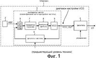
Фиг.1 (предшествующий уровень техники) является схемой одного примера местного генератора (гетеродина) 1. Радиоприемники и радиопередатчики, используемые, например, в сотовых телефонах, часто вмещают в себя множество подобных гетеродинов. Гетеродин этого типа обычно вмещает в себя источник 2 опорного тактового сигнала, схему 3 фазовой автоподстройки частоты и делитель 4 частоты. В проиллюстрированном примере фазовый детектор 5 принимает опорный тактовый сигнал REF от источника 2 опорного тактового сигнала, а также принимает сигнал обратной связи от делителя 6 частоты. Фазовый детектор 5 выводит сигнал фазовой ошибки, который подается на генератор 7 подкачки. Выходной сигнал генератора 7 подкачки фильтруется контурным фильтром 8, чтобы сформировать сигнал уровня напряжения. Сигнал уровня напряжения подается на управляющий входной вывод управляемого напряжением генератора (VCO) 9. Напряжение на управляющем входном выводе VCO 9 определяет частоту сигнала VCO_OUT, выводимого из VCO 9. Делитель 6 частоты делит частоту сигнала VCO_OUT и подает результирующий сигнал с разделенной частотой на фазовый детектор 5 в качестве сигнала обратной связи. Когда схема фазовой автоподстройки частоты синхронизирована, сигнал обратной связи и сигнал REF находятся в фазе, и частота сигнала VCO_OUT определяется коэффициентом деления, на которое делит делитель 6 частоты. Частота сигнала VCO_OUT представляет собой произведение коэффициента деления и частоты опорного тактового сигнала REF. Сигнал VCO_OUT обычно не выводится как выходной сигнал гетеродина (LO), а чаще сигнал VCO_OUT представляет собой сигнал с частотой, разделенной до более низкой частоты вторым делителем 4 частоты. Делитель 4 частоты может быть установлен, например, чтобы делить частоту на относительно малое целое число, например на два, или на четыре, или на восемь.Figure 1 (prior art) is a diagram of one example of a local generator (local oscillator) 1. Radio receivers and radio transmitters used, for example, in cell phones, often accommodate many such local oscillators. A local oscillator of this type typically contains a reference
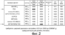
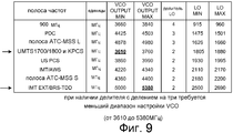
В случае интегральных схем приемопередатчика, интегрированных внутрь сотовых телефонов, часто бывает желательно сделать интегральную схему приемопередатчика такой, чтобы одна и та же конструкция интегральной схемы могла использоваться для связи в любой из множества различных полос частот. На Фиг.2 (предшествующий уровень техники) показаны примеры различных полос частот, по которым отдельному приемнику (в пределах интегральной схемы приемопередатчика сотового телефона) могло бы требоваться осуществлять связь. Крайние правые два столбца на Фиг.2 указывают выходные частоты сигналов гетеродина (LO), которые необходимо формировать. Столбец, обозначенный "LO DIVIDER" указывает число, на которое делит делитель 4 частоты. Два столбца, обозначенные "VCO OUTPUT MIN" и "VCO OUTPUT MAX", отображают соответствующие выходные частоты VCO, необходимые для формирования желаемых частот LO MIN и LO MAX, учитывая заданный в столбце LO DIVIDER коэффициент деления. Следует отметить, что для формирования требуемых выходных сигналов гетеродина с желаемыми частотами частота выходного сигнала VCO должна быть настраиваемой в пределах диапазона от 2950 мегагерц до 5380 мегагерц. Это относительно широкий диапазон настройки VCO. Может оказаться затруднительным реализовать VCO с широким диапазоном настройки, или, по другим причинам, может быть нежелательно предоставлять такой широкий диапазон настройки VCO.In the case of transceiver integrated circuits integrated within cell phones, it is often desirable to make the transceiver integrated circuit such that the same integrated circuit design can be used for communication in any of a variety of different frequency bands. Figure 2 (prior art) shows examples of various frequency bands over which an individual receiver (within the integrated circuit of a cell phone transceiver) might need to communicate. The rightmost two columns in FIG. 2 indicate the output frequencies of the local oscillator (LO) signals that need to be generated. The column marked "LO DIVIDER" indicates the number by which the
Если делитель 4 частоты мог бы быть установлен на деление на три, то можно было бы уменьшить диапазон настройки VCO. Хотя делители частоты, которые делят частоту на три, известны, такие делители частоты обычно не используются, поскольку желаемый выходной сигнал гетеродина часто фактически представляет собой не только один сигнал (LO), а чаще пару сигналов, причем фаза одного из сигналов не совпадает на девяносто градусов относительно других сигналов. Такие сигналы LO называются как квадратурные сигналы, или, как принято говорить, сигнал гетеродина находится "в квадратуре". Символы I и Q часто используются для обозначения таких квадратурных сигналов. Квадратурные сигналы могут быть, например, затребованы другой схемой приемника, чтобы выполнить модуляцию фазовым сдвигом и/или выполнить подавление зеркальных помех.If the
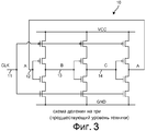
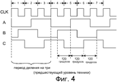
Фиг.3 (предшествующий уровень техники) является примером делителя 10 частоты с делением на три предшествующего уровня техники, изложенного в 1973 г. в статье, озаглавленной "Потребление малой мощности и высокая частота", Electronics Letters, Issue 17, vol. 9, August 23, 1973, авторы H. Oguey и C. Vittoz. Фиг.4 (предшествующий уровень техники) является временной диаграммой сигналов, иллюстрирующей работу схемы. Когда входной тактовый сигнал CLK частоты 3F подается на входной вывод 11, схема формирует три сигнала A, B и C на узлах 12, 13 и 14, соответственно, с частотой F. Никакие два из сигналов A, B и C не отличаются друг от друга на девяносто градусов, и делитель частоты не используется для делителя 4 частоты в гетеродине 1 на Фиг.1, если должны быть сформированы квадратурные выходные сигналы гетеродина.Figure 3 (prior art) is an example of a
СУЩНОСТЬ ИЗОБРЕТЕНИЯSUMMARY OF THE INVENTION
Гетеродин включает в себя программируемый делитель частоты, соединенный с выходом управляемого напряжением генератора (VCO). Программируемый делитель частоты может быть установлен на деление на три. Независимо от числа, на которое делит программируемый делитель частоты, программируемый делитель частоты выводит квадратурные сигналы (I, Q) с коэффициентом заполнения пятьдесят процентов, которые отличаются друг от друга по фазе на девяносто градусов. Чтобы делить на три, делитель частоты включает в себя делитель частоты с делением на три. Делитель частоты с делением на три включает в себя схему деления на три, схему задержки, и схему обратной связи. Схема деления частоты на три делит входной сигнал, принятый от VCO, и формирует из него три сигнала C, A' и B, которые отличаются друг от друга по фазе на сто двадцать градусов. Схема задержки задерживает второй сигнал A', чтобы сформировать задержанную версию A второго сигнала. Схема обратной связи управляет схемой задержки так, чтобы задержанная версия A не совпадала по фазе на девяносто градусов относительно первого сигнала C. Задержанная версия A может быть использована как квадратурный сигнал I, а первый сигнал C может быть использован как квадратурный сигнал Q. Контур обратной связи автоматически корректирует изменения и/или вариации в работе схемы вследствие температурных изменений, изменений питающего напряжения и/или вариаций в технологической обработке полупроводника.The local oscillator includes a programmable frequency divider connected to the output of a voltage controlled oscillator (VCO). The programmable frequency divider can be set to divide by three. Regardless of the number by which the programmable frequency divider divides, the programmable frequency divider outputs quadrature signals (I, Q) with a duty cycle of fifty percent, which differ in phase by ninety degrees. To divide by three, the frequency divider includes a frequency divider divided by three. The frequency divider with a division by three includes a division scheme by three, a delay circuit, and a feedback circuit. The frequency division circuit by three divides the input signal received from VCO and generates from it three signals C, A 'and B, which differ from each other in phase by one hundred and twenty degrees. The delay circuit delays the second signal A ′ to form a delayed version A of the second signal. The feedback circuit controls the delay circuit so that the delayed version A is not ninety degrees out of phase with respect to the first signal C. The delayed version A can be used as a quadrature signal I, and the first signal C can be used as a quadrature signal Q. Feedback loop automatically corrects changes and / or variations in the operation of the circuit due to temperature changes, changes in the supply voltage and / or variations in the processing of the semiconductor.
Программируемый делитель частоты может быть реализован в интегральной схеме RF приемопередатчика внутри сотового телефона. Исполняемые процессором команды в цифровой интегральной схеме основной полосы частот могут устанавливать коэффициент деления, на который программируемый делитель частоты делит, посредством передачи соответствующей управляющей информации через шину от цифровой интегральной схемы основной полосы частот на интегральную схему RF приемопередатчика.A programmable frequency divider can be implemented in an RF integrated circuit transceiver inside a cell phone. The processor-executed instructions in the digital integrated circuit of the main frequency band can set the division factor by which the programmable frequency divider divides by transmitting the corresponding control information via the bus from the digital integrated circuit of the main frequency band to the RF integrated circuit of the transceiver.
В одном конкретном примере схема обратной связи включает в себя участок цифровой логики и участок схемы усреднения и сравнения. Участок цифровой логики принимает сигналы A и C и формирует цифровой сигнал, указывающий величину времени T1 между первым фронтом сигнала A и фронтом сигнала C. Участок цифровой логики формирует также цифровой сигнал, указывающий величину времени T2 между фронтом сигнала C и вторым фронтом сигнала A. Цифровой сигнал, указывающий величину времени T1, преобразуется в сигнал уровня напряжения, указывающий величину времени T1. Цифровой сигнал, указывающий величину времени T2, преобразуется в сигнал уровня напряжения, указывающий величину времени T2. Сигналы двух уровней напряжения подаются на входы операционного усилителя так, что операционный усилитель формирует сигнал управления. Сигнал управления преобразуется в сигнал управления напряжения смещения, который подается на схему задержки. Через этот контур обратной связи схема обратной связи работает для управления задержкой схемы задержки так, чтобы разность фаз между сигналом C и сигналом A составляла девяносто градусов.In one specific example, the feedback circuit includes a digital logic portion and a portion of the averaging and comparison circuit. The digital logic section receives signals A and C and generates a digital signal indicating the amount of time T1 between the first edge of signal A and the edge of signal C. The digital logic section also generates a digital signal indicating the amount of time T2 between the edge of signal C and the second edge of signal A. Digital a signal indicating a time value T1 is converted to a voltage level signal indicating a time value T1. A digital signal indicating the amount of time T2 is converted to a voltage level signal indicating the amount of time T2. The signals of two voltage levels are fed to the inputs of the operational amplifier so that the operational amplifier generates a control signal. The control signal is converted to a bias voltage control signal, which is supplied to the delay circuit. Through this feedback loop, a feedback circuit works to control the delay of the delay circuit so that the phase difference between signal C and signal A is ninety degrees.
Выше было дано краткое изложение сущности изобретения, и оно неизбежно содержит упрощения, обобщения и исключения подробностей; следовательно, специалистам в данной области техники должно быть очевидно, что это краткое изложение служит только иллюстративным целям и не предполагает каких-либо ограничений. Другие аспекты, признаки изобретения и преимущества описываемых здесь устройств и/или процессов, определяемые исключительно в соответствии с формулой, станут очевидными из приведенного не ограничивающего подробного описания.Above was a brief summary of the invention, and it inevitably contains simplifications, generalizations and exclusions of details; therefore, it should be apparent to those skilled in the art that this summary is for illustrative purposes only and does not imply any limitations. Other aspects, features of the invention and advantages of the devices and / or processes described herein, determined solely in accordance with the claims, will become apparent from the non-limiting detailed description given.
КРАТКОЕ ОПИСАНИЕ ЧЕРТЕЖЕЙBRIEF DESCRIPTION OF THE DRAWINGS
Фиг.1 (предшествующий уровень техники) является схемой одного примера гетеродина, пригодного для использования в сотовом телефоне.Figure 1 (prior art) is a diagram of one example local oscillator suitable for use in a cell phone.
Фиг.2 (предшествующий уровень техники) - таблица, иллюстрирующая, что VCO гетеродина на Фиг.1 имеет нежелательно широкий диапазон настройки VCO.Figure 2 (prior art) is a table illustrating that the VCO of the local oscillator in Figure 1 has an undesirably wide range of VCO settings.
Фиг.3 (предшествующий уровень техники) - схема делителя частоты с делением на три предшествующего уровня техники.Figure 3 (prior art) is a diagram of a frequency divider divided by three prior art.
Фиг.4 (предшествующий уровень техники) - временная диаграмма сигналов, иллюстрирующая работу схемы делителя частоты с делением на три на Фиг.3 предшествующего уровня техники.Figure 4 (prior art) is a timing diagram of signals illustrating the operation of a frequency divider circuit divided by three in Figure 3 of the prior art.
Фиг.5 - блок-схема высокого уровня устройства 100 мобильной связи в соответствии с одним новым аспектом.5 is a high level block diagram of a mobile communication device 100 in accordance with one new aspect.
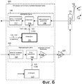
Фиг.6 - более подробная блок-схема интегральной схемы 103 RF приемопередатчика на Фиг.5.FIG. 6 is a more detailed block diagram of an RF transceiver integrated
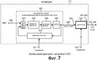
Фиг.7 - более подробная схема гетеродина 111 на Фиг.6.Fig.7 is a more detailed diagram of the
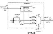
Фиг.8 - более подробная схема программируемого делителя 202 частоты гетеродина 111 на Фиг.7.Fig. 8 is a more detailed diagram of a
Фиг.9 - таблица, иллюстрирующая, что VCO гетеродина 111 на Фиг.7 имеет более узкий диапазон настройки VCO, чем схема VCO на Фиг.1 предшествующего уровня техники.Fig. 9 is a table illustrating that the VCO of the
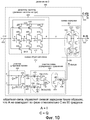
Фиг.10 - принципиальная схема нового делителя 300 частоты с делением на три из Фиг.8.Figure 10 is a schematic diagram of a
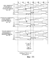
Фиг.11 - временная диаграмма сигналов, иллюстрирующая работу нового делителя 300 частоты с делением на три из Фиг.10.11 is a timing diagram of signals illustrating the operation of the
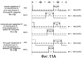
Фиг.11А - временная диаграмма сигналов, иллюстрирующая, как сигналы A&Cb и A&C преобразуются в соответствующие сигналы A&Cb (AVE) и A&C (AVE) уровня напряжения.11A is a timing diagram of signals illustrating how A & Cb and A&C signals are converted to respective voltage level signals A & Cb (AVE) and A&C (AVE).
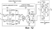
Фиг.12 - принципиальная схема другого варианта реализации схемы 402 обратной связи и схемы 401 задержки делителя 300 частоты с делением на три из Фиг.10.12 is a schematic diagram of another embodiment of a
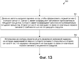
Фиг.13 - блок-схема последовательности операций способа 500 в соответствии с одним новым аспектом.13 is a flowchart of a
ПОДРОБНОЕ ОПИСАНИЕDETAILED DESCRIPTION
На Фиг.5 показана очень упрощенная блок-схема высокого уровня одного устройства 100 мобильной связи конкретного типа в соответствии с одним новым аспектом. В этом конкретном примере устройство 100 мобильной связи представляет собой 3G сотовый телефон, пригодный для работы или в соответствии с протоколом сотовой телефонной связи Множественного доступа с кодовым разделением каналов (CDMA), или в соответствии с протоколом сотовой телефонной связи GSM (Глобальная Система Мобильной Связи). Мобильный телефон включает в себя (среди некоторых других частей, не проиллюстрированных) антенну 102 и две интегральные схемы 103 и 104. Интегральную схему 104 называют "цифровой интегральной схемой основной полосы частот" или "интегральной схемой процессора основной полосы частот". Цифровая интегральная схема 104 основной полосы частот включает в себя, среди других частей, не проиллюстрированных, цифровой процессор 105, который исполняет команды, сохраняемые в процессорно-читаемом носителе 106. Процессор 105 может инициировать обмен информацией по шине 107, и интерфейсу 108A шины, и проводникам 109 шины, и в интерфейс 108B шины интегральной схемы 103. Интегральная схема 103 представляет собой интегральную схему RF приемопередатчика. Интегральную схему 103 RF приемопередатчика называют "приемопередатчиком", поскольку она включает в себя и передатчик, и приемник.5 shows a very simplified high-level block diagram of one particular type of mobile communication device 100 in accordance with one new aspect. In this specific example, the mobile communication device 100 is a 3G cell phone suitable for use either in accordance with a code division multiple access (CDMA) cellular telephone protocol or in accordance with a GSM cellular telephone protocol (Global System for Mobile Communications) . A mobile phone includes (among some other parts not illustrated) an
Фиг.6 является более подробной блок-схемой интегральной схемы 103 RF приемопередатчика из Фиг.5. Приемник включает в себя так называемую "приемную цепь" 110, а также гетеродин 111. Когда сотовый телефон принимает, высокочастотный сигнал 112 RF принимается антенной 102. Информация от сигнала 112 проходит через дуплексер 113 в приемную цепь 110. Сигнал 112 усиливается малошумящим усилителем (LNA) 115 и преобразуется с понижением частоты смесителем 116. Результирующий преобразованный с понижением частоты сигнал фильтруется фильтром 117 основной полосы частот и проходит на цифровую интегральную схему 104 основной полосы частот. Аналого-цифровой преобразователь 118 в цифровой интегральной схеме 104 основной полосы частот преобразует сигнал в цифровую форму, и результирующая цифровая информация обрабатывается цифровой схемой в цифровой интегральной схеме 104 основной полосы частот. Цифровая интегральная схема 104 основной полосы частот настраивает приемник, управляя частотой квадратурных сигналов I и Q гетеродина, подаваемых гетеродином 111 на смеситель 116 по проводникам 127 и 128.FIG. 6 is a more detailed block diagram of an RF transceiver integrated
Если сотовый телефон передает, то информация, которая должна быть передана, преобразуется в аналоговую форму цифроаналоговым преобразователем 119 в цифровой интегральной схеме 104 основной полосы частот и подается на "передающую цепь" 120. Фильтр 121 основной полосы частот отфильтровывает шум, обусловленный процессом цифроаналогового преобразования. Блок 122 смесителя под управлением гетеродина 123 затем преобразует сигнал с повышением частоты в высокочастотный сигнал. Предусилитель 124 и внешний усилитель 125 мощности усиливают высокочастотный сигнал для возбуждения антенны 102 так, чтобы высокочастотный RF сигнал 126 передавался антенной 102. Цифровая интегральная схема 104 основной полосы частот настраивает передатчик, управляя частотой квадратурных сигналов I и Q гетеродина, подаваемых гетеродином 123 на смеситель 122. Стрелка 130 представляет собой передачу информации от цифровой интегральной схемы 104 основной полосы частот через интерфейс 108A шины, по проводникам 109 шины, через интерфейс 108B шины, и через проводники 131 и 132 на гетеродин 111, чтобы установить коэффициент деления, на который делит делитель частоты в пределах гетеродина 111, как подробнее объясняется ниже.If the cell phone is transmitting, then the information to be transmitted is converted into analog form by a digital-to-analog converter 119 in the digital baseband integrated circuit 104 and supplied to the “transmitting circuit” 120. The
На Фиг.7 показана более подробная схема гетеродина 111. Гетеродин 111 включает в себя источник 200 опорного тактового сигнала (обозначенный здесь посредством проводника), синтезатор 201 частоты, и новый программируемый делитель 202 частоты. Синтезатор 201 частоты в приведенном примере является аналогом схемы фазовой автоподстройки частоты (PLL), которая включает в себя фазовый детектор 203, генератор 204 подкачки, контурный фильтр 205, управляемый напряжением генератор (VCO) 206 и делитель 207 частоты. Приемник приемной цепи 110 настраивается установкой частоты выходных квадратурных сигналов I и Q гетеродина на проводниках 127 и 128, соответственно. Частота квадратурных сигналов I и Q определяется коэффициентом деления, на который делитель 207 частоты делит, и коэффициентом деления, на который делит программируемый делитель 202 частоты. Частота опорного тактового сигнала REF фиксирована. Коэффициент деления, на который делит делитель 207 частоты, устанавливается значением, подаваемым на проводники 131 управления. Коэффициент деления, на который делит делитель 202 частоты, устанавливается значением, подаваемым на проводники 132 управления. В этом примере цифровая интегральная схема 104 основной полосы частот из Фиг.5 управляет этими значениями коэффициента деления через шину 109.7 shows a more detailed diagram of the
На Фиг.8 показана более подробная схема нового программируемого делителя 202 частоты из Фиг.7. Программируемый делитель 202 частоты включает в себя новый делитель 300 частоты с делением на три, делитель 301 пульсаций, и схему 302 мультиплексирования. Сигнал VCO_OUT от VCO 206 принимается через проводник 208 на входной вывод 303 делителя 202 частоты. Делитель 301 пульсаций представляет собой двоичный делитель, который имеет несколько каскадов. Первый каскад выводит набор квадратурных сигналов, которые имеют частоту в половину частоты сигнала VCO_OUT. Эти сигналы обозначены как DIV2 на Фиг.8. Второй каскад выводит набор квадратурных сигналов, которые имеют частоту в одну четверть частоты сигнала VCO_OUT. Эти сигналы обозначены как DIV4 на Фиг.8. Новый делитель 300 частоты с делением на три делит частоту сигнала VCO_OUT на три и выводит набор квадратурных сигналов, частота которых составляет одну треть частоты VCO_OUT. Эти сигналы обозначены как DIV3 на Фиг.8. То, какой из трех наборов квадратурных сигналов выводится из делителя 202 частоты на выходные выводы 304 и 305, определяется цифровым значением на проводниках 132 управления. Хотя символ мультиплексора проиллюстрирован как представляющий функцию мультиплексирования, использование мультиплексора не необходимо. В одном примере три выходных I проводника от блоков 300 и 301 соединены вместе, и три выходных Q проводника от блоков 300 и 301 соединены вместе. Управляющее значение на проводнике 132 управления позволяет соответствующему одному из блоков 300 и 301 управлять соответствующим набором I и Q сигналов на выходных выводах 304 и 305. Каждый из выходных выводов 304 и 305 служит, поэтому, своего рода выводом проводной схемы ИЛИ.On Fig shows a more detailed diagram of the new
На Фиг.9 показана таблица, иллюстрирующая преимущество, реализованное новым делителем 202 частоты. Делитель 202 частоты может делить частоту или на два, или на три, или на четыре. Для всех трех коэффициентов деления делитель 202 частоты выводит квадратурные сигналы I и Q. Следует отметить, что в таблице на Фиг.9 показаны те же самые полосы частот и те же самые частоты "LO MIN" и "LO MAX", что и в таблице на Фиг.2 предшествующего уровня техники, но следует отметить, что в таблице на Фиг.9 столбец "LO DIVIDER" указывает, что VCO_OUT является частотой, разделенной на три в двух случаях. В результате, диапазон настройки VCO уменьшается от широкого диапазона на Фиг.2 до более узкого диапазона перестройки от 3610 до 5380 мегагерц для случая на Фиг.9. Установка частоты VCO_OUT и установка значения "LO DIVIDER", при каждой ситуации рабочей полосы частот, управляются процессором 105 цифровой интегральной схемы 104 основной полосы частот, как объяснено выше. В одном преимущественном аспекте частота сигнала VCO_OUT и коэффициент деления, на который делит делитель 202 частоты, устанавливаются так, чтобы синтезатор 201 частоты мог быть такого типа, который имеет относительно узкий диапазон настройки VCO.9 is a table illustrating an advantage realized by the
На Фиг.10 показана более подробная схема одного варианта осуществления нового делителя 300 частоты с делением на три из Фиг.8. Делитель 300 частоты включает в себя делитель 400 частоты с делением на три, схему задержки 401 и схему обратной связи 402. Схема 402 обратной связи, в свою очередь, включает в себя участок 403 цифровой логики и участок 404 схемы усреднения и сравнения.Figure 10 shows a more detailed diagram of one embodiment of a
В одном примере делитель 400 частоты представляет собой делитель частоты, проиллюстрированный выше на Фиг.3. Делитель 400 частоты включает в себя двенадцать полевых транзисторов (FET) 405-416, составляющих три каскада, как проиллюстрировано. Первый каскад вмещает в себя первый P-канальный FET полевой транзистор (PFET) 405, второй PFET 407, первый N-канальный полевой транзистор (NFET) 406, и второй NFET 408. Затворы PFET 405 и NFET 406 подключены между собой, и стоки PFET 405 и NFET 406 подключены между собой. Сток второго PFET 407 соединяется с истоком первого PFET 405, и сток второго NFET 408 соединяется с истоком первого NFET 406. Исток второго PFET 407 подключен с шиной 416 подачи напряжения, и исток второго NFET 408 подключен с земляной шиной 417. Второй и третий каскады транзисторов соединяются между собой подобным образом. Когда входной тактовый сигнал CLK с частотой 3F (VCO_OUT) подается на входной вывод 418, делитель 400 частоты формирует три сигнала C, A' и B на узлах 419, 420 и 421, соответственно. Каждый из этих сигналов имеет коэффициент заполнения приблизительно пятьдесят процентов. Второй сигнал A' не совпадает по фазе относительно первого сигнала C приблизительно на 120 градусов, и третий сигнал B не совпадает по фазе относительно второго сигнала А' приблизительно на 120 градусов, и первый сигнал C не совпадает по фазе относительно третьего сигнала B приблизительно на 120 градусов.In one example, the
Первый сигнал C на узле 419 подается на выходной вывод 422 как квадратурный сигнал Q. Второй сигнал A' подается на схему 401 задержки. Схема 401 задержки формирует задержанную версию A второго сигнала A', пропуская второй сигнал через пару инвертирующих схем 423 и 424. Схема 401 задержки выводит результирующую задержанную версию A на выходной вывод 425 как квадратурный сигнал I.The first signal C at
Схема обратной связи 402 работает, чтобы управлять задержкой через схему 401 задержки так, чтобы сигнал на выходном выводе 425 не совпадал по фазе на девяносто градусов относительно сигнала C на выходном выводе 422. Участок 403 цифровой логики включает в себя первый логический элемент 426 И, который формирует цифровой сигнал на узле 427, который указывает величину времени Т1 между первым передним фронтом задержанной версии A второго сигнала и следующим передним фронтом первого сигнала C. Участок 403 цифровой логики включает в себя второй логический элемент 428 И, который формирует цифровой сигнал на узле 429, который указывает величину времени T2 между передним фронтом первого сигнала C и вторым задним фронтом задержанной версии A второго сигнала. Первый передний фронт задержанной версии A второго сигнала и второй задний фронт задержанной версии A второго сигнала определяют период высокого уровня импульсов задержанной версии A (длительность, когда задержанная версия A имеет высокий цифровой логический уровень).
В примере на Фиг.10, если периоды Т1 и T2 времени равны, то сигналы I и Q на выходных выводах 425 и 422 не будут совпадать по фазе друг относительно друга на девяносто градусов. Участок 404 схемы усреднения и сравнения имеет первый RC-фильтр 430 нижних частот, и второй RC-фильтр 431 нижних частот. Первый RC-фильтр 430 нижних частот грубо преобразует сигнал на узле 427 в соответствующий сигнал уровня напряжения на узле 432. Уровень напряжения на узле 432 указывает время Т1. Подобным образом, второй RC-фильтр 431 нижних частот грубо преобразует сигнал на узле 429 в соответствующий сигнал уровня напряжения на узле 433. Уровень напряжения на узле 433 указывает время T2. Операционный усилитель 434 принимает сигналы на узлах 432 и 433 на своих не инвертирующем и инвертирующем входных выводах, соответственно, и выводит сигнал управления. Сигнал управления преобразуется схемой 435 смещения в соответствующее напряжение смещения VBIASN, которое смещает транзисторы 436 и 437 схемы 401 задержки. Чем выше напряжение смещения VBIASN, подаваемое на затворы транзисторов 436 и 437, тем меньше потребляемый инвертирующими схемами 423 и 424 ток, и тем быстрее инвертирующие схемы 423 и 424 будут в состоянии переключать свои выходы. Соответственно, чем выше напряжение смещения VBIASN, тем меньше задержка при прохождении через схему 401 задержки.In the example of FIG. 10, if the time periods T1 and T2 are equal, then the signals I and Q at the
Схема 438 предоставлена, чтобы добавить полюс на соответствующей частоте, чтобы препятствовать колебаниям контура управления. Если напряжение на узле 432 выше, чем напряжение на узле 433, то Т1 оказывается больше, чем T2, и управляющее напряжение на узле 439 уменьшается, чтобы увеличить задержку через схему 401 задержки так, чтобы сделать Т1 и T2 более равными. Если, с другой стороны, напряжение на узле 432 ниже, чем напряжение на узле 433, то Т1 оказывается меньше, чем T2, и управляющее напряжение на узле 439 увеличивается, чтобы уменьшить задержку через схему 401 задержки так, чтобы сделать Т1 и T2 более равными. Работа контура управления обратной связи такова, что Т1 и T2 управляются до их равенства, и такова, чтобы разность фаз между сигналами C и A составляла девяносто градусов.
Работа схемы на Фиг.10 дополнительно поясняется применительно к временной диаграмме сигналов на Фиг.11. Временная диаграмма сигналов на Фиг.11 фактически включает в себя три набора сигналов. Верхний набор диаграмм сигналов представляет собой ситуацию, в которой Т1 больше, чем T2. Средний набор диаграмм сигналов представляет собой ситуацию, в которой Т1 и T2 равны. Нижний набор диаграмм сигналов представляет собой ситуацию, в которой Т1 меньше, чем T2. Как можно видеть из диаграмм сигналов на Фиг.11, время Т1 представляет собой время, когда сигнал A&Cb имеет высокий цифровой логический уровень. Сигнал A&Cb - это сигнал, присутствующий на узле 427 на Фиг.10. Сигнал A&Cb формируется инвертированием первого сигнала C, чтобы сформировать инвертированную версию Cb сигнала C. Символ "b" в этом обозначении означает "инвертирование". Элемент И 426 выполняет логическую операцию И сигнала Cb и сигнала A. Обозначение "A&Cb" означает логическую операцию И сигналов "A" и "Cb". Таким же образом, время T2 представляет собой время, когда сигнал A&Cb имеет высокий цифровой логический уровень. Сигнал A&C - это сигнал, присутствующий на узле 429 на Фиг.10. Элемент И 428 выполняет логическую операцию И сигнала C и сигнала A. Обозначение "A&C" означает логическую операцию И сигналов "A" и "C".The operation of the circuit of FIG. 10 is further explained with reference to the timing diagram of the signals of FIG. 11. The signal timing diagram of FIG. 11 actually includes three sets of signals. The top set of waveform diagrams is a situation in which T1 is greater than T2. The average set of signal diagrams is a situation in which T1 and T2 are equal. The bottom set of waveform diagrams is a situation in which T1 is less than T2. As can be seen from the signal diagrams of FIG. 11, the time T1 is the time when the signal A & Cb has a high digital logic level. The signal A & Cb is a signal present at the
На Фиг.11А проиллюстрировано, как сигналы A&Cb и A&C на узлах 427 и 429 преобразуются в соответствующие сигналы A&Cb (AVE) и A&C (AVE) уровня напряжения на узлах 432 и 433, соответственно. Сигналы A&Cb (AVE), и A&C (AVE) уровня напряжения представлены на Фиг.11А горизонтальными пунктирными линиями. Чем больше доля времени, когда сигнал, поданный на вход RC-фильтра нижних частот, имеет высокий уровень, тем больше доля времени, когда конденсатор RC-фильтра нижних частот будет заряжаться, и тем меньше доля времени, когда конденсатор будет разряжаться. Соответственно, чем больше доля времени, когда сигнал, поданный на вход RC-фильтра нижних частот, имеет высокий уровень, тем выше уровень сигнала напряжения, выходящего из RC-фильтра нижних частот.11A illustrates how the signals A & Cb and A&C at
Хотя один вариант реализации нового делителя 300 частоты с делением на три приведен на Фиг.10, имеются и другие варианты. На Фиг.12 приведен пример, в котором участок 403 цифровой логики формирует четыре цифровых сигнала Ab&Cb, A&C, A&Cb и Ab&C. Хотя операционный усилитель 434 на Фиг.10 выводит несимметричный сигнал управления так, что один сигнал VBIASN управления напряжением смещения управляет задержкой прохождения через схему 401 задержки, в примере на Фиг.12 операционный усилитель 434 выводит пару дифференциальных сигналов на соответствующую пару схем 435 и 435A смещения. Схема 435A смещения имеет связанную с ней схему 438A, чтобы добавить полюс для предотвращения колебаний контура управления. Одна схема 435 смещения выводит напряжение VBIASN смещения на затвор NFET 436. Вторая схема 435A смещения выводит напряжение VBIASP смещения на затвор PFET 436A. В примере схемы 401 задержки на Фиг.12 вторая инвертирующая схема 424 схемы 401 задержки представляет собой простой инвертор и вмещает в себя только два транзистора, как проиллюстрировано. Схема 402 обратной связи работает, изменяя задержку прохождения через схему 401 задержки, изменяя проводимость NFET 436 и PFET 436A.Although one embodiment of the
На Фиг.13 показана блок-схема последовательности операций способа 500 в соответствии с одним новым аспектом. На первом этапе входной сигнал (например, VCO_OUT) имеет разделенную на три частоту (этап 501), чтобы сформировать первый сигнал C и второй сигнал А'. Первый сигнал C имеет коэффициент заполнения приблизительно пятьдесят процентов, и второй сигнал A' имеет коэффициент заполнения приблизительно пятьдесят процентов. Второй сигнал A' не совпадает по фазе относительно первого сигнала C приблизительно на сто двадцать градусов.13 is a flowchart of a
На втором этапе используется контур управления (этап 502), чтобы управлять величиной задержки, посредством которой задержанная версия A второго сигнала A' задерживается относительно второго сигнала A' так, что задержанная версия A второго сигнала не совпадает по фазе относительно первого сигнала C на девяносто градусов. В одном примере способа задержанная версия A второго сигнала и первого сигнала C используются как выходные сигналы гетеродина (квадратурные сигналы I и Q) в радиопередатчике и/или приемнике сотового телефона, и частота входного сигнала составляет, по меньшей мере, сто мегагерц.In a second step, a control loop is used (step 502) to control the amount of delay by which the delayed version A of the second signal A 'is delayed relative to the second signal A' so that the delayed version A of the second signal is not ninety degrees in phase with respect to the first signal C . In one example of the method, the delayed version A of the second signal and the first signal C is used as the local oscillator output signals (quadrature signals I and Q) in the radio transmitter and / or receiver of the cell phone, and the frequency of the input signal is at least one hundred megahertz.
В одном или более примерных вариантах реализации описанные функции могут быть осуществлены в аппаратном обеспечении, программном обеспечении, встроенном программном обеспечении, или в любой их комбинации. Если они осуществляются в программном обеспечении, функции могут быть сохранены, или переданы на компьютерно-читаемый или процессорно-читаемый носитель как одна или более команд или код. Компьютерно-читаемый и процессорно-читаемый носители включают в себя и компьютерные носители данных, и среду передачи, включая в себя любую среду, которая способствует переносу программы из одного места в другое. Носитель данных может быть любым доступным носителем, к которому может осуществлять доступ компьютер или процессор. В качестве не ограничивающего примера, такой носитель может содержать RAM, ROM, EEPROM, CD-ROM или другой оптический дисковый накопитель, магнитный дисковый накопитель или другие магнитные устройства хранения, или любой другой носитель, который может быть использован для переноса или хранения желаемого программного кода в виде команд или структур данных, и к которому может осуществлять доступ компьютер или процессор. Кроме того, подключение также следует называть компьютерно-читаемым носителем. Например, если программное обеспечение передается с веб-сайта, сервера, или другого удаленного источника с использованием коаксиального кабеля, оптоволоконного кабеля, витой пары, цифровой абонентской линии (DSL), или беспроводной технологии, например инфракрасной, радио, и микроволновой, то подключение коаксиальным кабелем, оптоволоконным кабелем, витой парой, DSL, или с помощью беспроводных технологий, например инфракрасной, радио, и микроволновой, включено в определение носителя. Используемые в данном документе понятия оптический диск и магнитный диск включают в себя компакт-диск (CD), лазерный диск, оптический диск, цифровой универсальный диск (DVD), гибкий диск и blu-ray диск, причем магнитные диски обычно воспроизводят данные магнитным образом, а оптические диски воспроизводят данные оптическим образом с помощью лазеров. Комбинации всего вышеупомянутого также должны быть включены в объем компьютерно-читаемых носителей. Исполнение процессором 105 набора команд, сохраняемых в процессорно-читаемом носителе 106 цифровой ИС 104 основной полосы частот, в некоторых вариантах реализации инициирует передачу цифровой информации от цифровой ИС 104 основной полосы частот через проводники 109 шины на новый делитель 202 частоты из Фиг.7, и новый делитель 202 частоты выполнен так, чтобы делить частоту на три и выводить пару квадратурных сигналов (I и Q), фазы которых различаются на девяносто градусов. Когда делитель 202 частоты установлен таким образом, сигнал VCO_OUT имеет частоту 3F, и квадратурные сигналы представляют собой сигналы частотой F с коэффициентом заполнения пятьдесят процентов.In one or more exemplary embodiments, the described functions may be implemented in hardware, software, firmware, or any combination thereof. If implemented in software, the functions may be stored, or transferred to a computer-readable or processor-readable medium as one or more instructions or code. Computer-readable and processor-readable media include both computer storage media and a transmission medium, including any medium that facilitates transferring a program from one place to another. The storage medium may be any available medium that can be accessed by a computer or processor. By way of non-limiting example, such a medium may comprise RAM, ROM, EEPROM, CD-ROM or other optical disk drive, magnetic disk drive or other magnetic storage devices, or any other medium that can be used to transfer or store the desired program code in the form of instructions or data structures, and which can be accessed by a computer or processor. In addition, the connection should also be called computer-readable medium. For example, if the software is transferred from a website, server, or other remote source using a coaxial cable, fiber optic cable, twisted pair cable, digital subscriber line (DSL), or wireless technology such as infrared, radio, and microwave, then the connection is coaxial cable, fiber optic cable, twisted pair cable, DSL, or using wireless technologies such as infrared, radio, and microwave, is included in the media definition. As used herein, the concepts of an optical disk and a magnetic disk include a compact disk (CD), a laser disk, an optical disk, a digital versatile disk (DVD), a floppy disk, and a blu-ray disk, with magnetic disks typically reproducing data in a magnetic manner, and optical discs reproduce data optically with lasers. Combinations of all of the above should also be included within the scope of computer-readable media. Execution by the processor 105 of a set of instructions stored in a processor-readable medium 106 of the digital baseband IC 104, in some embodiments, initiates the transmission of digital information from the digital baseband IC 104 via bus conductors 109 to the
Хотя определенные варианты реализации описаны выше в иллюстративных целях, принципы данного патентного документа общеприменимы и не ограничиваются описанными выше конкретными вариантами реализации. Схема 402 обратной связи может быть использована, чтобы выполнить квадратурные делители частоты, которые делят на коэффициенты деления, не равные 2N (N - целое число). Например, квадратурный делитель частоты, имеющий коэффициент деления 1,5, может быть осуществлен с применением удвоителя частоты, следующего за квадратурным делителем частоты с делением на три, описанным выше. Выходные сигналы I и Q делителя частоты с делением на три могут быть сигналами с коэффициентом заполнения двадцать пять процентов или сигналами с коэффициентом заполнения пятьдесят процентов. Соответственно, различные модификации, адаптации, и комбинации различных признаков описанных конкретных вариантов реализации могут быть осуществлены без отступления от объема представленной ниже формулы.Although certain embodiments have been described above for illustrative purposes, the principles of this patent document are generally applicable and are not limited to the specific embodiments described above.
Claims (32)
схему задержки, которая принимает второй сигнал А' и выводит задержанную версию А второго сигнала; и схему обратной связи, которая управляет схемой задержки так, чтобы задержанная версия А второго сигнала не совпадала по фазе относительно первого сигнала С на девяносто градусов.7. A frequency division circuit divided by three, comprising: a frequency divider that receives an input signal with a frequency of 3F and outputs a first signal C with a frequency F, and outputs a second signal A 'with a frequency F, wherein the first signal C has a duty cycle of about fifty percent, and wherein the second signal A ′ has a duty cycle of about fifty percent, the second signal A ′ not in phase relative to the first signal C by about one hundred and twenty degrees;
a delay circuit that receives the second signal A ′ and outputs a delayed version A of the second signal; and a feedback circuit that controls the delay circuit so that the delayed version A of the second signal does not phase out from the first signal C by ninety degrees.
средство для формирования третьего сигнала, указывающего величину времени Т1 между первым фронтом задержанной версии А второго сигнала и фронтом первого сигнала С; и средство для формирования четвертого сигнала, указывающего величину времени Т2 между фронтом первого сигнала С и вторым фронтом задержанной версии А второго сигнала.31. The circuit of claim 27, wherein said means for controlling the amount of delay A further comprises:
means for generating a third signal indicating the amount of time T1 between the first front of the delayed version A of the second signal and the front of the first signal C; and means for generating a fourth signal indicating the amount of time T2 between the front of the first signal C and the second front of the delayed version A of the second signal.
Applications Claiming Priority (3)
| Application Number | Priority Date | Filing Date | Title |
|---|---|---|---|
| US12/193,693 | 2008-08-18 | ||
| US12/193,693 US7825703B2 (en) | 2008-08-18 | 2008-08-18 | Divide-by-three quadrature frequency divider |
| PCT/US2009/054211 WO2010022092A1 (en) | 2008-08-18 | 2009-08-18 | Divide-by-three quadrature frequency divider |
Publications (2)
| Publication Number | Publication Date |
|---|---|
| RU2011110168A RU2011110168A (en) | 2012-09-27 |
| RU2479121C2 true RU2479121C2 (en) | 2013-04-10 |
Family
ID=41170029
Family Applications (1)
| Application Number | Title | Priority Date | Filing Date |
|---|---|---|---|
| RU2011110168/08A RU2479121C2 (en) | 2008-08-18 | 2009-08-18 | Quadrature frequency divider with division by three |
Country Status (11)
| Country | Link |
|---|---|
| US (1) | US7825703B2 (en) |
| EP (2) | EP2797234B1 (en) |
| JP (1) | JP5259823B2 (en) |
| KR (1) | KR101246962B1 (en) |
| CN (2) | CN102124653B (en) |
| BR (1) | BRPI0917342A2 (en) |
| CA (1) | CA2735676C (en) |
| IN (1) | IN2014CN03747A (en) |
| RU (1) | RU2479121C2 (en) |
| TW (1) | TW201015859A (en) |
| WO (1) | WO2010022092A1 (en) |
Cited By (2)
| Publication number | Priority date | Publication date | Assignee | Title |
|---|---|---|---|---|
| RU2648614C1 (en) * | 2015-01-09 | 2018-03-26 | Шэньчжэнь Чайна Стар Оптоэлектроникс Текнолоджи Ко., Лтд. | Scan exciting circuit and the nand logical operation circuit of such circuit |
| RU2752485C1 (en) * | 2020-12-03 | 2021-07-28 | Акционерное общество "ПКК МИЛАНДР" | Frequency divider with variable division coefficient |
Families Citing this family (22)
| Publication number | Priority date | Publication date | Assignee | Title |
|---|---|---|---|---|
| US8344765B2 (en) * | 2009-07-16 | 2013-01-01 | Qualcomm, Incorporated | Frequency divider with a configurable dividing ratio |
| WO2012050761A2 (en) * | 2010-09-30 | 2012-04-19 | Dow Corning Corporation | Process for preparing an acryloyloxysilane |
| US8768994B2 (en) * | 2010-10-22 | 2014-07-01 | Taiwan Semiconductor Manufacturing Company, Ltd. | Filter auto-calibration using multi-clock generator |
| KR101292767B1 (en) * | 2011-09-06 | 2013-08-02 | 동국대학교 산학협력단 | Pass transistor and odd number frequency devider with 50% duty cycle including it |
| US8803568B2 (en) * | 2011-11-28 | 2014-08-12 | Qualcomm Incorporated | Dividing a frequency by 1.5 to produce a quadrature signal |
| US9065449B2 (en) * | 2013-10-28 | 2015-06-23 | Avago Technologies General Ip (Singapore) Pte. Ltd. | High-speed divide-by-1.5 circuit with 50 percent duty cycle |
| CN104734695B (en) | 2013-12-24 | 2018-05-04 | 澜起科技(上海)有限公司 | Signal generator, electronic system and the method for producing signal |
| US9455716B2 (en) | 2014-05-28 | 2016-09-27 | Qualcomm Incorporated | Reconfigurable fractional divider |
| CN105391444B (en) | 2014-09-04 | 2018-07-20 | 中芯国际集成电路制造(上海)有限公司 | A kind of frequency dividing circuit and electronic device |
| US20160079985A1 (en) * | 2014-09-16 | 2016-03-17 | Qualcomm Incorporated | Quadrature local oscillator phase synthesis and architecture for divide-by-odd-number frequency dividers |
| US9705664B2 (en) | 2015-06-18 | 2017-07-11 | Mediatek Singapore Pte. Ltd. | Synthesizer module, RF transceiver and method therefor |
| US10164574B2 (en) | 2015-07-07 | 2018-12-25 | Mediatek Inc. | Method for generating a plurality of oscillating signals with different phases and associated circuit and local oscillator |
| US9973182B2 (en) * | 2016-09-14 | 2018-05-15 | Qualcomm Incorporated | Re-timing based clock generation and residual sideband (RSB) enhancement circuit |
| US10374588B2 (en) | 2016-10-31 | 2019-08-06 | Mediatek Inc. | Quadrature clock generating mechanism of communication system transmitter |
| US10116290B1 (en) * | 2017-12-07 | 2018-10-30 | Speedlink Technology Inc. | RF frontend having a wideband mm wave frequency doubler |
| CN113348627A (en) * | 2019-01-31 | 2021-09-03 | 华为技术有限公司 | Buffer circuit, frequency division circuit and communication equipment |
| US10454462B1 (en) * | 2019-04-18 | 2019-10-22 | Hong Kong Applied Science and Technology Research Institute Company Limited | 50% duty cycle quadrature-in and quadrature-out (QIQO) divide-by-3 circuit |
| US11646919B2 (en) * | 2020-01-08 | 2023-05-09 | Mediatek Singapore Pte. Ltd. | IQ generator for mixer |
| US11264995B1 (en) * | 2020-10-26 | 2022-03-01 | Qualcomm Incorporated | System and method for maintaining local oscillator (LO) phase continuity |
| CN112787659A (en) * | 2020-12-30 | 2021-05-11 | 瑞声科技(南京)有限公司 | Three-frequency divider circuit |
| CN112994682B (en) * | 2021-05-10 | 2021-08-03 | 上海灵动微电子股份有限公司 | Clock frequency divider, microcontroller and phase-locked loop circuit based on switched capacitor |
| CN115149943B (en) * | 2022-08-31 | 2022-11-22 | 上海韬润半导体有限公司 | Frequency dividing circuit |
Citations (2)
| Publication number | Priority date | Publication date | Assignee | Title |
|---|---|---|---|---|
| RU2273860C2 (en) * | 2004-04-12 | 2006-04-10 | федеральное государственное унитарное предприятие "Государственный Рязанский приборный завод" (ФГУП ГРПЗ) | Coherent receiver of a radiolocation station with a digital arrangement for amplitude and phase adjusting of quadrature component of a receiving signal |
| RU70059U1 (en) * | 2007-08-13 | 2008-01-10 | Открытое акционерное общество "Концерн "Созвездие" | DIGITAL FREQUENCY SYNTHESIS |
Family Cites Families (12)
| Publication number | Priority date | Publication date | Assignee | Title |
|---|---|---|---|---|
| US4366394A (en) * | 1980-09-25 | 1982-12-28 | Rockwell International Corporation | Divide by three clock divider with symmetrical output |
| US4399326A (en) * | 1981-01-12 | 1983-08-16 | Bode Harald E W | Audio signal processing system |
| GB9727244D0 (en) | 1997-12-23 | 1998-02-25 | Sgs Thomson Microelectronics | A dividing circuit and transistor stage therefor |
| JP2002026726A (en) * | 2000-07-07 | 2002-01-25 | Mitsubishi Electric Corp | Semiconductor integrated circuit |
| US6389095B1 (en) * | 2000-10-27 | 2002-05-14 | Qualcomm, Incorporated | Divide-by-three circuit |
| US6960962B2 (en) * | 2001-01-12 | 2005-11-01 | Qualcomm Inc. | Local oscillator leakage control in direct conversion processes |
| EP1606881A1 (en) | 2003-03-19 | 2005-12-21 | Koninklijke Philips Electronics N.V. | Quadrature clock divider |
| NO323203B1 (en) * | 2004-09-24 | 2007-01-22 | Texas Instr Norway As | Quadrature parts-by-three frequency parts |
| JP4687082B2 (en) * | 2004-11-30 | 2011-05-25 | セイコーエプソン株式会社 | Electronic device and wireless communication terminal |
| US7123103B1 (en) | 2005-03-31 | 2006-10-17 | Conexant Systems, Inc. | Systems and method for automatic quadrature phase imbalance compensation using a delay locked loop |
| JP2009017528A (en) * | 2007-06-05 | 2009-01-22 | Seiko Epson Corp | Pulse generating circuit and uwb communication system |
| JP4675422B2 (en) * | 2009-03-30 | 2011-04-20 | 日本電信電話株式会社 | Wireless transmitter |
-
2008
- 2008-08-18 US US12/193,693 patent/US7825703B2/en active Active
-
2009
- 2009-08-18 IN IN3747CHN2014 patent/IN2014CN03747A/en unknown
- 2009-08-18 JP JP2011523943A patent/JP5259823B2/en not_active Expired - Fee Related
- 2009-08-18 CA CA2735676A patent/CA2735676C/en not_active Expired - Fee Related
- 2009-08-18 EP EP14175067.9A patent/EP2797234B1/en active Active
- 2009-08-18 TW TW098127743A patent/TW201015859A/en unknown
- 2009-08-18 RU RU2011110168/08A patent/RU2479121C2/en not_active IP Right Cessation
- 2009-08-18 EP EP09791628.2A patent/EP2327159B1/en active Active
- 2009-08-18 CN CN200980131897.9A patent/CN102124653B/en active Active
- 2009-08-18 CN CN201410195693.4A patent/CN103944564B/en active Active
- 2009-08-18 WO PCT/US2009/054211 patent/WO2010022092A1/en active Application Filing
- 2009-08-18 BR BRPI0917342A patent/BRPI0917342A2/en not_active Application Discontinuation
- 2009-08-18 KR KR1020117006247A patent/KR101246962B1/en active IP Right Grant
Patent Citations (2)
| Publication number | Priority date | Publication date | Assignee | Title |
|---|---|---|---|---|
| RU2273860C2 (en) * | 2004-04-12 | 2006-04-10 | федеральное государственное унитарное предприятие "Государственный Рязанский приборный завод" (ФГУП ГРПЗ) | Coherent receiver of a radiolocation station with a digital arrangement for amplitude and phase adjusting of quadrature component of a receiving signal |
| RU70059U1 (en) * | 2007-08-13 | 2008-01-10 | Открытое акционерное общество "Концерн "Созвездие" | DIGITAL FREQUENCY SYNTHESIS |
Cited By (2)
| Publication number | Priority date | Publication date | Assignee | Title |
|---|---|---|---|---|
| RU2648614C1 (en) * | 2015-01-09 | 2018-03-26 | Шэньчжэнь Чайна Стар Оптоэлектроникс Текнолоджи Ко., Лтд. | Scan exciting circuit and the nand logical operation circuit of such circuit |
| RU2752485C1 (en) * | 2020-12-03 | 2021-07-28 | Акционерное общество "ПКК МИЛАНДР" | Frequency divider with variable division coefficient |
Also Published As
| Publication number | Publication date |
|---|---|
| IN2014CN03747A (en) | 2015-09-25 |
| CN102124653B (en) | 2014-10-08 |
| TW201015859A (en) | 2010-04-16 |
| US20100039153A1 (en) | 2010-02-18 |
| RU2011110168A (en) | 2012-09-27 |
| CN103944564A (en) | 2014-07-23 |
| JP2012500596A (en) | 2012-01-05 |
| JP5259823B2 (en) | 2013-08-07 |
| US7825703B2 (en) | 2010-11-02 |
| CA2735676C (en) | 2014-09-16 |
| EP2327159A1 (en) | 2011-06-01 |
| EP2797234A1 (en) | 2014-10-29 |
| EP2797234B1 (en) | 2018-12-26 |
| WO2010022092A1 (en) | 2010-02-25 |
| EP2327159B1 (en) | 2015-01-14 |
| BRPI0917342A2 (en) | 2015-11-17 |
| CN103944564B (en) | 2017-08-25 |
| KR20110055663A (en) | 2011-05-25 |
| EP2797234A8 (en) | 2014-12-03 |
| KR101246962B1 (en) | 2013-03-25 |
| CA2735676A1 (en) | 2010-02-25 |
| CN102124653A (en) | 2011-07-13 |
Similar Documents
| Publication | Publication Date | Title |
|---|---|---|
| RU2479121C2 (en) | Quadrature frequency divider with division by three | |
| US9160396B2 (en) | LO generation and distribution in a multi-band transceiver | |
| US9154143B2 (en) | Semiconductor device | |
| US7180375B2 (en) | PLL circuit | |
| KR20110027773A (en) | Dithering a digitally-controlled oscillator output in a phase-locked loop | |
| US8374283B2 (en) | Local oscillator with injection pulling suppression and spurious products filtering | |
| US7911281B2 (en) | PLL circuit and radio communication apparatus | |
| Yu et al. | A Single-Chip 125-MHz to 32-GHz Signal Source in 0.18-$\mu $ m SiGe BiCMOS | |
| KR20160101974A (en) | Local oscillator signal generation using delay locked loops | |
| US7639088B2 (en) | Phase-locked loop start-up techniques | |
| US6825729B2 (en) | Frequency synthesizer with sigma-delta modulation | |
| JP2001127554A (en) | Voltage controlled oscillator | |
| US9088285B2 (en) | Dynamic divider having interlocking circuit | |
| CN116781071A (en) | Control method of fractional frequency division phase-locked loop system and fractional frequency division phase-locked loop system | |
| JP2000165277A (en) | Local oscillation circuit |
Legal Events
| Date | Code | Title | Description |
|---|---|---|---|
| MM4A | The patent is invalid due to non-payment of fees |
Effective date: 20190819 |