RU2433503C1 - Method of hidden fault location of silicon-gate mos multiplexers - Google Patents
Method of hidden fault location of silicon-gate mos multiplexers Download PDFInfo
- Publication number
- RU2433503C1 RU2433503C1 RU2010129098/28A RU2010129098A RU2433503C1 RU 2433503 C1 RU2433503 C1 RU 2433503C1 RU 2010129098/28 A RU2010129098/28 A RU 2010129098/28A RU 2010129098 A RU2010129098 A RU 2010129098A RU 2433503 C1 RU2433503 C1 RU 2433503C1
- Authority
- RU
- Russia
- Prior art keywords
- mos
- indium
- substrate
- sources
- multiplexers
- Prior art date
Links
- 238000000034 method Methods 0.000 title claims abstract description 13
- 229910052738 indium Inorganic materials 0.000 claims abstract description 26
- APFVFJFRJDLVQX-UHFFFAOYSA-N indium atom Chemical compound [In] APFVFJFRJDLVQX-UHFFFAOYSA-N 0.000 claims abstract description 24
- 239000000758 substrate Substances 0.000 claims abstract description 18
- 239000013078 crystal Substances 0.000 claims abstract description 10
- 229910052710 silicon Inorganic materials 0.000 claims abstract description 6
- 239000010703 silicon Substances 0.000 claims abstract description 6
- XUIMIQQOPSSXEZ-UHFFFAOYSA-N Silicon Chemical compound [Si] XUIMIQQOPSSXEZ-UHFFFAOYSA-N 0.000 claims abstract description 3
- 230000007547 defect Effects 0.000 claims description 12
- 230000001681 protective effect Effects 0.000 claims description 3
- 238000001514 detection method Methods 0.000 claims description 2
- 230000015572 biosynthetic process Effects 0.000 claims 1
- 239000011248 coating agent Substances 0.000 abstract 1
- 238000000576 coating method Methods 0.000 abstract 1
- 230000005611 electricity Effects 0.000 abstract 1
- 230000008030 elimination Effects 0.000 abstract 1
- 238000003379 elimination reaction Methods 0.000 abstract 1
- 239000000126 substance Substances 0.000 abstract 1
- 239000010410 layer Substances 0.000 description 16
- 238000004519 manufacturing process Methods 0.000 description 3
- 239000011159 matrix material Substances 0.000 description 2
- 238000003032 molecular docking Methods 0.000 description 2
- 238000012544 monitoring process Methods 0.000 description 2
- 238000000206 photolithography Methods 0.000 description 2
- 239000011148 porous material Substances 0.000 description 1
- 239000011241 protective layer Substances 0.000 description 1
- 239000007921 spray Substances 0.000 description 1
Images
Landscapes
- Testing Or Measuring Of Semiconductors Or The Like (AREA)
Abstract
Description
Изобретение относится к технологии изготовления и способам тестирования МОП мультиплексоров.The invention relates to manufacturing techniques and methods for testing MOS multiplexers.
В настоящее время широко используется способ изготовления гибридных ИК матричных фотоприемных устройств (МФПУ) методом перевернутого монтажа фоточувствительных элементов с МОП мультиплексором при помощи индиевых столбиков. После стыковки часто обнаруживаются электрические дефекты МОП мультиплексора, определить которые без специальных мер тестирования до стыковки невозможно, например электрическое короткое замыкание между входными контактами и выходными шинами МОП мультиплексора (исток - шина стока ключевого МОП транзистора) в ячейке матрицы считывания фотосигнала.Currently, a widely used method for the manufacture of hybrid IR matrix photodetectors (MFP) by the method of inverted mounting of photosensitive elements with a MOS multiplexer using indium columns. After docking, electrical defects of the MOS multiplexer are often detected, which it is impossible to determine without special testing measures before docking, for example, an electric short circuit between the input contacts and output buses of the MOS multiplexer (the source is the drain bus of the key MOS transistor) in the cell of the photo readout matrix.
Известно, что для выявления упомянутого выше дефекта используется сплошной слой In толщиной не менее толщины окисного слоя, закорачивающий все истоки МОП транзисторов слоем индия на подложку [RU, патент на изобретение №2388110 С1]. Путь тока при этом: стоковая шина-дефект-исток-слой индия-подложка.It is known that to identify the aforementioned defect, a continuous In layer is used with a thickness not less than the thickness of the oxide layer, shorting all the sources of MOS transistors with an indium layer on a substrate [RU, patent for invention No. 2388110 C1]. The current path in this case is: stock bus-defect-source-layer indium-substrate.
Указанный метод обнаружения дефектов имеет следующие недостатки: наличие слоя индия над металлизированными шинами стоков может приводить к их закоротке на подложку слоем индия напрямую через дефект (пору) в защитном окисле над стоком, миную область истока, что можно назвать «ложной тревогой», так как в рабочей структуре слоя индия над стоковыми шинами нет. Путь тока в этом случае: стоковая шина-дефект-слой индия-подложка.The indicated method for detecting defects has the following disadvantages: the presence of an indium layer over metallized runoff tires can lead to their shorting to the substrate with an indium layer directly through a defect (pore) in the protective oxide above the runoff, the minimum area of the source, which can be called a “false alarm”, since there is no indium layer over the stock tires in the working structure. The current path in this case is: stock bus-defect-layer indium-substrate.
Задачей изобретения является увеличение надежности (достоверности) метода обнаружения скрытых дефектов кремниевых МОП мультиплексоров за счет исключения прямых закороток стоковых областей на подложку путем формирования в каждом кристалле МОП мультиплексора слоя индия в виде полос только над истоками МОП транзисторов.The objective of the invention is to increase the reliability (reliability) of the method for detecting latent defects of silicon MOS multiplexers by eliminating direct short-circuits of the drain areas on the substrate by forming an indium layer in the form of stripes in each crystal of the MOS multiplexer only above the sources of MOS transistors.
Технический результат достигается тем, что:The technical result is achieved by the fact that:
- на металлизированные площадки истоков, вскрытые в окисле, наносят слой индия толщиной, равной необходимой высоте In столбика;- a layer of indium with a thickness equal to the necessary height In of the column is deposited on the metallized sites of the sources opened in the oxide;
- при помощи фотолитографической обработки формируют в каждом кристалле область индия в виде полос, которые располагаются только над истоками МОП транзисторов и закорачивают их на подложку;- using photolithographic processing, an indium region is formed in each crystal in the form of bands that are located only above the sources of MOS transistors and short-circuit them on a substrate;
- контролируют функционирование мультиплексоров и фиксируют наличие дефектов, в том числе и электрические закоротки исток-сток, которые не проявлялись при контроле функционирования без индия;- they control the functioning of multiplexers and fix the presence of defects, including the source-drain electrical short circuits, which did not appear during operation monitoring without indium;
- далее методом фотолитографии формируют индиевые столбики высотой, равной толщине напыленной пленки индия.- then, using photolithography, indium columns are formed with a height equal to the thickness of the deposited indium film.
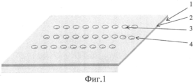
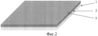
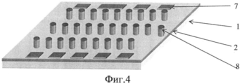
Последовательность технологической цепочки предлагаемого способа иллюстрируется на фиг.1-4, где:The sequence of the technological chain of the proposed method is illustrated in figures 1-4, where:
1 - годный кристалл МОП мультиплексора, являющийся частью пластины;1 - suitable crystal MOS multiplexer, which is part of the plate;
2 - слой защитного окисла;2 - a layer of protective oxide;
3 - контактные окна к металлизированным площадкам истоков МОП транзисторов;3 - contact windows to the metallized sites of the sources of MOS transistors;
4 - контактное окно к подложке;4 - contact window to the substrate;
5 - слой индия;5 - layer of indium;
6 - область индия в виде полос, сформированная только над истоками МОП транзисторов мультиплексора и закорачивающая их на подложку;6 - indium region in the form of stripes, formed only above the sources of MOS transistors of the multiplexer and shorting them to the substrate;
7 - контактные площадки для контроля функционирования МОП мультиплексора;7 - contact pads for monitoring the operation of the MOS multiplexer;
8 - индиевые столбики.8 - indium columns.
Способ обнаружения скрытых дефектов МОП мультиплексоров осуществляется в следующей последовательности:A method for detecting latent defects of MOS multiplexers is carried out in the following sequence:
- на кремниевой пластине с годными кристаллами МОП мультиплексоров вскрывают окна в защитном слое окисла к металлизированным площадкам истоков МОП транзисторов и подложке (фиг.1);- on a silicon wafer with suitable crystals of MOS multiplexers open the windows in the protective layer of oxide to the metallized areas of the sources of MOS transistors and the substrate (figure 1);
- напыляют слой индия толщиной, равной необходимой высоте In столбиков (фиг.2);- spray a layer of indium with a thickness equal to the required height In columns (figure 2);
- проводят фотолитографическую обработку по слою индия для получения области индия в виде полос, расположенных только над истоками МОП транзисторов, которая закорачивает все истоки МОП транзисторов на подложку (фиг.3);- carry out photolithographic processing on the indium layer to obtain the indium region in the form of bands located only above the sources of MOS transistors, which shorts all the sources of MOS transistors on the substrate (figure 3);
- проводят контроль функционирования годных МОП мультиплексоров с выявлением скрытых дефектов - закороток исток-сток;- they monitor the functioning of suitable MOS multiplexers with the identification of hidden defects - short-circuit source-drain;
- проводят фотолитографическую обработку по слою индия для формирования столбиков, режут пластину на кристаллы, осуществляют травление индия для формирования столбиков (фиг.4).- conduct photolithographic processing on a layer of indium to form columns, cut the plate into crystals, etch indium to form columns (figure 4).
Предлагаемый способ обнаружения дефектов гармонично вписывается в технологию изготовления МОП мультиплексоров.The proposed method for detecting defects harmoniously fits into the manufacturing technology of MOS multiplexers.
Изготовлены экспериментальные образцы кремниевых МОП мультиплексоров с проведением тестирования на предмет обнаружения скрытых дефектов методом закорачивания истоков МОП транзисторов на подложку слоем индия с рельефом 3…4 мкм и с последующей фотолитографией для получения однородных столбиков высотой 9…10 мкм.Experimental samples of silicon MOS multiplexers were made with testing for the detection of latent defects by shorting the sources of MOS transistors onto a substrate with an indium layer with a relief of 3 ... 4 μm and subsequent photolithography to obtain uniform columns 9 ... 10 μm high.
Claims (1)
Priority Applications (1)
| Application Number | Priority Date | Filing Date | Title |
|---|---|---|---|
| RU2010129098/28A RU2433503C1 (en) | 2010-07-13 | 2010-07-13 | Method of hidden fault location of silicon-gate mos multiplexers |
Applications Claiming Priority (1)
| Application Number | Priority Date | Filing Date | Title |
|---|---|---|---|
| RU2010129098/28A RU2433503C1 (en) | 2010-07-13 | 2010-07-13 | Method of hidden fault location of silicon-gate mos multiplexers |
Publications (1)
| Publication Number | Publication Date |
|---|---|
| RU2433503C1 true RU2433503C1 (en) | 2011-11-10 |
Family
ID=44997363
Family Applications (1)
| Application Number | Title | Priority Date | Filing Date |
|---|---|---|---|
| RU2010129098/28A RU2433503C1 (en) | 2010-07-13 | 2010-07-13 | Method of hidden fault location of silicon-gate mos multiplexers |
Country Status (1)
| Country | Link |
|---|---|
| RU (1) | RU2433503C1 (en) |
Cited By (1)
| Publication number | Priority date | Publication date | Assignee | Title |
|---|---|---|---|---|
| RU2523752C1 (en) * | 2013-04-01 | 2014-07-20 | Российская Федерация, От Имени Которой Выступает Министерство Промышленности И Торговли Российской Федерации | Method of detecting hidden defects on lsi reading arrays |
Citations (4)
| Publication number | Priority date | Publication date | Assignee | Title |
|---|---|---|---|---|
| RU2005308C1 (en) * | 1991-01-09 | 1993-12-30 | Московский Инженерно-Физический Институт | Method of accelerated testing of mos integrated microcircuits on plate |
| RU2073254C1 (en) * | 1993-06-25 | 1997-02-10 | Московский Инженерно-Физический Институт | Semiconductor devices and integral circuit plates testing method |
| US6275059B1 (en) * | 1997-04-04 | 2001-08-14 | University Of Florida | Method for testing and diagnosing MOS transistors |
| RU2388110C1 (en) * | 2009-02-19 | 2010-04-27 | Федеральное государственное унитарное предприятие "НПО "ОРИОН" | Method of detecting hidden defects in matrix or linear mos multiplexers |
-
2010
- 2010-07-13 RU RU2010129098/28A patent/RU2433503C1/en active IP Right Revival
Patent Citations (4)
| Publication number | Priority date | Publication date | Assignee | Title |
|---|---|---|---|---|
| RU2005308C1 (en) * | 1991-01-09 | 1993-12-30 | Московский Инженерно-Физический Институт | Method of accelerated testing of mos integrated microcircuits on plate |
| RU2073254C1 (en) * | 1993-06-25 | 1997-02-10 | Московский Инженерно-Физический Институт | Semiconductor devices and integral circuit plates testing method |
| US6275059B1 (en) * | 1997-04-04 | 2001-08-14 | University Of Florida | Method for testing and diagnosing MOS transistors |
| RU2388110C1 (en) * | 2009-02-19 | 2010-04-27 | Федеральное государственное унитарное предприятие "НПО "ОРИОН" | Method of detecting hidden defects in matrix or linear mos multiplexers |
Non-Patent Citations (1)
| Title |
|---|
| Low-Bias CTIA Multiplexer for 1024 Element InGaAs Line Sensors. Walter F. Kosonocky at all. SPIE, v.2226, 1994, p.152. * |
Cited By (1)
| Publication number | Priority date | Publication date | Assignee | Title |
|---|---|---|---|---|
| RU2523752C1 (en) * | 2013-04-01 | 2014-07-20 | Российская Федерация, От Имени Которой Выступает Министерство Промышленности И Торговли Российской Федерации | Method of detecting hidden defects on lsi reading arrays |
Similar Documents
| Publication | Publication Date | Title |
|---|---|---|
| US20100055809A1 (en) | Process of fabricating a workpiece using a test mask | |
| CN102629613B (en) | Method for manufacturing X-ray sensor | |
| CN103618499B (en) | A kind of solar battery sheet PID testing apparatus and method of testing | |
| KR20160143800A (en) | Array substrate and manufacturing method thereof, x-ray flat panel detector and camera system | |
| CN102664184A (en) | Array substrate of X ray detection device and manufacturing method thereof | |
| US9515118B2 (en) | Radiation detecting panel | |
| EP2856135B1 (en) | Sensor with integrated control device | |
| KR101428115B1 (en) | Array testing method using electric bias stress for tft array | |
| JP5923972B2 (en) | Method for manufacturing photoelectric conversion device and method for manufacturing imaging device using photoelectric conversion device | |
| US20130306873A1 (en) | Radiation detecting panel | |
| RU2415493C1 (en) | Method to detect hidden defects of matrix or linear silicon mos multiplexor | |
| RU2433503C1 (en) | Method of hidden fault location of silicon-gate mos multiplexers | |
| RU2388110C1 (en) | Method of detecting hidden defects in matrix or linear mos multiplexers | |
| US9588237B2 (en) | Digital X-ray detector and method for manufacturing the X-ray detector | |
| RU2474918C1 (en) | Method to detect hidden electric defects of matrix or linear silicon mos multiplexors | |
| US20110180716A1 (en) | Radiation detection element | |
| US20210272859A1 (en) | Array substrate and fabrication method thereof, and display device | |
| CN115565903B (en) | Electrical property detection method in packaging process | |
| EP2810058A1 (en) | Radiation detecting panel | |
| KR20150067830A (en) | Array substrate for X-ray Detector and Method of manufacturing the same | |
| TW506013B (en) | Etching method and apparatus for semiconductor device | |
| US20150177319A1 (en) | Integrated circuits with copper hillock-detecting structures and methods for detecting copper hillocks using the same | |
| CN107170765B (en) | A detection substrate and preparation method thereof, and X-ray detector | |
| CN110854092A (en) | Shared contact hole and its etching defect detection method | |
| WO2014081694A1 (en) | Detecting defects within photovoltaic modules |
Legal Events
| Date | Code | Title | Description |
|---|---|---|---|
| MM4A | The patent is invalid due to non-payment of fees |
Effective date: 20140714 |
|
| NF4A | Reinstatement of patent |
Effective date: 20160910 |