RU2359373C2 - Feed line of planar edge element - Google Patents
Feed line of planar edge element Download PDFInfo
- Publication number
- RU2359373C2 RU2359373C2 RU2006123262/09A RU2006123262A RU2359373C2 RU 2359373 C2 RU2359373 C2 RU 2359373C2 RU 2006123262/09 A RU2006123262/09 A RU 2006123262/09A RU 2006123262 A RU2006123262 A RU 2006123262A RU 2359373 C2 RU2359373 C2 RU 2359373C2
- Authority
- RU
- Russia
- Prior art keywords
- antenna
- metal sheet
- antenna device
- line
- supply
- Prior art date
Links
- 239000002184 metal Substances 0.000 claims abstract description 83
- 229910052751 metal Inorganic materials 0.000 claims abstract description 83
- 239000004020 conductor Substances 0.000 claims description 43
- 230000010287 polarization Effects 0.000 claims description 24
- 230000005540 biological transmission Effects 0.000 claims description 8
- 230000008878 coupling Effects 0.000 claims description 2
- 238000010168 coupling process Methods 0.000 claims description 2
- 238000005859 coupling reaction Methods 0.000 claims description 2
- 230000015572 biosynthetic process Effects 0.000 claims 1
- 230000000694 effects Effects 0.000 abstract description 2
- 239000000126 substance Substances 0.000 abstract 1
- 239000000758 substrate Substances 0.000 description 21
- 239000010410 layer Substances 0.000 description 17
- 230000009977 dual effect Effects 0.000 description 11
- 238000003491 array Methods 0.000 description 9
- RYGMFSIKBFXOCR-UHFFFAOYSA-N Copper Chemical compound [Cu] RYGMFSIKBFXOCR-UHFFFAOYSA-N 0.000 description 7
- 239000000463 material Substances 0.000 description 7
- 238000005476 soldering Methods 0.000 description 7
- 229910052802 copper Inorganic materials 0.000 description 6
- 239000010949 copper Substances 0.000 description 6
- 230000005284 excitation Effects 0.000 description 6
- 239000003989 dielectric material Substances 0.000 description 4
- 238000009826 distribution Methods 0.000 description 4
- 238000004519 manufacturing process Methods 0.000 description 4
- 238000005452 bending Methods 0.000 description 3
- -1 polytetrafluoroethylene Polymers 0.000 description 3
- 229920001343 polytetrafluoroethylene Polymers 0.000 description 3
- 239000004810 polytetrafluoroethylene Substances 0.000 description 3
- 230000005855 radiation Effects 0.000 description 3
- 238000009825 accumulation Methods 0.000 description 2
- 239000000853 adhesive Substances 0.000 description 2
- 238000004026 adhesive bonding Methods 0.000 description 2
- 230000001070 adhesive effect Effects 0.000 description 2
- 238000013459 approach Methods 0.000 description 2
- 238000001816 cooling Methods 0.000 description 2
- 238000005388 cross polarization Methods 0.000 description 2
- 238000005530 etching Methods 0.000 description 2
- 238000005562 fading Methods 0.000 description 2
- 239000011229 interlayer Substances 0.000 description 2
- 238000000034 method Methods 0.000 description 2
- 239000000203 mixture Substances 0.000 description 2
- 239000004033 plastic Substances 0.000 description 2
- 229920003023 plastic Polymers 0.000 description 2
- 230000007704 transition Effects 0.000 description 2
- 229920005830 Polyurethane Foam Polymers 0.000 description 1
- 230000006978 adaptation Effects 0.000 description 1
- 230000003321 amplification Effects 0.000 description 1
- 230000001413 cellular effect Effects 0.000 description 1
- 239000011248 coating agent Substances 0.000 description 1
- 238000000576 coating method Methods 0.000 description 1
- 238000010276 construction Methods 0.000 description 1
- 239000011889 copper foil Substances 0.000 description 1
- 238000005520 cutting process Methods 0.000 description 1
- 230000001419 dependent effect Effects 0.000 description 1
- 238000010586 diagram Methods 0.000 description 1
- 230000005684 electric field Effects 0.000 description 1
- 230000005672 electromagnetic field Effects 0.000 description 1
- 230000005670 electromagnetic radiation Effects 0.000 description 1
- 239000006260 foam Substances 0.000 description 1
- 238000003698 laser cutting Methods 0.000 description 1
- 238000003754 machining Methods 0.000 description 1
- 238000003199 nucleic acid amplification method Methods 0.000 description 1
- 238000005554 pickling Methods 0.000 description 1
- 239000011496 polyurethane foam Substances 0.000 description 1
- 238000004080 punching Methods 0.000 description 1
- 238000005096 rolling process Methods 0.000 description 1
- 238000007650 screen-printing Methods 0.000 description 1
- 239000002356 single layer Substances 0.000 description 1
- 230000003068 static effect Effects 0.000 description 1
- 230000001629 suppression Effects 0.000 description 1
- XLYOFNOQVPJJNP-UHFFFAOYSA-N water Substances O XLYOFNOQVPJJNP-UHFFFAOYSA-N 0.000 description 1
Images

Classifications
-
- H—ELECTRICITY
- H01—ELECTRIC ELEMENTS
- H01Q—ANTENNAS, i.e. RADIO AERIALS
- H01Q13/00—Waveguide horns or mouths; Slot antennas; Leaky-waveguide antennas; Equivalent structures causing radiation along the transmission path of a guided wave
- H01Q13/08—Radiating ends of two-conductor microwave transmission lines, e.g. of coaxial lines, of microstrip lines
- H01Q13/085—Slot-line radiating ends
-
- H—ELECTRICITY
- H01—ELECTRIC ELEMENTS
- H01Q—ANTENNAS, i.e. RADIO AERIALS
- H01Q21/00—Antenna arrays or systems
- H01Q21/06—Arrays of individually energised antenna units similarly polarised and spaced apart
- H01Q21/061—Two dimensional planar arrays
- H01Q21/064—Two dimensional planar arrays using horn or slot aerials
-
- H—ELECTRICITY
- H01—ELECTRIC ELEMENTS
- H01Q—ANTENNAS, i.e. RADIO AERIALS
- H01Q21/00—Antenna arrays or systems
- H01Q21/06—Arrays of individually energised antenna units similarly polarised and spaced apart
- H01Q21/061—Two dimensional planar arrays
- H01Q21/067—Two dimensional planar arrays using endfire radiating aerial units transverse to the plane of the array
-
- H—ELECTRICITY
- H01—ELECTRIC ELEMENTS
- H01Q—ANTENNAS, i.e. RADIO AERIALS
- H01Q21/00—Antenna arrays or systems
- H01Q21/24—Combinations of antenna units polarised in different directions for transmitting or receiving circularly and elliptically polarised waves or waves linearly polarised in any direction
Landscapes
- Variable-Direction Aerials And Aerial Arrays (AREA)
- Waveguide Aerials (AREA)
Abstract
Description
Область техникиTechnical field
Настоящее изобретение относится к широкополосному нерезонансному антенному устройству для беспроводной передачи информации с использованием электромагнитных сигналов, содержащему металлический листовой слой, образующий плоскость, с щелевой линией, которая содержит первую часть и вторую часть, причем сторона второй части, наиболее удаленная от первой части, переходит в расширяющуюся, имеющую открытый конец клиновидную щель в металлическом листовом слое.The present invention relates to a broadband non-resonant antenna device for wireless information transmission using electromagnetic signals, comprising a metal sheet layer forming a plane, with a slit line that contains the first part and the second part, the side of the second part farthest from the first part becomes an expanding wedge-shaped gap having an open end in a metal sheet layer.
Настоящее изобретение также относится к антенной решетке, содержащей множество упомянутых антенных устройств.The present invention also relates to an antenna array comprising a plurality of said antenna devices.
Предшествующий уровень техникиState of the art
В системах для беспроводной передачи информации с использованием электромагнитных сигналов, например в радиолокации и сотовой телефонии и в других областях телекоммуникаций, существует настоятельная потребность в эффективных антеннах, как в одиночных антеннах, так и в групповых антеннах или антенных решетках. Для различных применений требуются различные типы антенн с различными свойствами. Для многих применений требуются широкополосные свойства.In systems for the wireless transmission of information using electromagnetic signals, for example, in radar and cellular telephony and in other areas of telecommunications, there is an urgent need for efficient antennas, both for single antennas and for group antennas or antenna arrays. For various applications, different types of antennas with different properties are required. Many applications require broadband properties.
Когда антенный элемент используется в составе решетки, то есть когда некоторое количество антенных элементов расположено в горизонтальный ряд или вертикальный столбец, питание антенного элемента может осуществляться с переменной фазой, в результате чего главный лепесток диаграммы направленности антенной решетки может ориентироваться в различных направлениях вдоль антенной решетки. Может также использоваться и двухмерная антенная решетка, в которой некоторое количество антенных элементов расположено в горизонтальных рядах и вертикальных столбцах. Питание этих элементов в таком случае может осуществляться с переменной фазой вдоль как горизонтальных рядов, так и вертикальных столбцов, что делает возможным ориентировать главный лепесток диаграммы направленности антенной решетки в различных горизонтальных и вертикальных направлениях вдоль антенной решетки. Эти антенные решетки с управлением положением диаграммы направленности также именуются фазированными антенными решетками.When an antenna element is used as part of an array, that is, when a number of antenna elements are arranged in a horizontal row or vertical column, the antenna element can be supplied with a variable phase, as a result of which the main lobe of the antenna array can be oriented in different directions along the antenna array. A two-dimensional antenna array can also be used, in which a number of antenna elements are located in horizontal rows and vertical columns. The power of these elements in this case can be carried out with a variable phase along both horizontal rows and vertical columns, which makes it possible to orient the main lobe of the antenna array in various horizontal and vertical directions along the antenna array. These directional antenna arrays are also referred to as phased array antennas.
Антенные элементы могут также быть упорядочены в ортогонально расположенные пары, излучающие в ортогональных направлениях. Эти антенны называются антеннами с двойной поляризацией. Антенная решетка может таким образом иметь двойную поляризацию, если она состоит из равного количества ортогонально расположенных пар антенных элементов. Одна из причин для использования антенны с двойной поляризацией состоит в том, что требуется так называемое поляризационное разнесение. Поляризационное разнесение требуется, например, в случае, когда существует риск того, что сигнал антенны будет отражаться таким образом, что основной сигнал и отраженный сигнал будут иметь противоположные фазы в точке приема, вызывая глубокое замирание сигнала. Если используется две поляризации, то риск замирания снижается, поскольку обе поляризации должны были бы замирать в одно и то же время.Antenna elements can also be arranged in orthogonally spaced pairs radiating in orthogonal directions. These antennas are called dual polarized antennas. An antenna array can thus be double polarized if it consists of an equal number of orthogonally arranged pairs of antenna elements. One of the reasons for using a dual polarized antenna is that so-called polarization diversity is required. Polarization diversity is required, for example, when there is a risk that the antenna signal will be reflected in such a way that the main signal and the reflected signal will have opposite phases at the receiving point, causing a deep fading of the signal. If two polarizations are used, the risk of fading is reduced, since both polarizations would have to freeze at the same time.
Одним видом нерезонансного антенного элемента, который обычно используется, когда требуется работа в широкой полосе частот, то есть когда требуется работа в широком частотном диапазоне, является так называемая щелевая антенна, которая относится к виду так называемого элемента осевого излучения. Кроме того, при использовании в составе антенной решетки использование щелевых антенных элементов позволяет сформировать направление антенной решетки таким образом, чтобы сканировать в широком угловом диапазоне. Особо предпочтительным является использование антенного элемента с клиновидной щелью, выполненной в металлическом слое и расширяющейся по мере приближения к краю металлического слоя.One type of non-resonant antenna element, which is usually used when work is required in a wide frequency band, that is, when work is required in a wide frequency range, is the so-called slot antenna, which refers to the form of the so-called axial radiation element. In addition, when used in the composition of the antenna array, the use of slot antenna elements allows you to form the direction of the antenna array in such a way as to scan in a wide angular range. Particularly preferred is the use of an antenna element with a wedge-shaped slit made in the metal layer and expanding as it approaches the edge of the metal layer.
Одним специальным видом антенного элемента с клиновидной щелью является так называемый щелевой антенный элемент «Vivaldi», который может быть использован один или в составе антенной решетки.One special type of antenna element with a wedge-shaped slit is the so-called slotted antenna element "Vivaldi", which can be used alone or as part of an antenna array.
Типичный антенный элемент с клиновидной щелью может быть образован на первой покрытой медью подложке, например подложке на основе политетрафторэтилена, причем медь на одной стороне, являющейся питающей стороной, удалена травлением, за исключением единственной микрополосковой питающей линии. На другой стороне подложки в меди образована щель, расширяющаяся по мере приближения к краю подложки, образуя клиновидную щель. Эта клиновидность обычно представлена экспоненциальной формой. Микрополосковая питающая линия проходит к щели на другой стороне подложки таким образом, что продольная протяженность микрополосковой питающей линии, по сути, перпендикулярна продольной протяженности щели. Если питающая линия является незамкнутой, то микрополосковая питающая линия проходит приблизительно на расстоянии λg/4 от щели, то есть на одну четверть длины волны в материале, так называемой длины волны в волноводе. Незамкнутая питающая линия благодаря этой длине λg/4 трансформируется в коротко замкнутую под щелью питающую линию. В таком случае микрополосковая питающая линия ответвляет энергию в щель, поскольку электромагнитное поле микрополосковой питающей линии прерывается этой щелью.A typical wedge-shaped antenna element can be formed on a first copper-coated substrate, for example a polytetrafluoroethylene-based substrate, wherein copper on one side, which is the supply side, is removed by etching, with the exception of a single microstrip supply line. A gap is formed in the copper on the other side of the substrate, expanding as it approaches the edge of the substrate, forming a wedge-shaped gap. This wedge shape is usually represented by an exponential form. The microstrip supply line extends to the gap on the other side of the substrate in such a way that the longitudinal extent of the microstrip supply line is essentially perpendicular to the longitudinal length of the gap. If the feed line is open, then the microstrip feed line runs approximately at a distance of λ g / 4 from the slot, that is, one quarter of the wavelength in the material, the so-called wavelength in the waveguide. Due to this length λ g / 4, an open supply line is transformed into a supply line shortly closed under the slit. In this case, the microstrip supply line branches energy into the slot, since the electromagnetic field of the microstrip supply line is interrupted by this gap.
Однако эта конструкция является асимметричной, если смотреть на край слоистого листа, на котором сформирована клиновидная щель, поскольку на одной стороне этого слоистого листа располагается питающая линия, а на другой стороне - клиновидная щелевая структура. Эта асимметрия может вызывать кросс-поляризацию в диаграмме направленности антенны. Один из способов компенсации влияния асимметрии состоит в том, чтобы на первый слоистый лист поместить второй слоистый лист без меди на одной его стороне и с существенно идентичной клиновидной щелевой структурой на его другой стороне таким образом, чтобы сторона без меди на втором слоистом листе была обращена к стороне с микрополосковой питающей линией на первой подложке. Таким образом, питающая линия зажата между двумя слоистыми листами, образуя полосковую питающую линию, с существенно идентичными клиновидными щелями, вытравленными на медном покрытии на внешних сторонах, образующих двухстороннюю щелевую антенну.However, this design is asymmetric when looking at the edge of the laminate sheet on which the wedge-shaped slit is formed, since there is a supply line on one side of this laminated sheet and a wedge-shaped slotted structure on the other side. This asymmetry can cause cross-polarization in the antenna pattern. One way to compensate for the effect of asymmetry is to place a second copper-free laminate on one side of the first laminate and with a substantially identical wedge-shaped gap structure on its other side, so that the copper-free side on the second laminate is facing side with a microstrip supply line on the first substrate. Thus, the supply line is sandwiched between two layered sheets, forming a strip supply line, with substantially identical wedge-shaped slits etched on the copper coating on the outer sides, forming a two-sided slot antenna.
Базовая конфигурация антенного элемента с клиновидной щелью, относящегося к типу «Vivaldi», описана в статье «Wideband Vivaldi arrays for large aperture antennas» («Широкополосные антенные решетки «Vivaldi» для больших апертурных антенн»), авторы Daniel H. Shaubert (Дэниэл Шоберт) и Tan-Huat Chio (Тан-Хуат Чио). Здесь длина λg/4 реализована посредством так называемого радиального шлейфа для достижения бульшей ширины полосы частот. Другой конец щели, противоположный клиновидной части щели, оканчивается круговой частью, лишенной меди, образующей двумерный резонатор, в результате чего формируется незамкнутая щелевая линия вблизи точки возбуждения. В статье также описано, каким образом с использованием антенного элемента «Vivaldi» можно сформировать антенные решетки. Проблема с этой симметричной конструкцией антенного элемента «Vivaldi» состоит в том, что в материале подложки возникают так называемые моды параллельных пластин, то есть нежелательное распространение электромагнитного излучения. Для подавления этих мод параллельных пластин медные слои на внешних сторонах слоистых листов вокруг клиновидной щелевой структуры должны соединяться посредством металлических контактных столбиков, межслойных переходов.The basic configuration of a Vivaldi-type wedge-shaped antenna element is described in the article “Wideband Vivaldi arrays for large aperture antennas” by Daniel H. Shaubert (Daniel Schobert ) and Tan-Huat Chio (Tan-Huat Chio). Here, the length λ g / 4 is realized by a so-called radial loop to achieve a wider bandwidth. The other end of the slit, opposite the wedge-shaped part of the slit, ends in a circular part, deprived of copper, forming a two-dimensional resonator, as a result of which an open slot line is formed near the point of excitation. The article also describes how antenna arrays can be formed using the Vivaldi antenna element. The problem with this symmetrical design of the Vivaldi antenna element is that the so-called parallel plate modes, that is, the unwanted propagation of electromagnetic radiation, appear in the substrate material. To suppress these modes of parallel plates, copper layers on the outer sides of the laminated sheets around the wedge-shaped slit structure should be connected by means of metal contact posts, interlayer transitions.
Эта двухсторонняя антенна с клиновидной щелью, имеющая межслойные переходы для подавления мод, в конечном счете, приводит к довольно сложной структуре подложек, особенно в конструкции антенной решетки. Использование подложек вызывает диэлектрические потери, а также утяжеляет получаемую в результате антенну. Использование материалов подложек также невыгодно в случае, когда антенна предназначена для использования в космических приложениях, то есть на спутнике, поскольку накопление электростатических зарядов в пластмассовом материале может в результате привести к разрядам, которые могут оказаться губительными для расположенных рядом электронных схем. Кроме того, обычные подложки из политетрафторэтилена относительно дороги.This two-sided wedge-shaped antenna with interlayer transitions for mode suppression ultimately leads to a rather complex substrate structure, especially in the design of the antenna array. The use of substrates causes dielectric losses and also makes the resulting antenna heavier. The use of substrate materials is also disadvantageous when the antenna is intended for use in space applications, that is, on a satellite, since the accumulation of electrostatic charges in the plastic material can result in discharges that can be harmful to adjacent electronic circuits. In addition, conventional polytetrafluoroethylene substrates are relatively expensive.
US 5142255 описывает вытравленные на подложке, копланарные волноводные фильтры, которые могут быть объединены с щелевой антенной, которая запитывается активными компонентами. Это, однако, довольно узкополосная структура, поскольку копланарные волноводные фильтры являются резонансными для некоторых узких полос частот. Активные компоненты также могут оказывать влияние на ширину полосы частот этой структуры.US 5142255 describes etched on a substrate, coplanar waveguide filters, which can be combined with a slot antenna, which is fed by active components. However, this is a rather narrow-band structure, since coplanar waveguide filters are resonant for some narrow frequency bands. Active components can also affect the bandwidth of this structure.
Ни один из вышеназванных документов не раскрывает решение, в котором широкополосный симметричный антенный элемент с клиновидной щелью не поддерживался бы подложкой.None of the above documents discloses a solution in which a broadband symmetric antenna element with a wedge-shaped slit would not be supported by the substrate.
Сущность изобретенияSUMMARY OF THE INVENTION
Задача настоящего изобретения состоит в создании антенного устройства и способа его изготовления, посредством которых может быть решена вышеописанная проблема, в частности, антенного элемента с клиновидной щелью, который не должен поддерживаться подложкой и который, кроме того, является симметричным. Эта задача решается посредством антенного устройства вышеуказанного типа, причем устройство дополнительно содержит питающую линию в металлическом листовом слое, причем питающая линия содержит питающую часть с первым концом и вторым концом и зазоры, отделяющие питающую часть от окружающего металлического листового слоя некоторым расстоянием, причем щелевая линия пересекается питающей линией.An object of the present invention is to provide an antenna device and a method for manufacturing it, by which the above-described problem can be solved, in particular, an antenna element with a wedge-shaped slit, which should not be supported by the substrate and which, moreover, is symmetrical. This problem is solved by means of an antenna device of the above type, the device further comprising a supply line in the metal sheet layer, the supply line comprising a supply part with a first end and a second end and gaps separating the supply part from the surrounding metal sheet layer by a certain distance, the gap line intersecting supply line.
Эта задача также решается посредством устройства, являющегося антенной решеткой, в котором, по меньшей мере, одно из включенных в его состав антенных устройств имеет признаки, описанные в любом одном из пунктов 1-12 прилагаемой формулы изобретения.This problem is also solved by means of a device that is an antenna array, in which at least one of the antenna devices included in its composition has the features described in any one of paragraphs 1-12 of the attached claims.
Предпочтительные варианты осуществления настоящего изобретения описаны в зависимых пунктах формулы изобретения.Preferred embodiments of the present invention are described in the dependent claims.
Примерами преимуществ, которые обеспечиваются настоящим изобретением, являются:Examples of advantages provided by the present invention are:
- симметричная антенная структура, благодаря чему снижается уровень кросс-поляризации;- symmetrical antenna structure, due to which the level of cross-polarization is reduced;
- низкие потери, поскольку подложка не используется;- low losses, since the substrate is not used;
- простая конструкция, делающая возможным эффективное с точки зрения затрат производство, особенно для двумерных фазированных антенных решеток с двойной поляризацией;- a simple design that makes possible cost-effective production, especially for two-dimensional phased antenna arrays with double polarization;
- взаимосвязанные ряды и столбцы могут быть объединены вместе и образовывать самоподдерживающуюся структуру;- interconnected rows and columns can be combined together and form a self-sustaining structure;
- малый вес, поскольку для антенного элемента используется только единственный металлический слой;- low weight, since only a single metal layer is used for the antenna element;
- активные модули, предназначенные для приема и/или передачи, могут быть соединены с антенными элементами посредством установки в промежутках между антенными элементами в структуре антенной решетки с двойной поляризацией, что позволяет антенной конструкции действовать в качестве охлаждающего фланца для этих активных модулей;- active modules intended for reception and / or transmission can be connected to the antenna elements by installing in the intervals between the antenna elements in the structure of the antenna array with double polarization, which allows the antenna structure to act as a cooling flange for these active modules;
- дополнительным преимуществом является то, что не происходит накопления никакого статического заряда, поскольку для антенного элемента используется единственный металлический слой и не используются никакие диэлектрики.- An additional advantage is that there is no accumulation of any static charge, since a single metal layer is used for the antenna element and no dielectrics are used.
Краткое описание чертежейBrief Description of the Drawings
Настоящее изобретение описано ниже более подробно со ссылкой на прилагаемые чертежи, где:The present invention is described below in more detail with reference to the accompanying drawings, where:
фиг.1 - схематичный вид спереди первого варианта реализации антенного элемента с линией питания в соответствии с изобретением;figure 1 is a schematic front view of a first embodiment of an antenna element with a power line in accordance with the invention;
фиг.2 - схематичный вид спереди второго варианта реализации антенного элемента с линией питания в соответствии с изобретением;figure 2 is a schematic front view of a second embodiment of an antenna element with a power line in accordance with the invention;
фиг.3 - схематичный вид спереди третьего варианта реализации антенного элемента с линией питания в соответствии с изобретением;figure 3 is a schematic front view of a third embodiment of an antenna element with a power line in accordance with the invention;
фиг.4 - схематичный вид спереди первого варианта осуществления изобретения, оснащенного держателями;4 is a schematic front view of a first embodiment of the invention equipped with holders;
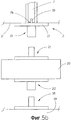
фиг.5а - схематичный вид спереди первой компоновки соединителя;figa is a schematic front view of the first layout of the connector;
фиг.5b - схематичный вид спереди второй компоновки соединителя;5b is a schematic front view of a second connector arrangement;
фиг.6 - схематичный вид в перспективе одномерной антенной решетки с линиями питания в соответствии с изобретением;6 is a schematic perspective view of a one-dimensional antenna array with power lines in accordance with the invention;
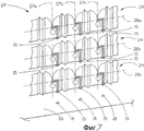
фиг.7 - схематичный вид в перспективе двумерной антенной решетки с линиями питания в соответствии с изобретением;7 is a schematic perspective view of a two-dimensional antenna array with power lines in accordance with the invention;
фиг.8а - схематичный вид в перспективе антенного элемента с двойной поляризацией, имеющего линии питания в соответствии с изобретением;Fig. 8a is a schematic perspective view of a dual polarized antenna element having power lines in accordance with the invention;
фиг.8b - схематичный вид сверху антенного элемента с двойной поляризацией, имеющего линии питания в соответствии с изобретением;Fig. 8b is a schematic top view of a dual polarized antenna element having power lines in accordance with the invention;
фиг.9 - схематичный вид сверху одномерной антенной решетки с двойной поляризацией, имеющей линии питания в соответствии с изобретением;Fig.9 is a schematic top view of a one-dimensional antenna array with double polarization having power lines in accordance with the invention;
фиг.10 - схематичный вид сверху двумерной антенной решетки с двойной поляризацией, имеющей линии питания в соответствии с изобретением;figure 10 is a schematic top view of a two-dimensional antenna array with double polarization having power lines in accordance with the invention;
фиг.11а - схематичный вид спереди первой одномерной щелевой антенной решетки;11 a is a schematic front view of a first one-dimensional slot antenna array;
фиг.11b - схематический вид спереди второй одномерной щелевой антенной решетки;11b is a schematic front view of a second one-dimensional slot antenna array;
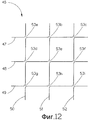
фиг.12 - относящийся ко второму варианту осуществления изобретения схематичный вид сверху второго варианта реализации двумерной антенной решетки с двойной поляризацией, соответствующей фиг.10;FIG. 12 is a schematic plan view of a second embodiment of the second embodiment of a two-dimensional dual polarization antenna array corresponding to FIG. 10;
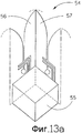
фиг.13а - схематичный вид в перспективе двумерной антенной решетки с двойной поляризацией, соединенной с питающим модулем;figa is a schematic perspective view of a two-dimensional antenna array with double polarization connected to the supply module;
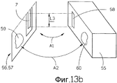
Фиг.13b - версия вида по фиг.13а с разнесенными элементами;Fig.13b is a version of the view of Fig.13a with exploded elements;
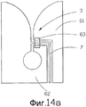
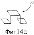
фиг.14а - схематичный вид спереди первого варианта реализации антенного элемента с линией питания в соответствии с изобретением, где линия питания оснащена металлической перемычкой;figa is a schematic front view of a first embodiment of an antenna element with a power line in accordance with the invention, where the power line is equipped with a metal jumper;
фиг.14b - первый вариант металлической перемычки;Fig.14b is a first variant of a metal jumper;
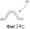
фиг.14с - второй вариант металлической перемычки;figs is a second variant of a metal jumper;
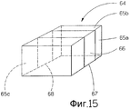
фиг.15 - металлическая перемычка, сформированная на диэлектрическом материале.Fig - metal jumper formed on a dielectric material.
Способы осуществления изобретенияMODES FOR CARRYING OUT THE INVENTION
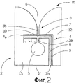
На фиг.1 показано схематичное представление антенного устройства в форме антенного элемента 1а с клиновидной щелью, например, типа «Vivaldi». Антенна 1а с клиновидной щелью содержит металлический слой 2 с щелевой линией 3, имеющей первую часть 3а и вторую часть 3b, причем щелевая линия 3 запитывается посредством линии 4 питания. Первая часть 3а щелевой линией 3 завершается, по существу, двумерной щелевой полостью 5. Вторая часть 3b щелевой линии 3 переходит в клиновидную щель 6 с открытым концом, образуя таким образом излучающий элемент. Антенный элемент 1а с клиновидной щелью выполнен только из одного единственного слоя 2 металла, образующего плоскость заземления, при этом линия 4 питания помещена в этот слой металла. Эта линия питания относится к типу копланарного волновода (CPW), который содержит питающую часть 7 в форме центрального проводника 7, отделенного от окружающей плоскости 2 заземления зазорами 8, 9. Линия 4 питания и ее центральный проводник 7 пересекает щелевую линию 3, разделяя ее на первую часть 3а и вторую часть 3b. Этот тип линии передачи является, по существу, линией передачи ТЕМ-типа (с поперечным электрическим и магнитным полем), аналогичной коаксиальной линии. Использование этой копланарной волноводной линии 4 питания делает возможным изготовление как линии 4 питания, так и клиновидной щели 6 в одном и том же слое 2 металла, который может быть листом металла, образующим металлический листовой слой 2.Figure 1 shows a schematic representation of an antenna device in the form of an antenna element 1A with a wedge-shaped slit, for example, such as "Vivaldi". The wedge-shaped antenna 1a comprises a
Центральный проводник 7 линии 4 питания имеет первый конец 7а и второй конец 7b, причем первый конец 7а пересекает щелевую линию 3. Второй конец 7b проходит к краю 2' металлического листового слоя 2. Первый конец 7а может заканчиваться многими способами: он может быть коротко замкнутым на конце, как показано для антенного элемента 1а на фиг.1, то есть непосредственно присоединяться к плоскости 2 заземления, сразу после прохождения им щелевой линии 3 с разделением ее на две части 3а, 3b.The
На фиг.2 показан антенный элемент 1b с клиновидной щелью, где центральный проводник 7 проходит щелевую линию 3 на длине L1, разделяя щелевую линию 3 на две части - 3а, 3b. Длина L1 прохода центрального проводника 7 приблизительно равна λg/2, то есть одной четверти длины волны в материале, так называемой длины волны в волноводе, где эта длина волны соответствует центральной частоте полосы частот антенны, и центральный проводник 7 короткозамкнут в своей конечной точке 7а, в результате чего короткозамкнутый центральный проводник 7 трансформируется как короткозамкнутый в точке 10 возбуждения щели.Figure 2 shows the
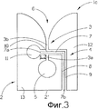
На фиг.3 показан антенный элемент 1с с клиновидной щелью, где центральный проводник 7 проходит щелевую линию 3, разделяя ее на две части: 3а, 3b. Длина L2 прохода центрального проводника 7 приблизительно равна λg/4, и центральный проводник 7 имеет открытый конец в своей конечной точке 7а, где он проходит в двумерную полость 11 на линии питания, аналогичной двумерной полости 5 на щели, которая завершает щелевую линию 3 на ее конце, наиболее удаленном от клиновидной щели 6. Следовательно, центральный проводник 7 с открытым концом трансформируется таким образом, чтобы быть короткозамкнутым в точке 10 возбуждения щели.Figure 3 shows the antenna element 1C with a wedge-shaped slit, where the
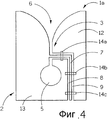
Изготовление такого антенного элемента 1а, 1b, 1с с клиновидной щелью может быть выполнено посредством перфорирования металлического листа. Поскольку в таком случае металлический лист будет разделен на две отдельные части 12, 13, то может быть необходимо механически поддерживать эту структуру в некоторых местах для того, чтобы сохранять общую структуру и функцию антенного элемента 1а, 1b, 1с, как это проиллюстрировано при помощи антенного элемента 1а на фиг.4, на которой показан вариант осуществления изобретения, соответствующий фиг.1. В варианте осуществления изобретения, соответствующем фиг.1, центральный проводник 7 будет составлять отдельную часть, которую будет необходимо поддерживать таким же образом по отношению к остальной структуре. Предпочтительно, чтобы поддержка, показанная на фиг.4, осуществлялась в «некритических» местах, то есть поддерживающие металлические или пластмассовые держатели 14а, 14b, 14с должны быть расположены там, где они никоим заметным образом не оказывают влияние на электрическое поле. Либо материал держателей 14а, 14b, 14с выбирается таким, что он имеет такие диэлектрические свойства, что он не оказывает влияние на электрические характеристики, либо, в ином случае, питающая линия 4 согласуется для адаптации к держателям 14а, 14b, 14с. Кроме того, держатели 14а, 14b, 14с также могут, например, образовывать перемычки (на чертеже не показаны) между двумя частями 12, 13, огибая центральный проводник 7, и могут в таком случае быть выполнены из металла.The manufacture of such an
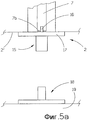
Центральный проводник 7, заканчивающийся на одном краю 2' металлического листа 2, как подробно показано на фиг.5а, может быть соединен с любой подходящей внешней схемой питания. Может быть использован некоторый вид соединителя 15, например SMA-соединитель (тип радиочастотного соединителя, монтируемый на винтах) или SMB-соединитель (тип радиочастотного соединителя, устанавливаемый на защелках). Внутренний проводник 16 соединителя 15 прикрепляется ко второму концу 7b центрального проводника 7 посредством, например, пайки, а внешний проводник 17 соединителя 15, то есть его заземление, прикрепляется к плоскости 2 заземления в виде металлического листа также посредством, например, пайки. Соответствующий соединитель 18 прикреплен к внешней схеме питания 19, например к распределяющей схеме питания.The
На фиг.5b между антенной и внешней схемой питания установлен посредством промежуточных соединителей 21, 22 питающий модуль 20, предназначенный для приема и/или передачи, например так называемый T/R-модуль (модуль передачи/приема), причем питающий модуль 20 может быть, например, активного типа, то есть содержать усилительные блоки, или пассивного типа. Питающий модуль 20 может также содержать регулируемые фазовращатели и аттенюаторы мощности. Питающий модуль 20 может быть соединен с блоком управления (на чертеже не показан) для управления мощностью и фазой. Используемую копланарную волноводную линию питания также удобно напрямую интегрировать с питающим модулем 20, отказавшись при этом от первой пары соединителей 17, 21, показанных на фиг.5b. Питающие модули 20 могут быть также частью внешней схемы питания 19, которая, в таком случае, сама составляет питающий модуль.In Fig. 5b, between the antenna and the external power circuit, a
Посредством перфорирования множества антенных элементов из более длинного листа металла 23 может быть изготовлена одномерная антенная решетка 24, показанная на фиг.6, состоящая из нескольких антенных элементов 1а, описанных выше, при этом антенная решетка 24 может иметь центральные проводники 7 с соответствующими соединителями 15, прикрепленными к их краям так, как это было описано выше. Эти соединители 15 могут затем быть прикреплены к соответствующим соединителям 18, смонтированным на внешней схеме питания 19, например на схеме распределения. Также могут быть использованы промежуточные питающие модули 20, показанные на фиг.5b (не показаны на фиг.6), или модули, интегрированные во внешнюю схему питания 19 и предназначенные для питания антенных элементов 1а в антенной решетке 24 таким образом, чтобы ориентировать главный лепесток диаграммы направленности антенной решетки в различных направлениях вдоль антенной решетки. Для того чтобы сделать антенную решетку более жесткой, этот лист может быть согнут, образуя малые соответствующие зубцы 25а, 25b, 25с, 25d, как это показано на фиг.6.By punching a plurality of antenna elements from a longer sheet of
Антенная решетка 24, показанная на фиг.6, оснащена антенными элементами 1а с копланарной волноводной питающей линией в соответствии с вариантом осуществления изобретения, показанным на фиг.1. Конечно, здесь и в нижеследующих примерах антенной решетки, где показан вариант осуществления изобретения в соответствии с фиг.1 с антенным элементом 1а с клиновидной щелью, может быть использован любой из антенных элементов 1а, 1b, 1с с их соответствующими вариантами реализации копланарной волноводной питающей линии, описанными выше со ссылкой на фиг.1-3. В этом и нижеследующих примерах вариантов реализации антенны могут повсюду, где это необходимо, применяться держатели 14а, 14b, 14с, описанные со ссылкой на фиг.4.The
Помещая множество антенных решеток 24, соответствующих вышеописанной, рядом друг с другом, можно получить двумерную антенную решетку 24', состоящую из рядов 26а, 26b, 26с и столбцов 27а, 27b, 27с, что показано на фиг.7. Ряды 26а, 26b, 26с могут иметь различное смещение относительно друг друга, в зависимости от требуемых свойств излучения. Как описано выше, это множество антенных решеток 24 соединено с внешней схемой питания 19 посредством соответствующих соединителей 15, 18, причем внешняя схема питания 19 может представлять собой схему распределения. Также могут быть использованы промежуточные питающие модули 20, показанные на фиг.5b (не показаны на фиг.7), или модули, интегрированные во внешнюю схему питания 19 и предназначенные для питания антенных элементов 1а в рядах 26а, 26b, 26с и столбцах 27а, 27b, 27с двумерной антенной решетки таким образом, чтобы ориентировать главный лепесток диаграммы направленности антенной решетки в различных направлениях вдоль рядов 26а, 26b, 26с и столбцов 27а, 27b, 27с антенной решетки.By placing a plurality of
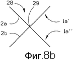
На фиг.8а и 8b показана антенна 28 с двойной поляризацией. Антенный элемент 28 с двойной поляризацией содержит два расположенных ортогонально антенных элемента 1а', 1а''. Металлические листы 2а, 2b, которые образуют антенну 28 с двойной поляризацией, размещены здесь таким образом, что они пересекают друг друга. Чтобы сделать возможным такое размещение, в металлических листах должны быть сделаны соответствующие монтажные прорези (на чертеже не показаны). Эти монтажные прорези описаны ниже. Следует, однако, отметить, что питающие линии 4а, 4b должны быть разнесены вертикально для исключения ситуации, когда центральные проводники 4а, 4b соприкасались бы друг с другом при пересечении. Предпочтительно, чтобы в точке 29 пересечения, показанной на виде сверху на фиг.8b, предусматривалась пайка, чтобы обеспечить хорошее электрическое соединение между металлическими листами 2а, 2b. Антенна 28 с двойной поляризацией излучает главные лепестки, которые ортогональны по отношению друг к другу, и ее питание также может осуществляться для излучения волн с круговой поляризацией.On figa and 8b shows the
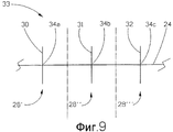
Посредством добавления ортогональных антенных элементов 30, 31, 32 к одномерной антенной решетке 24, показанной на фиг.6, получается одномерная антенная решетка 33 с двойной поляризацией, показанная на виде сверху на фиг.9. Таким образом, антенные элементы расположены в ортогональных парах 28', 28'', 28''', соответствующих антенному элементу с двойной поляризацией, показанному на фиг.8а и фиг.8b, излучающих в ортогональных направлениях. Для того чтобы сделать возможным такое размещение, в металлических листах должны быть сделаны соответствующие монтажные прорези (на чертеже не показаны). Антенны 30, 31, 32 размещены таким образом, что они пересекают друг друга. Предпочтительно в точках 34а, 34b, 34с пересечения предусмотрена пайка, чтобы обеспечить хорошее электрическое соединение.By adding the
Зубцы (25а-d), показанные на фиг.6 и 7, не показаны на фиг.9-13. Благодаря более жесткой структуре, обусловленной ортогонально размещенными антенными элементами, в вышеприведенном примере и в нижеследующих примерах также зубцы можно не выполнять.The teeth (25a-d) shown in FIGS. 6 and 7 are not shown in FIGS. 9-13. Due to the more rigid structure due to orthogonally placed antenna elements, in the above example and in the following examples, the teeth can also not be performed.
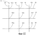
Посредством ортогонального добавления одномерных антенных решеток 24, соответствующих антенной решетке, показанной на фиг.6, к двумерной антенной решетке 25, показанной на фиг.7, получается двумерная антенная решетка 35 с двойной поляризацией, показанная на виде сверху на фиг.10, то есть антенные элементы расположены в ортогональных парах по двум измерениям, излучая в ортогональных направлениях. Металлические листы 36, 37, 38, 39, 40, 41 размещены здесь таким образом, что они пересекают друг друга, и их точки 42а, 42b, 42c, 42d, 42e, 42f, 42g, 42h, 42i пересечения могут находиться либо между каждым антенным элементом, либо в середине каждого антенного элемента. Для того чтобы сделать возможным такое размещение, в металлических листах должны быть сделаны соответствующие монтажные прорези (на чертеже не показаны). Предпочтительно, чтобы в точках 42а, 42b, 42c, 42d, 42e, 42f, 42g, 42h, 42i пересечения предусматривалась пайка, чтобы обеспечить хорошее электрическое соединение.By orthogonally adding the one-
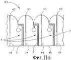
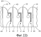
Одномерная антенная решетка 24, снабженная монтажными прорезями 43, 44, описанная выше, показана в двух различных вариантах осуществления изобретения на фиг.11а и фиг.11b. Монтажные прорези 43 одного ряда антенной решетки показаны сплошной линией, а монтажные прорези 44 соответствующего ему ряда антенной решетки показаны пунктирной линией. Ряды антенной решетки с монтажными прорезями 44, показанными пунктирной линией, размещаются ортогонально на рядах антенной решетки с монтажными прорезями 43, показанными сплошной линией, что позволяет прорезям 43, 44 закрепляться друг в друге. Прорези 43, 44 могут быть также выполнены в середине каждой клиновидной щелевой линии 3 (не показано), но в таком случае питающие линии 4 должны будут быть разнесены по вертикали, чтобы избежать их соприкосновения при пересечении, как описано выше со ссылкой на фиг.8а и 8b.A one-
На фиг.11а центральные проводники 7 копланарных волноводных линий 4 питания проходят к краю 45 металлического листа. На фиг.11b центральный проводник 7 копланарной волноводной линии 4 питания заканчивается до достижения им края 45 металлического листа. Вторая из этих двух конфигураций дополнительно описана ниже. Следует, однако, отметить, что вариант осуществления изобретения, соответствующий фиг.11b, не приводит в результате к отдельным металлическим частям, которые должны удерживаться относительно друг друга соответствующим способом, и обеспечивает взаимосвязанную структуру.11 a, the
На фиг.12 показана другая двумерная антенная решетка 46 с двойной поляризацией. Перфорированные металлические листы 47, 48, 49, 50, 51, 52 упорядочены в зигзагообразной структуре таким образом, что получается конструкция, аналогичная варианту осуществления изобретения, соответствующему показанному на фиг.10. Точки 53а, 53b, 53c, 53d, 53e, 53f, 53g, 53h, 53i пересечения располагаются здесь между сгибами в зигзагообразной структуре, причем эти сгибы и точки 53а, 53b, 53c, 53d, 53e, 53f, 53g, 53h, 53i пересечения могут быть расположены либо между каждым антенным элементом, либо в середине каждого антенного элемента. Предпочтительно, чтобы в точках 53а, 53b, 53c, 53d, 53e, 53f, 53g, 53h, 53i пересечения предусматривалась пайка, чтобы обеспечить хорошее электрическое соединение.On Fig shows another two-
Все эти антенные элементы в вариантах реализации с двойной поляризацией, описанных выше, как и в предыдущих случаях с одной поляризацией, соединены с внешней схемой питания 19, 20 посредством соответствующих соединений, причем внешняя схема питания 19, 20 может представлять собой схему распределения, которая может содержать средство, предназначенное для приема и/или передачи, например так называемый T/R-модуль (модуль передачи/приема), активного или пассивного типа. Схема питания 19, 20 может также содержать регулируемые фазовращатели и аттенюаторы мощности. Схема питания 19, 20 может быть соединена с блоком управления (на чертежах не показан) для управления мощностью и фазой. Таким образом, питание антенных элементов 1а, 1а', 1a'', 1b, 1c, 30, 31, 32 в столбцах и рядах антенной решетки 24, 24', 33, 35, 46 может осуществляться таким образом, чтобы ориентировать главный лепесток диаграммы направленности антенной решетки в различных направлениях вдоль столбцов и рядов антенной решетки для каждой из двух поляризаций. Питание антенных элементов в вариантах реализации с двойной поляризацией, описанных выше, может также осуществляться таким образом, что обеспечивается круговая поляризация.All of these antenna elements in the dual polarization embodiments described above, as in the previous cases with single polarization, are connected to an external
Фиг.13а и фиг.13b раскрывают возможный вариант питания антенной решетки 54 с двойной поляризацией, соответствующей фиг.10 или фиг.12, имеющей центральные проводники 7, соответствующие фиг.11b, не проходящие до конца вниз до края 45 металлического листа. На фиг.13b эта структура показана с разнесением элементов, как указано стрелками А1 и А2. Вставной питающий модуль 55, по существу, кубический или имеющий форму прямоугольного параллелепипеда, пригнанный к промежутку, образованному окружающими элементами 56, 57 антенны 54, размещен в каждом таком промежутке, образованном решетчатой структурой антенной решетки 54. Вставной питающий модуль 55 приспособлен для приема и/или передачи и может быть, например, активного или пассивного типа. Вставной питающий модуль 55 может также содержать питающую схему, регулируемые фазовращатели и аттенюаторы мощности. Вставной питающий модуль 55 может быть соединен с блоком управления для управления мощностью и фазой (на чертежах не показаны). Вставной питающий модуль 55 имеет, по меньшей мере, один соединяющий проводник 58 для присоединения центрального проводника 7 антенного элемента 56, 57, причем соединяющий проводник 58 имеет длину L3, которая, по существу, равна λg/4, что обеспечивает надежное соединение. Длина λg/4 соединяющего проводника 58 приводит в результате к тому, что не требуется, чтобы между соединяющим проводником 58 и соответствующим центральным проводником 7 имелся идеальный гальванический контакт. Центральный проводник 7 антенного элемента на фиг.11b показан незамкнутым, но может быть короткозамкнутым, если он скомпенсирован по возникающей связи.Figa and Fig.13b reveal a possible power supply of the antenna array with
Если вставной питающий модуль 55 рассеивает тепло, например, когда активные компоненты нагреваются при их использовании, то антенная структура 54 может быть использована в качестве охлаждающего фланца для вставных питающих модулей 55. В таком случае могут быть выбраны соответствующие области 59, 60 для передачи тепла от вставных модулей к антенной структуре. Эти области предпочтительно покрываются теплопроводным материалом известного вида.If the plug-in
При использовании в антенне 54 с двойной поляризацией, показанной на фиг.13а, каждый вставной питающий модуль 55 имеет два соединяющих проводника (не показаны на чертеже), питающих два антенных элемента 56, 57 с различными поляризациями. Этот вид питания антенных элементов 56, 57 при помощи соединяющих проводников 58, соединенных с центральным проводником 7, может быть также применен для других вариантов осуществления изобретения. Вставные питающие модули 55, используемые в антенной решетке 54, могут быть выполнены для питания антенных элементов 56, 57 таким образом, чтобы получить круговую поляризацию.When used in the
Понятно, что плоскость, на которую опираются вставные питающие модули, не является плоскостью заземления. Эта плоскость может быть снабжена соответствующими соединителями, которые соединяют каждый вставной питающий модуль 55 с его схемой питания, например, содержащей радиочастотные сигналы, сигналы электропитания и управляющие сигналы (на чертеже не показано).It is understood that the plane on which the plug-in supply modules rest is not a ground plane. This plane may be provided with appropriate connectors that connect each plug-in
Изобретение не должно быть ограничено рассмотренными выше вариантами осуществления, но может изменяться в пределах объема прилагаемой формулы изобретения. Например, зубцы 24а, 24b, 24с, 24d металлических листов антенной решетки могут быть выполнены и спрофилированы многими способами; показанная конструкция зубца является лишь одним из многих примеров.The invention should not be limited to the embodiments discussed above, but may vary within the scope of the appended claims. For example, the
Кроме того, конфигурация антенной решетки, соответствующая фиг.6, может быть выполнена без держателей 14а, 14b, 14с, показанных на фиг.4, поскольку отдельные металлические части 21а, 21b, 21c, 21d, составляющие антенную решетку 21, могут быть индивидуально прикреплены к внешней схеме питания 19 соответствующим образом, например, посредством приклеивания. Дополнительная устойчивость обеспечивается посредством соединителей 15, 18.In addition, the antenna array configuration corresponding to FIG. 6 can be made without the
Антенные решетки 24, 24', 33, 35, 46, 54, описанные выше, могут дополнительно поддерживаться посредством помещения между металлическим листом или металлическими листами, образующими антенную решетку, соответствующего поддерживающего материала, предпочтительно пеноматериала, такого как полиуретановый пенопласт, поскольку он должен быть экономичным, не вызывать потерь и не искажать диаграмму направленности антенны.The
Выше рассмотрены различные питающие модули 19, 20, 55. В пределах объема данного изобретения можно представить себе другие способы соединения активных или пассивных питающих модулей с антенными элементами.Various
Форма щели антенных элементов может изменяться, клиновидная щель 6 может иметь различные формы например она может расширяться ступенчато. Первая часть 3а щели может заканчиваться многими способами например упомянутой двумерной полостью 5, или коротко замыкаться на металлический листовой слой 2 на подходящем расстоянии от точки 10 возбуждения.The shape of the slit of the antenna elements may vary, the wedge-shaped
Антенные элементы могут изготавливаться множеством способов. Выше упомянуто перфорирование. Другими примерами являются лазерная резка, травление, механическая обработка и резка водяной струей. Если изготавливаемая антенна будет состоять из множества отдельных частей, то эти части могут быть сначала соединены маленькими соединительными планками, позволяющими легко ею манипулировать. Когда антенна правильно и надежно смонтирована, эти маленькие планки могут быть удалены.Antenna elements can be manufactured in a variety of ways. Perforation mentioned above. Other examples are laser cutting, pickling, machining and water jet cutting. If the antenna being manufactured will consist of many separate parts, then these parts can first be connected by small connecting strips, making it easy to manipulate. When the antenna is correctly and securely mounted, these small trims can be removed.
В другом не проиллюстрированном варианте осуществления изобретения антенная структура может быть вытравлена на элементе подложки, например подложки на основе политетрафторэтилена. Металл полностью удаляется с одной стороны подложки, и затем металл на другой стороне образует антенный элемент. Также используется другой аналогичный элемент подложки без металла с обеих сторон, при этом антенный элемент зажимается между этими двумя подложками. Элемент подложки без металла используется для обеспечения симметрии. Поскольку имеется только один слой металла, то не будет создаваться никаких мод параллельных пластин.In another, not illustrated embodiment, the antenna structure may be etched on a substrate element, for example a polytetrafluoroethylene-based substrate. The metal is completely removed on one side of the substrate, and then the metal on the other side forms an antenna element. Another similar substrate element without metal on both sides is also used, while the antenna element is clamped between the two substrates. A metal-free substrate element is used to provide symmetry. Since there is only one layer of metal, no parallel plate modes will be created.
Во всех вариантах осуществления, показанных выше, волновое сопротивление копланарной волноводной питающей линии 4 будет определяться шириной центрального проводника 7, шириной щелевой линии 3 и толщиной металлического листа 2. Предпочтительно, чтобы щелевая линия была, по существу, прямой, но она может также быть слегка клиновидной.In all the embodiments shown above, the impedance of the coplanar
Как показано на фиг.14а, плоскость 2 заземления содержит две отдельные плоскости 61, 62 заземления, окружающие центральный проводник 7 копланарного волновода 4. Как известно в данной области техники, предпочтительно, чтобы эти окружающие плоскости 61, 62 заземления были электрически соединены около точки возбуждения, то есть там, где центральный проводник 7 пересекает щелевую линию 3. Это достигается, например, посредством, по меньшей мере, одной металлической перемычки 63, которая получается сгибанием тонкого прямоугольного куска металла или металлического провода. Металлическая перемычка 63 припаивается (или приклеивается электропроводящим клеем) к окружающим плоскостям 61, 62 заземления непосредственно перед щелью 3, соединяя плоскости 61, 62 заземления, не контактируя с центральным проводником 7.As shown in FIG. 14 a, the
Металлическая перемычка 63 может быть согнута в форме с острыми углами, как показано на фиг.14b, где перемычка 63 получена сгибанием прямоугольного куска металла. Металлическая перемычка 63 может также быть согнута более плавно, по форме более или менее полукруга 63', как показано на фиг.14с, где перемычка 63 получена сгибанием металлической проволоки. Конечно, можно использовать либо только одну металлическую перемычку на одной из сторон, либо одну металлическую перемычку на каждой стороне. Последнее является предпочтительным, поскольку в таком случае электрическое соединение обеспечивается в более высокой степени и не нарушается симметрия.The
Согласно фиг.15 альтернативный вариант, по отношению к выполнению металлической перемычки, заключается в использовании элемента из диэлектрического материала 64, предпочтительно имеющего форму коробки с, по существу, перпендикулярными сторонами. Вдоль трех расположенных друг за другом сторон 65а, 65b, 65с диэлектрического материала 64 проходит проводник 66 из медной фольги в «U»-образной форме, у которого два края 67, 68 вводятся в электрический контакт с окружающими плоскостями 61, 62 заземления, показанными на фиг.14а, посредством, например, припаивания или приклеивания электропроводным клеем. Проводник 66 может быть выполнен посредством, например, травления, прокатывания или трафаретной печати.According to Fig. 15, an alternative with respect to the construction of the metal bridge is to use an element of
Металлические перемычки 63, 63', 64, описанные выше, являются лишь примерами того, как может быть выполнена металлическая перемычка, важным признаком является то, что плоскости 61, 62 заземления, окружающие центральный проводник 7 копланарного волновода 4, вводятся в электрический контакт друг с другом вблизи от точки возбуждения, то есть щели. Используемые металлическая перемычка или перемычки должны, однако, создавать как можно меньше помех копланарной волноводной структуре.The
Металлические перемычки 63, 63', 64, соответствующие вышеописанному, предпочтительно должны использоваться для всех вариантов осуществления изобретения, причем для тех вариантов осуществления изобретения, где центральный проводник копланарного волновода проходит щель и продолжается далее (например, в вариантах осуществления изобретения, соответствующих фиг.2 и 3), металлические перемычки должны быть использованы как до, так и после щели, и тогда в предпочтительном случае в результате имеется в общей сложности четыре металлические перемычки, по две на каждой стороне.The metal bridges 63, 63 ′, 64 corresponding to the above should preferably be used for all embodiments of the invention, and for those embodiments of the invention where the center conductor of the coplanar waveguide extends through the slot and continues further (for example, in the embodiments of the invention corresponding to FIG. 2 and 3) the metal jumpers must be used both before and after the gap, and then in the preferred case, as a result, there are a total of four metal jumpers and, two on each side.
Антенна с клиновидной щелью, описанная в вариантах осуществления изобретения, может относиться к типу щелевого элемента «Vivaldi». Возможны и другие типы антенных элементов, которые могут быть выполнены в соответствии с данным изобретением, в единственном металлическом слое и запитываться от питающей линии, например, симметричная вибраторная антенна ранее известного типа.The wedge-shaped antenna described in embodiments of the invention may be of the Vivaldi slot type. There are other types of antenna elements that can be made in accordance with this invention, in a single metal layer and fed from a supply line, for example, a symmetric vibrating antenna of a previously known type.
Claims (23)
Applications Claiming Priority (3)
| Application Number | Priority Date | Filing Date | Title |
|---|---|---|---|
| PCT/SE2003/002102 WO2005064747A1 (en) | 2003-12-30 | 2003-12-30 | Antenna device, and array antenna, with planar notch element feed |
| SEPCT/SE2003/002102 | 2003-12-30 | ||
| SE?CT/SE2003/002102 | 2003-12-30 |
Publications (2)
| Publication Number | Publication Date |
|---|---|
| RU2006123262A RU2006123262A (en) | 2008-01-10 |
| RU2359373C2 true RU2359373C2 (en) | 2009-06-20 |
Family
ID=34738118
Family Applications (1)
| Application Number | Title | Priority Date | Filing Date |
|---|---|---|---|
| RU2006123262/09A RU2359373C2 (en) | 2003-12-30 | 2004-12-27 | Feed line of planar edge element |
Country Status (5)
| Country | Link |
|---|---|
| US (1) | US7403169B2 (en) |
| EP (1) | EP1700359B1 (en) |
| AU (1) | AU2003294197A1 (en) |
| RU (1) | RU2359373C2 (en) |
| WO (2) | WO2005064747A1 (en) |
Cited By (1)
| Publication number | Priority date | Publication date | Assignee | Title |
|---|---|---|---|---|
| RU2729962C1 (en) * | 2019-02-22 | 2020-08-13 | Бейдзин Сяоми Мобайл Софтвэр Ко., Лтд. | Antenna unit and electronic device |
Families Citing this family (154)
| Publication number | Priority date | Publication date | Assignee | Title |
|---|---|---|---|---|
| CA2503793A1 (en) | 2002-10-22 | 2004-05-06 | Jason A. Sullivan | Systems and methods for providing a dynamically modular processing unit |
| EP1557075A4 (en) | 2002-10-22 | 2010-01-13 | Sullivan Jason | Non-peripherals processing control module having improved heat dissipating properties |
| CA2504222C (en) | 2002-10-22 | 2012-05-22 | Jason A. Sullivan | Robust customizable computer processing system |
| US7113142B2 (en) * | 2004-10-21 | 2006-09-26 | The Boeing Company | Design and fabrication methodology for a phased array antenna with integrated feed structure-conformal load-bearing concept |
| EP1684382A1 (en) * | 2005-01-19 | 2006-07-26 | Samsung Electronics Co., Ltd. | Small ultra wideband antenna having unidirectional radiation pattern |
| US20070164842A1 (en) * | 2006-01-19 | 2007-07-19 | Lumera Corporation | Electro-Optic Radiometer to Detect Radiation |
| US7486247B2 (en) * | 2006-02-13 | 2009-02-03 | Optimer Photonics, Inc. | Millimeter and sub-millimeter wave detection |
| US7679575B1 (en) * | 2006-06-15 | 2010-03-16 | The United States Of America As Represented By The Secretary Of The Navy | Tapered slot antenna cylindrical array |
| US7652631B2 (en) * | 2007-04-16 | 2010-01-26 | Raytheon Company | Ultra-wideband antenna array with additional low-frequency resonance |
| TWI334241B (en) * | 2007-05-10 | 2010-12-01 | Asustek Comp Inc | Antenna |
| EP2191538B1 (en) | 2007-08-22 | 2017-12-20 | BAE Systems PLC | Deployable lens antenna |
| US20090237315A1 (en) * | 2008-03-20 | 2009-09-24 | Shi-Lin Huang | Multi-input, multi-output antenna device |
| CN101609921A (en) * | 2008-06-20 | 2009-12-23 | 鸿富锦精密工业(深圳)有限公司 | Mobile communication device |
| JP5246115B2 (en) * | 2008-09-30 | 2013-07-24 | 日立電線株式会社 | ANTENNA AND ELECTRONIC DEVICE HAVING ANTENNA |
| FR2939243A1 (en) * | 2008-11-28 | 2010-06-04 | Thales Sa | Active antenna element, has ventilator configured and arranged in manner to force circulation of exterior air, where exterior air is inputted through one of faces of element and outputted through other face of element |
| CN102013575B (en) * | 2009-09-08 | 2015-07-22 | 日立金属株式会社 | Antenna and electronic device equipped with same |
| WO2012109393A1 (en) | 2011-02-08 | 2012-08-16 | Henry Cooper | High gain frequency step horn antenna |
| WO2012109498A1 (en) | 2011-02-09 | 2012-08-16 | Henry Cooper | Corrugated horn antenna with enhanced frequency range |
| WO2013124897A1 (en) * | 2012-02-23 | 2013-08-29 | 日本電気株式会社 | Antenna apparatus |
| US9685707B2 (en) * | 2012-05-30 | 2017-06-20 | Raytheon Company | Active electronically scanned array antenna |
| US9257747B2 (en) * | 2012-06-30 | 2016-02-09 | Taoglas Group Holdings Limited | Vivaldi-monopole antenna |
| US9270027B2 (en) * | 2013-02-04 | 2016-02-23 | Sensor And Antenna Systems, Lansdale, Inc. | Notch-antenna array and method for making same |
| US9450309B2 (en) * | 2013-05-30 | 2016-09-20 | Xi3 | Lobe antenna |
| US9999038B2 (en) | 2013-05-31 | 2018-06-12 | At&T Intellectual Property I, L.P. | Remote distributed antenna system |
| US9525524B2 (en) | 2013-05-31 | 2016-12-20 | At&T Intellectual Property I, L.P. | Remote distributed antenna system |
| US8897697B1 (en) | 2013-11-06 | 2014-11-25 | At&T Intellectual Property I, Lp | Millimeter-wave surface-wave communications |
| CN104810613B (en) * | 2014-01-26 | 2018-06-26 | 华为终端(东莞)有限公司 | A kind of terminal antenna configuration and terminal |
| US9768833B2 (en) | 2014-09-15 | 2017-09-19 | At&T Intellectual Property I, L.P. | Method and apparatus for sensing a condition in a transmission medium of electromagnetic waves |
| US10063280B2 (en) | 2014-09-17 | 2018-08-28 | At&T Intellectual Property I, L.P. | Monitoring and mitigating conditions in a communication network |
| US9615269B2 (en) | 2014-10-02 | 2017-04-04 | At&T Intellectual Property I, L.P. | Method and apparatus that provides fault tolerance in a communication network |
| US9685992B2 (en) | 2014-10-03 | 2017-06-20 | At&T Intellectual Property I, L.P. | Circuit panel network and methods thereof |
| US9503189B2 (en) | 2014-10-10 | 2016-11-22 | At&T Intellectual Property I, L.P. | Method and apparatus for arranging communication sessions in a communication system |
| US9973299B2 (en) | 2014-10-14 | 2018-05-15 | At&T Intellectual Property I, L.P. | Method and apparatus for adjusting a mode of communication in a communication network |
| US9577306B2 (en) | 2014-10-21 | 2017-02-21 | At&T Intellectual Property I, L.P. | Guided-wave transmission device and methods for use therewith |
| US9769020B2 (en) | 2014-10-21 | 2017-09-19 | At&T Intellectual Property I, L.P. | Method and apparatus for responding to events affecting communications in a communication network |
| US9312919B1 (en) | 2014-10-21 | 2016-04-12 | At&T Intellectual Property I, Lp | Transmission device with impairment compensation and methods for use therewith |
| US9780834B2 (en) | 2014-10-21 | 2017-10-03 | At&T Intellectual Property I, L.P. | Method and apparatus for transmitting electromagnetic waves |
| US9653770B2 (en) | 2014-10-21 | 2017-05-16 | At&T Intellectual Property I, L.P. | Guided wave coupler, coupling module and methods for use therewith |
| US9627768B2 (en) | 2014-10-21 | 2017-04-18 | At&T Intellectual Property I, L.P. | Guided-wave transmission device with non-fundamental mode propagation and methods for use therewith |
| US10009067B2 (en) | 2014-12-04 | 2018-06-26 | At&T Intellectual Property I, L.P. | Method and apparatus for configuring a communication interface |
| US10340573B2 (en) | 2016-10-26 | 2019-07-02 | At&T Intellectual Property I, L.P. | Launcher with cylindrical coupling device and methods for use therewith |
| US9544006B2 (en) | 2014-11-20 | 2017-01-10 | At&T Intellectual Property I, L.P. | Transmission device with mode division multiplexing and methods for use therewith |
| US9800327B2 (en) | 2014-11-20 | 2017-10-24 | At&T Intellectual Property I, L.P. | Apparatus for controlling operations of a communication device and methods thereof |
| US9742462B2 (en) | 2014-12-04 | 2017-08-22 | At&T Intellectual Property I, L.P. | Transmission medium and communication interfaces and methods for use therewith |
| US10243784B2 (en) | 2014-11-20 | 2019-03-26 | At&T Intellectual Property I, L.P. | System for generating topology information and methods thereof |
| US9954287B2 (en) | 2014-11-20 | 2018-04-24 | At&T Intellectual Property I, L.P. | Apparatus for converting wireless signals and electromagnetic waves and methods thereof |
| US9461706B1 (en) | 2015-07-31 | 2016-10-04 | At&T Intellectual Property I, Lp | Method and apparatus for exchanging communication signals |
| US9997819B2 (en) | 2015-06-09 | 2018-06-12 | At&T Intellectual Property I, L.P. | Transmission medium and method for facilitating propagation of electromagnetic waves via a core |
| US9876570B2 (en) | 2015-02-20 | 2018-01-23 | At&T Intellectual Property I, Lp | Guided-wave transmission device with non-fundamental mode propagation and methods for use therewith |
| US10389008B2 (en) | 2015-02-26 | 2019-08-20 | Ramot At Tel-Aviv University Ltd. | Technique for improving efficiency of on-chip antennas |
| US9749013B2 (en) | 2015-03-17 | 2017-08-29 | At&T Intellectual Property I, L.P. | Method and apparatus for reducing attenuation of electromagnetic waves guided by a transmission medium |
| US10224981B2 (en) | 2015-04-24 | 2019-03-05 | At&T Intellectual Property I, Lp | Passive electrical coupling device and methods for use therewith |
| US9705561B2 (en) | 2015-04-24 | 2017-07-11 | At&T Intellectual Property I, L.P. | Directional coupling device and methods for use therewith |
| US9793954B2 (en) | 2015-04-28 | 2017-10-17 | At&T Intellectual Property I, L.P. | Magnetic coupling device and methods for use therewith |
| US9871282B2 (en) | 2015-05-14 | 2018-01-16 | At&T Intellectual Property I, L.P. | At least one transmission medium having a dielectric surface that is covered at least in part by a second dielectric |
| US9490869B1 (en) | 2015-05-14 | 2016-11-08 | At&T Intellectual Property I, L.P. | Transmission medium having multiple cores and methods for use therewith |
| US9748626B2 (en) | 2015-05-14 | 2017-08-29 | At&T Intellectual Property I, L.P. | Plurality of cables having different cross-sectional shapes which are bundled together to form a transmission medium |
| US10650940B2 (en) | 2015-05-15 | 2020-05-12 | At&T Intellectual Property I, L.P. | Transmission medium having a conductive material and methods for use therewith |
| US9917341B2 (en) | 2015-05-27 | 2018-03-13 | At&T Intellectual Property I, L.P. | Apparatus and method for launching electromagnetic waves and for modifying radial dimensions of the propagating electromagnetic waves |
| US10812174B2 (en) | 2015-06-03 | 2020-10-20 | At&T Intellectual Property I, L.P. | Client node device and methods for use therewith |
| US9912381B2 (en) | 2015-06-03 | 2018-03-06 | At&T Intellectual Property I, Lp | Network termination and methods for use therewith |
| US9866309B2 (en) | 2015-06-03 | 2018-01-09 | At&T Intellectual Property I, Lp | Host node device and methods for use therewith |
| US9913139B2 (en) | 2015-06-09 | 2018-03-06 | At&T Intellectual Property I, L.P. | Signal fingerprinting for authentication of communicating devices |
| US9820146B2 (en) | 2015-06-12 | 2017-11-14 | At&T Intellectual Property I, L.P. | Method and apparatus for authentication and identity management of communicating devices |
| US9991605B2 (en) | 2015-06-16 | 2018-06-05 | The Mitre Corporation | Frequency-scaled ultra-wide spectrum element |
| US10056699B2 (en) | 2015-06-16 | 2018-08-21 | The Mitre Cooperation | Substrate-loaded frequency-scaled ultra-wide spectrum element |
| US9640850B2 (en) | 2015-06-25 | 2017-05-02 | At&T Intellectual Property I, L.P. | Methods and apparatus for inducing a non-fundamental wave mode on a transmission medium |
| US9865911B2 (en) | 2015-06-25 | 2018-01-09 | At&T Intellectual Property I, L.P. | Waveguide system for slot radiating first electromagnetic waves that are combined into a non-fundamental wave mode second electromagnetic wave on a transmission medium |
| US9509415B1 (en) | 2015-06-25 | 2016-11-29 | At&T Intellectual Property I, L.P. | Methods and apparatus for inducing a fundamental wave mode on a transmission medium |
| US9628116B2 (en) | 2015-07-14 | 2017-04-18 | At&T Intellectual Property I, L.P. | Apparatus and methods for transmitting wireless signals |
| US9882257B2 (en) | 2015-07-14 | 2018-01-30 | At&T Intellectual Property I, L.P. | Method and apparatus for launching a wave mode that mitigates interference |
| US10044409B2 (en) | 2015-07-14 | 2018-08-07 | At&T Intellectual Property I, L.P. | Transmission medium and methods for use therewith |
| US9847566B2 (en) | 2015-07-14 | 2017-12-19 | At&T Intellectual Property I, L.P. | Method and apparatus for adjusting a field of a signal to mitigate interference |
| US10205655B2 (en) | 2015-07-14 | 2019-02-12 | At&T Intellectual Property I, L.P. | Apparatus and methods for communicating utilizing an antenna array and multiple communication paths |
| US10148016B2 (en) | 2015-07-14 | 2018-12-04 | At&T Intellectual Property I, L.P. | Apparatus and methods for communicating utilizing an antenna array |
| US9853342B2 (en) | 2015-07-14 | 2017-12-26 | At&T Intellectual Property I, L.P. | Dielectric transmission medium connector and methods for use therewith |
| US10090606B2 (en) | 2015-07-15 | 2018-10-02 | At&T Intellectual Property I, L.P. | Antenna system with dielectric array and methods for use therewith |
| US9948333B2 (en) | 2015-07-23 | 2018-04-17 | At&T Intellectual Property I, L.P. | Method and apparatus for wireless communications to mitigate interference |
| US9871283B2 (en) | 2015-07-23 | 2018-01-16 | At&T Intellectual Property I, Lp | Transmission medium having a dielectric core comprised of plural members connected by a ball and socket configuration |
| US9749053B2 (en) | 2015-07-23 | 2017-08-29 | At&T Intellectual Property I, L.P. | Node device, repeater and methods for use therewith |
| US9912027B2 (en) | 2015-07-23 | 2018-03-06 | At&T Intellectual Property I, L.P. | Method and apparatus for exchanging communication signals |
| US9967173B2 (en) | 2015-07-31 | 2018-05-08 | At&T Intellectual Property I, L.P. | Method and apparatus for authentication and identity management of communicating devices |
| US9735833B2 (en) | 2015-07-31 | 2017-08-15 | At&T Intellectual Property I, L.P. | Method and apparatus for communications management in a neighborhood network |
| US9904535B2 (en) | 2015-09-14 | 2018-02-27 | At&T Intellectual Property I, L.P. | Method and apparatus for distributing software |
| US9769128B2 (en) | 2015-09-28 | 2017-09-19 | At&T Intellectual Property I, L.P. | Method and apparatus for encryption of communications over a network |
| US9729197B2 (en) | 2015-10-01 | 2017-08-08 | At&T Intellectual Property I, L.P. | Method and apparatus for communicating network management traffic over a network |
| US9876264B2 (en) | 2015-10-02 | 2018-01-23 | At&T Intellectual Property I, Lp | Communication system, guided wave switch and methods for use therewith |
| US10355367B2 (en) | 2015-10-16 | 2019-07-16 | At&T Intellectual Property I, L.P. | Antenna structure for exchanging wireless signals |
| EP3199957B1 (en) * | 2016-01-29 | 2020-12-30 | Rohde & Schwarz GmbH & Co. KG | Over the air measurement module |
| US10230172B1 (en) * | 2016-02-19 | 2019-03-12 | Rockwell Collins, Inc. | Thin metal ultra-wideband antenna array systems and methods |
| CN105826667A (en) * | 2016-03-15 | 2016-08-03 | 南京信息工程大学 | Novel small Vivaldi antenna |
| US9860075B1 (en) | 2016-08-26 | 2018-01-02 | At&T Intellectual Property I, L.P. | Method and communication node for broadband distribution |
| US10374316B2 (en) | 2016-10-21 | 2019-08-06 | At&T Intellectual Property I, L.P. | System and dielectric antenna with non-uniform dielectric |
| US10811767B2 (en) | 2016-10-21 | 2020-10-20 | At&T Intellectual Property I, L.P. | System and dielectric antenna with convex dielectric radome |
| US10312567B2 (en) | 2016-10-26 | 2019-06-04 | At&T Intellectual Property I, L.P. | Launcher with planar strip antenna and methods for use therewith |
| US10498044B2 (en) | 2016-11-03 | 2019-12-03 | At&T Intellectual Property I, L.P. | Apparatus for configuring a surface of an antenna |
| US10224634B2 (en) | 2016-11-03 | 2019-03-05 | At&T Intellectual Property I, L.P. | Methods and apparatus for adjusting an operational characteristic of an antenna |
| US10225025B2 (en) | 2016-11-03 | 2019-03-05 | At&T Intellectual Property I, L.P. | Method and apparatus for detecting a fault in a communication system |
| US10291334B2 (en) | 2016-11-03 | 2019-05-14 | At&T Intellectual Property I, L.P. | System for detecting a fault in a communication system |
| US10178445B2 (en) | 2016-11-23 | 2019-01-08 | At&T Intellectual Property I, L.P. | Methods, devices, and systems for load balancing between a plurality of waveguides |
| US10090594B2 (en) | 2016-11-23 | 2018-10-02 | At&T Intellectual Property I, L.P. | Antenna system having structural configurations for assembly |
| US10340603B2 (en) | 2016-11-23 | 2019-07-02 | At&T Intellectual Property I, L.P. | Antenna system having shielded structural configurations for assembly |
| US10340601B2 (en) | 2016-11-23 | 2019-07-02 | At&T Intellectual Property I, L.P. | Multi-antenna system and methods for use therewith |
| US10535928B2 (en) | 2016-11-23 | 2020-01-14 | At&T Intellectual Property I, L.P. | Antenna system and methods for use therewith |
| US10361489B2 (en) | 2016-12-01 | 2019-07-23 | At&T Intellectual Property I, L.P. | Dielectric dish antenna system and methods for use therewith |
| US10305190B2 (en) | 2016-12-01 | 2019-05-28 | At&T Intellectual Property I, L.P. | Reflecting dielectric antenna system and methods for use therewith |
| US9927517B1 (en) | 2016-12-06 | 2018-03-27 | At&T Intellectual Property I, L.P. | Apparatus and methods for sensing rainfall |
| US10755542B2 (en) | 2016-12-06 | 2020-08-25 | At&T Intellectual Property I, L.P. | Method and apparatus for surveillance via guided wave communication |
| US10727599B2 (en) | 2016-12-06 | 2020-07-28 | At&T Intellectual Property I, L.P. | Launcher with slot antenna and methods for use therewith |
| US10020844B2 (en) | 2016-12-06 | 2018-07-10 | T&T Intellectual Property I, L.P. | Method and apparatus for broadcast communication via guided waves |
| US10637149B2 (en) | 2016-12-06 | 2020-04-28 | At&T Intellectual Property I, L.P. | Injection molded dielectric antenna and methods for use therewith |
| US10819035B2 (en) | 2016-12-06 | 2020-10-27 | At&T Intellectual Property I, L.P. | Launcher with helical antenna and methods for use therewith |
| US10135145B2 (en) | 2016-12-06 | 2018-11-20 | At&T Intellectual Property I, L.P. | Apparatus and methods for generating an electromagnetic wave along a transmission medium |
| US10694379B2 (en) | 2016-12-06 | 2020-06-23 | At&T Intellectual Property I, L.P. | Waveguide system with device-based authentication and methods for use therewith |
| US10382976B2 (en) | 2016-12-06 | 2019-08-13 | At&T Intellectual Property I, L.P. | Method and apparatus for managing wireless communications based on communication paths and network device positions |
| US10439675B2 (en) | 2016-12-06 | 2019-10-08 | At&T Intellectual Property I, L.P. | Method and apparatus for repeating guided wave communication signals |
| US10326494B2 (en) | 2016-12-06 | 2019-06-18 | At&T Intellectual Property I, L.P. | Apparatus for measurement de-embedding and methods for use therewith |
| US10359749B2 (en) | 2016-12-07 | 2019-07-23 | At&T Intellectual Property I, L.P. | Method and apparatus for utilities management via guided wave communication |
| US10547348B2 (en) | 2016-12-07 | 2020-01-28 | At&T Intellectual Property I, L.P. | Method and apparatus for switching transmission mediums in a communication system |
| US10027397B2 (en) | 2016-12-07 | 2018-07-17 | At&T Intellectual Property I, L.P. | Distributed antenna system and methods for use therewith |
| US9893795B1 (en) | 2016-12-07 | 2018-02-13 | At&T Intellectual Property I, Lp | Method and repeater for broadband distribution |
| US10168695B2 (en) | 2016-12-07 | 2019-01-01 | At&T Intellectual Property I, L.P. | Method and apparatus for controlling an unmanned aircraft |
| US10446936B2 (en) | 2016-12-07 | 2019-10-15 | At&T Intellectual Property I, L.P. | Multi-feed dielectric antenna system and methods for use therewith |
| US10389029B2 (en) | 2016-12-07 | 2019-08-20 | At&T Intellectual Property I, L.P. | Multi-feed dielectric antenna system with core selection and methods for use therewith |
| US10243270B2 (en) | 2016-12-07 | 2019-03-26 | At&T Intellectual Property I, L.P. | Beam adaptive multi-feed dielectric antenna system and methods for use therewith |
| US10139820B2 (en) | 2016-12-07 | 2018-11-27 | At&T Intellectual Property I, L.P. | Method and apparatus for deploying equipment of a communication system |
| US10530505B2 (en) | 2016-12-08 | 2020-01-07 | At&T Intellectual Property I, L.P. | Apparatus and methods for launching electromagnetic waves along a transmission medium |
| US10326689B2 (en) | 2016-12-08 | 2019-06-18 | At&T Intellectual Property I, L.P. | Method and system for providing alternative communication paths |
| US10777873B2 (en) | 2016-12-08 | 2020-09-15 | At&T Intellectual Property I, L.P. | Method and apparatus for mounting network devices |
| US10916969B2 (en) | 2016-12-08 | 2021-02-09 | At&T Intellectual Property I, L.P. | Method and apparatus for providing power using an inductive coupling |
| US9911020B1 (en) | 2016-12-08 | 2018-03-06 | At&T Intellectual Property I, L.P. | Method and apparatus for tracking via a radio frequency identification device |
| US10069535B2 (en) | 2016-12-08 | 2018-09-04 | At&T Intellectual Property I, L.P. | Apparatus and methods for launching electromagnetic waves having a certain electric field structure |
| US9998870B1 (en) | 2016-12-08 | 2018-06-12 | At&T Intellectual Property I, L.P. | Method and apparatus for proximity sensing |
| US10938108B2 (en) | 2016-12-08 | 2021-03-02 | At&T Intellectual Property I, L.P. | Frequency selective multi-feed dielectric antenna system and methods for use therewith |
| US10411356B2 (en) | 2016-12-08 | 2019-09-10 | At&T Intellectual Property I, L.P. | Apparatus and methods for selectively targeting communication devices with an antenna array |
| US10601494B2 (en) | 2016-12-08 | 2020-03-24 | At&T Intellectual Property I, L.P. | Dual-band communication device and method for use therewith |
| US10103422B2 (en) | 2016-12-08 | 2018-10-16 | At&T Intellectual Property I, L.P. | Method and apparatus for mounting network devices |
| US10389037B2 (en) | 2016-12-08 | 2019-08-20 | At&T Intellectual Property I, L.P. | Apparatus and methods for selecting sections of an antenna array and use therewith |
| US10340983B2 (en) | 2016-12-09 | 2019-07-02 | At&T Intellectual Property I, L.P. | Method and apparatus for surveying remote sites via guided wave communications |
| US10264586B2 (en) | 2016-12-09 | 2019-04-16 | At&T Mobility Ii Llc | Cloud-based packet controller and methods for use therewith |
| US9838896B1 (en) | 2016-12-09 | 2017-12-05 | At&T Intellectual Property I, L.P. | Method and apparatus for assessing network coverage |
| CN106532270B (en) * | 2016-12-29 | 2019-08-27 | 南京信息职业技术学院 | Resistance loaded miniaturized Vivaldi antenna for electromagnetic radiation measurement system |
| US9973940B1 (en) | 2017-02-27 | 2018-05-15 | At&T Intellectual Property I, L.P. | Apparatus and methods for dynamic impedance matching of a guided wave launcher |
| US10298293B2 (en) | 2017-03-13 | 2019-05-21 | At&T Intellectual Property I, L.P. | Apparatus of communication utilizing wireless network devices |
| US10854993B2 (en) | 2017-09-18 | 2020-12-01 | The Mitre Corporation | Low-profile, wideband electronically scanned array for geo-location, communications, and radar |
| US10468737B2 (en) * | 2017-12-30 | 2019-11-05 | Intel Corporation | Assembly and manufacturing friendly waveguide launchers |
| US10886625B2 (en) | 2018-08-28 | 2021-01-05 | The Mitre Corporation | Low-profile wideband antenna array configured to utilize efficient manufacturing processes |
| CN110174649B (en) * | 2019-05-07 | 2024-07-19 | 加特兰微电子科技(上海)有限公司 | RF front-end transceiver, vehicle-mounted radar transceiver system |
| CN111490342B (en) * | 2020-04-24 | 2021-06-01 | 电子科技大学 | Ultra-wideband dual-polarized lens antenna based on Vivaldi antenna form |
| CN113054415B (en) * | 2021-04-01 | 2022-09-13 | 北京有竹居网络技术有限公司 | Antennas and Terminals |
| CN113381183B (en) * | 2021-06-10 | 2022-01-25 | 华南理工大学 | Anti-sufficient Vivaldi antenna based on artificial surface plasmon polariton |
| CN115528426B (en) * | 2021-06-25 | 2025-04-08 | 中国移动通信集团终端有限公司 | Antenna array and router |
| CN114744419B (en) * | 2022-03-14 | 2023-05-02 | 中国电子科技集团公司第二十九研究所 | Orthogonal polarization wide bandwidth angle scanning phased array antenna |
| CN115360497B (en) * | 2022-07-22 | 2024-04-05 | 青岛大学 | A flexible wearable ultra-wideband CPW antenna and preparation method thereof |
Citations (3)
| Publication number | Priority date | Publication date | Assignee | Title |
|---|---|---|---|---|
| EP0455493A2 (en) * | 1990-05-04 | 1991-11-06 | Motorola, Inc. | Tapered notch antenna |
| US5142255A (en) * | 1990-05-07 | 1992-08-25 | The Texas A&M University System | Planar active endfire radiating elements and coplanar waveguide filters with wide electronic tuning bandwidth |
| FR2691014A1 (en) * | 1985-10-11 | 1993-11-12 | Thomson Csf | Waveguide antenna for radar ECM - has two logarithmic shaped launchers with opposite phase feed mounted in waveguide |
Family Cites Families (8)
| Publication number | Priority date | Publication date | Assignee | Title |
|---|---|---|---|---|
| US4853704A (en) * | 1988-05-23 | 1989-08-01 | Ball Corporation | Notch antenna with microstrip feed |
| US5519408A (en) * | 1991-01-22 | 1996-05-21 | Us Air Force | Tapered notch antenna using coplanar waveguide |
| US5748153A (en) * | 1994-11-08 | 1998-05-05 | Northrop Grumman Corporation | Flared conductor-backed coplanar waveguide traveling wave antenna |
| JP3550859B2 (en) * | 1996-03-05 | 2004-08-04 | 三菱電機株式会社 | Tapered slot antenna |
| US6239761B1 (en) * | 1996-08-29 | 2001-05-29 | Trw Inc. | Extended dielectric material tapered slot antenna |
| US6043785A (en) * | 1998-11-30 | 2000-03-28 | Radio Frequency Systems, Inc. | Broadband fixed-radius slot antenna arrangement |
| US6292153B1 (en) * | 1999-08-27 | 2001-09-18 | Fantasma Network, Inc. | Antenna comprising two wideband notch regions on one coplanar substrate |
| US6963312B2 (en) * | 2001-09-04 | 2005-11-08 | Raytheon Company | Slot for decade band tapered slot antenna, and method of making and configuring same |
-
2003
- 2003-12-30 WO PCT/SE2003/002102 patent/WO2005064747A1/en not_active Ceased
- 2003-12-30 AU AU2003294197A patent/AU2003294197A1/en not_active Abandoned
-
2004
- 2004-12-27 EP EP04809184.7A patent/EP1700359B1/en not_active Expired - Lifetime
- 2004-12-27 WO PCT/SE2004/002011 patent/WO2005064748A1/en not_active Ceased
- 2004-12-27 US US10/584,907 patent/US7403169B2/en not_active Expired - Fee Related
- 2004-12-27 RU RU2006123262/09A patent/RU2359373C2/en not_active IP Right Cessation
Patent Citations (3)
| Publication number | Priority date | Publication date | Assignee | Title |
|---|---|---|---|---|
| FR2691014A1 (en) * | 1985-10-11 | 1993-11-12 | Thomson Csf | Waveguide antenna for radar ECM - has two logarithmic shaped launchers with opposite phase feed mounted in waveguide |
| EP0455493A2 (en) * | 1990-05-04 | 1991-11-06 | Motorola, Inc. | Tapered notch antenna |
| US5142255A (en) * | 1990-05-07 | 1992-08-25 | The Texas A&M University System | Planar active endfire radiating elements and coplanar waveguide filters with wide electronic tuning bandwidth |
Cited By (1)
| Publication number | Priority date | Publication date | Assignee | Title |
|---|---|---|---|---|
| RU2729962C1 (en) * | 2019-02-22 | 2020-08-13 | Бейдзин Сяоми Мобайл Софтвэр Ко., Лтд. | Antenna unit and electronic device |
Also Published As
| Publication number | Publication date |
|---|---|
| US20070126648A1 (en) | 2007-06-07 |
| WO2005064748A1 (en) | 2005-07-14 |
| WO2005064747A1 (en) | 2005-07-14 |
| EP1700359A1 (en) | 2006-09-13 |
| AU2003294197A1 (en) | 2005-07-21 |
| EP1700359B1 (en) | 2014-04-02 |
| US7403169B2 (en) | 2008-07-22 |
| RU2006123262A (en) | 2008-01-10 |
Similar Documents
| Publication | Publication Date | Title |
|---|---|---|
| RU2359373C2 (en) | Feed line of planar edge element | |
| JP5983760B2 (en) | Array antenna | |
| EP1182731B1 (en) | Dual-polarized radiating element with high isolation between polarization channels | |
| US8130162B2 (en) | Broadband multi-dipole antenna with frequency-independent radiation characteristics | |
| JP6730290B2 (en) | Antenna array using sandwiched radiating elements above ground plane and fed by stripline | |
| US7215284B2 (en) | Passive self-switching dual band array antenna | |
| CN109494460B (en) | Dual-polarization/circularly-polarized broadband high-density antenna array with high isolation | |
| CN114639950B (en) | Dual polarization antenna | |
| US20040061656A1 (en) | Low profile wideband antenna array | |
| CN102257675A (en) | Dual frequency antenna aperture | |
| JP2004120760A (en) | Dual polarization antenna | |
| US11682838B2 (en) | Multiband antenna structure | |
| US6650299B2 (en) | Antenna apparatus | |
| GB2346012A (en) | Dual polarisation antennas | |
| CN119495926A (en) | Circularly polarized antennas, array antennas and communication equipment | |
| JP2007166629A (en) | Single polarization slot antenna array with inter-element coupling and associated method | |
| JP5078732B2 (en) | Antenna device | |
| JP2007166630A (en) | Dual polarization antenna array with inter-element capacitive coupling plate and associated method | |
| JPS6369301A (en) | Shared planar antenna for polarized wave | |
| JP2005086658A (en) | Polarization common use antenna | |
| JP3185406B2 (en) | Planar antenna | |
| JP2002290144A (en) | Planar array antenna | |
| EP3028341A1 (en) | Stacked bowtie radiator with integrated balun | |
| CN117578065B (en) | Low-cost 5G M-MIMO base station antenna array | |
| JP3068149B2 (en) | Microstrip array antenna |
Legal Events
| Date | Code | Title | Description |
|---|---|---|---|
| PC41 | Official registration of the transfer of exclusive right |
Effective date: 20160818 |
|
| PC41 | Official registration of the transfer of exclusive right |
Effective date: 20161014 |
|
| MM4A | The patent is invalid due to non-payment of fees |
Effective date: 20181228 |