RU2355103C1 - Pseudorandom sequence generator - Google Patents
Pseudorandom sequence generator Download PDFInfo
- Publication number
- RU2355103C1 RU2355103C1 RU2007140610/09A RU2007140610A RU2355103C1 RU 2355103 C1 RU2355103 C1 RU 2355103C1 RU 2007140610/09 A RU2007140610/09 A RU 2007140610/09A RU 2007140610 A RU2007140610 A RU 2007140610A RU 2355103 C1 RU2355103 C1 RU 2355103C1
- Authority
- RU
- Russia
- Prior art keywords
- input
- output
- feedback
- adder
- trigger
- Prior art date
Links
- 238000009434 installation Methods 0.000 claims description 8
- 230000000903 blocking effect Effects 0.000 claims description 6
- 239000000126 substance Substances 0.000 abstract 1
- 238000010586 diagram Methods 0.000 description 6
- 230000015572 biosynthetic process Effects 0.000 description 5
- 238000000034 method Methods 0.000 description 4
- 239000003990 capacitor Substances 0.000 description 2
- 230000003213 activating effect Effects 0.000 description 1
- 230000005540 biological transmission Effects 0.000 description 1
- 239000011159 matrix material Substances 0.000 description 1
- 239000004065 semiconductor Substances 0.000 description 1
Images

Landscapes
- Detection And Prevention Of Errors In Transmission (AREA)
Abstract
Description
Изобретение относится к области радиотехники и может использоваться в качестве генератора опорных сигналов в передатчиках и приемниках широкополосных сигналов.The invention relates to the field of radio engineering and can be used as a generator of reference signals in transmitters and receivers of broadband signals.
Известны генераторы псевдослучайной последовательностиPseudo-random sequence generators are known
Системы связи с шумоподобными сигналами, Варакина Л.Е. - М.: Радио и связь, 1985 с.50 рис.3.14 (Генератор М-последовательности), содержащие триггеры, сумматор по модулю два, недостатком которых является фиксированная, ограниченная длина и структура формируемой псевдослучайной последовательности.Communication systems with noise-like signals, L. Varakina - M .: Radio and communication, 1985 p.50 Fig. 3.14 (M-sequence generator), containing triggers, an adder modulo two, the disadvantage of which is a fixed, limited length and structure of the generated pseudo-random sequence.
Генератор псевдослучайной последовательности по патенту (RU №2003136964 от 22.12.2003 года, МПК Н 03/00, G06F 7/58). Он содержит генератор N/2-разрядной двоичной псевдослучайной последовательности, реализованной на регистре сдвига с линейными обратными связями. Его недостатком является фиксированная, ограниченная длина и структура формируемой псевдослучайной последовательности.The pseudo-random sequence generator according to the patent (RU No. 2003136964 dated December 22, 2003, IPC H 03/00,
Наиболее близким по технической сущности к заявляемому объекту является генератор псевдослучайной последовательности (RU №2223539 от 31.05.2002 года, МПК Н03В 29/00, G06F 7/58), содержащий генератор тактовых импульсов, группу из m-триггеров, m-умножителей, сумматор по модулю два, оперативно запоминающий блок, формирователь адреса, двухвходовый сумматор по модулю два, делитель частоты. Данный генератор псевдослучайных последовательностей, содержащий генератор тактовых импульсов, выход которого соединен с первыми сигнальными входами с первого по m триггеров соответственно, выходы которых через m умножителей соединены с n входами сумматора по модулю два соответственно, выход которого соединен со вторым сигнальным входом первого триггера, отличающийся тем, что введены последовательно соединенные делитель частоты, двухвходовый сумматор по модулю два и формирователь адреса, выход которого шиной соединен со вторым входом оперативно-запоминающего блока, первый вход которого соединен с выходом сумматора по модулю два. Кроме того, выход генератора тактовых импульсов соединен с входом делителя частоты и со вторым входом двухвходового сумматора по модулю два, выход которого соединен с третьим входом оперативно-запоминающего блока.The closest in technical essence to the claimed object is a pseudo-random sequence generator (RU No. 2223539 dated 05/31/2002, IPC Н03В 29/00, G06F 7/58), containing a clock pulse generator, a group of m-flip-flops, m-multipliers, an adder modulo two, random-access memory, address former, two-input adder modulo two, frequency divider. This pseudo-random sequence generator containing a clock generator whose output is connected to the first signal inputs from the first to m triggers, respectively, the outputs of which through m multipliers are connected to the n inputs of the adder modulo two, respectively, the output of which is connected to the second signal input of the first trigger, different by the fact that a frequency divider, a two-input adder modulo two, and an address former, the output of which is connected via a bus to the second input, are introduced operational memory unit, the first input coupled to an output of the adder of modulo two. In addition, the output of the clock generator is connected to the input of the frequency divider and to the second input of the two-input adder modulo two, the output of which is connected to the third input of the RAM.
Однако устройство-прототип имеет ограниченную область применения, обусловленную тем, что он формирует псевдослучайную последовательность фиксированной, ограниченной длины и только с фиксированным набором структур, это объясняется тем, что количество используемых для формирования псевдослучайной последовательности триггеров и умножителей не может изменяться, кроме этого, ближайший аналог имеет относительно низкую надежность, так как при выходе из строя любого из элементов, предназначенных для формирования псевдослучайной последовательности, генератор не выполняет своего функционального назначения.However, the prototype device has a limited scope, due to the fact that it forms a pseudo-random sequence of a fixed, limited length and only with a fixed set of structures, this is because the number of triggers and multipliers used to form a pseudo-random sequence cannot change, in addition, the closest the analogue has a relatively low reliability, since in case of failure of any of the elements designed to form a pseudo-random sequence telnosti, the generator does not fulfill its functional purpose.
Целью изобретения является разработка генератора псевдослучайной последовательности, обеспечивающего возможность расширения области его применения благодаря формированию последовательности различной длины и структуры. Заявленный генератор расширяет арсенал средств данного назначения.The aim of the invention is to develop a pseudo-random sequence generator, which provides the possibility of expanding its field of application due to the formation of sequences of different lengths and structures. The claimed generator expands the arsenal of tools for this purpose.
Поставленная цель достигается тем, что в известном генераторе псевдослучайной последовательности, содержащем сумматор по модулю два и генератор тактовых импульсов, выход которого подключен к тактовым входам М≥3 триггеров, дополнительно введены блок установки начального состояния, элемент запуска, элемент «ИЛИ», М коммутирующих элементов, М объединителей, N=M-1 элементов управления сумматором, N блоков обратной связи и N-1 сумматоров по модулю два.This goal is achieved by the fact that in the known generator of a pseudo-random sequence containing an adder modulo two and a clock generator, the output of which is connected to the clock inputs M≥3 triggers, an initial state setting unit, a trigger element, an “OR” element, M commuting elements are additionally introduced elements, M combiners, N = M-1 adder controls, N feedback blocks and N-1 adders modulo two.
Новым также является то, что выход блока установки начального состояния подключен к входам установки в состояние ноль М-триггеров и к входу элемента запуска. Выход элемента запуска подключен к первому входу элемента «ИЛИ», второй вход которого подключен к выходу первого блока обратной связи. Выход р-го, где р=1,2,…(М-1), коммутирующего элемента подключен к первому входу р-го объединителя, второй вход которого подключен к выходу р-го триггера. Выход р-го объединителя подключен к первому входу (р+1)-го коммутирующего элемента, информационному входу (р-1)-го триггера и информационному входу р-го элемента управления сумматором. Управляющий выход р-го элемента управления сумматором подключен к блокирующему входу р-го блока обратной связи, информационный вход которого подключен к выходу р-го сумматора по модулю два. Первый и второй информационные входы каждого сумматора подключены соответственно к первому и второму информационному выходам р-го элемента управления сумматором. Вход обратной связи р-го элемента управления сумматором и передающий вход р-го блока обратной связи подключены к информационному выходу (р+1)-го блока обратной связи. Выход М-го объединителя подключен к входу обратной связи N-го элемента управления сумматором и передающему входу N-го блока обратной связи и является выходом генератора случайной последовательности. Выход элемента «ИЛИ» подключен к второму входу первого коммутирующего элемента и информационному входу первого триггера. Первый вход m-го, где m=1,2,…М, коммутирующего элемента подключен к входу установки в состояние единица и к управляющему входу m-го триггера и является m-м управляющим входом генератора случайной последовательности, причем блокирующий вход n-го, где n=l,2,…N, элемента управления сумматором подключен к входу установки в состояние единица (n+1)-го триггера. Разрешающий вход n-го элемента управления сумматором является n-м управляющим входом обратной связи генератора псевдослучайной последовательности.Also new is the fact that the output of the initial state installation unit is connected to the inputs of the installation in the state zero of M-triggers and to the input of the trigger element. The output of the trigger element is connected to the first input of the OR element, the second input of which is connected to the output of the first feedback block. The output of the rth, where p = 1,2, ... (M-1), the switching element is connected to the first input of the rth combiner, the second input of which is connected to the output of the rth trigger. The output of the r-th combiner is connected to the first input of the (p + 1) -th switching element, the information input of the (r-1) -th trigger and the information input of the r-th adder control. The control output of the rth adder control element is connected to the blocking input of the rth feedback block, the information input of which is connected to the output of the rth adder modulo two. The first and second information inputs of each adder are connected respectively to the first and second information outputs of the rth adder control element. The feedback input of the rth adder control element and the transmitting input of the rth feedback unit are connected to the information output of the (p + 1) th feedback unit. The output of the Mth combiner is connected to the feedback input of the Nth adder control element and the transmitting input of the Nth feedback unit and is the output of a random sequence generator. The output of the OR element is connected to the second input of the first switching element and the information input of the first trigger. The first input of the mth, where m = 1,2, ... M, of the switching element is connected to the installation input in the state one and to the control input of the mth trigger and is the mth control input of the random sequence generator, and the input of the nth is blocking , where n = l, 2, ... N, the adder control is connected to the unit input to the state of the unit of the (n + 1) th trigger. The enable input of the nth adder control is the nth feedback control input of the pseudo-random sequence generator.
Заявленное устройство поясняется чертежами, где:The claimed device is illustrated by drawings, where:
Фиг 1: Структурная схема генератора псевдослучайной последовательностиFig 1: Block diagram of a pseudo-random sequence generator
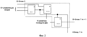
Фиг 2: Схема элемента управления сумматоромFig 2: Adder Control Diagram
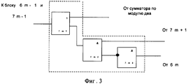
Фиг 3: Схема блока обратной связиFIG 3: Feedback block diagram
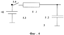
Фиг 4: Схема блока установки начального состоянияFig 4: Block diagram of the installation of the initial state
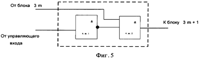
Фиг 5: Схема коммутирующего элементаFig 5: Diagram of a switching element
Фиг 6: Вариант схемы элемента запускаFig 6: Variant of a diagram of the trigger element
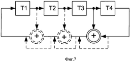
Фиг 7: Рисунок, поясняющий работу генератораFig 7: Figure illustrating the operation of the generator
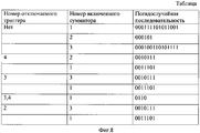
Фиг 8: Таблица структур псевдослучайных последовательностейFig 8: Table of structures of pseudo-random sequences
Генератор псевдослучайной последовательности, показанный на фиг.1, состоит из:The pseudo-random sequence generator shown in FIG. 1 consists of:
генератора тактовых импульсов (ГТИ) 1, М триггеров 21- 2М, М объединителей 31-3М, М-коммутирующих элементов (КЭ) 41-4М, блока установки начального состояния (БУНС) 5, N-элементов управления сумматором (ЭУС) 61-6N, N-блоков обратной связи (БОС) 71-7N, N-сумматоров по модулю 2 81-8N, элемента запуска (ЭЗ) 9, элемента «ИЛИ» 10 со связями между ними. Выход БУНС 5 подключен к входам установки в состояние ноль М триггеров 21-2М. Выход БУНС 5 подключен к входу ЭЗ 9. Выход ЭЗ 9 подключен к первому входу элемента «ИЛИ». Второй вход элемента «ИЛИ» подключен к выходу первого БОС. Выход р-го КЭ, где р=1,2,…(М-1), подключен к первому входу р-го объединителя 31-3М. Второй вход р-го объединителя 31-3М подключен к выходу р-го триггера 21-2М. Выход р-го объединителя 31-3М подключен к первому входу (р+1)-го КЭ 41-4М, информационному входу (р+1)-го триггера 21-2М и информационному входу р-го ЭУС 61-6N. Управляющий выход 61-6N подключен к блокирующему входу р-го БОС 71-7N. Информационный вход БОС 71-7N подключен к выходу р-го сумматора по модулю два 81-8N. Первый и второй информационные входы сумматора по модулю два 81-8N подключены соответственно к первому и второму информационному выходам р-го ЭУС 61-6N. Вход обратной связи р-го ЭУС 61-6N и передающий вход р-го БОС 71-7N подключены к информационному выходу (р+1)-го БОС 71-7N. Выход М-го объединителя 31-3М подключен к входу обратной связи N-го ЭУС 61-6N. Выход М-го объединителя 31-3М подключен к передающему входу N-го БОС 71-7N и является выходом генератора случайной последовательности. Выход элемента «ИЛИ» 10 подключен к второму входу первого КЭ 41-4М. Выход элемента «ИЛИ» 10 подключен к информационному входу первого триггера 21-2М. Первый вход m-го, где m=1,2,…М, КЭ 41 - 4 м, подключен к входу установки в состояние единица. Первый вход m-го, где m=1,2,…М, КЭ 41-4М, подключен к управляющему входу m-го триггера 21-2М и является m-м управляющим входом генератора случайной последовательности. Блокирующий вход n-го, где n=l,2,…N, ЭУС 61-6N подключен к входу установки в состояние единица (n+1)-го триггера 21-2М. Разрешающий вход n-го ЭУС 61-6N является n-м управляющим входом обратной связи генератора псевдослучайной последовательности.clock pulse generator (GTI) 1, M triggers 2 1 - 2 M , M combiners 3 1 -3 M , M-switching elements (CE) 4 1 -4 M , initial state setting unit (BUNS) 5, N-control elements by an adder (EUS) 6 1 -6 N , N-feedback units (BOS) 7 1 -7 N , N-
Входящие в общую структуру генератора псевдослучайной последовательности элементы могут быть реализованы в настоящее время при использовании имеющейся элементной базы:The elements included in the general structure of the pseudo-random sequence generator can be implemented at present using the available element base:
Генератор тактовых импульсов 1 может быть реализован путем применения интегральной схемы 2ГС191, как описано в книге: В.А.Батушев; Основы применения интегральных схем - ВАС, 1972. стр.83-84.The
Элементы "И", "ИЛИ", "ИЛИ-НЕ" известны и описаны, например, в книге: П.П.Мальцев, Н.С.Долидзе, М.И.Критенко и др. Цифровые интегральные микросхемы; Справочник. - М.: Радио и связь, 1994, стр.234-237.The elements "AND", "OR", "OR-NOT" are known and described, for example, in the book: P. P. Maltsev, N. S. Dolidze, M. I. Kritenko, etc. Digital Integrated Circuits; Directory. - M.: Radio and Communications, 1994, pp. 234-237.
DV-триггеры известны и описаны, например, в книге: В.А.Батушев, В.Н.Вениаминов, В.Г.Ковалев и др. Микросхемы и их применение: Справочное пособие. - М.: Энергия, 1978, стр.164-168.DV-triggers are known and described, for example, in the book: V. A. Batushev, V. N. Veniaminov, V. G. Kovalev and others. Microcircuits and their application: Reference manual. - M .: Energy, 1978, pp. 164-168.
Резистор 5.1 может быть реализован путем применения матрицы резисторов, описанных в книге: Б.В.Тарабрин, Л.Ф-Лунин, Ю.Н.Смирнов и др. Интегральные микросхемы; Справочник. - Издание второе, исправленное - М: Энергоатомиздат, 1985 г., стр.190.Resistor 5.1 can be implemented by using the matrix of resistors described in the book: B.V. Tarabrin, L.F-Lunin, Yu.N. Smirnov, etc. Integrated circuits; Directory. - Second edition, revised - M: Energoatomizdat, 1985, p. 190.
Конденсатор 5.2 может быть реализован путем применения конденсаторов, описанных в книге: P.M.Терещук, К.М.Терещук, С.А.Седов. Полупроводниковые приемно-усилительные устройства; Справочник радиолюбителя. - Издание второе, стереотипное. - Киев: Наукова думка, 1982 г., стр.44-62.Capacitor 5.2 can be implemented by using capacitors described in the book: P.M. Tereshchuk, K.M. Tereshchuk, S.A. Sedov. Semiconductor receiving and amplifying devices; Handbook of amateur radio. - Second edition, stereotyped. - Kiev: Naukova Dumka, 1982, pp. 44-62.
Сумматор по модулю два 81-8N известен и описан например, в книге: Ю.А.Беляев, А.В.Семенов; Теоретические основы вычислительной техники Часть 1-ЛВВИУС, 1988. - с.117-118.An adder modulo two 8 1 -8 N is known and described, for example, in the book: Yu.A. Belyaev, A.V. Semenov; Theoretical Foundations of Computer Engineering Part 1-LVVIUS, 1988. - pp. 117-118.
Схема элемента запуска 9, может быть реализована как переключатель механический, известный и описанный в книге: Ю.Л.Мазора, Е.А.Мачусского, В.И.Правды. Радиотехника: Энциклопедия. - М: Издательский дом «Додэка-XXI» 2002. стр.865The circuit of the trigger element 9, can be implemented as a mechanical switch, known and described in the book: Yu.L. Mazora, E.A. Machusky, V.I. Pravda. Radio Engineering: Encyclopedia. - M: Publishing house "Dodeca-XXI" 2002. p. 865
Генератор псевдослучайной последовательности работает следующим образом.The pseudo-random sequence generator operates as follows.
Подготовка устройства к работе заключается в установке всех элементов в исходное состояние:Preparing the device for work is to install all the elements in the initial state:
- триггеры 21,…,2M (Фиг.1) устанавливаются в состояние логического ноля, посредством кратковременной подачи на установочные входы R триггеров 21,…,2M высокого уровня сигнала от БУНС 5 (Фиг.4) при замыкании ключа 5.4 (Фиг.4) данного блока;- triggers 2 1 , ..., 2 M (Fig. 1) are set to a logical zero state by means of a short-term supply to the installation inputs R of
- на управляющие входы 1,…,М и управляющие входы обратной связи 1,…,N (Фиг.1) подаются сигналы, определяющие структуру псевдослучайной последовательности;- to the
- ГТИ 5 (Фиг.1) формирует сигналы тактовой синхронизации с частотой следования, соответствующей частоте формируемой псевдослучайной последовательности;- GTI 5 (Figure 1) generates clock synchronization signals with a repetition rate corresponding to the frequency of the generated pseudo-random sequence;
- элемент запуска 9 (Фиг.1,6) находится в отключенном состоянии.- the trigger element 9 (Fig.1.6) is in the off state.
Устройство-формирователь псевдослучайной последовательности работает в следующих режимах:The pseudo-random sequence driver device operates in the following modes:
формирование псевдослучайной последовательности максимальной длины и фиксированной структуры; формирование псевдослучайной последовательности переменной длины; формирование псевдослучайной последовательности разных структур.the formation of a pseudo-random sequence of maximum length and fixed structure; the formation of a pseudo-random sequence of variable length; the formation of a pseudo-random sequence of different structures.
При формировании псевдослучайной последовательности максимальной длины и фиксированной структуры, задействованы все триггеры 21,…,2M устройства. Сумматоры по модулю два 81-8N, ЭУС 61-6N, БОС 71-7N подключаются в соответствии с установленными правилами.When forming a pseudo-random sequence of maximum length and a fixed structure, all triggers of 2 1 , ..., 2 M devices are involved. The adders modulo two 8 1 -8 N , EUS 6 1 -6 N , BOS 7 1 -7 N are connected in accordance with the established rules.
Исходное состояние: на управляющие входы 1,…,М подается сигнал логической единицы, на управляющие входы обратной связи, за исключением одного, который определяет требуемую структуру формируемой псевдослучайной последовательности, подается сигнал логического ноля. Выбор входа обратной связи, определяющего структуру формируемой псевдослучайной последовательности, может проводиться по правилам, как показано, например, в книге: Варакин Л.Е. «Системы связи с шумоподобными сигналами - М.: Радио и связь, 1985, страница 59.Initial state: a logical unit signal is supplied to the
В данном случае устройство работает следующим образом: при замыкании контакта в элементе запуска 9 (Фиг.1, Фиг.6) сигнал логической единицы через элемент 10 ИЛИ (Фиг.1) подается на информационный вход триггера 21, с приходом синхронизирующего сигнала с генератора тактовых импульсов на синхронизирующие входы триггеров 21,…,2M данная единица записывается в триггер 21.In this case, the device operates as follows: when the contact is closed in the start element 9 (Fig. 1, Fig. 6), the signal of the logical unit through the element 10 OR (Fig. 1) is fed to the information input of the
При приходе следующего тактового импульса триггер 21 переходит в состояние логического нуля, триггер 22 переводится в состояние логической единицы. Таким образом, логическая единица последовательно по триггерам передвигается до триггера 2M.When the next clock pulse arrives,
При переводе триггера 2M в состояние логической единицы, к выходу которого подключен сумматор по модулю два, формирующий структуру псевдослучайной последовательности, начинает формироваться псевдослучайная последовательность. При этом структура псевдослучайной последовательности формируется посредством подачи сигналов по цепи обратной связи с выхода включенного сумматора по модулю два 81-8N, на вход элемента «ИЛИ» 10 (Фиг.1, Фиг.4) далее на информационный вход триггера 21. То же самое происходит при переходе М-го триггера в состояние логической единицы. Таким образом, формируется структура псевдослучайной последовательности.When the
При формировании псевдослучайной последовательности переменной длины часть триггеров исключается из процесса формирования псевдослучайной последовательности путем подачи на соответствующие 1,…,М (Фиг1.) управляющие входы сигнала логический ноль. В этом случае триггер будет находиться в отключенном состоянии, а на его выходе будет сигнал логического ноля. Сигнал логического ноля на управляющем входе отключает одноименный триггер, переводя его в состояние логического ноля, и обеспечивает прохождение информационного сигнала через коммутирующий элемент 4 (Фиг.5) на соответствующий объеденитель 3 (Фиг.1) подключенный к выключенному триггеру. Тот же сигнал логического ноля на управляющем входе через схему элемента управления сумматором по модулю два (Фиг.2) отключает сумматор по модулю два и обеспечивает прохождение по цепи обратной связи (Фиг.3) информационного сигнала формирующего структуру псевдослучайной последовательности. Прохождение информационного сигнала относительно задействованных (включенных в работу) триггеров осуществляется аналогично процессу формирования псевдослучайной последовательности максимальной длинны.When forming a pseudo-random sequence of variable length, part of the triggers is excluded from the process of forming a pseudo-random sequence by applying logical zero to the control inputs of the
Процесс передачи информации при отключении триггеров обеспечивается посредством работы схемы коммутирующего элемента. Если на управляющем входе будет сигнал логического ноля, элемент 4.m.1 (Фиг.5) подготовит элемент 4.m.2 к прохождению информационного сигнала, не задействуя одноименный отключенный триггер.The process of transmitting information when the triggers are turned off is provided through the operation of the switching element circuit. If there is a logic zero signal at the control input, element 4.m.1 (Figure 5) will prepare element 4.m.2 for the passage of the information signal without activating the trigger that has the same name.
Формирование псевдослучайной последовательности разных структур обеспечивается за счет отключения (включения) сумматоров по модулю два 8 (Фиг.1).The formation of a pseudo-random sequence of different structures is ensured by turning off (on) the adders modulo two 8 (Figure 1).
Во всех случаях соответствующий сумматор по модулю два включается одновременной подачей на одноименный управляющий вход обратной связи и соответствующий управляющий вход логической единицы. В этом случае сигнал на входах сумматора по модулю два будет определяться сигналами на выходах предыдущего и М-го объеденителей. Элементы 6.m.2 и 6.m.3 (Фиг.2) устройства управления сумматором по модулю два находятся в ожидающем режиме, так как на выходе элемента 6.m.1 будет сигнал логической единицы, который соответственно подается на один из входов элементов 6.m.2 и 6.m.3. В то же время элемент 7.m.2 (Фиг.3) блока обратной связи находится в состоянии запрещающем продвижение информационного сигнала, что исключает передачу сигнала обратной связи, минуя сумматор по модулю два.In all cases, the corresponding adder modulo two is turned on by simultaneously supplying the feedback control input of the same name and the corresponding control input of a logical unit. In this case, the signal at the inputs of the adder modulo two will be determined by the signals at the outputs of the previous and Mth combiners. Elements 6.m.2 and 6.m.3 (Figure 2) of the adder control module modulo two are in standby mode, since the output of element 6.m.1 will be a signal of a logical unit, which is respectively fed to one of the inputs elements 6.m.2 and 6.m.3. At the same time, the element 7.m.2 (Fig. 3) of the feedback block is in a state prohibiting the promotion of the information signal, which excludes the transmission of the feedback signal, bypassing the adder modulo two.
При наличии на управляющих входах схемы блока управления сумматором по модулю два (Фиг.1, Фиг.2) хотя бы одного логического ноля, что соответствует случаю отключения триггера из процесса формирования псевдослучайной последовательности (логический ноль на соответствующем управляющем входе (Фиг.1) или отключения сумматора по модулю два (логический ноль на управляющем входе обратной связи) в этом случае на выходах элементов 6.m.2 и 6.m.3 будет сигнал логического ноля, что обеспечит возможность передачи сигнала обратной связи, минуя сумматор по модулю два, так как элемент 7.m.1 и 7.m.2 (Фиг.3) в этом случае находятся в ожидающих режимах.If there are at least one logical zero on the control inputs of the adder control circuit modulo two (Fig. 1, Fig. 2), which corresponds to the case when the trigger is disconnected from the pseudo-random sequence generation process (logical zero on the corresponding control input (Fig. 1) or there are two modulo-off adders (logical zero at the feedback control input) in this case, the outputs of the elements 6.m.2 and 6.m.3 will have a logical zero signal, which will enable the feedback signal to be transmitted bypassing the adder via ulyu two since 7.m.1 element and 7.m.2 (3) in this case are in the waiting mode.
Таким образом, по сравнению с ближайшим аналогом заявленный генератор формирования псевдослучайной последовательности имеет большие функциональные возможности, поскольку может быть использован, например, для построения универсальных устройств тестирования каналов связи.Thus, in comparison with the closest analogue, the claimed pseudo-random sequence generator has great functionality, since it can be used, for example, to build universal devices for testing communication channels.
Claims (1)
Priority Applications (1)
| Application Number | Priority Date | Filing Date | Title |
|---|---|---|---|
| RU2007140610/09A RU2355103C1 (en) | 2007-11-01 | 2007-11-01 | Pseudorandom sequence generator |
Applications Claiming Priority (1)
| Application Number | Priority Date | Filing Date | Title |
|---|---|---|---|
| RU2007140610/09A RU2355103C1 (en) | 2007-11-01 | 2007-11-01 | Pseudorandom sequence generator |
Publications (1)
| Publication Number | Publication Date |
|---|---|
| RU2355103C1 true RU2355103C1 (en) | 2009-05-10 |
Family
ID=41020134
Family Applications (1)
| Application Number | Title | Priority Date | Filing Date |
|---|---|---|---|
| RU2007140610/09A RU2355103C1 (en) | 2007-11-01 | 2007-11-01 | Pseudorandom sequence generator |
Country Status (1)
| Country | Link |
|---|---|
| RU (1) | RU2355103C1 (en) |
Cited By (2)
| Publication number | Priority date | Publication date | Assignee | Title |
|---|---|---|---|---|
| RU2419224C1 (en) * | 2009-12-08 | 2011-05-20 | Открытое акционерное общество "Концерн "Созвездие" | Shaper of m-sequences |
| RU2634233C1 (en) * | 2017-01-12 | 2017-10-24 | Борис Иванович Крыжановский | Method of generating pseudo-random binary sequence |
Citations (4)
| Publication number | Priority date | Publication date | Assignee | Title |
|---|---|---|---|---|
| SU1750033A2 (en) * | 1990-06-11 | 1992-07-23 | Военный Инженерный Краснознаменный Институт Им.А.Ф.Можайского | Generator of pseudorandom sequences |
| SU1758851A2 (en) * | 1990-08-10 | 1992-08-30 | Ростовское высшее военное командно-инженерное училище ракетных войск | Generator of semi-random sequences |
| EP1164696A1 (en) * | 1999-12-24 | 2001-12-19 | Anritsu Corporation | Wonder generator, digital line tester comprising the same, and phase noise transfer characteristic analyzer |
| EP1330031A1 (en) * | 2002-01-21 | 2003-07-23 | Mitsubishi Electric Information Technology Centre Europe B.V. | Generation of a sequence of pulse trains |
-
2007
- 2007-11-01 RU RU2007140610/09A patent/RU2355103C1/en not_active IP Right Cessation
Patent Citations (4)
| Publication number | Priority date | Publication date | Assignee | Title |
|---|---|---|---|---|
| SU1750033A2 (en) * | 1990-06-11 | 1992-07-23 | Военный Инженерный Краснознаменный Институт Им.А.Ф.Можайского | Generator of pseudorandom sequences |
| SU1758851A2 (en) * | 1990-08-10 | 1992-08-30 | Ростовское высшее военное командно-инженерное училище ракетных войск | Generator of semi-random sequences |
| EP1164696A1 (en) * | 1999-12-24 | 2001-12-19 | Anritsu Corporation | Wonder generator, digital line tester comprising the same, and phase noise transfer characteristic analyzer |
| EP1330031A1 (en) * | 2002-01-21 | 2003-07-23 | Mitsubishi Electric Information Technology Centre Europe B.V. | Generation of a sequence of pulse trains |
Cited By (2)
| Publication number | Priority date | Publication date | Assignee | Title |
|---|---|---|---|---|
| RU2419224C1 (en) * | 2009-12-08 | 2011-05-20 | Открытое акционерное общество "Концерн "Созвездие" | Shaper of m-sequences |
| RU2634233C1 (en) * | 2017-01-12 | 2017-10-24 | Борис Иванович Крыжановский | Method of generating pseudo-random binary sequence |
Similar Documents
| Publication | Publication Date | Title |
|---|---|---|
| US9092067B2 (en) | Phase disciplined, direct digital synthesizer based, coherent signal generator | |
| US9047152B2 (en) | Delay device, method, and random number generator using the same | |
| EP0905611A2 (en) | Pseudorandom number generating method and pseudorandom number generator | |
| CN110231599A (en) | Radar equipment, radar system and the method for generating sampled clock signal | |
| RU2355103C1 (en) | Pseudorandom sequence generator | |
| JP2011250441A5 (en) | ||
| US6177891B1 (en) | Serial-parallel conversion apparatus | |
| KR970029796A (en) | Synchronous Semiconductor Circuit with Increased Driving Time Margin | |
| US7933310B2 (en) | System for a fast frequency hopping radio | |
| US7868679B2 (en) | Circuit, method for receiving a signal, and use of a random event generator | |
| JP2003304136A (en) | Infinite phase unit | |
| US7586348B2 (en) | Systems, apparatuses and methods for synchronizing clock signals | |
| RU92270U1 (en) | Pseudorandom Binary Sequence Generator | |
| Ying et al. | Design of BDS/GPS C/A Code Generator | |
| RU2427886C2 (en) | Generator of pseudorandom binary sequences | |
| WO2000039667A1 (en) | Code generator | |
| RU2618941C2 (en) | Correlator | |
| KR100617957B1 (en) | Reverse data sampling method and reverse data sampling circuit using same | |
| JPH03251890A (en) | Nonlinear feedback shift register device | |
| Al-Khalili et al. | A controlled probability random pulse generator suitable for VLSI implementation | |
| EP1215835B1 (en) | Synchronous acquisition device for cdma receiver | |
| RU2227370C2 (en) | Radio link ensuring enhanced hiding of information transferred | |
| RU2119245C1 (en) | Time relay | |
| RU2703283C1 (en) | Method for digital generation of phase-shift keyed radio signal with spread spectrum | |
| KR20100014070A (en) | Clock signal generator |
Legal Events
| Date | Code | Title | Description |
|---|---|---|---|
| MM4A | The patent is invalid due to non-payment of fees |
Effective date: 20091102 |