RU2180985C2 - Flip-flop unit - Google Patents
Flip-flop unit Download PDFInfo
- Publication number
- RU2180985C2 RU2180985C2 RU99116822A RU99116822A RU2180985C2 RU 2180985 C2 RU2180985 C2 RU 2180985C2 RU 99116822 A RU99116822 A RU 99116822A RU 99116822 A RU99116822 A RU 99116822A RU 2180985 C2 RU2180985 C2 RU 2180985C2
- Authority
- RU
- Russia
- Prior art keywords
- output
- trigger
- memory element
- resistor
- winding
- Prior art date
Links
Images

Abstract
Description
Изобретение относится к импульсной технике и может быть использовано в устройствах вычислительной техники и систем управления. The invention relates to a pulse technique and can be used in computing devices and control systems.
Известно триггерное устройство (см. авт. свид. СССР 845287 от 02.07.79, МКИ Н 03 К 19/16, опубл. 07.07.81, БИ 25. Н.М.Лукманов. Энергонезависимая ячейка памяти), содержащий сердечник с прямоугольной петлей гистерезиса и обмоткой, средняя точка которой подключена через резистор к источнику питания. Конец обмотки подключен к выходу первого элемента И-НЕ, начало - к выходу второго элемента И-НЕ и к одному из входов третьего элемента И-НЕ, второй вход которого подключен к шине разрешения, а выход - к единичному входу триггера. Нулевой вход триггера подключен к шине сброса, а прямой и инверсный выходы - к первым входам соответственно первого и второго элементов И-НЕ, вторые входы которых подключены к шине перемагничивания. Known trigger device (see ed. Certificate of the USSR 845287 from 02.07.79, MKI N 03 K 19/16, publ. 07.07.81, BI 25. N.M. Lukmanov. Non-volatile memory cell) containing a core with a rectangular loop hysteresis and winding, the middle point of which is connected through a resistor to a power source. The end of the winding is connected to the output of the first AND-NOT element, the beginning to the output of the second AND-NOT element and to one of the inputs of the third AND-NOT element, the second input of which is connected to the resolution bus, and the output is to the single input of the trigger. The trigger zero input is connected to the reset bus, and the direct and inverse outputs are connected to the first inputs of the first and second AND-NOT elements, respectively, the second inputs of which are connected to the magnetization reversal bus.
Недостатками данного триггерного устройства являются низкие помехоустойчивость и достоверность функционирования, так как вероятность сбоя триггера высока, а восстановление истинного состояния происходит лишь при очередном санкционированном опросе сердечника. Пока триггер находится в ложном состоянии, сигнал об этом не формируется, следовательно, внешними устройствами ложное состояние данного триггера воспринимается как истинное. The disadvantages of this trigger device are low noise immunity and reliability of operation, since the probability of a trigger failure is high, and the restoration of the true state occurs only at the next authorized interrogation of the core. While the trigger is in a false state, a signal about this is not formed, therefore, with external devices, the false state of this trigger is perceived as true.
Известно триггерное устройство (см. авт. свид. СССР 1019594 от 04.02.82, МКИ Н 03 К 3/286, опубл. 23.05.83, БИ 19. Г.И.Шишкин. Триггерное устройство (его варианты), (фиг.2)), содержащее триггер, логический элемент, первый и второй элементы памяти на магнитных сердечниках, выходы обмоток считывания которых соединены с общей шиной. Входы обмоток считывания подключены соответственно к катодам первого и второго диодов, аноды которых соединены с общей шиной через соответственно первый и второй конденсаторы и с шиной источника питания через соответственно первый и второй резисторы. Выходы обмоток записи первого и второго элементов памяти на магнитных сердечниках соединены между собой. Выход логического элемента подключены к тактовому входу триггера, прямой и инверсный выходы которого соединены соответственно с входами обмоток записи первого и второго элементов памяти на магнитных сердечниках. Первый и второй входы логического элемента соединены соответственно с анодами первого и второго диодов, причем его третий вход подключен к входной шине. A trigger device is known (see ed. Certificate of the USSR 1019594 dated 04.02.82, MKI N 03
Недостатком данного триггерного устройства является сложность, связанная с наличием двух элементов памяти на магнитных сердечниках и большого количества дискретных элементов (диодов, конденсаторов и резисторов), что затрудняет миниатюризацию устройства и уменьшает его надежность. The disadvantage of this trigger device is the complexity associated with the presence of two memory elements on the magnetic cores and a large number of discrete elements (diodes, capacitors and resistors), which complicates the miniaturization of the device and reduces its reliability.
Достигаемым техническим результатом является упрощение триггерного устройства путем уменьшения количества элементов памяти на магнитных сердечниках и других дискретных элементов. Achievable technical result is the simplification of the trigger device by reducing the number of memory elements on magnetic cores and other discrete elements.
Указанный технический результат достигается тем, что в триггерное устройство, содержащее триггер, логический элемент, элемент памяти на магнитном сердечнике, резистор и конденсатор, при этом инверсный выход триггера соединен с одним входом элемента памяти, а вывод резистора через конденсатор соединен с общей шиной, дополнительно введен триггер Шмитта, при этом другой вход элемента памяти соединен с прямым выходом триггера, а выходы - с соответствующими входами логического элемента, выход которого соединен с другим выводом резистора, вход триггера Шмитта подключен к точке соединения резистора и конденсатора, а выход соединен с тактовым входом триггера. The specified technical result is achieved by the fact that in a trigger device containing a trigger, a logic element, a memory element on a magnetic core, a resistor and a capacitor, the inverse output of the trigger is connected to one input of the memory element, and the output of the resistor through the capacitor is connected to a common bus, additionally Schmitt trigger is introduced, while the other input of the memory element is connected to the direct output of the trigger, and the outputs are connected to the corresponding inputs of the logic element, the output of which is connected to the other output of the resistor The Schmitt trigger is connected to the connection point of the resistor and capacitor, and the output is connected to the trigger clock input.
Кроме того, элемент памяти на магнитном сердечнике содержит магнитный сердечник с обмоткой и резистор, при этом один вывод обмотки является одним выходом элемента памяти и соединен с одним входом элемента памяти, другой вывод обмотки является другим выходом элемента памяти, а отвод обмотки через резистор соединен с другим входом элемента памяти, при этом логический элемент выполнен в виде элемента ИСКЛЮЧАЮЩЕЕ ИЛИ. In addition, the memory element on the magnetic core contains a magnetic core with a winding and a resistor, while one output of the winding is one output of the memory element and is connected to one input of the memory element, the other output of the winding is another output of the memory element, and the tap of the winding through the resistor is connected to another input of the memory element, while the logical element is made in the form of an exclusive OR element.
Кроме того, элемент памяти на магнитном сердечнике содержит магнитный сердечник с обмоткой, резистор и два инвертора с открытым стоком (коллектором), при этом один вывод обмотки является одним выходом элемента памяти и соединен с выходом первого инвертора, другой вывод - является другим выходом элемента памяти и соединен с выходом второго инвертора, а средняя точка обмотки через резистор подключена к шине питания, входы первого и второго инверторов являются одним и другим входами элемента памяти, а логический элемент выполнен в виде элемента ИЛИ. In addition, the memory element on the magnetic core contains a magnetic core with a winding, a resistor and two inverters with an open drain (collector), while one output of the winding is one output of the memory element and is connected to the output of the first inverter, the other output is another output of the memory element and connected to the output of the second inverter, and the middle point of the winding through the resistor is connected to the power bus, the inputs of the first and second inverters are one and the other inputs of the memory element, and the logic element is made in the form of an element nt OR.
Указанная совокупность признаков позволяет упростить триггерное устройство путем исключения второго элемента памяти на магнитном сердечнике, второго конденсатора и диодов. The specified set of features allows to simplify the trigger device by eliminating the second memory element on the magnetic core, the second capacitor and diodes.
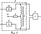
На фиг. 1 приведена схема триггерного устройства, а на фиг.2 и 3 - возможные варианты выполнения элемента памяти и логического элемента. In FIG. 1 is a diagram of a trigger device, and FIGS. 2 and 3 are possible embodiments of a memory element and a logical element.
Триггерное устройство содержит триггер 1, логический элемент 2, элемент 3 памяти на магнитном сердечнике, резистор 4, конденсатор 5 и триггер 6 Шмитта. Входы элемента 3 памяти соединены с соответствующими выходами триггера 1, а выходы - с соответствующими входами логического элемента 2, выход которого через последовательно соединенные резистор 4 и конденсатор 5 подключен к общей шине. Точка соединения резистора 4 и конденсатора 5 через триггер 6 Шмитта соединена с тактовым входом триггера 1. The trigger device comprises a
В первом варианте исполнения (фиг.2) элемент 3 памяти содержит магнитный сердечник 7 с обмоткой и резистор 8. Один вывод обмотки сердечника 7 является одним выходом элемента 3 памяти и соединен с одним входом элемента 3 памяти, другой вывод обмотки является другим выходом элемента 3 памяти, а отвод обмотки через резистор 8 соединен с другим входом элемента 3 памяти. Логический элемент 2 выполнен в виде элемента ИСКЛЮЧАЮЩЕЕ ИЛИ. In the first embodiment (figure 2), the
Во втором варианте исполнения (фиг.3) элемент 3 памяти содержит магнитный сердечник 7 с обмоткой, резистор 8 и два инвертора 9 и 10 с открытым стоком (коллектором). Один вывод обмотки является одним выходом элемента 3 памяти и соединен с выходом инвертора 10. Средняя точка обмотки через резистор 8 подключена к шине 11 питания. Входы инверторов 9 и 10 являются входами элемента 3 памяти. Логический элемент 2 выполнен в виде элемента ИЛИ. In the second embodiment (figure 3), the
Триггерное устройство работает следующим образом. The trigger device operates as follows.
В единичное состояние триггерное устройство устанавливается по S-входу триггера 1. При этом магнитный сердечник 7 намагничивается в единичное состояние током, протекающим с прямого выхода триггера 1 через резистор 8, обмотку сердечника 7 на инверсный выход триггера 1. Если сердечник 7 был намагничен в нулевое состояние, то на выходе логического элемента 2 сформируется импульс, длительность которого достаточна для заряда конденсатора 5 до уровня порога срабатывания триггера 6 Шмитта. На выходе триггера 6 Шмитта сформируется импульс, поступающий на тактовый вход триггера 1. Но этот импульс не приведет к переключению триггера 1, так как сигнал на S-входе имеет более высокий приоритет. In the single state, the trigger device is installed at the S-input of
Аналогично триггерное устройство устанавливается в нулевое состояние. Similarly, the trigger device is set to zero.
В режиме хранения информации (когда сигналы на S- и R-входах триггера 1 отсутствуют) через обмотку сердечника 7 протекает ток, подтверждающий его состояние. На выходе логического элемента 2 присутствует уровень логического нуля, и конденсатор 5 разряжен. Если под воздействием помехи триггер 1 установится в противоположное состояние, то направление тока через обмотку сердечника 7 изменится, и сердечник начнет перемагничиваться в противоположное состояние, при этом на выходе логического элемента 2 появится уровень логической "1", и конденсатор 5 начнет заряжаться. Как только напряжение на конденсаторе 5 достигнет порога срабатывания триггера 6 Шмитта, сформируется фронт импульса, который переключит триггер 1 в прежнее состояние. При этом произойдет повторное изменение направления тока через обмотку сердечника 7, и начнется восстановление состояния сердечника 7. Во время восстановления состояния сердечника 7 на выходе логического элемента 2 будет продолжаться удерживаться уровень логической "1", и заряд конденсатора 5 будет продолжаться. Однако во время изменения направления тока через обмотку сердечника 7 возможно формирование на выходе логического элемента 2 короткого импульса логического "0", сопровождаемого незначительным спадом напряжения на конденсаторе 5. Но ширина петли гистерезиса переключательной характеристики триггера 6 Шмитта больше величины спада напряжения на конденсаторе 5, поэтому импульс логического "0" на выходе триггера 6 Шмитта не сформируется. Как только состояние сердечника 7 полностью восстановится, на выходе логического элемента 2 появится уровень логического "0", конденсатор 5 разрядится, а на выходе триггера 6 Шмитта сформируется срез импульса. Триггерное устройство вернется в режим хранения информации. In the information storage mode (when there are no signals at the S- and R-inputs of trigger 1), a current flowing through the
Таким образом, после сбоя триггерное устройство автоматически восстанавливает свое состояние. На реализацию функции в заявляемом устройстве требуется меньшее количество элементов, чем в прототипе. Thus, after a failure, the trigger device automatically restores its state. To implement the function in the inventive device requires fewer elements than in the prototype.
В институте изготовлен лабораторный макет триггерного устройства на микросхемах серии 564 и сердечнике из сплава АМАГ183. Испытания макета подтвердили работоспособность заявляемого устройства и его практическую ценность. A laboratory prototype of a trigger device based on 564 series microcircuits and a core made of AMAG183 alloy was manufactured at the institute. Tests of the layout confirmed the operability of the claimed device and its practical value.
Claims (3)
Priority Applications (1)
| Application Number | Priority Date | Filing Date | Title |
|---|---|---|---|
| RU99116822A RU2180985C2 (en) | 1999-08-02 | 1999-08-02 | Flip-flop unit |
Applications Claiming Priority (1)
| Application Number | Priority Date | Filing Date | Title |
|---|---|---|---|
| RU99116822A RU2180985C2 (en) | 1999-08-02 | 1999-08-02 | Flip-flop unit |
Publications (2)
| Publication Number | Publication Date |
|---|---|
| RU99116822A RU99116822A (en) | 2001-08-20 |
| RU2180985C2 true RU2180985C2 (en) | 2002-03-27 |
Family
ID=20223371
Family Applications (1)
| Application Number | Title | Priority Date | Filing Date |
|---|---|---|---|
| RU99116822A RU2180985C2 (en) | 1999-08-02 | 1999-08-02 | Flip-flop unit |
Country Status (1)
| Country | Link |
|---|---|
| RU (1) | RU2180985C2 (en) |
-
1999
- 1999-08-02 RU RU99116822A patent/RU2180985C2/en active
Similar Documents
| Publication | Publication Date | Title |
|---|---|---|
| US2957166A (en) | Signal pulse converter | |
| RU2180985C2 (en) | Flip-flop unit | |
| US4352995A (en) | Pulse generating circuit with clock pulse ceasing feature | |
| US4633098A (en) | Flip-flop circuit with built-in enable function | |
| RU2230427C2 (en) | Nonvolatile memory location | |
| RU2036547C1 (en) | Energy-independent storage cell | |
| RU2250555C1 (en) | Flip-flop device | |
| RU1791850C (en) | Flip-flop | |
| RU2250554C1 (en) | Flip-flop device | |
| RU2250557C1 (en) | Flip-flop device | |
| RU2047271C1 (en) | Pulse counter saving information during interruption of power supply | |
| US3243603A (en) | Logic circuit | |
| RU2237967C1 (en) | Trigger device | |
| JPS6117077B2 (en) | ||
| RU2106742C1 (en) | Flip-flop device | |
| RU2215337C2 (en) | Nonvolatile memory location | |
| US6677785B1 (en) | Power level detection circuit | |
| RU2030094C1 (en) | Energy-independent storage location | |
| RU2248663C1 (en) | Flip-flop device | |
| RU2207716C2 (en) | Flip-flop facility | |
| US2985868A (en) | Magnetic neither nor circuit | |
| US3502898A (en) | Magnetic switching circuit | |
| RU2022463C1 (en) | Annular counter | |
| RU2040111C1 (en) | Flip-flop device | |
| SU738111A1 (en) | Flip-flop |