RU2178600C1 - Dark-current reducing ring - Google Patents
Dark-current reducing ring Download PDFInfo
- Publication number
- RU2178600C1 RU2178600C1 RU2000111514/28A RU2000111514A RU2178600C1 RU 2178600 C1 RU2178600 C1 RU 2178600C1 RU 2000111514/28 A RU2000111514/28 A RU 2000111514/28A RU 2000111514 A RU2000111514 A RU 2000111514A RU 2178600 C1 RU2178600 C1 RU 2178600C1
- Authority
- RU
- Russia
- Prior art keywords
- region
- substrate
- photodiode
- conductivity
- Prior art date
Links
- 239000000758 substrate Substances 0.000 claims abstract description 45
- 239000004065 semiconductor Substances 0.000 claims abstract description 8
- 230000001681 protective effect Effects 0.000 claims description 34
- 230000002441 reversible effect Effects 0.000 claims description 7
- 239000011159 matrix material Substances 0.000 claims description 6
- 238000009792 diffusion process Methods 0.000 claims description 2
- 238000012805 post-processing Methods 0.000 claims description 2
- 238000009434 installation Methods 0.000 claims 1
- 230000035945 sensitivity Effects 0.000 abstract description 5
- 230000000694 effects Effects 0.000 abstract description 3
- 238000001514 detection method Methods 0.000 abstract 1
- 230000005855 radiation Effects 0.000 abstract 1
- 239000000126 substance Substances 0.000 abstract 1
- 238000009413 insulation Methods 0.000 description 30
- XUIMIQQOPSSXEZ-UHFFFAOYSA-N Silicon Chemical group [Si] XUIMIQQOPSSXEZ-UHFFFAOYSA-N 0.000 description 8
- 238000000034 method Methods 0.000 description 8
- 230000008569 process Effects 0.000 description 8
- 229910052710 silicon Inorganic materials 0.000 description 8
- 239000010703 silicon Substances 0.000 description 8
- 238000004519 manufacturing process Methods 0.000 description 5
- 239000002184 metal Substances 0.000 description 5
- 238000005530 etching Methods 0.000 description 4
- 238000003384 imaging method Methods 0.000 description 4
- 230000007423 decrease Effects 0.000 description 3
- 238000007373 indentation Methods 0.000 description 3
- 238000005215 recombination Methods 0.000 description 3
- 230000006798 recombination Effects 0.000 description 3
- 238000003780 insertion Methods 0.000 description 2
- 230000037431 insertion Effects 0.000 description 2
- 238000005468 ion implantation Methods 0.000 description 2
- 230000003287 optical effect Effects 0.000 description 2
- 229910021420 polycrystalline silicon Inorganic materials 0.000 description 2
- 229920005591 polysilicon Polymers 0.000 description 2
- OKTJSMMVPCPJKN-UHFFFAOYSA-N Carbon Chemical compound [C] OKTJSMMVPCPJKN-UHFFFAOYSA-N 0.000 description 1
- 229910004298 SiO 2 Inorganic materials 0.000 description 1
- 230000009471 action Effects 0.000 description 1
- 230000001154 acute effect Effects 0.000 description 1
- 230000015572 biosynthetic process Effects 0.000 description 1
- 229910052799 carbon Inorganic materials 0.000 description 1
- 230000000295 complement effect Effects 0.000 description 1
- 239000013078 crystal Substances 0.000 description 1
- 238000005516 engineering process Methods 0.000 description 1
- 238000002955 isolation Methods 0.000 description 1
- 230000007246 mechanism Effects 0.000 description 1
- 229910044991 metal oxide Inorganic materials 0.000 description 1
- 150000004706 metal oxides Chemical class 0.000 description 1
- 238000012986 modification Methods 0.000 description 1
- 230000004048 modification Effects 0.000 description 1
- 230000008447 perception Effects 0.000 description 1
- 230000009467 reduction Effects 0.000 description 1
- 229910021332 silicide Inorganic materials 0.000 description 1
- FVBUAEGBCNSCDD-UHFFFAOYSA-N silicide(4-) Chemical group [Si-4] FVBUAEGBCNSCDD-UHFFFAOYSA-N 0.000 description 1
Images
Classifications
-
- H—ELECTRICITY
- H01—ELECTRIC ELEMENTS
- H01L—SEMICONDUCTOR DEVICES NOT COVERED BY CLASS H10
- H01L27/00—Devices consisting of a plurality of semiconductor or other solid-state components formed in or on a common substrate
- H01L27/14—Devices consisting of a plurality of semiconductor or other solid-state components formed in or on a common substrate including semiconductor components sensitive to infrared radiation, light, electromagnetic radiation of shorter wavelength or corpuscular radiation and specially adapted either for the conversion of the energy of such radiation into electrical energy or for the control of electrical energy by such radiation
-
- H—ELECTRICITY
- H01—ELECTRIC ELEMENTS
- H01L—SEMICONDUCTOR DEVICES NOT COVERED BY CLASS H10
- H01L31/00—Semiconductor devices sensitive to infrared radiation, light, electromagnetic radiation of shorter wavelength or corpuscular radiation and specially adapted either for the conversion of the energy of such radiation into electrical energy or for the control of electrical energy by such radiation; Processes or apparatus specially adapted for the manufacture or treatment thereof or of parts thereof; Details thereof
- H01L31/08—Semiconductor devices sensitive to infrared radiation, light, electromagnetic radiation of shorter wavelength or corpuscular radiation and specially adapted either for the conversion of the energy of such radiation into electrical energy or for the control of electrical energy by such radiation; Processes or apparatus specially adapted for the manufacture or treatment thereof or of parts thereof; Details thereof in which radiation controls flow of current through the device, e.g. photoresistors
- H01L31/10—Semiconductor devices sensitive to infrared radiation, light, electromagnetic radiation of shorter wavelength or corpuscular radiation and specially adapted either for the conversion of the energy of such radiation into electrical energy or for the control of electrical energy by such radiation; Processes or apparatus specially adapted for the manufacture or treatment thereof or of parts thereof; Details thereof in which radiation controls flow of current through the device, e.g. photoresistors characterised by at least one potential-jump barrier or surface barrier, e.g. phototransistors
- H01L31/101—Devices sensitive to infrared, visible or ultraviolet radiation
- H01L31/112—Devices sensitive to infrared, visible or ultraviolet radiation characterised by field-effect operation, e.g. junction field-effect phototransistor
- H01L31/113—Devices sensitive to infrared, visible or ultraviolet radiation characterised by field-effect operation, e.g. junction field-effect phototransistor being of the conductor-insulator-semiconductor type, e.g. metal-insulator-semiconductor field-effect transistor
-
- H—ELECTRICITY
- H01—ELECTRIC ELEMENTS
- H01L—SEMICONDUCTOR DEVICES NOT COVERED BY CLASS H10
- H01L27/00—Devices consisting of a plurality of semiconductor or other solid-state components formed in or on a common substrate
- H01L27/14—Devices consisting of a plurality of semiconductor or other solid-state components formed in or on a common substrate including semiconductor components sensitive to infrared radiation, light, electromagnetic radiation of shorter wavelength or corpuscular radiation and specially adapted either for the conversion of the energy of such radiation into electrical energy or for the control of electrical energy by such radiation
- H01L27/144—Devices controlled by radiation
- H01L27/146—Imager structures
- H01L27/14601—Structural or functional details thereof
- H01L27/1463—Pixel isolation structures
-
- H—ELECTRICITY
- H01—ELECTRIC ELEMENTS
- H01L—SEMICONDUCTOR DEVICES NOT COVERED BY CLASS H10
- H01L27/00—Devices consisting of a plurality of semiconductor or other solid-state components formed in or on a common substrate
- H01L27/14—Devices consisting of a plurality of semiconductor or other solid-state components formed in or on a common substrate including semiconductor components sensitive to infrared radiation, light, electromagnetic radiation of shorter wavelength or corpuscular radiation and specially adapted either for the conversion of the energy of such radiation into electrical energy or for the control of electrical energy by such radiation
- H01L27/144—Devices controlled by radiation
- H01L27/146—Imager structures
- H01L27/14643—Photodiode arrays; MOS imagers
-
- H—ELECTRICITY
- H01—ELECTRIC ELEMENTS
- H01L—SEMICONDUCTOR DEVICES NOT COVERED BY CLASS H10
- H01L27/00—Devices consisting of a plurality of semiconductor or other solid-state components formed in or on a common substrate
- H01L27/14—Devices consisting of a plurality of semiconductor or other solid-state components formed in or on a common substrate including semiconductor components sensitive to infrared radiation, light, electromagnetic radiation of shorter wavelength or corpuscular radiation and specially adapted either for the conversion of the energy of such radiation into electrical energy or for the control of electrical energy by such radiation
- H01L27/144—Devices controlled by radiation
- H01L27/146—Imager structures
- H01L27/148—Charge coupled imagers
Landscapes
- Physics & Mathematics (AREA)
- Engineering & Computer Science (AREA)
- Power Engineering (AREA)
- Condensed Matter Physics & Semiconductors (AREA)
- Electromagnetism (AREA)
- General Physics & Mathematics (AREA)
- Computer Hardware Design (AREA)
- Microelectronics & Electronic Packaging (AREA)
- Solid State Image Pick-Up Elements (AREA)
- Light Receiving Elements (AREA)
Abstract
Description
Изобретение в общем относится к полупроводниковым структурам для обнаружения фотоизлучения. В частности, настоящее изобретение относится к фотодиодам, созданным с использованием соответствующих современному уровню техники процессов производства комплементарных структур металл - оксид - полупроводник (КМОП-структур). The invention generally relates to semiconductor structures for detecting photo-emission. In particular, the present invention relates to photodiodes created using processes of the production of complementary metal - oxide - semiconductor (CMOS structures) processes corresponding to the state of the art.
Ключевым компонентом систем создания изображения является фотодиодный детектор - устройство, используемое для обнаружения падающих фотонов видимого света, которые исходят от объекта, образ которого надо запечатлеть. Фотодиод подвергается воздействию падающего света, который проходит через имеющийся в фотодиоде прозрачный изоляционный слой из оксида и в расположенную в фотодиоде кремниевую область, которая может включать p-n-переход. Когда диод с p-n-переходом находится под напряжением обратного смещения, может образоваться обедненная область и, как реакция на падающие фотоны видимого света, попадающие в прозрачный изоляционный слой оксида, как внутри, так и вне обедненной области образуются электронно-дырочные пары. Созданные фотоэффектом электронно-дырочные пары переносятся под действием механизмов диффузии и дрейфа и собираются в обедненной области, в результате чего возбуждается фототок, представляющий часть образа, воздействию которого был подвергнут фотодиод. A key component of imaging systems is a photodiode detector, a device used to detect incident photons of visible light that emanate from an object whose image you want to capture. The photodiode is exposed to incident light, which passes through the transparent oxide insulation layer in the photodiode and into the silicon region located in the photodiode, which may include a pn junction. When a diode with a p-n junction is reverse biased, a depletion region can form and, as a reaction to incident photons of visible light, which enter the transparent insulating layer of oxide, electron-hole pairs form both inside and outside the depletion region. The electron – hole pairs created by the photoelectric effect are transferred under the action of diffusion and drift mechanisms and are collected in the depletion region, as a result of which a photocurrent is excited, which is part of the image that the photodiode was exposed to.
Существенным фактором, влияющим на чувствительность фотодиода, является его способность захватывать как можно больше падающих фотонов. На чувствительность фотодиода отчасти влияет темновой ток, который представляет собой величину тока утечки диода с обратным смещением, возбужденного в фотодиоде, когда он находится в темноте, т. е. ток, возникновение которого не обусловлено светом. Темновой ток возникает в особенности на граничной поверхности между прозрачным изоляционным слоем и обедненной областью. Темновой ток обусловливает шум в сигнале, возникшем как реакция фотодиода на воздействие света. Излишний темновой ток может также обусловить уменьшение динамического диапазона считывания. Предпринимаются попытки снижения до минимума темнового тока и, таким образом, уменьшения шума в обнаруженном сигнале и сохранения динамического диапазона считывания. An important factor affecting the sensitivity of a photodiode is its ability to capture as many incident photons as possible. The sensitivity of the photodiode is partly affected by the dark current, which is the magnitude of the leakage current of the reverse biased diode, excited in the photodiode when it is in the dark, i.e., the current, the occurrence of which is not caused by light. Dark current occurs especially on the boundary surface between the transparent insulating layer and the depletion region. The dark current causes noise in the signal that arose as a reaction of the photodiode to light. Excessive dark current may also cause a decrease in the dynamic reading range. Attempts are being made to minimize the dark current and thus reduce the noise in the detected signal and maintain the dynamic reading range.
Желательно снижать величину возникающего темнового тока на граничной поверхности между обедненным слоем и прозрачной изоляционной областью фотодиода. It is desirable to reduce the amount of dark current that occurs on the boundary surface between the depletion layer and the transparent insulating region of the photodiode.
Одним объектом изобретения является фотодиод, включающий изолирующую область, которая пропускает через себя свет. Фотодиод также включает область подложки с проводимостью первого типа и область кармана с проводимостью второго типа. Карман образован в подложке, ниже изолирующей области. Карман отграничен от подложки первой поверхностью. Фотодиод далее включает сильнолегированную область с проводимостью второго типа. Сильнолегированная область образована в изолирующей области в первом положении. Первая поверхность встречается с сильнолегированной областью по существу в первом положении. One object of the invention is a photodiode comprising an insulating region that transmits light through itself. The photodiode also includes a substrate region with a conductivity of the first type and a pocket region with a conductivity of the second type. A pocket is formed in the substrate, below the insulating region. The pocket is delimited from the substrate by the first surface. The photodiode further includes a heavily doped region with a conductivity of the second type. A highly doped region is formed in the insulating region in a first position. The first surface meets the heavily doped region essentially in the first position.
Отличительные признаки, особенности и преимущества настоящего изобретения станут более очевидными из последующего подробного описания изобретения, приложенной формулы изобретения и сопроводительных чертежей, на которых:
фиг. 1 - поперечное сечение одного из вариантов фотодиода согласно настоящему изобретению,
фиг. 2 - поперечное сечение другого варианта фотодиода с защитным кольцом согласно настоящему изобретению,
фиг. 3a и 3b - поперечные сечения двух вариантов фотодиода согласно настоящему изобретению, имеющих защитные кольца разной ширины,
фиг. 4а и 4b - первый и второй варианты фотодиода согласно настоящему изобретению,
фиг. 5а - поперечное сечение одного варианта фотодиода согласно настоящему изобретению, с присоединенным к нему металлическим контактом,
фиг. 5b - примерная компоновка КМОП - фотодиода согласно настоящему изобретению и
фиг. 6 - пример возможной реализации электрической схемы фотоячейки, которая включает один из вариантов фотодиода согласно настоящему изобретению.Distinctive features, features and advantages of the present invention will become more apparent from the following detailed description of the invention, the appended claims and the accompanying drawings, in which:
FIG. 1 is a cross section of one embodiment of a photodiode according to the present invention,
FIG. 2 is a cross-sectional view of another embodiment of a photodiode with a protective ring according to the present invention,
FIG. 3a and 3b are cross-sections of two variants of a photodiode according to the present invention having protective rings of different widths,
FIG. 4a and 4b are first and second embodiments of a photodiode according to the present invention,
FIG. 5a is a cross section of one embodiment of a photodiode according to the present invention, with a metal contact attached to it,
FIG. 5b is an exemplary arrangement of a CMOS photodiode according to the present invention; and
FIG. 6 is an example of a possible implementation of an electrical circuit of a photocell, which includes one embodiment of a photodiode according to the present invention.
В последующем описании, чтобы обеспечить полное понимание настоящего изобретения, будут изложены многочисленные конкретные его детали. Однако специалист обычного уровня в данной области техники должен понимать, что изобретение может быть реализовано на практике без использования этих конкретных деталей. В некоторых случаях хорошо известные электрические схемы, структуры и технологии не будут описаны подробно, чтобы без необходимости не усложнять понимание настоящего изобретения. In the following description, in order to provide a thorough understanding of the present invention, numerous specific details will be set forth. However, one of ordinary skill in the art should understand that the invention can be practiced without the use of these specific details. In some cases, well-known electrical circuits, structures, and technologies will not be described in detail so as not to complicate the understanding of the present invention without the need.
На фиг. 1 показано поперечное сечение диодного фотоприемника (далее называемого фотодиодом) 100. Фотодиод 100 включает полупроводниковую подложку 104. Подложка 104 имеет образованную в ней область n-кармана 106. Далее фотодиод 100 имеет область изоляции небольшим углублением 102. Когда p-n-переход, образованный между подложкой 104 и карманом 106, находится под действием приложенного напряжения обратного смещения, в непосредственной близости к поверхности 116, которая ограничивает n-карман 106 от p-подложки 104, образуется обедненная область 114. In FIG. 1 shows a cross section of a photodetector diode (hereinafter referred to as a photo diode) 100. The photo diode 100 includes a semiconductor substrate 104. The substrate 104 has an n-pocket region formed therein 106. Next, the photodiode 100 has an isolation region with a small depression 102. When the pn junction is formed between the substrate 104 and pocket 106, under the influence of an applied reverse bias voltage, in the immediate vicinity of the surface 116, which borders the n-pocket 106 from the p-substrate 104, a depletion region 114 is formed.
Темновой ток возникает в особенности на граничной поверхности между областью изоляции небольшим углублением 102 и обедненной областью 114. Так как область изоляции небольшим углублением 102 шире, чем n-карман 106, то на нижней поверхности 118 области изоляции небольшим углублением 102 образуется граничная поверхность 124 между упомянутой областью 102 и обедненной областью 114. Обнаружено, что возникновение/рекомбинация электронно-дырочных пар на нижней поверхности 118 области изоляции небольшим углублением увеличивается. Вероятно, причина повышенного уровня возникновения рекомбинации на нижней поверхности 118 области изоляции небольшим углублением заключается в поврежденных областях, существующих на нижней поверхности углубления и возникших в процессе травления области изоляции небольшим углублением. Такой процесс проводится для получения данного небольшого углубления. После выполнения процесса травления, на дне углубления остается остаточный продукт, в частности, углерод. A dark current occurs especially on the boundary surface between the insulation region of the small recess 102 and the depletion region 114. Since the insulation region of the small depression 102 is wider than the n-pocket 106, a boundary surface 124 is formed on the bottom surface 118 of the insulation region of the small recess 102 between the region 102 and depletion region 114. It has been found that the occurrence / recombination of electron-hole pairs on the lower surface 118 of the insulation region with a small depression increases. Probably, the reason for the increased level of occurrence of recombination on the lower surface 118 of the insulation region with a small depression is the damaged areas that exist on the lower surface of the depression and occurred during the etching of the insulation region with a small depression. Such a process is carried out to obtain this small depression. After the etching process has been completed, a residual product, in particular carbon, remains at the bottom of the recess.
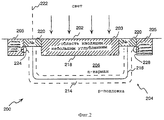
На фиг. 2 показано поперечное сечение одного из вариантов фотодиода 200 согласно настоящему изобретению, с сильнолегированной областью 220. Фотодиод 200 может быть частью чувствительного элемента изображения с КМОП-структурой, который может быть изготовлен при помощи современного процесса производства кремниевых КМОП-структур, такого как процесс, разработанный для производства микропроцессоров. Более того, чувствительный элемент изображения с КМОП-структурой может быть частью матрицы активных пиксельных чувствительных элементов изображения с КМОП-структурой, которая известна в данной области техники. Далее матрица активных пиксельных чувствительных элементов изображения с КМОП-структурой может использоваться в соединении с системой создания изображения, такой как цифровая видеокамера или видеоустройство. In FIG. 2 shows a cross section of one embodiment of a
Фотодиод 200, большей частью такой же, как и вариант фотодиода по фиг. 1, включает область кремниевой подложки 204, которая имеет проводимость первого типа, и область кармана 206, образованную в кремниевой подложке. Область кармана имеет проводимость второго типа. По описанному здесь одному из вариантов настоящего изобретения, область подложки 204 включает кремниевую подложку p-типа, а область кармана 206 включает кремниевый карман n-типа. Нужно понимать, что описанный здесь вариант настоящего изобретения также может быть реализован с использованием подложки n-типа и кармана p-типа. В одном из вариантов фотодиода согласно настоящему изобретению карман 206 может быть образован при помощи ионной имплантации подложки 204 или любых других хорошо известных процессов изготовления кармана. Photodiode 200, for the most part the same as the photodiode embodiment of FIG. 1 includes a region of a
Фотодиод 200 далее включает электроизолирующую область (диэлектрик) 202, которая образована наверху n-кармана 206. Эта диэлектрическая область прозрачна для света и позволяет свету проходить через нее. Диэлектрическая область 202 образована вытравливанием небольшого углубления наверху подложки. Небольшое углубление затем заполняется оксидом (SiO2), в результате чего образуется область изоляции небольшим углублением (показана штриховыми линиями, образующими острый угол с горизонтальным направлением). Небольшие углубления и процессы изготовления этих углублений хорошо известны специалистам.The
Небольшое углубление имеет ширину (в горизонтальном направлении), большую, чем ширина (в горизонтальном направлении) n-кармана 206, в результате чего оно покрывает область n-кармана 206. N-карман 206 определяется поверхностью n-кармана 216, которая ограничивает (отделяет) n-карман 206 от p-подложки 204. Когда n-карман и p-подложка находятся под напряжением обратного смещения, в поперечном направлении поблизости p-n-перехода образуется обедненная область диода. Если говорить более конкретно, обедненная область диода образуется в поперечном направлении поблизости поверхности 216 (первой поверхности), которая ограничивает n-карман 206 от подложки 204. После приложения подходящего напряжения обратного смещения к фотодиоду, как реакция на прошедший свет, упавший на область изоляции небольшим углублением, в обедненной области 214 диода может возбуждаться фототок. A small depression has a width (in the horizontal direction) greater than the width (in the horizontal direction) of the n-
Описанный здесь соответствующий настоящему изобретению вариант фотодиода 200 также включает сильнолегированную область (далее называемую защитным кольцом) 220, образованную в области изоляции небольшим углублением 202. Сильнолегированная область 220 имеет проводимость второго типа n, и, так как она сильно легирована, то обозначается как n+. Форма защитного кольца 220 может иметь тип любого замкнутого контура, который разделяет область изоляции небольшим углублением 202 на две области: внутреннюю область 203 и внешнюю область 205. По одному из вариантов согласно настоящему изобретению, область изоляции небольшим углублением 202 имеет прямоугольную форму, внутренняя область 203 имеет прямоугольную форму, а защитное кольцо 220 имеет округло-прямоугольную форму, как показано на фиг. 5 сопроводительных чертежей, рассматриваемой далее в этом описании.The embodiment of the
По одному из вариантов фотодиода 200 согласно настоящему изобретению, защитное кольцо 220 образовано в области изоляции небольшим углублением 202 путем вытравливания части этой области в первом положении, определенном пунктирной линией 222, и вокруг него. Защитное кольцо 220 образовано в вытравленной части. Защитное кольцо 220 затем подвергается процессу ионной имплантации для получения сильнолегированного защитного кольца 220. Первое положение 222 может определяться как положение, где поверхность 216, которая ограничивает n-карман 206 от подложки 204, встретилась бы с нижней поверхностью 218 области изоляции небольшим углублением 202, если бы защитное кольцо 220 в области изоляции небольшим углублением 202 не было образовано. Защитное кольцо 220, следовательно, образовано так, что поверхность 216 встречает (пересекает) нижнюю поверхность защитного кольца в положении, по существу, близком к первому положению. Предпочтительно, чтобы защитное кольцо 220 было образовано в области изоляции небольшим углублением 202 таким образом, чтобы поверхность 216 пересекала нижнюю поверхность защитного кольца посередине защитного кольца. In one embodiment of the
Наличие n+-легированного защитного кольца 220, в первом положении, приводит к тому, что обедненная область 214 граничит с областью изоляции небольшим углублением 202 на боковой внутренней поверхности 228 внешней области 205, расположенной напротив нижней поверхности 218 области изоляции небольшим углублением 202. Защитное кольцо 220, следовательно, определяет, каким образом обедненная область 214 контактирует с областью изоляции небольшим углублением 202. Завершение обедненной области 214 на боковой поверхности 228 области 202 более предпочтительно, чем завершение обедненной области 214 на нижней поверхности 218, так как определено, что боковая поверхность 228 является более чистой (например, она содержит меньше повреждений кремниевого кристалла и меньше остаточного продукта, чем нижняя поверхность 218 области изоляции небольшим углублением). Более чистая зона граничной поверхности, между обедненной областью 214 и поверхностью 228, обусловливает меньший уровень возникновения/рекомбинации дырок и электронов на граничной поверхности между обедненной областью и областью изоляции небольшим углублением и, следовательно, меньший уровень возникающего темнового тока. Более того, так как зона контакта 224, на боковой поверхности 228 обратно пропорциональна легированию защитного кольца, защитное кольцо 220 обусловливает меньшую зону контакта между обедненной областью 214 и областью изоляции небольшим углублением, чем в случае, когда обедненная область 214 пересекает нижнюю поверхность 218 области изоляции небольшим углублением.The presence of an n + doped
Защитное кольцо 220 отодвигает обедненную область от дна области изоляции небольшим углублением к ее боковой поверхности 228. Защитное кольцо 220 вызывает уменьшение зоны контакта между обедненной областью и областью изоляции небольшим углублением благодаря ретроградному легированию p-кармана, т. е. p-легирование выше находится ближе к поверхности. Таким образом, защитное кольцо 220 влияет на снижение темнового тока в варианте фотодиода согласно настоящему изобретению. The
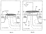
На фиг. 3a и 3b показаны частичные поперечные сечения одного из вариантов фотодиода согласно настоящему изобретению, на которых ширина защитного кольца является разной. Вариант, показанный на фиг. 3a, имеет защитное кольцо с шириной 350, которая меньше ширины 352 защитного кольца по варианту, показанному на фиг. 3b. Граничная поверхность между обедненной зоной 314 и боковой поверхностью 328 области изоляции небольшим углублением больше для защитного кольца с меньшей шириной 350 (фиг. 3а), чем для защитного кольца с большей шириной 352 (фиг. 3b). Соответственно, чем шире защитное кольцо, тем меньше зона граничной поверхности между обедненной областью и областью изоляции небольшим углублением и меньше темновой ток, возникающий вокруг этой зоны. In FIG. 3a and 3b show partial cross sections of one embodiment of a photodiode according to the present invention, in which the width of the protective ring is different. The embodiment shown in FIG. 3a has a guard ring with a width of 350 that is less than the
Хотя предпочтительными являются более широкие защитные кольца, из-за меньшей граничной поверхности на боковой поверхности 328 области изоляции небольшим углублением, чем шире защитное кольцо, тем меньше зона оптического восприятия, т. е. внутренняя область 303 области изоляции небольшим углублением. Соответственно, чем шире защитное кольцо, тем меньший темновой ток возникает, но из-за меньшей зоны оптического восприятия чувствительность диода снижается. Таким образом, для каждого конкретного процесса, оптимальная величина может быть определена, принимая во внимание чувствительность и темновой ток фотодиода. Although wider protective rings are preferred, due to the smaller boundary surface on the
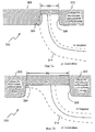
На фиг. 4а и 4b показаны первый и второй варианты фотодиода согласно настоящему изобретению. Защитное кольцо варианта по фиг. 4а фактически подобно защитному кольцу для варианта, описанного выше. Вариант по фиг. 4b имеет часть 407, определяющую внутреннюю часть 405 и внешнюю часть 403. Однако, вместо n+-сильнолегированного защитного кольца, между областями 403 и 405 образуется защитное кольцо 455 из затворного слоя оксида. Слой поликремниевого затвора 453, выше тонкой пленки оксида 461, образуется выше области изоляции небольшим углублением между внутренней и внешней областями 405 и 403 соответственно. Слой поликремния силицидируется и присоединяется к заземлению. Следует отметить, что кремниевая граничная поверхность в n-кармане разворачивается в обратную сторону, когда потенциал затвора составляет 0 вольт, и во время работы потенциал кармана является положительным. Обедненная область завершается на высококачественных областях затворного слоя оксида. Область затворного слоя оксида имеет высокое качество для обеспечения хорошего функционирования полевого МОП - транзистора.In FIG. 4a and 4b show first and second embodiments of a photodiode according to the present invention. The protective ring of the embodiment of FIG. 4a is actually similar to a guard ring for the embodiment described above. The embodiment of FIG. 4b has a
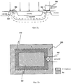
На фиг. 5а показано поперечное сечение варианта фотодиода согласно настоящему изобретению с металлическим контактом 560. N+-защитное кольцо также играет роль омического контакта для кармана фотодиода, так как n+-область является проводящей. Силицидированная область 562, наверху защитного кольца 520, также является проводящей и в типичном случае соединена с металлическим контактом 560, который подает напряжение смещения на фотодиод. Металлический контакт 560 соединен с пиксельным узлом 618, который показан далее на фиг. 6.In FIG. 5a shows a cross section of a variant of a photodiode according to the present invention with a
На фиг. 5b показана примерная компоновка КМОП - фотодиода согласно настоящему изобретению, показанного на фиг. 5а. Защитное кольцо 520 окружает внутреннюю фоточувствительную часть 503 фотодиода. N-карман включает часть, ограниченную пунктирной линией 512. Металлический контакт 560 контактирует с n+-защитным кольцом 520 для смещения фотодиода согласно настоящему изобретению.In FIG. 5b shows an exemplary arrangement of a CMOS photodiode according to the present invention shown in FIG. 5a. A
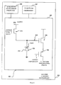
На фиг. 6 показан пример возможной реализации системы создания изображения 603, такой как цифровая видеокамера или видеоустройство, со схемой ячейки активного пиксельного чувствительного элемента 600, которая включает один вариант фотодиода 602, соответствующий настоящему изобретению. Ячейка активного пиксельного чувствительного элемента может быть включена в матрицу активных пиксельных чувствительных элементов с КМОП-структурой 605. Системы создания изображения 603 могут также включать устройство управления 607, соединенное с матрицей 605, и устройство последующей обработки 609, соединенное как с матрицей, так и с устройством управления 607. In FIG. 6 shows an example of a possible implementation of an
Ячейка активного пиксельного чувствительного элемента 600 включает установочный транзистор 614 и устройство истокового повторителя 616. Установочный транзистор 614 выборочно устанавливает пиксельный узел 618 на заранее определенное напряжение. Когда сигнал считывания поступил на переключающий транзистор строки 622, истоковый повторитель 616 обеспечивает напряжение, соответствующее напряжению в пиксельном узле 618, системе запечатления образа (не показана). Падающий свет вызывает падение напряжения пиксельного узла 618, обусловленное сбором электронов, фотогенерированных в обедненной области диода. Рассмотренный выше фотодиод 602, согласно настоящему изобретению включающий защитное кольцо, минимизирует отрицательный эффект темнового тока, так как этот ток существенно снижается рассмотренным выше защитным кольцом. The active
В изложенном выше описании изобретение было рассмотрено со ссылкой на его конкретные варианты реализации. Однако далее станет очевидным, что в нем могут быть сделаны различные модификации и изменения, не отступая от духа и объема изобретения, определяемых формулой изобретения. Описание и чертежи, соответственно, должны восприниматься в иллюстративном, а не в ограничительном смысле. Таким образом, объем изобретения должен ограничиваться только приложенной формулой изобретения. In the above description, the invention was considered with reference to its specific implementation options. However, it will further become apparent that various modifications and changes can be made therein without departing from the spirit and scope of the invention as defined by the claims. The description and drawings, respectively, should be understood in an illustrative rather than a restrictive sense. Thus, the scope of the invention should be limited only by the attached claims.
Claims (22)
Applications Claiming Priority (2)
| Application Number | Priority Date | Filing Date | Title |
|---|---|---|---|
| US08/941,800 US5859450A (en) | 1997-09-30 | 1997-09-30 | Dark current reducing guard ring |
| US08/941,800 | 1997-09-30 |
Publications (2)
| Publication Number | Publication Date |
|---|---|
| RU2178600C1 true RU2178600C1 (en) | 2002-01-20 |
| RU2000111514A RU2000111514A (en) | 2004-05-10 |
Family
ID=25477082
Family Applications (1)
| Application Number | Title | Priority Date | Filing Date |
|---|---|---|---|
| RU2000111514/28A RU2178600C1 (en) | 1997-09-30 | 1998-07-06 | Dark-current reducing ring |
Country Status (10)
| Country | Link |
|---|---|
| US (1) | US5859450A (en) |
| EP (1) | EP1034570B1 (en) |
| JP (1) | JP4309574B2 (en) |
| KR (1) | KR100371457B1 (en) |
| AU (1) | AU8291798A (en) |
| DE (1) | DE69833760T2 (en) |
| HK (1) | HK1029439A1 (en) |
| RU (1) | RU2178600C1 (en) |
| TW (1) | TW441119B (en) |
| WO (1) | WO1999017380A1 (en) |
Cited By (1)
| Publication number | Priority date | Publication date | Assignee | Title |
|---|---|---|---|---|
| RU2497319C1 (en) * | 2012-02-28 | 2013-10-27 | Федеральное государственное автономное образовательное учреждение высшего профессионального образования "Национальный исследовательский университет "Высшая школа экономики" | Printed-circuit board for spacecraft on-board radio-electronic equipment |
Families Citing this family (38)
| Publication number | Priority date | Publication date | Assignee | Title |
|---|---|---|---|---|
| KR100253372B1 (en) | 1997-12-08 | 2000-04-15 | 김영환 | Semiconductor device and fabricating method thereof |
| TW396645B (en) * | 1998-06-16 | 2000-07-01 | United Microelectronics Corp | Manufacturing method of CMOS sensor devices |
| US6545711B1 (en) * | 1998-11-02 | 2003-04-08 | Agilent Technologies, Inc. | Photo diode pixel sensor array having a guard ring |
| US6073343A (en) * | 1998-12-22 | 2000-06-13 | General Electric Company | Method of providing a variable guard ring width between detectors on a substrate |
| US6147366A (en) * | 1999-02-08 | 2000-11-14 | Intel Corporation | On chip CMOS optical element |
| US6445014B1 (en) * | 1999-06-16 | 2002-09-03 | Micron Technology Inc. | Retrograde well structure for a CMOS imager |
| US6310366B1 (en) * | 1999-06-16 | 2001-10-30 | Micron Technology, Inc. | Retrograde well structure for a CMOS imager |
| US6512401B2 (en) | 1999-09-10 | 2003-01-28 | Intel Corporation | Output buffer for high and low voltage bus |
| US7133074B1 (en) | 1999-09-28 | 2006-11-07 | Zoran Corporation | Image sensor circuits including sampling circuits used therein for performing correlated double sampling |
| US6465862B1 (en) * | 1999-10-05 | 2002-10-15 | Brannon Harris | Method and apparatus for implementing efficient CMOS photo sensors |
| US6627475B1 (en) | 2000-01-18 | 2003-09-30 | Taiwan Semiconductor Manufacturing Company | Buried photodiode structure for CMOS image sensor |
| US6194258B1 (en) | 2000-01-18 | 2001-02-27 | Taiwan Semiconductor Manufacturing Company | Method of forming an image sensor cell and a CMOS logic circuit device |
| DE10003472C1 (en) | 2000-01-27 | 2001-04-26 | Infineon Technologies Ag | Random number generator on IC with significantly improved independence of both signals |
| US6309905B1 (en) | 2000-01-31 | 2001-10-30 | Taiwan Semiconductor Manufacturing Company | Stripe photodiode element with high quantum efficiency for an image sensor cell |
| WO2001067518A1 (en) * | 2000-03-09 | 2001-09-13 | Koninklijke Philips Electronics N.V. | Solid state imaging sensor in a submicron technology and method of manufacturing and use of a solid state imaging sensor |
| US6365926B1 (en) | 2000-09-20 | 2002-04-02 | Eastman Kodak Company | CMOS active pixel with scavenging diode |
| KR20020096336A (en) * | 2001-06-19 | 2002-12-31 | 삼성전자 주식회사 | Cmos type image sensor |
| US20030049925A1 (en) * | 2001-09-10 | 2003-03-13 | Layman Paul Arthur | High-density inter-die interconnect structure |
| KR100454074B1 (en) * | 2001-12-26 | 2004-10-26 | 동부전자 주식회사 | Method of manufacturing image sensor for semiconductor device |
| US6534356B1 (en) | 2002-04-09 | 2003-03-18 | Taiwan Semiconductor Manufacturing Company | Method of reducing dark current for an image sensor device via use of a polysilicon pad |
| AU2002354316A1 (en) * | 2002-11-05 | 2004-06-07 | Akademia Gorniczo-Hutnicza | Monolithic active pixel dosimeter |
| US6818930B2 (en) | 2002-11-12 | 2004-11-16 | Micron Technology, Inc. | Gated isolation structure for imagers |
| KR100907884B1 (en) * | 2002-12-31 | 2009-07-15 | 동부일렉트로닉스 주식회사 | Semiconductor photodiode and manufacturing method thereof |
| US6897082B2 (en) * | 2003-06-16 | 2005-05-24 | Micron Technology, Inc. | Method of forming well for CMOS imager |
| KR100535924B1 (en) * | 2003-09-22 | 2005-12-09 | 동부아남반도체 주식회사 | CMOS Image sensor and its fabricating method |
| US7180049B2 (en) * | 2004-11-08 | 2007-02-20 | Taiwan Semiconductor Manufacturing Co., Ltd. | Image sensor with optical guard rings and method for forming the same |
| US7348651B2 (en) * | 2004-12-09 | 2008-03-25 | Taiwan Semiconductor Manufacturing Co., Ltd. | Pinned photodiode fabricated with shallow trench isolation |
| US7342268B2 (en) * | 2004-12-23 | 2008-03-11 | International Business Machines Corporation | CMOS imager with Cu wiring and method of eliminating high reflectivity interfaces therefrom |
| US7564083B2 (en) * | 2005-02-25 | 2009-07-21 | United Microelectronics Corp. | Active pixel sensor |
| EP1921685A4 (en) * | 2005-08-31 | 2014-12-17 | Fujitsu Semiconductor Ltd | Photo diode, solid imaging device, and their fabrication method |
| US8259293B2 (en) * | 2007-03-15 | 2012-09-04 | Johns Hopkins University | Deep submicron and nano CMOS single photon photodetector pixel with event based circuits for readout data-rate reduction communication system |
| US7598575B1 (en) | 2007-09-12 | 2009-10-06 | National Semiconductor Corporation | Semiconductor die with reduced RF attenuation |
| US8188578B2 (en) * | 2008-05-29 | 2012-05-29 | Mediatek Inc. | Seal ring structure for integrated circuits |
| US8815634B2 (en) * | 2008-10-31 | 2014-08-26 | Varian Semiconductor Equipment Associates, Inc. | Dark currents and reducing defects in image sensors and photovoltaic junctions |
| US8138531B2 (en) * | 2009-09-17 | 2012-03-20 | International Business Machines Corporation | Structures, design structures and methods of fabricating global shutter pixel sensor cells |
| US9171726B2 (en) * | 2009-11-06 | 2015-10-27 | Infineon Technologies Ag | Low noise semiconductor devices |
| JP5631668B2 (en) * | 2010-09-02 | 2014-11-26 | Nttエレクトロニクス株式会社 | Avalanche photodiode |
| KR101804268B1 (en) | 2010-11-02 | 2018-01-11 | 삼성전자주식회사 | Image sensor having guard ring and noise blocking area for blocking noise and Method for implementing the image sensor |
Family Cites Families (21)
| Publication number | Priority date | Publication date | Assignee | Title |
|---|---|---|---|---|
| JPS526097A (en) * | 1975-07-03 | 1977-01-18 | Moririka:Kk | Planar type photodiode |
| US4096622A (en) * | 1975-07-31 | 1978-06-27 | General Motors Corporation | Ion implanted Schottky barrier diode |
| US4137109A (en) * | 1976-04-12 | 1979-01-30 | Texas Instruments Incorporated | Selective diffusion and etching method for isolation of integrated logic circuit |
| US4261095A (en) * | 1978-12-11 | 1981-04-14 | International Business Machines Corporation | Self aligned schottky guard ring |
| US4414737A (en) * | 1981-01-30 | 1983-11-15 | Tokyo Shibaura Denki Kabushiki Kaisha | Production of Schottky barrier diode |
| US4691435A (en) * | 1981-05-13 | 1987-09-08 | International Business Machines Corporation | Method for making Schottky diode having limited area self-aligned guard ring |
| JPS58115873A (en) * | 1981-12-28 | 1983-07-09 | Fujitsu Ltd | Semiconductor light-receiving element |
| US4507853A (en) * | 1982-08-23 | 1985-04-02 | Texas Instruments Incorporated | Metallization process for integrated circuits |
| US4549914A (en) * | 1984-04-09 | 1985-10-29 | At&T Bell Laboratories | Integrated circuit contact technique |
| US4656732A (en) * | 1984-09-26 | 1987-04-14 | Texas Instruments Incorporated | Integrated circuit fabrication process |
| US4722910A (en) * | 1986-05-27 | 1988-02-02 | Analog Devices, Inc. | Partially self-aligned metal contact process |
| US5221856A (en) * | 1989-04-05 | 1993-06-22 | U.S. Philips Corp. | Bipolar transistor with floating guard region under extrinsic base |
| JPH036860A (en) * | 1989-06-02 | 1991-01-14 | Nec Corp | Solid state image pickup device |
| JP2661341B2 (en) * | 1990-07-24 | 1997-10-08 | 三菱電機株式会社 | Semiconductor light receiving element |
| JPH0582823A (en) * | 1991-09-20 | 1993-04-02 | Sharp Corp | Phototransistor |
| JPH0677452A (en) * | 1992-06-26 | 1994-03-18 | Nikon Corp | Solid-state image pickup device |
| US5438217A (en) * | 1994-04-29 | 1995-08-01 | General Electric Company | Planar avalanche photodiode array with sidewall segment |
| US5614744A (en) * | 1995-08-04 | 1997-03-25 | National Semiconductor Corporation | CMOS-based, low leakage active pixel array with anti-blooming isolation |
| US5841158A (en) * | 1996-03-01 | 1998-11-24 | Foveonics, Inc. | Low-stress photodiode with reduced junction leakage |
| JPH09321332A (en) * | 1996-05-31 | 1997-12-12 | Oki Electric Ind Co Ltd | Manufacture of semiconductor photo detector |
| JP2996943B2 (en) * | 1998-03-09 | 2000-01-11 | 株式会社東芝 | Semiconductor light receiving device and method of manufacturing the same |
-
1997
- 1997-09-30 US US08/941,800 patent/US5859450A/en not_active Expired - Fee Related
-
1998
- 1998-07-06 KR KR10-2000-7003432A patent/KR100371457B1/en not_active IP Right Cessation
- 1998-07-06 EP EP98933209A patent/EP1034570B1/en not_active Expired - Lifetime
- 1998-07-06 RU RU2000111514/28A patent/RU2178600C1/en not_active IP Right Cessation
- 1998-07-06 WO PCT/US1998/014024 patent/WO1999017380A1/en active IP Right Grant
- 1998-07-06 DE DE69833760T patent/DE69833760T2/en not_active Expired - Fee Related
- 1998-07-06 AU AU82917/98A patent/AU8291798A/en not_active Abandoned
- 1998-07-06 JP JP2000514343A patent/JP4309574B2/en not_active Expired - Fee Related
- 1998-07-14 TW TW087111407A patent/TW441119B/en not_active IP Right Cessation
-
2000
- 2000-12-29 HK HK00108568A patent/HK1029439A1/en not_active IP Right Cessation
Cited By (1)
| Publication number | Priority date | Publication date | Assignee | Title |
|---|---|---|---|---|
| RU2497319C1 (en) * | 2012-02-28 | 2013-10-27 | Федеральное государственное автономное образовательное учреждение высшего профессионального образования "Национальный исследовательский университет "Высшая школа экономики" | Printed-circuit board for spacecraft on-board radio-electronic equipment |
Also Published As
| Publication number | Publication date |
|---|---|
| US5859450A (en) | 1999-01-12 |
| KR100371457B1 (en) | 2003-02-07 |
| AU8291798A (en) | 1999-04-23 |
| JP2001518719A (en) | 2001-10-16 |
| TW441119B (en) | 2001-06-16 |
| EP1034570A4 (en) | 2002-09-25 |
| DE69833760D1 (en) | 2006-05-04 |
| DE69833760T2 (en) | 2006-09-07 |
| WO1999017380A1 (en) | 1999-04-08 |
| HK1029439A1 (en) | 2001-03-30 |
| KR20010030818A (en) | 2001-04-16 |
| JP4309574B2 (en) | 2009-08-05 |
| EP1034570B1 (en) | 2006-03-08 |
| EP1034570A1 (en) | 2000-09-13 |
Similar Documents
| Publication | Publication Date | Title |
|---|---|---|
| RU2178600C1 (en) | Dark-current reducing ring | |
| US6552320B1 (en) | Image sensor structure | |
| EP1032049B1 (en) | Photoelectric converting element | |
| US6169318B1 (en) | CMOS imager with improved sensitivity | |
| US5736756A (en) | Solid-state image sensing device with lght shielding film | |
| US20050064617A1 (en) | Buried, fully depletable, high fill factor photodiodes | |
| US5043783A (en) | Solid state image sensor | |
| US7368770B1 (en) | Well region with rounded corners | |
| JP2009534836A (en) | N-well barrier pixels that improve protection of dark reference columns and dark reference rows from blooming and crosstalk | |
| KR100780545B1 (en) | Cmos image sensor and method for manufacturing the same | |
| KR101256227B1 (en) | Image sensor | |
| US6545331B1 (en) | Solid state imaging device, manufacturing method thereof, and solid state imaging apparatus | |
| JPH05267695A (en) | Infrared image sensing device | |
| KR20020096336A (en) | Cmos type image sensor | |
| US8462239B2 (en) | Solid-state imaging device and electronic imaging device having multi-stage element isolation layer | |
| EP1109229A2 (en) | Buried, fully depletable, high fill factor photodiodes | |
| KR100333723B1 (en) | image sensor having on-transfer photodiode and data read out method of the same | |
| KR20040003981A (en) | Imase sensor with improved capability of protection against crosstalk and method for fabricating thereof | |
| JPH03261172A (en) | Solid state image sensor | |
| US7173299B1 (en) | Photodiode having extended well region | |
| KR100873293B1 (en) | Image sensor with improved protection of crosstalk | |
| KR100766675B1 (en) | A fabricating method of image sensor with decreased dark signal | |
| KR100531241B1 (en) | High sensitivity image sensor and fabrication method thereof | |
| KR100531231B1 (en) | High sensitivity image sensor and fabrication method thereof | |
| KR100736524B1 (en) | Image sensor |
Legal Events
| Date | Code | Title | Description |
|---|---|---|---|
| MM4A | The patent is invalid due to non-payment of fees |
Effective date: 20100707 |