KR960001175B1 - Manufacturing method of semiconductor device - Google Patents
Manufacturing method of semiconductor device Download PDFInfo
- Publication number
- KR960001175B1 KR960001175B1 KR1019870005761A KR870005761A KR960001175B1 KR 960001175 B1 KR960001175 B1 KR 960001175B1 KR 1019870005761 A KR1019870005761 A KR 1019870005761A KR 870005761 A KR870005761 A KR 870005761A KR 960001175 B1 KR960001175 B1 KR 960001175B1
- Authority
- KR
- South Korea
- Prior art keywords
- film
- semiconductor device
- silicon
- silicon oxide
- manufacturing
- Prior art date
Links
- 239000004065 semiconductor Substances 0.000 title claims description 108
- 238000004519 manufacturing process Methods 0.000 title claims description 25
- VYPSYNLAJGMNEJ-UHFFFAOYSA-N Silicium dioxide Chemical compound O=[Si]=O VYPSYNLAJGMNEJ-UHFFFAOYSA-N 0.000 claims description 52
- 229910052814 silicon oxide Inorganic materials 0.000 claims description 52
- 229910021420 polycrystalline silicon Inorganic materials 0.000 claims description 48
- 238000002955 isolation Methods 0.000 claims description 40
- 239000000758 substrate Substances 0.000 claims description 35
- 230000003647 oxidation Effects 0.000 claims description 31
- 238000007254 oxidation reaction Methods 0.000 claims description 31
- XUIMIQQOPSSXEZ-UHFFFAOYSA-N Silicon Chemical compound [Si] XUIMIQQOPSSXEZ-UHFFFAOYSA-N 0.000 claims description 28
- 229910052710 silicon Inorganic materials 0.000 claims description 28
- 239000010703 silicon Substances 0.000 claims description 28
- 238000000034 method Methods 0.000 claims description 27
- 229910052581 Si3N4 Inorganic materials 0.000 claims description 17
- HQVNEWCFYHHQES-UHFFFAOYSA-N silicon nitride Chemical compound N12[Si]34N5[Si]62N3[Si]51N64 HQVNEWCFYHHQES-UHFFFAOYSA-N 0.000 claims description 17
- 238000005530 etching Methods 0.000 claims description 9
- 230000001590 oxidative effect Effects 0.000 claims description 8
- 229920002120 photoresistant polymer Polymers 0.000 claims description 7
- 239000012535 impurity Substances 0.000 claims description 6
- 238000000151 deposition Methods 0.000 claims description 5
- 150000002500 ions Chemical class 0.000 claims description 4
- YCKRFDGAMUMZLT-UHFFFAOYSA-N Fluorine atom Chemical compound [F] YCKRFDGAMUMZLT-UHFFFAOYSA-N 0.000 claims description 3
- 229910052731 fluorine Inorganic materials 0.000 claims description 3
- 239000011737 fluorine Substances 0.000 claims description 3
- 238000007373 indentation Methods 0.000 claims 1
- 229910021421 monocrystalline silicon Inorganic materials 0.000 claims 1
- 230000001681 protective effect Effects 0.000 claims 1
- 238000000926 separation method Methods 0.000 description 15
- 239000013078 crystal Substances 0.000 description 5
- 238000001947 vapour-phase growth Methods 0.000 description 4
- 230000007547 defect Effects 0.000 description 3
- 239000000463 material Substances 0.000 description 3
- 230000002265 prevention Effects 0.000 description 3
- 238000000992 sputter etching Methods 0.000 description 3
- 230000015572 biosynthetic process Effects 0.000 description 2
- 238000007796 conventional method Methods 0.000 description 2
- 238000009413 insulation Methods 0.000 description 2
- XUKUURHRXDUEBC-SXOMAYOGSA-N (3s,5r)-7-[2-(4-fluorophenyl)-3-phenyl-4-(phenylcarbamoyl)-5-propan-2-ylpyrrol-1-yl]-3,5-dihydroxyheptanoic acid Chemical compound C=1C=CC=CC=1C1=C(C=2C=CC(F)=CC=2)N(CC[C@@H](O)C[C@H](O)CC(O)=O)C(C(C)C)=C1C(=O)NC1=CC=CC=C1 XUKUURHRXDUEBC-SXOMAYOGSA-N 0.000 description 1
- ZAMOUSCENKQFHK-UHFFFAOYSA-N Chlorine atom Chemical compound [Cl] ZAMOUSCENKQFHK-UHFFFAOYSA-N 0.000 description 1
- 241000293849 Cordylanthus Species 0.000 description 1
- 229910017855 NH 4 F Inorganic materials 0.000 description 1
- 230000001133 acceleration Effects 0.000 description 1
- XAGFODPZIPBFFR-UHFFFAOYSA-N aluminium Chemical compound [Al] XAGFODPZIPBFFR-UHFFFAOYSA-N 0.000 description 1
- 229910052782 aluminium Inorganic materials 0.000 description 1
- 229910052801 chlorine Inorganic materials 0.000 description 1
- 239000000460 chlorine Substances 0.000 description 1
- 239000004020 conductor Substances 0.000 description 1
- 238000011109 contamination Methods 0.000 description 1
- 238000001312 dry etching Methods 0.000 description 1
- 230000000694 effects Effects 0.000 description 1
- 238000010292 electrical insulation Methods 0.000 description 1
- 230000002452 interceptive effect Effects 0.000 description 1
- 238000000206 photolithography Methods 0.000 description 1
- 239000000126 substance Substances 0.000 description 1
Images


Classifications
-
- H—ELECTRICITY
- H01—ELECTRIC ELEMENTS
- H01L—SEMICONDUCTOR DEVICES NOT COVERED BY CLASS H10
- H01L21/00—Processes or apparatus adapted for the manufacture or treatment of semiconductor or solid state devices or of parts thereof
- H01L21/70—Manufacture or treatment of devices consisting of a plurality of solid state components formed in or on a common substrate or of parts thereof; Manufacture of integrated circuit devices or of parts thereof
- H01L21/71—Manufacture of specific parts of devices defined in group H01L21/70
- H01L21/76—Making of isolation regions between components
- H01L21/762—Dielectric regions, e.g. EPIC dielectric isolation, LOCOS; Trench refilling techniques, SOI technology, use of channel stoppers
- H01L21/76202—Dielectric regions, e.g. EPIC dielectric isolation, LOCOS; Trench refilling techniques, SOI technology, use of channel stoppers using a local oxidation of silicon, e.g. LOCOS, SWAMI, SILO
- H01L21/76213—Dielectric regions, e.g. EPIC dielectric isolation, LOCOS; Trench refilling techniques, SOI technology, use of channel stoppers using a local oxidation of silicon, e.g. LOCOS, SWAMI, SILO introducing electrical inactive or active impurities in the local oxidation region, e.g. to alter LOCOS oxide growth characteristics or for additional isolation purpose
- H01L21/76216—Dielectric regions, e.g. EPIC dielectric isolation, LOCOS; Trench refilling techniques, SOI technology, use of channel stoppers using a local oxidation of silicon, e.g. LOCOS, SWAMI, SILO introducing electrical inactive or active impurities in the local oxidation region, e.g. to alter LOCOS oxide growth characteristics or for additional isolation purpose introducing electrical active impurities in the local oxidation region for the sole purpose of creating channel stoppers
Abstract
내용 없음.No content.
Description
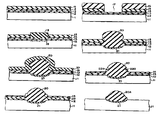
제1도(a) 내지 제1도(h)는 본 발명의 1실시예에 따른 반도체장치의 제조방법을 설명하기 위한 제조공정 단면도이다.1A to 1H are cross-sectional views of a manufacturing process for explaining a method of manufacturing a semiconductor device according to an embodiment of the present invention.
* 도면의 주요부분에 대한 부호의 설명* Explanation of symbols for main parts of the drawings
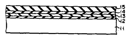
11 : 실리콘기판 12 : 제1실리콘 산화막11
13 : 다결정 실리콘막 14 : 제2실리콘 산화막13: polycrystalline silicon film 14: second silicon oxide film
15 : 실리콘 질화막 16 : 포토레지스트15
17 : 트인구멍 18 : 불순물 B+ 17: hole 18: impurity B +
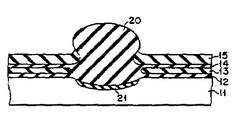
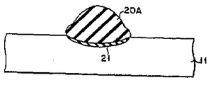
19 : 다결정 실리콘층 20 : 실리콘 산화막19
21 : 반전방지층 22 : 다결정 실리콘막21: inversion prevention layer 22: polycrystalline silicon film
22a : 다결정 실리콘부 23 : 실리콘 산화막22a: polycrystalline silicon portion 23: silicon oxide film
[산업상의 이용분야][Industrial use]
본 발명은 반도체장치의 제조방법에 관한 것으로, 특히 반도체기판상에 형성되는 반도체소자를 분리시키는 기술에 관한 것이다.BACKGROUND OF THE INVENTION 1. Field of the Invention The present invention relates to a method for manufacturing a semiconductor device, and more particularly, to a technique for separating a semiconductor device formed on a semiconductor substrate.
[종래의 기술 및 그 문제점][Traditional Technology and Problems]
최근, 반도체기판상에 형성되는 반도체소자를 분리시키는 기술로서는 LOCOS법(Local Oxidation of Silicon 法)이 널리 알려져 있는 바, 이 LOCOS법은 반도체기판상에 절연막을 매개하여 내산화성(耐酸化性) 막 예컨대 실리콘 질화막(SiN4막)을 형성하고 패터닝한 다음에 상기 내산화성 막을 마스크로 이용해서 선택적으로 산화시킴으로써, 두꺼운 반도체소자 분리용 절연막을 형성하는 것이다.Recently, the LOCOS method (Local Oxidation of Silicon method) is widely known as a technique for separating semiconductor devices formed on a semiconductor substrate. This LOCOS method is an oxidation resistant film formed by interfering an insulating film on a semiconductor substrate. For example, a silicon nitride film (SiN 4 film) is formed and patterned, and then selectively oxidized using the oxidized film as a mask, thereby forming a thick insulating film for semiconductor element separation.
그러나, 상술한 LOCOS법에서는 선택산화용 마스크재(즉, 내산화성 막)의 칫수와 형성된 반도체소자분리영역의 칫수간에 오차가 발생한다는 결점이 있다. 예컨대, 실리콘 질화막의 막두께를 2500Å로 하고, 반도체기판(실리콘기판)과 실리콘 질화막간의 절연막(실리콘 산화막)의 막두께를 1500Å, 선택 산화시의 반도체소자분리용 절연막의 두께를 8000Å으로 하여 반도체소자분리용 절연막을 막두께 5000Å∼6000Å으로 완성하면, 상술한 칫수의 오차는 0.8∼1.6㎛로 되게 된다. 이 때문에, LOCOS법을 이용하여 반도체소자를 전기적으로 분리시키기에 충분한 반도체소자분리용 절연막의 막두께를 얻고자 하는 경우, 반도체소자분리용 절연막의 실용적인 폭은 약 2.0㎛ 정도로 한정되게 된다. 따라서, 상술한 2.0㎛ 정도의 한계보다 좁은 반도체소자분리용 절연막을 얻고자 하는 경우에는 LOCOS법을 사용할 수 없다는 결점이 있다.However, the above-described LOCOS method has a drawback that an error occurs between the dimension of the selective oxidation mask material (i.e., the oxidation resistant film) and the dimension of the formed semiconductor element isolation region. For example, the film thickness of the silicon nitride film is set to 2500Å, the film thickness of the insulating film (silicon oxide film) between the semiconductor substrate (silicon substrate) and the silicon nitride film is 1500Å, and the thickness of the insulating film for semiconductor element isolation during selective oxidation is 8000Å. When the insulating film for separation is completed at a film thickness of 5000 kPa to 6000 kPa, the above-described error is 0.8 to 1.6 mu m. For this reason, when it is desired to obtain a film thickness of the semiconductor element isolation insulating film sufficient to electrically isolate the semiconductor element by using the LOCOS method, the practical width of the semiconductor element isolation insulating film is limited to about 2.0 mu m. Therefore, there is a drawback that the LOCOS method cannot be used to obtain an insulating film for semiconductor element separation narrower than the limit of about 2.0 μm.
또, 반도체소자분리영역의 폭과 형성되는 반도체소자분리용 절연막의 두께간에는 상관관계(相關關係)가 존재하고 있음이 실험적으로 확인되었는 바, 반도체소자분리영역의 폭을 좁게 하면 반도체소자분리용 절연막의 두께가 감소하여 전기적으로 충분한 반도체소자분리특성을 얻을 수 없게 된다는 문제점이 있다. 즉, 예컨대 상술한 조건하에서 반도체소자분리용 절연막을 1.4㎛의 폭으로 완성하는 경우, 반도체기판내에서 발생되는 결정결함을 고려하면 완성된 반도체소자분리용 절연막의 두께는 최대 약 3000Å∼3300Å 정도로 되는 바, 막두께가 3200Å 이상인 반도체소자분리용 절연막을 형성하는 것이 곤란하게 된다.In addition, it has been experimentally confirmed that there is a correlation between the width of the semiconductor device isolation region and the thickness of the semiconductor device isolation insulating film formed. When the width of the semiconductor device isolation region is narrowed, the insulating film for semiconductor device isolation is narrowed. There is a problem that it is impossible to obtain an electrically sufficient semiconductor device separation characteristics by reducing the thickness of. That is, for example, in the case where the insulating film for semiconductor device isolation is completed under the above-described conditions with a width of 1.4 占 퐉, the thickness of the completed semiconductor device isolation insulating film is about 3000 kPa to 3300 kPa in consideration of crystal defects occurring in the semiconductor substrate. It is difficult to form an insulating film for semiconductor element separation having a film thickness of 3200 GPa or more.
또한, 반도체소자분리용 절연막의 두께는 이 절연막밑에 형성되는 반전방지층 (conductivity reversion-preventing layer)의 불순물농도와의 상호관계로 결정되는 것으로서, 반전방지층의 불순물농도가 높아질수록 절연막의 두께가 두꺼워지게 되는데, 이렇게 반전방지층이 과도하게 높은 정도로 되는 경우에는 반도체 소자의 내성과 동작속도가 열화하기 때문에 반도체소자의 제조상 부적합하게 된다.In addition, the thickness of the insulating film for semiconductor element isolation is determined by the correlation between the impurity concentration of the conduction reversion-preventing layer formed under the insulation film, and as the impurity concentration of the inversion prevention layer increases, the thickness of the insulation film becomes thicker. However, if the anti-reversal layer becomes excessively high, the resistance and operating speed of the semiconductor element deteriorate, which makes the semiconductor device unsuitable for manufacturing.
상술한 바와 같이 LOCOS법을 이용하여 소자분리용 절연막을 형성하는 종래의 반도체장치의 제조방법에서는, 내산화성 막의 칫수와 형성된 반도체소자분리영역의 칫수간의 오차가 커지게 될 뿐만 아니라, 서로 분리되어야 하는 인접 반도체소자간의 소자분리영역의 폭이 좁은 경우에 충분히 두꺼운 반도체소자분리용 절연막을 형성할 수가 없다고 하는 결점이 있었다.As described above, in the conventional method of manufacturing a semiconductor device in which an insulating film for element isolation is formed by using the LOCOS method, the error between the dimension of the oxidation resistant film and the dimension of the formed semiconductor element isolation region is not only large, but must be separated from each other. There is a drawback that an insulating film for separating semiconductor elements thick enough cannot be formed when the width of the element isolation region between adjacent semiconductor elements is narrow.
[발명의 목적][Purpose of invention]
이에 본 발명은 상기와 같은 결정을 제거하기 위해 발명된 것으로, 좁은 폭의 반도체소자분리영역에서도 높은 정밀도로 두꺼운 반도체소자분리용 절연막을 형성할 수 있는 반도체장치의 제조방법을 제공하고자 함에 그 목적이 있다.Accordingly, the present invention has been invented to remove the crystal as described above, and an object thereof is to provide a method of manufacturing a semiconductor device capable of forming an insulating film for semiconductor device isolation with high precision even in a narrow semiconductor device isolation region. have.
[발명의 구성][Configuration of Invention]
상기 목적을 달성하기 위한 본 발명의 반도체장치의 제조방법은, 반도체기판상에 다결정 실리콘막을 퇴적형성하는 공정과, 상기 다결정 실리콘막상에 실리콘 산화막을 형성하는 공정, 상기 실리콘 산화막상에 내산화성 막을 형성하는 공정, 형성될 반도체소자분리영역에 대응하는 부분의 상기 내산화성 막을 선택적으로 제거하는 공정, 상기 잔존하는 내산화성 막을 마스크로 해서 상기 실리콘 산화막을 선택적으로 제거하는 공정, 상기 잔존하는 내산화성 막과, 상기 실리콘 산화막 및, 상기 내산화성 막을 선택적으로 제거하는 동안 상기 내산화성 막상에 도포되어 있는 포토레지스트를 마스크로 이용하여 상기 반도체기판내에 챈널스톱퍼를 형성하는데 사용되는 불순물을 이온주입하는 공정, 상기 포토레지스트를 제거한 후 상기 노출된 다결정 실리콘막상에 실리콘층을 선택적으로 성장시키는 공정, 상기 내산화성 막을 마스크로 해서 상기 실리콘층과 상기 다결정 실리콘막을 선택적으로 열산화시키는 공정, 상기 내산화성 막을 제거하는 공정, 반도체소자분리용 절연막의 측벽에 형성된 凹부를 실리콘 산화물로 매립하는 공정 및, 반도체소자영역이 형성될 부분의 반도체기판의 표면을 에칭에 의해 노출시키는 공정을 구비하여 이루어진 것을 특징으로 한다.A semiconductor device manufacturing method of the present invention for achieving the above object comprises the steps of depositing a polycrystalline silicon film on a semiconductor substrate, forming a silicon oxide film on the polycrystalline silicon film, and forming an oxidation resistant film on the silicon oxide film And selectively removing the oxidation resistant film in a portion corresponding to the semiconductor device isolation region to be formed, selectively removing the silicon oxide film using the remaining oxidation resistant film as a mask, and the remaining oxidation resistant film; Ion implanting impurities used to form a channel stopper in the semiconductor substrate using a photoresist applied on the oxidation resistant film as a mask while selectively removing the silicon oxide film and the oxidation resistant film, the photo The exposed polycrystalline seal after removing the resist Selectively growing a silicon layer on the cone film, selectively thermally oxidizing the silicon layer and the polycrystalline silicon film using the oxidizing film as a mask, removing the oxidizing film, and insulating sidewalls of the insulating film for semiconductor device isolation. And a step of embedding the formed trench with silicon oxide and exposing the surface of the semiconductor substrate in the portion where the semiconductor element region is to be formed by etching.
(작용)(Action)
상기와 같이 구성된 본 발명의 반도체장치에 제조방법에 의하면, 내산화성 막에 의해 측면이 둘러싸인 영역내에 형성된 실리콘층을 산화시키기 때문에 칫수오차를 극히 작게 할 수 있고, 또 반도체기판 자체가 거의 산화되지 않기 때문에 반도체기판의 결정결함 발생도 작게 할 수 있게 된다.According to the manufacturing method of the semiconductor device of the present invention configured as described above, since the silicon layer formed in the region surrounded by the oxidation resistant film is oxidized, the dimension error can be extremely small, and the semiconductor substrate itself is hardly oxidized. Therefore, the occurrence of crystal defects in the semiconductor substrate can also be reduced.
더우기, 반도체소자분리용 절연막으로 되는 실리콘층의 성장막두께를 적당하게 제거함으로써, 미세한 반도체소자분리영역에서도 반도체소자분리용 절연막의 두께를 용이하게 제어할 수 있게 되어 도체소자의 전기적 분리에 충분한 막두께를 얻을 수 있게 된다.Furthermore, by appropriately removing the growth film thickness of the silicon layer serving as the semiconductor device isolation insulating film, the thickness of the semiconductor device isolation insulating film can be easily controlled even in the minute semiconductor device isolation region, thereby sufficient film for electrical separation of the conductor device. The thickness can be obtained.
[실시예]EXAMPLE
이하, 도면을 참조해서 본 발명의 제1실시예를 상세히 설명한다.Hereinafter, a first embodiment of the present invention will be described in detail with reference to the drawings.
제1도(a) 내지 제1도(h)는 본 발명의 1실시예에 따른 반도체장치의 제조방법을 설명하기 위한 제조공정 단면도이다.1A to 1H are cross-sectional views of a manufacturing process for explaining a method of manufacturing a semiconductor device according to an embodiment of the present invention.
먼저, 제1도(a)에 나타낸 바와 같이 비저항이 1∼2Ω·cm이고 밀러 지주 (Miller index)가 (100)인 P형 실리콘기판(11)의 주표면을 온도가 1000℃인 O2분위기내에서 산화시킴으로써, 실리콘기판(11)의 표면보호용 제1실리콘 산화막(12)을 약 500Å의 막두께로 형성한다. 이어서, 이 실리콘 산화막(12)상에 기상성장법에 의해 막두께가 750Å인 다결정 실리콘막(13)을 퇴적형성한 다음에 이 다결정 실리콘막(13)의 표면을 온도가 1000℃인 O2분위기내에서 산화시킴으로써, 막두께가 500Å인 제2실리콘 산화막(14)을 형성한다. 계속해서, 기상성장법에 의해 제2실리콘 산화막(14)상에 막두께가 2000Å인 실리콘 질화막(15)을 퇴적형성한다.First, as shown in FIG. 1A, the main surface of the P-
이어서, 제11도(b)에 나타낸 바와 같이 불소가스를 이용한 리세스드 이온에칭 (recessed ion etching ; 이방성 식각법)에 근거한 사진식각법에 의해 포토레지스트 (16)를 마스크로 해서 반도체소자분리영역의 실리콘질화막(15)을 선택적으로 제거하고, 그후 잔존하는 실리콘 질화막(15)을 마스크로 해서 제2실리콘 산화막(14)을 제거함으로써, 트인구멍(開孔 ; 17)을 형성한다.Subsequently, as shown in FIG. 11 (b), the
다음으로, 제1도(c)에 나타낸 바와 같이 실리콘 질화막(15) 및 제2실리콘 산화막(14) 및 상기 포토레지스트(16)를 마스크로 해서 반도체소자분리영역으로 될 실리콘기판(11)의 부분에 다결정 실리콘막(13)과 제1실리콘 산화막(12)을 매개해서 반전방지를 위한 불순물(B+; 18)을 가속전압 100KeV에서 도우즈량 5×1012cm-3정도로 이온주입한다. 그후, 상기 포토레지스트(16)을 제거한 다음, 트인구멍(17)내에 노출된 다결정 실리콘막(13)의 표면상에만 선택 에피택셜성장법에 의해 다결정(또는, 단결정) 실리콘층(19)을 약 3000Å의 두께로 퇴적형성함으로써, 다결정 실리콘층(19)의 측벽(Side Wall)이 실리콘 질화막(15)에 접촉되도록 한다.Next, as shown in FIG. 1C, a portion of the
계속해서, 제1도(d)에 나타낸 바와 같이 실리콘 질화막(15)을 선택 산화용 마스크로 해서 온도가 1000℃인 H2+O2분위기내에서 다결정 실리콘층(19)과 그 밑의 다결정 실리콘막(13) 및 그 밑의 실리콘기판(11)을 선택적으로 산화시켜 실리콘기판(11)의 표면으로부터 약 250Å의 깊이까지 산화되도록 함으로써, 막두께가 8000Å인 반도체소자분리용 실리콘 산화막(반도체소자분리용 절연막 ; 20)을 형성한다. 이때, 상술한 공정에서는 실리콘기판(11)내에 이미 이온주입된 불순물(B+; 18)이 재확산되고 활성화되어 반전방지층(21)을 형성하게 된다.Subsequently, as shown in FIG. 1D, the
이어서, 제1도(e)에 나타낸 바와 같이 불소가스를 이용한 화학적 건식 에칭 (chemical dry etching ; 등방성 식각법)에 의해 불필요한 실리콘 질화막(15)을 선택적으로 제거한 다음, 기상성장법에 의해 반도체소자분리용 실리콘 산화막(20) 및 실리콘 산화막(14)상에 다결정 실리콘막(22)을 2000Å 정도의 막두께로 퇴적형성한다.Subsequently, as shown in FIG. 1 (e), the unnecessary
다음으로, 제1도(f)에 나타낸 바와 같이 염소계 가스를 이용한 리세스드 이온에칭에 의해 다결정 실리콘막(22)을 제거하게 되는데, 이 에칭이 이방성 에칭이므로 실리콘 질화막(15)을 제거할 때 반도체소자분리용 실리콘 산화막(20)의 측면쪽에 형성된 지붕형상(roof-shaped)의 凹부에만 다결정 실리콘부(22a)가 잔존하게 된다. 따라서, 지붕형상의 凹부(22a)가 채워지게 되므로 매끄러운 표면을 갖춘 반도체소자분리용 실리콘 산화막(20)을 형성할 수 있게 된다.Next, as shown in FIG. 1 (f), the polycrystalline silicon film 22 is removed by recessed ion etching using a chlorine-based gas. Since the etching is anisotropic etching, the semiconductor is removed when the
계속해서, 제1도(g)에 나타낸 바와 같이 온도가 1000℃인 O2분위기내에서 열산화를 행하여 반도체소자영역상에 잔존하는 다결정 실리콘막(13)을 전부 산화시킴으로써 실리콘 산화막(23)을 형성한다. 이때, 다결정 실리콘부(22a)는 다결정 실리콘막 (13)에 비해 막두께가 얇아질 뿐만 아니라 미세하게 되므로, 다결정 실리콘막(13)이 산화될 때 전체 다결정 실리콘부(22a)가 실리콘 산화막으로 변화되어 반도체소자분리용 실리콘 산화막(20)의 일부로 된다.Subsequently, as shown in FIG. 1 (g), thermal oxidation is performed in an O 2 atmosphere having a temperature of 1000 ° C. to oxidize all of the
이어서, 제1도(h)에 나타낸 바와 같이 반도체소자형성영역의 실리콘기판(11)이 노출될 때까지 NH4F용액에 의해 실리콘 산화막(14,23,12)을 제거하면, 반도체소자분리용 실리콘 산화막(20)의 두께가 실리콘 산화막(14,23,12)의 전체 두께와 다르기 때문에 반도체소자분리영역위에만 실리콘 산화막인 반도체소자분리용 실리콘 산화막 (20A)이 잔존하게 된다.Subsequently, as shown in FIG. 1 (h), when the
이후에는 통상적인 반도체장치의 제조방법에 의해 MOS트랜지스터 또는 바이폴러 트랜지스터 등과 같은 반도체소자를 형성하고, 예컨대 알루미늄배선에 의해 각 소자상호간에 접속시킴으로써 반도체장치를 완성하게 된다.Subsequently, a semiconductor device such as a MOS transistor or a bipolar transistor is formed by a conventional method of manufacturing a semiconductor device, and the semiconductor device is completed by connecting the elements to each other by, for example, aluminum wiring.
상술한 바와 같이 본 발명의 반도체장치의 제조방법은 실리콘 질화막(15)을 선택적으로 에칭하여 형성한 트인구멍내에 에피택셜성장법에 의해 다결정 실리콘층(19)을 형성하는 것을 특징으로 한다. 이러한 경우에는 다결정 실리콘층(19)의 측벽이 직접적으로 실리콘 질화막(15)에 접촉되게 되고, 그후 다결정 실리콘층(19)을 선택적으로 산화시켜 반도체소자분리용 실리콘 산화막인 반도체소자분리용 절연막(20)을 형성하게 된다. 이때에는 다결정 실리콘층(19)이 완전히 산화될 때까지 실리콘기판(11)이 산화되지 않는다. 따라서, LOCOS법을 이용할 때보다 소위 세부리형상(bird's beak)의 발생이 현저히 줄어들게 되므로, 반도체소자간에서는 완전한 전기적인 절연을 보장할 수 있도록 충분한 두께의 반도체소자분리용 산화막(20)을 형성할 수 있게 된다.As described above, the method for manufacturing a semiconductor device of the present invention is characterized in that the
또, 다결정 실리콘층(19)을 산화시킬 때 다결정 실리콘층(19)을 둘러싼 실리콘 질화막(15)은 산화되지 않는다. 따라서, 산화에 의한 다결정 실리콘층(19)의 체적증가로 인해 실리콘 질화막(15)내에 형성된 트인구멍(17)의 내벽(inner wall)이 옆으로 밀리지 않고, 상기 내벽이 윗쪽으로 돌출되게 된다. 그 결과, 다결정 실리콘층(19)의 산화전에 형성된 트인구멍(17)의 폭과 다결정 실리콘층(19)의 산화후에 형성된 반도체소자분리용 실리콘 산화막(20)의 폭간의 차이를 현저히 줄일 수 있게 된다.When the
또, 상기한 바와 같이 다결정 실리콘층(19)이 산화될 때 실리콘기판(11) 자체가 거의 산화되지 않게 되므로, 실리콘기판(11)은 다결정 실리콘층(19)의 산화에 의해 야기되는 체적팽창으로 인해 발생될 수 있는 기계적 응력(stress)을 받지 않게 된다. 또한, 반도체소자형성영역상에 퇴적형성되는 반도체소자간에서 완전한 전기적 절연을 확실하게 달성할 수 있으므로, 충분하게 두꺼운 반도체소자분리용 실리콘 산화막을 종래의 LOCOS법에 따른 결점에 구애받지 않고 형성할 수 있게 된다.In addition, since the
구체적으로는, 상술한 실시예에 의해 실현된 최소 반도체소자분리영역의 폭을 1.2㎛까지 줄일 수 있을 뿐만 아니라, 실리콘 산화막인 반도체소자분리용 절연막의 두께를 5000Å까지 크게 할 수 있게 된다. 따라서, 상기 막두께는 반도체소자를 전기적으로 분리시키기에 충분한 두께이고, 또 실리콘기판인 반도체기판의 결정결함은 반도체소자의 특성에 실질적으로 영향을 주지 않는 정도로 발생되며, 또 반도체소자분리용 절연막의 선택 산화용 마스크재(실리콘 산화막)의 설계치와 실질적으로 완성된 마스크재의 제조치의 오차는 0.2∼0.4㎛ 정도로 극히 작아진다는 것이 확인되었다.Specifically, the width of the minimum semiconductor device isolation region realized by the above-described embodiment can be reduced to 1.2 [mu] m, and the thickness of the semiconductor device isolation insulating film, which is a silicon oxide film, can be increased to 5000 kPa. Therefore, the film thickness is thick enough to electrically isolate the semiconductor elements, and crystal defects of the semiconductor substrate, which is a silicon substrate, are generated to a degree that does not substantially affect the characteristics of the semiconductor element, and It was confirmed that the error between the design value of the selective oxidation mask material (silicon oxide film) and the manufacturing value of the substantially completed mask material was as small as 0.2 to 0.4 m.
상술한 실시예에서는 반도체소자분리용 절연막을 형성하기 위해 다결정 실리콘막(22)을 퇴적형성하고 나서 이 다결정 실리콘막(22)을 리세스드 이온에칭처리하여 반도체소자분리용 실리콘 산화막(20)의 측벽의 凹부에만 다결정 실리콘부(22a)가 잔존하도록 했지만, 기상성장법에 의해 실리콘 산화막(도면중 참조부호 22에 대응)을 퇴적형성한 다음에 리세스드 이온에칭처리하여 반도체소자분리용 실리콘 산화막(20)의 측벽의 凹부에만 실리콘 산화부(도면중 참조부호 22a에 대응)가 잔존하도록 해도 된다. 또, 상술한 실시예에서는 실리콘기판의 표면에 그 기판의 표면보호용 실리콘 산화막(12)을 형성했지만, 실리콘기판의 다른 공정에서 오염 등의 영향을 거의 받지 않는 경우에는 이 공정은 불필요하게 된다.In the above-described embodiment, the polycrystalline silicon film 22 is deposited to form an insulating film for semiconductor device isolation, and the polycrystalline silicon film 22 is recessed ion etched to form sidewalls of the
[발명의 효과][Effects of the Invention]
이상 설명한 바와 같이 본 발명에 의하면, 좁은 폭의 반도체소자분리영역에서도 고정밀도로 두꺼운 반도체소자분리용 절연막을 형성할 수 있는 반도체장치의 제조방법을 제공할 수가 있게 된다.As described above, according to the present invention, it is possible to provide a semiconductor device manufacturing method capable of forming an insulating film for semiconductor element isolation with high precision even in a narrow semiconductor element isolation region.
Claims (11)
Applications Claiming Priority (3)
| Application Number | Priority Date | Filing Date | Title |
|---|---|---|---|
| JP133212 | 1986-06-09 | ||
| JP61133212A JPS62290146A (en) | 1986-06-09 | 1986-06-09 | Manufacture of semiconductor device |
| JP61-133212 | 1986-06-09 |
Publications (2)
| Publication Number | Publication Date |
|---|---|
| KR880001048A KR880001048A (en) | 1988-03-31 |
| KR960001175B1 true KR960001175B1 (en) | 1996-01-19 |
Family
ID=15099347
Family Applications (1)
| Application Number | Title | Priority Date | Filing Date |
|---|---|---|---|
| KR1019870005761A KR960001175B1 (en) | 1986-06-09 | 1987-06-08 | Manufacturing method of semiconductor device |
Country Status (3)
| Country | Link |
|---|---|
| US (1) | US4746625A (en) |
| JP (1) | JPS62290146A (en) |
| KR (1) | KR960001175B1 (en) |
Families Citing this family (13)
| Publication number | Priority date | Publication date | Assignee | Title |
|---|---|---|---|---|
| US4968640A (en) * | 1987-02-10 | 1990-11-06 | Industrial Technology Research Institute | Isolation structures for integrated circuits |
| US5019526A (en) * | 1988-09-26 | 1991-05-28 | Nippondenso Co., Ltd. | Method of manufacturing a semiconductor device having a plurality of elements |
| US5059550A (en) * | 1988-10-25 | 1991-10-22 | Sharp Kabushiki Kaisha | Method of forming an element isolating portion in a semiconductor device |
| JPH02162749A (en) * | 1988-12-15 | 1990-06-22 | Mitsubishi Electric Corp | Manufacture of semiconductor device |
| JPH0775243B2 (en) * | 1989-02-22 | 1995-08-09 | 株式会社東芝 | Method for manufacturing semiconductor device |
| US5002898A (en) * | 1989-10-19 | 1991-03-26 | At&T Bell Laboratories | Integrated-circuit device isolation |
| US5057463A (en) * | 1990-02-28 | 1991-10-15 | Sgs-Thomson Microelectronics, Inc. | Thin oxide structure and method |
| US5039625A (en) * | 1990-04-27 | 1991-08-13 | Mcnc | Maximum areal density recessed oxide isolation (MADROX) process |
| KR930011460B1 (en) * | 1991-01-22 | 1993-12-08 | 삼성전자 주식회사 | Isolation forming method of semiconductor |
| BR0205106A (en) | 2001-05-09 | 2003-06-17 | Shindengen Electric Mfg | Semiconductor device and its manufacturing method |
| ITMI20012010A1 (en) * | 2001-09-27 | 2003-03-27 | Getters Spa | SYSTEMS FOR THE CONVERSION OF WATER INTO HYDROGEN AND THE ABSORPTION OF HYDROGEN IN ELECTRONIC DEVICES AND PRODUCTION PROCESS |
| EP2306509A1 (en) * | 2009-09-29 | 2011-04-06 | STMicroelectronics Srl | Process for manufacturing an integrated device with "damascene" field insulation, and integrated device made by such process |
| EP2306508B1 (en) | 2009-09-29 | 2012-11-28 | STMicroelectronics Srl | Integrated device with raised LOCOS insulation regions and process for manufacturing such device |
Family Cites Families (5)
| Publication number | Priority date | Publication date | Assignee | Title |
|---|---|---|---|---|
| US4214946A (en) * | 1979-02-21 | 1980-07-29 | International Business Machines Corporation | Selective reactive ion etching of polysilicon against SiO2 utilizing SF6 -Cl2 -inert gas etchant |
| JPS57207348A (en) * | 1981-06-16 | 1982-12-20 | Fujitsu Ltd | Manufacture of semiconductor device |
| JPS5922344A (en) * | 1982-07-28 | 1984-02-04 | Fujitsu Ltd | Manufacture of semiconductor device |
| JPS59227137A (en) * | 1983-06-08 | 1984-12-20 | Nec Corp | Manufacture of semiconductor substrate |
| US4570325A (en) * | 1983-12-16 | 1986-02-18 | Kabushiki Kaisha Toshiba | Manufacturing a field oxide region for a semiconductor device |
-
1986
- 1986-06-09 JP JP61133212A patent/JPS62290146A/en active Granted
-
1987
- 1987-02-17 US US07/015,037 patent/US4746625A/en not_active Expired - Lifetime
- 1987-06-08 KR KR1019870005761A patent/KR960001175B1/en not_active IP Right Cessation
Also Published As
| Publication number | Publication date |
|---|---|
| JPH0565058B2 (en) | 1993-09-16 |
| JPS62290146A (en) | 1987-12-17 |
| KR880001048A (en) | 1988-03-31 |
| US4746625A (en) | 1988-05-24 |
Similar Documents
| Publication | Publication Date | Title |
|---|---|---|
| KR100278729B1 (en) | Method of forming electrical isolation structure in integrated circuit | |
| EP0113517B1 (en) | Method for forming an isolation region | |
| US3943542A (en) | High reliability, low leakage, self-aligned silicon gate FET and method of fabricating same | |
| KR960001175B1 (en) | Manufacturing method of semiconductor device | |
| EP0055521A1 (en) | Method of filling a groove in a semiconductor substrate | |
| US4295266A (en) | Method of manufacturing bulk CMOS integrated circuits | |
| US5100830A (en) | Method of manufacturing a semiconductor device | |
| US4876214A (en) | Method for fabricating an isolation region in a semiconductor substrate | |
| US4497108A (en) | Method for manufacturing semiconductor device by controlling thickness of insulating film at peripheral portion of element formation region | |
| US4721687A (en) | Method of increasing the thickness of a field oxide | |
| JPH0628282B2 (en) | Method for manufacturing semiconductor device | |
| US4054989A (en) | High reliability, low leakage, self-aligned silicon gate FET and method of fabricating same | |
| KR100246691B1 (en) | Fabrication method of semiconductor device | |
| EP0076147B1 (en) | Method of producing a semiconductor device comprising an isolation region | |
| KR0151267B1 (en) | Manufacturing method of semiconductor | |
| JPH04280451A (en) | Manufacture of semiconductor element isolating region | |
| JPH10308448A (en) | Isolation film of semiconductor device and formation method thereof | |
| KR900001059B1 (en) | Isolation method of semiconductor device | |
| KR940001813B1 (en) | Isolation method and device of semiconductor | |
| KR0161727B1 (en) | Element isolation method of semiconductor device | |
| KR100253268B1 (en) | Semiconductor element isolation method | |
| KR930005237B1 (en) | Manufacturing method of isolation regions in semiconductor | |
| KR920001732B1 (en) | Method of making semiconductor device | |
| JPH0467648A (en) | Manufacture of semiconductor device | |
| KR940003220B1 (en) | Making method for segregation area of semiconductor device |
Legal Events
| Date | Code | Title | Description |
|---|---|---|---|
| A201 | Request for examination | ||
| G160 | Decision to publish patent application | ||
| E701 | Decision to grant or registration of patent right | ||
| GRNT | Written decision to grant | ||
| FPAY | Annual fee payment |
Payment date: 20021231 Year of fee payment: 8 |
|
| LAPS | Lapse due to unpaid annual fee |