KR930010456B1 - Liquid crystal device and method of driving the same - Google Patents
Liquid crystal device and method of driving the same Download PDFInfo
- Publication number
- KR930010456B1 KR930010456B1 KR1019850006186A KR850006186A KR930010456B1 KR 930010456 B1 KR930010456 B1 KR 930010456B1 KR 1019850006186 A KR1019850006186 A KR 1019850006186A KR 850006186 A KR850006186 A KR 850006186A KR 930010456 B1 KR930010456 B1 KR 930010456B1
- Authority
- KR
- South Korea
- Prior art keywords
- liquid crystal
- voltage
- ferroelectric liquid
- value
- voltage signal
- Prior art date
Links
Images


Classifications
-
- G—PHYSICS
- G02—OPTICS
- G02F—OPTICAL DEVICES OR ARRANGEMENTS FOR THE CONTROL OF LIGHT BY MODIFICATION OF THE OPTICAL PROPERTIES OF THE MEDIA OF THE ELEMENTS INVOLVED THEREIN; NON-LINEAR OPTICS; FREQUENCY-CHANGING OF LIGHT; OPTICAL LOGIC ELEMENTS; OPTICAL ANALOGUE/DIGITAL CONVERTERS
- G02F1/00—Devices or arrangements for the control of the intensity, colour, phase, polarisation or direction of light arriving from an independent light source, e.g. switching, gating or modulating; Non-linear optics
- G02F1/01—Devices or arrangements for the control of the intensity, colour, phase, polarisation or direction of light arriving from an independent light source, e.g. switching, gating or modulating; Non-linear optics for the control of the intensity, phase, polarisation or colour
- G02F1/13—Devices or arrangements for the control of the intensity, colour, phase, polarisation or direction of light arriving from an independent light source, e.g. switching, gating or modulating; Non-linear optics for the control of the intensity, phase, polarisation or colour based on liquid crystals, e.g. single liquid crystal display cells
- G02F1/133—Constructional arrangements; Operation of liquid crystal cells; Circuit arrangements
-
- G—PHYSICS
- G09—EDUCATION; CRYPTOGRAPHY; DISPLAY; ADVERTISING; SEALS
- G09G—ARRANGEMENTS OR CIRCUITS FOR CONTROL OF INDICATING DEVICES USING STATIC MEANS TO PRESENT VARIABLE INFORMATION
- G09G3/00—Control arrangements or circuits, of interest only in connection with visual indicators other than cathode-ray tubes
- G09G3/20—Control arrangements or circuits, of interest only in connection with visual indicators other than cathode-ray tubes for presentation of an assembly of a number of characters, e.g. a page, by composing the assembly by combination of individual elements arranged in a matrix no fixed position being assigned to or needed to be assigned to the individual characters or partial characters
- G09G3/34—Control arrangements or circuits, of interest only in connection with visual indicators other than cathode-ray tubes for presentation of an assembly of a number of characters, e.g. a page, by composing the assembly by combination of individual elements arranged in a matrix no fixed position being assigned to or needed to be assigned to the individual characters or partial characters by control of light from an independent source
- G09G3/36—Control arrangements or circuits, of interest only in connection with visual indicators other than cathode-ray tubes for presentation of an assembly of a number of characters, e.g. a page, by composing the assembly by combination of individual elements arranged in a matrix no fixed position being assigned to or needed to be assigned to the individual characters or partial characters by control of light from an independent source using liquid crystals
- G09G3/3611—Control of matrices with row and column drivers
- G09G3/3648—Control of matrices with row and column drivers using an active matrix
- G09G3/3651—Control of matrices with row and column drivers using an active matrix using multistable liquid crystals, e.g. ferroelectric liquid crystals
-
- G—PHYSICS
- G02—OPTICS
- G02F—OPTICAL DEVICES OR ARRANGEMENTS FOR THE CONTROL OF LIGHT BY MODIFICATION OF THE OPTICAL PROPERTIES OF THE MEDIA OF THE ELEMENTS INVOLVED THEREIN; NON-LINEAR OPTICS; FREQUENCY-CHANGING OF LIGHT; OPTICAL LOGIC ELEMENTS; OPTICAL ANALOGUE/DIGITAL CONVERTERS
- G02F1/00—Devices or arrangements for the control of the intensity, colour, phase, polarisation or direction of light arriving from an independent light source, e.g. switching, gating or modulating; Non-linear optics
- G02F1/01—Devices or arrangements for the control of the intensity, colour, phase, polarisation or direction of light arriving from an independent light source, e.g. switching, gating or modulating; Non-linear optics for the control of the intensity, phase, polarisation or colour
- G02F1/13—Devices or arrangements for the control of the intensity, colour, phase, polarisation or direction of light arriving from an independent light source, e.g. switching, gating or modulating; Non-linear optics for the control of the intensity, phase, polarisation or colour based on liquid crystals, e.g. single liquid crystal display cells
- G02F1/133—Constructional arrangements; Operation of liquid crystal cells; Circuit arrangements
- G02F1/136—Liquid crystal cells structurally associated with a semi-conducting layer or substrate, e.g. cells forming part of an integrated circuit
- G02F1/1362—Active matrix addressed cells
- G02F1/1368—Active matrix addressed cells in which the switching element is a three-electrode device
-
- G—PHYSICS
- G09—EDUCATION; CRYPTOGRAPHY; DISPLAY; ADVERTISING; SEALS
- G09G—ARRANGEMENTS OR CIRCUITS FOR CONTROL OF INDICATING DEVICES USING STATIC MEANS TO PRESENT VARIABLE INFORMATION
- G09G3/00—Control arrangements or circuits, of interest only in connection with visual indicators other than cathode-ray tubes
- G09G3/20—Control arrangements or circuits, of interest only in connection with visual indicators other than cathode-ray tubes for presentation of an assembly of a number of characters, e.g. a page, by composing the assembly by combination of individual elements arranged in a matrix no fixed position being assigned to or needed to be assigned to the individual characters or partial characters
- G09G3/34—Control arrangements or circuits, of interest only in connection with visual indicators other than cathode-ray tubes for presentation of an assembly of a number of characters, e.g. a page, by composing the assembly by combination of individual elements arranged in a matrix no fixed position being assigned to or needed to be assigned to the individual characters or partial characters by control of light from an independent source
- G09G3/36—Control arrangements or circuits, of interest only in connection with visual indicators other than cathode-ray tubes for presentation of an assembly of a number of characters, e.g. a page, by composing the assembly by combination of individual elements arranged in a matrix no fixed position being assigned to or needed to be assigned to the individual characters or partial characters by control of light from an independent source using liquid crystals
- G09G3/3611—Control of matrices with row and column drivers
- G09G3/3648—Control of matrices with row and column drivers using an active matrix
- G09G3/3659—Control of matrices with row and column drivers using an active matrix the addressing of the pixel involving the control of two or more scan electrodes or two or more data electrodes, e.g. pixel voltage dependant on signal of two data electrodes
-
- G—PHYSICS
- G09—EDUCATION; CRYPTOGRAPHY; DISPLAY; ADVERTISING; SEALS
- G09G—ARRANGEMENTS OR CIRCUITS FOR CONTROL OF INDICATING DEVICES USING STATIC MEANS TO PRESENT VARIABLE INFORMATION
- G09G2300/00—Aspects of the constitution of display devices
- G09G2300/08—Active matrix structure, i.e. with use of active elements, inclusive of non-linear two terminal elements, in the pixels together with light emitting or modulating elements
- G09G2300/0809—Several active elements per pixel in active matrix panels
-
- G—PHYSICS
- G09—EDUCATION; CRYPTOGRAPHY; DISPLAY; ADVERTISING; SEALS
- G09G—ARRANGEMENTS OR CIRCUITS FOR CONTROL OF INDICATING DEVICES USING STATIC MEANS TO PRESENT VARIABLE INFORMATION
- G09G2310/00—Command of the display device
- G09G2310/02—Addressing, scanning or driving the display screen or processing steps related thereto
- G09G2310/0243—Details of the generation of driving signals
- G09G2310/0251—Precharge or discharge of pixel before applying new pixel voltage
-
- G—PHYSICS
- G09—EDUCATION; CRYPTOGRAPHY; DISPLAY; ADVERTISING; SEALS
- G09G—ARRANGEMENTS OR CIRCUITS FOR CONTROL OF INDICATING DEVICES USING STATIC MEANS TO PRESENT VARIABLE INFORMATION
- G09G3/00—Control arrangements or circuits, of interest only in connection with visual indicators other than cathode-ray tubes
- G09G3/20—Control arrangements or circuits, of interest only in connection with visual indicators other than cathode-ray tubes for presentation of an assembly of a number of characters, e.g. a page, by composing the assembly by combination of individual elements arranged in a matrix no fixed position being assigned to or needed to be assigned to the individual characters or partial characters
- G09G3/2007—Display of intermediate tones
- G09G3/2011—Display of intermediate tones by amplitude modulation
-
- Y—GENERAL TAGGING OF NEW TECHNOLOGICAL DEVELOPMENTS; GENERAL TAGGING OF CROSS-SECTIONAL TECHNOLOGIES SPANNING OVER SEVERAL SECTIONS OF THE IPC; TECHNICAL SUBJECTS COVERED BY FORMER USPC CROSS-REFERENCE ART COLLECTIONS [XRACs] AND DIGESTS
- Y10—TECHNICAL SUBJECTS COVERED BY FORMER USPC
- Y10S—TECHNICAL SUBJECTS COVERED BY FORMER USPC CROSS-REFERENCE ART COLLECTIONS [XRACs] AND DIGESTS
- Y10S359/00—Optical: systems and elements
- Y10S359/90—Methods
Abstract
내용 없음.No content.
Description
제1도는 본 발명의 실시예의 회로도.1 is a circuit diagram of an embodiment of the invention.
제2도는, 제5도, 제7도, 제8도, 제9도, 제11도, 제13도는 실시예의 구체적인 회로도.FIG. 2 is a schematic circuit diagram of the embodiment of FIGS. 5, 7, 8, 9, 11, and 13;
제3도, 제4도, 제6도, 제10도, 제12도, 제14도, 제15도는 구동파형을 나타낸 도면.3, 4, 6, 10, 12, 14, and 15 show driving waveforms.
제16도는 실시예의 단면도.16 is a cross-sectional view of an embodiment.
제17도는 시험용 소자의 단면도.17 is a sectional view of a test device.
제18도, 제19도, 제20도, 제21도는 강유전성 액정의 기본특성도.18, 19, 20, and 21 are basic characteristics of ferroelectric liquid crystals.
본 발명은 액정소자에 관한 것이며, 특히 쌍안정성(雙安定性)을 가진 강유전성 액정(强誘電性 液晶)을 조합한 액정th자와 그 구동방법에 관한 것이다.BACKGROUND OF THE
액정소자는 디스플레이, 광셔터, 편광기(偏光器)등에 사용되고 있지만, 특히 액티브매트릭스 디스플레이는 표시부에 박막트랜지스터(TFT) 등의 스위치소자를 형성하고, 액정 등의 전기광학특성을 가진 물질을 적층한 디스플레이이며, 다주사선이고 고도로 정밀하고, 큰 면적에 사용하는 디스플레이에 적합한 방식이다. TN 액정이나 게스트호스트액정 등 광투과특성이 인가전압의 실효치에 의존하는 액정과 TPT를 적층한 액티브매트릭스를 형성할 경우에는, TFT의 오프저항 Roff이 충분히 크고, 온저항 Ron이 충분히 작으며, 액정자체희 전류리크에 의한 시정수(時定數)가 충분히 클 경우에는, 주사선수가 많은 디스플레이가 형성가능하지만, 상기 각 파라미터중 하나라도 불충분한 것이 있으면 특성이 양호한 디스플레이를 형성할 수 없다.Liquid crystal devices are used in displays, optical shutters, polarizers, etc. In particular, active matrix displays are formed by forming switch elements such as thin film transistors (TFTs) on the display, and laminating materials having electro-optic characteristics such as liquid crystals. It is a multiscan, highly precise, and suitable for large area displays. In the case of forming an active matrix in which a liquid crystal having a light transmission characteristic such as a TN liquid crystal or a guest host liquid crystal depends on the effective value of an applied voltage and a TPT layer, the TFT has a large off resistance R off and a large on resistance R on . When the time constant due to current leakage by the liquid crystal itself is sufficiently large, a display with many scanning players can be formed, but if any one of the above parameters is insufficient, a display with good characteristics cannot be formed. .
TN 액정 등, 표시상태가 인가전압의 실효치에 의존하는 액정을 사용한 액티브매트릭스 디스플레이의 구동특성은 본 발명자들이 1983년, 일본국 텔레비전학회 전국대회 예고집(豫稿集) 121-122 페이지에 발표되어 있다.The driving characteristics of an active matrix display using a liquid crystal whose display state depends on the effective value of applied voltage, such as a TN liquid crystal, are disclosed by the inventors in 1983, Proceedings of the National Television Society of Japan, pages 121-122. have.
이 결과를 보면, 박막트랜지스터(TFT)등의 스위치소자의 오프저항 Roff을 파라미터로 하여 액정층에 인가되는 전압파형을 계산하면, 표시가능한 조건은 선택전압의 실효치 Vs, 비선택전압의 실효치 Vns로 하여Vs>Vns이며, 스위치소자의 오프저항이 클수록 앙호한 표시특성이 얻어진다는 것을 알 수 있다. 그러므로, TN 액정을 액티브매트릭스 디스플레이에 사용할 경우에는 스위치소자의 오프저항 Roff을 충분히 크게하는 방향으로 개량되고 있다.In this result, a thin film transistor (TFT) when the off-resistance R off of the switching element, such as a parameter calculating the voltage waveform applied to the liquid crystal layer, visible conditions of the selection voltage effective value V s, the effective value of the non-selection voltage and to V s> V ns ns to V, it can be seen that the greater the off-resistance angho a display characteristic of the switching element thus obtained. Therefore, when the TN liquid crystal is used in an active matrix display, it is improved in a direction in which the off resistance R off of the switch element is sufficiently increased.
그러나, 예를 들면 디스플레이를 조명하기 위한 광원의 광작용에 의해 TFT 소자의 오프저항이 저하되어버리는 현상 등이 알려져 있다. 이것에 대해, 비정질실리큰 TFT에서는 채널부에 입사하는 광을 차단하기위한 금속막을 적층하는 방법이나, 다결정실리콘 TFT에서는 소자구조를 바꾸는 방법 등에 의해 오프저항 Roff을 크게 유지하는 것이 제안되어 있으나, 소자의 제조공정이 복잡해진다는 것, 또는 강렬한 광에 대해서는 오프저항 Roff의 저하를 피할 수 없을 정도로 액티브매트릭스용의 스위치소자의 특성으로서 충분한 것이라고는 할 수 없는 현상이다.However, for example, a phenomenon in which the off resistance of a TFT element is lowered due to light action of a light source for illuminating a display is known. On the other hand, in the amorphous silicon TFT, it is proposed to keep the off resistance R off large by laminating a metal film for blocking light incident on the channel portion, or changing the device structure in the polysilicon TFT. This is a phenomenon that the manufacturing process of the device is complicated or that the characteristics of the switch element for the active matrix are not enough to inevitably reduce the off resistance R off for intense light.
또, 액정자체가 메모리성을 가진 강유전액정이 클라크(N.A Clark) 등에 의해 발표(Applied Physics Letter 36(11), 899-901 페이지, 또는 Molecular Crystal & Liquid Crystal Vol 94, 213∼234 페이지, 또는 일본국 특개소 56-107216호 등)되어 있으나, 실제의 디스플레이에 응용하는 경우의 검토는 충분하다고 할 수 없다.In addition, the ferroelectric liquid crystals in which the liquid crystal itself is memory-released are published by Clark et al. (Applied Physics Letter 36 (11), pages 899-901, or Molecular Crystal & Liquid Crystal Vol 94, pages 213-234, or Japan). Japanese Patent Application Laid-Open No. 56-107216, etc., but it is not sufficient to examine the case of applying it to an actual display.
본 발명의 목적은 쌍안정성을 가진 강유전성 액정을 액티브매트릭스에 사용하여, 다주사선이며 정보량이 많은 액정소자를 구성하기 위한 소자구성 및 그 구동방법을 제공하는데 있다.SUMMARY OF THE INVENTION An object of the present invention is to provide a device configuration and a driving method for forming a liquid crystal device having a multi-scanning line and a large amount of information by using a bistable ferroelectric liquid crystal in an active matrix.
본 발명은 강유전성 액정에 발견되어 있는 메모리특성, 나아가서는 본 발명자가 실험에 의해 발견한 여러현상을 이용하여, 액티브매트릭스 액정소자 및 그 구동방법을 구성하는 것이다.The present invention uses the memory characteristics found in ferroelectric liquid crystals, and furthermore, the active matrix liquid crystal element and its driving method using the various phenomena found by the experimenter.
상기 목적을 달성하는 본 발명의 액정소자의 구동방법의 제1의 특징으로 하는 것은 표시전극간에 쌍안정성을 가진 강유전성 액정을 협지하여 이루어지고, 복수의 주사전극과 복수의 신호전극과의 각각의 교점에 스위치소자를 설치하고, 상기 각 스위치소자와 상기 표시전극의 한쪽과의 접속점에 제어소자를 설치한 액정소자의 구동방법에 있어서, 상기 스위치소자가 오프일 때 파고치(波高値)의 절대치가 상기 강유전성 액정의한 계치( |Vth| ) 미만으로 유지되는 전압을 상기 강유전성 액정에 인가하고 상기 스위치소자가 온일 때 파고치의 절대치가 상기 한계치( |Vth| ) 미만인 제1의 전압신호를 상기 강유전청 액정에 인가하여, 광투과상태를 유지시키고 상기 스위치소자가 온일 때 파고치의 절대치가 상기 한계치 ( |Vth| ) 이상인 제2의 전압신호를 상기 강유전성 액정에 인가하여, 광투과상태를 변화시키는 단계로 이루어지는 것에 있다.A first feature of the method for driving the liquid crystal element of the present invention, which achieves the above object, is obtained by sandwiching a ferroelectric liquid crystal having bistable stability between display electrodes, and each intersection between a plurality of scan electrodes and a plurality of signal electrodes. In the method of driving a liquid crystal element in which a switch element is provided in the switch element, and a control element is provided at a connection point between each switch element and one of the display electrodes, an absolute value of the crest value when the switch element is turned off. The first voltage signal whose absolute value of crest value is less than the limit value (| V th |) is applied to the ferroelectric liquid crystal when a voltage maintained below the threshold (| V th |) of the ferroelectric liquid crystal is applied to the ferroelectric liquid crystal. the voltage signal of the second or higher is applied to the ferroelectric liquid crystal to blue, maintaining the light transmitting state and the absolute value of wave height when the switch element is on the limit values (| | V th) It is applied to the ferroelectric liquid crystal group, and being made of a step of changing the light transmitting state.
본 발명의 액정소자의 구동방법의 제2의 특징으로 하는 것은 표시전극간에 쌍안정성을 가진 강유전성 액정을 협지하여 이루어지고, 복수의 주사전극과 복수의 신호전극과의 각각의 교점에 스위치소자를 설치하고 상기 각 스위치소자와 상기 표시전극의 한쪽과의 접속점에 제어소자를 설치한 액정소자의 구동방법에 있어서, 상기 스위치소자가 오프일 때 파고치의 절대치가 상기 강유전성 액정의 한계치 ( |Vth| ) 미만으로 유지되는 전압을 상기 강유전성 액정에 인가하고 상기 스위치소자가 온일 때 파고치의 절대치가 상기 한계치( |Vth| ) 미만인 제1의 전압신호를 상기 강유전성 액정에 인가하여, 광투과상태를 유지시키고, 상기 스위치소자가 온일 때 파고치의 절대치가 상기 한계치 ( |Vth| ) 이상인 고정의 값의 제2의 전압신호를 상기 강유전성 액정에 인가하여, 광투과상태를 소정의 상태로 하고, 파고치의 절대치가 상기 한계치 ( |Vth| ) 이상이고, 또한 상기 제2의 전압신호와는 역극성(逆極性)의 제3의 전압신호를 상기 강유전성 액정에 인가하여, 광투과상태를 변화시키는 단계로 이루어지는 것에 있다.A second feature of the method for driving a liquid crystal element of the present invention is to sandwich a ferroelectric liquid crystal having bistable stability between display electrodes, and to provide a switch element at each intersection of a plurality of scan electrodes and a plurality of signal electrodes. In the method for driving a liquid crystal element provided with a control element at a connection point between each switch element and one of the display electrodes, the absolute value of the crest value when the switch element is off is the limit value (| V th |) of the ferroelectric liquid crystal. A voltage maintained below is applied to the ferroelectric liquid crystal, and when the switch element is on, a first voltage signal whose absolute value of crest value is less than the limit value (| V th |) is applied to the ferroelectric liquid crystal to maintain a light transmission state. , the switching element, the absolute value is the threshold value when the wave height is on (| V th |) is greater than or equal to the voltage signal of the second value of the fixed ferroelectric liquid The application to the light transmitting state to a predetermined state, and the absolute value of digging the threshold value (| V th |) or higher, and also the voltage signal of the third of the second voltage signal with an inverse polarity (逆極性) of Is applied to the ferroelectric liquid crystal to change the light transmission state.
본 발명의 액정소자의 특징으로 하는 것은 표시전극간에 쌍안전성을 가진 강유전성 액정을 협지하여 이루어지는 액정소자에 있어서, 복수의 주사전극과 복수의 신호전극과의 각각의 교점에 스위치소자를 설치하고, 상기 각 스위치소자와 상기 표시전극의 한쪽과의 접속접에, 상기 스위치소자가 오프일 때 상기 강유전성 액정에 인가되는 전압의 파고치의 절대치가 상기 강유전성 액정의 한계치 ( |Vth| ) 미만으로 유지되는 제어소자를 설치하고, 상기 스위치소자는 제어단자가 상기 주사전극에, 한쪽 주단자가 상기 신호전극에, 다른쪽 주단자가 상기 표시전극외 한쪽에 접속되는 3단자스위치소자인 것에 있다.The liquid crystal device of the present invention is characterized in that a liquid crystal device is formed by sandwiching a ferroelectric liquid crystal having bi-stability between display electrodes, wherein a switch element is provided at each intersection of a plurality of scan electrodes and a plurality of signal electrodes. Control at which the peak value of the voltage applied to the ferroelectric liquid crystal when the switch element is turned off is maintained below the limit value (| V th |) of the ferroelectric liquid crystal at the contact between each switch element and one of the display electrodes. An element is provided, wherein the switch element is a three-terminal switch element in which a control terminal is connected to the scan electrode, one main terminal is connected to the signal electrode, and the other main terminal is connected to one other than the display electrode.
다음에, 본 발명의 실시예에 대하여 도면에 따라서 상세히 설명한다.Next, embodiments of the present invention will be described in detail with reference to the drawings.
본 발명은 본 발명자들이 발견한 다음에 기술차는 실험사실에 의거한 것이다.The present invention is based on the findings of the present inventors, and then the technical difference.
먼저, 실험소자의 구성에 대하여 제17도에 따라서 설명한다.First, the configuration of the experimental element will be described with reference to FIG.
액정소자는 투면전극(18)을 가진 유지, 플라스틱 등의 2매의 투명기판(17), PET(폴리에틸렌 테레프탈레이트) 필름스페이서(19), 강유전성(强誘電性) 액정(20)으로 이루어진다. 투명기판(17)의 한쪽은 포토레지스트와 플루오르화수소산 용액을 사용하여 에칭하고, 제17도에 나타낸 것과 같이 스텝부를 형성해 놓았다. 이와 같은 스텝부를 형성하면, 두께가 2rμ 이하의 필름의 입수가 곤란함에도 불구하고, 2㎛ 이하의 갭(gap)의 액정소자를 안정되게 제작할 수 있다. 강유전성 액정으로서는 제1표에 나타낸 4성분 혼합재료를 사용했다. 갭은 1.6㎛으로 하고, 투명전극(18)상에는 배향막(配向膜)의 도포, 러빙 등의 표면처리는 일체하지 않았다.The liquid crystal element is composed of two
[표 1]TABLE 1

다음에, 액정분자의 배향방향을 기술한다. 먼저, 액정상(液晶相)ㆍ등방상(等方相) 전이온도보다 약간 높은 온도(이 경우는 120℃정도)까지 가열하여 일단 등방상으로 한다음, 0.1℃/분 정도로 서냉(徐冷)하여 스맥틱 A상(분자장축이 층면에 수직)으로 했다. 이 때. 액정은 셀측면(액정ㆍ스페이서필름계면)에서의 계면효과에 의해 분자장축이 이 계면에 평행으로 또한 층이 수직으로 줄지으면서 성장해 간다. 드디어, 측정에 충분한 영역에 있어서, 양호한 모노도메인을 형성한다. 모노도메인 성장과정게 있어서는, 분자장축과 층법선이 서로 수직인 스멕틱 A상을 형성하지만, 다시 54℃ 이하까지 서냉하면, 층의 평면성을 유지하면서 분자장축이 층법선으로부터 경사진 스멕틱C*상으로 된다. 본 발명에 있어서 소자에 나선이 소실되어 쌍안정성이 출현하고 있는 것을 다음에 기술하는 관찰에 의해 확인했다.Next, the orientation direction of liquid crystal molecules is described. First, it is heated to a temperature slightly higher than the liquid crystal phase and isotropic transition temperature (in this case, about 120 ° C.) to make it isotropic once, and then slowly cooled to about 0.1 ° C./min. To the Smactic A phase (molecular axis axis perpendicular to the layer surface). At this time. The liquid crystal grows while the molecular long axis is parallel to this interface and the layer is vertically reduced by the interface effect at the cell side (liquid crystal and spacer film interface). Finally, a good monodomain is formed in a region sufficient for measurement. In the monodomain growth process, the Smectic A phase in which the molecular axis and the layer normal form perpendicular to each other is formed, but when cooled slowly to 54 ° C. or lower, the Smectic C * inclined from the layer normal while maintaining the planarity of the layer. It becomes a phase. In the present invention, it was confirmed by observation described below that the spiral disappeared in the device and the bistable stability appeared.
소장에의 인가전압파형과 소자의 광투과율(이하 밝기라고 표현함)의 관계의 측정결과를 설명한다. 이들 전기광학특성의 측정은 광강도 검출기를 부착한 편광현미겅 직교 니콜프리즘(Nicol prism)하에서 파장이 550nm의 단색광원을 사용하여 행하고 시료온도는 실온 23℃로 했다. 분자배향의 쌍안정선 때문에 이 액정에서는 전기광학적인 메모리성(본 발명자들은 전계제거 후도 수개월이상 기억하는 것을 확인했음)이 출현하여, 제18도에 나타낸 것과 같이 앞에 인가한 펄스와 역극성의 펄스를 인가했을 때에 비로서 명암(明暗)의 광투과상태가 역전했다. 액정에 인가되는 전압의 펄스의 극성을 앞에 인가한 펄스와 동일하게 한 경우는 밝기는 변하지 않는다. 명암의 광투과상태를 완전히 역전할 수 있는 충분한 폭(시간폭을 가리킴)과 파고치(波高値)를 가진 전압펄스를 인가한다음 동일폭으로 역극성의 전압펄스(파고치를 VLC로 나타냄)를 인가할 경우, VLC의 절대치가 어떤 값 이하(0도 포함)에서는 광학응답은 일어나지 않는다. 본 발명에서는 광학응답이 일어나기 시작하는 한계치전압을, VLC>0틴 경우를 Vth (+), VLC<0인 경우를 Vth (-)로 정의한다. 또한. -Vth (-)<VLC<Vth (+)인 전압대를 불감대로 정의한다. 액정에의 인가전압의 절대치 |VLC|를 Vth (+)이상, 또는 Vth (-)이상으로 하면, 그 전압치가 클수록 밝기 B의 변화량은 크다. 그러나, 밝기 B에는 포화치 Vsat (+), Vsat (-)가 존재하며, 어떤 전압치이상에서는 전압의존이 없어진다.The measurement results of the relationship between the voltage waveform applied to the small intestine and the light transmittance (hereinafter referred to as brightness) of the device will be described. The measurement of these electro-optical characteristics was carried out using a monochromatic light source having a wavelength of 550 nm under a polarization microscope orthogonal Nicol prism with a light intensity detector, and the sample temperature was set at 23 ° C. Because of the bistable line of molecular orientation, electro-optic memory (the inventors have confirmed that they remember more than a few months after removing the electric field) appears in this liquid crystal, and the pulse applied in reverse and the reverse polarity as shown in FIG. When light was applied, the light transmission state of light and shade reversed. In the case where the polarity of the pulse of the voltage applied to the liquid crystal is made the same as the pulse applied previously, the brightness does not change. Apply a voltage pulse with a sufficient width (pointing time) and crest value to completely reverse the light transmission of the contrast, and then apply a reverse polarity voltage pulse (peak value as V LC ). When is applied, the optical response does not occur when the absolute value of V LC is below a certain value (including 0). In the present invention, the threshold voltage at which the optical response starts to occur is defined as V th (+) for V LC > 0 and V th (−) for V LC <0. Also. A voltage band with -V th (-) <V LC <V th (+) is defined as deadband. When the absolute value | V LC | of the applied voltage to the liquid crystal is set to V th (+) or more or V th (−) or more, the larger the voltage value, the larger the amount of change in brightness B. However, saturation values V sat (+) and V sat (-) exist in brightness B, and voltage dependence is no longer above a certain voltage value.
제19c도는 제19a도에 나타낸 2개의 전압펄스를 인가한 경우의 밝기(제19b도)의 측정에서 얻은 것이다. 즉, 인가신호중 앞의 전압펄스(파고치 V1)로 밝기의 초기치 Bo를 정한다. 이 때, V1이 플러스이고 충분히 크면 밝기의 초기치 Bo는 최대치 Bmax이며, 제2의 전압펄스(파고치 V2)를 횡축으로 한 그래프(제19c도)에 있어서의 실선(c)의 특성으로 된다. 또, V1이 마이너스이고 충분히 크면, 밝기의 초기치 Bo가 Bmin으로 되고, V1에 대한 특성픈 제19도(c)중의 파선(a)와 같이 된다. 또한, V1의 임의의 일정치일 때 밝기의 초기치 Bo가 Bb이면, V1에 대한 특성은 제19도(c)중의 1점쇄선(b)와 같이 된다.FIG. 19C is obtained by measuring the brightness (FIG. 19B) when two voltage pulses shown in FIG. 19A are applied. That is, the initial value B o of brightness is determined by the preceding voltage pulse (crest value V 1 ) of the applied signal. At this time, if V 1 is positive and sufficiently large, the initial value B o of the brightness is the maximum value B max , and the solid line c in the graph (Fig. 19C) on the horizontal axis of the second voltage pulse (peak value V 2 ) is shown. It becomes a characteristic. If V 1 is negative and sufficiently large, the initial value B o of brightness is B min, which is the same as the broken line a in FIG. 19 (c) with respect to V 1 . In addition, when any one of the initial brightness when a certain value of V 1 B o a B b, characteristic for V 1 is as shown in the dashed line (b) of FIG. 19 (c).
또 앞에 기술한 한계치전압 Vth (+), Vth (-)및 포화전압 Vsat (+), Vsat (-)을 제19c도중에 나타낸다.The threshold voltages V th (+) , V th (−) , saturation voltages V sat (+) and V sat (−) described above are shown in FIG. 19C.
제19c도에 있어서, 펄스폭 τ은 1ms 일정으로 했다. 본 발명자들이 실시예에서 확인한 바, 예를들어 한계치전압 Vth (+), Vth (-)의 양쪽이 모두 초기 상태의 여하를 불문하고 약 4V, 포화전압 Vsat (+), Vth (-)은 약 11V였다. 그리고, 관찰은 (0.5)2mm2정도의 영역에서 했지만, 이 영역내에 직경이 수 ㎛~수십 ㎛ 정도인 2가지 명암상태의 다수의 도메인이 혼재하는 것으로, 밝기의 중간상태가 실현되어 있었다. 이상의 실험에 의해, 전기광학적인 메모리성과 그것에 대응한 히스테리시스 및 불감대의 존재 즉 VLC와 B와의 사이의 급준(急濬)한 한계치특성이 확인되었다. 본 발명에서는 이들 메모리성과 불감대의 존재를 적극적으로 이용하고 있으며, 표시소자, 광셔터소자, 편광소자 등으로서의 기능을 할 수 있다.In Fig. 19C, the pulse width? Is set to 1 ms. As the inventors have confirmed in the examples, for example, both the threshold voltages V th (+) and V th (−) are about 4 V regardless of whether they are in the initial state, and the saturation voltages V sat (+) and V th ( -) Was about 11V. Observation was carried out in an area of about (0.5) 2 mm 2 , but the intermediate state of brightness was realized by mixing a large number of domains of two light and dark states of several micrometers to several tens of micrometers in diameter in this area. The above experiments confirmed the electro-optical memory characteristics and the corresponding hysteresis and dead zones, that is, the steep limit characteristics between V LC and B. In the present invention, these memories and the presence of the dead band are actively used, and they can function as display elements, optical shutter elements, polarizing elements, and the like.
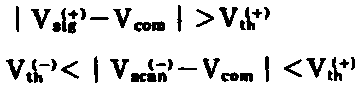
이상이 본 발명을 발명하기에 이른 주요실험 결과이지만, 매트릭스구동을 할 경우를 상정하여 다시 2가지의 실험을 했다. 먼저, 불감대를 약간 넘은 전압![]()
![]()
지금까지의 설명은 광이 액정소자의 됫면으로부터 투과하는 것으로 행했지만, 같은 결과는 뒷면에 반사판을 설치한 이른바 반사형 소자로도 성립된다. 또, 액정중에 색소를 혼입한 이른바 게스트-호스트형 소자에 대해서도 성립된다. 이 경우는 뒷쪽 기판은 투명일 필요는 없다.The explanation so far has been made by the light transmitting from the back surface of the liquid crystal element, but the same result is also achieved by a so-called reflective element in which a reflecting plate is provided on the back side. Moreover, it also holds about what is called a guest-host type element which mixed the pigment | dye in liquid crystal. In this case, the back substrate need not be transparent.
다음에, 강유전성 액정과 액티브매트릭스를 조합한 디스플레이의 실시예에 대하여 제1도에 따라서 설명한다. 박막트랜지스터 등의 3단자 스위치소자(1) 사이에 협지되는 강유전성 액정층(2), 표시전극(21), (22), 신호전극배선(4), 주사전극배선(5) 및 저항 등의 제어소자(3)에 의해 1화소가 구성된다. 이와 같은 화소가 복수의 주사전극과 복수의 신호전극과의 각 교점에 배설되며, 전체로서 액티브매트릭스를 구성한다. 제어소자(3)를 제외한 구성은 종래부터 공지의 액티브매트릭스 디스플레이의 1화소의 구성이다. 3단자스위치소자(1)의 제어단자는 주사전극(5)에, 한쪽의 주단자는 신호전극(4)에, 다른 쪽의 주단자는 표시전극의 한쪽(21)에 접속된다. 제어소자(3)는 3단자스위치소자(1)의 다른 쪽의 주단자와 표시전극의 한쪽(21)과의 접속점과, 전위 Vcont와의 사이에 설치한다. 그리고, 표시전극(22)은 전위 Vcom에 접속된다. 본 발명의 특징은 새로 제어소자(3)를 부가하고, 제어소자(3)를 통해 액정층(2)에 콘트롤신호 Vcont를 인가하여 액정의 광투과상태를 제어하는데 있다. 콘트롤신호 Vcont는 외부에서 주사전압 Vscan이다 신호전압 Vsig과 별개로 인가해도, 또 표시부내의 어느 접점의 전압을 이용하여 인가해도 된다.Next, an embodiment of a display in which a ferroelectric liquid crystal and an active matrix are combined will be described with reference to FIG. Control of ferroelectric
여기서, 제1도의 제어소자(3)의 역할에 대하여 기술한다. 제어소자(3)는 스위치소자(1)가 최소한 오프일때 강유전성 액정(2)에 인가되는 전압의 파고치의 절대치를 강유전성 액정의 한계치( | Vth| )미만으로 유지하기 위한 것이다. 강유전성 액정층(2)은 표시상태가 전압(전계)의존성과 메모리특성을 가지고 있으므로, TN 액정과 같히 스위치소자(1)가 오프의 경우에도 액정층의 전압을 유지할 필요가 없다. 즉, 표시해야 할 화소가 주사전극(5)에 주사전압이 인가되어, 스위치소자(11)가 온일 때에 스위치소자(1)를 통해서, 신호전극(4)으로부터 신호전압이 액정층(2)에 인가된다. 이 인가전압의 절대치가 불감대폭(Vth (-),Vth (+))이상의 전압이면 액정층(2)의 상태가 인가전압에 대응하여 결정된다. 그후, 스위치소자(1)가 온으로 되어 액정층(2)에 한계치( | Vth| ) 미만의 어떠한 전압이 인가되어도, 액정(2)의 상태는 변화하지 않는다. 즉, 제어소자(3)는 스위치소자(1)가 온으로 되어 불감대폭 이상의 신호전압을 기입할 때에는 액정층에 인가되는 전압치를 불감대폭 이상으로, 또 스위치소자(1)가 온이라도, 한계치( | Vth| ) 미만의 신호전압이 액정(2)에 인가될 경우, 및 스위치소자가 오프일 경우 등에는 불감대폭 미만으로 전압을 제어하는 역할도 가지는 것이다.Here, the role of the
다음에, 구체적인 회로의 구성예를 근거로 본 실시예의 내용에 대하여 설명한다. 제2도는 제어소자(3)로서 저항치 R의 저항(5)의 일단을 주사전극배선(5)에 접속한 것이다. 이 때, 스위치소자(1) (이하 스위치소자를 박막트랜지스터: TFT로서 설명함)의 온저항을 Ron, 오프저항을 Roff라고 하면 Ron<R<Roff의 범위내에서 저항(6)의 값 R을 정한다. 제1도의 콘트롤전압 Vcont은 주사전압 Vscan그 자체를 사용한다.Next, the content of this embodiment will be described based on the specific configuration example of the circuit. 2 shows one end of the
제2도의 회로의 인가전압파형의 일실시예를 제3도에 나타낸다. 제3도의 파형은 2계조(二階調)표시의 파형이며, Vscan1, Vscan2,‥ 는 주사전극(5)에 인가되는 주사전압, Vsig1는 선택화소에 인가되는 신호전압, Vsig2는 비선택화소에 인가되는 신호전압, V1c1,은 선택 화소의 액정층에 인가되는 전압, V1c2는 비선택화소의 액정층에 인가되는 전압이다. 여기서, 설명의 편의상 편의적으로 선택화소로서 액정층에 플러스의 전압이 인가되는 화소, 비선택화소로서 마이너스의 잔압이 인가되는 화소로 하고 있다.An example of the voltage waveform applied to the circuit of FIG. 2 is shown in FIG. The waveform in FIG. 3 is a waveform of two gray scale display, V scan1 , V scan2, ... are the scan voltages applied to the
또, 제3도의 신호전압 Vsig1, Vsig2은 각각 선택화소, 비선택화소중에서 가장 인가전압조건이 엄격한 화소의 전압파형을 나타내고 있으며, 이들 조건에 있어서도 표시가 가능하면 어떠한 표시상태에 있어서도 표시가 가능하다. 또, 액정층(2)에 인가되는 전압에 대해서는 선택화소, 비선택화소 저항(6)의 효과를 보기위해 저항(6)이 접속되어 있지 않은 경우의 파형도 동시에 나타내고 있다.In addition, the signal voltages V sig1 and V sig2 in FIG. 3 represent voltage waveforms of pixels having the most severe applied voltage condition among the selected pixel and the non-selected pixel, respectively, and if the display is possible under these conditions, the display is performed in any display state. It is possible. In addition, the voltage applied to the
인가파형의 전압레벨은 다음과 같이 하여 결정한다. 즉, 주사전압 Vscan의 고레벨전압을 Vscan (+), 저레벨전압을 Vscan (-), 신호전압 Vsig의 고레벨전압을 Vsig (+), 저레벨전압을 Vsig (-), 공통전극(대향전극)전압을Vcom, TFT의 온저항을 Ron, 오프저항을 Roff, 저항(6)의 값을 R로 하고, 주사기간내에 액정층(2)이 충분히 충방전 가능하도록 액정층의 용량과 각 저항치가 결정되어 있다고 한다. 또, 간단히 하기 위해 Ron<R<Roff의 관계가 성립되는 것으로 한다. 이 조건은 R/Ron, 또는 Roff/Ron의 값이 10 이상 정도의 값이 기준으로 되므로, 그다지 엄격한 조건은 아니며, 일반 TFT에 있어서는 용이하게 실현할 수 있는 조건이다. 이때, 선택화소에 있어서 TFT소자(1)가 온으로 되는 주사기간에 파고치의 절대치가 한계치(|Vth|) 이상인 제2의 전압신호가 인가되고, TFT소자(1)가 오프로 되는 비주사기간내에 파고치의 절대치가 한계치(|Vth| ) 미만인 제1의 전압신호로 유지하기 위해서는,The voltage level of the applied waveform is determined as follows. That is, the high level voltage of the scan voltage V scan is V scan (+) , the low level voltage is V scan (-) , the high voltage level of the signal voltage V sig is V sig (+) , the low level voltage is V sig (-) , and the common electrode. The counter electrode voltage is V com , the on resistance of the TFT is R on , the off resistance is R off , and the value of the
이다. 한편, 비선택화소에 있어서, TFT소자(1)가 온으로 되는 주사 기간에 있어서, 불감대의 저레벨 Vth에 마이너스의 전압이 인가되고, TFT소자(1)가 오프로 되는 비주사기간내에 불감대내의 전압으로 유지하기 위해서는,to be. On the other hand, in the non-selective pixel, a negative voltage is applied to the low level V th of the dead zone in the scanning period in which the

이다. 이와 같은 전압조건 및 전술한 바와 같은 각 저항간의 값을 취함으로써, 액정에 인가되는 전압은 제3도의 V1c1, V1c2와 같은 파형으로 할 수 있다. 즉, 선택화소에 있어서는 TFT소자가 온이며 화소가 주사되었을 때만, 불감대의 상한 즉 한계치 Vth (+)를 전압이 넘어 액정의 광투과상태가 변화하고, 표시정보가 메모리되며, TFT소자(1)가 오프이며 화소가 주사되지 않을때에는 액정에 인가되는 전압의 파고치의 절대치는 한계치( |Vth| ) 미만으로 유지되므로, 표시정보도 유지된다. 또, 비선택화소에 있어서도 마찬가지로, TFT소자(1)가 온으로 되어 화소가 주사되었을때만, 불감대의 하한 즉 한계치전압 Vth (-)이하의 전압이 인가되어 표시정보가 메모리된다. 한편, 저항(6)을 접속하지 않을 경우는 TFT소자(1)의 오프저항 Roff을 통한 리크전류 때문에 액정소자의 전압이 화소가 선택되지 않은 기간에, 불감대를 넘어버려 광투과 상태가 변화하여 표시정보를 유지할 수 없다는 것을 알 수 있다.to be. By taking the value among the resistance of this voltage and condition described above, the voltage applied to the liquid crystal may be a waveform, such as a third-degree V 1c1, 1c2 V. That is, in the selective pixel, only when the TFT element is on and the pixel is scanned, the light transmission state of the liquid crystal changes beyond the upper limit of the dead band, that is, the threshold value V th (+) , and the display information is stored, and the TFT element 1 ) Is off and the pixel is not scanned, the absolute value of the peak value of the voltage applied to the liquid crystal is kept below the threshold (| V th |), so that the display information is also maintained. Similarly, in the non-selected pixel, only when the
상기 해석은 Ron<Roff의 가정하에서 행했지만, Ron<R<Roff의조건이 성립하도록 저항(6)을 결정하고, 각 저항의 분할에 의한 액정층에의 인가전압을 계산함으로써 구동이 가능하다.The above analysis was performed under the assumption that R on <R off , but the
본 실시예와 같이, 저항(6)을 부가하고, 강유전성 액정과 액티브 매트릭스를 조합하며, 스위치소자에 요구되는 특성이 대폭 완화된다.As in the present embodiment, the
즉, 종래의 액티브매트릭스에서는 액정층에의 기입시간을 결정하는 스위치소자의 온저항 Ron과, 액정층의 전압을 유지하기 위한 스위치 소자의 오프저항 Roff,이 각각의 절대치가 요구되고 있으며, 또 Ron과 Roff와의 비(온·오프비) Roff/Ron도 표시화소수가 wmd가함에 따라 104또는 그 이상의 값이 요구되고 있었다. 이에 대해, 본 발명의 실시예에서는 인가전압을 결정하는 요인은 Ron, Roff와 R와의 관계이며, TFT 등의 스위치소자의 Ron,Roff,에 맞추어서 R을 형성하면 된다. 또한, 액정층의 전압은 이들 저항의 분할비(分割比로 결정하므로 Roff/Ron의 비도 그다지 크게 취할 필요는 없다. 또, 종래 액정층의 전압을 유지하기 위해형성하고 있던 스토리지캐패시터도 형성할 필요는 없다. 이와 같이, 본 발명은 액티브매트릭스 형성에 유효하다.That is, in the conventional active matrix, the absolute values of the on resistance R on of the switch element for determining the writing time to the liquid crystal layer and the off resistance R off of the switch element for maintaining the voltage of the liquid crystal layer are required. Moreover, the ratio (on / off ratio) R off / R on between R on and R off also required 10 4 or more as the display pixel number wmd increased. In contrast, in the embodiment of the present invention, the factor for determining the applied voltage is the relationship between R on and R off and R, and R may be formed in accordance with R on and R off of a switch element such as a TFT. In addition, since the voltage of the liquid crystal layer is determined by the split ratio of these resistors, the ratio of R off / R on does not need to be very large. In addition, the storage capacitors conventionally formed to maintain the voltage of the liquid crystal layer are also formed. In this manner, the present invention is effective for forming an active matrix.
다음에, 제2도의 회로구성을 이용하여 중간조(中間調) 표시를할 경우의 구동파형의 일실시예를 제4도에나타낸다. 강유전성 액정의 특성을 고려하여, 중간조표시를 실현하기 위해서는 다음의 점을 주의하지 않으면 안된다. 예를들면 불감대의 상한 Vth (+)보다 약간 큰 전압펄스 Vp를 인가함으로써, 액정소자의 광투자상태가 중간적인 값으로 안정되며, 중간조의 표시를 얻을 수 있지만, 만약 이 전압펄스 Vp를 계속 인가하면 광투과 상태가 변화해 버리는 현상을 볼 수 있는 것은 이미 기술했다. 즉, 강유전성 액정에서는 전압펄스인가 이전의 인가펄스의 전력(前歷)이 다음의 광투과 상태를 결정하는 현상이 있다. 이 현상을 적극적으로 이용한 구동방법도 생각할 수 있지만, 구동방법이 복잡해진다. 제4도의 실시예는 액정층에 가해지는 전압을 한번 액정소자의 광투과율이 가장 작아지도록 인가하고, 다음에 필요한 중간조의 투과율을 얻는 전압을 인가하는 구동파형이다.Next, FIG. 4 shows an example of the driving waveform in the case of performing halftone display using the circuit configuration of FIG. In view of the characteristics of the ferroelectric liquid crystal, the following points must be taken in order to realize halftone display. For example, by applying a slightly larger voltage pulse V p than the dead band upper limit V th (+), and the light investment of the liquid crystal device is stabilized to an intermediate value, to obtain a halftone display, but if the voltage pulse V p It has already been described that if we continue to apply it, the state of light transmission will change. That is, in ferroelectric liquid crystals, there is a phenomenon in which the power of an applied pulse before application of a voltage pulse determines the next light transmission state. A driving method that actively uses this phenomenon can also be considered, but the driving method becomes complicated. The embodiment of FIG. 4 is a driving waveform in which the voltage applied to the liquid crystal layer is applied so that the light transmittance of the liquid crystal element is the smallest, and then the voltage is applied to obtain the necessary halftone transmittance.
즉, 스위치소자가 온일때 파고치의 절대치가 한계치( |Vth| ) 이상 [바람직하게는 포화치( |Vsat| )이상]인 제2의 전압신호를 인가하여, 액정층의 광투과 상태를 포화상태로 해 두고, 다음에 파고치의 절대치가 한계치( |Vth| ) 이상이며 또한 제2의 전압t신호와는 역극성의 제3의 전압신호를 액정에 인가하여, 중간상태로 하는 방법을 취하고 있다. 이 방법은 액정층의 상태의 전력이 일단 마이너스의 펄스에 의해 클리어되므로 중간상태는 신호전압 Vsig의 크기에 대응하여 얻어진다. 이 구동방법의 상세한 동작을 다음에 기술한다 제1행째의 화소, 제2행째의 화소,‥‥의 주사전극에 인가되는 주사전압을 Vscan1, Vscin2,‥로 하고, 어떤 열의 신호전극에 인가되는 신호전압을 Vsig로 한다. 또, TFT(1)의 온저항 Ron, 저항(6)을 통해 액정층에의 충방전은 신속히 행해지는 것으로 했을 때의 액정층에 인가되는 전압파형은 V1c1,V0c2로 된다.That is, when the switch element is on, a second voltage signal whose absolute value of crest value is greater than or equal to the threshold (| V th |) (preferably greater than or equal to the saturation (| V sat |)) is applied to saturate the light transmission state of the liquid crystal layer. In the state, the absolute value of the crest value is greater than or equal to the limit value (| V th |), and a third voltage signal having a reverse polarity from the second voltage t signal is applied to the liquid crystal to take an intermediate state. have. In this method, since the power of the state of the liquid crystal layer is once cleared by a negative pulse, an intermediate state is obtained corresponding to the magnitude of the signal voltage V sig . The detailed operation of this driving method will be described next. Scanning voltages applied to the scanning electrodes of the pixels of the first row, the pixels of the second row, and the like are applied to the signal electrodes of any column with V scan1 , V scin2,. Let signal voltage be V sig . The voltage waveforms applied to the liquid crystal layer when charging and discharging to the liquid crystal layer through the on-resistance R on and the
먼저, 제1행째가 주사되고 있는 기간 t1,t2중 t1의 기간에서는 주사전압 Vscan1은 TFT소자의 한계치전압보다 낮은 전압이 인가되고 있으므로 TFT소자는 오프상태(TFT는 N채널형으로 되어 있음)이며, 소스ㆍ드레인간은 Roff의 저항으로 되어 있다. 이때, 액정층의 대해 Vscan (-)과 Vsig1과의 전압 및 Roff와 R와의 저항에 의한 전압이 인가되며, 그 크기 V(t1)는First, because the first row is the period of time t 1, the period of t 2 of t 1, which is scanned scanning voltage V scan1 is a low voltage is applied than the threshold voltage of the TFT element TFT element (TFT is an N-channel type OFF state Source and drain are resistors of R off . At this time, the voltage of V scan (−) and V sig1 and the voltage of R off and R are applied to the liquid crystal layer, and the size V (t 1 ) is
![]()
![]()
로 된다. 여기서, Roff가 R에 비해 충분히 크다고 하면 우변 제2항![]()
![]()
![]()
![]()
![]()
![]()
로 되고, R이 Ron에 비해 충분히 큰 것이라고 하면 윗식은![]()
![]()
제5도는 제1도에 있어서 제어전압 Vcont을 인접하는 화소의 주사전극의 전압으로 한 변형예이다. 그 구동파형을 제6도에 나타낸다.5 is a modification in which the control voltage V cont is the voltage of the scan electrodes of adjacent pixels in FIG. The driving waveform is shown in FIG.
주사전압 Vscan1, Vscan2, Vscan3, …은 TFT소자의 주사전압과 다음 라인의 화소의 콘트롤신호 Vcont를 겸용하고 있다. 신호전압 Vsig은 마이너스전위의 기입전압이며, 화소 PE1, PE2‥‥의 액정층에 인가되는 전압을 V1c1, V1c2,‥‥로 한다. 먼저, 화소 PE1의 액정층에 가해지는 전압 V1c1에 주목한다. TFT는 N채널구조라고 하면, 기간 t1의 동안은 화소 PE1의 TFT에는 V1c2가 인가되어 있으므로, 게이트전극전위가 TFT소자의 한계치전압 Vth보다 작아서 TFT소자는 오프상태이며, 채널부는 저항 Roff의 값으로 되어 있다. 그러므로액정층애 인가되는 전압 V1c1(t1)은 Vscan1과 신호전압 Vsig을, 저항 R과 TFT소자의 오프저항 Roff과의 분할로 되며,Scan voltage V scan1 , V scan2 , V scan3,. Combines the scanning voltage of the TFT element and the control signal V cont of the pixel of the next line. The signal voltage V sig is a negative voltage write voltage, and the voltages applied to the liquid crystal layers of the pixels PE1 and PE2 ... are V 1c1 , V 1c2,. First, attention is paid to the voltage V 1c1 applied to the liquid crystal layer of the pixel PE1. If the TFT is an N-channel structure, V 1c2 is applied to the TFT of the pixel PE1 during the period t 1 , so that the gate electrode potential is lower than the threshold voltage V th of the TFT element, and the TFT element is in an off state, and the channel portion is a resistor R. The value is off . Therefore, the voltage V 1c1 (t 1 ) applied to the liquid crystal layer is divided by V scan1 and the signal voltage V sig from the resistance R and the off resistance R off of the TFT element.

로 표현된다. 여기서, Roff> R의 조건에서는 윗 식은![]()
![]()
또, 기간 t2에서는 화소 PE1의 TFT의 게이트전극에 주사전압 Vscan (+)이 인가되어 TFT가 온상태로 되고, 채널부는 Ron의 저항으로 된다. 이때 액정층에 인가되는 전압 Vc1(t2)은In the period t 2 , the scanning voltage V scan (+) is applied to the gate electrode of the TFT of the pixel PE1 to turn the TFT on, and the channel portion becomes the resistance of R on . At this time, the voltage V c1 (t 2 ) applied to the liquid crystal layer is
![]()
![]()
으로 되며, R> Ron의 조건에서는![]()
![]()
![]()
![]()
제7도는 제1도의 실시예에 있어서, 소자(3)를 저항(6)으로 하고, 콘트론신호 Vcont를 공통전극전압Vcom으로 한 구조이다. 이 경우도, 지금까지 기술한 실시예와 대략 같은 효과가 얻어진다.FIG. 7 is a structure in which the
지금까지는 콘트롤신호 Vcont를 화소내의 어떤 전압과 겸용한 구조에 대해 기술했지만, 이것을 제8도와같이 전혀 다른 신호원에 접속해도 된다.Up to now, the structure in which the control signal V cont is combined with a certain voltage in the pixel has been described, but it may be connected to a completely different signal source as shown in FIG.
지금까지의 실시예에서는 액정층의 전압제어용 소자로서 저항을 사용한 예에 대하여 기술했다. 이 소자는 저항 이외에도 각종 소자를 사용할 수 있다.In the above embodiments, an example in which a resistor is used as the voltage control element of the liquid crystal layer has been described. This element can use various elements other than a resistance.
제9도는 TFT소자(7)를 강유전성 액정층(2)의 전압제어용 소자로서 사용한 예이다. 이 실시예에서는TFT소자(1) 및 TFT소자(7)도 N채널형을 사용한 회로구성을 나타낸다.9 shows an example in which the
제10도는 제9도의 회로의 구동방법을 나타낸 것이다. 예를들면 주사전압 Vscan2은 화소 PERoff의 TFT소자(1)의 주사전압과, 화소 PE2의 TFT소자(7)의 주살전압 및 화소 PE2의 액정층의 콘트롤전압 Vcg겸용하고 있다. 기간 t1에 있어서는 Vscan1에 의해 PERoff의 TFT소자(7)가 온상태로 되며, 동시에 Vscan1이 TFT소자(1)를 통해 액정층에 인가된다. 다음에, 기간 t2에 있어서 화소 PE1의 TFT소자(7)는 Vscan1이 저레벨전압으로 되므로 오프상태로 되며, Vscan2에 의해 TFT소자(1)가 온상태로 된다. 이로써, 신호전압 Vsig이 TFT소자(1)를 통해 액정층에 인가된다. 여기써, 주사전압 Vscan1, Vscan2, …을 액정층의 한계치전압의 절대치( |Vth| ) 보다 충분히 큰 전압으로 설정함으로써, 액정층에 신호전압이 인가되기 전에 한번 플러스의 값의 전압이 인가되어 액정층의 상태가 리세트된다 여기서, 신호전압 Vsig의 전압레벨을 조정함으로써, 중간조표시나 2계조표시의 모두가 가능하다.FIG. 10 shows a method of driving the circuit of FIG. For example, the scan voltage V scan2 combines the scan voltage of the
TFT소자의 오프저항 Roff이 충분히 클 경우에는 신호전극(4)에서 신호전압 Vsig의 리크가 없고, 액정층에 불필요한 전압이 인가되지 않으므로 특히 문제는 생기지 않는다. 그러나, TFT소자의 오프저항 Roff이 충분하지 않을 경우는 신호전압의 리크를 작게 억제하기 위해, TFT소자(1)외 오프저항 Roff과 TFT소자(7)의 오프저항 Roff7과의 사이에 Roff1>Roff7로 되도록 TFT소자를 설계하지 않으면 안된다. 이를 위해서는, TFT소자형상, 즉 채널길이 L와 채널폭 W을 조정하고, 오프저항 Roff을 변화시킬 필요가 있다. 또는, 어느 1개의 TFT소자의 채널부에 이온주입 등의 방법에 의해 불순물을 도핑하고, TFT소자의 한계치전압Vth을 변화시켜서, 동작점에서의 오프저항 Roff을 변화시키는 방법 등을 들 수 있다.If the off-resistance R off of the TFT element is sufficiently large, there is no leak of the signal voltage V sig in the
제11도는 TFT소자(1)의 주사전극에 콘트롤신호를 접속하고 TFT소자(7)의 주사전압은 이 화소의 1행앞(필요에 따라서는 복수행 앞)의 주사전극에 접속한 구조이다. 구동방법은 제12도와 같이 예를들면 Vscan2는 화소 PE1의 액정층을 마이너스의 전압에 의해 리세트하는 역할과 다음의 기간에 TFT소자(1)를 주사하여 온상태로 하는 역할을 갖고 있다.11 shows a structure in which a control signal is connected to the scanning electrode of the
지금까지의 실시예에서는 1화소내에 형성하는 2개의 TPF소자는 모두 N채널구조로 하였으나, 이것을 P채널 구조의 TFT와 N채널구조의 TFT를 조합한 구성이라도 된다. 제13도는 양 채널의 소자를 조압했을때의 회로의 실시예이다. TFT소자(1)를 N채널, TFT소자(7)를 P채널의 구성으로 해도, 또 그 역의 조합으로 해도 동작가능하다. 제14도는 TFT소자(1)를 N채널, TFT소자(T)를 P채널로 한 경우의 구동파형, 또 제15도는 TFT소자(1)를 P채널, TFT소자(7)를 N채널로 한 경우의 구동파형을 나타낸다.In the above embodiments, the two TPF elements formed in one pixel have an N-channel structure, but this may be a combination of a TFT having a P-channel structure and a TFT having an N-channel structure. FIG. 13 shows an example of a circuit when the elements of both channels are regulated. It is possible to operate the
제16도에 강유전성 액정을 사용한 액티브내트릭스 디스플레이의 부분단면 개략구조를 나타낸다. 기판(8)은 예를들면 바륨붕규산유리나 석영유리 등의 투명기판이며, 그 위에 다결정실리콘막이나 재결정화실리콘막등의 반도체박막(12), 절연막(13)을 형성하고, 공지의 제조프로세스로 게이트전극(15), 드레인전극(14), 투명전극(10) 등을 형성하여, TFT소자를 제작했다. 그후, TFT상에 예를들면 유기물의 박막인 유기도포막(16)을 스피너도포 등에 의해 형성하고, TFT부 이외의 부분을 제거하였다. 그 위에 유리기판을 적층하였다. 이와 같은 구조로 함으로써, 셀갭(cell gap)은 TFT의 높이와 유기도포막(16)에 의해 결정되며, 2㎛정도 또는 그 이외의 갭을 표시부 전역에 걸쳐서 형성할 수 있다. 여기서, 앞에 기술한 성분의 액정을 봉입하고 강유전성 액정과 액티브매트릭스를 적층한 디스플레이를 형성할 수 있다.Fig. 16 shows a partial cross-sectional schematic structure of an active matrix display using ferroelectric liquid crystals. The
본 발명에 의하면, 강유전성 액정의 특성을 이용하여 특성이 불충분한 TFT소자 등의 스위치소자를 사용해도 양호한 구동이 가능해진다.According to the present invention, even if a switch element such as a TFT element having insufficient characteristics by using the characteristics of the ferroelectric liquid crystal is used, good driving can be achieved.
또한, TFT소자 등의 스위치소자의 제어전극에 인가하는 주사전압을 이용하여. 액정층을 미리 포화상태로 해 두고, 그후 신호전압에 의해 중간상태를 실현하므로, 재현성이 양호한 중간조표시를 얻을 수 있다.Further, by using a scanning voltage applied to the control electrode of the switch element such as the TFT element. Since the liquid crystal layer is made saturated in advance and then the intermediate state is realized by the signal voltage, halftone display with good reproducibility can be obtained.
Claims (14)
Applications Claiming Priority (3)
| Application Number | Priority Date | Filing Date | Title |
|---|---|---|---|
| JP184,646 | 1984-09-05 | ||
| JP84-184646 | 1984-09-05 | ||
| JP59184646A JPH0693166B2 (en) | 1984-09-05 | 1984-09-05 | Liquid crystal element |
Publications (2)
| Publication Number | Publication Date |
|---|---|
| KR860002730A KR860002730A (en) | 1986-04-28 |
| KR930010456B1 true KR930010456B1 (en) | 1993-10-25 |
Family
ID=16156872
Family Applications (1)
| Application Number | Title | Priority Date | Filing Date |
|---|---|---|---|
| KR1019850006186A KR930010456B1 (en) | 1984-09-05 | 1985-08-27 | Liquid crystal device and method of driving the same |
Country Status (5)
| Country | Link |
|---|---|
| US (1) | US4818077A (en) |
| EP (1) | EP0176763B1 (en) |
| JP (1) | JPH0693166B2 (en) |
| KR (1) | KR930010456B1 (en) |
| DE (1) | DE3574515D1 (en) |
Families Citing this family (70)
| Publication number | Priority date | Publication date | Assignee | Title |
|---|---|---|---|---|
| FR2593632B1 (en) * | 1986-01-27 | 1988-03-18 | Maurice Francois | ACTIVE MATRIX DISPLAY SCREEN AND METHODS OF MAKING SAME |
| US7864151B1 (en) | 1986-07-07 | 2011-01-04 | Semiconductor Energy Laboratory Co., Ltd. | Portable electronic device |
| FR2605442B1 (en) * | 1986-10-17 | 1988-12-09 | Thomson Csf | ELECTROOPTIC VISUALIZATION SCREEN WITH CONTROL TRANSISTORS AND METHOD FOR PRODUCING THE SAME |
| FR2606194B1 (en) * | 1986-11-05 | 1989-02-17 | Commissariat Energie Atomique | MATRIX DISPLAY DEVICE AND CONTROL METHOD THEREOF |
| NL8700627A (en) * | 1987-03-17 | 1988-10-17 | Philips Nv | METHOD FOR CONTROLLING A LIQUID CRYSTAL DISPLAY AND ASSOCIATED DISPLAY. |
| KR920007167B1 (en) * | 1987-04-20 | 1992-08-27 | 가부시기가이샤 히다씨세이사구쇼 | Liquid crystal display apparatus and the method of driving the same |
| NL8701420A (en) * | 1987-06-18 | 1989-01-16 | Philips Nv | DISPLAY DEVICE AND METHOD FOR CONTROLLING SUCH DISPLAY DEVICE. |
| EP0296663B1 (en) * | 1987-06-18 | 1994-03-30 | Koninklijke Philips Electronics N.V. | Display device |
| NL8703040A (en) * | 1987-12-16 | 1989-07-17 | Philips Nv | METHOD FOR CONTROLLING A PASSIVE FERRO-ELECTRIC LIQUID CRYSTAL DISPLAY. |
| JPH01161316A (en) * | 1987-12-18 | 1989-06-26 | Sharp Corp | Liquid crystal display device |
| NL8703085A (en) * | 1987-12-21 | 1989-07-17 | Philips Nv | METHOD FOR CONTROLLING A DISPLAY DEVICE |
| NL8802155A (en) * | 1988-09-01 | 1990-04-02 | Philips Nv | DISPLAY DEVICE. |
| FR2637408A1 (en) * | 1988-09-30 | 1990-04-06 | Commissariat Energie Atomique | METHOD OF ADDRESSING A FERROELECTRIC LIQUID CRYSTAL DISPLAY SCREEN WITH CHIRAL SMECTIC PHASE |
| GB2223618A (en) * | 1988-10-07 | 1990-04-11 | Philips Electronic Associated | Display devices |
| US5051570A (en) * | 1989-01-20 | 1991-09-24 | Nec Corporation | Liquid crystal light valve showing an improved display contrast |
| US5227900A (en) * | 1990-03-20 | 1993-07-13 | Canon Kabushiki Kaisha | Method of driving ferroelectric liquid crystal element |
| US6893906B2 (en) * | 1990-11-26 | 2005-05-17 | Semiconductor Energy Laboratory Co., Ltd. | Electro-optical device and driving method for the same |
| US5849601A (en) | 1990-12-25 | 1998-12-15 | Semiconductor Energy Laboratory Co., Ltd. | Electro-optical device and method for manufacturing the same |
| KR950013784B1 (en) | 1990-11-20 | 1995-11-16 | 가부시키가이샤 한도오따이 에네루기 겐큐쇼 | Field effect trasistor and its making method and tft |
| US5514879A (en) * | 1990-11-20 | 1996-05-07 | Semiconductor Energy Laboratory Co., Ltd. | Gate insulated field effect transistors and method of manufacturing the same |
| US7115902B1 (en) | 1990-11-20 | 2006-10-03 | Semiconductor Energy Laboratory Co., Ltd. | Electro-optical device and method for manufacturing the same |
| KR950001360B1 (en) * | 1990-11-26 | 1995-02-17 | 가부시키가이샤 한도오따이 에네루기 겐큐쇼 | Electric optical device and driving method thereof |
| US8106867B2 (en) | 1990-11-26 | 2012-01-31 | Semiconductor Energy Laboratory Co., Ltd. | Electro-optical device and driving method for the same |
| TW209895B (en) * | 1990-11-26 | 1993-07-21 | Semiconductor Energy Res Co Ltd | |
| US7154147B1 (en) | 1990-11-26 | 2006-12-26 | Semiconductor Energy Laboratory Co., Ltd. | Electro-optical device and driving method for the same |
| JP2999271B2 (en) * | 1990-12-10 | 2000-01-17 | 株式会社半導体エネルギー研究所 | Display device |
| KR960010723B1 (en) * | 1990-12-20 | 1996-08-07 | 가부시끼가이샤 한도오따이 에네루기 겐큐쇼 | Liquid crystal electro-optical device |
| US7576360B2 (en) * | 1990-12-25 | 2009-08-18 | Semiconductor Energy Laboratory Co., Ltd. | Electro-optical device which comprises thin film transistors and method for manufacturing the same |
| US7098479B1 (en) | 1990-12-25 | 2006-08-29 | Semiconductor Energy Laboratory Co., Ltd. | Electro-optical device and method for manufacturing the same |
| US5854494A (en) * | 1991-02-16 | 1998-12-29 | Semiconductor Energy Laboratory Co., Ltd. | Electric device, matrix device, electro-optical display device, and semiconductor memory having thin-film transistors |
| EP0499979A3 (en) * | 1991-02-16 | 1993-06-09 | Semiconductor Energy Laboratory Co., Ltd. | Electro-optical device |
| US6028333A (en) * | 1991-02-16 | 2000-02-22 | Semiconductor Energy Laboratory Co., Ltd. | Electric device, matrix device, electro-optical display device, and semiconductor memory having thin-film transistors |
| JP3556679B2 (en) * | 1992-05-29 | 2004-08-18 | 株式会社半導体エネルギー研究所 | Electro-optical device |
| US6713783B1 (en) | 1991-03-15 | 2004-03-30 | Semiconductor Energy Laboratory Co., Ltd. | Compensating electro-optical device including thin film transistors |
| JP2873632B2 (en) * | 1991-03-15 | 1999-03-24 | 株式会社半導体エネルギー研究所 | Semiconductor device |
| JP2794499B2 (en) * | 1991-03-26 | 1998-09-03 | 株式会社半導体エネルギー研究所 | Method for manufacturing semiconductor device |
| US5680147A (en) * | 1991-05-20 | 1997-10-21 | Semiconductor Energy Laboratory Co., Ltd. | Electro-optical device and method of driving the same |
| JP2838338B2 (en) * | 1991-05-21 | 1998-12-16 | 株式会社半導体エネルギー研究所 | Driving method of electro-optical device |
| US6778231B1 (en) | 1991-06-14 | 2004-08-17 | Semiconductor Energy Laboratory Co., Ltd. | Electro-optical display device |
| US5414442A (en) * | 1991-06-14 | 1995-05-09 | Semiconductor Energy Laboratory Co., Ltd. | Electro-optical device and method of driving the same |
| US6975296B1 (en) | 1991-06-14 | 2005-12-13 | Semiconductor Energy Laboratory Co., Ltd. | Electro-optical device and method of driving the same |
| JP2746486B2 (en) * | 1991-08-20 | 1998-05-06 | シャープ株式会社 | Ferroelectric liquid crystal device |
| JP2845303B2 (en) * | 1991-08-23 | 1999-01-13 | 株式会社 半導体エネルギー研究所 | Semiconductor device and manufacturing method thereof |
| EP0541364B1 (en) * | 1991-11-07 | 1998-04-01 | Canon Kabushiki Kaisha | Liquid crystal device and driving method therefor |
| JPH05134626A (en) * | 1991-11-11 | 1993-05-28 | Sharp Corp | Liquid crystal element and driving method therefor |
| JP2651972B2 (en) * | 1992-03-04 | 1997-09-10 | 株式会社半導体エネルギー研究所 | Liquid crystal electro-optical device |
| JPH06289367A (en) * | 1992-03-04 | 1994-10-18 | Shunsuke Kobayashi | Liquid crystal display device |
| GB2265486A (en) * | 1992-03-11 | 1993-09-29 | Marconi Gec Ltd | Display device fabrication |
| US6693681B1 (en) | 1992-04-28 | 2004-02-17 | Semiconductor Energy Laboratory Co., Ltd. | Electro-optical device and method of driving the same |
| JP2814161B2 (en) | 1992-04-28 | 1998-10-22 | 株式会社半導体エネルギー研究所 | Active matrix display device and driving method thereof |
| JP3173200B2 (en) * | 1992-12-25 | 2001-06-04 | ソニー株式会社 | Active matrix type liquid crystal display |
| US7081938B1 (en) * | 1993-12-03 | 2006-07-25 | Semiconductor Energy Laboratory Co., Ltd. | Electro-optical device and method for manufacturing the same |
| US6747627B1 (en) | 1994-04-22 | 2004-06-08 | Semiconductor Energy Laboratory Co., Ltd. | Redundancy shift register circuit for driver circuit in active matrix type liquid crystal display device |
| JP3402400B2 (en) * | 1994-04-22 | 2003-05-06 | 株式会社半導体エネルギー研究所 | Manufacturing method of semiconductor integrated circuit |
| JPH07302912A (en) * | 1994-04-29 | 1995-11-14 | Semiconductor Energy Lab Co Ltd | Semiconductor device |
| JP2900229B2 (en) * | 1994-12-27 | 1999-06-02 | 株式会社半導体エネルギー研究所 | Semiconductor device, manufacturing method thereof, and electro-optical device |
| US5834327A (en) | 1995-03-18 | 1998-11-10 | Semiconductor Energy Laboratory Co., Ltd. | Method for producing display device |
| TW439003B (en) * | 1995-11-17 | 2001-06-07 | Semiconductor Energy Lab | Display device |
| US6800875B1 (en) * | 1995-11-17 | 2004-10-05 | Semiconductor Energy Laboratory Co., Ltd. | Active matrix electro-luminescent display device with an organic leveling layer |
| TW309633B (en) | 1995-12-14 | 1997-07-01 | Handotai Energy Kenkyusho Kk | |
| US6225218B1 (en) | 1995-12-20 | 2001-05-01 | Semiconductor Energy Laboratory Co., Ltd. | Semiconductor device and its manufacturing method |
| JP3725266B2 (en) * | 1996-11-07 | 2005-12-07 | 株式会社半導体エネルギー研究所 | Wiring formation method |
| US5937906A (en) * | 1997-05-06 | 1999-08-17 | Kozyuk; Oleg V. | Method and apparatus for conducting sonochemical reactions and processes using hydrodynamic cavitation |
| DE19832995C1 (en) * | 1998-07-22 | 1999-11-04 | Siemens Ag | Memory device using resistive ferroelectric memory cells |
| US6475836B1 (en) * | 1999-03-29 | 2002-11-05 | Semiconductor Energy Laboratory Co., Ltd. | Semiconductor device and manufacturing method thereof |
| DE60035075T2 (en) * | 1999-11-12 | 2008-01-24 | Sony Corp. | A light modulation device, image pickup device and method of its exposure time control |
| TWI246197B (en) * | 2001-09-27 | 2005-12-21 | Prime View Int Corp Ltd | TFT LCD structure containing conductive balls and the manufacturing method thereof |
| WO2005038767A1 (en) * | 2003-10-17 | 2005-04-28 | Scanvue Technologies Llc | Shared select line display |
| JP2012093435A (en) * | 2010-10-25 | 2012-05-17 | Chi Mei Electronics Corp | Display device and electronic apparatus including the same |
| KR20120049022A (en) * | 2010-11-08 | 2012-05-16 | 삼성모바일디스플레이주식회사 | Liquid crystal display device and driving method of the same |
Family Cites Families (15)
| Publication number | Priority date | Publication date | Assignee | Title |
|---|---|---|---|---|
| US3654606A (en) * | 1969-11-06 | 1972-04-04 | Rca Corp | Alternating voltage excitation of liquid crystal display matrix |
| US3873888A (en) * | 1974-03-27 | 1975-03-25 | Rca Corp | Liquid crystal protection circuit |
| JPS5757716B2 (en) * | 1974-05-16 | 1982-12-06 | Citizen Watch Co Ltd | |
| JPS5144896A (en) * | 1974-10-16 | 1976-04-16 | Hitachi Ltd | EKISHOHYOJISOCHI |
| US4062626A (en) * | 1974-09-20 | 1977-12-13 | Hitachi, Ltd. | Liquid crystal display device |
| DE2523763A1 (en) * | 1975-05-28 | 1976-12-09 | Siemens Ag | Liquid crystal display device - has matrix of row and column conducting traces on circuit boards between which liquid crystal is held |
| US4245168A (en) * | 1978-08-03 | 1981-01-13 | General Electric Company | Integratable driver for liquid crystal displays and the like |
| US4448491A (en) * | 1979-08-08 | 1984-05-15 | Canon Kabushiki Kaisha | Image display apparatus |
| US4367924A (en) * | 1980-01-08 | 1983-01-11 | Clark Noel A | Chiral smectic C or H liquid crystal electro-optical device |
| US4529271A (en) * | 1982-03-12 | 1985-07-16 | At&T Bell Laboratories | Matrix addressed bistable liquid crystal display |
| JPH0629919B2 (en) * | 1982-04-16 | 1994-04-20 | 株式会社日立製作所 | Liquid crystal element driving method |
| JPS5934587A (en) * | 1982-08-23 | 1984-02-24 | 株式会社日立製作所 | Liquid crystal device |
| JPS59129837A (en) * | 1983-01-14 | 1984-07-26 | Canon Inc | Applying method of time division voltage |
| US4655561A (en) * | 1983-04-19 | 1987-04-07 | Canon Kabushiki Kaisha | Method of driving optical modulation device using ferroelectric liquid crystal |
| JPS6152630A (en) * | 1984-08-22 | 1986-03-15 | Hitachi Ltd | Driving method of liquid crystal element |
-
1984
- 1984-09-05 JP JP59184646A patent/JPH0693166B2/en not_active Expired - Lifetime
-
1985
- 1985-08-27 KR KR1019850006186A patent/KR930010456B1/en not_active IP Right Cessation
- 1985-08-28 DE DE8585110812T patent/DE3574515D1/en not_active Expired - Lifetime
- 1985-08-28 US US06/770,204 patent/US4818077A/en not_active Expired - Fee Related
- 1985-08-28 EP EP85110812A patent/EP0176763B1/en not_active Expired
Also Published As
| Publication number | Publication date |
|---|---|
| US4818077A (en) | 1989-04-04 |
| JPH0693166B2 (en) | 1994-11-16 |
| EP0176763A1 (en) | 1986-04-09 |
| JPS6163895A (en) | 1986-04-02 |
| KR860002730A (en) | 1986-04-28 |
| DE3574515D1 (en) | 1990-01-04 |
| EP0176763B1 (en) | 1989-11-29 |
Similar Documents
| Publication | Publication Date | Title |
|---|---|---|
| KR930010456B1 (en) | Liquid crystal device and method of driving the same | |
| US5691783A (en) | Liquid crystal display device and method for driving the same | |
| US4697887A (en) | Liquid crystal device and method for driving the same using ferroelectric liquid crystal and FET's | |
| KR100300280B1 (en) | Active matrix light modulators and display | |
| EP0554109B1 (en) | Method for driving a liquid crystal display | |
| JPS6261931B2 (en) | ||
| KR0138968B1 (en) | Electro-optical device | |
| JP3551702B2 (en) | Liquid crystal display device and driving method thereof | |
| US5598284A (en) | Electro-optical device defined by relationship of data voltage, residual voltage, spontaneous polarization, and liquid crystal time constant and capacitance | |
| KR100473874B1 (en) | Liquid crystal device | |
| US20050001972A1 (en) | Bistable liquid crystal device having two drive modes | |
| US6473117B1 (en) | Driving method for liquid crystal device | |
| US7348953B1 (en) | Method of driving liquid crystal display device | |
| JP2984789B2 (en) | Display element device and display element driving method | |
| US6069602A (en) | Liquid crystal display device, liquid crystal display apparatus and liquid crystal driving method | |
| JP3262870B2 (en) | Liquid crystal electro-optical device | |
| US20010045933A1 (en) | Liquid crystal optical apparatus | |
| JPH0414766B2 (en) | ||
| JP3259634B2 (en) | Antiferroelectric liquid crystal display | |
| JP2000019485A (en) | Method for driving liquid crystal device | |
| JPH06194625A (en) | Driving method for ferroelectric liquid crystal display element | |
| JPH1082985A (en) | Display element and display element device | |
| JPH08328046A (en) | Antiferroelectric liquid crystal display element | |
| JP4678935B2 (en) | Driving method of liquid crystal display device | |
| JPH0968728A (en) | Liquid crystal display element formed by using liquid crystal having spontaneous polarization |
Legal Events
| Date | Code | Title | Description |
|---|---|---|---|
| A201 | Request for examination | ||
| E902 | Notification of reason for refusal | ||
| G160 | Decision to publish patent application | ||
| E701 | Decision to grant or registration of patent right | ||
| GRNT | Written decision to grant | ||
| FPAY | Annual fee payment |
Payment date: 19991006 Year of fee payment: 7 |
|
| LAPS | Lapse due to unpaid annual fee |