KR930006301B1 - Method for forming thin-film and device therefor - Google Patents
Method for forming thin-film and device therefor Download PDFInfo
- Publication number
- KR930006301B1 KR930006301B1 KR1019900009730A KR900009730A KR930006301B1 KR 930006301 B1 KR930006301 B1 KR 930006301B1 KR 1019900009730 A KR1019900009730 A KR 1019900009730A KR 900009730 A KR900009730 A KR 900009730A KR 930006301 B1 KR930006301 B1 KR 930006301B1
- Authority
- KR
- South Korea
- Prior art keywords
- gas
- substrate
- thin film
- separated
- types
- Prior art date
Links
Images


Classifications
-
- H—ELECTRICITY
- H01—ELECTRIC ELEMENTS
- H01L—SEMICONDUCTOR DEVICES NOT COVERED BY CLASS H10
- H01L21/00—Processes or apparatus adapted for the manufacture or treatment of semiconductor or solid state devices or of parts thereof
- H01L21/02—Manufacture or treatment of semiconductor devices or of parts thereof
- H01L21/04—Manufacture or treatment of semiconductor devices or of parts thereof the devices having at least one potential-jump barrier or surface barrier, e.g. PN junction, depletion layer or carrier concentration layer
- H01L21/18—Manufacture or treatment of semiconductor devices or of parts thereof the devices having at least one potential-jump barrier or surface barrier, e.g. PN junction, depletion layer or carrier concentration layer the devices having semiconductor bodies comprising elements of Group IV of the Periodic System or AIIIBV compounds with or without impurities, e.g. doping materials
- H01L21/20—Deposition of semiconductor materials on a substrate, e.g. epitaxial growth solid phase epitaxy
- H01L21/205—Deposition of semiconductor materials on a substrate, e.g. epitaxial growth solid phase epitaxy using reduction or decomposition of a gaseous compound yielding a solid condensate, i.e. chemical deposition
-
- H—ELECTRICITY
- H01—ELECTRIC ELEMENTS
- H01J—ELECTRIC DISCHARGE TUBES OR DISCHARGE LAMPS
- H01J37/00—Discharge tubes with provision for introducing objects or material to be exposed to the discharge, e.g. for the purpose of examination or processing thereof
- H01J37/32—Gas-filled discharge tubes
- H01J37/32009—Arrangements for generation of plasma specially adapted for examination or treatment of objects, e.g. plasma sources
- H01J37/32422—Arrangement for selecting ions or species in the plasma
-
- C—CHEMISTRY; METALLURGY
- C23—COATING METALLIC MATERIAL; COATING MATERIAL WITH METALLIC MATERIAL; CHEMICAL SURFACE TREATMENT; DIFFUSION TREATMENT OF METALLIC MATERIAL; COATING BY VACUUM EVAPORATION, BY SPUTTERING, BY ION IMPLANTATION OR BY CHEMICAL VAPOUR DEPOSITION, IN GENERAL; INHIBITING CORROSION OF METALLIC MATERIAL OR INCRUSTATION IN GENERAL
- C23C—COATING METALLIC MATERIAL; COATING MATERIAL WITH METALLIC MATERIAL; SURFACE TREATMENT OF METALLIC MATERIAL BY DIFFUSION INTO THE SURFACE, BY CHEMICAL CONVERSION OR SUBSTITUTION; COATING BY VACUUM EVAPORATION, BY SPUTTERING, BY ION IMPLANTATION OR BY CHEMICAL VAPOUR DEPOSITION, IN GENERAL
- C23C14/00—Coating by vacuum evaporation, by sputtering or by ion implantation of the coating forming material
- C23C14/22—Coating by vacuum evaporation, by sputtering or by ion implantation of the coating forming material characterised by the process of coating
- C23C14/221—Ion beam deposition
-
- C—CHEMISTRY; METALLURGY
- C23—COATING METALLIC MATERIAL; COATING MATERIAL WITH METALLIC MATERIAL; CHEMICAL SURFACE TREATMENT; DIFFUSION TREATMENT OF METALLIC MATERIAL; COATING BY VACUUM EVAPORATION, BY SPUTTERING, BY ION IMPLANTATION OR BY CHEMICAL VAPOUR DEPOSITION, IN GENERAL; INHIBITING CORROSION OF METALLIC MATERIAL OR INCRUSTATION IN GENERAL
- C23C—COATING METALLIC MATERIAL; COATING MATERIAL WITH METALLIC MATERIAL; SURFACE TREATMENT OF METALLIC MATERIAL BY DIFFUSION INTO THE SURFACE, BY CHEMICAL CONVERSION OR SUBSTITUTION; COATING BY VACUUM EVAPORATION, BY SPUTTERING, BY ION IMPLANTATION OR BY CHEMICAL VAPOUR DEPOSITION, IN GENERAL
- C23C16/00—Chemical coating by decomposition of gaseous compounds, without leaving reaction products of surface material in the coating, i.e. chemical vapour deposition [CVD] processes
- C23C16/44—Chemical coating by decomposition of gaseous compounds, without leaving reaction products of surface material in the coating, i.e. chemical vapour deposition [CVD] processes characterised by the method of coating
- C23C16/448—Chemical coating by decomposition of gaseous compounds, without leaving reaction products of surface material in the coating, i.e. chemical vapour deposition [CVD] processes characterised by the method of coating characterised by the method used for generating reactive gas streams, e.g. by evaporation or sublimation of precursor materials
- C23C16/452—Chemical coating by decomposition of gaseous compounds, without leaving reaction products of surface material in the coating, i.e. chemical vapour deposition [CVD] processes characterised by the method of coating characterised by the method used for generating reactive gas streams, e.g. by evaporation or sublimation of precursor materials by activating reactive gas streams before their introduction into the reaction chamber, e.g. by ionisation or addition of reactive species
-
- C—CHEMISTRY; METALLURGY
- C23—COATING METALLIC MATERIAL; COATING MATERIAL WITH METALLIC MATERIAL; CHEMICAL SURFACE TREATMENT; DIFFUSION TREATMENT OF METALLIC MATERIAL; COATING BY VACUUM EVAPORATION, BY SPUTTERING, BY ION IMPLANTATION OR BY CHEMICAL VAPOUR DEPOSITION, IN GENERAL; INHIBITING CORROSION OF METALLIC MATERIAL OR INCRUSTATION IN GENERAL
- C23C—COATING METALLIC MATERIAL; COATING MATERIAL WITH METALLIC MATERIAL; SURFACE TREATMENT OF METALLIC MATERIAL BY DIFFUSION INTO THE SURFACE, BY CHEMICAL CONVERSION OR SUBSTITUTION; COATING BY VACUUM EVAPORATION, BY SPUTTERING, BY ION IMPLANTATION OR BY CHEMICAL VAPOUR DEPOSITION, IN GENERAL
- C23C16/00—Chemical coating by decomposition of gaseous compounds, without leaving reaction products of surface material in the coating, i.e. chemical vapour deposition [CVD] processes
- C23C16/44—Chemical coating by decomposition of gaseous compounds, without leaving reaction products of surface material in the coating, i.e. chemical vapour deposition [CVD] processes characterised by the method of coating
- C23C16/50—Chemical coating by decomposition of gaseous compounds, without leaving reaction products of surface material in the coating, i.e. chemical vapour deposition [CVD] processes characterised by the method of coating using electric discharges
-
- H—ELECTRICITY
- H01—ELECTRIC ELEMENTS
- H01J—ELECTRIC DISCHARGE TUBES OR DISCHARGE LAMPS
- H01J37/00—Discharge tubes with provision for introducing objects or material to be exposed to the discharge, e.g. for the purpose of examination or processing thereof
- H01J37/32—Gas-filled discharge tubes
- H01J37/32009—Arrangements for generation of plasma specially adapted for examination or treatment of objects, e.g. plasma sources
- H01J37/32357—Generation remote from the workpiece, e.g. down-stream
Abstract
내용 없음.No content.
Description
제1도는 본 발명에 따른 제1실시예의 박막형성장치를 도시한 개략구성도.1 is a schematic configuration diagram showing a thin film forming apparatus of a first embodiment according to the present invention.
제2도는 본 발명의 제3실시예를 도시한 개략구성도.2 is a schematic configuration diagram showing a third embodiment of the present invention.
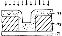
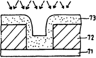
제3a 내지 b도는 단차피복성을 도시한 단면도.3A to 3B are cross-sectional views showing step coverage.
제4도는 적외선흡수스펙트럼을 도시한 특성도.4 is a characteristic diagram showing an infrared absorption spectrum.
제5도는 본 발명에 따른 제6실시예의 박막형성장치를 도시한 개략구성도.5 is a schematic diagram showing a thin film forming apparatus of a sixth embodiment according to the present invention;
제6도는 본 발명에 따른 제7실시예의 박막형성장치의 일부를 도시한 요부구성도.6 is a main structural view showing part of a thin film forming apparatus of a seventh embodiment according to the present invention;
제7a 및 b도는 시료에 이온이 조사된 상태를 도시하는 설명도.7A and 7B are explanatory diagrams showing a state in which ions are irradiated to a sample.
제8a 내지 c도는 오버행부(overhang部)에 박막을 형성하는 경우를 설명하기 위한 단면도이다.8A to 8C are cross-sectional views for explaining the case where a thin film is formed in an overhang portion.
* 도면의 주요부분에 대한 부호의 설명* Explanation of symbols for main parts of the drawings
10 : 반응로 11 : 기판10 reactor 11: substrate
12 : 시료대 13 : 히터12: sample stand 13: heater
14a,14b : 디플렉터 16 : 모터14a, 14b: deflector 16: motor
20 : 가스종류분리공급챔버 21a,21b : 이온원(ion源)20: gas type
22a,22b : 인출전극 23a,23b,24a,24b : 집속렌즈22a, 22b:
25a,25b : 질량필터 26a,26b :감속기25a, 25b:
27a,27b : 중성화실 30 : 반응로27a, 27b: neutralization chamber 30: reactor
31 : 기판 32 : 시료대31
33 : 히터 34 : 전극33
35 : 고주파전원 36 : 배기로35: high frequency power supply 36: exhaust passage
41 : 제1석영관 42 : 칠러(chiller)41: 1st quartz building 42: chiller
43 : 제2석영관 44 : 가스도입관43: second quartz tube 44: gas introduction tube
45 : 도파기 46 : 고주파전원45: waveguide 46: high frequency power supply
47 : 히터 51 : 가스도입관47: heater 51: gas introduction pipe
52 : 도파기 53 : 고주파전원52: waveguide 53: high frequency power supply
54 : 절연체 55,56,57 : 가스켓54:
60 : 반응용기 61 : 반응관60: reaction vessel 61: reaction tube
62 : 석영보드 63 : 실리콘웨이퍼62: quartz board 63: silicon wafer
64 : 전극 65 : 고주파전원64
66 : 히터 71 : 기판66: heater 71: substrate
72 : 하지막(下地膜) 73 : 형성박막72: underlayer 73: forming thin film
81 : 기판 83 : 박막81: substrate 83: thin film
[산업상의 이용분야][Industrial use]
본 발명은 초 LSI등의 반도체디바이스의 제조에 적용되는 박막형성기술에 관한 것으로, 특히, 화학기상성장법(CVD法)용한 박막형성방법 및 박막형성장치에 관한 것이다.BACKGROUND OF THE INVENTION 1. Field of the Invention The present invention relates to a thin film forming technology applied to the manufacture of semiconductor devices such as ultra LSI, and more particularly, to a thin film forming method and a thin film forming apparatus using chemical vapor deposition (CVD).
[종래의 기술 및 그 문제점][Traditional Technology and Problems]
근년, 반도체디바이스의 제조공정에 있어서 CVD법이 널리 이용되고 있다. CVD법은 기판이 수용되는 반응로내에 소정의 가스를 공급하고, 기판표면에서 가스를 화학반응시켜, 기판상에 박막을 퇴적하는 방법이다. 이중 플라즈마 CVD법이나 광 CV D법은 플라즈마나 광에 의해 가스의 활성화효율을 높이므로, 저온에서도 고속으로 퇴적시킬 수 있다. 이 때문에 플라즈마 CVD법이나 광 CVD법은 반도체디바이스의 제조에 있어서 매우 유효하다. 따라서, 플라즈마 CVD법이나 광 CVD법은 반도체디바이스의 제조공정의 저온화에 수반해서, 더욱 중요하게 될 것으로 예상된다.In recent years, the CVD method is widely used in the manufacturing process of a semiconductor device. The CVD method is a method in which a predetermined gas is supplied into a reactor in which a substrate is accommodated, a gas is chemically reacted at the substrate surface, and a thin film is deposited on the substrate. The dual plasma CVD method and the optical CV D method increase the activation efficiency of the gas by plasma or light, and thus can be deposited at high speed even at low temperatures. For this reason, the plasma CVD method and the optical CVD method are very effective in the manufacture of semiconductor devices. Therefore, the plasma CVD method and the optical CVD method are expected to become more important with the lowering of the manufacturing process of the semiconductor device.
그러나, 이들 CVD법으로는 다음과 같은 문제가 있다. 즉, 플라즈마 CVD법이나 광CVD법에서는 가스에 고주파나 광을 조사하고 있다. 이 때문에 가스를 구성하는 원자가 여기된다. 이 가스는 기판에 도달하기까지 제1차의 분해반응을 일으킨다. 그 결과. 제1차분해반응에 의해 만들어진 다종류의 중간생성물이 퇴적막내에 혼입된다. 일부의 중간생성물은 기판상에 형성된 박막의 밀도, 내약품성, 경도(硬度)등을 현저하게열화시키는 원인으로 된다. 이에 따라, 반도체디바이스의 특성이나 신뢰성이 저하된다.However, these CVD methods have the following problems. That is, in the plasma CVD method or the light CVD method, high frequency or light is irradiated to the gas. For this reason, the atoms constituting the gas are excited. This gas causes a first decomposition reaction until it reaches the substrate. As a result. Many kinds of intermediate products produced by the first decomposition reaction are incorporated into the deposition film. Some intermediate products cause a significant deterioration in the density, chemical resistance, hardness, etc. of the thin film formed on the substrate. As a result, the characteristics and the reliability of the semiconductor device are reduced.
또, 통상적인 CVD법에 있어서도, 열에 의해 제1차분해반응이 일어나고, 따라서, 상기 문제는 플라즈마 CVD법이나 광CVD법에 한정되지 않고, CVD법에 전반적으로 해당된다.Also in the normal CVD method, the first decomposition reaction occurs by heat. Therefore, the problem is not limited to the plasma CVD method or the optical CVD method, and generally corresponds to the CVD method.
[발명의 목적][Purpose of invention]
본 발명은 상기한 점을 감안해서 발명된 것으로, 가스의 제1차분해반응에 의해 발생하는 중간생성물이 퇴적막중에 혼입되는 것을 방지함과 더불어, 형성되는 박막의 막질을 향상시킬 수 있는 막질형성방법을 제공함에 그 목적이 있다.The present invention has been made in view of the above point, and the film quality formation method which can prevent the intermediate product generated by the first decomposition reaction of gas from being mixed in the deposited film and can improve the film quality of the formed thin film. The purpose is to provide.
또한 본 발명은 가스의 제1차분해반응에 의해 발생하는 중간생성물이 퇴적막중에 혼입되는 것을 방지함과 더불어, 형성되는 박막의 막질을 향상시킬 수 있는 박막형성장치를 제공함에 그 목적이 있다.In addition, an object of the present invention is to provide a thin film forming apparatus that can prevent the intermediate product generated by the first decomposition reaction of a gas from being mixed in the deposited film and can improve the film quality of the formed thin film.
[발명의 구성][Configuration of Invention]
상기 목적을 달성하기 위한 본 발명에서는 1종 또는 2종이상의 가스를 활성화해서 정전하(正電荷) 또는 부전하(負電荷)를 갖는 복수의 가스종류를 생성하고, 이어서, 이 복수의 가스 종류를 전계 또는 자계중에 통과시켜 특정한 가스종류를 분리하고, 이어서, 이 분리된 가스종류를 기판표면에서 화학반응시켜 이 기판상에 박막을 형성하는 박막헝성방법이 제공된다.In the present invention for achieving the above object, a plurality of gas types having an electrostatic charge or a negative charge are generated by activating one or two or more kinds of gases, and then the plurality of gas types are A thin film forming method is provided in which a specific gas kind is separated through an electric field or a magnetic field, and then the separated gas kind is chemically reacted on the substrate surface to form a thin film on the substrate.
또, 본 발명에서는 기판이 수용되는 반응로와, 도입된 가스를 활성화해서 정전하 또는 부전하를 갖는 복수의 가스종류를 생성하는 생성수단, 이 생성수단의 하류에 위치하고, 이 복수의 가스종류로부터 특정한 가스종류를 분리하는 분리수단을 포함하고, 반응로에 연결되어 있는 가스종류분리공급수단을 구비한 박막형성장치가 제공된 다.In addition, in the present invention, generating means for activating the reaction furnace in which the substrate is accommodated and the introduced gas to generate a plurality of gas types having an electrostatic charge or a negative charge, and located downstream of the generating means, There is provided a thin film forming apparatus including separation means for separating a specific gas type and having a gas type separation supply means connected to a reactor.
또한, 본 발명에서는 특정한 가스를 활성화해서 복수의 가스종류를 생성하고, 이어서, 이 복수의 가스종류를 가열 또는 냉각함에 따라 특정한 가스종류로 제1분리처리를 실시하고, 이어서, 이 분리된 가스종류를 기판의 표면에서 화학반응시켜 이 기판상에 박막을 형성하는 박막형성방법이 제공된다.In addition, in the present invention, a plurality of gas types are generated by activating a specific gas, and then, after heating or cooling the plurality of gas types, a first separation treatment is performed on the specific gas type, and then the separated gas types are There is provided a thin film forming method of forming a thin film on the substrate by chemically reacting at the surface of the substrate.
또, 본 발명에서는 기판이 수용되는 반응로와, 도입된 가스를 활성화해서 복수의 가스종류를 생성하는 생성수단, 이 생성수단의 하류에 위치하고, 이 복수의 가스종류를 가열 또는 냉각함에 따라 특정한 가스종류로 분리하는 제1분리수단을 포함하고, 이 반응로에 연결되어 있는 가스종류공급수단을 구비한 박막형성장치가 제공된다.In addition, in the present invention, a reaction furnace in which a substrate is accommodated, generating means for activating the introduced gas to generate a plurality of gas types, and located downstream of the generating means, and heats or cools the plurality of gas types to identify a specific gas. There is provided a thin film forming apparatus including a first separating means for separating into types and having a gas kind supplying means connected to the reactor.
(작용)(Action)
상기와 같이 구성된 본 발명에 의하면, 1종 또는 2종이상의 가스를 활성화해서 정전하 또는 부전하를 갖는 복수의 가스종류를 생성하고, 이어서, 복수의 가스종류를 전계중에 통과시켜 특정한 가스종류를 분리하고, 이어서 분리된 가스를 기판표면에 공급하고, 그후, 공급된 가스종류를 화학반응시켜 박막을 형성하는 박막형성방법이 제공되고, 분리는 전계 또는 자계중을 통과하는 가스종류의 질량과 보유전하의 비에 대응한 비적(飛蹟 ; 대전입자가 장치를 통과할 때 남기는 입자의 궤도)의 차이에 의해 행해진다.According to the present invention configured as described above, one or two or more kinds of gases are activated to generate a plurality of gas types having an electrostatic charge or a negative charge, and then a plurality of gas types are passed through an electric field to separate specific gas types. Then, the separated gas is supplied to the surface of the substrate, and thereafter, a thin film forming method is provided in which a chemical reaction of the supplied gas is carried out to form a thin film. This is done by the difference in droplets (飛 蹟; orbits of particles left when the charged particles pass through the device) corresponding to the ratio of.
[실시예]EXAMPLE
이하, 도면을 참조해서 본 발명에 따른 실시예를 상세히 설명한다.Hereinafter, embodiments of the present invention will be described in detail with reference to the drawings.
제1도는 본 발명의 제1실시예에 따른 박막형성장치를 도시한 개략구성도이다. 이 장치는 CVD법에 의해 막퇴적반응을 행하는 반응로(10)와, 이 반응로(10)내에 특정한 가스종류를 분리해서 공급하는 가스종류 분리공급챔버(20)로 구성되어 있다.1 is a schematic structural diagram showing a thin film forming apparatus according to a first embodiment of the present invention. This apparatus is composed of a
반응로(10)내에는 기판(11)을 적재하는 시료대(12)가 수용되어 있다. 시료대(12)에는 기판(11)을 가열하는 히터(13)가 설치되어 있다. 시료대(12)는 히터(13)에 의해 가열, 냉각가스에 의해 냉각되도록 되어 있다. 또, 반응로(10)내는 도시되지 않은 진공펌프등의 배기수단에 의해 배기되도록 되어 있다. 또, 기판(11)상방에는 디플렉터(14a,14b)가 설치되어 있다. 디플렉터(14a,14b)는 가스종류공급챔버(20)에서 도입되는 가스종류로부터 중성의 가스만을 기판(11)에 도입하기 위한 것이다. 또, 시료대(12)에는 기판(11)에 직류전압을 인가하는 직류전원(15)이 접속되어 있다.In the
한편, 가스종류분리공급챔버(20)에는 2조의 가스종류도입로가 설치되어 있다. 각 가스종류도입로는 가스중의 가스종류를 여기하고, 소정의 가스종류를 인출하고, 반응로(10)내에 공급하는 것이다. 제1가스종류도입로는 이온원(21a ; ion源), 인출전극( 22a), 집속렌즈(23a,24a), 질량필터(25a), 감속기(26a), 및 중성화실(27a)로 구성되어 있다. 이온원(21a)은 챔버(20)의 외벽에 접속되어 설치되어 있다. 이온원(21a)에는 이온을 인출하기 위해 전극(22a)이 설치되어 있다. 이온원(21a)의 하류에는 인출된 이온을 집속하는 집속렌즈(23a,24a)가 순차 설치되어 있다. 집속렌즈(23a,24a)의 하류에는 질량필터(25a)가 설치되어 있다. 질량 필터(25a)는 전계중을 통과하는 이온의 질량과 보유전하의 비에 대응한 비적의 차이를 이용해서 이온을 분리하는 것이다. 또 이 질량필터는 전계대신에 자계를 이용하는 것도 좋다. 질량필터(25a)의 하류에는 분리된 이온을 감소시키는 감속기(26a)가 설치되어 있다. 또, 감속기(26a)의 하류에는 감속된 이온을 중성화시키는 중성화실(27a)이 설치되어 있다. 중성화실(27a)로부터 반응로(10)내에 소정의 가스종류가 공급된다.On the other hand, two sets of gas type introduction passages are provided in the gas type
또, 제2가스종류도입로는 제1가스종류도입로와 같이 이온원(21b), 인출전극( 22b), 집속렌즈(23b,24b), 질량필터(25b), 감속기(26b) 및 중성화실(27b)로 구성되어 있다 또, 챔버(20)내는 도시되지 않은 진공펌프에 의해 약 10- 6Torr로 진공배기되고 있다.In addition, the second gas type introduction path is similar to the first gas type introduction path, such as the ion source 21b, the
다음으로, 이 장치를 이용한 박막형성방법에 대해 설명한다. 여기서는 실리콘산화막(SiO2)을 형성하는 예에 대해서 설명한다.Next, the thin film formation method using this apparatus is demonstrated. Here, an example of forming a silicon oxide film (SiO 2 ) will be described.
우선, 이온원(21a)에 SiH4가스를 도입하고, 이온원(21b)에 산소(O2)가스를 도입한다. 이온원(21a,21b)에는 도시되지 않은 고주파전원으로부터 각각 주파수 2.45㎓의 마이크로파를 800W의 출력으로 인가한다. 이에 따라, 각각의 가스는 이온화된다. SiH4는 예컨대 SiH+, SiH2 +, SiH3 +, SiH2+, SiH2 2+, SiH3 2+등으로 된다 또, 산소는 예컨대 O+, O2+, O2 +, O2 2+등으로 된다. 여기서, 인출전극(22a,22b)에 -100V의 전압을 인가하고, 각 이온을 인출한다. 이와 같이 해서 100~수100eV로 가속된 각 이온은 집속렌즈(23a,24a 및 23b,24b)에서 각각 빔직경 약 15㎜의 이온빔으로 된다. 이 이온빔은 질량필터(25a,25b)내에서 전계중을 비상한다. 각각의 이온은 소정의 질량/전하비를 갖추므로, 각각의 비적을 찾아간다. 따라서 전계강도를 적당하게 선택함에 따라, 임의의 이온을 분리하고 감속기(26a,26b)로 인도할 수 있다.First, SiH 4 gas is introduced into the
제1실시예에서는 감속기(26a,26b)에 도입된 이온은 각각 SiH3 +, O+이다. 감속기(26a,26b)에서, 각 이온을 3eV정도까지 감속된다. 또, 각각의 이온은 중성화실(27 a,27b)에서 전기적으로 중성화되고, 그후, 반응로(10)내에 도입된다. 중성화된 이온은 반응로(10)내의 디플렉터(14)에서 전계에 의해 편향되고, 기판(11)에 도달하지 않고 비적을 찾아간다. 이와같이 해서, 기판(11)내는 SiH3, O의 가스종류만이 도달한다.In the first embodiment, the ions introduced into the reduction gears 26a and 26b are SiH 3 + and O +, respectively. In the
이때, 기판(11)은 히터(13)에 의해 약 420℃로 가열되어 있다.At this time, the
SiH3, O는 기판(11)의 표면에서 화학반응을 일으키고, SiO2막을 형성한다. 얻어진 SiO2막은 불화수소산완충액(NH4F 30%, HF6%)에 대한 에칭속도가 950Å/min이었다. 이는 종래의 LPCVD법에 의한 SiH0/O5의 SiO2막의 불화수소산완충용액에 대한 에칭속도 7000Å/min보다 상당히 느리다. 즉, 얻어진 SiO2막은 실리콘열산화막과 동등하게 우수한 내산성을 갖고 있다.SiH 3 and O cause a chemical reaction on the surface of the
다음으로, 본 발명의 제2실시예에 대해서 설명한다. 이 경우도, 제1도의 박막형성장치를 이용해서 SiO2를 형성하는 예에 대해서 설명한다.Next, a second embodiment of the present invention will be described. Also in this case, an example of forming SiO 2 using the thin film forming apparatus in FIG. 1 will be described.
우선, 이온원(21a)에 SiH4가스를 도입하고, 이온원(21b)에 산소(O2) 가스를 도입한다. 이온원(21a,21b)에는 도시되지 않은 고주파전원으로부터 각각 주파수 2.45㎓의 마이크로파를 1㎾씩 인가하고 있다. 이에 따라, 각가의 가스는 이온화된다. SiH4는 예컨대 SiH+, SiH2 +, SiH3 +, SiH2+, SiH2 2+, SiH3 2+등으로 된다. 또, 산소는 예컨대 O+, O2+, O2 +, O2 2+등으로 된다. 여기서, 인출전극(22a,22b)에 -200V의 전압을 인가하고, 각 이온을 인출한다. 이와 같이 해서 200~수100eV로 가속된 각 이온은 집속렌즈(23 a,24a 및 23b,24b)에서 각각 빔직경 약 15㎜의 이온빔으로 된다. 이 이온빔은 질량필터(25a,25b)내에서 전계중을 비상한다. 각각의 이온은 소정의 질량/전하비를 갖추므 로, 각각의 비적을 찾아간다. 따라서 전계강도를 적당하게 선택함에 의해, 임의의 이온을 분리하고 감속기(26a,26b)로 인도할 수 있다.First, SiH 4 gas is introduced into the
제2실시예에서는 질량필터(25a,25b)내의 전계강도를 시간과 더불어 변화시켰다. 그 결과, 분리된 가스 종류는 아래 표1과 같이 되었다.In the second embodiment, the electric field strength in the
[표 1]TABLE 1

감속기(26a,26b)에서 각 이온은 1eV정도까지 감속된다. 또, 각각의 이온은 중성화실(27a,27b)에서 전기적으로 중성화되고, 그후, 반응로(10)내에 도입된다. 중성화된 이온은 반응로(10)내에 디플렉터(14)에서 전계에 의해 편향되고, 기판(11)에 도달하지 않고 비적을 찾아간다. 이와 같이 해서, 기판(11)에는 SiH3, O만이 도달한다. 이때, 기관(11)은 히터(13)에 의해 약 380℃로 가열되어 있다.In the reduction gears 26a and 26b, each ion is reduced to about 1 eV. In addition, each ion is neutralized electrically in the
이 경우도 SiH3, O는 기판의 표면에서 화학반응을 일으켜, SiO2막을 형성한다. 얻어진 SiO2막은 불화수소산완충용액(NH4F 30%, HF6%)에 대한 에칭속도가 850Å/ min이었다. 이 에칭속도는 제1실시예보다도 늦다. 따라서 이 실시예에서 얻어진 SiO2막은 보다 우수한 내산성을 갖는다. 이는 각 시간에 공급된 가스종류가 소반응(素反應)에 적합한 타이밍에서 공급되고, 보다 치밀한 막이 형성되기 때문인 것으로 고려된다.Also in this case, SiH 3 and O cause a chemical reaction on the surface of the substrate to form an SiO 2 film. The etching rate of the obtained SiO 2 film with respect to hydrofluoric acid buffer solution (NH 4 F 30%, HF 6%) was 850 Pa / min. This etching rate is slower than that of the first embodiment. Therefore, the SiO 2 film obtained in this example has better acid resistance. This is considered to be because the kind of gas supplied at each time is supplied at a timing suitable for small reaction, and a denser film is formed.
이와 같이, 제1 및 제2실시예에 의하면 SiH4, O2를 이온화해서 얻은 가스종류로부터, SiH3, O만을 분리유출해서 기판에 공급할 수 있다. 이 때문에 기판(11)에서는 SiH3, O만이 화학반응을 일으켜 SiO2막이 형성된다. 따라서 형성된 박막은 중간생성물을 혼힙하지 않는다. 그 결과 우수한 막질(이 경우는 내산성)을 갖는 박막을 얻을 수 있다. 또, 질량필터(25a,25b)에 있어서는 전계를 적당하게 선택함에 따라, 분리유출되는 가스종류를 자유롭게 선택할 수 있다. 이 때문에 각종의 조성의 박막을 형성할 수 있다.As described above, according to the first and second embodiments, only SiH 3 and O can be separated out from the type of gas obtained by ionizing SiH 4 and O 2 and supplied to the substrate. For this reason, only SiH 3 and O undergo chemical reactions in the
이 실시예에서는 2조의 가스종류도입수단이 설치되어 있다. 그러나, 1조 또는 2조이상의 가스종류도입수단을 이용하는 것도 좋다. 또, 특정한 가스를 분리하지 않고 직접 반응로(10)내에 도입하여도 좋다. 예컨대, 1조의 가스종류도입수단만을 사용해서, SiH4가스를 특정한 가스종류로 분리하고, O2가스를 반응로내에 직접 도입하여도 좋다. 또, 가스에 전자선을 조사해서 가스종류를 부전하로 대전시켜도 좋다. 또, 제1 및 제2실시예에서는 기판을 히터에 의해 가열해서 박막형성을 실시했지만, 박막형성공정을 느리게 한 경우에는 필요에 따라서 기판을 냉각하여 박막형성을 행하여도 좋다. 또, 기판상에서의 화학반응을 촉진시켜, 하전입자를 중성화시키므로, 박막형성의 경우에 기관에 광, 이온, 분자선 혹은 전자선 등을 조사해도 좋다.In this embodiment, two sets of gas kind introducing means are provided. However, it is also possible to use one or two or more sets of gas kind introduction means. Moreover, you may introduce into the
또 이온을 감속하는 경우, 예컨대 직류전원(15)에 의해 기판에 -80V의 바이어스를 걸고, 외관상 가속전압을 내려도 좋다. 이 경우는 기판에 광, 이온, 분자선, 전자선 등을 조사해서 이온을 중성화한다.In addition, when decelerating ion, you may apply -80V bias to a board | substrate by
제2도는 본 발명의 제3실시예를 도시한 개략구성도이다.2 is a schematic structural diagram showing a third embodiment of the present invention.
제2도에 참조부호 30은 반응로이다. 반응로(30)내에는 기판(31)을 적재한 시료대(32)가 수용되어 있다.Reference numeral 30 in FIG. 2 denotes a reactor. The
시료대(32)에는 기판(31)을 가열하기 위한 히터(33)가 설치되어 있다. 시료대(32)의 상방에는 전극(34)이 배치되어 있다. 전극(34)은 반응로(30)의 외부에 설치된 고주파전원(35)에 접속되어 있다. 또, 반응로(30)의 바닥부에는 배기구(36)가 설치되어 있다. 배구(36)에는 진공펌프 등의 도시되지 않은 배기수단이 접속되어 있고, 반응로(30)내는 배기되도록 되어 있다.The sample stand 32 is provided with a heater 33 for heating the
반응로(30)의 측면부에는 제1석영관(41)이 연결되어 있다. 제1석영관(41)에는 칠러(42 ; chiller)가 연결되어 있다. 또 칠러(42)에는 제2석영관(43)이 연결되어 있다. 제2석영관(43)에는 가스도입관(44)이 설치되어 있다. 그리고, 가스도입관(44), 제2석영관(43), 칠러(42), 제1석영관(41) 및 반응로(30)의 내부는 이어져 통하도록 되어 있고, 가스도입관(44)으로부터 도입된 가스는 가스종류로서 반응로(30)내에 도입된다. 제2석영관(43)의 외주면에는 도파기(45 ; 導波器)가 설치되어 있다. 도파기(45)에는 고주파전원(46)이 접속되어 있다. 이에 따라, 석영관내에 마이크로파전력이 인가되고, 석영관(43)내에서 마이크로파방전을 일으킬 수 있다. 도파기(45)보다도 하류의 제2석영관(43)의 외주면에는 히터(47)가 설치되어 있다. 칠러(42)의 내부에는 냉각매체를 통해서 흐르도록 통류공(48 ; 通流孔)이 설치되어 있다. 통류공(48)를 통류(通流)하는 냉각 매체에 의해 칠러(42)내를 통과하는 가스를 냉각시킨다.The first quartz tube 41 is connected to the side portion of the reactor 30. A
또, 제1석영관(41)에는 가스도입관(51)이 접속되어 있다. 가스도입관(51)의 외주에는 도파기(52)가 설치되어 있다. 도파기(52)에는 고주파전원(53)이 접속되어 있다. 이에 따라, 제1석영관(41)내에서 마이크로파방전을 일으킬 수 있다. 또, 도면중 참조부호 54는 절연체이고, 55, 56, 57은 각각 실용(seal 用)가스켓이다.In addition, a
다음으로, 이 장치를 이용한 박막형성방법에 대해서 설명한다.Next, the thin film formation method using this apparatus is demonstrated.
우선, Si기판(31)을 시료대(32)상에 적재한다. 히터(33)에 의해 Si기판(31)을 200℃로 가열한다. 반응로(30)의 내부를 로터리펌프에 의해 배기시키고, 반응로(30)의 내부의 압력을 0.8Torr로 유지한다. 또, 히터(47)에 의해 제2석영관(43)의 외주면을 400℃로 가열한다. 또, 칠러(42)의 통류공에 N2가스를 통류해서 칠러(42)의 내부온도를 -60℃로 냉각시킨다.First, the
테트라에톡시시란(TEOS : tetraethoxysilane)을 유량 20sccm으로 산소(02)가스를 유량 200sccm으로 가스도입관(44)으로부터 흘린다. 또, 마이크로파전원(46)으로부터 2.45㎓의 고주파를 도파기(45)를 매개로 해서 도입한다. 이에 따라 TEOS 및 O2가스중의 가스종류를 여기시킨다.Tetraethoxysilane (TEOS) is flowed from the gas inlet pipe 44 at a flow rate of 20 sccm and oxygen (0 2 ) gas at a flow rate of 200 sccm. In addition, a high frequency of 2.45 GHz is introduced from the
TEOS 및 O2의 혼합가스는 우선, 가스도입관(44)에 근접하는 제2석영관(43)내의 제1영역에서 도파기(45)에 의해 가스중의 가스종류가 여기된다. 다음으로, 제1영역보다도 하류인 제2영역에서 히터(47)에 의해 가열된다. 이어서, 제2영역보다도 하류인 제1석영관(41)과 제2석영관(43)의 사이에 있는 제3영역에서 칠러(42)에 의해 냉각된다. 그후, 혼합가스는 최종적으로 반응로(30)내에 도입되고, Si기판(31)에 도달한다. 여기서는 이하와 같은 현상이 일어나면 추찰(推察)되는 기판(31)에는 Si, Si(OH) x, X=1~4만이 도달된다. 도달된 Si, Si(OH)x는 기판(31)의 표면에서 화학반응을 일으켜, SiO2막을 형성한다.The mixed gas of TEOS and O 2 is first excited by the
히터(47)에 의한 가열과, 칠러(42)에 의한 냉각의 효과를 확인하기 위해 이하의 항목에 대해서 검토했다. 그 결과를 하기 표 2에 도시한다. 또 평가항목은 성막속도(成膜速度), 불화수소산완충용액(NH4F30%, HF60%)에 대한 에칭속도, 개구폭 1.2㎛이고 깊이 3.5㎛인 구성에 대한 단차피복성, 및 적외선흡광스펙트럼이다. 또 가열, 냉각의 조건은 하기 표 2에 같이 기입한다. 표중 No.은 시료번호, Ts는 기판온도(℃) Th는 히터온도(℃), Tc는 칠러온도(℃), DR은 성막속도(Å/min), ER은 에칭속도(Å/min)를 표시한다.In order to confirm the effect of the heating by the
[표 2]TABLE 2

표 2로부터 밝혀진 바와같이 여기된 가스종류에 가열ㆍ냉각을 실시해서 성막(成膜)을 행한 것(시료번호 4)은 성막속도가 크고, 에칭속도가 작다.As can be seen from Table 2, film formation by heating and cooling the excited gas types (Sample No. 4) has a high film formation rate and a low etching rate.
또, 단자피복성은 제3a 내지 d도에 도시한다. 형성된 SiO2막(57a~57d : 시료번호 1~4에 각각 대응)중, 제3d도에 도시된 바와같이, 시료번호 4의 SiO2막(57d)이 홈의 형상으로 충실하게 성막되어 있다. 또 제4도는 시료번호 1~4의 SiO2막의 적외선흡수스펙트럼의 특성곡선을 도시한 그래프이다.In addition, terminal coating property is shown to FIG. 3A-d degree. Among the formed SiO 2 films 57a to 57d (corresponding to Sample Nos. 1 to 4, respectively), as shown in FIG. 3d, the SiO 2 film 57d of Sample No. 4 is faithfully formed into a groove shape. 4 is a graph showing the characteristic curve of the infrared absorption spectrum of the SiO 2 film of Sample Nos. 1 to 4. FIG.
제4도의 그래프의 있어서, 특성곡선(58a,58b,58c,58d)은 각각 시료번호 1~4의 SiO2의 적외선흡수스펙트럼의 특성곡선을 도시한다. 제4도에 도시된 바와같이 시료번호 3,4의 막의 각각의 특성곡선(58c,58d)은 시료번호 1,2의 막의 각각의 특성곡선(58a ,58b)에서 확인되어 있는 OH기나 CH3등의 염화수소의 피크(도면중 P로 도시)를 갖지 않는다. 따라서, 시료번호 3,4의 막은 중간생성물이 혼입되어 있지 않은 것이 판명되었다. 이 결과, 여기된 가스를 가열ㆍ냉각함에 따라 우수한 특성을 갖는 막을 신속하게 성막시킬 수 있다는 것이 판명된다.In the graph of FIG. 4, the characteristic curves 58a, 58b, 58c, 58d show the characteristic curves of the infrared absorption spectrum of SiO 2 of Sample Nos. 1 to 4, respectively. As shown in FIG. 4, the characteristic curves 58c and 58d of the membranes of Sample Nos. 3 and 4 are the OH groups, CH 3 and the like which are identified in the characteristic curves 58a and 58b of the membranes of Sample Nos. 1 and 2, respectively. Does not have a peak of hydrogen chloride (shown as P in the figure). Thus, it was found that the membranes of Sample Nos. 3 and 4 did not contain intermediate products. As a result, it turns out that the film | membrane which has the outstanding characteristic can be formed into a film quickly by heating and cooling an excited gas.
또, 가열ㆍ냉각에 의해 형성된 막의 특성이 향상되는 메카니즘은 알려지지 않지만, 가열ㆍ냉각에 의해 특정한 가스 종류를 분류하여, 원하는 가스종류만으로 성막시키는 것이 고려된다. 예컨대 가열에 의해 분해온도가 낮은 가스종류가 분해되고, 분해생성물이 석용관의 내벽에 부착된다. 또, 냉각에 의해 증기압이 낮은 가스종류가 칠러내면에서 응축된다. 이에 따라, 원하는 가스종류만 분류된다. 따라서, 히터(47)의 온도는원하는 가스보다도 분해온도가 낮은 가스종류를 분해할 수 있도록 설정한다. 또 칠러(42)의 내부온도는 원하는 가스종류보다 증기압이 낮은 가스종류를 응축시킬 수 있도륵 설정한다.Moreover, although the mechanism which improves the characteristic of the film | membrane formed by heating and cooling is unknown, it is considered to classify a specific gas kind by heating and cooling, and to form into a film using only the desired gas kind. For example, a gas having a low decomposition temperature is decomposed by heating, and the decomposition product is attached to the inner wall of the stone tube. In addition, by cooling, gas types having a low vapor pressure condense on the inner surface of the chiller. As a result, only desired gas types are classified. Therefore, the temperature of the
이어서, 본 발명의 제4실시예에 대해서 설명한다. 또, 박막형성장치는 제2도에 도시된 것을 이용한다.Next, a fourth embodiment of the present invention will be described. In addition, the thin film forming apparatus uses what is shown in FIG.
우선, 기판(31)으로서 Si기판을 시료대(32)상에 적재한다. 히터(33)에 의해 기판(31)을 200℃로 가열한다. 반응로(30)의 내부를 로터리펌프에 의해 배기시키고, 반응로(30)의 내부의 압력을 3Torr로 유지한다.First, the Si substrate is loaded on the
또, 히터(47)에 의해 제2석영관(43)의 외주면을 300℃로 가열한다. 또, 칠러( 42)의 통류공에 N2가스를 통류시키고, 칠러(42)의 내부의 온도를 -80℃로 냉각한다.Moreover, the outer peripheral surface of the
테트라메칠실란(TMS ; tetramethylsilane)을 유량 50sccm으로 가스도입관( 44)으로부터 흘린다. 또, 마이크로파전원(46) (46)에 의해, 2.45㎓의 고주파를 도파기( 45)로 도입한다. 이에 따라 TMS가스중의 가스종류를 여기시킨다. 한편 산소(O2)가스를 유량 40sccm으로 가스도입관(51)으로부터 흘린다. 따라서, TMS의 가스종류는 여기상태에서 히터(47)로 가열되고, 이어서 칠러(42)로 냉각되어 최종적으로 Si기판(31)에 도달한다. O2가스는 가열ㆍ냉각되지 않고 Si기판(31)에 도달한다.Tetramethylsilane (TMS) is flowed out of the gas introduction pipe 44 at a flow rate of 50 sccm. In addition, the
반응로(30)내의 전극(34)에는 500㎑의 고주파가 인가된다. 이에 따라, 반응로( 30)내에 도입된 O+가스의 가스종류는 O+이온등의 이온조사를 받는다. 이때에 발생하는 일을 추찰하면 이하와 같이 되는 기판(31)에서 Si원자만이 도달한다. 도달된 Si원자는 기판(31)의 표면에서 화학반응을 일으키고, SiO2막을 형성한다.A high frequency of 500 Hz is applied to the
제4실시예에서는 얻어진 SiO2막의 불화수소산완충용액에 대한 에칭속도는 7800Å/min이고, 종래의 15000Å/min 으로부터 상당히 개선되었다.In Example 4, the etching rate of the obtained SiO 2 film with respect to the hydrofluoric acid buffer solution was 7800 Pa / min, which was significantly improved from the conventional 15000 Pa / min.
다음으로 본 발명의 제5실시예에 대해서 설명한다. 또 박막형성장치는 도시되지 않은 냉매유로(冷媒流路)를 설치한 시료대를 이용하는 것을 제외하고, 제2도에 도시된 것을 이용하였다.Next, a fifth embodiment of the present invention will be described. In addition, the thin film forming apparatus used what was shown in FIG. 2 except having used the sample stand provided with the refrigerant | coolant flow path which is not shown in figure.
O2가스를 유량 200sccm으로 가스도입관(44)으로부터 도입한다. 또, TMS가스를 유량 29sccm으로 가스도입관(51)으로부터 도입한다. 시료대(32)의 냉매유로에 냉매를 흘림에 따라 기판(31)을 -30℃로 냉각한다. 이 경우, O2가스중의 가스종류는 도파기(45)에 의해 도입된 고주파에 의해 여기된다. 한편, TMS 가스의 가스종류는 여기되지 않는다. O2가스 즉 O2원자는 기상중에서 TMS가스를 산화시킨다. 이에따라 [Si( CH3)]2O 등이 생성된다. 생성된[Si(CH3)]2O 등은 냉각된 기판(31)에 도달하고, 응축된다. 이 응축에 의해 기판상에 SiO2막이 형성된다. 이는 이른바 응축 CVD이다. 또, 응축은 평균증기압이 낮은 부분이나 부의 곡률을 갖는 홈의 각부(角部) 등에서 빨리 일어난다. 따라서, SiO2막은 기판상의 홈부에 유입되도록 형성된다.O 2 gas is introduced from the gas introduction pipe 44 at a flow rate of 200 sccm. Further, TMS gas is introduced from the
그러나, 제5실시예에 있어서 어스펙트비(aspect ratio)가 큰 홈부에 두꺼운 SiO2막을 형성한 경우 대기중에 인출된 후에 막에 크랙(crack)이 생긴다. 이 문제는 히터(47)에서 O원자를 500℃로 가열함에 의해 해결된다.However, in the fifth embodiment, when a thick SiO 2 film is formed in a groove having a large aspect ratio, a crack occurs in the film after being drawn out in the air. This problem is solved by heating the O atom to 500 ° C. in the
제5도는 본 발명의 제6실시예를 도시한 개략구성도이다. 도면중 참조부호 60은 석영으로 제조된 반응용기이다. 반응용기(60)의 내부에는 카바이드(carbide)로 제조된 반응관(61)이 설치되어 있다. 반응관(61)은 접지되어 있고 절연물과 전극(64)은 전기적 절연이 유지된다. 반응관(61)의 내부에는 석영보드(62)가 적재되어 있다. 석영보드(62)에는 실리콘웨이퍼(63)가 배치되어 있다. 반응용기(60)의 외측에는 고주파인 가전극(64)이 설치되어 있다. 전극(64)에는 고주파전원(65)이 접속되어 있다. 또, 반응용기(60)의 외측에는 히터(66)가 설치되어 있다. 히터(66)에 의해 반응용기(60), 반응관(61) 석영보드(62) 및 실리콘웨이퍼(63)는 예컨대 350℃로 가열된다.5 is a schematic structural diagram showing a sixth embodiment of the present invention.
반응관(61)의 내부는 로터리펌프 등의 도시되지 않은 배기수단에 의해 배기되도록 되어 있고 약 0.13Torr로 유지되어 있다.The inside of the
또 반응용기(60)내에서 반응관(61)의 상부에는 냉각기(67)가 설치되어 있다. 이 경우, 반응용기(60)가 가스종류공급수단이고, 반응관(61)이 반응로의 역활을 완수한다.In the
이와같은 구성의 박막형성장치에 있어서, 우선 반응용기(60)의 바닥부에 있어서, 반응용기(60)와 반응관(61)사이에 있는 가스도입구로부터 6불화텅스텐(WF)을 반응용기(60)내에 도입한다. 13.5㎒의 고주파를 전극(64)에 인가하고, 반응용기(60)내에 플라즈마를 생성시킨다. 이때, 반응관(61)내는 실드되어 있으므로 플라즈마 분위기는 아니다. 도입된 WF6가스는 반응용기(60)내에서 활성화되어 복수의 가스종류로 된다.In the thin film forming apparatus having such a configuration, first, at the bottom of the
이 가스종류는 약 -30℃로 냉각된 냉각기(67)까지 상승한다. 다음으로 이 가스종류는 냉각되어 특정한 가스종류로 분리된다. 이어서, 특정한 가스종류는 하강해서 반응관(61)에 설치된 실리콘웨이퍼(63)의 표면에 도달한다. 한편 반응관(62)에 접속된 도입관으로부터 수소(H2)를 직접 반응관(61)내에 도입한다. 이와같이 해서 W의 박막형성이 행해진다.This kind of gas rises to the cooler 67 cooled to about -30 占 폚. This gas type is then cooled and separated into specific gas types. Subsequently, the specific gas kind descends and reaches the surface of the
W막은 통상 열 CVD법에 의해 형성된다. 이는 실리콘상에 성막될 수 있고, 또, SiO2상에 성막되지 않고 이른바 「선택성장」될 수 있다. 이에 따라, LIS의 접속공매립 등을 양호하게 행할 수 있다. 그러나, 플라즈마 CVD에서 W막을 형성하면 성막속도가 빠르지만 「선택성장」시킬 수 없다.The W film is usually formed by thermal CVD. It can be deposited on silicon and can be so-called "selective growth" without being deposited on SiO 2 . Thereby, connection void embedding of an LIS can be performed favorably. However, when the W film is formed by plasma CVD, the film formation speed is high but cannot be "selectively grown".
이에 대해서, 제6실시예에서는 WF6의 가스종류는 냉각기(67)에 의해 「선택성장」에 기여하는 가스종류만 분리된다. 그후, 분리된 반응관(61)에 도입되어, 실리콘웨이퍼(63)에 도달한다. 이 때문에 W막을 선택적으로 또 고속으로 성막할 수 있다. 또 얻어진 W막의 전기저항은 6μΩ㎝이고, 종래의 방법에 의해 얻어진 W막의 전기저항 9∼15μΩ㎝ 보다 낮다.In contrast, in the sixth embodiment, the gas type of WF 6 is separated only by the gas type contributing to "selective growth" by the cooler 67. Thereafter, the
또, 제3 내지 제6실시예에서 원료가스로서, TEOS, TMS, O2, WF6및 H2를 사용하였지만 본 발명의 요지를 일탈하지 않는 범위에서 각종 가스를 사용할 수 있다. 예컨대 실란(SiH4), 이산화질소(N2O) 등을 이용할 수 있다. 또, 각 고주파전원의 발진주파수도 제한되지 않는다. 또 실시예에서는 제1분리처리에서 가열하고, 제2분리처리에서 냉각하였지만, 이 순서는 역으로 할 수도 있다. 또 형상되는 박막에 의해, 분리처리를 가열만 또는 냉각만하여도 좋다. 또, 기판상의 박막형성을 촉진시키기 위해 기판에 광, 이온, 분자선 혹은 전자선 등을 조사해서 행하여도 좋다.Further, as the material gas in the third to sixth embodiments, it is possible to use TEOS, TMS, O 2, WF 6 and H 2 but using a variety of gases without departing from the scope of the invention. For example, silane (SiH 4 ), nitrogen dioxide (N 2 O), or the like can be used. Also, the oscillation frequency of each high frequency power supply is not limited. In addition, in the Example, although it heated in the 1st separation process and cooled in the 2nd separation process, this order can also be reversed. In addition, with the thin film formed, the separation treatment may be performed only by heating or cooling. In addition, in order to promote the formation of a thin film on the substrate, the substrate may be irradiated with light, ions, molecular beams, or electron beams.
제6도는 본 발명의 제7실시예를 도시한 주요부 설명도이다. 또 제1도와 동일부분에는 동일부호로 표기하고 그 설명은 생략한다.6 is an explanatory view of essential parts showing a seventh embodiment of the present invention. In addition, the same parts as in FIG. 1 are denoted by the same reference numerals, and description thereof is omitted.
제6도에 도시된 제7실시예에서는 기판(11)을 적재하는 시료대(12)를 회전시켜 박막을 형성하고 있다.In the seventh embodiment shown in FIG. 6, the
즉, 시료대(12)는 축심(17 ; 軸心)을 매개로 모터(18)에 연결되어 있다. 여기서 축심(17)은 연직방향(鉛直方向)으로부터 소정의 각도로 기울어져 배치되어 있다. 이에 따라 기판(11)은 기판(11)표면에 수직이고, 연직방향으로부터 소정의 각도로 기울어진 축을 중심으로서 회전할 수 있게 되어 있다. 이에 따라 가스종류는 모든 방향으로부터 기판표면에 공급된다. 이에 따라 가스종류는 모든 방향으로부터 기판표면에 공급된다.That is, the
이 때문에, 기판(11)에 형성되는 박막의 막질 및 피복성은 향상된다.For this reason, the film quality and covering property of the thin film formed in the board |
구체적으로는 표면에 수직단면의 요부(凹部)를 갖는 시료상에 박막을 형성해서 평가한다. 제7a도에 도시된 바와같이 가스종류가 시료표면에 대해서 수직으로 입사면, 형성되는 박막의 상면에만 조사된다. 이 경우, 요부(凹部)의 측벽에 따른 부분(70)에는 가스종류가 조사되지 않는다. 따라서 이 부분(70)은 막질이 개선되지 않는다. 이에 대해서, 제7b도에 도시된 바와같이, 가스종류가 모든 방향으로부터 입사되면 요 부의 측벽에 따른 부분(70)에도 가스종류가 조사된다. 이 때문에 이 부분(70)의 막질도 다른 부분과 마찬가지로 개선된다. 또, 제7a 및 b도 중 참조부호 71은 기판, 72는 하지막(下地膜), 73은 형성박막을 도시하고, 또, 실선화살표 및 파선화살표는 가스종류의 입사방향을 도시한다.Specifically, a thin film is formed and evaluated on the sample which has the recessed part of a vertical cross section on the surface. As shown in FIG. 7A, the gas kind is irradiated only on the upper surface of the formed thin film to enter the plane perpendicular to the sample surface. In this case, gas kind is not irradiated to the part 70 along the side wall of the recessed part. Therefore, this portion 70 is not improved in film quality. On the other hand, as shown in FIG. 7B, when the gas kind is incident from all directions, the gas kind is also irradiated to the part 70 along the side wall of the recess. For this reason, the film quality of this part 70 is also improved like other parts. In Figs. 7A and 7B,
또 제8a도에 도시된 바와같이 오버행을 갖춘 철부(82 ; 凸部)가 형성된 기판(81)상에 성막하는 경우, 제8b도에 도시된 바와같이, 가스종류가 수직으로 입사되어 박막( 83)을 형성하면, 철부(82)의 측벽부에는 가스종류가 조사되지 않는다. 이 때문에 철부( 82)의 측벽부에는 공동(84 ; 空洞)이 생긴다. 이에 대해서 제8c도에 도시된 바와같이, 가스종류가 모든 방향에서 입사되면, 철부(82)의 측벽(오버행부)에도 가스종류가 조사되고 공동의 발생을 방지할 수 있다. 즉 기판을 기울여 회전시킴에 따라 단차피복성을 향상시킬 수 있다.In addition, as shown in FIG. 8A, when the film is formed on the
이와같이 제7실시예에 의하면, 제1실시예와 같은 효과가 얻어짐과 더불어, 박막의 막질 및 단차피복성을 향상시킬 수 있다.As described above, according to the seventh embodiment, the same effects as in the first embodiment can be obtained, and the film quality and the step coverage of the thin film can be improved.
[발명의 효과][Effects of the Invention]
상기한 바와같이 본 발명에 의하면, 질량과 보유전하의 비에 대응한 비적의 차이 또는 가열에 의한 분해 또는 냉각에 의한 응축 등을 이용해서 활성화된 복수종류의 가스로부터 특정한 가스를 분리유출할 수 있다.As described above, according to the present invention, a specific gas can be separated and discharged from a plurality of kinds of activated gases by using a difference in droplet corresponding to the ratio of mass and retained charge, or by decomposition by heating or condensation by cooling. .
그리고, 이 분리유출된 가스종류를 반응로내에 도입함에 따라 기판에 특정하 가스를 선택해서 공급할 수 있다. 이 때문에 기판상에 다종류의 중간생성물이 존재하지 않는다. 그 결과, 불필요한 중간생성물이, 얻어진 박막중에 혼입되는 것을 방지할 수 있다. 따라서, 기판상에 형성된 박막은 우수한 특성을 구비한 것으로 된다.As the separated and discharged gas types are introduced into the reactor, it is possible to select and supply a gas to the substrate. For this reason, there are no many kinds of intermediate products on the substrate. As a result, it is possible to prevent unnecessary intermediate products from being mixed in the obtained thin film. Therefore, the thin film formed on the board | substrate will have the outstanding characteristic.
Claims (20)
Applications Claiming Priority (2)
| Application Number | Priority Date | Filing Date | Title |
|---|---|---|---|
| JP16815389 | 1989-06-29 | ||
| JP1-168153 | 1989-06-29 |
Publications (2)
| Publication Number | Publication Date |
|---|---|
| KR910001890A KR910001890A (en) | 1991-01-31 |
| KR930006301B1 true KR930006301B1 (en) | 1993-07-12 |
Family
ID=15862802
Family Applications (1)
| Application Number | Title | Priority Date | Filing Date |
|---|---|---|---|
| KR1019900009730A KR930006301B1 (en) | 1989-06-29 | 1990-06-29 | Method for forming thin-film and device therefor |
Country Status (4)
| Country | Link |
|---|---|
| US (2) | US5094879A (en) |
| JP (1) | JPH03111578A (en) |
| KR (1) | KR930006301B1 (en) |
| DE (1) | DE4020816A1 (en) |
Cited By (1)
| Publication number | Priority date | Publication date | Assignee | Title |
|---|---|---|---|---|
| KR20180003254U (en) | 2017-05-11 | 2018-11-21 | 김종철 | Mothproof material and mothproof cloth and mothproof comforter from which is produced |
Families Citing this family (20)
| Publication number | Priority date | Publication date | Assignee | Title |
|---|---|---|---|---|
| DE4204650C1 (en) * | 1992-02-15 | 1993-07-08 | Hoffmeister, Helmut, Dr., 4400 Muenster, De | |
| US6531193B2 (en) * | 1997-07-07 | 2003-03-11 | The Penn State Research Foundation | Low temperature, high quality silicon dioxide thin films deposited using tetramethylsilane (TMS) for stress control and coverage applications |
| NL1019781C2 (en) * | 2002-01-18 | 2003-07-21 | Tno | Coating as well as methods and devices for the manufacture thereof. |
| KR100455430B1 (en) * | 2002-03-29 | 2004-11-06 | 주식회사 엘지이아이 | Cooling apparatus for surface treatment device of heat exchanger and manufacturing method thereof |
| FI116382B (en) * | 2003-04-22 | 2005-11-15 | Liekki Oy | A method for charging the particles in the material manufacturing process and a particle charging device |
| JP4493926B2 (en) * | 2003-04-25 | 2010-06-30 | 株式会社半導体エネルギー研究所 | Manufacturing equipment |
| US20050254902A1 (en) * | 2004-05-17 | 2005-11-17 | Rude Richard J | Protective cover for marine mooring bumper |
| TWI275327B (en) * | 2005-09-13 | 2007-03-01 | Quanta Display Inc | Apparatus for producing atomic beam |
| US20070167029A1 (en) * | 2005-11-11 | 2007-07-19 | Kowalski Jeffrey M | Thermal processing system, components, and methods |
| US8818322B2 (en) * | 2006-06-09 | 2014-08-26 | Trapeze Networks, Inc. | Untethered access point mesh system and method |
| US20090078202A1 (en) * | 2007-09-26 | 2009-03-26 | Neocera, Llc | Substrate heater for material deposition |
| US8372489B2 (en) * | 2007-09-28 | 2013-02-12 | Tel Epion Inc. | Method for directional deposition using a gas cluster ion beam |
| US7794798B2 (en) * | 2007-09-29 | 2010-09-14 | Tel Epion Inc. | Method for depositing films using gas cluster ion beam processing |
| US20090233004A1 (en) * | 2008-03-17 | 2009-09-17 | Tel Epion Inc. | Method and system for depositing silicon carbide film using a gas cluster ion beam |
| US8202435B2 (en) * | 2008-08-01 | 2012-06-19 | Tel Epion Inc. | Method for selectively etching areas of a substrate using a gas cluster ion beam |
| US20110084214A1 (en) * | 2009-10-08 | 2011-04-14 | Tel Epion Inc. | Gas cluster ion beam processing method for preparing an isolation layer in non-planar gate structures |
| US8237136B2 (en) * | 2009-10-08 | 2012-08-07 | Tel Epion Inc. | Method and system for tilting a substrate during gas cluster ion beam processing |
| US8048788B2 (en) * | 2009-10-08 | 2011-11-01 | Tel Epion Inc. | Method for treating non-planar structures using gas cluster ion beam processing |
| CN102637572A (en) * | 2011-02-15 | 2012-08-15 | 上海凯世通半导体有限公司 | Ion implantion device |
| US8841574B1 (en) * | 2013-11-18 | 2014-09-23 | Georges J. Gorin | Plasma extension and concentration apparatus and method |
Family Cites Families (8)
| Publication number | Priority date | Publication date | Assignee | Title |
|---|---|---|---|---|
| JPS5713178A (en) * | 1980-06-27 | 1982-01-23 | Futaba Corp | Method and device for surface treatment |
| US4440108A (en) * | 1982-09-24 | 1984-04-03 | Spire Corporation | Ion beam coating apparatus |
| JPS60221566A (en) * | 1984-04-18 | 1985-11-06 | Agency Of Ind Science & Technol | Thin film forming device |
| US4888202A (en) * | 1986-07-31 | 1989-12-19 | Nippon Telegraph And Telephone Corporation | Method of manufacturing thin compound oxide film and apparatus for manufacturing thin oxide film |
| US4740267A (en) * | 1987-02-20 | 1988-04-26 | Hughes Aircraft Company | Energy intensive surface reactions using a cluster beam |
| EP0288001B1 (en) * | 1987-04-20 | 1993-01-13 | Nissin Electric Company, Limited | Process for producing superconducting thin film and device therefor |
| GB8719794D0 (en) * | 1987-08-21 | 1987-09-30 | Scient Coatings Uk Ltd | Depositing surface layers on substrates |
| US4800100A (en) * | 1987-10-27 | 1989-01-24 | Massachusetts Institute Of Technology | Combined ion and molecular beam apparatus and method for depositing materials |
-
1990
- 1990-03-07 JP JP2055576A patent/JPH03111578A/en active Pending
- 1990-06-27 US US07/544,595 patent/US5094879A/en not_active Expired - Lifetime
- 1990-06-29 DE DE4020816A patent/DE4020816A1/en active Granted
- 1990-06-29 KR KR1019900009730A patent/KR930006301B1/en not_active IP Right Cessation
-
1993
- 1993-10-15 US US08/136,615 patent/US5658389A/en not_active Expired - Lifetime
Cited By (1)
| Publication number | Priority date | Publication date | Assignee | Title |
|---|---|---|---|---|
| KR20180003254U (en) | 2017-05-11 | 2018-11-21 | 김종철 | Mothproof material and mothproof cloth and mothproof comforter from which is produced |
Also Published As
| Publication number | Publication date |
|---|---|
| US5094879A (en) | 1992-03-10 |
| DE4020816C2 (en) | 1992-08-13 |
| US5658389A (en) | 1997-08-19 |
| KR910001890A (en) | 1991-01-31 |
| JPH03111578A (en) | 1991-05-13 |
| DE4020816A1 (en) | 1991-01-03 |
Similar Documents
| Publication | Publication Date | Title |
|---|---|---|
| KR930006301B1 (en) | Method for forming thin-film and device therefor | |
| US6171662B1 (en) | Method of surface processing | |
| US5626679A (en) | Method and apparatus for preparing a silicon oxide film | |
| US4683838A (en) | Plasma treatment system | |
| JP3688726B2 (en) | Manufacturing method of semiconductor device | |
| KR0160958B1 (en) | Method of fabricating integrated circuit deposited silicon dioxide | |
| US6537928B1 (en) | Apparatus and method for forming low dielectric constant film | |
| JPH0831454B2 (en) | Method for manufacturing semiconductor device | |
| KR100781742B1 (en) | Method of surface treatment of semiconductor | |
| JP4555410B2 (en) | Apparatus and method for forming oxide film on semiconductor | |
| EP1033746A1 (en) | Method of forming film by plasma | |
| JP3014334B2 (en) | Method for manufacturing semiconductor device | |
| JPH0737807A (en) | Method and device for surface treatment by use of atom and molecular beam | |
| JP3723085B2 (en) | Semiconductor device manufacturing method and manufacturing apparatus | |
| JPH0574763A (en) | Formation of gate insulating film | |
| JP2002353209A (en) | Method for forming low dielectric constant insulation film for semiconductor device | |
| JPS58118119A (en) | Reactive ion plating apparatus | |
| JPH10125669A (en) | Plasma cvd system and formation of oxide film | |
| JPH0864535A (en) | Plasma generator, and method and device for film deposition | |
| JP2005123389A (en) | Plasma treatment method, plasma film forming method, plasma etching method and plasma treatment device | |
| JPH02239616A (en) | Forming method of thin-film | |
| JPS61236125A (en) | Dry-etching process | |
| JPS5968921A (en) | Formation of thin film | |
| JP2015519756A (en) | Silicon wafer coated with passivation layer | |
| JPH08148478A (en) | Plasma etching device and method |
Legal Events
| Date | Code | Title | Description |
|---|---|---|---|
| A201 | Request for examination | ||
| G160 | Decision to publish patent application | ||
| E701 | Decision to grant or registration of patent right | ||
| GRNT | Written decision to grant | ||
| FPAY | Annual fee payment |
Payment date: 20090626 Year of fee payment: 17 |
|
| EXPY | Expiration of term |