KR920002468B1 - Image processing apparatus - Google Patents
Image processing apparatus Download PDFInfo
- Publication number
- KR920002468B1 KR920002468B1 KR1019880003554A KR880003554A KR920002468B1 KR 920002468 B1 KR920002468 B1 KR 920002468B1 KR 1019880003554 A KR1019880003554 A KR 1019880003554A KR 880003554 A KR880003554 A KR 880003554A KR 920002468 B1 KR920002468 B1 KR 920002468B1
- Authority
- KR
- South Korea
- Prior art keywords
- memory
- data
- image
- bit
- bits
- Prior art date
Links
- 230000015654 memory Effects 0.000 claims description 264
- 238000006243 chemical reaction Methods 0.000 claims description 13
- 239000000284 extract Substances 0.000 claims 1
- 238000010586 diagram Methods 0.000 description 4
- 238000000034 method Methods 0.000 description 2
- 230000002093 peripheral effect Effects 0.000 description 2
- 230000004044 response Effects 0.000 description 2
- 238000001914 filtration Methods 0.000 description 1
- 230000003252 repetitive effect Effects 0.000 description 1
Images


Classifications
-
- G—PHYSICS
- G06—COMPUTING; CALCULATING OR COUNTING
- G06T—IMAGE DATA PROCESSING OR GENERATION, IN GENERAL
- G06T1/00—General purpose image data processing
-
- G—PHYSICS
- G06—COMPUTING; CALCULATING OR COUNTING
- G06T—IMAGE DATA PROCESSING OR GENERATION, IN GENERAL
- G06T1/00—General purpose image data processing
- G06T1/60—Memory management
Abstract
내용 없음.No content.
Description
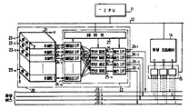
제1도는 본 발명의 일실시예에 관한 화상 처리 장치의 구성을 도시한 블록도.1 is a block diagram showing the configuration of an image processing apparatus according to an embodiment of the present invention.
제2a도 및 제2b도는 제1도에 도시한 메모리 블록 23-i(i=1∼m)의 구성을 설명하는 블록도.2A and 2B are block diagrams for explaining the configuration of the memory blocks 23-i (i = 1 to m) shown in FIG.
제3도 제1도의 화상 처리 장치의 동작을 설명하는 블록도.3 is a block diagram illustrating the operation of the image processing apparatus of FIG.
제4a도 내지 제4c도는 제1도의 화상 처리 장치에 있어서의 화상 데이터의 처리를 설명하는 데이터를 도시한 도면.4A to 4C are diagrams showing data for explaining processing of image data in the image processing apparatus of FIG.
* 도면의 주요부분에 대한 부호의 설명* Explanation of symbols for main parts of the drawings
11 : 제어 회로(CPU) 13 : 화상버스11: control circuit (CPU) 13: image bus
14 : 화상 프로세서 15 : 버스 제어기14: image processor 15: bus controller
20 : 화상 메모리 21 : 3차원 프레임 메모리20: image memory 21: three-dimensional frame memory
22 : 메모리 제어 회로 23 : 메모리 블록22: memory control circuit 23: memory block
25 : 연산 회로 또는 데이터 변환 수단 27 : 제어부25 arithmetic circuit or data conversion means 27 control unit
본 발명은 화상 메모리에 기억되어 있는 화상 데이터를 사용하여 각종 화상 처리를 행하는 화상 처리 장치에 관한 것이다.The present invention relates to an image processing apparatus that performs various image processing using image data stored in an image memory.
일반적으로, 화상 처리 장치는 복수의 화상 메모리를 갖고 있는데, 이 각각의 화상 메모리는 또한 프레임 메모리를 구비하고 있다. 각 프레임 메모리는 1화면을 구성하는 화소에 대하여, 화소마다 그 화소의 농도의 정도를 표시하는 농도 계조 데이터를 기억한다. 화상 프로세서는, 어떤 화상 메모리를 소오스 메모리로 하고 별도의 화상 메모리를 데스티네이션(destination) 메모리로 하여 화상 처리를 행한다.Generally, an image processing apparatus has a plurality of image memories, each of which also has a frame memory. Each frame memory stores density gray scale data indicating the degree of density of each pixel for each pixel constituting one screen. The image processor performs image processing using a certain image memory as a source memory and another image memory as a destination memory.
종래의 화상 처리 장치에서는, 농도 계조 데이터의 비트수가 화상버스의 데이터 비트 길이에 따라서 고정되어 있다. 그리고, 각 프레임 메모리는 고정 비트 길이의 농도 계조 데이터를 기억한다. 이와 같은 화상 처리 장치에서는, 작은 비트수로 표현할 수 있는 농도 계조를 갖는 화상을 처리할 경우, 메모리 공간을 유효하게 사용할 수가 없다. 좀더 구체적으로 설명하면, 처리되는 화상이 2치 화상으로, 농도 계조 데이터가 8비트라고 가정한다. 2치 화상의 농도 계조는 1비트로 표현할 수 있다. 따라서, 농도 계조 데이터의 8비트중 7비트는 실질적으로 사용되지 않고, 프레임 메모리의 메모리 공간의 거의 7/8이 허비된다.In the conventional image processing apparatus, the number of bits of the density gradation data is fixed in accordance with the data bit length of the image bus. Each frame memory stores density grayscale data of fixed bit length. In such an image processing apparatus, when processing an image having a density gray scale that can be represented by a small number of bits, the memory space cannot be effectively used. More specifically, it is assumed that the image to be processed is a binary image and the density gradation data is 8 bits. The density gray level of a binary image can be expressed by 1 bit. Therefore, 7 bits of the 8 bits of the density grayscale data are not substantially used, and almost 7/8 of the memory space of the frame memory is wasted.
이와 같이, 종래의 화상 처리 장치에서는 화상 메모리의 메모리 공간이 유효하게 사용될 수 없는 경우가 많다는 결점이 있었다.As described above, the conventional image processing apparatus has a drawback that the memory space of the image memory cannot be effectively used in many cases.
본 발명의 목적은 화상 메모리 공간을 유효하게 사용할 수 있고, 또 임의의 농도 계조를 갖는 화상을 처리할 수 있는 화상 처리 장치를 제공하는데 있다.It is an object of the present invention to provide an image processing apparatus which can effectively use an image memory space and can process an image having an arbitrary density gray scale.
상기 목적을 달성하기 위하여, 본 발명에 관한 화상 처리 장치는, 독립적으로 액세스 가능한 복수개의 메모리 프레임을 논리적으로 깊이 방향(Z)으로 적층시켜 구성되어, 화상 데이터를 기억하는 3차원 프레임 메모리(21)와; 상기 프레임 메모리(21)에 접속되어, 상기 프레임 메모리(21)의 복수의 임의 영역(A,B,C)을 독립적으로 액세스하며, 상기 복수의 임의 영역(A,B,C)의 각각이 프레임 메모리(21)의 임의의 깊이에 위치하고, 또 깊이 방향으로 임의의 비트수를 갖는 메모리 제어 회로(22)와; 상기 메모리 제어 회로(22)에 접속되어, 화상 데이터를 전송하는 복수의 화상버스(13)와; 상기 복수의 화상버스(13)에 접속되어, 상기 복수의 화상버스(13)중 적어도 하나에서 상기 화상 데이터를 입력하여 연산을 행하고, 그 결과를 상기 복수의 화상버스(13)의 적어도 하나에 출력하는 화상 프로세서와; 상기 메모리 제어 회로(22)와 상기 화상프로세서(14)에 접속되어, 상기 메모리 제어 회로(22)가 액세스 하여야 할 상기 프레임 메모리(21)의 액세스 대상 영역(A,B,C)과 이 액세스 대상 영역마다 액세스의 종류를 상기 메모리 제어 수단(22)에 지정하고, 또 상기 복수의 화상버스(13)를 지정된 영역마다 상기 메모리 버스 회로(22) 및 화상 프로세서(14)에 할당하는 제어 회로(11)를 구비하고 있다.In order to achieve the above object, the image processing apparatus according to the present invention is configured by logically stacking a plurality of independently accessible memory frames in a depth direction Z, and storing a three-dimensional frame memory 21 for storing image data. Wow; Is connected to the frame memory 21 to independently access a plurality of arbitrary regions A, B, and C of the frame memory 21, and each of the plurality of arbitrary regions A, B, and C is a frame. A
상기의 구성으로 함으로써, 본 발명에 관한 화상 처리 장치는, 3차원 프레임 메모리의 메모리 공간을 화상버스의 비트 길이에 제한됨이 없이 깊이 방향으로 임의의 비트수로된 복수의 영역으로 분할하여 사용할 수 있다. 또, 임의의 비트 길이의 화상 데이터를 사용한 화상 처리가 고속으로 행하여진다.With the above configuration, the image processing apparatus according to the present invention can divide and use the memory space of the three-dimensional frame memory into a plurality of regions having an arbitrary number of bits in the depth direction without being limited to the bit length of the image bus. Moreover, image processing using image data of arbitrary bit length is performed at high speed.
이하, 제1도 내지 제4c도를 참조하여 본 발명의 제1실시예에 대한 화상 처리 장치의 구성 및 동작을 설명한다.Hereinafter, the configuration and operation of the image processing apparatus for the first embodiment of the present invention will be described with reference to FIGS. 1 to 4C.
제1도는 본 발명의 일실시예에 관한 화상 처리 장치의 구성을 도시한다. 제1도에 있어서, CPU(11)는 상기 화상 처리 장치의 동작을 제어한다. CPU(11)는 제어 버스(12)에 접속되어 있다. 제어 버스(12)는 CPU(11)가 화상 처리 장치의 각부를 제어하기 위하여 사용하는 각종 제어 정보를 전송한다.1 shows a configuration of an image processing apparatus according to an embodiment of the present invention. In FIG. 1, the
화상버스(13-1∼13-4)는 화상 데이터를 전송한다. 화상버스(13-1∼13-4)의 데이터 비트 길이는 예를들어 8비트가 된다. 화상 프로세서(14)는 제어 버스(12)에 접속된다. 이 화상 프로세서(14)는 제1도에서는 하나이지만, 복수로 하여도 좋다. 화상 프로세서(14)는 예를들면, 2개의 입력 포오트(11,12) 및 하나의 출력 포오트(O)를 갖는다. 화상버스 제어기(15)는 제어 버스(12), 화상 프로세서(14), 화상버스(131-1∼13-4)에 접속된다. 화상버스 제어기(15)는 화상버스(13-1∼13-4)중 어느 하나를 화상 프로세서(14)의 입력 포오트(11)에 접속하고, 화상버스(13-1∼13-4)의 다른 하나를 입력 포오트(12)에 접속하고, 화상버스(13-1∼13-4)의 또 다른 하나를 출력 포오트(O)에 접속한다. 화상버스 제어기(15)는 CPU(11)의 지시에 따라 상기 화상 프로세서(14)의 포오트(11,12.O)와 화상버스(13-1∼13-4)의 접속 관계를 절환시킨다.The image buses 13-1 to 13-4 transfer image data. The data bit length of the image buses 13-1 to 13-4 is, for example, 8 bits. The
화상 메모리(20)는 제어버스(12)와 화상버스(13-1∼13-4)에 접속된다. 제1도에서는 화상 메모리(20)가 하나이지만, 화상 메모리(20)를 복수로 하여도 좋다. 화상 메모리(20)는 3차원 프레임 메모리(21)와; 이 3차원 프레임 메모리(21)에 접속되어 이 3차원 프레임 메모리(21)를 관리하는 메모리 제어기(22)를 갖는다. 3차원 프레임 메모리(21)는 깊이 방향(Z방향)으로, 예를 들어 8×m 비트의 기억 영역을 갖는다(m는 정의 정수이며, 후술하는 메모리 블로수를 의미한다). 3차원 프레임 메모리(21)는 논리적으로 깊이 방향의 소정 비트수로 분할되어 있다. 이 비트수는 화상버스(13-1∼13-4)의 데이터 비트 길이 r과 동등한 비트수이다. 본 실시예에서는, 3차원 프레임 메모리(21)가 깊이 방향으로 8비트 단위의 m개의 메모리 블록으로 분할되어 있다. 즉, 프레임 메모리(21)는 Z방향으로 8비트를 갖는 메모리 블록이 적충되어 있다.The
3차원 프레임 메모리(21)를 메모리 블록마다 제어하는 메모리 제어기(22)는 3차원 프레임 메모리(21)에 접속된다. 메모리 제어기(22)는 메모리 인터페이스(이하, 메모리 I/F라고 칭함)(24-1∼24-m)와; 연사 회로(25-1∼25-4)와; 버스 인터페이스(이하, 버스 I/F/라고 칭함)(26-1∼26-4)와; 제어부(27)을 갖는다. 메모리 I/F(24-1∼24-m)는 메모리 블록(21-1∼21-m)에 설치된다.The
각 메모리 IF(24-1∼24-m)는 대응하는 메모리 불록(23-1∼23-m)에 접속된다. 각 메모리 IF(24-1∼24-m)는 대응하는 메모리 블록(21-1∼21-m)의 리드 액세스(read access) 또는 라이트 액세스(write access)를 행한다.Each memory IF 24-1 to 24-m is connected to a corresponding memory block 23-1 to 23-m. Each memory IF 24-1 to 24-m performs read access or write access to the corresponding memory blocks 21-1 to 21-m.
연산 회로(25-1∼25-4)는 화상버스(13-1∼13-4)마다 설치된다. 연산회로(25-1∼25-4)의 각각은 메모리 I/F(24-1∼25-4)에 접속된다. 각 연산회로(25-1∼25-4)가 리드 동작인 경우에는 프레임 메모리(21)에서 판독된 데이터에 소정의 연산을 실시하고 화상버스(13-1∼13-4)에 출력되는 데이터를 생성한다. 각 연산 회로(25-1∼25-4)가 라이트 동작인 경우에는 화상버스(13-1∼13-m)에서 받은 데이터에 소정의 연산을 실시하고, 3차원 프레임 메모리(21)에 기입되는 데이터를 생성한다. 버스 I/F(26-1∼26-4)는 화상버스(13-1∼13-4)마다 설치된다.The calculation circuits 25-1 to 25-4 are provided for each of the image buses 13-1 to 13-4. Each of the arithmetic circuits 25-1 to 25-4 is connected to the memory I / Fs 24-1 to 25-4. When each of the calculation circuits 25-1 to 25-4 is a read operation, a predetermined calculation is performed on the data read from the frame memory 21, and the data output to the image buses 13-1 to 13-4 is read. Create When each of the calculation circuits 25-1 to 25-4 is a write operation, a predetermined calculation is performed on the data received from the image buses 13-1 to 13-m, and the data is written to the three-dimensional frame memory 21. Generate data. The bus I / Fs 26-1 to 26-4 are provided for each of the image buses 13-1 to 13-4.
각 버스 I/F(26-1∼26-4)는 대응하는 연산 회로(25-1∼25-4)와 대응하는 버스(13-1∼13-4)에 접속되어 있다. 버스 I/F(26-1∼26-4)는 화상버스(13-1∼13-4)와 연산 회로(25-1∼25-4)사이의 데이터 수신을 행한다.Each bus I / F 26-1 to 26-4 is connected to corresponding arithmetic circuits 25-1 to 25-4 and corresponding buses 13-1 to 13-4. The buses I / Fs 26-1 to 26-4 receive data between the image buses 13-1 to 13-4 and the calculation circuits 25-1 to 25-4.
제어부(27)는 CPU(11)에서의 지시에 따라서, 메모리 I/F(24-1∼24-m), 연산 회로(25-1∼25-4) 및 버스 I/F(26-1∼26-4)를 제어한다. 구체적으로, 제어부(27)는 메모리 I/F(24-1∼24-m)중에서 하나 또는 복수개를 선택하고; 선택한 메모리 I/F(24-1∼24-m)에 리드 모드 및 라이트 모드를 지정하고; 선택한 메모리 I/F(24-1∼24-m)에 3차원 프레임 메모리(21)내로 액세스 하여야할 영역을 지정하는 등의 동작을 행한다. 제어부(27)는 연산 회로(25-1∼25-4)에 그 연산에 필요한 정보 및 명령등을 공급한다. 제어부(27)는 버스 I/F(26-1∼26-4)에 데이터의 흐름 방향을 표시하는 명령등을 공급한다. 또, 메모리 제어기(22)는 별개의 부품으로 구성되어도 좋다. 또 메모리 제어기(22)로서 CPU와 주변 회로를 준비하고, 메모리 제어기(22)의 동작을 소프트웨어로 처리하는 것도 가능하다. 동작 속도를 문제로 하지 않으면, CPU(11)를 메모리 제어기로서 사용해도 좋다.The
CPUI(11)의 동작에 사용되는 프로그램, 고정 데이터등을 기억하는 ROM(도시생략)이 제어버스(12)에 접속된다. CPU(11)와 키보오드, 호스트 컴퓨터 등과 같은 외부 장치간의 데이터의 수신을 제어하는 인터페이스(도시생략)가 제어 버스(12)에 접속된다.A ROM (not shown) for storing a program, fixed data, and the like used for the operation of the
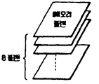
다음에, 3차원 프레임 메모리(21)의 하나인 메모리 블록(23-i; i=1,2,…m)의 구성을 제2a도 및 제2b도를 참조하여 설명한다. 본 실시예에 있어서, 메모리 블록(23-i)은 제2a도에 도시한 바와 같이 메모리 프레임을 논리적인 8개의 깊이 방향으로 구성되게 한다. 각 메모리 프레임은 깊이 방향으로 1비트의 기억용량을 갖고 XY 평면상에 1화면의 화소의 수에 대응하는 비트 수의 기억 용량을 가지며, 또 1화면을 구성하는 전 화소에 대하여 각 화소의 농도 계조 데이터의 1비트를 기억한다.Next, the configuration of the memory block 23-i (i = 1, 2, ... m), which is one of the three-dimensional frame memories 21, will be described with reference to FIGS. 2A and 2B. In this embodiment, the memory block 23-i causes the memory frame to be configured in eight logical depth directions as shown in FIG. 2A. Each memory frame has a storage capacity of 1 bit in the depth direction and a storage capacity of the number of bits corresponding to the number of pixels of one screen on the XY plane, and the density gradation of each pixel for all pixels constituting one screen. Stores one bit of data.
구체적으로 말하자면, 메모리 블록(23-i)은 제2b도에 도시한 바와 같이, 8개의 메모리 칩(30-0∼30-7)으로 구성된다. 각 메모리 칩(30-0∼30-7)은 1화면의 전 화소에 대하여, 각 화소의 농도 계조 데이터중의 1비트를 기억한다. 이 메모리 칩(30-0∼30-7)의 어드레스 단자(A0-An)에는, 메모리 I/F(24-i; i=1,2,…m)에서 출력되는 공통 어드레스가 유도된다. 상기 메모리 칩(30-0∼30-7)의 칩 인에이블 단자 CE에는 메모리 I/F(24-i; i=1,2,…m)에 출력되는 칩 선택 신호(C0∼C7)가 유도된다. 따라서, 메모리 I/F(24-i)는 메모리 칩(30-0∼30-7)을 그 칩의 단위로 선택할 수 있다. 메모리 칩(30-0∼30-7)의 R/W단자에는, 메모리 I/F(24-i; i=1,2,…m)에서 공통 R/W 신호가 유도된다. 따라서, 메모리 칩(30-1∼30-7)은 총괄적으로 리드 모드 또는 라이트 모드에 설정된다. 메모리 칩(30-0∼30-7)의 데이터 단자 D는 메모리 I/F(24-i; i=1,2,…m)의 데이터 단자(D0∼D7)에 접속된다.Specifically, the memory block 23-i is composed of eight memory chips 30-0 to 30-7, as shown in FIG. 2B. Each memory chip 30-0 to 30-7 stores one bit of density grayscale data of each pixel for all the pixels on one screen. The common addresses output from the memory I / F (24-i; i = 1, 2, ... m) are derived to the address terminals A0-An of the memory chips 30-0 to 30-7. Chip select signals C0 to C7 output to the memory I / F (24-i; i = 1, 2, ... m) are guided to the chip enable terminals CE of the memory chips 30-0 to 30-7. do. Therefore, the memory I / F 24-i can select the memory chips 30-0 to 30-7 in units of the chips. The common R / W signal is guided to the R / W terminals of the memory chips 30-0 to 30-7 in the memory I / F (24-i; i = 1, 2, ... m). Therefore, the memory chips 30-1 to 30-7 are collectively set in the read mode or the write mode. The data terminals D of the memory chips 30-0 to 30-7 are connected to the data terminals D0 to D7 of the memory I / F (24-i; i = 1, 2, ... m).
본 실시예에 관한 화상 처리 장치의 동작을 설명한다. 우선, 처음에는 메모리 제어기(22)의 동작을 설명하고 다음에 그 장치 전체의 동작을 설명한다. 본 실시예에 있어서, CPU(11)는 화상버스(13-1∼13-4)마다 프레임 메모리(21)의 리드 동작과 라이트 동작을 따로 지정할 수가 있다. CPU(11)은 3차원 프레임 메모리(21)에 대한 Z방향의 임의의 p비트째에서 시작하여 임의의 q비트의 데이터를 액세스하는 것을 지정할 수 있다. 여기에서, p는 0∼8×m-1, q는 1∼8의 범위를 취할 수 있다. q는 예를 들어 농도 계조 데이터의 비트수이다. 실제로 액세스되는 메모리 블록(23-i)은, i의 값이 다음식으로 표시되는 메모리 블록이 된다.The operation of the image processing apparatus according to the present embodiment will be described. First, the operation of the
i=[p/8]+1∼[(p+q-1)/8]+1(i은 정수)i = [p / 8] +1 to [(p + q-1) / 8] +1 (i is an integer)
단, 아래의 설명에서는 이해를 용이하게 하기 위하여, CPU(11)가 리드/라이트이 대상이 되는 메모리 블록(복수의 메모리 블록이 액세스될 때에는 선두의 메모리 블록)도 지정하는 것으로 한다. 그리고 상기 p는 선두 메모리 블록내의 선두 비트의 위치를 표시하는 것으로 한다. 이 경우, p는 0∼7의 값을 취한다.However, in the following description, for ease of understanding, the
메모리 제어기(22)의 동작은 다음의 A∼D의 4개의 경우, 즉, A : 1개의 메모리 블록에 대한 리드, B : 2개의 메모리 블록에 대한 리드, C : 1개의 메모리 블록에 대한 라이트, D : 2개의 메모리 블록에 대한 라이트로 나눌 수 있다. 이하, 상기 A∼D의 동작을, 화상버스(13-1)를 소오스 혹은 데스티네이션 버스로서 사용할 경우를 예로 하여 설명한다.The operation of the
A : 1개의 메모리 블록에 대한 리드.A: Read for one memory block.
메모리 블록(23-i)의 비트p(0![]()
![]()
![]()
![]()
![]()
![]()
![]()
![]()
![]()
![]()
![]()
![]()
(1) CPU(11)에서의 명령을 받아서, 제어부 (27)은 메모리 블록(23-i)을 액세스 하는 것으로 판단하고, 메모리 I/F(24-i)에 리드 액세스를 지시한다. 또, 제어부(27)는 리드 액세스인 p, q의 값등을 연산회로(24-1)에 지시한다. 또, 제어부(27)는 리드 액세스를 버스 I/F(25-1)에 지시한다.(1) In response to the command from the
메모리 I/F(24-i)는 병렬 메모리 블록(23-i)의 8비트를 리드한다. 메모리 I/F(24-1)는 판독한 데이터를 화상버스(13-1)에 대응하는 연산회로(25-1)로 출력한다.Memory I / F 24-i reads 8 bits of parallel memory block 23-i. The memory I / F 24-1 outputs the read data to the arithmetic circuit 25-1 corresponding to the image bus 13-1.
(2) 연산회로(25-1)는 메모리 I/F(24-i)에 의하여 리드된 8비트 데이터를 p비트 LSB 방향으로 시프트 한다. 다음에 연산회로(25-1)는 시프트된 데이터의 q+1비트 이상의 각 비트를 "0"으로 하여 버스 I/F(26-1)로 출력한다. 예를들면, 메모리 블록(23-i)에 유지된 데이터가(MSB)"11011011"(LSB), p=2, q=4인 경우, 연산회로는 그 데이터를 2비트 시프트하여 "00110110"을 생성하고, 제 4비트 이상에는 0데이타를 기입하고, 데이터"00000110"을 출력한다.(2) The calculation circuit 25-1 shifts 8-bit data read by the memory I / F 24-i in the p-bit LSB direction. Next, the arithmetic circuit 25-1 outputs to the bus I / F 26-1 each bit of q + 1 bit or more of the shifted data as " 0 ". For example, when the data held in the memory block 23-i is (MSB) # 11011011_ (LSB), p = 2, q = 4, the arithmetic circuit shifts the data by two bits to obtain " 00110110 " 0 data is written to the fourth bit or more, and data # 00000110 \ is output.
(3) 버스 I/F(26-1)는 연산회로(25-1)에서 출력되는 8비트 데이터를 화상버스(13-1)에 출력한다.(3) The bus I / F 26-1 outputs 8-bit data output from the arithmetic circuit 25-1 to the image bus 13-1.
B : 2개의 메모리 블록에 대한 리드(2개의 메모리 블록에 걸친 영역의 리드)B: reads for two memory blocks (read of area across two memory blocks)
메모리 블록(23-i)은 비트 p(1![]()
![]()
![]()
![]()
![]()
![]()
![]()
![]()
![]()
![]()
(1) CPU(11)에서의 명령을 받고, 제어부(27)는 메모리 블록(23-i, 23-(i+1))을 액세스하는 것으로 판단하고, 메모리 I/F(24-i, 24-(i+1))에 리드 액세스를 지시한다. 또, 제어부(27)는 리드 액세스인 q, p의 값등을 연산회로(24-1)에 지시한다. 또, 제어부(27)는 리드 액세스를 버스 I/F(25-1)에 지시한다.(1) Upon receiving a command from the
메모리 I/F(24-i, 24-(i+1))는 메모리 블록(23-i, 23-(i+1))에서 각각 8비트 데이터를 리드하여 연산회로(25-1)에 출력한다.The memory I / F (24-i, 24- (i + 1)) reads 8-bit data from the memory blocks 23-i and 23- (i + 1), respectively, and outputs them to the operation circuit 25-1. do.
(2) 연산회로(25-1)는 메모리블록(23-i)에서 판독된 8비트 데이터를 p비트 LSB 방향으로 시프트하고, 비트 8-p이상의 각 비트를 "0"으로 한다. 연산회로(25-1)는 메모리 블록(23-(i+1))에서 판독된 8비트 데이터를 8-p 비트 MSB 방향으로 시프트하고, 또, 비트 7-p이하의 각 비트 및 비트 q이상의 각 비트를 "0"으로 한다. 연산회로(25-1)는 생성된 2개의 데이터의 OR을 취하여 버스 I/F(26-1)에 출력한다.(2) The arithmetic circuit 25-1 shifts the 8-bit data read out from the memory block 23-i in the p-bit LSB direction and sets each bit of bit 8-p or more to '0'. The arithmetic circuit 25-1 shifts the 8-bit data read out from the memory block 23- (i + 1) in the 8-p bit MSB direction, and each bit of the bit 7-p or less and the bit q or more. Set each bit to '0'. The calculation circuit 25-1 takes the OR of the two generated data and outputs the OR to the bus I / F 26-1.
예를 들어, p가 5, q가 6으로, 메모리 블록 23-i에서 데이터(MSB) "10011001"(LSB), 메모리 블록(23-(i+1))에서 데이터 "10011001"이 판독되었다고 가정할 경우, 연산회로는 데이터 "00000100"과 데이터 "00001000"을 생성하고, 양데이타의 논리화를 취하여, 데이터 "00001100"을 화상버스(13-1)에 출력한다.For example, suppose that p is 5 and q is 6, and data # 10011001 \ is read from data MSB # 10011001 \ (LSB) and memory block 23- (i + 1) in memory block 23-i. In this case, the arithmetic circuit generates data # 00000100 'and data # 00001000 \, takes the logic of both data, and outputs data # 00001100 \ to the image bus 13-1.
(3) 버스 I/F(26-1)는 연산회로(25-1)에서 출력된 8비트 데이터를 버스(13-1)에 출력한다.(3) The bus I / F 26-1 outputs 8-bit data output from the arithmetic circuit 25-1 to the bus 13-1.
C : 1개의 메모리 블록에 대한 라이트.C: Write to one memory block.
메모리 블록(23-i)의 비트 p(0![]()
![]()
![]()
![]()
![]()
![]()
![]()
![]()
![]()
![]()
![]()
![]()
(1) CPU(11)에서 명령을 받아서, 제어부(27)는 메모리 블록(23-i)을 액세스 하는 것으로 판단하고, 메모리 I/F(24-i)에 라이트 액세스를 지시한다. 또, 제어부(27)는 라이트 액세스인 p, q의 값등을 연산회로(24-1)에 지시한다. 또, 제어부(27)는 라이트 액세스를 버스 I/F(25-1)에 지시한다. 우선, 버스 I/F(26-1)는 화상버스(13-1)에서 8비트 데이터를 입력하여 연산회로(25-1)에 출력한다.(1) Upon receiving an instruction from the
(2) 연산회로(25-1)는 입력데이타를 MSB측으로 p비트 시프트하여, 메모리 I/F(24-i)에 출력한다.(2) The arithmetic circuit 25-1 shifts the input data p-bits to the MSB side and outputs it to the memory I / F 24-i.
(3) 메모리 I/F(24-1)는 칩 선택신호 Cp∼Cp+q-1을 액티브로 하고, 연산회로(25-1)에서 출력된 8비트 데이터중의 비트 p에서 개시하는 q비트를 메모리 블록(23-i)의 해당 영역에 라이트한다.(3) The memory I / F 24-1 activates the chip select signals Cp to Cp + q-1 and starts q bits starting from bit p of 8-bit data output from the arithmetic circuit 25-1. Is written into the corresponding area of the memory block 23-i.
예를들어, p가 2, q가 4이고, 화상버스(13-1)에 데이터 "10101010"이 출력되는 경우, 연산회로(24-1)는 데이터 "10101000"을 출력한다. 메모리(24-1)은 칩 선택신호 C2 C5를 액티브로 하고, 메모리칩(30-2∼30-5)에 데이터 "1010"을 라이트한다.For example, when p is 2 and q is 4, and data # 10101010 'is output to the image bus 13-1, the calculation circuit 24-1 outputs data # 10101000'. The memory 24-1 activates the chip select signal C2 C5 and writes the data # 1010 'to the memory chips 30-2 to 30-5.
D : 2개의 메모리 블록에 대한 라이트.D: Write to two memory blocks.
메모리 블록(23-i)의 비트 p(1![]()
![]()
![]()
![]()
![]()
![]()
![]()
![]()
![]()
![]()
(1) CPU(11)에서의 명령을 받고, 제어부(27)는 메모리 블록(23-i, 23-(i+1))을 액세스하는 것으로 판단하고, 메모리 I/F(24-1, 24-1(i+1))에 리드 액세스인 것을 지시한다. 또, 제어부(27)는 리드 액세스인 q, p의 값등을 연산회로(24-1)에 지시한다. 또, 제어부(27)는 리드 액세스를 버스 I/F(26-1)에 지시한다.(1) Upon receiving an instruction from the
우선, 버스 I/F(26-1)는 화상버스(13-1)에서 8비트 데이터를 입력하여 연산회로(25-1)에 출력한다.First, the bus I / F 26-1 inputs 8-bit data from the image bus 13-1 and outputs it to the calculation circuit 25-1.
(2) 연산회로(25-1)는 입력데이타를 p비트 MSB 방향으로 시프트하여 얻어진 8비트 데이터를 메모리 I/F(24-i)에 출력한다. 연산회로(25-1)는 입력 데이터를 8-p 비트 LSB 방향으로 시프트하여 얻어지는 8비트 데이터를 메모리 I/F(24-(i+1))에 출력한다.(2) The calculation circuit 25-1 outputs 8-bit data obtained by shifting the input data in the p-bit MSB direction to the memory I / F 24-i. The calculation circuit 25-1 outputs 8-bit data obtained by shifting the input data in the 8-p bit LSB direction to the memory I / F 24- (i + 1).
(3) 메모리 I/F(24-i)는 칩 선택신호 Cp∼C7을 액티브 레벨로 하고, 연산회로(25-1)에서 출력된 8비트 데이터중의 비트 p에서 시작하는 8-p 비트를, 메모리 I/F(24-(i+1))는 칩 선택 신호 C0-Cp+q-8을 액티브 레벨로 하고, 연산회로(25-1)에서 출력된 8비트 데이터중의 비트 0에서 개시하는 p+q-8 비트를, 메모리 블록(23-(i+1))의 해당 영역에 라이트 한다.(3) The memory I / F 24-i sets the chip select signals Cp to C7 as active levels, and selects 8-p bits starting from bit p of 8-bit data output from the arithmetic circuit 25-1. The memory I / F (24- (i + 1)) sets the chip select signal C0-Cp + q-8 as the active level and starts at
예를 들면, p가 6, q가 4이고, 화상버스(13-1)에 데이터 "10101010"이 출력되는 경우, 연산회(25-1)는 데이터 "10000000"을 메모리 I/F(24-(i+1))에 데이터 "00000010"을 출력한다. 메모리 I/F(24-1)는 칩 선택신호 C6, C7을 액티브로 하고, 메모리 칩(30-6, 30-7)에 데이터 "10"을 라이트한다. 메모리 I/F(24-(i+1))는 칩 선택신호 C0, C1을 액티브로 하여, 메모리 칩(30-0, 30-1)에 데이터 "10"을 라이트한다.For example, when p is 6 and q is 4, and the data # 10101010 \ is output to the image bus 13-1, the arithmetic meeting 25-1 returns the data # 10000000 \ by the memory I / F (24-). (i + 1)) outputs data # 00000010 '. The memory I / F 24-1 activates the chip select signals C6 and C7, and writes the data # 10 'to the memory chips 30-6 and 30-7. The memory I / F 24- (i + 1) activates the chip select signals C0 and C1 to write the data # 10 'to the memory chips 30-0 and 30-1.
다음에, 본 실시예에 관한 화상처리 장치 전체의 동작을 제3도 내지 제4c도를 참조하여, "3차원 프레임 메모리(21)의 영역 A와 영역 B에 기억된 화상 데이터의 AND를 위하여 새로운 화상 데이터를 구하고, 그 화상 데이터를 3차원 프레임 메모리(21)의 영역 C에 기억되는 경우"에 대해 설명한다.Next, the operation of the entire image processing apparatus according to the present embodiment will be described with reference to FIGS. 3 to 4C, for the AND of the image data stored in the area A and the area B of the 3D frame memory 21. The case where image data is obtained and the image data is stored in the area C of the three-dimensional frame memory 21 will be described.
이러한 설명을 위하여, 영역 A를 메모리 블록(23-1)의 비트 1에서 Z방향으로의 6비트분의 영역과, 영역 B를 메모리 블록(23-2)의 비트 6에서 Z방향으로의 6비트분의 영역과, 그리고 영역 C를 메모리 블록(23-m)의 비트 1에서 시작되는 6비트분의 영역을 가정한다. 또 영역 A에서의 화상 데이터의 데스티네이션 버스로서 화상버스(13-1)를, 영역 B에서의 화상 데이터의 데스티네이션 버스로서 화상버스(13-2)를, 그리고 영역 C에서의 화상 데이터의 소오스 버스로서 화상버스(13-4)를 할당하는 것으로 가정한다. 또, 화상프로세서(14)의 포오트(11,12)에 화상버스(13-1, 13-2)를, 포오트(O)에 화상버스(13-4)를 각각 할당하는 것으로 가정한다.For this description, the area A is 6 bits in the Z direction in the
CPU(11)는 동작의 내용을 지시하는 명령, 즉 화상버스(13-1∼13-4)중 어떤 것을 영역 A∼C에 할당하는지를 지시하는 명령을 제어부(27)에 출력한다. 또, CPU(11)는 화상 프로세서(14)에 AND연산을 지정하고, 화상프로세서(14)를 동작시킨다.The
제어부(27)는 CPU(11)에서의 명령을 받아서, 제3도에 도시한 바와 같이 메모리 I/F(24-1 24-3)에는 리드 동작을, 메모리 I/F(24-m)에는 라이트 동작을 지시한다. 또, 제어부(27)는 연산회로(25-1)에는 메모리 I/F(24-1)에서의 데이터에 대한 연산을, 연산회로(25-2)는 메모리 I/F(24-2, 24-3)에서의 데이터에 대한 연산을 지시하여, 필요한 데이터를 공급한다. 또, 제어부(27)는 버스 I/F(26-1, 26-2)에 리드 동작, 버스 I/F(26-4)에 라이트 동작을 지시한다.The
이상의 세팅에 응답하여, 영역 A에 대하여는 상기 A에 표시한 리드 처리(단 p=1, q=6)를, 영역 B에 대하여는 상기 B에 표시한 리드처리(단 p=6, q=6)를, 그리고 영역 C에 대하여는 상기 C에 표시한 라이트처리(단 p=1, q=6)를 행하게 된다. 각 영역에 관한 처리를 순서적으로 설명한다.In response to the above setting, the read processing (where p = 1, q = 6) shown in the above A for the area A, and the read processing (where p = 6, q = 6) shown in the above B for the area B And the area C is subjected to the write processing (where p = 1, q = 6) indicated in the above C. Processing relating to each area will be described in order.
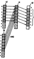
영역 A에 대한 처리는 다음과 같이 행하여진다. 메모리 I/F(24-1)는 제1의 화소 Pa의 어드레스를 출력하고, R/W 신호를 라이트 인에이블에 설정하고, 칩 선택신호 C0∼C7을 전부 액티브 레벨로 하여, 영역 A에서 제1의 화소에 관한 데이터(41)를 판독한다. 메모리 I/F(24-1)는 판독한 8비트 데이트(41)를 연산회로(25-1)에 출력한다. 연산회로(25-1)는 데이터(41)을 제4a도에 도시한 바와 같이 1(=p)비트 LSB 방향으로 시프트하고, 또 비트 6(=q)이상의 비트에 "0"을 대입한다. 연산회로(25-1)는 생성한 데이터(42)를 버스 I/F(26-1)에 출력한다. 버스 I/F(26-1)는 데이터(42)를 화상버스(13-1)에 출력한다. 데이터(42)는 화상버스 제어기(15)를 통하여 화상 프로세서(14)이 입력 포오트(11)에 공급된다.The processing for the area A is performed as follows. The memory I / F 24-1 outputs the address of the first pixel Pa, sets the R / W signal to write enable, sets all the chip select signals C0 to C7 as the active level, and generates the first pixel Pa.
영역 B에 대한 처리는 다음과 같이 행해진다. 즉 메모리 I/F(24-2, 24-3)는 메모리 블록(23-2, 23-3)에서 데이터(51,52)를 각각 판독하고, 연산회로(25-2)에 출력한다. 연산회로(25-2)는 데이터(51)를 제4b도에 도시한 바와 같이 6(=q)비트 LSB 방향으로 시프트하고, 또 비트 2(=8-p)이상의 각 비트를 "0"으로 하여 데이터(53)으로 변환한다. 마찬가지로, 연산회로(25-2)는, 메모리 I/F(24-3)에 의하여 리드된 데이터(52)를 2(8-p) 비트 MSB 방향으로 시프트하고, 또 비트 1(=7-p)이하의 각 비트 및 비트 6(=q)이상의 각 비트를 "0"으로 하여, 데이터(54)로 변경한다. 연산회로(25-2)는 데이터(52, 53)의 논리화를 취하여 데이터(55)를 생성하고, 버스, I/F(26-2)로 출력한다. 버스 I/F(26-2)는 데이터(55)를 화상버스(13-2)에 출력한다. 데이터(55)는, 화상버스 제어기(15)를 통하여 화상 프로세서(14)의 입력 포오트(12)에 공급된다.The processing for the area B is performed as follows. That is, the memory I / Fs 24-2 and 24-3 read the
화상 프로세서(14)는 입력 포오트(11,12)에 공급된 8비트 데이터(42)와, 8비트 데이터(55)에 제4c도 도시한 바와 같이 AND 연산을 실시한다. 상기 AND 연산에 의하여 생성된 데이터(61)는 출력단자(O)를 통하여 화상버스 제어기(15)에 공급된다. 화상버스 제어기(15)는 데이터(61)을 화상버스(13-4)에 출력한다.The
영역 C에 대한 처리는 이하의 순서로 행하여진다. 버스 I/F(26-4)는 화상버스(13-4)에서 데이터(61)을 받아, 연산회로(25-4)에 공급한다. 연산회로(25-4)는 데이터(61)을, 제4c도에 도시한 바와 같이 MSB 방향에서 1(=p)비트 시프트하여 영역 C에 기억되어야할 데이터(비트 1∼비트 6)을 포함하는 데이터(62)로 변환한다. 연산회로(25-4)는 변환된 데이터를 메모리 I/F(24-m)에 출력한다. 메모리 I/F(24-m)는 R/W 신호를 라이트 인에이블로 설정하고, 칩 선택신호 C1 C6를 액티브로 하며, 칩 선택신호 C0, C7을 비액티브로 하고, 또 제1의 화소 Pa의 어드레스를 출력하여 연산회로(25-4)에서 출력되는 데이터(62)중의 비트 1∼비트 6의 6비트를 영역 C에 라이트 한다.Processing for the area C is performed in the following order. The bus I / F 26-4 receives the data 61 from the image bus 13-4 and supplies it to the arithmetic circuit 25-4. The calculation circuit 25-4 includes data (
본 실시예에서는 메모리 블록(23-m)을 구성하는 메모리 칩내의 영역 C에서 벗어난 영역을 구성하는 메모리 칩(30-1, 30-m)의 기억내용이 파괴되는 것이 방지된다.In this embodiment, the storage contents of the memory chips 30-1 and 30-m constituting the region deviating from the region C in the memory chip constituting the memory block 23-m are prevented from being destroyed.
제1의 화소 Pa에 대하여 이상의 동작이 종료되면, 다음의 제2의 화소 Pb에 대해 동일한 동작이 행하여진다. 이하, 동일한 동작, 즉 독출 기입 독출 기입의 반복적 동작이 파이프라인 방식으로 연속적으로 행하여지고, 모든 화소에 대하여 영역 A, B에 기억된 화상 데이터간의 AND 연산에 의하여 구해진 화상 데이터가 영역 C에 기억되면, CPU(11)는 메모리 제어기(22) 및 화상버스 제어기(15)에 대한 화상버스 할당을 해제한다.When the above operation is completed for the first pixel Pa, the same operation is performed for the next second pixel Pb. Hereinafter, if the same operation, that is, the repetitive operation of read-write read-write, is continuously performed in a pipelined manner, and image data obtained by the AND operation between the image data stored in areas A and B for all the pixels is stored in the area C. The
이상의 설명에서는, 화상 데이터가 6비트인 경우에 대하여 설명하였다. 본 발명은 화상버스(13-1∼13-4)의 데이터 길이를 상한으로 하는 임의의 비트수의 화상 데이터에 대하여 적용시킬 수 있다. 또, 리드 데이터와 라이트 데이터와는, 동이 비트 길이일 필요는 없다. 예를들면, 본 발명은 상기 2개의 6비트 화상 데이터(42, 55)의 AND 데이터(61)를 소정의 스테이트 홀드값을 경계로 하여 2진화하고 얻어진 데이터(1비트)를 프레임 메모리(21)에 기억시킬 경우에도 적용할 수 있다.In the above description, the case where the image data is 6 bits has been described. The present invention can be applied to image data of any number of bits having the upper limit as the data length of the image buses 13-1 to 13-4. In addition, the read data and the write data need not be the same bit length. For example, the present invention binarizes the AND data 61 of the two 6-
상기 실시예에서는, 화상 데이터를 농도계조 데이터의 경우를 예로하여 설명하였으나, 본 발명은 3차원 메모리에 기억된 데이터를 처리하는 모든 경우에 응용 가능하다. 3차원 프레임 메모리(21)에 기억된 화상은, 2치 혹은 다치의 2차원 화상에 국한되는 것은 아니다. 예를들면, 3차원 프레임 메모리(21)에는 3차원의 2치화상을 기억하는 것도 가능하다. 이 경우, 3차원의 2치화상 처리(AND, OR 등의 논리연산, 주변분포, 논리 필터링 등)을, 상기 2차원 화상의 처리와 동일하게 하여, 2차원인 화상 프로세서(14)로 행할 수 있다. 또, 상기 실시예에서는, 제1의 화소 Pa에서 순번으로 처리를 행하였으나, 처리의 순번은 임의로 할 수 있다.In the above embodiment, the image data has been described taking the case of density gradation data as an example, but the present invention is applicable to all cases of processing data stored in the three-dimensional memory. The image stored in the three-dimensional frame memory 21 is not limited to two-dimensional or multi-value two-dimensional images. For example, it is also possible to store a three-dimensional binary image in the three-dimensional frame memory 21. In this case, three-dimensional binary image processing (logical operations such as AND and OR, peripheral distribution, logical filtering, etc.) can be performed by the two-
본 발명에 의하면, 화상 데이터의 비트수는 화상버스의 비트수에만 고정되지 않고, 임의로 선택할 수 있다. 따라서, 3차원 프레임 메모리(21)의 메모리 공간을 깊이방향(Z 방향)으로 임의의 비트 길이의 복수 영역으로 분할하여 사용할 수 있다. 그러므로, 메모리 공간을 유효하게 사용할 수 있고, 화상 데이터의 비트수가 고정되어 있을 경우에 비하여, 다수의 2차원 화상을 화상 메모리에 격납시킬 수가 있다. 또, 프레임 메모리에 2치의 3차원 화상을 기억시켰을 때에는, 3차원 화상의 처리를 2차원인 화상 프레세서로 행할 수도 있다.According to the present invention, the number of bits of the image data is not fixed only to the number of bits of the image bus, but can be arbitrarily selected. Therefore, the memory space of the three-dimensional frame memory 21 can be divided into a plurality of regions having arbitrary bit lengths in the depth direction (Z direction). Therefore, the memory space can be used effectively, and a large number of two-dimensional images can be stored in the image memory as compared with the case where the number of bits of the image data is fixed. When a two-dimensional three-dimensional image is stored in the frame memory, the three-dimensional image may be processed by a two-dimensional image processor.
Claims (12)
Applications Claiming Priority (2)
| Application Number | Priority Date | Filing Date | Title |
|---|---|---|---|
| JP62-78590 | 1987-03-31 | ||
| JP62078590A JPS63245567A (en) | 1987-03-31 | 1987-03-31 | Picture processor |
Publications (2)
| Publication Number | Publication Date |
|---|---|
| KR880011688A KR880011688A (en) | 1988-10-29 |
| KR920002468B1 true KR920002468B1 (en) | 1992-03-26 |
Family
ID=13666125
Family Applications (1)
| Application Number | Title | Priority Date | Filing Date |
|---|---|---|---|
| KR1019880003554A KR920002468B1 (en) | 1987-03-31 | 1988-03-31 | Image processing apparatus |
Country Status (4)
| Country | Link |
|---|---|
| US (1) | US4943937A (en) |
| JP (1) | JPS63245567A (en) |
| KR (1) | KR920002468B1 (en) |
| DE (1) | DE3811145A1 (en) |
Families Citing this family (14)
| Publication number | Priority date | Publication date | Assignee | Title |
|---|---|---|---|---|
| US5254979A (en) * | 1988-03-12 | 1993-10-19 | Dupont Pixel Systems Limited | Raster operations |
| USRE39529E1 (en) * | 1988-04-18 | 2007-03-27 | Renesas Technology Corp. | Graphic processing apparatus utilizing improved data transfer to reduce memory size |
| US5068650A (en) * | 1988-10-04 | 1991-11-26 | Bell Communications Research, Inc. | Memory system for high definition television display |
| US5083257A (en) * | 1989-04-27 | 1992-01-21 | Motorola, Inc. | Bit plane partitioning for graphic displays |
| US5233690A (en) * | 1989-07-28 | 1993-08-03 | Texas Instruments Incorporated | Video graphics display memory swizzle logic and expansion circuit and method |
| US5555460A (en) * | 1989-11-29 | 1996-09-10 | Chips And Technologies, Inc. | Method and apparatus for providing a reformatted video image to a display |
| JPH0416996A (en) * | 1990-05-11 | 1992-01-21 | Mitsubishi Electric Corp | Display device |
| FR2677206A1 (en) * | 1991-05-31 | 1992-12-04 | Philips Electro Grand Public | DEVICE FOR VISUALIZING PARTIAL VIEWS OF AN IMAGE. |
| US5404448A (en) * | 1992-08-12 | 1995-04-04 | International Business Machines Corporation | Multi-pixel access memory system |
| US5659631A (en) | 1995-02-21 | 1997-08-19 | Ricoh Company, Ltd. | Data compression for indexed color image data |
| DE69731493T2 (en) * | 1996-05-28 | 2005-03-24 | Matsushita Electric Industrial Co., Ltd., Kadoma | Analog FIFO memory |
| US6551857B2 (en) | 1997-04-04 | 2003-04-22 | Elm Technology Corporation | Three dimensional structure integrated circuits |
| JP5388323B2 (en) * | 2007-11-09 | 2014-01-15 | 独立行政法人 宇宙航空研究開発機構 | calculator |
| CN114171092A (en) * | 2020-04-23 | 2022-03-11 | 长江存储科技有限责任公司 | Memory device and programming method thereof |
Family Cites Families (8)
| Publication number | Priority date | Publication date | Assignee | Title |
|---|---|---|---|---|
| ZA757388B (en) * | 1974-12-16 | 1977-07-27 | Photovoltaic Ceramic Corp | Ferroelectric ceramic devices |
| US4564915A (en) * | 1980-04-11 | 1986-01-14 | Ampex Corporation | YIQ Computer graphics system |
| JPS5837948A (en) * | 1981-08-31 | 1983-03-05 | Toshiba Corp | Laminated semiconductor memory device |
| GB8306339D0 (en) * | 1982-03-19 | 1983-04-13 | Quantel Ltd | Video processing systems |
| US4800380A (en) * | 1982-12-21 | 1989-01-24 | Convergent Technologies | Multi-plane page mode video memory controller |
| US4742474A (en) * | 1985-04-05 | 1988-05-03 | Tektronix, Inc. | Variable access frame buffer memory |
| US4725987A (en) * | 1985-10-23 | 1988-02-16 | Eastman Kodak Company | Architecture for a fast frame store using dynamic RAMS |
| US4745407A (en) * | 1985-10-30 | 1988-05-17 | Sun Microsystems, Inc. | Memory organization apparatus and method |
-
1987
- 1987-03-31 JP JP62078590A patent/JPS63245567A/en active Pending
-
1988
- 1988-03-25 US US07/173,752 patent/US4943937A/en not_active Expired - Fee Related
- 1988-03-31 KR KR1019880003554A patent/KR920002468B1/en not_active IP Right Cessation
- 1988-03-31 DE DE3811145A patent/DE3811145A1/en active Granted
Also Published As
| Publication number | Publication date |
|---|---|
| DE3811145C2 (en) | 1990-12-06 |
| JPS63245567A (en) | 1988-10-12 |
| US4943937A (en) | 1990-07-24 |
| DE3811145A1 (en) | 1988-10-20 |
| KR880011688A (en) | 1988-10-29 |
Similar Documents
| Publication | Publication Date | Title |
|---|---|---|
| KR920002468B1 (en) | Image processing apparatus | |
| US4561072A (en) | Memory system handling a plurality of bits as a unit to be processed | |
| US4434502A (en) | Memory system handling a plurality of bits as a unit to be processed | |
| EP0744712B1 (en) | A texture pattern memory circuit | |
| JPH065513B2 (en) | Memory system | |
| EP0061804A2 (en) | A method of storing data in a memory of a data processing system | |
| US5675826A (en) | Image data storage | |
| US4752915A (en) | Two dimensionally addressable memory apparatus with bank switching | |
| US6031546A (en) | Image processing apparatus and method | |
| JPS5926031B2 (en) | memory element | |
| JPS6076790A (en) | Memory | |
| JP3114305B2 (en) | Storage device and addressing method thereof | |
| EP0346489A1 (en) | Address conversion circuit | |
| JPS62205452A (en) | Memory control system | |
| JPS6037930B2 (en) | information storage device | |
| JP2633251B2 (en) | Image memory device | |
| JP2753349B2 (en) | Arbitrary angle rotation image data input / output method, input / output circuit thereof, and electronic file device using the same | |
| JP2728663B2 (en) | Image processing device | |
| JPS6382530A (en) | Semiconductor storage device | |
| JPS63201784A (en) | Picture processing device | |
| JPS59144962A (en) | Storage control device | |
| JP2610817B2 (en) | Address generator | |
| US7249226B2 (en) | Semiconductor system and memory sharing method | |
| JPS63201779A (en) | Picture processor | |
| JPS62297951A (en) | Memory circuit |
Legal Events
| Date | Code | Title | Description |
|---|---|---|---|
| A201 | Request for examination | ||
| E902 | Notification of reason for refusal | ||
| G160 | Decision to publish patent application | ||
| E701 | Decision to grant or registration of patent right | ||
| GRNT | Written decision to grant | ||
| FPAY | Annual fee payment |
Payment date: 20010226 Year of fee payment: 10 |
|
| LAPS | Lapse due to unpaid annual fee |