KR890005156B1 - The semiconductor memory device - Google Patents
The semiconductor memory device Download PDFInfo
- Publication number
- KR890005156B1 KR890005156B1 KR1019840000580A KR840000580A KR890005156B1 KR 890005156 B1 KR890005156 B1 KR 890005156B1 KR 1019840000580 A KR1019840000580 A KR 1019840000580A KR 840000580 A KR840000580 A KR 840000580A KR 890005156 B1 KR890005156 B1 KR 890005156B1
- Authority
- KR
- South Korea
- Prior art keywords
- memory cell
- cell block
- blocks
- circuit
- signal
- Prior art date
Links
- 239000004065 semiconductor Substances 0.000 title claims description 12
- 230000007274 generation of a signal involved in cell-cell signaling Effects 0.000 claims description 16
- 230000004044 response Effects 0.000 claims description 6
- 238000001514 detection method Methods 0.000 claims description 5
- 238000000034 method Methods 0.000 claims description 2
- 238000010586 diagram Methods 0.000 description 18
- 239000000872 buffer Substances 0.000 description 4
- 238000002844 melting Methods 0.000 description 4
- 230000008018 melting Effects 0.000 description 4
- XUIMIQQOPSSXEZ-UHFFFAOYSA-N Silicon Chemical compound [Si] XUIMIQQOPSSXEZ-UHFFFAOYSA-N 0.000 description 2
- 229910052710 silicon Inorganic materials 0.000 description 2
- 239000010703 silicon Substances 0.000 description 2
- 230000000295 complement effect Effects 0.000 description 1
- 230000006870 function Effects 0.000 description 1
- 238000004519 manufacturing process Methods 0.000 description 1
- 229910044991 metal oxide Inorganic materials 0.000 description 1
- 150000004706 metal oxides Chemical class 0.000 description 1
- 238000012986 modification Methods 0.000 description 1
- 230000004048 modification Effects 0.000 description 1
- 238000006467 substitution reaction Methods 0.000 description 1
Images


Classifications
-
- G—PHYSICS
- G11—INFORMATION STORAGE
- G11C—STATIC STORES
- G11C29/00—Checking stores for correct operation ; Subsequent repair; Testing stores during standby or offline operation
- G11C29/70—Masking faults in memories by using spares or by reconfiguring
- G11C29/78—Masking faults in memories by using spares or by reconfiguring using programmable devices
- G11C29/835—Masking faults in memories by using spares or by reconfiguring using programmable devices with roll call arrangements for redundant substitutions
-
- G—PHYSICS
- G11—INFORMATION STORAGE
- G11C—STATIC STORES
- G11C7/00—Arrangements for writing information into, or reading information out from, a digital store
Abstract
내용 없음.No content.
Description
제1도는 본 발명의 실시예에 따른 EPROM의 일반적인 구성을 보여주는 블록회로도.1 is a block circuit diagram showing a general configuration of an EPROM according to an embodiment of the present invention.
제2도는 제1도에 표시된 EPROM에서 메모리 셀 블록, 용장 메모리 셀 블록 및 스위칭회로를 보여주는 회로도.2 is a circuit diagram showing a memory cell block, a redundant memory cell block, and a switching circuit in the EPROM shown in FIG.
제3도는 전자 시그니춰(signature)데이타를 보여주는 제2도에 표시된 EPROM의 블록회로도.3 is a block circuit diagram of the EPROM shown in FIG. 2 showing electronic signature data.
제4도는 JEDEC에 의해 제안된 전자 시그니춰의 형식을 보여주는 테이블.4 is a table showing the format of the electronic signature proposed by JEDEC.
제5도는 제조업자의 코우드의 여러가지 예를 보여주는 테이블.5 is a table showing various examples of manufacturers' code.
제6도는 어드레스신호와 선택된 서브 블록 사이의 관계를 보여주는 테이블.6 is a table showing a relationship between an address signal and a selected subblock.
제7도는 제2도에 표시된 EPROM에서 어드레스신호 발생회로를 좀더 상세하게 보여주는 회로도.FIG. 7 is a circuit diagram showing in more detail an address signal generating circuit in the EPROM shown in FIG.
제8도는 제2도에 표시된 EPROM 회로에서 신호 검출회로를 좀더 상세히 보여주는 회로도.FIG. 8 is a circuit diagram showing the signal detection circuit in more detail in the EPROM circuit shown in FIG.
제9도는 제2도에 표시된 EPROM 회로에서 제어신호 발생신호를 좀더 상세하게 보여주는 회로도.9 is a circuit diagram showing in detail the control signal generation signal in the EPROM circuit shown in FIG.
제10도는 퓨우즈 용단신호를 발생하기 위한 회로를 보여주는 회로도.10 is a circuit diagram showing a circuit for generating a fuse blown signal.
제11도는 용장 메모리 셀 블록에 대응하는 퓨우즈 용단신호를 발생하기 위한 회로를 보여주는 회로도.FIG. 11 is a circuit diagram showing a circuit for generating a fuse melt signal corresponding to a redundant memory cell block. FIG.
제12도는 본발명의 다른 실시예에 따른 EPROM을 보여주는 블록회로도.12 is a block circuit diagram showing an EPROM according to another embodiment of the present invention.
제13도는 제12도에 표시된 EPROM에서 1개의 메모리 셀 블록을 보여주는 회로도.FIG. 13 is a circuit diagram showing one memory cell block in the EPROM shown in FIG.
* 도면의 주요부분에 대한 부호의 설명* Explanation of symbols for main parts of the drawings
Q1 내지 Q8 : 출력단자 11 내지 18 : 메모리 셀 블록Q1 to Q8:
19 : 용장 메모리 셀 블록19: redundant memory cell block
11a 내지 19a : 특정영역, 11-0 내지 11-7,…11a to 19a: specific region, 11-0 to 11-7,...
19-0 내지 19-7 : 서브블록19-0 to 19-7: subblocks
9 : 어드레스신호발생회로 21 내지 29 : 스위칭회로9 address
41 내지 49 : 제어신호발생회로 5 : 신호검출회로41 to 49: control signal generating circuit 5: signal detecting circuit
AD1 내지 AD9 : 어드레스신호결정회로AD1 to AD9: address signal determination circuit
S1,S2,S3 : 어드레스신호선택회로 6 : 행 디코우더S1, S2, S3: address signal selection circuit 6: row decoder
본발명은 프로그램 가능 판독전용 반도체 기억장치(pregrammable read only semiconductor memory device : PROM), 특히 PROM의 부속장치에 관한 일종의 판독전용 기억장치(read only memory : ROM)데이타인 전자 시그니취(electronic signature)를 판독하기 위한 판독회로에 관한 것이다.The present invention relates to an electronic signature, which is a type of read only memory (PROM) data, in particular a type of read only memory (ROM) relating to an accessory device of the PROM. The present invention relates to a reading circuit for reading.
최근 미합중국 전자공업협회(Electronic Industrial Association : EIA)의 예 하기관인 JEDEC(joint Electron Device Engineering Council)는 소위 전자 시그니취의 사용을 제안했다. 즉, 소거가능하고 프로그램 가능한 판독전용기억장치(erasable and programmable read only semiconductor memory device : EPROM)를 제조하는 과정에서 제조업자의 코우드 또는 프로그래밍 알고리즘 번호와 같은 일종의 ROM데이타로서 전자시그니취를 미리 기입함에 의해서 EPEOM의 특정단자에 특정신호를 가함에 의해서 이 데이타를 판독할 수 있다. 제조업자 코우드와 같은 종류의 전자 시그니취의 데이타 구성내용은 제4도 및 제5도를 참고로하여 보다 상세히 뒤에 설명한다.Recently, the Joint Electron Device Engineering Council (JEDEC), an example of the Electronic Industrial Association (EIA), proposed the use of so-called electronic signatures. In other words, during the manufacture of an erasable and programmable read only semiconductor memory device (EPROM), the electronic signature is pre-written as a kind of ROM data such as the manufacturer's code or programming algorithm number. This data can be read by applying a specific signal to a specific terminal of the EPEOM. The data structure of an electronic signature of the same kind as the manufacturer's code is described later in more detail with reference to FIGS.
일반적으로 EPEOM에서 칩의 생산성을 개선하기 위하여 용장(冗長 : redunda-ncy)회로가 고장회로를 대신할 수 있도록 용장구조가 채용된다. 이와 같은 용장기술은 예를들면 ISSC 81/Wenesday, February 18, 1981/BALL ROOMS A-B/3 : 15 P.M., pp 80-81 및 ISSCC 82/Thursday, February 11, 1982/CONTINENTAL BALL ROOMS 1-4/10 : 45 A.M., pp 112-113에 개시되었다.In general, in order to improve the chip productivity in EPEOM, a redundancy structure is employed so that a redundancy circuit can replace a fault circuit. Such redundancy techniques are for example ISSC 81 / Wenesday, February 18, 1981 / BALL ROOMS AB / 3: 15 PM, pp 80-81 and ISSCC 82 / Thursday, February 11, 1982 / CONTINENTAL BALL ROOMS 1-4 / 10 : 45 AM, pp 112-113.
이와 같은 용장구조를 가진 EPROM에서 용장회로가 사용될때 대체된 회로부분에 대응하는 전자 시그니춰 데이타의 내용을 정확하게 판독하는 것이 필요하다.When a redundant circuit is used in an EPROM having such redundant structure, it is necessary to accurately read the contents of the electronic signature data corresponding to the replaced circuit portion.
본발명의 목적은 용장회로가 반도체기억장치내의 어떤 회로부분에 의해 대체될지라도 전자 시크니춰가 정확하게 그로부터 판독할 수 있는 용장구조를 가진 반도체 기억장치를 제공하는 것이다.It is an object of the present invention to provide a semiconductor memory device having a redundant structure in which an electronic signature can be accurately read therefrom even if the redundant circuit is replaced by any circuit part in the semiconductor memory device.
상기 목적을 이루기 위하여 본발명에 따르면 각각 복수의 출력비트 데이타를 출력하기 위한 복수의 출력단자와, 각각 출력단자에 대응하는 복수의 메모리 셀 블록 및 메모리 셀 블록 사이에서 고장난 메모리 셀 블록을 대체할 수 있는 용장 메모리 셀 블록으로 이루어지는 반도체 기억장치가 제공된다. 용장 메모리 셀 블록은 복수 비트로 구성되는 제1소정 데이타를 기억시키기 위한 제1특정영역을 가진다. 메모리 셀 블록 각각은 제2소정 데이타를 기억시키기 위한 제2특정영역을 가진다. 제2소정 데이타를 1대 1대응에서 제1소정데이타의 분할된 하나와 동일하다. 더우기 반도체 기억장치는 메모리 셀 블록중의 하나가 용장 메모리 셀 블록에 의해 대체될때 용장 메모리 셀 블록에 의해 대체될 메모리 셀 블록에 기억된 제2소정데이타에 대응하는 제1소정데이타의 분할된 하나를 선택적 판독하기 위한 수단을 포함한다.In order to achieve the above object, according to the present invention, a plurality of output terminals for outputting a plurality of output bit data and a plurality of memory cell blocks and memory cell blocks corresponding to the output terminals, respectively, can be replaced. A semiconductor memory device comprising redundant redundancy memory cell blocks is provided. The redundant memory cell block has a first specific area for storing first predetermined data consisting of a plurality of bits. Each memory cell block has a second specific area for storing second predetermined data. The second predetermined data is equal to the divided one of the first predetermined data in a one-to-one correspondence. Furthermore, the semiconductor memory device divides one of the first predetermined data corresponding to the second predetermined data stored in the memory cell block to be replaced by the redundant memory cell block when one of the memory cell blocks is replaced by the redundant memory cell block. Means for selective reading.
본 발명의 상기한 목적 및 특징은 첨부된 도면을 참고로 하여 다음의 바람직한 실시예 설명으로 부터 좀더 명확하게 될 것이다.The above objects and features of the present invention will become more apparent from the following description of the preferred embodiments with reference to the accompanying drawings.
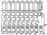
제1도는 본발명의 실시예에 따른 용장메모리 셀 블록을 가진 8비트출력 EPROM을 보여주는 전체적인 구성도이다. 제1도에 표시된 EPROM에서 메모리 셀 블록(11 내지 19)가운데에서 8비트의 출력단자(Q1 내지 Q8)에 대응하는 메모리 셀 블록(11 내지 18)은 각각 스위칭회로(21 내지 28)를 통하여 출력버퍼(31 내지 38)에 접속된다. 메모리 셀 블록(19)는 스위칭회로(29)를 통하여 스위칭회로(21 내지 28)에 접속된 용장메모리 셀 블록이며 이것은 출력단자(Q1 내지 Q8)중의 하나에 대응하는 고장메모리 셀 블록을 대체시킨다. 각 스위칭회로로(21 내지 29)의 스위칭은 제어신호 발생횔로(41 내지 19)로부터의 제어신호(BRi, 단 i=1,2,..., 또는 9)에 의해 제어된다. 각 제어신호 발생회로(41 내지 19)에서 제어신호(BRi)는 여기에 갖춰진(제1도에는 표시되어 있지 않으나 후에 제9도를 참고로 하여 상세히 설명됨)퓨우즈의 전도 또는 비전도상태에 따라서 출력된다. 메모리 셀 블록 (11 내지 18)중의 하나의 고장난 메모리 셀 블록을 용장 메모리 셀 블록(19)과 대체하기 위하여 대응하는 제어신호발생회로내의 퓨우즈가 대체될 메모리 셀 블록에 대응하는 퓨우즈 용단 신호(FC1 내지 FC8)중의 하나에 의해 용단 된다.1 is an overall configuration diagram showing an 8-bit output EPROM having a redundant memory cell block according to an embodiment of the present invention. In the EPROM shown in FIG. 1, the
또한 제어신호 발생회로(49)내의 퓨우즈 용장 메모리 셀 블록(19)에 대응하는 퓨우즈 용장신호(FC9)에 의해 용단된다. 퓨우즈 용단 신호(FC1 내지 FC8)는 대체신호(replacing Signal : RW)에 응하여 발생되며 각각 출력단자((Q1 내지 Q8)에 대체되는 블록선택신호가 가해진다.In addition, melting is performed by the fuse redundant signal FC9 corresponding to the fuse redundant
메모리 셀 블록(11 내지 19)은 또한 실리콘 기호로서 언급된 전자 시그니춰를 기억하기 위하여 각각 특정영역(11a,12a,13a,…, 및 19a)을 갖는다. 이 특정영역은 ROM으로 이루어진다. 각각 메모리 셀 블록(11 내지 19)의 나머지영역(11b,12b,…, 및 19b)은 EPROM이다. 일고장 메모리 셀 블록을 용장 메모리 셀블록(19)으로 대체함에 의해서 고장 메모리 셀 블록에 대하여 정확한 전자 시그니춰가 후에 상세히 설명될 용장 메모리 셀 블록(19)내의 특정영역(19a)으로부터 판독될 수 있다.The memory cell blocks 11 to 19 also have
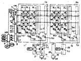
제2도에는 제1도에 표신된 EPROM에서 메모리 셀 블록(11), 용장 메모리 셀 블록(19) 및 스위칭회로(21 및 29)의 구성이 좀더 상세히 표시되어 있다. 메모리 셀 블록(11)에 있어서 복수의 워어드 라인(WL)과 복수의 비트라인(BL)이 직교하게 되어 있다. 워어드라인(WL)과 비트라인 사이의 각 교차 위치상에는 EPROM셀(MC)이 갖추어져 있다. 특정영영에는 워어드라인과 병렬로 뻗어있는 가상 워어드선 (Virtual word line : VWL)이 갖추어져 있다. 가상 워어드라인(VWL)과 각 비트라인(BL)사이에는 ROM 셀(RC) 접속된다. ROM 셀(RC)은 각 비트라인(BL)에 그들을 접속 또는 비접속시킴에 의해서 전자 시그니춰 데이타를 기억하도록 채용된다. 전자 시그니춰의 예는 제4도 및 제5도를 참고하여 후에 설명될 것이다. 가상 워어드라인(VWL)은 어드레스 입력 단자(A9)에 가해진 가상워어드라인 선택신호를 검출하여 ROM셀(RC)로부터 전자기호를 판독하기 위한 가상워어드라인(VWL)을 구동하는 신호검출회로(5)에 접속된다. 각 워어드라인(WL)은 행(row)디코우더 회로(6)에 접속된다. 그리고 가상 워어드라인(VWL)상에 신호가 " H "로 될때 행 디코우더(6)는 이 신호에 의해 제어되어 모든 워어드라인이 " L " 이 되게 한다.FIG. 2 shows the configuration of the
메모리 셀 블록(11)은 각각이 16비트라인(BL)을 포함하고 있는 8서브블록(11-0,11-1,…, 및 11-7)으로 분할되어 있다. 제1서브블록(11-0)내의 16비트라인(BL)모두는 각각 비트라인 선택 트랜지스터(Ta0, Ta1, …, 및 Ta15), 서브 블록 선택 트랜지스터( Tb0) 및 스위칭회로(21)내의 메모리 셀 블록 선택 트랜지스터( Tc1)를 통하여 동일한 출력버퍼(31)에 접속된다.The
또한 스위칭회로(21)는 제어신호발생회로(41)로부터 제어신호(BR1) 를 받아들이기위한 입력과 트랜지스터( Tc1)의 게이트에 접속된 출력을 가지고 있는 인버어터(IV1) 를 포함하고 있다. 또한 스위칭회로(21)는 인버어터(IV1) 의 입력에 접속된 게이트를 가지고 있는 용장블록 선택 트랜지스터( Tc2)를 포함한다. 트랜지스터(Tc1및 Tc2)의 소오스는 출력버퍼(31)에 접속된다.The switching
기타 메모리 셀 블록 각각은(12,13,…, 및 19) 메모리 셀 블록(11)과 동일한 회로 구성을 가지고 있다.Each of the other memory cell blocks (12, 13, ..., and 19) has the same circuit configuration as the
각각 메모리 셀 블록 (12,13,…, 및 18)에 대응하는 각 스위칭회로(22,23,…, 및 28)는 스위칭회로(21)과 동일한 회로 구성을 가지고 있다. 반대로 용장 메모리 셀 블록(19)에 대응하는 스위칭회로는 제어신호(BR9) 를 받아들이도록 채택된 게이트 전극을 가진 단일 스위칭 트랜지스터(Tc3)를 가지고 있다. 용장 메모리 셀 블록(19)내의 서브블록 선택 트랜지스터( Tb0, Tb1, …, 및 Tb7)의 소오스는 스위칭 트랜지스터(Tc3)를 통하여 모든 스위칭회로(21 내지 28)내의 용장블록 선택 트랜지스터(Tc2)의 드레인에 공통으로 접속된다.Each of the switching
모든 메모리 셀 블록(11 내지 19)내의 각 서브블록에서 비트라인선택트랜지스터(Ta0, Ta1, …, 및 Ta15)의 게이트 전극은 각각 비트라인 선택신호(BO,B1,…, 및 B15)를 받아들이도록 사용된다. 비트라인 선택신호(BO,B1,…, 및 B15)는 낮은 차수의 열 어드레스 입력신호(A0,A1,A2 및 3)를 해독하는 제1열 해독기회로(7)로부터 공급되어 비트라인 선택신호(BO,B1,…, 및 B15)중의 하나를 고전위레벨 " H "로 되게 한다.The gate electrodes of the bit line select transistors T a0 , T a1 ,..., And T a15 in each subblock in all the memory cell blocks 11 to 19 are respectively the bit line select signals BO, B1, ..., and B15. It is used to accept. The bit line selection signals BO, B1, ..., and B15 are supplied from the first
각 메모리 셀 블록(11 내지 19)에서 서브블록 선택 트랜지스터( Tb0, Tb1, …, 및 Tb7)의 게이트 전극은 각각 서브블록 선택신호(C0, C1, …, 및 C7)를 받아들이도록 사용된다. 서브블록 선택신호(C0, C1,…, 및 C7)는 높은 차수의 열 어드레스신호(a4, a5 및 a6)를 해독하는 제 2 열 해독기회로(8)로부터 공급되어 서브 블록선택신호(C0, C1,…, 및 C7)중 하나를 고전위레벨 " H "이 되게 한다. 따라서, 열 어드레스 신호(A0 내지 A3 및 a4 내지 a6)를 지정함에 의해서 각 메모리 셀 블록내의 8서브블록중 하나가 선택되고 선택된 서브블록 각각의 16 비트 라인(BL) 중의 하나가 선택된다.In each of the memory cell blocks 11 to 19, the gate electrodes of the subblock selection transistors Tb0 , Tb1 , ..., and Tb7 are used to receive the subblock selection signals C0, C1, ..., and C7, respectively. do. The subblock selection signals C0, C1, ..., and C7 are supplied from the second
또한 가상 워어드라인(VWL)은 행 디코우더회로(6) 및 어드레스 신호 발생회로(9)에 접속된다. 가상 워어드라인(VWL)이 선택될때 기준전압(VRR)이 행 디코우더회로(6) 에 인가되어 그것의 동작을 금지시키며 그리고 제어신호(BR1 내지 BR9)에 응하여 고정된 세트의 어드레스신호(a4, a5 및 a6)를 발생하도록 어드레스 신호 발생회로(9)에 인가된다.The virtual word line VWL is also connected to the
이 실시예에서 용장 메모리 셀 블록(19)을 제외한 1메모리 셀 블록내의 모든 ROM셀(RC)은 제3도에 표시된 바와같이 동일 데이타를 기억한다. 즉, 제3도에서 제1도 및 제2도에 사용된 동일한 참조부호는 동일부품을 나타낸다. 참조기호(D1, D2,…,D8)는 제2도에 표시된 메모리 셀 블록(11 내지 19)에 기억된 전자 시그니춰 데이타를 나타낸다. 참조기호(M11,M12,…,M18,M21,M22,…,M28,…,M91,M92, 및 M98)는 제2도에 표시된 각 서브블록(11-0,11-1,…,11-7,12-0,…,12-7,19-0,…, 및 19-7)의 메모리 셀(MC)내에 기억된 데이타를 표시한다. 제3도에 표시된 바와같이 메모리 셀 블록(11)내의 모든 서브 블록은 동일한 데이타(D1)을 기억한다. 또한 메모리 셀 블록(12)내의 모든 서브 블록은 동일한 데이타(D2) 를 기억한다. 마찬가지로 각 메모리 셀 블록(13 내지 18)내의 모든 서브 블록은 각각 동일한 데이타(D3,D4,…, 또는 D8)를 기억한다. 반대로 용장메모리 셀 블록(19)에 있어서 각 서브 블록(19-0, 19-1,..., 및 19-7)은 각각 메모리 셀블록(11 내지 18)에 기억된 데이타를 대응하는 데이타(D1,D2,…, 및 D8)를 기억한다.In this embodiment, all the ROM cells RC in the one memory cell block except the redundant
이제 제2도에 표시된 회로의 동작을 설명한다.The operation of the circuit shown in FIG. 2 will now be described.
전자 시그니춰가 판독되어야 하고 메모리 셀 블록(11 내지 18)중 하나가 오동작중일때 가상 워어드라인(VWL)은 12V의 어드레스 입력신호(또한 참조기호(AP)로 표시됨)를 신호 검출회로에 인가함에 의해서 선택되며 모든 워어드라인(WL)은 행 디코우더 회로(6)가 금지되어 선택된 가상 워어드라인(VWL)에 의해 동작되기 때문에 선택되지 않는다. 선택된 가상 워어드라인(VWL)은 기준전압(VRR)을 어드레스 신호 발생회로 (9)에 공급한다. 따라서 용장 메모리 셀 블록(19)에 오동작 또는 고장메모리 셀 블록 대신에 사용된다. 메모리 셀 블록(11)이 오동작중이라고 가정한다. 제어신호(BR1 및 BR9)는 그후 " H " 레벨로 된다. 제어신호 (BR1)의 " H " 레벨은 인버어터(IV1)에 의해 반전되어 그결과 메모리 셀 블록 선택 트랜지스터(TC1)는 차단상태로 된다. 반면에 " H " 레벨은 제어신호 (BR1)는 용장 블록 선택 트랜지스터(Tc2)의 게이트에 직접 인가되어 트랜지스터(Tc2)는 동작상태가 된다. 또한 스위칭 회로(29)내의 전달 게이트 트랜지스터(Tc3)는 제어신호(BR9)에 의해 동작상태로 된다. 오동작 메모리 셀 블록(11)내에 기억된 전자 시그니춰 데이터가 판독되어야 할때 어드레스 입력신호(A4 내지 A6)에 관계없이 " H " 레벨로 서브블록 선택신호(CO)를 고정시키는 것은 충분하다. 이와 같은 서브블록 선택신호(CO)의 동작을 고정시키는 것은 뒤에 상세히 설명될 어드레스 신호 발생회로(9)에 의해 수행된다. 따라서 오동작 메모리 셀 블록(11)에 기억된 데이터(D1)대신에 용장 메모리 셀 블록(19)의 제1서브블록(19-0)에 기억된 데이타(D1)는 트랜지스터(Tc3, 및 Tc2)를 통하여 출력버퍼(31)에 전달된다.When the electronic signature is to be read and one of the memory cell blocks 11 to 18 is malfunctioning, the virtual word line VWL applies a 12V address input signal (also denoted by reference symbol AP) to the signal detection circuit. All the wordlines WL are not selected because the
제2도에 표시된 EPROM이 전자 시그니춰를 판독하지 않고 그리고 고장 메모리 셀 블록을 용장 메모리 셀 블록(19)으로 대체하지 않고 통상의 EPROM으로 사용될때 모든 제어신호(BR1 내지 BR9)는 저 전위레벨 " L" 로 세트되며 어드레스 입력단자(A9)의 어드레스 입력신호(A9), 즉 가상워어드라인 선택신호는 12V의 고전위로 상승되지 않는다. 결과적으로 모든 스위칭회로(21 내지 28)내의 비트라인 선택신호(Tc1)는 도전성이되며 스위칭회로(29)내의 전달 게이트 트랜지스터(Tc3)는 비도전성이 된다. 또한 행 디코우더회로(6)는 행 어드레스신호(A7,A8,…, 및 A17)를 해독하여 워어드라인(WL)중 하나를 고전위레벨 " H " 로 되게 하며 가상 워어드라인(VWL)은 선택되지 않는다. 따라서 EPROM셀(MC)은 그로부터 데이타를 판독하거나 거기에 데이타를 기입하거나 이들 메모리 셀 (MC)내의 데이타를 소거하도록 선택된다.When the EPROM shown in FIG. 2 is used as a normal EPROM without reading the electronic signature and replacing the failed memory cell block with the redundant
고장 메모리 셀 블록, 예를 들면 메모리 셀 블록(11)이 메모리 셀 (MC)의 억세싱동안 용장 메모리 셀 블록(19)에 의해 대체될때 대체동작은 전자 시그니춰가 판독되어질때와 사용된것과 동일하다. 이경우에 가상 워어드라인(VWL)은 선택되지 않는다.When the failed memory cell block, e.g.,
임의의 다른 고장 메모리 셀 블록을 용장 메모리 셀 블록(19)으로의 대체는 고준위레벨 " H " 로 대응하는 제어신호(BRi, i=2,3,…, 또는 8) 및 제어신호(BR9)를 선택함에 의해서 수행될 수 있다.Substitution of any other failed memory cell block with redundant
제4도는 JEDEC에 의해 제안된 전자 시그니춰의 형식을 보여주는 테이블이다. 제4도는 표시된 바와같이 16전자 시크니춰(ES1,ES2,…, 및 ES16)는 제2도에 표시된 EPROM의 ROM셀(RC)에 기억된다. 각 실리콘 기호, 즉 전자 시그니춰는 8비트 데이타로 이루어져 있다. 1전자 시그니춰 내의 각 비트는 8출력단자(Q1 내지 Q8)중 하나로 부터 출력된다. 제1전자 시크니춰(ES1)는 8비트 데이타(d10,d20,…, 및 d80)로 구성된 제조업자의 코우드(M.C)이다. 제2전자 시크니춰(ES2)는 8비트 데이타(d11,d21,…, 및 d81)로 구성된 프로그래밍 알고리즘 코우드(A.C)이다. 제3전자 시크니춰(ES3) 내지 제16전자 시크니춰(ES16)는 각 제조업자에게 개별적으로 한정된다. 제2도에 표시된 회로에서 제1전자 시크니춰의 8비트 데이타(d10,d20,…, 및 d8)는 각각 메모리 셀 블록(11 내지 18)에 기억된다. 좀더 엄밀하게 말하면 최하위 비트 데이카는 제 1 메모리 셀 블록(11)의 각 서브 블록내에서 비트라인 선택신호(BO)에 의해 선택되는 제 1 비트라인(BL)과 협력하여 제1ROM 셀(RC)에 기억된다. 마찬가지로 나머지 비트 데이타 (d30,d40,..., 및 d80)는 각각 각 메모리 셀 블록(13 내지 18)내의 비트라인 선택기호(BO)에 의해 선택된 제 1ROM 셀(RC)에 기억된다.4 is a table showing the format of the electronic signature proposed by JEDEC. As shown in FIG. 4, the 16 electronic signatures ES1, ES2, ..., and ES16 are stored in the ROM cell RC of the EPROM shown in FIG. Each silicon symbol, or electronic signature, consists of 8-bit data. Each bit in one electronic signature is output from one of the eight output terminals Q1 to Q8. The first electronic signature ES1 is the manufacturer's code MC consisting of 8-bit data d 10 , d 20 ,..., And d 80 . The second electronic signature ES2 is a programming algorithm code AC consisting of 8 bit data d 11 , d 21 ,..., And d 81 . The third electronic signature ES3 to the sixteenth electronic signature ES16 are individually limited to each manufacturer. In the circuit shown in FIG. 2, 8-bit data d 10 , d 20 ,..., And d 8 of the first electronic signature are stored in the memory cell blocks 11 to 18, respectively. More precisely, the least significant bit data is the first ROM cell RC in cooperation with the first bit line BL selected by the bit line selection signal BO in each sub block of the first
제2전자시그니춰(ES2)의 8비트 데이타(d11,d21,…4, 및 d81)는 각각 메모리 셀 블록(11 내지 18)내의 비트라인 선택신호(B1)에 의해 선택된 제2 ROM 셀(RC)에 기억된다.The 8-bit data d 11 , d 21 ,... 4, and d 81 of the second electronic signature ES2 are respectively selected by the second ROM cell selected by the bit line selection signal B1 in the memory cell blocks 11 to 18. (RC) is remembered.
따라서 각 전자 시그니춰의 8비트 데이타는 각 메모리 셀 블록(11 내지 18)내의 각 ROM 셀에 기억된다. 따라서 제1메모리 셀 블록(11)내의 각 서브블록(11-0 내지 11-7)은 사선으로 제4도에 표시한 바와같은 16비트 데이타 (d10,d11,…, 및 d116)로 구성되는 데이타(D1)를 기억한다. 각 서브블록(12-0 내지 12-7)은 16비트(d20,d21,…, 및 d215)로 구성되는 데이타(D2)를 기억한다. 마찬가지로 나머지 메모리 셀 블록(13 내지 18) 각각은 8세트의 동일한 16비트 데이타(D3,D4,…, 및 D8)을 기억한다.Therefore, 8-bit data of each electronic signature is stored in each ROM cell in each
제4도에 표시된 테이블에서 별표 표시가 있는 출력단자(Q8) 로 부터 출력된 최상위 비트 데이타(d80,d81,…, 및 d816)는 각 전자 시그니춰에 대한 기수패리티 비트이다.The most significant bit data (d 80 , d 81 ,..., And d 816 ) output from the output terminal Q 8 with an asterisk in the table shown in FIG. 4 is the odd parity bit for each electronic signature.
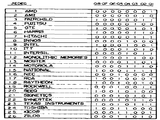
제5도는 제1전자 시그니춰(ES2) 즉 제조업자 코우드의 여러가지 예를 보여주는 테이블이다. 제5도에서 예를 들어 AMD에 대한 제조업자 코우드는 8비트 데이타(OOO OO O1)로 이루어져 있다. 각 비트는 출력단자(Q1 내지 Q8)중의 하나로부터 출력된다. 이 제조업자 코우드는 각 장치의 ROM 셀(RC)에 기억되어서 사용자가 장치를 식별할 수 있도록 한다.5 is a table showing various examples of the first electronic signature (ES2), that is, the manufacturer code. In Figure 5, for example, the manufacturer code for AMD consists of 8-bit data (OO OO O1). Each bit is output from one of the output terminals Q1 to Q8. The manufacturer code is stored in the ROM cell (RC) of each device to allow the user to identify the device.
제6도는 고차 열 어드레스 신호(a4, a5 및 a6)와 선택된 서브블록사이의 관계를 표시하는 테이블이다. 제6도에서 행 어드레스 신호(a4, a5 및 a6)가 각각 0,0,0일때 서브블록 선택신호(CO)는 "H"레벨로 선택되어 그결과 대응 서브블록(11-0, 12-0,…, 및 19-0) (제2도)이 선택된다. 이 경우에 메모리 셀 블록(11)은 용장 메모리 셀 블록(19)에 의해 대체될 수 있다. 또한 행 어드레스 신호(a4, a5 및 a6)가 각각 1,0,0일때 서브블록 선택신호(C1)는 " H " 레벨로 선택되어 대응하는 서브블록(11-1, 12-1,…, 및 19-1)이 선택된다. 이 경우에 메모리 셀 블록(12)은 용장 메모리 셀 블록(19)에 의해 대체될 수 있다. 행어드레스 신호(a4, a5 및 a6)의 다른 조합들은 "H"레벨인 대응하는 서브블록 선택신호(C2,C3,…, 및 C7)를 발생한다. 행어드레스 신호(a4, a5, 및 a6)의 조합을 소망하는 세트로 고정시킴에 의해서 소망하는 서브 블록 선택 신호가 선택된다. 결과적으로 대체동작이 수행된다.6 is a table indicating the relationship between the higher order column address signals a4, a5 and a6 and the selected subblock. In FIG. 6, when the row address signals a4, a5, and a6 are 0, 0, and 0, respectively, the subblock selection signal CO is selected to the "H" level, and as a result, the corresponding subblocks 11-0 and 12-0. , ..., and 19-0) (Figure 2). In this case, the
제7도는 어드레스 신호 발생회로(9)를 좀더 상세히 설명하는 회로도이다. 제7도에서 어드레스 신호 발생회로(9)는 3개 어드레스 신호 선택회로(S1,S2, 및 S3) 및 9개 어드레스 신호 결정회로(AD1,AD2,…, 및 AD9)로 구성되어 있다. 각 어드레스 신호 선택회로(S1,S2, 및 S3)는 상보형 금속산화 반도체(complementary metal oxide semiconductor : CMOS)트랜지스터로 이루어진 2개의 인버어터(I1 및 I2), 2개의 전달게이트(TG1 및 TG2) 및 2개의 CMOS 인버어터(I3 및 I4)를 포함하고 있다. 이 인버어터들(I1 내지 I4)은 파형 형성회로로 작용을 한다. 각 전달 게이트(TG1 및 TG2)는 병렬로 접속된 P 채널 MOS 트랜지스터 및 N 채널 MOS 트랜지스터로 이루어져 있다. 각 어드레스 신호 판별회로(AD1 내지 AD9)는 3개의 전달게이트(TG3, TG4 및 TG5)를 포함한다. 각 전달 게이트(TG3, TG4 및 TG5)를 병렬로 접속된 P 채널 MOS트랜지스터 및 N 채널 MOS 트랜지스터로 이루어져 있다. 대체동작이 이루어져야 할때 어드레스신호 결정회로(AD1 내지 AD8)는 각각 서브블록 선택신호(C0, C1,…, 및 C7)를 선택하기 위한 어드레스 신호(a4,a5, 및 a6)세트를 결정한다. 즉, 대체동작이 발생할때 각 회로(AD1 내지 AD8)에서 전달게이트(TG3)는 어드레스 신호(a4)를 결정하고 ; 전달게이트(TG4)는 어드레스 신호(a5)를 결정하며 ; 전달 게이트(TG5)는 어드레스 신호(a6)를 결정한다. 결국 어드레스신호 결정회로(AD1)에서 전달게이트(TG3,TG4 및 TG5)의 모든 입력은 저항(R)을 통하여 접지되어 그결과 회로(AD1)는 어드레스 신호(a4,a5,a6)세트가 (0,0,0)와 동일하게 되도록 결정할 수 있다. 또한 어드레스 신호 결정 회로(AD2)에서는 전달게이트( TG3)의 입력은 저항(R)을 통하여 전원(Vcc)에 접속되며 전달게이트(TG4 및 TG5)의 기타 2입력은 저항(R)을 통하여 접지되므로 회로(AD2)는 어드레스 신호(a4,a5,a6)세트가 (1,0,0)와 동일하게 되도록 결정할 수 있다. 마찬가지로 다른 어드레스 신호 결정 회로(AD3 내지 AD8)에서도 전달게이트(TG3, TG4 및 TG5)의 입력은 소망하는 어드레스 신호(a4,a5 및 a6)세트에 따라서 저항(R)을 통하여 전원(Vcc)또는 접지에 연결된다.7 is a circuit diagram illustrating the address
제7도에 표시된 회로의 동작에 의해서 대체동작이 수행되지 않을때 가상 워어드 라인(VWL)이 선택되지 않으므로(제2도 참조) 기준전압(VRR)은 저 레벨 "L"이 된다. 기준전압(VRR)이 전달게이트(TG1)의 P채널 MOS 트랜지스터의 게이트 및 전달게이트(TG2)의 N 채널 MOS 트랜지스터의 게이트에 인가된다. 반전된 기준전압(![]()
![]()
메모리 셀 블록(11)이 용장메모리 셀 블록(19)으로 대체될때 제어신호(BR1 및 BR9)는 " H "는 레벨로 선택된다. 제어신호(BR1)는 제1어드레스 신호 결정회로(AD1)내의 전달게이트(TG3,TG4 및 TG5)의 N 채널 MOS 트랜지스터의 게이트에 인가된다. 반전제어신호(![]()
![]()
![]()
![]()
회로(AD1)내의 전달게이트(TG3)의 입력은 저항(R)을 통하여 접지되므로 그 출력은 " 0 " , 즉 " L "레벨로 된다. 마찬가지로 전달게이트(TG4 및 TG5)의 출력은 " L "레벨로 된다.Since the input of the transfer gate TG3 in the circuit AD1 is grounded through the resistor R, its output is at " 0 " Similarly, the outputs of the transfer gates TG4 and TG5 are at the "L" level.
따라서 제2열 디코우더(8)는 외부어드레스 입력신호(A4,A5 및 A6)에 관계없이 각각 0,0,0와 같은 어드레스 신호(a4,a5,a6)을 받아들인다. 어드레스신호(0,0,0)에 응하여 제2열 디코우더(8)는 제1서브블록 선택신호(CO)를 선택한다.Therefore, the
마찬가지로 제어신호(BR2)가 " H "레벨로 선택될 때 제2열 디코우더(8)는 외부어드레스 입력신호(A4,A5 및 A6)에 관계없이 제2서브블록신호(C1)를 선택한다.Similarly, when the control signal BR2 is selected to the "H" level, the
제어신호(BR3,BR4,…, 또는 BR8)가 선택될때 서브블록 선택신호(C3,C4,…, 또는 C8)가 각각 선택된다.When the control signals BR3, BR4, ..., or BR8 are selected, the subblock selection signals C3, C4, ..., or C8 are selected, respectively.
제8도는 신호검출회로(5)를 좀더 상세하게 보여주는 회로도이다. 제8도에서 신호검출회로(5)는 P채널 MOS트랜지스터(Q1), N채널 MOS트랜지스터(Q2) 및 인버어터(IV)를 포함한다.8 is a circuit diagram showing the
트랜지스터(Q1)의 게이트는 접지된다.The gate of transistor Q1 is grounded.
트랜지스터(Q1)의 소오스는 전원 Vcc에 연결된다. 트랜지스터(Q1)의 드레인은 트랜지스터(Q2)의 드레인에 접속된다. 트랜지스터(Q2)의 소오스는 접지된다.The source of transistor Q1 is connected to power supply Vcc. The drain of the transistor Q1 is connected to the drain of the transistor Q2. The source of transistor Q2 is grounded.
트랜지스터(Q1)와 트랜지스터(Q2)사이의 접속점은 인버어터(IV)의 입력에 접속된다. 트랜지스터(Q2)는 12V보다 조금낮은 높은 드레시호울드 전압, 예를 들어 10V의 전압을 갖는다.The connection point between transistor Q1 and transistor Q2 is connected to the input of inverter IV. Transistor Q2 has a high threshold voltage, slightly less than 12V, for example a voltage of 10V.
트랜지스터 (Q2)의 게이트는 어드레스 입력단자(A9)에 접속된다. 12V의 고전압이 어드레스 입력단자(A9)에 인가될때 트랜지스터(Q2)는 동작상태로 되어 인버어터(IV)의 출력은 고레벨" H "의 기준전압(VRR)을 제공한다. 반전 기준전압(![]()
![]()
기준전압(VRR)은 가상워어드라인(VWL), 회로(S1,S2 및 S3)(제7도)내의 전달게이트 및 동작을 금지시키기 위한 행 디코우더 회로(6)(제2도)에 가해진다.The reference voltage VRR is applied to the row decoder circuit 6 (FIG. 2) for prohibiting the transfer gate and operation in the virtual word line VWL, the circuits S1, S2 and S3 (FIG. 7). Is applied.
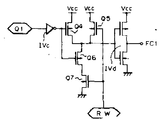
제9도는 제어신호 발생회로(41)를 좀더 상세히 보여주는 회로도이다. 제9도에서 제어신호 발생회로(41)는 퓨우즈(F1), N채널 MOS 트랜지스터(Q3), 저항(R) 및 2인버어터(IVa 및 IVb)를 포함한다.9 is a circuit diagram showing the control
퓨우즈(F1)는 전원(Vcc)과 트랜지스터(Q3)의 드레인 사이에 접속된다. 트랜지스터(Q3)의 소오스는 접지된다. 저항(R)은 트랜지스터(Q3)의 드레인과 접지사이에 접속된다. 트랜지스터(Q3)의 드레인은 제1단 인버어터(IVa)의 입력에 접속된다.The fuse F1 is connected between the power supply Vcc and the drain of the transistor Q3. The source of transistor Q3 is grounded. Resistor R is connected between the drain of transistor Q3 and ground. The drain of the transistor Q3 is connected to the input of the first stage inverter IVa.
제 1단 인버어터(IVa)의 출력은 제2단 인버어터(IVb)의 입력에 접속된다. 퓨우즈용단 신호(FC1)가 트랜지스터(Q3)의 게이트에 인가될때 트랜지스터(Q3)는 동작상태로 되어 퓨우즈(F1)를 통하여 전류가 흘러서 퓨우즈(F1)를 용단시킨다. 그후 트랜지스터(Q3)의 드레인은 " L " 레벨로 전환된다. 결과적으로 제어 신호(BR1)는 제1단 인버어터(IVa)의 출력에서 얻어진다. 또한 반전제어신호(![]()
![]()
![]()
![]()
기타 제어신호 발생회로(42 내지 49)는 제9도에 표시된 것과 동일한 회로구성을 갖는다.The other control
제10도는 퓨우즈용단신호(FC1)를 발생하기 위한 회로를 보여주는 회로도이다.10 is a circuit diagram showing a circuit for generating the fuse short signal FC1.
제10도에서 회로는 입력단 인버어터(IVc), 2개의 P채널 MOS트랜지스터(Q4, Q5), 2개의 N채널 MOS트랜지스터(Q6, Q7) 및 출력단 인버어터(IVd)를 포함하고 있다.In FIG. 10, the circuit includes an input stage inverter IVc, two P-channel MOS transistors Q4 and Q5, two N-channel MOS transistors Q6 and Q7, and an output stage inverter IV d .
인버어터(IVc)의 출력은 트랜지스터(Q4 및 Q6)의 게이트에 접속된다.The output of inverter IVc is connected to the gates of transistors Q4 and Q6.
트랜지스터(Q4 및 Q6)의 소오스는 전원(Vcc)에 접속된다. 트랜지스터(Q4, 및 Q5)의 드레인은 트랜지스터(Q6)의 소오스 및 인버어터(IVd)의 입력에 접속된다. 트랜지스터( Q6)의 드레인은 트랜지스터( Q7)의 드레인에 접속된다.The sources of transistors Q4 and Q6 are connected to a power supply Vcc. The drains of the transistors Q4 and Q5 are connected to the source of the transistor Q6 and the input of the inverter IV d . The drain of the transistor Q6 is connected to the drain of the transistor Q7.
트랜지스터( Q7)의 소오스는 접지된다.The source of transistor Q7 is grounded.
대체신호(RW)가 " L " 레벨로 될때 P채널 트랜지스터( Q5)는 도전성으로 되며 N채널 트랜지스터(Q7)는 비도전성으로되어 인버어터(IVd)의 입력은 " H " 레벨로 된다. 이 경우에 퓨우즈 용단 신호(FC1)는 " L " 레벨로 되어 퓨우즈(F1) (제9도)는 용단되지 않는다.When the replacement signal RW becomes "L" level, the P-channel transistor Q5 becomes conductive and the N-channel transistor Q7 becomes non-conductive, so that the input of the inverter IV d becomes "H" level. In this case, the fuse melting signal FC1 is at the "L" level, and the fuse F1 (FIG. 9) is not melted.
단자(Q1)가 " L " 레벨이고 대체신호(RW)가 " H " 레벨일때 트랜지스터(Q4 및 Q5)는 차단상태로 되며 트랜지스터(Q6및 Q7)는 동작상태로 되어 인버어터(IVd)의 입력은 " L " 레벨로 된다. 이경우에 퓨우즈용단신호(FC1)는 " H " 레벨로 되어 퓨우즈(F1) (제9도)를 용단시킨다.When the terminal Q1 is at the "L" level and the replacement signal RW is at the "H" level, the transistors Q4 and Q5 are turned off, and the transistors Q6 and Q7 are turned on to operate the inverter IV d. The input is at the "L" level. In this case, the fuse short signal FC1 becomes "H" level to melt the fuse F1 (FIG. 9).
퓨우즈용단신호(FC2 내지 FC8) 발생회로는 제10도에 표시된 회로와 동일한 회로구성을 가지고 있다.The fuse short signal FC2 to FC8 generation circuit has the same circuit configuration as the circuit shown in FIG.
명백한 바와같이 출력단자(Q1 내지 Q8)는 판독데이타를 출력하거나 또는 기입데이타를 입력시키는것뿐 아니라 대체 블록 선택신호를 가하는데에 사용된다.As is apparent, the output terminals Q1 to Q8 are used for outputting read data or inputting write data as well as for applying a replacement block selection signal.
제11도는 용장 서브블록에 대응하는 퓨우즈용단신호(FC9)를 발생하기 위한 회로를 보여주는 회로도이다.11 is a circuit diagram showing a circuit for generating the fuse short signal FC9 corresponding to the redundant subblock.
제9도에서 회로는 2개의 인버어터(IVe 및 IVf)로 이루어져 있다. 대체 신호(RW)가 " H " 레벨일때 퓨우즈용단신호(RC9)는 " H " 레벨로 전환되어 퓨우즈(F9)(표시안됨)를 용단시킨다.In FIG. 9, the circuit consists of two inverters IVe and IV f . When the replacement signal RW is at the "H" level, the fuse short signal RC9 is switched to the "H" level to melt the fuse F9 (not shown).
상기한 실시예에서 각 메모리 셀블록(11 내지 18)은 8세트의 동일한 16비트데이타(D1,D2,…, 또는 D8)를 기억한다. 예를들면 메모리셀블록(11)은 제3도에 표시한 바와같이 특정영역(11a)에 8세트의 16비트데이타(D1)를 기억한다. 그러나 본 발명은 상기 설명한 실시예에 제한되지 않는다.In the above embodiment, each
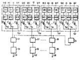
제12도는 본 발명의 다른 실시예에 따른 EPROM을 보여주는 블록회로도이다. 제12도에서 제3도에 사용된 것과 동일한 참조기호는 동일한 부품을 표시한다.12 is a block circuit diagram illustrating an EPROM according to another embodiment of the present invention. The same reference numerals as used in FIG. 12 to FIG. 3 denote the same parts.
제3도와 제12도와의 중요한 차이점은 메모리셀블록(11a,12a,…, 및 18a)에 있다. 즉, 제12도에서는 각 메모리 셀블록(11a,12a,......, 및 18a)은 각각 제1서브블록(11a-O, 12a-O, 13a-O, 또는 18a-O)내에 8세트 대신에 단일세트의 16비트 데이타(D1,D2,…, 또는 D8)를 포함한다.An important difference between FIG. 3 and FIG. 12 lies in the
또한 부가적인 서브블록 선택 트랜지스트(Qa)가 메모리 셀 블록(11a 내지 18a)중 하나내의 서브블록 선택 트랜지스터(Tbo)와 병렬로 접속된다.An additional subblock select transistor Qa is also connected in parallel with the subblock select transistor Tbo in one of the
부가 서브블록 선택트랜지스터(Qa)의 게이트는 가상 워어드선( VWL)에 접속된다.The gate of the additional subblock select transistor Qa is connected to the virtual word line VWL.
제13도는 제12도에 표시된 EPROM내의 메모리 셀 블록(11a)을 좀더 상세히 보여주는 회로도이다.FIG. 13 is a circuit diagram showing in more detail the
제13도에서 ROM 셀 (RC)은 단지 제1서브블록(11a-O)내에만 갖춰진다. 또한 부가 서브블록 선택 트랜지스터(Qa)는 트랜지스터(Tbo)에 병렬로 접속된다.In FIG. 13, the ROM cell RC is provided only in the
제12도 및 제13도에 표시된 구성에 의해 용장 메모리 셀 블록(19)이 전자 시그니춰를 판독하는 동안 사용되지 않았을때 가상되어 드라인(VWL)은 " H " 레벨로 선택되어 데이타(D1,D2,…, 및 D8)는 각각 서브블록(11a-O, 12a-O, …, 및 18a-O)으로 부터 판독된다.12 and 13, the redundant
용장 메모리 셀 블록(19)이 전자 시그니춰를 판독하는 동안 사용될때 제7도에 표시된 회로는 또한 앞에서 언급한 실시예에서와 동일한 방법으로 사용된다.When the redundant
전술한 설명으로부터 명백한 바와같이 본발명에 따르면 용장구성을 가진 반도체 기억장치에 있어서 임의의 출력 비트에 대응하는 메모리 셀 블록이 용장 메모리 셀 블록에 의해 대체될때 조차도 전자 시그니춰를 정확하게 판독할 수 있는 전자 시그니춰 판독회로가 제공될 수 있다.As is apparent from the foregoing description, according to the present invention, in a semiconductor memory device having a redundant configuration, an electronic signature capable of accurately reading an electronic signature even when a memory cell block corresponding to an arbitrary output bit is replaced by the redundant memory cell block. A readout circuit can be provided.
본 발명은 언급된 실시예에 제한되는 것은 아니다.The invention is not limited to the examples mentioned.
본 발명의 정신을 벗어나지 않고 여러가지의 변경 및 수정이 가능하다. 예를들면 메모리 크기는 임으로 선택될 수 있다. 또한 본 발명은 EPROM 뿐 아니라 PROM 또는 RAM에도 적용할 수 있다.Various changes and modifications are possible without departing from the spirit of the invention. For example, the memory size may be randomly selected. In addition, the present invention can be applied not only to EPROM but also to PROM or RAM.
Claims (12)
Applications Claiming Priority (2)
| Application Number | Priority Date | Filing Date | Title |
|---|---|---|---|
| JP58018027A JPS59144098A (en) | 1983-02-08 | 1983-02-08 | Semiconductor memory |
| JP58-018027 | 1983-02-08 |
Publications (2)
| Publication Number | Publication Date |
|---|---|
| KR840008073A KR840008073A (en) | 1984-12-12 |
| KR890005156B1 true KR890005156B1 (en) | 1989-12-14 |
Family
ID=11960179
Family Applications (1)
| Application Number | Title | Priority Date | Filing Date |
|---|---|---|---|
| KR1019840000580A KR890005156B1 (en) | 1983-02-08 | 1984-02-08 | The semiconductor memory device |
Country Status (7)
| Country | Link |
|---|---|
| US (1) | US4604730A (en) |
| EP (1) | EP0116464B1 (en) |
| JP (1) | JPS59144098A (en) |
| KR (1) | KR890005156B1 (en) |
| CA (1) | CA1214553A (en) |
| DE (1) | DE3484514D1 (en) |
| IE (1) | IE56815B1 (en) |
Families Citing this family (28)
| Publication number | Priority date | Publication date | Assignee | Title |
|---|---|---|---|---|
| JPS6148200A (en) * | 1984-08-14 | 1986-03-08 | Fujitsu Ltd | Semiconductor memory device |
| JPS6355799A (en) * | 1986-08-26 | 1988-03-10 | Mitsubishi Electric Corp | Semiconductor memory device |
| JP2590897B2 (en) * | 1987-07-20 | 1997-03-12 | 日本電気株式会社 | Semiconductor memory |
| US4807191A (en) * | 1988-01-04 | 1989-02-21 | Motorola, Inc. | Redundancy for a block-architecture memory |
| JPH01167760U (en) * | 1988-05-16 | 1989-11-27 | ||
| US5134584A (en) * | 1988-07-22 | 1992-07-28 | Vtc Incorporated | Reconfigurable memory |
| JPH0289299A (en) * | 1988-09-27 | 1990-03-29 | Nec Corp | Semiconductor storage device |
| DE69033438T2 (en) | 1989-04-13 | 2000-07-06 | Sandisk Corp | Exchange of faulty memory cells of an EEprom matrix |
| US7190617B1 (en) | 1989-04-13 | 2007-03-13 | Sandisk Corporation | Flash EEprom system |
| US7447069B1 (en) | 1989-04-13 | 2008-11-04 | Sandisk Corporation | Flash EEprom system |
| KR910005601B1 (en) * | 1989-05-24 | 1991-07-31 | 삼성전자주식회사 | Semiconductor memory device having redundunt block |
| JP2837433B2 (en) * | 1989-06-05 | 1998-12-16 | 三菱電機株式会社 | Bad bit relief circuit in semiconductor memory device |
| JPH03116498A (en) * | 1989-09-28 | 1991-05-17 | Nec Ic Microcomput Syst Ltd | Storage device |
| GB8926004D0 (en) * | 1989-11-17 | 1990-01-10 | Inmos Ltd | Repairable memory circuit |
| US5126973A (en) * | 1990-02-14 | 1992-06-30 | Texas Instruments Incorporated | Redundancy scheme for eliminating defects in a memory device |
| JPH03241598A (en) * | 1990-02-19 | 1991-10-28 | Fujitsu Ltd | Signature circuit |
| US5274593A (en) * | 1990-09-28 | 1993-12-28 | Intergraph Corporation | High speed redundant rows and columns for semiconductor memories |
| JPH06111596A (en) * | 1990-10-09 | 1994-04-22 | Texas Instr Inc <Ti> | Memory |
| JP3001252B2 (en) * | 1990-11-16 | 2000-01-24 | 株式会社日立製作所 | Semiconductor memory |
| JPH06203595A (en) * | 1991-08-30 | 1994-07-22 | Texas Instr Inc <Ti> | Universal modular memory |
| KR100296850B1 (en) * | 1992-05-28 | 2001-10-24 | 썬 마이크로시스템즈, 인코포레이티드 | Multiple Bank Thermal Wall Reset Controllers for Cache RAM |
| US5471479A (en) * | 1992-08-06 | 1995-11-28 | Motorola, Inc. | Arrangement for column sparing of memory |
| JP2980472B2 (en) * | 1992-12-21 | 1999-11-22 | 株式会社東芝 | Semiconductor storage device |
| JP2833574B2 (en) * | 1996-03-28 | 1998-12-09 | 日本電気株式会社 | Nonvolatile semiconductor memory device |
| US6249464B1 (en) | 1999-12-15 | 2001-06-19 | Cypress Semiconductor Corp. | Block redundancy in ultra low power memory circuits |
| JP2007257791A (en) * | 2006-03-24 | 2007-10-04 | Fujitsu Ltd | Semiconductor storage device |
| US8837192B2 (en) * | 2012-10-19 | 2014-09-16 | Taiwan Semiconductor Manufacturing Company Limited | N-bit rom cell |
| DE112017007727T5 (en) | 2017-07-06 | 2020-03-19 | Hewlett-Packard Development Company, L.P. | DECODER FOR STORAGE OF FLUID EMISSION DEVICES |
Family Cites Families (4)
| Publication number | Priority date | Publication date | Assignee | Title |
|---|---|---|---|---|
| US4281398A (en) * | 1980-02-12 | 1981-07-28 | Mostek Corporation | Block redundancy for memory array |
| CA1158775A (en) * | 1980-06-04 | 1983-12-13 | Thomas L. Phinney | Computer annotation system |
| JPS57150197A (en) * | 1981-03-11 | 1982-09-16 | Nippon Telegr & Teleph Corp <Ntt> | Storage circuit |
| US4471472A (en) * | 1982-02-05 | 1984-09-11 | Advanced Micro Devices, Inc. | Semiconductor memory utilizing an improved redundant circuitry configuration |
-
1983
- 1983-02-08 JP JP58018027A patent/JPS59144098A/en active Granted
-
1984
- 1984-02-01 CA CA000446571A patent/CA1214553A/en not_active Expired
- 1984-02-07 IE IE285/84A patent/IE56815B1/en not_active IP Right Cessation
- 1984-02-08 DE DE8484300802T patent/DE3484514D1/en not_active Expired - Fee Related
- 1984-02-08 KR KR1019840000580A patent/KR890005156B1/en not_active IP Right Cessation
- 1984-02-08 EP EP84300802A patent/EP0116464B1/en not_active Expired - Lifetime
- 1984-02-08 US US06/578,000 patent/US4604730A/en not_active Expired - Fee Related
Also Published As
| Publication number | Publication date |
|---|---|
| JPS59144098A (en) | 1984-08-17 |
| CA1214553A (en) | 1986-11-25 |
| IE840285L (en) | 1984-08-08 |
| EP0116464A2 (en) | 1984-08-22 |
| EP0116464A3 (en) | 1987-06-03 |
| KR840008073A (en) | 1984-12-12 |
| US4604730A (en) | 1986-08-05 |
| DE3484514D1 (en) | 1991-06-06 |
| JPS6237479B2 (en) | 1987-08-12 |
| EP0116464B1 (en) | 1991-05-02 |
| IE56815B1 (en) | 1991-12-18 |
Similar Documents
| Publication | Publication Date | Title |
|---|---|---|
| KR890005156B1 (en) | The semiconductor memory device | |
| KR950014802B1 (en) | Non-volatile semiconductor memory device | |
| US4281398A (en) | Block redundancy for memory array | |
| US4639895A (en) | Semiconductor memory device | |
| US7760553B2 (en) | Fuse circuit and flash memory device having the same | |
| EP0116440B1 (en) | Integrated semiconductor circuit device for generating a switching control signal | |
| JPH0334640B2 (en) | ||
| JPH0135440B2 (en) | ||
| JPS59140700A (en) | Redundant line for ic memory | |
| JP2706659B2 (en) | Integrated circuit with switch element for switching to redundant element in memory | |
| US4870618A (en) | Semiconductor memory equipped with test circuit for testing data holding characteristic during data programming period | |
| JP4115045B2 (en) | Semiconductor memory device | |
| JP3978591B2 (en) | Column repair circuit and column repair method for semiconductor memory device | |
| US6809973B2 (en) | Flash memory device capable of repairing a word line | |
| US7359264B2 (en) | Semiconductor memory device | |
| KR20010065139A (en) | Repair circuit using an antifuse | |
| US6288964B1 (en) | Method to electrically program antifuses | |
| US6163497A (en) | Semiconductor memory device | |
| US8116163B2 (en) | Semiconductor memory device | |
| KR0172349B1 (en) | Semiconductor memory equipment having low redundancy circuit | |
| JPH022240B2 (en) | ||
| JPS58175195A (en) | Semiconductor memory | |
| JPH05243386A (en) | Semiconductor memory device | |
| JPS58175196A (en) | Semiconductor memory | |
| JPH04368699A (en) | Semiconductor storage device |
Legal Events
| Date | Code | Title | Description |
|---|---|---|---|
| A201 | Request for examination | ||
| E902 | Notification of reason for refusal | ||
| G160 | Decision to publish patent application | ||
| E701 | Decision to grant or registration of patent right | ||
| GRNT | Written decision to grant | ||
| FPAY | Annual fee payment |
Payment date: 19921201 Year of fee payment: 4 |
|
| LAPS | Lapse due to unpaid annual fee |