KR890002330B1 - Multi processor sytem - Google Patents
Multi processor sytem Download PDFInfo
- Publication number
- KR890002330B1 KR890002330B1 KR1019840003581A KR840003581A KR890002330B1 KR 890002330 B1 KR890002330 B1 KR 890002330B1 KR 1019840003581 A KR1019840003581 A KR 1019840003581A KR 840003581 A KR840003581 A KR 840003581A KR 890002330 B1 KR890002330 B1 KR 890002330B1
- Authority
- KR
- South Korea
- Prior art keywords
- signal
- microprocessor
- main board
- stop
- control
- Prior art date
Links
Images


Classifications
-
- G—PHYSICS
- G06—COMPUTING; CALCULATING OR COUNTING
- G06F—ELECTRIC DIGITAL DATA PROCESSING
- G06F9/00—Arrangements for program control, e.g. control units
- G06F9/06—Arrangements for program control, e.g. control units using stored programs, i.e. using an internal store of processing equipment to receive or retain programs
- G06F9/30—Arrangements for executing machine instructions, e.g. instruction decode
- G06F9/38—Concurrent instruction execution, e.g. pipeline, look ahead
-
- G—PHYSICS
- G06—COMPUTING; CALCULATING OR COUNTING
- G06F—ELECTRIC DIGITAL DATA PROCESSING
- G06F13/00—Interconnection of, or transfer of information or other signals between, memories, input/output devices or central processing units
- G06F13/38—Information transfer, e.g. on bus
- G06F13/40—Bus structure
- G06F13/4063—Device-to-bus coupling
- G06F13/409—Mechanical coupling
Abstract
Description
제 1 도는 본 발명의 실시예로서 멀티프로세서 시스템의 구조를 설명하는 블록회로 다이아그램.1 is a block circuit diagram illustrating the structure of a multiprocessor system as an embodiment of the invention.
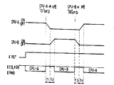
제 2 도는 제 1 도의 시스템 동작을 설명하는 타임차트.2 is a time chart illustrating the system operation of FIG.
제 3 도는 제 1 도 시스템의 실제 회로기판의 구조를 설명하는 사시도.3 is a perspective view illustrating the structure of an actual circuit board of the FIG. 1 system.
* 도면의 주요부분에 대한 부호의 설명* Explanation of symbols for main parts of the drawings
4,5 : 주변회로 6 : 제어레지스터4,5: Peripheral circuit 6: Control register
7 : 제 3 게이트 9 : 제 4 게이트7: third gate 9: fourth gate
10,11 : 복호기 12 : 어드레스버스10,11
13 : 데이타버스 14 : 제어버스13 data bus 14 control bus
15,18 : 마이크로프로세서 16 : 제 1 게이트15,18: microprocessor 16: the first gate
15,18 : 마이크로프로세서 16 : 제 1 게이트15,18: microprocessor 16: the first gate
19 : 제 2 게이트19: second gate
본 발명은 멀티프로세서 시스템, 특히 각종 프로세서의 구조에 관계없이 각종의 프로세서에 자유롭게 스위치되며 예컨대 개인용 컴퓨터등에서 사용되는 멀티프로세서에 관한 것이다. 최근 수년동안 마이크로프로세서는 여러회사에서 개발되고 제조되어 왔으며 이들 마이크로프로세서들은 예컨대 개인용 컴퓨터에 사용된다. 이들 프로세서를 위한 여러가지 형태의 소프트웨어가 개발되어 왔다. 그러나 이와같은 형태의 소프트웨어의 대부분은 통상적으로 상이한 프로세서 사이에 상호 교환하여 사용할 수 없으므로 여러가지 프로세서에 대하여 개발된 상이한 형태의 소프트 웨어가 단일 형태의 컴퓨터에서 사용할 수 있게 하기 위하여 특별한 기술의 사용을 필요로 한다. 단일 형태의 개인용 컴퓨터등이 가능한한 많은 형태의 소프트웨어를 이용할 수 있도록 각 컴퓨터가 다수의 상위한 프로세서를 포함하며, 이들 프로세서들은 변환될 수 있어서 상위한 프로세서에 대해 개발된 소프트웨어의 이용을 가능케 하는 개인용 컴퓨터가 알려졌다. 예를들면 후지쓰사에서 제조된 FM-8형 개인용 컴퓨터에서는 모터로라사에서 제조된 6809형 프로세서와 자이로그사에서 제조한 옵션형 프로세서 Z80형 사이의 변환이 가능하게 함으로써 이들 프로세서 각각을 모두 이용할 수 있게 했다. 또다른 예로 미국 애플사에서 제조한 애플 II형 개인용 컴퓨터에 있어서는 모스텍사에서 제조된 6502형 프로세서와 옵션형인 Z80사이에 변환이 가능하게 함으로서 두가지 형태의 프로세서 이용이 가능하다. 그러나 위에서 언급한 종전의 컴퓨터 시스템은 다른 프로세서를 이용하고저 할때 이미 정해진 특정의 프로세서 사이의 변환만이 가능하다.The present invention relates to a multiprocessor system, in particular a multiprocessor which is freely switched to various processors regardless of the structure of the various processors and used for example in personal computers. In recent years, microprocessors have been developed and manufactured by many companies, and these microprocessors are used, for example, in personal computers. Various forms of software have been developed for these processors. However, most of these types of software typically cannot be used interchangeably between different processors, requiring the use of special techniques to make different types of software developed for different processors available on a single type of computer. do. Each computer includes a number of higher processors so that a single type of personal computer can use as many types of software as possible, and these processors can be converted to a personal computer that allows the use of software developed for the higher processor. The computer is known. For example, an FM-8 personal computer manufactured by Fujitsu Corporation can use each of these processors by allowing conversion between the 6809 processor manufactured by Motorola and the optional processor Z80 manufactured by Zylog. I made it. In another example, Apple's Type II personal computer manufactured by Apple Inc. in the United States allows two types of processors to be converted between the 6502 processor manufactured by Mostek and the optional Z80. However, the conventional computer system mentioned above can only convert between certain processors that are already defined when using other processors.
미리 정해지지 않은 프로세서 사이의 변환은 불가능하며, 따라서 각종 프로세서에 대하여 개발된 소프트웨어를 최대로 이용하는 것이 불가능하다. 더욱이 위에서 언급한 종전의 시스템에서는 주프로세서는 주인쇄회로기판에 영구적으로 부착되어 있으며 또 다른 프로세서가 부착된 인쇄회로기판이 코넥터에 의하여 주 인쇄회로기판과 연결된다.Conversion between processors that are not predetermined is not possible and therefore it is not possible to make full use of software developed for various processors. Moreover, in the conventional system mentioned above, the main processor is permanently attached to the main printed circuit board, and the printed circuit board to which another processor is attached is connected to the main printed circuit board by a connector.
그러므로 사용 가능한 주 프로세서는 특정형태의 컴퓨터 시스템에 사용할 수 있는 것에 한정되며 따라서 이와 다른 형태의 프로세서를 주 프로세서로 사용되는 것은 불가능하다. 종전의 시스템의 상기한 문제점들의 관점에서 본 발명은 각각 이 프로세서를 부착한 다수의 CPU보드를 플러그인형 코넥터등을 사용하여 공통 메모리회로, 입출력 인터페이스회로 및 기타 다른 회로를 부착한 공통 인쇄회로판에 연결하게 하는 것을 가능하도록 하는 사상을 채택한 것이다. 본 발명의 목적은 각종의 프로세서 구조와 관계없이 임의의 종류의 프로세서 사이에 자유로운 변환을 가능하게 함으로써 각종의 프로세서에 대한 소프트웨어의 폭넓은 사용을 가능하게 하려는 데 있다. 본 발명의 또 다른 목적은 어느 프로세서라도 주 프로세서로 사용할 수 있게 함으로써 컴퓨터 시스템이 요구되는 분야에서 가능한한 최대로 사용되는데 있다.Therefore, the main processor available is limited to that which can be used for a particular type of computer system, and therefore it is impossible to use another type of processor as the main processor. In view of the above problems of the previous system, the present invention connects a plurality of CPU boards each equipped with this processor to a common printed circuit board to which a common memory circuit, an input / output interface circuit and other circuits are attached using a plug-in connector or the like. The idea is to make it possible to make it possible. It is an object of the present invention to enable wide use of software for various processors by allowing free conversion between any kind of processor, regardless of the various processor architectures. It is a further object of the present invention to allow any processor to be used as the main processor, thereby maximizing its use in the field where a computer system is required.
본 발명에 따라, 제 1 프로세서 스위치신호와 동작상태 및 중지 상태중 하나를 표시하는 제 1 상태 신호를 발생하는 제 1 마이크로프로세서, 제 2 프로세서 스위치신호와 동작상태 및 중지상태 중 하나를 표시하는 제 2 상태신호를 발생하는 제 2 마이크로프로세서, 상기 제1 및 제 2 마이크로 프로세서에 동작적으로 접속된 공통버스 ; 상기 공통버스에 동작적으로 접속된 주변회로 ; 상기 공통버스에 동작적으로 접속되며 상기 공통버스를 경유하여 상기 제1 및 제 2 마이크로 프로세서에 의해 억세스 가능하며 제1 및 제 2 프로세서 스위치 신호에 의하여 상기 제1 및 제 2 마이크로 프로세서에 대한 중지요청상태를 표시하는 제어신호를 발생하는 제어 레지스터 ; 상기 제 1 마이크로프로세서에 동작적으로 접속되며 상기 제 1 마이크로프로세서를 위하여 제 1 중지요청신호를 수신하여 제 1 상태신호가 제 1 마이크로프로세서가 중지상태에 있다는 것을 표시할 때 제 1 중지긍정신호를 발생하는 제 1 게이트회로 ; 상기 제 2 마이크로프로세서에 동작적으로 접속되며 제 2 마이크로프로세서를 위하여 제 2 중지요청신호를 수신하여 제 2 상태신호가 상기 제 2 마이크로프로세서가 중지상태에 있다는 것을 표시할 때 제 2 중지긍정신호를 발생하는 제 2 게이트회로 ; 상기 제 1 게이트회로, 제 2 중지긍정신호를 수신하는 상기 제 2 게이트회로 및 제어신호를 수신하는 상기 제어레지스터에 동작적으로 접속되며 제어신호가 상기 제 1 마이크로프로세서를 위한 중지요청상태를 표시할 때 제 1 중지요청신호를 발생하며 제어신호가 상기 제 2 마이크로프로세서를 위한 중지요청상태를 표시하고 제 2 중지긍정신호가 수신될 때 제 1 중지요청신호를 출력하는 제 3 게이트회로 ; 및 상기 제 2 게이트회로, 제 1 중지긍정신호를 수신하는 상기 제 1 게이트회로 및 제어신호를 수신하는 상기 제어레지스터에 동작적으로 접속되며, 제어신호가 제 2 마이크로프로세서에 대한 중지요청상태를 표시할 때 제 2 중지요청신호를 발생하고, 제어신호가 상기 제 1 마이크로 프로세서에 대한 중지요청상태를 표시하고 제 1 중지긍정신호가 수신될 때 제 2 중지요청신호를 출력하는 제 4 게이트회로로 구성되는 것을 특징으로 하는 멀티프로세서 시스템이 제공된다.According to the present invention, a first microprocessor for generating a first state signal for indicating a first processor switch signal and one of an operating state and a stop state, and a second microprocessor for generating a first state signal for displaying one of an operating state and a stop state, A second microprocessor for generating a second status signal and a common bus operatively connected to the first and second microprocessors; A peripheral circuit operatively connected to the common bus; Stop request for the first and second microprocessors by means of first and second processor switch signals operatively connected to the common bus and accessible by the first and second microprocessors via the common bus A control register for generating a control signal indicating a status; Operably connected to the first microprocessor and receiving a first stop request signal for the first microprocessor when the first status signal indicates that the first microprocessor is in a suspended state; A first gate circuit generated; Receive a second stop request signal for the second microprocessor and receive a second stop positive signal when a second status signal indicates that the second microprocessor is in a suspended state. A second gate circuit generated; And operatively connected to the first gate circuit, the second gate circuit receiving a second stop positive signal and the control register receiving a control signal, the control signal being indicative of a stop request state for the first microprocessor. A third gate circuit that generates a first stop request signal and outputs a first stop request signal when a control signal indicates a stop request state for the second microprocessor and when a second stop positive signal is received; And a second gate circuit, the first gate circuit for receiving a first stop positive signal, and the control register for receiving a control signal, wherein the control signal indicates a stop request state for the second microprocessor. And a fourth gate circuit for generating a second stop request signal, the control signal indicating a stop request state for the first microprocessor, and outputting a second stop request signal when a first stop positive signal is received. A multiprocessor system is provided which is characterized by the above-mentioned.
제어회로는 제어레지스터의 출력신호와 제어레지스터 출력신호가 동작중인 마이크로프로세서에 의하여 변경될 때 또다른 마이크로프로세서가 중지상태가 있는지를 표시하는 상태신호와 일치하느냐의 여부에 따라 동작중에 있는 마이크로프로세서에 중지요청신호를 전송한다. 그리고 제어회로는 마이크로프로세서가 이미 중지상태에 들어가 있다는 것을 나타내는 상태신호와 제어레지스터의 출력신호가 일치하는지의 여부에 의하여 중지상태에 있는 또다른 마이크로프로세서에 인가되는 중지요청신호를 출력한다.The control circuit applies to the microprocessor in operation whether or not the output signal of the control register and the control register output signal match the status signal indicating whether another microprocessor is in a stopped state when the control register output signal is changed by the operating microprocessor. Send the stop request signal. The control circuit then outputs a stop request signal applied to another microprocessor in the suspended state by whether the status signal indicating that the microprocessor is already in the suspended state matches the output signal of the control register.
본 발명의 실시예를 도면에 입각하여 설명하면 다음과 같다. 제 1 도는 본 발명의 실시예로서 멀티프로세서 시스템의 개략적 구조를 도시한 것이다.An embodiment of the present invention will be described with reference to the drawings. 1 shows a schematic structure of a multiprocessor system as an embodiment of the invention.
제 1 도에서 보인 시스템은 주보드(1), 코넥터등에 의하여 주보드(1)와 연결된 2개의 CPU보드(2,3)로 구성되어 있다. 주보드(1)에 배열된 것은 공통메모리(4), 입출력 인터페이스회로(5), 공통레지스터를 구성하는 플립플롭(6), AND게이트(7,8,9) 및 복호기(10,11)등이다. 또한 어드레스버스(12), 데이타버스(13) 및 제어버스(14)가 제공되어진다.The system shown in FIG. 1 is composed of two
CPU보드(2)에는 제 1 프로세서(CPU-A)(15), 플립플롭(16) 및 NAND게이트(17)등이 제공되어진다. CPU보드(3)는 제 2 프로세서(CPU-B)(18), 플립플롭(19), NAND게이트(20)등이 갖추어져 있다. CPU보드(2)의 프로세서와 CPU보드(3)의 프로세서(18) 각각은 주보드(1)에 있는 어드레스버스(12), 데이타버스(13) 및 제어버스(14)와 연결되어 있다.The
CPU보드(2)의 플립플롭(16)의 입력단자는 신호선(21)을 통하여 주보드(1)의 AND게이트(7)의 출력단자에 연결되어 있다. CPU보드(2)의 NAND게이트(17)의 출력단자는 신호선(22)을 통하여 주보드(1)에 있는 AND게이트(9)의 반전단자에 연결되어 있다.The input terminal of the flip-
CPU보드(3)의 플립플롭(19)의 입력단자는 신호선(23)을 통하여 주보드(1)에 있는 AND게이트(9)의 출력과 연결되어 있으며 CPU보드(3)에 있는 NAND게이트(20)의 출력단자는 신호선(24)을 통해 주보드(1)에 있는 AND게이트(7)의 반전입력단자에 연결되어 있다. CPU보드(2)와 CPU보드(3)에 있는 프로세서(15)와 프로세서(18)사이의 변환은 4개의 신호선(21,22,23,24)을 사용함으로써 이루어진다. CPU보드(2와 3)에 있는 프로세서(15와 18)의 각각으로부터 주보드(1)에 있는 플립플롭(6)에 데이타를 억세스하여 세트하는 것이 가능하다.The input terminal of the flip-
플립플롭(6)을 각 프로세서(15,18)로부터 교대로 억세스하기 위하여 플립플롭은 한개의 어드레스(예를들어 $FD05)를 가진다. 데이타를 각각의 프로세서(15와 18)로부터 플립플롭(6)에 기입할때 어드레스(&FD05)를 지정하는 어드레스 데이타를 어드레스(12)에 보내고 가입데이타는 데이타버스로 보낸다. 어드레스버스(12)에 보내진 어드레스 데이타는 복호기(10)에 의하여 복호화하며 AND게이트(8)를 경유하여 플립플롭(6)의 클록입력단자(C)에 인가된다. 이때 AND게이트(8)는 제어버스(14)로부터 공급되는 제어신호에 의하여 열린다.In order to alternately access flip-flop 6 from each
데이타버스(13)에 보내진 데이타중에서 최의미비트(LSB)는 플립플롭(6)의 데이타 입력단자(D)에 입력된다. 상기의 구조를 사용하여 어드레스(&FD05)를 지정함으로써 각 프로세서(15와 18)로부터 플립플롭(6)에 기입이 가능하다. 제 2 도에 의거하여 제 1 도의 시스템동작을 설명하겠다. 리세트신호(*RST)는 (여기서 *표는 논리신호를 반전시키는 것을 나타냄)주보드(1)의 플립플롭(6)에 인가되어져서 로우(low)상태로 변하며 플립플롭(6)의 리세트가 실행되어 출력(Q)이 로우가 되고,![]()
![]()
![]()
![]()
이런 상태에서 어드레스신호, 데이타신호 및 기본적 제어신호(예 *EB, *QB 및 판독기입제어신호(read write control signal : RWB)가 프로세서(15)로부터 주보드(1)에 필요에 따라 입력된다.In this state, an address signal, a data signal and a basic control signal (e.g., * EB, * QB and read write control signal RWB) are input from the
다시말해 시스템이 리스타트한 후에 프로세서(15)가 동작할 때 프로세서(18)는 중지상태에 들어간다. 프로세서(15)가 위에서 언급한 것과 같이 동작상태에 있으며 프로세서(15)에서 프로세서(18)로 동작하는 프로세서를 전환시켜야 할때 데이타("1")를 프로세서(15)로부터 어드레스 (&FD05)에 기입한다.In other words, when the
그러므로 주보드(1)에 있는 플립플롭(6)은 세트로 되고 출력(Q와![]()
![]()
![]()
![]()
그렇게 됨으로써 프로세서(18)는 동작상태에 들어가게 되고 어드레스신호, 데이타신호 및 제어신호(*EB, *QB, *RWB 등)는 프로세서(18)로부터 주보드(1)에 전송된다. CPU보드(2와 3)에 있는 플립플롭(16 및 19)에 인가되는 내부클록(CKA와 CKB)은 중지요청신호가 각 CPU보드에 입력이 될때 대응되는 CPU보드의 내부타이밍에 따라서 각각 플립플롭(16 및 19)을 세트시키거나 리세트시키는데 사용되며 이에 의해 CPU보드 사이에 동작 타이밍을 조정한다.By doing so, the
CPU-A가 어드레스(&FD05)에 "1"을 써넣을 때 CPU-A가 순간적으로 중지하는 것이 아니라 현재 사용중에 있는 명령의 수행이 완료된 후에야 중단된다. 즉 CPU-A가 중단되는데는 T1만큼의 미확정시간이 필요한 것이다(제 2 도 참조).When CPU-A writes " 1 " at address & FD05, CPU-A does not stop momentarily but only after completion of the instruction currently being used. In other words, the undetermined time as much as T1 is required to stop the CPU-A (see Fig. 2).
또한 CPU-B가 중지상태에서 동작상태로 변환되는데는 미확정시간(T2)이 필요하며 이를 위하여는 동작모드(Mode)를 갖는다(제 2 도 참조).In addition, the CPU-B requires an undetermined time T2 for the transition from the suspended state to the operating state, and has an operation mode (see FIG. 2).
그러므로 CPU-A가 데이타("1")를 어드레스(&FD05)에 기입한 직후의 시점과 CPU-B가 완전히 동작상태에 들어간 시점사이에서 메모리와 입출력장치에 대한 제어신호(*EB, *QB, *RWB)를 불능 즉 하이레벨 상태로 유지시킬 필요가 있다. 그러나, 예외로서 파이프라인 제어를 실시하는 8088이나 8086형등의 프로세서에서는 때때로 제어신호(*EB, *QB, *RWB 등)가 데이타(예를 들어 "1")를 어드레스(&FD05)에 기입한 후 즉시 불능상태로 하는 것은 부적합하다.Therefore, between the time immediately after CPU-A writes data (" 1 ") to address & FD05 and the time CPU-B is fully operational, the control signals (* EB, * QB, It is necessary to keep * RWB) disabled, or at a high level. However, in the 8088 or 8086 type processor which performs pipeline control as an exception, sometimes a control signal (* EB, * QB, * RWB, etc.) writes data (for example, "1") to address & FD05. It is inappropriate to disable it immediately.
따라서, 이런 종류의 프로세서를 멀티프로세서 시스템에서 사용할때는 제어신호(*EB, *QB, *RWB 등)가 즉시 사용금지 상태가 되지 않도록 해당 CPU보드내에 제어회로를 설치할 필요가 있다. CPU-A CPU-B가 상기 방식으로 중지상태와 동작상태에 있을 때 CPU-B의 동작을 다시 중단시키고 CPU-A를 동작시킬 필요가 있으며 데이타("0")를 CPU-B으로부터 상기한 어드레스(&FD05)에 기입시키면 된다. 데이타("0")를 어드레스(&FD05)에 기입할 때 플립플롭(6)을 리세트 상태로함으로써 플립플롭(6)의 출력(Q와![]()
![]()
그러므로 중지요청신호는 위에서 언급한 방법과 유사한 방법으로 CPU보드(3)에 입력되어 CPU-B는 중지상태로 변하고 CPU-A는 동작상태로 된다. 이 경우에 동작은 플립플롭(6)의 리세트를 해제시킬 때의 방법과 동일하고 이미 설명하였으므로 생략하기로 하자.Therefore, the stop request signal is input to the CPU board 3 in a manner similar to the above-mentioned method so that the CPU-B is changed to the suspended state and the CPU-A is brought into the operation state. In this case, the operation is the same as the method for releasing the reset of the flip-flop 6, and since it has already been described, it will be omitted.
제 1 도에서 복호기(11)는 어드레스버스(12)에서 보내진 어드레스 데이타중 상위비트(bit)를 복호화하는데 사용되며 칩선택신호를 선택된 메모리 칩(4)의 칩선택단자( cs : chip select)에 인가하기 위하여 사용된다. 또한 어드레스 데이타중 하위비트는 메모리 칩(4)에 입력이 되고 메모리 칩내에서 어드레스는 지정하는데 사용된다.In FIG. 1, the decoder 11 is used to decode the upper bit of the address data sent from the
제 3 도는 본 발명의 실시예로써 멀티프로세서 시스템의 실제 회로기판의 구조를 설명하는 것이다. 제 3 도에 표시된 바와같이 코넥터(25,26,27) 및 공통메모리(4)와 입출력 인터페이스회로(15)가 주보드(1)에 배열되어 있다. 코넥터(25)와 (26)는 CPU보드(2와 3)에 각각 연결되어 있다. 코넥터(27)는 예를들어 플로피 디스크장치, 디스플레이 장치등과 같은 주변장치를 위한 인터페이스회로를 부가적으로 연결시키거나 또는 다른 회로를 연결시키기 위하여 구비되어 있다.3 illustrates the structure of an actual circuit board of a multiprocessor system according to an embodiment of the present invention. As shown in FIG. 3, the
CPU보드(2와 3)에 연결되어 있는 코넥터(25와 26)는 버스선에 연결되어 있다. 이때 버스선은 주보드(1)에 배설되어 있으며 공통메모리(4)와 입출력회로(5)등과 연결되어 있다. 또한 버스선은 데이타버스(12), 어드레스버스(13), 제어버스(14) 및 CPU보드(2 및 3)위에 설치된 프로세서를 변환시키기 위한 신호선(21,22,23,24)을 포함하고 있다.The
제 3 도에서 보인 구조에서 다른 프로세서가 부착되어 있는 CPU보드를 CPU보드(2,3)에 대신하여 코넥터(25와 26)에 끼워 넣을 수 있으며 신호선(21,22,23,24)을 사용함으로써 원하는 프로세서를 가지고 있는 CPU보드를 포함하고 있는 CPU보드의 동작을 쉽게 변환시킬 수 있다.In the structure shown in FIG. 3, a CPU board to which another processor is attached can be inserted into the
또한 이것은 8-비트 CPU와 16-비트 CPU의 사용을 가능하게 한다. 예를들면 인텔사에서 제조하는 8086이나 80286형 프로세서 또는 모터로라에서 제조되는 68000형의 프로세서를 같이 사용할 수 있는데 이것은 16비트 CPU와 양립할 수 있는 버스선들을 사용하므로서 가능하다.This also allows the use of 8-bit CPUs and 16-bit CPUs. For example, you can use an Intel 8086 or 80286 processor or a 68000 processor from Motorola, which uses bus lines that are compatible with 16-bit CPUs.
본 발명에 의하면 이와같은 방법으로 각기 임의 종류의 프로세서가 부착되어 있는 다수의 CPU보드를 주보드에 연결시킬 수 있으며 적은 수의 신호선을 사용하므로서 CPU보드의 동작을 변환시킬 수 있다.According to the present invention, a plurality of CPU boards to which any kind of processor is attached can be connected to the main board in this manner, and the operation of the CPU board can be converted by using a small number of signal lines.
그러므로 개인용 컴퓨터의 각 프로세서등을 위하여 개발된 소프트웨어를 보다 잘 이용할 수 있는 것이다. 더욱이 각 CPU보드의 동작변환이 적은수의 신호선을 사용하고도 가능하기 때문에 멀티프로세서 시스템의 구조는 간략화 될 수 있으며 그 신뢰성이 개선된다.Therefore, you can better use the software developed for each processor of the personal computer. Moreover, since the operation conversion of each CPU board can use a small number of signal lines, the structure of the multiprocessor system can be simplified and its reliability is improved.
Claims (8)
Applications Claiming Priority (3)
| Application Number | Priority Date | Filing Date | Title |
|---|---|---|---|
| JP115885 | 1983-06-29 | ||
| JP???58-115885 | 1983-06-29 | ||
| JP58115885A JPS608972A (en) | 1983-06-29 | 1983-06-29 | Multi-processor system |
Publications (2)
| Publication Number | Publication Date |
|---|---|
| KR850000718A KR850000718A (en) | 1985-02-28 |
| KR890002330B1 true KR890002330B1 (en) | 1989-06-30 |
Family
ID=14673589
Family Applications (1)
| Application Number | Title | Priority Date | Filing Date |
|---|---|---|---|
| KR1019840003581A KR890002330B1 (en) | 1983-06-29 | 1984-06-25 | Multi processor sytem |
Country Status (5)
| Country | Link |
|---|---|
| US (1) | US4716526A (en) |
| EP (1) | EP0130733B1 (en) |
| JP (1) | JPS608972A (en) |
| KR (1) | KR890002330B1 (en) |
| DE (1) | DE3483029D1 (en) |
Families Citing this family (31)
| Publication number | Priority date | Publication date | Assignee | Title |
|---|---|---|---|---|
| JPS62168258A (en) * | 1986-01-20 | 1987-07-24 | Victor Co Of Japan Ltd | Cpu switching circuit |
| US4920481A (en) * | 1986-04-28 | 1990-04-24 | Xerox Corporation | Emulation with display update trapping |
| US5088033A (en) * | 1986-04-28 | 1992-02-11 | Xerox Corporation | Data processing system emulation in a window with a coprocessor and I/O emulation |
| US5297272A (en) * | 1989-08-02 | 1994-03-22 | Advanced Logic Research, Inc. | Apparatus for automatically disabling and isolating a computer's original processor upon installation of a processor upgrade card |
| US5201055A (en) * | 1989-11-03 | 1993-04-06 | Compaq Computer Corporation | Multiprocessing system includes interprocessor encoding and decoding logic used for communication between two cards through reduced addressing lines |
| JP3118266B2 (en) * | 1990-03-06 | 2000-12-18 | ゼロックス コーポレイション | Synchronous segment bus and bus communication method |
| US5280283A (en) * | 1990-11-09 | 1994-01-18 | Ast Research, Inc. | Memory mapped keyboard controller |
| US5261114A (en) * | 1990-11-09 | 1993-11-09 | Ast Research, Inc. | Method and apparatus for providing down-loaded instructions for execution by a peripheral controller |
| WO1992018936A1 (en) * | 1991-04-18 | 1992-10-29 | Intel Corporation | Method and apparatus for upgrading a computer processing system |
| EP0510241A3 (en) * | 1991-04-22 | 1993-01-13 | Acer Incorporated | Upgradeable/downgradeable computer |
| US5761479A (en) * | 1991-04-22 | 1998-06-02 | Acer Incorporated | Upgradeable/downgradeable central processing unit chip computer systems |
| US5551012A (en) * | 1991-04-22 | 1996-08-27 | Acer Incorporated | Single socket upgradeable computer motherboard with automatic detection and socket reconfiguration for inserted CPU chip |
| EP0529142A1 (en) * | 1991-08-30 | 1993-03-03 | Acer Incorporated | Upgradeable/downgradeable computers |
| US5473766A (en) * | 1991-09-11 | 1995-12-05 | Compaq Computer Corp. | Signal routing circuit for interchangeable microprocessor socket |
| WO1993007567A1 (en) * | 1991-10-11 | 1993-04-15 | Martin Giger | Multi business computer with multi-processor architecture |
| WO1994019749A1 (en) * | 1993-02-26 | 1994-09-01 | Chou Benjamin E | Computer system for sharing common system resources with two or more independently operating microcomputers |
| US5490279A (en) * | 1993-05-21 | 1996-02-06 | Intel Corporation | Method and apparatus for operating a single CPU computer system as a multiprocessor system |
| US6401158B1 (en) * | 1993-07-16 | 2002-06-04 | Compaq Computer Corporation | Apparatus for providing a CPU cluster via a disk I/O bus using a CPU brick which fits into a disk cavity |
| US5586270A (en) * | 1993-09-30 | 1996-12-17 | Intel Corporation | Method and apparatus for upgrading a central processing unit and existing memory structure in a computer system |
| US5495588A (en) * | 1993-11-18 | 1996-02-27 | Allen-Bradley Company, Inc. | Programmable controller having joined relay language processor and general purpose processor |
| US5884091A (en) * | 1993-12-08 | 1999-03-16 | Intel Corporation | Computer system having a central processing unit responsive to the identity of an upgrade processor |
| US5384692A (en) * | 1993-12-16 | 1995-01-24 | Intel Corporation | Socket with in-socket embedded integrated circuit |
| KR0119795B1 (en) * | 1994-04-20 | 1997-10-27 | 김광호 | Computer easy for up-grade |
| EP0803130B1 (en) * | 1994-06-29 | 2007-02-28 | Intel Corporation | Processor that indicates system bus ownership in an upgradable multiprocessor computer system |
| US5748912A (en) * | 1995-06-13 | 1998-05-05 | Advanced Micro Devices, Inc. | User-removable central processing unit card for an electrical device |
| US6513057B1 (en) | 1996-10-28 | 2003-01-28 | Unisys Corporation | Heterogeneous symmetric multi-processing system |
| US5987553A (en) * | 1997-09-22 | 1999-11-16 | Dell Computer Corporation | Adaptor board interconnection for a processor board and motherboard |
| US6851002B1 (en) * | 1998-04-01 | 2005-02-01 | Omron Corporation | Processing device with parallel mounting regions for component exchange |
| US20020087828A1 (en) * | 2000-12-28 | 2002-07-04 | International Business Machines Corporation | Symmetric multiprocessing (SMP) system with fully-interconnected heterogenous microprocessors |
| US20040123070A1 (en) * | 2002-12-23 | 2004-06-24 | Shidla Dale J. | Automatic detection of different microprocessor architectures |
| JP2005235043A (en) * | 2004-02-23 | 2005-09-02 | Fujitsu Ltd | Information processing unit and method |
Family Cites Families (6)
| Publication number | Priority date | Publication date | Assignee | Title |
|---|---|---|---|---|
| US4390943A (en) * | 1979-12-26 | 1983-06-28 | Honeywell Information Systems Inc. | Interface apparatus for data transfer through an input/output multiplexer from plural CPU subsystems to peripheral subsystems |
| US4420806A (en) * | 1981-01-15 | 1983-12-13 | Harris Corporation | Interrupt coupling and monitoring system |
| US4547849A (en) * | 1981-12-09 | 1985-10-15 | Glenn Louie | Interface between a microprocessor and a coprocessor |
| JPS58205272A (en) * | 1982-05-25 | 1983-11-30 | Kokusai Electric Co Ltd | Alternate operating device for two computers with different functions |
| US4590556A (en) * | 1983-01-17 | 1986-05-20 | Tandy Corporation | Co-processor combination |
| US4591975A (en) * | 1983-07-18 | 1986-05-27 | Data General Corporation | Data processing system having dual processors |
-
1983
- 1983-06-29 JP JP58115885A patent/JPS608972A/en active Granted
-
1984
- 1984-06-19 EP EP84304146A patent/EP0130733B1/en not_active Expired - Lifetime
- 1984-06-19 DE DE8484304146T patent/DE3483029D1/en not_active Expired - Fee Related
- 1984-06-20 US US06/622,455 patent/US4716526A/en not_active Expired - Lifetime
- 1984-06-25 KR KR1019840003581A patent/KR890002330B1/en not_active IP Right Cessation
Also Published As
| Publication number | Publication date |
|---|---|
| KR850000718A (en) | 1985-02-28 |
| EP0130733A2 (en) | 1985-01-09 |
| EP0130733B1 (en) | 1990-08-22 |
| DE3483029D1 (en) | 1990-09-27 |
| JPS648387B2 (en) | 1989-02-14 |
| JPS608972A (en) | 1985-01-17 |
| EP0130733A3 (en) | 1987-07-22 |
| US4716526A (en) | 1987-12-29 |
Similar Documents
| Publication | Publication Date | Title |
|---|---|---|
| KR890002330B1 (en) | Multi processor sytem | |
| EP0087367B1 (en) | Interchangeable interface circuitry arrangements for use with a data processing system | |
| KR900004006B1 (en) | Micro processor system | |
| EP0506021A1 (en) | Method and apparatus for providing initial instructions in a multiple computer system | |
| US5093780A (en) | Inter-processor transmission system having data link which automatically and periodically reads and writes the transfer data | |
| US4282572A (en) | Multiprocessor memory access system | |
| EP0057511B1 (en) | Information processing unit | |
| US4780822A (en) | Semaphore circuit for shared memory cells | |
| US5001625A (en) | Bus structure for overlapped data transfer | |
| US3651473A (en) | Expandable interlock exchange for multiprocessing systems | |
| US4631667A (en) | Asynchronous bus multiprocessor system | |
| US5467461A (en) | Multiprocessor computer system having bus control circuitry for transferring data between microcomputers | |
| US4947478A (en) | Switching control system for multipersonality computer system | |
| GB2060961A (en) | Data processing system having memory modules with distributed address information | |
| JPS6242306B2 (en) | ||
| KR910001708B1 (en) | Central processing unit | |
| GB2060943A (en) | Electronic control for timing hammers in impact printers | |
| US5823871A (en) | Interface control device for use with TV game equipment | |
| US4472773A (en) | Instruction decoding logic system | |
| US4916601A (en) | Means for transferring firmware signals between a control store and a microprocessor means through a reduced number of connections by transfer according to firmware signal function | |
| US4330842A (en) | Valid memory address pin elimination | |
| KR920003479Y1 (en) | Data transmission circuit of graphic card for p.c. | |
| SU1425692A2 (en) | Two-channel device for interfacing two electronic computers | |
| KR940001558B1 (en) | Processor board state checking apparatus | |
| RU2053546C1 (en) | Input-output processor |
Legal Events
| Date | Code | Title | Description |
|---|---|---|---|
| A201 | Request for examination | ||
| E902 | Notification of reason for refusal | ||
| G160 | Decision to publish patent application | ||
| E701 | Decision to grant or registration of patent right | ||
| GRNT | Written decision to grant | ||
| FPAY | Annual fee payment |
Payment date: 20000624 Year of fee payment: 12 |
|
| LAPS | Lapse due to unpaid annual fee |