KR890002311B1 - 과전압 보호 회로 - Google Patents
과전압 보호 회로 Download PDFInfo
- Publication number
- KR890002311B1 KR890002311B1 KR1019840002628A KR840002628A KR890002311B1 KR 890002311 B1 KR890002311 B1 KR 890002311B1 KR 1019840002628 A KR1019840002628 A KR 1019840002628A KR 840002628 A KR840002628 A KR 840002628A KR 890002311 B1 KR890002311 B1 KR 890002311B1
- Authority
- KR
- South Korea
- Prior art keywords
- diode
- protection circuit
- overvoltage protection
- voltage
- gas arrester
- Prior art date
Links
- 230000002159 abnormal effect Effects 0.000 description 24
- 238000010586 diagram Methods 0.000 description 14
- 239000007787 solid Substances 0.000 description 6
- 239000006096 absorbing agent Substances 0.000 description 3
- 230000000694 effects Effects 0.000 description 3
- 230000035939 shock Effects 0.000 description 2
- 230000000977 initiatory effect Effects 0.000 description 1
- 230000009545 invasion Effects 0.000 description 1
Images


Classifications
-
- H—ELECTRICITY
- H02—GENERATION; CONVERSION OR DISTRIBUTION OF ELECTRIC POWER
- H02H—EMERGENCY PROTECTIVE CIRCUIT ARRANGEMENTS
- H02H9/00—Emergency protective circuit arrangements for limiting excess current or voltage without disconnection
- H02H9/04—Emergency protective circuit arrangements for limiting excess current or voltage without disconnection responsive to excess voltage
- H02H9/06—Emergency protective circuit arrangements for limiting excess current or voltage without disconnection responsive to excess voltage using spark-gap arresters
Landscapes
- Emergency Protection Circuit Devices (AREA)
Abstract
Description
Claims (1)
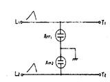
- 제1 및 제 2 다이오드(D1, D2)의 캐소우드를 공통접속하여 제 1 공통점(a)으로하고 그들의 애노드를 각각 선로에 접속하며, 제3 및 제 4 다이오드(D3, D4)의 애노드를 공통 접속하여 제 2 공통점(b)으로하고 그들의 캐소우드를 각각 선로에 접속한 것에 있어서, 상기 제1 및 제 2 공통점(a,b)사이에는 1개의 2극형 가스 피뢰기(Arr3) 및 제너다이오드(ZD)를 병렬 접속하되, 제 1 공통점(a)에는 제 5 다이오드(D5)의 캐소우드를 연결하여 그 애노드를 접지하고, 제 2 공통점(b)에는 제 6 다이오드(D6)의 애노드를 연결하며 그 캐소우드를 접지하여서 구성된 과전압 보호 회로.
Applications Claiming Priority (2)
| Application Number | Priority Date | Filing Date | Title |
|---|---|---|---|
| JP58252197A JPS60141127A (ja) | 1983-12-28 | 1983-12-28 | 過電圧保護回路 |
| JP?58-252197 | 1983-12-28 |
Publications (2)
| Publication Number | Publication Date |
|---|---|
| KR850005179A KR850005179A (ko) | 1985-08-21 |
| KR890002311B1 true KR890002311B1 (ko) | 1989-06-28 |
Family
ID=17233849
Family Applications (1)
| Application Number | Title | Priority Date | Filing Date |
|---|---|---|---|
| KR1019840002628A KR890002311B1 (ko) | 1983-12-28 | 1984-05-15 | 과전압 보호 회로 |
Country Status (2)
| Country | Link |
|---|---|
| JP (1) | JPS60141127A (ko) |
| KR (1) | KR890002311B1 (ko) |
Families Citing this family (1)
| Publication number | Priority date | Publication date | Assignee | Title |
|---|---|---|---|---|
| EP0495980A4 (en) * | 1990-08-14 | 1993-06-23 | Mitsubishi Mining & Cement Co., Ltd. | Circuit connection device having overvoltage/overcurrent protection function |
Family Cites Families (1)
| Publication number | Priority date | Publication date | Assignee | Title |
|---|---|---|---|---|
| JPS57193934A (en) * | 1981-05-25 | 1982-11-29 | Nippon Telegraph & Telephone | Lightning surge protecting circuit |
-
1983
- 1983-12-28 JP JP58252197A patent/JPS60141127A/ja active Granted
-
1984
- 1984-05-15 KR KR1019840002628A patent/KR890002311B1/ko not_active IP Right Cessation
Also Published As
| Publication number | Publication date |
|---|---|
| JPH0347053B2 (ko) | 1991-07-18 |
| JPS60141127A (ja) | 1985-07-26 |
| KR850005179A (ko) | 1985-08-21 |
Similar Documents
| Publication | Publication Date | Title |
|---|---|---|
| US4683514A (en) | Surge voltage protective circuit arrangements | |
| EP0165347B1 (en) | Protection circuit for a power distribution system | |
| US6195245B1 (en) | Low capacitance surge protector for high speed data transmission | |
| US5781392A (en) | Balanced overvoltage protector for a dual-wire system | |
| US20050063118A1 (en) | Multipole overvoltage protection system and method for the reliable operation of a multipole overvoltage protection system | |
| JPH0145812B2 (ko) | ||
| KR890002311B1 (ko) | 과전압 보호 회로 | |
| US4439802A (en) | Overvoltage guard for electronic circuits | |
| US6628497B1 (en) | Overvoltage protector bridge circuit | |
| WO1987000984A1 (en) | Surge voltage protection arrangements | |
| EP0185777A1 (en) | Safety circuit system for overvoltage protection of multi-wire lines | |
| JPS63294218A (ja) | 火花ギャップ式高速度避雷器 | |
| JPH0419949Y2 (ko) | ||
| JP2000050494A (ja) | 同軸ケーブル用避雷器 | |
| JPH0419950Y2 (ko) | ||
| US20250023342A1 (en) | Surge protection circuit | |
| KR102345726B1 (ko) | 다중 접지형 서지 보호장치 | |
| JPH0336207Y2 (ko) | ||
| SU1669026A1 (ru) | Многозазорный искровой разр дник | |
| SU1120448A1 (ru) | Устройство дл защиты от перенапр жений высоковольтного распределительного устройства | |
| JPH0562150U (ja) | 通信線路用サージ保護装置 | |
| JPS60144115A (ja) | 共通線を用いた多回線保安回路 | |
| SU1163414A1 (ru) | Устройство защиты линии и аппаратуры проводной св зи от импульсных перенапр жений | |
| JPH1141798A (ja) | 雷防護アダプタ | |
| SU1169074A1 (ru) | Ограничитель внутренних перенапряжений |
Legal Events
| Date | Code | Title | Description |
|---|---|---|---|
| A201 | Request for examination | ||
| PA0109 | Patent application |
Patent event code: PA01091R01D Comment text: Patent Application Patent event date: 19840515 |
|
| PA0201 | Request for examination | ||
| PG1501 | Laying open of application | ||
| E902 | Notification of reason for refusal | ||
| PE0902 | Notice of grounds for rejection |
Comment text: Notification of reason for refusal Patent event date: 19890309 Patent event code: PE09021S01D |
|
| G160 | Decision to publish patent application | ||
| PG1605 | Publication of application before grant of patent |
Comment text: Decision on Publication of Application Patent event code: PG16051S01I Patent event date: 19890529 |
|
| E701 | Decision to grant or registration of patent right | ||
| PE0701 | Decision of registration |
Patent event code: PE07011S01D Comment text: Decision to Grant Registration Patent event date: 19890912 |
|
| GRNT | Written decision to grant | ||
| PR0701 | Registration of establishment |
Comment text: Registration of Establishment Patent event date: 19891104 Patent event code: PR07011E01D |
|
| PR1002 | Payment of registration fee |
Payment date: 19891104 End annual number: 10 Start annual number: 1 |
|
| PR1001 | Payment of annual fee |
Payment date: 19990520 Start annual number: 11 End annual number: 11 |
|
| FPAY | Annual fee payment |
Payment date: 20000512 Year of fee payment: 12 |
|
| PR1001 | Payment of annual fee |
Payment date: 20000512 Start annual number: 12 End annual number: 12 |
|
| LAPS | Lapse due to unpaid annual fee | ||
| PC1903 | Unpaid annual fee |