KR890002311B1 - Over voltage protecting circuit - Google Patents
Over voltage protecting circuit Download PDFInfo
- Publication number
- KR890002311B1 KR890002311B1 KR1019840002628A KR840002628A KR890002311B1 KR 890002311 B1 KR890002311 B1 KR 890002311B1 KR 1019840002628 A KR1019840002628 A KR 1019840002628A KR 840002628 A KR840002628 A KR 840002628A KR 890002311 B1 KR890002311 B1 KR 890002311B1
- Authority
- KR
- South Korea
- Prior art keywords
- diode
- protection circuit
- gas arrester
- overvoltage protection
- voltage
- Prior art date
Links
Images


Classifications
-
- H—ELECTRICITY
- H02—GENERATION; CONVERSION OR DISTRIBUTION OF ELECTRIC POWER
- H02H—EMERGENCY PROTECTIVE CIRCUIT ARRANGEMENTS
- H02H9/00—Emergency protective circuit arrangements for limiting excess current or voltage without disconnection
- H02H9/04—Emergency protective circuit arrangements for limiting excess current or voltage without disconnection responsive to excess voltage
- H02H9/06—Emergency protective circuit arrangements for limiting excess current or voltage without disconnection responsive to excess voltage using spark-gap arresters
Abstract
Description
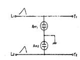
제 1 도는 종래의 과전압 보호 회로의 기본적인 일예를 표시하는 접속도.1 is a connection diagram showing a basic example of a conventional overvoltage protection circuit.
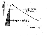
제 2 도는 종래 2개의 가스 피뢰기를 사용했을 경우의 방전 개시 전압의 차와 선간 전압의 발생과의 관계를 표시한 특성도.2 is a characteristic diagram showing the relationship between the difference in discharge start voltage and the generation of line voltage when two gas arresters are used.
제 3 도는 본 발명인 과전압 보호 회로의 제 1 실시예를 표시한 접속도.3 is a connection diagram showing a first embodiment of the overvoltage protection circuit of the present invention.
제 4 도는 본 발명인 과전압 보호 회로의 사용예를 표시한 회로도.4 is a circuit diagram showing an example of use of the overvoltage protection circuit of the present invention.
제 5 도는 본 발명인 과전압 보호 회로의 제 2 실시예를 표시한 접속도.5 is a connection diagram showing a second embodiment of the overvoltage protection circuit of the present invention.
제 6 도는 제너다이오드등 고속으로 응답하는 고체소자를 접속시킨 경우와 접속하지 않은 경우에 대하여 가스 피뢰기의 방전개시 전압차를 표시한 동작 특성도.6 is an operating characteristic diagram showing the discharge start voltage difference of the gas arrester in the case where a solid-state element such as a zener diode which responds at high speed is connected or not.
* 도면의 주요부분에 대한 부호의 설명* Explanation of symbols for main parts of the drawings
1 : 케이블 2 : 피보호 기기1 Cable 2 Protected Equipment
Arr1-Arr3: 가스 피뢰기 D1-D6: 다이오드Arr 1 -Arr 3 : Gas Arrester D 1 -D 6 : Diode
ZD : 제너다이오드.ZD: Zener Diode.
본 발명은 통신 케이블이나 제어 케이블, 계축장치용 케이블등 각종 신호 회선에 침입하는 낙뢰 서어지 전압(충격전압)이나 상용 주파수 등에서 이상전압에 대하여 통신기, 제어장치 및 계측장치등의 기기를 보호하는 과전압 보호회로에 관한 것으로서, 특히 1개의 2극형 가스피뢰기를 사용하여 선간 이상전압이 발생하지 않도록하여 침입하는 정,부극성의 이상전압으로 부터 피보호 기기를 완전하게 보호할 수 있도록한 과전압 보호회로에 관한 것이다. 일반적으로 종래로부터 사용되고 있는 과전압 보호회로에서는, 케이블 심선과 접지사이에 발생하는 이상 전압을 제어하기 위하여 2개의 2극형 가스 피뢰기를 사용하고 있는 실정이다. 그러나 2개의 가스 피뢰기의 자체특성의 미세한 차이 및 선로의 저항 특성 및 가스 피뢰기와 선로 사이에서의 접속 특성이 다르고, 또한 각 피뢰기 마다 그 특성이 동일하지 않기 때문에 2개의 가스 피뢰기는 서로 다른 방전개시 전압 특성을 갖게 된다. 즉, 방전개시 전압에 차이가 있게 된다. 따라서 이러한 방전개시 전압의 차이에 기인하여 선간에는 이상전압이 발생된다. 이러한 선간 이상 전압은 종종 피보호 기기를 파괴한다.The present invention protects the devices such as communication devices, control devices and measuring devices against abnormal voltages at lightning surge voltages (impact voltages) or commercial frequencies invading various signal lines such as communication cables, control cables and cabling devices. In particular, a protection circuit is provided. In particular, an overvoltage protection circuit which completely protects a protected device from positive and negative polarity invasion by preventing the occurrence of abnormal voltage between lines by using a single 2-pole gas arrester. It is about. In general, in the overvoltage protection circuit conventionally used, two dipole type gas arresters are used to control the abnormal voltage generated between the cable core wire and the ground. However, the two gas arresters have different discharge initiation voltages because of the slight differences in the characteristics of the two gas arresters, the resistance of the lines and the connection characteristics between the gas arresters and the lines, and the characteristics of the arresters are not the same. Will have characteristics. That is, there is a difference in the discharge start voltage. Therefore, an abnormal voltage is generated between the lines due to the difference in the discharge start voltage. These line abnormal voltages often destroy the protected equipment.
제 1 도는 종래의 과전압 보호회로의 기본적인 일예를 도시한 접속도이다. 도면에서 Arr1과 Arr2는 가스 피뢰기 L1과 L2는 선로와의 접속단자 T1, T2는 피보호 기거와의 접속단자를 표시한다. 제 1 도에서 도시된 바와같이 종래의 과전압 보호회로에서는, 2개의 2극형 가스 피뢰기(Arr1,Arr2또는 1개의 3극형 가스 피뢰기)를 사용하여 케이블 심선과 접지사이에 발생하는 이상전압을 흡수방전 하도록 하고 있다. 그러나 이와같은 2개의 2극형 가스 피뢰기의 방전 개시 전압의 차에 기인하여 선간 이상전압이 발생한다.1 is a connection diagram showing a basic example of a conventional overvoltage protection circuit. In the figure, Arr 1 and Arr 2 indicate the gas arresters L 1 and L 2 , the connection terminals T 1 and T 2 , respectively. In the conventional overvoltage protection circuit as shown in FIG. 1, two bipolar gas arresters (Arr 1 , Arr 2 or one tripolar gas arrester) are used to absorb abnormal voltages generated between the cable core and the ground. To discharge. However, an abnormal voltage between lines occurs due to the difference in discharge start voltages of the two bipolar gas arresters.
제 2 도는 2개의 2극형 가스 피뢰기를 사용했을 경우의 각각의 방전개시 사이에서의 전압차와 전압발생과의 관계를 표시하는 특성도이다. 이와같이 2개의 2극형 가스 피뢰기를 사용하면 한쪽 가스 피뢰기가 방전을 개시하여도 다른 한쪽 가스 피뢰기는 방전하지 않은 상태가 생기게 된다. 이와같은 방전 개시 전압이 서로 다르고 한쪽만이 방전하면 사선부로 표시되는 시간내에서는 한쪽은 접지전위가 되지만 다른쪽은 이상전압이 그대로 남아 선간 이상전압이 발생한다. 그리고 이 선간 이상전압 때문에 피보호 기기가 파괴되는 일이 있었다. 본 발명의 과전압 보호 회로에서는 종래의 과전압 보호회로에서아 같은 결점을 해결하고 가스 피뢰기의 방전개시 전압차가 발생하지 않도록 하여 선간 이상전압 발생을 억제함으로서 피보호 기기를 완전하게 보호할수 있도록함이 목적이다. 그러기 위하여 본 발명인 과전압 보호 회로에서는 1개의 2극형 가스 피뢰기만을 사용하여 정, 부양극성 이상전압의 침입을 저지할수 있도록 하였다.2 is a characteristic diagram showing the relationship between the voltage difference and the voltage generation between the start of discharge when two bipolar gas arresters are used. Thus, when two bipolar gas arresters are used, even if one gas arrester starts to discharge, the other gas arrester will not be discharged. If the discharge start voltages are different from each other and only one side discharges, one side becomes the ground potential within the time indicated by the hatched portion, but the other side causes the abnormal voltage to remain. In addition, the protected device may be destroyed due to the abnormal line voltage. In the overvoltage protection circuit of the present invention, it is an object of the conventional overvoltage protection circuit to solve the same shortcomings and prevent the occurrence of voltage difference between the start of discharge of the gas arrester so as to suppress the occurrence of abnormal voltage between the lines to completely protect the protected equipment. . To this end, in the overvoltage protection circuit of the present invention, only one bipolar gas arrester is used to prevent intrusion of positive and negative polarity abnormal voltages.
본 발명을 제 3 도에 의하여 구체적으로 설명하면, 제1 및 제 2 다이오드(D1, D2)의 캐소우드를 공통 접속하여 제 1 공통점(a)으로 하고, 그들의 애노드를 각각 선로에 접속하며, 제3 및 제 4 다이오드(D3, D4)의 애노드를 공통 접속하여 제 2 공통점(b)으로 하고, 그들의 캐소우드를 각각 선로에 접속하고, 상기 제1 및 제 2 공통점(a,b)사이에는 1개의 2극형 가스 피뢰기(Arr3)를 연결하되, 제 1 공통점에서는 제 5 다이오드(D5)의 캐소우드를 연결하여 그 애노드를 접지하고, 제 2 공통점(b)에는 제 6 다이오드(D6)의 애노드를 연결하며, 그의 캐소우드를 접지한 구성으로 되어 있다.3, the cathodes of the first and second diodes D 1 and D 2 are commonly connected to be the first common point a, and their anodes are respectively connected to the line. , The anodes of the third and fourth diodes (D 3 , D 4 ) are commonly connected to form a second common point (b), and their cathodes are respectively connected to the line, and the first and second common points (a, b) are used. One dipole type gas arrester Arr 3 is connected between the first and second electrodes, and the cathode of the fifth diode D 5 is connected to ground the anode, and the second common point b is the sixth diode. The anode of (D 6 ) is connected and its cathode is grounded.
또한, 이과전압 보호 회로의 효과를 더욱 향상시키기 위하여 본 발명인 과전압 보호 회로에서는 제 5 도와 같이 제 1 공통점(a)과 제 2 공통점(b)사이에 접속된 가스 피뢰기(Arr3)와 병렬로 제너다이오드(ZD)나 충격전압 흡수기등과 같이 고속으로 응답하는 고체소자를 접속하도록 하였다.In addition, in order to further improve the effect of the overvoltage protection circuit, in the overvoltage protection circuit of the present invention, a zener in parallel with the gas arrester Arrr 3 connected between the first common point a and the second common point b as shown in FIG. A solid-state device that responds at high speed, such as a diode (ZD) or an impact voltage absorber, is connected.
다음에 본 발명인 과전압 보호 회로를 첨부된 도면을 참조하면서 그 실시예를 상세히 설명한다. 제 3 도는 본 발명인 과전압 보호 회로의 제 1 실시예를 표시하는 접속도이다. 도면에서 Arr3은 가스 피뢰기, D1-D6는 다이오드를 표시한다.Next, the embodiment will be described in detail with reference to the accompanying drawings of the overvoltage protection circuit of the present invention. 3 is a connection diagram showing a first embodiment of the overvoltage protection circuit of the present invention. In the figure, Arr 3 represents a gas arrester and D 1 -D 6 represent a diode.
다음에 제3도,제4도는 과전압 보호 회로의 동작을 설명한다.3 and 4 illustrate the operation of the overvoltage protection circuit.
우선 정극성 이상전압의 침입에 대해서는 제 1 다이오드(D1)→가스 피뢰기(Arr3)→제 6 다이오드(D6) 및 제 2 다이오드(D2)→가스 피뢰기(Arr3)→제 6 다이오드(D6)가 동시에 작동하여 가스 피뢰기(Arr3)가 방전된다.First, the intrusion of the positive polarity abnormal voltage includes the first diode (D 1 ) → gas arrester (Arr 3 ) → sixth diode (D 6 ) and the second diode (D 2 ) → gas arrester (Arr 3 ) → sixth diode (D 6 ) operates simultaneously to discharge the gas arrester Arr 3 .
이에 대하여 부극성 이상전압의 침입에 대해서는 제 5 다이오드(D5)→가스피뢰기(Arr3)→제 3 다이오드(D3) 및 제 5 다이오드(D5)→가스 피뢰기(Arr3)→제 4 다이오드(D4)가 동시 작동하여 가스 피뢰기(Arr3)를 방전 시킨다.On the other hand, for the intrusion of the negative abnormal voltage, the fifth diode (D 5 ) → the gas arrester (Arr 3 ) → the third diode (D 3 ) and the fifth diode (D 5 ) → the gas arrester (Arr 3 ) → the fourth The diode D 4 operates simultaneously to discharge the gas arrester Arr 3 .
그리고 상용 주파와 같은 양극성 이상전압에 대해서는 이들 정, 부극성인 경우의 동작이 교류의 반파마다 고호로 되풀이 된다. 이와같이 본 발명인 과전압 보호 회로에서는 2극형 가스 피뢰기를 1개만 사용하고 있기 때문에 선간 이상전압이 발생할 염려가 없고 더구나 정, 부극성이나 양극성의 이상전압의 침입을 확실하게 저지할 수 있기 때문에 피보호 기기를 완전하게 보호할수가 있다. 다음의 제 4 도는 본 발명인 과전압 보호 회로의 사용예를 표시한 회로도이다:With respect to bipolar abnormal voltages such as commercial frequencies, the operation in the positive and negative polarities is repeated in every half wave of AC. In this way, the overvoltage protection circuit of the present invention uses only one 2-pole gas arrester, so there is no fear of occurrence of an abnormal line voltage, and furthermore, it is possible to reliably prevent intrusion of positive, negative, or bipolar abnormal voltages. It can be completely protected. The following figure 4 is a circuit diagram showing an example of the use of the overvoltage protection circuit of the present invention:
도면의 부호는 제 3 도와 같으며, 또 1은 케이블, 2는 피보호 기기, 실선과 점선은 방전 전류를 표시한다. 케이블 1은 침입하는 정극성 이상전압에 대해서는 실선에 표시한 것 같은 회로가 형성되어서 가스 피뢰기(Arr3)가 방전한다.Reference numerals in the drawings are the same as those in the third diagram, 1 denotes a cable, 2 denotes a protected device, and solid lines and dotted lines denote discharge currents. As for the cable 1, a circuit as shown in the solid line is formed for the invading positive abnormal voltage, and the gas arrester Arr 3 discharges.
또한, 부극성 이상전압에 대해서는 점선에 표시한 것같은 회로가 형성되어서 가스 피뢰기(Arr3)가 방전한다. 그밖의 동작은 앞서의 제 3 도에 설명한 것과 동일하다.In addition, a circuit such as that shown by the dotted line is formed for the negative abnormal voltage, and the gas arrester Arr 3 discharges. Other operations are the same as described in FIG. 3 above.
제 5 도는 본 발명인 과전압 보호 회로의 제 2 실시예를 도시한 접속도이다. 도면의 부호는 제 3 도와 같으며, 또한 ZD는 제너다이오드를 표시한다. 이 제 5 도의 회로에서는 앞서의 제 3 도의 회로의 가스 피뢰기(Arr3)와 고속으로 응답하는 고체소자로서 제너다이오드(ZD)가 병렬로 접속되어 있다. 이와같이 가스 피뢰기(Arr3)보다 고속으로 응답하는 제너다이오드(ZD)를 가스 피뢰기와 병렬로 설치하여두면 락뢰시의 서어지 등의 순간 고전압과 같이 급격히 높고 빠른 이상전압의 침입에 대하여 우선 제너다이오드가 동작하기 때문에 이산전압이 신속히 흡수된다.5 is a connection diagram showing a second embodiment of the overvoltage protection circuit of the present invention. Reference numerals in the drawings are the same as those in the third diagram, and ZD represents a zener diode. This is the fifth circuit is a separate Zener diode (ZD) as a solid element in response to the high speed and the gas arrester (Arr 3) of the third degree of circuit previously are connected in parallel. In this way, if a zener diode (ZD) that responds at a higher speed than the gas arrester (Arr 3 ) is installed in parallel with the gas arrester, the zener diode first responds to intrusion of abnormally high and rapid abnormal voltages such as surges during surges. In operation, the discrete voltage is quickly absorbed.
제 6 도는 제너다이오드등 고속으로 응답하는 고체소자를 접속했을 경우와 접속하지 않은 경우에 대하여 가스 피뢰기의 방전개시 전압의 차를 표시하는 동작 특성도 이다. 이 제 6 도에서도 명백한 바와같이 가스 피뢰기와 병렬로 제너다이오드 등 고속으로 응답하는 고체소자를 접속했을 경우에는 이상전압은 횡선이 그어진 부분에 대응하는 전압에 억제된다. 이에 대하여 고체소자를 접속하지 않은 경우에는 사선부분 만큼 더늦게 가스 피뢰기가 방전하고 이상전압이 흡수된다. 따라서 이와같은 고속으로 응답하는 고체소자를 접속했을 경우에는 특히 급격히 높은 이상전압의 침입에 대하여 가스 피뢰기의 응답속도의 지연이 충분히 보상되어 과전압 보호 회로의 신속한 동작이 가능하게 된다. 또한, 고속으로 응답하는 고체 소자로는 제너다이오드 이외에 충격 전압 흡수기나 바리스터등 공지의 고체 소자를 사용해도 좋은 것은 말할 필요도 없다.FIG. 6 is an operation characteristic diagram showing the difference between the discharge start voltage of the gas arrester in the case of connecting and not connecting a solid-state device which responds at high speed such as a zener diode. As is also apparent from FIG. 6, when a solid-state device that responds at high speed such as a zener diode in parallel with the gas arrester is connected, the abnormal voltage is suppressed to the voltage corresponding to the horizontal line portion. On the other hand, when the solid element is not connected, the gas arrester discharges later than the diagonal portion and the abnormal voltage is absorbed. Therefore, when a solid element responding at such a high speed is connected, the delay of the response speed of the gas arrester is sufficiently compensated for the intrusion of an unusually high abnormal voltage, thereby enabling the rapid operation of the overvoltage protection circuit. It goes without saying that a solid element that responds at high speed may use a well-known solid element such as a shock voltage absorber or a varistor in addition to the zener diode.
이상에서 상세히 설명한 바와같이 본 발명인 과전압 보호 회로에서는 6개의 다이오드와 1개의 2극형 가스 피뢰기를 사용해서 선로에 대하여 각각 병렬로 제 1 의 공통점(a)에서 보아 동극성이 되도록 2개의 다이오드를 직렬 접속하고, 또한 이 다이오드와 역극성이 되게 제 2 의 공통점(b)에서 보아 동극성이 되도록 2개의 다이오드를 직렬 접속하는 동시에 제1과 제 2 의 공통점 사이에 1개의 가스 피뢰기를 접속하고 다시 제 1 의 공통점에서 볼때 앞의 다이오드와 동극성이 되게 이 제 1 의 공통점에 다이오드의 일단을 접속시키고, 또한 그의 타단을 접지하고 마찬가지로 제 2 의 공통점에서 볼때 앞의 다이오드와 동극성이 되도록 이 제 2 의 공통점에 다이오드의 일단을 접속하고 그 타단을 접지하고 있다.As described in detail above, in the overvoltage protection circuit of the present invention, two diodes are connected in series using six diodes and one bipolar gas arrester so as to be homogeneous in parallel with respect to the line at the first common point (a). In addition, the two diodes are connected in series so as to be the same polarity as seen from the second common point (b) so as to be reverse polarity with this diode, and at the same time, one gas arrester is connected between the first and second common points, and again the first The second common point is connected to this first common point to be the same polarity as the diode in common, and the other end thereof is grounded. One end of the diode is connected to the common point and the other end is grounded.
또한, 본 발명인 과전압 보호회로의 효과를 더욱 향상시키기 위하여 제 1 의 공통점과 제 2 의 공통점 사이에 접속시킨 가스 피뢰기와 병렬로 제너다이오드 또는 충격전압 흡수기등 고속으로 응답하는 고체 소자를 접속시키고 있다.In addition, in order to further improve the effect of the overvoltage protection circuit of the present invention, a solid element that responds at high speed such as a zener diode or an impact voltage absorber is connected in parallel with the gas arrester connected between the first common point and the second common point.
따라서 본 발명인 과전압 보호 회로에 의하면 2극형 가스 피뢰기를 1개만을 사용할 뿐인 지극히 간단한 구성으로 낙뢰 충격전압이나 상용주파의 이상전압의 침입을 방지하고, 더구나 종래와 같은 2개의 2극형 가스 피뢰기 또는 1개의 3극형 가스 피뢰기의 방전개시 전압차에 의한 선간 이상전압이 발생하는 일도 없기 때문에 피보호 기기를 완전하게 보호할 수 있는 뛰어난 효과를 얻을 수가 있다.Therefore, according to the overvoltage protection circuit of the present invention, it is possible to prevent the intrusion of lightning shock voltage or abnormal frequency of commercial frequency by the extremely simple configuration using only one two-pole gas arrester, and furthermore, two two-pole gas arresters or one conventional Since the abnormal voltage between lines caused by the discharge start voltage difference of the three-pole type gas arrester is not generated, an excellent effect of completely protecting the protected device can be obtained.
Claims (1)
Applications Claiming Priority (2)
| Application Number | Priority Date | Filing Date | Title |
|---|---|---|---|
| JP?58-252197 | 1983-12-28 | ||
| JP58252197A JPS60141127A (en) | 1983-12-28 | 1983-12-28 | Overvoltage protecting circuit |
Publications (2)
| Publication Number | Publication Date |
|---|---|
| KR850005179A KR850005179A (en) | 1985-08-21 |
| KR890002311B1 true KR890002311B1 (en) | 1989-06-28 |
Family
ID=17233849
Family Applications (1)
| Application Number | Title | Priority Date | Filing Date |
|---|---|---|---|
| KR1019840002628A KR890002311B1 (en) | 1983-12-28 | 1984-05-15 | Over voltage protecting circuit |
Country Status (2)
| Country | Link |
|---|---|
| JP (1) | JPS60141127A (en) |
| KR (1) | KR890002311B1 (en) |
Families Citing this family (1)
| Publication number | Priority date | Publication date | Assignee | Title |
|---|---|---|---|---|
| CA2067175A1 (en) * | 1990-08-14 | 1992-02-15 | Yoshiyuki Tanaka | Line connection device with protection function to protect against overvoltage and overcurrent |
Family Cites Families (1)
| Publication number | Priority date | Publication date | Assignee | Title |
|---|---|---|---|---|
| JPS57193934A (en) * | 1981-05-25 | 1982-11-29 | Nippon Telegraph & Telephone | Lightning surge protecting circuit |
-
1983
- 1983-12-28 JP JP58252197A patent/JPS60141127A/en active Granted
-
1984
- 1984-05-15 KR KR1019840002628A patent/KR890002311B1/en not_active IP Right Cessation
Also Published As
| Publication number | Publication date |
|---|---|
| JPH0347053B2 (en) | 1991-07-18 |
| KR850005179A (en) | 1985-08-21 |
| JPS60141127A (en) | 1985-07-26 |
Similar Documents
| Publication | Publication Date | Title |
|---|---|---|
| US4683514A (en) | Surge voltage protective circuit arrangements | |
| EP0165347B1 (en) | Protection circuit for a power distribution system | |
| US6195245B1 (en) | Low capacitance surge protector for high speed data transmission | |
| US7755873B2 (en) | Device for protection against voltage surges with parallel simultaneously triggered spark-gaps | |
| US5781392A (en) | Balanced overvoltage protector for a dual-wire system | |
| JPH0145812B2 (en) | ||
| KR890002311B1 (en) | Over voltage protecting circuit | |
| US20050063118A1 (en) | Multipole overvoltage protection system and method for the reliable operation of a multipole overvoltage protection system | |
| US4439802A (en) | Overvoltage guard for electronic circuits | |
| US6628497B1 (en) | Overvoltage protector bridge circuit | |
| WO1987000984A1 (en) | Surge voltage protection arrangements | |
| EP0185777A1 (en) | Safety circuit system for overvoltage protection of multi-wire lines | |
| JP2000050494A (en) | Arrester for coaxial cable | |
| JPH0419949Y2 (en) | ||
| JPS63294218A (en) | Spark gap type high-speed arrester | |
| KR102345726B1 (en) | Multiple Ground Type Surge Protective Device | |
| JPH0419950Y2 (en) | ||
| WO2023283875A1 (en) | Surge protection circuit | |
| SU1669026A1 (en) | Multigap spark discharger | |
| JPH0562150U (en) | Surge protection device for communication lines | |
| JPH0336207Y2 (en) | ||
| SU1120448A1 (en) | Device for protecting high-voltage switch-gear against overvoltage | |
| JPS60144115A (en) | Multichannel safety circuit using common wire | |
| JPH0595623A (en) | Surge protection network system | |
| JPS61132038A (en) | Over voltage protector |
Legal Events
| Date | Code | Title | Description |
|---|---|---|---|
| A201 | Request for examination | ||
| E902 | Notification of reason for refusal | ||
| G160 | Decision to publish patent application | ||
| E701 | Decision to grant or registration of patent right | ||
| GRNT | Written decision to grant | ||
| FPAY | Annual fee payment |
Payment date: 20000512 Year of fee payment: 12 |
|
| LAPS | Lapse due to unpaid annual fee |