KR880000552B1 - Data Transmission Circuit of Mobile Cordless Car Telephone - Google Patents
Data Transmission Circuit of Mobile Cordless Car Telephone Download PDFInfo
- Publication number
- KR880000552B1 KR880000552B1 KR1019850007026A KR850007026A KR880000552B1 KR 880000552 B1 KR880000552 B1 KR 880000552B1 KR 1019850007026 A KR1019850007026 A KR 1019850007026A KR 850007026 A KR850007026 A KR 850007026A KR 880000552 B1 KR880000552 B1 KR 880000552B1
- Authority
- KR
- South Korea
- Prior art keywords
- output
- data
- signal
- circuit
- clock
- Prior art date
- Legal status (The legal status is an assumption and is not a legal conclusion. Google has not performed a legal analysis and makes no representation as to the accuracy of the status listed.)
- Expired
Links
Images


Classifications
-
- H—ELECTRICITY
- H04—ELECTRIC COMMUNICATION TECHNIQUE
- H04M—TELEPHONIC COMMUNICATION
- H04M11/00—Telephonic communication systems specially adapted for combination with other electrical systems
Landscapes
- Engineering & Computer Science (AREA)
- Signal Processing (AREA)
- Mobile Radio Communication Systems (AREA)
- Dc Digital Transmission (AREA)
Abstract
내용 없음.No content.
Description
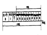
제1도는 이동 무선 자동차 전화기의 송신데이터 구성도.1 is a block diagram of transmission data of a mobile wireless vehicle telephone.
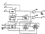
제2도는 본 발명의 이동 무선 자동차 전화기의 송신부의 블럭도.2 is a block diagram of a transmitting unit of a mobile radio telephone of the present invention.
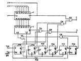
제3도는 제2도의 구체 회로도.3 is a concrete circuit diagram of FIG.
제4도는 제3도의 각 부분의 타이밍도.4 is a timing diagram of each part of FIG.
* 도면의 주요부분에 대한 부호의 설명* Explanation of symbols for main parts of the drawings
1 : 래치회로 2 : 시프트레지스터1: Latch Circuit 2: Shift Register
3 : 송신클럭동기회로 4 : 만체스터엔코오더3: transmission clock synchronous circuit 4: manchester encoder order
5 : 인테럽트 신호발생장치 6 : 병렬로드 신호발생장치5: interrupt signal generator 6: parallel load signal generator
본 발명은 이동 무선 자동차 전화기의 디지탈 데이터 통신용 송신부에 관한 것으로 특히 이동 무선 자동차 전화기의 디지탈 데이터 통신용 만체스터 엔코오더의 송신 광대역 데이터 출력 제어회로에 관한 것이다.BACKGROUND OF THE
현재 이동 무선 통신 시스템으로 셀루라 무선 통화방식이 사용되고 있다. 셀루라 무선 통화방식은 소정 지역을 셀(cell)이라는 다수의 통신구역으로 나누고 각각의 한 통신 구역마다 다른 주파수를 사용하며 또한 구역간의 간섭이 없는 다른 구역에서 사용한 주파수대를 다시 사용하여 주파수 이용 효율을 높이고 통화량을 증가시키며 통화품질을 높일수 있도록 한 방식이다. 미국은 셀루라 무선 통화방식으로 벨연구소가 개발한 AMPS(Advanced Mobile Phone Service) 시스넴과 AT & T사가 개발한 ARTS(American Radio Teliphone Service) 시스템이 운용되고 있다. 우리나라는 미국의 AMPS방식의 차량 무선전화 서어비스 업무를 1984년부터 개시해 왔다.Currently, cellular wireless communication is used as a mobile wireless communication system. Cellular wireless communication method divides a certain area into a plurality of communication areas called cells, uses different frequencies for each communication area, and reuses frequency bands used in other areas without interference between areas. It is to increase the call volume, increase the call volume and increase the call quality. In the US, Cellular wireless telephony is being operated by AMPS (Advanced Mobile Phone Service) system developed by Bell Labs and American Radio Teliphone Service (ARTS) system developed by AT & T. In 1984, Korea has begun AMPS-type wireless service service for vehicles.
AMPS시스템은 중앙통제국(MTSO)과 셀사이트(cell site)와 이동 무선 자동차 전화기로 구성된다. 중앙통제국과 셀 사이트 사이는 유선통신이 행해지고 셀 사이트와 이동 무선 자동차 전화기 사이에는 무선통신이 행해지고 있다. 중앙통제국(MTSO)은 일반 전화망과 AMPS시스템간의 상호 연결 및 셀 사이트에 할당된 채널을 관리 통제하며 요금계산 및 통화중 이동 무선 전화기를 합재한 자동차가 다른 통화지역 즉 다른 셀 사이트로 이동했을때 통화 단점등을 방지("Hand off"라 칭함)하는 기능을 한다. 셀사이트는 중앙통제국과 유선망 처리를 할수 있도록 신호를 변화시켜주며 항상 자기 셀 지역내에 있는 이동 무선 자동차 전화기의 신호 강도를 감시하여 중앙통제국에 정보를 제공해주고 중앙통제국에서 받은 정보를 이동 무선 자동차 전화기에게 전달해 준다. 그리하여 중앙통제국과 연결된 일반 가입자와 이동 무선 자동차 전화기간의 전화통화가 가능하게 된다.The AMPS system consists of a central control station (MTSO), a cell site and a mobile cordless car phone. Wired communication is performed between the central control station and the cell site, and wireless communication is performed between the cell site and the mobile radio telephone. The MTSO manages and controls the interconnection between the general telephone network and the AMPS system and the channels assigned to the cell sites. It is a function to prevent disadvantages ("Hand off"). CellSight changes the signal to handle the central control station and the wired network, always monitors the signal strength of the mobile cordless phone in its cell area, provides information to the central control station, and sends the information received from the central control station to the mobile cordless phone. Deliver it. Thus, a telephone call between a general subscriber connected to a central control station and a mobile wireless telephone can be made.
AMPS 시스템에서는 이동 무선 자동차 전화기에서 셀사이트로 보내는 송신 주파수대는 825-845MHZ의 20MHZ 대역폭을 갖고 있으며 이동 무선 자동차 전화기가 셀 사이트로 부터 받는 수신 주파수대는 870-890MHZ의 20MHZ 대역폭을 갖고 있다. 또한 각 송수신 주파수대는 30KHZ의 주파수 간격을 두어 666개의 채널을 갖고 있으며 양방향(full Duplex) 통신을 한다. 또한 각 주파수대에서 주파수 채널 333과 334채널을 중심으로 상하의 채널을 제어채널(총642채널)로 사용하고 나머지 312개의 상하 채널은 음성채널(총624채널)로 사용한다. 또한 AMPS 시스템에서 규정되어 사용되고 있는 이동 무선 자동차 전화기에서 셀 사이트 송신하는(reverse direction 이라함) 제어채널(setup channel 이라고 함)의 레이터 포맷과 음성채널의 데이터 포맷은 각각 제1(a)도 및 제1(b)도에 나타낸 바와 같다.In the AMPS system, the transmit frequency band sent from the mobile cordless phone to the cell site has a bandwidth of 20MHZ of 825-845MHZ and the receive band received from the cell site has a bandwidth of 20MHZ of 870-890MHZ. In addition, each transmit / receive frequency band has 666 channels with a frequency interval of 30KHZ, and performs full duplex communication. In each frequency band, the upper and lower channels are used as control channels (642 channels in total) around the frequency channels 333 and 334 channels, and the remaining 312 upper and lower channels are used as voice channels (624 channels in total). In addition, the data format of the voice channel and the format of the control channel (referred to as a reverse direction) and the voice channel of the cell site transmission (referred to as a reverse direction) in the mobile wireless mobile phone defined and used in the AMPS system are shown in FIGS. It is as showing in FIG. 1 (b).
제1(a)도에 도시한 제어채널의 데이터포맷의 1프레임은 비트동기용으로 사용되는 30비트의 도팅시컨스(Dotting sequence)와 데이터 동기용으로 사용되는 11비트의 워드싱크(word sync) 및 셀 사이트의 고유번호를 나타내는 7비트의 셀사이트 어드레스 데이터(cell Site ID)를 포함하고 있다. 또한 상기 셀 사이트 어드레스 데이터 다음에는 상기 상하 21채널의 제어채널에서 각각 사용되는 A시스템 제어데이터 A1-A5와 B시스템 제어데이터 B1-B5가 실리게 된다. 상기 제어데이터들은 각각 도시된 바와 같이 48비트로 되어 있다.One frame of the data format of the control channel shown in FIG. 1 (a) includes a 30-bit dotting sequence used for bit synchronization and an 11-bit word sync used for data synchronization; It contains 7-bit cell site ID data indicating a unique number of the cell site. Next to the cell site address data, A system control data A1-A5 and B system control data B1-B5 used in the control channels of the upper and lower 21 channels are loaded. The control data are each 48 bits as shown.
따라서 상기 제어 데이터들은 이동 무선 자동차 전화기에서 소정 셀 사이트와 발산(Access)시 제어채널에서 사용되는 등록, 식별, 확인에 사용하는 제어데이터들이 5번 반복된다.Therefore, the control data is repeated five times the control data used for the registration, identification, and confirmation used in the control channel when the mobile cell phone and the predetermined cell site and the access (Access).
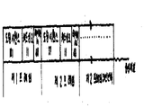
한편 제1(b)도에 도시한 음성채널의 데이터 포맷은 101비트의 도팅시퀀스와 11비트의 워드싱크 및 48비트의 데이터 A1으로 구성된 제 1 프레임과 37비트의 도팅시퀀스와 11비트의 워드싱크 및 48비트의 데이터 A2로 구성된 제 2프레임 및 상기 제 2프레임과 동일 데이터 포맷을 갖는 제 3 내지 제 5프레임이 상기 제 2프레임 뒤에 연속하여 연결되어 있는 구성을 갖는다. 음성채널의 데이터 포맷은 전술한 음성채널에서 상기 발신(Access)후에 사용되고 음성채널의 데이터는 셀 사이트 변경등의 이동 무선 자동차 전화기의 운용상태 모니터와 지시를 하는데 사용하는 5번 반복되는 데이터이다. 또한 AMPS 규정상 도팅스퀀스는 10101010...으로 사용하고 워드싱크는 11100010010으로 규정 사용하고 있다. 상기와 같은 데이터 포맷은 1980년에 발행된 IEEE Transaction on vehicular Technology, Vol 29, No.2 제238 내지 244페이지에 개재된바 있다.On the other hand, the data format of the voice channel shown in FIG. 1 (b) is a first frame consisting of a 101-bit dosing sequence, an 11-bit word sink, and a 48-bit data A1, a 37-bit dotting sequence, and an 11-bit word sink. And a second frame composed of 48 bits of data A2 and third to fifth frames having the same data format as the second frame are successively connected after the second frame. The data format of the voice channel is used after the access in the above-described voice channel, and the data of the voice channel is data repeated five times used to monitor and instruct the operation status of the mobile wireless mobile phone such as cell site change. Also, according to the AMPS regulations, the dotting sequence is set to 10101010 ... and the word sync is set to 11100010010. Such a data format is disclosed in IEEE Transaction on vehicular Technology, Vol 29, No. 2 pages 238 to 244 published in 1980.
한편 AMPS 시스템에서 사용하는 이동 무선 자동차 전화기의 시스템은 1979년 1월 벨연구소가 발행한 The Bell System Technical Journal, Vol 58, No.1의 제 123면 내지 제143면에 개시된바 있다. 그러나 본 발명은 여기에 개시된 시스템 모두와 관련되 있는것은 아니며, 송신과 관련된 데이터 엔코오더와 관련되 있음을 유의하여야 한다. 상기 벨연구소가 발행한 잡지 제138면 내지 제141면에 개재되 있는 바와 같이 AMPS 이동 무선 자동차 전화기에서의 제 1 도에 도시된 제어채널과 음성채널의 메세지들은 중앙처리장치(CPU)로 부터 NRZ(Nonreturn to Zero) 데이터로 출력되고 이 NPZ 데이터는 비트엔코오더 회로에 의해 10kbs의 광대역 송신데이터로 만체스터 엔코오딩이 된다. 통상적으로 중앙처리장치(CPU)는 8비튼 마이크로프로세서가 사용되어 왔다. 따라서 만체스터 엔코오더 회로는 상기 중앙처리장치에서 출력하는 8비트 데이터를 만체스터 엔코오딩을 해야하며 또한 시그날링톤을 송출해야 할시 즉 핸드오프(hand off)시 또는 홀드(hold)시 등에는 시그날링톤을 송출할수 있어야 하고 또한 중앙처리장치를 인테럽트시켜 주변장치의 프로그램을 수행할수 있는 인테럽트 신호를 출력하여야 한다. 또한 이동 무선 자동차 전화기는 자동차에 탑재하는 것이므로 소형, 경량, 저전력화가 요구되고 있다. 또한 이동 무선 자동차 전화기의 경우 주위의 환경 즉 온도, 진동 및 습도등의 조건이 상당히 넓은 범위에서 변화하는 경향이 있으므로 이러한 변동에 대해 신뢰성이 높고 오동작을 하지 않는 집적회로화 하는 것이 요망되고 있다.On the other hand, a system of a mobile cordless telephone for use in an AMPS system has been disclosed in pages 123 to 143 of The Bell System Technical Journal, Vol 58, No. 1, published by Bell Labs in January 1979. However, it should be noted that the present invention is not related to all of the systems disclosed herein, but rather to the data encoder associated with the transmission. The messages of the control channel and the voice channel shown in FIG. 1 in the AMPS mobile cordless telephone, as described in pages 138 to 141 of the magazine published by Bell Laboratories, are transmitted from the central processing unit (CPU) to the NRZ. It is output as (Nonreturn to Zero) data, and this NPZ data is manchester encoded as 10kbs wideband transmission data by a bit encoder circuit. Typically, a central processing unit (CPU) has been used an 8 bit microprocessor. Therefore, the Manchester encoder circuit needs to encode the 8-bit data output from the central processing unit, and the signaling tone when handing off or holding the signal when transmitting a signaling tone, ie, when handing off or holding. It should also be able to transmit the interrupt signal and interrupt signal to output the interrupt signal to program the peripheral device. In addition, mobile wireless telephones are mounted in automobiles, so they are required to be compact, lightweight, and low power. In addition, in the case of a mobile cordless mobile phone, the surrounding environment, that is, the conditions such as temperature, vibration, and humidity tend to change in a wide range, and it is desired to integrate an integrated circuit with high reliability and no malfunction.
따라서 본 발명의 목적은 이동 무선 자동차 전화기의 광대역 송신부를 모두 디지탈 논리회로로 구성하여 오동작 방지 및 높은 신뢰도를 제공할수 있는 엔코오더 회로를 제공함에 있다.Accordingly, an object of the present invention is to provide an encoder circuit capable of preventing malfunction and providing high reliability by constructing all of the wideband transmitters of a mobile wireless vehicle telephone with digital logic circuits.
본 발명의 또다른 목적은 집적회로화가 용이하여 소형, 경량, 저전력화 및 양산의 용이성을 제공할수 있는 엔코오더 회로를 제공함에 있다.It is still another object of the present invention to provide an encoder circuit that can be integrated circuitry and can provide small size, light weight, low power, and ease of mass production.
이하 본 발명을 도면을 참조하여 상세히 설명한다.Hereinafter, the present invention will be described in detail with reference to the drawings.
제 2 도는 본 발명에 따른 광대역 데이터 송신부인 엔코오더회로의 블럭도이다. 도면중 래치회로(1)는 도시하지 않은 전술한 CPU(중앙처리장치)로 부터 8비트씩 병렬로 출력하는 제 1 도의 각종데이터 메세지와 어드레스 디코오더 신호를 각각 데이터 입력단자(8)와 어드레스 입력단자(9)로 입력한다. 또한 데이터 또는 시그날링톤 제어신호 입력단자(7)를 부터 입력하는 제어신호에 따라 상기 CPU로 부터 출력하는 데이터 메세지를 병렬로 래치하는 기능을 한다. 즉 CPU로 부터 데이터를 출력할 시에는 상기 입력단자(7)로 데이터임을 알리는 논리신호를 입력하여 상기 래치회로(1)는 상기 입력한 병렬데이터를 래치시키고 시그날링톤을 출력해야 할 시에는 상기 래치회로(1)를 리세트 시킨다.2 is a block diagram of an encoder circuit which is a broadband data transmitter according to the present invention. In the drawing, the
시프트레지스터(2)는 클럭입력단자(11)로 입력하는 10KHZ의 클럭과 후술하는 병렬로드신호 발생장치(6)에서 출력하는 논리 제어신호에 따라 상기 래치회로(1)에서 래치된 병렬데이터를 병렬로 로드하고 이 병렬로 로드된 데이터를 직렬로 출력하는 기능을 한다.The
송신 클럭동기회로(3)는 클럭입력단자(11)로 입력하는 10KHZ의 클럭과 송신 인에이블 신호 입력단자(10)로 입력하는 CPU로 부터 출력하는 송신 인에이블 신호를 입력하여 송신클럭에 동기시키고 송신광대역 데이터를 송신하는 시간을 결정하는 신호를 출력단자(Q)에서 발생하며 송신 인에이블 신호의 입력이 없을때에는 병렬로드신호 발생장치(6)에 병렬 로드 신호를 출력하게 하는 신호를 발생한다.The transmit
인테럽트신호 발생장치(5)는 상기 송신광대역 데이터를 송신하는 시간을 결정하는 신로를 입력하여 세트되고 상기 클럭입력단자(11)로 입력하는 10KHZ클럭을 입력하여 카운트하므로써 데이터 송신시 CPU인테럽트 신호르 앤드게이트 G36과 함께 발생한다.The interrupt signal generator 5 is set by inputting a path for determining the time for transmitting the transmission wideband data, and counts by inputting and counting a 10KHZ clock input to the clock input terminal 11 to interrupt the CPU interrupt signal during data transmission. Occurs with Le Andgate G36.
병렬로드신호 발생장치(6)는 상기 인테럽트신호 발생장치(5)의 출력 및 10KHZ클럭과 상기 송신 클럭동기 회로(3)의 출력을 입력하여 송신 인에이블 신호 입력시 상기 시프트레지스터(2)에 로드된 병렬 데이터를 8비트마다 직렬 데이터로 출력하게 하고 송신 인에이블 신호의 입력이 없을시에는 상기 시프트레지스터(2)가 상기 래치회로(1)에 래치된 8비트 데이터를 병렬로 로드하게 하는 신호를 발생한다.The parallel load signal generator 6 inputs the output of the interrupt signal generator 5 and the output of the 10 KHZ clock and the transmit
또한 만체스터 엔코오더(4)는 상기 시프트레지스터(2)에서 출력하는 직렬데이타를 10KHZ클럭으로 만체스터 엔코오딩을 하여 만체스터 엔코오딩된 데이터를 출력한다.In addition, the Manchester encoder 4 outputs the Manchester encoded data by performing the Manchester encoding on the serial data output from the
앤드게이트 G36은 데이터 또는 시그날링톤 제어신호 입력단자(7)로 데이터 제어신호가 입력하고 송신 인에이블 신호가 입력할시 송신개시후 8비트의 데이터가 송출될때마다 인테럽트 신호를 출력단자(12)로 출력한다. 이 인테럽트신호는 CPU를 인테럽트 시켜 주변회로의 프로그램을 수행한다. 한편 앤드게이트 G33은 상기 제어신호 입력단자(7)로 시그날링톤 제어신호가 입력하며 10KHZ의 시그날링톤을 출력하고 상기 제어신호 입력단자(7)로 데이터 제어신호가 입력하고 송신 개시가 되면 광대역 송신데이터 출력단자(13)로 출력한다.The AND gate G36 outputs an interrupt signal whenever an 8-bit data is transmitted after the transmission start when the data control signal is input to the data or signaling tone control signal input terminal 7 and the transmit enable signal is input. Will output This interrupt signal interrupts the CPU to program peripheral circuits. Meanwhile, the AND gate G33 inputs a signaling tone control signal to the control signal input terminal 7, outputs a signaling tone of 10 KHZ, inputs a data control signal to the control signal input terminal 7, and starts transmission. Output to the
따라서 본 발명은 입력단자(7)로 데이터 입력 신호임을 알리는 "하이"(이하 "1"이라 함) 상태의 신호가 앤드게이트 G36으로 입력하고 송신 인에이블 신호가 입력단자(10)로 입력하며 10KHZ의 클럭신호가 송시 클럭동기회로(3)로 입력하며 송신 클럭동기회로(3)의 출력단자 Q는 "1"의 상태가 되며 출력단자![]()
![]()
따라서 앤드게이트 G33은 후출하는 만체스터 엔코오더(4)의 출력신호를 그대로 출력하게 된다.Therefore, the AND gate G33 outputs the output signal of the retracted Manchester encoder 4 as it is.
한편 인테럽트신호 발생장치(5)는 상기 송신 클럭동기회로(3)의 출력단자 Q의 출력신호인 "1"의 상태의 신호를 입력하며 상기 인테럽트신호발생장치(5)의 카운터를 세트시키고 10KHZ의 클럭신호를 입력 카운트하여 후술하는 만체스터 엔코우딩된 데이터의 7비트마다 100μsec의 인테럽트신호를 출력하여 상기 앤드게이트 G36을 통해 CPU를 인테럽트 시킨다. 한편 CPU의 데이터 출력단자로 부터 출력하는 8비트 병렬데이터는 래치회로(1)의 병렬데이터 입력단자(8)로 입력되어 어드레스 입력단자(9)에 입력되는 어드레스 신호에 따라 래치회로(1)에 래치가 된다.On the other hand, the interrupt signal generator 5 inputs a signal having a state of "1" which is an output signal of the output terminal Q of the transmission
또한 송신 클럭동기회로(3)의![]()
![]()
![]()
![]()
따라서 만체스터 엔코오도(4)는 상기 스프트레지스터(2)에서 출력하는 데이터 신호를 10KHZ 클럭에 따라 만체스터 엔코오딩을 하는데 상기 시프트레지스터(2)에서 출력하는 직렬 데이터를 50μsec 지연시켜 업에이지일때 "1"의 데이터를 나타내고 다운 에이지에서 "0"의 데이터가 나타나도록 100μsec마다 만체스터 엔코오딩된 신호가 만체스터 엔코오더(4)로 부터 출력하고 앤드게이트 G33을 통해 송신광대역 데이터 출력단자(13)로 출력하게 된다.Therefore, the Manchester encoder 4 performs the Manchester encoding of the data signal output from the
한편 이동 무선 자동차의 송신부는 데이터뿐만 아니라 스그날링톤(ST)도 전송할 수 있어야 하는데 이때에는 입력단자(7)를 "0"상태로 하여 래치회로(1)를 리세트시켜 데이터의 송출을 방지함과 동시에 CPU테럽트 신호으 송출을 앤드게이트 G36에 의해 중단시키고 인에이블신호(TINA)의 입력에 의한 송신 클럭동기회로(3)의 출력단자(Q)의 출력신호를 "1"로 하면 10KHZ 클럭에 의한 시그날링톤이 만체스터 엔코오더(4)를 통해 앤드게이트 G33으 출력단자로 출력하게 된다.On the other hand, the transmitting unit of the mobile wireless vehicle should be able to transmit not only data but also a slewing tone (ST). At this time, the input terminal 7 is set to "0" to reset the
한편 인에이블 신호의 입력이 없을시(예컨데 "0"상태)에는 송신 클럭동기회로(3)의 출력단자 Q는 "0"상태로 되어 앤드게이트 G33의 출력은 항상 "0"상태로 송신광대역 데이터의 송출은 없게 된다.On the other hand, when no enable signal is input (for example, "0" state), the output terminal Q of the transmission
제 3 도는 본 발명에 따른 제 2 도의 블럭도의 구체회로도의 일실시예로서 래치회로(1)와 시프트레지스터(2)와 D형 플립플롭 FF23 및 FF28과 T형 플립플롭 FF24-FF27 및 배타적 놀리합게이트(exclusive or gate)G32 및 G34와 오아게이트 G31 및 앤드게이트 G33, G35 및 G36와 인버어터 G37로 구성된다.3 is an embodiment of the specific circuit diagram of the block diagram of FIG. 2 according to the present invention, the
도면중 D형 플립플롭 FF23으로 구성된 부분이 제 2 도의 송신 클럭동기회로(3)이며 배타적 논리합게이트 G32로 구성된 부분이 만체스터 엔코오더(4)에 대응하며 T형 플립플롭 FF24-FF27 및 앤드케이트 G35로 구성된 부분이 인테럽트 신호 발생장치(5)에 대응하고 인버어터 G37과 D형 플립플롭 FF28과 배타적논리합게이트 G34 및 오아게이트 G31로 구성된 부분이 병렬로드 신호 발생장치(6)에 각각 대응한다.In the figure, the portion composed of the D flip-flop FF23 is the transmission
제 4 도는 본 발명에 따른 제 3 도의 구체회로도의 각 부분에 있어서의 타이밍도이다.4 is a timing diagram in each part of the concrete circuit diagram of FIG. 3 according to the present invention.
이하 제 3 도의 본 발명에 따른 구체회로도의 작동관계를 제 4 도의 타이밍도를 참조하여 상세히 설명한다.Hereinafter, the operation relationship of the concrete circuit diagram according to the present invention of FIG. 3 will be described in detail with reference to the timing diagram of FIG.
제 4 도의 송신 인에이블신호 TINA가 "0"상태일때 즉 데이터를 전송하지 않을때는 상기 신호가 송신 인에이블 입력단자(10)로 입력하여 10KHZ의 클럭신호가 클럭펄스 입력단스(11)로 입력하여 전술한 송신 클럭동기회로(3)로 작동하는 D형 플립플롭 FF23의 출력단자 Q23는 "0"가 출력하게 되며 반전 출력단자![]()
![]()
데이터 송신 필요시에는 데이터/시그날링톤 입력단자(7)에는 "1"상태의 신호가 입력하여 래치회로(1)는 세트 상태가 되며 데이터 입력단자(8)와 어드레스 신호 입력단자(9)에는 CPU로 부터 8비트 병렬데이터와 어드레스 신호가 입력하여 상기 데이터가 래치회로(1)에 병렬로 래치된다. 한편 송신 클럭동기회로(1)의 구성부분인 D형 플립플롭 FF23의 송신 인에이블 입력단자(10)에는 "1"상태의 송신 인에이블 신호가 입력하고 클럭입력단자(11)에는 10KHZ의 클럭펄스가 입력되고 10KHZ클럭에 동기되어 상기 D형 플립플롭 FF23의 출력단자 Q23에서는 제 4 도의 Q23클럭의 파형이 출력하게 된다.When data transmission is required, a signal of " 1 " state is inputted to the data / signaling tone input terminal 7, and the
따라서 송신 인에이블신호 TINA가 "1"상태가 유지되면 만체스터 엔코오더(4)가 되는 배타적 논리합게이트 G32의 출력신호가 앤드게이트 G33의 출력에 나타나 송신광대역 데이터 출력단자(13)으로 출력하게 된다.Therefore, when the transmit enable signal TINA is maintained at " 1 " state, the output signal of the exclusive logical sum gate G32, which becomes the Manchester encoder 4, appears at the output of the AND gate G33 and outputs to the transmission wideband
또한 상기 D형 플립플롭 FF23의 출력단자 Q23의 신호에 의해 인테럽트 신호발생장치(5)의 T형 플립플롭(FF24-FF27)으로 구성되는 카운터는 세트되고 상기 10KHZ클럭펄스가 카운트업 되며 상기 각 T형 플립플롭으리 출력단자Q24-Q27에는 제 4 도의 Q24 클럭 내지 Q2 클럭파형과 같이 출력이 되게된다.In addition, by the signal of the output terminal Q23 of the D-type flip-flop FF23, a counter composed of the T-type flip-flops (FF24-FF27) of the interrupt signal generator 5 is set, and the 10KHZ clock pulses are counted up. The output terminals Q24-Q27 of the T-type flip-flop are output like the Q24 clock to Q2 clock waveforms of FIG.
따라서 상기 카운터의 T형 플립플롭 FF27의 출력단자 Q27의 출력은 병렬로드신호 발생장치(6)내의 D형 플립플롭 FF28로 입력되며 상기 10KHZ의 클럭펄스가 인버어터 G37에 의해 인버어트된 후 상기 D형 플립플롭 FF28의 클럭펄스 입력단자로 입력하여 그 출력단자 Q28에서는 상기 카운터으 T형 플립플롭 FF27의 출력단자 Q27의 출력신호와 50μsec 뒤진신호(제 4 도 Q28클럭)가 출력하며 상기 양신호는 배타적 논리합게이트 G34에 입력하여 50μsec의 펄스폭을 갖는 펄스가 제 4 도의 G34의 출력파형과 같이 나타나고 오아게이트 G31의 출력은 송신 인에이블신호가 "0"상태일때와 사기 배타적 논리합게이트 G34의 출력이 "1"상태일때 "1"상태로 되게 되며 이 신호는 시프트레지스터(2)의 병렬, 직렬로드 신호입력단자![]()
![]()
![]()
![]()
따라서 제 4 도의 시프트레지스터 Q2 출력신호는 만체스터 엔코오더(4)가 되는 배타적 논리합게이트 G32에 상기 10KHZ 클럭펄스와 같이 입력하여 그 출력은 상기 시프트레지스터 Q2출력의 직렬데이터를 만체스터 엔코오딩(업에이지가 "1"이며 다운에이지가 "0"로 된 100μsec마다 1비트로 나타남)된 데이터가 출력하며 앤드게이트 G33을 통해 송신 광대역 데이터 출력단자(13)로 제 4 도의 G33출력파형과 같이 출력한다.Accordingly, the shift register Q2 output signal of FIG. 4 is inputted to the exclusive logical sum gate G32, which becomes the Manchester encoder 4, with the 10KHZ clock pulse, and the output of the shift register Q2 output is the Manchester encoding (up). Data is displayed as one bit every 100 μsec with the age of “1” and the down age of “0”), and is output as the G33 output waveform of FIG. 4 through the AND gate G33 to the transmission broadband
한편 인테럽트 신호발생장치(5)의 카운터중 T형 플립플롭 FF24-FF26의 출력단자 Q24, Q25, Q26의 출력신호는 앤드게이트 G35에 입력하여 송신 인에이블신호에 의해 D형 플립픕롭 FF23의 출력단자 Q23의 출력신호가 "1"이 된 상태에서 되는 앤드게이트 G33에서 출력하는 데이터가 7비트 출력한후 50μsec 후 약 100μsec의 시간을 갖고 "1"상태가 되는 인테럽트 신호를 앤드게이트 G36을 통해 CPU인테럽트 출력단자(12)로 출력한다.On the other hand, the output signals of the output terminals Q24, Q25 and Q26 of the T-type flip-flop FF24-FF26 among the counters of the interrupt signal generator 5 are inputted to the AND gate G35 to output the D-type flip-flop FF23 by the transmit enable signal. After an output of 7 bits of the output signal of the terminal Q23 with the output signal of "1", the interrupt signal which becomes the "1" state with the time of about 100 microseconds after 50 microseconds after 7-bit output is sent through the AND gate G36. Output to the CPU interrupt
한편 이동 무선 자동차 전화기의 경우 송신부는 데이터 이외에 시그날링톤(ST)도 전송할 수 있어야 하는데 이를 위해 CPU제어신호 데이터/시그날링톤을 두고 있다.On the other hand, in the case of a mobile wireless mobile phone, the transmitter should be able to transmit the signaling tone (ST) in addition to the data.
이 신호가 "0"이면 래치회로(1)는 리세트되고 앤드게이트 G36입력을 "0"으로 하기 때문에 인테럽트를 걸수 없게 되며 송신 인에이블신호를 "1"로 하면 10KHZ의 클럭이 만체스터 엔코오더(4)인 배타적 논리합게이트 G32에 입력하고 시프트레지스터의 출력단자 Q2는 "0"상태가 출력하므로 상기 10KHZ의 클럭이 배타적 논리합게이트 G32로 출력하며 앤드게이트 G33에도 상기 클럭이 출력하여 시그날링톤이 송신 광대역 데이터 출력단자(13)로 출력하게 된다.If this signal is " 0 ", the
상술한 바와 같이 본 발명은 전회로를 디지탈 논리회로화 하여 보다 정확한 데이터를 송출할 수 있고 신로도를 높이수 있으며 집적회로화 하여 소형, 경량 저전력화 및 생산공정의 단축으로 원가절감의 효과를 거둘수 있다.As described above, the present invention can digitalize the entire circuit to send more accurate data, increase the reliability, and integrate the integrated circuit to reduce the cost by reducing the size, light weight, and reducing the production process. have.
Claims (4)
Priority Applications (1)
| Application Number | Priority Date | Filing Date | Title |
|---|---|---|---|
| KR1019850007026A KR880000552B1 (en) | 1985-09-25 | 1985-09-25 | Data Transmission Circuit of Mobile Cordless Car Telephone |
Applications Claiming Priority (1)
| Application Number | Priority Date | Filing Date | Title |
|---|---|---|---|
| KR1019850007026A KR880000552B1 (en) | 1985-09-25 | 1985-09-25 | Data Transmission Circuit of Mobile Cordless Car Telephone |
Publications (2)
| Publication Number | Publication Date |
|---|---|
| KR870003636A KR870003636A (en) | 1987-04-18 |
| KR880000552B1 true KR880000552B1 (en) | 1988-04-13 |
Family
ID=19242876
Family Applications (1)
| Application Number | Title | Priority Date | Filing Date |
|---|---|---|---|
| KR1019850007026A Expired KR880000552B1 (en) | 1985-09-25 | 1985-09-25 | Data Transmission Circuit of Mobile Cordless Car Telephone |
Country Status (1)
| Country | Link |
|---|---|
| KR (1) | KR880000552B1 (en) |
-
1985
- 1985-09-25 KR KR1019850007026A patent/KR880000552B1/en not_active Expired
Also Published As
| Publication number | Publication date |
|---|---|
| KR870003636A (en) | 1987-04-18 |
Similar Documents
| Publication | Publication Date | Title |
|---|---|---|
| AU648003B2 (en) | Prioritized data transfer method and apparatus for a radiotelephone peripheral | |
| US5297142A (en) | Data transfer method and apparatus for communication between a peripheral and a master | |
| US3997727A (en) | Time division multiplexed digital switching apparatus | |
| US3862373A (en) | Adaptive sampling rate time division multiplexer and method | |
| IT1253991B (en) | METHOD OF MANAGEMENT OF RADIO-TELEPHONE MESSAGES ISSUED AT LOW POWER. | |
| JPH0887462A (en) | State machine and communication control method | |
| HU208204B (en) | Master and slave data transmission device, system and portable radiox telephone | |
| US4819230A (en) | Optimized bandwith allocation mechanism between circuit slots and packet bit stream in a communication network | |
| US5341370A (en) | Data transfer between high bit rate buses via unshielded low bit rate bus | |
| KR880000552B1 (en) | Data Transmission Circuit of Mobile Cordless Car Telephone | |
| US5894594A (en) | Voice announcement broadcasting technique for base station of CT-2 cordless telephone | |
| JPS61144935A (en) | Method and circuit apparatus for reducing protection time between time channels of degital type wireless communicationsystem | |
| AU682742B2 (en) | Co-ordinating access to a bus | |
| US6947765B1 (en) | Method for transmitting data between data processing means and a radio communication network, module and mobile terminal for implementing same | |
| JPH1075224A (en) | Telecommunication method | |
| EP0739573B1 (en) | Method and equipment for adapting ct2 calls for an isdn subscriber line | |
| KR0179211B1 (en) | Data strobe signal generation device for adjusting 48bps bit rate | |
| US20030096615A1 (en) | Signaling of a call in a telecommunications system between a base station and a mobile component | |
| KR0171964B1 (en) | Data strobe signal generator for 264bps bit rate adjustment | |
| KR0165001B1 (en) | Data strobe signal generating apparatus for controlling 252bps bitrate | |
| KR0141301B1 (en) | Phase-adjustable data clock signal generation circuit | |
| KR100198223B1 (en) | Time slot strove signal generating device for pcs | |
| JPH02256341A (en) | Synchronizing recovery circuit recovering word synchronization and radio communication equipment using the circuit | |
| KR100298289B1 (en) | Voice Inverter of Voice Mail System | |
| KR0141293B1 (en) | Data Clock Signal Generation Circuit |
Legal Events
| Date | Code | Title | Description |
|---|---|---|---|
| A201 | Request for examination | ||
| PA0109 | Patent application |
St.27 status event code: A-0-1-A10-A12-nap-PA0109 |
|
| PA0201 | Request for examination |
St.27 status event code: A-1-2-D10-D11-exm-PA0201 |
|
| R17-X000 | Change to representative recorded |
St.27 status event code: A-3-3-R10-R17-oth-X000 |
|
| PG1501 | Laying open of application |
St.27 status event code: A-1-1-Q10-Q12-nap-PG1501 |
|
| E902 | Notification of reason for refusal | ||
| PE0902 | Notice of grounds for rejection |
St.27 status event code: A-1-2-D10-D21-exm-PE0902 |
|
| T11-X000 | Administrative time limit extension requested |
St.27 status event code: U-3-3-T10-T11-oth-X000 |
|
| P11-X000 | Amendment of application requested |
St.27 status event code: A-2-2-P10-P11-nap-X000 |
|
| P13-X000 | Application amended |
St.27 status event code: A-2-2-P10-P13-nap-X000 |
|
| G160 | Decision to publish patent application | ||
| PG1605 | Publication of application before grant of patent |
St.27 status event code: A-2-2-Q10-Q13-nap-PG1605 |
|
| E701 | Decision to grant or registration of patent right | ||
| PE0701 | Decision of registration |
St.27 status event code: A-1-2-D10-D22-exm-PE0701 |
|
| GRNT | Written decision to grant | ||
| PR0701 | Registration of establishment |
St.27 status event code: A-2-4-F10-F11-exm-PR0701 |
|
| PR1002 | Payment of registration fee |
St.27 status event code: A-2-2-U10-U11-oth-PR1002 Fee payment year number: 1 |
|
| PR1001 | Payment of annual fee |
St.27 status event code: A-4-4-U10-U11-oth-PR1001 Fee payment year number: 4 |
|
| PR1001 | Payment of annual fee |
St.27 status event code: A-4-4-U10-U11-oth-PR1001 Fee payment year number: 5 |
|
| PR1001 | Payment of annual fee |
St.27 status event code: A-4-4-U10-U11-oth-PR1001 Fee payment year number: 6 |
|
| PR1001 | Payment of annual fee |
St.27 status event code: A-4-4-U10-U11-oth-PR1001 Fee payment year number: 7 |
|
| PR1001 | Payment of annual fee |
St.27 status event code: A-4-4-U10-U11-oth-PR1001 Fee payment year number: 8 |
|
| PR1001 | Payment of annual fee |
St.27 status event code: A-4-4-U10-U11-oth-PR1001 Fee payment year number: 9 |
|
| PR1001 | Payment of annual fee |
St.27 status event code: A-4-4-U10-U11-oth-PR1001 Fee payment year number: 10 |
|
| PR1001 | Payment of annual fee |
St.27 status event code: A-4-4-U10-U11-oth-PR1001 Fee payment year number: 11 |
|
| PR1001 | Payment of annual fee |
St.27 status event code: A-4-4-U10-U11-oth-PR1001 Fee payment year number: 12 |
|
| PR1001 | Payment of annual fee |
St.27 status event code: A-4-4-U10-U11-oth-PR1001 Fee payment year number: 13 |
|
| PR1001 | Payment of annual fee |
St.27 status event code: A-4-4-U10-U11-oth-PR1001 Fee payment year number: 14 |
|
| PR1001 | Payment of annual fee |
St.27 status event code: A-4-4-U10-U11-oth-PR1001 Fee payment year number: 15 |
|
| PR1001 | Payment of annual fee |
St.27 status event code: A-4-4-U10-U11-oth-PR1001 Fee payment year number: 16 |
|
| FPAY | Annual fee payment |
Payment date: 20040324 Year of fee payment: 17 |
|
| PR1001 | Payment of annual fee |
St.27 status event code: A-4-4-U10-U11-oth-PR1001 Fee payment year number: 17 |
|
| LAPS | Lapse due to unpaid annual fee | ||
| PC1903 | Unpaid annual fee |
St.27 status event code: A-4-4-U10-U13-oth-PC1903 Not in force date: 20050414 Payment event data comment text: Termination Category : DEFAULT_OF_REGISTRATION_FEE |
|
| PC1903 | Unpaid annual fee |
St.27 status event code: N-4-6-H10-H13-oth-PC1903 Ip right cessation event data comment text: Termination Category : DEFAULT_OF_REGISTRATION_FEE Not in force date: 20050414 |
|
| P22-X000 | Classification modified |
St.27 status event code: A-4-4-P10-P22-nap-X000 |
|
| P22-X000 | Classification modified |
St.27 status event code: A-4-4-P10-P22-nap-X000 |