KR20230061452A - 가스상 입자 감소를 위한 장치 및 방법들 - Google Patents
가스상 입자 감소를 위한 장치 및 방법들 Download PDFInfo
- Publication number
- KR20230061452A KR20230061452A KR1020237011001A KR20237011001A KR20230061452A KR 20230061452 A KR20230061452 A KR 20230061452A KR 1020237011001 A KR1020237011001 A KR 1020237011001A KR 20237011001 A KR20237011001 A KR 20237011001A KR 20230061452 A KR20230061452 A KR 20230061452A
- Authority
- KR
- South Korea
- Prior art keywords
- air flow
- flow apertures
- chamber lid
- chamber
- apertures
- Prior art date
- Legal status (The legal status is an assumption and is not a legal conclusion. Google has not performed a legal analysis and makes no representation as to the accuracy of the status listed.)
- Pending
Links
Images

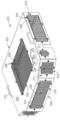
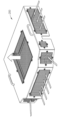
Classifications
-
- C—CHEMISTRY; METALLURGY
- C23—COATING METALLIC MATERIAL; COATING MATERIAL WITH METALLIC MATERIAL; CHEMICAL SURFACE TREATMENT; DIFFUSION TREATMENT OF METALLIC MATERIAL; COATING BY VACUUM EVAPORATION, BY SPUTTERING, BY ION IMPLANTATION OR BY CHEMICAL VAPOUR DEPOSITION, IN GENERAL; INHIBITING CORROSION OF METALLIC MATERIAL OR INCRUSTATION IN GENERAL
- C23C—COATING METALLIC MATERIAL; COATING MATERIAL WITH METALLIC MATERIAL; SURFACE TREATMENT OF METALLIC MATERIAL BY DIFFUSION INTO THE SURFACE, BY CHEMICAL CONVERSION OR SUBSTITUTION; COATING BY VACUUM EVAPORATION, BY SPUTTERING, BY ION IMPLANTATION OR BY CHEMICAL VAPOUR DEPOSITION, IN GENERAL
- C23C16/00—Chemical coating by decomposition of gaseous compounds, without leaving reaction products of surface material in the coating, i.e. chemical vapour deposition [CVD] processes
- C23C16/44—Chemical coating by decomposition of gaseous compounds, without leaving reaction products of surface material in the coating, i.e. chemical vapour deposition [CVD] processes characterised by the method of coating
- C23C16/4401—Means for minimising impurities, e.g. dust, moisture or residual gas, in the reaction chamber
-
- C—CHEMISTRY; METALLURGY
- C23—COATING METALLIC MATERIAL; COATING MATERIAL WITH METALLIC MATERIAL; CHEMICAL SURFACE TREATMENT; DIFFUSION TREATMENT OF METALLIC MATERIAL; COATING BY VACUUM EVAPORATION, BY SPUTTERING, BY ION IMPLANTATION OR BY CHEMICAL VAPOUR DEPOSITION, IN GENERAL; INHIBITING CORROSION OF METALLIC MATERIAL OR INCRUSTATION IN GENERAL
- C23C—COATING METALLIC MATERIAL; COATING MATERIAL WITH METALLIC MATERIAL; SURFACE TREATMENT OF METALLIC MATERIAL BY DIFFUSION INTO THE SURFACE, BY CHEMICAL CONVERSION OR SUBSTITUTION; COATING BY VACUUM EVAPORATION, BY SPUTTERING, BY ION IMPLANTATION OR BY CHEMICAL VAPOUR DEPOSITION, IN GENERAL
- C23C16/00—Chemical coating by decomposition of gaseous compounds, without leaving reaction products of surface material in the coating, i.e. chemical vapour deposition [CVD] processes
- C23C16/44—Chemical coating by decomposition of gaseous compounds, without leaving reaction products of surface material in the coating, i.e. chemical vapour deposition [CVD] processes characterised by the method of coating
- C23C16/52—Controlling or regulating the coating process
-
- H—ELECTRICITY
- H01—ELECTRIC ELEMENTS
- H01J—ELECTRIC DISCHARGE TUBES OR DISCHARGE LAMPS
- H01J37/00—Discharge tubes with provision for introducing objects or material to be exposed to the discharge, e.g. for the purpose of examination or processing thereof
- H01J37/32—Gas-filled discharge tubes
- H01J37/32431—Constructional details of the reactor
- H01J37/3244—Gas supply means
- H01J37/32449—Gas control, e.g. control of the gas flow
-
- H—ELECTRICITY
- H01—ELECTRIC ELEMENTS
- H01J—ELECTRIC DISCHARGE TUBES OR DISCHARGE LAMPS
- H01J37/00—Discharge tubes with provision for introducing objects or material to be exposed to the discharge, e.g. for the purpose of examination or processing thereof
- H01J37/32—Gas-filled discharge tubes
- H01J37/32431—Constructional details of the reactor
- H01J37/32458—Vessel
-
- H—ELECTRICITY
- H01—ELECTRIC ELEMENTS
- H01J—ELECTRIC DISCHARGE TUBES OR DISCHARGE LAMPS
- H01J37/00—Discharge tubes with provision for introducing objects or material to be exposed to the discharge, e.g. for the purpose of examination or processing thereof
- H01J37/32—Gas-filled discharge tubes
- H01J37/32431—Constructional details of the reactor
- H01J37/32458—Vessel
- H01J37/32522—Temperature
-
- H—ELECTRICITY
- H01—ELECTRIC ELEMENTS
- H01J—ELECTRIC DISCHARGE TUBES OR DISCHARGE LAMPS
- H01J37/00—Discharge tubes with provision for introducing objects or material to be exposed to the discharge, e.g. for the purpose of examination or processing thereof
- H01J37/32—Gas-filled discharge tubes
- H01J37/32431—Constructional details of the reactor
- H01J37/32798—Further details of plasma apparatus not provided for in groups H01J37/3244 - H01J37/32788; special provisions for cleaning or maintenance of the apparatus
- H01J37/32807—Construction (includes replacing parts of the apparatus)
-
- C—CHEMISTRY; METALLURGY
- C23—COATING METALLIC MATERIAL; COATING MATERIAL WITH METALLIC MATERIAL; CHEMICAL SURFACE TREATMENT; DIFFUSION TREATMENT OF METALLIC MATERIAL; COATING BY VACUUM EVAPORATION, BY SPUTTERING, BY ION IMPLANTATION OR BY CHEMICAL VAPOUR DEPOSITION, IN GENERAL; INHIBITING CORROSION OF METALLIC MATERIAL OR INCRUSTATION IN GENERAL
- C23C—COATING METALLIC MATERIAL; COATING MATERIAL WITH METALLIC MATERIAL; SURFACE TREATMENT OF METALLIC MATERIAL BY DIFFUSION INTO THE SURFACE, BY CHEMICAL CONVERSION OR SUBSTITUTION; COATING BY VACUUM EVAPORATION, BY SPUTTERING, BY ION IMPLANTATION OR BY CHEMICAL VAPOUR DEPOSITION, IN GENERAL
- C23C16/00—Chemical coating by decomposition of gaseous compounds, without leaving reaction products of surface material in the coating, i.e. chemical vapour deposition [CVD] processes
- C23C16/44—Chemical coating by decomposition of gaseous compounds, without leaving reaction products of surface material in the coating, i.e. chemical vapour deposition [CVD] processes characterised by the method of coating
- C23C16/4412—Details relating to the exhausts, e.g. pumps, filters, scrubbers, particle traps
Landscapes
- Chemical & Material Sciences (AREA)
- Engineering & Computer Science (AREA)
- Physics & Mathematics (AREA)
- Plasma & Fusion (AREA)
- Analytical Chemistry (AREA)
- Chemical Kinetics & Catalysis (AREA)
- General Chemical & Material Sciences (AREA)
- Materials Engineering (AREA)
- Mechanical Engineering (AREA)
- Metallurgy (AREA)
- Organic Chemistry (AREA)
- Chemical Vapour Deposition (AREA)
- Drying Of Semiconductors (AREA)
Applications Claiming Priority (3)
| Application Number | Priority Date | Filing Date | Title |
|---|---|---|---|
| US17/010,518 US20220064785A1 (en) | 2020-09-02 | 2020-09-02 | Apparatus and methods for gas phase particle reduction |
| US17/010,518 | 2020-09-02 | ||
| PCT/US2021/045077 WO2022051057A1 (en) | 2020-09-02 | 2021-08-06 | Apparatus and methods for gas phase particle reduction |
Publications (1)
| Publication Number | Publication Date |
|---|---|
| KR20230061452A true KR20230061452A (ko) | 2023-05-08 |
Family
ID=80358248
Family Applications (1)
| Application Number | Title | Priority Date | Filing Date |
|---|---|---|---|
| KR1020237011001A Pending KR20230061452A (ko) | 2020-09-02 | 2021-08-06 | 가스상 입자 감소를 위한 장치 및 방법들 |
Country Status (5)
| Country | Link |
|---|---|
| US (1) | US20220064785A1 (cg-RX-API-DMAC7.html) |
| JP (1) | JP7564338B2 (cg-RX-API-DMAC7.html) |
| KR (1) | KR20230061452A (cg-RX-API-DMAC7.html) |
| TW (1) | TWI920130B (cg-RX-API-DMAC7.html) |
| WO (1) | WO2022051057A1 (cg-RX-API-DMAC7.html) |
Family Cites Families (16)
| Publication number | Priority date | Publication date | Assignee | Title |
|---|---|---|---|---|
| JP4068175B2 (ja) * | 1996-06-12 | 2008-03-26 | 株式会社東芝 | プラズマ処理装置 |
| US6744020B2 (en) * | 2001-01-04 | 2004-06-01 | Tokyo Electron Limited | Heat processing apparatus |
| US20020100557A1 (en) * | 2001-01-29 | 2002-08-01 | Applied Materials, Inc. | ICP window heater integrated with faraday shield or floating electrode between the source power coil and the ICP window |
| US20050145341A1 (en) * | 2003-11-19 | 2005-07-07 | Masaki Suzuki | Plasma processing apparatus |
| JP4381963B2 (ja) | 2003-11-19 | 2009-12-09 | パナソニック株式会社 | プラズマ処理装置 |
| JP4943669B2 (ja) * | 2005-06-08 | 2012-05-30 | 東京エレクトロン株式会社 | 真空装置のシール構造 |
| US20100193510A1 (en) * | 2009-02-02 | 2010-08-05 | Danilychev Vladimir A | Wireless radiative system |
| JP5136574B2 (ja) * | 2009-05-01 | 2013-02-06 | 東京エレクトロン株式会社 | プラズマ処理装置及びプラズマ処理方法 |
| JP4887440B2 (ja) | 2010-04-20 | 2012-02-29 | シャープ株式会社 | プラズマ処理装置、プラズマ処理方法および半導体素子の製造方法 |
| KR101477292B1 (ko) * | 2012-12-20 | 2014-12-29 | 엘아이지에이디피 주식회사 | 기판 처리장치 |
| US9631417B2 (en) * | 2012-12-21 | 2017-04-25 | Milgard Manufacturing Incorporated | Screen corner attachment |
| US10249475B2 (en) * | 2014-04-01 | 2019-04-02 | Applied Materials, Inc. | Cooling mechanism utlized in a plasma reactor with enhanced temperature regulation |
| KR101565534B1 (ko) * | 2014-11-25 | 2015-11-13 | 주식회사 원익아이피에스 | 진공처리장치 |
| US20180142355A1 (en) * | 2016-11-18 | 2018-05-24 | Adnanotek Corp. | System integrating atomic layer deposition and reactive ion etching |
| KR20190071520A (ko) * | 2017-12-14 | 2019-06-24 | 이재섭 | 윈도우 히팅 시스템 |
| US11152207B2 (en) * | 2018-07-26 | 2021-10-19 | Tokyo Electron Limited | Method of forming titanium nitride films with (200) crystallographic texture |
-
2020
- 2020-09-02 US US17/010,518 patent/US20220064785A1/en not_active Abandoned
-
2021
- 2021-08-06 KR KR1020237011001A patent/KR20230061452A/ko active Pending
- 2021-08-06 WO PCT/US2021/045077 patent/WO2022051057A1/en not_active Ceased
- 2021-08-06 JP JP2023513279A patent/JP7564338B2/ja active Active
- 2021-09-02 TW TW110132621A patent/TWI920130B/zh active
Also Published As
| Publication number | Publication date |
|---|---|
| WO2022051057A1 (en) | 2022-03-10 |
| JP7564338B2 (ja) | 2024-10-08 |
| TW202242171A (zh) | 2022-11-01 |
| US20220064785A1 (en) | 2022-03-03 |
| JP2023539241A (ja) | 2023-09-13 |
| TWI920130B (zh) | 2026-04-01 |
Similar Documents
| Publication | Publication Date | Title |
|---|---|---|
| KR101201964B1 (ko) | 에피택셜 증착 프로세스 및 장치 | |
| JP7046162B2 (ja) | 高選択性酸化物除去および高温汚染物質除去と統合されたエピタキシシステム | |
| US4745088A (en) | Vapor phase growth on semiconductor wafers | |
| JP2020532114A (ja) | 一体型エピタキシシステム高温汚染物質除去 | |
| TW202338149A (zh) | 基材製程裝置及方法 | |
| US20120076936A1 (en) | Substrate processing apparatus, gas nozzle and method of processing substrate | |
| JPH02138473A (ja) | 縦型熱処理装置 | |
| US10679827B2 (en) | Method and apparatus for semiconductor processing chamber isolation for reduced particles and improved uniformity | |
| US20170350038A1 (en) | Vacuum platform with process chambers for removing carbon contaminants and surface oxide from semiconductor substrates | |
| KR102814336B1 (ko) | 기판 처리 장치, 기판 처리 방법 및 프로그램 | |
| CN107636816A (zh) | 对生长外延晶片的反应器的重操作进行准备的方法 | |
| JP2012023073A (ja) | 基板処理装置および基板の製造方法 | |
| US20040178176A1 (en) | Apparatus and method for cleaning a bell jar in a barrel epitaxial reactor | |
| TW201923137A (zh) | 用於磊晶沉積製程之注入組件 | |
| US20110217852A1 (en) | Substrate processing apparatus and method of manufacturing semiconductor device | |
| TWI920130B (zh) | 用於氣相顆粒減少的腔室蓋以及處理基板的方法 | |
| JP2019517736A (ja) | 半導体基板から炭素汚染物質及び表面酸化物を除去するための処理チャンバを有する真空プラットフォーム | |
| KR102034901B1 (ko) | 공정 챔버의 세정 방법 | |
| JP6450851B2 (ja) | エピタキシャルウェーハの成長のためのリアクターの再稼動準備方法 | |
| US20220275505A1 (en) | High throughput and metal contamination control oven for chamber component cleaning process | |
| CN113604875B (zh) | 一种气相外延系统及其维护操作方法 | |
| WO2017209900A1 (en) | A vacuum platform with process chambers for removing carbon contaminants and surface oxide from semiconductor substrates |
Legal Events
| Date | Code | Title | Description |
|---|---|---|---|
| PA0105 | International application |
St.27 status event code: A-0-1-A10-A15-nap-PA0105 |
|
| PG1501 | Laying open of application |
St.27 status event code: A-1-1-Q10-Q12-nap-PG1501 |
|
| R17-X000 | Change to representative recorded |
St.27 status event code: A-3-3-R10-R17-oth-X000 |
|
| A201 | Request for examination | ||
| PA0201 | Request for examination |
St.27 status event code: A-1-2-D10-D11-exm-PA0201 |
|
| D21 | Rejection of application intended |
Free format text: ST27 STATUS EVENT CODE: A-1-2-D10-D21-EXM-PE0902 (AS PROVIDED BY THE NATIONAL OFFICE) |
|
| PE0902 | Notice of grounds for rejection |
St.27 status event code: A-1-2-D10-D21-exm-PE0902 |
|
| P11 | Amendment of application requested |
Free format text: ST27 STATUS EVENT CODE: A-2-2-P10-P11-NAP-X000 (AS PROVIDED BY THE NATIONAL OFFICE) |
|
| P11-X000 | Amendment of application requested |
St.27 status event code: A-2-2-P10-P11-nap-X000 |
|
| P13 | Application amended |
Free format text: ST27 STATUS EVENT CODE: A-2-2-P10-P13-NAP-X000 (AS PROVIDED BY THE NATIONAL OFFICE) |
|
| P13-X000 | Application amended |
St.27 status event code: A-2-2-P10-P13-nap-X000 |