KR20220155893A - 다이 고정을 위한 하이브리드 본딩 방법 - Google Patents
다이 고정을 위한 하이브리드 본딩 방법 Download PDFInfo
- Publication number
- KR20220155893A KR20220155893A KR1020220009754A KR20220009754A KR20220155893A KR 20220155893 A KR20220155893 A KR 20220155893A KR 1020220009754 A KR1020220009754 A KR 1020220009754A KR 20220009754 A KR20220009754 A KR 20220009754A KR 20220155893 A KR20220155893 A KR 20220155893A
- Authority
- KR
- South Korea
- Prior art keywords
- dies
- die
- carrier
- target blocks
- carrier film
- Prior art date
- Legal status (The legal status is an assumption and is not a legal conclusion. Google has not performed a legal analysis and makes no representation as to the accuracy of the status listed.)
- Granted
Links
- 238000000034 method Methods 0.000 title claims abstract description 102
- 239000000758 substrate Substances 0.000 claims abstract description 48
- 239000010419 fine particle Substances 0.000 claims abstract description 39
- 238000005520 cutting process Methods 0.000 claims abstract description 20
- 229910000679 solder Inorganic materials 0.000 claims abstract description 10
- 238000000926 separation method Methods 0.000 claims description 13
- 230000000994 depressogenic effect Effects 0.000 claims description 6
- 238000010438 heat treatment Methods 0.000 claims description 4
- 230000001678 irradiating effect Effects 0.000 claims description 2
- 230000000694 effects Effects 0.000 abstract description 7
- 238000010586 diagram Methods 0.000 description 21
- 235000012431 wafers Nutrition 0.000 description 16
- 239000007788 liquid Substances 0.000 description 11
- 238000005498 polishing Methods 0.000 description 10
- 238000001179 sorption measurement Methods 0.000 description 7
- 239000000126 substance Substances 0.000 description 7
- 239000000203 mixture Substances 0.000 description 6
- RYGMFSIKBFXOCR-UHFFFAOYSA-N Copper Chemical compound [Cu] RYGMFSIKBFXOCR-UHFFFAOYSA-N 0.000 description 4
- 229910052802 copper Inorganic materials 0.000 description 4
- 239000010949 copper Substances 0.000 description 4
- 239000007921 spray Substances 0.000 description 3
- 229910003460 diamond Inorganic materials 0.000 description 2
- 239000010432 diamond Substances 0.000 description 2
- 238000005516 engineering process Methods 0.000 description 2
- 239000000463 material Substances 0.000 description 2
- 238000007517 polishing process Methods 0.000 description 2
- 239000004065 semiconductor Substances 0.000 description 2
- 230000003746 surface roughness Effects 0.000 description 2
- 230000004913 activation Effects 0.000 description 1
- 230000015572 biosynthetic process Effects 0.000 description 1
- 238000004140 cleaning Methods 0.000 description 1
- 238000004519 manufacturing process Methods 0.000 description 1
- 238000012986 modification Methods 0.000 description 1
- 230000004048 modification Effects 0.000 description 1
- 238000004806 packaging method and process Methods 0.000 description 1
- 230000002093 peripheral effect Effects 0.000 description 1
- 239000011800 void material Substances 0.000 description 1
Images


Classifications
-
- H—ELECTRICITY
- H01—ELECTRIC ELEMENTS
- H01L—SEMICONDUCTOR DEVICES NOT COVERED BY CLASS H10
- H01L21/00—Processes or apparatus adapted for the manufacture or treatment of semiconductor or solid state devices or of parts thereof
- H01L21/02—Manufacture or treatment of semiconductor devices or of parts thereof
- H01L21/04—Manufacture or treatment of semiconductor devices or of parts thereof the devices having potential barriers, e.g. a PN junction, depletion layer or carrier concentration layer
- H01L21/50—Assembly of semiconductor devices using processes or apparatus not provided for in a single one of the groups H01L21/18 - H01L21/326 or H10D48/04 - H10D48/07 e.g. sealing of a cap to a base of a container
- H01L21/52—Mounting semiconductor bodies in containers
-
- H—ELECTRICITY
- H01—ELECTRIC ELEMENTS
- H01L—SEMICONDUCTOR DEVICES NOT COVERED BY CLASS H10
- H01L21/00—Processes or apparatus adapted for the manufacture or treatment of semiconductor or solid state devices or of parts thereof
- H01L21/02—Manufacture or treatment of semiconductor devices or of parts thereof
- H01L21/02041—Cleaning
- H01L21/02076—Cleaning after the substrates have been singulated
-
- H—ELECTRICITY
- H01—ELECTRIC ELEMENTS
- H01L—SEMICONDUCTOR DEVICES NOT COVERED BY CLASS H10
- H01L21/00—Processes or apparatus adapted for the manufacture or treatment of semiconductor or solid state devices or of parts thereof
- H01L21/67—Apparatus specially adapted for handling semiconductor or electric solid state devices during manufacture or treatment thereof; Apparatus specially adapted for handling wafers during manufacture or treatment of semiconductor or electric solid state devices or components ; Apparatus not specifically provided for elsewhere
- H01L21/67005—Apparatus not specifically provided for elsewhere
- H01L21/67011—Apparatus for manufacture or treatment
- H01L21/67092—Apparatus for mechanical treatment
-
- H—ELECTRICITY
- H01—ELECTRIC ELEMENTS
- H01L—SEMICONDUCTOR DEVICES NOT COVERED BY CLASS H10
- H01L21/00—Processes or apparatus adapted for the manufacture or treatment of semiconductor or solid state devices or of parts thereof
- H01L21/67—Apparatus specially adapted for handling semiconductor or electric solid state devices during manufacture or treatment thereof; Apparatus specially adapted for handling wafers during manufacture or treatment of semiconductor or electric solid state devices or components ; Apparatus not specifically provided for elsewhere
- H01L21/67005—Apparatus not specifically provided for elsewhere
- H01L21/67011—Apparatus for manufacture or treatment
- H01L21/67132—Apparatus for placing on an insulating substrate, e.g. tape
-
- H—ELECTRICITY
- H01—ELECTRIC ELEMENTS
- H01L—SEMICONDUCTOR DEVICES NOT COVERED BY CLASS H10
- H01L21/00—Processes or apparatus adapted for the manufacture or treatment of semiconductor or solid state devices or of parts thereof
- H01L21/67—Apparatus specially adapted for handling semiconductor or electric solid state devices during manufacture or treatment thereof; Apparatus specially adapted for handling wafers during manufacture or treatment of semiconductor or electric solid state devices or components ; Apparatus not specifically provided for elsewhere
- H01L21/683—Apparatus specially adapted for handling semiconductor or electric solid state devices during manufacture or treatment thereof; Apparatus specially adapted for handling wafers during manufacture or treatment of semiconductor or electric solid state devices or components ; Apparatus not specifically provided for elsewhere for supporting or gripping
- H01L21/6835—Apparatus specially adapted for handling semiconductor or electric solid state devices during manufacture or treatment thereof; Apparatus specially adapted for handling wafers during manufacture or treatment of semiconductor or electric solid state devices or components ; Apparatus not specifically provided for elsewhere for supporting or gripping using temporarily an auxiliary support
- H01L21/6836—Wafer tapes, e.g. grinding or dicing support tapes
-
- H—ELECTRICITY
- H01—ELECTRIC ELEMENTS
- H01L—SEMICONDUCTOR DEVICES NOT COVERED BY CLASS H10
- H01L21/00—Processes or apparatus adapted for the manufacture or treatment of semiconductor or solid state devices or of parts thereof
- H01L21/70—Manufacture or treatment of devices consisting of a plurality of solid state components formed in or on a common substrate or of parts thereof; Manufacture of integrated circuit devices or of parts thereof
- H01L21/77—Manufacture or treatment of devices consisting of a plurality of solid state components or integrated circuits formed in, or on, a common substrate
- H01L21/78—Manufacture or treatment of devices consisting of a plurality of solid state components or integrated circuits formed in, or on, a common substrate with subsequent division of the substrate into plural individual devices
-
- H—ELECTRICITY
- H10—SEMICONDUCTOR DEVICES; ELECTRIC SOLID-STATE DEVICES NOT OTHERWISE PROVIDED FOR
- H10D—INORGANIC ELECTRIC SEMICONDUCTOR DEVICES
- H10D84/00—Integrated devices formed in or on semiconductor substrates that comprise only semiconducting layers, e.g. on Si wafers or on GaAs-on-Si wafers
- H10D84/01—Manufacture or treatment
-
- H—ELECTRICITY
- H01—ELECTRIC ELEMENTS
- H01L—SEMICONDUCTOR DEVICES NOT COVERED BY CLASS H10
- H01L21/00—Processes or apparatus adapted for the manufacture or treatment of semiconductor or solid state devices or of parts thereof
- H01L21/67—Apparatus specially adapted for handling semiconductor or electric solid state devices during manufacture or treatment thereof; Apparatus specially adapted for handling wafers during manufacture or treatment of semiconductor or electric solid state devices or components ; Apparatus not specifically provided for elsewhere
- H01L21/67005—Apparatus not specifically provided for elsewhere
- H01L21/67011—Apparatus for manufacture or treatment
- H01L21/67098—Apparatus for thermal treatment
- H01L21/67115—Apparatus for thermal treatment mainly by radiation
-
- H—ELECTRICITY
- H01—ELECTRIC ELEMENTS
- H01L—SEMICONDUCTOR DEVICES NOT COVERED BY CLASS H10
- H01L21/00—Processes or apparatus adapted for the manufacture or treatment of semiconductor or solid state devices or of parts thereof
- H01L21/67—Apparatus specially adapted for handling semiconductor or electric solid state devices during manufacture or treatment thereof; Apparatus specially adapted for handling wafers during manufacture or treatment of semiconductor or electric solid state devices or components ; Apparatus not specifically provided for elsewhere
- H01L21/683—Apparatus specially adapted for handling semiconductor or electric solid state devices during manufacture or treatment thereof; Apparatus specially adapted for handling wafers during manufacture or treatment of semiconductor or electric solid state devices or components ; Apparatus not specifically provided for elsewhere for supporting or gripping
- H01L21/6838—Apparatus specially adapted for handling semiconductor or electric solid state devices during manufacture or treatment thereof; Apparatus specially adapted for handling wafers during manufacture or treatment of semiconductor or electric solid state devices or components ; Apparatus not specifically provided for elsewhere for supporting or gripping with gripping and holding devices using a vacuum; Bernoulli devices
-
- H—ELECTRICITY
- H01—ELECTRIC ELEMENTS
- H01L—SEMICONDUCTOR DEVICES NOT COVERED BY CLASS H10
- H01L2221/00—Processes or apparatus adapted for the manufacture or treatment of semiconductor or solid state devices or of parts thereof covered by H01L21/00
- H01L2221/67—Apparatus for handling semiconductor or electric solid state devices during manufacture or treatment thereof; Apparatus for handling wafers during manufacture or treatment of semiconductor or electric solid state devices or components; Apparatus not specifically provided for elsewhere
- H01L2221/683—Apparatus for handling semiconductor or electric solid state devices during manufacture or treatment thereof; Apparatus for handling wafers during manufacture or treatment of semiconductor or electric solid state devices or components; Apparatus not specifically provided for elsewhere for supporting or gripping
- H01L2221/68304—Apparatus for handling semiconductor or electric solid state devices during manufacture or treatment thereof; Apparatus for handling wafers during manufacture or treatment of semiconductor or electric solid state devices or components; Apparatus not specifically provided for elsewhere for supporting or gripping using temporarily an auxiliary support
- H01L2221/68318—Auxiliary support including means facilitating the separation of a device or wafer from the auxiliary support
- H01L2221/68322—Auxiliary support including means facilitating the selective separation of some of a plurality of devices from the auxiliary support
-
- H—ELECTRICITY
- H01—ELECTRIC ELEMENTS
- H01L—SEMICONDUCTOR DEVICES NOT COVERED BY CLASS H10
- H01L2221/00—Processes or apparatus adapted for the manufacture or treatment of semiconductor or solid state devices or of parts thereof covered by H01L21/00
- H01L2221/67—Apparatus for handling semiconductor or electric solid state devices during manufacture or treatment thereof; Apparatus for handling wafers during manufacture or treatment of semiconductor or electric solid state devices or components; Apparatus not specifically provided for elsewhere
- H01L2221/683—Apparatus for handling semiconductor or electric solid state devices during manufacture or treatment thereof; Apparatus for handling wafers during manufacture or treatment of semiconductor or electric solid state devices or components; Apparatus not specifically provided for elsewhere for supporting or gripping
- H01L2221/68304—Apparatus for handling semiconductor or electric solid state devices during manufacture or treatment thereof; Apparatus for handling wafers during manufacture or treatment of semiconductor or electric solid state devices or components; Apparatus not specifically provided for elsewhere for supporting or gripping using temporarily an auxiliary support
- H01L2221/68327—Apparatus for handling semiconductor or electric solid state devices during manufacture or treatment thereof; Apparatus for handling wafers during manufacture or treatment of semiconductor or electric solid state devices or components; Apparatus not specifically provided for elsewhere for supporting or gripping using temporarily an auxiliary support used during dicing or grinding
- H01L2221/68331—Apparatus for handling semiconductor or electric solid state devices during manufacture or treatment thereof; Apparatus for handling wafers during manufacture or treatment of semiconductor or electric solid state devices or components; Apparatus not specifically provided for elsewhere for supporting or gripping using temporarily an auxiliary support used during dicing or grinding of passive members, e.g. die mounting substrate
-
- H—ELECTRICITY
- H01—ELECTRIC ELEMENTS
- H01L—SEMICONDUCTOR DEVICES NOT COVERED BY CLASS H10
- H01L2221/00—Processes or apparatus adapted for the manufacture or treatment of semiconductor or solid state devices or of parts thereof covered by H01L21/00
- H01L2221/67—Apparatus for handling semiconductor or electric solid state devices during manufacture or treatment thereof; Apparatus for handling wafers during manufacture or treatment of semiconductor or electric solid state devices or components; Apparatus not specifically provided for elsewhere
- H01L2221/683—Apparatus for handling semiconductor or electric solid state devices during manufacture or treatment thereof; Apparatus for handling wafers during manufacture or treatment of semiconductor or electric solid state devices or components; Apparatus not specifically provided for elsewhere for supporting or gripping
- H01L2221/68304—Apparatus for handling semiconductor or electric solid state devices during manufacture or treatment thereof; Apparatus for handling wafers during manufacture or treatment of semiconductor or electric solid state devices or components; Apparatus not specifically provided for elsewhere for supporting or gripping using temporarily an auxiliary support
- H01L2221/68363—Apparatus for handling semiconductor or electric solid state devices during manufacture or treatment thereof; Apparatus for handling wafers during manufacture or treatment of semiconductor or electric solid state devices or components; Apparatus not specifically provided for elsewhere for supporting or gripping using temporarily an auxiliary support used in a transfer process involving transfer directly from an origin substrate to a target substrate without use of an intermediate handle substrate
-
- H—ELECTRICITY
- H01—ELECTRIC ELEMENTS
- H01L—SEMICONDUCTOR DEVICES NOT COVERED BY CLASS H10
- H01L2221/00—Processes or apparatus adapted for the manufacture or treatment of semiconductor or solid state devices or of parts thereof covered by H01L21/00
- H01L2221/67—Apparatus for handling semiconductor or electric solid state devices during manufacture or treatment thereof; Apparatus for handling wafers during manufacture or treatment of semiconductor or electric solid state devices or components; Apparatus not specifically provided for elsewhere
- H01L2221/683—Apparatus for handling semiconductor or electric solid state devices during manufacture or treatment thereof; Apparatus for handling wafers during manufacture or treatment of semiconductor or electric solid state devices or components; Apparatus not specifically provided for elsewhere for supporting or gripping
- H01L2221/68304—Apparatus for handling semiconductor or electric solid state devices during manufacture or treatment thereof; Apparatus for handling wafers during manufacture or treatment of semiconductor or electric solid state devices or components; Apparatus not specifically provided for elsewhere for supporting or gripping using temporarily an auxiliary support
- H01L2221/68368—Apparatus for handling semiconductor or electric solid state devices during manufacture or treatment thereof; Apparatus for handling wafers during manufacture or treatment of semiconductor or electric solid state devices or components; Apparatus not specifically provided for elsewhere for supporting or gripping using temporarily an auxiliary support used in a transfer process involving at least two transfer steps, i.e. including an intermediate handle substrate
-
- H—ELECTRICITY
- H01—ELECTRIC ELEMENTS
- H01L—SEMICONDUCTOR DEVICES NOT COVERED BY CLASS H10
- H01L2221/00—Processes or apparatus adapted for the manufacture or treatment of semiconductor or solid state devices or of parts thereof covered by H01L21/00
- H01L2221/67—Apparatus for handling semiconductor or electric solid state devices during manufacture or treatment thereof; Apparatus for handling wafers during manufacture or treatment of semiconductor or electric solid state devices or components; Apparatus not specifically provided for elsewhere
- H01L2221/683—Apparatus for handling semiconductor or electric solid state devices during manufacture or treatment thereof; Apparatus for handling wafers during manufacture or treatment of semiconductor or electric solid state devices or components; Apparatus not specifically provided for elsewhere for supporting or gripping
- H01L2221/68304—Apparatus for handling semiconductor or electric solid state devices during manufacture or treatment thereof; Apparatus for handling wafers during manufacture or treatment of semiconductor or electric solid state devices or components; Apparatus not specifically provided for elsewhere for supporting or gripping using temporarily an auxiliary support
- H01L2221/68381—Details of chemical or physical process used for separating the auxiliary support from a device or wafer
- H01L2221/68386—Separation by peeling
- H01L2221/6839—Separation by peeling using peeling wedge or knife or bar
Landscapes
- Engineering & Computer Science (AREA)
- Physics & Mathematics (AREA)
- Condensed Matter Physics & Semiconductors (AREA)
- General Physics & Mathematics (AREA)
- Manufacturing & Machinery (AREA)
- Computer Hardware Design (AREA)
- Microelectronics & Electronic Packaging (AREA)
- Power Engineering (AREA)
- Container, Conveyance, Adherence, Positioning, Of Wafer (AREA)
- Die Bonding (AREA)
- Dicing (AREA)
Abstract
Description
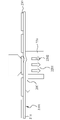
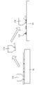
도 2는 두 번째 종래 기술에 따른 다이 박리 방법의 모식도이다.
도 3은 본 발명에 따른 다이 고정을 위한 하이브리드 본딩 방법의 흐름도이다.
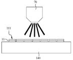
도 4는 본 발명에 따른 다이 고정을 위한 하이브리드 본딩 방법의 단계 S100의 화학적 기계 연마 공정의 모식도이다.
도 5a는 본 발명에 따른 다이 고정을 위한 하이브리드 본딩 방법의 단계 S100의 기계적 절단 공정의 평면도이다.
도 5b는 본 발명에 따른 다이 고정을 위한 하이브리드 본딩 방법의 단계 S100B의 기계적 절단 공정의 모식도이다.
도 6a는 본 발명에 따른 다이 고정을 위한 하이브리드 본딩 방법의 단계 S100의 절단이 완료된 상태의 평면도이다.
도 6b는 본 발명에 따른 다이 고정을 위한 하이브리드 본딩 방법의 단계 S100의 절단이 완료된 상태의 모식도이다.
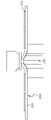
도 7은 본 발명에 따른 다이 고정을 위한 하이브리드 본딩 방법의 단계 S200의 모식도이다.
도 8은 본 발명에 따른 다이 고정을 위한 하이브리드 본딩 방법의 단계 S300의 모식도이다.
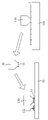
도 9a는 본 발명에 따른 다이 고정을 위한 하이브리드 본딩 방법의 단계 S400의 첫 번째 사전 코너 박리 방식을 보인 사시도이다.
도 9b는 본 발명에 따른 다이 고정을 위한 하이브리드 본딩 방법의 단계 S400의 첫 번째 사전 코너 박리 방식을 보인 평면도이다.
도 9c는 도 9b의 A-A 선을 따라 절개된 상태의 단면도이다.
도 10a는 본 발명에 따른 다이 고정을 위한 하이브리드 본딩 방법의 단계 S400의 두 번째 사전 코너 박리 방식을 보인 사시도이다.
도 10b는 본 발명에 따른 다이 고정을 위한 하이브리드 본딩 방법의 단계 S400의 두 번째 사전 코너 박리 방식을 보인 평면도이다.
도 10c는 도 10b의 B-B 선을 따라 절개된 상태의 단면도이다.
도 11a는 본 발명에 따른 다이 고정을 위한 하이브리드 본딩 방법의 단계 S400의 세 번째 사전 코너 박리 방식을 보인 사시도이다.
도 11b는 본 발명에 따른 다이 고정을 위한 하이브리드 본딩 방법의 단계 S400의 세 번째 사전 코너 박리 방식을 보인 평면도이다.
도 11c는 도 11b의 C-C 선을 따라 절개된 상태의 단면도이다.
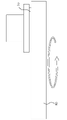
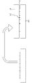
도 12는 본 발명에 따른 다이 고정을 위한 하이브리드 본딩 방법의 단계 S500의 모식도이다.
도 13은 본 발명에 따른 다이 고정을 위한 하이브리드 본딩 방법의 단계 S600의 모식도이다.
도 14는 본 발명에 따른 다이 고정을 위한 하이브리드 본딩 방법의 단계 S700의 모식도이다.
도 15는 본 발명에 따른 다이 고정을 위한 하이브리드 본딩 방법의 단계 S800의 첫 번째 다이 이송 방식을 보인 모식도이다.
도 16 내지 도 18은 본 발명에 따른 다이 고정을 위한 하이브리드 본딩 방법의 단계 S800의 두 번째 다이 이송 방식을 보인 모식도이다.
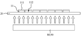
11: 다이
111: 제1 표면
112: 제2 표면
12: 미세 입자
13: 절단 라인
14: 다이 조합
20: 캐리어 필름
21: 타깃 블록
22: 타깃 블록 조합
23: 연결 블록
30: 제1 캐리어
40: 기판
50: 플랫폼
60: 다이아몬드 절단 장치
70: 노즐
80: 자외선 램프
90: 가열 장치
100: 푸시 부재
110: 스크레이퍼
120: 흡착 장치
1201: 채널
1202: 부압
130: 픽업 장치
140: 제2 캐리어
200: 밸브
210: 캐리어 필름
2101: 타깃 블록
220: 흡착 장치
2201: 채널
230: 다이
240: 푸시 부재
S100~S800: 단계
Claims (10)
- 웨이퍼가 복수 개의 다이로 절단되되, 상기 복수 개의 다이는 캐리어 필름의 복수 개의 타깃 블록에 분포되고, 각 다이의 표면에는 솔더와 범프가 없는 단계;
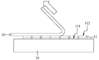
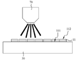
상기 복수 개의 다이의 제1 표면 상의 미세 입자를 클리어링하는 단계;
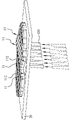
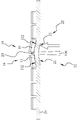
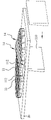
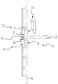
상기 복수 개의 다이의 제2 표면의 복수 개의 측변 및 복수 개의 코너를 상기 복수 개의 타깃 블록으로부터 박리하는 단계;
상기 캐리어 필름을 뒤집고, 상기 복수 개의 다이를 제1 캐리어로 이송하되, 상기 복수 개의 다이의 제1 표면은 제1 캐리어와 접촉하는 단계;
상기 캐리어 필름을 상기 복수 개의 다이의 제2 표면으로부터 제거하는 단계;
상기 복수 개의 다이의 제2 표면 상의 미세 입자를 클리어링하는 단계; 및
상기 복수 개의 다이를 상기 제1 캐리어에서 기판으로 이송하되, 상기 기판의 표면에는 솔더와 범프가 없는 단계를 포함하는 것을 특징으로 하는 다이 고정을 위한 하이브리드 본딩 방법. - 제1항에 있어서,
상기 복수 개의 다이의 제1 표면 상의 미세 입자를 클리어링하는 단계 후, 상기 캐리어 필름을 디본딩하는 단계를 더 포함하는 것을 특징으로 하는 다이 고정을 위한 하이브리드 본딩 방법. - 제2항에 있어서,
상기 캐리어 필름을 디본딩하는 단계는, 상기 캐리어 필름을 UV 이형 필름으로 하고, 자외선을 상기 캐리어 필름에 조사하는 단계인 것을 특징으로 하는 다이 고정을 위한 하이브리드 본딩 방법. - 제2항에 있어서,
상기 캐리어 필름을 디본딩하는 단계는, 상기 캐리어 필름을 열 이형 필름으로 하고, 상기 캐리어 필름을 가열하는 단계인 것을 특징으로 하는 다이 고정을 위한 하이브리드 본딩 방법. - 제1항에 있어서,
상기 웨이퍼가 상기 복수 개의 다이로 절단되는 단계는, 상기 웨이퍼가 여러 열의 다이 조합으로 절단되는 단계를 더 포함하고, 각 열의 다이 조합은 여러 개의 다이를 포함하며, 여러 열의 다이 조합은 상기 캐리어 필름의 여러 열의 타깃 블록 조합에 분포되고, 각 열의 타깃 블록 조합은 여러 개의 타깃 블록을 포함하며; 상기 복수 개의 다이의 제2 표면의 상기 복수 개의 측변 및 상기 복수 개의 코너를 상기 복수 개의 타깃 블록으로부터 박리하는 단계는, 인접한 두 열의 타깃 블록 조합의 2개의 타깃 블록이 위로 돌출되거나 아래로 함몰되어, 인접한 두 열의 다이 조합의 모든 다이의 제2 표면의 상기 복수 개의 측변 및 상기 복수 개의 코너가 인접한 두 열의 타깃 블록 조합의 모든 타깃 블록으로부터 박리되는 단계; 및 그 중 두 열의 다이 조합에 대한 박리 절차가 완료된 후, 여러 열의 다이 조합에 대한 박리 절차가 모두 완료될 때까지 다른 두 열의 다이 조합에 대한 박리 절차를 계속 수행하는 단계를 더 포함하는 것을 특징으로 하는 다이 고정을 위한 하이브리드 본딩 방법. - 제1항에 있어서,
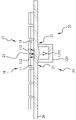
상기 복수 개의 다이의 제2 표면의 상기 복수 개의 측변 및 상기 복수 개의 코너를 상기 복수 개의 타깃 블록으로부터 박리하는 단계는, 적어도 하나의 푸시 부재가 위로 이동하여 상기 복수 개의 타깃 블록 사이의 연결 블록을 순차적으로 푸시함으로써, 상기 복수 개의 타깃 블록이 위로 돌출되어, 상기 복수 개의 다이의 제2 표면의 상기 복수 개의 측변 및 상기 복수 개의 코너가 상기 복수 개의 타깃 블록으로부터 박리되는 단계를 더 포함하는 것을 특징으로 하는 다이 고정을 위한 하이브리드 본딩 방법. - 제1항에 있어서,
상기 복수 개의 다이의 제2 표면의 상기 복수 개의 측변 및 상기 복수 개의 코너를 상기 복수 개의 타깃 블록으로부터 박리하는 단계는, 스크레이퍼가 상기 캐리어 필름의 표면을 따라 수평 이동하여 상기 복수 개의 타깃 블록 사이의 연결 블록을 순차적으로 푸시함으로써, 상기 복수 개의 타깃 블록이 위로 돌출되어, 상기 복수 개의 다이의 제2 표면의 상기 복수 개의 측변 및 상기 복수 개의 코너가 상기 복수 개의 타깃 블록으로부터 박리되는 단계를 더 포함하는 것을 특징으로 하는 다이 고정을 위한 하이브리드 본딩 방법. - 제1항에 있어서,
상기 복수 개의 다이의 제2 표면의 상기 복수 개의 측변 및 상기 복수 개의 코너를 상기 복수 개의 타깃 블록으로부터 박리하는 단계는, 흡착 장치의 적어도 하나의 채널이 부압을 제공하고, 상기 복수 개의 타깃 블록 사이의 연결 블록을 순차적으로 흡착함으로써, 상기 복수 개의 타깃 블록이 아래로 함몰되어, 상기 복수 개의 다이의 제2 표면의 상기 복수 개의 측변 및 상기 복수 개의 코너가 상기 복수 개의 타깃 블록으로부터 박리되는 단계를 더 포함하는 것을 특징으로 하는 다이 고정을 위한 하이브리드 본딩 방법. - 제1항에 있어서,
상기 복수 개의 다이를 상기 제1 캐리어에서 상기 기판으로 이송하는 단계는, 상기 제1 캐리어로부터 상기 복수 개의 다이를 픽업하는 단계; 상기 복수 개의 다이를 이동하는 단계; 및 상기 복수 개의 다이를 상기 기판에 안착하되, 상기 복수 개의 다이의 제1 표면은 상기 기판과 접촉하는 단계를 더 포함하는 것을 특징으로 하는 다이 고정을 위한 하이브리드 본딩 방법. - 제1항에 있어서,
상기 복수 개의 다이를 상기 제1 캐리어에서 상기 기판으로 이송하는 단계는, 상기 제1 캐리어를 뒤집고, 상기 복수 개의 다이를 제2 캐리어로 이송하되, 상기 복수 개의 다이의 제2 표면은 상기 제2 캐리어와 접촉하는 단계; 상기 복수 개의 다이의 제1 표면 상의 미세 입자를 클리어링하는 단계; 상기 제2 캐리어로부터 상기 복수 개의 다이를 픽업하는 단계; 상기 복수 개의 다이를 이동하는 단계; 및 상기 복수 개의 다이를 상기 기판에 안착하되, 상기 복수 개의 다이의 제2 표면은 상기 기판과 접촉하는 단계를 더 포함하는 것을 특징으로 하는 다이 고정을 위한 하이브리드 본딩 방법.
Applications Claiming Priority (2)
| Application Number | Priority Date | Filing Date | Title |
|---|---|---|---|
| US202163189468P | 2021-05-17 | 2021-05-17 | |
| US63/189,468 | 2021-05-17 |
Publications (2)
| Publication Number | Publication Date |
|---|---|
| KR20220155893A true KR20220155893A (ko) | 2022-11-24 |
| KR102772060B1 KR102772060B1 (ko) | 2025-02-25 |
Family
ID=83998009
Family Applications (1)
| Application Number | Title | Priority Date | Filing Date |
|---|---|---|---|
| KR1020220009754A Active KR102772060B1 (ko) | 2021-05-17 | 2022-01-24 | 다이 고정을 위한 하이브리드 본딩 방법 |
Country Status (4)
| Country | Link |
|---|---|
| US (1) | US12322639B2 (ko) |
| KR (1) | KR102772060B1 (ko) |
| CN (1) | CN115360100A (ko) |
| TW (1) | TWI868417B (ko) |
Families Citing this family (3)
| Publication number | Priority date | Publication date | Assignee | Title |
|---|---|---|---|---|
| US20240170443A1 (en) * | 2022-11-18 | 2024-05-23 | Applied Materials, Inc. | Integrated process flows for hybrid bonding |
| TWI834450B (zh) * | 2022-12-26 | 2024-03-01 | 梭特科技股份有限公司 | 利用頂出手段結合氣壓控制手段的晶粒剝離方法 |
| TWI846653B (zh) * | 2023-12-07 | 2024-06-21 | 梭特科技股份有限公司 | 槽狀晶粒剝離裝置及方法 |
Citations (7)
| Publication number | Priority date | Publication date | Assignee | Title |
|---|---|---|---|---|
| JP2005340431A (ja) * | 2004-05-26 | 2005-12-08 | Renesas Technology Corp | 半導体装置の製造方法 |
| JP2006324703A (ja) * | 2006-09-06 | 2006-11-30 | Renesas Technology Corp | 半導体装置の製造方法 |
| KR20080074867A (ko) * | 2008-04-30 | 2008-08-13 | 가부시끼가이샤 르네사스 테크놀로지 | 반도체 장치의 제조 방법 |
| KR20110084269A (ko) * | 2008-10-28 | 2011-07-21 | 파나소닉 전공 주식회사 | 반도체 발광 소자의 제조 방법 |
| JP2019067819A (ja) * | 2017-09-28 | 2019-04-25 | パナソニックIpマネジメント株式会社 | 素子チップの製造方法及び装置 |
| KR20190133256A (ko) * | 2017-04-21 | 2019-12-02 | 인벤사스 본딩 테크놀로지스 인코포레이티드 | 다이 처리 |
| JP2020509578A (ja) * | 2017-03-02 | 2020-03-26 | エーファウ・グループ・エー・タルナー・ゲーエムベーハー | チップを接合する方法および装置 |
Family Cites Families (4)
| Publication number | Priority date | Publication date | Assignee | Title |
|---|---|---|---|---|
| US9034733B2 (en) * | 2012-08-20 | 2015-05-19 | Semiconductor Components Industries, Llc | Semiconductor die singulation method |
| US9484260B2 (en) * | 2012-11-07 | 2016-11-01 | Semiconductor Components Industries, Llc | Heated carrier substrate semiconductor die singulation method |
| KR102700207B1 (ko) * | 2019-03-12 | 2024-08-28 | 삼성전자주식회사 | 칩 이젝팅 장치 |
| TWM587817U (zh) * | 2019-05-17 | 2019-12-11 | 瑋鋒科技股份有限公司 | 晶圓接合膜 |
-
2022
- 2022-01-05 TW TW111100430A patent/TWI868417B/zh active
- 2022-01-21 CN CN202210071306.0A patent/CN115360100A/zh active Pending
- 2022-01-24 KR KR1020220009754A patent/KR102772060B1/ko active Active
- 2022-03-04 US US17/686,661 patent/US12322639B2/en active Active
Patent Citations (7)
| Publication number | Priority date | Publication date | Assignee | Title |
|---|---|---|---|---|
| JP2005340431A (ja) * | 2004-05-26 | 2005-12-08 | Renesas Technology Corp | 半導体装置の製造方法 |
| JP2006324703A (ja) * | 2006-09-06 | 2006-11-30 | Renesas Technology Corp | 半導体装置の製造方法 |
| KR20080074867A (ko) * | 2008-04-30 | 2008-08-13 | 가부시끼가이샤 르네사스 테크놀로지 | 반도체 장치의 제조 방법 |
| KR20110084269A (ko) * | 2008-10-28 | 2011-07-21 | 파나소닉 전공 주식회사 | 반도체 발광 소자의 제조 방법 |
| JP2020509578A (ja) * | 2017-03-02 | 2020-03-26 | エーファウ・グループ・エー・タルナー・ゲーエムベーハー | チップを接合する方法および装置 |
| KR20190133256A (ko) * | 2017-04-21 | 2019-12-02 | 인벤사스 본딩 테크놀로지스 인코포레이티드 | 다이 처리 |
| JP2019067819A (ja) * | 2017-09-28 | 2019-04-25 | パナソニックIpマネジメント株式会社 | 素子チップの製造方法及び装置 |
Also Published As
| Publication number | Publication date |
|---|---|
| TWI868417B (zh) | 2025-01-01 |
| KR102772060B1 (ko) | 2025-02-25 |
| CN115360100A (zh) | 2022-11-18 |
| TW202247300A (zh) | 2022-12-01 |
| US20220367232A1 (en) | 2022-11-17 |
| US12322639B2 (en) | 2025-06-03 |
Similar Documents
| Publication | Publication Date | Title |
|---|---|---|
| KR20220155893A (ko) | 다이 고정을 위한 하이브리드 본딩 방법 | |
| TWI847991B (zh) | 用於混合接合的後化學機械研磨處理 | |
| KR102320674B1 (ko) | 처리된 적층 다이들 | |
| US9472518B2 (en) | Semiconductor structures including carrier wafers and methods of using such semiconductor structures | |
| KR101579772B1 (ko) | 웨이퍼 레벨 싱귤레이션 방법 및 시스템 | |
| JP6189700B2 (ja) | ウエーハの加工方法 | |
| TWI745532B (zh) | 半導體基板之處理方法及處理裝置 | |
| JPH0574224B2 (ko) | ||
| KR102821752B1 (ko) | 분리 장치 및 분리 방법 | |
| US10804131B2 (en) | Carrier plate removing method | |
| KR101006526B1 (ko) | 웨이퍼 마운트 테이프, 이를 이용한 웨이퍼 가공 장치 및 방법 | |
| US11764066B2 (en) | Peeling method for peeling off substrate from support plate | |
| US20230377938A1 (en) | Chip bonding method | |
| US20060003491A1 (en) | Apparatus for ejecting relatively thin IC chip from semiconductor wafer | |
| US11538710B2 (en) | Carrier plate removing method | |
| KR100539271B1 (ko) | 휨 방지 재질을 사용하는 반도체 칩의 다이 접착 방법 | |
| JP2004311980A (ja) | 半導体製造装置及び半導体装置の製造方法 | |
| US20100051190A1 (en) | Method for applying an adhesive layer on thin cut semiconductor chips of semiconductor wafers | |
| JP6616457B2 (ja) | チップの接合方法及びチップの接合装置 | |
| JP7262891B2 (ja) | ダミーウェーハ及びダミーウェーハの製造方法 | |
| JP7451028B2 (ja) | 保護シートの配設方法 | |
| CN112038220B (zh) | 晶圆键合工艺中改善晶圆边缘形变的方法 | |
| JP2025064379A (ja) | 板状物の加工方法 | |
| TW202329225A (zh) | 晶圓切割方法 | |
| CN101621025B (zh) | 分离晶片基材上表层的多个半导体元件裸片方法 |
Legal Events
| Date | Code | Title | Description |
|---|---|---|---|
| PA0109 | Patent application |
Patent event code: PA01091R01D Comment text: Patent Application Patent event date: 20220124 |
|
| PA0201 | Request for examination | ||
| PG1501 | Laying open of application | ||
| E902 | Notification of reason for refusal | ||
| PE0902 | Notice of grounds for rejection |
Comment text: Notification of reason for refusal Patent event date: 20240124 Patent event code: PE09021S01D |
|
| PE0902 | Notice of grounds for rejection |
Comment text: Final Notice of Reason for Refusal Patent event date: 20240924 Patent event code: PE09021S02D |
|
| E701 | Decision to grant or registration of patent right | ||
| PE0701 | Decision of registration |
Patent event code: PE07011S01D Comment text: Decision to Grant Registration Patent event date: 20250124 |
|
| GRNT | Written decision to grant | ||
| PR0701 | Registration of establishment |
Comment text: Registration of Establishment Patent event date: 20250219 Patent event code: PR07011E01D |
|
| PR1002 | Payment of registration fee |
Payment date: 20250220 End annual number: 3 Start annual number: 1 |
|
| PG1601 | Publication of registration |