KR20210134503A - Substrate processing apparatus, stage, and temperature control method - Google Patents
Substrate processing apparatus, stage, and temperature control method Download PDFInfo
- Publication number
- KR20210134503A KR20210134503A KR1020210051048A KR20210051048A KR20210134503A KR 20210134503 A KR20210134503 A KR 20210134503A KR 1020210051048 A KR1020210051048 A KR 1020210051048A KR 20210051048 A KR20210051048 A KR 20210051048A KR 20210134503 A KR20210134503 A KR 20210134503A
- Authority
- KR
- South Korea
- Prior art keywords
- plate
- temperature
- temperature control
- control mechanism
- shape
- Prior art date
Links
- 239000000758 substrate Substances 0.000 title claims abstract description 112
- 238000000034 method Methods 0.000 title claims description 35
- 230000001276 controlling effect Effects 0.000 claims description 22
- 229910052751 metal Inorganic materials 0.000 claims description 3
- 239000002184 metal Substances 0.000 claims description 3
- 230000000149 penetrating effect Effects 0.000 claims description 3
- 230000001105 regulatory effect Effects 0.000 claims description 3
- 230000035882 stress Effects 0.000 description 20
- 230000008646 thermal stress Effects 0.000 description 15
- 230000009466 transformation Effects 0.000 description 10
- 230000008602 contraction Effects 0.000 description 7
- 238000010586 diagram Methods 0.000 description 7
- 229910052782 aluminium Inorganic materials 0.000 description 6
- XAGFODPZIPBFFR-UHFFFAOYSA-N aluminium Chemical compound [Al] XAGFODPZIPBFFR-UHFFFAOYSA-N 0.000 description 6
- 230000007797 corrosion Effects 0.000 description 6
- 238000005260 corrosion Methods 0.000 description 6
- 238000005259 measurement Methods 0.000 description 6
- 238000005530 etching Methods 0.000 description 5
- 239000004020 conductor Substances 0.000 description 4
- PNEYBMLMFCGWSK-UHFFFAOYSA-N aluminium oxide Inorganic materials [O-2].[O-2].[O-2].[Al+3].[Al+3] PNEYBMLMFCGWSK-UHFFFAOYSA-N 0.000 description 3
- 238000005452 bending Methods 0.000 description 3
- 239000000919 ceramic Substances 0.000 description 3
- 238000009792 diffusion process Methods 0.000 description 3
- 150000002500 ions Chemical class 0.000 description 3
- SIWVEOZUMHYXCS-UHFFFAOYSA-N oxo(oxoyttriooxy)yttrium Chemical compound O=[Y]O[Y]=O SIWVEOZUMHYXCS-UHFFFAOYSA-N 0.000 description 3
- RTAQQCXQSZGOHL-UHFFFAOYSA-N Titanium Chemical compound [Ti] RTAQQCXQSZGOHL-UHFFFAOYSA-N 0.000 description 2
- 239000012790 adhesive layer Substances 0.000 description 2
- 238000000231 atomic layer deposition Methods 0.000 description 2
- 230000008094 contradictory effect Effects 0.000 description 2
- 239000011810 insulating material Substances 0.000 description 2
- 230000002093 peripheral effect Effects 0.000 description 2
- 239000003507 refrigerant Substances 0.000 description 2
- 239000010936 titanium Substances 0.000 description 2
- 229910052719 titanium Inorganic materials 0.000 description 2
- BSYNRYMUTXBXSQ-UHFFFAOYSA-N Aspirin Chemical compound CC(=O)OC1=CC=CC=C1C(O)=O BSYNRYMUTXBXSQ-UHFFFAOYSA-N 0.000 description 1
- 238000002048 anodisation reaction Methods 0.000 description 1
- 238000004380 ashing Methods 0.000 description 1
- 239000006227 byproduct Substances 0.000 description 1
- 239000007795 chemical reaction product Substances 0.000 description 1
- 238000009616 inductively coupled plasma Methods 0.000 description 1
- 239000012528 membrane Substances 0.000 description 1
- 238000002488 metal-organic chemical vapour deposition Methods 0.000 description 1
- TWNQGVIAIRXVLR-UHFFFAOYSA-N oxo(oxoalumanyloxy)alumane Chemical compound O=[Al]O[Al]=O TWNQGVIAIRXVLR-UHFFFAOYSA-N 0.000 description 1
- 238000003672 processing method Methods 0.000 description 1
- 239000004065 semiconductor Substances 0.000 description 1
- 229910052710 silicon Inorganic materials 0.000 description 1
- 239000010703 silicon Substances 0.000 description 1
- 238000004544 sputter deposition Methods 0.000 description 1
Images


Classifications
-
- H—ELECTRICITY
- H01—ELECTRIC ELEMENTS
- H01L—SEMICONDUCTOR DEVICES NOT COVERED BY CLASS H10
- H01L21/00—Processes or apparatus adapted for the manufacture or treatment of semiconductor or solid state devices or of parts thereof
- H01L21/67—Apparatus specially adapted for handling semiconductor or electric solid state devices during manufacture or treatment thereof; Apparatus specially adapted for handling wafers during manufacture or treatment of semiconductor or electric solid state devices or components ; Apparatus not specifically provided for elsewhere
- H01L21/683—Apparatus specially adapted for handling semiconductor or electric solid state devices during manufacture or treatment thereof; Apparatus specially adapted for handling wafers during manufacture or treatment of semiconductor or electric solid state devices or components ; Apparatus not specifically provided for elsewhere for supporting or gripping
- H01L21/6831—Apparatus specially adapted for handling semiconductor or electric solid state devices during manufacture or treatment thereof; Apparatus specially adapted for handling wafers during manufacture or treatment of semiconductor or electric solid state devices or components ; Apparatus not specifically provided for elsewhere for supporting or gripping using electrostatic chucks
- H01L21/6833—Details of electrostatic chucks
-
- H—ELECTRICITY
- H01—ELECTRIC ELEMENTS
- H01J—ELECTRIC DISCHARGE TUBES OR DISCHARGE LAMPS
- H01J37/00—Discharge tubes with provision for introducing objects or material to be exposed to the discharge, e.g. for the purpose of examination or processing thereof
- H01J37/32—Gas-filled discharge tubes
- H01J37/32431—Constructional details of the reactor
- H01J37/32715—Workpiece holder
- H01J37/32724—Temperature
-
- B—PERFORMING OPERATIONS; TRANSPORTING
- B23—MACHINE TOOLS; METAL-WORKING NOT OTHERWISE PROVIDED FOR
- B23Q—DETAILS, COMPONENTS, OR ACCESSORIES FOR MACHINE TOOLS, e.g. ARRANGEMENTS FOR COPYING OR CONTROLLING; MACHINE TOOLS IN GENERAL CHARACTERISED BY THE CONSTRUCTION OF PARTICULAR DETAILS OR COMPONENTS; COMBINATIONS OR ASSOCIATIONS OF METAL-WORKING MACHINES, NOT DIRECTED TO A PARTICULAR RESULT
- B23Q3/00—Devices holding, supporting, or positioning work or tools, of a kind normally removable from the machine
- B23Q3/15—Devices for holding work using magnetic or electric force acting directly on the work
-
- C—CHEMISTRY; METALLURGY
- C23—COATING METALLIC MATERIAL; COATING MATERIAL WITH METALLIC MATERIAL; CHEMICAL SURFACE TREATMENT; DIFFUSION TREATMENT OF METALLIC MATERIAL; COATING BY VACUUM EVAPORATION, BY SPUTTERING, BY ION IMPLANTATION OR BY CHEMICAL VAPOUR DEPOSITION, IN GENERAL; INHIBITING CORROSION OF METALLIC MATERIAL OR INCRUSTATION IN GENERAL
- C23C—COATING METALLIC MATERIAL; COATING MATERIAL WITH METALLIC MATERIAL; SURFACE TREATMENT OF METALLIC MATERIAL BY DIFFUSION INTO THE SURFACE, BY CHEMICAL CONVERSION OR SUBSTITUTION; COATING BY VACUUM EVAPORATION, BY SPUTTERING, BY ION IMPLANTATION OR BY CHEMICAL VAPOUR DEPOSITION, IN GENERAL
- C23C16/00—Chemical coating by decomposition of gaseous compounds, without leaving reaction products of surface material in the coating, i.e. chemical vapour deposition [CVD] processes
- C23C16/44—Chemical coating by decomposition of gaseous compounds, without leaving reaction products of surface material in the coating, i.e. chemical vapour deposition [CVD] processes characterised by the method of coating
- C23C16/458—Chemical coating by decomposition of gaseous compounds, without leaving reaction products of surface material in the coating, i.e. chemical vapour deposition [CVD] processes characterised by the method of coating characterised by the method used for supporting substrates in the reaction chamber
- C23C16/4582—Rigid and flat substrates, e.g. plates or discs
- C23C16/4583—Rigid and flat substrates, e.g. plates or discs the substrate being supported substantially horizontally
- C23C16/4586—Elements in the interior of the support, e.g. electrodes, heating or cooling devices
-
- F—MECHANICAL ENGINEERING; LIGHTING; HEATING; WEAPONS; BLASTING
- F28—HEAT EXCHANGE IN GENERAL
- F28F—DETAILS OF HEAT-EXCHANGE AND HEAT-TRANSFER APPARATUS, OF GENERAL APPLICATION
- F28F27/00—Control arrangements or safety devices specially adapted for heat-exchange or heat-transfer apparatus
-
- H—ELECTRICITY
- H01—ELECTRIC ELEMENTS
- H01L—SEMICONDUCTOR DEVICES NOT COVERED BY CLASS H10
- H01L21/00—Processes or apparatus adapted for the manufacture or treatment of semiconductor or solid state devices or of parts thereof
- H01L21/67—Apparatus specially adapted for handling semiconductor or electric solid state devices during manufacture or treatment thereof; Apparatus specially adapted for handling wafers during manufacture or treatment of semiconductor or electric solid state devices or components ; Apparatus not specifically provided for elsewhere
- H01L21/67005—Apparatus not specifically provided for elsewhere
- H01L21/67011—Apparatus for manufacture or treatment
- H01L21/67098—Apparatus for thermal treatment
- H01L21/67109—Apparatus for thermal treatment mainly by convection
-
- H—ELECTRICITY
- H01—ELECTRIC ELEMENTS
- H01L—SEMICONDUCTOR DEVICES NOT COVERED BY CLASS H10
- H01L21/00—Processes or apparatus adapted for the manufacture or treatment of semiconductor or solid state devices or of parts thereof
- H01L21/67—Apparatus specially adapted for handling semiconductor or electric solid state devices during manufacture or treatment thereof; Apparatus specially adapted for handling wafers during manufacture or treatment of semiconductor or electric solid state devices or components ; Apparatus not specifically provided for elsewhere
- H01L21/67005—Apparatus not specifically provided for elsewhere
- H01L21/67242—Apparatus for monitoring, sorting or marking
- H01L21/67248—Temperature monitoring
-
- H—ELECTRICITY
- H01—ELECTRIC ELEMENTS
- H01L—SEMICONDUCTOR DEVICES NOT COVERED BY CLASS H10
- H01L21/00—Processes or apparatus adapted for the manufacture or treatment of semiconductor or solid state devices or of parts thereof
- H01L21/67—Apparatus specially adapted for handling semiconductor or electric solid state devices during manufacture or treatment thereof; Apparatus specially adapted for handling wafers during manufacture or treatment of semiconductor or electric solid state devices or components ; Apparatus not specifically provided for elsewhere
- H01L21/67005—Apparatus not specifically provided for elsewhere
- H01L21/67242—Apparatus for monitoring, sorting or marking
- H01L21/67288—Monitoring of warpage, curvature, damage, defects or the like
-
- H—ELECTRICITY
- H01—ELECTRIC ELEMENTS
- H01L—SEMICONDUCTOR DEVICES NOT COVERED BY CLASS H10
- H01L21/00—Processes or apparatus adapted for the manufacture or treatment of semiconductor or solid state devices or of parts thereof
- H01L21/67—Apparatus specially adapted for handling semiconductor or electric solid state devices during manufacture or treatment thereof; Apparatus specially adapted for handling wafers during manufacture or treatment of semiconductor or electric solid state devices or components ; Apparatus not specifically provided for elsewhere
- H01L21/683—Apparatus specially adapted for handling semiconductor or electric solid state devices during manufacture or treatment thereof; Apparatus specially adapted for handling wafers during manufacture or treatment of semiconductor or electric solid state devices or components ; Apparatus not specifically provided for elsewhere for supporting or gripping
- H01L21/6831—Apparatus specially adapted for handling semiconductor or electric solid state devices during manufacture or treatment thereof; Apparatus specially adapted for handling wafers during manufacture or treatment of semiconductor or electric solid state devices or components ; Apparatus not specifically provided for elsewhere for supporting or gripping using electrostatic chucks
-
- H—ELECTRICITY
- H01—ELECTRIC ELEMENTS
- H01L—SEMICONDUCTOR DEVICES NOT COVERED BY CLASS H10
- H01L21/00—Processes or apparatus adapted for the manufacture or treatment of semiconductor or solid state devices or of parts thereof
- H01L21/67—Apparatus specially adapted for handling semiconductor or electric solid state devices during manufacture or treatment thereof; Apparatus specially adapted for handling wafers during manufacture or treatment of semiconductor or electric solid state devices or components ; Apparatus not specifically provided for elsewhere
- H01L21/683—Apparatus specially adapted for handling semiconductor or electric solid state devices during manufacture or treatment thereof; Apparatus specially adapted for handling wafers during manufacture or treatment of semiconductor or electric solid state devices or components ; Apparatus not specifically provided for elsewhere for supporting or gripping
- H01L21/687—Apparatus specially adapted for handling semiconductor or electric solid state devices during manufacture or treatment thereof; Apparatus specially adapted for handling wafers during manufacture or treatment of semiconductor or electric solid state devices or components ; Apparatus not specifically provided for elsewhere for supporting or gripping using mechanical means, e.g. chucks, clamps or pinches
- H01L21/68714—Apparatus specially adapted for handling semiconductor or electric solid state devices during manufacture or treatment thereof; Apparatus specially adapted for handling wafers during manufacture or treatment of semiconductor or electric solid state devices or components ; Apparatus not specifically provided for elsewhere for supporting or gripping using mechanical means, e.g. chucks, clamps or pinches the wafers being placed on a susceptor, stage or support
- H01L21/68785—Apparatus specially adapted for handling semiconductor or electric solid state devices during manufacture or treatment thereof; Apparatus specially adapted for handling wafers during manufacture or treatment of semiconductor or electric solid state devices or components ; Apparatus not specifically provided for elsewhere for supporting or gripping using mechanical means, e.g. chucks, clamps or pinches the wafers being placed on a susceptor, stage or support characterised by the mechanical construction of the susceptor, stage or support
-
- H—ELECTRICITY
- H02—GENERATION; CONVERSION OR DISTRIBUTION OF ELECTRIC POWER
- H02N—ELECTRIC MACHINES NOT OTHERWISE PROVIDED FOR
- H02N13/00—Clutches or holding devices using electrostatic attraction, e.g. using Johnson-Rahbek effect
-
- C—CHEMISTRY; METALLURGY
- C23—COATING METALLIC MATERIAL; COATING MATERIAL WITH METALLIC MATERIAL; CHEMICAL SURFACE TREATMENT; DIFFUSION TREATMENT OF METALLIC MATERIAL; COATING BY VACUUM EVAPORATION, BY SPUTTERING, BY ION IMPLANTATION OR BY CHEMICAL VAPOUR DEPOSITION, IN GENERAL; INHIBITING CORROSION OF METALLIC MATERIAL OR INCRUSTATION IN GENERAL
- C23C—COATING METALLIC MATERIAL; COATING MATERIAL WITH METALLIC MATERIAL; SURFACE TREATMENT OF METALLIC MATERIAL BY DIFFUSION INTO THE SURFACE, BY CHEMICAL CONVERSION OR SUBSTITUTION; COATING BY VACUUM EVAPORATION, BY SPUTTERING, BY ION IMPLANTATION OR BY CHEMICAL VAPOUR DEPOSITION, IN GENERAL
- C23C16/00—Chemical coating by decomposition of gaseous compounds, without leaving reaction products of surface material in the coating, i.e. chemical vapour deposition [CVD] processes
- C23C16/44—Chemical coating by decomposition of gaseous compounds, without leaving reaction products of surface material in the coating, i.e. chemical vapour deposition [CVD] processes characterised by the method of coating
- C23C16/46—Chemical coating by decomposition of gaseous compounds, without leaving reaction products of surface material in the coating, i.e. chemical vapour deposition [CVD] processes characterised by the method of coating characterised by the method used for heating the substrate
Abstract
Description
본 개시는, 기판 처리 장치, 적재대 및 온도 제어 방법에 관한 것이다.The present disclosure relates to a substrate processing apparatus, a mounting table, and a temperature control method.
프로세스에 의해 기판에 휨 등의 변형이 생기는 경우가 알려져 있다(예를 들어, 특허문헌 1 참조). 또한, 열응력에 의해 적재대에 휨 등의 변형이 생기는 경우가 알려져 있다(예를 들어, 특허문헌 2 참조).It is known that the substrate undergoes deformation such as warpage due to the process (for example, refer to Patent Document 1). Moreover, it is known that a deformation|transformation, such as curvature, arises in a mounting table by thermal stress (for example, refer patent document 2).
본 개시는, 적재대의 변형을 제어할 수 있는 기술을 제공한다.The present disclosure provides a technique capable of controlling the deformation of the mounting table.
본 개시의 일 양태에 의하면, 기판을 적재하는 적재대를 갖는 기판 처리 장치이며, 상기 적재대는, 제1 플레이트와, 상기 제1 플레이트의 온도를 제어하는 제1 온도 조절 기구와, 상기 제1 플레이트의 하부에 배치되는 제2 플레이트와, 상기 제2 플레이트의 온도를 제어하는 제2 온도 조절 기구와, 상기 제1 플레이트와 상기 제2 플레이트를 체결하는 체결 부재를 갖는 기판 처리 장치가 제공된다.According to one aspect of the present disclosure, there is provided a substrate processing apparatus having a mounting table for mounting a substrate, the mounting table including a first plate, a first temperature control mechanism for controlling a temperature of the first plate, and the first plate There is provided a substrate processing apparatus having a second plate disposed under
일 측면에 의하면, 적재대의 변형을 제어할 수 있다.According to one aspect, it is possible to control the deformation of the mounting table.
도 1은 실시 형태에 따른 기판 처리 장치의 일례를 도시하는 단면 모식도이다.
도 2는 실시 형태에 따른 적재대의 온도 제어의 일례를 도시하는 도면이다.
도 3은 실시 형태에 따른 적재대의 온도 제어의 일례를 도시하는 도면이다.
도 4는 실시 형태에 따른 적재대의 온도 제어의 다른 예를 도시하는 도면이다.
도 5는 실시 형태에 따른 적재대의 온도 제어의 다른 예를 도시하는 도면이다.
도 6은 실시 형태에 따른 온도 제어 방법의 일례를 도시하는 도면이다.
도 7은 실시 형태에 따른 복수의 센서의 배치 예를 도시하는 도면이다.BRIEF DESCRIPTION OF THE DRAWINGS It is a cross-sectional schematic diagram which shows an example of the substrate processing apparatus which concerns on embodiment.
It is a figure which shows an example of the temperature control of the mounting table which concerns on embodiment.
It is a figure which shows an example of the temperature control of the mounting table which concerns on embodiment.
It is a figure which shows the other example of the temperature control of the mounting table which concerns on embodiment.
It is a figure which shows the other example of the temperature control of the mounting table which concerns on embodiment.
It is a figure which shows an example of the temperature control method which concerns on embodiment.
7 is a diagram illustrating an arrangement example of a plurality of sensors according to the embodiment.
이하, 도면을 참조하여 본 개시를 실시하기 위한 형태에 대해서 설명한다. 각 도면에 있어서, 동일 구성 부분에는 동일 부호를 붙이고, 중복된 설명을 생략하는 경우가 있다.EMBODIMENT OF THE INVENTION Hereinafter, the form for implementing this indication with reference to drawings is demonstrated. In each figure, the same code|symbol is attached|subjected to the same structural part, and overlapping description may be abbreviate|omitted.
[기판 처리 장치][Substrate processing unit]
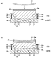
먼저, 실시 형태에 따른 기판 처리 장치의 일례에 대해서, 도 1을 참조하면서 설명한다. 도 1은, 실시 형태에 따른 기판 처리 장치의 일례를 도시하는 도면이다. 기판 처리 장치(1)는 용량 결합형 장치이다.First, an example of the substrate processing apparatus which concerns on embodiment is demonstrated, referring FIG. 1 is a diagram illustrating an example of a substrate processing apparatus according to an embodiment. The
기판 처리 장치(1)는 챔버(10)를 갖는다. 챔버(10)는, 그 안에 내부 공간(10s)을 제공하고 있다. 챔버(10)는 챔버 본체(12)를 포함하고 있다. 챔버 본체(12)는, 대략 원통 형상을 갖고 있다. 내부 공간(10s)은 챔버 본체(12)의 내측에 제공되어 있다. 챔버 본체(12)는 예를 들어 알루미늄으로 형성되어 있다. 챔버 본체(12)의 내벽면 상에는, 내식성을 갖는 막이 마련되어 있다. 내식성을 갖는 막은, 알루미나(산화알루미늄), 산화이트륨과 같은 세라믹스로 형성되고, 양극 산화 처리된 산화막일 수 있다.The
챔버 본체(12)의 측벽에는 통로(12p)가 형성되어 있다. 기판(W)은, 내부 공간(10s)과 챔버(10)의 외부 사이에서 반송될 때, 통로(12p)를 통과한다. 통로(12p)는 게이트 밸브(12g)에 의해 개폐 가능하게 되어 있다. 게이트 밸브(12g)는 챔버 본체(12)의 측벽을 따라 마련되어 있다.A
챔버 본체(12)의 저부 상에는, 지지부(13)가 마련되어 있다. 지지부(13)는 절연 재료로 형성되어 있다. 지지부(13)는, 대략 원통 형상을 갖고 있다. 지지부(13)는, 내부 공간(10s) 내에서, 챔버 본체(12)의 저부로부터 상방으로 연장되어 있다. 지지부(13) 상에는, 기판의 주위를 둘러싸는 에지 링(25)(포커스 링이라고도 불림)이 마련되어 있다. 에지 링(25)은, 대략 원통 형상을 갖고, 실리콘 등으로 형성되어도 된다.On the bottom of the
기판 처리 장치(1)는 적재대(14)를 더 구비하고 있다. 적재대(14)는 지지부(13)에 의해 지지되어 있다. 적재대(14)는 내부 공간(10s) 내에 마련되어 있다. 적재대(14)는 챔버(10) 내, 즉 내부 공간(10s) 내에서 기판(W)을 지지하도록 구성되어 있다.The
적재대(14)는, 제1 플레이트(18) 및 하나의 예시적 실시 형태에 따른 정전 척(20)을 갖고 있다. 적재대(14)는 제2 플레이트(16)를 더 가질 수 있다. 제2 플레이트(16)는, 예를 들어 알루미늄 또는 티타늄과 같은 도체로 형성되어 있고, 대략 원반 형상을 갖고 있다. 제1 플레이트(18)는 제2 플레이트(16)의 상부에 마련되어 있다. 제1 플레이트(18)는, 예를 들어 알루미늄 또는 티타늄과 같은 도체로 형성되어 있고, 대략 원반 형상을 갖고 있다. 제1 플레이트(18) 및 제2 플레이트(16)는 세라믹스에 의해 구성해도 된다. 단, 제1 플레이트(18) 및 제2 플레이트(16)는, 동종의 금속(도전성 부재)으로 구성되는 것이 바람직하다. 제1 플레이트(18) 및 제2 플레이트(16)를 도전성 부재에 의해 구성함으로써, 세라믹스에 의해 구성하는 것보다도 제1 플레이트(18)와 제2 플레이트(16)의 마찰이 커진다. 이 때문에, 후술하는 적재대(14)(기판 적재면(20a))의 변형의 제어성을 좋게 할 수 있다.The mounting table 14 has a
제1 플레이트(18) 및 제2 플레이트(16)는, 각 플레이트의 외주에서 나사(19)에 의해 체결되어 있다. 나사(19)는, 제1 플레이트(18)와 제2 플레이트(16)의 접촉면을 걸쳐서 마련되고, 제1 플레이트(18)와 제2 플레이트(16)를 체결하는 체결 부재의 일례이다.The
정전 척(20)은 제1 플레이트(18) 상에 마련되어 있다. 정전 척(20)은, 정전 척(20)과 제1 플레이트(18) 사이에 마련된 접착층에 의해, 제1 플레이트(18)에 대하여 고정되어 있다. 정전 척(20)의 전극은, 스위치(20s)를 통해서 직류 전원(20p)에 접속되어 있다. 직류 전원(20p)으로부터 직류 전압이 전극에 인가되면, 정전 인력에 의해 기판(W)이 정전 척(20)에 보유 지지된다. 정전 척(20)은 기판(W)을 지지한다. 제1 플레이트(18)의 외주면 및 제2 플레이트(16)의 외주면은, 지지부(13)에 의해 둘러싸여 있다. 또한, 정전 척(20)은 적재대(14)에 마련되지 않아도 된다.The
제1 플레이트(18)의 내부에는, 제1 유로(18f)가 마련되어 있다. 제1 유로(18f)에는, 챔버(10)의 외부에 마련되어 있는 제1 칠러 유닛(21a)으로부터 배관(22a)을 통해서 전열 매체(예를 들어 냉매)가 공급된다. 제1 칠러 유닛(21a)은, 전열 매체의 온도를 임의의 온도로 조정 가능하다. 제1 유로(18f)에 공급된 전열 매체는, 배관(22b)을 통해서 제1 칠러 유닛(21a)으로 되돌려진다.A
제2 플레이트(16)의 내부에는, 제2 유로(16f)가 마련되어 있다. 제2 유로(16f)에는, 챔버(10)의 외부에 마련되어 있는 제2 칠러 유닛(21b)으로부터 배관(23a)을 통해서 전열 매체(예를 들어 냉매)가 공급된다. 제2 칠러 유닛(21b)은, 전열 매체의 온도를 임의의 온도로 조정 가능하다. 제2 유로(16f)에 공급된 전열 매체는, 배관(23b)을 통해서 제2 칠러 유닛(21b)으로 되돌려진다. 제1 유로(18f)와 제2 유로(16f)는 다른 유로이며, 제1 유로(18f)를 통과하는 전열 매체와 제2 유로(16f)를 통과하는 전열 매체는 각각 별도로 온도 제어가 가능하다.A
제1 유로(18f) 및 제1 칠러 유닛(21a)은, 제1 플레이트(18)가 갖는 제1 온도 조절 기구의 일례이다. 제1 온도 조절 기구로서는, 히터 및 펠티에 소자 중 적어도 하나이어도 된다. 제2 유로(16f) 및 제2 칠러 유닛(21b)은, 제2 플레이트(16)가 갖는 제2 온도 조절 기구의 일례이다. 제2 온도 조절 기구로서는, 히터 및 펠티에 소자 중 적어도 하나이어도 된다.The
기판 처리 장치(1)에는, 가스 공급 라인(24)이 마련되어 있다. 가스 공급 라인(24)은, 전열 가스 공급 기구로부터의 전열 가스(예를 들어 He 가스)를, 정전 척(20)의 상면과 기판(W)의 하면 사이에 공급한다.The
기판 처리 장치(1)는 상부 전극(30)을 더 구비하고 있다. 상부 전극(30)은 적재대(14)의 상방에 마련되어 있다. 상부 전극(30)은, 부재(32)를 개재하여, 챔버 본체(12)의 상부에 지지되어 있다. 부재(32)는 절연성을 갖는 재료로 형성되어 있다. 상부 전극(30)에 의해 챔버 본체(12)의 상부 개구가 폐쇄되어 있다.The
상부 전극(30)은 천장판(34) 및 지지체(36)를 포함할 수 있다. 천장판(34)의 하면은, 내부 공간(10s)측의 하면이며, 내부 공간(10s)을 구획 형성하고 있다. 천장판(34)은, 줄 열이 적은 저저항의 도전체 또는 반도체로 형성될 수 있다. 천장판(34)에는, 복수의 가스 토출 구멍(34a)이 형성되어 있다. 복수의 가스 토출 구멍(34a)은, 천장판(34)을 그 판 두께 방향으로 관통하고 있다.The
지지체(36)는 천장판(34)을 착탈 가능하게 지지한다. 지지체(36)는, 알루미늄과 같은 도전성 재료로 형성된다. 지지체(36)의 내부에는 가스 확산실(36a)이 마련되어 있다. 지지체(36)에는 복수의 가스 구멍(36b)이 형성되어 있다. 복수의 가스 구멍(36b)은, 가스 확산실(36a)로부터 하방으로 연장되어 있다. 복수의 가스 구멍(36b)은, 복수의 가스 토출 구멍(34a)에 각각 연통하고 있다. 지지체(36)에는 가스 도입구(36c)가 형성되어 있다. 가스 도입구(36c)는 가스 확산실(36a)에 접속하고 있다. 가스 도입구(36c)에는 가스 공급관(38)이 접속되어 있다.The
가스 공급관(38)에는, 가스 소스 군(40), 유량 제어기 군(44) 및 밸브 군(42)을 포함하는 가스 공급부가 접속되어 있다. 가스 소스 군(40)은, 유량 제어기 군(44) 및 밸브 군(42)을 개재하여 가스 공급관(38)에 접속되어 있다. 가스 소스 군(40)은 복수의 가스 소스를 포함하고 있다. 밸브 군(42)은 복수의 개폐 밸브를 포함하고 있다. 유량 제어기 군(44)은 복수의 유량 제어기를 포함하고 있다. 유량 제어기 군(44)의 복수의 유량 제어기 각각은, 매스 플로우 컨트롤러 또는 압력 제어식 유량 제어기이다. 가스 소스 군(40)의 복수의 가스 소스 각각은, 유량 제어기 군(44)의 대응 유량 제어기 및 밸브 군(42)의 대응 개폐 밸브를 개재하여, 가스 공급관(38)에 접속되어 있다. 전원(70)은 상부 전극(30)에 접속되어 있다. 전원(70)은 내부 공간(10s) 내에 존재하는 양이온을 천장판(34)에 인입하기 위한 전압을, 상부 전극(30)에 인가한다.A gas supply unit including a
기판 처리 장치(1)에서는, 챔버 본체(12)의 내벽면을 따라, 실드(46)가 착탈 가능하게 마련되어 있다. 실드(46)는 지지부(13)의 외주에도 마련되어 있다. 실드(46)는 챔버 본체(12)에 에칭 부생물 등의 반응 생성물이 부착되는 것을 방지한다. 실드(46)는, 예를 들어 알루미늄으로 형성된 부재의 상면에 내식성을 갖는 막을 형성함으로써 구성된다. 내식성을 갖는 막은, 알루미나 또는 산화이트륨과 같은 산화막일 수 있다.In the
지지부(13)와 챔버 본체(12)의 측벽 사이에는, 배플 플레이트(48)가 마련되어 있다. 배플 플레이트(48)는, 예를 들어 알루미늄으로 형성된 부재의 상면에 내식성을 갖는 막을 형성함으로써 구성된다. 내식성을 갖는 막은, 알루미나 또는 산화이트륨과 같은 산화막일 수 있다. 배플 플레이트(48)에는, 복수의 관통 구멍이 형성되어 있다. 배플 플레이트(48)의 하방이면서 또한 챔버 본체(12)의 저부에는, 배기구(12e)가 마련되어 있다. 배기구(12e)에는, 배기관(52)을 개재하여 배기 장치(50)가 접속되어 있다. 배기 장치(50)는, 압력 조정 밸브 및 터보 분자 펌프와 같은 진공 펌프를 갖고 있다.A
기판 처리 장치(1)는, 플라스마 생성용 고주파(HF)의 전력을 인가하는 제1 고주파 전원(62)을 구비하고 있다. 제1 고주파 전원(62)은, 챔버(10) 내에서 가스로부터 플라스마를 생성하기 위해서, 고주파(HF)의 전력을 발생시키도록 구성되어 있다. 고주파(HF)의 주파수는, 예를 들어 27MHz 내지 100MHz의 범위 내의 주파수이다.The
제1 고주파 전원(62)은, 정합기(66)를 개재하여 제1 플레이트(18)에 전기적으로 접속되어 있다. 정합기(66)는 정합 회로를 갖고 있다. 정합기(66)의 정합 회로는, 제1 고주파 전원(62)의 부하측(적재대(14)측)의 임피던스를, 제1 고주파 전원(62)의 출력 임피던스에 정합시키도록 구성되어 있다. 다른 실시 형태에서는, 제1 고주파 전원(62)은, 정합기(66)를 개재하여 상부 전극(30)에 전기적으로 접속되어 있어도 된다.The first high
기판 처리 장치(1)는, 이온 인입용 고주파(LF)의 전력을 인가하는 제2 고주파 전원(64)을 더 구비할 수 있다. 제2 고주파 전원(64)은 고주파(LF)의 전력을 발생시키도록 구성되어 있다. 고주파(LF)는, 주로 이온을 기판(W)에 인입하는데 적합한 주파수를 가지며, 예를 들어 400kHz 내지 13.56MHz의 범위 내의 주파수이다. 혹은, 고주파(LF)는, 직사각형의 파형을 갖는 펄스상이 전압이어도 된다.The
제2 고주파 전원(64)은, 정합기(68)를 개재하여 제1 플레이트(18)에 전기적으로 접속되어 있다. 정합기(68)는 정합 회로를 갖고 있다. 정합기(68)의 정합 회로는, 제2 고주파 전원(64)의 부하측(적재대(14)측)의 임피던스를, 제2 고주파 전원(64)의 출력 임피던스에 정합시키도록 구성되어 있다.The second high
기판 처리 장치(1)는 제어부(80)를 더 구비할 수 있다. 제어부(80)는 프로세서, 메모리와 같은 기억부, 입력 장치, 표시 장치, 신호의 입출력 인터페이스 등을 구비하는 컴퓨터일 수 있다. 제어부(80)는, 기판 처리 장치(1)의 각 부를 제어한다. 제어부(80)에서는, 입력 장치를 사용하여, 오퍼레이터가 기판 처리 장치(1)를 관리하기 위해서 커맨드의 입력 조작 등을 행할 수 있다. 또한, 제어부(80)에서는, 표시 장치에 의해, 기판 처리 장치(1)의 가동 상황을 가시화해서 표시할 수 있다. 또한, 제어부(80)의 기억부에는, 제어 프로그램 및 레시피 데이터가 저장되어 있다. 제어 프로그램은, 기판 처리 장치(1)에서 각종 처리를 실행하기 위해서, 제어부(80)의 프로세서에 의해 실행된다. 제어부(80)의 프로세서가, 제어 프로그램을 실행하여, 레시피 데이터에 따라서 기판 처리 장치(1)의 각 부를 제어함으로써, 다양한 프로세스, 예를 들어 플라스마 처리 방법이 기판 처리 장치(1)에서 실행된다.The
또한, 제어부(80)는, 제1 플레이트(18)의 제1 유로(18f)에 접속된 제1 칠러 유닛(21a) 및 제2 플레이트(16)의 제2 유로(16f)에 접속된 제2 칠러 유닛(21b)을 제어한다. 기판(W)의 온도는, 제1 유로(18f)를 흐르는 전열 매체와 제1 플레이트(18)의 열교환, 제2 유로(16f)를 흐르는 전열 매체와 제2 플레이트(16)의 열교환에 의해 조정된다. 또한, 기판(W)의 온도는, 제1 플레이트(18)와 제2 플레이트(16)의 열교환, 제1 플레이트(18)와 정전 척(20)의 열교환에 의해 조정된다.Further, the
또한, 이러한 구성의 적재대(14)에서는, 제1 플레이트(18)에 제1 유로(18f)를 마련할 뿐만 아니라, 제2 플레이트(16)에 제2 유로(16f)를 마련함으로써, 제1 플레이트(18)의 온도와 제2 플레이트(16)의 온도를 각각 별도로 제어할 수 있다. 이에 의해, 적재대(14)의 변형을 적극적으로 제어할 수 있다. 또한, 적재대(14)의 변형의 제어에는, 적재대(14)를 편평하게 하는 제어도 포함된다.Moreover, in the mounting table 14 of such a structure, by providing the
[적재대의 형상 제어][Shape control of loading table]
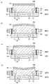
실시 형태에 따른 적재대(14)의 온도 제어에 의한 적재대(14)의 형상 제어의 일례에 대해서, 도 2 및 도 3을 참조하여 설명한다. 도 2 및 도 3은, 실시 형태에 따른 적재대(14)의 온도 제어의 일례를 도시하는 도면이다. 도 2 및 도 3의 나사(19)는, 제1 플레이트(18)의 외주에 형성된 제1 플레이트(18)를 관통하는 관통 구멍(19a)을 통해서, 제2 플레이트(16)의 외주의 상면에 형성된 나사 구멍(19b)과 나사 결합한다. 나사(19)에 의해 제1 플레이트(18)와 제2 플레이트(16)의 접촉면을 걸쳐서 제1 플레이트(18)와 제2 플레이트(16)를 나사 고정함으로써 제1 플레이트(18)와 제2 플레이트(16)를 체결한다. 또한, 제2 플레이트(16)에 관통 구멍을 형성하고, 제1 플레이트(18)의 하면에 나사 구멍을 형성해서 나사 고정해도 된다.An example of the shape control of the mounting table 14 by the temperature control of the mounting table 14 which concerns on embodiment is demonstrated with reference to FIG.2 and FIG.3. 2 and 3 are diagrams showing an example of temperature control of the mounting table 14 according to the embodiment. The
제1 플레이트(18)와 제2 플레이트(16)는, 나사(19)에 의해 견고하게 체결되어 있다. 이 때문에, 제1 플레이트(18) 또는 제2 플레이트(16)에 온도 변화가 생긴 경우, 제1 플레이트(18) 또는 제2 플레이트(16)에 열응력이 생긴다.The
예를 들어, 도 2의 (a)에 도시하는 바와 같이, 제1 유로(18f)에 흘리는 전열 매체를 0℃로 제어하여, 제1 플레이트(18)의 온도를 제어하고, 제2 유로(16f)에 흘리는 전열 매체를 -100℃로 제어하여, 제2 플레이트(16)의 온도를 제어한다. 이어서, 도 2의 (b)에 도시하는 바와 같이, 제1 유로(18f)에 흘리는 전열 매체의 온도는 0℃를 유지하면서, 제2 유로(16f)에 흘리는 전열 매체의 온도를 100℃로 제어해서 제2 플레이트(16)의 온도를 제어한다.For example, as shown in Fig. 2(a), the heat transfer medium flowing through the
이렇게 도 2의 (a)의 상태에서 도 2의 (b)의 상태로 이행시킨 경우, 제2 플레이트(16)는 -100℃에서 100℃로 온도가 변화하고, 제1 플레이트(18)는 0℃인 채로 온도는 변화하지 않았다. 이 때문에, 제2 플레이트(16)는 제1 플레이트(18)보다도 수직 방향 및 수평 방향으로 팽창한다. 제1 플레이트(18)와 제2 플레이트(16)는, 나사(19)에 의해 견고하게 체결되어 있다. 이 때문에, 제2 플레이트(16)의 수평 방향으로의 팽창이 방해되어, 제2 플레이트(16)에 열응력(압축 응력)이 생긴다. 또한, 이것에 수반하여, 제1 플레이트(18)에는 인장 응력이 생겨서, 정전 척(20) 및 제1 플레이트(18)가 기판 적재면(20a)측으로 오목 형상으로 변형된다.In this way, when the state of FIG. 2 (a) is transferred to the state of FIG. 2 (b), the temperature of the
이어서, 정전 척(20)을 기판 적재면(20a)측에 볼록 형상으로 변형시킬 경우의 온도 제어에 대해서, 도 3을 참조하여 설명한다. 도 3의 (a)에 도시하는 바와 같이, 제1 유로(18f)에 흘리는 전열 매체를 0℃로 제어하여, 제1 플레이트(18)의 온도를 제어하고, 제2 유로(16f)에 흘리는 전열 매체를 100℃로 제어하여, 제2 플레이트(16)의 온도를 제어한다. 이어서, 도 3의 (b)에 도시하는 바와 같이, 제1 유로(18f)에 흘리는 전열 매체의 온도는 0℃를 유지하면서, 제2 유로(16f)에 흘리는 전열 매체의 온도를 -100℃로 제어해서 제2 플레이트(16)의 온도를 제어한다.Next, temperature control when the
이렇게 도 3의 (a)의 상태에서 도 3의 (b)의 상태로 이행시킨 경우, 제2 플레이트(16)는 100℃에서 -100℃로 온도가 변화하고, 제1 플레이트(18)는 0℃인 채로 온도는 변화하지 않았다. 이 때문에, 제2 플레이트(16)는 제1 플레이트(18)보다도 수직 방향 및 수평 방향으로 수축한다. 제1 플레이트(18)와 제2 플레이트(16)는, 나사(19)에 의해 견고하게 체결되어 있다. 이 때문에, 제2 플레이트(16)의 수평 방향으로의 수축이 방해되어, 제2 플레이트(16)에 열응력(인장 응력)이 생긴다. 또한, 이것에 수반하여, 제1 플레이트(18)에는 압축 응력이 생겨서, 정전 척(20) 및 제1 플레이트(18)가 기판 적재면(20a)측으로 볼록 형상으로 변형된다. 이에 의해, 기판(W)의 휨에 맞춰서 적재대(14)를 기판(W)의 휨 방향으로 적극적으로 휘게 할 수 있다.In this way, when the state of FIG. 3 (a) is transferred to the state of FIG. 3 (b), the temperature of the
또한, 제1 플레이트(18)와 제2 플레이트(16)는, 나사(19)로 견고하게 체결되어 있기 때문에, 제1 플레이트(18)의 하면과 제2 플레이트(16)의 상면 사이에는, 견고한 마찰력이 발생되어 있다. 그러나, 제1 플레이트(18) 또는 제2 플레이트(16)의 온도 변화를 급속하게 행하면, 마찰력보다도 강한 인장 응력(또는 압축 응력)이 급속하게 발생하기 때문에, 미끄러짐이 생긴다. 이 때문에, 제1 플레이트(18) 또는 제2 플레이트(16)의 변형이 생기지 않는 경우가 있다. 따라서, 기판 적재면(20a)의 변형을 제어하기 위해서는, 제1 플레이트(18) 또는 제2 플레이트(16)의 온도 제어를, 강한 열응력이 발생하지 않는 범위에서 행하는 것이 바람직하다. 구체적으로는, 제1 플레이트(18)와 제2 플레이트(16)의 온도 변화의 차가, 3℃/분 이하로 되도록 승온 또는 강온하는 것이 바람직하다.In addition, since the
이와 같이, 실시 형태에서는, 제2 유로(16f)의 전열 매체의 온도를 제어함으로써, 적재대(14)의 변형을 적극적으로 제어할 수 있다. 예를 들어, 기판(W)과 동일한 방향으로 적재대(14)를 휘게 하고자 하는 경우, 기판(W)의 휨을 측정하여, 측정한 결과에 따라서 적재대(14)를 기판(W)의 휨 방향으로 적극적으로 휘게 할 수 있다.Thus, in embodiment, the deformation|transformation of the mounting table 14 can be controlled positively by controlling the temperature of the heat transfer medium of the
또한, 실시 형태에서는, 제1 유로(18f)의 전열 매체의 온도는 변화시키지 않았다. 즉, 제1 플레이트(18)의 온도를 프로세스에 적합한 온도로 고정한 채, 제2 플레이트(16)의 온도를 변화시킴으로써, 기판 적재면(20a)의 형상을 자유롭게 제어할 수 있다.In addition, in the embodiment, the temperature of the heat transfer medium of the
실시 형태에 따른 온도 제어 방법은, 기판(W)의 형상을 측정하는 공정과, 측정한 기판(W)의 형상에 기초하여, 제2 플레이트(16)의 제2 유로(16f)를 흐르는 전열 매체의 온도를 제어하는 공정을 갖는다. 이러한 온도 제어 방법에 의하면, 제1 플레이트(18)와 제2 플레이트(16) 양쪽에 온도 조절 기구를 마련함으로써, 기판(W)의 형상에 따라서 적재대(14)의 변형을 적극적으로 제어할 수 있다. 이에 의해, 기판(W)의 휨 방향으로 정전 척(20)의 기판 적재면(20a)을 변형시켜, 기판(W)과 정전 척(20)의 밀착성을 높여서, 기판(W)의 온도의 제어성을 높일 수 있다. 이에 의해, 기판의 면내 온도 분포를 작게 하여, 기판(W)에의 에칭 특성(에칭 레이트 등)을 향상시킬 수 있다. 또한, 기판(W)의 형상은, 반송 암에 적재된 기판(W)의 휨을 레이저광의 반사광의 상태로부터 측정해도 되고, 반송 암에 적재된 기판(W)의 접촉면의 상태를 측정함으로써 추정해도 되고, 다른 공지된 방법으로 측정해도 된다.The temperature control method according to the embodiment includes the steps of measuring the shape of the substrate W, and a heat transfer medium flowing through the
[적재대의 형상 제어(다른 예)][Controlling the shape of the loading platform (another example)]
이어서, 실시 형태에 따른 적재대(14)의 온도 제어에 의한 형상 제어의 다른 예에 대해서, 도 4 및 도 5를 참조하여 설명한다. 도 4 및 도 5는, 실시 형태에 따른 적재대(14)의 온도 제어의 다른 예를 도시하는 도면이다.Next, another example of the shape control by the temperature control of the mounting table 14 which concerns on embodiment is demonstrated with reference to FIG.4 and FIG.5. 4 and 5 are diagrams showing another example of temperature control of the mounting table 14 according to the embodiment.
예를 들어, 도 4의 (a)에 도시하는 바와 같이, 제1 유로(18f)에 흘리는 전열 매체를 40℃로 제어하여, 제1 플레이트(18)의 온도를 제어하고, 제2 유로(16f)에 흘리는 전열 매체를 40℃로 제어하여, 제2 플레이트(16)의 온도를 제어한다. 이때, 기판 적재면(20a)은 평탄한 상태이다. 이어서 도 4의 (b)에 도시하는 바와 같이, 제1 유로(18f)에 흘리는 전열 매체를 20℃로 제어하여, 제1 플레이트(18)의 온도를 제어하고, 제2 유로(16f)에 흘리는 전열 매체를 80℃로 제어하여, 제2 플레이트(16)의 온도를 제어한다. 이어서, 도 4의 (c)에 도시하는 바와 같이, 제2 유로(16f)에 흘리는 전열 매체의 온도는 80℃인 채로, 제1 유로(18f)에 흘리는 전열 매체의 온도를 40℃로 제어해서 제1 플레이트(18)를 온도 조절한다. 그리고, 도 4의 (d)에 도시하는 바와 같이, 제1 유로(18f)에 흘리는 전열 매체의 온도는 40℃인 채로, 제2 유로(16f)에 흘리는 전열 매체의 온도를 40℃로 제어해서 제2 플레이트(16)를 온도 조절한다.For example, as shown in Fig. 4A, the heat transfer medium flowing through the
도 4의 (a)에 도시하는 바와 같이, 제1 플레이트(18)와 제2 플레이트(16)는 동일한 온도로 제어되어 있다. 또한, 이때 기판 적재면(20a)은 평탄한 상태이다. 이 상태로부터, 도 4의 (b)에 도시하는 바와 같이, 제1 플레이트(18)의 온도를 40℃에서 20℃로 내린다. 또한 제2 플레이트(16)의 온도를 40℃에서 80℃로 높인다. 이에 의해, 제1 플레이트(18)는 수축하고, 제2 플레이트(16)는 팽창한다. 또한, 제1 플레이트(18)와 제2 플레이트(16)는, 나사(19)에 의해 견고하게 체결되어 있다. 이 때문에, 제2 플레이트(16)의 수평 방향으로의 팽창이 방해되어, 제2 플레이트(16)에 열응력(압축 응력)이 생긴다. 또한, 이것에 수반하여, 제1 플레이트(18)에는 인장 응력이 생긴다. 또한, 제1 플레이트(18)의 수평 방향으로의 수축이 방해되어, 제1 플레이트(18)에 열응력(인장 응력)이 생긴다. 이에 의해, 정전 척(20) 및 제1 플레이트(18)가 기판 적재면(20a)측으로 오목 형상으로 변형된다.As shown in Fig. 4A, the
이어서, 도 4의 (c)에 도시하는 바와 같이, 제2 유로(16f)에 흘리는 전열 매체의 온도는 80℃인 채로, 제1 유로(18f)에 흘리는 전열 매체의 온도를 40℃로 제어해서 제1 플레이트(18)를 온도 조절한다.Next, as shown in Fig. 4(c), the temperature of the heat transfer medium flowing through the
이 경우, 제1 플레이트(18)는 도 4의 (b)에 도시한 상태보다도 높은 온도로 되기 때문에, 제1 플레이트(18)는 팽창한다. 제1 플레이트(18)와 제2 플레이트(16)는, 나사(19)에 의해 견고하게 체결되어 있다. 이 때문에, 제1 플레이트(18)의 수평 방향으로의 팽창이 방해되어, 제1 플레이트(18)에 열응력(압축 응력)이 생긴다. 이에 의해, 정전 척(20) 및 제1 플레이트(18)가 기판 적재면(20a)측으로 볼록 형상으로 변형된다. 도 4의 (b)에 도시한 상태에서, 정전 척(20) 및 제1 플레이트(18)가 기판 적재면(20a)측으로 오목 형상으로 변형되어 있기 때문에, 도 4의 (c)에 도시한 상태에서는, 기판 적재면(20a)은 대략 평탄한 상태로 된다.In this case, since the temperature of the
이어서, 도 4의 (d)에 도시하는 바와 같이, 제1 유로(18f)에 흘리는 전열 매체의 온도는 40℃인 채로, 제2 유로(16f)에 흘리는 전열 매체의 온도를 40℃로 제어해서 제2 플레이트(16)의 온도를 제어한다.Next, as shown in Fig. 4(d), the temperature of the heat transfer medium flowing through the
이 경우, 제2 플레이트(16)는, 도 4의 (c)에 도시한 상태보다도 낮은 온도가 되기 때문에, 제2 플레이트(16)는 수축한다. 제1 플레이트(18)와 제2 플레이트(16)는, 나사(19)에 의해 견고하게 체결되어 있다. 이 때문에, 제2 플레이트(16)의 수평 방향으로의 수축이 방해되어, 제2 플레이트(16)에 열응력(인장 응력)이 생긴다. 또한, 이것에 수반하여, 제1 플레이트(18)에는 압축 응력이 생겨서, 정전 척(20) 및 제1 플레이트(18)가 기판 적재면(20a)측으로 볼록 형상으로 변형된다.In this case, since the temperature of the
이어서, 정전 척(20)을 기판 적재면(20a)측으로 오목 형상으로 변형시킬 경우의 온도 제어의 일례에 대해서, 도 5를 참조하여 설명한다. 도 5의 (a)에 도시하는 바와 같이, 제1 유로(18f)에 흘리는 전열 매체를 40℃로 제어하여, 제1 플레이트(18)의 온도를 제어하고, 제2 유로(16f)에 흘리는 전열 매체를 40℃로 제어하여, 제2 플레이트(16)의 온도를 제어한다. 이때, 기판 적재면(20a)은 평탄한 상태이다. 이어서, 도 5의 (b)에 도시하는 바와 같이, 제1 유로(18f)에 흘리는 전열 매체를 80℃로 제어하여, 제1 플레이트(18)의 온도를 제어하고, 제2 유로(16f)에 흘리는 전열 매체를 0℃로 제어하여, 제2 플레이트(16)의 온도를 제어한다. 이어서, 도 5의 (c)에 도시하는 바와 같이, 제2 유로(16f)에 흘리는 전열 매체의 온도는 0℃인 채로, 제1 유로(18f)에 흘리는 전열 매체의 온도를 40℃로 제어해서 제1 플레이트(18)의 온도를 제어한다. 그리고, 도 5의 (d)에 도시하는 바와 같이, 제1 유로(18f)에 흘리는 전열 매체의 온도는 40℃인 채로, 제2 유로(16f)에 흘리는 전열 매체의 온도를 40℃로 제어해서 제2 플레이트(16)의 온도를 제어한다.Next, an example of temperature control when the
도 5의 (a)에 도시하는 바와 같이, 제1 플레이트(18)와 제2 플레이트(16)는 동일한 온도로 제어되어 있다. 또한, 기판 적재면(20a)은 평탄한 상태이다. 이 상태로부터, 도 5의 (b)에 도시하는 바와 같이, 제1 플레이트(18)의 온도를 40℃에서 80℃로 높인다. 또한 제2 플레이트(16)의 온도를 40℃에서 0℃로 내린다. 제1 플레이트(18)는 팽창하고, 제2 플레이트(16)는 수축한다. 또한, 제1 플레이트(18)와 제2 플레이트(16)는, 나사(19)에 의해 견고하게 체결되어 있다. 이 때문에, 제2 플레이트(16)의 수평 방향으로의 수축이 방해되어, 제2 플레이트(16)에 열응력(인장 응력)이 생긴다. 또한, 이것에 수반하여, 제1 플레이트(18)에는 압축 응력이 생긴다. 또한, 제1 플레이트(18)의 수평 방향으로의 팽창이 방해되어, 제1 플레이트(18)에 열응력(압축 응력)이 생긴다. 이에 의해, 정전 척(20) 및 제1 플레이트(18)가 기판 적재면(20a)측으로 볼록 형상으로 변형된다.As shown in Fig. 5A, the
이어서, 도 5의 (c)에 도시하는 바와 같이, 제2 유로(16f)에 흘리는 전열 매체의 온도는 0℃인 채로, 제1 유로(18f)에 흘리는 전열 매체의 온도를 40℃로 제어해서 제1 플레이트(18)의 온도를 제어한다.Next, as shown in Fig. 5(c), the temperature of the heat transfer medium flowing through the
이 경우, 제1 플레이트(18)는 도 5의 (b)에 도시한 상태보다도 낮은 온도로 되기 때문에, 제1 플레이트(18)는 수축한다. 제1 플레이트(18)와 제2 플레이트(16)는, 나사(19)에 의해 견고하게 체결되어 있다. 이 때문에, 제1 플레이트(18)의 수평 방향으로의 수축이 방해되어, 제1 플레이트(18)에 열응력(인장 응력)이 생긴다. 이에 의해, 정전 척(20) 및 제1 플레이트(18)가 기판 적재면(20a)측으로 오목 형상으로 변형된다. 도 5의 (b)에 도시한 상태에서, 정전 척(20) 및 제1 플레이트(18)가 기판 적재면(20a)측으로 볼록 형상으로 변형되어 있기 때문에, 도 5의 (c)에 도시한 상태에서는 기판 적재면(20a)은 대략 평탄한 상태로 된다.In this case, since the temperature of the
이어서, 도 5의 (d)에 도시하는 바와 같이, 제1 유로(18f)에 흘리는 전열 매체의 온도는 40℃인 채로, 제2 유로(16f)에 흘리는 전열 매체의 온도를 40℃로 제어해서 제2 플레이트(16)의 온도를 제어한다.Next, as shown in Fig. 5(d), the temperature of the heat transfer medium flowing through the
이 경우, 제2 플레이트(16)는 도 5의 (c)에 도시한 상태보다도 높은 온도가 되기 때문에, 제2 플레이트(16)는 팽창한다. 제1 플레이트(18)와 제2 플레이트(16)는, 나사(19)에 의해 견고하게 체결되어 있다. 이 때문에, 제2 플레이트(16)의 수평 방향으로의 팽창이 방해되어, 제2 플레이트(16)에 열응력(압축 응력)이 생긴다. 이것에 수반하여, 제1 플레이트(18)에 인장 응력이 생겨서, 정전 척(20) 및 제1 플레이트(18)가 기판 적재면(20a)측으로 오목 형상으로 변형된다.In this case, since the temperature of the
또한, 도 4의 (b)에서, 기판 적재면(20a)을 오목형으로 하기 위해서, 제2 플레이트(16)의 온도를 높이고, 제1 플레이트(18)의 온도를 낮추었다. 그러나, 제1 플레이트(18) 및 제2 플레이트(16)의 양쪽 온도를 높여서 오목 형상으로 해도 된다. 예를 들어, 제1 플레이트(18)의 온도를 40℃에서 60℃로 높이고, 제2 플레이트(16)의 온도를 40℃에서 80℃로 높인다. 이 경우, 제2 플레이트(16)의 온도 변화가 제1 플레이트(18)의 온도 변화보다도 크기 때문에, 제2 플레이트(16)쪽이 크게 팽창한다. 이 때문에, 제2 플레이트(16)의 수평 방향으로의 팽창이 방해되어, 제2 플레이트(16)에 열응력(압축 응력)이 생긴다. 또한, 이것에 수반하여, 제1 플레이트(18)에는 인장 응력이 생긴다. 이에 의해, 기판 적재면(20a)을 오목 형상으로 할 수 있다. 또한, 제1 플레이트(18)의 온도를 변화시키지 않고, 제2 플레이트(16)의 온도만을 높여도 되고, 제2 플레이트(16)의 온도를 변화시키지 않고, 제1 플레이트(18)의 온도만을 내려도 된다.In addition, in FIG.4(b), in order to make the board|
또한, 기판 적재면(20a)을 볼록형으로 하기 위해서, 제1 플레이트(18)의 온도 변화가 제2 플레이트(16)의 온도 변화보다도 커지도록, 제1 플레이트(18) 및 제2 플레이트(16)의 온도를 상승시켜도 된다. 제1 플레이트(18)의 온도를 변화시키지 않고, 제2 플레이트(16)의 온도만을 내려도 되고, 제2 플레이트(16)의 온도를 변화시키지 않고, 제1 플레이트(18)의 온도만을 높여도 된다.Moreover, in order to make the board|
이와 같이, 실시 형태에서는, 제1 유로(18f) 및/또는 제2 유로(16f)의 전열 매체의 온도를 제어함으로써, 적재대(14)의 변형을 적극적으로 제어할 수 있다. 즉, 제1 플레이트(18)와 제2 플레이트(16)의 온도 변화를 조합한다. 이에 의해, 제1 플레이트(18)와 제2 플레이트(16)의 온도를 초기 상태(도 4의 (a) 또는 도 5의 (a))와 동일한 온도로 제어해도, 기판 적재면(20a)의 형상을 변화시킬 수 있다(도 4의 (d) 또는 도 5의 (d)). 또한, 도 4 및 도 5의 예에서는, 초기 상태에서의 기판 적재면(20a)의 형상은 평탄하게 했지만, 오목형 또는 볼록형이어도 된다. 즉, 초기 상태의 기판 적재면(20a)의 형상에 따라, 제1 플레이트(18)와 제2 플레이트(16)의 온도 변화를 행함으로써, 제1 플레이트(18)와 제2 플레이트(16)의 온도에 구애되지 않고 기판 적재면(20a)의 형상을 임의로 변화시킬 수 있다.Thus, in embodiment, the deformation|transformation of the mounting table 14 can be positively controlled by controlling the temperature of the heat transfer medium of the
이상으로 설명한 제1 유로(18f)에 흘리는 전열 매체와 제2 유로(16f)에 흘리는 전열 매체의 온도 제어에서는 다양한 제어가 가능하다. 예를 들어, 제어부(80)는, 제1 플레이트(18)와 제2 플레이트(16)가 동일한 타이밍에 동일한 온도로 되도록 제1 유로(18f)에 흘리는 전열 매체 및 제2 유로(16f)에 흘리는 전열 매체의 온도를 제어해도 된다. 이에 의하면, 제1 플레이트(18)와 제2 플레이트(16)를 동일한 타이밍에 동일한 온도로 할 수 있다. 이 때문에, 제1 플레이트(18)와 제2 플레이트(16)에 생기는 열응력의 차에 의해 적재대(14)에 변형이 생하지 않는다. 또한, 이러한 제어만을 행하는 경우에는, 제1 칠러 유닛(21a)과 제2 칠러 유닛(21b)은 동일한 칠러 유닛이어도 된다. 즉, 제1 칠러 유닛(21a)을 제1 유로(18f) 및 제2 유로(16f)에 접속하고, 제2 칠러 유닛(21b)은 마련하지 않아도 된다.Various controls are possible in the temperature control of the heat transfer medium flowing through the
[온도 제어 방법][Temperature control method]
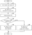
이어서, 실시 형태에 따른 온도 제어 방법에 대해서 도 6을 참조하면서 설명한다. 도 6은, 실시 형태에 따른 온도 제어 방법의 일례를 도시하는 도면이다.Next, a temperature control method according to an embodiment will be described with reference to FIG. 6 . 6 is a diagram illustrating an example of a temperature control method according to an embodiment.
본 처리가 개시되면, 제어부(80)는 기판 적재면(20a)의 형상 정보를 취득한다(스텝 S1). 기판 적재면(20a)의 형상 정보는, 센서에 의한 측정에 의해 취득해도 된다. 또한, 기억부에 기억한 제1 플레이트(18) 및 제2 플레이트(16)의 온도 변화의 이력과, 제1 플레이트(18) 및 제2 플레이트(16)의 온도 변화와 제1 플레이트(18)의 형상 변화의 상관관계를 나타내는 정보를 참조하여 취득해도 된다.When this process is started, the
이어서, 제어부(80)는 제1 플레이트(18)의 온도 및 제2 플레이트(16)의 온도를 취득한다(스텝 S2). 제1 플레이트(18)의 온도 및 제2 플레이트(16)의 온도는 각각, 제1 유로(18f)에 흘리는 전열 매체의 온도 및 제2 유로(16f)에 흘리는 전열 매체의 온도이어도 된다. 또한, 제1 플레이트(18) 및 제2 플레이트(16)에 각각 마련된 온도 센서에 의해 측정한 온도이어도 된다.Next, the
이어서, 제어부(80)는 기판(W)의 휨 정보를 취득한다(스텝 S3). 기판(W)의 휨 정보는, 기판 처리 장치(1)와는 다른 측정 장치에서 측정한 정보를 사용해도 되고, 기판 처리 장치(1)의 내부에 마련한 측정부에서 측정한 정보를 사용해도 된다.Next, the
이어서, 제어부(80)는, 적재대(14)(기판 적재면(20a))의 형상을 변화시킬 것인지 여부를 판정한다(스텝 S4). 적재대(14)의 형상을 변화시킬 것인지 여부는, 스텝 S1에서 취득한 기판 적재면(20a)의 형상 정보와, 스텝 S3에서 취득한 기판(W)의 휨 정보에 기초하여 판정해도 된다.Next, the
스텝 S4에서, 제어부(80)는, 적재대(14)의 형상을 변화시키지 않는다고 판정 한 경우, 제1 플레이트(18)와 제2 플레이트(16)를 동일한 온도로 제어하고(스텝 S5), 본 처리를 종료한다. 즉, 제1 유로(18f)에 흘리는 전열 매체의 온도 및 제2 유로(16f)에 흘리는 전열 매체의 온도를 동일 온도 또는 플라스마로부터의 입열을 고려한 소정의 온도로 제어하여, 제1 플레이트(18)와 제2 플레이트(16)에 온도 차가 생기지 않도록 제어한다.In step S4, when it is determined that the shape of the mounting table 14 is not changed, the
스텝 S4에서, 제어부(80)는, 적재대(14)의 형상을 변화시킨다고 판정한 경우, 제1 플레이트(18) 및/또는 제2 플레이트(16)의 온도를 제어하고(스텝 S6), 본 처리를 종료한다. 스텝 S6 후에, 기판 적재면(20a)이 원하는 형상으로 변형되었는지 여부를, 센서를 사용해서 확인해도 된다.In step S4, when it is determined that the shape of the mounting table 14 is to be changed, the
[형상 측정][Measurement of shape]
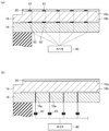
이어서, 제1 플레이트(18)의 형상을 측정하고, 측정 결과에 기초하여 제1 유로(18f)에 흘리는 전열 매체 및/또는 제2 유로(16f)에 흘리는 전열 매체의 온도를 제어하는 예에 대해서, 도 7을 참조하여 설명한다. 도 7은, 실시 형태에 따른 복수의 센서의 배치 예를 도시하는 도면이다.Next, about an example in which the shape of the
실시 형태에 따른 적재대(14)는, 제1 플레이트(18)의 형상을 측정하는 복수의 센서를 가져도 된다. 도 7의 (a)에 도시하는 바와 같이, 복수의 센서의 일례로서, 복수의 스트레인 게이지(81, 82)가 적재대(14)에 마련되어 있다. 도 7의 (a)의 예에서는, 복수의 스트레인 게이지(81)가 제1 플레이트(18)의 상면(18a)(정전 척(20)의 하면)에 첩부되어 있다. 또한, 복수의 스트레인 게이지(82)가 제1 플레이트(18)의 하면(18b)에 첩부되어 있다. 복수의 스트레인 게이지(81)는, 제1 플레이트(18)와 정전 척(20) 사이가 도시하지 않은 접착층 내에 배치되어도 된다. 복수의 스트레인 게이지(81, 82)로 측정한 복수의 수축 및 팽창의 값은, 제어부(80)에 보내진다. 제어부(80)는, 측정한 복수의 수축 및 팽창의 값으로부터, 제1 플레이트(18)의 형상을 측정한다. 정전 척(20)의 표면 형상은 제1 플레이트(18)의 형상에 따라 변화하기 때문에, 제1 플레이트(18)의 형상을 측정함으로써 정전 척(20)의 표면 형상을 추정할 수 있다.The mounting table 14 according to the embodiment may have a plurality of sensors that measure the shape of the
제어부(80)는, 제1 플레이트(18)의 제1 유로(18f)의 전열 매체의 온도, 및/또는 제2 플레이트(16)의 제2 유로(16f)의 전열 매체의 온도를, 측정한 제1 플레이트(18)의 형상에 맞추도록 제어한다.The
이와 같이, 복수의 스트레인 게이지(81, 82)의 측정값으로부터 추정한 제1 플레이트(18)의 표면 형상에 맞추어, 제1 플레이트(18) 및/또는 제2 플레이트(16)의 온도를 피드백한다. 이에 의해, 실시간으로 적어도 어느 것의 플레이트의 온도를 제어함으로써, 액티브하게 제1 플레이트(18)의 표면 형상(정전 척(20)의 표면 형상)을 제어할 수 있다.In this way, the temperature of the
단, 복수의 스트레인 게이지(81, 82)의 배치는 이것에 한정되지 않는다. 복수의 스트레인 게이지(81, 82)는, 제1 플레이트(18)의 상면(18a) 및 하면(18b)의 적어도 한쪽에 첩부해도 되고, 정전 척(20)의 하면에 첩부해도 된다. 복수의 스트레인 게이지(81, 82)는, 제1 플레이트의 형상을 측정하는 복수의 변형 센서의 일례이며, 복수의 변형 센서는, 로드 셀이어도 된다.However, the arrangement of the plurality of
도 7의 (b)에 도시하는 바와 같이, 복수의 센서의 일례로서, 복수의 레이저 간섭계(83)를 적재대(14)에 마련해도 된다. 복수의 레이저 간섭계(83)는, 제2 플레이트(16)의 하방에 마련되어, 제2 플레이트(16)를 관통하는 관통 구멍(16a)에 통과시킨 레이저광을 제1 플레이트(18)의 하면(18b)에 조사한다. 복수의 레이저 간섭계(83)는, 하면(18b)에서 반사한 광을 수광한 시간에 기초하여 제1 플레이트(18)의 하면까지의 거리를 측정한다. 제어부(80)는, 복수의 레이저 간섭계(83)로부터 취득한 거리에 기초하여, 제1 플레이트(18)의 형상을 측정한다. 정전 척(20)의 표면 형상은, 제1 플레이트(18)의 형상의 변화에 추종하고 있기 때문에, 제1 플레이트(18)의 형상을 측정함으로써, 정전 척(20)의 표면 형상을 추정할 수 있다.As shown in FIG. 7B , as an example of the plurality of sensors, a plurality of
제어부(80)는, 제1 플레이트(18)의 제1 유로(18f)의 전열 매체의 온도, 및/또는 제2 플레이트(16)의 제2 유로(16f)의 전열 매체의 온도를, 측정한 제1 플레이트(18)의 형상에 맞추도록 제어한다.The
이와 같이, 복수의 레이저 간섭계(83)의 측정값으로부터 추정한 제1 플레이트(18)의 표면 형상에 맞추어, 제1 플레이트(18) 및/또는 제2 플레이트(16)의 온도를 피드백한다. 이에 의해, 실시간으로 적어도 어느 것의 플레이트의 온도를 제어함으로써, 액티브하게 제1 플레이트(18)의 표면 형상을 제어할 수 있다.In this way, the temperature of the
이때, 포커서 등의 조사 기기는 기준으로 고정해 두고, 그 측장의 변화가 정전 척(20)의 하면의 변화로 된다. 이 변화를 피드백해서 제1 플레이트(18)의 제1 유로(18f)의 전열 매체의 온도, 및/또는 제2 플레이트(16)의 제2 유로(16f)의 전열 매체의 온도를 실시간으로 제어함으로써, 액티브하게 정전 척(20)의 표면 형상을 제어 가능하게 한다.At this time, an irradiation device such as a focuser is fixed as a reference, and a change in the length becomes a change in the lower surface of the
적재대(14)의 온도 제어 방법은, 제1 플레이트(18)의 형상을 측정하는 공정과, 측정한 제1 플레이트(18)의 형상에 기초하여, 제1 플레이트(18)의 온도 조절 기구 및/또는 제2 플레이트(16)의 온도 조절 기구를 제어하는 공정을 포함한다.The temperature control method of the mounting table 14 includes a process of measuring the shape of the
이상의 설명에서는, 측정한 제1 플레이트(18)의 형상에 기초하여, 실시간으로 제1 플레이트(18)의 온도 조절 기구 및/또는 제2 플레이트(16)의 온도 조절 기구를 제어하였다. 그러나, 이것에 한정되지 않고, 제1 플레이트(18)의 형상을 측정하지 않아도 된다. 예를 들어, 기억부에 기억한 제1 플레이트(18) 및 제2 플레이트(16)의 온도 변화의 이력과, 제1 플레이트(18) 및 제2 플레이트(16)의 온도 변화와 제1 플레이트의 형상 변화의 상관 관계를 나타내는 정보를 참조하여, 제1 플레이트(18)의 형상을 추정해도 된다.In the above description, the temperature control mechanism of the
제1 플레이트(18) 및 제2 플레이트(16)의 온도 변화와 제1 플레이트(18)의 형상 변화의 상관 관계를 나타내는 정보는, 제1 플레이트(18)의 형상 변화와 제1 온도 조절 기구 및 제2 온도 조절 기구의 온도의 관계를 측정하여, 기억부에 미리 기억해도 된다. 기억부는, 제어부(80)의 메모리이어도 된다. 제1 플레이트(18)의 형상과 온도 변화의 상관 관계를 나타내는 정보는, 제1 플레이트(18)의 형상을 편평하게 하기 위한 제1 플레이트(18)의 형상과 온도 변화의 상관 관계를 나타내는 정보이어도 된다. 또한, 제1 플레이트(18)의 형상을 오목형으로 하기 위한 제1 플레이트의 형상과 온도 변화의 상관계를 나타내는 정보이어도 된다. 또한, 제1 플레이트(18)의 형상을 볼록형으로 하기 위한 제1 플레이트(18)의 형상과 온도 변화의 상관 관계를 나타내는 정보이어도 된다.The information indicating the correlation between the change in the temperature of the
이상으로 설명한 온도 제어 방법에 의하면, 적재대(14)의 변형을 제어할 수 있다. 금회 개시된 일 실시 형태에 따른 기판 처리 장치(1), 적재대(14) 및 온도 제어 방법은, 모든 점에서 예시이며 제한적인 것이 아니라고 생각되어야 한다. 상기 실시 형태는, 첨부의 청구범위 및 그 주지를 일탈하지 않고, 다양한 형태로 변형 및 개량이 가능하다. 상기 복수의 실시 형태에 기재된 사항은, 모순되지 않는 범위에서 다른 구성도 취할 수 있으며, 또한 모순되지 않는 범위에서 조합할 수 있다.According to the temperature control method demonstrated above, the deformation|transformation of the mounting table 14 can be controlled. It should be considered that the
예를 들어, 기판 처리 장치의 일례로서 플라스마 처리 장치를 들어 설명했지만, 기판 처리 장치는, 기판에 소정의 처리(예를 들어, 성막 처리, 에칭 처리 등)를 실시하는 장치이면 되며, 플라스마 처리 장치에 한정되는 것은 아니다.For example, although a plasma processing apparatus has been described as an example of a substrate processing apparatus, the substrate processing apparatus may be an apparatus that performs a predetermined process (eg, film forming process, etching process, etc.) on a substrate, and a plasma processing apparatus is not limited to
또한, 기판 처리 장치는, 에칭 장치, 성막 장치, 애싱 장치, 도핑 장치 등이어도 된다. 예를 들어, 기판 처리 장치는, 스퍼터링법에 의한 ITO의 성막 장치나, MOCVD법에 의한 금속 함유막 성막 장치이어도 된다.In addition, an etching apparatus, a film-forming apparatus, an ashing apparatus, a doping apparatus, etc. may be sufficient as a substrate processing apparatus. For example, the substrate processing apparatus may be an ITO film forming apparatus by a sputtering method or a metal-containing film forming apparatus by an MOCVD method.
본 개시의 기판 처리 장치는, Atomic Layer Deposition(ALD) 장치, Capacitively Coupled Plasma(CCP), Inductively Coupled Plasma(ICP), Radial Line Slot Antenna(RLSA), Electron Cyclotron Resonance Plasma(ECR), Helicon Wave Plasma(HWP)의 어느 타입의 장치이어도 적용 가능하다.The substrate processing apparatus of the present disclosure is an Atomic Layer Deposition (ALD) apparatus, Capacitively Coupled Plasma (CCP), Inductively Coupled Plasma (ICP), Radial Line Slot Antenna (RLSA), Electron Cyclotron Resonance Plasma (ECR), Helicon Wave Plasma ( Any type of device of HWP) is applicable.
Claims (15)
상기 적재대는,
제1 플레이트와,
상기 제1 플레이트의 온도를 제어하는 제1 온도 조절 기구와,
상기 제1 플레이트의 하부에 배치되는 제2 플레이트와,
상기 제2 플레이트의 온도를 제어하는 제2 온도 조절 기구와,
상기 제1 플레이트와 상기 제2 플레이트를 체결하는 체결 부재
를 포함하는 기판 처리 장치.It is a substrate processing apparatus having a mounting table for loading a substrate,
The loading stand,
a first plate;
a first temperature control mechanism for controlling the temperature of the first plate;
a second plate disposed under the first plate;
a second temperature control mechanism for controlling the temperature of the second plate;
Fastening member for fastening the first plate and the second plate
A substrate processing apparatus comprising a.
상기 제어부는,
상기 제1 플레이트와 상기 제2 플레이트가 동일한 타이밍에 동일한 온도로 되도록 상기 제1 온도 조절 기구 및 상기 제2 온도 조절 기구를 제어하는, 기판 처리 장치.The method according to any one of claims 1 to 5, comprising a control unit for controlling the first temperature control mechanism and the second temperature control mechanism,
The control unit is
The substrate processing apparatus which controls the said 1st temperature control mechanism and the said 2nd temperature control mechanism so that the said 1st plate and the said 2nd plate may become the same temperature at the same timing.
상기 제어부는,
상기 제1 플레이트의 온도를 일정하게 한 채, 상기 제2 플레이트의 온도를 변화시키도록 상기 제1 온도 조절 기구 및 상기 제2 온도 조절 기구를 제어하는, 기판 처리 장치.The method according to any one of claims 1 to 5, comprising a control unit for controlling the first temperature control mechanism and the second temperature control mechanism,
The control unit is
The substrate processing apparatus which controls the said 1st temperature regulating mechanism and the said 2nd temperature regulating mechanism so that the temperature of the said 2nd plate may be changed with the temperature of the said 1st plate being constant.
상기 제1 플레이트의 온도를 제어하는 제1 온도 조절 기구와,
상기 제1 플레이트의 하부에 배치되는 제2 플레이트와,
상기 제2 플레이트의 온도를 제어하는 제2 온도 조절 기구와,
상기 제1 플레이트와 상기 제2 플레이트를 체결하는 체결 부재
를 포함하는 적재대.a first plate;
a first temperature control mechanism for controlling the temperature of the first plate;
a second plate disposed under the first plate;
a second temperature control mechanism for controlling the temperature of the second plate;
Fastening member for fastening the first plate and the second plate
A loading stand that includes.
(a) 상기 적재대에 적재하는 기판의 형상을 측정하는 공정과,
(b) 측정한 상기 기판의 형상에 기초하여, 상기 제1 온도 조절 기구 또는 상기 제2 온도 조절 기구를 제어하는 공정
을 포함하는 온도 제어 방법.A first plate, a first temperature control mechanism for controlling the temperature of the first plate, a second plate disposed under the first plate, and a second temperature control mechanism for controlling the temperature of the second plate; , A method of controlling the temperature of a loading table including a fastening member for fastening the first plate and the second plate,
(a) measuring the shape of the substrate to be loaded on the mounting table;
(b) The process of controlling the said 1st temperature control mechanism or the said 2nd temperature control mechanism based on the measured shape of the said board|substrate
A temperature control method comprising a.
Applications Claiming Priority (2)
| Application Number | Priority Date | Filing Date | Title |
|---|---|---|---|
| JP2020081397A JP7301021B2 (en) | 2020-05-01 | 2020-05-01 | SUBSTRATE PROCESSING APPARATUS, PLACEMENT STAND, AND TEMPERATURE CONTROL METHOD |
| JPJP-P-2020-081397 | 2020-05-01 |
Publications (1)
| Publication Number | Publication Date |
|---|---|
| KR20210134503A true KR20210134503A (en) | 2021-11-10 |
Family
ID=78243081
Family Applications (1)
| Application Number | Title | Priority Date | Filing Date |
|---|---|---|---|
| KR1020210051048A KR20210134503A (en) | 2020-05-01 | 2021-04-20 | Substrate processing apparatus, stage, and temperature control method |
Country Status (5)
| Country | Link |
|---|---|
| US (1) | US11626818B2 (en) |
| JP (2) | JP7301021B2 (en) |
| KR (1) | KR20210134503A (en) |
| CN (1) | CN113594016A (en) |
| TW (1) | TW202147504A (en) |
Citations (2)
| Publication number | Priority date | Publication date | Assignee | Title |
|---|---|---|---|---|
| JP2000021962A (en) | 1998-07-03 | 2000-01-21 | Hitachi Ltd | Electrostatic chuck device |
| JP2005072286A (en) | 2003-08-25 | 2005-03-17 | Kyocera Corp | Electrostatic chuck |
Family Cites Families (16)
| Publication number | Priority date | Publication date | Assignee | Title |
|---|---|---|---|---|
| JPH06302550A (en) * | 1993-04-13 | 1994-10-28 | Hitachi Ltd | Semiconductor manufacturing device |
| US5835334A (en) * | 1996-09-30 | 1998-11-10 | Lam Research | Variable high temperature chuck for high density plasma chemical vapor deposition |
| JP2000124299A (en) | 1998-10-16 | 2000-04-28 | Hitachi Ltd | Manufacture of semiconductor device and semiconductor manufacturing apparatus |
| JP2002009064A (en) * | 2000-06-21 | 2002-01-11 | Hitachi Ltd | Processing device for sample and processing method therefor |
| JP2003224180A (en) * | 2002-01-28 | 2003-08-08 | Kyocera Corp | Wafer support member |
| JP2007317772A (en) | 2006-05-24 | 2007-12-06 | Shinko Electric Ind Co Ltd | Electrostatic chuck device |
| JP2009218536A (en) | 2008-03-13 | 2009-09-24 | Seiko Epson Corp | Manufacturing apparatus of substrate heater and electro-optical device |
| JP2010182866A (en) | 2009-02-05 | 2010-08-19 | Nikon Corp | Electrostatic attraction holding device, aligner, exposure method, and method of manufacturing device |
| JP5357561B2 (en) | 2009-02-13 | 2013-12-04 | 信越化学工業株式会社 | Manufacturing method of semiconductor wafer with uniform surface polishing |
| JP5434636B2 (en) | 2010-01-29 | 2014-03-05 | 住友電気工業株式会社 | Substrate holder with electrostatic chuck |
| JP5496791B2 (en) * | 2010-06-29 | 2014-05-21 | シャープ株式会社 | Plasma processing equipment |
| JP6196095B2 (en) * | 2013-08-07 | 2017-09-13 | 日本特殊陶業株式会社 | Electrostatic chuck |
| US10195887B2 (en) | 2014-06-19 | 2019-02-05 | Sharp Kabushiki Kaisha | Transparent film, printed matter, printing device, and printing unit |
| JP6655310B2 (en) * | 2015-07-09 | 2020-02-26 | 株式会社日立ハイテクノロジーズ | Plasma processing equipment |
| KR102644272B1 (en) | 2016-10-31 | 2024-03-06 | 삼성전자주식회사 | electrostatic chuck assembly |
| JP7090465B2 (en) | 2018-05-10 | 2022-06-24 | 東京エレクトロン株式会社 | Mounting table and plasma processing equipment |
-
2020
- 2020-05-01 JP JP2020081397A patent/JP7301021B2/en active Active
-
2021
- 2021-04-20 TW TW110114121A patent/TW202147504A/en unknown
- 2021-04-20 KR KR1020210051048A patent/KR20210134503A/en active Search and Examination
- 2021-04-23 CN CN202110441064.5A patent/CN113594016A/en active Pending
- 2021-04-26 US US17/240,195 patent/US11626818B2/en active Active
-
2023
- 2023-06-16 JP JP2023099398A patent/JP2023118762A/en active Pending
Patent Citations (2)
| Publication number | Priority date | Publication date | Assignee | Title |
|---|---|---|---|---|
| JP2000021962A (en) | 1998-07-03 | 2000-01-21 | Hitachi Ltd | Electrostatic chuck device |
| JP2005072286A (en) | 2003-08-25 | 2005-03-17 | Kyocera Corp | Electrostatic chuck |
Also Published As
| Publication number | Publication date |
|---|---|
| CN113594016A (en) | 2021-11-02 |
| JP2023118762A (en) | 2023-08-25 |
| TW202147504A (en) | 2021-12-16 |
| JP2021176172A (en) | 2021-11-04 |
| US20210344288A1 (en) | 2021-11-04 |
| JP7301021B2 (en) | 2023-06-30 |
| US11626818B2 (en) | 2023-04-11 |
Similar Documents
| Publication | Publication Date | Title |
|---|---|---|
| US9984906B2 (en) | Plasma processing device and plasma processing method | |
| JP6335229B2 (en) | Substrate temperature control method and plasma processing apparatus | |
| US11830751B2 (en) | Plasma processing apparatus and plasma processing method | |
| US9966291B2 (en) | De-chuck control method and plasma processing apparatus | |
| US11488807B2 (en) | Plasma processing apparatus, processing method, and upper electrode structure | |
| US11133759B2 (en) | Electrostatic chuck, substrate processing apparatus, and substrate holding method | |
| TW202015093A (en) | Image based plasma sheath profile detection on plasma processing tools | |
| US11062881B2 (en) | Plasma etching method and plasma processing device | |
| US20150004794A1 (en) | Method of controlling temperature and plasma processing apparatus | |
| US11037767B2 (en) | Substrate support, substrate processing apparatus, substrate processing system, and method of detecting erosion of adhesive in substrate support | |
| KR20210134503A (en) | Substrate processing apparatus, stage, and temperature control method | |
| US10748779B2 (en) | Substrate processing method | |
| US20210043427A1 (en) | Plasma processing apparatus | |
| US20230102487A1 (en) | Minimizing reflected power in a tunable edge sheath system | |
| CN110610892B (en) | Substrate processing apparatus and substrate processing method | |
| KR20210015664A (en) | Edge ring, substrate support, substrate processing apparatus and method | |
| KR101908187B1 (en) | Method of manufacturing semiconductor device, substrate processing apparatus and recording medium | |
| US20220037124A1 (en) | Plasma processing apparatus and plasma processing method | |
| US11600475B2 (en) | Plasma processing apparatus and control method | |
| US20230307215A1 (en) | Plasma treatment apparatus and plasma treatment method | |
| KR20230089877A (en) | Plasma control apparatus and plasma processing system | |
| JP2022152691A (en) | Substrate processing device and substrate conveyance position adjusting method | |
| KR20210136869A (en) | Plasma processing method and plasma processing apparatus | |
| JP2022067466A (en) | Plasma processing apparatus | |
| KR20190106694A (en) | Substrate mounting structure and plasma processing apparatus |
Legal Events
| Date | Code | Title | Description |
|---|---|---|---|
| A201 | Request for examination |