KR20210122100A - Superstrate and method of making it - Google Patents
Superstrate and method of making it Download PDFInfo
- Publication number
- KR20210122100A KR20210122100A KR1020210034972A KR20210034972A KR20210122100A KR 20210122100 A KR20210122100 A KR 20210122100A KR 1020210034972 A KR1020210034972 A KR 1020210034972A KR 20210034972 A KR20210034972 A KR 20210034972A KR 20210122100 A KR20210122100 A KR 20210122100A
- Authority
- KR
- South Korea
- Prior art keywords
- top plate
- coating
- blank
- region
- central region
- Prior art date
Links
Images


Classifications
-
- H—ELECTRICITY
- H01—ELECTRIC ELEMENTS
- H01L—SEMICONDUCTOR DEVICES NOT COVERED BY CLASS H10
- H01L21/00—Processes or apparatus adapted for the manufacture or treatment of semiconductor or solid state devices or of parts thereof
- H01L21/67—Apparatus specially adapted for handling semiconductor or electric solid state devices during manufacture or treatment thereof; Apparatus specially adapted for handling wafers during manufacture or treatment of semiconductor or electric solid state devices or components ; Apparatus not specifically provided for elsewhere
- H01L21/683—Apparatus specially adapted for handling semiconductor or electric solid state devices during manufacture or treatment thereof; Apparatus specially adapted for handling wafers during manufacture or treatment of semiconductor or electric solid state devices or components ; Apparatus not specifically provided for elsewhere for supporting or gripping
- H01L21/687—Apparatus specially adapted for handling semiconductor or electric solid state devices during manufacture or treatment thereof; Apparatus specially adapted for handling wafers during manufacture or treatment of semiconductor or electric solid state devices or components ; Apparatus not specifically provided for elsewhere for supporting or gripping using mechanical means, e.g. chucks, clamps or pinches
- H01L21/68714—Apparatus specially adapted for handling semiconductor or electric solid state devices during manufacture or treatment thereof; Apparatus specially adapted for handling wafers during manufacture or treatment of semiconductor or electric solid state devices or components ; Apparatus not specifically provided for elsewhere for supporting or gripping using mechanical means, e.g. chucks, clamps or pinches the wafers being placed on a susceptor, stage or support
- H01L21/68757—Apparatus specially adapted for handling semiconductor or electric solid state devices during manufacture or treatment thereof; Apparatus specially adapted for handling wafers during manufacture or treatment of semiconductor or electric solid state devices or components ; Apparatus not specifically provided for elsewhere for supporting or gripping using mechanical means, e.g. chucks, clamps or pinches the wafers being placed on a susceptor, stage or support characterised by a coating or a hardness or a material
-
- G—PHYSICS
- G03—PHOTOGRAPHY; CINEMATOGRAPHY; ANALOGOUS TECHNIQUES USING WAVES OTHER THAN OPTICAL WAVES; ELECTROGRAPHY; HOLOGRAPHY
- G03F—PHOTOMECHANICAL PRODUCTION OF TEXTURED OR PATTERNED SURFACES, e.g. FOR PRINTING, FOR PROCESSING OF SEMICONDUCTOR DEVICES; MATERIALS THEREFOR; ORIGINALS THEREFOR; APPARATUS SPECIALLY ADAPTED THEREFOR
- G03F7/00—Photomechanical, e.g. photolithographic, production of textured or patterned surfaces, e.g. printing surfaces; Materials therefor, e.g. comprising photoresists; Apparatus specially adapted therefor
- G03F7/0015—Production of aperture devices, microporous systems or stamps
-
- H—ELECTRICITY
- H01—ELECTRIC ELEMENTS
- H01L—SEMICONDUCTOR DEVICES NOT COVERED BY CLASS H10
- H01L21/00—Processes or apparatus adapted for the manufacture or treatment of semiconductor or solid state devices or of parts thereof
- H01L21/67—Apparatus specially adapted for handling semiconductor or electric solid state devices during manufacture or treatment thereof; Apparatus specially adapted for handling wafers during manufacture or treatment of semiconductor or electric solid state devices or components ; Apparatus not specifically provided for elsewhere
- H01L21/67005—Apparatus not specifically provided for elsewhere
- H01L21/67011—Apparatus for manufacture or treatment
- H01L21/6715—Apparatus for applying a liquid, a resin, an ink or the like
-
- B—PERFORMING OPERATIONS; TRANSPORTING
- B05—SPRAYING OR ATOMISING IN GENERAL; APPLYING FLUENT MATERIALS TO SURFACES, IN GENERAL
- B05D—PROCESSES FOR APPLYING FLUENT MATERIALS TO SURFACES, IN GENERAL
- B05D1/00—Processes for applying liquids or other fluent materials
- B05D1/002—Processes for applying liquids or other fluent materials the substrate being rotated
- B05D1/005—Spin coating
-
- G—PHYSICS
- G03—PHOTOGRAPHY; CINEMATOGRAPHY; ANALOGOUS TECHNIQUES USING WAVES OTHER THAN OPTICAL WAVES; ELECTROGRAPHY; HOLOGRAPHY
- G03F—PHOTOMECHANICAL PRODUCTION OF TEXTURED OR PATTERNED SURFACES, e.g. FOR PRINTING, FOR PROCESSING OF SEMICONDUCTOR DEVICES; MATERIALS THEREFOR; ORIGINALS THEREFOR; APPARATUS SPECIALLY ADAPTED THEREFOR
- G03F7/00—Photomechanical, e.g. photolithographic, production of textured or patterned surfaces, e.g. printing surfaces; Materials therefor, e.g. comprising photoresists; Apparatus specially adapted therefor
- G03F7/0002—Lithographic processes using patterning methods other than those involving the exposure to radiation, e.g. by stamping
-
- H—ELECTRICITY
- H01—ELECTRIC ELEMENTS
- H01L—SEMICONDUCTOR DEVICES NOT COVERED BY CLASS H10
- H01L21/00—Processes or apparatus adapted for the manufacture or treatment of semiconductor or solid state devices or of parts thereof
- H01L21/02—Manufacture or treatment of semiconductor devices or of parts thereof
- H01L21/02104—Forming layers
- H01L21/02107—Forming insulating materials on a substrate
- H01L21/02225—Forming insulating materials on a substrate characterised by the process for the formation of the insulating layer
- H01L21/0226—Forming insulating materials on a substrate characterised by the process for the formation of the insulating layer formation by a deposition process
- H01L21/02282—Forming insulating materials on a substrate characterised by the process for the formation of the insulating layer formation by a deposition process liquid deposition, e.g. spin-coating, sol-gel techniques, spray coating
-
- H—ELECTRICITY
- H01—ELECTRIC ELEMENTS
- H01L—SEMICONDUCTOR DEVICES NOT COVERED BY CLASS H10
- H01L21/00—Processes or apparatus adapted for the manufacture or treatment of semiconductor or solid state devices or of parts thereof
- H01L21/02—Manufacture or treatment of semiconductor devices or of parts thereof
- H01L21/04—Manufacture or treatment of semiconductor devices or of parts thereof the devices having at least one potential-jump barrier or surface barrier, e.g. PN junction, depletion layer or carrier concentration layer
- H01L21/18—Manufacture or treatment of semiconductor devices or of parts thereof the devices having at least one potential-jump barrier or surface barrier, e.g. PN junction, depletion layer or carrier concentration layer the devices having semiconductor bodies comprising elements of Group IV of the Periodic System or AIIIBV compounds with or without impurities, e.g. doping materials
- H01L21/30—Treatment of semiconductor bodies using processes or apparatus not provided for in groups H01L21/20 - H01L21/26
- H01L21/31—Treatment of semiconductor bodies using processes or apparatus not provided for in groups H01L21/20 - H01L21/26 to form insulating layers thereon, e.g. for masking or by using photolithographic techniques; After treatment of these layers; Selection of materials for these layers
- H01L21/3105—After-treatment
- H01L21/31051—Planarisation of the insulating layers
-
- H—ELECTRICITY
- H01—ELECTRIC ELEMENTS
- H01L—SEMICONDUCTOR DEVICES NOT COVERED BY CLASS H10
- H01L21/00—Processes or apparatus adapted for the manufacture or treatment of semiconductor or solid state devices or of parts thereof
- H01L21/70—Manufacture or treatment of devices consisting of a plurality of solid state components formed in or on a common substrate or of parts thereof; Manufacture of integrated circuit devices or of parts thereof
- H01L21/71—Manufacture of specific parts of devices defined in group H01L21/70
- H01L21/768—Applying interconnections to be used for carrying current between separate components within a device comprising conductors and dielectrics
- H01L21/76801—Applying interconnections to be used for carrying current between separate components within a device comprising conductors and dielectrics characterised by the formation and the after-treatment of the dielectrics, e.g. smoothing
- H01L21/76802—Applying interconnections to be used for carrying current between separate components within a device comprising conductors and dielectrics characterised by the formation and the after-treatment of the dielectrics, e.g. smoothing by forming openings in dielectrics
- H01L21/76804—Applying interconnections to be used for carrying current between separate components within a device comprising conductors and dielectrics characterised by the formation and the after-treatment of the dielectrics, e.g. smoothing by forming openings in dielectrics by forming tapered via holes
Abstract
Description
본 개시내용은 코팅을 포함하는 상판(superstrate) 및 상판의 제조 방법에 관한 것이다.The present disclosure relates to a superstrate comprising a coating and a method of making the superstrate.
잉크젯 적응 평탄화(Inkjet Adaptive Planarization)(IAP)는 작업 표면의 평탄도가 높은 상판의 사용을 필요로 한다. IAP 프로세스용으로 설계된 상판은 결함을 감소시키고 처리량을 증가시키며 그 수명을 연장하기 위해 얇은 폴리머 막으로 코팅되는 경우가 많다. 코팅은 통상적으로 스핀 코팅에 의해 도포된다. 스핀 코팅에서 흔히 관찰되는 문제는, 에지 비드(edge bead)라고도 명명되는, 코팅 외부 단부의 두께 증가이다. 에지 비드는 생산 결함 또는 평탄화에 사용 가능한 전체 작업 영역의 감소를 초래할 수 있다. 후속 처리 작업에 의해 에지 비드를 제거하는 것이 공지되어 있지만, 이는 추가적인 작업 노력을 필요로 하고 다른 결함이 발생할 수 있다.Inkjet Adaptive Planarization (IAP) requires the use of a top plate with a high level of work surface flatness. Tops designed for the IAP process are often coated with a thin polymer film to reduce defects, increase throughput and extend their lifetime. The coating is usually applied by spin coating. A commonly observed problem in spin coating is the increased thickness of the outer end of the coating, also referred to as an edge bead. Edge beads can result in production defects or a reduction in the overall working area available for planarization. Although it is known to remove edge beads by subsequent processing operations, this requires additional operational effort and may result in other defects.
특히, 상판의 품질을 개선하는 것이, 구체적으로 결함이 없는 높은 표면 평탄도, 높은 처리량으로 긴 수명, 및 실제 작업 표면적의 높은 비율과 같은 특성을 결합하는 것이 요구된다. 그러한 상판의 제조 효율을 개선시키는 것이 더욱 바람직하다.In particular, improving the quality of the top plate is specifically required to combine properties such as high surface flatness without defects, long service life with high throughput, and high proportion of the actual working surface area. It is more desirable to improve the manufacturing efficiency of such a top plate.
일 실시예에서, 상판은 상판 블랭크 및 상판 블랭크의 외부 표면 위에 놓인 코팅을 포함할 수 있으며, 상판 블랭크는 중심 영역 및 테이퍼진 에지 영역을 포함할 수 있고; 테이퍼진 에지 영역은 상판 블랭크의 반경방향에 대해 20도 이하의 테이퍼 각도를 가질 수 있으며; 코팅은 상판 블랭크의 중심 영역 및 테이퍼진 에지 영역의 적어도 일부 위에 놓일 수 있다.In one embodiment, the top plate may include a top blank and a coating overlying an outer surface of the top blank, the top blank may include a central region and a tapered edge region; the tapered edge region may have a taper angle of 20 degrees or less with respect to the radial direction of the top blank; The coating may overlie at least a portion of the central region and the tapered edge region of the top blank.
일 양태에서, 상판의 코팅은 테이퍼진 에지 영역 내에 에지 비드를 포함할 수 있으며, 에지 비드의 정점은 상판의 중심 영역에서 코팅의 외부 표면의 평면 아래에 있을 수 있다.In one aspect, the coating of the top plate may include an edge bead in a tapered edge region, and the apex of the edge bead may be below the plane of the outer surface of the coating in a central region of the top plate.
추가 양태에서, 상판 블랭크의 표면적 비율 Sc:St는 적어도 15일 수 있고, Sc는 중심 영역의 표면적이고 St는 테이퍼진 에지 영역의 표면적이다.In a further aspect, the surface area ratio Sc:St of the top blank may be at least 15, where Sc is the surface area of the central region and St is the surface area of the tapered edge region.
다른 양태에서, 상판 블랭크의 높이 방향에 대한 상판 블랭크의 중심 영역의 외부 표면의 레벨로부터 상판 블랭크의 외부 에지에서의 테이퍼의 깊이(Td)는 적어도 20 미크론, 400 미크론 이하일 수 있다. In another aspect, the depth (T d ) of the taper at the outer edge of the top blank from the level of the outer surface of the central region of the top blank relative to the height direction of the top blank may be at least 20 microns, 400 microns or less.
추가 양태에서, 상판의 반경방향으로 테이퍼진 에지 영역의 길이(Tl)는 적어도 1.0 mm일 수 있다.In a further aspect, the length (T 1 ) of the radially tapered edge region of the top plate may be at least 1.0 mm.
또 추가 양태에서, 상판 블랭크는 중심 영역 내에서 적어도 100 미크론, 5000 미크론 이하의 평균 두께를 가질 수 있다.In yet a further aspect, the top blank may have an average thickness within the central region of at least 100 microns and no more than 5000 microns.
다른 양태에서, 상판의 코팅은 중심 영역 내에서 적어도 0.1 미크론, 10 미크론 이하의 평균 두께를 가질 수 있다.In another aspect, the coating of the top plate may have an average thickness within the central region of at least 0.1 microns and no greater than 10 microns.
또 다른 특정 양태에서, 테이퍼진 에지 영역은 10도 이하의 테이퍼 각도를 가질 수 있다.In another particular aspect, the tapered edge region may have a taper angle of 10 degrees or less.
다른 실시예에서, 상판의 형성 방법은, 중심 영역 및 테이퍼진 에지 영역을 포함하는 상판 블랭크를 준비하는 단계로서, 상판 블랭크의 반경방향에 대한 테이퍼진 에지 영역의 테이퍼 각도는 20도 이하일 수 있는, 단계; 및 상판 블랭크의 외부 표면 상에 코팅을 도포하는 단계를 포함하고, 코팅은 중심 영역 전체 및 테이퍼진 에지 영역의 적어도 일부 위에 놓인다.In another embodiment, a method of forming a top plate includes preparing a top plate blank including a center region and a tapered edge region, wherein the taper angle of the tapered edge region with respect to the radial direction of the top plate blank may be 20 degrees or less, step; and applying a coating on the outer surface of the top blank, wherein the coating overlies the entire central region and at least a portion of the tapered edge region.
방법의 일 양태에서, 상판 블랭크 상에 코팅을 도포하는 단계는 스핀 코팅을 포함할 수 있다.In one aspect of the method, applying the coating on the top blank may comprise spin coating.
방법의 또 다른 양태에서, 스핀 코팅은 상판 블랭크의 테이퍼진 에지 영역 내에 에지 비드를 형성하는 것을 포함할 수 있다.In another aspect of the method, spin coating may include forming an edge bead within a tapered edge region of the top blank.
일 양태에서, 방법은 에지 비드를 제거하는 단계를 더 포함할 수 있다. 특정 양태에서, 에지 비드의 제거는 용매로 세정하는 단계를 포함할 수 있다.In an aspect, the method may further comprise removing the edge bead. In certain embodiments, removal of the edge beads may comprise washing with a solvent.
방법의 일 양태에서, 상판 블랭크의 표면적 비율 Sc:St는 적어도 15일 수 있고, Sc는 중심 영역의 표면적이고 St는 테이퍼진 에지 영역의 표면적이다.In one aspect of the method, the surface area ratio Sc:St of the top plate blank may be at least 15, where Sc is the surface area of the central region and St is the surface area of the tapered edge region.
방법의 또 다른 양태에서, 스핀 코팅은 상판 블랭크 상에 에지 비드를 형성하는 단계를 포함하지 않을 수 있다.In another aspect of the method, spin coating may not include forming edge beads on the top blank.
방법의 추가 양태에서, 상판의 반경방향으로 테이퍼진 에지 영역의 길이(Tl)는 적어도 1.0 mm일 수 있다.In a further aspect of the method, the length (T 1 ) of the radially tapered edge region of the top plate may be at least 1.0 mm.
방법의 또 다른 양태에서, 코팅은 중심 영역 내에서 적어도 0.1 미크론, 10 미크론 이하의 평균 두께를 가질 수 있다.In another aspect of the method, the coating can have an average thickness within the central region of at least 0.1 microns and no greater than 10 microns.
방법의 다른 양태에서, 상판 블랭크의 높이 방향에 대한 상판 블랭크의 중심 영역의 외부 표면의 레벨로부터 상판 블랭크의 외부 에지에서의 테이퍼의 깊이(Td)는 적어도 20 미크론, 400 미크론 이하일 수 있다. In another aspect of the method, the depth (T d ) of the taper at the outer edge of the top blank from the level of the outer surface of the central region of the top blank relative to the height direction of the top blank may be at least 20 microns, 400 microns or less.
추가 양태에서, 테이퍼진 에지 영역의 테이퍼 각도는 10도 이하일 수 있다.In a further aspect, the taper angle of the tapered edge region may be 10 degrees or less.
일 실시예에서, 물품의 제조 방법은, 기판 상에 형성 가능한 조성물의 층을 도포하는 단계; 형성 가능한 조성물을 상판과 접촉시키는 단계로서, 상판은 상판 블랭크 및 상판 블랭크의 외부 표면 위에 놓인 코팅을 포함하고, 상판 블랭크는 중심 영역 및 테이퍼진 에지 영역을 포함하며, 테이퍼진 에지 영역은 상판 블랭크의 길이방향에 대해 20도 이하의 테이퍼 각도를 갖고, 코팅은 상판 블랭크의 중심 영역 및 테이퍼진 에지 영역의 적어도 일부 위에 놓이는, 단계; 형성 가능한 조성물을 광 또는 열로 경화시켜 경화된 층을 형성하는 단계; 경화된 층으로부터 상판을 제거하는 단계; 및 경화된 층으로 기판을 처리하여 물품을 제조하는 단계를 포함한다.In one embodiment, a method of making an article comprises applying a layer of a formable composition onto a substrate; contacting the formable composition with a top plate, the top plate comprising a top blank and a coating overlying an outer surface of the top blank, the top blank comprising a central region and a tapered edge region, the tapered edge region comprising a portion of the top blank. having a taper angle of 20 degrees or less with respect to the longitudinal direction, the coating overlying at least a portion of a central region and a tapered edge region of the top blank; curing the formable composition with light or heat to form a cured layer; removing the top plate from the cured layer; and treating the substrate with the cured layer to make the article.
실시예는 예로서 예시되며 첨부 도면에서 제한되지 않는다.
도 1은 일 실시예에 따른 상판을 형성하는 방법을 설명하는 방식을 포함한다.
도 2a는 일 실시예에 따른 상판 블랭크의 측면도를 예시한다.
도 2b는 일 실시예에 따른 도 2a에 도시된 상판 블랭크의 일부의 확대 측면도를 예시한다.
도 3a는 일 실시예에 따른 상판의 일부의 측면도를 예시한다.
도 3b는 비교 상판의 일부의 측면도를 예시한다.
도 3c는 비교 코팅된 웨이퍼의 일부의 측면도를 예시한다.
도 4a는 일 실시예에 따른 상판의 평면도를 예시한다.
도 4b는 비교 상판의 평면도를 예시한다.
도 5는 일 실시예에 따른 상판을 포함하는 장치를 예시한다.
도 6은 일 실시예에 따른 예 1의 상판의 테이퍼진 에지 영역 내에 코팅의 형상 및 상판 블랭크의 대응하는 형상을 예시하는 그래프를 포함한다.
숙련자라면 도면의 요소가 단순성과 명료성을 위해 예시되었으며 반드시 실척으로 작성되지 않았음을 인식한다. 예를 들어, 도면에서 일부 요소의 치수는 본 발명의 실시예의 이해를 증진시키는 데 도움을 주도록 다른 요소에 비해 과장될 수 있다.The embodiments are illustrated by way of example and not limitation in the accompanying drawings.
1 includes a method for explaining a method of forming a top plate according to an embodiment.
2A illustrates a side view of a top plate blank according to an embodiment.
FIG. 2B illustrates an enlarged side view of a portion of the top blank shown in FIG. 2A according to an embodiment.
3A illustrates a side view of a portion of a top plate according to an embodiment.
3B illustrates a side view of a portion of a comparison top plate.
3C illustrates a side view of a portion of a comparative coated wafer.
4A illustrates a plan view of a top plate according to an embodiment.
4B illustrates a top view of a comparison top plate.
5 illustrates an apparatus including a top plate according to an embodiment.
6 includes graphs illustrating the shape of the coating and the corresponding shape of the top blank in the tapered edge region of the top plate of Example 1 according to one embodiment.
Skilled artisans appreciate that elements in the drawings are illustrated for simplicity and clarity and have not necessarily been drawn to scale. For example, the dimensions of some elements in the drawings may be exaggerated relative to other elements to help improve understanding of embodiments of the present invention.
다음 설명은 본 명세서에 개시된 교시를 이해하는 것을 돕기 위해 제공되며 교시의 특정 구현 및 실시예에 초점을 맞출 것이다. 이 초점은 교시를 설명하는 데 도움이 되도록 제공되며 교시의 범위 또는 적용 가능성에 대한 제한으로서 해석되어서는 안된다.The following description is provided to aid in understanding the teachings disclosed herein and will focus on specific implementations and embodiments of the teachings. This focus is provided as an aid in explaining the teachings and should not be construed as limitations on the scope or applicability of the teachings.
달리 정의되지 않는 한, 본 명세서에서 사용된 모든 기술적 및 과학적 용어는 본 발명이 속하는 기술 분야의 숙련자에 의해 일반적으로 이해되는 것과 동일한 의미를 갖는다. 재료, 방법, 및 예는 예시일 뿐이며 제한하려는 의도는 없다. 본 명세서에 설명되지 않은 한, 특정 재료 및 처리 동작에 관한 많은 세부 사항은 통상적이며 임프린트 및 리소그래피 분야 내의 교과서 및 기타 소스에서 찾을 수 있다.Unless defined otherwise, all technical and scientific terms used herein have the same meaning as commonly understood by one of ordinary skill in the art to which this invention belongs. The materials, methods, and examples are illustrative only and not intended to be limiting. Unless described herein, many details regarding specific materials and processing operations are conventional and can be found in textbooks and other sources within the field of imprint and lithography.
본 명세서에서 사용될 때, 용어 "구비한다", "구비하는", "포함한다", "포함하는", "갖는다", "갖는" 또는 그 임의의 다른 변형은 비배타적 포함을 포괄하도록 의도된다. 예를 들어, 피처의 목록을 포함하는 프로세스, 방법, 물품, 또는 장치는 반드시 이들 피처로만 제한되지 않고, 명시적으로 나열되지 않았거나 그러한 프로세스, 방법, 물품, 또는 장치에 고유하지 않은 다른 피처를 포함할 수 있다.As used herein, the terms "comprises", "comprising", "comprises", "comprising", "has", "having" or any other variation thereof are intended to encompass non-exclusive inclusions. For example, a process, method, article, or apparatus comprising a listing of features is not necessarily limited to only these features, and may include other features not explicitly listed or unique to such process, method, article, or apparatus. may include
본 명세서에서 사용될 때, 그리고 달리 명시적으로 언급되지 않는 한, "또는"은 포괄적 또는을 지칭하고 배타적 또는을 지칭하지 않는다. 예를 들어, 조건 A 또는 B는 다음 중 임의의 하나에 의해 충족된다: A는 참(또는 존재함)이고 B는 거짓(또는 존재하지 않음)이며, A는 거짓(또는 존재하지 않음)이고 B는 참(또는 존재함)이며, A와 B가 모두 참(또는 존재함)이다.As used herein, and unless explicitly stated otherwise, "or" refers to an inclusive or and not an exclusive or. For example, condition A or B is satisfied by any one of the following: A is true (or present), B is false (or not present), A is false (or not present) and B is true (or exists), and both A and B are true (or present).
또한, "a" 또는 "an"의 사용은 본 명세서에 설명된 요소 및 구성요소를 설명하는 데 사용된다. 이는 단지 편의를 위해 그리고 본 발명의 범위에 대한 일반적인 의미를 제공하도록 행해진다. 이 설명은 하나 또는 적어도 하나를 포함하도록 읽어야 하며, 단수는 또한 달리 의도하는 것이 명백하지 않는 한 복수를 포함한다.Also, the use of “a” or “an” is used to describe elements and components described herein. It is done for convenience only and to give a general sense of the scope of the invention. This description is to be read to include one or at least one, the singular also includes the plural unless it is clear to the contrary.
본 개시내용은 상판 블랭크 및 상판 블랭크의 외부 표면 위에 놓인 코팅을 포함하는 상판에 관한 것이다. 상판 블랭크는 중심 영역 및 테이퍼진 에지 영역을 포함하도록 설계된다. 일 실시예에서, 테이퍼진 에지 영역은 상판 블랭크 상의 코팅의 스핀 코팅 동안 형성된 에지 비드를 위한 위치일 수 있으며, 코팅의 에지 비드의 정점은 상판의 중심 영역에서 코팅의 외부 표면의 평면 아래에 있을 수 있다. 다른 실시예에서, 스핀 코팅 동안 에지 비드의 형성이 완전히 방지될 수 있다.The present disclosure relates to a top plate comprising a top blank and a coating overlying an exterior surface of the top blank. The top blank is designed to include a central area and a tapered edge area. In one embodiment, the tapered edge region may be the location for an edge bead formed during spin coating of the coating on the top blank, and the apex of the edge bead of the coating may be below the plane of the outer surface of the coating in the central region of the top plate. have. In another embodiment, the formation of edge beads during spin coating can be completely avoided.
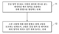
도 1에 예시된 바와 같이, 본 개시내용의 상판을 형성하는 방법은 다음의 단계를 포함할 수 있다: 11) 중심 영역 및 테이퍼진 에지 영역을 포함하는 상판 블랭크를 형성하는 단계로서, 상판 블랭크의 길이방향에 대한 테이퍼진 에지 영역의 테이퍼 각도는 20도 이하인 단계, 및 12) 상판 블랭크의 외부 표면 상에 코팅을 도포하는 단계로서, 코팅은 중심 영역 전체 및 테이퍼진 에지 영역의 적어도 일부 위에 놓이는, 단계.As illustrated in FIG. 1 , a method of forming a top plate of the present disclosure may include the following steps: 11) forming a top plate blank including a center region and a tapered edge region, wherein the a taper angle of the tapered edge region with respect to the longitudinal direction is 20 degrees or less, and 12) applying a coating on the outer surface of the top blank, wherein the coating overlies the entire central region and at least a portion of the tapered edge region; step.
상판 블랭크의 형성 단계(11)는 표준 상업용 웨이퍼, 예를 들어 원형 웨이퍼 잉곳으로부터 절단된 얇은 슬라이스를 사용하고, 웨이퍼 재료를 제거하도록 웨이퍼를 제어된 절단 및/또는 연마를 받게 하여 웨이퍼의 에지 영역에 평활한 감소 테이퍼를 형성함으로써 수행될 수 있다. 특정 실시예에서, 테이퍼는 제어된 연마에 의해 형성될 수 있다. 다른 양태에서, 웨이퍼의 테이퍼는 제어된 에칭에 의해 제조될 수 있다.
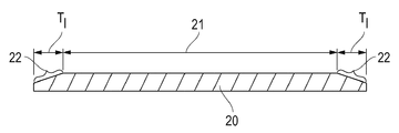
도 2a는 상판 블랭크의 중심 영역(21) 및 테이퍼진 에지 영역(22)을 보여주는, 본 개시내용의 실시예에 따른 상판 블랭크(20)의 측면도의 예시를 포함한다.2A includes an illustration of a side view of a top blank 20 according to an embodiment of the present disclosure, showing a
도 2b는 도 2a에 도시된 상판의 확대된 섹션을 예시하는 것으로, 전체 테이퍼진 에지 영역(22) 및 중심 영역(21)의 일부를 보여준다. 중심 영역(21)으로부터 테이퍼진 에지 영역(22)으로의 평활한 천이를 볼 수 있다. 테이퍼진 에지 영역(22) 전체에 걸친 테이퍼의 평균 테이퍼 각도(23)는 20도 이하일 수 있다. 특정 양태에서, 도 2b에 예시된 바와 같이, 테이퍼 각도는 테이퍼진 에지 영역 전체에 걸쳐 동일할 수 있다. 다른 특정 양태(도시되지 않음)에서, 테이퍼 각도는 테이퍼진 에지 영역 내에서 달라질 수 있으며, 예를 들어 테이퍼 각도는 외부 에지를 향해 증가할 수 있다. 양태에서, 테이퍼진 에지 영역 전체에 걸친 평균 테이퍼 각도는 18도 이하, 예를 들어 15도 이하, 10도 이하, 8도 이하, 7도 이하, 6도 이하, 5도 이하, 또는 3도 이하일 수 있다.FIG. 2B illustrates an enlarged section of the top plate shown in FIG. 2A , showing the entire tapered
특정 양태에서, 중심 영역(21) 및 테이퍼진 에지 영역(22)을 포함하는 상판 블랭크의 직경은 적어도 50 mm, 예를 들어 적어도 100 mm, 적어도 150 mm, 적어도 200 mm, 적어도 250 mm, 적어도 280 mm, 또는 적어도 290 mm일 수 있다. 다른 양태에서, 중심 영역의 직경은 600 nm 이하, 예를 들어 500 mm 이하, 450 mm 이하, 또는 400 mm 이하일 수 있다. 상판 블랭크의 직경은 위에서 언급한 임의의 최소값과 최대값 사이의 값일 수 있다.In certain aspects, the diameter of the top blank comprising the
일 양태에서, 상판 블랭크의 표면적 비율 Sc:St(Sc는 중심 영역(21)의 표면적이고, St는 테이퍼진 에지 영역(21)의 표면적임)는 적어도 15, 예를 들어 적어도 20, 적어도 30, 적어도 40, 적어도 45, 또는 적어도 50일 수 있다.In one aspect, the surface area ratio Sc:St (Sc is the surface area of the
또 다른 양태에서, 중심 영역(21)에서 상판 블랭크의 두께(Sd)는 적어도 100 미크론, 예를 들어 적어도 150 미크론, 적어도 200 미크론, 적어도 300 미크론, 적어도 500 미크론, 적어도 1000 미크론, 또는 적어도 2000 미크론일 수 있다. 다른 양태에서, 두께는 5000 미크론 이하, 4000 미크론 이하, 또는 3000 미크론 이하일 수 있다. 중심 영역에서 상판 블랭크의 두께는 위에서 언급한 임의의 최소값과 최대값 사이의 값일 수 있다. In another aspect, the thickness S d of the top blank in the
본 개시내용의 상판 블랭크의 테이퍼진 에지 영역(22)은 적어도 1.0 mm, 예를 들어 적어도 1.5 mm, 적어도 1.8 mm, 적어도 2.0 mm, 적어도 2.3 mm, 적어도 2.5 mm, 또는 적어도 3.0 mm의 반경방향(x-축)으로의 길이(Tl)를 가질 수 있다. 다른 양태에서, 테이퍼진 에지 영역(Tl)은 5.0 mm 이하, 예를 들어 4.5 mm 이하, 4.0 mm 이하, 또는 3.5 mm 이하일 수 있다. 테이퍼진 에지 영역의 Tl는 위에서 언급한 임의의 최소 수 및 최대 수 사이의 값일 수 있다는 것이 이해될 것이다.The tapered
추가 양태에서, 상판 블랭크의 높이 방향(y-축)으로 상판 블랭크의 중심 영역의 외부 표면의 레벨로부터 상판 블랭크의 외부 에지에서 테이퍼의 깊이(Td)는 적어도 20 미크론, 예를 들어 적어도 30 미크론, 또는 적어도 50 미크론, 또는 적어도 80 미크론, 또는 적어도 100 미크론일 수 있다. 다른 양태에서, 테이퍼 깊이(Td)는 400 미크론 이하, 예를 들어 350 미크론 이하, 300 미크론 이하, 250 미크론 이하, 200 미크론 이하, 또는 150 미크론 이하일 수 있다. 테이퍼의 깊이(Td)는 위에서 언급한 임의의 최소값과 최대값 사이의 값일 수 있다. 특정 예에서, Td는 중심 영역에서 상판 블랭크의 두께와 동일할 수 있다. 예를 들어, 상판 블랭크의 두께가 중심 영역에서 100 미크론인 경우, Td도 100 미크론일 수 있다. In a further aspect, the depth (T d ) of the taper at the outer edge of the top blank from the level of the outer surface of the central region of the top blank in the height direction (y-axis) of the top blank is at least 20 microns, for example at least 30 microns. , or at least 50 microns, or at least 80 microns, or at least 100 microns. In other aspects, the taper depth T d can be 400 microns or less, such as 350 microns or less, 300 microns or less, 250 microns or less, 200 microns or less, or 150 microns or less. The depth of the taper (T d ) may be any value between the minimum and maximum values mentioned above. In certain instances, T d may be equal to the thickness of the top blank in the central region. For example, when the thickness of the top blank is 100 microns in the central region, T d may also be 100 microns.
상판 블랭크는 다양한 재료로 제조될 수 있다. 재료의 비제한적인 예는 유리 기반 재료, 실리콘, 스피넬, 융합 실리카, 석영, 유기 폴리머, 실록산 폴리머, 플루오로카본 폴리머, 금속, 금속 합금, 경화된 사파이어, 퇴적된 산화물, 양극 산화된 알루미나, 유기 실란, 유기 실리케이트 재료, 무기 폴리머, 또는 이들의 임의의 조합을 포함할 수 있다. 유리 기반 재료는 소다 석회 유리, 붕규산염 유리, 알칼리-바륨 실리케이트 유리, 석영 유리, 알루미노실리케이트 유리, 또는 합성 융합 실리카를 포함할 수 있다.The top blank may be made of various materials. Non-limiting examples of materials include glass based materials, silicon, spinel, fused silica, quartz, organic polymers, siloxane polymers, fluorocarbon polymers, metals, metal alloys, hardened sapphires, deposited oxides, anodized alumina, organic silanes, organosilicate materials, inorganic polymers, or any combination thereof. The glass-based material may include soda-lime glass, borosilicate glass, alkali-barium silicate glass, quartz glass, aluminosilicate glass, or synthetic fused silica.
본 개시내용의 방법의 일 실시예에서, 상판 블랭크(12) 상에 코팅을 도포하는 것은 스핀 코팅에 의해 수행될 수 있다. 전술한 구조의 테이퍼진 상판 블랭크를 사용함으로써, 상판 블랭크 상에 보호 코팅이 형성될 수 있으며, 코팅의 에지 비드는 테이퍼의 경사를 따라 아래로 이동될 수 있다.In one embodiment of the method of the present disclosure, applying the coating on the top blank 12 may be performed by spin coating. By using the tapered top blank of the above structure, a protective coating can be formed on the top blank, and the edge bead of the coating can be moved down along the inclination of the taper.
본 개시내용의 특정 양태에서, 에지 비드의 형성은 심지어는 완전히 방지될 수 있다. 이는 본 발명의 테이퍼진 에지 영역을 포함하지 않는 상판 블랭크 상에서 스핀 코팅을 수행하면 달성될 수 없다.In certain aspects of the present disclosure, the formation of edge beads can even be completely prevented. This cannot be achieved by performing spin coating on the top blank that does not include the tapered edge region of the present invention.
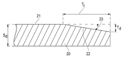
도 3a는 상판의 실시예를 예시하고 코팅(24)은 스핀 코팅을 통해 상판 블랭크(20) 상에 도포된다. 도 3a는 테이퍼진 에지 영역(22) 전체 및 중심 영역(21)의 일부를 갖는 상판의 섹션 만을 도시한다. 코팅(24)이 상판 블랭크의 중심 영역(21) 위에 균일하게 놓일 수 있고 테이퍼진 에지 영역(22) 내에 에지 비드(25)를 형성할 수 있음을 알 수 있다. 일 양태에서, 에지 비드(25)의 정점(26)은 중심 영역(21) 내의 코팅(24)의 외부 표면의 평면(27) 아래에 있을 수 있다.Figure 3a illustrates an embodiment of the top plate and the
일 실시예에서, 코팅(24)은 폴리머 코팅일 수 있다. 폴리머 코팅 재료의 비제한적인 예는 폴리(메틸 메타크릴레이트)(poly(methyl methacrylate))(PMMA), 플루오로폴리머, 또는 폴리에틸렌 테레프탈레이트 또는 평탄화 프로세스 동안 형성 가능한 재료를 경화하는 데 사용되는 선택된 화학 방사선, 예를 들어, 특정 UV 광파 범위에 투명한 임의의 폴리머일 수 있다.In one embodiment, the
다른 실시예에서, 코팅(24)은 중심 영역 내에서 적어도 0.1 미크론, 예를 들어 적어도 0.5 미크론, 적어도 1.0 미크론, 적어도 2.0 미크론, 적어도 3 미크론, 또는 적어도 5 미크론의 평균 두께를 가질 수 있다. 또 다른 양태에서, 중심 영역 내의 코팅은 10 미크론 이하, 예를 들어 8 미크론 이하, 또는 6 미크론 이하일 수 있다. 중심 영역 내의 코팅 두께는 위에서 언급한 임의의 최소값과 최대값 사이의 값일 수 있다.In other embodiments, the
특정 실시예에서, 코팅(24)은 단일층 코팅일 수 있다. 다른 특정 실시예에서, 코팅은 다층 코팅일 수 있다.In certain embodiments, the
코팅(24)은 중심 영역 전체에 걸쳐 높은 평탄도와 평활도를 가질 수 있다. 일 양태에서, 중심 영역 내의 코팅의 표면 거칠기는 5 nm 이하, 예를 들어 3 nm 이하, 2 nm 이하, 1.5 nm 이하, 또는 1 nm 이하일 수 있다.The
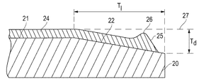
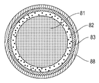
본 개시내용의 상판의 추가 이점은 테이퍼진 에지 영역이 상판의 분리 구역의 일부일 수 있다는 점일 수 있다. 분리 구역은 기판으로부터 상판을 분리하는 것을 돕기 위해 평탄화 단계 후에 상판과 기판 사이의 진공을 파괴하는 기능을 갖는 리세스 또는 간극을 포함할 수 있는 상판의 외부 에지에 있는 영역이다. 분리 구역은 통상적으로 약 2-3 mm의 반경방향 길이를 가지며 기판의 평탄화를 위한 접촉 표면적으로서 참여하지 않는다. 도 4a에 예시된 바와 같이, 테이퍼진 에지 영역(73) 및 분리 구역(78)이 동일한 웨이퍼 영역을 덮도록 분리 구역을 테이퍼진 에지 영역으로 수정함으로써, 형성된 에지 비드를 분리 구역의 영역으로 전달하고 기판 평탄화에 적절한 큰 표면적(71)을 획득하는 것이 가능하다. 비교하면, 스핀 코팅된 보호 코팅이 있는 통상적인 상판은 도 4b에 예시된 바와 같이 분리 구역(88) 및 분리 구역(88) 옆에 에지 비드 구역(83)을 포함한다. 더욱이, 본 명세서에서 "에지-이웃 구역"(82)이라고 명명되는 에지 비드 구역(83) 옆의 영역을 고려해야 하며, 훨씬 더 높은 결함 가능성이 에지 비드를 제거하는 노력에 의해 야기되는 것으로 예상될 수 있고 또한 기판을 평탄화하기 위한 적절한 표면적(81)으로부터 차감될 수 있다. 따라서, 본 발명의 상판은, 큰 표면적(71)이 기판을 평탄화하는 데 사용될 수 있고, 에지 비드의 제거가 필요없을 수 있다는 이점이 있다. 더욱이, 이를 통해 추가 프로세스 단계를 피할 수 있고 에지 비드를 제거하는 동안 상판에 손상을 일으킬 위험을 감소시킬 수 있다.A further advantage of the top plate of the present disclosure may be that the tapered edge region may be part of a separation zone of the top plate. A separation zone is an area at the outer edge of the top plate that may include a recess or gap that functions to break the vacuum between the top plate and the substrate after the planarization step to aid in separating the top plate from the substrate. The separation zone typically has a radial length of about 2-3 mm and does not participate as a contact surface area for planarization of the substrate. 4A, by modifying the separation zone to a tapered edge region so that the tapered edge region 73 and the separation region 78 cover the same wafer region, transferring the formed edge bead to the region of the separation region and It is possible to obtain a
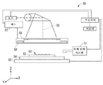
도 5를 참조하면, 본 명세서에 설명된 실시예에 따른 장치(50)는 본 개시내용의 상판(58)을 사용하여 기판(52)을 평탄화하는 데 사용될 수 있다. 상판(58)은 기판(52)으로부터 이격되어 위치 설정될 수 있다.Referring to FIG. 5 , an
기판(52)은 실리콘 웨이퍼와 같은 반도체 모재일 수 있지만, 유리, 사파이어, 스피넬 등과 같은 절연성 모재를 포함할 수 있다. 기판(52)은 기판 홀더(54), 예를 들어 척에 결합될 수 있다. 척은 진공, 핀형, 홈형, 정전기, 전자기 등을 포함하는 임의의 척일 수 있다. 기판(52) 및 기판 홀더(54)는 스테이지(56)에 의해 추가로 지지될 수 있다. 스테이지(56)는 X, Y, 또는 Z 방향을 따라 병진 또는 회전 운동을 제공할 수 있다.The
상판(58)은 기판(52) 상에 퇴적된 형성 가능한 재료를 평탄화하는 데 사용될 수 있다. 상판(58)은 상판 홀더(59)에 결합될 수 있다. 상판(58)은 상판 홀더(59)에 의해 유지되고 그 형상이 조절될 수 있다. 상판 홀더(59)는 척킹 영역 내에 상판(58)을 유지하도록 구성될 수 있다. 상판 홀더(59)는 진공, 핀형, 홈형, 정전기, 전자기, 또는 다른 유사한 홀더 유형으로 구성될 수 있다. 일 실시예에서, 상판 홀더(59)는 상판 홀더(59)의 본체 내에 투명 윈도우를 포함할 수 있다.The
장치(50)는 기판(52)의 표면 상에 형성 가능한 재료(53)를 퇴적하기 위한 유체 분배 시스템(51)을 더 포함할 수 있다. 형성 가능한 재료(53)는, 액적 분배, 스핀 코팅, 딥 코팅, 화학 기상 증착(chemical vapor deposition)(CVD), 물리 기상 증착(physical vapor deposition)(PVD), 박막 퇴적, 후막 퇴적, 또는 이들의 조합과 같은 기술을 사용하여 하나 이상의 층으로 기판(52) 상에 위치 설정될 수 있다. 형성 가능한 재료(53)는 원하는 체적이 상판(58)과 기판(52) 사이에 형성되기 전 또는 후에 기판(52) 상에 분배될 수 있다. 형성 가능한 재료(53)는 화학 방사선 및/또는 열을 사용하여 경화될 수 있는 하나 이상의 중합 가능한 모노머 및/또는 올리고머 및/또는 폴리머를 포함할 수 있다.The
본 개시내용은 또한 물품을 제조하는 방법에 관한 것이다. 이 방법은, 기판 상에 형성 가능한 재료의 층을 도포하는 단계; 형성 가능한 재료의 층을 본 개시내용의 상판과 접촉시키는 단계; 및 형성 가능한 재료를 광 또는 열로 경화시켜 경화된 층을 형성하는 단계를 포함할 수 있다. 기판 및 경화된 층은, 예를 들어, 고체화된 층 및/또는 고체화된 층 아래에 있는 패턴화된 층 중 하나 또는 둘 모두의 패턴에 대응하는 이미지를 기판으로 전사하는 에칭 프로세스를 포함함으로써, 원하는 물품을 형성하도록 추가 처리를 받을 수 있다. 기판은, 예를 들어 경화, 산화, 층 형성, 퇴적, 도핑, 평탄화, 에칭, 형성 가능한 재료 제거, 다이싱, 접합, 및 패키징 등을 비롯하여 디바이스(물품) 제조를 위한 공지된 단계 및 프로세스를 추가로 받을 수 있다. 특정 양태에서, 기판은 복수의 물품을 생성하도록 처리될 수 있다.The present disclosure also relates to a method of making the article. The method includes applying a layer of a formable material onto a substrate; contacting the layer of formable material with a top plate of the present disclosure; and curing the formable material with light or heat to form a cured layer. The substrate and the cured layer may be prepared by including, for example, an etching process that transfers to the substrate an image corresponding to the pattern of one or both of the solidified layer and/or the patterned layer underlying the solidified layer, thereby It may be subjected to further processing to form the article. The substrate adds known steps and processes for device (article) fabrication, including, for example, curing, oxidation, layering, deposition, doping, planarization, etching, formable material removal, dicing, bonding, packaging, and the like. can be received with In certain aspects, the substrate may be processed to produce a plurality of articles.
경화된 층은 LSI, 시스템 LSI, DRAM, SDRAM, RDRAM 또는 D-RDRAM과 같은 반도체 디바이스의 개재층 절연막으로서, 또는 반도체 제조 프로세스에서 사용되는 레지스트 막으로서 추가로 사용될 수 있다.The cured layer may further be used as an interlayer insulating film of a semiconductor device such as LSI, system LSI, DRAM, SDRAM, RDRAM or D-RDRAM, or as a resist film used in a semiconductor manufacturing process.
예에서 추가로 입증된 바와 같이, 에지 비드의 정점이 중심 영역의 코팅 레벨보다 아래에 있을 수 있음을 야기할 수 있는 특정 테이퍼진 에지 설계를 상판 블랭크가 포함하는 경우, 상판 블랭크 상의 보호 코팅의 스핀 코팅 동안 형성된 원치않는 에지 비드가 용인될 수 있다는 것을 발견하였다.As further demonstrated in the example, the spin of the protective coating on the top blank when the top blank includes a specific tapered edge design that can cause the apex of the edge bead to be below the coating level in the central region. It has been found that unwanted edge beads formed during coating can be tolerated.
예Yes
다음의 비제한적인 예는 본 명세서에 설명된 개념을 예시한다.The following non-limiting examples illustrate the concepts described herein.
예 1Example 1
300 mm의 직경 및 700 미크론의 두께를 갖는 원형 융합 실리카 웨이퍼를 웨이퍼의 에지 영역에서 제어된 절단을 받게 하여 테이퍼를 형성함으로써 상판 블랭크를 제조하였다. 절단은 연마에 의해 수행되었다.A top blank was prepared by subjecting a circular fused silica wafer having a diameter of 300 mm and a thickness of 700 microns to a controlled cut in the edge region of the wafer to form a taper. Cutting was performed by grinding.
획득된 상판 블랭크는 다음의 에지 프로파일을 갖는다: 1,8667 mm의 테이퍼진 에칭 영역의 길이(Tl); 226 미크론의 웨이퍼의 외부 에지에서의 테이퍼 깊이(Td); 및 6.8°의 테이퍼 각도.The obtained top blank had the following edge profile: length of the tapered etched area (T 1 ) of 18667 mm; a taper depth (T d ) at the outer edge of the wafer of 226 microns; and a taper angle of 6.8°.
MicroChem사의 액체 코팅 조성물 495 PMMA 8 ml을 스핀 코팅을 통해 도포하고 약 180℃의 온도에서 경화시킴으로써 상판 블랭크의 상부 외부 표면 상에 폴리(메틸 메타크릴레이트)(PMMA) 코팅을 형성하였다. 액체 코팅 조성물은 23℃에서 204 cP의 점도를 가지며 Tel Act12 스핀 코팅기를 사용하여 20 초 동안 1000 rpm의 회전 속도로 도포하였고, 1750 rpm에서 55 초 동안 건조시켰다. 상판 블랭크의 중심 영역에서 PMMA 코팅의 두께는 약 2 미크론이었다.A poly(methyl methacrylate) (PMMA) coating was formed on the upper outer surface of the top blank by applying 8 ml of MicroChem's liquid coating composition 495 PMMA via spin coating and curing at a temperature of about 180°C. The liquid coating composition had a viscosity of 204 cP at 23° C. and was applied using a Tel Act12 spin coater at a rotation speed of 1000 rpm for 20 seconds and dried at 1750 rpm for 55 seconds. The thickness of the PMMA coating in the central region of the top blank was about 2 microns.
코팅의 형성된 에지 비드의 위치 및 크기는 Bruker Insight 원자간력 프로파일링(Atomic Force Profiling)(AFP)을 사용하여 분석되었다. 도 6에 예시된 바와 같이, 에지 비드는 상판 블랭크의 외부 에지에 매우 가깝게 테이퍼진 에지 영역 내에 형성된다. 에지 비드는 상판의 중심 지점으로부터 약 148.15 mm 반경방향 거리에 그 정점(66)을 가지며, 이는 상판의 외부 에지로부터 1.785 mm에 대응한다.The location and size of the formed edge beads of the coating were analyzed using Bruker Insight Atomic Force Profiling (AFP). As illustrated in FIG. 6 , the edge bead is formed in an edge region that tapers very close to the outer edge of the top blank. The edge bead has its apex 66 at a radial distance of about 148.15 mm from the center point of the top plate, which corresponds to 1.785 mm from the outer edge of the top plate.
에지 비드의 정점(66)이 상판 블랭크의 중심 영역에 있는 코팅의 평면보다 낮다는 것을 도 6에서 또한 명확하게 알 수 있다. 도 6에서, 중심 영역(67)에서 상판 블랭크의 외부 표면 아래에 정점의 거리는 -0.35 미크론이었다. 중심 영역에서 약 2 미크론의 코팅 두께의 두께를 추가하면, 에지 비드의 정점은 -2.35 미크론의 음의 높이(He)를 가졌다. 데이터 요약은 아래의 표 1에 또한 나타낸다.It can also be clearly seen in FIG. 6 that the apex 66 of the edge bead is lower than the plane of the coating in the central region of the top blank. 6 , the distance of the apex below the outer surface of the top blank in the central region 67 was −0.35 microns. Adding the thickness of the coating thickness of about 2 microns in the central region, the apex of the edge bead had a negative height (He) of -2.35 microns. A data summary is also presented in Table 1 below.
비교예 2Comparative Example 2
습식 에칭된 측면 영역을 갖는 상판 블랭크의 스핀 코팅.Spin coating of a top blank with wet etched side areas.
에지 영역에서 상판 블랭크의 습식 에칭은 통상적으로 분리 구역을 갖는 스핀 코팅된 상판을 제조하기 위해 수행된다.Wet etching of the top blank in the edge region is typically performed to produce a spin coated top plate with separation zones.
출발 재료(에칭 전)로서 예 1과 동일한 웨이퍼(테이퍼진 에지를 도입하기 전)를 사용하였다. 습식 에칭은 웨이퍼의 중심을 향해 반경방향으로 웨이퍼의 외부 에지로부터 약 3 mm의 영역에 걸쳐 수행되었다. 웨이퍼를 에칭하여, 웨이퍼의 전체 3 mm 외부 원 영역에 걸쳐 웨이퍼의 두께 방향(y)(깊이(Td)로도 표시됨)으로 50 미크론의 웨이퍼 재료를 제거하였다.The same wafer as in Example 1 (before introducing tapered edges) was used as the starting material (before etching). The wet etch was performed over an area of about 3 mm from the outer edge of the wafer in a radial direction towards the center of the wafer. The wafer was etched to remove 50 microns of wafer material in the thickness direction y (also denoted depth T d ) of the wafer over the entire 3 mm outer circle area of the wafer.
예 1에도 사용된 바와 같은 MicroChem사의 액체 코팅 조성물 495 PMMA를 도포함으로써 상판 블랭크의 상부 외부 표면 상에 a) 약 2 미크론 및 b) 약 1 미크론의 두께를 갖는 폴리(메틸 메타크릴레이트)(PMMA) 코팅을 형성하도록 스핀 코팅 실험을 수행하였다.Poly(methyl methacrylate) (PMMA) having a thickness of a) about 2 microns and b) about 1 micron on the upper outer surface of the top blank by applying a liquid coating composition 495 PMMA from MicroChem as also used in Example 1 Spin coating experiments were performed to form a coating.
형성된 층의 에지 비드는 Zygo NewView 3D 광학 표면 프로파일 분석기를 사용하여 분석되었다.The edge beads of the formed layer were analyzed using a Zygo NewView 3D optical surface profile analyzer.
스핀 코팅 동안 형성된 에지 비드의 분석은, 습식 에칭에 의해 웨이퍼 높이의 감소가 야기되기 전에 에지 비드의 위치가 짧다는 것을 보여주었다.Analysis of the edge bead formed during spin coating showed that the position of the edge bead was short before wet etching caused a reduction in wafer height.
표 1은, 웨이퍼 중심 영역의 코팅의 외부 표면의 평면으로부터 에지 비드의 정점까지의 수직 방향 거리로 표현된, 형성된 에지 비드의 높이(He); 및 코팅의 외부 표면의 레벨에서 에지 비드의 폭을 나타내는, 에지 비드의 폭(We)과 같은 측정 데이터의 요약을 포함한다.Table 1 shows the height (He) of the formed edge bead, expressed as the vertical distance from the plane of the outer surface of the coating in the wafer center region to the apex of the edge bead; and a summary of measurement data, such as the width of the edge bead (We), representing the width of the edge bead at the level of the outer surface of the coating.
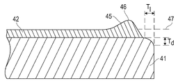
비교예 2의 상판의 선도는 도 3b에 예시되어 있다. 에칭은 상판 블랭크(31)의 높이를 갑작스럽게 감소시켰으며, 감소의 평균 테이퍼 각도(33)는 45도 이상임을 알 수 있다. 스핀 코팅에 의해 도포된 코팅(32)은 웨이퍼의 에칭된 부분의 갑작스런 표면 강하 전에 정점(36)의 위치가 가까운 에지 비드(35)를 형성하였다. 에지 비드(35)의 정점(36)은 중심 영역 내에서 코팅(32)의 외부 표면 레벨(37)의 위에 있다.A diagram of the upper plate of Comparative Example 2 is illustrated in FIG. 3B . It can be seen that the etching abruptly reduced the height of the top blank 31, and the
비교예 3Comparative Example 3
본 발명에 따른 테이퍼진 에지 영역을 갖지 않는 상판 블랭크 상에서 에지 비드 형성을 시뮬레이션하기 위해, 에지 영역의 추가 수정 없이 예 1의 상업용 융합 실리카 웨이퍼를 사용하였다. 웨이퍼는 웨이퍼의 매우 짧은 반경방향 거리에 걸쳐 표준 원형 에지를 포함하였다.To simulate edge bead formation on a top blank having no tapered edge region according to the present invention, the commercial fused silica wafer of Example 1 was used without further modification of the edge region. The wafer contained a standard circular edge over a very short radial distance of the wafer.
웨이퍼는 다음과 같은 에지 프로파일을 갖는다: 50-85 미크론의 에지 영역의 길이(Tl); 25-48 미크론의 웨이퍼의 외부 에지에서의 깊이(Td), 및 약 45도 이상의 웨이퍼의 반경방향 x에 관한 원형 에지를 따른 각도.The wafer has the following edge profiles: length of the edge region (T 1 ) of 50-85 microns; A depth (T d ) at the outer edge of the wafer of 25-48 microns, and an angle along the circular edge about the radial x of the wafer of about 45 degrees or greater.
웨이퍼는 비교예 2에서 수행된 바와 동일한 PMMA 코팅 및 중심 영역에서의 코팅 두께(약 1 미크론 및 약 2 미크론)로 스핀 코팅되었다.The wafers were spin coated with the same PMMA coating as done in Comparative Example 2 and coating thicknesses in the central region (about 1 micron and about 2 microns).
웨이퍼 분석은, 스핀 코팅이 웨이퍼의 외부 영역에서 외부 에지에 약 2 mm 가까운 에지 비드를 형성했음을 보여주었다.Wafer analysis showed that the spin coating formed an edge bead in the outer region of the wafer, approximately 2 mm close to the outer edge.
웨이퍼(41) 및 도포된 코팅(42)의 선도가 도 3c에 예시되어 있다. 원형 에지 영역 이전에 에지 비드(45)가 형성된 것을 볼 수 있으며, 에지 비드(45)의 정점(46)은 중심 영역 내의 코팅의 외부 표면의 평면(47)보다 훨씬 더 높았다.A diagram of the
데이터의 비교:Comparison of data:
표 1은 형성된 에지 비드의 높이(He), 및 에지 비드의 폭(We)과 같은 예 1, 비교예 2 및 3의 측정 데이터의 요약을 포함한다. 높이(He)와 폭(We) 모두는 중심 영역의 코팅의 외부 표면 레벨을 시작 위치로 사용하여 측정되었다.Table 1 contains a summary of the measurement data of Example 1, Comparative Examples 2 and 3, such as the height (He) of the formed edge bead, and the width (We) of the edge bead. Both the height (He) and width (We) were measured using the outer surface level of the coating in the central region as the starting position.

표 1에 요약된 테스트 데이터는, 웨이퍼의 에지 영역에서 약 2 mm의 영역에 걸쳐 평활하게 감소하는 테이퍼를 갖는 예 1의 상판만이 중심 영역 내의 코팅 레벨 아래의 정점을 갖는 에지 비드를 포함한다는 것을 보여준다.The test data summarized in Table 1 show that only the top plate of Example 1, which had a smooth decreasing taper over an area of about 2 mm in the edge region of the wafer, contained an edge bead with an apex below the coating level in the central region. show
웨이퍼의 3 mm 외부 링 영역에서 에칭을 받고 스핀 코팅된 웨이퍼는, 중심 영역의 코팅 평면 위의 정점 높이를 갖는 에지 비드를 포함하였다. 그러나, 스핀 코팅된 표준 웨이퍼의 에지 비드와 비교하여, 습식 에칭된 웨이퍼는 정점의 높이가 훨씬 낮았다. 비교예 C2 및 C3의 웨이퍼를 상판으로 사용하기 위해서는, 예를 들어 용해 또는 연마를 통해 에지 비드를 제거할 필요가 있는 반면, 예 1의 상판에 포함된 에지 비드는 용인될 수 있다. 그러나, 특정 예에서, 본 개시내용의 상판의 에지 비드도, 예를 들어 용매로 세정함으로써 제거될 수 있다.The etched and spin coated wafer in the 3 mm outer ring region of the wafer contained edge beads with an apex height above the coating plane in the central region. However, compared to the edge bead of the spin-coated standard wafer, the wet-etched wafer had a much lower apex height. In order to use the wafers of Comparative Examples C2 and C3 as the top plate, it is necessary to remove the edge bead through, for example, melting or polishing, whereas the edge bead included in the top plate of Example 1 may be tolerated. However, in certain instances, the edge beads of the top plate of the present disclosure may also be removed, for example, by washing with a solvent.
Claims (14)
상기 상판 블랭크는 중심 영역 및 테이퍼진 에지 영역을 포함하고;
상기 테이퍼진 에지 영역은 상기 상판 블랭크의 반경방향에 대해 20도 이하의 평균 테이퍼 각도를 가지며;
상기 코팅은 상기 상판 블랭크의 상기 중심 영역 및 상기 테이퍼진 에지 영역의 적어도 일부 위에 놓이는, 상판.A top plate comprising a top blank and a coating overlying an outer surface of the top blank, the top plate comprising:
the top blank includes a central region and a tapered edge region;
the tapered edge region has an average taper angle of 20 degrees or less with respect to the radial direction of the top blank;
and the coating overlies at least a portion of the central region and the tapered edge region of the top blank.
중심 영역 및 테이퍼진 에지 영역을 포함하는 상판 블랭크를 준비하는 단계로서, 상기 상판 블랭크의 반경방향에 대한 상기 테이퍼진 에지 영역의 테이퍼 각도는 20도 이하인, 단계; 및
상기 상판 블랭크의 외부 표면 상에 코팅을 도포하는 단계로서, 상기 코팅은 상기 중심 영역 전체 및 상기 테이퍼진 에지 영역의 적어도 일부 위에 놓이는, 단계를
포함하는, 방법.A method of forming a top plate, comprising:
preparing a top plate blank including a center region and a tapered edge region, wherein a taper angle of the tapered edge region with respect to a radial direction of the top blank is 20 degrees or less; and
applying a coating on the outer surface of the top blank, the coating overlying all of the central region and at least a portion of the tapered edge region;
Including method.
기판 상에 경화 가능한 조성물의 층을 도포하는 단계;
상기 경화 가능한 조성물을 상판과 접촉시키는 단계로서, 상기 상판은 상판 블랭크 및 상기 상판 블랭크의 외부 표면 위에 놓인 코팅을 포함하고,
상기 상판 블랭크는 중심 영역 및 테이퍼진 에지 영역을 포함하고;
상기 테이퍼진 에지 영역은 상기 상판 블랭크의 길이방향에 대해 20도 이하의 테이퍼 각도를 가지며;
상기 코팅은 상기 상판 블랭크의 상기 중심 영역 전체 및 상기 테이퍼진 에지 영역의 적어도 일부 위에 놓이는, 단계;
상기 경화 가능한 조성물을 광 또는 열로 경화시켜 경화된 층을 형성하는 단계;
상기 경화된 층으로부터 상기 상판을 제거하는 단계; 및
상기 경화된 층으로 상기 기판을 처리하여 상기 물품을 제조하는 단계를 포함하는, 방법.A method of making an article, comprising:
applying a layer of a curable composition onto a substrate;
contacting the curable composition with a top plate, the top plate comprising a top blank and a coating overlying an outer surface of the top blank;
the top blank includes a central region and a tapered edge region;
the tapered edge region has a taper angle of 20 degrees or less with respect to the longitudinal direction of the top blank;
the coating overlying all of the central region and at least a portion of the tapered edge region of the top blank;
curing the curable composition with light or heat to form a cured layer;
removing the top plate from the cured layer; and
processing the substrate with the cured layer to make the article.
Applications Claiming Priority (2)
| Application Number | Priority Date | Filing Date | Title |
|---|---|---|---|
| US16/834,465 US20210305082A1 (en) | 2020-03-30 | 2020-03-30 | Superstrate and method of making it |
| US16/834,465 | 2020-03-30 |
Publications (1)
| Publication Number | Publication Date |
|---|---|
| KR20210122100A true KR20210122100A (en) | 2021-10-08 |
Family
ID=77854686
Family Applications (1)
| Application Number | Title | Priority Date | Filing Date |
|---|---|---|---|
| KR1020210034972A KR20210122100A (en) | 2020-03-30 | 2021-03-18 | Superstrate and method of making it |
Country Status (4)
| Country | Link |
|---|---|
| US (1) | US20210305082A1 (en) |
| JP (1) | JP2021160352A (en) |
| KR (1) | KR20210122100A (en) |
| CN (1) | CN113471101A (en) |
Families Citing this family (2)
| Publication number | Priority date | Publication date | Assignee | Title |
|---|---|---|---|---|
| US11562924B2 (en) * | 2020-01-31 | 2023-01-24 | Canon Kabushiki Kaisha | Planarization apparatus, planarization process, and method of manufacturing an article |
| US11878935B1 (en) * | 2022-12-27 | 2024-01-23 | Canon Kabushiki Kaisha | Method of coating a superstrate |
Family Cites Families (5)
| Publication number | Priority date | Publication date | Assignee | Title |
|---|---|---|---|---|
| US20080160129A1 (en) * | 2006-05-11 | 2008-07-03 | Molecular Imprints, Inc. | Template Having a Varying Thickness to Facilitate Expelling a Gas Positioned Between a Substrate and the Template |
| JP6385131B2 (en) * | 2014-05-13 | 2018-09-05 | 株式会社ディスコ | Wafer processing method |
| JP2017010962A (en) * | 2015-06-16 | 2017-01-12 | 株式会社東芝 | Device substrate and method of manufacturing device substrate, and method of manufacturing semiconductor device |
| US11137536B2 (en) * | 2018-07-26 | 2021-10-05 | Facebook Technologies, Llc | Bragg-like gratings on high refractive index material |
| KR20210026955A (en) * | 2019-09-02 | 2021-03-10 | 삼성전자주식회사 | Semiconductor device manufacturing equipment, semiconductor device inspection device, and semiconductor device manufacturing method |
-
2020
- 2020-03-30 US US16/834,465 patent/US20210305082A1/en active Pending
-
2021
- 2021-01-13 JP JP2021003721A patent/JP2021160352A/en active Pending
- 2021-03-18 KR KR1020210034972A patent/KR20210122100A/en active Search and Examination
- 2021-03-30 CN CN202110337576.7A patent/CN113471101A/en active Pending
Also Published As
| Publication number | Publication date |
|---|---|
| US20210305082A1 (en) | 2021-09-30 |
| TW202136013A (en) | 2021-10-01 |
| CN113471101A (en) | 2021-10-01 |
| JP2021160352A (en) | 2021-10-11 |
Similar Documents
| Publication | Publication Date | Title |
|---|---|---|
| KR20210122100A (en) | Superstrate and method of making it | |
| KR102401043B1 (en) | Extreme ultraviolet lithography mask blank manufacturing system and method of operation therefor | |
| US8048775B2 (en) | Process of forming ultra thin wafers having an edge support ring | |
| JP6688221B2 (en) | Glass-ceramics for ultraviolet lithography and method for producing the same | |
| US10192741B2 (en) | Device substrate, method of manufacturing device substrate, and method of manufacturing semiconductor device | |
| TWI430362B (en) | Method for routing a chamfered substrate | |
| EP2339399B1 (en) | Photomask-forming glass substrate and making method | |
| TWI615893B (en) | Processing method for semiconductor wafer | |
| WO2007141990A1 (en) | Method for producing wafer | |
| TWI817064B (en) | Planarization apparatus, planarization method, and method of manufacturing an article | |
| TWI834943B (en) | Superstrate and method of making it | |
| WO2018079105A1 (en) | Wafer manufacturing method and wafer | |
| KR20040014423A (en) | Method for determining an endpoint and semiconductor wafer | |
| US20170040285A1 (en) | Wafer planarization method | |
| KR20220029413A (en) | Molding apparatus, molding method, and template | |
| JP7029272B2 (en) | Edge region imprint lithography | |
| KR20160007372A (en) | Method for manufacturing exposure mask | |
| KR20230082569A (en) | Superstrate and a method of using the same | |
| US20230095286A1 (en) | Method of manufacturing a template | |
| WO2002009165A1 (en) | Work polishing method | |
| JP7192409B2 (en) | Substrate for imprint mold, imprint mold, and manufacturing method thereof | |
| US11541577B2 (en) | Template apparatus and methods of using the same | |
| US11830824B2 (en) | Edge protection on semiconductor substrates | |
| US10663624B2 (en) | Method for creating a nanostructure in a transparent substrate | |
| WO2007145505A1 (en) | Method for manufacturing a device for supporting a substrate during the manufacture of semiconductor components, as well as such a device |
Legal Events
| Date | Code | Title | Description |
|---|---|---|---|
| A201 | Request for examination |