KR20210045527A - Metallic lustrous member with electromagnetic wave transmissibility, article using the member, and metal thin film - Google Patents
Metallic lustrous member with electromagnetic wave transmissibility, article using the member, and metal thin film Download PDFInfo
- Publication number
- KR20210045527A KR20210045527A KR1020217011568A KR20217011568A KR20210045527A KR 20210045527 A KR20210045527 A KR 20210045527A KR 1020217011568 A KR1020217011568 A KR 1020217011568A KR 20217011568 A KR20217011568 A KR 20217011568A KR 20210045527 A KR20210045527 A KR 20210045527A
- Authority
- KR
- South Korea
- Prior art keywords
- electromagnetic wave
- indium oxide
- metallic luster
- metal layer
- layer
- Prior art date
Links
Images

Classifications
-
- C—CHEMISTRY; METALLURGY
- C23—COATING METALLIC MATERIAL; COATING MATERIAL WITH METALLIC MATERIAL; CHEMICAL SURFACE TREATMENT; DIFFUSION TREATMENT OF METALLIC MATERIAL; COATING BY VACUUM EVAPORATION, BY SPUTTERING, BY ION IMPLANTATION OR BY CHEMICAL VAPOUR DEPOSITION, IN GENERAL; INHIBITING CORROSION OF METALLIC MATERIAL OR INCRUSTATION IN GENERAL
- C23C—COATING METALLIC MATERIAL; COATING MATERIAL WITH METALLIC MATERIAL; SURFACE TREATMENT OF METALLIC MATERIAL BY DIFFUSION INTO THE SURFACE, BY CHEMICAL CONVERSION OR SUBSTITUTION; COATING BY VACUUM EVAPORATION, BY SPUTTERING, BY ION IMPLANTATION OR BY CHEMICAL VAPOUR DEPOSITION, IN GENERAL
- C23C28/00—Coating for obtaining at least two superposed coatings either by methods not provided for in a single one of groups C23C2/00 - C23C26/00 or by combinations of methods provided for in subclasses C23C and C25C or C25D
- C23C28/30—Coatings combining at least one metallic layer and at least one inorganic non-metallic layer
- C23C28/32—Coatings combining at least one metallic layer and at least one inorganic non-metallic layer including at least one pure metallic layer
- C23C28/322—Coatings combining at least one metallic layer and at least one inorganic non-metallic layer including at least one pure metallic layer only coatings of metal elements only
-
- C—CHEMISTRY; METALLURGY
- C23—COATING METALLIC MATERIAL; COATING MATERIAL WITH METALLIC MATERIAL; CHEMICAL SURFACE TREATMENT; DIFFUSION TREATMENT OF METALLIC MATERIAL; COATING BY VACUUM EVAPORATION, BY SPUTTERING, BY ION IMPLANTATION OR BY CHEMICAL VAPOUR DEPOSITION, IN GENERAL; INHIBITING CORROSION OF METALLIC MATERIAL OR INCRUSTATION IN GENERAL
- C23C—COATING METALLIC MATERIAL; COATING MATERIAL WITH METALLIC MATERIAL; SURFACE TREATMENT OF METALLIC MATERIAL BY DIFFUSION INTO THE SURFACE, BY CHEMICAL CONVERSION OR SUBSTITUTION; COATING BY VACUUM EVAPORATION, BY SPUTTERING, BY ION IMPLANTATION OR BY CHEMICAL VAPOUR DEPOSITION, IN GENERAL
- C23C14/00—Coating by vacuum evaporation, by sputtering or by ion implantation of the coating forming material
- C23C14/06—Coating by vacuum evaporation, by sputtering or by ion implantation of the coating forming material characterised by the coating material
- C23C14/08—Oxides
- C23C14/086—Oxides of zinc, germanium, cadmium, indium, tin, thallium or bismuth
-
- B—PERFORMING OPERATIONS; TRANSPORTING
- B32—LAYERED PRODUCTS
- B32B—LAYERED PRODUCTS, i.e. PRODUCTS BUILT-UP OF STRATA OF FLAT OR NON-FLAT, e.g. CELLULAR OR HONEYCOMB, FORM
- B32B15/00—Layered products comprising a layer of metal
- B32B15/04—Layered products comprising a layer of metal comprising metal as the main or only constituent of a layer, which is next to another layer of the same or of a different material
- B32B15/08—Layered products comprising a layer of metal comprising metal as the main or only constituent of a layer, which is next to another layer of the same or of a different material of synthetic resin
-
- B—PERFORMING OPERATIONS; TRANSPORTING
- B32—LAYERED PRODUCTS
- B32B—LAYERED PRODUCTS, i.e. PRODUCTS BUILT-UP OF STRATA OF FLAT OR NON-FLAT, e.g. CELLULAR OR HONEYCOMB, FORM
- B32B3/00—Layered products comprising a layer with external or internal discontinuities or unevennesses, or a layer of non-planar form; Layered products having particular features of form
- B32B3/10—Layered products comprising a layer with external or internal discontinuities or unevennesses, or a layer of non-planar form; Layered products having particular features of form characterised by a discontinuous layer, i.e. formed of separate pieces of material
- B32B3/14—Layered products comprising a layer with external or internal discontinuities or unevennesses, or a layer of non-planar form; Layered products having particular features of form characterised by a discontinuous layer, i.e. formed of separate pieces of material characterised by a face layer formed of separate pieces of material which are juxtaposed side-by-side
-
- B—PERFORMING OPERATIONS; TRANSPORTING
- B32—LAYERED PRODUCTS
- B32B—LAYERED PRODUCTS, i.e. PRODUCTS BUILT-UP OF STRATA OF FLAT OR NON-FLAT, e.g. CELLULAR OR HONEYCOMB, FORM
- B32B9/00—Layered products comprising a layer of a particular substance not covered by groups B32B11/00 - B32B29/00
-
- B—PERFORMING OPERATIONS; TRANSPORTING
- B32—LAYERED PRODUCTS
- B32B—LAYERED PRODUCTS, i.e. PRODUCTS BUILT-UP OF STRATA OF FLAT OR NON-FLAT, e.g. CELLULAR OR HONEYCOMB, FORM
- B32B9/00—Layered products comprising a layer of a particular substance not covered by groups B32B11/00 - B32B29/00
- B32B9/04—Layered products comprising a layer of a particular substance not covered by groups B32B11/00 - B32B29/00 comprising such particular substance as the main or only constituent of a layer, which is next to another layer of the same or of a different material
- B32B9/041—Layered products comprising a layer of a particular substance not covered by groups B32B11/00 - B32B29/00 comprising such particular substance as the main or only constituent of a layer, which is next to another layer of the same or of a different material of metal
-
- C—CHEMISTRY; METALLURGY
- C23—COATING METALLIC MATERIAL; COATING MATERIAL WITH METALLIC MATERIAL; CHEMICAL SURFACE TREATMENT; DIFFUSION TREATMENT OF METALLIC MATERIAL; COATING BY VACUUM EVAPORATION, BY SPUTTERING, BY ION IMPLANTATION OR BY CHEMICAL VAPOUR DEPOSITION, IN GENERAL; INHIBITING CORROSION OF METALLIC MATERIAL OR INCRUSTATION IN GENERAL
- C23C—COATING METALLIC MATERIAL; COATING MATERIAL WITH METALLIC MATERIAL; SURFACE TREATMENT OF METALLIC MATERIAL BY DIFFUSION INTO THE SURFACE, BY CHEMICAL CONVERSION OR SUBSTITUTION; COATING BY VACUUM EVAPORATION, BY SPUTTERING, BY ION IMPLANTATION OR BY CHEMICAL VAPOUR DEPOSITION, IN GENERAL
- C23C14/00—Coating by vacuum evaporation, by sputtering or by ion implantation of the coating forming material
- C23C14/02—Pretreatment of the material to be coated
- C23C14/024—Deposition of sublayers, e.g. to promote adhesion of the coating
-
- C—CHEMISTRY; METALLURGY
- C23—COATING METALLIC MATERIAL; COATING MATERIAL WITH METALLIC MATERIAL; CHEMICAL SURFACE TREATMENT; DIFFUSION TREATMENT OF METALLIC MATERIAL; COATING BY VACUUM EVAPORATION, BY SPUTTERING, BY ION IMPLANTATION OR BY CHEMICAL VAPOUR DEPOSITION, IN GENERAL; INHIBITING CORROSION OF METALLIC MATERIAL OR INCRUSTATION IN GENERAL
- C23C—COATING METALLIC MATERIAL; COATING MATERIAL WITH METALLIC MATERIAL; SURFACE TREATMENT OF METALLIC MATERIAL BY DIFFUSION INTO THE SURFACE, BY CHEMICAL CONVERSION OR SUBSTITUTION; COATING BY VACUUM EVAPORATION, BY SPUTTERING, BY ION IMPLANTATION OR BY CHEMICAL VAPOUR DEPOSITION, IN GENERAL
- C23C14/00—Coating by vacuum evaporation, by sputtering or by ion implantation of the coating forming material
- C23C14/06—Coating by vacuum evaporation, by sputtering or by ion implantation of the coating forming material characterised by the coating material
- C23C14/14—Metallic material, boron or silicon
- C23C14/18—Metallic material, boron or silicon on other inorganic substrates
- C23C14/185—Metallic material, boron or silicon on other inorganic substrates by cathodic sputtering
-
- C—CHEMISTRY; METALLURGY
- C23—COATING METALLIC MATERIAL; COATING MATERIAL WITH METALLIC MATERIAL; CHEMICAL SURFACE TREATMENT; DIFFUSION TREATMENT OF METALLIC MATERIAL; COATING BY VACUUM EVAPORATION, BY SPUTTERING, BY ION IMPLANTATION OR BY CHEMICAL VAPOUR DEPOSITION, IN GENERAL; INHIBITING CORROSION OF METALLIC MATERIAL OR INCRUSTATION IN GENERAL
- C23C—COATING METALLIC MATERIAL; COATING MATERIAL WITH METALLIC MATERIAL; SURFACE TREATMENT OF METALLIC MATERIAL BY DIFFUSION INTO THE SURFACE, BY CHEMICAL CONVERSION OR SUBSTITUTION; COATING BY VACUUM EVAPORATION, BY SPUTTERING, BY ION IMPLANTATION OR BY CHEMICAL VAPOUR DEPOSITION, IN GENERAL
- C23C14/00—Coating by vacuum evaporation, by sputtering or by ion implantation of the coating forming material
- C23C14/22—Coating by vacuum evaporation, by sputtering or by ion implantation of the coating forming material characterised by the process of coating
- C23C14/34—Sputtering
- C23C14/35—Sputtering by application of a magnetic field, e.g. magnetron sputtering
-
- C—CHEMISTRY; METALLURGY
- C23—COATING METALLIC MATERIAL; COATING MATERIAL WITH METALLIC MATERIAL; CHEMICAL SURFACE TREATMENT; DIFFUSION TREATMENT OF METALLIC MATERIAL; COATING BY VACUUM EVAPORATION, BY SPUTTERING, BY ION IMPLANTATION OR BY CHEMICAL VAPOUR DEPOSITION, IN GENERAL; INHIBITING CORROSION OF METALLIC MATERIAL OR INCRUSTATION IN GENERAL
- C23C—COATING METALLIC MATERIAL; COATING MATERIAL WITH METALLIC MATERIAL; SURFACE TREATMENT OF METALLIC MATERIAL BY DIFFUSION INTO THE SURFACE, BY CHEMICAL CONVERSION OR SUBSTITUTION; COATING BY VACUUM EVAPORATION, BY SPUTTERING, BY ION IMPLANTATION OR BY CHEMICAL VAPOUR DEPOSITION, IN GENERAL
- C23C28/00—Coating for obtaining at least two superposed coatings either by methods not provided for in a single one of groups C23C2/00 - C23C26/00 or by combinations of methods provided for in subclasses C23C and C25C or C25D
- C23C28/30—Coatings combining at least one metallic layer and at least one inorganic non-metallic layer
- C23C28/34—Coatings combining at least one metallic layer and at least one inorganic non-metallic layer including at least one inorganic non-metallic material layer, e.g. metal carbide, nitride, boride, silicide layer and their mixtures, enamels, phosphates and sulphates
- C23C28/345—Coatings combining at least one metallic layer and at least one inorganic non-metallic layer including at least one inorganic non-metallic material layer, e.g. metal carbide, nitride, boride, silicide layer and their mixtures, enamels, phosphates and sulphates with at least one oxide layer
-
- Y—GENERAL TAGGING OF NEW TECHNOLOGICAL DEVELOPMENTS; GENERAL TAGGING OF CROSS-SECTIONAL TECHNOLOGIES SPANNING OVER SEVERAL SECTIONS OF THE IPC; TECHNICAL SUBJECTS COVERED BY FORMER USPC CROSS-REFERENCE ART COLLECTIONS [XRACs] AND DIGESTS
- Y10—TECHNICAL SUBJECTS COVERED BY FORMER USPC
- Y10T—TECHNICAL SUBJECTS COVERED BY FORMER US CLASSIFICATION
- Y10T428/00—Stock material or miscellaneous articles
- Y10T428/24—Structurally defined web or sheet [e.g., overall dimension, etc.]
- Y10T428/24802—Discontinuous or differential coating, impregnation or bond [e.g., artwork, printing, retouched photograph, etc.]
- Y10T428/24917—Discontinuous or differential coating, impregnation or bond [e.g., artwork, printing, retouched photograph, etc.] including metal layer
Abstract
크롬 (Cr) 또는 인듐 (In) 뿐만 아니라, 예를 들어, 알루미늄 (Al) 등 그 밖의 금속을 금속층으로서 사용한 경우에도, 용이하게 제조할 수 있는 전자파 투과성 금속 광택 부재를 제공하는 것을 목적으로 한다. 또, 알루미늄 (Al) 에 더하여 은 (Ag), 아연 (Zn), 납 (Pb), 구리 (Cu), 또는 이것들의 합금을 금속층으로 할 수 있는 전자파 투과성 금속 광택 부재를 제공하는 것을 목적으로 한다.
기체의 면을 따라 형성한 산화인듐 함유층과, 산화인듐 함유층에 적층된 금속층을 구비하고, 금속층은, 적어도 일부에 있어서 서로 불연속의 상태에 있는 복수의 부분을 포함한다.Even when not only chromium (Cr) or indium (In) but also other metals such as aluminum (Al) are used as a metal layer, it is an object to provide an electromagnetic wave-transmitting metallic luster member that can be easily manufactured. Another object of the present invention is to provide an electromagnetic wave-transmitting metallic luster member capable of using silver (Ag), zinc (Zn), lead (Pb), copper (Cu), or an alloy thereof as a metal layer in addition to aluminum (Al). .
An indium oxide-containing layer formed along a surface of the substrate and a metal layer laminated on the indium oxide-containing layer are provided, and the metal layer includes a plurality of portions that are discontinuous from each other at least in part.
Description
본 발명은, 전자파 투과성 금속 광택 부재, 이것을 사용한 물품 및 금속 박막에 관한 것이다.The present invention relates to an electromagnetic wave-transmitting metallic luster member, an article using the same, and a metal thin film.
예를 들어, 프런트 그릴, 엠블럼과 같은 자동차의 프런트 부분에 탑재되는 밀리파 레이더의 커버 부재를 장식하기 위해서, 광휘성과 전자파 투과성의 쌍방을 겸비한 금속 광택 부재가 요구되고 있다.For example, in order to decorate a cover member of a millimeter wave radar mounted on a front part of an automobile such as a front grill and an emblem, a metallic luster member having both brightness and electromagnetic wave transmission is required.
밀리파 레이더는, 밀리파대의 전자파 (주파수 약 77 ㎓, 파장 약 4 ㎜) 를 자동차의 전방으로 송신하고, 타깃으로부터의 반사파를 수신하여, 반사파를 측정, 분석함으로써, 타깃과의 거리나, 타깃의 방향, 사이즈를 계측할 수 있는 것이다. 계측 결과는, 차간 계측, 속도 자동 조정, 브레이크 자동 조정 등에 이용할 수 있다. 이와 같은 밀리파 레이더가 배치되는 자동차의 프런트 부분은, 말하자면 자동차의 얼굴로, 사용자에게 큰 임팩트를 주는 부분이기 때문에, 금속 광택풍의 프런트 장식으로 고급감을 연출하는 것이 바람직하다. 그러나, 자동차의 프런트 부분에 금속을 사용한 경우에는, 밀리파 레이더에 의한 전자파의 송수신이 실질적으로 불가능하거나, 혹은, 방해된다. 따라서, 밀리파 레이더의 기능을 방해하지 않고, 자동차의 의장성을 저해시키지 않기 위해, 광휘성과 전자파 투과성의 쌍방을 겸비한 금속 광택 부재가 필요시되고 있다.A milliwave radar transmits electromagnetic waves in a milliwave band (frequency about 77 GHz, wavelength about 4 mm) to the front of a vehicle, receives a reflected wave from a target, and measures and analyzes the reflected wave. It is possible to measure the direction and size of. The measurement result can be used for vehicle distance measurement, automatic speed adjustment, automatic brake adjustment, and the like. Since the front part of a car on which such a millimeter wave radar is disposed is, so to speak, a face of the car, and is a part that gives a great impact to the user, it is desirable to create a sense of quality with a metallic luster style front decoration. However, when metal is used for the front part of a vehicle, transmission and reception of electromagnetic waves by a milliwave radar is substantially impossible or obstructed. Therefore, in order not to interfere with the function of the milliwave radar and not to impair the design of automobiles, a metallic luster member having both luminance and electromagnetic wave transmission is required.
이 종류의 금속 광택 부재는, 밀리파 레이더 뿐만 아니라, 통신을 필요로 하는 다양한 기기, 예를 들어, 스마트 키를 형성한 자동차의 도어 핸들, 차재 통신 기기, 휴대 전화, PC 등의 전자 기기 등에 대한 응용이 기대되고 있다. 또한, 최근에는, IoT 기술의 발달에 수반하여, 종래에는 통신 등이 실시되는 경우가 없었던, 냉장고 등의 가전 제품, 생활 기기 등, 폭넓은 분야에서의 응용도 기대되고 있다.This kind of metallic luster member is used not only for milliwave radar, but also for various devices requiring communication, for example, door handles of automobiles with smart keys, in-vehicle communication devices, mobile phones, and electronic devices such as PCs. Applications are expected. In addition, in recent years, with the development of IoT technology, applications in a wide range of fields, such as home appliances such as refrigerators and household appliances, which have not conventionally performed communication or the like, are expected.
금속 광택 부재에 관해서, 일본 공개특허공보 2007-144988호 (특허문헌 1) 에는, 크롬 (Cr) 또는 인듐 (In) 으로 이루어지는 금속 피막을 포함하는 수지 제품이 개시되어 있다. 이 수지 제품은, 수지 기재와, 당해 수지 기재 상에 성막 (成膜) 된 무기 화합물을 함유하는 무기질 하지막과, 당해 무기질 하지막 상에 물리 증착법에 의해 성막된 광휘성 및 불연속 구조의 크롬 (Cr) 또는 인듐 (In) 으로 이루어지는 금속 피막을 포함한다. 무기질 하지막으로서, 특허문헌 1 에서는, (a) 금속 화합물의 박막, 예를 들어, 산화티탄 (TiO, TiO2, Ti3O5 등) 등의 티탄 화합물 ; 산화규소 (SiO, SiO2 등), 질화규소 (Si3N4 등) 등의 규소 화합물 ; 산화알루미늄 (Al2O3) 등의 알루미늄 화합물 ; 산화철 (Fe2O3) 등의 철 화합물 ; 산화셀렌 (CeO) 등의 셀렌 화합물 ; 산화지르콘 (ZrO) 등의 지르콘 화합물 ; 황화아연 (ZnS) 등의 아연 화합물 등, (b) 무기 도료의 도막, 예를 들어, 실리콘, 아모르퍼스 TiO2 등 (그 밖에, 상기 예시된 금속 화합물) 을 주성분으로 하는 무기 도료에 의한 도막이 사용되고 있다. 그러나, 이 수지 제품에서는, 금속 피막으로서 크롬 (Cr) 또는 인듐 (In) 만을 사용하는 것으로서, 이것들에 비해 가격이나 광휘성에 있어서 우수한, 예를 들어, 알루미늄 (Al) 을 금속 피막으로서 사용할 수는 없다.Regarding the metallic luster member, Japanese Laid-Open Patent Publication No. 2007-144988 (Patent Document 1) discloses a resin product containing a metal film made of chromium (Cr) or indium (In). This resin product includes a resin substrate, an inorganic substrate film containing an inorganic compound deposited on the resin substrate, and a luminous and discontinuous chromium film formed on the inorganic substrate by a physical vapor deposition method ( Cr) or a metal film made of indium (In). As an inorganic base film, in
한편, 일본 공개특허공보 2009-298006호 (특허문헌 2) 에는, 크롬 (Cr) 또는 인듐 (In) 뿐만 아니라, 알루미늄 (Al), 은 (Ag), 니켈 (Ni) 까지도 금속막으로서 형성할 수 있는 전자파 투과성 광휘 수지 제품이 개시되어 있다. 이들 금속막은, 불연속 구조의 하지막을 형성함으로써 형성되는 것이지만, 하지막을 불연속층으로 하기 위해서, 스퍼터의 기재 경사 각도를 0°또는 70°로 설정해야 하는 등의 제약이 있는 점에서, 제조가 번잡하다는 문제가 있다. 또, 특허문헌 2 에 의해서는, 예를 들어, 아연 (Zn), 납 (Pb), 구리 (Cu), 또는 이것들의 합금을 금속막으로서 형성할 수도 없다.On the other hand, in Japanese Laid-Open Patent Publication No. 2009-298006 (Patent Document 2), not only chromium (Cr) or indium (In), but also aluminum (Al), silver (Ag), and nickel (Ni) can be formed as a metal film. An electromagnetic wave transmissive bright resin product is disclosed. These metal films are formed by forming a base film having a discontinuous structure, but in order to make the base film a discontinuous layer, there are restrictions such as having to set the inclination angle of the base material of the sputter to 0° or 70°. there is a problem. In addition, according to Patent Document 2, for example, zinc (Zn), lead (Pb), copper (Cu), or an alloy thereof cannot be formed as a metal film.
본원 발명은, 이들 종래 기술에 있어서의 문제점을 해결하기 위해서 이루어진 것으로, 크롬 (Cr) 또는 인듐 (In) 뿐만 아니라, 예를 들어, 알루미늄 (Al) 등 그 밖의 금속을 금속층으로서 사용한 경우에도, 용이하게 제조할 수 있는 전자파 투과성 금속 광택 부재를 제공하는 것을 목적으로 한다. 또, 알루미늄 (Al) 이나 은 (Ag) 에 더하여, 아연 (Zn), 납 (Pb), 구리 (Cu), 또는 이것들의 합금을 금속층으로 할 수 있는 전자파 투과성 금속 광택 부재를 제공하는 것을 목적으로 한다.The present invention was made to solve the problems in these prior art, and it is easy to use not only chromium (Cr) or indium (In) but also other metals such as aluminum (Al) as the metal layer. It is an object of the present invention to provide an electromagnetic wave-transmitting metallic luster member that can be manufactured accordingly. In addition, in addition to aluminum (Al) or silver (Ag), it is intended to provide an electromagnetic wave-transmitting metallic luster member capable of using zinc (Zn), lead (Pb), copper (Cu), or an alloy thereof as a metal layer. do.
본 발명자들은, 상기 과제를 해결하기 위해서 예의 검토를 거듭한 결과, 산화인듐 함유층을 하지층으로서 사용함으로써, 크롬 (Cr) 또는 인듐 (In) 뿐만 아니라, 통상적으로는 불연속 구조가 되기 어려운, 예를 들어, 알루미늄 (Al) 등 그 밖의 금속으로 이루어지는 금속층까지도 불연속 구조로 할 수 있는 것을 알아내어, 본 발명을 완성하기에 이르렀다.The inventors of the present invention have repeatedly studied intensively in order to solve the above problems, and as a result of using an indium oxide-containing layer as an underlying layer, not only chromium (Cr) or indium (In), but usually a discontinuous structure is difficult. For example, it was found that even a metal layer made of other metals such as aluminum (Al) could have a discontinuous structure, and the present invention was completed.
상기의 과제를 해결하기 위해, 본 발명의 일 양태에 의한 전자파 투과성 광택 부재는, 기체의 면을 따라 형성한 산화인듐 함유층과, 상기 산화인듐 함유층에 적층된 금속층을 구비하고, 상기 금속층은, 적어도 일부에 있어서 서로 불연속의 상태에 있는 복수의 부분을 포함한다.In order to solve the above problems, an electromagnetic wave-transmitting luster member according to an aspect of the present invention includes an indium oxide-containing layer formed along a surface of a substrate, and a metal layer laminated on the indium oxide-containing layer, wherein the metal layer comprises at least In some cases, it includes a plurality of parts that are discontinuous from each other.
이 양태의 전자파 투과성 금속 광택 부재에 의하면, 산화인듐 함유층을 하지층으로서 사용함으로써, 통상적으로는 불연속 구조가 되기 어려운, 예를 들어, 알루미늄 (Al) 등 그 밖의 금속으로 이루어지는 금속층까지도 불연속 구조로 할 수 있고, 이 결과, 시트 저항을 크게 하여 전자파 투과성을 향상시킬 수 있으므로, 크롬 (Cr) 또는 인듐 (In) 뿐만 아니라, 예를 들어, 알루미늄 (Al) 등 그 밖의 금속을 금속층으로서 사용한, 용이하게 제조 가능한 전자파 투과성 금속 광택 부재가 제공된다. 또, 알루미늄 (Al) 에 더하여 은 (Ag) 이나, 아연 (Zn), 납 (Pb), 구리 (Cu), 또는 이것들의 합금까지도 금속층으로서 사용한 전자파 투과성 금속 광택 부재가 제공된다.According to the electromagnetic wave-transmitting metallic luster member of this aspect, by using an indium oxide-containing layer as a base layer, it is usually difficult to form a discontinuous structure, for example, even a metal layer made of other metals such as aluminum (Al) can be made a discontinuous structure. As a result, since the electromagnetic wave transmittance can be improved by increasing the sheet resistance, not only chromium (Cr) or indium (In), but also other metals such as aluminum (Al) are used as the metal layer, making it easier to use. A manufacturable electromagnetic wave-transmitting metallic luster member is provided. Further, in addition to aluminum (Al), silver (Ag), zinc (Zn), lead (Pb), copper (Cu), or even an alloy thereof is also provided as an electromagnetic wave-transmitting metallic luster member used as a metal layer.
상기 양태의 전자파 투과성 금속 광택 부재에 있어서, 상기 산화인듐 함유층은, 연속 상태여도 된다. 연속 상태로 함으로써, 평활성이나 내식성을 향상시킬 수 있고, 또, 산화인듐 함유층을 면내 불균일 없이 성막하는 것도 용이해진다.In the electromagnetic wave-transmitting metallic luster member of the above aspect, the indium oxide-containing layer may be in a continuous state. By setting it as a continuous state, smoothness and corrosion resistance can be improved, and it is also easy to form a film of an indium oxide-containing layer without in-plane non-uniformity.
또한, 상기 기체는, 기재 필름, 수지 성형물 기재, 유리 기재, 또는 금속 광택을 부여해야 하는 물품의 어느 것이어도 된다.Further, the substrate may be any of a base film, a resin molded product base, a glass base, or an article to which metallic luster is to be imparted.
상기 양태의 전자파 투과성 금속 광택 부재에 있어서, 상기 산화인듐 함유층은, 산화인듐 (In2O3), 인듐주석 산화물 (ITO), 또는 인듐아연 산화물 (IZO) 중 어느 것이어도 된다.In the electromagnetic wave-transmitting metallic luster member of the above aspect, the indium oxide-containing layer may be any of indium oxide (In 2 O 3 ), indium tin oxide (ITO), or indium zinc oxide (IZO).
또, 상기 양태의 전자파 투과성 금속 광택 부재에 있어서, 상기 산화인듐 함유층의 두께는, 1 ㎚ ∼ 1000 ㎚ 인 것이 바람직하다. 또, 상기 양태의 전자파 투과성 금속 광택 부재에 있어서, 상기 금속층의 두께는, 20 ㎚ ∼ 100 ㎚ 인 것이 바람직하다. 또한, 상기 양태의 전자파 투과성 금속 광택 부재에 있어서, 상기 금속층의 두께와 상기 산화인듐 함유층 두께의 비 (상기 금속층의 두께/상기 산화인듐 함유층의 두께) 는, 0.02 ∼ 100 인 것이 바람직하다.Moreover, in the electromagnetic wave-transmitting metallic luster member of the above aspect, it is preferable that the thickness of the indium oxide-containing layer is 1 nm to 1000 nm. Moreover, in the electromagnetic wave-transmitting metallic luster member of the above aspect, it is preferable that the thickness of the metal layer is 20 nm to 100 nm. In addition, in the electromagnetic wave-transmitting metallic luster member of the above aspect, the ratio of the thickness of the metal layer and the thickness of the indium oxide-containing layer (thickness of the metal layer/thickness of the indium oxide-containing layer) is preferably 0.02 to 100.
또한, 상기 양태의 전자파 투과성 금속 광택 부재에 있어서, 상기 금속층과 산화인듐 함유층의 적층체로서의 시트 저항은 100 ∼ 100000 Ω/□ 여도 된다.In addition, in the electromagnetic wave-transmitting metallic luster member of the above aspect, the sheet resistance as a laminate of the metal layer and the indium oxide-containing layer may be 100 to 100000 Ω/□.
또, 상기 양태의 전자파 투과성 금속 광택 부재에 있어서, 상기 부분은 도상 (島狀) 으로 형성되어 있어도 된다.In addition, in the electromagnetic wave-transmitting metallic luster member of the above aspect, the portion may be formed in an island shape.
상기 양태의 전자파 투과성 금속 광택 부재에 있어서, 상기 금속층은, 알루미늄 (Al), 아연 (Zn), 납 (Pb), 구리 (Cu), 은 (Ag), 또는 이것들의 합금 중 어느 것이어도 된다.In the electromagnetic wave-transmitting metallic luster member of the above aspect, the metal layer may be any of aluminum (Al), zinc (Zn), lead (Pb), copper (Cu), silver (Ag), or an alloy thereof.
또, 상기 양태의 전자파 투과성 금속 광택 부재에 있어서, 기재 필름, 수지 성형물 기재, 또는 유리 기재를 사용한 물품으로 해도 되고, 또는, 금속 광택을 부여해야 하는 물품에 전자파 투과성 금속 광택 부재를 형성한 물품으로 해도 된다.In addition, in the electromagnetic wave-transmitting metallic luster member of the above aspect, an article using a base film, a resin molded article, or a glass substrate may be used, or an article in which an electromagnetic wave-transmitting metallic luster member is formed on an article to be imparted with metallic luster. You can do it.
또, 본 발명의 다른 양태에 의하면, 기체의 면을 따라 형성한 금속 박막으로서, 상기 금속 박막은, 20 ㎚ ∼ 100 ㎚ 의 두께를 갖고, 적어도 일부에 있어서 서로 불연속의 상태에 있는 복수의 도상 부분을 포함하는 금속 박막을 특징으로 한다.Further, according to another aspect of the present invention, as a metal thin film formed along the surface of the substrate, the metal thin film has a thickness of 20 nm to 100 nm, and at least a part of a plurality of island-like portions that are discontinuous from each other It features a metal thin film comprising a.
금속 박막을 전사 가능하게 함으로써, 다양한 물품에 금속 박막을 용이하게 형성할 수 있다.By enabling the metal thin film to be transferred, it is possible to easily form the metal thin film on various articles.
본 발명에 의하면, 크롬 (Cr) 또는 인듐 (In) 뿐만 아니라, 예를 들어, 알루미늄 (Al) 등 그 밖의 금속을 금속층으로서 사용한 경우에도, 용이하게 제조할 수 있는 전자파 투과성 금속 광택 부재를 제공할 수 있다. 또, 알루미늄 (Al) 에 더하여 은 (Ag), 아연 (Zn), 납 (Pb), 구리 (Cu), 또는 이것들의 합금을 금속층으로 할 수 있는 전자파 투과성 금속 광택 부재를 제공할 수 있다.According to the present invention, it is possible to provide an electromagnetic wave-transmitting metallic luster member that can be easily manufactured even when not only chromium (Cr) or indium (In) but also other metals such as aluminum (Al) are used as the metal layer. I can. Moreover, in addition to aluminum (Al), it is possible to provide an electromagnetic wave-transmitting metallic luster member capable of using silver (Ag), zinc (Zn), lead (Pb), copper (Cu), or an alloy thereof as a metal layer.
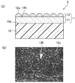
도 1 의 (a) 는, 본 발명의 일 실시형태에 의한 전자파 투과성 금속 광택 부재와, 이 금속 광택 부재를 사용한 전자파 투과성 금속 필름의 개략 단면도이고, 도 1 의 (b) 는, 본 발명의 일 실시형태에 의한 전자파 투과성 금속 광택 부재의 표면의 전자 현미경 사진이다.
도 2 는, 도 1 의 (b) 의 일부 영역에 있어서의 단면의 화상이다.1(a) is a schematic cross-sectional view of an electromagnetic wave-transmitting metallic luster member according to an embodiment of the present invention and an electromagnetic-wave-transmitting metallic film using the metallic luster member, and FIG. It is an electron micrograph of the surface of the electromagnetic wave-transmitting metallic luster member according to the embodiment.
FIG. 2 is an image of a cross section in a partial region of FIG. 1(b).
이하, 첨부 도면을 참조하면서, 본 발명의 하나의 바람직한 실시형태에 대해 설명한다. 이하에 있어서는, 설명의 편의를 위해서 본 발명의 바람직한 실시형태만을 나타내지만, 물론, 이것에 의해 본 발명을 한정하고자 하는 것은 아니다.Hereinafter, one preferred embodiment of the present invention will be described with reference to the accompanying drawings. In the following, only preferred embodiments of the present invention are shown for convenience of explanation, but, of course, the present invention is not intended to be limited thereto.
<1. 기본 구성><1. Basic configuration>
도 1 의 (a) 에, 본 발명의 일 실시형태에 의한 전자파 투과성 금속 광택 부재 (이하,「금속 광택 부재」라고 한다) (1) 와, 이 금속 광택 부재 (1) 를 사용한 전자파 투과성 금속 필름 (이하,「금속 필름」이라고 한다) (3) 의 개략 단면도를 나타내고, 또, 도 1 의 (b) 에, 본 발명의 일 실시형태에 의한 금속 광택 부재 (1) 의 표면의 전자 현미경 사진 (SEM 화상) 을 나타낸다. 또한, 전자 현미경 사진에 있어서의 화상 사이즈는 1.16 ㎛ × 0.85 ㎛ 이다.In Fig. 1(a), an electromagnetic wave-transmitting metallic luster member (hereinafter referred to as "metal luster member") according to an embodiment of the present invention (1) and an electromagnetic wave-transmitting metal film using this metallic luster member 1 (Hereinafter referred to as "metal film") A schematic cross-sectional view of (3) is shown, and in FIG. 1(b), an electron micrograph of the surface of the
금속 광택 부재 (1) 는, 적어도 산화인듐을 함유하는, 하지층으로서의 산화인듐 함유층 (11) 과, 이 산화인듐 함유층 (11) 상에 적층된 금속층 (12) 을 포함한다. 금속 필름 (3) 은, 이 금속 광택 부재 (1) 와 기재 필름 (10) 을 포함한다. 산화인듐 함유층 (11) 은, 금속 광택을 부여해야 하는 기재 필름 (10) 의 면에 형성되어 있다. 산화인듐 함유층 (11) 은, 기재 필름 (10) 의 면에 직접 형성되어 있어도 되고, 기재 필름 (10) 의 면에 형성한 보호막 등을 개재하여 간접적으로 형성되어도 된다. 산화인듐 함유층 (11) 은, 금속 광택을 부여해야 하는 기재 필름 (10) 의 면에 연속 상태로, 바꿔 말하면, 간극 없이 형성하는 것이 바람직하다. 연속 상태로 형성함으로써, 산화인듐 함유층 (11), 나아가서는, 금속 광택 부재 (1) 나 금속 필름 (3) 의 평활성이나 내식성을 향상시킬 수 있고, 또, 산화인듐 함유층 (11) 을 면내 불균일 없이 성막하는 것도 용이해진다.The
금속층 (12) 은 산화인듐 함유층 (11) 에 적층된다. 금속층 (12) 은 복수의 부분 (12a) 을 포함한다. 산화인듐 함유층 (11) 에 적층됨으로써, 이들 부분 (12a) 은, 적어도 일부에 있어서 서로 불연속의 상태, 바꿔 말하면, 적어도 일부에 있어서 간극 (12b) 에 의해 분리된다. 간극 (12b) 에 의해 분리되기 때문에, 이들 부분 (12a) 의 시트 저항은 커져, 전파와의 상호 작용이 저하되므로, 전파를 투과시킬 수 있다. 이들 각 부분 (12a) 은 금속을 증착, 스퍼터 등을 함으로써 형성된 스퍼터 입자의 집합체이다. 스퍼터 입자가 기재 필름 (10) 등의 기체 상에서 박막을 형성할 때에는, 기체 상에서의 입자의 표면 확산성이 박막의 형상에 영향을 미친다. 본 발명자들은, 예의 연구를 거듭한 결과, 기체 상에 산화인듐 함유층을 형성하고, 금속막의 표면 확산성을 촉진시킴으로써, 금속층을 불연속의 상태로 성장시키는 것에 성공하였다. 또한, 본 명세서에서 말하는「불연속의 상태」란, 간극 (12b) 에 의해 서로 분리되어 있고, 이 결과, 서로 전기적으로 절연되어 있는 상태를 의미한다. 전기적으로 절연됨으로써, 시트 저항이 커져, 원하는 전자파 투과성이 얻어지게 된다. 불연속의 형태는, 특별히 한정되는 것이 아니고, 예를 들어, 도상, 크랙 등이 포함된다. 여기서「도상」이란, 도 1 의 (b) 에 나타내어져 있는 바와 같이, 스퍼터 입자의 집합체인 입자끼리가 각각 독립되어 있고, 그들 입자가, 서로 조금 이간되거나 또는 일부 접촉된 상태에서 전면에 깔려서 이루어지는 구조를 의미한다.The
<2. 기재 필름 (기체)><2. Base film (gas)>
기재 필름 (10) 에는, 폴리에틸렌테레프탈레이트 (PET), 폴리에틸렌나프탈레이트 (PEN), 폴리부틸렌테레프탈레이트, 폴리아미드, 폴리염화비닐, 폴리카보네이트 (PC), 시클로올레핀 폴리머 (COP), 폴리스티렌, 폴리프로필렌 (PP), 폴리에틸렌, 폴리시클로올레핀, 폴리우레탄, 아크릴 (PMMA), ABS 등의 단독 중합체나 공중합체로 이루어지는 투명 필름을 사용할 수 있다. 이들 부재에 의하면, 광휘성이나 전자파 투과성에 영향을 주는 경우도 없다. 단, 산화인듐 함유층 (11) 이나 금속층 (12) 을 나중에 형성하는 관점에서, 증착이나 스퍼터 등의 고온에 견딜 수 있는 것인 것이 바람직하고, 따라서, 상기 재료 중에서도, 예를 들어, 폴리에틸렌테레프탈레이트, 폴리에틸렌나프탈레이트, 아크릴, 폴리카보네이트, 시클로올레핀 폴리머, ABS, 폴리프로필렌, 폴리우레탄이 바람직하다. 그 중에서도, 내열성과 비용의 밸런스가 양호한 점에서 폴리에틸렌테레프탈레이트나 시클로올레핀 폴리머, 폴리카보네이트, 아크릴이 바람직하다. 기재 필름 (10) 은, 단층 필름이어도 되고 적층 필름이어도 된다. 가공하기 용이함 등에서, 두께는, 예를 들어, 6 ㎛ ∼ 250 ㎛ 정도가 바람직하다. 산화인듐 함유층 (11) 과의 부착력을 강하게 하기 위해서, 플라즈마 처리나 접착 용이 처리 등이 실시되어도 된다.In the
여기서, 기재 필름 (10) 은, 본원 발명의 금속 광택 부재 (1) 를 부여할 수 있는 대상 (이하,「기체」라고 한다) 의 일례에 지나지 않는 점에 주의해야 한다. 기체에는, 기재 필름 (10) 이외에, 수지 성형물 기재, 유리 기재, 금속 광택을 부여해야 하는 물품 그 자체도 포함된다. 수지 성형 기재로는, 예를 들어, 자동차의 엠블럼용의 수지 등이 있다. 금속 광택을 부여해야 하는 물품으로는, 예를 들어, 스마트 키를 형성한 자동차의 도어 노브, 휴대 전화 케이스, PC 케이스, 냉장고 등이 있다. 본 발명의 금속 광택 부재 (1) 는, 이들 모든 기체에 부여할 수 있다. 이 경우, 금속 광택 부재 (1) 를 부여해야 하는 기체는, 상기의 기재 필름 (10) 과 동일한 재질, 조건을 만족하고 있는 것이 바람직하다.Here, it should be noted that the
<3. 산화인듐 함유층><3. Indium oxide containing layer>
산화인듐 함유층 (11) 으로서, 산화인듐 (In2O3) 그 자체를 사용할 수도 있고, 예를 들어, 인듐주석 산화물 (ITO) 이나, 인듐아연 산화물 (IZO) 과 같은 금속 함유물을 사용할 수도 있다. 단, 제 2 금속을 함유한 ITO 나 IZO 쪽이, 스퍼터링 공정에서의 방전 안정성이 높은 점에서, 보다 바람직하다. 이들 산화인듐 함유층 (11) 을 사용함으로써, 기체의 면을 따라 연속 상태의 막을 형성할 수도 있고, 또, 이 경우에는, 산화인듐 함유층 상에 적층되는 금속층을, 예를 들어, 도상의 불연속 구조로 할 수도 있다. 또한, 후술하는 바와 같이, 이 경우에는, 금속층에, 크롬 (Cr) 또는 인듐 (In) 뿐만 아니라, 통상적으로는 불연속 구조가 되기 어려워, 본 용도에는 적용이 어려웠던, 알루미늄 등의 다양한 금속을 함유시킬 수 있다. ITO 에 있어서의 In2O3 의 중량에 대한 주석 (Sn) 의 함유율은 특별히 한정되는 것은 아니지만, 예를 들어, 2.5 wt% ∼ 30 wt%, 보다 바람직하게는, 3 wt% ∼ 10 wt% 이다. 또, IZO 에 있어서의 In2O3 의 중량에 대한 산화아연 (ZnO) 의 함유율은, 예를 들어, 2 wt% ∼ 20 wt% 이다. 산화인듐 함유층 (11) 의 두께는, 시트 저항이나 전파 투과성, 생산성의 관점에서, 통상 1000 ㎚ 이하가 바람직하고, 50 ㎚ 이하가 보다 바람직하고, 20 ㎚ 이하가 더욱 바람직하다. 한편, 적층되는 금속층 (12) 이 불연속 상태가 되도록, 1 ㎚ 이상인 것이 바람직하고, 확실하게 불연속 상태로 하기 위해서 2 ㎚ 이상인 것이 보다 바람직하고, 5 ㎚ 이상인 것이 더욱 바람직하다.As the indium oxide-containing
<4. 금속층><4. Metal layer>
금속층 (12) 은, 충분한 광휘성을 발휘할 수 있는 것은 물론, 융점이 비교적 낮은 것인 것이 바람직하다. 금속층 (12) 은, 스퍼터링을 사용한 박막 성장에 의해 부여되기 때문이다. 이와 같은 이유로부터, 금속층 (12) 으로는, 융점이 약 1000 ℃ 이하인 금속이 적합하고, 예를 들어, 알루미늄 (Al), 아연 (Zn), 납 (Pb), 구리 (Cu), 은 (Ag) 에서 선택된 적어도 1 종의 금속, 및 그 금속을 주성분으로 하는 합금 중 어느 것을 함유하는 것이 바람직하다. 특히, 물질의 광휘성이나 안정성, 가격 등의 이유로부터 Al 및 그것들의 합금이 바람직하다.It is preferable that the
금속층 (12) 의 두께는, 충분한 광휘성을 발휘하도록, 통상 20 ㎚ 이상이 바람직하고, 한편, 시트 저항이나 전파 투과성의 관점에서, 통상 100 ㎚ 이하가 바람직하다. 예를 들어, 20 ㎚ ∼ 100 ㎚ 가 바람직하고, 30 ㎚ ∼ 70 ㎚ 가 보다 바람직하다. 이 두께는, 균일한 막을 양호한 생산성으로 형성하는 데에도 적합하고, 또, 최종 제품인 수지 성형품의 볼품도 양호하다.The thickness of the
또, 동일한 이유로부터, 금속층의 두께와 산화인듐 함유층 두께의 비 (금속층의 두께/산화인듐 함유층의 두께) 는, 0.1 ∼ 100 의 범위가 바람직하고, 0.3 ∼ 35 의 범위가 보다 바람직하다.Further, for the same reason, the ratio of the thickness of the metal layer to the thickness of the indium oxide-containing layer (thickness of the metal layer/thickness of the indium oxide-containing layer) is preferably in the range of 0.1 to 100, and more preferably in the range of 0.3 to 35.
또한, 금속층과 산화인듐 함유층의 적층체로서의 시트 저항은, 100 ∼ 100000 Ω/□ 인 것이 바람직하다. 이 경우, 전파 투과성은, 1 ㎓ 의 파장에 있어서, 10 ∼ 0.01[-dB]정도가 된다. 더욱 바람직하게는, 1000 ∼ 50000 Ω/□ 이다. 이 시트 저항의 값은, 금속층의 재질이나 두께는 물론, 하지층인 산화인듐 함유층의 재질이나 두께로부터도 큰 영향을 받는다. 따라서, 산화인듐 함유층과의 관계도 고려한 후에 설정할 필요가 있다.Further, the sheet resistance as a laminate of the metal layer and the indium oxide-containing layer is preferably from 100 to 100000 Ω/□. In this case, the radio wave transmittance is about 10 to 0.01 [-dB] at a wavelength of 1 GHz. More preferably, it is 1000 to 50000 Ω/□. The value of the sheet resistance is greatly influenced not only by the material and thickness of the metal layer, but also by the material and thickness of the indium oxide-containing layer as the underlying layer. Therefore, it is necessary to set it after considering the relationship with the indium oxide-containing layer as well.
<5. 금속층이 불연속 상태가 되는 메커니즘><5. Mechanism in which the metal layer becomes discontinuous>
산화인듐 함유층 (11) 을 형성하지 않고, 기체 상에 직접적으로 금속층 (12) 을 성막한 경우, 금속층 (12) 은 기체 (10) 상에서 연속 상태가 되어 버린다. 이 경우, 충분한 광휘성은 얻어지지만, 시트 저항은 매우 작아지고, 따라서, 전파 투과성을 확보할 수는 없다. 이에 반해, 기체 상에 성막한 산화인듐 함유층 (11) 상에 금속층 (12) 을 적층한 경우, 예를 들어 연속 상태로 형성된 산화인듐 함유층 (11) 상에서, 금속층 (12) 은 불연속의 상태로 형성되고, 이 결과, 충분한 광휘성이 얻어지는 것은 물론, 전파 투과성을 확보할 수도 있다. 금속층 (12) 이 산화인듐 함유층 (11) 상에서 불연속 상태가 되는 메커니즘의 상세한 것은 반드시 분명한 것은 아니지만, 대체로, 다음과 같은 것이라고 추측된다. 즉, 금속층 (12) 의 박막 형성 프로세스에 있어서, 불연속 구조의 형성하기 용이함은, 금속층 (12) 이 부여되는 피부여 부재 (본건에서는, 산화인듐 함유층 (11)) 상에서의 표면 확산과 관련성이 있어, 피부여 부재의 온도가 높고, 피부여 부재에 대한 금속층의 젖음성이 작으며, 금속층의 재료의 융점이 낮은 쪽이 불연속 구조를 형성하기 쉽다는 것이다. 따라서, 이하의 실시예에서 특별히 사용한 알루미늄 (Al) 이외의 금속에 대해서도, 아연 (Zn), 납 (Pb), 구리 (Cu), 은 (Ag) 등의 비교적 융점이 낮은 금속에 대해서는, 동일한 수법으로 불연속 구조를 형성할 수 있을 것으로 생각된다.When the
<6. 금속 광택 부재의 제조><6. Manufacturing of metallic luster member>
금속 광택 부재 (1) 의 제조 방법의 일례에 대해, 기체로서 기재 필름 (10) 을 사용한 경우, 즉, 금속 필름 (3) 을 제조하는 경우를 예로 들어 설명한다. 특별히 설명하지 않지만, 기재 필름 (10) 이외의 기체를 사용한 경우에 대해서도 동일한 방법으로 제조할 수 있다.About an example of the manufacturing method of the
(1) 산화인듐 함유층을 성막하는 공정(1) Step of forming an indium oxide-containing layer
기재 필름 (10) 에 대해, 산화인듐 함유층 (11) 을 성막한다. 산화인듐 함유층 (11) 은, 진공 증착, 스퍼터링, 이온 플레이팅 등에 의해 형성할 수 있다. 단, 대면적에서도 두께를 엄밀하게 제어할 수 있는 점에서, 스퍼터링이 바람직하다.With respect to the
(2) 금속층을 적층하는 공정(2) The process of laminating a metal layer
이어서, 산화인듐 함유층 (11) 상에 금속층 (12) 을 적층한다. 이 경우에도, 예를 들어, 스퍼터링을 사용할 수 있다. 또한, 산화인듐 함유층 (11) 과 금속층 (12) 사이에는, 다른 층을 개재시키지 않고 직접 접촉시키는 것이 바람직하다. 단, 상기에 설명한 산화인듐 함유층 (11) 상에 있어서의 금속층 (12) 의 표면 확산의 메커니즘이 확보되는 것이라면, 다른 층을 개재시킬 수도 있다.Next, a
<7. 실시예><7. Example>
이하, 실시예 및 비교예를 들어, 본 발명을 보다 구체적으로 설명한다. 금속 필름 (3) 에 관해서 각종 시료를 준비하고, 시트 저항, 전파 투과 감쇠량, 및 가시광 반사율을 평가하였다. 시트 저항과 전파 투과 감쇠량은, 전파 투과성에 관한 평가, 가시광 반사율은, 광휘성에 관한 평가이다. 가시광 반사율과 시트 저항의 값은 큰 쪽이 바람직하고, 전파 투과 감쇠량의 값은 작은 쪽이 바람직하다.Hereinafter, the present invention will be described in more detail with reference to Examples and Comparative Examples. Various samples were prepared for the
평가 방법의 상세한 것은 이하와 같다.The details of the evaluation method are as follows.
(1) 시트 저항(1) sheet resistance
냅슨사 제조 비접촉식 저항 측정 장치 NC-80MAP 를 사용하고, JIS-Z 2316 에 준거하여, 와전류 측정법에 의해 금속층과 산화인듐 함유층의 적층체로서의 시트 저항을 측정하였다.The sheet resistance as a laminate of a metal layer and an indium oxide-containing layer was measured by an eddy current measurement method in accordance with JIS-Z 2316 using a non-contact resistance measuring device NC-80MAP manufactured by Napson Corporation.
이 시트 저항은, 100 Ω/□ 이상인 것이 필요하고, 200 Ω/□ 이상인 것이 바람직하고, 또한 600 Ω/□ 이상인 것이 보다 바람직하다. 100 Ω/□ 보다 작으면, 충분한 전파 투과성이 얻어지지 않는다는 문제가 있다.This sheet resistance is required to be 100 Ω/□ or more, preferably 200 Ω/□ or more, and more preferably 600 Ω/□ or more. If it is less than 100 Ω/□, there is a problem that sufficient radio wave transmittance cannot be obtained.
(2) 전파 투과 감쇠량(2) Radio wave transmission attenuation
1 ㎓ 에 있어서의 전파 투과 감쇠량을 KEC 법 측정 평가 지그 및 애질런트사 제조 스펙트럼 애널라이저 CXA signal Analyzer NA9000A 를 사용하여 평가하였다. 밀리파 레이더의 주파수 대역 (76 ∼ 80 ㎓) 에 있어서의 전자파 투과성과, 마이크로파 대역 (1 ㎓) 에 있어서의 전자파 투과성에는 상관성이 있어, 비교적 가까운 값을 나타내는 점에서, 이번 평가에서는, 마이크로파 대역 (1 ㎓) 에 있어서의 전자파 투과성, 즉, 마이크로파 전계 투과 감쇠량을 지표로 하였다.The amount of radio wave transmission attenuation in 1 GHz was evaluated using a KEC method measurement evaluation jig and an Agilent spectrum analyzer CXA signal analyzer NA9000A. Since there is a correlation between the electromagnetic wave transmittance in the frequency band (76 to 80 GHz) of the milliwave radar and the electromagnetic wave transmittance in the microwave band (1 GHz), and shows a relatively close value, in this evaluation, the microwave band ( The electromagnetic wave transmittance in 1 GHz), that is, the amount of microwave electric field transmission attenuation was used as an index.
이 마이크로파 전계 투과 감쇠량은, 10[-dB]이하인 것이 필요하고, 5[-dB]이하인 것이 바람직하고, 2[-dB]이하인 것이 보다 바람직하다. 10[-dB]이상이면, 90 % 이상의 전파가 차단된다는 문제가 있다.The microwave electric field transmission attenuation amount is required to be 10 [-dB] or less, preferably 5 [-dB] or less, and more preferably 2 [-dB] or less. If it is 10 [-dB] or more, there is a problem that 90% or more of radio waves are blocked.
(3) 가시광 반사율(3) visible light reflectance
히타치 하이테크놀로지즈사 제조 분광 광도계 U4100 을 사용하여, 550 ㎚ 의 측정 파장에 있어서의 반사율을 측정하였다. 기준으로서, Al 증착 미러의 반사율을 반사율 100 % 로 하였다.The reflectance in the measurement wavelength of 550 nm was measured using the spectrophotometer U4100 manufactured by Hitachi High Technologies. As a reference, the reflectance of the Al vapor deposition mirror was set to 100% reflectance.
이 가시광 반사율은, 충분한 광휘성을 갖기 위해 20 % 이상이 필요하고, 40 % 이상인 것이 바람직하고, 더욱 바람직하게는 50 % 이상이다. 가시광 반사율이, 20 % 보다 작으면, 광휘성이 저하되어, 외관이 우수하지 않다는 문제가 있다.In order to have sufficient luminance, this visible light reflectance is required to be 20% or more, preferably 40% or more, and more preferably 50% or more. When the visible light reflectance is less than 20%, there is a problem that the luminance decreases and the appearance is not excellent.
이하의 표 1 에, 평가 결과를 나타낸다.In Table 1 below, the evaluation results are shown.

[실시예 1][Example 1]
기재 필름으로서, 미츠비시 수지사 제조 PET 필름 (두께 125 ㎛) 을 사용하였다.As the base film, a PET film (125 µm in thickness) manufactured by Mitsubishi Resin Company was used.
먼저, DC 마그네트론 스퍼터링을 사용하여, 기재 필름의 면을 따라, 50 ㎚ 두께의 ITO 층을 그 위에 직접 형성하였다. ITO 층을 형성할 때의 기재 필름의 온도는, 130 ℃ 로 설정하였다. ITO 는, In2O3 에 대해 Sn 을 10 wt% 함유시킨 것이다.First, using DC magnetron sputtering, along the side of the base film, a 50 nm thick ITO layer was directly formed thereon. The temperature of the base film when forming the ITO layer was set to 130°C. ITO contained 10 wt% of Sn with respect to In 2 O 3.
이어서, 교류 스퍼터링 (AC : 40 ㎑) 을 사용하여, ITO 층 상에, 50 ㎚ 두께의 알루미늄 (Al) 층을 형성하고, 금속 광택 부재 (금속 필름) 를 얻었다. Al 층을 형성할 때의 기재 필름의 온도는, 130 ℃ 로 설정하였다.Next, an aluminum (Al) layer having a thickness of 50 nm was formed on the ITO layer using alternating current sputtering (AC: 40 kHz), and a metallic luster member (metal film) was obtained. The temperature of the base film when forming the Al layer was set to 130°C.
도 1 의 (b) 는, 이들 처리의 결과 얻어진 금속 광택 부재 (금속 필름) 표면의 전자 현미경 사진 (SEM 화상) 이고, 도 2 는, 이 도 1 의 (b) 의 일부 영역에 있어서의 단면의 화상이다. 또한, 도 2 의 전자 현미경 사진에 있어서의 화상 사이즈는 1.16 ㎛ × 0.85 ㎛ 이다.FIG. 1(b) is an electron micrograph (SEM image) of the surface of a metallic luster member (metal film) obtained as a result of these treatments, and FIG. 2 is a cross-sectional view in a partial region of FIG. 1(b). It's a burn. In addition, the image size in the electron micrograph of FIG. 2 is 1.16 µm x 0.85 µm.
이들 도면으로부터 분명한 바와 같이, 본 실시예에서는, 금속 광택 부재의 ITO 층은, 기재 필름의 면을 따라 연속 상태로 형성되어 있으므로 높은 평활성과 내식성을 발휘하고, 그 한편으로, 알루미늄층은, ITO 층에 적층됨으로써 불연속인 상태로 형성된 복수의 부분 (12a) 을 포함하므로, 그 시트 저항은 260 Ω/□ 이 되고, 그 전파 투과 감쇠량은 1 ㎓ 의 파장에 있어서 4.5[-dB]가 되어, 전파 투과성에 대해 양호한 결과가 얻어졌다. 또한, 표 1 에서는, 편의상, 전파 투과 감쇠량의「평가」결과로서, 당해 전파 투과 감쇠량이 2[-dB]보다 작은 경우를「◎」로, 2[-dB]이상이고 또한 5[-dB]보다 작은 경우를「○」로, 5[-dB]이상이고 또한 10[-dB]보다 작은 경우를「△」로, 10[-dB]이상을「×」로, 각각 나타내고 있다.As is clear from these drawings, in this embodiment, the ITO layer of the metallic luster member is formed in a continuous state along the surface of the base film, thus exhibiting high smoothness and corrosion resistance. On the other hand, the aluminum layer is an ITO layer. Since it includes a plurality of
또, 이 금속 광택 부재의 가시광 반사율은 56 % 가 되어, 광휘성에 대해서도 양호한 결과가 얻어졌다. 또한, 편의상, 표 1 에서는, 가시광 반사율의「평가」결과로서, 당해 가시광 반사율이 50 % 보다 큰 경우를「◎」로, 50 % 이하이고 또한 40 % 보다 큰 경우를「○」로, 40 % 이하이고 또한 20 % 보다 큰 경우를「△」로, 20 % 이하를「×」로, 각각 나타내고 있다. 또한, 전파 투과성과 광휘성의「종합 평가」로서, 양자가 동일한 평가 결과인 경우에는 동일한 평가 결과를, 일방이 다른 한쪽보다 나쁜 결과인 경우에는 나쁜 쪽의 평가 결과를, 각각 나타내고 있다. 결과적으로, 실시예 1 에 대해, 종합 평가는「○」가 되어, 전파 투과성과 광휘성의 쌍방을 겸비한 양호한 금속 광택 부재, 혹은, 금속 필름이 얻어졌다.Moreover, the visible light reflectance of this metallic luster member was 56 %, and favorable results were obtained also in luminance. In addition, for convenience, in Table 1, as a result of "evaluation" of visible light reflectance, a case where the visible light reflectance is greater than 50% is referred to as "◎", and a case where it is 50% or less and greater than 40% is referred to as "○", and 40%. The cases below and greater than 20% are indicated by "Δ", and 20% or less are indicated by "x", respectively. In addition, as "comprehensive evaluation" of radio wave transmittance and luminance, when both are the same evaluation results, the same evaluation results are shown, and when one is a worse result than the other, the bad evaluation results are shown. As a result, with respect to Example 1, the comprehensive evaluation became "(circle)", and a good metallic luster member or metallic film having both radio wave transmittance and luminance was obtained.
[실시예 2] ∼ [실시예 4][Example 2]-[Example 4]
ITO 층 상에 적층하는 알루미늄층의 두께를, 실시예 2, 3 에 대해서는 실시예 1 의 그것보다 얇아지도록 변경하고, 한편, 실시예 4 에 대해서는 실시예 1 의 그것보다 두꺼워지도록 변경하였다. 그 밖의 조건에 대해서는 실시예 1 과 동일하다.The thickness of the aluminum layer laminated on the ITO layer was changed to be thinner than that of Example 1 for Examples 2 and 3, while the thickness of Example 4 was changed to be thicker than that of Example 1. Other conditions are the same as in Example 1.
이 경우, 시트 저항 및 전파 투과 감쇠량에 대해서는 실시예 2 ∼ 실시예 4 의 전부에 있어서, 실시예 1 과 동일한 값 및 결과가 얻어졌다. 한편, 가시광 반사율에 대해서는, 알루미늄층의 두께가 실시예 1 의 그것보다 얇은 실시예 2, 3 에 대해서는 약간 열등한 결과가 되었지만, 실시예 4 에 대해서는 실시예 1 보다 양호한 결과가 얻어졌다. 단, 실시예 2, 3 에 대해서도, 실용에 충분히 견딜 수 있는 것이다.In this case, about the sheet resistance and the amount of radio wave transmission attenuation, in all of Examples 2 to 4, the same values and results as in Example 1 were obtained. On the other hand, with respect to the visible light reflectance, the results were slightly inferior to Examples 2 and 3 in which the thickness of the aluminum layer was thinner than that of Example 1, but for Example 4, better results were obtained than those of Example 1. However, also about Examples 2 and 3, it can withstand practical use sufficiently.
[실시예 5] ∼ [실시예 8][Example 5]-[Example 8]
ITO 층의 두께를 실시예 1 보다 얇아지도록 설정하였다. 그 밖의 조건에 대해서는 실시예 1 과 동일하다.The thickness of the ITO layer was set to be thinner than that of Example 1. Other conditions are the same as in Example 1.
이 경우, 시트 저항 및 전파 투과 감쇠량에 대해서는 실시예 5 ∼ 실시예 8 의 전부에 있어서, 실시예 1 보다 양호한 결과가 얻어졌다. 또, 가시광 반사율에 대해서는 실시예 5 ∼ 실시예 8 의 전부에 있어서, 실시예 1 과 동일한 값 및 결과가 얻어졌다. 이들 실시예에 의해, ITO 층의 두께는 얇아도 되는 것이 분명해져, ITO 층의 두께를 얇게 함으로써, 재료 비용을 억제할 수 있는 것이 분명해졌다.In this case, with respect to the sheet resistance and the amount of radio wave transmission attenuation, in all of Examples 5 to 8, results better than those of Example 1 were obtained. In addition, about the visible light reflectance, in all of Examples 5 to 8, the same values and results as in Example 1 were obtained. By these Examples, it became clear that the thickness of the ITO layer may be thin, and it became clear that the material cost can be suppressed by making the thickness of the ITO layer thin.
[실시예 9] ∼ [실시예 12][Example 9]-[Example 12]
ITO 층에 있어서의 Sn 의 함유율을, 실시예 9 에 대해서는 실시예 1 의 그것보다 커지도록 변경하고, 한편, 실시예 10 내지 12 에 대해서는 실시예 1 의 그것보다 작아지도록 변경하였다. 또한, 실시예 12 의 ITO 층에서는 Sn 을 제로로 하고 있으므로, 보다 정확하게는, ITO 층이 아니라, 산화인듐 (In2O3) 층으로 되어 있다. 그 외에, 실시예 12 에서는, 알루미늄층은 40 ㎚ 로 하였다. 그 밖의 조건에 대해서는 실시예 1 과 동일하다.The content rate of Sn in the ITO layer was changed to be larger than that of Example 1 for Example 9, and changed to be smaller than that of Example 1 for Examples 10 to 12. In addition, since Sn is zero in the ITO layer of Example 12, more precisely, it is not an ITO layer, but an indium oxide (In 2 O 3 ) layer. In addition, in Example 12, the aluminum layer was set to 40 nm. Other conditions are the same as in Example 1.
이 경우, 시트 저항 및 전파 투과 감쇠량에 대해서는 실시예 9 ∼ 실시예 11 에 있어서, 실시예 1 과 동일한 결과가 얻어지고, 실시예 12 에 있어서는, 실시예 1 보다 약간 열등한 결과가 되었다. 또, 가시광 반사율에 대해서는 실시예 9 ∼ 실시예 11 에 있어서, 실시예 1 과 동일한 값 및 결과가 얻어지고, 실시예 12 에 있어서, 실시예 1 보다 약간 열등한 결과가 되었다. 이 결과로부터, ITO 층은, Sn 을 함유하는 것이 보다 바람직한 것이 분명해졌다.In this case, about the sheet resistance and the amount of radio wave transmission attenuation, in Examples 9 to 11, the same results as in Example 1 were obtained, and in Example 12, the results were slightly inferior to those of Example 1. In addition, with respect to visible light reflectance, in Examples 9 to 11, the same values and results as in Example 1 were obtained, and in Example 12, the result was slightly inferior to that of Example 1. From this result, it became clear that it is more preferable that an ITO layer contains Sn.
[실시예 13][Example 13]
ITO 가 아니고, 산화인듐에 ZnO 를 함유시킨 IZO 를 사용하였다. ZnO 는, In2O3 에 대해 11 wt% 함유한다. 그 밖의 조건에 대해서는 실시예 1 과 동일하다.Instead of ITO, IZO containing ZnO in indium oxide was used. ZnO contains 11 wt% with respect to In 2 O 3. Other conditions are the same as in Example 1.
이 경우, 시트 저항 및 전파 투과 감쇠량에 대해서는 실시예 1 보다 약간 열등한 결과가 되었다. 한편, 가시광 반사율에 대해서는 실시예 1 과 동일한 값 및 결과가 얻어졌다. 실시예 1 보다 종합 평가는 열등하지만, ZnO 를 함유시킨 경우에도, 충분히 실용 가능한 것이 분명해졌다.In this case, the sheet resistance and the amount of radio wave transmission attenuation were slightly inferior to those of Example 1. On the other hand, about the visible light reflectance, the same values and results as in Example 1 were obtained. Comprehensive evaluation is inferior to Example 1, but it has become clear that even when ZnO is contained, it is sufficiently practical.
[비교예 1][Comparative Example 1]
ITO 층 상에 적층하는 알루미늄층의 두께를, 실시예 1 의 그것보다 두꺼워지도록 변경하였다. 그 밖의 조건에 대해서는 실시예 1 과 동일하다.The thickness of the aluminum layer laminated on the ITO layer was changed to be thicker than that of Example 1. Other conditions are the same as in Example 1.
이 경우, 가시광 반사율에 대해서는, 두께를 늘린 만큼, 실시예 1 보다 양호한 결과가 얻어졌다. 한편, 시트 저항 및 전파 투과 감쇠량에 대해서는 실시예 1 의 그것들보다 크게 열등한 결과가 되어, 실용 불가능한 것이 되었다.In this case, about the visible light reflectance, the result was obtained better than that of Example 1 by increasing the thickness. On the other hand, the sheet resistance and the amount of radio wave transmission attenuation were significantly inferior to those of Example 1, and were impractical.
[비교예 2][Comparative Example 2]
ITO 층을 형성하지 않고, 기재 필름 상에 알루미늄층을 직접 성막하였다. 그 밖의 조건에 대해서는 실시예 1 과 동일하다.Without forming an ITO layer, an aluminum layer was directly formed on the base film. Other conditions are the same as in Example 1.
이 경우, 가시광 반사율에 대해서는, 실시예 1 과 동일한 값 및 결과가 얻어졌지만, 시트 저항 및 전파 투과 감쇠량에 대해서는, 실시예 1 의 그것들보다 크게 열등한 결과가 되어, 실용 불가능한 것이 되었다.In this case, for the visible light reflectance, the same values and results as in Example 1 were obtained, but the sheet resistance and the amount of radio wave transmission attenuation were significantly inferior to those of Example 1, and thus it was impractical.
<8. 금속 박막의 이용><8. Use of metal thin film>
금속 광택 부재 (1) 에 형성된 금속층 (12) 은, 두께 20 ㎚ ∼ 100 ㎚ 정도의 얇은 것으로서, 이것만을 금속 박막으로서 사용할 수도 있다. 예를 들어, 기재 필름 (10) 과 같은 기체에 적층된 인듐 산화물 함유층 (11) 상에, 스퍼터링으로 금속층 (12) 을 형성하여, 필름을 얻는다. 또, 이것과는 별도로, 접착제를 기재 상에 도공하여 접착제층이 형성된 기재를 제작한다. 필름과 기재를, 금속층 (12) 과 접착제층이 접하도록 첩합 (貼合) 시키고, 충분히 밀착시킨 후에 필름과 기재를 박리시킴으로써, 필름의 최표면에 존재한 금속층 (금속 박막) (12) 을 기재의 최표면에 전사시킬 수 있다.The
본 발명은 상기 실시예에 한정되는 것이 아니고, 발명의 취지로부터 일탈하지 않는 범위에서 적절히 변경하여 구체화할 수도 있다.The present invention is not limited to the above examples, and may be appropriately changed and embodied within a range not departing from the spirit of the invention.
산업상 이용가능성Industrial applicability
본 발명에 관련된 금속 필름이나 금속 광택 부재는, 예를 들어, 프런트 그릴, 엠블럼과 같은 자동차의 프런트 부분에 탑재되는 밀리파 레이더의 커버 부재를 장식하기 위해서 바람직하게 사용할 수 있다. 또, 예를 들어, 휴대 전화나 스마트 폰, 태블릿형 PC, 노트형 PC, 냉장고 등, 의장성과 전자파 투과성의 쌍방이 요구되는 다양한 용도에도 이용할 수 있다.The metal film or metallic luster member according to the present invention can be preferably used to decorate a cover member of a milliwave radar mounted on a front portion of an automobile, such as a front grill or an emblem, for example. Further, for example, it can be used in various applications requiring both design and electromagnetic wave transmission, such as a mobile phone, a smart phone, a tablet PC, a notebook PC, and a refrigerator.
1 : 금속 광택 부재
3 : 금속 필름
10 : 기재 필름
11 : 산화인듐 함유층
12 : 금속층1: metallic luster member
3: metal film
10: base film
11: indium oxide-containing layer
12: metal layer
Claims (13)
상기 산화인듐 함유층은 연속 상태로 형성되어 있는 전자파 투과성 금속 광택 부재.The method of claim 1,
The electromagnetic wave-transmitting metallic luster member in which the indium oxide containing layer is formed in a continuous state.
상기 산화인듐 함유층은, 산화인듐 (In2O3), 인듐주석 산화물 (ITO), 또는 인듐아연 산화물 (IZO) 중 어느 것인 전자파 투과성 금속 광택 부재.The method according to claim 1 or 2,
The indium oxide-containing layer is an electromagnetic wave-transmitting metallic luster member of any of indium oxide (In 2 O 3 ), indium tin oxide (ITO), or indium zinc oxide (IZO).
상기 산화인듐 함유층의 두께는, 1 ㎚ ∼ 1000 ㎚ 인 전자파 투과성 금속 광택 부재.The method according to any one of claims 1 to 3,
The electromagnetic wave-transmitting metallic luster member having a thickness of the indium oxide-containing layer of 1 nm to 1000 nm.
상기 금속층의 두께는, 20 ㎚ ∼ 100 ㎚ 인 전자파 투과성 금속 광택 부재.The method according to any one of claims 1 to 4,
An electromagnetic wave-transmitting metallic luster member having a thickness of the metal layer of 20 nm to 100 nm.
상기 금속층의 두께와 상기 산화인듐 함유층 두께의 비 (상기 금속층의 두께/상기 산화인듐 함유층의 두께) 는, 0.02 ∼ 100 인 전자파 투과성 금속 광택 부재.The method according to any one of claims 1 to 5,
The ratio of the thickness of the metal layer to the thickness of the indium oxide-containing layer (thickness of the metal layer/thickness of the indium oxide-containing layer) is 0.02 to 100.
상기 금속층과 산화인듐 함유층의 적층체로서의 시트 저항은, 100 ∼ 100000 Ω/□ 인 전자파 투과성 금속 광택 부재.The method according to any one of claims 1 to 6,
An electromagnetic wave-transmitting metallic luster member having a sheet resistance of 100 to 100000 Ω/□ as a laminate of the metal layer and the indium oxide-containing layer.
상기 부분은 도상으로 형성되어 있는 전자파 투과성 적층 부재.The method according to any one of claims 1 to 7,
The electromagnetic wave-transmitting laminated member is formed in an island shape.
상기 금속층은, 알루미늄 (Al), 아연 (Zn), 납 (Pb), 구리 (Cu), 은 (Ag), 또는 이것들의 합금 중 어느 것인 전자파 투과성 금속 광택 부재.The method according to any one of claims 1 to 8,
The metal layer is aluminum (Al), zinc (Zn), lead (Pb), copper (Cu), silver (Ag), or any of alloys thereof.
상기 기체는, 기재 필름, 수지 성형물 기재, 유리 기재, 또는 금속 광택을 부여해야 하는 물품 중 어느 것인 전자파 투과성 금속 광택 부재.The method according to any one of claims 1 to 9,
The base material is a base film, a resin molded product base, a glass base material, or an electromagnetic wave-transmitting metallic luster member in any of an article to be given a metallic luster.
상기 금속층은, 알루미늄 (Al), 아연 (Zn), 납 (Pb), 구리 (Cu), 은 (Ag), 또는 이것들의 합금 중 어느 것인 전자파 투과성 금속 광택 부재.The method of claim 12,
The metal layer is aluminum (Al), zinc (Zn), lead (Pb), copper (Cu), silver (Ag), or any of alloys thereof.
Applications Claiming Priority (3)
| Application Number | Priority Date | Filing Date | Title |
|---|---|---|---|
| JPJP-P-2016-208000 | 2016-10-24 | ||
| JP2016208000A JP6400062B2 (en) | 2016-10-24 | 2016-10-24 | Electromagnetic wave transmitting metallic luster member, article using the same, and metallic thin film |
| PCT/JP2017/038354 WO2018079547A1 (en) | 2016-10-24 | 2017-10-24 | Electromagnetic wave-permeable shiny metal member, article using same, and metal thin film |
Related Parent Applications (1)
| Application Number | Title | Priority Date | Filing Date |
|---|---|---|---|
| KR1020197014865A Division KR20190061091A (en) | 2016-10-24 | 2017-10-24 | An electromagnetic wave-permeable metal luster member, an article using the same, and a metal thin film |
Publications (1)
| Publication Number | Publication Date |
|---|---|
| KR20210045527A true KR20210045527A (en) | 2021-04-26 |
Family
ID=62023596
Family Applications (3)
| Application Number | Title | Priority Date | Filing Date |
|---|---|---|---|
| KR1020197014909A KR102271407B1 (en) | 2016-10-24 | 2017-10-24 | Metallic lustrous member with electromagnetic wave transmissibility, article using the member, and metal thin film |
| KR1020217011568A KR20210045527A (en) | 2016-10-24 | 2017-10-24 | Metallic lustrous member with electromagnetic wave transmissibility, article using the member, and metal thin film |
| KR1020197014865A KR20190061091A (en) | 2016-10-24 | 2017-10-24 | An electromagnetic wave-permeable metal luster member, an article using the same, and a metal thin film |
Family Applications Before (1)
| Application Number | Title | Priority Date | Filing Date |
|---|---|---|---|
| KR1020197014909A KR102271407B1 (en) | 2016-10-24 | 2017-10-24 | Metallic lustrous member with electromagnetic wave transmissibility, article using the member, and metal thin film |
Family Applications After (1)
| Application Number | Title | Priority Date | Filing Date |
|---|---|---|---|
| KR1020197014865A KR20190061091A (en) | 2016-10-24 | 2017-10-24 | An electromagnetic wave-permeable metal luster member, an article using the same, and a metal thin film |
Country Status (7)
| Country | Link |
|---|---|
| US (1) | US11383478B2 (en) |
| EP (1) | EP3536495A4 (en) |
| JP (1) | JP6400062B2 (en) |
| KR (3) | KR102271407B1 (en) |
| CN (1) | CN109890608A (en) |
| TW (1) | TWI791466B (en) |
| WO (1) | WO2018079547A1 (en) |
Families Citing this family (28)
| Publication number | Priority date | Publication date | Assignee | Title |
|---|---|---|---|---|
| WO2019139156A1 (en) * | 2018-01-12 | 2019-07-18 | 日東電工株式会社 | Layered body |
| WO2019139122A1 (en) * | 2018-01-12 | 2019-07-18 | 日東電工株式会社 | Radio wave-transmitting lustrous metal member, article using same, and method for producing same |
| JP2019123238A (en) * | 2018-01-12 | 2019-07-25 | 日東電工株式会社 | Radio wave-transmitting metal lustrous member, article using the same, and method for producing the same |
| JP6980537B2 (en) * | 2018-01-12 | 2021-12-15 | 株式会社ウェーブロック・アドバンスト・テクノロジー | Metal layer holding film, metal-like decorative sheet intermediate, metal-like decorative sheet, extrusion laminated body, metal-like molded body, injection molded body, manufacturing method of metal-like molded body, manufacturing method of injection molded body and extrusion laminating How to make a body |
| WO2019208493A1 (en) * | 2018-04-23 | 2019-10-31 | 日東電工株式会社 | Electromagnetic-wave-permeable metallic-luster article, and decorative member |
| CN112020423B (en) * | 2018-04-23 | 2023-07-28 | 日东电工株式会社 | Electromagnetic wave-transparent metallic glossy article and metallic film |
| KR20210005586A (en) * | 2018-04-23 | 2021-01-14 | 닛토덴코 가부시키가이샤 | Electromagnetically transparent metallic polished articles |
| WO2019208499A1 (en) * | 2018-04-23 | 2019-10-31 | 日東電工株式会社 | Electromagnetically permeable article with metallic gloss |
| WO2019208490A1 (en) * | 2018-04-23 | 2019-10-31 | 日東電工株式会社 | Electromagnetic wave-permeable metal glossy article and method for manufacturing same |
| WO2019208504A1 (en) * | 2018-04-23 | 2019-10-31 | 日東電工株式会社 | Electromagnetic wave transparent metallic luster article, and metal thin film |
| CN112020422A (en) * | 2018-04-23 | 2020-12-01 | 日东电工株式会社 | Electromagnetic wave-permeable metallic luster article and decorative member |
| KR20210005575A (en) * | 2018-04-23 | 2021-01-14 | 닛토덴코 가부시키가이샤 | Electromagnetic wave-transmitting metallic luster article, and metallic thin film |
| JP2019188809A (en) * | 2018-04-23 | 2019-10-31 | 日東電工株式会社 | Electromagnetic wave transmissible metallic sheen article |
| WO2019208494A1 (en) * | 2018-04-23 | 2019-10-31 | 日東電工株式会社 | Electromagnetic wave transmissive metallic luster product and metal thin film |
| WO2019208488A1 (en) * | 2018-04-23 | 2019-10-31 | 日東電工株式会社 | Electromagnetic wave transmissive metal luster article |
| KR20210005576A (en) * | 2018-04-23 | 2021-01-14 | 닛토덴코 가부시키가이샤 | Electromagnetically transparent metallic polished articles |
| WO2019208489A1 (en) * | 2018-04-23 | 2019-10-31 | 日東電工株式会社 | Electromagnetic wave-transmitting metallic-luster article |
| JPWO2019230955A1 (en) * | 2018-06-01 | 2021-07-29 | 大日本印刷株式会社 | Metal-like decoration member and metal-like decoration molded body using it |
| WO2020067052A1 (en) * | 2018-09-25 | 2020-04-02 | 積水化学工業株式会社 | Radio wave permeable body |
| JP7101634B2 (en) * | 2019-03-29 | 2022-07-15 | 本田技研工業株式会社 | Resin molded product |
| WO2020255383A1 (en) * | 2019-06-21 | 2020-12-24 | 昭和電工マテリアルズ株式会社 | Decorative article |
| JP2021024251A (en) * | 2019-08-08 | 2021-02-22 | 日東電工株式会社 | Electromagnetic wave transmissible laminate |
| WO2021065839A1 (en) * | 2019-09-30 | 2021-04-08 | 日東電工株式会社 | Multilayer body |
| JPWO2021132456A1 (en) * | 2019-12-26 | 2021-07-01 | ||
| JPWO2021132461A1 (en) * | 2019-12-27 | 2021-07-01 | ||
| JPWO2021182380A1 (en) * | 2020-03-09 | 2021-09-16 | ||
| JP2023157043A (en) | 2022-04-14 | 2023-10-26 | トヨタ自動車株式会社 | Radio wave transmission metallic tone member and method for manufacturing the same |
| CN115074666B (en) * | 2022-06-13 | 2023-11-03 | 桂林电子科技大学 | Preparation method of multilayer composite ITO film |
Citations (3)
| Publication number | Priority date | Publication date | Assignee | Title |
|---|---|---|---|---|
| JP2007144988A (en) | 2005-10-31 | 2007-06-14 | Toyoda Gosei Co Ltd | Resin product, its manufacturing method and method for forming metal film |
| JP2009298006A (en) | 2008-06-12 | 2009-12-24 | Toyoda Gosei Co Ltd | Electromagnetic wave permeable glittering resin product and manufacturing method |
| JP2010005999A (en) | 2008-06-30 | 2010-01-14 | Nissha Printing Co Ltd | Method of manufacturing metal film decorative sheet which has crack |
Family Cites Families (25)
| Publication number | Priority date | Publication date | Assignee | Title |
|---|---|---|---|---|
| JP3476277B2 (en) * | 1995-02-16 | 2003-12-10 | 三井化学株式会社 | Transparent conductive laminate |
| JPH11268183A (en) * | 1998-03-19 | 1999-10-05 | Mitsui Chem Inc | Polyimide-metal laminate and its manufacture |
| JP2001329363A (en) * | 2000-05-18 | 2001-11-27 | Bridgestone Corp | Method form forming laminated film and laminated film |
| JP4099946B2 (en) * | 2001-01-11 | 2008-06-11 | 株式会社ファルテック | Method for producing molded product exhibiting metallic brilliant color |
| JP3568493B2 (en) * | 2001-06-18 | 2004-09-22 | 日本写真印刷株式会社 | Infrared transmission cover panel, decorative sheet for infrared transmission cover panel |
| JP4667923B2 (en) * | 2005-03-25 | 2011-04-13 | トヨタ自動車株式会社 | Brightening molded parts for radar device beam path |
| JP4657070B2 (en) * | 2005-09-27 | 2011-03-23 | 豊田合成株式会社 | Radar device cover and manufacturing method thereof |
| JP4732147B2 (en) * | 2005-11-21 | 2011-07-27 | 豊田合成株式会社 | Resin product, method for producing the same, and method for forming metal film |
| JP2008080712A (en) * | 2006-09-28 | 2008-04-10 | Toyoda Gosei Co Ltd | Resin product which has metal film having brightness and discontinuous structure |
| DE112009004433B4 (en) * | 2009-02-27 | 2015-09-17 | Toyota Jidosha Kabushiki Kaisha | In-vehicle radar device and cover for in-vehicle radar device |
| JP2011025634A (en) * | 2009-07-29 | 2011-02-10 | Mitsubishi Electric Corp | Electromagnetic wave transmissive decorative component |
| WO2011037028A1 (en) * | 2009-09-28 | 2011-03-31 | アイシン精機株式会社 | Door operating device and coating film forming method |
| JP5692602B2 (en) | 2010-01-25 | 2015-04-01 | 東レフィルム加工株式会社 | Metal thin film transfer material and method for producing the same |
| JP5390427B2 (en) * | 2010-02-09 | 2014-01-15 | 関東化成工業株式会社 | Electromagnetic wave transmitting metal film, method of forming electromagnetic wave transmitting metal film, and on-vehicle radar device |
| KR101116375B1 (en) * | 2010-06-21 | 2012-03-16 | 한국과학기술원 | Method of manufacturing adhesive metal film and the metal film |
| JP5375855B2 (en) * | 2011-02-22 | 2013-12-25 | トヨタ自動車株式会社 | Decorative coating |
| JP5817195B2 (en) * | 2011-04-19 | 2015-11-18 | アイシン精機株式会社 | Door opener |
| JPWO2014097943A1 (en) * | 2012-12-18 | 2017-01-12 | 東レ株式会社 | Metal dot substrate and method for manufacturing metal dot substrate |
| WO2014126135A1 (en) * | 2013-02-13 | 2014-08-21 | 東洋紡株式会社 | Heat ray-reflecting, radio wave-transmitting transparent laminate |
| FR3009833B1 (en) * | 2013-08-20 | 2015-10-16 | Saint Gobain | PROCESS FOR OBTAINING A SUBSTRATE WITH A COATING COMPRISING A DISCONTINUOUS METAL THIN LAYER |
| WO2015025963A1 (en) * | 2013-08-23 | 2015-02-26 | 王子ホールディングス株式会社 | Heat ray shielding material |
| JP2015182334A (en) * | 2014-03-25 | 2015-10-22 | 東レ株式会社 | Metal dot substrate, and method of manufacturing the same |
| JP6409588B2 (en) * | 2015-01-21 | 2018-10-24 | Tdk株式会社 | Transparent conductor and touch panel |
| WO2016125823A1 (en) * | 2015-02-03 | 2016-08-11 | 王子ホールディングス株式会社 | Heat shielding film, and heat shielding laminated glass and method for manufacturing same |
| JP2016144930A (en) | 2015-02-03 | 2016-08-12 | 王子ホールディングス株式会社 | Heat-shielding film, heat-shielding laminated glass, method for manufacturing heat-shielding film and method for manufacturing heat-shielding laminated glass |
-
2016
- 2016-10-24 JP JP2016208000A patent/JP6400062B2/en active Active
-
2017
- 2017-10-24 EP EP17865289.7A patent/EP3536495A4/en active Pending
- 2017-10-24 WO PCT/JP2017/038354 patent/WO2018079547A1/en active Application Filing
- 2017-10-24 KR KR1020197014909A patent/KR102271407B1/en active IP Right Grant
- 2017-10-24 CN CN201780065919.0A patent/CN109890608A/en active Pending
- 2017-10-24 US US16/344,754 patent/US11383478B2/en active Active
- 2017-10-24 KR KR1020217011568A patent/KR20210045527A/en not_active Application Discontinuation
- 2017-10-24 KR KR1020197014865A patent/KR20190061091A/en active Application Filing
- 2017-10-24 TW TW106136432A patent/TWI791466B/en active
Patent Citations (3)
| Publication number | Priority date | Publication date | Assignee | Title |
|---|---|---|---|---|
| JP2007144988A (en) | 2005-10-31 | 2007-06-14 | Toyoda Gosei Co Ltd | Resin product, its manufacturing method and method for forming metal film |
| JP2009298006A (en) | 2008-06-12 | 2009-12-24 | Toyoda Gosei Co Ltd | Electromagnetic wave permeable glittering resin product and manufacturing method |
| JP2010005999A (en) | 2008-06-30 | 2010-01-14 | Nissha Printing Co Ltd | Method of manufacturing metal film decorative sheet which has crack |
Also Published As
| Publication number | Publication date |
|---|---|
| TWI791466B (en) | 2023-02-11 |
| CN109890608A (en) | 2019-06-14 |
| KR20190061091A (en) | 2019-06-04 |
| TW201827214A (en) | 2018-08-01 |
| KR102271407B1 (en) | 2021-06-30 |
| JP2018069462A (en) | 2018-05-10 |
| US20190275759A1 (en) | 2019-09-12 |
| KR20190062604A (en) | 2019-06-05 |
| WO2018079547A1 (en) | 2018-05-03 |
| JP6400062B2 (en) | 2018-10-03 |
| US11383478B2 (en) | 2022-07-12 |
| EP3536495A1 (en) | 2019-09-11 |
| EP3536495A4 (en) | 2020-05-13 |
Similar Documents
| Publication | Publication Date | Title |
|---|---|---|
| KR102271407B1 (en) | Metallic lustrous member with electromagnetic wave transmissibility, article using the member, and metal thin film | |
| KR20200108853A (en) | Radio-transmissive metallic luster member, article using same, and manufacturing method thereof | |
| KR20210005585A (en) | Electromagnetic wave-transmitting metallic luster article, and decorative member | |
| JP7319077B2 (en) | Electromagnetic wave transparent metallic luster article and metal thin film | |
| WO2019208499A1 (en) | Electromagnetically permeable article with metallic gloss | |
| JP6944425B2 (en) | Electromagnetic wave transmissive metallic luster member, articles using this, and metal thin film | |
| WO2019208504A1 (en) | Electromagnetic wave transparent metallic luster article, and metal thin film | |
| JP7319080B2 (en) | Electromagnetic wave transparent metallic luster article and metal thin film | |
| WO2019139122A1 (en) | Radio wave-transmitting lustrous metal member, article using same, and method for producing same | |
| WO2019208494A1 (en) | Electromagnetic wave transmissive metallic luster product and metal thin film | |
| JP7319078B2 (en) | Electromagnetic wave permeable metallic luster article | |
| TW202003217A (en) | Electromagnetic wave transmissive metal luster article | |
| KR20210005576A (en) | Electromagnetically transparent metallic polished articles | |
| WO2019208490A1 (en) | Electromagnetic wave-permeable metal glossy article and method for manufacturing same | |
| WO2019208488A1 (en) | Electromagnetic wave transmissive metal luster article | |
| WO2019208489A1 (en) | Electromagnetic wave-transmitting metallic-luster article |
Legal Events
| Date | Code | Title | Description |
|---|---|---|---|
| A107 | Divisional application of patent | ||
| E902 | Notification of reason for refusal | ||
| E601 | Decision to refuse application |