JP7319078B2 - Electromagnetic wave permeable metallic luster article - Google Patents
Electromagnetic wave permeable metallic luster article Download PDFInfo
- Publication number
- JP7319078B2 JP7319078B2 JP2019080623A JP2019080623A JP7319078B2 JP 7319078 B2 JP7319078 B2 JP 7319078B2 JP 2019080623 A JP2019080623 A JP 2019080623A JP 2019080623 A JP2019080623 A JP 2019080623A JP 7319078 B2 JP7319078 B2 JP 7319078B2
- Authority
- JP
- Japan
- Prior art keywords
- electromagnetic wave
- metallic luster
- metal layer
- layer
- wave transmitting
- Prior art date
- Legal status (The legal status is an assumption and is not a legal conclusion. Google has not performed a legal analysis and makes no representation as to the accuracy of the status listed.)
- Active
Links
- 239000002932 luster Substances 0.000 title claims description 83
- 229910052751 metal Inorganic materials 0.000 claims description 112
- 239000002184 metal Substances 0.000 claims description 112
- 239000000758 substrate Substances 0.000 claims description 61
- 230000004888 barrier function Effects 0.000 claims description 52
- PJXISJQVUVHSOJ-UHFFFAOYSA-N indium(iii) oxide Chemical compound [O-2].[O-2].[O-2].[In+3].[In+3] PJXISJQVUVHSOJ-UHFFFAOYSA-N 0.000 claims description 43
- 229910003437 indium oxide Inorganic materials 0.000 claims description 42
- 229910052782 aluminium Inorganic materials 0.000 claims description 14
- XAGFODPZIPBFFR-UHFFFAOYSA-N aluminium Chemical group [Al] XAGFODPZIPBFFR-UHFFFAOYSA-N 0.000 claims description 14
- 239000011347 resin Substances 0.000 claims description 12
- 229920005989 resin Polymers 0.000 claims description 12
- 239000010949 copper Substances 0.000 claims description 8
- BQCADISMDOOEFD-UHFFFAOYSA-N Silver Chemical compound [Ag] BQCADISMDOOEFD-UHFFFAOYSA-N 0.000 claims description 5
- 229910045601 alloy Inorganic materials 0.000 claims description 5
- 239000000956 alloy Substances 0.000 claims description 5
- 239000011521 glass Substances 0.000 claims description 5
- 238000000465 moulding Methods 0.000 claims description 5
- 150000004767 nitrides Chemical class 0.000 claims description 5
- 229910052709 silver Inorganic materials 0.000 claims description 5
- 239000004332 silver Substances 0.000 claims description 5
- RYGMFSIKBFXOCR-UHFFFAOYSA-N Copper Chemical compound [Cu] RYGMFSIKBFXOCR-UHFFFAOYSA-N 0.000 claims description 4
- 229910004298 SiO 2 Inorganic materials 0.000 claims description 4
- 229910052802 copper Inorganic materials 0.000 claims description 4
- AMGQUBHHOARCQH-UHFFFAOYSA-N indium;oxotin Chemical compound [In].[Sn]=O AMGQUBHHOARCQH-UHFFFAOYSA-N 0.000 claims description 4
- JBQYATWDVHIOAR-UHFFFAOYSA-N tellanylidenegermanium Chemical compound [Te]=[Ge] JBQYATWDVHIOAR-UHFFFAOYSA-N 0.000 claims description 4
- YVTHLONGBIQYBO-UHFFFAOYSA-N zinc indium(3+) oxygen(2-) Chemical compound [O--].[Zn++].[In+3] YVTHLONGBIQYBO-UHFFFAOYSA-N 0.000 claims description 4
- 239000010410 layer Substances 0.000 description 181
- 239000010408 film Substances 0.000 description 39
- 238000000034 method Methods 0.000 description 19
- 230000035699 permeability Effects 0.000 description 17
- 230000005540 biological transmission Effects 0.000 description 12
- 238000004544 sputter deposition Methods 0.000 description 12
- 239000010409 thin film Substances 0.000 description 11
- 239000000463 material Substances 0.000 description 10
- 238000005259 measurement Methods 0.000 description 10
- 210000002381 plasma Anatomy 0.000 description 10
- 229910006404 SnO 2 Inorganic materials 0.000 description 9
- -1 titanium oxide (TiO Chemical class 0.000 description 9
- 239000011651 chromium Substances 0.000 description 8
- 230000000052 comparative effect Effects 0.000 description 8
- 230000003647 oxidation Effects 0.000 description 8
- 238000007254 oxidation reaction Methods 0.000 description 8
- XLYOFNOQVPJJNP-UHFFFAOYSA-N water Chemical compound O XLYOFNOQVPJJNP-UHFFFAOYSA-N 0.000 description 8
- 238000003917 TEM image Methods 0.000 description 7
- XLOMVQKBTHCTTD-UHFFFAOYSA-N Zinc monoxide Chemical compound [Zn]=O XLOMVQKBTHCTTD-UHFFFAOYSA-N 0.000 description 7
- 238000007740 vapor deposition Methods 0.000 description 7
- 150000002739 metals Chemical class 0.000 description 6
- 238000005260 corrosion Methods 0.000 description 5
- 230000007797 corrosion Effects 0.000 description 5
- 229910052738 indium Inorganic materials 0.000 description 5
- APFVFJFRJDLVQX-UHFFFAOYSA-N indium atom Chemical compound [In] APFVFJFRJDLVQX-UHFFFAOYSA-N 0.000 description 5
- VYZAMTAEIAYCRO-UHFFFAOYSA-N Chromium Chemical compound [Cr] VYZAMTAEIAYCRO-UHFFFAOYSA-N 0.000 description 4
- 229920000089 Cyclic olefin copolymer Polymers 0.000 description 4
- XUIMIQQOPSSXEZ-UHFFFAOYSA-N Silicon Chemical compound [Si] XUIMIQQOPSSXEZ-UHFFFAOYSA-N 0.000 description 4
- 229910052804 chromium Inorganic materials 0.000 description 4
- 238000010891 electric arc Methods 0.000 description 4
- 238000004519 manufacturing process Methods 0.000 description 4
- 230000008018 melting Effects 0.000 description 4
- 238000002844 melting Methods 0.000 description 4
- 239000002245 particle Substances 0.000 description 4
- 239000000047 product Substances 0.000 description 4
- 229910052710 silicon Inorganic materials 0.000 description 4
- 239000010703 silicon Substances 0.000 description 4
- PXHVJJICTQNCMI-UHFFFAOYSA-N Nickel Chemical compound [Ni] PXHVJJICTQNCMI-UHFFFAOYSA-N 0.000 description 3
- 239000004743 Polypropylene Substances 0.000 description 3
- VYPSYNLAJGMNEJ-UHFFFAOYSA-N Silicium dioxide Chemical compound O=[Si]=O VYPSYNLAJGMNEJ-UHFFFAOYSA-N 0.000 description 3
- NIXOWILDQLNWCW-UHFFFAOYSA-N acrylic acid group Chemical group C(C=C)(=O)O NIXOWILDQLNWCW-UHFFFAOYSA-N 0.000 description 3
- 230000015572 biosynthetic process Effects 0.000 description 3
- 239000004566 building material Substances 0.000 description 3
- 239000011248 coating agent Substances 0.000 description 3
- 238000000576 coating method Methods 0.000 description 3
- 238000004891 communication Methods 0.000 description 3
- 239000004417 polycarbonate Substances 0.000 description 3
- 229920000515 polycarbonate Polymers 0.000 description 3
- 229920000139 polyethylene terephthalate Polymers 0.000 description 3
- 239000005020 polyethylene terephthalate Substances 0.000 description 3
- 229920001155 polypropylene Polymers 0.000 description 3
- 230000008569 process Effects 0.000 description 3
- XOLBLPGZBRYERU-UHFFFAOYSA-N tin dioxide Chemical compound O=[Sn]=O XOLBLPGZBRYERU-UHFFFAOYSA-N 0.000 description 3
- 229910001887 tin oxide Inorganic materials 0.000 description 3
- OGIDPMRJRNCKJF-UHFFFAOYSA-N titanium oxide Inorganic materials [Ti]=O OGIDPMRJRNCKJF-UHFFFAOYSA-N 0.000 description 3
- 239000011787 zinc oxide Substances 0.000 description 3
- GFQYVLUOOAAOGM-UHFFFAOYSA-N zirconium(iv) silicate Chemical class [Zr+4].[O-][Si]([O-])([O-])[O-] GFQYVLUOOAAOGM-UHFFFAOYSA-N 0.000 description 3
- IJGRMHOSHXDMSA-UHFFFAOYSA-N Atomic nitrogen Chemical compound N#N IJGRMHOSHXDMSA-UHFFFAOYSA-N 0.000 description 2
- UQSXHKLRYXJYBZ-UHFFFAOYSA-N Iron oxide Chemical compound [Fe]=O UQSXHKLRYXJYBZ-UHFFFAOYSA-N 0.000 description 2
- 229910052581 Si3N4 Inorganic materials 0.000 description 2
- 229920000122 acrylonitrile butadiene styrene Polymers 0.000 description 2
- 239000004676 acrylonitrile butadiene styrene Substances 0.000 description 2
- 238000005229 chemical vapour deposition Methods 0.000 description 2
- 238000013461 design Methods 0.000 description 2
- 238000010586 diagram Methods 0.000 description 2
- 238000000635 electron micrograph Methods 0.000 description 2
- 238000011156 evaluation Methods 0.000 description 2
- 238000001755 magnetron sputter deposition Methods 0.000 description 2
- 230000014759 maintenance of location Effects 0.000 description 2
- 238000000691 measurement method Methods 0.000 description 2
- 150000001247 metal acetylides Chemical class 0.000 description 2
- 239000002923 metal particle Substances 0.000 description 2
- 229910052752 metalloid Inorganic materials 0.000 description 2
- 150000002738 metalloids Chemical class 0.000 description 2
- 230000002093 peripheral effect Effects 0.000 description 2
- 229920002635 polyurethane Polymers 0.000 description 2
- 239000004814 polyurethane Substances 0.000 description 2
- LIVNPJMFVYWSIS-UHFFFAOYSA-N silicon monoxide Chemical compound [Si-]#[O+] LIVNPJMFVYWSIS-UHFFFAOYSA-N 0.000 description 2
- 239000010936 titanium Substances 0.000 description 2
- 238000001771 vacuum deposition Methods 0.000 description 2
- 229910052984 zinc sulfide Inorganic materials 0.000 description 2
- 229910052845 zircon Inorganic materials 0.000 description 2
- 229910018072 Al 2 O 3 Inorganic materials 0.000 description 1
- 229910000838 Al alloy Inorganic materials 0.000 description 1
- 229910017109 AlON Inorganic materials 0.000 description 1
- 229920002799 BoPET Polymers 0.000 description 1
- FYYHWMGAXLPEAU-UHFFFAOYSA-N Magnesium Chemical compound [Mg] FYYHWMGAXLPEAU-UHFFFAOYSA-N 0.000 description 1
- 239000004952 Polyamide Substances 0.000 description 1
- 239000004698 Polyethylene Substances 0.000 description 1
- 239000004793 Polystyrene Substances 0.000 description 1
- 229910010413 TiO 2 Inorganic materials 0.000 description 1
- GWEVSGVZZGPLCZ-UHFFFAOYSA-N Titan oxide Chemical compound O=[Ti]=O GWEVSGVZZGPLCZ-UHFFFAOYSA-N 0.000 description 1
- RTAQQCXQSZGOHL-UHFFFAOYSA-N Titanium Chemical compound [Ti] RTAQQCXQSZGOHL-UHFFFAOYSA-N 0.000 description 1
- 239000005083 Zinc sulfide Substances 0.000 description 1
- 239000000853 adhesive Substances 0.000 description 1
- 230000001070 adhesive effect Effects 0.000 description 1
- AZDRQVAHHNSJOQ-UHFFFAOYSA-N alumane Chemical class [AlH3] AZDRQVAHHNSJOQ-UHFFFAOYSA-N 0.000 description 1
- PNEYBMLMFCGWSK-UHFFFAOYSA-N aluminium oxide Inorganic materials [O-2].[O-2].[O-2].[Al+3].[Al+3] PNEYBMLMFCGWSK-UHFFFAOYSA-N 0.000 description 1
- QVGXLLKOCUKJST-UHFFFAOYSA-N atomic oxygen Chemical compound [O] QVGXLLKOCUKJST-UHFFFAOYSA-N 0.000 description 1
- 238000005452 bending Methods 0.000 description 1
- 229910052797 bismuth Inorganic materials 0.000 description 1
- JCXGWMGPZLAOME-UHFFFAOYSA-N bismuth atom Chemical compound [Bi] JCXGWMGPZLAOME-UHFFFAOYSA-N 0.000 description 1
- 125000004432 carbon atom Chemical group C* 0.000 description 1
- 239000000919 ceramic Substances 0.000 description 1
- 229910052681 coesite Inorganic materials 0.000 description 1
- 238000001816 cooling Methods 0.000 description 1
- 229920001577 copolymer Polymers 0.000 description 1
- 229910052593 corundum Inorganic materials 0.000 description 1
- 229910052906 cristobalite Inorganic materials 0.000 description 1
- 238000000151 deposition Methods 0.000 description 1
- 230000008021 deposition Effects 0.000 description 1
- 238000011161 development Methods 0.000 description 1
- 238000001035 drying Methods 0.000 description 1
- 238000005516 engineering process Methods 0.000 description 1
- 238000001704 evaporation Methods 0.000 description 1
- 230000008020 evaporation Effects 0.000 description 1
- 230000001747 exhibiting effect Effects 0.000 description 1
- 238000000605 extraction Methods 0.000 description 1
- 239000012467 final product Substances 0.000 description 1
- 229910052732 germanium Inorganic materials 0.000 description 1
- GNPVGFCGXDBREM-UHFFFAOYSA-N germanium atom Chemical compound [Ge] GNPVGFCGXDBREM-UHFFFAOYSA-N 0.000 description 1
- 238000010438 heat treatment Methods 0.000 description 1
- 229920001519 homopolymer Polymers 0.000 description 1
- 150000007529 inorganic bases Chemical class 0.000 description 1
- 150000002484 inorganic compounds Chemical class 0.000 description 1
- 229910010272 inorganic material Inorganic materials 0.000 description 1
- 230000003993 interaction Effects 0.000 description 1
- 238000007733 ion plating Methods 0.000 description 1
- 150000002506 iron compounds Chemical class 0.000 description 1
- JEIPFZHSYJVQDO-UHFFFAOYSA-N iron(III) oxide Inorganic materials O=[Fe]O[Fe]=O JEIPFZHSYJVQDO-UHFFFAOYSA-N 0.000 description 1
- 229910052749 magnesium Inorganic materials 0.000 description 1
- 239000011777 magnesium Substances 0.000 description 1
- 230000007246 mechanism Effects 0.000 description 1
- 239000012528 membrane Substances 0.000 description 1
- 150000002736 metal compounds Chemical class 0.000 description 1
- 238000012986 modification Methods 0.000 description 1
- 230000004048 modification Effects 0.000 description 1
- 229910052759 nickel Inorganic materials 0.000 description 1
- 238000005121 nitriding Methods 0.000 description 1
- 229910052757 nitrogen Inorganic materials 0.000 description 1
- 230000003287 optical effect Effects 0.000 description 1
- TWNQGVIAIRXVLR-UHFFFAOYSA-N oxo(oxoalumanyloxy)alumane Chemical compound O=[Al]O[Al]=O TWNQGVIAIRXVLR-UHFFFAOYSA-N 0.000 description 1
- 229910052760 oxygen Inorganic materials 0.000 description 1
- 239000001301 oxygen Substances 0.000 description 1
- 239000003973 paint Substances 0.000 description 1
- 239000012466 permeate Substances 0.000 description 1
- 238000005240 physical vapour deposition Methods 0.000 description 1
- 238000009832 plasma treatment Methods 0.000 description 1
- 239000004033 plastic Substances 0.000 description 1
- 229920003023 plastic Polymers 0.000 description 1
- 229920003229 poly(methyl methacrylate) Polymers 0.000 description 1
- 229920003050 poly-cycloolefin Polymers 0.000 description 1
- 229920002647 polyamide Polymers 0.000 description 1
- 229920001707 polybutylene terephthalate Polymers 0.000 description 1
- 229920000573 polyethylene Polymers 0.000 description 1
- 239000011112 polyethylene naphthalate Substances 0.000 description 1
- 239000004926 polymethyl methacrylate Substances 0.000 description 1
- 229920002223 polystyrene Polymers 0.000 description 1
- 229920000915 polyvinyl chloride Polymers 0.000 description 1
- 239000004800 polyvinyl chloride Substances 0.000 description 1
- 238000012545 processing Methods 0.000 description 1
- 230000001681 protective effect Effects 0.000 description 1
- 239000011241 protective layer Substances 0.000 description 1
- 230000009257 reactivity Effects 0.000 description 1
- 210000003660 reticulum Anatomy 0.000 description 1
- 238000001878 scanning electron micrograph Methods 0.000 description 1
- 230000003678 scratch resistant effect Effects 0.000 description 1
- 229940065287 selenium compound Drugs 0.000 description 1
- 150000003343 selenium compounds Chemical class 0.000 description 1
- JPJALAQPGMAKDF-UHFFFAOYSA-N selenium dioxide Chemical compound O=[Se]=O JPJALAQPGMAKDF-UHFFFAOYSA-N 0.000 description 1
- 150000003377 silicon compounds Chemical class 0.000 description 1
- 239000000377 silicon dioxide Substances 0.000 description 1
- 235000012239 silicon dioxide Nutrition 0.000 description 1
- HQVNEWCFYHHQES-UHFFFAOYSA-N silicon nitride Chemical compound N12[Si]34N5[Si]62N3[Si]51N64 HQVNEWCFYHHQES-UHFFFAOYSA-N 0.000 description 1
- 229910052814 silicon oxide Inorganic materials 0.000 description 1
- 239000002356 single layer Substances 0.000 description 1
- 229910052682 stishovite Inorganic materials 0.000 description 1
- 229910052719 titanium Inorganic materials 0.000 description 1
- 150000003609 titanium compounds Chemical class 0.000 description 1
- 238000002834 transmittance Methods 0.000 description 1
- 229910052905 tridymite Inorganic materials 0.000 description 1
- 238000009423 ventilation Methods 0.000 description 1
- 238000005406 washing Methods 0.000 description 1
- 229910001845 yogo sapphire Inorganic materials 0.000 description 1
- 150000003752 zinc compounds Chemical class 0.000 description 1
- DRDVZXDWVBGGMH-UHFFFAOYSA-N zinc;sulfide Chemical compound [S-2].[Zn+2] DRDVZXDWVBGGMH-UHFFFAOYSA-N 0.000 description 1
Images


Classifications
-
- B—PERFORMING OPERATIONS; TRANSPORTING
- B32—LAYERED PRODUCTS
- B32B—LAYERED PRODUCTS, i.e. PRODUCTS BUILT-UP OF STRATA OF FLAT OR NON-FLAT, e.g. CELLULAR OR HONEYCOMB, FORM
- B32B15/00—Layered products comprising a layer of metal
- B32B15/04—Layered products comprising a layer of metal comprising metal as the main or only constituent of a layer, which is next to another layer of the same or of a different material
-
- B—PERFORMING OPERATIONS; TRANSPORTING
- B32—LAYERED PRODUCTS
- B32B—LAYERED PRODUCTS, i.e. PRODUCTS BUILT-UP OF STRATA OF FLAT OR NON-FLAT, e.g. CELLULAR OR HONEYCOMB, FORM
- B32B3/00—Layered products comprising a layer with external or internal discontinuities or unevennesses, or a layer of non-planar shape; Layered products comprising a layer having particular features of form
- B32B3/10—Layered products comprising a layer with external or internal discontinuities or unevennesses, or a layer of non-planar shape; Layered products comprising a layer having particular features of form characterised by a discontinuous layer, i.e. formed of separate pieces of material
- B32B3/18—Layered products comprising a layer with external or internal discontinuities or unevennesses, or a layer of non-planar shape; Layered products comprising a layer having particular features of form characterised by a discontinuous layer, i.e. formed of separate pieces of material characterised by an internal layer formed of separate pieces of material which are juxtaposed side-by-side
-
- B—PERFORMING OPERATIONS; TRANSPORTING
- B32—LAYERED PRODUCTS
- B32B—LAYERED PRODUCTS, i.e. PRODUCTS BUILT-UP OF STRATA OF FLAT OR NON-FLAT, e.g. CELLULAR OR HONEYCOMB, FORM
- B32B9/00—Layered products comprising a layer of a particular substance not covered by groups B32B11/00 - B32B29/00
Landscapes
- Laminated Bodies (AREA)
- Physical Vapour Deposition (AREA)
Description
本発明は、電磁波透過性金属光沢物品に関する。 TECHNICAL FIELD The present invention relates to an electromagnetic wave transparent metallic luster article.
従来、電磁波透過性及び金属光沢を有する部材が、その金属光沢に由来する外観の高級感と、電磁波透過性とを兼ね備えることから、電磁波を送受信する装置に好適に用いられている。
例えば、フロントグリル、エンブレムといった自動車のフロント部分に搭載されるミリ波レーダーのカバー部材に装飾を施した、光輝性と電磁波透過性の双方を兼ね備えた金属光沢物品が求められている。
BACKGROUND ART Conventionally, members having electromagnetic wave permeability and metallic luster have been suitably used for devices that transmit and receive electromagnetic waves because they have both a luxurious appearance derived from the metallic luster and electromagnetic wave permeability.
For example, there is a demand for metallic lustrous articles having both brilliance and electromagnetic wave permeability, such as front grills and emblems, which are decorative cover members for millimeter-wave radars mounted on the front part of automobiles.
ミリ波レーダーは、ミリ波帯の電磁波(周波数約77GHz、波長約4mm)を自動車の前方に送信し、ターゲットからの反射波を受信して、反射波を測定、分析することで、ターゲットとの距離や、ターゲットの方向、サイズを計測することができるものである。
計測結果は、車間計測、速度自動調整、ブレーキ自動調整などに利用することができる。
このようなミリ波レーダーが配置される自動車のフロント部分は、いわば自動車の顔であり、ユーザに大きなインパクトを与える部分であるから、金属光沢調のフロント装飾で高級感を演出することが好ましい。しかしながら、自動車のフロント部分に金属を使用した場合には、ミリ波レーダーによる電磁波の送受信が実質的に不可能、或いは、妨害されてしまう。したがって、ミリ波レーダーの働きを妨げることなく、自動車の意匠性を損なわせないために、光輝性と電磁波透過性の双方を兼ね備えた金属光沢物品が必要とされている。
Millimeter-wave radar transmits electromagnetic waves in the millimeter-wave band (frequency of about 77 GHz, wavelength of about 4 mm) in front of the vehicle, receives reflected waves from the target, measures and analyzes the reflected waves, It can measure the distance, target direction, and size.
The measurement results can be used for inter-vehicle distance measurement, automatic speed adjustment, automatic brake adjustment, and the like.
The front portion of the automobile where such a millimeter wave radar is installed is, so to speak, the face of the automobile, and is a portion that has a great impact on the user. However, if metal is used for the front portion of the automobile, the transmission and reception of electromagnetic waves by the millimeter-wave radar is substantially impossible or interferes. Therefore, in order not to impair the function of the millimeter wave radar and not to impair the design of the automobile, there is a need for a metallic luster article having both luster and electromagnetic wave permeability.
この種の金属光沢物品は、ミリ波レーダーのみならず、通信を必要とする様々な機器、例えば、スマートキーを設けた自動車のドアハンドル、車載通信機器、携帯電話、パソコン等の電子機器等への応用が期待されている。更に、近年では、IoT技術の発達に伴い、従来は通信等行われることがなかった、冷蔵庫等の家電製品、生活機器等、幅広い分野での応用も期待されている。 This kind of metallic glossy article is used not only for millimeter wave radar but also for various devices that require communication, such as door handles of automobiles equipped with smart keys, in-vehicle communication devices, mobile phones, electronic devices such as personal computers, etc. is expected to be applied. Furthermore, in recent years, with the development of IoT technology, it is expected to be applied in a wide range of fields, such as household appliances such as refrigerators and household appliances, where communication has not been performed in the past.
金属光沢部材に関して、特開2007-144988号公報(特許文献1)には、クロム(Cr)又はインジウム(In)より成る金属被膜を含む樹脂製品が開示されている。この樹脂製品は、樹脂基材と、当該樹脂基材の上に成膜された無機化合物を含む無機質下地膜と、当該無機質下地膜の上に物理蒸着法により成膜された光輝性及び不連続構造のクロム(Cr)又はインジウム(In)よりなる金属皮膜を含む。無機質下地膜として、特許文献1では、(a)金属化合物の薄膜、例えば、酸化チタン(TiO、TiO2、Ti3O5等)等のチタン化合物;酸化ケイ素(SiO、SiO2等)、窒化ケイ素(Si3N4等)等のケイ素化合物;酸化アルミニウム(Al2O3)等のアルミニウム化合物;酸化鉄(Fe2O3)等の鉄化合物;酸化セレン(CeO)等のセレン化合物;酸化ジルコン(ZrO)等のジルコン化合物;硫化亜鉛(ZnS)等の亜鉛化合物等、(b)無機塗料の塗膜、例えば、シリコン、アモルファスTiOz等(その他、上記例示の金属化合物)を主成分とする無機塗料による塗膜が使用されている。
With respect to members with metallic luster, Japanese Patent Application Laid-Open No. 2007-144988 (Patent Document 1) discloses a resin product containing a metal coating made of chromium (Cr) or indium (In). This resin product comprises a resin substrate, an inorganic undercoat film containing an inorganic compound formed on the resin substrate, and a glittering and discontinuous film formed on the inorganic undercoat film by a physical vapor deposition method. The structure includes a metallic coating of chromium (Cr) or indium (In). As an inorganic base film,
一方、特開2009-298006号公報(特許文献2)には、クロム(Cr)又はインジウム(In)のみならず、アルミニウム(Al)、銀(Ag)、ニッケル(Ni)をも金属膜として形成することができる電磁波透過性光輝樹脂製品が開示されている。
特開2010-5999号公報(特許文献3)には金属膜層を母材シートに形成し、母材シートに、張力を負荷しつつ、加熱処理を行うことによりクラックを有する電磁波透過性の金属膜加飾シートを製造する方法が記載されている。
On the other hand, in Japanese Patent Application Laid-Open No. 2009-298006 (Patent Document 2), not only chromium (Cr) or indium (In), but also aluminum (Al), silver (Ag), and nickel (Ni) are formed as metal films. An electromagnetic wave transparent photoluminescent resin product is disclosed.
Japanese Patent Application Laid-Open No. 2010-5999 (Patent Document 3) discloses that a metal film layer is formed on a base material sheet, and the base material sheet is subjected to heat treatment while applying tension, thereby forming an electromagnetic wave transparent metal having cracks. A method for manufacturing a membrane decorating sheet is described.
このような金属光沢物品における金属層は、電磁波透過性を確保するために島状構造等の少なくとも一部において互いに不連続の状態にある複数の部分を含む金属層として構成されているため、表面積が広く、したがって酸化されやすい傾向がある。
しかしながら金属層が酸化されると金属光沢が失われる。したがって、金属層の酸化が抑制された金属光沢物品が望まれていた。
本願発明は、上記に鑑みてなされたものであり、その課題は、金属層の酸化が抑制された電磁波透過性金属光沢物品を提供することにある。
Since the metal layer in such a metallic luster article is configured as a metal layer including a plurality of portions that are discontinuous to each other in at least a portion such as an island structure in order to ensure electromagnetic wave permeability, the surface area wide and therefore prone to oxidation.
However, when the metal layer is oxidized, it loses its metallic luster. Therefore, an article with metallic luster in which oxidation of the metal layer is suppressed has been desired.
The present invention has been made in view of the above, and an object thereof is to provide an electromagnetic wave transmitting metallic luster article in which oxidation of the metal layer is suppressed.
本発明者等は、上記課題を解決するために鋭意検討を重ねた結果、バリア層を備える電磁波透過性金属光沢物品により上記課題を解決できることを見出した。 The present inventors have made intensive studies to solve the above problems, and as a result, have found that the above problems can be solved by an electromagnetic wave transmitting metallic glossy article having a barrier layer.
本発明の一態様は、基体と、前記基体上に形成された金属層と、前記金属層の前記基体側とは反対側の面上に形成されたバリア層とを備え、前記金属層は、少なくとも一部において互いに不連続の状態にある複数の部分を含む電磁波透過性金属光沢物品に関する。 One aspect of the present invention comprises a base, a metal layer formed on the base, and a barrier layer formed on a surface of the metal layer opposite to the base, wherein the metal layer comprises: The present invention relates to an electromagnetic wave transmitting metallic lustrous article including a plurality of portions that are at least partially discontinuous with each other.
本発明の電磁波透過性金属光沢物品の一態様において、前記基体と前記金属層の間に、酸化インジウム含有層をさらに備えることが好ましい。 In one aspect of the electromagnetic wave transmitting metallic luster article of the present invention, it is preferable to further include an indium oxide-containing layer between the substrate and the metal layer.
本発明の電磁波透過性金属光沢物品の一態様において、前記酸化インジウム含有層は連続状態で設けられていることが好ましい。 In one aspect of the electromagnetic wave transmitting metallic luster article of the present invention, the indium oxide-containing layer is preferably provided in a continuous state.
本発明の電磁波透過性金属光沢物品の一態様において、前記酸化インジウム含有層は、酸化インジウム(In2O3)、インジウム錫酸化物(ITO)、又はインジウム亜鉛酸化物(IZO)のいずれかを含むことが好ましい。 In one aspect of the electromagnetic wave transmitting metallic luster article of the present invention, the indium oxide-containing layer contains indium oxide (In 2 O 3 ), indium tin oxide (ITO), or indium zinc oxide (IZO). preferably included.
本発明の電磁波透過性金属光沢物品の一態様において、前記酸化インジウム含有層の厚さは、1nm~1000nmであることが好ましい。 In one aspect of the electromagnetic wave transmitting metallic luster article of the present invention, the indium oxide-containing layer preferably has a thickness of 1 nm to 1000 nm.
本発明の電磁波透過性金属光沢物品の一態様は、前記金属層と前記基体との間に形成されたバリア層をさらに備えることが好ましい。 One aspect of the electromagnetic wave transmitting metallic luster article of the present invention preferably further comprises a barrier layer formed between the metal layer and the substrate.
本発明の電磁波透過性金属光沢物品の一態様において、前記バリア層は、金属および半金属の少なくとも1種の酸化物、窒化物、炭化物、酸化窒化物、酸化炭化物、窒化炭化物および酸化窒化炭化物からなる群より選ばれる少なくとも1種を含むことが好ましい。 In one aspect of the electromagnetic wave transmitting metallic luster article of the present invention, the barrier layer is composed of at least one oxide, nitride, carbide, oxynitride, oxycarbide, nitride carbide, and oxynitride carbide of at least one of metals and semimetals. It preferably contains at least one selected from the group consisting of:
本発明の電磁波透過性金属光沢物品の一態様において、前記バリア層は、AZO、ITO、AlOx、SiO2からなる群より選ばれる少なくとも1種を含むことが好ましい。 In one aspect of the electromagnetic wave transmitting metallic luster article of the present invention, the barrier layer preferably contains at least one selected from the group consisting of AZO, ITO, AlO x and SiO 2 .
本発明の電磁波透過性金属光沢物品の一態様において、前記金属層の厚さは、10nm~100nmであることが好ましい。 In one aspect of the electromagnetic wave transmitting metallic luster article of the present invention, the thickness of the metal layer is preferably 10 nm to 100 nm.
本発明の電磁波透過性金属光沢物品の一態様において、前記金属層の厚さと前記酸化インジウム含有層の厚さとの比(前記金属層の厚さ/前記酸化インジウム含有層の厚さ)は、0.02~100であってもよい。 In one aspect of the electromagnetic wave transmitting metallic luster article of the present invention, the ratio of the thickness of the metal layer to the thickness of the indium oxide-containing layer (thickness of the metal layer/thickness of the indium oxide-containing layer) is 0. 0.02 to 100.
本発明の電磁波透過性金属光沢物品の一態様は、シート抵抗が、100Ω/□以上であることが好ましい。 One aspect of the electromagnetic wave transmitting metallic luster article of the present invention preferably has a sheet resistance of 100Ω/□ or more.
本発明の電磁波透過性金属光沢物品の一態様において、前記複数の部分は島状に形成されていてもよい。 In one aspect of the electromagnetic wave transmitting metallic luster article of the present invention, the plurality of portions may be formed in an island shape.
本発明の電磁波透過性金属光沢物品の一態様において、前記金属層は、アルミニウム(Al)、亜鉛(Zn)、鉛(Pb)、銅(Cu)、銀(Ag)、又はこれらの合金のいずれかであることが好ましい。 In one aspect of the electromagnetic wave transmitting metallic luster article of the present invention, the metal layer is aluminum (Al), zinc (Zn), lead (Pb), copper (Cu), silver (Ag), or an alloy thereof. It is preferable that
本発明の電磁波透過性金属光沢物品の一態様において、前記基体は、基材フィルム、樹脂成型物基材、ガラス基材、又は金属光沢を付与すべき物品のいずれかであることが好ましい。 In one aspect of the electromagnetic wave transmitting metallic luster article of the present invention, the substrate is preferably a substrate film, a resin molding substrate, a glass substrate, or an article to be imparted with metallic luster.
本発明によれば、金属層の酸化が抑制された電磁波透過性金属光沢部材を提供することができる。 According to the present invention, it is possible to provide an electromagnetic wave transmitting metallic luster member in which oxidation of the metal layer is suppressed.
以下、添付図面を参照しつつ、本発明の一つの好適な実施形態について説明する。以下においては、説明の便宜のために本発明の好適な実施形態のみを示すが、勿論、これによって本発明を限定しようとするものではない。 One preferred embodiment of the present invention will be described below with reference to the accompanying drawings. In the following, only preferred embodiments of the present invention are shown for convenience of explanation, but of course, this is not intended to limit the present invention.
<1.基本構成>
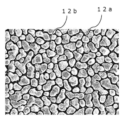
図1に、本発明の一実施形態による電磁波透過性金属光沢物品(以下、「金属光沢物品」という。)1の概略断面図を示し、図3に、本発明の一実施形態による金属光沢物品1の金属層の電子顕微鏡写真(SEM画像)を示す。また、図9に、本発明の一実施形態における島状構造の金属層12の断面の透過型電子顕微鏡写真(TEM画像)を示す。
<1. Basic configuration>
FIG. 1 shows a schematic cross-sectional view of an electromagnetic wave transmitting metallic luster article (hereinafter referred to as "metallic luster article") 1 according to one embodiment of the present invention, and FIG. 3 shows a metallic luster article according to one embodiment of the present invention. 1 shows an electron micrograph (SEM image) of the metal layer of No. 1. FIG. Further, FIG. 9 shows a transmission electron micrograph (TEM image) of a cross section of the
金属光沢物品1は、基体10と、基体10の上に形成された、金属層12と、を含む。また、金属層の基体側とは反対側の面上に形成されたバリア層13をさらに含む。
A
金属層12は基体10の上に形成される。金属層12は複数の部分12aを含む。金属層12におけるこれらの部分12aは、少なくとも一部において互いに不連続の状態、言い換えれば、少なくとも一部において隙間12bによって隔てられる。隙間12bによって隔てられるため、金属光沢物品のシート抵抗は大きくなり、電波との相互作用が低下するため、電波を透過させることができる。これらの各部分12aは金属を蒸着、スパッタ等することによって形成されたスパッタ粒子の集合体であってもよい。
A
尚、本明細書でいう「不連続の状態」とは、隙間12bによって互いに隔てられており、この結果、互いに電気的に絶縁されている状態を意味する。電気的に絶縁されることにより、金属光沢物品のシート抵抗が大きくなり、所望とする電磁波透過性が得られることになる。すなわち、不連続の状態で形成された金属層12によれば、十分な光輝性が得られやすく、電磁波透過性を確保することもできる。不連続の形態は、特に限定されるものではなく、例えば、島状構造、クラック構造等が含まれる。ここで「島状構造」とは、図3に示されているように、金属粒子同士が各々独立しており、それらの粒子が、互いに僅かに離間し又は一部接触した状態で敷き詰められてなる構造である。
The term "discontinuous state" as used in this specification means a state in which they are separated from each other by the
クラック構造とは、金属薄膜がクラックにより分断された構造である。
クラック構造の金属層12は、例えば基材フィルム上に金属薄膜層を設け、屈曲延伸して金属薄膜層にクラックを生じさせることにより形成することができる。この際、基材フィルムと金属薄膜層の間に伸縮性に乏しい、即ち延伸によりクラックを生成しやすい素材からなる脆性層を設けることにより、容易にクラック構造の金属層12を形成することができる。
A crack structure is a structure in which a metal thin film is divided by cracks.
The
上述のとおり金属層12が不連続となる態様は特に限定されないが、生産性の観点からは島状構造とすることが好ましい。
As described above, the mode in which the
金属光沢物品1の電磁波透過性は、例えば電波透過減衰量により評価することができる。金属光沢物品1において、実施例の欄に記載の方法で測定したセンチ波帯域(5GHz)における電波透過減衰量は、10[-dB]以下であることが好ましく、5[-dB]以下であるのがより好ましく、2[-dB]以下であることが更に好ましい。10[-dB]より大きいと、90%以上の電波が遮断されるという問題がある。なお、センチ波帯域(5GHz)における電波透過減衰量とミリ波レーダーの周波数帯域(76~80GHz)における電波透過減衰量との間には相関性があり、比較的近い値を示すことから、センチ波帯域における電磁波透過性に優れる金属光沢物品は、ミリ波レーダーの周波数帯域における電磁波透過性にも優れる。
The electromagnetic wave transmittance of the metallic
金属光沢物品1のシート抵抗も電磁波透過性と相関を有する。金属光沢物品1のシート抵抗は100Ω/□以上であるのが好ましく、この場合センチ波帯域(5GHz)における電波透過減衰量は、10~0.01[-dB]程度となる。金属光沢物品のシート抵抗は200Ω/□以上であることがより好ましく、600Ω/□以上であることが更に好ましい。また、特に好ましくは、1000Ω/□以上である。
金属光沢物品1のシート抵抗は、JIS-Z2316-1:2014に従って渦電流測定法により測定することができる。
The sheet resistance of the metallic
The sheet resistance of the metallic
金属光沢物品1の電波透過減衰量及びシート抵抗は、金属層12の材質や厚さ等により影響を受ける。また、金属光沢物品1が酸化インジウム含有層11を備える場合には酸化インジウム含有層11の材質や厚さ等によっても影響を受ける。
The radio wave transmission attenuation and sheet resistance of the metallic
<2.基体>
基体10としては、電磁波透過性の観点から、樹脂、ガラス、セラミックス等が挙げられる。
基体10は、基材フィルム、樹脂成型物基材、ガラス基材、又は金属光沢を付与すべき物品のいずれかであってもよい。
より具体的には、基材フィルムとしては、例えば、ポリエチレンテレフタレート(PET)、ポリエチレンナフタレート(PEN)、ポリブチレンテレフタレート、ポリアミド、ポリ塩化ビニル、ポリカーボネート(PC)、シクロオレフィンポリマー(COP)、ポリスチレン、ポリプロピレン(PP)、ポリエチレン、ポリシクロオレフィン、ポリウレタン、アクリル(PMMA)、ABSなどの単独重合体や共重合体からなる透明フィルムを用いることができる。
<2. Substrate>
Examples of the base 10 include resin, glass, and ceramics from the viewpoint of electromagnetic wave permeability.
The
More specifically, the base film includes, for example, polyethylene terephthalate (PET), polyethylene naphthalate (PEN), polybutylene terephthalate, polyamide, polyvinyl chloride, polycarbonate (PC), cycloolefin polymer (COP), polystyrene , polypropylene (PP), polyethylene, polycycloolefin, polyurethane, acrylic (PMMA), ABS, and other homopolymers or copolymers.
これらの部材によれば、光輝性や電磁波透過性に影響を与えることもない。但し、酸化インジウム含有層11や金属層12を後に形成する観点から、蒸着やスパッタ等の高温に耐え得るものであることが好ましく、従って、上記材料の中でも、例えば、ポリエチレンテレフタレート、ポリエチレンナフタレート、アクリル、ポリカーボネート、シクロオレフィンポリマー、ABS、ポリプロピレン、ポリウレタンが好ましい。なかでも、耐熱性とコストとのバランスがよいことからポリエチレンテレフタレートやシクロオレフィンポリマー、ポリカーボネート、アクリルが好ましい。
These members do not affect the brilliance or electromagnetic wave permeability. However, from the viewpoint of forming the indium oxide-containing
基材フィルムは、単層フィルムでもよいし積層フィルムでもよい。加工のし易さ等から、厚さは、例えば、6μm~250μm程度が好ましい。酸化インジウム含有層11や金属層12との付着力を強くするために、プラズマ処理や易接着処理などが施されてもよい。
基体10が基材フィルムの場合、金属層12は基材フィルム上の少なくとも一部に設ければよく、基材フィルムの片面のみに設けてもよく、両面に設けてもよい。
The base film may be a single layer film or a laminated film. The thickness is preferably, for example, about 6 μm to 250 μm from the viewpoint of ease of processing. In order to strengthen the adhesive force with the indium oxide-containing
When the
ここで、基材フィルムは、その表面上に金属層12を形成することができる対象(基体10)の一例にすぎない点に注意すべきである。基体10には、上記のとおり基材フィルムの他、樹脂成型物基材、ガラス基材、金属光沢を付与すべき物品それ自体も含まれる。樹脂成型物基材、及び金属光沢を付与すべき物品としては、例えば、車両用構造部品、車両搭載用品、電子機器の筐体、家電機器の筐体、構造用部品、機械部品、種々の自動車用部品、電子機器用部品、家具、台所用品等の家財向け用途、医療機器、建築資材の部品、その他の構造用部品や外装用部品等が挙げられる。
It should be noted here that the base film is only one example of an object (substrate 10) on which the
金属層12は、これら全ての基体上に形成することができ、基体の表面の一部に形成してもよく、基体の表面の全てに形成してもよい。この場合、金属層12を付与すべき基体10は、上記の基材フィルムと同様の材質、条件を満たしていることが好ましい。
The
<3.酸化インジウム含有層>
また、一実施形態に係る電磁波透過性金属光沢物品1は、図2に示されるように、基体10と金属層12の間に、酸化インジウム含有層11をさらに備えてもよい。酸化インジウム含有層11は、基体10の面に直接設けられていてもよいし、基体10の面に設けられた保護膜等を介して間接的に設けられてもよい。酸化インジウム含有層11は、金属光沢を付与すべき基体10の面に連続状態で、言い換えれば、隙間なく、設けられるのが好ましい。連続状態で設けられることにより、酸化インジウム含有層11、ひいては、金属層12や電磁波透過性金属光沢物品1の平滑性や耐食性を向上させることができ、また、酸化インジウム含有層11を面内ばらつきなく成膜することも容易となる。
<3. Indium oxide-containing layer>
In addition, the electromagnetic wave transmitting
このように、基体10と金属層12の間に、酸化インジウム含有層11をさらに備えること、すなわち、基体10の上に酸化インジウム含有層11を形成し、その上に金属層12を形成することによれば、金属層12を不連続の状態で形成しやすくなるため好ましい。そのメカニズムの詳細は必ずしも明らかではないが、金属の蒸着やスパッタによるスパッタ粒子が基体上で薄膜を形成する際には、基体上での粒子の表面拡散性が薄膜の形状に影響を及ぼし、基体の温度が高く、基体に対する金属層の濡れ性が小さく、金属層の材料の融点が低い方が不連続構造を形成しやすいと考えられる。そして、基体上に酸化インジウム含有層を設けることにより、その表面上の金属粒子の表面拡散性が促進されて、金属層を不連続の状態で成長させやすくなると考えられる。
Thus, further providing an indium oxide-containing
酸化インジウム含有層11として、酸化インジウム(In2O3)そのものを使用することもできるし、例えば、インジウム錫酸化物(ITO)や、インジウム亜鉛酸化物(IZO)のような金属含有物を使用することもできる。但し、第二の金属を含有したITOやIZOの方が、スパッタリング工程での放電安定性が高い点で、より好ましい。これらの酸化インジウム含有層11を用いることにより、基体の面に沿って連続状態の膜を形成することもでき、また、この場合には、酸化インジウム含有層の上に積層される金属層を、例えば、島状の不連続構造としやすくなるため、好ましい。更に、後述するように、この場合には、金属層に、クロム(Cr)又はインジウム(In)だけでなく、通常は不連続構造になり難く、本用途には適用が難しかった、アルミニウム等の様々な金属を含めやすくなる。
As the indium oxide-containing
ITOに含まれる酸化錫(SnО2)の質量比率である含有率(含有率=(SnO2/(In2O3+SnO2))×100)は特に限定されるものではないが、例えば、2.5wt%~30wt%、より好ましくは、3wt%~10wt%である。また、IZOに含まれる酸化亜鉛(ZnO)の質量比率である含有率(含有率=(ZnO/(In2O3+ZnO))×100)は、例えば、2wt%~20wt%である。酸化インジウム含有層11の厚さは、シート抵抗や電波透過減衰量、生産性の観点から、通常1000nm以下が好ましく、50nm以下がより好ましく、20nm以下が更に好ましい。一方、積層される金属層12を不連続状態としやすくするためには、1nm以上であることが好ましく、確実に不連続状態にしやすくするためには、2nm以上であることがより好ましく、5nm以上であることが更に好ましい。
The content ratio (content ratio = (SnO 2 /(In 2 O 3 +SnO 2 )) × 100), which is the mass ratio of tin oxide (SnO 2 ) contained in ITO, is not particularly limited. .5 wt% to 30 wt%, more preferably 3 wt% to 10 wt%. Also, the content rate (content rate=(ZnO/(In 2 O 3 +ZnO))×100), which is the mass ratio of zinc oxide (ZnO) contained in IZO, is, for example, 2 wt % to 20 wt %. The thickness of the indium oxide-containing
<4.金属層>
金属層12は、十分な光輝性を発揮し得ることは勿論、融点が比較的低いものであることが望ましい。金属層12は、スパッタリングを用いた薄膜成長によって形成するのが好ましいためである。このような理由から、金属層12としては、融点が約1000℃以下の金属が適しており、例えば、アルミニウム(Al)、亜鉛(Zn)、鉛(Pb)、銅(Cu)、銀(Ag)から選択された少なくとも一種の金属、および該金属を主成分とする合金のいずれかを含むことが好ましい。特に、物質の光輝性や安定性、価格等の理由からAlおよびそれらの合金が好ましい。また、アルミニウム合金を用いる場合には、アルミニウム含有量を50質量%以上とすることが好ましい。
<4. Metal layer>
It is desirable that the
金属層12の厚さは、十分な光輝性を発揮するように、通常10nm以上が好ましく、一方、シート抵抗や電波透過減衰量の観点から、通常100nm以下が好ましい。例えば、15nm~70nmが好ましく、15nm~50nmがより好ましい。この厚さは、均一な膜を生産性良く形成するのにも適しており、また、最終製品である樹脂成形品の見栄えも良い。なお、金属層12の厚さは例えば以下のようにして測定できる。
(金属層の厚さの測定方法)
まず、金属光沢物品から、図8に示すように一辺5cmの正方形領域3を適当に抽出し、該正方形領域3の縦辺及び横辺それぞれの中心線A、Bをそれぞれ4等分することによって得られる計5箇所の点「a」~「e」を測定箇所として選択する。
次いで、選択した測定箇所それぞれにおける、図9に示すような断面画像(透過型電子顕微鏡写真(TEM画像))を測定し、得られたTEM画像から、5個以上の金属部分12aが含まれる視野角領域を抽出する。
5箇所の測定箇所それぞれにおいて抽出された視野角領域における金属層の総断面積を視野角領域の横幅で割ったものを各視野角領域の金属層の厚さとし、5箇所の測定箇所それぞれにおける、各視野角領域の金属層の厚さの平均値を金属層の厚さとする。
The thickness of the
(Method for measuring thickness of metal layer)
First, as shown in FIG. 8, a
Next, a cross-sectional image (transmission electron micrograph (TEM image)) as shown in FIG. 9 is measured at each of the selected measurement points, and from the obtained TEM image, a field of view containing five or
The thickness of the metal layer in each viewing angle region is obtained by dividing the total cross-sectional area of the metal layer in the viewing angle region extracted at each of the five measurement locations by the width of the viewing angle region, and at each of the five measurement locations, Let the average value of the thickness of the metal layer in each viewing angle region be the thickness of the metal layer.
また、同様の理由から、金属層12の厚さと酸化インジウム含有層11の厚さとの比(金属層12の厚さ/酸化インジウム含有層11の厚さ)は、0.1~100の範囲が好ましく、0.3~35の範囲がより好ましい。
Also, for the same reason, the ratio of the thickness of the
金属層12の部分12aの円相当径は特に限定されないが、通常10~1000nm程度である。また、各部分12a同士の距離は特に限定されないが、通常は10~1000nm程度である。
The equivalent circle diameter of the
<5.バリア層>
金属光沢物品1は、図1及び2に示すように、金属層12の基体10側とは反対側の面上にバリア層13を備える。なお、バリア層13は金属層12上に積層されていればよく、必ずしも隙間12bを完全に埋めていなくてもよい。
バリア層は、金属層12の酸化(腐食)を抑制するための層である。バリア層は、金属および半金属の少なくとも1種の酸化物、窒化物、炭化物、酸化窒化物、酸化炭化物、窒化炭化物および酸化窒化炭化物からなる群より選ばれる少なくとも1種を含む。金属としては、例えば、アルミニウム、チタン、インジウム、マグネシウムなどを用いることができ、半金属としては、例えば、ケイ素、ビスマス、ゲルマニウムなどを用いることができる。
具体的には、例えばZnO+Al2O3(AZO)、酸化インジウム亜鉛(IZO)、酸化インジウム錫(ITO)、酸化炭化窒化ケイ素膜(SiOCN)、酸化窒化ケイ素膜(SiON)、窒化ケイ素膜(SiN)、SiOX、AlOX、AlON、TiOX等を用いることができる。中でも、AZO、ITO、AlOX及びSiO2からなる群より選ばれる少なくとも一種を用いることが好ましい。
バリア層が金属層12の酸化(腐食)を抑制する性能(以下「バリア性」ともいう)の向上のためには、バリア層内におけるネットワーク構造(網目状の構造)を緻密にするような炭素、窒素を含むことが好ましい。さらに透明性を向上させるためには、酸素を含有していることが好ましい。すなわち、バリア層は、金属および半金属の少なくとも1種の酸化窒化炭化物を含むことが好ましい。
<5. Barrier layer>
The
The barrier layer is a layer for suppressing oxidation (corrosion) of the
Specifically, for example, ZnO+Al 2 O 3 (AZO), indium zinc oxide (IZO), indium tin oxide (ITO), silicon oxycarbonitride film (SiOCN), silicon oxynitride film (SiON), silicon nitride film (SiN ), SiO x , AlO x , AlON, TiO x and the like can be used. Among them, it is preferable to use at least one selected from the group consisting of AZO, ITO, AlO X and SiO 2 .
In order to improve the performance of the barrier layer to suppress the oxidation (corrosion) of the metal layer 12 (hereinafter also referred to as “barrier property”), carbon atoms that make the network structure (mesh-like structure) in the barrier layer dense. , preferably containing nitrogen. In order to further improve transparency, it is preferable to contain oxygen. That is, the barrier layer preferably contains at least one carbide oxynitride of a metal and a metalloid.
また、バリア性の向上のためには、バリア層は水蒸気を透過しにくいことが好ましい。バリア層の水蒸気の透過の度合いは種々の方法により評価できるが、例えば実施例の欄に記載の方法により測定した水蒸気透過量を用いて評価することができる。バリア性の向上のためには、当該水蒸気透過量が5g/m2・day以下であることが好ましく、3g/m2・day以下であることがより好ましく、2g/m2・day以下であることが更に好ましい。 Moreover, in order to improve barrier properties, it is preferable that the barrier layer is difficult to permeate water vapor. The degree of water vapor permeation of the barrier layer can be evaluated by various methods. In order to improve barrier properties, the water vapor permeation amount is preferably 5 g/m 2 ·day or less, more preferably 3 g/m 2 ·day or less, and 2 g/m 2 ·day or less. is more preferred.
バリア層13の厚みは特に限定はされないが、バリア性を向上させるためには1nm以上が好ましく、5nm以上がより好ましく、10nm以上が更に好ましい。また、電磁波透過性や外観の金属光沢感を向上させるためには100nm以下が好ましく、80nm以下がより好ましく、60nm以下が更に好ましい。
Although the thickness of the
また、金属層12の酸化(腐食)をより一層抑制するために、バリア層は図4~7に示すように、金属層と基体との間にさらに設けられてもよい。
金属光沢物品1が酸化インジウム含有層を備える場合は、図5に示すように酸化インジウム含有層と金属層の間にバリア層を設けてもよく、図6に示すように酸化インジウム含有層の金属層とは反対側にバリア層を設けてもよい。また、図7に示すようにこの両方に設けてもよい。
In order to further suppress oxidation (corrosion) of the
When the article with
また、金属光沢物品は、上述の金属層、酸化インジウム含有層、及びバリア層の他に、用途に応じてその他の層を備えてもよい。
その他の層としては色味等の外観を調整するための高屈折材料等の光学調整層(色味調整層)、耐擦傷性等の耐久性を向上させるための保護層(耐擦傷性層)、易接着層、ハードコート層、反射防止層、光取出し層、アンチグレア層等が挙げられる。
In addition to the metal layer, the indium oxide-containing layer, and the barrier layer described above, the article with metallic luster may include other layers depending on the application.
Other layers include an optical adjustment layer (color adjustment layer) such as a high refractive material for adjusting appearance such as color, and a protective layer (scratch resistant layer) for improving durability such as scratch resistance. , an easy adhesion layer, a hard coat layer, an antireflection layer, a light extraction layer, an antiglare layer, and the like.
<6.金属光沢物品の製造>
金属光沢物品1の製造方法の一例について、説明する。特に説明しないが、基材フィルム10以外の基体を用いた場合についても同様の方法で製造することができる。
<6. Production of metallic luster article>
An example of the method for manufacturing the article with
基体10上に金属層12を形成するにあたっては、例えば、真空蒸着、スパッタリング等の方法を用いることができる。
For forming the
また、基体10上に酸化インジウム含有層11を形成する場合には、金属層12の形成に先立ち、酸化インジウム含有層11を、真空蒸着、スパッタリング、イオンプレーティング等によって形成する。但し、大面積でも厚さを厳密に制御できる点から、スパッタリングが好ましい。
When the indium oxide-containing
バリア層は、蒸着、スパッタリング、化学気相堆積法(CVD)のような真空を用いたドライプロセスにより形成される。これにより、非常に緻密でバリア性の高いバリア層を得ることができる。この中でも、蒸着法が好ましい。蒸着法は、成膜速度が非常に速いプロセスであり、生産性の高いプロセスであるため、生産効率が良いためである。特に好ましいのは、アーク放電プラズマを利用した蒸着法を用いて形成することである。アーク放電プラズマは、通常使用されるグロー放電プラズマとは異なり、非常に高い電子密度であることがわかっている。蒸着法にアーク放電プラズマを用いることで、反応性を高くすることができ、非常に緻密なバリア層が形成できる。 The barrier layer is formed by a vacuum dry process such as evaporation, sputtering, or chemical vapor deposition (CVD). This makes it possible to obtain a very dense barrier layer with high barrier properties. Among these, the vapor deposition method is preferable. This is because the vapor deposition method is a process with a very high film formation speed and a high productivity process, so that the production efficiency is good. Particularly preferred is formation using a vapor deposition method utilizing arc discharge plasma. Arc discharge plasmas have been found to have very high electron densities, unlike the commonly used glow discharge plasmas. By using arc discharge plasma in the vapor deposition method, reactivity can be increased and a very dense barrier layer can be formed.
アーク放電プラズマは、例えば、圧力勾配型プラズマガン、直流放電プラズマ発生装置、高周波放電プラズマ発生装置などで形成可能であるが、中でも蒸着中でも安定して高密度なプラズマを発生することが可能な圧力勾配型プラズマガンを用いることが好ましい。 Arc discharge plasma can be formed by, for example, a pressure gradient plasma gun, a DC discharge plasma generator, a high frequency discharge plasma generator, etc. Among them, the pressure that can stably generate high-density plasma even during deposition is Preferably, a gradient plasma gun is used.
尚、基体10と金属層12の間に酸化インジウム含有層11を設ける場合、酸化インジウム含有層11と金属層12の間には、バリア層13等の他の層を介在させずに直接接触させるのが好ましい。
When the indium oxide-containing
<7.金属光沢物品及び金属薄膜の用途>
本実施形態の金属光沢物品1及び金属薄膜は、電磁波透過性を有することから電磁波を送受信する装置や物品及びその部品等に使用することが好ましい。例えば、車両用構造部品、車両搭載用品、電子機器の筐体、家電機器の筐体、構造用部品、機械部品、種々の自動車用部品、電子機器用部品、家具、台所用品等の家財向け用途、医療機器、建築資材の部品、その他の構造用部品や外装用部品等が挙げられる。
より具体的には、車両関係では、インスツルメントパネル、コンソールボックス、ドアノブ、ドアトリム、シフトレバー、ペダル類、グローブボックス、バンパー、ボンネット、フェンダー、トランク、ドア、ルーフ、ピラー、座席シート、ステアリングホイール、ECUボックス、電装部品、エンジン周辺部品、駆動系・ギア周辺部品、吸気・排気系部品、冷却系部品等が挙げられる。
電子機器および家電機器としてより具体的には、冷蔵庫、洗濯機、掃除機、電子レンジ、エアコン、照明機器、電気湯沸かし器、テレビ、時計、換気扇、プロジェクター、スピーカー等の家電製品類、パソコン、携帯電話、スマートフォン、デジタルカメラ、タブレット型PC、携帯音楽プレーヤー、携帯ゲーム機、充電器、電池等電子情報機器等が挙げられる。
<7. Uses of Metallic Lustrous Articles and Metal Thin Films>
Since the metallic
More specifically, for vehicles, instrument panels, console boxes, door knobs, door trims, shift levers, pedals, glove boxes, bumpers, bonnets, fenders, trunks, doors, roofs, pillars, seats, steering wheels , ECU boxes, electrical components, engine peripheral parts, drive system/gear peripheral parts, intake/exhaust system parts, cooling system parts, and the like.
More specifically, as electronic equipment and home appliances, refrigerators, washing machines, vacuum cleaners, microwave ovens, air conditioners, lighting equipment, electric water heaters, televisions, clocks, ventilation fans, projectors, speakers, personal computers, mobile phones, etc. , smart phones, digital cameras, tablet PCs, portable music players, portable game machines, battery chargers, electronic information devices such as batteries, and the like.
以下、実施例及び比較例を挙げて、本発明をより具体的に説明する。実施例1~10及び比較例1の金属光沢物品を準備し、バリア層の水蒸気透過量、電波透過減衰量(-dB)、シート抵抗、20°光沢度、反射率を測定した。なお、基体10としては、基材フィルムを用いた。
評価方法の詳細は以下のとおりである。
EXAMPLES Hereinafter, the present invention will be described more specifically with reference to examples and comparative examples. Metallic glossy articles of Examples 1 to 10 and Comparative Example 1 were prepared, and the water vapor permeation amount, radio wave transmission attenuation (-dB), sheet resistance, 20° glossiness, and reflectance of the barrier layer were measured. A substrate film was used as the
The details of the evaluation method are as follows.
(1)バリア層の水蒸気透過量
MOCON社製水蒸気透過度測定装置PERMATRAN-W Model3/33を用いて、40℃90%RH環境下におけるバリア膜単膜の水蒸気透過度を評価した。
(1) Amount of Water Vapor Permeation of Barrier Layer Using a water vapor permeability measuring device PERMATRAN-
(2)電波透過減衰量
5GHzにおける電波透過減衰量を導波管法測定評価治具およびベクトルネットワークアナライザMS4644B(アンリツ株式会社)を用いて評価した。
(2) Radio Wave Transmission Attenuation The radio wave transmission attenuation at 5 GHz was evaluated using a waveguide method measurement evaluation jig and a vector network analyzer MS4644B (Anritsu Corporation).
(3)シート抵抗
ナプソン社製非接触式抵抗測定装置NC-80MAP(測定上限:3000Ω/□)を用い、JIS-Z2316に準拠し、渦電流測定法により金属層と酸化インジウム含有層の積層体としてのシート抵抗を測定した。
(3) Sheet resistance Using a non-contact resistance measuring device NC-80MAP (measurement upper limit: 3000 Ω / □) manufactured by Napson, in accordance with JIS-Z2316, a laminate of a metal layer and an indium oxide-containing layer is measured by an eddy current measurement method. The sheet resistance was measured as
(4)20°光沢度
金属光沢物品の20°光沢度をJIS Z 8741(1997年版)に準拠して測定した。具体的には、PG-IIM(20°グロス測定、日本電色工業株式会社製)を用いて測定を行った。なお、20°光沢度の測定は金属層側の面に対して行った。
この20°光沢度は、900以上であることが好ましく、1100以上であることがより好ましく、1300以上であることが特に好ましい。900より小さいと、光輝性に劣り金属外観が得られないという問題がある。
(4) 20° Glossiness The 20° glossiness of the article with metallic luster was measured according to JIS Z 8741 (1997 edition). Specifically, the measurement was performed using PG-IIM (20° gloss measurement, manufactured by Nippon Denshoku Industries Co., Ltd.). The 20° glossiness was measured on the surface facing the metal layer.
The 20° glossiness is preferably 900 or more, more preferably 1100 or more, and particularly preferably 1300 or more. If it is less than 900, there is a problem that the luster is inferior and a metallic appearance cannot be obtained.
(5)反射率
日立分光光度計U-4100を用いて、波長550nmにおける0°反射率を測定した。
次いで、金属光沢物品を60℃、95%RHの条件下に放置し、250時間後、及び500時間後に、同様にして反射率を測定した。
また、500時間後の反射率の、初期の反射率に対する割合(500時間後反射率維持率)を求めた。
(5) Reflectance 0° reflectance at a wavelength of 550 nm was measured using a Hitachi spectrophotometer U-4100.
Then, the article with metallic luster was left under conditions of 60° C. and 95% RH, and the reflectance was similarly measured after 250 hours and 500 hours.
Also, the ratio of the reflectance after 500 hours to the initial reflectance (reflectance retention rate after 500 hours) was determined.
[比較例1]
基材フィルムとして、三菱樹脂社製PETフィルム(厚さ125μm、340mm幅)を用いた。
先ず、DCマグネトロンスパッタリングを用いて、基材フィルムの面に沿って、5nmの厚さのITO層をその上に直接形成した。ITO層を形成する際の基材フィルムの温度は、130℃に設定した。ITOに含まれる酸化錫(SnО2)の含有率(含有率=(SnO2/(In2O3+SnO2))×100)は10wt%である。
[Comparative Example 1]
A PET film (thickness: 125 µm, width: 340 mm) manufactured by Mitsubishi Plastics, Inc. was used as the base film.
First, a 5 nm thick ITO layer was directly formed on the substrate film along the surface thereof using DC magnetron sputtering. The temperature of the base film when forming the ITO layer was set to 130°C. The content of tin oxide (SnO 2 ) contained in ITO (content=(SnO 2 /(In 2 O 3 +SnO 2 ))×100) is 10 wt %.
次いで、交流スパッタリング(AC:40kHz)を用いて、ITO層の上に厚さ30nmのアルミニウム(Al)層を形成し、バリア層を備えない金属光沢物品を得た。なお、得られたアルミニウム層は不連続層であった。Al層を形成する際の基材フィルムの温度は、130℃に設定した。 Then, alternating current sputtering (AC: 40 kHz) was used to form a 30 nm thick aluminum (Al) layer on the ITO layer to obtain a metallic luster article without a barrier layer. The obtained aluminum layer was a discontinuous layer. The temperature of the substrate film when forming the Al layer was set to 130°C.
[実施例1~4]
比較例1と同様にして得られたバリア層を備えない金属光沢物品のアルミニウム層上に、DCマグネトロンスパッタリングを用いて、種々の厚みのAZOからなるバリア層を形成し、実施例1~4の金属光沢物品を得た。バリア層を形成する際の基材フィルムの温度は、130℃に設定した。なお、AZOは三菱マテリアル製AZO-low nを使用した。なお、バリア層の厚みは先述の金属層の厚みの測定方法と同様の方法で測定した。
[Examples 1 to 4]
Barrier layers of various thicknesses made of AZO were formed by DC magnetron sputtering on the aluminum layer of the metallic luster article without a barrier layer obtained in the same manner as in Comparative Example 1. An article with metallic luster was obtained. The temperature of the base film when forming the barrier layer was set to 130°C. AZO used was AZO-low n manufactured by Mitsubishi Materials. The thickness of the barrier layer was measured by the same method as the method for measuring the thickness of the metal layer.
[実施例5]
ITOからなるバリア層を形成した以外は、実施例2と同様にして実施例5の金属光沢物品を得た。なお、ITOに含まれる酸化錫(SnО2)の含有率(含有率=(SnO2/(In2O3+SnO2))×100)は30wt%であった。
[Example 5]
An article with metallic luster of Example 5 was obtained in the same manner as in Example 2, except that a barrier layer made of ITO was formed. The content of tin oxide (SnO 2 ) contained in ITO (content=(SnO 2 /(In 2 O 3 +SnO 2 ))×100) was 30 wt %.
[実施例6、7]
比較例1と同様にして得られたバリア層を備えない金属光沢物品のアルミニウム層上に、RF(13.6MHz)電源スパッタリングを用いて、種々の厚みのAlOxからなるバリア層を形成し、実施例6、7の金属光沢物品を得た。バリア層を形成する際の基材フィルムの温度は、室温に設定した。
[Examples 6 and 7]
RF (13.6 MHz) power supply sputtering was used to form a barrier layer of AlO x with various thicknesses on the aluminum layer of the metallic luster article without a barrier layer obtained in the same manner as in Comparative Example 1, Metallic luster articles of Examples 6 and 7 were obtained. The temperature of the base film when forming the barrier layer was set to room temperature.
[実施例8~10]
比較例1と同様にして得られたバリア層を備えない金属光沢物品のアルミニウム層上に、RF(13.6MHz)電源スパッタリングを用いて、種々の厚みのSiO2からなるバリア層を形成し、実施例8~10の金属光沢物品を得た。バリア層を形成する際の基材フィルムの温度は、室温に設定した。
[Examples 8 to 10]
RF (13.6 MHz) power supply sputtering was used to form a barrier layer made of SiO2 of various thicknesses on the aluminum layer of the metallic luster article without a barrier layer obtained in the same manner as in Comparative Example 1, Metallic luster articles of Examples 8-10 were obtained. The temperature of the base film when forming the barrier layer was set to room temperature.
以下の表1に、結果を示す。 The results are shown in Table 1 below.

実施例1~10の金属光沢物品は、いずれもバリア層を備えない比較例1の金属光沢物品と比較すると、500時間後反射率維持率が高かった。すなわち、実施例1~10の金属光沢物品は、いずれもバリア層を備えない比較例1の金属光沢物品と比較するとアルミニウム層の酸化(腐食)を抑制することができた。 The articles with metallic luster of Examples 1 to 10 all had higher reflectance retention after 500 hours than the article with metallic luster of Comparative Example 1, which did not have a barrier layer. That is, the metallic lustrous articles of Examples 1 to 10 were able to suppress the oxidation (corrosion) of the aluminum layer as compared with the metallic lustrous article of Comparative Example 1, which did not have a barrier layer.
なお、以上の実施例で特に使用したアルミニウム(Al)以外の金属についても、亜鉛(Zn)、鉛(Pb)、銅(Cu)、銀(Ag)などの比較的融点の低い金属については、同様の手法で不連続構造を形成しうると考えられる。 As for metals other than aluminum (Al) used in the above examples, metals with relatively low melting points such as zinc (Zn), lead (Pb), copper (Cu), and silver (Ag) It is believed that a discontinuous structure can be formed in a similar manner.
本発明は前記実施例に限定されるものではなく、発明の趣旨から逸脱しない範囲で適宜変更して具体化することもできる。 The present invention is not limited to the above-described embodiments, and can be embodied with appropriate modifications without departing from the gist of the invention.
本発明に係る金属光沢物品は、電磁波を送受信する装置や物品及びその部品等に使用することができる。例えば、車両用構造部品、車両搭載用品、電子機器の筐体、家電機器の筐体、構造用部品、機械部品、種々の自動車用部品、電子機器用部品、家具、台所用品等の家財向け用途、医療機器、建築資材の部品、その他の構造用部品や外装用部品等、意匠性と電磁波透過性の双方が要求される様々な用途にも利用できる。 INDUSTRIAL APPLICABILITY The metallic luster article according to the present invention can be used for devices, articles, and parts thereof that transmit and receive electromagnetic waves. For example, structural parts for vehicles, articles mounted on vehicles, housings for electronic devices, housings for home appliances, structural parts, machine parts, various automobile parts, electronic device parts, furniture, household goods such as kitchen utensils , medical equipment, building material parts, other structural parts and exterior parts, etc., where both good design and electromagnetic wave permeability are required.
1 金属光沢物品
10 基体
11 酸化インジウム含有層
12 金属層
12a 部分
12b 隙間
13 バリア層
Claims (13)
前記金属層は、少なくとも一部において互いに不連続の状態にある複数の部分を含み、
前記金属層の厚さは、20nmより大きく100nm以下である、電磁波透過性金属光沢物品。 a base, a metal layer formed on the base, and a barrier layer formed on a surface of the metal layer opposite to the base,
The metal layer includes a plurality of portions that are discontinuous at least in part,
The electromagnetic wave transmitting metallic luster article , wherein the thickness of the metal layer is greater than 20 nm and less than or equal to 100 nm .
Priority Applications (3)
| Application Number | Priority Date | Filing Date | Title |
|---|---|---|---|
| PCT/JP2019/017003 WO2019208489A1 (en) | 2018-04-23 | 2019-04-22 | Electromagnetic wave-transmitting metallic-luster article |
| KR1020207029951A KR20210005586A (en) | 2018-04-23 | 2019-04-22 | Electromagnetically transparent metallic polished articles |
| TW108114182A TW201943872A (en) | 2018-04-23 | 2019-04-23 | Electromagnetic wave-transmitting metallic-luster article |
Applications Claiming Priority (2)
| Application Number | Priority Date | Filing Date | Title |
|---|---|---|---|
| JP2018082662 | 2018-04-23 | ||
| JP2018082662 | 2018-04-23 |
Publications (2)
| Publication Number | Publication Date |
|---|---|
| JP2019188805A JP2019188805A (en) | 2019-10-31 |
| JP7319078B2 true JP7319078B2 (en) | 2023-08-01 |
Family
ID=68388900
Family Applications (1)
| Application Number | Title | Priority Date | Filing Date |
|---|---|---|---|
| JP2019080623A Active JP7319078B2 (en) | 2018-04-23 | 2019-04-22 | Electromagnetic wave permeable metallic luster article |
Country Status (4)
| Country | Link |
|---|---|
| JP (1) | JP7319078B2 (en) |
| KR (1) | KR20210005586A (en) |
| CN (1) | CN112020424A (en) |
| TW (1) | TW201943872A (en) |
Families Citing this family (1)
| Publication number | Priority date | Publication date | Assignee | Title |
|---|---|---|---|---|
| WO2022181528A1 (en) * | 2021-02-24 | 2022-09-01 | 日東電工株式会社 | Electromagnetically permeable member with metallic gloss, and decorative member |
Citations (3)
| Publication number | Priority date | Publication date | Assignee | Title |
|---|---|---|---|---|
| JP2008221557A (en) | 2007-03-12 | 2008-09-25 | Ulvac Japan Ltd | Sheeny coat and manufacturing method of sheeny coat |
| WO2014097943A1 (en) | 2012-12-18 | 2014-06-26 | 東レ株式会社 | Metal dot substrate and method for manufacturing metal dot substrate |
| WO2018079547A1 (en) | 2016-10-24 | 2018-05-03 | 日東電工株式会社 | Electromagnetic wave-permeable shiny metal member, article using same, and metal thin film |
Family Cites Families (5)
| Publication number | Priority date | Publication date | Assignee | Title |
|---|---|---|---|---|
| JPH066783B2 (en) * | 1986-12-22 | 1994-01-26 | 株式会社麗光 | Deposition film for packaging |
| JP4706596B2 (en) | 2005-10-31 | 2011-06-22 | 豊田合成株式会社 | Resin product, method for producing the same, and method for forming metal film |
| CN101802248B (en) * | 2007-09-18 | 2013-10-16 | 信越聚合物株式会社 | Radio-wave-transmitting decorative member |
| JP2009298006A (en) | 2008-06-12 | 2009-12-24 | Toyoda Gosei Co Ltd | Electromagnetic wave permeable glittering resin product and manufacturing method |
| JP2010005999A (en) | 2008-06-30 | 2010-01-14 | Nissha Printing Co Ltd | Method of manufacturing metal film decorative sheet which has crack |
-
2019
- 2019-04-22 JP JP2019080623A patent/JP7319078B2/en active Active
- 2019-04-22 KR KR1020207029951A patent/KR20210005586A/en unknown
- 2019-04-22 CN CN201980027678.XA patent/CN112020424A/en active Pending
- 2019-04-23 TW TW108114182A patent/TW201943872A/en unknown
Patent Citations (3)
| Publication number | Priority date | Publication date | Assignee | Title |
|---|---|---|---|---|
| JP2008221557A (en) | 2007-03-12 | 2008-09-25 | Ulvac Japan Ltd | Sheeny coat and manufacturing method of sheeny coat |
| WO2014097943A1 (en) | 2012-12-18 | 2014-06-26 | 東レ株式会社 | Metal dot substrate and method for manufacturing metal dot substrate |
| WO2018079547A1 (en) | 2016-10-24 | 2018-05-03 | 日東電工株式会社 | Electromagnetic wave-permeable shiny metal member, article using same, and metal thin film |
Also Published As
| Publication number | Publication date |
|---|---|
| CN112020424A (en) | 2020-12-01 |
| JP2019188805A (en) | 2019-10-31 |
| KR20210005586A (en) | 2021-01-14 |
| TW201943872A (en) | 2019-11-16 |
Similar Documents
| Publication | Publication Date | Title |
|---|---|---|
| US11383478B2 (en) | Metallic lustrous member with electromagnetic wave transmissibility, article using the member, and metal thin film | |
| JP7319079B2 (en) | Electromagnetic wave permeable metallic luster article and decorative member | |
| JP7319077B2 (en) | Electromagnetic wave transparent metallic luster article and metal thin film | |
| WO2019208499A1 (en) | Electromagnetically permeable article with metallic gloss | |
| WO2019208493A1 (en) | Electromagnetic-wave-permeable metallic-luster article, and decorative member | |
| WO2021182380A1 (en) | Electromagnetic-wave-transmissive laminated member and method for manufacturing same | |
| JP7319078B2 (en) | Electromagnetic wave permeable metallic luster article | |
| JP2018192808A (en) | Electromagnetic wave transmissive metallic sheen member, article using the same and thin metallic film | |
| WO2019208504A1 (en) | Electromagnetic wave transparent metallic luster article, and metal thin film | |
| JP2019188809A (en) | Electromagnetic wave transmissible metallic sheen article | |
| JP7319080B2 (en) | Electromagnetic wave transparent metallic luster article and metal thin film | |
| JP7319081B2 (en) | Electromagnetic wave permeable metallic luster article | |
| WO2019208494A1 (en) | Electromagnetic wave transmissive metallic luster product and metal thin film | |
| WO2019208489A1 (en) | Electromagnetic wave-transmitting metallic-luster article | |
| WO2019208490A1 (en) | Electromagnetic wave-permeable metal glossy article and method for manufacturing same | |
| WO2022181528A1 (en) | Electromagnetically permeable member with metallic gloss, and decorative member | |
| WO2019208488A1 (en) | Electromagnetic wave transmissive metal luster article | |
| JP2023013743A (en) | Laminate and decorative member | |
| JP2022171450A (en) | Electromagnetically permeable member with metallic gloss, and decorative member | |
| JP2022129029A (en) | Electromagnetic wave transmissive metallic sheen member and decorative member |
Legal Events
| Date | Code | Title | Description |
|---|---|---|---|
| A621 | Written request for application examination |
Free format text: JAPANESE INTERMEDIATE CODE: A621 Effective date: 20220204 |
|
| A131 | Notification of reasons for refusal |
Free format text: JAPANESE INTERMEDIATE CODE: A131 Effective date: 20230214 |
|
| A521 | Request for written amendment filed |
Free format text: JAPANESE INTERMEDIATE CODE: A523 Effective date: 20230412 |
|
| TRDD | Decision of grant or rejection written | ||
| A01 | Written decision to grant a patent or to grant a registration (utility model) |
Free format text: JAPANESE INTERMEDIATE CODE: A01 Effective date: 20230620 |
|
| A61 | First payment of annual fees (during grant procedure) |
Free format text: JAPANESE INTERMEDIATE CODE: A61 Effective date: 20230720 |
|
| R150 | Certificate of patent or registration of utility model |
Ref document number: 7319078 Country of ref document: JP Free format text: JAPANESE INTERMEDIATE CODE: R150 |