KR20210007908A - Organic compound, light-emitting device, light-receiving device, light-emitting apparatus, light-emitting module, electronic device, and lighting device - Google Patents
Organic compound, light-emitting device, light-receiving device, light-emitting apparatus, light-emitting module, electronic device, and lighting device Download PDFInfo
- Publication number
- KR20210007908A KR20210007908A KR1020200085353A KR20200085353A KR20210007908A KR 20210007908 A KR20210007908 A KR 20210007908A KR 1020200085353 A KR1020200085353 A KR 1020200085353A KR 20200085353 A KR20200085353 A KR 20200085353A KR 20210007908 A KR20210007908 A KR 20210007908A
- Authority
- KR
- South Korea
- Prior art keywords
- light
- light emitting
- layer
- emitting device
- abbreviation
- Prior art date
Links
- 150000002894 organic compounds Chemical class 0.000 title claims abstract description 127
- 125000003118 aryl group Chemical group 0.000 claims abstract description 14
- 239000000758 substrate Substances 0.000 claims description 78
- 230000005525 hole transport Effects 0.000 claims description 64
- 238000000034 method Methods 0.000 claims description 44
- 125000004432 carbon atom Chemical group C* 0.000 claims description 35
- 125000001997 phenyl group Chemical group [H]C1=C([H])C([H])=C(*)C([H])=C1[H] 0.000 claims description 35
- 125000000217 alkyl group Chemical group 0.000 claims description 18
- 239000001257 hydrogen Substances 0.000 claims description 18
- 229910052739 hydrogen Inorganic materials 0.000 claims description 18
- 125000000753 cycloalkyl group Chemical group 0.000 claims description 9
- 125000002496 methyl group Chemical group [H]C([H])([H])* 0.000 claims description 8
- 125000000999 tert-butyl group Chemical group [H]C([H])([H])C(*)(C([H])([H])[H])C([H])([H])[H] 0.000 claims description 5
- 125000001624 naphthyl group Chemical group 0.000 claims description 4
- ICPSWZFVWAPUKF-UHFFFAOYSA-N 1,1'-spirobi[fluorene] Chemical group C1=CC=C2C=C3C4(C=5C(C6=CC=CC=C6C=5)=CC=C4)C=CC=C3C2=C1 ICPSWZFVWAPUKF-UHFFFAOYSA-N 0.000 claims description 3
- 125000004435 hydrogen atom Chemical class [H]* 0.000 claims 4
- 239000000126 substance Substances 0.000 abstract description 19
- 125000005913 (C3-C6) cycloalkyl group Chemical group 0.000 abstract description 2
- 125000004169 (C1-C6) alkyl group Chemical group 0.000 abstract 1
- 239000010410 layer Substances 0.000 description 427
- 239000000463 material Substances 0.000 description 234
- 238000005401 electroluminescence Methods 0.000 description 100
- 239000010408 film Substances 0.000 description 99
- YXFVVABEGXRONW-UHFFFAOYSA-N Toluene Chemical compound CC1=CC=CC=C1 YXFVVABEGXRONW-UHFFFAOYSA-N 0.000 description 59
- 238000002347 injection Methods 0.000 description 53
- 239000007924 injection Substances 0.000 description 53
- -1 aromatic amine compound Chemical class 0.000 description 51
- 230000015572 biosynthetic process Effects 0.000 description 46
- 238000005259 measurement Methods 0.000 description 40
- 238000003786 synthesis reaction Methods 0.000 description 39
- 230000032258 transport Effects 0.000 description 39
- 150000001875 compounds Chemical class 0.000 description 38
- 238000006243 chemical reaction Methods 0.000 description 35
- 230000006870 function Effects 0.000 description 32
- MILUBEOXRNEUHS-UHFFFAOYSA-N iridium(3+) Chemical compound [Ir+3] MILUBEOXRNEUHS-UHFFFAOYSA-N 0.000 description 30
- 239000007787 solid Substances 0.000 description 30
- IJGRMHOSHXDMSA-UHFFFAOYSA-N nitrogen Substances N#N IJGRMHOSHXDMSA-UHFFFAOYSA-N 0.000 description 29
- 229910052757 nitrogen Inorganic materials 0.000 description 27
- 239000004065 semiconductor Substances 0.000 description 26
- 230000003287 optical effect Effects 0.000 description 24
- KDLHZDBZIXYQEI-UHFFFAOYSA-N Palladium Chemical compound [Pd] KDLHZDBZIXYQEI-UHFFFAOYSA-N 0.000 description 23
- 230000000052 comparative effect Effects 0.000 description 23
- 229920005989 resin Polymers 0.000 description 23
- 239000011347 resin Substances 0.000 description 23
- 238000010586 diagram Methods 0.000 description 22
- 238000000295 emission spectrum Methods 0.000 description 22
- 229910052736 halogen Inorganic materials 0.000 description 22
- 150000002367 halogens Chemical class 0.000 description 22
- CUJRVFIICFDLGR-UHFFFAOYSA-N acetylacetonate Chemical compound CC(=O)[CH-]C(C)=O CUJRVFIICFDLGR-UHFFFAOYSA-N 0.000 description 20
- 238000000859 sublimation Methods 0.000 description 20
- 230000008022 sublimation Effects 0.000 description 20
- 239000007983 Tris buffer Substances 0.000 description 19
- ZUOUZKKEUPVFJK-UHFFFAOYSA-N diphenyl Chemical group C1=CC=CC=C1C1=CC=CC=C1 ZUOUZKKEUPVFJK-UHFFFAOYSA-N 0.000 description 19
- 239000011701 zinc Substances 0.000 description 19
- 239000010949 copper Substances 0.000 description 17
- 238000005859 coupling reaction Methods 0.000 description 17
- RYGMFSIKBFXOCR-UHFFFAOYSA-N Copper Chemical compound [Cu] RYGMFSIKBFXOCR-UHFFFAOYSA-N 0.000 description 16
- 229910052802 copper Inorganic materials 0.000 description 16
- WKBOTKDWSSQWDR-UHFFFAOYSA-N Bromine atom Chemical compound [Br] WKBOTKDWSSQWDR-UHFFFAOYSA-N 0.000 description 15
- 230000004888 barrier function Effects 0.000 description 15
- GDTBXPJZTBHREO-UHFFFAOYSA-N bromine Substances BrBr GDTBXPJZTBHREO-UHFFFAOYSA-N 0.000 description 15
- 229910052794 bromium Inorganic materials 0.000 description 15
- 238000001514 detection method Methods 0.000 description 15
- BASFCYQUMIYNBI-UHFFFAOYSA-N platinum Chemical compound [Pt] BASFCYQUMIYNBI-UHFFFAOYSA-N 0.000 description 15
- 229910052799 carbon Inorganic materials 0.000 description 14
- 230000005284 excitation Effects 0.000 description 14
- 238000012360 testing method Methods 0.000 description 14
- ODHXBMXNKOYIBV-UHFFFAOYSA-N triphenylamine Chemical compound C1=CC=CC=C1N(C=1C=CC=CC=1)C1=CC=CC=C1 ODHXBMXNKOYIBV-UHFFFAOYSA-N 0.000 description 14
- ZAMOUSCENKQFHK-UHFFFAOYSA-N Chlorine atom Chemical compound [Cl] ZAMOUSCENKQFHK-UHFFFAOYSA-N 0.000 description 13
- 238000000862 absorption spectrum Methods 0.000 description 13
- 229910052782 aluminium Inorganic materials 0.000 description 13
- XAGFODPZIPBFFR-UHFFFAOYSA-N aluminium Chemical compound [Al] XAGFODPZIPBFFR-UHFFFAOYSA-N 0.000 description 13
- 238000003384 imaging method Methods 0.000 description 13
- 229910052741 iridium Inorganic materials 0.000 description 13
- GKOZUEZYRPOHIO-UHFFFAOYSA-N iridium atom Chemical compound [Ir] GKOZUEZYRPOHIO-UHFFFAOYSA-N 0.000 description 13
- VYPSYNLAJGMNEJ-UHFFFAOYSA-N silicon dioxide Inorganic materials O=[Si]=O VYPSYNLAJGMNEJ-UHFFFAOYSA-N 0.000 description 13
- 125000005595 acetylacetonate group Chemical group 0.000 description 12
- 239000000853 adhesive Substances 0.000 description 12
- 230000001070 adhesive effect Effects 0.000 description 12
- 238000010438 heat treatment Methods 0.000 description 12
- 238000004519 manufacturing process Methods 0.000 description 12
- 229910052751 metal Inorganic materials 0.000 description 12
- 239000000203 mixture Substances 0.000 description 12
- 239000000243 solution Substances 0.000 description 12
- YLQBMQCUIZJEEH-UHFFFAOYSA-N tetrahydrofuran Natural products C=1C=COC=1 YLQBMQCUIZJEEH-UHFFFAOYSA-N 0.000 description 12
- XLYOFNOQVPJJNP-UHFFFAOYSA-N water Substances O XLYOFNOQVPJJNP-UHFFFAOYSA-N 0.000 description 12
- 239000000370 acceptor Substances 0.000 description 11
- 239000012790 adhesive layer Substances 0.000 description 11
- 239000004305 biphenyl Substances 0.000 description 11
- 239000000460 chlorine Substances 0.000 description 11
- 229910052801 chlorine Inorganic materials 0.000 description 11
- 238000004770 highest occupied molecular orbital Methods 0.000 description 11
- 150000002431 hydrogen Chemical class 0.000 description 11
- 239000002184 metal Substances 0.000 description 11
- 125000002524 organometallic group Chemical group 0.000 description 11
- 238000007740 vapor deposition Methods 0.000 description 11
- CSNNHWWHGAXBCP-UHFFFAOYSA-L Magnesium sulfate Chemical compound [Mg+2].[O-][S+2]([O-])([O-])[O-] CSNNHWWHGAXBCP-UHFFFAOYSA-L 0.000 description 10
- ATJFFYVFTNAWJD-UHFFFAOYSA-N Tin Chemical group [Sn] ATJFFYVFTNAWJD-UHFFFAOYSA-N 0.000 description 10
- 235000010290 biphenyl Nutrition 0.000 description 10
- 239000011159 matrix material Substances 0.000 description 10
- 230000033116 oxidation-reduction process Effects 0.000 description 10
- 229910052763 palladium Inorganic materials 0.000 description 10
- 238000000746 purification Methods 0.000 description 10
- 239000010409 thin film Substances 0.000 description 10
- 239000003981 vehicle Substances 0.000 description 10
- UHOVQNZJYSORNB-UHFFFAOYSA-N Benzene Chemical compound C1=CC=CC=C1 UHOVQNZJYSORNB-UHFFFAOYSA-N 0.000 description 9
- UJOBWOGCFQCDNV-UHFFFAOYSA-N Carbazole Natural products C1=CC=C2C3=CC=CC=C3NC2=C1 UJOBWOGCFQCDNV-UHFFFAOYSA-N 0.000 description 9
- XUIMIQQOPSSXEZ-UHFFFAOYSA-N Silicon Chemical compound [Si] XUIMIQQOPSSXEZ-UHFFFAOYSA-N 0.000 description 9
- HCHKCACWOHOZIP-UHFFFAOYSA-N Zinc Chemical group [Zn] HCHKCACWOHOZIP-UHFFFAOYSA-N 0.000 description 9
- 150000001412 amines Chemical class 0.000 description 9
- 239000003086 colorant Substances 0.000 description 9
- 238000004891 communication Methods 0.000 description 9
- 230000008878 coupling Effects 0.000 description 9
- 238000010168 coupling process Methods 0.000 description 9
- 239000011777 magnesium Substances 0.000 description 9
- 229910052710 silicon Inorganic materials 0.000 description 9
- 239000010703 silicon Substances 0.000 description 9
- 125000002827 triflate group Chemical group FC(S(=O)(=O)O*)(F)F 0.000 description 9
- XKRFYHLGVUSROY-UHFFFAOYSA-N Argon Chemical compound [Ar] XKRFYHLGVUSROY-UHFFFAOYSA-N 0.000 description 8
- PXHVJJICTQNCMI-UHFFFAOYSA-N Nickel Chemical compound [Ni] PXHVJJICTQNCMI-UHFFFAOYSA-N 0.000 description 8
- 229910052581 Si3N4 Inorganic materials 0.000 description 8
- 238000010521 absorption reaction Methods 0.000 description 8
- 150000004982 aromatic amines Chemical class 0.000 description 8
- 239000003054 catalyst Substances 0.000 description 8
- 238000002484 cyclic voltammetry Methods 0.000 description 8
- 239000011521 glass Substances 0.000 description 8
- 238000004768 lowest unoccupied molecular orbital Methods 0.000 description 8
- 229910052749 magnesium Inorganic materials 0.000 description 8
- HQVNEWCFYHHQES-UHFFFAOYSA-N silicon nitride Chemical compound N12[Si]34N5[Si]62N3[Si]51N64 HQVNEWCFYHHQES-UHFFFAOYSA-N 0.000 description 8
- 229910052814 silicon oxide Inorganic materials 0.000 description 8
- MFRIHAYPQRLWNB-UHFFFAOYSA-N sodium tert-butoxide Chemical compound [Na+].CC(C)(C)[O-] MFRIHAYPQRLWNB-UHFFFAOYSA-N 0.000 description 8
- 238000001308 synthesis method Methods 0.000 description 8
- 125000006836 terphenylene group Chemical group 0.000 description 8
- 239000010936 titanium Substances 0.000 description 8
- AZFHXIBNMPIGOD-UHFFFAOYSA-N 4-hydroxypent-3-en-2-one iridium Chemical compound [Ir].CC(O)=CC(C)=O.CC(O)=CC(C)=O.CC(O)=CC(C)=O AZFHXIBNMPIGOD-UHFFFAOYSA-N 0.000 description 7
- 239000005749 Copper compound Substances 0.000 description 7
- RTAQQCXQSZGOHL-UHFFFAOYSA-N Titanium Chemical compound [Ti] RTAQQCXQSZGOHL-UHFFFAOYSA-N 0.000 description 7
- 150000004696 coordination complex Chemical class 0.000 description 7
- 150000001880 copper compounds Chemical class 0.000 description 7
- 230000005281 excited state Effects 0.000 description 7
- 239000000706 filtrate Substances 0.000 description 7
- QJGQUHMNIGDVPM-UHFFFAOYSA-N nitrogen group Chemical group [N] QJGQUHMNIGDVPM-UHFFFAOYSA-N 0.000 description 7
- 230000009467 reduction Effects 0.000 description 7
- 229910052719 titanium Inorganic materials 0.000 description 7
- 210000003462 vein Anatomy 0.000 description 7
- ZOXJGFHDIHLPTG-UHFFFAOYSA-N Boron Chemical group [B] ZOXJGFHDIHLPTG-UHFFFAOYSA-N 0.000 description 6
- 238000006411 Negishi coupling reaction Methods 0.000 description 6
- CTQNGGLPUBDAKN-UHFFFAOYSA-N O-Xylene Chemical compound CC1=CC=CC=C1C CTQNGGLPUBDAKN-UHFFFAOYSA-N 0.000 description 6
- 229910008449 SnF 2 Inorganic materials 0.000 description 6
- 238000006619 Stille reaction Methods 0.000 description 6
- 150000001716 carbazoles Chemical class 0.000 description 6
- 125000000609 carbazolyl group Chemical group C1(=CC=CC=2C3=CC=CC=C3NC12)* 0.000 description 6
- 239000002131 composite material Substances 0.000 description 6
- 238000000113 differential scanning calorimetry Methods 0.000 description 6
- 238000004455 differential thermal analysis Methods 0.000 description 6
- 230000000694 effects Effects 0.000 description 6
- 230000001747 exhibiting effect Effects 0.000 description 6
- 125000003983 fluorenyl group Chemical group C1(=CC=CC=2C3=CC=CC=C3CC12)* 0.000 description 6
- 125000001072 heteroaryl group Chemical group 0.000 description 6
- PNDPGZBMCMUPRI-UHFFFAOYSA-N iodine Chemical compound II PNDPGZBMCMUPRI-UHFFFAOYSA-N 0.000 description 6
- VLKZOEOYAKHREP-UHFFFAOYSA-N n-Hexane Chemical compound CCCCCC VLKZOEOYAKHREP-UHFFFAOYSA-N 0.000 description 6
- 239000012044 organic layer Substances 0.000 description 6
- 238000007254 oxidation reaction Methods 0.000 description 6
- 229910052697 platinum Inorganic materials 0.000 description 6
- BWHMMNNQKKPAPP-UHFFFAOYSA-L potassium carbonate Chemical compound [K+].[K+].[O-]C([O-])=O BWHMMNNQKKPAPP-UHFFFAOYSA-L 0.000 description 6
- 238000007639 printing Methods 0.000 description 6
- 239000002096 quantum dot Substances 0.000 description 6
- 239000002356 single layer Substances 0.000 description 6
- 239000002904 solvent Substances 0.000 description 6
- 239000013076 target substance Substances 0.000 description 6
- COIOYMYWGDAQPM-UHFFFAOYSA-N tris(2-methylphenyl)phosphane Chemical compound CC1=CC=CC=C1P(C=1C(=CC=CC=1)C)C1=CC=CC=C1C COIOYMYWGDAQPM-UHFFFAOYSA-N 0.000 description 6
- WFKWXMTUELFFGS-UHFFFAOYSA-N tungsten Chemical compound [W] WFKWXMTUELFFGS-UHFFFAOYSA-N 0.000 description 6
- 229910052721 tungsten Inorganic materials 0.000 description 6
- 239000010937 tungsten Substances 0.000 description 6
- 238000007738 vacuum evaporation Methods 0.000 description 6
- 239000008096 xylene Substances 0.000 description 6
- ZCYVEMRRCGMTRW-UHFFFAOYSA-N 7553-56-2 Chemical compound [I] ZCYVEMRRCGMTRW-UHFFFAOYSA-N 0.000 description 5
- 239000007818 Grignard reagent Substances 0.000 description 5
- ZOKXTWBITQBERF-UHFFFAOYSA-N Molybdenum Chemical compound [Mo] ZOKXTWBITQBERF-UHFFFAOYSA-N 0.000 description 5
- YNPNZTXNASCQKK-UHFFFAOYSA-N Phenanthrene Natural products C1=CC=C2C3=CC=CC=C3C=CC2=C1 YNPNZTXNASCQKK-UHFFFAOYSA-N 0.000 description 5
- 238000006161 Suzuki-Miyaura coupling reaction Methods 0.000 description 5
- YTPLMLYBLZKORZ-UHFFFAOYSA-N Thiophene Chemical group C=1C=CSC=1 YTPLMLYBLZKORZ-UHFFFAOYSA-N 0.000 description 5
- 229910045601 alloy Inorganic materials 0.000 description 5
- 239000000956 alloy Substances 0.000 description 5
- 125000005620 boronic acid group Chemical group 0.000 description 5
- 229940126214 compound 3 Drugs 0.000 description 5
- 230000002950 deficient Effects 0.000 description 5
- QMLPJDVGNRHGJQ-UHFFFAOYSA-N ditert-butyl-(1-methyl-2,2-diphenylcyclopropyl)phosphane Chemical compound CC(C)(C)P(C(C)(C)C)C1(C)CC1(C=1C=CC=CC=1)C1=CC=CC=C1 QMLPJDVGNRHGJQ-UHFFFAOYSA-N 0.000 description 5
- 238000011156 evaluation Methods 0.000 description 5
- 150000004795 grignard reagents Chemical class 0.000 description 5
- 229910052740 iodine Inorganic materials 0.000 description 5
- 239000011630 iodine Substances 0.000 description 5
- 239000002346 layers by function Substances 0.000 description 5
- 239000003446 ligand Substances 0.000 description 5
- 229910052943 magnesium sulfate Inorganic materials 0.000 description 5
- 235000019341 magnesium sulphate Nutrition 0.000 description 5
- 229910052750 molybdenum Inorganic materials 0.000 description 5
- 239000011733 molybdenum Substances 0.000 description 5
- 230000003647 oxidation Effects 0.000 description 5
- 229910052760 oxygen Inorganic materials 0.000 description 5
- 229920000642 polymer Polymers 0.000 description 5
- 229910052761 rare earth metal Inorganic materials 0.000 description 5
- 230000002194 synthesizing effect Effects 0.000 description 5
- 229910052718 tin Inorganic materials 0.000 description 5
- 229910052727 yttrium Inorganic materials 0.000 description 5
- UKSZBOKPHAQOMP-SVLSSHOZSA-N (1e,4e)-1,5-diphenylpenta-1,4-dien-3-one;palladium Chemical compound [Pd].C=1C=CC=CC=1\C=C\C(=O)\C=C\C1=CC=CC=C1.C=1C=CC=CC=1\C=C\C(=O)\C=C\C1=CC=CC=C1 UKSZBOKPHAQOMP-SVLSSHOZSA-N 0.000 description 4
- XESMNQMWRSEIET-UHFFFAOYSA-N 2,9-dinaphthalen-2-yl-4,7-diphenyl-1,10-phenanthroline Chemical compound C1=CC=CC=C1C1=CC(C=2C=C3C=CC=CC3=CC=2)=NC2=C1C=CC1=C(C=3C=CC=CC=3)C=C(C=3C=C4C=CC=CC4=CC=3)N=C21 XESMNQMWRSEIET-UHFFFAOYSA-N 0.000 description 4
- 229920000178 Acrylic resin Polymers 0.000 description 4
- 239000004925 Acrylic resin Substances 0.000 description 4
- LFQSCWFLJHTTHZ-UHFFFAOYSA-N Ethanol Chemical compound CCO LFQSCWFLJHTTHZ-UHFFFAOYSA-N 0.000 description 4
- GYHNNYVSQQEPJS-UHFFFAOYSA-N Gallium Chemical compound [Ga] GYHNNYVSQQEPJS-UHFFFAOYSA-N 0.000 description 4
- ZMXDDKWLCZADIW-UHFFFAOYSA-N N,N-Dimethylformamide Chemical class CN(C)C=O ZMXDDKWLCZADIW-UHFFFAOYSA-N 0.000 description 4
- 238000005481 NMR spectroscopy Methods 0.000 description 4
- CDBYLPFSWZWCQE-UHFFFAOYSA-L Sodium Carbonate Chemical compound [Na+].[Na+].[O-]C([O-])=O CDBYLPFSWZWCQE-UHFFFAOYSA-L 0.000 description 4
- WYURNTSHIVDZCO-UHFFFAOYSA-N Tetrahydrofuran Chemical compound C1CCOC1 WYURNTSHIVDZCO-UHFFFAOYSA-N 0.000 description 4
- 238000004458 analytical method Methods 0.000 description 4
- 229910052786 argon Inorganic materials 0.000 description 4
- 230000000903 blocking effect Effects 0.000 description 4
- XJHCXCQVJFPJIK-UHFFFAOYSA-M caesium fluoride Chemical compound [F-].[Cs+] XJHCXCQVJFPJIK-UHFFFAOYSA-M 0.000 description 4
- 239000011575 calcium Substances 0.000 description 4
- 239000003153 chemical reaction reagent Substances 0.000 description 4
- 229940125904 compound 1 Drugs 0.000 description 4
- 229940125782 compound 2 Drugs 0.000 description 4
- 230000003111 delayed effect Effects 0.000 description 4
- GUVUOGQBMYCBQP-UHFFFAOYSA-N dmpu Chemical compound CN1CCCN(C)C1=O GUVUOGQBMYCBQP-UHFFFAOYSA-N 0.000 description 4
- 125000006575 electron-withdrawing group Chemical group 0.000 description 4
- 239000003822 epoxy resin Substances 0.000 description 4
- 229910052733 gallium Inorganic materials 0.000 description 4
- 230000009477 glass transition Effects 0.000 description 4
- 150000002391 heterocyclic compounds Chemical class 0.000 description 4
- AMWRITDGCCNYAT-UHFFFAOYSA-L hydroxy(oxo)manganese;manganese Chemical compound [Mn].O[Mn]=O.O[Mn]=O AMWRITDGCCNYAT-UHFFFAOYSA-L 0.000 description 4
- 239000012535 impurity Substances 0.000 description 4
- 229910052738 indium Inorganic materials 0.000 description 4
- APFVFJFRJDLVQX-UHFFFAOYSA-N indium atom Chemical compound [In] APFVFJFRJDLVQX-UHFFFAOYSA-N 0.000 description 4
- MRELNEQAGSRDBK-UHFFFAOYSA-N lanthanum(3+);oxygen(2-) Chemical compound [O-2].[O-2].[O-2].[La+3].[La+3] MRELNEQAGSRDBK-UHFFFAOYSA-N 0.000 description 4
- 229910052744 lithium Inorganic materials 0.000 description 4
- PLDDOISOJJCEMH-UHFFFAOYSA-N neodymium(3+);oxygen(2-) Chemical compound [O-2].[O-2].[O-2].[Nd+3].[Nd+3] PLDDOISOJJCEMH-UHFFFAOYSA-N 0.000 description 4
- 229920000647 polyepoxide Polymers 0.000 description 4
- 230000008569 process Effects 0.000 description 4
- 150000003220 pyrenes Chemical class 0.000 description 4
- 239000010453 quartz Substances 0.000 description 4
- 150000003252 quinoxalines Chemical class 0.000 description 4
- 150000002910 rare earth metals Chemical class 0.000 description 4
- 230000009257 reactivity Effects 0.000 description 4
- 238000011084 recovery Methods 0.000 description 4
- 238000002834 transmittance Methods 0.000 description 4
- VWQVUPCCIRVNHF-UHFFFAOYSA-N yttrium atom Chemical compound [Y] VWQVUPCCIRVNHF-UHFFFAOYSA-N 0.000 description 4
- 229910052725 zinc Inorganic materials 0.000 description 4
- IYZMXHQDXZKNCY-UHFFFAOYSA-N 1-n,1-n-diphenyl-4-n,4-n-bis[4-(n-phenylanilino)phenyl]benzene-1,4-diamine Chemical compound C1=CC=CC=C1N(C=1C=CC(=CC=1)N(C=1C=CC(=CC=1)N(C=1C=CC=CC=1)C=1C=CC=CC=1)C=1C=CC(=CC=1)N(C=1C=CC=CC=1)C=1C=CC=CC=1)C1=CC=CC=C1 IYZMXHQDXZKNCY-UHFFFAOYSA-N 0.000 description 3
- 238000005160 1H NMR spectroscopy Methods 0.000 description 3
- VOZBMWWMIQGZGM-UHFFFAOYSA-N 2-[4-(9,10-dinaphthalen-2-ylanthracen-2-yl)phenyl]-1-phenylbenzimidazole Chemical compound C1=CC=CC=C1N1C2=CC=CC=C2N=C1C1=CC=C(C=2C=C3C(C=4C=C5C=CC=CC5=CC=4)=C4C=CC=CC4=C(C=4C=C5C=CC=CC5=CC=4)C3=CC=2)C=C1 VOZBMWWMIQGZGM-UHFFFAOYSA-N 0.000 description 3
- 238000006443 Buchwald-Hartwig cross coupling reaction Methods 0.000 description 3
- OYPRJOBELJOOCE-UHFFFAOYSA-N Calcium Chemical compound [Ca] OYPRJOBELJOOCE-UHFFFAOYSA-N 0.000 description 3
- UFHFLCQGNIYNRP-UHFFFAOYSA-N Hydrogen Chemical compound [H][H] UFHFLCQGNIYNRP-UHFFFAOYSA-N 0.000 description 3
- XEEYBQQBJWHFJM-UHFFFAOYSA-N Iron Chemical compound [Fe] XEEYBQQBJWHFJM-UHFFFAOYSA-N 0.000 description 3
- WHXSMMKQMYFTQS-UHFFFAOYSA-N Lithium Chemical compound [Li] WHXSMMKQMYFTQS-UHFFFAOYSA-N 0.000 description 3
- FYYHWMGAXLPEAU-UHFFFAOYSA-N Magnesium Chemical compound [Mg] FYYHWMGAXLPEAU-UHFFFAOYSA-N 0.000 description 3
- OKKJLVBELUTLKV-UHFFFAOYSA-N Methanol Chemical compound OC OKKJLVBELUTLKV-UHFFFAOYSA-N 0.000 description 3
- JUJWROOIHBZHMG-UHFFFAOYSA-N Pyridine Chemical group C1=CC=NC=C1 JUJWROOIHBZHMG-UHFFFAOYSA-N 0.000 description 3
- DGEZNRSVGBDHLK-UHFFFAOYSA-N [1,10]phenanthroline Chemical compound C1=CN=C2C3=NC=CC=C3C=CC2=C1 DGEZNRSVGBDHLK-UHFFFAOYSA-N 0.000 description 3
- 239000012298 atmosphere Substances 0.000 description 3
- WZJYKHNJTSNBHV-UHFFFAOYSA-N benzo[h]quinoline Chemical group C1=CN=C2C3=CC=CC=C3C=CC2=C1 WZJYKHNJTSNBHV-UHFFFAOYSA-N 0.000 description 3
- GQVWHWAWLPCBHB-UHFFFAOYSA-L beryllium;benzo[h]quinolin-10-olate Chemical compound [Be+2].C1=CC=NC2=C3C([O-])=CC=CC3=CC=C21.C1=CC=NC2=C3C([O-])=CC=CC3=CC=C21 GQVWHWAWLPCBHB-UHFFFAOYSA-L 0.000 description 3
- 230000005540 biological transmission Effects 0.000 description 3
- 229910052791 calcium Inorganic materials 0.000 description 3
- 238000004364 calculation method Methods 0.000 description 3
- 230000008859 change Effects 0.000 description 3
- 239000011651 chromium Substances 0.000 description 3
- 238000000576 coating method Methods 0.000 description 3
- 238000000354 decomposition reaction Methods 0.000 description 3
- 238000000151 deposition Methods 0.000 description 3
- 150000004826 dibenzofurans Chemical class 0.000 description 3
- YMWUJEATGCHHMB-DICFDUPASA-N dichloromethane-d2 Chemical compound [2H]C([2H])(Cl)Cl YMWUJEATGCHHMB-DICFDUPASA-N 0.000 description 3
- DKHNGUNXLDCATP-UHFFFAOYSA-N dipyrazino[2,3-f:2',3'-h]quinoxaline-2,3,6,7,10,11-hexacarbonitrile Chemical group C12=NC(C#N)=C(C#N)N=C2C2=NC(C#N)=C(C#N)N=C2C2=C1N=C(C#N)C(C#N)=N2 DKHNGUNXLDCATP-UHFFFAOYSA-N 0.000 description 3
- 238000000605 extraction Methods 0.000 description 3
- NIHNNTQXNPWCJQ-UHFFFAOYSA-N fluorene Chemical group C1=CC=C2CC3=CC=CC=C3C2=C1 NIHNNTQXNPWCJQ-UHFFFAOYSA-N 0.000 description 3
- 150000004820 halides Chemical group 0.000 description 3
- 150000002390 heteroarenes Chemical class 0.000 description 3
- 125000004051 hexyl group Chemical group [H]C([H])([H])C([H])([H])C([H])([H])C([H])([H])C([H])([H])C([H])([H])* 0.000 description 3
- 150000007529 inorganic bases Chemical class 0.000 description 3
- 238000007689 inspection Methods 0.000 description 3
- 125000001449 isopropyl group Chemical group [H]C([H])([H])C([H])(*)C([H])([H])[H] 0.000 description 3
- 239000000395 magnesium oxide Substances 0.000 description 3
- CPLXHLVBOLITMK-UHFFFAOYSA-N magnesium oxide Inorganic materials [Mg]=O CPLXHLVBOLITMK-UHFFFAOYSA-N 0.000 description 3
- AXZKOIWUVFPNLO-UHFFFAOYSA-N magnesium;oxygen(2-) Chemical compound [O-2].[Mg+2] AXZKOIWUVFPNLO-UHFFFAOYSA-N 0.000 description 3
- 239000011572 manganese Substances 0.000 description 3
- 230000007246 mechanism Effects 0.000 description 3
- 150000002739 metals Chemical class 0.000 description 3
- 229910000476 molybdenum oxide Inorganic materials 0.000 description 3
- 229910052759 nickel Inorganic materials 0.000 description 3
- 150000004866 oxadiazoles Chemical class 0.000 description 3
- TWNQGVIAIRXVLR-UHFFFAOYSA-N oxo(oxoalumanyloxy)alumane Chemical compound O=[Al]O[Al]=O TWNQGVIAIRXVLR-UHFFFAOYSA-N 0.000 description 3
- PQQKPALAQIIWST-UHFFFAOYSA-N oxomolybdenum Chemical compound [Mo]=O PQQKPALAQIIWST-UHFFFAOYSA-N 0.000 description 3
- BPUBBGLMJRNUCC-UHFFFAOYSA-N oxygen(2-);tantalum(5+) Chemical compound [O-2].[O-2].[O-2].[O-2].[O-2].[Ta+5].[Ta+5] BPUBBGLMJRNUCC-UHFFFAOYSA-N 0.000 description 3
- LXNAVEXFUKBNMK-UHFFFAOYSA-N palladium(II) acetate Substances [Pd].CC(O)=O.CC(O)=O LXNAVEXFUKBNMK-UHFFFAOYSA-N 0.000 description 3
- YJVFFLUZDVXJQI-UHFFFAOYSA-L palladium(ii) acetate Chemical compound [Pd+2].CC([O-])=O.CC([O-])=O YJVFFLUZDVXJQI-UHFFFAOYSA-L 0.000 description 3
- NFHFRUOZVGFOOS-UHFFFAOYSA-N palladium;triphenylphosphane Chemical compound [Pd].C1=CC=CC=C1P(C=1C=CC=CC=1)C1=CC=CC=C1.C1=CC=CC=C1P(C=1C=CC=CC=1)C1=CC=CC=C1.C1=CC=CC=C1P(C=1C=CC=CC=1)C1=CC=CC=C1.C1=CC=CC=C1P(C=1C=CC=CC=1)C1=CC=CC=C1 NFHFRUOZVGFOOS-UHFFFAOYSA-N 0.000 description 3
- 125000000843 phenylene group Chemical group C1(=C(C=CC=C1)*)* 0.000 description 3
- 229920003227 poly(N-vinyl carbazole) Polymers 0.000 description 3
- 229920001721 polyimide Polymers 0.000 description 3
- 239000004800 polyvinyl chloride Substances 0.000 description 3
- 229920000915 polyvinyl chloride Polymers 0.000 description 3
- 229910000027 potassium carbonate Inorganic materials 0.000 description 3
- 239000000047 product Substances 0.000 description 3
- 150000003222 pyridines Chemical class 0.000 description 3
- 229940083082 pyrimidine derivative acting on arteriolar smooth muscle Drugs 0.000 description 3
- 150000003230 pyrimidines Chemical class 0.000 description 3
- 238000010992 reflux Methods 0.000 description 3
- 238000007789 sealing Methods 0.000 description 3
- HPALAKNZSZLMCH-UHFFFAOYSA-M sodium;chloride;hydrate Chemical class O.[Na+].[Cl-] HPALAKNZSZLMCH-UHFFFAOYSA-M 0.000 description 3
- 238000004544 sputter deposition Methods 0.000 description 3
- 238000003756 stirring Methods 0.000 description 3
- 238000005092 sublimation method Methods 0.000 description 3
- 125000001424 substituent group Chemical group 0.000 description 3
- 229910052715 tantalum Inorganic materials 0.000 description 3
- GUVRBAGPIYLISA-UHFFFAOYSA-N tantalum atom Chemical compound [Ta] GUVRBAGPIYLISA-UHFFFAOYSA-N 0.000 description 3
- 229910001936 tantalum oxide Inorganic materials 0.000 description 3
- 230000008685 targeting Effects 0.000 description 3
- JBQYATWDVHIOAR-UHFFFAOYSA-N tellanylidenegermanium Chemical compound [Te]=[Ge] JBQYATWDVHIOAR-UHFFFAOYSA-N 0.000 description 3
- 150000003512 tertiary amines Chemical class 0.000 description 3
- 238000002411 thermogravimetry Methods 0.000 description 3
- 150000003577 thiophenes Chemical class 0.000 description 3
- 238000012546 transfer Methods 0.000 description 3
- AOSZTAHDEDLTLQ-AZKQZHLXSA-N (1S,2S,4R,8S,9S,11S,12R,13S,19S)-6-[(3-chlorophenyl)methyl]-12,19-difluoro-11-hydroxy-8-(2-hydroxyacetyl)-9,13-dimethyl-6-azapentacyclo[10.8.0.02,9.04,8.013,18]icosa-14,17-dien-16-one Chemical compound C([C@@H]1C[C@H]2[C@H]3[C@]([C@]4(C=CC(=O)C=C4[C@@H](F)C3)C)(F)[C@@H](O)C[C@@]2([C@@]1(C1)C(=O)CO)C)N1CC1=CC=CC(Cl)=C1 AOSZTAHDEDLTLQ-AZKQZHLXSA-N 0.000 description 2
- KZPYGQFFRCFCPP-UHFFFAOYSA-N 1,1'-bis(diphenylphosphino)ferrocene Chemical compound [Fe+2].C1=CC=C[C-]1P(C=1C=CC=CC=1)C1=CC=CC=C1.C1=CC=C[C-]1P(C=1C=CC=CC=1)C1=CC=CC=C1 KZPYGQFFRCFCPP-UHFFFAOYSA-N 0.000 description 2
- RYHBNJHYFVUHQT-UHFFFAOYSA-N 1,4-Dioxane Chemical compound C1COCCO1 RYHBNJHYFVUHQT-UHFFFAOYSA-N 0.000 description 2
- HDMYKJVSQIHZLM-UHFFFAOYSA-N 1-[3,5-di(pyren-1-yl)phenyl]pyrene Chemical compound C1=CC(C=2C=C(C=C(C=2)C=2C3=CC=C4C=CC=C5C=CC(C3=C54)=CC=2)C=2C3=CC=C4C=CC=C5C=CC(C3=C54)=CC=2)=C2C=CC3=CC=CC4=CC=C1C2=C43 HDMYKJVSQIHZLM-UHFFFAOYSA-N 0.000 description 2
- UNILWMWFPHPYOR-KXEYIPSPSA-M 1-[6-[2-[3-[3-[3-[2-[2-[3-[[2-[2-[[(2r)-1-[[2-[[(2r)-1-[3-[2-[2-[3-[[2-(2-amino-2-oxoethoxy)acetyl]amino]propoxy]ethoxy]ethoxy]propylamino]-3-hydroxy-1-oxopropan-2-yl]amino]-2-oxoethyl]amino]-3-[(2r)-2,3-di(hexadecanoyloxy)propyl]sulfanyl-1-oxopropan-2-yl Chemical compound O=C1C(SCCC(=O)NCCCOCCOCCOCCCNC(=O)COCC(=O)N[C@@H](CSC[C@@H](COC(=O)CCCCCCCCCCCCCCC)OC(=O)CCCCCCCCCCCCCCC)C(=O)NCC(=O)N[C@H](CO)C(=O)NCCCOCCOCCOCCCNC(=O)COCC(N)=O)CC(=O)N1CCNC(=O)CCCCCN\1C2=CC=C(S([O-])(=O)=O)C=C2CC/1=C/C=C/C=C/C1=[N+](CC)C2=CC=C(S([O-])(=O)=O)C=C2C1 UNILWMWFPHPYOR-KXEYIPSPSA-M 0.000 description 2
- FCEHBMOGCRZNNI-UHFFFAOYSA-N 1-benzothiophene Chemical compound C1=CC=C2SC=CC2=C1 FCEHBMOGCRZNNI-UHFFFAOYSA-N 0.000 description 2
- SPDPTFAJSFKAMT-UHFFFAOYSA-N 1-n-[4-[4-(n-[4-(3-methyl-n-(3-methylphenyl)anilino)phenyl]anilino)phenyl]phenyl]-4-n,4-n-bis(3-methylphenyl)-1-n-phenylbenzene-1,4-diamine Chemical compound CC1=CC=CC(N(C=2C=CC(=CC=2)N(C=2C=CC=CC=2)C=2C=CC(=CC=2)C=2C=CC(=CC=2)N(C=2C=CC=CC=2)C=2C=CC(=CC=2)N(C=2C=C(C)C=CC=2)C=2C=C(C)C=CC=2)C=2C=C(C)C=CC=2)=C1 SPDPTFAJSFKAMT-UHFFFAOYSA-N 0.000 description 2
- 125000001637 1-naphthyl group Chemical group [H]C1=C([H])C([H])=C2C(*)=C([H])C([H])=C([H])C2=C1[H] 0.000 description 2
- ZABORCXHTNWZRV-UHFFFAOYSA-N 10-[4-(4,6-diphenyl-1,3,5-triazin-2-yl)phenyl]phenoxazine Chemical compound O1C2=CC=CC=C2N(C2=CC=C(C=C2)C2=NC(=NC(=N2)C2=CC=CC=C2)C2=CC=CC=C2)C2=C1C=CC=C2 ZABORCXHTNWZRV-UHFFFAOYSA-N 0.000 description 2
- ASXSTQHYXCIZRV-UHFFFAOYSA-N 10-phenylspiro[acridine-9,10'-anthracene]-9'-one Chemical compound C12=CC=CC=C2C(=O)C2=CC=CC=C2C1(C1=CC=CC=C11)C2=CC=CC=C2N1C1=CC=CC=C1 ASXSTQHYXCIZRV-UHFFFAOYSA-N 0.000 description 2
- FQJQNLKWTRGIEB-UHFFFAOYSA-N 2-(4-tert-butylphenyl)-5-[3-[5-(4-tert-butylphenyl)-1,3,4-oxadiazol-2-yl]phenyl]-1,3,4-oxadiazole Chemical compound C1=CC(C(C)(C)C)=CC=C1C1=NN=C(C=2C=C(C=CC=2)C=2OC(=NN=2)C=2C=CC(=CC=2)C(C)(C)C)O1 FQJQNLKWTRGIEB-UHFFFAOYSA-N 0.000 description 2
- GEQBRULPNIVQPP-UHFFFAOYSA-N 2-[3,5-bis(1-phenylbenzimidazol-2-yl)phenyl]-1-phenylbenzimidazole Chemical compound C1=CC=CC=C1N1C2=CC=CC=C2N=C1C1=CC(C=2N(C3=CC=CC=C3N=2)C=2C=CC=CC=2)=CC(C=2N(C3=CC=CC=C3N=2)C=2C=CC=CC=2)=C1 GEQBRULPNIVQPP-UHFFFAOYSA-N 0.000 description 2
- ZVFQEOPUXVPSLB-UHFFFAOYSA-N 3-(4-tert-butylphenyl)-4-phenyl-5-(4-phenylphenyl)-1,2,4-triazole Chemical compound C1=CC(C(C)(C)C)=CC=C1C(N1C=2C=CC=CC=2)=NN=C1C1=CC=C(C=2C=CC=CC=2)C=C1 ZVFQEOPUXVPSLB-UHFFFAOYSA-N 0.000 description 2
- FTZXDZQJFKXEGW-UHFFFAOYSA-N 3-(9,9-dimethylacridin-10-yl)xanthen-9-one Chemical compound C12=CC=CC=C2C(C)(C)C2=CC=CC=C2N1C1=CC=C2C(=O)C3=CC=CC=C3OC2=C1 FTZXDZQJFKXEGW-UHFFFAOYSA-N 0.000 description 2
- PUMOFXXLEABBTC-UHFFFAOYSA-N 3-(9h-carbazol-3-yl)-9h-carbazole Chemical class C1=CC=C2C3=CC(C4=CC=C5NC=6C(C5=C4)=CC=CC=6)=CC=C3NC2=C1 PUMOFXXLEABBTC-UHFFFAOYSA-N 0.000 description 2
- CINYXYWQPZSTOT-UHFFFAOYSA-N 3-[3-[3,5-bis(3-pyridin-3-ylphenyl)phenyl]phenyl]pyridine Chemical compound C1=CN=CC(C=2C=C(C=CC=2)C=2C=C(C=C(C=2)C=2C=C(C=CC=2)C=2C=NC=CC=2)C=2C=C(C=CC=2)C=2C=NC=CC=2)=C1 CINYXYWQPZSTOT-UHFFFAOYSA-N 0.000 description 2
- AWXGSYPUMWKTBR-UHFFFAOYSA-N 4-carbazol-9-yl-n,n-bis(4-carbazol-9-ylphenyl)aniline Chemical compound C12=CC=CC=C2C2=CC=CC=C2N1C1=CC=C(N(C=2C=CC(=CC=2)N2C3=CC=CC=C3C3=CC=CC=C32)C=2C=CC(=CC=2)N2C3=CC=CC=C3C3=CC=CC=C32)C=C1 AWXGSYPUMWKTBR-UHFFFAOYSA-N 0.000 description 2
- VDHOGVHFPFGPIP-UHFFFAOYSA-N 9-[3-[5-(3-carbazol-9-ylphenyl)pyridin-3-yl]phenyl]carbazole Chemical compound C12=CC=CC=C2C2=CC=CC=C2N1C1=CC(C=2C=NC=C(C=2)C=2C=CC=C(C=2)N2C3=CC=CC=C3C3=CC=CC=C32)=CC=C1 VDHOGVHFPFGPIP-UHFFFAOYSA-N 0.000 description 2
- VFUDMQLBKNMONU-UHFFFAOYSA-N 9-[4-(4-carbazol-9-ylphenyl)phenyl]carbazole Chemical group C12=CC=CC=C2C2=CC=CC=C2N1C1=CC=C(C=2C=CC(=CC=2)N2C3=CC=CC=C3C3=CC=CC=C32)C=C1 VFUDMQLBKNMONU-UHFFFAOYSA-N 0.000 description 2
- ROFVEXUMMXZLPA-UHFFFAOYSA-N Bipyridyl Chemical class N1=CC=CC=C1C1=CC=CC=N1 ROFVEXUMMXZLPA-UHFFFAOYSA-N 0.000 description 2
- 0 CCC1*=C(CCC23)C2C32C1CC2 Chemical compound CCC1*=C(CCC23)C2C32C1CC2 0.000 description 2
- HEDRZPFGACZZDS-UHFFFAOYSA-N Chloroform Chemical compound ClC(Cl)Cl HEDRZPFGACZZDS-UHFFFAOYSA-N 0.000 description 2
- VYZAMTAEIAYCRO-UHFFFAOYSA-N Chromium Chemical compound [Cr] VYZAMTAEIAYCRO-UHFFFAOYSA-N 0.000 description 2
- LCXMYIQGDXSMIP-UHFFFAOYSA-N ClC1=CC=C(C=C1)C1=CC=C(C=C1)C1=CC=C(C=C1)N1C2=CC=CC=C2C=2C=CC=CC1=2 Chemical compound ClC1=CC=C(C=C1)C1=CC=C(C=C1)C1=CC=C(C=C1)N1C2=CC=CC=C2C=2C=CC=CC1=2 LCXMYIQGDXSMIP-UHFFFAOYSA-N 0.000 description 2
- 229940126657 Compound 17 Drugs 0.000 description 2
- HBBGRARXTFLTSG-UHFFFAOYSA-N Lithium ion Chemical compound [Li+] HBBGRARXTFLTSG-UHFFFAOYSA-N 0.000 description 2
- PWHULOQIROXLJO-UHFFFAOYSA-N Manganese Chemical compound [Mn] PWHULOQIROXLJO-UHFFFAOYSA-N 0.000 description 2
- 229910052779 Neodymium Inorganic materials 0.000 description 2
- XYFCBTPGUUZFHI-UHFFFAOYSA-N Phosphine Chemical compound P XYFCBTPGUUZFHI-UHFFFAOYSA-N 0.000 description 2
- 229920001609 Poly(3,4-ethylenedioxythiophene) Polymers 0.000 description 2
- SMWDFEZZVXVKRB-UHFFFAOYSA-N Quinoline Chemical compound N1=CC=CC2=CC=CC=C21 SMWDFEZZVXVKRB-UHFFFAOYSA-N 0.000 description 2
- BQCADISMDOOEFD-UHFFFAOYSA-N Silver Chemical compound [Ag] BQCADISMDOOEFD-UHFFFAOYSA-N 0.000 description 2
- FZWLAAWBMGSTSO-UHFFFAOYSA-N Thiazole Chemical compound C1=CSC=N1 FZWLAAWBMGSTSO-UHFFFAOYSA-N 0.000 description 2
- NRTOMJZYCJJWKI-UHFFFAOYSA-N Titanium nitride Chemical compound [Ti]#N NRTOMJZYCJJWKI-UHFFFAOYSA-N 0.000 description 2
- 238000006887 Ullmann reaction Methods 0.000 description 2
- XLOMVQKBTHCTTD-UHFFFAOYSA-N Zinc monoxide Chemical compound [Zn]=O XLOMVQKBTHCTTD-UHFFFAOYSA-N 0.000 description 2
- QCWXUUIWCKQGHC-UHFFFAOYSA-N Zirconium Chemical group [Zr] QCWXUUIWCKQGHC-UHFFFAOYSA-N 0.000 description 2
- XHCLAFWTIXFWPH-UHFFFAOYSA-N [O-2].[O-2].[O-2].[O-2].[O-2].[V+5].[V+5] Chemical compound [O-2].[O-2].[O-2].[O-2].[O-2].[V+5].[V+5] XHCLAFWTIXFWPH-UHFFFAOYSA-N 0.000 description 2
- YRKCREAYFQTBPV-UHFFFAOYSA-N acetylacetone Chemical compound CC(=O)CC(C)=O YRKCREAYFQTBPV-UHFFFAOYSA-N 0.000 description 2
- 229910052783 alkali metal Inorganic materials 0.000 description 2
- 150000001340 alkali metals Chemical class 0.000 description 2
- 229910052784 alkaline earth metal Inorganic materials 0.000 description 2
- 150000001342 alkaline earth metals Chemical class 0.000 description 2
- REDXJYDRNCIFBQ-UHFFFAOYSA-N aluminium(3+) Chemical compound [Al+3] REDXJYDRNCIFBQ-UHFFFAOYSA-N 0.000 description 2
- 125000003277 amino group Chemical group 0.000 description 2
- 150000001454 anthracenes Chemical class 0.000 description 2
- GPBUGPUPKAGMDK-UHFFFAOYSA-N azanylidynemolybdenum Chemical compound [Mo]#N GPBUGPUPKAGMDK-UHFFFAOYSA-N 0.000 description 2
- QVQLCTNNEUAWMS-UHFFFAOYSA-N barium oxide Chemical compound [Ba]=O QVQLCTNNEUAWMS-UHFFFAOYSA-N 0.000 description 2
- 150000001556 benzimidazoles Chemical class 0.000 description 2
- 125000005605 benzo group Chemical group 0.000 description 2
- HTJWUNNIRKDDIV-UHFFFAOYSA-N bis(1-adamantyl)-butylphosphane Chemical compound C1C(C2)CC(C3)CC2CC13P(CCCC)C1(C2)CC(C3)CC2CC3C1 HTJWUNNIRKDDIV-UHFFFAOYSA-N 0.000 description 2
- 229910052796 boron Inorganic materials 0.000 description 2
- DQXBYHZEEUGOBF-UHFFFAOYSA-N but-3-enoic acid;ethene Chemical compound C=C.OC(=O)CC=C DQXBYHZEEUGOBF-UHFFFAOYSA-N 0.000 description 2
- 125000000484 butyl group Chemical group [H]C([*])([H])C([H])([H])C([H])([H])C([H])([H])[H] 0.000 description 2
- 229910052792 caesium Inorganic materials 0.000 description 2
- TVFDJXOCXUVLDH-UHFFFAOYSA-N caesium atom Chemical compound [Cs] TVFDJXOCXUVLDH-UHFFFAOYSA-N 0.000 description 2
- FJDQFPXHSGXQBY-UHFFFAOYSA-L caesium carbonate Chemical compound [Cs+].[Cs+].[O-]C([O-])=O FJDQFPXHSGXQBY-UHFFFAOYSA-L 0.000 description 2
- 229910000024 caesium carbonate Inorganic materials 0.000 description 2
- 229910000420 cerium oxide Inorganic materials 0.000 description 2
- 238000005229 chemical vapour deposition Methods 0.000 description 2
- 229910052804 chromium Inorganic materials 0.000 description 2
- 239000004020 conductor Substances 0.000 description 2
- 238000001816 cooling Methods 0.000 description 2
- PMHQVHHXPFUNSP-UHFFFAOYSA-M copper(1+);methylsulfanylmethane;bromide Chemical compound Br[Cu].CSC PMHQVHHXPFUNSP-UHFFFAOYSA-M 0.000 description 2
- 239000013078 crystal Substances 0.000 description 2
- 125000004093 cyano group Chemical group *C#N 0.000 description 2
- 125000001995 cyclobutyl group Chemical group [H]C1([H])C([H])([H])C([H])(*)C1([H])[H] 0.000 description 2
- 125000001511 cyclopentyl group Chemical group [H]C1([H])C([H])([H])C([H])([H])C([H])(*)C1([H])[H] 0.000 description 2
- 125000001559 cyclopropyl group Chemical group [H]C1([H])C([H])([H])C1([H])* 0.000 description 2
- 230000006837 decompression Effects 0.000 description 2
- 230000007547 defect Effects 0.000 description 2
- TXCDCPKCNAJMEE-UHFFFAOYSA-N dibenzofuran Chemical compound C1=CC=C2C3=CC=CC=C3OC2=C1 TXCDCPKCNAJMEE-UHFFFAOYSA-N 0.000 description 2
- IYYZUPMFVPLQIF-ALWQSETLSA-N dibenzothiophene Chemical class C1=CC=CC=2[34S]C3=C(C=21)C=CC=C3 IYYZUPMFVPLQIF-ALWQSETLSA-N 0.000 description 2
- AJNVQOSZGJRYEI-UHFFFAOYSA-N digallium;oxygen(2-) Chemical compound [O-2].[O-2].[O-2].[Ga+3].[Ga+3] AJNVQOSZGJRYEI-UHFFFAOYSA-N 0.000 description 2
- 125000001495 ethyl group Chemical group [H]C([H])([H])C([H])([H])* 0.000 description 2
- 239000005038 ethylene vinyl acetate Substances 0.000 description 2
- LNBHUCHAFZUEGJ-UHFFFAOYSA-N europium(3+) Chemical compound [Eu+3] LNBHUCHAFZUEGJ-UHFFFAOYSA-N 0.000 description 2
- 238000001704 evaporation Methods 0.000 description 2
- 239000000284 extract Substances 0.000 description 2
- 238000001914 filtration Methods 0.000 description 2
- 150000002240 furans Chemical class 0.000 description 2
- 229910001195 gallium oxide Inorganic materials 0.000 description 2
- 239000010931 gold Substances 0.000 description 2
- 229910000449 hafnium oxide Inorganic materials 0.000 description 2
- WIHZLLGSGQNAGK-UHFFFAOYSA-N hafnium(4+);oxygen(2-) Chemical compound [O-2].[O-2].[Hf+4] WIHZLLGSGQNAGK-UHFFFAOYSA-N 0.000 description 2
- 125000005843 halogen group Chemical group 0.000 description 2
- 150000002484 inorganic compounds Chemical class 0.000 description 2
- 229910010272 inorganic material Inorganic materials 0.000 description 2
- 239000011810 insulating material Substances 0.000 description 2
- 238000009413 insulation Methods 0.000 description 2
- 230000001678 irradiating effect Effects 0.000 description 2
- 125000000959 isobutyl group Chemical group [H]C([H])([H])C([H])(C([H])([H])[H])C([H])([H])* 0.000 description 2
- 239000007788 liquid Substances 0.000 description 2
- PQXKHYXIUOZZFA-UHFFFAOYSA-M lithium fluoride Chemical compound [Li+].[F-] PQXKHYXIUOZZFA-UHFFFAOYSA-M 0.000 description 2
- 229910001416 lithium ion Inorganic materials 0.000 description 2
- FUJCRWPEOMXPAD-UHFFFAOYSA-N lithium oxide Chemical compound [Li+].[Li+].[O-2] FUJCRWPEOMXPAD-UHFFFAOYSA-N 0.000 description 2
- 229910001947 lithium oxide Inorganic materials 0.000 description 2
- 238000004020 luminiscence type Methods 0.000 description 2
- 125000000040 m-tolyl group Chemical group [H]C1=C([H])C(*)=C([H])C(=C1[H])C([H])([H])[H] 0.000 description 2
- 229910052748 manganese Inorganic materials 0.000 description 2
- 238000000691 measurement method Methods 0.000 description 2
- BBNZOXKLBAWRSH-UHFFFAOYSA-N n,9-diphenyl-n-[4-(10-phenylanthracen-9-yl)phenyl]carbazol-3-amine Chemical compound C1=CC=CC=C1N(C=1C=C2C3=CC=CC=C3N(C=3C=CC=CC=3)C2=CC=1)C1=CC=C(C=2C3=CC=CC=C3C(C=3C=CC=CC=3)=C3C=CC=CC3=2)C=C1 BBNZOXKLBAWRSH-UHFFFAOYSA-N 0.000 description 2
- IBHBKWKFFTZAHE-UHFFFAOYSA-N n-[4-[4-(n-naphthalen-1-ylanilino)phenyl]phenyl]-n-phenylnaphthalen-1-amine Chemical group C1=CC=CC=C1N(C=1C2=CC=CC=C2C=CC=1)C1=CC=C(C=2C=CC(=CC=2)N(C=2C=CC=CC=2)C=2C3=CC=CC=C3C=CC=2)C=C1 IBHBKWKFFTZAHE-UHFFFAOYSA-N 0.000 description 2
- QEFYFXOXNSNQGX-UHFFFAOYSA-N neodymium atom Chemical compound [Nd] QEFYFXOXNSNQGX-UHFFFAOYSA-N 0.000 description 2
- QGLKJKCYBOYXKC-UHFFFAOYSA-N nonaoxidotritungsten Chemical compound O=[W]1(=O)O[W](=O)(=O)O[W](=O)(=O)O1 QGLKJKCYBOYXKC-UHFFFAOYSA-N 0.000 description 2
- 150000007530 organic bases Chemical class 0.000 description 2
- BMMGVYCKOGBVEV-UHFFFAOYSA-N oxo(oxoceriooxy)cerium Chemical compound [Ce]=O.O=[Ce]=O BMMGVYCKOGBVEV-UHFFFAOYSA-N 0.000 description 2
- SIWVEOZUMHYXCS-UHFFFAOYSA-N oxo(oxoyttriooxy)yttrium Chemical compound O=[Y]O[Y]=O SIWVEOZUMHYXCS-UHFFFAOYSA-N 0.000 description 2
- RVTZCBVAJQQJTK-UHFFFAOYSA-N oxygen(2-);zirconium(4+) Chemical compound [O-2].[O-2].[Zr+4] RVTZCBVAJQQJTK-UHFFFAOYSA-N 0.000 description 2
- 150000002941 palladium compounds Chemical class 0.000 description 2
- PIBWKRNGBLPSSY-UHFFFAOYSA-L palladium(II) chloride Chemical compound Cl[Pd]Cl PIBWKRNGBLPSSY-UHFFFAOYSA-L 0.000 description 2
- 125000001147 pentyl group Chemical group C(CCCC)* 0.000 description 2
- 230000000737 periodic effect Effects 0.000 description 2
- 150000002987 phenanthrenes Chemical class 0.000 description 2
- 150000005041 phenanthrolines Chemical class 0.000 description 2
- IEQIEDJGQAUEQZ-UHFFFAOYSA-N phthalocyanine Chemical compound N1C(N=C2C3=CC=CC=C3C(N=C3C4=CC=CC=C4C(=N4)N3)=N2)=C(C=CC=C2)C2=C1N=C1C2=CC=CC=C2C4=N1 IEQIEDJGQAUEQZ-UHFFFAOYSA-N 0.000 description 2
- 238000005240 physical vapour deposition Methods 0.000 description 2
- SIOXPEMLGUPBBT-UHFFFAOYSA-M picolinate Chemical compound [O-]C(=O)C1=CC=CC=N1 SIOXPEMLGUPBBT-UHFFFAOYSA-M 0.000 description 2
- 229920001200 poly(ethylene-vinyl acetate) Polymers 0.000 description 2
- 229920000172 poly(styrenesulfonic acid) Polymers 0.000 description 2
- 229920002037 poly(vinyl butyral) polymer Polymers 0.000 description 2
- 229920000139 polyethylene terephthalate Polymers 0.000 description 2
- 239000005020 polyethylene terephthalate Substances 0.000 description 2
- 239000009719 polyimide resin Substances 0.000 description 2
- 229920001343 polytetrafluoroethylene Polymers 0.000 description 2
- 239000004810 polytetrafluoroethylene Substances 0.000 description 2
- 150000004032 porphyrins Chemical class 0.000 description 2
- 125000002924 primary amino group Chemical group [H]N([H])* 0.000 description 2
- 125000001436 propyl group Chemical group [H]C([*])([H])C([H])([H])C([H])([H])[H] 0.000 description 2
- 125000003373 pyrazinyl group Chemical group 0.000 description 2
- 125000000714 pyrimidinyl group Chemical group 0.000 description 2
- 125000002943 quinolinyl group Chemical group N1=C(C=CC2=CC=CC=C12)* 0.000 description 2
- 125000002914 sec-butyl group Chemical group [H]C([H])([H])C([H])([H])C([H])(*)C([H])([H])[H] 0.000 description 2
- 229910052709 silver Inorganic materials 0.000 description 2
- 239000004332 silver Substances 0.000 description 2
- 229910000029 sodium carbonate Inorganic materials 0.000 description 2
- 238000001228 spectrum Methods 0.000 description 2
- VNFWTIYUKDMAOP-UHFFFAOYSA-N sphos Chemical group COC1=CC=CC(OC)=C1C1=CC=CC=C1P(C1CCCCC1)C1CCCCC1 VNFWTIYUKDMAOP-UHFFFAOYSA-N 0.000 description 2
- 238000004528 spin coating Methods 0.000 description 2
- 238000005477 sputtering target Methods 0.000 description 2
- 238000003860 storage Methods 0.000 description 2
- 238000006467 substitution reaction Methods 0.000 description 2
- 238000000967 suction filtration Methods 0.000 description 2
- 239000013589 supplement Substances 0.000 description 2
- 229940042055 systemic antimycotics triazole derivative Drugs 0.000 description 2
- KBLZDCFTQSIIOH-UHFFFAOYSA-M tetrabutylazanium;perchlorate Chemical compound [O-]Cl(=O)(=O)=O.CCCC[N+](CCCC)(CCCC)CCCC KBLZDCFTQSIIOH-UHFFFAOYSA-M 0.000 description 2
- FHCPAXDKURNIOZ-UHFFFAOYSA-N tetrathiafulvalene Chemical compound S1C=CSC1=C1SC=CS1 FHCPAXDKURNIOZ-UHFFFAOYSA-N 0.000 description 2
- 229930192474 thiophene Natural products 0.000 description 2
- WLPUWLXVBWGYMZ-UHFFFAOYSA-N tricyclohexylphosphine Chemical compound C1CCCCC1P(C1CCCCC1)C1CCCCC1 WLPUWLXVBWGYMZ-UHFFFAOYSA-N 0.000 description 2
- FPZZZGJWXOHLDJ-UHFFFAOYSA-N trihexylphosphane Chemical compound CCCCCCP(CCCCCC)CCCCCC FPZZZGJWXOHLDJ-UHFFFAOYSA-N 0.000 description 2
- BWHDROKFUHTORW-UHFFFAOYSA-N tritert-butylphosphane Chemical compound CC(C)(C)P(C(C)(C)C)C(C)(C)C BWHDROKFUHTORW-UHFFFAOYSA-N 0.000 description 2
- 229910001930 tungsten oxide Inorganic materials 0.000 description 2
- 229910001935 vanadium oxide Inorganic materials 0.000 description 2
- 229910052726 zirconium Inorganic materials 0.000 description 2
- 229910001928 zirconium oxide Inorganic materials 0.000 description 2
- SZUVGFMDDVSKSI-WIFOCOSTSA-N (1s,2s,3s,5r)-1-(carboxymethyl)-3,5-bis[(4-phenoxyphenyl)methyl-propylcarbamoyl]cyclopentane-1,2-dicarboxylic acid Chemical compound O=C([C@@H]1[C@@H]([C@](CC(O)=O)([C@H](C(=O)N(CCC)CC=2C=CC(OC=3C=CC=CC=3)=CC=2)C1)C(O)=O)C(O)=O)N(CCC)CC(C=C1)=CC=C1OC1=CC=CC=C1 SZUVGFMDDVSKSI-WIFOCOSTSA-N 0.000 description 1
- GHYOCDFICYLMRF-UTIIJYGPSA-N (2S,3R)-N-[(2S)-3-(cyclopenten-1-yl)-1-[(2R)-2-methyloxiran-2-yl]-1-oxopropan-2-yl]-3-hydroxy-3-(4-methoxyphenyl)-2-[[(2S)-2-[(2-morpholin-4-ylacetyl)amino]propanoyl]amino]propanamide Chemical compound C1(=CCCC1)C[C@@H](C(=O)[C@@]1(OC1)C)NC([C@H]([C@@H](C1=CC=C(C=C1)OC)O)NC([C@H](C)NC(CN1CCOCC1)=O)=O)=O GHYOCDFICYLMRF-UTIIJYGPSA-N 0.000 description 1
- QFLWZFQWSBQYPS-AWRAUJHKSA-N (3S)-3-[[(2S)-2-[[(2S)-2-[5-[(3aS,6aR)-2-oxo-1,3,3a,4,6,6a-hexahydrothieno[3,4-d]imidazol-4-yl]pentanoylamino]-3-methylbutanoyl]amino]-3-(4-hydroxyphenyl)propanoyl]amino]-4-[1-bis(4-chlorophenoxy)phosphorylbutylamino]-4-oxobutanoic acid Chemical compound CCCC(NC(=O)[C@H](CC(O)=O)NC(=O)[C@H](Cc1ccc(O)cc1)NC(=O)[C@@H](NC(=O)CCCCC1SC[C@@H]2NC(=O)N[C@H]12)C(C)C)P(=O)(Oc1ccc(Cl)cc1)Oc1ccc(Cl)cc1 QFLWZFQWSBQYPS-AWRAUJHKSA-N 0.000 description 1
- IWZZBBJTIUYDPZ-DVACKJPTSA-N (z)-4-hydroxypent-3-en-2-one;iridium;2-phenylpyridine Chemical compound [Ir].C\C(O)=C\C(C)=O.[C-]1=CC=CC=C1C1=CC=CC=N1.[C-]1=CC=CC=C1C1=CC=CC=N1 IWZZBBJTIUYDPZ-DVACKJPTSA-N 0.000 description 1
- XGCDBGRZEKYHNV-UHFFFAOYSA-N 1,1-bis(diphenylphosphino)methane Chemical compound C=1C=CC=CC=1P(C=1C=CC=CC=1)CP(C=1C=CC=CC=1)C1=CC=CC=C1 XGCDBGRZEKYHNV-UHFFFAOYSA-N 0.000 description 1
- JYEUMXHLPRZUAT-UHFFFAOYSA-N 1,2,3-triazine Chemical group C1=CN=NN=C1 JYEUMXHLPRZUAT-UHFFFAOYSA-N 0.000 description 1
- UPWZWQGQRNPKTE-UHFFFAOYSA-N 1,2,3-trimethylidenecyclopropane Chemical class C=C1C(=C)C1=C UPWZWQGQRNPKTE-UHFFFAOYSA-N 0.000 description 1
- RTSZQXSYCGBHMO-UHFFFAOYSA-N 1,2,4-trichloro-3-prop-1-ynoxybenzene Chemical compound CC#COC1=C(Cl)C=CC(Cl)=C1Cl RTSZQXSYCGBHMO-UHFFFAOYSA-N 0.000 description 1
- YJTKZCDBKVTVBY-UHFFFAOYSA-N 1,3-Diphenylbenzene Chemical group C1=CC=CC=C1C1=CC=CC(C=2C=CC=CC=2)=C1 YJTKZCDBKVTVBY-UHFFFAOYSA-N 0.000 description 1
- VRHPTNPRFKGMEH-UHFFFAOYSA-N 1-N,3-N,5-N-triphenyl-1-N,3-N,5-N-tris(9-phenylcarbazol-3-yl)benzene-1,3,5-triamine Chemical compound C1=CC=CC=C1N(C=1C=C2C3=CC=CC=C3N(C=3C=CC=CC=3)C2=CC=1)C1=CC(N(C=2C=CC=CC=2)C=2C=C3C4=CC=CC=C4N(C=4C=CC=CC=4)C3=CC=2)=CC(N(C=2C=CC=CC=2)C=2C=C3C4=CC=CC=C4N(C=4C=CC=CC=4)C3=CC=2)=C1 VRHPTNPRFKGMEH-UHFFFAOYSA-N 0.000 description 1
- IPNLBJDLLBQZDZ-UHFFFAOYSA-N 1-N,6-N-diphenyl-1-N,6-N-bis[4-(9-phenylfluoren-9-yl)phenyl]pyrene-1,6-diamine Chemical compound C1=CC=CC=C1N(C=1C2=CC=C3C=CC(=C4C=CC(C2=C43)=CC=1)N(C=1C=CC=CC=1)C=1C=CC(=CC=1)C1(C2=CC=CC=C2C2=CC=CC=C21)C=1C=CC=CC=1)C1=CC=C(C2(C3=CC=CC=C3C3=CC=CC=C32)C=2C=CC=CC=2)C=C1 IPNLBJDLLBQZDZ-UHFFFAOYSA-N 0.000 description 1
- ONBQEOIKXPHGMB-VBSBHUPXSA-N 1-[2-[(2s,3r,4s,5r)-3,4-dihydroxy-5-(hydroxymethyl)oxolan-2-yl]oxy-4,6-dihydroxyphenyl]-3-(4-hydroxyphenyl)propan-1-one Chemical compound O[C@@H]1[C@H](O)[C@@H](CO)O[C@H]1OC1=CC(O)=CC(O)=C1C(=O)CCC1=CC=C(O)C=C1 ONBQEOIKXPHGMB-VBSBHUPXSA-N 0.000 description 1
- NXVCHTPHKWNQBW-UHFFFAOYSA-N 1-n,1-n,4-n-triphenyl-4-n-(9,9'-spirobi[fluorene]-2-yl)benzene-1,4-diamine Chemical compound C1=CC=CC=C1N(C=1C=CC(=CC=1)N(C=1C=CC=CC=1)C=1C=C2C3(C4=CC=CC=C4C4=CC=CC=C43)C3=CC=CC=C3C2=CC=1)C1=CC=CC=C1 NXVCHTPHKWNQBW-UHFFFAOYSA-N 0.000 description 1
- QXPAPGDQRWESTP-UHFFFAOYSA-N 1-n,1-n,4-n-triphenyl-4-n-(9-phenylcarbazol-3-yl)benzene-1,4-diamine Chemical compound C1=CC=CC=C1N(C=1C=CC(=CC=1)N(C=1C=CC=CC=1)C=1C=C2C3=CC=CC=C3N(C=3C=CC=CC=3)C2=CC=1)C1=CC=CC=C1 QXPAPGDQRWESTP-UHFFFAOYSA-N 0.000 description 1
- XOYZGLGJSAZOAG-UHFFFAOYSA-N 1-n,1-n,4-n-triphenyl-4-n-[4-[4-(n-[4-(n-phenylanilino)phenyl]anilino)phenyl]phenyl]benzene-1,4-diamine Chemical group C1=CC=CC=C1N(C=1C=CC(=CC=1)N(C=1C=CC=CC=1)C=1C=CC(=CC=1)C=1C=CC(=CC=1)N(C=1C=CC=CC=1)C=1C=CC(=CC=1)N(C=1C=CC=CC=1)C=1C=CC=CC=1)C1=CC=CC=C1 XOYZGLGJSAZOAG-UHFFFAOYSA-N 0.000 description 1
- JYLIWIHHHFIIJG-UHFFFAOYSA-N 1-n,3-n-diphenyl-1-n,3-n-bis(9-phenylcarbazol-3-yl)benzene-1,3-diamine Chemical compound C1=CC=CC=C1N(C=1C=C2C3=CC=CC=C3N(C=3C=CC=CC=3)C2=CC=1)C1=CC=CC(N(C=2C=CC=CC=2)C=2C=C3C4=CC=CC=C4N(C=4C=CC=CC=4)C3=CC=2)=C1 JYLIWIHHHFIIJG-UHFFFAOYSA-N 0.000 description 1
- FQNVFRPAQRVHKO-UHFFFAOYSA-N 1-n,4-n-bis(4-methylphenyl)-1-n,4-n-diphenylbenzene-1,4-diamine Chemical compound C1=CC(C)=CC=C1N(C=1C=CC(=CC=1)N(C=1C=CC=CC=1)C=1C=CC(C)=CC=1)C1=CC=CC=C1 FQNVFRPAQRVHKO-UHFFFAOYSA-N 0.000 description 1
- JMOPQSRRTXUCQF-UHFFFAOYSA-N 1-n,6-n-di(dibenzofuran-2-yl)-1-n,6-n-diphenylpyrene-1,6-diamine Chemical compound C1=CC=CC=C1N(C=1C2=CC=C3C=CC(=C4C=CC(C2=C43)=CC=1)N(C=1C=CC=CC=1)C=1C=C2C3=CC=CC=C3OC2=CC=1)C1=CC=C(OC=2C3=CC=CC=2)C3=C1 JMOPQSRRTXUCQF-UHFFFAOYSA-N 0.000 description 1
- LFDCLPOBNOSPME-UHFFFAOYSA-N 1-n,6-n-di(dibenzothiophen-2-yl)-1-n,6-n-diphenylpyrene-1,6-diamine Chemical compound C1=CC=CC=C1N(C=1C2=CC=C3C=CC(=C4C=CC(C2=C43)=CC=1)N(C=1C=CC=CC=1)C=1C=C2C3=CC=CC=C3SC2=CC=1)C1=CC=C(SC=2C3=CC=CC=2)C3=C1 LFDCLPOBNOSPME-UHFFFAOYSA-N 0.000 description 1
- XQKINZSEKYXBEV-UHFFFAOYSA-N 1-phenyltetracene Chemical compound C1=CC=CC=C1C1=CC=CC2=CC3=CC4=CC=CC=C4C=C3C=C12 XQKINZSEKYXBEV-UHFFFAOYSA-N 0.000 description 1
- NYPMWIHVZGWERR-UHFFFAOYSA-N 10-(3-dibenzothiophen-4-ylphenyl)phenanthro[9,10-b]pyrazine Chemical compound C1=C2C3=CC=CC=C3C3=NC=CN=C3C2=CC=C1C1=CC(C2=C3SC=4C(C3=CC=C2)=CC=CC=4)=CC=C1 NYPMWIHVZGWERR-UHFFFAOYSA-N 0.000 description 1
- CYPVTICNYNXTQP-UHFFFAOYSA-N 10-[4-[4-(9,9-dimethylacridin-10-yl)phenyl]sulfonylphenyl]-9,9-dimethylacridine Chemical compound C12=CC=CC=C2C(C)(C)C2=CC=CC=C2N1C1=CC=C(S(=O)(=O)C=2C=CC(=CC=2)N2C3=CC=CC=C3C(C)(C)C3=CC=CC=C32)C=C1 CYPVTICNYNXTQP-UHFFFAOYSA-N 0.000 description 1
- WAZCYXLGIFUKPS-UHFFFAOYSA-N 11-phenyl-12-[4-(11-phenylindolo[2,3-a]carbazol-12-yl)-6-(4-phenylphenyl)-1,3,5-triazin-2-yl]indolo[2,3-a]carbazole Chemical compound C1=CC=CC=C1C1=CC=C(C=2N=C(N=C(N=2)N2C3=C4N(C=5C=CC=CC=5)C5=CC=CC=C5C4=CC=C3C3=CC=CC=C32)N2C3=C4N(C=5C=CC=CC=5)C5=CC=CC=C5C4=CC=C3C3=CC=CC=C32)C=C1 WAZCYXLGIFUKPS-UHFFFAOYSA-N 0.000 description 1
- QWENRTYMTSOGBR-UHFFFAOYSA-N 1H-1,2,3-Triazole Chemical group C=1C=NNN=1 QWENRTYMTSOGBR-UHFFFAOYSA-N 0.000 description 1
- HQYLCTWBSBBHPN-UHFFFAOYSA-N 2,3-bis[4-(10-phenylanthracen-9-yl)phenyl]-6-pyridin-2-ylpyridine Chemical compound C1=CC=CC=C1C(C1=CC=CC=C11)=C(C=CC=C2)C2=C1C1=CC=C(C=2C(=NC(=CC=2)C=2N=CC=CC=2)C=2C=CC(=CC=2)C=2C3=CC=CC=C3C(C=3C=CC=CC=3)=C3C=CC=CC3=2)C=C1 HQYLCTWBSBBHPN-UHFFFAOYSA-N 0.000 description 1
- OVSKIKFHRZPJSS-UHFFFAOYSA-N 2,4-D Chemical compound OC(=O)COC1=CC=C(Cl)C=C1Cl OVSKIKFHRZPJSS-UHFFFAOYSA-N 0.000 description 1
- BFTIPCRZWILUIY-UHFFFAOYSA-N 2,5,8,11-tetratert-butylperylene Chemical group CC(C)(C)C1=CC(C2=CC(C(C)(C)C)=CC=3C2=C2C=C(C=3)C(C)(C)C)=C3C2=CC(C(C)(C)C)=CC3=C1 BFTIPCRZWILUIY-UHFFFAOYSA-N 0.000 description 1
- CNSRBJWFPJMRFB-UHFFFAOYSA-N 2,8-diphenyl-4-[4-(9-phenylfluoren-9-yl)phenyl]dibenzothiophene Chemical compound C1=CC=CC=C1C1=CC=C(SC=2C3=CC(=CC=2C=2C=CC(=CC=2)C2(C4=CC=CC=C4C4=CC=CC=C42)C=2C=CC=CC=2)C=2C=CC=CC=2)C3=C1 CNSRBJWFPJMRFB-UHFFFAOYSA-N 0.000 description 1
- UOCMXZLNHQBBOS-UHFFFAOYSA-N 2-(1,3-benzoxazol-2-yl)phenol zinc Chemical compound [Zn].Oc1ccccc1-c1nc2ccccc2o1.Oc1ccccc1-c1nc2ccccc2o1 UOCMXZLNHQBBOS-UHFFFAOYSA-N 0.000 description 1
- GJLCPQHEVZERAU-UHFFFAOYSA-N 2-(3-dibenzothiophen-4-ylphenyl)-1-phenylbenzimidazole Chemical compound C1=CC=CC=C1N1C2=CC=CC=C2N=C1C1=CC=CC(C=2C=3SC4=CC=CC=C4C=3C=CC=2)=C1 GJLCPQHEVZERAU-UHFFFAOYSA-N 0.000 description 1
- IZJOTDOLRQTPHC-UHFFFAOYSA-N 2-(4-carbazol-9-ylphenyl)-5-phenyl-1,3,4-oxadiazole Chemical compound C1=CC=CC=C1C1=NN=C(C=2C=CC(=CC=2)N2C3=CC=CC=C3C3=CC=CC=C32)O1 IZJOTDOLRQTPHC-UHFFFAOYSA-N 0.000 description 1
- XNWFRZJHXBZDAG-UHFFFAOYSA-N 2-METHOXYETHANOL Chemical compound COCCO XNWFRZJHXBZDAG-UHFFFAOYSA-N 0.000 description 1
- PJEQASXKXVZLEK-UHFFFAOYSA-N 2-N',7-N'-diphenyl-2-N',7-N'-bis[4-(N-phenylanilino)phenyl]-9,9'-spirobi[fluorene]-2',7'-diamine Chemical compound C1=CC=CC=C1N(C=1C=CC(=CC=1)N(C=1C=CC=CC=1)C=1C=C2C3(C4=CC=CC=C4C4=CC=CC=C43)C3=CC(=CC=C3C2=CC=1)N(C=1C=CC=CC=1)C=1C=CC(=CC=1)N(C=1C=CC=CC=1)C=1C=CC=CC=1)C1=CC=CC=C1 PJEQASXKXVZLEK-UHFFFAOYSA-N 0.000 description 1
- GQHHVYVOXGUBCQ-UHFFFAOYSA-N 2-[3-(3-naphtho[2,1-b][1]benzofuran-6-ylphenyl)phenyl]-4,6-diphenyl-1,3,5-triazine Chemical compound C1=CC=CC=2C=C(C3=C(C4=C(O3)C=CC=C4)C1=2)C=1C=C(C=CC=1)C=1C=C(C=CC=1)C1=NC(=NC(=N1)C1=CC=CC=C1)C1=CC=CC=C1 GQHHVYVOXGUBCQ-UHFFFAOYSA-N 0.000 description 1
- YIHLSMFTIQUSPE-UHFFFAOYSA-N 2-[3-(3-naphtho[2,1-b][1]benzofuran-8-ylphenyl)phenyl]-4,6-diphenyl-1,3,5-triazine Chemical compound C1=CC=CC=2C=CC3=C(C4=C(O3)C(=CC=C4)C=3C=C(C=CC=3)C=3C=C(C=CC=3)C3=NC(=NC(=N3)C3=CC=CC=C3)C3=CC=CC=C3)C1=2 YIHLSMFTIQUSPE-UHFFFAOYSA-N 0.000 description 1
- IXHWGNYCZPISET-UHFFFAOYSA-N 2-[4-(dicyanomethylidene)-2,3,5,6-tetrafluorocyclohexa-2,5-dien-1-ylidene]propanedinitrile Chemical compound FC1=C(F)C(=C(C#N)C#N)C(F)=C(F)C1=C(C#N)C#N IXHWGNYCZPISET-UHFFFAOYSA-N 0.000 description 1
- 125000006176 2-ethylbutyl group Chemical group [H]C([H])([H])C([H])([H])C([H])(C([H])([H])*)C([H])([H])C([H])([H])[H] 0.000 description 1
- 125000005916 2-methylpentyl group Chemical group 0.000 description 1
- TUMRGNWURXLFBN-UHFFFAOYSA-N 2-n,7-n-bis(4-carbazol-9-ylphenyl)-9,9-dimethyl-2-n,7-n-diphenylfluorene-2,7-diamine Chemical compound C1=C2C(C)(C)C3=CC(N(C=4C=CC=CC=4)C=4C=CC(=CC=4)N4C5=CC=CC=C5C5=CC=CC=C54)=CC=C3C2=CC=C1N(C=1C=CC(=CC=1)N1C2=CC=CC=C2C2=CC=CC=C21)C1=CC=CC=C1 TUMRGNWURXLFBN-UHFFFAOYSA-N 0.000 description 1
- NSMJMUQZRGZMQC-UHFFFAOYSA-N 2-naphthalen-1-yl-1H-imidazo[4,5-f][1,10]phenanthroline Chemical compound C12=CC=CN=C2C2=NC=CC=C2C2=C1NC(C=1C3=CC=CC=C3C=CC=1)=N2 NSMJMUQZRGZMQC-UHFFFAOYSA-N 0.000 description 1
- 125000001622 2-naphthyl group Chemical group [H]C1=C([H])C([H])=C2C([H])=C(*)C([H])=C([H])C2=C1[H] 0.000 description 1
- ILDKHSWQKHOBBM-UHFFFAOYSA-N 2-phenyl-4-(4-phenylphenyl)-6-(9,9'-spirobi[fluorene]-2-yl)-1,3,5-triazine Chemical compound C1=CC=CC=C1C1=CC=C(C=2N=C(N=C(N=2)C=2C=CC=CC=2)C=2C=C3C4(C5=CC=CC=C5C5=CC=CC=C54)C4=CC=CC=C4C3=CC=2)C=C1 ILDKHSWQKHOBBM-UHFFFAOYSA-N 0.000 description 1
- LIBHEMBTFRBMOV-UHFFFAOYSA-N 2-phenyl-n-(4-phenylphenyl)aniline Chemical compound C=1C=CC=C(C=2C=CC=CC=2)C=1NC(C=C1)=CC=C1C1=CC=CC=C1 LIBHEMBTFRBMOV-UHFFFAOYSA-N 0.000 description 1
- VQGHOUODWALEFC-UHFFFAOYSA-N 2-phenylpyridine Chemical compound C1=CC=CC=C1C1=CC=CC=N1 VQGHOUODWALEFC-UHFFFAOYSA-N 0.000 description 1
- OBAJPWYDYFEBTF-UHFFFAOYSA-N 2-tert-butyl-9,10-dinaphthalen-2-ylanthracene Chemical compound C1=CC=CC2=CC(C3=C4C=CC=CC4=C(C=4C=C5C=CC=CC5=CC=4)C4=CC=C(C=C43)C(C)(C)C)=CC=C21 OBAJPWYDYFEBTF-UHFFFAOYSA-N 0.000 description 1
- DMEVMYSQZPJFOK-UHFFFAOYSA-N 3,4,5,6,9,10-hexazatetracyclo[12.4.0.02,7.08,13]octadeca-1(18),2(7),3,5,8(13),9,11,14,16-nonaene Chemical group N1=NN=C2C3=CC=CC=C3C3=CC=NN=C3C2=N1 DMEVMYSQZPJFOK-UHFFFAOYSA-N 0.000 description 1
- GWHSOUPRKHXZPK-UHFFFAOYSA-N 3,6-bis(3,5-diphenylphenyl)-9-phenylcarbazole Chemical compound C1=CC=CC=C1C1=CC(C=2C=CC=CC=2)=CC(C=2C=C3C4=CC(=CC=C4N(C=4C=CC=CC=4)C3=CC=2)C=2C=C(C=C(C=2)C=2C=CC=CC=2)C=2C=CC=CC=2)=C1 GWHSOUPRKHXZPK-UHFFFAOYSA-N 0.000 description 1
- GRTDQSRHHHDWSQ-UHFFFAOYSA-N 3,6-diphenyl-9-[4-(10-phenylanthracen-9-yl)phenyl]carbazole Chemical compound C1=CC=CC=C1C1=CC=C(N(C=2C=CC(=CC=2)C=2C3=CC=CC=C3C(C=3C=CC=CC=3)=C3C=CC=CC3=2)C=2C3=CC(=CC=2)C=2C=CC=CC=2)C3=C1 GRTDQSRHHHDWSQ-UHFFFAOYSA-N 0.000 description 1
- WAJDLGKOJABKAN-UHFFFAOYSA-N 3-(4-naphthalen-1-ylphenyl)-9-phenylcarbazole Chemical compound C1=CC=CC=C1N1C2=CC=C(C=3C=CC(=CC=3)C=3C4=CC=CC=C4C=CC=3)C=C2C2=CC=CC=C21 WAJDLGKOJABKAN-UHFFFAOYSA-N 0.000 description 1
- WQRYZOAFWABMBD-UHFFFAOYSA-N 3-(4-phenanthren-9-ylphenyl)-9-phenylcarbazole Chemical compound C1=CC=CC=C1N1C2=CC=C(C=3C=CC(=CC=3)C=3C4=CC=CC=C4C4=CC=CC=C4C=3)C=C2C2=CC=CC=C21 WQRYZOAFWABMBD-UHFFFAOYSA-N 0.000 description 1
- PZLZJGZGJHZQAU-UHFFFAOYSA-N 3-(4-tert-butylphenyl)-4-(4-ethylphenyl)-5-(4-phenylphenyl)-1,2,4-triazole Chemical compound C1=CC(CC)=CC=C1N1C(C=2C=CC(=CC=2)C(C)(C)C)=NN=C1C1=CC=C(C=2C=CC=CC=2)C=C1 PZLZJGZGJHZQAU-UHFFFAOYSA-N 0.000 description 1
- NRELWBPPAKVJAI-UHFFFAOYSA-N 3-(9-naphthalen-2-ylcarbazol-3-yl)-9-phenylcarbazole Chemical compound C1=CC=CC=C1N1C2=CC=C(C=3C=C4C5=CC=CC=C5N(C=5C=C6C=CC=CC6=CC=5)C4=CC=3)C=C2C2=CC=CC=C21 NRELWBPPAKVJAI-UHFFFAOYSA-N 0.000 description 1
- TVMBOHMLKCZFFW-UHFFFAOYSA-N 3-N,6-N,9-triphenyl-3-N,6-N-bis(9-phenylcarbazol-3-yl)carbazole-3,6-diamine Chemical compound C1=CC=CC=C1N(C=1C=C2C3=CC(=CC=C3N(C=3C=CC=CC=3)C2=CC=1)N(C=1C=CC=CC=1)C=1C=C2C3=CC=CC=C3N(C=3C=CC=CC=3)C2=CC=1)C1=CC=C(N(C=2C=CC=CC=2)C=2C3=CC=CC=2)C3=C1 TVMBOHMLKCZFFW-UHFFFAOYSA-N 0.000 description 1
- QIEWTACDLJLBTE-UHFFFAOYSA-N 3-N,6-N,9-triphenyl-3-N,6-N-bis[4-(N-phenylanilino)phenyl]carbazole-3,6-diamine Chemical compound C1=CC=CC=C1N(C=1C=CC(=CC=1)N(C=1C=CC=CC=1)C=1C=C2C3=CC(=CC=C3N(C=3C=CC=CC=3)C2=CC=1)N(C=1C=CC=CC=1)C=1C=CC(=CC=1)N(C=1C=CC=CC=1)C=1C=CC=CC=1)C1=CC=CC=C1 QIEWTACDLJLBTE-UHFFFAOYSA-N 0.000 description 1
- DPECCMXOGAHFKQ-UHFFFAOYSA-N 3-N,6-N-dinaphthalen-1-yl-9-phenyl-3-N,6-N-bis[4-(N-phenylanilino)phenyl]carbazole-3,6-diamine Chemical compound C1=CC=CC=C1N(C=1C=CC(=CC=1)N(C=1C=C2C3=CC(=CC=C3N(C=3C=CC=CC=3)C2=CC=1)N(C=1C=CC(=CC=1)N(C=1C=CC=CC=1)C=1C=CC=CC=1)C=1C2=CC=CC=C2C=CC=1)C=1C2=CC=CC=C2C=CC=1)C1=CC=CC=C1 DPECCMXOGAHFKQ-UHFFFAOYSA-N 0.000 description 1
- LLDZJTIZVZFNCM-UHFFFAOYSA-J 3-[18-(2-carboxyethyl)-8,13-diethyl-3,7,12,17-tetramethylporphyrin-21,24-diid-2-yl]propanoic acid;dichlorotin(2+) Chemical compound [H+].[H+].[Cl-].[Cl-].[Sn+4].[N-]1C(C=C2C(=C(C)C(=CC=3C(=C(C)C(=C4)N=3)CC)[N-]2)CCC([O-])=O)=C(CCC([O-])=O)C(C)=C1C=C1C(C)=C(CC)C4=N1 LLDZJTIZVZFNCM-UHFFFAOYSA-J 0.000 description 1
- PCUTZMWETFJZDZ-UHFFFAOYSA-N 3-[3-(3-carbazol-9-ylphenyl)phenyl]phenanthro[9,10-b]pyrazine Chemical compound C12=CC=CC=C2C2=CC=CC=C2N1C1=CC(C=2C=CC=C(C=2)C=2N=C3C4=CC=CC=C4C4=CC=CC=C4C3=NC=2)=CC=C1 PCUTZMWETFJZDZ-UHFFFAOYSA-N 0.000 description 1
- MFWOWURWNZHYLA-UHFFFAOYSA-N 3-[3-(3-dibenzothiophen-4-ylphenyl)phenyl]phenanthro[9,10-b]pyrazine Chemical compound C1=CC=C2C3=NC(C=4C=CC=C(C=4)C=4C=CC=C(C=4)C4=C5SC=6C(C5=CC=C4)=CC=CC=6)=CN=C3C3=CC=CC=C3C2=C1 MFWOWURWNZHYLA-UHFFFAOYSA-N 0.000 description 1
- IHPRFEGMZFFUMH-UHFFFAOYSA-N 3-[4-(3,6-diphenylcarbazol-9-yl)phenyl]phenanthro[9,10-b]pyrazine Chemical compound C1=CC=CC=C1C1=CC=C(N(C=2C=CC(=CC=2)C=2N=C3C4=CC=CC=C4C4=CC=CC=C4C3=NC=2)C=2C3=CC(=CC=2)C=2C=CC=CC=2)C3=C1 IHPRFEGMZFFUMH-UHFFFAOYSA-N 0.000 description 1
- QVSJCRDHNCCXFC-UHFFFAOYSA-N 3-[9-[4-(4,6-diphenyl-1,3,5-triazin-2-yl)phenyl]carbazol-3-yl]-9-phenylcarbazole Chemical compound C1=CC=CC=C1C1=NC(C=2C=CC=CC=2)=NC(C=2C=CC(=CC=2)N2C3=CC=C(C=C3C3=CC=CC=C32)C=2C=C3C4=CC=CC=C4N(C=4C=CC=CC=4)C3=CC=2)=N1 QVSJCRDHNCCXFC-UHFFFAOYSA-N 0.000 description 1
- OGGKVJMNFFSDEV-UHFFFAOYSA-N 3-methyl-n-[4-[4-(n-(3-methylphenyl)anilino)phenyl]phenyl]-n-phenylaniline Chemical compound CC1=CC=CC(N(C=2C=CC=CC=2)C=2C=CC(=CC=2)C=2C=CC(=CC=2)N(C=2C=CC=CC=2)C=2C=C(C)C=CC=2)=C1 OGGKVJMNFFSDEV-UHFFFAOYSA-N 0.000 description 1
- 125000005917 3-methylpentyl group Chemical group 0.000 description 1
- ALEAISKRDWWJRK-UHFFFAOYSA-N 4,6-bis(3-dibenzothiophen-4-ylphenyl)pyrimidine Chemical compound C12=CC=CC=C2SC2=C1C=CC=C2C1=CC(C=2C=C(N=CN=2)C=2C=CC=C(C=2)C2=C3SC=4C(C3=CC=C2)=CC=CC=4)=CC=C1 ALEAISKRDWWJRK-UHFFFAOYSA-N 0.000 description 1
- DGVHCUNJUVMAKG-UHFFFAOYSA-N 4,6-bis(3-phenanthren-9-ylphenyl)pyrimidine Chemical compound C1=CC=C2C(C=3C=CC=C(C=3)C=3C=C(N=CN=3)C=3C=CC=C(C=3)C=3C4=CC=CC=C4C4=CC=CC=C4C=3)=CC3=CC=CC=C3C2=C1 DGVHCUNJUVMAKG-UHFFFAOYSA-N 0.000 description 1
- DHDHJYNTEFLIHY-UHFFFAOYSA-N 4,7-diphenyl-1,10-phenanthroline Chemical compound C1=CC=CC=C1C1=CC=NC2=C1C=CC1=C(C=3C=CC=CC=3)C=CN=C21 DHDHJYNTEFLIHY-UHFFFAOYSA-N 0.000 description 1
- RVTNHUBWDWSZKX-UHFFFAOYSA-N 4-[3-[3-(9-phenylfluoren-9-yl)phenyl]phenyl]dibenzofuran Chemical compound C1=CC=CC=C1C1(C=2C=C(C=CC=2)C=2C=C(C=CC=2)C=2C=3OC4=CC=CC=C4C=3C=CC=2)C2=CC=CC=C2C2=CC=CC=C21 RVTNHUBWDWSZKX-UHFFFAOYSA-N 0.000 description 1
- LGDCSNDMFFFSHY-UHFFFAOYSA-N 4-butyl-n,n-diphenylaniline Polymers C1=CC(CCCC)=CC=C1N(C=1C=CC=CC=1)C1=CC=CC=C1 LGDCSNDMFFFSHY-UHFFFAOYSA-N 0.000 description 1
- 125000001255 4-fluorophenyl group Chemical group [H]C1=C([H])C(*)=C([H])C([H])=C1F 0.000 description 1
- DIVZFUBWFAOMCW-UHFFFAOYSA-N 4-n-(3-methylphenyl)-1-n,1-n-bis[4-(n-(3-methylphenyl)anilino)phenyl]-4-n-phenylbenzene-1,4-diamine Chemical compound CC1=CC=CC(N(C=2C=CC=CC=2)C=2C=CC(=CC=2)N(C=2C=CC(=CC=2)N(C=2C=CC=CC=2)C=2C=C(C)C=CC=2)C=2C=CC(=CC=2)N(C=2C=CC=CC=2)C=2C=C(C)C=CC=2)=C1 DIVZFUBWFAOMCW-UHFFFAOYSA-N 0.000 description 1
- IJVFZXJHZBXCJC-UHFFFAOYSA-N 4-n-[4-(9,10-diphenylanthracen-2-yl)phenyl]-1-n,1-n,4-n-triphenylbenzene-1,4-diamine Chemical compound C1=CC=CC=C1N(C=1C=CC(=CC=1)N(C=1C=CC=CC=1)C=1C=CC(=CC=1)C=1C=C2C(C=3C=CC=CC=3)=C3C=CC=CC3=C(C=3C=CC=CC=3)C2=CC=1)C1=CC=CC=C1 IJVFZXJHZBXCJC-UHFFFAOYSA-N 0.000 description 1
- CRHRWHRNQKPUPO-UHFFFAOYSA-N 4-n-naphthalen-1-yl-1-n,1-n-bis[4-(n-naphthalen-1-ylanilino)phenyl]-4-n-phenylbenzene-1,4-diamine Chemical compound C1=CC=CC=C1N(C=1C2=CC=CC=C2C=CC=1)C1=CC=C(N(C=2C=CC(=CC=2)N(C=2C=CC=CC=2)C=2C3=CC=CC=C3C=CC=2)C=2C=CC(=CC=2)N(C=2C=CC=CC=2)C=2C3=CC=CC=C3C=CC=2)C=C1 CRHRWHRNQKPUPO-UHFFFAOYSA-N 0.000 description 1
- OPYUBDQDQKABTN-UHFFFAOYSA-N 4-phenyl-6-[4-(9-phenylfluoren-9-yl)phenyl]dibenzothiophene Chemical compound C1=CC=CC=C1C1=CC=CC2=C1SC1=C(C=3C=CC(=CC=3)C3(C4=CC=CC=C4C4=CC=CC=C43)C=3C=CC=CC=3)C=CC=C12 OPYUBDQDQKABTN-UHFFFAOYSA-N 0.000 description 1
- AEJARLYXNFRVLK-UHFFFAOYSA-N 4H-1,2,3-triazole Chemical group C1C=NN=N1 AEJARLYXNFRVLK-UHFFFAOYSA-N 0.000 description 1
- FADIAMGIKWXGRY-UHFFFAOYSA-N 5,12-bis(2-phenylphenyl)tetracene Chemical compound C1=CC=CC=C1C1=CC=CC=C1C(C1=CC2=CC=CC=C2C=C11)=C(C=CC=C2)C2=C1C1=CC=CC=C1C1=CC=CC=C1 FADIAMGIKWXGRY-UHFFFAOYSA-N 0.000 description 1
- OKEZAUMKBWTTCR-AATRIKPKSA-N 5-methyl-2-[4-[(e)-2-[4-(5-methyl-1,3-benzoxazol-2-yl)phenyl]ethenyl]phenyl]-1,3-benzoxazole Chemical compound CC1=CC=C2OC(C3=CC=C(C=C3)/C=C/C3=CC=C(C=C3)C=3OC4=CC=C(C=C4N=3)C)=NC2=C1 OKEZAUMKBWTTCR-AATRIKPKSA-N 0.000 description 1
- MWQDBYKWEGXSJW-UHFFFAOYSA-N 6,12-dimethoxy-5,11-diphenylchrysene Chemical compound C12=C3C=CC=CC3=C(OC)C(C=3C=CC=CC=3)=C2C2=CC=CC=C2C(OC)=C1C1=CC=CC=C1 MWQDBYKWEGXSJW-UHFFFAOYSA-N 0.000 description 1
- UCVFLGABQASTCC-UHFFFAOYSA-N 6-(3-dibenzothiophen-4-ylphenyl)phenanthro[9,10-b]pyrazine Chemical compound C1=CN=C2C3=CC(C=4C=CC=C(C=4)C4=C5SC=6C(C5=CC=C4)=CC=CC=6)=CC=C3C3=CC=CC=C3C2=N1 UCVFLGABQASTCC-UHFFFAOYSA-N 0.000 description 1
- JFHIIYSJKXQYIJ-UHFFFAOYSA-N 7-[4-(10-phenyl-9-anthryl)phenyl]-7h-dibenzo[c,g]carbazole Chemical compound C1=CC=CC=C1C(C1=CC=CC=C11)=C(C=CC=C2)C2=C1C1=CC=C(N2C3=C(C4=CC=CC=C4C=C3)C3=C4C=CC=CC4=CC=C32)C=C1 JFHIIYSJKXQYIJ-UHFFFAOYSA-N 0.000 description 1
- USIXUMGAHVBSHQ-UHFFFAOYSA-N 9,10-bis(3,5-diphenylphenyl)anthracene Chemical compound C1=CC=CC=C1C1=CC(C=2C=CC=CC=2)=CC(C=2C3=CC=CC=C3C(C=3C=C(C=C(C=3)C=3C=CC=CC=3)C=3C=CC=CC=3)=C3C=CC=CC3=2)=C1 USIXUMGAHVBSHQ-UHFFFAOYSA-N 0.000 description 1
- VIZUPBYFLORCRA-UHFFFAOYSA-N 9,10-dinaphthalen-2-ylanthracene Chemical compound C12=CC=CC=C2C(C2=CC3=CC=CC=C3C=C2)=C(C=CC=C2)C2=C1C1=CC=C(C=CC=C2)C2=C1 VIZUPBYFLORCRA-UHFFFAOYSA-N 0.000 description 1
- FCNCGHJSNVOIKE-UHFFFAOYSA-N 9,10-diphenylanthracene Chemical compound C1=CC=CC=C1C(C1=CC=CC=C11)=C(C=CC=C2)C2=C1C1=CC=CC=C1 FCNCGHJSNVOIKE-UHFFFAOYSA-N 0.000 description 1
- OAXLYKRMEWDQGS-UHFFFAOYSA-N 9,9-dimethyl-2-n,2-n,7-n,7-n-tetraphenylfluorene-2,7-diamine Chemical compound C1=C2C(C)(C)C3=CC(N(C=4C=CC=CC=4)C=4C=CC=CC=4)=CC=C3C2=CC=C1N(C=1C=CC=CC=1)C1=CC=CC=C1 OAXLYKRMEWDQGS-UHFFFAOYSA-N 0.000 description 1
- OBARUOOPPWHZRQ-UHFFFAOYSA-N 9,9-dimethyl-n-(2-phenylphenyl)fluoren-2-amine Chemical compound C1=C2C(C)(C)C3=CC=CC=C3C2=CC=C1NC1=CC=CC=C1C1=CC=CC=C1 OBARUOOPPWHZRQ-UHFFFAOYSA-N 0.000 description 1
- QUSBGJQBCNEPES-UHFFFAOYSA-N 9,9-dimethyl-n-phenyl-n-[4-(9-phenylcarbazol-3-yl)phenyl]fluoren-2-amine Chemical compound C1=C2C(C)(C)C3=CC=CC=C3C2=CC=C1N(C=1C=CC(=CC=1)C=1C=C2C3=CC=CC=C3N(C=3C=CC=CC=3)C2=CC=1)C1=CC=CC=C1 QUSBGJQBCNEPES-UHFFFAOYSA-N 0.000 description 1
- MZYDBGLUVPLRKR-UHFFFAOYSA-N 9-(3-carbazol-9-ylphenyl)carbazole Chemical compound C12=CC=CC=C2C2=CC=CC=C2N1C1=CC(N2C3=CC=CC=C3C3=CC=CC=C32)=CC=C1 MZYDBGLUVPLRKR-UHFFFAOYSA-N 0.000 description 1
- RQTORZWIAZFXNZ-UHFFFAOYSA-N 9-(3-phenylphenyl)-3-[9-(3-phenylphenyl)carbazol-3-yl]carbazole Chemical compound C1=CC=CC=C1C1=CC=CC(N2C3=CC=C(C=C3C3=CC=CC=C32)C=2C=C3C4=CC=CC=C4N(C=4C=C(C=CC=4)C=4C=CC=CC=4)C3=CC=2)=C1 RQTORZWIAZFXNZ-UHFFFAOYSA-N 0.000 description 1
- GVEOOAAZBOGDSN-UHFFFAOYSA-N 9-(4-phenylphenyl)-3-[9-(4-phenylphenyl)carbazol-3-yl]carbazole Chemical compound C1=CC=CC=C1C1=CC=C(N2C3=CC=C(C=C3C3=CC=CC=C32)C=2C=C3C4=CC=CC=C4N(C=4C=CC(=CC=4)C=4C=CC=CC=4)C3=CC=2)C=C1 GVEOOAAZBOGDSN-UHFFFAOYSA-N 0.000 description 1
- LNNMKLNCLINVKV-UHFFFAOYSA-N 9-[3-[6-(3-carbazol-9-ylphenyl)pyrimidin-4-yl]phenyl]carbazole Chemical compound C12=CC=CC=C2C2=CC=CC=C2N1C1=CC(C=2C=C(N=CN=2)C=2C=CC=C(C=2)N2C3=CC=CC=C3C3=CC=CC=C32)=CC=C1 LNNMKLNCLINVKV-UHFFFAOYSA-N 0.000 description 1
- UQVFZEYHQJJGPD-UHFFFAOYSA-N 9-[4-(10-phenylanthracen-9-yl)phenyl]carbazole Chemical compound C1=CC=CC=C1C(C1=CC=CC=C11)=C(C=CC=C2)C2=C1C1=CC=C(N2C3=CC=CC=C3C3=CC=CC=C32)C=C1 UQVFZEYHQJJGPD-UHFFFAOYSA-N 0.000 description 1
- HOGUGXVETSOMRE-UHFFFAOYSA-N 9-[4-[2-(4-phenanthren-9-ylphenyl)ethenyl]phenyl]phenanthrene Chemical compound C1=CC=C2C(C3=CC=C(C=C3)C=CC=3C=CC(=CC=3)C=3C4=CC=CC=C4C4=CC=CC=C4C=3)=CC3=CC=CC=C3C2=C1 HOGUGXVETSOMRE-UHFFFAOYSA-N 0.000 description 1
- XCICDYGIJBPNPC-UHFFFAOYSA-N 9-[4-[3,5-bis(4-carbazol-9-ylphenyl)phenyl]phenyl]carbazole Chemical compound C12=CC=CC=C2C2=CC=CC=C2N1C1=CC=C(C=2C=C(C=C(C=2)C=2C=CC(=CC=2)N2C3=CC=CC=C3C3=CC=CC=C32)C=2C=CC(=CC=2)N2C3=CC=CC=C3C3=CC=CC=C32)C=C1 XCICDYGIJBPNPC-UHFFFAOYSA-N 0.000 description 1
- SXGIRTCIFPJUEQ-UHFFFAOYSA-N 9-anthracen-9-ylanthracene Chemical group C1=CC=CC2=CC3=CC=CC=C3C(C=3C4=CC=CC=C4C=C4C=CC=CC4=3)=C21 SXGIRTCIFPJUEQ-UHFFFAOYSA-N 0.000 description 1
- IFFZVKXEHGJBIA-UHFFFAOYSA-N 9-naphthalen-1-yl-10-(4-naphthalen-2-ylphenyl)anthracene Chemical compound C12=CC=CC=C2C(C2=CC=C(C=C2)C2=CC3=CC=CC=C3C=C2)=C(C=CC=C2)C2=C1C1=CC=CC2=CC=CC=C12 IFFZVKXEHGJBIA-UHFFFAOYSA-N 0.000 description 1
- BHMSJRYEKYBHTN-UHFFFAOYSA-N 9-phenyl-10-[4-[4-(9-phenylfluoren-9-yl)phenyl]phenyl]anthracene Chemical compound C1=CC=CC=C1C(C1=CC=CC=C11)=C(C=CC=C2)C2=C1C1=CC=C(C=2C=CC(=CC=2)C2(C3=CC=CC=C3C3=CC=CC=C32)C=2C=CC=CC=2)C=C1 BHMSJRYEKYBHTN-UHFFFAOYSA-N 0.000 description 1
- DDCOSPFEMPUOFY-UHFFFAOYSA-N 9-phenyl-3-[4-(10-phenylanthracen-9-yl)phenyl]carbazole Chemical compound C1=CC=CC=C1C(C1=CC=CC=C11)=C(C=CC=C2)C2=C1C1=CC=C(C=2C=C3C4=CC=CC=C4N(C=4C=CC=CC=4)C3=CC=2)C=C1 DDCOSPFEMPUOFY-UHFFFAOYSA-N 0.000 description 1
- VIJYEGDOKCKUOL-UHFFFAOYSA-N 9-phenylcarbazole Chemical compound C1=CC=CC=C1N1C2=CC=CC=C2C2=CC=CC=C21 VIJYEGDOKCKUOL-UHFFFAOYSA-N 0.000 description 1
- 229910000838 Al alloy Inorganic materials 0.000 description 1
- 102100025982 BMP/retinoic acid-inducible neural-specific protein 1 Human genes 0.000 description 1
- MWNUEIMIGIOBMD-UHFFFAOYSA-N C(C(C=C(C#N)C1=C(C(=C(C(=C1F)F)F)F)F)=C(C#N)C1=C(C(=C(C(=C1F)F)F)F)F)=C(C#N)C1=C(C(=C(C(=C1F)F)F)F)F Chemical compound C(C(C=C(C#N)C1=C(C(=C(C(=C1F)F)F)F)F)=C(C#N)C1=C(C(=C(C(=C1F)F)F)F)F)=C(C#N)C1=C(C(=C(C(=C1F)F)F)F)F MWNUEIMIGIOBMD-UHFFFAOYSA-N 0.000 description 1
- ZYNFGMXIAPFYDQ-UHFFFAOYSA-N C1=CC=C(C=C1)N1C(=NN=C1C1=CC=C(C=C1)N1C2=CC=CC=C2N(C2=CC=CC=C2)C2=CC=CC=C12)C1=CC=CC=C1 Chemical compound C1=CC=C(C=C1)N1C(=NN=C1C1=CC=C(C=C1)N1C2=CC=CC=C2N(C2=CC=CC=C2)C2=CC=CC=C12)C1=CC=CC=C1 ZYNFGMXIAPFYDQ-UHFFFAOYSA-N 0.000 description 1
- ZKHISQHQYQCSJE-UHFFFAOYSA-N C1=CC=CC=C1N(C=1C=CC(=CC=1)N(C=1C=CC=CC=1)C=1C=C(C=C(C=1)N(C=1C=CC=CC=1)C=1C=CC(=CC=1)N(C=1C=CC=CC=1)C=1C=CC=CC=1)N(C=1C=CC=CC=1)C=1C=CC(=CC=1)N(C=1C=CC=CC=1)C=1C=CC=CC=1)C1=CC=CC=C1 Chemical compound C1=CC=CC=C1N(C=1C=CC(=CC=1)N(C=1C=CC=CC=1)C=1C=C(C=C(C=1)N(C=1C=CC=CC=1)C=1C=CC(=CC=1)N(C=1C=CC=CC=1)C=1C=CC=CC=1)N(C=1C=CC=CC=1)C=1C=CC(=CC=1)N(C=1C=CC=CC=1)C=1C=CC=CC=1)C1=CC=CC=C1 ZKHISQHQYQCSJE-UHFFFAOYSA-N 0.000 description 1
- OJRUSAPKCPIVBY-KQYNXXCUSA-N C1=NC2=C(N=C(N=C2N1[C@H]3[C@@H]([C@@H]([C@H](O3)COP(=O)(CP(=O)(O)O)O)O)O)I)N Chemical compound C1=NC2=C(N=C(N=C2N1[C@H]3[C@@H]([C@@H]([C@H](O3)COP(=O)(CP(=O)(O)O)O)O)O)I)N OJRUSAPKCPIVBY-KQYNXXCUSA-N 0.000 description 1
- XMWRBQBLMFGWIX-UHFFFAOYSA-N C60 fullerene Chemical compound C12=C3C(C4=C56)=C7C8=C5C5=C9C%10=C6C6=C4C1=C1C4=C6C6=C%10C%10=C9C9=C%11C5=C8C5=C8C7=C3C3=C7C2=C1C1=C2C4=C6C4=C%10C6=C9C9=C%11C5=C5C8=C3C3=C7C1=C1C2=C4C6=C2C9=C5C3=C12 XMWRBQBLMFGWIX-UHFFFAOYSA-N 0.000 description 1
- OKTJSMMVPCPJKN-UHFFFAOYSA-N Carbon Chemical compound [C] OKTJSMMVPCPJKN-UHFFFAOYSA-N 0.000 description 1
- 229910052684 Cerium Inorganic materials 0.000 description 1
- 229910052691 Erbium Inorganic materials 0.000 description 1
- 229910052693 Europium Inorganic materials 0.000 description 1
- 101000933342 Homo sapiens BMP/retinoic acid-inducible neural-specific protein 1 Proteins 0.000 description 1
- 101000715194 Homo sapiens Cell cycle and apoptosis regulator protein 2 Proteins 0.000 description 1
- 101000837344 Homo sapiens T-cell leukemia translocation-altered gene protein Proteins 0.000 description 1
- 239000002879 Lewis base Substances 0.000 description 1
- VUMVABVDHWICAZ-UHFFFAOYSA-N N-phenyl-N-[4-[4-[N-(9,9'-spirobi[fluorene]-2-yl)anilino]phenyl]phenyl]-9,9'-spirobi[fluorene]-2-amine Chemical group C1=CC=CC=C1N(C=1C=C2C3(C4=CC=CC=C4C4=CC=CC=C43)C3=CC=CC=C3C2=CC=1)C1=CC=C(C=2C=CC(=CC=2)N(C=2C=CC=CC=2)C=2C=C3C4(C5=CC=CC=C5C5=CC=CC=C54)C4=CC=CC=C4C3=CC=2)C=C1 VUMVABVDHWICAZ-UHFFFAOYSA-N 0.000 description 1
- PHXQIAWFIIMOKG-UHFFFAOYSA-N NClO Chemical compound NClO PHXQIAWFIIMOKG-UHFFFAOYSA-N 0.000 description 1
- 239000004677 Nylon Substances 0.000 description 1
- ZCQWOFVYLHDMMC-UHFFFAOYSA-N Oxazole Chemical compound C1=COC=N1 ZCQWOFVYLHDMMC-UHFFFAOYSA-N 0.000 description 1
- CBENFWSGALASAD-UHFFFAOYSA-N Ozone Chemical compound [O-][O+]=O CBENFWSGALASAD-UHFFFAOYSA-N 0.000 description 1
- OAICVXFJPJFONN-UHFFFAOYSA-N Phosphorus Chemical compound [P] OAICVXFJPJFONN-UHFFFAOYSA-N 0.000 description 1
- 229920012266 Poly(ether sulfone) PES Polymers 0.000 description 1
- 239000004962 Polyamide-imide Substances 0.000 description 1
- 239000004642 Polyimide Substances 0.000 description 1
- 239000004743 Polypropylene Substances 0.000 description 1
- 229920001328 Polyvinylidene chloride Polymers 0.000 description 1
- WDVSHHCDHLJJJR-UHFFFAOYSA-N Proflavine Chemical compound C1=CC(N)=CC2=NC3=CC(N)=CC=C3C=C21 WDVSHHCDHLJJJR-UHFFFAOYSA-N 0.000 description 1
- 229910008355 Si-Sn Inorganic materials 0.000 description 1
- 229910006453 Si—Sn Inorganic materials 0.000 description 1
- 229910000831 Steel Inorganic materials 0.000 description 1
- 102100028692 T-cell leukemia translocation-altered gene protein Human genes 0.000 description 1
- WGLPBDUCMAPZCE-UHFFFAOYSA-N Trioxochromium Chemical compound O=[Cr](=O)=O WGLPBDUCMAPZCE-UHFFFAOYSA-N 0.000 description 1
- 235000005811 Viola adunca Nutrition 0.000 description 1
- 240000009038 Viola odorata Species 0.000 description 1
- 235000013487 Viola odorata Nutrition 0.000 description 1
- 235000002254 Viola papilionacea Nutrition 0.000 description 1
- 229910052769 Ytterbium Inorganic materials 0.000 description 1
- LNUFLCYMSVYYNW-ZPJMAFJPSA-N [(2r,3r,4s,5r,6r)-2-[(2r,3r,4s,5r,6r)-6-[(2r,3r,4s,5r,6r)-6-[(2r,3r,4s,5r,6r)-6-[[(3s,5s,8r,9s,10s,13r,14s,17r)-10,13-dimethyl-17-[(2r)-6-methylheptan-2-yl]-2,3,4,5,6,7,8,9,11,12,14,15,16,17-tetradecahydro-1h-cyclopenta[a]phenanthren-3-yl]oxy]-4,5-disulfo Chemical compound O([C@@H]1[C@@H](COS(O)(=O)=O)O[C@@H]([C@@H]([C@H]1OS(O)(=O)=O)OS(O)(=O)=O)O[C@@H]1[C@@H](COS(O)(=O)=O)O[C@@H]([C@@H]([C@H]1OS(O)(=O)=O)OS(O)(=O)=O)O[C@@H]1[C@@H](COS(O)(=O)=O)O[C@H]([C@@H]([C@H]1OS(O)(=O)=O)OS(O)(=O)=O)O[C@@H]1C[C@@H]2CC[C@H]3[C@@H]4CC[C@@H]([C@]4(CC[C@@H]3[C@@]2(C)CC1)C)[C@H](C)CCCC(C)C)[C@H]1O[C@H](COS(O)(=O)=O)[C@@H](OS(O)(=O)=O)[C@H](OS(O)(=O)=O)[C@H]1OS(O)(=O)=O LNUFLCYMSVYYNW-ZPJMAFJPSA-N 0.000 description 1
- YVBMFCFOASRILM-UHFFFAOYSA-N [4-(4-carbazol-9-ylphenyl)phenyl]boronic acid Chemical compound C1=CC(B(O)O)=CC=C1C1=CC=C(N2C3=CC=CC=C3C3=CC=CC=C32)C=C1 YVBMFCFOASRILM-UHFFFAOYSA-N 0.000 description 1
- OEEBMHFZRDUQFW-UHFFFAOYSA-L [Pt](Cl)Cl.C(C)C1=C(C=2C=C3C(=C(C(=CC=4C(=C(C(=CC5=C(C(=C(N5)C=C1N2)CC)CC)N4)CC)CC)N3)CC)CC)CC Chemical compound [Pt](Cl)Cl.C(C)C1=C(C=2C=C3C(=C(C(=CC=4C(=C(C(=CC5=C(C(=C(N5)C=C1N2)CC)CC)N4)CC)CC)N3)CC)CC)CC OEEBMHFZRDUQFW-UHFFFAOYSA-L 0.000 description 1
- FYNZMQVSXQQRNQ-UHFFFAOYSA-J [Sn](F)(F)(F)F.C(C)C1=C(C=2C=C3C(=C(C(=CC=4C(=C(C(=CC5=C(C(=C(N5)C=C1N2)CC)CC)N4)CC)CC)N3)CC)CC)CC Chemical compound [Sn](F)(F)(F)F.C(C)C1=C(C=2C=C3C(=C(C(=CC=4C(=C(C(=CC5=C(C(=C(N5)C=C1N2)CC)CC)N4)CC)CC)N3)CC)CC)CC FYNZMQVSXQQRNQ-UHFFFAOYSA-J 0.000 description 1
- SUFKFXIFMLKZTD-UHFFFAOYSA-N [Tb+3].N1=CC=CC2=CC=C3C=CC=NC3=C12 Chemical compound [Tb+3].N1=CC=CC2=CC=C3C=CC=NC3=C12 SUFKFXIFMLKZTD-UHFFFAOYSA-N 0.000 description 1
- SORGEQQSQGNZFI-UHFFFAOYSA-N [azido(phenoxy)phosphoryl]oxybenzene Chemical compound C=1C=CC=CC=1OP(=O)(N=[N+]=[N-])OC1=CC=CC=C1 SORGEQQSQGNZFI-UHFFFAOYSA-N 0.000 description 1
- 238000002835 absorbance Methods 0.000 description 1
- 230000001133 acceleration Effects 0.000 description 1
- 150000001251 acridines Chemical class 0.000 description 1
- 229920000122 acrylonitrile butadiene styrene Polymers 0.000 description 1
- 230000009471 action Effects 0.000 description 1
- 229910000272 alkali metal oxide Inorganic materials 0.000 description 1
- 229910000287 alkaline earth metal oxide Inorganic materials 0.000 description 1
- PNEYBMLMFCGWSK-UHFFFAOYSA-N aluminium oxide Inorganic materials [O-2].[O-2].[O-2].[Al+3].[Al+3] PNEYBMLMFCGWSK-UHFFFAOYSA-N 0.000 description 1
- 238000005576 amination reaction Methods 0.000 description 1
- 229910021417 amorphous silicon Inorganic materials 0.000 description 1
- 229940058303 antinematodal benzimidazole derivative Drugs 0.000 description 1
- 229940027998 antiseptic and disinfectant acridine derivative Drugs 0.000 description 1
- 229940027991 antiseptic and disinfectant quinoline derivative Drugs 0.000 description 1
- 239000003125 aqueous solvent Substances 0.000 description 1
- 239000004760 aramid Substances 0.000 description 1
- 150000001491 aromatic compounds Chemical class 0.000 description 1
- 229920003235 aromatic polyamide Polymers 0.000 description 1
- QVGXLLKOCUKJST-UHFFFAOYSA-N atomic oxygen Chemical compound [O] QVGXLLKOCUKJST-UHFFFAOYSA-N 0.000 description 1
- 238000007611 bar coating method Methods 0.000 description 1
- 239000002585 base Substances 0.000 description 1
- 238000005452 bending Methods 0.000 description 1
- 150000001555 benzenes Chemical class 0.000 description 1
- 229910052790 beryllium Inorganic materials 0.000 description 1
- ATBAMAFKBVZNFJ-UHFFFAOYSA-N beryllium atom Chemical group [Be] ATBAMAFKBVZNFJ-UHFFFAOYSA-N 0.000 description 1
- 125000006267 biphenyl group Chemical group 0.000 description 1
- 125000000319 biphenyl-4-yl group Chemical group [H]C1=C([H])C([H])=C([H])C([H])=C1C1=C([H])C([H])=C([*])C([H])=C1[H] 0.000 description 1
- 125000002529 biphenylenyl group Chemical group C1(=CC=CC=2C3=CC=CC=C3C12)* 0.000 description 1
- UFVXQDWNSAGPHN-UHFFFAOYSA-K bis[(2-methylquinolin-8-yl)oxy]-(4-phenylphenoxy)alumane Chemical compound [Al+3].C1=CC=C([O-])C2=NC(C)=CC=C21.C1=CC=C([O-])C2=NC(C)=CC=C21.C1=CC([O-])=CC=C1C1=CC=CC=C1 UFVXQDWNSAGPHN-UHFFFAOYSA-K 0.000 description 1
- 238000009534 blood test Methods 0.000 description 1
- 238000009835 boiling Methods 0.000 description 1
- XZCJVWCMJYNSQO-UHFFFAOYSA-N butyl pbd Chemical compound C1=CC(C(C)(C)C)=CC=C1C1=NN=C(C=2C=CC(=CC=2)C=2C=CC=CC=2)O1 XZCJVWCMJYNSQO-UHFFFAOYSA-N 0.000 description 1
- QHIWVLPBUQWDMQ-UHFFFAOYSA-N butyl prop-2-enoate;methyl 2-methylprop-2-enoate;prop-2-enoic acid Chemical compound OC(=O)C=C.COC(=O)C(C)=C.CCCCOC(=O)C=C QHIWVLPBUQWDMQ-UHFFFAOYSA-N 0.000 description 1
- 229910052793 cadmium Inorganic materials 0.000 description 1
- BDOSMKKIYDKNTQ-UHFFFAOYSA-N cadmium atom Chemical compound [Cd] BDOSMKKIYDKNTQ-UHFFFAOYSA-N 0.000 description 1
- OJIJEKBXJYRIBZ-UHFFFAOYSA-N cadmium nickel Chemical compound [Ni].[Cd] OJIJEKBXJYRIBZ-UHFFFAOYSA-N 0.000 description 1
- WUKWITHWXAAZEY-UHFFFAOYSA-L calcium difluoride Chemical compound [F-].[F-].[Ca+2] WUKWITHWXAAZEY-UHFFFAOYSA-L 0.000 description 1
- BRPQOXSCLDDYGP-UHFFFAOYSA-N calcium oxide Chemical compound [O-2].[Ca+2] BRPQOXSCLDDYGP-UHFFFAOYSA-N 0.000 description 1
- 239000000292 calcium oxide Substances 0.000 description 1
- ODINCKMPIJJUCX-UHFFFAOYSA-N calcium oxide Inorganic materials [Ca]=O ODINCKMPIJJUCX-UHFFFAOYSA-N 0.000 description 1
- 125000004555 carbazol-3-yl group Chemical group C1=CC(=CC=2C3=CC=CC=C3NC12)* 0.000 description 1
- 239000011203 carbon fibre reinforced carbon Substances 0.000 description 1
- 239000001913 cellulose Substances 0.000 description 1
- 229920002678 cellulose Polymers 0.000 description 1
- 239000000919 ceramic Substances 0.000 description 1
- ZMIGMASIKSOYAM-UHFFFAOYSA-N cerium Chemical group [Ce][Ce][Ce][Ce][Ce][Ce][Ce][Ce][Ce][Ce][Ce][Ce][Ce][Ce][Ce][Ce][Ce][Ce][Ce][Ce][Ce][Ce][Ce][Ce][Ce][Ce][Ce][Ce][Ce][Ce][Ce][Ce][Ce][Ce][Ce][Ce][Ce][Ce] ZMIGMASIKSOYAM-UHFFFAOYSA-N 0.000 description 1
- 229910000423 chromium oxide Inorganic materials 0.000 description 1
- 150000001846 chrysenes Chemical class 0.000 description 1
- 239000011248 coating agent Substances 0.000 description 1
- 229910017052 cobalt Inorganic materials 0.000 description 1
- 239000010941 cobalt Substances 0.000 description 1
- GUTLYIVDDKVIGB-UHFFFAOYSA-N cobalt atom Chemical compound [Co] GUTLYIVDDKVIGB-UHFFFAOYSA-N 0.000 description 1
- 230000000295 complement effect Effects 0.000 description 1
- 229940125773 compound 10 Drugs 0.000 description 1
- 229940125797 compound 12 Drugs 0.000 description 1
- 229940126543 compound 14 Drugs 0.000 description 1
- 229940125758 compound 15 Drugs 0.000 description 1
- 229940126142 compound 16 Drugs 0.000 description 1
- 229940125898 compound 5 Drugs 0.000 description 1
- 238000009833 condensation Methods 0.000 description 1
- 230000005494 condensation Effects 0.000 description 1
- XCJYREBRNVKWGJ-UHFFFAOYSA-N copper(II) phthalocyanine Chemical compound [Cu+2].C12=CC=CC=C2C(N=C2[N-]C(C3=CC=CC=C32)=N2)=NC1=NC([C]1C=CC=CC1=1)=NC=1N=C1[C]3C=CC=CC3=C2[N-]1 XCJYREBRNVKWGJ-UHFFFAOYSA-N 0.000 description 1
- 239000011258 core-shell material Substances 0.000 description 1
- 229910021419 crystalline silicon Inorganic materials 0.000 description 1
- 150000001925 cycloalkenes Chemical class 0.000 description 1
- 125000000113 cyclohexyl group Chemical group [H]C1([H])C([H])([H])C([H])([H])C([H])(*)C([H])([H])C1([H])[H] 0.000 description 1
- 239000000412 dendrimer Substances 0.000 description 1
- 229920000736 dendritic polymer Polymers 0.000 description 1
- 238000005137 deposition process Methods 0.000 description 1
- 230000001066 destructive effect Effects 0.000 description 1
- 230000006866 deterioration Effects 0.000 description 1
- 238000011161 development Methods 0.000 description 1
- 125000005266 diarylamine group Chemical group 0.000 description 1
- 125000005331 diazinyl group Chemical group N1=NC(=CC=C1)* 0.000 description 1
- GQDKQZAEQBGVBS-UHFFFAOYSA-N dibenzo[g,p]chrysene Chemical class C1=CC=CC2=C3C4=CC=CC=C4C4=CC=CC=C4C3=C(C=CC=C3)C3=C21 GQDKQZAEQBGVBS-UHFFFAOYSA-N 0.000 description 1
- IYYZUPMFVPLQIF-UHFFFAOYSA-N dibenzothiophene sulfoxide Natural products C1=CC=C2C3=CC=CC=C3SC2=C1 IYYZUPMFVPLQIF-UHFFFAOYSA-N 0.000 description 1
- 238000007607 die coating method Methods 0.000 description 1
- 238000009792 diffusion process Methods 0.000 description 1
- SBZXBUIDTXKZTM-UHFFFAOYSA-N diglyme Chemical compound COCCOCCOC SBZXBUIDTXKZTM-UHFFFAOYSA-N 0.000 description 1
- 239000000539 dimer Substances 0.000 description 1
- 238000003618 dip coating Methods 0.000 description 1
- DMBHHRLKUKUOEG-UHFFFAOYSA-N diphenylamine Chemical compound C=1C=CC=CC=1NC1=CC=CC=C1 DMBHHRLKUKUOEG-UHFFFAOYSA-N 0.000 description 1
- 238000006073 displacement reaction Methods 0.000 description 1
- 230000009977 dual effect Effects 0.000 description 1
- 239000000428 dust Substances 0.000 description 1
- 230000005684 electric field Effects 0.000 description 1
- 238000005516 engineering process Methods 0.000 description 1
- YQGOJNYOYNNSMM-UHFFFAOYSA-N eosin Chemical compound [Na+].OC(=O)C1=CC=CC=C1C1=C2C=C(Br)C(=O)C(Br)=C2OC2=C(Br)C(O)=C(Br)C=C21 YQGOJNYOYNNSMM-UHFFFAOYSA-N 0.000 description 1
- UYAHIZSMUZPPFV-UHFFFAOYSA-N erbium Chemical compound [Er] UYAHIZSMUZPPFV-UHFFFAOYSA-N 0.000 description 1
- 238000005530 etching Methods 0.000 description 1
- RTZKZFJDLAIYFH-UHFFFAOYSA-N ether Substances CCOCC RTZKZFJDLAIYFH-UHFFFAOYSA-N 0.000 description 1
- OGPBJKLSAFTDLK-UHFFFAOYSA-N europium atom Chemical compound [Eu] OGPBJKLSAFTDLK-UHFFFAOYSA-N 0.000 description 1
- 239000000945 filler Substances 0.000 description 1
- 238000010304 firing Methods 0.000 description 1
- 150000002220 fluorenes Chemical class 0.000 description 1
- 125000001153 fluoro group Chemical group F* 0.000 description 1
- 239000000446 fuel Substances 0.000 description 1
- 229910003472 fullerene Inorganic materials 0.000 description 1
- 239000011245 gel electrolyte Substances 0.000 description 1
- 229910052732 germanium Inorganic materials 0.000 description 1
- GNPVGFCGXDBREM-UHFFFAOYSA-N germanium atom Chemical group [Ge] GNPVGFCGXDBREM-UHFFFAOYSA-N 0.000 description 1
- PCHJSUWPFVWCPO-UHFFFAOYSA-N gold Chemical compound [Au] PCHJSUWPFVWCPO-UHFFFAOYSA-N 0.000 description 1
- 229910052737 gold Inorganic materials 0.000 description 1
- 229910021389 graphene Inorganic materials 0.000 description 1
- 230000005283 ground state Effects 0.000 description 1
- 229910052735 hafnium Inorganic materials 0.000 description 1
- VBJZVLUMGGDVMO-UHFFFAOYSA-N hafnium atom Chemical group [Hf] VBJZVLUMGGDVMO-UHFFFAOYSA-N 0.000 description 1
- 230000020169 heat generation Effects 0.000 description 1
- RBTKNAXYKSUFRK-UHFFFAOYSA-N heliogen blue Chemical compound [Cu].[N-]1C2=C(C=CC=C3)C3=C1N=C([N-]1)C3=CC=CC=C3C1=NC([N-]1)=C(C=CC=C3)C3=C1N=C([N-]1)C3=CC=CC=C3C1=N2 RBTKNAXYKSUFRK-UHFFFAOYSA-N 0.000 description 1
- 125000005842 heteroatom Chemical group 0.000 description 1
- 238000004128 high performance liquid chromatography Methods 0.000 description 1
- 150000002460 imidazoles Chemical class 0.000 description 1
- 125000002883 imidazolyl group Chemical group 0.000 description 1
- 150000003949 imides Chemical class 0.000 description 1
- 229910003437 indium oxide Inorganic materials 0.000 description 1
- PJXISJQVUVHSOJ-UHFFFAOYSA-N indium(iii) oxide Chemical compound [O-2].[O-2].[O-2].[In+3].[In+3] PJXISJQVUVHSOJ-UHFFFAOYSA-N 0.000 description 1
- AMGQUBHHOARCQH-UHFFFAOYSA-N indium;oxotin Chemical compound [In].[Sn]=O AMGQUBHHOARCQH-UHFFFAOYSA-N 0.000 description 1
- 239000011261 inert gas Substances 0.000 description 1
- 229940079865 intestinal antiinfectives imidazole derivative Drugs 0.000 description 1
- 238000007733 ion plating Methods 0.000 description 1
- 238000010884 ion-beam technique Methods 0.000 description 1
- CECAIMUJVYQLKA-UHFFFAOYSA-N iridium 1-phenylisoquinoline Chemical compound [Ir].C1=CC=CC=C1C1=NC=CC2=CC=CC=C12.C1=CC=CC=C1C1=NC=CC2=CC=CC=C12.C1=CC=CC=C1C1=NC=CC2=CC=CC=C12 CECAIMUJVYQLKA-UHFFFAOYSA-N 0.000 description 1
- 229910052742 iron Inorganic materials 0.000 description 1
- 125000004491 isohexyl group Chemical group C(CCC(C)C)* 0.000 description 1
- 125000001972 isopentyl group Chemical group [H]C([H])([H])C([H])(C([H])([H])[H])C([H])([H])C([H])([H])* 0.000 description 1
- ZLVXBBHTMQJRSX-VMGNSXQWSA-N jdtic Chemical compound C1([C@]2(C)CCN(C[C@@H]2C)C[C@H](C(C)C)NC(=O)[C@@H]2NCC3=CC(O)=CC=C3C2)=CC=CC(O)=C1 ZLVXBBHTMQJRSX-VMGNSXQWSA-N 0.000 description 1
- 238000010030 laminating Methods 0.000 description 1
- 238000003475 lamination Methods 0.000 description 1
- 229910052746 lanthanum Inorganic materials 0.000 description 1
- FZLIPJUXYLNCLC-UHFFFAOYSA-N lanthanum atom Chemical group [La] FZLIPJUXYLNCLC-UHFFFAOYSA-N 0.000 description 1
- 150000007527 lewis bases Chemical class 0.000 description 1
- 230000005389 magnetism Effects 0.000 description 1
- 229910044991 metal oxide Inorganic materials 0.000 description 1
- 150000004706 metal oxides Chemical class 0.000 description 1
- FQPSGWSUVKBHSU-UHFFFAOYSA-N methacrylamide Chemical compound CC(=C)C(N)=O FQPSGWSUVKBHSU-UHFFFAOYSA-N 0.000 description 1
- 238000000813 microcontact printing Methods 0.000 description 1
- 239000012046 mixed solvent Substances 0.000 description 1
- 229910021421 monocrystalline silicon Inorganic materials 0.000 description 1
- CMLCVSPDRZVSRT-UHFFFAOYSA-N n,9-diphenyl-n-(9,9'-spirobi[fluorene]-2-yl)carbazol-3-amine Chemical compound C1=CC=CC=C1N(C=1C=C2C3=CC=CC=C3N(C=3C=CC=CC=3)C2=CC=1)C1=CC=C(C=2C(=CC=CC=2)C23C4=CC=CC=C4C4=CC=CC=C43)C2=C1 CMLCVSPDRZVSRT-UHFFFAOYSA-N 0.000 description 1
- WOYDRSOIBHFMGB-UHFFFAOYSA-N n,9-diphenyl-n-(9-phenylcarbazol-3-yl)carbazol-3-amine Chemical compound C1=CC=CC=C1N(C=1C=C2C3=CC=CC=C3N(C=3C=CC=CC=3)C2=CC=1)C1=CC=C(N(C=2C=CC=CC=2)C=2C3=CC=CC=2)C3=C1 WOYDRSOIBHFMGB-UHFFFAOYSA-N 0.000 description 1
- LNFOMBWFZZDRKO-UHFFFAOYSA-N n,9-diphenyl-n-[4-[4-(10-phenylanthracen-9-yl)phenyl]phenyl]carbazol-3-amine Chemical compound C1=CC=CC=C1N(C=1C=C2C3=CC=CC=C3N(C=3C=CC=CC=3)C2=CC=1)C1=CC=C(C=2C=CC(=CC=2)C=2C3=CC=CC=C3C(C=3C=CC=CC=3)=C3C=CC=CC3=2)C=C1 LNFOMBWFZZDRKO-UHFFFAOYSA-N 0.000 description 1
- FERQQMSWHMDPNT-UHFFFAOYSA-N n,n,4,9-tetraphenylcarbazol-3-amine Chemical compound C1=CC=CC=C1N(C=1C(=C2C3=CC=CC=C3N(C=3C=CC=CC=3)C2=CC=1)C=1C=CC=CC=1)C1=CC=CC=C1 FERQQMSWHMDPNT-UHFFFAOYSA-N 0.000 description 1
- MUMVIYLVHVCYGI-UHFFFAOYSA-N n,n,n',n',n",n"-hexamethylmethanetriamine Chemical compound CN(C)C(N(C)C)N(C)C MUMVIYLVHVCYGI-UHFFFAOYSA-N 0.000 description 1
- VTSAYWZCLNPTGP-UHFFFAOYSA-N n,n-bis(4-dibenzofuran-4-ylphenyl)-4-(4-phenylphenyl)aniline Chemical group C1=CC=CC=C1C1=CC=C(C=2C=CC(=CC=2)N(C=2C=CC(=CC=2)C=2C=3OC4=CC=CC=C4C=3C=CC=2)C=2C=CC(=CC=2)C=2C=3OC4=CC=CC=C4C=3C=CC=2)C=C1 VTSAYWZCLNPTGP-UHFFFAOYSA-N 0.000 description 1
- XAWQWMLNBYNXJX-UHFFFAOYSA-N n,n-diphenyl-9-[4-(10-phenylanthracen-9-yl)phenyl]carbazol-3-amine Chemical compound C1=CC=CC=C1N(C=1C=C2C3=CC=CC=C3N(C=3C=CC(=CC=3)C=3C4=CC=CC=C4C(C=4C=CC=CC=4)=C4C=CC=CC4=3)C2=CC=1)C1=CC=CC=C1 XAWQWMLNBYNXJX-UHFFFAOYSA-N 0.000 description 1
- CBLKFNHDNANUNU-UHFFFAOYSA-N n-(4-bromophenyl)-9,9-dimethyl-n-(4-phenylphenyl)fluoren-2-amine Chemical compound C1=C2C(C)(C)C3=CC=CC=C3C2=CC=C1N(C=1C=CC(=CC=1)C=1C=CC=CC=1)C1=CC=C(Br)C=C1 CBLKFNHDNANUNU-UHFFFAOYSA-N 0.000 description 1
- CRWAGLGPZJUQQK-UHFFFAOYSA-N n-(4-carbazol-9-ylphenyl)-4-[2-[4-(n-(4-carbazol-9-ylphenyl)anilino)phenyl]ethenyl]-n-phenylaniline Chemical compound C=1C=C(N(C=2C=CC=CC=2)C=2C=CC(=CC=2)N2C3=CC=CC=C3C3=CC=CC=C32)C=CC=1C=CC(C=C1)=CC=C1N(C=1C=CC(=CC=1)N1C2=CC=CC=C2C2=CC=CC=C21)C1=CC=CC=C1 CRWAGLGPZJUQQK-UHFFFAOYSA-N 0.000 description 1
- AJNJGJDDJIBTBP-UHFFFAOYSA-N n-(9,10-diphenylanthracen-2-yl)-n,9-diphenylcarbazol-3-amine Chemical compound C1=CC=CC=C1N(C=1C=C2C(C=3C=CC=CC=3)=C3C=CC=CC3=C(C=3C=CC=CC=3)C2=CC=1)C1=CC=C(N(C=2C=CC=CC=2)C=2C3=CC=CC=2)C3=C1 AJNJGJDDJIBTBP-UHFFFAOYSA-N 0.000 description 1
- RVHDEFQSXAYURV-UHFFFAOYSA-N n-[4-(9,10-diphenylanthracen-2-yl)phenyl]-n,9-diphenylcarbazol-3-amine Chemical compound C1=CC=CC=C1N(C=1C=C2C3=CC=CC=C3N(C=3C=CC=CC=3)C2=CC=1)C1=CC=C(C=2C=C3C(C=4C=CC=CC=4)=C4C=CC=CC4=C(C=4C=CC=CC=4)C3=CC=2)C=C1 RVHDEFQSXAYURV-UHFFFAOYSA-N 0.000 description 1
- 125000004108 n-butyl group Chemical group [H]C([H])([H])C([H])([H])C([H])([H])C([H])([H])* 0.000 description 1
- 125000003136 n-heptyl group Chemical group [H]C([H])([H])C([H])([H])C([H])([H])C([H])([H])C([H])([H])C([H])([H])C([H])([H])* 0.000 description 1
- 239000002121 nanofiber Substances 0.000 description 1
- 150000002790 naphthalenes Chemical class 0.000 description 1
- 125000001971 neopentyl group Chemical group [H]C([*])([H])C(C([H])([H])[H])(C([H])([H])[H])C([H])([H])[H] 0.000 description 1
- 229910000652 nickel hydride Inorganic materials 0.000 description 1
- QELJHCBNGDEXLD-UHFFFAOYSA-N nickel zinc Chemical compound [Ni].[Zn] QELJHCBNGDEXLD-UHFFFAOYSA-N 0.000 description 1
- 229910000484 niobium oxide Inorganic materials 0.000 description 1
- URLJKFSTXLNXLG-UHFFFAOYSA-N niobium(5+);oxygen(2-) Chemical compound [O-2].[O-2].[O-2].[O-2].[O-2].[Nb+5].[Nb+5] URLJKFSTXLNXLG-UHFFFAOYSA-N 0.000 description 1
- 239000012299 nitrogen atmosphere Substances 0.000 description 1
- 229920001778 nylon Polymers 0.000 description 1
- 125000003261 o-tolyl group Chemical group [H]C1=C([H])C(*)=C(C([H])=C1[H])C([H])([H])[H] 0.000 description 1
- 239000011368 organic material Substances 0.000 description 1
- 230000001151 other effect Effects 0.000 description 1
- 150000007978 oxazole derivatives Chemical class 0.000 description 1
- 125000002971 oxazolyl group Chemical group 0.000 description 1
- DYIZHKNUQPHNJY-UHFFFAOYSA-N oxorhenium Chemical compound [Re]=O DYIZHKNUQPHNJY-UHFFFAOYSA-N 0.000 description 1
- 239000001301 oxygen Substances 0.000 description 1
- NRNFFDZCBYOZJY-UHFFFAOYSA-N p-quinodimethane Chemical class C=C1C=CC(=C)C=C1 NRNFFDZCBYOZJY-UHFFFAOYSA-N 0.000 description 1
- 125000001037 p-tolyl group Chemical group [H]C1=C([H])C(=C([H])C([H])=C1*)C([H])([H])[H] 0.000 description 1
- JZRYQZJSTWVBBD-UHFFFAOYSA-N pentaporphyrin i Chemical compound N1C(C=C2NC(=CC3=NC(=C4)C=C3)C=C2)=CC=C1C=C1C=CC4=N1 JZRYQZJSTWVBBD-UHFFFAOYSA-N 0.000 description 1
- 230000035699 permeability Effects 0.000 description 1
- 239000012466 permeate Substances 0.000 description 1
- 125000002080 perylenyl group Chemical group C1(=CC=C2C=CC=C3C4=CC=CC5=CC=CC(C1=C23)=C45)* 0.000 description 1
- CSHWQDPOILHKBI-UHFFFAOYSA-N peryrene Natural products C1=CC(C2=CC=CC=3C2=C2C=CC=3)=C3C2=CC=CC3=C1 CSHWQDPOILHKBI-UHFFFAOYSA-N 0.000 description 1
- KBBSSGXNXGXONI-UHFFFAOYSA-N phenanthro[9,10-b]pyrazine Chemical compound C1=CN=C2C3=CC=CC=C3C3=CC=CC=C3C2=N1 KBBSSGXNXGXONI-UHFFFAOYSA-N 0.000 description 1
- 239000005011 phenolic resin Substances 0.000 description 1
- 150000005359 phenylpyridines Chemical class 0.000 description 1
- 229910052698 phosphorus Inorganic materials 0.000 description 1
- 239000011574 phosphorus Substances 0.000 description 1
- 229910000073 phosphorus hydride Inorganic materials 0.000 description 1
- 150000003057 platinum Chemical class 0.000 description 1
- HRGDZIGMBDGFTC-UHFFFAOYSA-N platinum(2+) Chemical compound [Pt+2] HRGDZIGMBDGFTC-UHFFFAOYSA-N 0.000 description 1
- 229920000078 poly(4-vinyltriphenylamine) Polymers 0.000 description 1
- 229920006350 polyacrylonitrile resin Polymers 0.000 description 1
- 229920006122 polyamide resin Polymers 0.000 description 1
- 229920002312 polyamide-imide Polymers 0.000 description 1
- 229920000767 polyaniline Polymers 0.000 description 1
- 239000004417 polycarbonate Substances 0.000 description 1
- 229920000515 polycarbonate Polymers 0.000 description 1
- 229910021420 polycrystalline silicon Inorganic materials 0.000 description 1
- 229920001225 polyester resin Polymers 0.000 description 1
- 239000004645 polyester resin Substances 0.000 description 1
- 239000011112 polyethylene naphthalate Substances 0.000 description 1
- 229920001155 polypropylene Polymers 0.000 description 1
- 229920005591 polysilicon Polymers 0.000 description 1
- 229920001296 polysiloxane Polymers 0.000 description 1
- 229920005990 polystyrene resin Polymers 0.000 description 1
- 229920005749 polyurethane resin Polymers 0.000 description 1
- 239000005033 polyvinylidene chloride Substances 0.000 description 1
- TYJJADVDDVDEDZ-UHFFFAOYSA-M potassium hydrogencarbonate Chemical compound [K+].OC([O-])=O TYJJADVDDVDEDZ-UHFFFAOYSA-M 0.000 description 1
- 238000005381 potential energy Methods 0.000 description 1
- 238000002203 pretreatment Methods 0.000 description 1
- 229960000286 proflavine Drugs 0.000 description 1
- 238000006862 quantum yield reaction Methods 0.000 description 1
- 150000003248 quinolines Chemical class 0.000 description 1
- 230000005855 radiation Effects 0.000 description 1
- 150000003254 radicals Chemical class 0.000 description 1
- 150000002909 rare earth metal compounds Chemical class 0.000 description 1
- 239000002994 raw material Substances 0.000 description 1
- 230000006798 recombination Effects 0.000 description 1
- 238000005215 recombination Methods 0.000 description 1
- 238000001953 recrystallisation Methods 0.000 description 1
- 238000002310 reflectometry Methods 0.000 description 1
- 230000002940 repellent Effects 0.000 description 1
- 239000005871 repellent Substances 0.000 description 1
- 238000012827 research and development Methods 0.000 description 1
- 230000004044 response Effects 0.000 description 1
- 229910003449 rhenium oxide Inorganic materials 0.000 description 1
- 229910001925 ruthenium oxide Inorganic materials 0.000 description 1
- WOCIAKWEIIZHES-UHFFFAOYSA-N ruthenium(iv) oxide Chemical compound O=[Ru]=O WOCIAKWEIIZHES-UHFFFAOYSA-N 0.000 description 1
- 239000010980 sapphire Substances 0.000 description 1
- 229910052594 sapphire Inorganic materials 0.000 description 1
- 125000003548 sec-pentyl group Chemical group [H]C([H])([H])C([H])([H])C([H])([H])C([H])(*)C([H])([H])[H] 0.000 description 1
- 230000035939 shock Effects 0.000 description 1
- 238000004904 shortening Methods 0.000 description 1
- 238000010898 silica gel chromatography Methods 0.000 description 1
- 229920002050 silicone resin Polymers 0.000 description 1
- BSWGGJHLVUUXTL-UHFFFAOYSA-N silver zinc Chemical compound [Zn].[Ag] BSWGGJHLVUUXTL-UHFFFAOYSA-N 0.000 description 1
- 238000005507 spraying Methods 0.000 description 1
- 239000010959 steel Substances 0.000 description 1
- 229910052712 strontium Inorganic materials 0.000 description 1
- CIOAGBVUUVVLOB-UHFFFAOYSA-N strontium atom Chemical compound [Sr] CIOAGBVUUVVLOB-UHFFFAOYSA-N 0.000 description 1
- 150000003457 sulfones Chemical class 0.000 description 1
- 239000003115 supporting electrolyte Substances 0.000 description 1
- 238000010189 synthetic method Methods 0.000 description 1
- 125000001973 tert-pentyl group Chemical group [H]C([H])([H])C([H])([H])C(*)(C([H])([H])[H])C([H])([H])[H] 0.000 description 1
- 150000003518 tetracenes Chemical class 0.000 description 1
- 229920001187 thermosetting polymer Polymers 0.000 description 1
- 150000007979 thiazole derivatives Chemical class 0.000 description 1
- 230000008719 thickening Effects 0.000 description 1
- XOLBLPGZBRYERU-UHFFFAOYSA-N tin dioxide Chemical compound O=[Sn]=O XOLBLPGZBRYERU-UHFFFAOYSA-N 0.000 description 1
- 229910001887 tin oxide Inorganic materials 0.000 description 1
- 125000003944 tolyl group Chemical group 0.000 description 1
- 229910000314 transition metal oxide Inorganic materials 0.000 description 1
- TVIVIEFSHFOWTE-UHFFFAOYSA-K tri(quinolin-8-yloxy)alumane Chemical compound [Al+3].C1=CN=C2C([O-])=CC=CC2=C1.C1=CN=C2C([O-])=CC=CC2=C1.C1=CN=C2C([O-])=CC=CC2=C1 TVIVIEFSHFOWTE-UHFFFAOYSA-K 0.000 description 1
- 150000003918 triazines Chemical class 0.000 description 1
- 150000003852 triazoles Chemical class 0.000 description 1
- QGJSAGBHFTXOTM-UHFFFAOYSA-K trifluoroerbium Chemical compound F[Er](F)F QGJSAGBHFTXOTM-UHFFFAOYSA-K 0.000 description 1
- 125000005580 triphenylene group Chemical group 0.000 description 1
- LENZDBCJOHFCAS-UHFFFAOYSA-N tris Chemical compound OCC(N)(CO)CO LENZDBCJOHFCAS-UHFFFAOYSA-N 0.000 description 1
- 238000000870 ultraviolet spectroscopy Methods 0.000 description 1
- 238000001771 vacuum deposition Methods 0.000 description 1
- 229910052720 vanadium Inorganic materials 0.000 description 1
- GPPXJZIENCGNKB-UHFFFAOYSA-N vanadium Chemical group [V]#[V] GPPXJZIENCGNKB-UHFFFAOYSA-N 0.000 description 1
- 238000005019 vapor deposition process Methods 0.000 description 1
- 239000013585 weight reducing agent Substances 0.000 description 1
- NAWDYIZEMPQZHO-UHFFFAOYSA-N ytterbium Chemical compound [Yb] NAWDYIZEMPQZHO-UHFFFAOYSA-N 0.000 description 1
- 150000003752 zinc compounds Chemical class 0.000 description 1
- 239000011787 zinc oxide Substances 0.000 description 1
- CJGUQZGGEUNPFQ-UHFFFAOYSA-L zinc;2-(1,3-benzothiazol-2-yl)phenolate Chemical compound [Zn+2].[O-]C1=CC=CC=C1C1=NC2=CC=CC=C2S1.[O-]C1=CC=CC=C1C1=NC2=CC=CC=C2S1 CJGUQZGGEUNPFQ-UHFFFAOYSA-L 0.000 description 1
- HTPBWAPZAJWXKY-UHFFFAOYSA-L zinc;quinolin-8-olate Chemical compound [Zn+2].C1=CN=C2C([O-])=CC=CC2=C1.C1=CN=C2C([O-])=CC=CC2=C1 HTPBWAPZAJWXKY-UHFFFAOYSA-L 0.000 description 1
Images


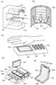


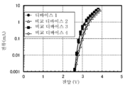

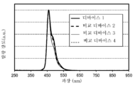
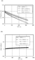


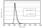


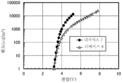


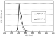

Classifications
-
- C—CHEMISTRY; METALLURGY
- C07—ORGANIC CHEMISTRY
- C07D—HETEROCYCLIC COMPOUNDS
- C07D209/00—Heterocyclic compounds containing five-membered rings, condensed with other rings, with one nitrogen atom as the only ring hetero atom
- C07D209/56—Ring systems containing three or more rings
- C07D209/80—[b, c]- or [b, d]-condensed
- C07D209/82—Carbazoles; Hydrogenated carbazoles
- C07D209/86—Carbazoles; Hydrogenated carbazoles with only hydrogen atoms, hydrocarbon or substituted hydrocarbon radicals, directly attached to carbon atoms of the ring system
-
- C—CHEMISTRY; METALLURGY
- C09—DYES; PAINTS; POLISHES; NATURAL RESINS; ADHESIVES; COMPOSITIONS NOT OTHERWISE PROVIDED FOR; APPLICATIONS OF MATERIALS NOT OTHERWISE PROVIDED FOR
- C09K—MATERIALS FOR MISCELLANEOUS APPLICATIONS, NOT PROVIDED FOR ELSEWHERE
- C09K11/00—Luminescent, e.g. electroluminescent, chemiluminescent materials
- C09K11/06—Luminescent, e.g. electroluminescent, chemiluminescent materials containing organic luminescent materials
-
- H01L51/0061—
-
- H01L51/0072—
-
- H01L51/5012—
-
- H01L51/5056—
-
- H—ELECTRICITY
- H10—SEMICONDUCTOR DEVICES; ELECTRIC SOLID-STATE DEVICES NOT OTHERWISE PROVIDED FOR
- H10K—ORGANIC ELECTRIC SOLID-STATE DEVICES
- H10K50/00—Organic light-emitting devices
- H10K50/10—OLEDs or polymer light-emitting diodes [PLED]
- H10K50/11—OLEDs or polymer light-emitting diodes [PLED] characterised by the electroluminescent [EL] layers
-
- H—ELECTRICITY
- H10—SEMICONDUCTOR DEVICES; ELECTRIC SOLID-STATE DEVICES NOT OTHERWISE PROVIDED FOR
- H10K—ORGANIC ELECTRIC SOLID-STATE DEVICES
- H10K50/00—Organic light-emitting devices
- H10K50/10—OLEDs or polymer light-emitting diodes [PLED]
- H10K50/14—Carrier transporting layers
- H10K50/15—Hole transporting layers
-
- H—ELECTRICITY
- H10—SEMICONDUCTOR DEVICES; ELECTRIC SOLID-STATE DEVICES NOT OTHERWISE PROVIDED FOR
- H10K—ORGANIC ELECTRIC SOLID-STATE DEVICES
- H10K85/00—Organic materials used in the body or electrodes of devices covered by this subclass
- H10K85/60—Organic compounds having low molecular weight
- H10K85/615—Polycyclic condensed aromatic hydrocarbons, e.g. anthracene
- H10K85/624—Polycyclic condensed aromatic hydrocarbons, e.g. anthracene containing six or more rings
-
- H—ELECTRICITY
- H10—SEMICONDUCTOR DEVICES; ELECTRIC SOLID-STATE DEVICES NOT OTHERWISE PROVIDED FOR
- H10K—ORGANIC ELECTRIC SOLID-STATE DEVICES
- H10K85/00—Organic materials used in the body or electrodes of devices covered by this subclass
- H10K85/60—Organic compounds having low molecular weight
- H10K85/631—Amine compounds having at least two aryl rest on at least one amine-nitrogen atom, e.g. triphenylamine
- H10K85/636—Amine compounds having at least two aryl rest on at least one amine-nitrogen atom, e.g. triphenylamine comprising heteroaromatic hydrocarbons as substituents on the nitrogen atom
-
- H—ELECTRICITY
- H10—SEMICONDUCTOR DEVICES; ELECTRIC SOLID-STATE DEVICES NOT OTHERWISE PROVIDED FOR
- H10K—ORGANIC ELECTRIC SOLID-STATE DEVICES
- H10K85/00—Organic materials used in the body or electrodes of devices covered by this subclass
- H10K85/60—Organic compounds having low molecular weight
- H10K85/649—Aromatic compounds comprising a hetero atom
- H10K85/657—Polycyclic condensed heteroaromatic hydrocarbons
- H10K85/6572—Polycyclic condensed heteroaromatic hydrocarbons comprising only nitrogen in the heteroaromatic polycondensed ring system, e.g. phenanthroline or carbazole
-
- C—CHEMISTRY; METALLURGY
- C09—DYES; PAINTS; POLISHES; NATURAL RESINS; ADHESIVES; COMPOSITIONS NOT OTHERWISE PROVIDED FOR; APPLICATIONS OF MATERIALS NOT OTHERWISE PROVIDED FOR
- C09K—MATERIALS FOR MISCELLANEOUS APPLICATIONS, NOT PROVIDED FOR ELSEWHERE
- C09K2211/00—Chemical nature of organic luminescent or tenebrescent compounds
- C09K2211/10—Non-macromolecular compounds
- C09K2211/1003—Carbocyclic compounds
- C09K2211/1011—Condensed systems
-
- C—CHEMISTRY; METALLURGY
- C09—DYES; PAINTS; POLISHES; NATURAL RESINS; ADHESIVES; COMPOSITIONS NOT OTHERWISE PROVIDED FOR; APPLICATIONS OF MATERIALS NOT OTHERWISE PROVIDED FOR
- C09K—MATERIALS FOR MISCELLANEOUS APPLICATIONS, NOT PROVIDED FOR ELSEWHERE
- C09K2211/00—Chemical nature of organic luminescent or tenebrescent compounds
- C09K2211/10—Non-macromolecular compounds
- C09K2211/1003—Carbocyclic compounds
- C09K2211/1014—Carbocyclic compounds bridged by heteroatoms, e.g. N, P, Si or B
-
- C—CHEMISTRY; METALLURGY
- C09—DYES; PAINTS; POLISHES; NATURAL RESINS; ADHESIVES; COMPOSITIONS NOT OTHERWISE PROVIDED FOR; APPLICATIONS OF MATERIALS NOT OTHERWISE PROVIDED FOR
- C09K—MATERIALS FOR MISCELLANEOUS APPLICATIONS, NOT PROVIDED FOR ELSEWHERE
- C09K2211/00—Chemical nature of organic luminescent or tenebrescent compounds
- C09K2211/10—Non-macromolecular compounds
- C09K2211/1018—Heterocyclic compounds
- C09K2211/1025—Heterocyclic compounds characterised by ligands
- C09K2211/1029—Heterocyclic compounds characterised by ligands containing one nitrogen atom as the heteroatom
-
- H—ELECTRICITY
- H10—SEMICONDUCTOR DEVICES; ELECTRIC SOLID-STATE DEVICES NOT OTHERWISE PROVIDED FOR
- H10K—ORGANIC ELECTRIC SOLID-STATE DEVICES
- H10K50/00—Organic light-emitting devices
- H10K50/10—OLEDs or polymer light-emitting diodes [PLED]
- H10K50/17—Carrier injection layers
-
- Y—GENERAL TAGGING OF NEW TECHNOLOGICAL DEVELOPMENTS; GENERAL TAGGING OF CROSS-SECTIONAL TECHNOLOGIES SPANNING OVER SEVERAL SECTIONS OF THE IPC; TECHNICAL SUBJECTS COVERED BY FORMER USPC CROSS-REFERENCE ART COLLECTIONS [XRACs] AND DIGESTS
- Y02—TECHNOLOGIES OR APPLICATIONS FOR MITIGATION OR ADAPTATION AGAINST CLIMATE CHANGE
- Y02E—REDUCTION OF GREENHOUSE GAS [GHG] EMISSIONS, RELATED TO ENERGY GENERATION, TRANSMISSION OR DISTRIBUTION
- Y02E10/00—Energy generation through renewable energy sources
- Y02E10/50—Photovoltaic [PV] energy
- Y02E10/549—Organic PV cells
Landscapes
- Chemical & Material Sciences (AREA)
- Organic Chemistry (AREA)
- Physics & Mathematics (AREA)
- Engineering & Computer Science (AREA)
- Materials Engineering (AREA)
- Spectroscopy & Molecular Physics (AREA)
- Optics & Photonics (AREA)
- Electroluminescent Light Sources (AREA)
- Light Receiving Elements (AREA)
- Indole Compounds (AREA)
- Manufacturing & Machinery (AREA)
- Computer Hardware Design (AREA)
- Microelectronics & Electronic Packaging (AREA)
- Power Engineering (AREA)
Abstract
Description
본 발명의 일 형태는 유기 화합물, 발광 디바이스, 발광 장치, 발광 모듈, 전자 기기, 및 조명 장치에 관한 것이다.One embodiment of the present invention relates to an organic compound, a light emitting device, a light emitting device, a light emitting module, an electronic device, and a lighting device.
또한 본 발명의 일 형태는 상술한 기술분야에 한정되지 않는다. 본 발명의 일 형태의 기술분야로서는, 반도체 장치, 표시 장치, 발광 장치, 축전 장치, 기억 장치, 전자 기기, 조명 장치, 입력 장치(예를 들어, 터치 센서 등), 입출력 장치(예를 들어 터치 패널 등), 이들의 구동 방법, 또는 이들의 제조 방법을 일례로서 들 수 있다.In addition, one embodiment of the present invention is not limited to the above-described technical field. As a technical field of one embodiment of the present invention, semiconductor devices, display devices, light emitting devices, power storage devices, memory devices, electronic devices, lighting devices, input devices (for example, touch sensors, etc.), input devices (for example, touch Panels, etc.), a driving method thereof, or a manufacturing method thereof may be mentioned as an example.
유기 일렉트로루미네선스(EL: Electro Luminescence) 현상을 이용한 발광 디바이스(유기 EL 디바이스, 유기 EL 소자라고도 함)의 연구 개발이 활발히 행해지고 있다. 유기 EL 디바이스의 기본적인 구성은 한 쌍의 전극 사이에 발광성 유기 화합물을 포함한 층(이후, 발광층이라고도 기재함)을 끼운 것이다. 이 유기 EL 디바이스에 전압을 인가함으로써, 발광성 유기 화합물로부터의 발광을 얻을 수 있다.Research and development of light-emitting devices (also referred to as organic EL devices and organic EL devices) using an organic electroluminescence (EL) phenomenon are being actively conducted. The basic configuration of an organic EL device is to sandwich a layer containing a light-emitting organic compound (hereinafter, also referred to as a light-emitting layer) between a pair of electrodes. By applying a voltage to this organic EL device, light emission from the luminescent organic compound can be obtained.
유기 EL 디바이스는 박형 경량화가 용이하고, 입력 신호에 대한 고속 응답이 가능하고, 직류 저전압 전원을 사용한 구동이 가능하다는 등의 특징을 가지므로 표시 장치에 적합하다.The organic EL device is suitable for a display device because it has features such as thinness, weight reduction, high speed response to an input signal, and driving using a DC low voltage power supply.
또한 유기 EL 디바이스는 막 형상으로 형성할 수 있기 때문에 면상(面狀)으로 발광을 얻을 수 있다. 따라서, 대면적의 발광 디바이스를 용이하게 형성할 수 있다. 이것은, LED(발광 다이오드)로 대표되는 점 광원 및 형광등으로 대표되는 선 광원에서는 얻기 어려운 특색이기 때문에 유기 EL 디바이스는 조명 장치 등에 응용할 수 있는 면 광원으로서의 이용 가치도 높다.In addition, since the organic EL device can be formed in a film shape, light emission can be obtained in the form of a plane. Thus, a large-area light emitting device can be easily formed. This is a characteristic that is difficult to obtain in a point light source typified by LEDs (light-emitting diodes) and a line light source typified by a fluorescent lamp. Therefore, the organic EL device has high utility value as a surface light source that can be applied to a lighting device or the like.
특허문헌 1에는 발광 디바이스에 사용할 수 있는 재료로서 정공 수송성이 높은 방향족 아민 화합물이 개시(開示)되어 있다.
본 발명의 일 형태는 신규 유기 화합물을 제공하는 것을 과제 중 하나로 한다. 또는 본 발명의 일 형태는 내열성이 높은 유기 화합물을 제공하는 것을 과제 중 하나로 한다. 또는 본 발명의 일 형태는 승화성이 높은 유기 화합물을 제공하는 것을 과제 중 하나로 한다. 또는 본 발명의 일 형태는 발광 디바이스에 사용할 수 있는 신규 유기 화합물을 제공하는 것을 과제 중 하나로 한다. 또는 본 발명의 일 형태는 발광 디바이스에서 정공 수송성 재료로서 사용할 수 있는 신규 유기 화합물을 제공하는 것을 과제 중 하나로 한다. 또는 본 발명의 일 형태는 발광 디바이스에서 발광 물질을 분산시키는 호스트 재료로서 사용할 수 있는 신규 유기 화합물을 제공하는 것을 과제 중 하나로 한다.One aspect of the present invention makes it one of the problems to provide a novel organic compound. Alternatively, one embodiment of the present invention makes it one of the problems to provide an organic compound having high heat resistance. Alternatively, one embodiment of the present invention makes it one of the objects to provide an organic compound having high sublimation properties. Another object of one embodiment of the present invention is to provide a novel organic compound that can be used in a light emitting device. Another object of one embodiment of the present invention is to provide a novel organic compound that can be used as a hole transport material in a light emitting device. Another object of the present invention is to provide a novel organic compound that can be used as a host material for dispersing a light-emitting substance in a light-emitting device.
또는 본 발명의 일 형태는 발광 효율이 높은 발광 디바이스를 제공하는 것을 과제 중 하나로 한다. 또는 본 발명의 일 형태는 구동 전압이 낮은 발광 디바이스를 제공하는 것을 과제 중 하나로 한다. 또는 본 발명의 일 형태는 수명이 긴 발광 디바이스를 제공하는 것을 과제 중 하나로 한다. 또는 본 발명의 일 형태는 내열성이 높은 발광 디바이스를 제공하는 것을 과제 중 하나로 한다.Another object of one embodiment of the present invention is to provide a light emitting device having high luminous efficiency. Another object of the present invention is to provide a light emitting device having a low driving voltage. Another object of one embodiment of the present invention is to provide a light emitting device having a long life. Another object of one embodiment of the present invention is to provide a light emitting device having high heat resistance.
또한 이들 과제의 기재는 다른 과제의 존재를 방해하는 것은 아니다. 본 발명의 일 형태는 반드시 이들 과제 모두를 해결할 필요는 없는 것으로 한다. 명세서, 도면, 청구범위의 기재로부터 이들 외의 과제를 추출할 수 있다.In addition, description of these problems does not interfere with the existence of other problems. It is assumed that one embodiment of the present invention does not necessarily have to solve all of these problems. Subjects other than these can be extracted from the description of the specification, drawings, and claims.
본 발명의 일 형태는 일반식(G0)으로 나타내어지는 유기 화합물이다.One aspect of the present invention is an organic compound represented by general formula (G0).
[화학식 1][Formula 1]

일반식(G0)에서, R1 내지 R5는 이들 중 하나가 일반식(A)을 나타내고, 나머지는 각각 독립적으로 수소, 탄소수 1 내지 6의 알킬기, 탄소수 3 내지 6의 사이클로알킬기, 또는 치환 또는 비치환된 탄소수 6 내지 13의 아릴기를 나타내고, R6 내지 R13, R21 내지 R29, R31 내지 R39, 및 R41 내지 R48은 각각 독립적으로 수소, 탄소수 1 내지 6의 알킬기, 탄소수 3 내지 6의 사이클로알킬기, 또는 치환 또는 비치환된 탄소수 6 내지 13의 아릴기를 나타낸다. R21과 R22는 서로 결합하여 스파이로 고리를 형성하여도 좋다.In the general formula (G0), one of R 1 to R 5 represents the general formula (A), and the others are each independently hydrogen, an alkyl group having 1 to 6 carbon atoms, a cycloalkyl group having 3 to 6 carbon atoms, or a substituted or Represents an unsubstituted aryl group having 6 to 13 carbon atoms, and R 6 to R 13 , R 21 to R 29 , R 31 to R 39 , and R 41 to R 48 are each independently hydrogen, an alkyl group having 1 to 6 carbon atoms, and It represents a cycloalkyl group of 3 to 6 or a substituted or unsubstituted aryl group having 6 to 13 carbon atoms. R 21 and R 22 may be bonded to each other to form a spy ring.
본 발명의 일 형태는 일반식(G1)으로 나타내어지는 유기 화합물이다.One aspect of the present invention is an organic compound represented by General Formula (G1).
[화학식 2][Formula 2]

일반식(G1)에서, R2 내지 R13, R21 내지 R29, R31 내지 R39, 및 R41 내지 R48은 각각 독립적으로 수소, 탄소수 1 내지 6의 알킬기, 탄소수 3 내지 6의 사이클로알킬기, 또는 치환 또는 비치환된 탄소수 6 내지 13의 아릴기를 나타낸다. R21과 R22는 서로 결합하여 스파이로 고리를 형성하여도 좋다.In the general formula (G1), R 2 to R 13 , R 21 to R 29 , R 31 to R 39 , and R 41 to R 48 are each independently hydrogen, an alkyl group having 1 to 6 carbon atoms, a cyclo of 3 to 6 carbon atoms It represents an alkyl group or a substituted or unsubstituted aryl group having 6 to 13 carbon atoms. R 21 and R 22 may be bonded to each other to form a spy ring.
일반식(G0) 및 일반식(G1)에서, R35 내지 R39 중 어느 하나는 치환 또는 비치환된 페닐기 혹은 치환 또는 비치환된 나프틸기를 나타내는 것이 바람직하다.In general formula (G0) and general formula (G1), it is preferable that any one of R 35 to R 39 represents a substituted or unsubstituted phenyl group or a substituted or unsubstituted naphthyl group.
일반식(G0) 및 일반식(G1)에서, R21과 R22는 동일하고, 또한 탄소수 1 내지 6의 알킬기 혹은 치환 또는 비치환된 페닐기를 나타내는 것이 바람직하다.In the general formula (G0) and the general formula (G1), it is preferable that R 21 and R 22 are the same and represent an alkyl group having 1 to 6 carbon atoms or a substituted or unsubstituted phenyl group.
일반식(G0) 및 일반식(G1)에서, R21 및 R22는 모두 메틸기를 나타내는 것이 바람직하다. 또는 R21 및 R22는 모두 비치환된 페닐기를 나타내는 것이 바람직하다. 또는 R21과 R22는 서로 결합하여 스파이로 고리를 형성하는 것이 바람직하다. 예를 들어 R21 및 R22는 모두 치환 또는 비치환된 페닐기이고, 페닐기들이 서로 결합하여 스파이로바이플루오렌 고리를 형성하는 것이 바람직하다.In general formula (G0) and general formula (G1), it is preferable that both R 21 and R 22 represent a methyl group. Alternatively, it is preferable that both R 21 and R 22 represent an unsubstituted phenyl group. Or R 21 and R 22 are preferably bonded to each other to form a ring with a spy. For example, R 21 and R 22 are both substituted or unsubstituted phenyl groups, and it is preferable that the phenyl groups are bonded to each other to form a spirobifluorene ring.
일반식(G0) 및 일반식(G1)에서, R41 내지 R48은 각각 독립적으로 수소, 메틸기, tert-뷰틸기, 혹은 치환 또는 비치환된 페닐기를 나타내는 것이 바람직하다.In the general formula (G0) and the general formula (G1), it is preferable that R 41 to R 48 each independently represent hydrogen, a methyl group, a tert-butyl group, or a substituted or unsubstituted phenyl group.
본 발명의 일 형태는 상술한 어느 구성의 유기 화합물을 가지는 발광 디바이스, 수광 디바이스, 또는 수광 및 발광 디바이스이다.One embodiment of the present invention is a light-emitting device, a light-receiving device, or a light-receiving and light-emitting device having an organic compound of any of the above-described configurations.
본 발명의 일 형태는 한 쌍의 전극 사이에 유기 화합물을 포함한 층을 가지고, 유기 화합물을 포함한 층은 상술한 어느 구성을 가지는 유기 화합물을 포함하는 발광 디바이스, 수광 디바이스, 또는 수광 및 발광 디바이스이다.One embodiment of the present invention includes a layer containing an organic compound between a pair of electrodes, and the layer containing the organic compound is a light-emitting device, a light-receiving device, or a light-receiving and light-emitting device containing an organic compound having any of the above-described configurations.
본 발명의 일 형태는 한 쌍의 전극 사이에 유기 화합물을 포함한 층을 가지고, 유기 화합물을 포함한 층은 발광층 및 정공 수송층을 가지고, 발광층 및 정공 수송층 중 적어도 하나는 상술한 어느 구성을 가지는 유기 화합물을 포함하는 발광 디바이스이다.One embodiment of the present invention includes a layer containing an organic compound between a pair of electrodes, the layer containing the organic compound has an emission layer and a hole transport layer, and at least one of the emission layer and the hole transport layer comprises an organic compound having any of the above-described configurations. It is a light emitting device including.
본 발명의 일 형태는 상술한 어느 구성을 가지는 발광 디바이스와, 트랜지스터 및 기판 중 한쪽 또는 양쪽을 포함하는 발광 장치이다.One embodiment of the present invention is a light-emitting device including a light-emitting device having any of the above-described configurations, and one or both of a transistor and a substrate.
본 발명의 일 형태는 상기 발광 장치를 가지고, 플렉시블 프린트 회로 기판(Flexible Printed Circuit, 이후 FPC라고 기재함) 또는 TCP(Tape Carrier Package) 등의 커넥터가 장착된 발광 모듈, 또는 COG(Chip On Glass) 방식 또는 COF(Chip On Film) 방식 등에 의하여 집적 회로(IC)가 실장된 발광 모듈 등의 발광 모듈이다. 또한 본 발명의 일 형태의 발광 모듈은 커넥터 및 IC 중 한쪽만을 가져도 좋고 양쪽을 가져도 좋다.One embodiment of the present invention has the above light emitting device, a light emitting module equipped with a connector such as a flexible printed circuit board (Flexible Printed Circuit, hereinafter referred to as FPC) or TCP (Tape Carrier Package), or COG (Chip On Glass) This is a light-emitting module such as a light-emitting module in which an integrated circuit (IC) is mounted by a method or a chip on film (COF) method. Further, the light emitting module of one embodiment of the present invention may have only one or both of the connector and the IC.
본 발명의 일 형태는 상기 구성 중 어느 것을 가지는 발광 모듈과, 안테나, 배터리, 하우징, 카메라, 스피커, 마이크로폰, 및 조작 버튼 중 적어도 하나를 가지는 전자 기기이다.One aspect of the present invention is an electronic device having a light emitting module having any of the above configurations, and at least one of an antenna, a battery, a housing, a camera, a speaker, a microphone, and an operation button.
본 발명의 일 형태는 상기 발광 디바이스와, 하우징, 커버, 및 지지대 중 적어도 하나를 가지는 조명 장치이다.One aspect of the present invention is a lighting device having at least one of the light emitting device, a housing, a cover, and a support.
본 발명의 일 형태에 의하여 신규 유기 화합물을 제공할 수 있다. 본 발명의 일 형태에 의하여 내열성이 높은 유기 화합물을 제공할 수 있다. 본 발명의 일 형태에 의하여 승화성이 높은 유기 화합물을 제공할 수 있다. 본 발명의 일 형태에 의하여 발광 디바이스에 사용할 수 있는 신규 유기 화합물을 제공할 수 있다. 본 발명의 일 형태에 의하여 발광 디바이스에서 정공 수송성 재료로서 사용할 수 있는 신규 유기 화합물을 제공할 수 있다. 본 발명의 일 형태에 의하여 발광 디바이스에서 발광 물질을 분산시키는 호스트 재료로서 사용할 수 있는 신규 유기 화합물을 제공할 수 있다.According to one embodiment of the present invention, a novel organic compound can be provided. According to one embodiment of the present invention, an organic compound having high heat resistance can be provided. According to one embodiment of the present invention, an organic compound having high sublimation properties can be provided. According to one embodiment of the present invention, a novel organic compound that can be used in a light emitting device can be provided. According to one embodiment of the present invention, a novel organic compound that can be used as a hole transport material in a light emitting device can be provided. According to one embodiment of the present invention, it is possible to provide a novel organic compound that can be used as a host material for dispersing light-emitting substances in a light-emitting device.
본 발명의 일 형태는 발광 효율이 높은 발광 디바이스를 제공할 수 있다. 본 발명의 일 형태에 의하여 구동 전압이 낮은 발광 디바이스를 제공할 수 있다. 본 발명의 일 형태에 의하여 수명이 긴 발광 디바이스를 제공할 수 있다. 본 발명의 일 형태에 의하여 내열성이 높은 발광 디바이스를 제공할 수 있다.One embodiment of the present invention can provide a light emitting device having high luminous efficiency. According to one embodiment of the present invention, a light emitting device having a low driving voltage can be provided. According to one embodiment of the present invention, a light emitting device having a long life can be provided. According to one embodiment of the present invention, a light emitting device having high heat resistance can be provided.
또한 이들 효과의 기재는 다른 효과의 존재를 방해하는 것은 아니다. 본 발명의 일 형태는 이들 효과 모두를 반드시 가질 필요는 없다. 명세서, 도면, 청구범위의 기재로부터 이들 외의 효과를 추출할 수 있다.In addition, description of these effects does not interfere with the existence of other effects. One embodiment of the present invention need not necessarily have all of these effects. Effects other than these can be extracted from the description of the specification, drawings, and claims.
도 1의 (A) 내지 (D)는 발광 디바이스의 일례를 나타낸 단면도이다.
도 2의 (A)는 발광 장치의 일례를 나타낸 상면도이고, 도 2의 (B) 및 (C)는 발광 장치의 일례를 나타낸 단면도이다.
도 3의 (A) 및 (C)는 발광 장치의 일례를 나타낸 단면도이고, 도 3의 (B)는 발광 디바이스의 일례를 나타낸 단면도이다.
도 4의 (A) 및 (B)는 발광 장치의 일례를 나타낸 단면도이다.
도 5의 (A)는 발광 장치의 일례를 나타낸 상면도이고, 도 5의 (B)는 발광 장치의 일례를 나타낸 단면도이고, 도 5의 (C) 및 (D)는 트랜지스터의 일례를 나타낸 단면도이다.
도 6의 (A) 내지 (D)는 전자 기기의 일례를 나타낸 도면이다.
도 7의 (A) 내지 (F)는 전자 기기의 일례를 나타낸 도면이다.
도 8의 (A) 내지 (C)는 전자 기기의 일례를 나타낸 도면이다.
도 9의 (A) 내지 (E)는 전자 기기의 일례를 나타낸 도면이다.
도 10의 (A) 및 (B)는 구조식(100)으로 나타내어지는 유기 화합물의 자외·가시 흡수 스펙트럼 및 발광 스펙트럼이다.
도 11은 실시예의 발광 디바이스를 나타낸 단면도이다.
도 12는 실시예 2의 발광 디바이스의 휘도-전류 효율 특성을 나타낸 도면이다.
도 13은 실시예 2의 발광 디바이스의 전압-휘도 특성을 나타낸 도면이다.
도 14는 실시예 2의 발광 디바이스의 전압-전류 특성을 나타낸 도면이다.
도 15는 실시예 2의 발광 디바이스의 휘도-외부 양자 효율 특성을 나타낸 도면이다.
도 16은 실시예 2의 발광 디바이스의 발광 스펙트럼을 나타낸 도면이다.
도 17의 (A) 및 (B)는 실시예 2의 발광 디바이스의 신뢰성 시험의 결과를 나타낸 도면이다.
도 18은 실시예 3의 발광 디바이스의 휘도-전류 효율 특성을 나타낸 도면이다.
도 19는 실시예 3의 발광 디바이스의 전압-휘도 특성을 나타낸 도면이다.
도 20은 실시예 3의 발광 디바이스의 전압-전류 특성을 나타낸 도면이다.
도 21은 실시예 3의 발광 디바이스의 휘도-외부 양자 효율 특성을 나타낸 도면이다.
도 22는 실시예 3의 발광 디바이스의 발광 스펙트럼을 나타낸 도면이다.
도 23의 (A) 및 (B)는 실시예 3의 발광 디바이스의 신뢰성 시험의 결과를 나타낸 도면이다.
도 24는 실시예 4의 발광 디바이스의 휘도-전류 효율 특성을 나타낸 도면이다.
도 25는 실시예 4의 발광 디바이스의 전압-휘도 특성을 나타낸 도면이다.
도 26은 실시예 4의 발광 디바이스의 전압-전류 특성을 나타낸 도면이다.
도 27은 실시예 4의 발광 디바이스의 휘도-외부 양자 효율 특성을 나타낸 도면이다.
도 28은 실시예 4의 발광 디바이스의 발광 스펙트럼을 나타낸 도면이다.
도 29의 (A) 및 (B)는 실시예 4의 발광 디바이스의 신뢰성 시험의 결과를 나타낸 도면이다.1A to 1D are cross-sectional views showing an example of a light emitting device.
2A is a top view showing an example of a light emitting device, and FIGS. 2B and 2C are cross-sectional views illustrating an example of a light emitting device.
3A and 3C are cross-sectional views showing an example of a light emitting device, and FIG. 3B is a cross-sectional view showing an example of a light emitting device.
4A and 4B are cross-sectional views showing an example of a light emitting device.
5A is a top view showing an example of a light emitting device, FIG. 5B is a cross-sectional view showing an example of a light emitting device, and FIGS. 5C and 5D are cross-sectional views showing an example of a transistor. to be.
6A to 6D are diagrams showing an example of an electronic device.
7A to 7F are diagrams showing an example of an electronic device.
8A to 8C are diagrams showing an example of an electronic device.
9A to 9E are diagrams showing an example of an electronic device.
10A and 10B are ultraviolet and visible absorption spectra and emission spectra of the organic compound represented by the structural formula (100).
11 is a cross-sectional view showing the light emitting device of the embodiment.
12 is a diagram showing the luminance-current efficiency characteristics of the light emitting device of Example 2. FIG.
13 is a diagram showing voltage-luminance characteristics of the light emitting device of Example 2. FIG.
14 is a diagram showing voltage-current characteristics of the light emitting device of Example 2. FIG.
15 is a diagram showing luminance-external quantum efficiency characteristics of the light emitting device of Example 2. FIG.
16 is a diagram showing an emission spectrum of the light emitting device of Example 2. FIG.
17A and 17B are diagrams showing the results of a reliability test of the light emitting device of Example 2. FIG.
18 is a diagram showing the luminance-current efficiency characteristics of the light emitting device of Example 3. FIG.
19 is a diagram showing voltage-luminance characteristics of the light emitting device of Example 3. FIG.
20 is a diagram showing voltage-current characteristics of the light emitting device of Example 3. FIG.
21 is a diagram showing luminance-external quantum efficiency characteristics of the light emitting device of Example 3. FIG.
22 is a diagram showing an emission spectrum of the light emitting device of Example 3. FIG.
23A and 23B are diagrams showing the results of a reliability test of the light emitting device of Example 3. FIG.
24 is a diagram showing the luminance-current efficiency characteristics of the light emitting device of Example 4. FIG.
25 is a diagram showing voltage-luminance characteristics of the light emitting device of Example 4. FIG.
26 is a diagram showing the voltage-current characteristics of the light emitting device of Example 4. FIG.
27 is a diagram showing the luminance-external quantum efficiency characteristics of the light emitting device of Example 4. FIG.
28 is a diagram showing an emission spectrum of the light emitting device of Example 4. FIG.
29A and 29B are diagrams showing the results of a reliability test of the light emitting device of Example 4.
실시형태에 대하여 도면을 참조하여 자세히 설명한다. 다만, 본 발명은 아래의 설명에 한정되지 않고, 본 발명의 취지 및 그 범위에서 벗어남이 없이 그 형태 및 자세한 사항을 다양하게 변경할 수 있다는 것은 통상의 기술자라면 용이하게 이해할 수 있다. 따라서 본 발명은 이하의 실시형태의 기재 내용에 한정하여 해석되는 것은 아니다.An embodiment will be described in detail with reference to the drawings. However, the present invention is not limited to the description below, and it can be easily understood by those of ordinary skill in the art that the form and details can be variously changed without departing from the spirit and scope of the present invention. Therefore, the present invention is not interpreted as being limited to the description of the following embodiments.
또한 아래에서 설명하는 발명의 구성에서, 동일한 부분 또는 같은 기능을 가지는 부분에는 동일한 부호를 다른 도면 간에서 공통적으로 사용하고, 그 반복 설명은 생략한다. 또한 같은 기능을 가지는 부분을 가리키는 경우에는, 같은 해치 패턴으로 하고, 특별히 부호를 붙이지 않는 경우가 있다.In addition, in the configuration of the invention described below, the same reference numerals are used in common between different drawings for the same part or parts having the same function, and repeated description thereof will be omitted. In addition, when referring to a portion having the same function, the same hatch pattern may be used, and no special symbol may be attached.
또한 도면에 나타낸 각 구성의 위치, 크기, 범위 등은 이해를 쉽게 하기 위하여 실제의 위치, 크기, 범위 등을 나타내지 않는 경우가 있다. 그러므로 개시된 발명은 반드시 도면에 개시된 위치, 크기, 범위 등에 한정되지 않는다.In addition, the location, size, range, etc. of each component shown in the drawings may not represent the actual location, size, range, etc. for easy understanding. Therefore, the disclosed invention is not necessarily limited to the position, size, and range disclosed in the drawings.
또한 "막"이라는 용어와 "층"이라는 용어는 경우 또는 상황에 따라 서로 바뀔 수 있다. 예를 들어 "도전층"이라는 용어를 "도전막"이라는 용어로 바꿀 수 있다. 또는 예를 들어 "절연막"이라는 용어를 "절연층"이라는 용어로 바꿀 수 있다.Also, the terms "film" and "layer" may be interchanged with each other depending on the case or situation. For example, the term "conductive layer" can be replaced with the term "conductive film". Or, for example, the term "insulation layer" may be replaced with the term "insulation layer".
(실시형태 1)(Embodiment 1)
본 실시형태에서는 본 발명의 일 형태의 유기 화합물에 대하여 설명한다.In this embodiment, an organic compound of one embodiment of the present invention will be described.
[본 발명의 일 형태의 유기 화합물의 구조][Structure of organic compound of one embodiment of the present invention]
본 발명의 일 형태의 유기 화합물은 3급 아민이고, 아민의 질소에는 바이페닐 골격의 오쏘 위치와, 플루오렌 골격과, 터페닐렌 골격이 결합되고, 상기 터페닐렌 골격의 아민의 질소로부터 가장 먼 페닐렌기에는 카바졸 골격이 결합된다.The organic compound of one embodiment of the present invention is a tertiary amine, and the ortho position of the biphenyl skeleton, the fluorene skeleton, and the terphenylene skeleton are bonded to the nitrogen of the amine. The carbazole skeleton is attached to the distant phenylene group.
자동차용 등 고온 환경하에서 사용되는 발광 디바이스에는 높은 내열성이 요구된다. 또한 유리 프릿을 사용한 밀봉 공정 등 제품의 제작 공정 중에 고온이 가해지는 경우에도 발광 디바이스에는 높은 내열성이 요구된다. 따라서, 발광 디바이스에 사용되는 재료에는 유리 전이 온도(Tg)가 100℃ 이상, 나아가서는 120℃ 이상인 것이 요구되는 경우가 있다. 본 발명의 일 형태에서는 유기 화합물의 Tg를 100℃ 이상, 나아가서는 120℃ 이상으로 할 수 있으므로 높은 내열성이 요구되는 발광 디바이스에 적합한 재료를 제공할 수 있다. 한편, 발광 디바이스의 제작은 진공 증착에 의하여 수행되는 경우가 많다. 이 경우, 발광 디바이스에 사용되는 재료는 높은 내열성과 높은 승화성의 양쪽 모두를 가질 필요가 있고, 승화 온도는 500℃ 이하인 것이 바람직하고, 더 바람직하게는 400℃ 이하이다. 본 발명의 일 형태에서는 높은 내열성뿐만 아니라 높은 승화성도 가지는 재료를 제공할 수 있기 때문에 디바이스 제작의 관점에서 높은 생산성을 가지는 재료를 제공할 수 있다.High heat resistance is required for light emitting devices used in high temperature environments such as automobiles. In addition, high heat resistance is required for the light emitting device even when a high temperature is applied during a product manufacturing process such as a sealing process using a glass frit. Therefore, the material used for the light emitting device may be required to have a glass transition temperature (Tg) of 100°C or higher and further 120°C or higher. In one embodiment of the present invention, since the Tg of the organic compound can be set to 100°C or higher, further to 120°C or higher, a material suitable for a light-emitting device requiring high heat resistance can be provided. On the other hand, manufacturing of a light emitting device is often performed by vacuum evaporation. In this case, the material used for the light emitting device needs to have both high heat resistance and high sublimation property, and the sublimation temperature is preferably 500°C or less, and more preferably 400°C or less. In one embodiment of the present invention, since a material having not only high heat resistance but also high sublimation property can be provided, a material having high productivity from the viewpoint of device manufacturing can be provided.
본 발명의 일 형태의 유기 화합물은 정공 수송성 및 전자 블로킹성이 높다. 본 발명의 일 형태의 유기 화합물은 발광 디바이스에서 정공 수송성 재료로서 사용할 수 있다. 또한 본 발명의 일 형태의 유기 화합물은 발광 디바이스에서 발광 물질을 분산시키는 호스트 재료로서 사용할 수 있다. 본 발명의 일 형태의 유기 화합물을 사용함으로써 발광 디바이스의 발광 효율 및 신뢰성을 높일 수 있다.The organic compound of one embodiment of the present invention has high hole transport properties and electron blocking properties. The organic compound of one embodiment of the present invention can be used as a hole transport material in a light emitting device. In addition, the organic compound of one embodiment of the present invention can be used as a host material for dispersing light-emitting substances in a light-emitting device. By using the organic compound of one embodiment of the present invention, the luminous efficiency and reliability of the light emitting device can be improved.
또한 본 발명의 일 형태의 유기 화합물은 유기 포토다이오드 등의 수광 디바이스나, 발광 및 수광의 양쪽의 기능을 가지는 수광 및 발광 디바이스에서도 캐리어 수송성 재료(정공 수송성 재료)로서 사용할 수 있다.In addition, the organic compound of one embodiment of the present invention can be used as a carrier-transporting material (hole-transporting material) in a light-receiving device such as an organic photodiode, or a light-receiving and light-emitting device having both functions of light emission and light reception.
구체적으로는 본 발명의 일 형태는 일반식(G0)으로 나타내어지는 유기 화합물이다. 또한 이후의 일반식으로 나타내어지는 구조의 유기 화합물뿐만 아니라 상기 구조의 발광 디바이스용 재료 및 수광 디바이스용 재료도 각각 본 발명의 일 형태이다.Specifically, one embodiment of the present invention is an organic compound represented by general formula (G0). Further, not only the organic compound of the structure represented by the following general formula, but also the material for a light-emitting device and a material for a light-receiving device having the above structure are one embodiment of the present invention.
[화학식 3][Formula 3]

일반식(G0)에서, R1 내지 R5는 이들 중 하나가 일반식(A)을 나타내고, 나머지는 각각 독립적으로 수소, 탄소수 1 내지 6의 알킬기, 탄소수 3 내지 6의 사이클로알킬기, 또는 치환 또는 비치환된 탄소수 6 내지 13의 아릴기를 나타내고, R6 내지 R13, R21 내지 R29, R31 내지 R39, 및 R41 내지 R48은 각각 독립적으로 수소, 탄소수 1 내지 6의 알킬기, 탄소수 3 내지 6의 사이클로알킬기, 또는 치환 또는 비치환된 탄소수 6 내지 13의 아릴기를 나타내고, R21과 R22는 서로 결합하여 스파이로 고리를 형성하여도 좋다.In the general formula (G0), one of R 1 to R 5 represents the general formula (A), and the others are each independently hydrogen, an alkyl group having 1 to 6 carbon atoms, a cycloalkyl group having 3 to 6 carbon atoms, or a substituted or Represents an unsubstituted aryl group having 6 to 13 carbon atoms, and R 6 to R 13 , R 21 to R 29 , R 31 to R 39 , and R 41 to R 48 are each independently hydrogen, an alkyl group having 1 to 6 carbon atoms, and It represents a cycloalkyl group of 3 to 6 or a substituted or unsubstituted aryl group having 6 to 13 carbon atoms, and R 21 and R 22 may be bonded to each other to form a spy ring.
일반식(G0)으로 나타내어지는 유기 화합물 중 일반식(G1)으로 나타내어지는 유기 화합물이 더 바람직하다. 터페닐렌 골격의 파라 위치에 카바졸릴기가 결합되는 분자 구조로 함으로써 터페닐렌 골격의 오쏘 위치 또는 메타 위치에 카바졸릴기가 결합되는 분자 구조와 비교하여 유기 화합물의 내열성을 높일 수 있다.Of the organic compounds represented by the general formula (G0), the organic compounds represented by the general formula (G1) are more preferable. By having a molecular structure in which a carbazolyl group is bonded to the para position of the terphenylene skeleton, it is possible to increase the heat resistance of the organic compound compared to a molecular structure in which a carbazolyl group is bonded to the ortho position or meta position of the terphenylene skeleton.
[화학식 4][Formula 4]

일반식(G1)에서, R2 내지 R13, R21 내지 R29, R31 내지 R39, 및 R41 내지 R48은 각각 독립적으로 수소, 탄소수 1 내지 6의 알킬기, 탄소수 3 내지 6의 사이클로알킬기, 또는 치환 또는 비치환된 탄소수 6 내지 13의 아릴기를 나타내고, R21과 R22는 서로 결합하여 스파이로 고리를 형성하여도 좋다.In the general formula (G1), R 2 to R 13 , R 21 to R 29 , R 31 to R 39 , and R 41 to R 48 are each independently hydrogen, an alkyl group having 1 to 6 carbon atoms, a cyclo of 3 to 6 carbon atoms It represents an alkyl group or a substituted or unsubstituted aryl group having 6 to 13 carbon atoms, and R 21 and R 22 may be bonded to each other to form a spy ring.
R35 내지 R39 중 어느 하나가 치환 또는 비치환된 페닐기 혹은 치환 또는 비치환된 나프틸기를 나타내는 것이 바람직하다. 이에 의하여, 유기 화합물의 내열성을 높일 수 있다.It is preferable that any one of R 35 to R 39 represents a substituted or unsubstituted phenyl group or a substituted or unsubstituted naphthyl group. Thereby, the heat resistance of the organic compound can be improved.
플루오렌일기의 9위치가 수소인 경우, 상기 수소의 산성도가 높아져 발광 디바이스의 신뢰성이 저하될 우려가 있기 때문에 플루오렌일기의 9위치인 R21과 R22는 수소가 아니라 치환기를 나타내는 것이 바람직하다. 일반식(G1)으로 나타내어지는 유기 화합물의 내열성과 승화성을 고려하면, R21과 R22는 각각 독립적으로 탄소수 1 내지 6의 알킬기, 혹은 치환 또는 비치환된 페닐기를 나타내는 것이 바람직하다. 또는 R21과 R22는 동일하고, 또한 탄소수 1 내지 6의 알킬기 혹은 치환 또는 비치환된 페닐기를 나타내는 것이 바람직하다.When the 9-position of the fluorenyl group is hydrogen, the acidity of the hydrogen increases and the reliability of the light-emitting device may be lowered. Therefore, it is preferable that R 21 and R 22 in the 9-position of the fluorenyl group represent a substituent rather than hydrogen . In view of the heat resistance and sublimation property of the organic compound represented by the general formula (G1), it is preferable that R 21 and R 22 each independently represent an alkyl group having 1 to 6 carbon atoms or a substituted or unsubstituted phenyl group. Or it is preferable that R 21 and R 22 are the same and further represent an alkyl group having 1 to 6 carbon atoms or a substituted or unsubstituted phenyl group.
또한 합성 비용의 관점에서 R21과 R22는 동일한 것이 바람직하다.Moreover, it is preferable that R 21 and R 22 are the same from the viewpoint of synthesis cost.
R21 및 R22는 모두 메틸기를 나타내는 것이 바람직하다. 이에 의하여, 유기 화합물의 승화성을 높일 수 있다. 또는 R21 및 R22는 모두 무치환된 페닐기를 나타내는 것이 바람직하다. 이에 의하여, 유기 화합물의 내열성을 높일 수 있다.It is preferable that both R 21 and R 22 represent a methyl group. Thereby, the sublimation property of an organic compound can be improved. Alternatively, it is preferable that both R 21 and R 22 represent an unsubstituted phenyl group. Thereby, the heat resistance of the organic compound can be improved.
또는 R21 및 R22는 높은 내열성 또는 높은 신뢰성을 가지기 때문에 서로 결합하여 스파이로 고리를 형성하는 것이 바람직하다. 예를 들어 R21 및 R22는 모두 치환 또는 비치환된 페닐기이고, 페닐기들이 서로 결합하여 스파이로바이플루오렌 고리를 형성하는 것이 바람직하다.Alternatively, since R 21 and R 22 have high heat resistance or high reliability, they are preferably bonded to each other to form a spy ring. For example, R 21 and R 22 are both substituted or unsubstituted phenyl groups, and it is preferable that the phenyl groups are bonded to each other to form a spirobifluorene ring.
R41 내지 R48은 높은 승화성 또는 높은 신뢰성을 가지기 때문에 각각 독립적으로 수소, 메틸기, tert-뷰틸기, 또는 치환 또는 비치환된 페닐기를 나타내는 것이 바람직하다.Since R 41 to R 48 have high sublimability or high reliability, it is preferable that each independently represent hydrogen, a methyl group, a tert-butyl group, or a substituted or unsubstituted phenyl group.
일반식(G0) 및 일반식(G1)에서의 탄소수 1 내지 6의 알킬기로서는, 메틸기, 에틸기, 프로필기, 아이소프로필기, 뷰틸기, sec-뷰틸기, 아이소뷰틸기, tert-뷰틸기, 펜틸기, 아이소펜틸기, sec-펜틸기, tert-펜틸기, 네오펜틸기, 헥실기, 아이소헥실기, 3-메틸펜틸기, 2-메틸펜틸기, 2-에틸뷰틸기, 1,2-다이메틸뷰틸기, 2,3-다이메틸뷰틸기, n-헵틸기 등을 들 수 있다.Examples of the alkyl group having 1 to 6 carbon atoms in the general formula (G0) and general formula (G1) include methyl group, ethyl group, propyl group, isopropyl group, butyl group, sec-butyl group, isobutyl group, tert-butyl group, pen Tyl group, isopentyl group, sec-pentyl group, tert-pentyl group, neopentyl group, hexyl group, isohexyl group, 3-methylpentyl group, 2-methylpentyl group, 2-ethylbutyl group, 1,2-di Methylbutyl group, 2,3-dimethylbutyl group, n-heptyl group, etc. are mentioned.
일반식(G0) 및 일반식(G1)에서의 탄소수 3 내지 6의 사이클로알킬기로서는, 사이클로프로필기, 사이클로뷰틸기, 사이클로펜틸기, 사이클로헥실기 등을 들 수 있다.Examples of the cycloalkyl group having 3 to 6 carbon atoms in the general formula (G0) and the general formula (G1) include a cyclopropyl group, a cyclobutyl group, a cyclopentyl group, and a cyclohexyl group.
일반식(G0) 및 일반식(G1)에서의 치환 또는 비치환된 탄소수 6 내지 13의 아릴기로서는, 페닐기, o-톨릴기, m-톨릴기, p-톨릴기, 메시틸기, o-바이페닐기, m-바이페닐기, p-바이페닐기, 1-나프틸기, 2-나프틸기, 9H-플루오렌일기, 9,9-다이메틸-9H-플루오렌일기, 9,9'-스파이로바이[9H-플루오렌]-일기 등을 들 수 있다.Examples of the substituted or unsubstituted aryl group having 6 to 13 carbon atoms in the general formula (G0) and the general formula (G1) include phenyl group, o-tolyl group, m-tolyl group, p-tolyl group, mesityl group, o-by Phenyl group, m-biphenyl group, p-biphenyl group, 1-naphthyl group, 2-naphthyl group, 9H-fluorenyl group, 9,9-dimethyl-9H-fluorenyl group, 9,9'-spirobi[ 9H-fluorene]-yl group, and the like.
일반식(G0) 및 일반식(G1)의 "치환 또는 비치환된 X"(X는 각종 고리, 골격, 기 등)에서, X가 치환기를 가지는 경우, 상기 치환기로서는, 메틸기, 에틸기, 프로필기, 아이소프로필기, 뷰틸기, 아이소뷰틸기, sec-뷰틸기, tert-뷰틸기, 펜틸기, 헥실기 등의 탄소수 1 내지 6의 알킬기와, 사이클로프로필기, 사이클로뷰틸기, 사이클로펜틸기, 사이클로헥실기 등의 탄소수 3 내지 6의 사이클로알킬기와, 페닐기, 나프틸기, 바이페닐기 등의 탄소수 6 내지 13의 아릴기 등을 들 수 있다.In the "substituted or unsubstituted X" (X is various rings, skeletons, groups, etc.) of the general formula (G0) and general formula (G1), when X has a substituent, as the substituent, a methyl group, an ethyl group, a propyl group , Isopropyl group, butyl group, isobutyl group, sec-butyl group, tert-butyl group, pentyl group, hexyl group and other alkyl groups having 1 to 6 carbon atoms, cyclopropyl group, cyclobutyl group, cyclopentyl group, cyclo C3-C6 cycloalkyl groups, such as a hexyl group, and C6-C13 aryl groups, such as a phenyl group, a naphthyl group, and a biphenyl group, etc. are mentioned.
본 발명의 일 형태의 유기 화합물의 구체적인 예로서는, 구조식(100) 내지 구조식(246)으로 나타내어지는 유기 화합물을 들 수 있다. 다만 본 발명은 이들에 한정되지 않는다.Specific examples of the organic compound of one embodiment of the present invention include organic compounds represented by structural formulas (100) to (246). However, the present invention is not limited to these.
[화학식 5][Formula 5]

[화학식 6][Formula 6]

[화학식 7][Formula 7]

[화학식 8][Formula 8]

[화학식 9][Formula 9]

[화학식 10][Formula 10]

[화학식 11][Formula 11]

[화학식 12][Formula 12]

[화학식 13][Formula 13]

[화학식 14][Formula 14]

[화학식 15][Formula 15]

[화학식 16][Formula 16]

[화학식 17][Formula 17]

[화학식 18][Formula 18]

[화학식 19][Formula 19]

[화학식 20][Formula 20]

[화학식 21][Formula 21]

[화학식 22][Formula 22]

[화학식 23][Formula 23]

[화학식 24][Formula 24]

[화학식 25][Formula 25]

[화학식 26][Formula 26]

[화학식 27][Formula 27]

[화학식 28][Formula 28]

[화학식 29][Chemical Formula 29]

[본 발명의 일 형태의 유기 화합물의 합성 방법][Method for synthesizing an organic compound of one embodiment of the present invention]
본 발명의 일 형태의 유기 화합물의 합성 방법에는 다양한 반응을 적용할 수 있다. 일반식(G0)으로 나타내어지는 유기 화합물의 합성 방법을 아래에 예시하였다. 아래에서는, 일반식(G1)으로 나타내어지는 유기 화합물의 합성 방법의 일례에 대하여 설명한다.Various reactions can be applied to the method for synthesizing the organic compound of one embodiment of the present invention. The synthesis method of the organic compound represented by general formula (G0) is illustrated below. Below, an example of a method for synthesizing an organic compound represented by General Formula (G1) will be described.
[화학식 30][Formula 30]

일반식(G1) 및 이후의 각 합성 스킴에서 R2 내지 R13, R21 내지 R29, R31 내지 R39, 및 R41 내지 R48은 각각 독립적으로 수소, 탄소수 1 내지 6의 알킬기, 탄소수 3 내지 6의 사이클로알킬기, 또는 치환 또는 비치환된 탄소수 6 내지 13의 아릴기를 나타낸다. R21과 R22는 서로 결합하여 스파이로 고리를 형성하여도 좋다.In the general formula (G1) and each of the following synthesis schemes, R 2 to R 13 , R 21 to R 29 , R 31 to R 39 , and R 41 to R 48 are each independently hydrogen, an alkyl group having 1 to 6 carbon atoms, and It represents a cycloalkyl group of 3 to 6 or a substituted or unsubstituted aryl group having 6 to 13 carbon atoms. R 21 and R 22 may be bonded to each other to form a spy ring.
<<일반식(G1)으로 나타내어지는 유기 화합물의 합성 방법 1>><<
일반식(G1)으로 나타내어지는 유기 화합물은 합성 스킴(a-1) 또는 합성 스킴(a-2)과, 합성 스킴(a-3)을 사용하여 합성할 수 있다.The organic compound represented by general formula (G1) can be synthesized using a synthetic scheme (a-1) or a synthetic scheme (a-2), and a synthetic scheme (a-3).
우선, 합성 스킴(a-1)에 나타낸 바와 같이, 9-바이페닐-9H-카바졸 화합물(화합물 1)과 다이할로젠화 벤젠(화합물 2)을 커플링함으로써 할로젠화한 9-터페닐-9H-카바졸 화합물(화합물 3)을 얻는다.First, as shown in the synthesis scheme (a-1), 9-terphenyl halogenated by coupling a 9-biphenyl-9H-carbazole compound (compound 1) and dihalogenated benzene (compound 2) The -9H-carbazole compound (compound 3) is obtained.
[화학식 31][Formula 31]

합성 스킴(a-1)에서, X1 내지 X3은 각각 독립적으로 할로젠, 보론산기, 유기 붕소기, 트라이플레이트기, 유기 주석기, 유기 아연기, 또는 할로젠화 마그네슘기를 나타낸다.In the synthesis scheme (a-1), X 1 to X 3 each independently represent a halogen, boronic acid group, organic boron group, triflate group, organic tin group, organic zinc group, or magnesium halide group.
합성 스킴 (a-1)에서, 팔라듐 촉매를 사용한 Suzuki-Miyaura 커플링 반응을 수행하는 경우, X1은 할로젠을 나타내고, X2 및 X3 중 한쪽이 보론산기 또는 유기 붕소기를 나타내고, 다른 쪽이 할로젠 또는 트라이플레이트기를 나타낸다. 할로젠으로서는 아이오딘, 브로민, 또는 염소가 바람직하다.In the synthesis scheme (a-1), when performing the Suzuki-Miyaura coupling reaction using a palladium catalyst, X 1 represents halogen, one of X 2 and X 3 represents a boronic acid group or an organic boron group, and the other This halogen or triflate group is represented. As the halogen, iodine, bromine, or chlorine is preferable.
상기 반응에서는, 비스(다이벤질리덴아세톤)팔라듐(0), 아세트산 팔라듐(II), [1,1-비스(다이페닐포스피노)페로센]팔라듐(II)다이클로라이드, 테트라키스(트라이페닐포스핀)팔라듐(0) 등의 팔라듐 화합물과, 트라이(tert-뷰틸)포스핀, 트라이(n-헥실)포스핀, 트라이사이클로헥실포스핀, 다이(1-아다만틸)-n-뷰틸포스핀, 2-다이사이클로헥실포스피노-2',6'-다이메톡시바이페닐, 트라이(오쏘-톨릴)포스핀 등의 배위자를 사용할 수 있다. 상기 반응에서는, 소듐 tert-뷰톡사이드 등의 유기 염기나, 탄산 포타슘, 탄산 세슘, 탄산 소듐 등의 무기 염기 등을 사용할 수 있다.In the above reaction, bis (dibenzylideneacetone) palladium (0), palladium (II) acetate, [1,1-bis (diphenylphosphino) ferrocene] palladium (II) dichloride, tetrakis (triphenylphos) Palladium compounds such as pin) palladium (0), tri(tert-butyl)phosphine, tri(n-hexyl)phosphine, tricyclohexylphosphine, di(1-adamantyl)-n-butylphosphine , 2-dicyclohexylphosphino-2',6'-dimethoxybiphenyl, tri(ortho-tolyl)phosphine, and other ligands can be used. In the above reaction, an organic base such as sodium tert-butoxide or an inorganic base such as potassium carbonate, cesium carbonate, and sodium carbonate can be used.
상기 반응에서는 용매로서, 톨루엔, 자일렌, 벤젠, 테트라하이드로퓨란, 다이옥세인, 에탄올, 메탄올, 물, 다이에틸렌글라이콜다이메틸에터, 에틸렌글라이콜모노메틸에터 등을 사용할 수 있다. 상기 반응에서 사용할 수 있는 시약류는 이들에 한정되지 않는다.In the above reaction, as a solvent, toluene, xylene, benzene, tetrahydrofuran, dioxane, ethanol, methanol, water, diethylene glycol dimethyl ether, ethylene glycol monomethyl ether, and the like can be used. Reagents that can be used in the reaction are not limited to these.
합성 스킴(a-1)에서는 유기 주석 화합물을 사용한 Migita-Kosugi-Stille 커플링 반응, 그리냐르 시약을 사용한 Kumada-Tamao-Corriu 커플링 반응, 유기 아연 화합물을 사용한 Negishi 커플링 반응, 구리 또는 구리 화합물을 사용한 울만 반응 등을 수행할 수도 있다.In the synthesis scheme (a-1), Migita-Kosugi-Stille coupling reaction using organotin compounds, Kumada-Tamao-Corriu coupling reaction using Grignard reagent, Negishi coupling reaction using organozinc compound, copper or copper compound It is also possible to perform a Ullmann reaction using
Migita-Kosugi-Stille 커플링 반응을 사용하는 경우, X2 및 X3 중 한쪽이 유기 주석기를 나타내고, 다른 쪽이 할로젠을 나타낸다. 즉 화합물 1 및 화합물 2 중 한쪽이 유기 주석 화합물이고, 다른 쪽이 할로젠화물이다.When using the Migita-Kosugi-Stille coupling reaction, one of X 2 and X 3 represents an organic tin group, and the other represents a halogen. That is, one of
Kumada-Tamao-Corriu 커플링 반응을 사용하는 경우, X2 및 X3 중 한쪽이 할로젠화 마그네슘기를 나타내고, 다른 쪽이 할로젠을 나타낸다. 즉 화합물 1 및 화합물 2 중 한쪽이 그리냐르 시약이고, 다른 쪽이 할로젠화물이다.When the Kumada-Tamao-Corriu coupling reaction is used, one of X 2 and X 3 represents a magnesium halide group, and the other represents a halogen. That is, one of
Negishi 커플링 반응을 사용하는 경우, X2 및 X3 중 한쪽이 유기 아연기를 나타내고, 다른 쪽이 할로젠을 나타낸다. 즉 화합물 1 및 화합물 2 중 한쪽이 유기 아연 화합물이고, 다른 쪽이 할로젠화물이다.When using the Negishi coupling reaction, one of X 2 and X 3 represents an organic zinc group, and the other represents a halogen. That is, one of
또는, 합성 스킴(a-2)에 나타낸 바와 같이, 9-페닐-9H-카바졸 화합물(화합물 4)과 바이페닐 화합물(화합물 5)을 커플링함으로써 할로젠화한 9-터페닐-9H-카바졸 화합물(화합물 3)을 얻는다.Alternatively, as shown in the synthesis scheme (a-2), 9-terphenyl-9H- halogenated by coupling a 9-phenyl-9H-carbazole compound (compound 4) and a biphenyl compound (compound 5) The carbazole compound (compound 3) is obtained.
[화학식 32][Formula 32]

합성 스킴(a-2)에서, X1, X4, 및 X5는 각각 독립적으로 할로젠, 보론산기, 유기 붕소기, 트라이플레이트기, 유기 주석기, 유기 아연기, 또는 할로젠화 마그네슘기를 나타낸다. 할로젠으로서는 아이오딘, 브로민, 또는 염소가 바람직하다.In the synthesis scheme (a-2), X 1 , X 4 , and X 5 are each independently a halogen, boronic acid group, organic boron group, triflate group, organic tin group, organic zinc group, or magnesium halide group Show. As the halogen, iodine, bromine, or chlorine is preferable.
합성 스킴 (a-2)에서는, 팔라듐 촉매를 사용한 Suzuki-Miyaura 커플링 반응, 유기 주석 화합물을 사용한 Migita-Kosugi-Stille 커플링 반응, 그리냐르 시약을 사용한 Kumada-Tamao-Corriu 커플링 반응, 유기 아연 화합물을 사용한 Negishi 커플링 반응, 구리 또는 구리 화합물을 사용한 울만 반응 등을 수행할 수 있다. 이들 반응을 사용하는 경우의 상세한 내용에 대해서는 합성 스킴(a-1)에 대한 설명을 참조할 수 있다.In the synthesis scheme (a-2), a Suzuki-Miyaura coupling reaction using a palladium catalyst, a Migita-Kosugi-Stille coupling reaction using an organotin compound, a Kumada-Tamao-Corriu coupling reaction using a Grignard reagent, and an organic zinc Negishi coupling reaction using a compound, Ullmann reaction using copper or copper compound, etc. can be performed. For details in the case of using these reactions, reference can be made to the description of the synthesis scheme (a-1).
화합물 3은 다양한 다이아릴아민 화합물과 조합하여 커플링 반응에 사용할 수 있으므로, 재료 개발의 간편화와 발전에 크게 기여하는 유효한 화합물이라고 할 수 있다. 또한 화합물 3은 할로젠을 가지기 때문에 상기 아미노화 반응뿐만 아니라 Suzuki-Miyaura 커플링 반응, Migita-Kosugi-Stille 커플링 반응, Kumada-Tamao-Corriu 커플링 반응, Negishi 커플링 반응, 울만 반응 등의 원료로서 사용할 수 있고, 탄소-탄소 결합을 형성하기 위한 커플링 반응에도 널리 응용할 수 있으므로, 유효하고 유용한 화합물이라고 할 수 있다.Since
다음으로, 합성 스킴(a-3)에 나타낸 바와 같이, 합성 스킴(a-1) 또는 합성 스킴(a-2)을 통하여 얻어진 화합물 3과 다이아릴아민 화합물(화합물 6)을 커플링함으로써 일반식(G1)으로 나타내어지는 유기 화합물을 얻을 수 있다.Next, as shown in the synthesis scheme (a-3), by coupling the
[화학식 33][Formula 33]

합성 스킴(a-3)에서, X1은 할로젠을 나타낸다. 할로젠으로서는 아이오딘, 브로민, 또는 염소가 바람직하다.In the synthetic scheme (a-3), X 1 represents halogen. As the halogen, iodine, bromine, or chlorine is preferable.
합성 스킴(a-3)은 팔라듐 촉매를 사용한 Buchwald-Hartwig 아미노화 반응에 의하여 수행할 수 있다. 상기 반응을 수행하는 경우, 팔라듐 촉매로서는 비스(다이벤질리덴아세톤)팔라듐(0), 아세트산 팔라듐(II), [1,1-비스(다이페닐포스피노)페로센]팔라듐(II)다이클로라이드, 테트라키스(트라이페닐포스핀)팔라듐(0), 아릴팔라듐(II)클로라이드(다이머) 등의 팔라듐 화합물을 사용할 수 있다. 또한 배위자로서는 트라이(tert-뷰틸)포스핀, 트라이(n-헥실)포스핀, 트라이사이클로헥실포스핀, 다이(1-아다만틸)-n-뷰틸포스핀, 2-다이사이클로헥실포스피노-2',6'-다이메톡시바이페닐, 트라이(오쏘-톨릴)포스핀, 다이-tert-뷰틸(1-메틸-2,2-다이페닐사이클로프로필)포스핀(약칭: cBRIDP(등록 상표)) 등을 사용할 수 있다. 상기 반응에서는, 소듐 tert-뷰톡사이드 등의 유기 염기나, 탄산 포타슘, 탄산 세슘, 탄산 소듐 등의 무기 염기 등을 사용할 수 있다. 상기 반응에서는, 용매로서 톨루엔, 자일렌, 벤젠, 테트라하이드로퓨란, 다이옥세인 등을 사용할 수 있다. 또한 상기 반응에서 사용할 수 있는 시약류는 이들에 한정되지 않는다.The synthetic scheme (a-3) can be carried out by a Buchwald-Hartwig amination reaction using a palladium catalyst. When carrying out the above reaction, as a palladium catalyst, bis (dibenzylideneacetone) palladium (0), palladium (II) acetate, [1,1-bis (diphenylphosphino) ferrocene] palladium (II) dichloride, Palladium compounds, such as tetrakis (triphenylphosphine) palladium (0), and aryl palladium (II) chloride (dimer), can be used. In addition, as a ligand, tri(tert-butyl)phosphine, tri(n-hexyl)phosphine, tricyclohexylphosphine, di(1-adamantyl)-n-butylphosphine, 2-dicyclohexylphosphino- 2',6'-dimethoxybiphenyl, tri(ortho-tolyl)phosphine, di-tert-butyl(1-methyl-2,2-diphenylcyclopropyl)phosphine (abbreviation: cBRIDP (registered trademark)) ) Can be used. In the above reaction, an organic base such as sodium tert-butoxide or an inorganic base such as potassium carbonate, cesium carbonate, and sodium carbonate can be used. In the above reaction, toluene, xylene, benzene, tetrahydrofuran, dioxane, or the like can be used as a solvent. In addition, reagents that can be used in the reaction are not limited to these.
또한 합성 스킴(a-3)을 울만 반응에 의하여 수행하는 경우, 사용할 수 있는 시약은 구리 또는 구리 화합물, 염기로서는 탄산 포타슘 등의 무기 염기를 들 수 있다. 상기 반응에서 사용할 수 있는 용매는 1,3-다이메틸-3,4,5,6-테트라하이드로-2(1H)피리미딘온(DMPU), 톨루엔, 자일렌, 벤젠 등을 들 수 있다. 울만 반응에서는, 반응 온도가 100℃ 이상이면 더 짧은 시간에 높은 수율로 목적 물질을 얻을 수 있기 때문에, 비점이 높은 DMPU 또는 자일렌을 사용하는 것이 바람직하다. 또한 반응 온도는 150℃ 이상의 보다 높은 온도가 더 바람직하기 때문에 DMPU를 사용하는 것이 더 바람직하다. 또한 상기 반응에서 사용할 수 있는 시약류는 이들에 한정되지 않는다.In addition, when the synthetic scheme (a-3) is carried out by the Uulman reaction, a reagent that can be used includes copper or a copper compound, and examples of the base include inorganic bases such as potassium carbonate. Solvents that can be used in the reaction include 1,3-dimethyl-3,4,5,6-tetrahydro-2(1H)pyrimidinone (DMPU), toluene, xylene, benzene, and the like. In the Ulman reaction, if the reaction temperature is 100° C. or higher, since the target substance can be obtained in a shorter time and in a high yield, it is preferable to use DMPU or xylene with a high boiling point. Further, it is more preferable to use a DMPU because the reaction temperature is more preferably higher than 150°C. In addition, reagents that can be used in the reaction are not limited to these.
<<일반식(G1)으로 나타내어지는 유기 화합물의 합성 방법 2>><<
일반식(G1)으로 나타내어지는 유기 화합물은 합성 스킴(b-1)을 사용하여 합성할 수 있다.The organic compound represented by the general formula (G1) can be synthesized using a synthesis scheme (b-1).
합성 스킴(b-1)에 나타낸 바와 같이, 9-바이페닐-9H-카바졸 화합물(화합물 7)과 트라이아릴아민 화합물(화합물 8)을 커플링함으로써 일반식(G1)으로 나타내어지는 유기 화합물을 얻을 수 있다.As shown in the synthesis scheme (b-1), by coupling a 9-biphenyl-9H-carbazole compound (compound 7) and a triarylamine compound (compound 8) to obtain an organic compound represented by the general formula (G1). Can be obtained.
[화학식 34][Formula 34]

합성 스킴(b-1)에서, X6 및 X7은 각각 독립적으로 할로젠, 보론산기, 유기 붕소기, 트라이플레이트기, 유기 주석기, 유기 아연기, 또는 할로젠화 마그네슘기를 나타낸다. 할로젠은 염소, 브로민, 또는 아이오딘이 바람직하고, 반응성을 고려하면 브로민 또는 아이오딘이 더 바람직하고, 비용을 고려하면 염소 또는 브로민이 더 바람직하다.In the synthesis scheme (b-1), X 6 and X 7 each independently represent a halogen, a boronic acid group, an organic boron group, a triflate group, an organic tin group, an organic zinc group, or a magnesium halide group. Halogen is preferably chlorine, bromine, or iodine, bromine or iodine is more preferable in consideration of reactivity, and chlorine or bromine is more preferable in consideration of cost.
합성 스킴(b-1)에서는 팔라듐 촉매를 사용한 Suzuki-Miyaura 커플링 반응, 유기 주석 화합물을 사용한 Migita-Kosugi-Stille 커플링 반응, 그리냐르 시약을 사용한 Kumada-Tamao-Corriu 커플링 반응, 유기 아연 화합물을 사용한 Negishi 커플링 반응, 구리 또는 구리 화합물을 사용한 반응 등을 수행할 수 있다. 이들 반응을 사용하는 경우의 상세한 내용에 대해서는 합성 스킴(a-1)에 대한 설명을 참조할 수 있다.In the synthesis scheme (b-1), a Suzuki-Miyaura coupling reaction using a palladium catalyst, a Migita-Kosugi-Stille coupling reaction using an organotin compound, a Kumada-Tamao-Corriu coupling reaction using a Grignard reagent, and an organozinc compound Negishi coupling reaction using and reaction using copper or a copper compound, etc. can be performed. For details in the case of using these reactions, reference can be made to the description of the synthesis scheme (a-1).
<<일반식(G1)으로 나타내어지는 유기 화합물의 합성 방법 3>><<
일반식(G1)으로 나타내어지는 유기 화합물은 하기 합성 스킴(c-1)을 사용하여 합성할 수 있다.The organic compound represented by the general formula (G1) can be synthesized using the following synthesis scheme (c-1).
합성 스킴(c-1)에 나타낸 바와 같이, 9-페닐-9H-카바졸 화합물(화합물 9)과 트라이아릴아민 화합물(화합물 10)을 커플링함으로써 일반식(G1)으로 나타내어지는 유기 화합물을 얻을 수 있다.As shown in the synthesis scheme (c-1), an organic compound represented by the general formula (G1) is obtained by coupling a 9-phenyl-9H-carbazole compound (compound 9) and a triarylamine compound (compound 10). I can.
[화학식 35][Formula 35]

합성 스킴(c-1)에서, X8 및 X9는 각각 독립적으로 할로젠, 보론산기, 유기 붕소기, 트라이플레이트기, 유기 주석기, 유기 아연기, 또는 할로젠화 마그네슘기를 나타낸다. 할로젠은 염소, 브로민, 또는 아이오딘이 바람직하고, 반응성을 고려하면 브로민 또는 아이오딘이 더 바람직하고, 비용을 고려하면 염소 또는 브로민이 더 바람직하다.In the synthesis scheme (c-1), X 8 and X 9 each independently represent a halogen, a boronic acid group, an organic boron group, a triflate group, an organic tin group, an organic zinc group, or a magnesium halide group. Halogen is preferably chlorine, bromine, or iodine, bromine or iodine is more preferable in consideration of reactivity, and chlorine or bromine is more preferable in consideration of cost.
합성 스킴(c-1)에서는 팔라듐 촉매를 사용한 Suzuki-Miyaura 커플링 반응, 유기 주석 화합물을 사용한 Migita-Kosugi-Stille 커플링 반응, 그리냐르 시약을 사용한 Kumada-Tamao-Corriu 커플링 반응, 유기 아연 화합물을 사용한 Negishi 커플링 반응, 구리 또는 구리 화합물을 사용한 반응 등을 수행할 수 있다. 이들 반응을 사용하는 경우의 상세한 내용에 대해서는 합성 스킴(a-1)에 대한 설명을 참조할 수 있다.In the synthesis scheme (c-1), a Suzuki-Miyaura coupling reaction using a palladium catalyst, a Migita-Kosugi-Stille coupling reaction using an organotin compound, a Kumada-Tamao-Corriu coupling reaction using a Grignard reagent, and an organozinc compound Negishi coupling reaction using and reaction using copper or a copper compound, etc. can be performed. For details in the case of using these reactions, reference can be made to the description of the synthesis scheme (a-1).
<<일반식(G1)으로 나타내어지는 유기 화합물의 합성 방법 4>><<
일반식(G1)으로 나타내어지는 유기 화합물은 합성 스킴(d-1)을 사용하여 합성할 수 있다.The organic compound represented by the general formula (G1) can be synthesized using the synthesis scheme (d-1).
합성 스킴(d-1)에 나타낸 바와 같이, 9-터페닐-9H-카바졸 화합물(화합물 11)과 바이페닐 화합물(화합물 12)을 커플링함으로써 다이아릴아민 화합물(화합물 13)을 얻을 수 있고, 이어서 플루오렌 화합물(화합물 14)과 화합물 13을 커플링함으로써 일반식(G1)으로 나타내어지는 유기 화합물을 얻을 수 있다.As shown in the synthesis scheme (d-1), a diarylamine compound (compound 13) can be obtained by coupling a 9-terphenyl-9H-carbazole compound (compound 11) and a biphenyl compound (compound 12), Then, an organic compound represented by the general formula (G1) can be obtained by coupling the fluorene compound (Compound 14) and the compound 13 next.
[화학식 36][Formula 36]

합성 스킴(d-1)에서, X10 및 X11 중 한쪽은 아미노기를 나타내고, 다른 쪽은 할로젠 또는 트라이플레이트기를 나타낸다. X12는 할로젠 또는 트라이플레이트기를 나타낸다. 할로젠은 염소, 브로민, 또는 아이오딘이 바람직하고, 반응성을 고려하면 브로민 또는 아이오딘이 더 바람직하고, 비용을 고려하면 염소 또는 브로민이 더 바람직하다.In the synthesis scheme (d-1), one of X 10 and X 11 represents an amino group, and the other represents a halogen or triflate group. X 12 represents a halogen or triflate group. Halogen is preferably chlorine, bromine, or iodine, bromine or iodine is more preferable in consideration of reactivity, and chlorine or bromine is more preferable in consideration of cost.
합성 스킴(d-1)에서는 팔라듐 촉매를 사용한 Buchwald-Hartwig 아미노화 반응, 구리 또는 구리 화합물을 사용한 울만 반응 등을 수행할 수 있다. 이들 반응을 사용하는 경우의 상세한 내용에 대해서는 합성 스킴(a-3)에 대한 설명을 참조할 수 있다.In the synthesis scheme (d-1), a Buchwald-Hartwig amination reaction using a palladium catalyst, an Ulman reaction using copper or a copper compound, and the like can be performed. For details in the case of using these reactions, reference may be made to the description of the synthesis scheme (a-3).
<<일반식(G1)으로 나타내어지는 유기 화합물의 합성 방법 5>><<
일반식(G1)으로 나타내어지는 유기 화합물은 합성 스킴(e-1)을 사용하여 합성할 수 있다.The organic compound represented by the general formula (G1) can be synthesized using the synthesis scheme (e-1).
합성 스킴(e-1)에 나타낸 바와 같이, 9-터페닐-9H-카바졸 화합물(화합물 15)과 플루오렌 화합물(화합물 16)을 커플링함으로써 다이아릴아민 화합물(화합물 17)을 얻을 수 있고, 이어서 바이페닐 화합물(화합물 18)과 다이아릴아민 화합물(화합물 17)을 커플링함으로써 일반식(G1)으로 나타내어지는 유기 화합물을 얻을 수 있다.As shown in the synthesis scheme (e-1), a diarylamine compound (compound 17) can be obtained by coupling a 9-terphenyl-9H-carbazole compound (compound 15) and a fluorene compound (compound 16), Then, the organic compound represented by the general formula (G1) can be obtained by coupling the biphenyl compound (Compound 18) and the diarylamine compound (Compound 17).
[화학식 37][Formula 37]

합성 스킴(e-1)에서, X13 및 X14 중 한쪽은 아미노기를 나타내고, 다른 쪽은 할로젠 또는 트라이플레이트기를 나타낸다. X15는 할로젠 또는 트라이플레이트기를 나타낸다. 할로젠으로서는 염소, 브로민, 또는 아이오딘이 바람직하고, 반응성을 고려하면 브로민 또는 아이오딘이 더 바람직하고, 비용을 고려하면 염소 또는 브로민이 더 바람직하다.In the synthesis scheme (e-1), one of X 13 and X 14 represents an amino group, and the other represents a halogen or triflate group. X 15 represents a halogen or triflate group. As the halogen, chlorine, bromine, or iodine is preferable, bromine or iodine is more preferable in consideration of reactivity, and chlorine or bromine is more preferable in consideration of cost.
합성 스킴(e-1)에서는 팔라듐 촉매를 사용한 Buchwald-Hartwig 아미노화 반응, 구리 또는 구리 화합물을 사용한 울만 반응 등을 수행할 수 있다. 이들 반응을 사용하는 경우의 상세한 내용에 대해서는 합성 스킴(a-3)에 대한 설명을 참조할 수 있다.In the synthesis scheme (e-1), a Buchwald-Hartwig amination reaction using a palladium catalyst, an Ulmann reaction using a copper or copper compound, and the like can be performed. For details in the case of using these reactions, reference may be made to the description of the synthesis scheme (a-3).
여기까지 본 발명의 일 형태의 유기 화합물의 합성 방법에 대하여 설명하였지만, 본 발명은 이에 한정되지 않고, 다른 합성 방법으로 합성되어도 좋다.So far, a method for synthesizing an organic compound of one embodiment of the present invention has been described, but the present invention is not limited thereto, and may be synthesized by other synthetic methods.
본 발명의 일 형태의 유기 화합물은 내열성 및 승화성이 높아 발광 디바이스용 재료나 수광 디바이스용 재료로서 적합하다. 본 발명의 일 형태의 유기 화합물은 정공 수송성 및 전자 블로킹성이 높아 발광 디바이스에서의 호스트 재료나 정공 수송성 재료로서 적합하다. 본 발명의 일 형태의 유기 화합물을 사용함으로써 발광 디바이스의 발광 효율을 높일 수 있다. 또한 본 발명의 일 형태의 유기 화합물을 사용함으로써 발광 디바이스의 신뢰성을 높일 수 있다.The organic compound of one embodiment of the present invention has high heat resistance and sublimation properties, and is suitable as a material for a light emitting device or a material for a light receiving device. The organic compound of one embodiment of the present invention has high hole transport properties and electron blocking properties, and is suitable as a host material or a hole transport material in a light emitting device. By using the organic compound of one embodiment of the present invention, the luminous efficiency of the light emitting device can be improved. Further, by using the organic compound of one embodiment of the present invention, the reliability of the light emitting device can be improved.
본 실시형태는 다른 실시형태와 적절히 조합할 수 있다. 또한 본 명세서에서 하나의 실시형태에 복수의 구성예가 기재된 경우에는 구성예를 적절히 조합할 수 있다.This embodiment can be appropriately combined with other embodiments. In addition, when a plurality of configuration examples are described in one embodiment in the present specification, configuration examples can be appropriately combined.
(실시형태 2)(Embodiment 2)
본 실시형태에서는 본 발명의 일 형태의 발광 디바이스에 대하여 도 1을 참조하여 설명한다. 본 실시형태에서는 가시광 또는 근적외광을 발하는 기능을 가지는 발광 디바이스에 대하여 설명한다.In this embodiment, a light emitting device according to an embodiment of the present invention will be described with reference to FIG. 1. In this embodiment, a light-emitting device having a function of emitting visible light or near-infrared light will be described.
[발광 디바이스의 구성예][Configuration example of light emitting device]
<<발광 디바이스의 기본적인 구조>><<Basic structure of light emitting device>>
도 1의 (A) 내지 (D)에, 한 쌍의 전극 사이에 EL층을 가지는 발광 디바이스의 일례를 나타내었다.1A to 1D, an example of a light emitting device having an EL layer between a pair of electrodes is shown.
도 1의 (A)에 나타낸 발광 디바이스는 제 1 전극(101)과 제 2 전극(102) 사이에 EL층(103)이 끼워진 구조(싱글 구조)를 가진다. EL층(103)은 적어도 발광층을 가진다.The light emitting device shown in Fig. 1A has a structure (single structure) in which the
도 1의 (B)에 EL층(103)의 적층 구조의 일례를 나타내었다. 본 실시형태에서는 제 1 전극(101)이 양극으로서 기능하고, 제 2 전극(102)이 음극으로서 기능하는 경우를 예로 들어 설명한다. EL층(103)은 제 1 전극(101) 위에 정공 주입층(111), 정공 수송층(112), 발광층(113), 전자 수송층(114), 전자 주입층(115)이 순차적으로 적층된 구조를 가진다. 정공 주입층(111), 정공 수송층(112), 발광층(113), 전자 수송층(114), 및 전자 주입층(115)은 각각 단층 구조이어도 좋고, 적층 구조이어도 좋다. 제 1 전극(101)이 음극이고, 제 2 전극(102)이 양극인 경우, 적층 순서는 반대가 된다.An example of the laminated structure of the
발광 디바이스는 한 쌍의 전극 사이에 복수의 EL층을 가져도 좋다. 예를 들어 발광 디바이스는 n층(n은 2 이상의 정수임)의 EL층을 가지고, 제 (n-1)층의 EL츠과, 제 n층의 EL층 사이에 전하 발생층(104)을 가지는 것이 바람직하다.The light emitting device may have a plurality of EL layers between a pair of electrodes. For example, the light emitting device preferably has an EL layer of n layers (n is an integer of 2 or more), and has a
도 1의 (C)에, 한 쌍의 전극 사이에 2층의 EL층(EL층(103a, 103b))을 가지는 탠덤 구조의 발광 디바이스를 나타내었다. 또한 도 1의 (D)에, 3층의 EL층(EL층(103a, 103b, 103c))을 가지는 탠덤 구조의 발광 디바이스를 나타내었다.In Fig. 1C, a tandem light-emitting device having two EL layers (EL layers 103a and 103b) between a pair of electrodes is shown. Further, in Fig. 1D, a light-emitting device having a tandem structure having three layers of EL layers (EL layers 103a, 103b, 103c) is shown.
EL층(103a, 103b, 103c)은 각각 적어도 발광층을 가진다. 도 1의 (C) 및 (D)에 나타낸 탠덤 구조와 같이, 복수의 EL층을 가지는 경우에도 각 EL층에 도 1의 (B)에 나타낸 EL층(103)과 같은 적층 구조를 적용할 수 있다. EL층(103a, 103b, 103c)은 각각 정공 주입층(111), 정공 수송층(112), 전자 수송층(114), 및 전자 주입층(115) 중 1종류 또는 복수 종류의 층을 가질 수 있다.Each of the EL layers 103a, 103b, and 103c has at least a light emitting layer. Like the tandem structure shown in Figs. 1C and 1D, even when a plurality of EL layers are provided, the same lamination structure as the
도 1의 (C)에 나타낸 전하 발생층(104)은 제 1 전극(101)과 제 2 전극(102)에 전압이 인가되었을 때, EL층(103a) 및 EL층(103b) 중 한쪽에 전자를 주입하고, 다른 쪽에 정공(홀)을 주입하는 기능을 가진다. 따라서, 도 1의 (C)에서 제 1 전극(101)의 전위가 제 2 전극(102)의 전위보다 높게 되도록 전압을 인가하면 전하 발생층(104)으로부터 EL층(103a)에 전자가 주입되고, EL층(103b)에 정공이 주입된다.When a voltage is applied to the
또한 전하 발생층(104)은 광 추출 효율의 관점에서 가시광 또는 근적외광을 투과시키는(구체적으로는, 전하 발생층(104)의 가시광 또는 근적외광 투과율이 40% 이상인) 것이 바람직하다. 또한 전하 발생층(104)은 제 1 전극(101)이나 제 2 전극(102)보다 도전율이 낮아도 기능한다.In addition, it is preferable that the
또한 EL층들이 접촉하여 제공됨으로써 양자 사이에 전하 발생층(104)과 같은 구성이 형성되는 경우에는, 전하 발생층을 개재(介在)하지 않고 EL층들이 접촉하여 제공될 수 있다. 예를 들어 EL층의 한쪽 면에 전하 발생 영역이 형성되는 경우, 그 면과 접촉하여 EL층을 제공할 수 있다.In addition, when the EL layers are provided in contact with each other so that a configuration such as the
탠덤 구조의 발광 디바이스는 싱글 구조의 디바이스와 비교하여 전류 효율이 높고 동일한 휘도로 발광시킬 때 필요한 전류가 적다. 그래서 발광 디바이스의 수명이 길어, 발광 장치나 전자 기기의 신뢰성을 높일 수 있다.The tandem structured light emitting device has higher current efficiency compared to the single structured device and requires less current to emit light with the same luminance. Therefore, the life of the light-emitting device is long, and reliability of the light-emitting device or electronic device can be improved.
발광층(113)은 발광 물질이나 복수의 물질을 적절히 조합하여 가지므로, 원하는 파장의 형광 발광이나 인광 발광을 얻을 수 있다. 또한 발광층(113)을 발광 파장이 상이한 층의 적층 구조로 하여도 좋다. 또한 이 경우 적층된 각 발광층에 사용되는 발광 물질이나 기타 물질로서 각각 상이한 재료를 사용하면 좋다. 또한 도 1의 (C) 및 (D)에 나타낸 EL층(103a, 103b, 103c)은 서로 상이한 파장의 광을 발하는 구성을 가져도 좋다. 이 경우에도 각 발광층에 사용되는 발광 물질이나 기타 물질로서 상이한 재료를 사용하면 좋다. 예를 들어 도 1의 (C)에서, EL층(103a)이 적색광과 녹색광을 발하는 구성으로 하고, EL층(103b)이 청색광을 발하는 구성으로 함으로써, 발광 디바이스 전체로서 백색 발광하는 발광 디바이스를 얻을 수 있다. 또한 하나의 발광 디바이스는 같은 색깔을 나타내는 발광층 또는 EL층을 복수로 가져도 좋다. 예를 들어 도 1의 (D)에서, EL층(103a)이 제 1 청색광을 발하는 구성으로 하고, EL층(103b)이 황색광, 황록색광, 또는 녹색광과, 적색광을 발하는 구성으로 하고, EL층(103c)이 제 2 청색광을 발하는 구성으로 함으로써, 발광 디바이스 전체로서 백색 발광하는 발광 디바이스를 얻을 수 있다.Since the
본 발명의 일 형태의 발광 디바이스에서 EL층에서 얻어진 발광을 한 쌍의 전극 사이에서 공진시킴으로써, 얻어지는 발광을 강화하는 구성으로 하여도 좋다. 예를 들어 도 1의 (B)에서, 제 1 전극(101)을 반사 전극으로 하고 제 2 전극(102)을 반투과·반반사 전극으로 함으로써, 미소광 공진기(마이크로캐비티) 구조를 형성함으로써, EL층(103)으로부터 얻어지는 발광을 강화할 수 있다.In the light emitting device of one embodiment of the present invention, the light emission obtained by resonating the light emitted from the EL layer between a pair of electrodes may be configured to enhance light emission. For example, in Fig. 1B, by forming a micro-light resonator (microcavity) structure by using the
발광 디바이스에 마이크로캐비티 구조를 적용함으로써, 같은 EL층을 가져도 파장이 상이한 광(단색광)을 추출할 수 있다. 따라서, 상이한 발광색을 얻기 위하여 화소마다 상이한 기능층을 형성하는 것(즉 구분 형성)이 불필요하게 된다. 따라서, 고정세(高精細)화를 실현하는 것이 용이하다. 또한 착색층(컬러 필터)과 조합할 수도 있다. 또한 특정 파장의 정면 방향의 발광 강도를 높일 수 있기 때문에 저소비전력화를 도모할 수 있다.By applying the microcavity structure to the light emitting device, light with different wavelengths (single color light) can be extracted even with the same EL layer. Therefore, it becomes unnecessary to form a different functional layer for each pixel (that is, a division formation) in order to obtain different emission colors. Therefore, it is easy to realize high-definition (高精細). It can also be combined with a colored layer (color filter). Further, since the light emission intensity in the front direction of a specific wavelength can be increased, power consumption can be reduced.
또한 발광 디바이스의 제 1 전극(101)이 기시광 또는 근적외광에 대하여 반사성을 가지는 도전막과 기시광 또는 근적외광에 대하여 투광성을 가지는 도전막의 적층 구조로 이루어진 반사 전극인 경우, 이 투광성을 가지는 도전막의 막 두께를 제어함으로써 광학 조정을 수행할 수 있다. 구체적으로는, 발광층(113)으로부터 얻어지는 광의 파장 λ에 대하여 제 1 전극(101)과 제 2 전극(102)의 전극 간 거리가 mλ/2(다만, m은 자연수임) 근방이 되도록 조정하는 것이 바람직하다.In addition, in the case where the
또한 발광층(113)으로부터 얻어지는 원하는 광(파장 λ)을 증폭시키기 위하여, 제 1 전극(101)으로부터 발광층(113)에서 원하는 광이 얻어지는 영역(발광 영역)까지의 광학 거리와, 제 2 전극(102)으로부터 발광층(113)에서 원하는 광이 얻어지는 영역(발광 영역)까지의 광학 거리를 각각 (2m'+1)λ/4(다만, m'는 자연수임) 근방이 되도록 조절하는 것이 바람직하다. 또한 여기서 발광 영역이란 발광층(113)에서의 정공과 전자의 재결합 영역을 말한다.In addition, in order to amplify the desired light (wavelength λ) obtained from the
이와 같은 광학 조정을 수행함으로써 발광층(113)으로부터 얻어지는 광의 스펙트럼을 협선화(狹線化)시켜 색 순도가 좋은 발광을 얻을 수 있다.By performing such optical adjustment, the spectrum of light obtained from the light-emitting
다만, 상술한 경우에 제 1 전극(101)과 제 2 전극(102) 사이의 광학 거리는 엄밀하게는 제 1 전극(101)에서의 반사 영역으로부터 제 2 전극(102)에서의 반사 영역까지의 총두께라고 할 수 있다. 그러나, 제 1 전극(101)이나 제 2 전극(102)에서의 반사 영역을 엄밀하게 결정하는 것은 어렵기 때문에, 제 1 전극(101)과 제 2 전극(102)의 임의의 위치를 반사 영역으로 가정함으로써 상술한 효과를 충분히 얻을 수 있는 것으로 한다. 또한 제 1 전극(101)과, 원하는 광이 얻어지는 발광층 사이의 광학 거리는 엄밀하게는 제 1 전극(101)에서의 반사 영역과, 원하는 광이 얻어지는 발광층에서의 발광 영역 사이의 광학 거리라고 할 수 있다. 그러나, 제 1 전극(101)에서의 반사 영역이나, 원하는 광이 얻어지는 발광층에서의 발광 영역을 엄밀하게 결정하는 것은 어렵기 때문에, 제 1 전극(101)의 임의의 위치를 반사 영역으로, 원하는 광이 얻어지는 발광층의 임의의 위치를 발광 영역으로 가정함으로써 상술한 효과를 충분히 얻을 수 있는 것으로 한다.However, in the above-described case, the optical distance between the
제 1 전극(101) 및 제 2 전극(102) 중 적어도 하나는 가시광 또는 근적외광에 대하여 투광성을 가지는 전극으로 한다. 가시광 또는 근적외광에 대하여 투광성을 가지는 전극의 가시광 또는 근적외광의 투과율은 40% 이상으로 한다. 또한 가시광 또는 근적외광에 대하여 투광성을 가지는 전극이 상기 반투과·반반사 전극인 경우, 상기 전극의 가시광 또는 근적외광의 반사율은 20% 이상 80% 이하, 바람직하게는 40% 이상 70% 이하로 한다. 또한 이들 전극의 저항률은 1Х10-2Ωcm 이하인 것이 바람직하다.At least one of the
제 1 전극(101) 또는 제 2 전극(102)이 가시광 또는 근적외광에 대하여 반사성을 가지는 전극(반사 전극)인 경우, 반사 전극의 가시광 또는 근적외광의 반사율은 40% 이상 100% 이하, 바람직하게는 70% 이상 100% 이하로 한다. 또한 이 전극의 저항률은 1Х10-2Ωcm 이하인 것이 바람직하다.When the
<<발광 디바이스의 구체적인 구조>><<Specific structure of light emitting device>>
다음으로 발광 디바이스의 구체적인 구조에 대하여 설명한다. 여기서는, 도 1의 (B)에 나타낸 싱글 구조를 가지는 발광 디바이스를 사용하여 설명한다.Next, a specific structure of the light emitting device will be described. Here, description will be made using a light emitting device having a single structure shown in Fig. 1B.
<제 1 전극 및 제 2 전극><First electrode and second electrode>
제 1 전극(101) 및 제 2 전극(102)을 형성하는 재료로서는, 상술한 양쪽 전극의 기능을 만족시킬 수 있다면 아래에 나타내는 재료를 적절히 조합하여 사용할 수 있다. 예를 들어, 금속, 합금, 전기 전도성 화합물, 및 이들의 혼합물 등을 적절히 사용할 수 있다. 구체적으로는, In-Sn 산화물(ITO라고도 함), In-Si-Sn 산화물(ITSO라고도 함), In-Zn 산화물, In-W-Zn 산화물을 들 수 있다. 그 외에 알루미늄(Al), 타이타늄(Ti), 크로뮴(Cr), 망가니즈(Mn), 철(Fe), 코발트(Co), 니켈(Ni), 구리(Cu), 갈륨(Ga), 아연(Zn), 인듐(In), 주석(Sn), 몰리브데넘(Mo), 탄탈럼(Ta), 텅스텐(W), 팔라듐(Pd), 금(Au), 백금(Pt), 은(Ag), 이트륨(Y), 네오디뮴(Nd) 등의 금속, 및 이들을 적절히 조합하여 포함하는 합금을 사용할 수도 있다. 그 외에, 위에서 예시하지 않은 원소 주기율표의 1족 또는 2족에 속하는 원소(예를 들어, 리튬(Li), 세슘(Cs), 칼슘(Ca), 스트론튬(Sr)), 유로퓸(Eu), 이터븀(Yb) 등의 희토류 금속 및 이들을 적절히 조합하여 포함하는 합금, 그래핀 등을 사용할 수 있다.As the material for forming the
또한 마이크로캐비티 구조를 가지는 발광 디바이스를 제작하는 경우에는, 제 1 전극(101)을 반사 전극으로서 형성하고, 제 2 전극(102)을 반투과·반반사 전극으로서 형성한다. 따라서, 원하는 도전성 재료를 하나 또는 복수 사용하여 단층으로 또는 적층하여 형성할 수 있다. 또한 제 2 전극(102)은 EL층(103)을 형성한 후에 상술한 바와 같이 재료를 선택하여 형성한다. 또한 이들 전극의 제작에는 스퍼터링법이나 진공 증착법을 사용할 수 있다.Further, in the case of manufacturing a light emitting device having a microcavity structure, the
<정공 주입층 및 정공 수송층><Hole injection layer and hole transport layer>
정공 주입층(111)은 양극인 제 1 전극(101)으로부터 EL층(103)에 정공을 주입하는 층이며, 정공 주입성이 높은 재료를 포함하는 층이다.The
정공 주입성이 높은 재료로서는, 몰리브데넘 산화물, 바나듐 산화물, 루테늄 산화물, 텅스텐 산화물, 망가니즈 산화물 등의 전이 금속 산화물, 프탈로사이아닌(약칭: H2Pc)이나 구리 프탈로사이아닌(약칭: CuPc) 등의 프탈로사이아닌계 화합물 등을 사용할 수 있다.Materials with high hole injection properties include transition metal oxides such as molybdenum oxide, vanadium oxide, ruthenium oxide, tungsten oxide and manganese oxide, phthalocyanine (abbreviation: H 2 Pc) or copper phthalocyanine (abbreviation : A phthalocyanine-based compound such as CuPc) can be used.
정공 주입성이 높은 재료로서는 4,4',4''-트리스(N,N-다이페닐아미노)트라이페닐아민(약칭: TDATA), 4,4',4''-트리스[N-(3-메틸페닐)-N-페닐아미노]트라이페닐아민(약칭: MTDATA), 4,4'-비스[N-(4-다이페닐아미노페닐)-N-페닐아미노]바이페닐(약칭: DPAB), 4,4'-비스(N-{4-[N'-(3-메틸페닐)-N'-페닐아미노]페닐}-N-페닐아미노)바이페닐(약칭: DNTPD), 1,3,5-트리스[N-(4-다이페닐아미노페닐)-N-페닐아미노]벤젠(약칭: DPA3B), 3-[N-(9-페닐카바졸-3-일)-N-페닐아미노]-9-페닐카바졸(약칭: PCzPCA1), 3,6-비스[N-(9-페닐카바졸-3-일)-N-페닐아미노]-9-페닐카바졸(약칭: PCzPCA2), 3-[N-(1-나프틸)-N-(9-페닐카바졸-3-일)아미노]-9-페닐카바졸(약칭: PCzPCN1) 등의 방향족 아민 화합물 등을 사용할 수 있다.Materials with high hole injection properties include 4,4',4''-tris(N,N-diphenylamino)triphenylamine (abbreviation: TDATA), 4,4',4''-tris[N-(3 -Methylphenyl)-N-phenylamino]triphenylamine (abbreviation: MTDATA), 4,4'-bis[N-(4-diphenylaminophenyl)-N-phenylamino]biphenyl (abbreviation: DPAB), 4 ,4'-bis(N-{4-[N'-(3-methylphenyl)-N'-phenylamino]phenyl}-N-phenylamino)biphenyl (abbreviation: DNTPD), 1,3,5-tris [N-(4-diphenylaminophenyl)-N-phenylamino]benzene (abbreviation: DPA3B), 3-[N-(9-phenylcarbazol-3-yl)-N-phenylamino]-9-phenyl Carbazole (abbreviation: PCzPCA1), 3,6-bis[N-(9-phenylcarbazol-3-yl)-N-phenylamino]-9-phenylcarbazole (abbreviation: PCzPCA2), 3-[N- Aromatic amine compounds, such as (1-naphthyl)-N-(9-phenylcarbazol-3-yl)amino]-9-phenylcarbazole (abbreviation: PCzPCN1), etc. can be used.
정공 주입성이 높은 재료로서는 폴리(N-바이닐카바졸)(약칭: PVK), 폴리(4-바이닐트라이페닐아민)(약칭: PVTPA), 폴리[N-(4-{N'-[4-(4-다이페닐아미노)페닐]페닐-N'-페닐아미노}페닐)메타크릴아마이드](약칭: PTPDMA), 폴리[N,N'-비스(4-뷰틸페닐)-N,N'-비스(페닐)벤지딘](약칭: Poly-TPD) 등을 사용할 수 있다. 또는 폴리(3,4-에틸렌다이옥시싸이오펜)/폴리(스타이렌설폰산)(약칭: PEDOT/PSS), 폴리아닐린/폴리(스타이렌설폰산)(약칭: PAni/PSS) 등의 산을 첨가한 고분자 화합물 등을 사용할 수도 있다.Materials with high hole injection properties include poly(N-vinylcarbazole) (abbreviation: PVK), poly(4-vinyltriphenylamine) (abbreviation: PVTPA), poly[N-(4-{N'-[4- (4-diphenylamino)phenyl]phenyl-N'-phenylamino}phenyl)methacrylamide] (abbreviation: PTPDMA), poly[N,N'-bis(4-butylphenyl)-N,N'-bis (Phenyl) benzidine] (abbreviation: Poly-TPD) and the like can be used. Or poly(3,4-ethylenedioxythiophene)/poly(styrenesulfonic acid) (abbreviation: PEDOT/PSS), polyaniline/poly(styrenesulfonic acid) (abbreviation: PAni/PSS) A compound or the like can also be used.
정공 주입성이 높은 재료로서는 정공 수송성 재료와 억셉터성 재료(전자 수용성 재료)를 포함하는 복합 재료를 사용할 수도 있다. 이 경우 억셉터성 재료에 의하여 정공 수송성 재료로부터 전자가 추출되어 정공 주입층(111)에서 정공이 발생되고, 정공 수송층(112)을 통하여 발광층(113)에 정공이 주입된다. 또한 정공 주입층(111)은 정공 수송성 재료와 억셉터성 재료를 포함한 복합 재료로 이루어진 단층으로 형성하여도 좋고, 정공 수송성 재료로 이루어진 층과 억셉터성 재료로 이루어진 층을 적층하여 형성하여도 좋다.As a material having high hole injection properties, a composite material containing a hole transport material and an acceptor material (electron-accepting material) can also be used. In this case, electrons are extracted from the hole transport material by the acceptor material to generate holes in the
정공 수송층(112)은 정공 주입층(111)에 의하여 제 1 전극(101)으로부터 주입된 정공을 발광층(113)으로 수송하는 층이다. 정공 수송층(112)은 정공 수송성 재료를 포함하는 층이다. 정공 수송층(112)에 사용되는 정공 수송성 재료로서는, 특히 정공 주입층(111)의 최고 피점유 궤도(HOMO) 준위와 같거나, 가까운 HOMO 준위를 가지는 것을 사용하는 것이 바람직하다.The
정공 주입층(111)에 사용되는 억셉터성 재료로서는, 원소 주기율표의 4족 내지 8족에 속하는 금속의 산화물을 사용할 수 있다. 구체적으로는, 산화 몰리브데넘, 산화 바나듐, 산화 나이오븀, 산화 탄탈럼, 산화 크로뮴, 산화 텅스텐, 산화 망가니즈, 산화 레늄을 들 수 있다. 이 중에서도, 산화 몰리브데넘은 대기 중에서도 안정적이고 흡습성이 낮으며 취급하기 쉽기 때문에 특히 바람직하다. 그 외에, 퀴노다이메테인 유도체나 클로라닐 유도체, 헥사아자트라이페닐렌 유도체 등의 유기 억셉터를 사용할 수 있다. 전자 흡인기(할로젠기나 사이아노기)를 가지는 화합물로서는, 7,7,8,8-테트라사이아노-2,3,5,6-테트라플루오로퀴노다이메테인(약칭: F4-TCNQ), 클로라닐, 2,3,6,7,10,11-헥사사이아노-1,4,5,8,9,12-헥사아자트라이페닐렌(약칭: HAT-CN), 1,3,4,5,7,8-헥사플루오로테트라사이아노-나프토퀴노다이메테인(약칭: F6-TCNNQ) 등을 들 수 있다. 특히, HAT-CN과 같이 헤테로 원자를 복수로 가지는 축합 방향족 고리에 전자 흡인기가 결합하는 화합물이 열적으로 안정적이므로 바람직하다. 또한 전자 흡인기(특히 플루오로기와 같은 할로젠기나 사이아노기)를 가지는 [3]라디알렌 유도체는 전자 수용성이 매우 높으므로 바람직하고, 구체적으로는 α,α',α''-1,2,3-사이클로프로페인트라이일리덴트리스[4-사이아노-2,3,5,6-테트라플루오로벤젠아세토나이트릴], α,α',α''-1,2,3-사이클로프로페인트라이일리덴트리스[2,6-다이클로로-3,5-다이플루오로-4-(트라이플루오로메틸)벤젠아세토나이트릴], α,α',α''-1,2,3-사이클로프로페인트라이일리덴트리스[2,3,4,5,6-펜타플루오로벤젠아세토나이트릴] 등을 들 수 있다.As the acceptor material used for the
정공 주입층(111) 및 정공 수송층(112)에 사용되는 정공 수송성 재료로서는 정공 이동도가 10-6cm2/Vs 이상인 물질이 바람직하다. 또한 전자 수송성보다 정공 수송성이 높은 물질이면 이들 외의 물질도 사용할 수 있다.The hole transport material used for the
본 발명의 일 형태의 발광 디바이스는 정공 주입층(111) 및 정공 수송층(112) 중 한쪽 또는 양쪽에 사용되는 정공 수송성 재료로서 본 발명의 일 형태의 유기 화합물을 가지는 것이 바람직하다. 또한 본 발명의 일 형태의 유기 화합물은 높은 전자 블로킹성을 가지기 때문에 정공 수송층(112)에 사용함으로써 발광 디바이스의 발광 효율을 높일 수 있다.It is preferable that the light emitting device of one embodiment of the present invention has an organic compound of one embodiment of the present invention as a hole transport material used for one or both of the
정공 수송성 재료로서는, π전자 과잉형 헤테로 방향족 화합물(예를 들어 카바졸 유도체, 싸이오펜 유도체, 퓨란 유도체 등)이나 방향족 아민(방향족 아민 골격을 가지는 화합물) 등의 정공 수송성이 높은 재료가 바람직하다.As the hole-transporting material, a material having high hole-transporting properties such as a π electron-excessive heteroaromatic compound (for example, a carbazole derivative, a thiophene derivative, a furan derivative, etc.) or an aromatic amine (a compound having an aromatic amine skeleton) is preferable.
카바졸 유도체(카바졸 골격을 가지는 화합물)로서는 바이카바졸 유도체(예를 들어 3,3'-바이카바졸 유도체), 카바졸릴기를 가지는 방향족 아민 등을 들 수 있다.Examples of the carbazole derivatives (compounds having a carbazole skeleton) include bicarbazole derivatives (for example, 3,3'-bicarbazole derivatives) and aromatic amines having a carbazolyl group.
바이카바졸 유도체(예를 들어 3,3'-바이카바졸 유도체)로서 구체적으로는 3,3'-비스(9-페닐-9H-카바졸)(약칭: PCCP), 9,9'-비스(1,1'-바이페닐-4-일)-3,3'-바이-9H-카바졸, 9,9'-비스(1,1'-바이페닐-3-일)-3,3'-바이-9H-카바졸, 9-(1,1'-바이페닐-3-일)-9'-(1,1'-바이페닐-4-일)-9H,9'-H-3,3'-바이카바졸(약칭: mBPCCBP), 9-(2-나프틸)-9'-페닐-9H,9'H-3,3'-바이카바졸(약칭: βNCCP) 등을 들 수 있다.As bicarbazole derivatives (e.g., 3,3'-bicarbazole derivatives), specifically 3,3'-bis (9-phenyl-9H-carbazole) (abbreviation: PCCP), 9,9'-bis (1,1'-biphenyl-4-yl)-3,3'-bi-9H-carbazole, 9,9'-bis(1,1'-biphenyl-3-yl)-3,3' -Bi-9H-carbazole, 9-(1,1'-biphenyl-3-yl)-9'-(1,1'-biphenyl-4-yl)-9H,9'-H-3, 3'-bicarbazole (abbreviation: mBPCCBP), 9-(2-naphthyl)-9'-phenyl-9H, 9'H-3,3'-bicarbazole (abbreviation: βNCCP), and the like. .
카바졸릴기를 가지는 방향족 아민으로서 구체적으로는 4-페닐-4'-(9-페닐-9H-카바졸-3-일)트라이페닐아민(약칭: PCBA1BP), N-(4-바이페닐)-N-(9,9-다이메틸-9H-플루오렌-2-일)-9-페닐-9H-카바졸-3-아민(약칭: PCBiF), N-(1,1'-바이페닐-4-일)-N-[4-(9-페닐-9H-카바졸-3-일)페닐]-9,9-다이메틸-9H-플루오렌-2-아민(약칭: PCBBiF), 4,4'-다이페닐-4''-(9-페닐-9H-카바졸-3-일)트라이페닐아민(약칭: PCBBi1BP), 4-(1-나프틸)-4'-(9-페닐-9H-카바졸-3-일)트라이페닐아민(약칭: PCBANB), 4,4'-다이(1-나프틸)-4''-(9-페닐-9H-카바졸-3-일)트라이페닐아민(약칭: PCBNBB), 4-페닐다이페닐-(9-페닐-9H-카바졸-3-일)아민(약칭: PCA1BP), N,N'-비스(9-페닐카바졸-3-일)-N,N'-다이페닐벤젠-1,3-다이아민(약칭: PCA2B), N,N',N''-트라이페닐-N,N',N''-트리스(9-페닐카바졸-3-일)벤젠-1,3,5-트라이아민(약칭: PCA3B), 9,9-다이메틸-N-페닐-N-[4-(9-페닐-9H-카바졸-3-일)페닐]플루오렌-2-아민(약칭: PCBAF), N-페닐-N-[4-(9-페닐-9H-카바졸-3-일)페닐]스파이로-9,9'-바이플루오렌-2-아민(약칭: PCBASF), PCzPCA1, PCzPCA2, PCzPCN1, 3-[N-(4-다이페닐아미노페닐)-N-페닐아미노]-9-페닐카바졸(약칭: PCzDPA1), 3,6-비스[N-(4-다이페닐아미노페닐)-N-페닐아미노]-9-페닐카바졸(약칭: PCzDPA2), 3,6-비스[N-(4-다이페닐아미노페닐)-N-(1-나프틸)아미노]-9-페닐카바졸(약칭: PCzTPN2), 2-[N-(9-페닐카바졸-3-일)-N-페닐아미노]스파이로-9,9'-바이플루오렌(약칭: PCASF), N-[4-(9H-카바졸-9-일)페닐]-N-(4-페닐)페닐아닐린(약칭: YGA1BP), N,N'-비스[4-(카바졸-9-일)페닐]-N,N'-다이페닐-9,9-다이메틸플루오렌-2,7-다이아민(약칭: YGA2F), 4,4',4''-트리스(카바졸-9-일)트라이페닐아민(약칭: TCTA) 등을 들 수 있다.As an aromatic amine having a carbazolyl group, specifically, 4-phenyl-4'-(9-phenyl-9H-carbazol-3-yl)triphenylamine (abbreviation: PCBA1BP), N-(4-biphenyl)-N -(9,9-dimethyl-9H-fluoren-2-yl)-9-phenyl-9H-carbazol-3-amine (abbreviation: PCBiF), N-(1,1'-biphenyl-4- Il)-N-[4-(9-phenyl-9H-carbazol-3-yl)phenyl]-9,9-dimethyl-9H-fluoren-2-amine (abbreviation: PCBBiF), 4,4' -Diphenyl-4''-(9-phenyl-9H-carbazol-3-yl)triphenylamine (abbreviation: PCBBi1BP), 4-(1-naphthyl)-4'-(9-phenyl-9H-) Carbazol-3-yl)triphenylamine (abbreviation: PCBANB), 4,4'-di(1-naphthyl)-4''-(9-phenyl-9H-carbazol-3-yl)triphenylamine (Abbreviation: PCBNBB), 4-phenyldiphenyl-(9-phenyl-9H-carbazol-3-yl)amine (abbreviation: PCA1BP), N,N'-bis(9-phenylcarbazol-3-yl) -N,N'-diphenylbenzene-1,3-diamine (abbreviation: PCA2B), N,N',N''-triphenyl-N,N',N''-tris (9-phenylcarbazole -3-yl)benzene-1,3,5-triamine (abbreviation: PCA3B), 9,9-dimethyl-N-phenyl-N-[4-(9-phenyl-9H-carbazol-3-yl )Phenyl]fluoren-2-amine (abbreviation: PCBAF), N-phenyl-N-[4-(9-phenyl-9H-carbazol-3-yl)phenyl]spiro-9,9'-biflu Oren-2-amine (abbreviation: PCBASF), PCzPCA1, PCzPCA2, PCzPCN1, 3-[N-(4-diphenylaminophenyl)-N-phenylamino]-9-phenylcarbazole (abbreviation: PCzDPA1), 3, 6-bis[N-(4-diphenylaminophenyl)-N-phenylamino]-9-phenylcarbazole (abbreviation: PCzDPA2), 3,6-bis[N-(4-diphenylaminophenyl)-N -(1-naphthyl)amino]-9-phenylcarbazole (abbreviation: PCzTPN2), 2-[N-(9-phenylcarbazol-3-yl)-N-phenylamino]spiro-9,9' -Bifluorene (abbreviation: PCASF), N-[4-(9H-carbazol-9-yl)phenyl]-N-(4-phenyl)phenylaniline (abbreviation: YGA1BP), N,N'-bis[ 4-(carbazol-9-yl)phenyl]-N,N'-diphenyl-9,9 -Dimethylfluorene-2,7-diamine (abbreviation: YGA2F), 4,4',4''-tris (carbazol-9-yl) triphenylamine (abbreviation: TCTA), and the like.
카바졸 유도체로서는 상기에 더하여 3-[4-(9-페난트릴)-페닐]-9-페닐-9H-카바졸(약칭: PCPPn), 3-[4-(1-나프틸)-페닐]-9-페닐-9H-카바졸(약칭: PCPN), 1,3-비스(N-카바졸릴)벤젠(약칭: mCP), 4,4'-다이(N-카바졸릴)바이페닐(약칭: CBP), 3,6-비스(3,5-다이페닐페닐)-9-페닐카바졸(약칭: CzTP), 1,3,5-트리스[4-(N-카바졸릴)페닐]벤젠(약칭: TCPB), 9-[4-(10-페닐-9-안트라센일)페닐]-9H-카바졸(약칭: CzPA) 등을 들 수 있다.As a carbazole derivative, in addition to the above, 3-[4-(9-phenanthryl)-phenyl]-9-phenyl-9H-carbazole (abbreviation: PCPPn), 3-[4-(1-naphthyl)-phenyl] -9-phenyl-9H-carbazole (abbreviation: PCPN), 1,3-bis (N-carbazolyl) benzene (abbreviation: mCP), 4,4'-di (N-carbazolyl) biphenyl (abbreviation: CBP), 3,6-bis(3,5-diphenylphenyl)-9-phenylcarbazole (abbreviation: CzTP), 1,3,5-tris[4-(N-carbazolyl)phenyl]benzene (abbreviation : TCPB), 9-[4-(10-phenyl-9-anthracenyl)phenyl]-9H-carbazole (abbreviation: CzPA), etc. are mentioned.
싸이오펜 유도체(싸이오펜 골격을 가지는 화합물) 및 퓨란 유도체(퓨란 골격을 가지는 화합물)로서는, 구체적으로는 4,4',4''-(벤젠-1,3,5-트라이일)트라이(다이벤조싸이오펜)(약칭: DBT3P-II), 2,8-다이페닐-4-[4-(9-페닐-9H-플루오렌-9-일)페닐]다이벤조싸이오펜(약칭: DBTFLP-III), 4-[4-(9-페닐-9H-플루오렌-9-일)페닐]-6-페닐다이벤조싸이오펜(약칭: DBTFLP-IV) 등의 싸이오펜 골격을 가지는 화합물, 4,4',4''-(벤젠-1,3,5-트라이일)트라이(다이벤조퓨란)(약칭: DBF3P-II), 4-{3-[3-(9-페닐-9H-플루오렌-9-일)페닐]페닐}다이벤조퓨란(약칭: mmDBFFLBi-II) 등을 들 수 있다.As a thiophene derivative (a compound having a thiophene skeleton) and a furan derivative (a compound having a furan skeleton), specifically, 4,4',4''-(benzene-1,3,5-triyl)tri(di Benzothiophene) (abbreviation: DBT3P-II), 2,8-diphenyl-4-[4-(9-phenyl-9H-fluoren-9-yl) phenyl] dibenzothiophene (abbreviation: DBTFLP-III ), 4-[4-(9-phenyl-9H-fluoren-9-yl)phenyl]-6-phenyldibenzothiophene (abbreviation: DBTFLP-IV), and other compounds having a thiophene skeleton, 4,4 ',4''-(benzene-1,3,5-triyl)tri(dibenzofuran) (abbreviation: DBF3P-II), 4-{3-[3-(9-phenyl-9H-fluorene- 9-yl)phenyl]phenyl}dibenzofuran (abbreviation: mmDBFFLBi-II), and the like.
방향족 아민으로서 구체적으로는 4,4'-비스[N-(1-나프틸)-N-페닐아미노]바이페닐(약칭: NPB 또는 α-NPD), N,N'-비스(3-메틸페닐)-N,N'-다이페닐-[1,1'-바이페닐]-4,4'-다이아민(약칭: TPD), 4,4'-비스[N-(스파이로-9,9'-바이플루오렌-2-일)-N-페닐아미노]바이페닐(약칭: BSPB), 4-페닐-4'-(9-페닐플루오렌-9-일)트라이페닐아민(약칭: BPAFLP), 4-페닐-3'-(9-페닐플루오렌-9-일)트라이페닐아민(약칭: mBPAFLP), N-(9,9-다이메틸-9H-플루오렌-2-일)-N-{9,9-다이메틸-2-[N'-페닐-N'-(9,9-다이메틸-9H-플루오렌-2-일)아미노]-9H-플루오렌-7-일}페닐아민(약칭: DFLADFL), N-(9,9-다이메틸-2-다이페닐아미노-9H-플루오렌-7-일)다이페닐아민(약칭: DPNF), 2-[N-(4-다이페닐아미노페닐)-N-페닐아미노]스파이로-9,9'-바이플루오렌(약칭: DPASF), 2,7-비스[N-(4-다이페닐아미노페닐)-N-페닐아미노]스파이로-9,9'-바이플루오렌(약칭: DPA2SF), 4,4',4''-트리스[N-(1-나프틸)-N-페닐아미노]트라이페닐아민(약칭: 1'-TNATA), TDATA, m-MTDATA, N,N'-다이(p-톨릴)-N,N'-다이페닐-p-페닐렌다이아민(약칭: DTDPPA), DPAB, DNTPD, DPA3B 등을 들 수 있다.As an aromatic amine, specifically, 4,4'-bis[N-(1-naphthyl)-N-phenylamino]biphenyl (abbreviation: NPB or α-NPD), N,N'-bis(3-methylphenyl) -N,N'-diphenyl-[1,1'-biphenyl]-4,4'-diamine (abbreviation: TPD), 4,4'-bis[N-(spiro-9,9'- Bifluoren-2-yl)-N-phenylamino]biphenyl (abbreviation: BSPB), 4-phenyl-4'-(9-phenylfluoren-9-yl) triphenylamine (abbreviation: BPAFLP), 4 -Phenyl-3'-(9-phenylfluoren-9-yl)triphenylamine (abbreviation: mBPAFLP), N-(9,9-dimethyl-9H-fluoren-2-yl)-N-(9 ,9-dimethyl-2-[N'-phenyl-N'-(9,9-dimethyl-9H-fluoren-2-yl)amino]-9H-fluoren-7-yl}phenylamine (abbreviation : DFLADFL), N-(9,9-dimethyl-2-diphenylamino-9H-fluoren-7-yl)diphenylamine (abbreviation: DPNF), 2-[N-(4-diphenylaminophenyl )-N-phenylamino]spiro-9,9'-bifluorene (abbreviation: DPASF), 2,7-bis[N-(4-diphenylaminophenyl)-N-phenylamino]spiro-9 ,9'-bifluorene (abbreviation: DPA2SF), 4,4',4''-tris[N-(1-naphthyl)-N-phenylamino]triphenylamine (abbreviation: 1'-TNATA), TDATA, m-MTDATA, N,N'-di(p-tolyl)-N,N'-diphenyl-p-phenylenediamine (abbreviation: DTDPPA), DPAB, DNTPD, DPA3B, and the like.
정공 수송성 재료로서는, PVK, PVTPA, PTPDMA, Poly-TPD 등의 고분자 화합물을 사용할 수도 있다.As the hole-transporting material, polymer compounds such as PVK, PVTPA, PTPDMA, and Poly-TPD can also be used.
정공 수송성 재료는 상술한 예에 한정되지 않고, 공지의 다양한 재료를 1종류 또는 복수 종류 조합하여 정공 주입층(111) 및 정공 수송층(112)에 사용할 수 있다.The hole transporting material is not limited to the above-described examples, and a variety of known materials may be used for the
<발광층><Light-emitting layer>
발광층(113)은 발광 물질을 포함하는 층이다. 발광층(113)은 1종류 또는 복수 종류의 발광 물질을 가질 수 있다. 발광 물질로서는 청색, 자색, 청자색, 녹색, 황록색, 황색, 주황색, 적색 등의 발광색을 나타내는 물질을 적절히 사용한다. 또한 발광 물질로서 근적외광을 발하는 물질을 사용할 수도 있다. 또한 복수의 발광층에 상이한 발광 물질을 사용함으로써 상이한 발광색을 나타내는 구성(예를 들어, 보색 관계에 있는 발광색을 조합하여 얻어지는 백색 발광)으로 할 수 있다. 또한 하나의 발광층이 상이한 발광 물질을 가져도 좋다.The
발광층(113)은 발광 물질(게스트 재료)에 더하여 1종류 또는 복수 종류의 유기 화합물(호스트 재료, 어시스트 재료 등)을 가지는 것이 바람직하다. 1종류 또는 복수 종류의 유기 화합물로서 본 실시형태에서 설명하는 정공 수송성 재료 및 전자 수송성 재료 중 한쪽 또는 양쪽을 사용할 수 있다. 또한 1종류 또는 복수 종류의 유기 화합물로서 바이폴러성 재료를 사용하여도 좋다.It is preferable that the light-emitting
발광층(113)에 정공 수송성 재료를 사용하는 경우, 상기 정공 수송성 재료로서 본 발명의 일 형태의 유기 화합물을 사용하는 것이 바람직하다.When a hole-transporting material is used for the
발광층(113)에 사용할 수 있는 발광 물질로서는, 특별한 한정은 없고, 단일항 여기 에너지를 가시광 영역 또는 근적외광 영역의 발광으로 변환하는 발광 물질, 또는 삼중항 여기 에너지를 가시광 영역 또는 근적외광 영역의 발광으로 변환하는 발광 물질을 사용할 수 있다.The light-emitting material that can be used for the light-emitting
단일항 여기 에너지를 발광으로 변환하는 발광 물질로서는, 형광을 발하는 물질(형광 재료)을 들 수 있고, 예를 들어 피렌 유도체, 안트라센 유도체, 트라이페닐렌 유도체, 플루오렌 유도체, 카바졸 유도체, 다이벤조싸이오펜 유도체, 다이벤조퓨란 유도체, 다이벤조퀴녹살린 유도체, 퀴녹살린 유도체, 피리딘 유도체, 피리미딘 유도체, 페난트렌 유도체, 나프탈렌 유도체 등을 들 수 있다. 특히 피렌 유도체는 발광 양자 수율이 높아 바람직하다. 피렌 유도체의 구체적인 예로서는, N,N'-비스(3-메틸페닐)-N,N'-비스[3-(9-페닐-9H-플루오렌-9-일)페닐]피렌-1,6-다이아민(약칭: 1,6mMemFLPAPrn), N,N'-다이페닐-N,N'-비스[4-(9-페닐-9H-플루오렌-9-일)페닐]피렌-1,6-다이아민(약칭: 1,6FLPAPrn), N,N'-비스(다이벤조퓨란-2-일)-N,N'-다이페닐피렌-1,6-다이아민(약칭: 1,6FrAPrn), N,N'-비스(다이벤조싸이오펜-2-일)-N,N'-다이페닐피렌-1,6-다이아민(약칭: 1,6ThAPrn), N,N'-(피렌-1,6-다이일)비스[(N-페닐벤조[b]나프토[1,2-d]퓨란)-6-아민](약칭: 1,6BnfAPrn), N,N'-(피렌-1,6-다이일)비스[(N-페닐벤조[b]나프토[1,2-d]퓨란)-8-아민](약칭: 1,6BnfAPrn-02), N,N'-(피렌-1,6-다이일)비스[(6,N-다이페닐벤조[b]나프토[1,2-d]퓨란)-8-아민](약칭: 1,6BnfAPrn-03) 등을 들 수 있다.As a light-emitting substance that converts singlet excitation energy into light emission, a substance that emits fluorescence (a fluorescent material) is exemplified, for example, a pyrene derivative, an anthracene derivative, a triphenylene derivative, a fluorene derivative, a carbazole derivative, and a dibenzo. Thiophene derivatives, dibenzofuran derivatives, dibenzoquinoxaline derivatives, quinoxaline derivatives, pyridine derivatives, pyrimidine derivatives, phenanthrene derivatives, naphthalene derivatives, and the like. In particular, pyrene derivatives are preferred because of their high light emission quantum yield. As a specific example of the pyrene derivative, N,N'-bis(3-methylphenyl)-N,N'-bis[3-(9-phenyl-9H-fluoren-9-yl)phenyl]pyrene-1,6-dia Min (abbreviation: 1,6mMemFLPAPrn), N,N'-diphenyl-N,N'-bis[4-(9-phenyl-9H-fluoren-9-yl)phenyl]pyrene-1,6-diamine (Abbreviation: 1,6FLPAPrn), N,N'-bis(dibenzofuran-2-yl)-N,N'-diphenylpyrene-1,6-diamine (abbreviation: 1,6FrAPrn), N,N '-Bis(dibenzothiophen-2-yl)-N,N'-diphenylpyrene-1,6-diamine (abbreviation: 1,6ThAPrn), N,N'-(pyrene-1,6-di Il) bis[(N-phenylbenzo[b]naphtho[1,2-d]furan)-6-amine] (abbreviation: 1,6BnfAPrn), N,N'-(pyrene-1,6-diyl )Bis[(N-phenylbenzo[b]naphtho[1,2-d]furan)-8-amine] (abbreviation: 1,6BnfAPrn-02), N,N'-(pyrene-1,6-di One) bis[(6,N-diphenylbenzo[b]naphtho[1,2-d]furan)-8-amine] (abbreviation: 1,6BnfAPrn-03), and the like.
그 외에도, 5,6-비스[4-(10-페닐-9-안트릴)페닐]-2,2'-바이피리딘(약칭: PAP2BPy), 5,6-비스[4'-(10-페닐-9-안트릴)바이페닐-4-일]-2,2'-바이피리딘(약칭: PAPP2BPy), N,N'-비스[4-(9H-카바졸-9-일)페닐]-N,N'-다이페닐스틸벤-4,4'-다이아민(약칭: YGA2S), 4-(9H-카바졸-9-일)-4'-(10-페닐-9-안트릴)트라이페닐아민(약칭: YGAPA), 4-(9H-카바졸-9-일)-4'-(9,10-다이페닐-2-안트릴)트라이페닐아민(약칭: 2YGAPPA), N,9-다이페닐-N-[4-(10-페닐-9-안트릴)페닐]-9H-카바졸-3-아민(약칭: PCAPA), 4-(10-페닐-9-안트릴)-4'-(9-페닐-9H-카바졸-3-일)트라이페닐아민(약칭: PCBAPA), 4-[4-(10-페닐-9-안트릴)페닐]-4'-(9-페닐-9H-카바졸-3-일)트라이페닐아민(약칭: PCBAPBA), 페릴렌, 2,5,8,11-테트라(tert-뷰틸)페릴렌(약칭: TBP), N,N''-(2-tert-뷰틸안트라센-9,10-다이일다이-4,1-페닐렌)비스[N,N',N'-트라이페닐-1,4-페닐렌다이아민](약칭: DPABPA), N,9-다이페닐-N-[4-(9,10-다이페닐-2-안트릴)페닐]-9H-카바졸-3-아민(약칭: 2PCAPPA), N-[4-(9,10-다이페닐-2-안트릴)페닐]-N,N',N'-트라이페닐-1,4-페닐렌다이아민(약칭: 2DPAPPA) 등을 사용할 수 있다.In addition, 5,6-bis[4-(10-phenyl-9-anthryl)phenyl]-2,2'-bipyridine (abbreviation: PAP2BPy), 5,6-bis[4'-(10-phenyl) -9-anthryl)biphenyl-4-yl]-2,2'-bipyridine (abbreviation: PAPP2BPy), N,N'-bis[4-(9H-carbazol-9-yl)phenyl]-N ,N'-diphenylstilbene-4,4'-diamine (abbreviation: YGA2S), 4-(9H-carbazol-9-yl)-4'-(10-phenyl-9-anthryl)triphenyl Amine (abbreviation: YGAPA), 4-(9H-carbazol-9-yl)-4'-(9,10-diphenyl-2-anthryl) triphenylamine (abbreviation: 2YGAPPA), N,9-di Phenyl-N-[4-(10-phenyl-9-anthryl)phenyl]-9H-carbazol-3-amine (abbreviation: PCAPA), 4-(10-phenyl-9-anthryl)-4'- (9-phenyl-9H-carbazol-3-yl)triphenylamine (abbreviation: PCBAPA), 4-[4-(10-phenyl-9-anthryl)phenyl]-4'-(9-phenyl-9H -Carbazol-3-yl)triphenylamine (abbreviation: PCBAPBA), perylene, 2,5,8,11-tetra (tert-butyl) perylene (abbreviation: TBP), N,N''-(2 -tert-butylanthracene-9,10-diyldi-4,1-phenylene)bis[N,N',N'-triphenyl-1,4-phenylenediamine] (abbreviation: DPABPA), N ,9-diphenyl-N-[4-(9,10-diphenyl-2-anthryl)phenyl]-9H-carbazol-3-amine (abbreviation: 2PCAPPA), N-[4-(9,10 -Diphenyl-2-anthryl)phenyl]-N,N',N'-triphenyl-1,4-phenylenediamine (abbreviation: 2DPAPPA) and the like can be used.
또한 삼중항 여기 에너지를 발광으로 변환하는 발광 물질로서는, 예를 들어 인광을 발하는 물질(인광 재료)이나 열 활성화 지연 형광(Thermally Activated Delayed Fluorescence: TADF) 재료가 있다.Further, as a light emitting material that converts triplet excitation energy into light emission, for example, there is a material that emits phosphorescence (a phosphorescent material) or a material that is thermally activated delayed fluorescence (TADF).
인광 재료로서는 유기 금속 착체, 금속 착체(백금 착체), 희토류 금속 착체 등을 들 수 있다. 이들은 물질마다 다른 발광색(발광 피크)을 나타내기 때문에 필요에 따라 적절히 선택하여 사용한다.Examples of the phosphorescent material include organic metal complexes, metal complexes (platinum complexes), and rare earth metal complexes. These materials exhibit different luminescence colors (luminescence peaks) for each substance, so they are appropriately selected and used as necessary.
청색 또는 녹색을 나타내고 발광 스펙트럼의 피크 파장이 450nm 이상 570nm 이하인 인광 재료로서는 다음과 같은 물질을 들 수 있다.Examples of the phosphorescent material exhibiting blue or green color and having a peak wavelength of 450 nm or more and 570 nm or less in the emission spectrum include the following materials.
예를 들어, 트리스{2-[5-(2-메틸페닐)-4-(2,6-다이메틸페닐)-4H-1,2,4-트라이아졸-3-일-κN2]페닐-κC}이리듐(III)(약칭: [Ir(mpptz-dmp)3]), 트리스(5-메틸-3,4-다이페닐-4H-1,2,4-트라이아졸레이토)이리듐(III)(약칭: [Ir(Mptz)3]), 트리스[4-(3-바이페닐)-5-아이소프로필-3-페닐-4H-1,2,4-트라이아졸레이토]이리듐(III)(약칭: [Ir(iPrptz-3b)3]), 트리스[3-(5-바이페닐)-5-아이소프로필-4-페닐-4H-1,2,4-트라이아졸레이토]이리듐(III)(약칭: [Ir(iPr5btz)3]) 등의 4H-트라이아졸 골격을 가지는 유기 금속 착체, 트리스[3-메틸-1-(2-메틸페닐)-5-페닐-1H-1,2,4-트라이아졸레이토]이리듐(III)(약칭: [Ir(Mptz1-mp)3]), 트리스(1-메틸-5-페닐-3-프로필-1H-1,2,4-트라이아졸레이토)이리듐(III)(약칭: [Ir(Prptz1-Me)3]) 등의 1H-트라이아졸 골격을 가지는 유기 금속 착체, fac-트리스[1-(2,6-다이아이소프로필페닐)-2-페닐-1H-이미다졸]이리듐(III)(약칭: [Ir(iPrpmi)3]), 트리스[3-(2,6-다이메틸페닐)-7-메틸이미다조[1,2-f]페난트리디네이토]이리듐(III)(약칭: [Ir(dmpimpt-Me)3]) 등의 이미다졸 골격을 가지는 유기 금속 착체, 비스[2-(4',6'-다이플루오로페닐)피리디네이토-N,C2']이리듐(III)테트라키스(1-피라졸릴)보레이트(약칭: FIr6), 비스[2-(4',6'-다이플루오로페닐)피리디네이토-N,C2']이리듐(III)피콜리네이트(약칭: FIrpic), 비스{2-[3',5'-비스(트라이플루오로메틸)페닐]피리디네이토-N,C2'}이리듐(III)피콜리네이트(약칭: [Ir(CF3ppy)2(pic)]), 비스[2-(4',6'-다이플루오로페닐)피리디네이토-N,C2']이리듐(III)아세틸아세토네이트(약칭: FIr(acac)) 등의 전자 흡인기를 가지는 페닐피리딘 유도체를 배위자로 하는 유기 금속 착체 등을 들 수 있다.For example, tris{2-[5-(2-methylphenyl)-4-(2,6-dimethylphenyl)-4H-1,2,4-triazol-3-yl-κN 2 ]phenyl-κC} Iridium (III) (abbreviation: [Ir (mpptz-dmp) 3 ]), tris (5-methyl-3,4-diphenyl-4H-1,2,4-triazolato) iridium (III) (abbreviation: [Ir(Mptz) 3 ]), tris[4-(3-biphenyl)-5-isopropyl-3-phenyl-4H-1,2,4-triazolato]iridium(III) (abbreviation: [Ir (iPrptz-3b) 3 ]), tris[3-(5-biphenyl)-5-isopropyl-4-phenyl-4H-1,2,4-triazolato]iridium(III) (abbreviation: [Ir (iPr5btz) 3 ]) Organometallic complexes having a 4H-triazole skeleton such as tris[3-methyl-1-(2-methylphenyl)-5-phenyl-1H-1,2,4-triazolato]iridium (III) (abbreviation: [Ir(Mptz1-mp) 3 ]), tris(1-methyl-5-phenyl-3-propyl-1H-1,2,4-triazolato) iridium (III) (abbreviation: Organometallic complexes having a 1H-triazole skeleton such as [Ir(Prptz1-Me) 3 ]), fac-tris[1-(2,6-diisopropylphenyl)-2-phenyl-1H-imidazole]iridium (III) (abbreviation: [Ir(iPrpmi) 3 ]), tris[3-(2,6-dimethylphenyl)-7-methylimidazo[1,2-f]phenanthridineto]iridium(III ) (Abbreviation: [Ir(dmpimpt-Me) 3 ]), an organometallic complex having an imidazole skeleton, bis[2-(4',6'-difluorophenyl)pyridinato-N,C 2 ' ]Iridium(III) tetrakis(1-pyrazolyl)borate (abbreviation: FIr6), bis[2-(4',6'-difluorophenyl)pyridinato-N,C 2' ]iridium ( III) Picolinate (abbreviation: FIrpic), bis{2-[3',5'-bis(trifluoromethyl)phenyl]pyridinato-N,C 2' }iridium(III)picolinate ( Abbreviation: [Ir(CF 3 ppy) 2 (pic)]), bis[2-(4',6'-difluorophenyl)pyridinato-N,C 2' ]iridium(III)acetylacetonate (Abbreviation: FIr(acac )) and an organometallic complex having a phenylpyridine derivative having an electron withdrawing group as a ligand.
녹색 또는 황색을 나타내고 발광 스펙트럼의 피크 파장이 495nm 이상 590nm 이하인 인광 재료로서는 다음과 같은 물질을 들 수 있다.Examples of the phosphorescent material exhibiting green or yellow color and having a peak wavelength of 495 nm or more and 590 nm or less in the emission spectrum include the following materials.
예를 들어, 트리스(4-메틸-6-페닐피리미디네이토)이리듐(III)(약칭: [Ir(mppm)3]), 트리스(4-t-뷰틸-6-페닐피리미디네이토)이리듐(III)(약칭: [Ir(tBuppm)3]), (아세틸아세토네이토)비스(6-메틸-4-페닐피리미디네이토)이리듐(III)(약칭: [Ir(mppm)2(acac)]), (아세틸아세토네이토)비스(6-tert-뷰틸-4-페닐피리미디네이토)이리듐(III)(약칭: [Ir(tBuppm)2(acac)]), (아세틸아세토네이토)비스[6-(2-노보닐)-4-페닐피리미디네이토]이리듐(III)(약칭: [Ir(nbppm)2(acac)]), (아세틸아세토네이토)비스[5-메틸-6-(2-메틸페닐)-4-페닐피리미디네이토]이리듐(III)(약칭: [Ir(mpmppm)2(acac)]), (아세틸아세토네이토)비스{4,6-다이메틸-2-[6-(2,6-다이메틸페닐)-4-피리미딘일-κN3]페닐-κC}이리듐(III)(약칭: [Ir(dmppm-dmp)2(acac)]), (아세틸아세토네이토)비스(4,6-다이페닐피리미디네이토)이리듐(III)(약칭: [Ir(dppm)2(acac)]) 등의 피리미딘 골격을 가지는 유기 금속 이리듐 착체, (아세틸아세토네이토)비스(3,5-다이메틸-2-페닐피라지네이토)이리듐(III)(약칭: [Ir(mppr-Me)2(acac)]), (아세틸아세토네이토)비스(5-아이소프로필-3-메틸-2-페닐피라지네이토)이리듐(III)(약칭: [Ir(mppr-iPr)2(acac)]) 등의 피라진 골격을 가지는 유기 금속 이리듐 착체, 트리스(2-페닐피리디네이토-N,C2')이리듐(III)(약칭: [Ir(ppy)3]), 비스(2-페닐피리디네이토-N,C2')이리듐(III)아세틸아세토네이트(약칭: [Ir(ppy)2(acac)]), 비스(벤조[h]퀴놀리네이토)이리듐(III)아세틸아세토네이트(약칭: [Ir(bzq)2(acac)]), 트리스(벤조[h]퀴놀리네이토)이리듐(III)(약칭: [Ir(bzq)3]), 트리스(2-페닐퀴놀리네이토-N,C2')이리듐(III)(약칭: [Ir(pq)3]), 비스(2-페닐퀴놀리네이토-N,C2')이리듐(III)아세틸아세토네이트(약칭: [Ir(pq)2(acac)]), [2-(4-페닐-2-피리딘일-κN)페닐-κC]비스[2-(2-피리딘일-κN)페닐-κC]이리듐(III)(약칭: [Ir(ppy)2(4dppy)]), 비스[2-(2-피리딘일-κN)페닐-κC][2-(4-메틸-5-페닐-2-피리딘일-κN)페닐-κC] 등의 피리딘 골격을 가지는 유기 금속 이리듐 착체, 비스(2,4-다이페닐-1,3-옥사졸레이토-N,C2')이리듐(III)아세틸아세토네이트(약칭: [Ir(dpo)2(acac)]), 비스{2-[4'-(퍼플루오로페닐)페닐]피리디네이토-N,C2'}이리듐(III)아세틸아세토네이트(약칭: [Ir(p-PF-ph)2(acac)]), 비스(2-페닐벤조싸이아졸레이토-N,C2')이리듐(III)아세틸아세토네이트(약칭: [Ir(bt)2(acac)]) 등의 유기 금속 착체 외에 트리스(아세틸아세토네이토)(모노페난트롤린)터븀(III)(약칭: [Tb(acac)3(Phen)]) 등의 희토류 금속 착체를 들 수 있다.For example, tris (4-methyl-6-phenylpyrimidineto) iridium (III) (abbreviation: [Ir (mppm) 3 ]), tris (4-t-butyl-6-phenylpyrimidinato) Iridium (III) (abbreviation: [Ir (tBuppm) 3 ]), (acetylacetonato) bis (6-methyl-4-phenylpyrimidinato) iridium (III) (abbreviation: [Ir (mppm) 2 ( acac)]), (acetylacetonato) bis(6-tert-butyl-4-phenylpyrimidinato) iridium(III) (abbreviation: [Ir(tBuppm) 2 (acac)]), (acetylacetone To)bis[6-(2-norbornyl)-4-phenylpyrimidinato]iridium(III) (abbreviation: [Ir(nbppm) 2 (acac)]), (acetylacetonato)bis[5- Methyl-6-(2-methylphenyl)-4-phenylpyrimidinato]iridium(III) (abbreviation: [Ir(mpmppm) 2 (acac)]), (acetylacetonato)bis{4,6-di Methyl-2-[6-(2,6-dimethylphenyl)-4-pyrimidinyl-κN 3 ]phenyl-κC}iridium(III) (abbreviation: [Ir(dmppm-dmp) 2 (acac)]), Organometallic iridium complex having a pyrimidine skeleton such as (acetylacetonato)bis(4,6-diphenylpyrimidinato)iridium(III) (abbreviation: [Ir(dppm) 2 (acac)]), ( Acetylacetonato)bis(3,5-dimethyl-2-phenylpyrazinato)iridium(III) (abbreviation: [Ir(mppr-Me) 2 (acac)]), (acetylacetonato)bis( Organometallic iridium complex having a pyrazine skeleton such as 5-isopropyl-3-methyl-2-phenylpyrazinato) iridium (III) (abbreviation: [Ir(mppr-iPr) 2 (acac)]), tris(2) -Phenylpyridinato-N,C 2' )Iridium (III) (abbreviation: [Ir(ppy) 3 ]), Bis (2-phenylpyridinato-N,C 2' ) Iridium (III) acetyl Acetonate (abbreviation: [Ir(ppy) 2 (acac)]), bis(benzo[h]quinolinato) iridium(III)acetylacetonate (abbreviation: [Ir(bzq) 2 (acac)]), Tris(benzo[h]quinolinato)iridium(III) (abbreviation: [Ir(bzq) 3 ]), tris(2-phenyl Quinolinato-N,C 2' ) Iridium (III) (abbreviation: [Ir (pq) 3 ]), Bis (2-phenylquinolinato-N, C 2' ) Iridium (III) acetylacetonate (Abbreviation: [Ir(pq) 2 (acac)]), [2-(4-phenyl-2-pyridinyl-κN)phenyl-κC]bis[2-(2-pyridinyl-κN)phenyl-κC] Iridium (III) (abbreviation: [Ir(ppy) 2 (4dppy)]), bis[2-(2-pyridinyl-κN)phenyl-κC][2-(4-methyl-5-phenyl-2-pyridine Organometallic iridium complex having a pyridine skeleton such as mono-kN)phenyl-kC], bis(2,4-diphenyl-1,3-oxazolato-N,C 2' ) iridium (III) acetylacetonate ( Abbreviation: [Ir(dpo) 2 (acac)]), bis{2-[4'-(perfluorophenyl)phenyl]pyridinato-N,C 2' }iridium(III)acetylacetonate (abbreviation : [Ir(p-PF-ph) 2 (acac)]), bis(2-phenylbenzothiazolato-N,C 2' ) iridium (III) acetylacetonate (abbreviation: [Ir(bt) 2 ( In addition to organometallic complexes such as acac)]), rare earth metal complexes such as tris (acetylacetonato) (monophenanthroline) terbium (III) (abbreviation: [Tb(acac) 3 (Phen)]) can be mentioned. .
황색 또는 적색을 나타내고 발광 스펙트럼의 피크 파장이 570nm 이상 750nm 이하인 인광 재료로서는 다음과 같은 물질을 들 수 있다.Examples of the phosphorescent material exhibiting yellow or red color and having a peak wavelength of 570 nm or more and 750 nm or less in the emission spectrum include the following materials.
예를 들어, (다이아이소뷰티릴메타네이토)비스[4,6-비스(3-메틸페닐)피리미디네이토]이리듐(III)(약칭: [Ir(5mdppm)2(dibm)]), 비스[4,6-비스(3-메틸페닐)피리미디네이토](다이피발로일메타네이토)이리듐(III)(약칭: [Ir(5mdppm)2(dpm)]), 비스[4,6-다이(나프탈렌-1-일)피리미디네이토](다이피발로일메타네이토)이리듐(III)(약칭: [Ir(d1npm)2(dpm)]), 트리스(4-t-뷰틸-6-페닐피리미디네이토)이리듐(III)(약칭: [Ir(tBuppm)3]) 등의 피리미딘 골격을 가지는 유기 금속 착체, (아세틸아세토네이토)비스(2,3,5-트라이페닐피라지네이토)이리듐(III)(약칭: [Ir(tppr)2(acac)]), 비스(2,3,5-트라이페닐피라지네이토)(다이피발로일메타네이토)이리듐(III)(약칭: [Ir(tppr)2(dpm)]), 비스{4,6-다이메틸-2-[3-(3,5-다이메틸페닐)-5-페닐-2-피라진일-κN]페닐-κC}(2,6-다이메틸-3,5-헵테인다이오네이토-κ2O,O')이리듐(III)(약칭: [Ir(dmdppr-P)2(dibm)]), 비스{4,6-다이메틸-2-[5-(4-사이아노-2,6-다이메틸페닐)-3-(3,5-다이메틸페닐)-2-피라진일-κN]페닐-κC}(2,2,6,6-테트라메틸-3,5-헵테인다이오네이토-κ2O,O')이리듐(III)(약칭: [Ir(dmdppr-dmCP)2(dpm)]), (아세틸아세토네이토)비스[2-메틸-3-페닐퀴녹살리네이토-N,C2']이리듐(III)(약칭: [Ir(mpq)2(acac)]), (아세틸아세토네이토)비스(2,3-다이페닐퀴녹살리네이토-N,C2')이리듐(III)(약칭: [Ir(dpq)2(acac)]), (아세틸아세토네이토)비스[2,3-비스(4-플루오로페닐)퀴녹살리네이토)]이리듐(III)(약칭: [Ir(Fdpq)2(acac)]), 비스{4,6-다이메틸-2-[5-(5-사이아노-2-메틸페닐)-3-(3,5-다이메틸페닐)-2-피라진일-κN]페닐-κC}(2,2,6,6-테트라메틸-3,5-헵테인다이오네이토-κ2O,O')이리듐(III)(약칭: [Ir(dmdppr-m5CP)2(dpm)]) 등의 피라진 골격을 가지는 유기 금속 착체, 트리스(1-페닐아이소퀴놀리네이토-N,C2')이리듐(III)(약칭: [Ir(piq)3]), 비스(1-페닐아이소퀴놀리네이토-N,C2')이리듐(III)아세틸아세토네이트(약칭: [Ir(piq)2(acac)]), 비스[4,6-다이메틸-2-(2-퀴노린일-κN)페닐-κC](2,4-펜테인다이오네이토-κ2O,O')이리듐(III) 등의 피리딘 골격을 가지는 유기 금속 착체, 2,3,7,8,12,13,17,18-옥타에틸-21H,23H-포르피린 백금(II)(약칭: [PtOEP]) 등의 백금 착체, 트리스(1,3-다이페닐-1,3-프로페인다이오네이토)(모노페난트롤린)유로퓸(III)(약칭: [Eu(DBM)3(Phen)]), 트리스[1-(2-테노일)-3,3,3-트라이플루오로아세토네이토](모노페난트롤린)유로퓸(III)(약칭: [Eu(TTA)3(Phen)]) 등의 희토류 금속 착체가 있다.For example, (diisobutyrylmethanato)bis[4,6-bis(3-methylphenyl)pyrimidinato]iridium(III) (abbreviation: [Ir(5mdppm) 2 (dibm)]), bis [4,6-bis(3-methylphenyl)pyrimidinato](dipivaloylmethanato)iridium(III) (abbreviation: [Ir(5mdppm) 2 (dpm)]), bis[4,6- Di(naphthalen-1-yl)pyrimidinato](dipivaloylmethanato)iridium(III) (abbreviation: [Ir(d1npm) 2 (dpm)]), tris(4-t-butyl-6 Organometallic complexes having a pyrimidine skeleton such as phenylpyrimidineto) iridium (III) (abbreviation: [Ir(tBuppm) 3 ]), (acetylacetonato) bis(2,3,5-triphenylpyra) Genato) iridium (III) (abbreviation: [Ir(tppr) 2 (acac)]), bis (2,3,5-triphenylpyrazinato) (dipivaloylmethanato) iridium (III) ( Abbreviation: [Ir(tppr) 2 (dpm)]), bis{4,6-dimethyl-2-[3-(3,5-dimethylphenyl)-5-phenyl-2-pyrazinyl-κN]phenyl- κC}(2,6-dimethyl-3,5-heptanedioneto-κ 2 O,O') iridium (III) (abbreviation: [Ir(dmdppr-P) 2 (dibm)]), bis{ 4,6-dimethyl-2-[5-(4-cyano-2,6-dimethylphenyl)-3-(3,5-dimethylphenyl)-2-pyrazinyl-κN]phenyl-κC}(2 ,2,6,6-tetramethyl-3,5-heptanedioneto-κ 2 O,O') iridium (III) (abbreviation: [Ir(dmdppr-dmCP) 2 (dpm)]), (acetyl Acetonato)bis[2-methyl-3-phenylquinoxalinato-N,C 2′ ]iridium(III) (abbreviation: [Ir(mpq) 2 (acac)]), (acetylacetonato)bis (2,3-diphenylquinoxalinato-N,C 2' ) iridium (III) (abbreviation: [Ir(dpq) 2 (acac)]), (acetylacetonato) bis[2,3-bis (4-fluorophenyl)quinoxalinato)]iridium(III) (abbreviation: [Ir(Fdpq) 2 (acac)]), bis{4,6-dimethyl-2-[5-(5-between Ano-2-methylphenyl)-3-(3,5-dimethylphenyl)-2-pyrazinyl-κN]phenyl-κC} (2,2,6,6-tetramethyl-3,5-heptanedioneto-κ 2 O,O') iridium (III) (abbreviation: [Ir(dmdppr-m5CP) 2 (dpm)]), etc. Organometallic complex having a pyrazine skeleton of, tris(1-phenylisoquinolinato-N,C2 ' )iridium(III) (abbreviation: [Ir(piq) 3 ]), bis(1-phenylisoquinoli) Naito-N,C 2' ) Iridium (III) acetylacetonate (abbreviation: [Ir(piq) 2 (acac)]), bis[4,6-dimethyl-2-(2-quinolinyl-κN) ) Phenyl-κC] (2,4-pentanedioneto-κ 2 O,O') an organometallic complex having a pyridine skeleton such as iridium (III), 2,3,7,8,12,13,17 Platinum complexes such as, 18-octaethyl-21H,23H-porphyrin platinum (II) (abbreviation: [PtOEP]), tris (1,3-diphenyl-1,3-propanedioneto) (monophenanthrol Lin) europium (III) (abbreviation: [Eu(DBM) 3 (Phen)]), tris[1-(2-tenoyl)-3,3,3-trifluoroacetonato] (monophenanthroline ) There are rare earth metal complexes such as europium (III) (abbreviation: [Eu(TTA) 3 (Phen)]).
발광층(113)에 사용되는 유기 화합물(호스트 재료, 어시스트 재료 등)로서는 발광 물질의 에너지 갭보다 큰 에너지 갭을 가지는 물질을 1종류 또는 복수 종류 선택하여 사용할 수 있다.As the organic compound (host material, assist material, etc.) used in the light-emitting
발광층(113)에 사용되는 발광 물질이 형광 재료인 경우, 발광 물질과 조합하여 사용되는 유기 화합물로서는 단일항 여기 상태의 에너지 준위가 크고, 삼중항 여기 상태의 에너지 준위가 작은 유기 화합물을 사용하는 것이 바람직하다.When the light-emitting material used in the light-emitting
위에 나타낸 구체적인 예와 부분적으로 중복되지만, 발광 물질(형광 재료, 인광 재료)과의 조합이 바람직하다는 관점에서 유기 화합물의 구체적인 예를 아래에 나타낸다.Although partially overlapping with the specific example shown above, a specific example of the organic compound is shown below from the viewpoint that a combination with a light emitting material (a fluorescent material, a phosphorescent material) is preferable.
발광 물질이 형광 재료인 경우, 발광 물질과 조합하여 사용될 수 있는 유기 화합물로서는 안트라센 유도체, 테트라센 유도체, 페난트렌 유도체, 피렌 유도체, 크리센 유도체, 다이벤조[g,p]크리센 유도체 등의 축합 다환 방향족 화합물을 들 수 있다.When the light-emitting material is a fluorescent material, the organic compounds that can be used in combination with the light-emitting material include condensation of anthracene derivatives, tetracene derivatives, phenanthrene derivatives, pyrene derivatives, chrysene derivatives, dibenzo[g,p]chrysene derivatives, etc. And polycyclic aromatic compounds.
형광 재료와 조합하여 사용되는 유기 화합물(호스트 재료)의 구체적인 예로서는, 9-페닐-3-[4-(10-페닐-9-안트릴)페닐]-9H-카바졸(약칭: PCzPA), 3,6-다이페닐-9-[4-(10-페닐-9-안트릴)페닐]-9H-카바졸(약칭: DPCzPA), PCPN, 9,10-다이페닐안트라센(약칭: DPAnth), N,N-다이페닐-9-[4-(10-페닐-9-안트릴)페닐]-9H-카바졸-3-아민(약칭: CzA1PA), 4-(10-페닐-9-안트릴)트라이페닐아민(약칭: DPhPA), 4-(9H-카바졸-9-일)-4'-(10-페닐-9-안트릴)트라이페닐아민 (약칭: YGAPA), N,9-다이페닐-N-[4-(10-페닐-9-안트릴)페닐]-9H-카바졸-3-아민(약칭: PCAPA), N,9-다이페닐-N-{4-[4-(10-페닐-9-안트릴)페닐]페닐}-9H-카바졸-3-아민(약칭: PCAPBA), N-(9,10-다이페닐-2-안트릴)-N,9-다이페닐-9H-카바졸-3-아민(약칭: 2PCAPA), 6,12-다이메톡시-5,11-다이페닐크리센, N,N,N',N',N'',N'',N''',N'''-옥타페닐다이벤조[g,p]크리센-2,7,10,15-테트라아민(약칭: DBC1), CzPA, 7-[4-(10-페닐-9-안트릴)페닐]-7H-다이벤조[c,g]카바졸(약칭: cgDBCzPA), 6-[3-(9,10-다이페닐-2-안트릴)페닐]-벤조[b]나프토[1,2-d]퓨란(약칭: 2mBnfPPA), 9-페닐-10-{4-(9-페닐-9H-플루오렌-9-일)바이페닐-4'-일}안트라센(약칭: FLPPA), 9,10-비스(3,5-다이페닐페닐)안트라센(약칭: DPPA), 9,10-다이(2-나프틸)안트라센(약칭: DNA), 2-tert-뷰틸-9,10-다이(2-나프틸)안트라센(약칭: t-BuDNA), 9,9'-바이안트릴(약칭: BANT), 9,9'-(스틸벤-3,3'-다이일)다이페난트렌(약칭: DPNS), 9,9'-(스틸벤-4,4'-다이일)다이페난트렌(약칭: DPNS2), 1,3,5-트라이(1-피렌일)벤젠(약칭: TPB3), 5,12-다이페닐테트라센, 5,12-비스(바이페닐-2-일)테트라센 등을 들 수 있다.As a specific example of the organic compound (host material) used in combination with a fluorescent material, 9-phenyl-3-[4-(10-phenyl-9-anthryl)phenyl]-9H-carbazole (abbreviation: PCzPA), 3 ,6-diphenyl-9-[4-(10-phenyl-9-anthryl)phenyl]-9H-carbazole (abbreviation: DPCzPA), PCPN, 9,10-diphenylanthracene (abbreviation: DPAnth), N ,N-diphenyl-9-[4-(10-phenyl-9-anthryl)phenyl]-9H-carbazol-3-amine (abbreviation: CzA1PA), 4-(10-phenyl-9-anthryl) Triphenylamine (abbreviation: DPhPA), 4-(9H-carbazol-9-yl)-4'-(10-phenyl-9-anthryl) triphenylamine (abbreviation: YGAPA), N,9-diphenyl -N-[4-(10-phenyl-9-anthryl)phenyl]-9H-carbazol-3-amine (abbreviation: PCAPA), N,9-diphenyl-N-{4-[4-(10 -Phenyl-9-anthryl)phenyl]phenyl}-9H-carbazole-3-amine (abbreviation: PCAPBA), N-(9,10-diphenyl-2-anthryl)-N,9-diphenyl- 9H-carbazole-3-amine (abbreviation: 2PCAPA), 6,12-dimethoxy-5,11-diphenylchrysene, N,N,N',N',N'',N'',N ''',N'''-octaphenyldibenzo[g,p]chrysene-2,7,10,15-tetraamine (abbreviation: DBC1), CzPA, 7-[4-(10-phenyl-9) -Anthryl)phenyl]-7H-dibenzo[c,g]carbazole (abbreviation: cgDBCzPA), 6-[3-(9,10-diphenyl-2-anthryl)phenyl]-benzo[b]naph To[1,2-d]furan (abbreviation: 2mBnfPPA), 9-phenyl-10-{4-(9-phenyl-9H-fluoren-9-yl)biphenyl-4'-yl}anthracene (abbreviation: FLPPA), 9,10-bis (3,5-diphenylphenyl) anthracene (abbreviation: DPPA), 9,10-di (2-naphthyl) anthracene (abbreviation: DNA), 2-tert-butyl-9, 10-di(2-naphthyl)anthracene (abbreviation: t-BuDNA), 9,9'-Bianthryl (abbreviation: BANT), 9,9'-(stilbene-3,3'-diyl) die Phenanthrene (abbreviation: DPNS), 9,9'-(stilbene-4,4'-diyl) diphenanthrene (abbreviation: DPNS2), 1,3,5-tri(1-pyrenyl)benzene (abbreviation) : TPB3), 5,12-die Phenyltetracene, 5,12-bis(biphenyl-2-yl)tetracene, etc. are mentioned.
발광 물질이 인광 재료인 경우, 발광 물질과 조합하여 사용되는 유기 화합물로서는, 발광 물질의 삼중항 여기 에너지(기저 상태와 삼중항 여기 상태의 에너지 차이)보다 삼중항 여기 에너지가 큰 유기 화합물을 선택하면 좋다.When the light-emitting material is a phosphorescent material, as the organic compound used in combination with the light-emitting material, an organic compound having a triplet excitation energy greater than the triplet excitation energy (the energy difference between the ground state and the triplet excited state) of the light-emitting material is selected. good.
들뜬 복합체를 형성하기 위하여 복수의 유기 화합물(예를 들어 제 1 호스트 재료 및 제 2 호스트 재료(또는 어시스트 재료) 등)를 발광 물질과 조합하여 사용하는 경우에는, 이들 복수의 유기 화합물을 인광 재료(특히 유기 금속 착체)와 혼합하여 사용하는 것이 바람직하다.When a plurality of organic compounds (for example, a first host material and a second host material (or assist material), etc.) are used in combination with a light emitting material to form an excited composite, these plurality of organic compounds are used as a phosphorescent material ( In particular, it is preferable to use it in combination with an organic metal complex).
이와 같은 구성으로 함으로써, 들뜬 복합체로부터 발광 물질로의 에너지 이동인 ExTET(Exciplex-Triplet Energy Transfer)를 사용한 발광을 효율적으로 얻을 수 있다. 또한 복수의 유기 화합물의 조합으로서는, 들뜬 복합체가 형성되기 쉬운 조합이 좋고, 정공을 받기 쉬운 화합물(정공 수송성 재료)과, 전자를 받기 쉬운 화합물(전자 수송성 재료)를 조합하는 것이 특히 바람직하다. 또한 실시형태 1에 나타낸 본 발명의 일 형태의 유기 화합물은 정공을 받기 쉬운 화합물로서 적합하다. 또한 정공 수송성 재료 및 전자 수송성 재료로서는, 구체적으로 본 실시형태에 나타낸 재료를 사용할 수 있다. 이 구성에 의하여, 발광 디바이스의 고효율, 저전압 구동, 장수명을 동시에 실현할 수 있다.With such a configuration, light emission using ExTET (Exciplex-Triplet Energy Transfer), which is energy transfer from the excited composite to the light emitting material, can be efficiently obtained. In addition, as a combination of a plurality of organic compounds, a combination in which an excited complex is easily formed is good, and it is particularly preferable to combine a compound that is easy to receive holes (hole transport material) and a compound that is easy to receive electrons (electron transport material). In addition, the organic compound of one embodiment of the present invention shown in
발광 물질이 인광 재료인 경우에 발광 물질과 조합하여 사용될 수 있는 유기 화합물로서는 방향족 아민, 카바졸 유도체, 다이벤조싸이오펜 유도체, 다이벤조퓨란 유도체, 아연이나 알루미늄계 금속 착체, 옥사다이아졸 유도체, 트라이아졸 유도체, 벤즈이미다졸 유도체, 퀴녹살린 유도체, 다이벤조퀴녹살린 유도체, 피리미딘 유도체, 트라이아진 유도체, 피리딘 유도체, 바이피리딘 유도체, 페난트롤린 유도체 등을 들 수 있다.When the light-emitting material is a phosphorescent material, organic compounds that can be used in combination with the light-emitting material include aromatic amines, carbazole derivatives, dibenzothiophene derivatives, dibenzofuran derivatives, zinc or aluminum-based metal complexes, oxadiazole derivatives, tri Azole derivatives, benzimidazole derivatives, quinoxaline derivatives, dibenzoquinoxaline derivatives, pyrimidine derivatives, triazine derivatives, pyridine derivatives, bipyridine derivatives, phenanthroline derivatives, and the like.
또한 상술한 것 중에서 정공 수송성이 높은 유기 화합물인 방향족 아민(방향족 아민 골격을 가지는 화합물), 카바졸 유도체, 다이벤조싸이오펜 유도체(싸이오펜 유도체), 다이벤조퓨란 유도체(퓨란 유도체)의 구체적인 예로서는, 상술한 정공 수송성 재료의 구체적인 예와 같은 것을 들 수 있다.In addition, specific examples of aromatic amines (compounds having an aromatic amine skeleton), carbazole derivatives, dibenzothiophene derivatives (thiophene derivatives), and dibenzofuran derivatives (furan derivatives), which are organic compounds having high hole transport properties among the above, include: The same thing as the specific example of the above-described hole-transporting material can be mentioned.
전자 수송성이 높은 유기 화합물인, 아연이나 알루미늄계 금속 착체의 구체적인 예로서는, 트리스(8-퀴놀리놀레이토)알루미늄(III)(약칭: Alq), 트리스(4-메틸-8-퀴놀리놀레이토)알루미늄(III)(약칭: Almq3), 비스(10-하이드록시벤조[h]퀴놀리네이토)베릴륨(II)(약칭: BeBq2), 비스(2-메틸-8-퀴놀리놀레이토)(4-페닐페놀레이토)알루미늄(III)(약칭: BAlq), 비스(8-퀴놀리놀레이토)아연(II)(약칭: Znq) 등 퀴놀린 골격 또는 벤조퀴놀린 골격을 가지는 금속 착체 등이 있다.Specific examples of zinc or aluminum-based metal complexes, which are organic compounds with high electron transport properties, include tris(8-quinolinolato)aluminum(III) (abbreviation: Alq), tris(4-methyl-8-quinolinolato) Aluminum (III) (abbreviation: Almq 3 ), bis (10-hydroxybenzo[h] quinolinato) beryllium (II) (abbreviation: BeBq 2 ), bis (2-methyl-8-quinolinolato) (4-phenylphenolato) aluminum (III) (abbreviation: BAlq), bis (8-quinolinolato) zinc (II) (abbreviation: Znq), such as a quinoline skeleton or a metal complex having a benzoquinoline skeleton.
그 외에 비스[2-(2-벤즈옥사졸릴)페놀레이토]아연(II)(약칭: ZnPBO), 비스[2-(2-벤조싸이아졸릴)페놀레이토]아연(II)(약칭: ZnBTZ) 등의 옥사졸계, 싸이아졸계 배위자를 가지는 금속 착체 등을 사용할 수도 있다.In addition, bis[2-(2-benzoxazolyl)phenolato]zinc(II) (abbreviation: ZnPBO), bis[2-(2-benzothiazolyl)phenolato]zinc(II) (abbreviation: ZnBTZ) Metal complexes having an oxazole-based or thiazole-based ligand such as such may be used.
전자 수송성이 높은 유기 화합물인, 옥사다이아졸 유도체, 트라이아졸 유도체, 벤즈이미다졸 유도체, 퀴녹살린 유도체, 다이벤조퀴녹살린 유도체, 페난트롤린 유도체의 구체적인 예로서는, 2-(4-바이페닐릴)-5-(4-tert-뷰틸페닐)-1,3,4-옥사다이아졸(약칭: PBD), 1,3-비스[5-(p-tert-뷰틸페닐)-1,3,4-옥사다이아졸-2-일]벤젠(약칭: OXD-7), 9-[4-(5-페닐-1,3,4-옥사다이아졸-2-일)페닐]-9H-카바졸(약칭: CO11), 3-(4-바이페닐릴)-4-페닐-5-(4-tert-뷰틸페닐)-1,2,4-트라이아졸(약칭: TAZ), 3-(4-tert-뷰틸페닐)-4-(4-에틸페닐)-5-(4-바이페닐릴)-1,2,4-트라이아졸(약칭: p-EtTAZ), 2,2',2''-(1,3,5-벤젠트라이일)트리스(1-페닐-1H-벤즈이미다졸)(약칭: TPBI), 2-[3-(다이벤조싸이오펜-4-일)페닐]-1-페닐-1H-벤즈이미다졸(약칭: mDBTBIm-II), 4,4'-비스(5-메틸벤즈옥사졸-2-일)스틸벤(약칭: BzOs), 바소페난트롤린(약칭: BPhen), 바소큐프로인(약칭: BCP), 2,9-비스(나프탈렌-2-일)-4,7-다이페닐-1,10-페난트롤린(약칭: NBPhen), 2-[3-(다이벤조싸이오펜-4-일)페닐]다이벤조[f,h]퀴녹살린(약칭: 2mDBTPDBq-II), 2-[3'-(다이벤조싸이오펜-4-일)바이페닐-3-일]다이벤조[f,h]퀴녹살린(약칭: 2mDBTBPDBq-II), 2-[3'-(9H-카바졸-9-일)바이페닐-3-일]다이벤조[f,h]퀴녹살린(약칭: 2mCzBPDBq), 2-[4-(3,6-다이페닐-9H-카바졸-9-일)페닐]다이벤조[f,h]퀴녹살린(약칭: 2CzPDBq-III), 7-[3-(다이벤조싸이오펜-4-일)페닐]다이벤조[f,h]퀴녹살린(약칭: 7mDBTPDBq-II), 및 6-[3-(다이벤조싸이오펜-4-일)페닐]다이벤조[f,h]퀴녹살린(약칭: 6mDBTPDBq-II) 등을 들 수 있다.As a specific example of an oxadiazole derivative, a triazole derivative, a benzimidazole derivative, a quinoxaline derivative, a dibenzoquinoxaline derivative, and a phenanthroline derivative, which are organic compounds having high electron transport properties, 2-(4-biphenylyl)- 5-(4-tert-butylphenyl)-1,3,4-oxadiazole (abbreviation: PBD), 1,3-bis[5-(p-tert-butylphenyl)-1,3,4-oxa Diazol-2-yl]benzene (abbreviation: OXD-7), 9-[4-(5-phenyl-1,3,4-oxadiazol-2-yl)phenyl]-9H-carbazole (abbreviation: CO11), 3-(4-biphenylyl)-4-phenyl-5-(4-tert-butylphenyl)-1,2,4-triazole (abbreviation: TAZ), 3-(4-tert-butyl Phenyl)-4-(4-ethylphenyl)-5-(4-biphenylyl)-1,2,4-triazole (abbreviation: p-EtTAZ), 2,2',2''-(1, 3,5-Benzenetriyl)tris(1-phenyl-1H-benzimidazole) (abbreviation: TPBI), 2-[3-(dibenzothiophen-4-yl)phenyl]-1-phenyl-1H- Benzimidazole (abbreviation: mDBTBIm-II), 4,4'-bis(5-methylbenzoxazol-2-yl) stilbene (abbreviation: BzOs), vasophenanthroline (abbreviation: BPhen), vasocupro Phosphorus (abbreviation: BCP), 2,9-bis(naphthalen-2-yl)-4,7-diphenyl-1,10-phenanthroline (abbreviation: NBPhen), 2-[3-(dibenzothiophene) -4-yl)phenyl]dibenzo[f,h]quinoxaline (abbreviation: 2mDBTPDBq-II), 2-[3'-(dibenzothiophen-4-yl)biphenyl-3-yl]dibenzo[ f,h]quinoxaline (abbreviation: 2mDBTBPDBq-II), 2-[3'-(9H-carbazol-9-yl)biphenyl-3-yl]dibenzo[f,h]quinoxaline (abbreviation: 2mCzBPDBq ), 2-[4-(3,6-diphenyl-9H-carbazol-9-yl)phenyl]dibenzo[f,h]quinoxaline (abbreviation: 2CzPDBq-III), 7-[3-(di Benzothiophen-4-yl)phenyl]dibenzo[f,h]quinoxaline (abbreviation: 7mDBTPDBq-II), and 6-[3-(dibenzothiophen-4-yl)phenyl]dibenzo[f, h]quinoxaline (abbreviation: 6mDBTPDBq-II), and the like.
전자 수송성이 높은 유기 화합물인, 다이아진 골격을 가지는 헤테로 고리 화합물, 트라이아진 골격을 가지는 헤테로 고리 화합물, 피리딘 골격을 가지는 헤테로 고리 화합물의 구체적인 예로서는, 4,6-비스[3-(페난트렌-9-일)페닐]피리미딘(약칭: 4,6mPnP2Pm), 4,6-비스[3-(4-다이벤조싸이엔일)페닐]피리미딘(약칭: 4,6mDBTP2Pm-II), 4,6-비스[3-(9H-카바졸-9-일)페닐]피리미딘(약칭: 4,6mCzP2Pm), 2-{4-[3-(N-페닐-9H-카바졸-3-일)-9H-카바졸-9-일]페닐}-4,6-다이페닐-1,3,5-트라이아진(약칭: PCCzPTzn), 9-[3-(4,6-다이페닐-1,3,5-트라이아진-2-일)페닐]-9'-페닐-2,3'-바이-9H-카바졸(약칭: mPCCzPTzn-02), 2-[3'-(9,9-다이메틸-9H-플루오렌-2-일)-1,1'-바이페닐-3-일]-4,6-다이페닐-1,3,5-트라이아진(약칭: mFBPTzn), 2-[(1,1'-바이페닐)-4-일]-4-페닐-6-[9,9'-스파이로바이(9H-플루오렌)-2-일]-1,3,5-트라이아진(약칭: BP-SFTzn), 2-{3-[3-(벤조[b]나프토[1,2-d]퓨란-8-일)페닐]페닐}-4,6-다이페닐-1,3,5-트라이아진(약칭: mBnfBPTzn), 2-{3-[3-(벤조[b]나프토[1,2-d]퓨란-6-일)페닐]페닐}-4,6-다이페닐-1,3,5-트라이아진(약칭: mBnfBPTzn-02), 3,5-비스[3-(9H-카바졸-9-일)페닐]피리딘(약칭: 35DCzPPy), 1,3,5-트라이[3-(3-피리딜)페닐]벤젠(약칭: TmPyPB) 등을 들 수 있다.Specific examples of a heterocyclic compound having a diazine skeleton, a heterocyclic compound having a triazine skeleton, and a heterocyclic compound having a pyridine skeleton, which are organic compounds having high electron transport properties, include 4,6-bis[3-(phenanthrene-9 -Yl)phenyl]pyrimidine (abbreviation: 4,6mPnP2Pm), 4,6-bis[3-(4-dibenzothienyl)phenyl]pyrimidine (abbreviation: 4,6mDBTP2Pm-II), 4,6- Bis[3-(9H-carbazol-9-yl)phenyl]pyrimidine (abbreviation: 4,6mCzP2Pm), 2-{4-[3-(N-phenyl-9H-carbazol-3-yl)-9H -Carbazol-9-yl]phenyl}-4,6-diphenyl-1,3,5-triazine (abbreviation: PCCzPTzn), 9-[3-(4,6-diphenyl-1,3,5) -Triazin-2-yl)phenyl]-9'-phenyl-2,3'-bi-9H-carbazole (abbreviation: mPCCzPTzn-02), 2-[3'-(9,9-dimethyl-9H) -Fluoren-2-yl)-1,1'-biphenyl-3-yl]-4,6-diphenyl-1,3,5-triazine (abbreviation: mFBPTzn), 2-[(1,1 '-Biphenyl)-4-yl]-4-phenyl-6-[9,9'-spirobi(9H-fluorene)-2-yl]-1,3,5-triazine (abbreviation: BP -SFTzn), 2-{3-[3-(benzo[b]naphtho[1,2-d]furan-8-yl)phenyl]phenyl}-4,6-diphenyl-1,3,5- Triazine (abbreviation: mBnfBPTzn), 2-{3-[3-(benzo[b]naphtho[1,2-d]furan-6-yl)phenyl]phenyl}-4,6-diphenyl-1, 3,5-triazine (abbreviation: mBnfBPTzn-02), 3,5-bis[3-(9H-carbazol-9-yl)phenyl]pyridine (abbreviation: 35DCzPPy), 1,3,5-tri[3 -(3-pyridyl)phenyl]benzene (abbreviation: TmPyPB), etc. are mentioned.
전자 수송성이 높은 유기 화합물로서는, 폴리(2,5-피리딘다이일)(약칭: PPy), 폴리[(9,9-다이헥실플루오렌-2,7-다이일)-co-(피리딘-3,5-다이일)](약칭: PF-Py), 폴리[(9,9-다이옥틸플루오렌-2,7-다이일)-co-(2,2'-바이피리딘-6,6'-다이일)](약칭: PF-BPy) 등의 고분자 화합물을 사용할 수도 있다.As an organic compound with high electron transport property, poly(2,5-pyridindiyl) (abbreviation: PPy), poly[(9,9-dihexylfluorene-2,7-diyl)-co-(pyridin-3 ,5-diyl)] (abbreviation: PF-Py), poly[(9,9-dioctylfluorene-2,7-diyl)-co-(2,2'-bipyridin-6,6' -Diyl)] (abbreviation: PF-BPy) may be used.
TADF 재료란 삼중항 여기 상태를 미량의 열 에너지에 의하여 단일항 여기 상태로 업 컨버트(역 항간 교차)할 수 있고, 단일항 여기 상태로부터의 발광(형광)을 효율적으로 나타내는 재료를 말한다. 또한 열 활성화 지연 형광이 효율적으로 얻어지는 조건으로서는 삼중항 여기 준위와 단일항 여기 준위의 에너지 차가 0eV 이상 0.2eV 이하, 바람직하게는 0eV 이상 0.1eV 이하인 것을 들 수 있다. 또한 TADF 재료에서의 지연 형광이란 일반적인 형광과 같은 스펙트럼을 가지면서도 수명이 현저히 긴 발광을 말한다. 그 수명은 10-6초 이상, 바람직하게는 10-3초 이상이다.The TADF material refers to a material capable of up-converting (crossing between reverse terms) a triplet excited state to a singlet excited state by a trace amount of thermal energy and efficiently exhibiting light emission (fluorescence) from a singlet excited state. Further, as conditions for efficiently obtaining thermally activated delayed fluorescence, the energy difference between the triplet excitation level and the singlet excitation level is 0 eV or more and 0.2 eV or less, and preferably 0 eV or more and 0.1 eV or less. In addition, delayed fluorescence in TADF material refers to light emission that has the same spectrum as general fluorescence and has a remarkably long lifetime. Its lifetime is 10 -6 seconds or more, preferably 10 -3 seconds or more.
TADF 재료로서는, 예를 들어, 풀러렌이나 그 유도체, 프로플라빈 등의 아크리딘 유도체, 에오신 등이 있다. 또한 마그네슘(Mg), 아연(Zn), 카드뮴(Cd), 주석(Sn), 백금(Pt), 인듐(In), 또는 팔라듐(Pd) 등을 포함하는 금속 함유 포르피린이 있다. 금속 함유 포르피린으로서는, 예를 들어, 프로토포르피린-플루오린화 주석 착체(약칭: SnF2(Proto IX)), 메소포르피린-플루오린화 주석 착체(약칭: SnF2(Meso IX)), 헤마토포르피린-플루오린화 주석 착체(약칭: SnF2(Hemato IX)), 코프로포르피린테트라메틸에스터-플루오린화 주석 착체(약칭: SnF2(Copro III-4Me)), 옥타에틸포르피린-플루오린화 주석 착체(약칭: SnF2(OEP)), 에티오포르피린-플루오린화 주석 착체(약칭: SnF2(Etio I)), 옥타에틸포르피린-염화 백금 착체(약칭: PtCl2OEP) 등이 있다.Examples of the TADF material include fullerene and its derivatives, acridine derivatives such as proflavin, and eosin. There is also a metal-containing porphyrin including magnesium (Mg), zinc (Zn), cadmium (Cd), tin (Sn), platinum (Pt), indium (In), or palladium (Pd). Examples of the metal-containing porphyrin include protoporphyrin-tin fluoride complex (abbreviation: SnF 2 (Proto IX)), mesoporphyrin-tin fluoride complex (abbreviation: SnF 2 (Meso IX)), hematoporphyrin-fluoro. Tin rinide complex (abbreviation: SnF 2 (Hemato IX)), coproporpyrintetramethylester-tin fluoride complex (abbreviation: SnF 2 (Copro III-4Me)), octaethylporphyrin-tin fluoride complex (abbreviation: SnF 2 (OEP)), an ethioporphyrin-tin fluoride complex (abbreviation: SnF 2 (Etio I)), an octaethylporphyrin-platinum chloride complex (abbreviation: PtCl 2 OEP), and the like.
그 외에도, 2-(바이페닐-4-일)-4,6-비스(12-페닐인돌로[2,3-a]카바졸-11-일)-1,3,5-트라이아진(약칭: PIC-TRZ), PCCzPTzn, 2-[4-(10H-페녹사진-10-일)페닐]-4,6-다이페닐-1,3,5-트라이아진(약칭: PXZ-TRZ), 3-[4-(5-페닐-5,10-다이하이드로페나진-10-일)페닐]-4,5-다이페닐-1,2,4-트라이아졸(약칭: PPZ-3TPT), 3-(9,9-다이메틸-9H-아크리딘-10-일)-9H-크산텐-9-온(약칭: ACRXTN), 비스[4-(9,9-다이메틸-9,10-다이하이드로아크리딘)페닐]설폰(약칭: DMAC-DPS), 10-페닐-10H,10'H-스파이로[아크리딘-9,9'-안트라센]-10'-온(약칭: ACRSA) 등의 π전자 과잉형 헤테로 방향 고리 및 π전자 부족형 헤테로 방향 고리를 가지는 헤테로 고리 화합물을 사용할 수 있다. 또한 π전자 과잉형 헤테로 방향 고리와 π전자 부족형 헤테로 방향 고리가 직접 결합된 물질은 π전자 과잉형 헤테로 방향 고리의 도너성과 π전자 부족형 헤테로 방향 고리의 억셉터성이 모두 강해져, 단일항 여기 상태와 삼중항 여기 상태의 에너지 차가 작아지기 때문에 특히 바람직하다.In addition, 2-(biphenyl-4-yl)-4,6-bis(12-phenylindolo[2,3-a]carbazol-11-yl)-1,3,5-triazine (abbreviation : PIC-TRZ), PCCzPTzn, 2-[4-(10H-phenoxazine-10-yl)phenyl]-4,6-diphenyl-1,3,5-triazine (abbreviation: PXZ-TRZ), 3 -[4-(5-phenyl-5,10-dihydrophenazine-10-yl)phenyl]-4,5-diphenyl-1,2,4-triazole (abbreviation: PPZ-3TPT), 3- (9,9-dimethyl-9H-acridin-10-yl)-9H-xanthene-9-one (abbreviation: ACRXTN), bis[4-(9,9-dimethyl-9,10-di Hydroacridine)phenyl]sulfone (abbreviation: DMAC-DPS), 10-phenyl-10H,10'H-spiro[acridine-9,9'-anthracene]-10'-one (abbreviation: ACRSA) A heterocyclic compound having a π electron-excessive hetero-aromatic ring and a π electron-deficient hetero-aromatic ring, such as can be used. In addition, the material in which the π electron-excessive hetero-aromatic ring and the π electron-deficient hetero-aromatic ring are directly bonded to each other strengthens both the donority of the π electron-excessive hetero-aromatic ring and the acceptor property of the π electron-deficient hetero-aromatic ring. It is particularly preferable because the energy difference between the state and the triplet excited state becomes small.
또한 TADF 재료를 사용하는 경우, 다른 유기 화합물과 조합하여 사용할 수도 있다. 특히 상술한 호스트 재료, 정공 수송 재료, 전자 수송 재료와 조합할 수 있다.In addition, when a TADF material is used, it may be used in combination with other organic compounds. In particular, it can be combined with the above-described host material, hole transport material, and electron transport material.
또한 상기 재료는 저분자 재료나 고분자 재료와 조합됨으로써 발광층(113)의 형성에 사용될 수 있다. 또한 성막에는 공지의 방법(증착법, 도포법, 인쇄법 등)을 적절히 사용할 수 있다.In addition, the material may be used to form the
<전자 수송층><Electron transport layer>
전자 수송층(114)은 전자 주입층(115)에 의하여 제 2 전극(102)으로부터 주입된 전자를 발광층(113)에 수송하는 층이다. 또한 전자 수송층(114)은 전자 수송성 재료를 포함하는 층이다. 전자 수송층(114)에 사용되는 전자 수송성 재료는 1Х10-6cm2/Vs 이상의 전자 이동도를 가지는 물질이 바람직하다. 또한 정공 수송성보다 전자 수송성이 높은 물질이면, 이들 외의 물질도 사용할 수 있다.The
전자 수송성 재료로서는, 퀴놀린 골격을 가지는 금속 착체, 벤조퀴놀린 골격을 가지는 금속 착체, 옥사졸 골격을 가지는 금속 착체, 싸이아졸 골격을 가지는 금속 착체 등 외에, 옥사다이아졸 유도체, 트라이아졸 유도체, 이미다졸 유도체, 옥사졸 유도체, 싸이아졸 유도체, 페난트롤린 유도체, 퀴놀린 배위자를 가지는 퀴놀린 유도체, 벤조퀴놀린 유도체, 퀴녹살린 유도체, 다이벤조퀴녹살린 유도체, 피리딘 유도체, 바이피리딘 유도체, 피리미딘 유도체, 그리고 질소 함유 헤테로 방향족 화합물을 포함한 π전자 부족형 헤테로 방향족 화합물 등 전자 수송성이 높은 재료를 사용할 수 있다.As the electron transporting material, in addition to a metal complex having a quinoline skeleton, a metal complex having a benzoquinoline skeleton, a metal complex having an oxazole skeleton, a metal complex having a thiazole skeleton, etc., oxadiazole derivatives, triazole derivatives, imidazole derivatives , Oxazole derivatives, thiazole derivatives, phenanthroline derivatives, quinoline derivatives having a quinoline ligand, benzoquinoline derivatives, quinoxaline derivatives, dibenzoquinoxaline derivatives, pyridine derivatives, bipyridine derivatives, pyrimidine derivatives, and nitrogen-containing hetero Materials having high electron transport properties, such as a π electron deficient heteroaromatic compound including an aromatic compound, can be used.
전자 수송성 재료의 구체적인 예로서는 상술한 재료를 사용할 수 있다.As a specific example of the electron transporting material, the above-described material can be used.
<전자 주입층><Electron injection layer>
전자 주입층(115)은 전자 주입성이 높은 재료를 포함하는 층이다. 전자 주입층(115)에는 플루오린화 리튬(LiF), 플루오린화 세슘(CsF), 플루오린화 칼슘(CaF2), 리튬 산화물(LiOx) 등의 알칼리 금속, 알칼리 토금속, 또는 이들의 화합물을 사용할 수 있다. 또한 플루오린화 어븀(ErF3) 등의 희토류 금속 화합물을 사용할 수 있다. 또한 전자 주입층(115)에 전자화물(electride)을 사용하여도 좋다. 전자화물로서는, 예를 들어, 칼슘과 알루미늄의 혼합 산화물에 전자를 고농도로 첨가한 물질 등이 있다. 또한 상술한 전자 수송층(114)을 구성하는 물질을 사용할 수도 있다.The
또한 전자 주입층(115)에, 전자 수송성 재료와 도너성 재료(전자 공여성 재료)를 포함하는 복합 재료를 사용하여도 좋다. 이와 같은 복합 재료는, 전자 공여체에 의하여 유기 화합물에 전자가 발생하기 때문에, 전자 주입성 및 전자 수송성이 우수하다. 이 경우, 유기 화합물로서는 발생한 전자의 수송이 우수한 재료인 것이 바람직하고, 구체적으로는 예를 들어 상술한 전자 수송층(114)에 사용되는 전자 수송성 재료(금속 착체나 헤테로 방향족 화합물 등)를 사용할 수 있다. 전자 공여체로서는, 유기 화합물에 대하여 전자 공여성을 나타내는 물질이면 좋다. 구체적으로는, 알칼리 금속, 알칼리 토금속, 및 희토류 금속이 바람직하고, 리튬, 세슘, 마그네슘, 칼슘, 어븀, 이터븀 등을 들 수 있다. 또한 알칼리 금속 산화물이나 알칼리 토금속 산화물이 바람직하고, 리튬 산화물, 칼슘 산화물, 바륨 산화물 등을 들 수 있다. 또한 산화 마그네슘 등의 루이스 염기를 사용할 수도 있다. 또한 테트라싸이아풀발렌(약칭: TTF) 등의 유기 화합물을 사용할 수도 있다.Further, for the
<전하 발생층><Charge generation layer>
도 1의 (C)에 나타낸 발광 디바이스에서, 제 1 전극(101)(양극)과 제 2 전극(102)(음극) 사이에 전압을 인가하였을 때, 전하 발생층(104)은 EL층(103a)에 전자를 주입하고 EL층(103b)에 정공을 주입하는 기능을 가진다.In the light emitting device shown in Fig. 1C, when a voltage is applied between the first electrode 101 (anode) and the second electrode 102 (cathode), the
전하 발생층(104)은 정공 수송성 재료와 억셉터성 재료(전자 수용성 재료)를 포함하는 구성이어도 좋고, 전자 수송성 재료와 도너성 재료를 포함하는 구성이어도 좋다. 이와 같은 구성의 전하 발생층(104)을 형성함으로써, EL층이 적층된 경우에 구동 전압이 상승되는 것을 억제할 수 있다.The
정공 수송성 재료, 억셉터성 재료, 전자 수송성 재료, 및 도너성 재료로서 각각 상술한 재료를 사용할 수 있다.As the hole transport material, acceptor material, electron transport material, and donor material, the above-described materials can be used respectively.
또한 본 실시형태에 나타낸 발광 디바이스의 제작에는 증착법 등의 진공 프로세스나, 스핀 코팅법, 잉크젯법 등의 용액 프로세스를 사용할 수 있다. 증착법을 사용하는 경우에는, 스퍼터링법, 이온 플레이팅법, 이온 빔 증착법, 분자선 증착법, 진공 증착법 등의 물리 증착법(PVD법)이나, 화학 증착법(CVD법) 등을 사용할 수 있다. 특히, EL층에 포함되는 기능층(정공 주입층, 정공 수송층, 발광층, 전자 수송층, 전자 주입층), 및 전하 발생층에 대해서는 증착법(진공 증착법 등), 코팅법(딥 코팅법, 다이 코팅법, 바 코팅법, 스핀 코팅법, 스프레이 코팅법 등), 인쇄법(잉크젯법, 스크린(공판 인쇄)법, 오프셋(평판 인쇄)법, 플렉소 인쇄(철판 인쇄)법, 그라비어법, 마이크로 콘택트 인쇄법 등) 등의 방법으로 형성할 수 있다.In addition, a vacuum process such as a vapor deposition method or a solution process such as a spin coating method or an inkjet method can be used to manufacture the light emitting device shown in this embodiment. In the case of using the vapor deposition method, a physical vapor deposition method (PVD method) such as a sputtering method, an ion plating method, an ion beam vapor deposition method, a molecular beam vapor deposition method, and a vacuum vapor deposition method, or a chemical vapor deposition method (CVD method) can be used. In particular, for functional layers (hole injection layer, hole transport layer, light emitting layer, electron transport layer, electron injection layer) and charge generation layer included in the EL layer, evaporation method (vacuum evaporation method, etc.), coating method (dip coating method, die coating method) , Bar coating method, spin coating method, spray coating method, etc.), printing method (inkjet method, screen (stencil printing) method, offset (flat plate printing) method, flexographic printing (steel plate printing) method, gravure method, micro contact printing method Method, etc.).
EL층(103)을 구성하는 기능층 및 전하 발생층의 재료는 각각 상술한 재료에 한정되지 않는다. 예를 들어, 기능층의 재료로서는, 고분자 화합물(올리고머, 덴드리머, 폴리머 등), 중분자 화합물(저분자와 고분자의 중간 영역의 화합물: 분자량 400 내지 4000), 무기 화합물(퀀텀닷(quantum dot) 재료 등) 등을 사용하여도 좋다. 또한 퀀텀닷 재료로서는, 콜로이드상 퀀텀닷 재료, 합금형 퀀텀닷 재료, 코어·셸형 퀀텀닷 재료, 코어형 퀀텀닷 재료 등을 사용할 수 있다.The materials of the functional layer and the charge generation layer constituting the
본 실시형태는 다른 실시형태와 적절히 조합할 수 있다.This embodiment can be appropriately combined with other embodiments.
(실시형태 3)(Embodiment 3)
본 실시형태에서는 본 발명의 일 형태의 발광 장치에 대하여 도 2 내지 도 5를 사용하여 설명한다.In this embodiment, a light emitting device according to an embodiment of the present invention will be described with reference to FIGS. 2 to 5.
[발광 장치의 구성예 1][Configuration Example 1 of Light-Emitting Device]
도 2의 (A)는 발광 장치의 상면도이고, 도 2의 (B) 및 (C)는 도 2의 (A)의 일점쇄선 X1-Y1간 및 X2-Y2간의 단면도이다. 도 2의 (A) 내지 (C)에 나타낸 발광 장치는 예를 들어 조명 장치에 사용할 수 있다. 발광 장치는 보텀 이미션형, 톱 이미션형, 듀얼 이미션형 중 어느 것이어도 좋다.Fig. 2A is a top view of the light emitting device, and Figs. 2B and 2C are cross-sectional views between the dashed-dotted lines X1-Y1 and X2-Y2 in Fig. 2A. The light emitting devices shown in Figs. 2A to 2C can be used, for example, for lighting devices. The light emitting device may be of a bottom emission type, a top emission type, and a dual emission type.
도 2의 (B)에 나타낸 발광 장치는 기판(490a), 기판(490b), 도전층(406), 도전층(416), 절연층(405), 유기 EL 디바이스(450)(제 1 전극(401), EL층(402), 및 제 2 전극(403)), 및 접착층(407)을 가진다. 유기 EL 디바이스(450)는 발광 소자, 유기 EL 소자, 발광 디바이스 등이라고 할 수도 있다. EL층(402)은 실시형태 1에 나타낸 본 발명의 일 형태의 유기 화합물을 가지는 것이 바람직하다. 예를 들어 정공 주입층의 재료, 정공 수송층의 재료, 및 발광층의 호스트 재료 중 적어도 하나로서, 상기 유기 화합물을 가지는 것이 바람직하다.The light emitting device shown in FIG. 2B is a
유기 EL 디바이스(450)는 기판(490a) 위의 제 1 전극(401)과, 제 1 전극(401) 위의 EL층(402)과, EL층(402) 위의 제 2 전극(403)을 가진다. 기판(490a), 접착층(407), 및 기판(490b)에 의하여 유기 EL 디바이스(450)는 밀봉되어 있다.The
제 1 전극(401), 도전층(406), 도전층(416)의 단부는 절연층(405)으로 덮여 있다. 도전층(406)은 제 1 전극(401)과 전기적으로 접속되고, 도전층(416)은 제 2 전극(403)과 전기적으로 접속된다. 제 1 전극(401)을 개재하여 절연층(405)으로 덮인 도전층(406)은 보조 배선으로서 기능하고, 제 1 전극(401)과 전기적으로 접속된다. 유기 EL 디바이스(450)의 전극과 전기적으로 접속되는 보조 배선을 가지면, 전극의 저항에 기인하는 전압 강하를 억제할 수 있어 바람직하다. 도전층(406)은 제 1 전극(401) 위에 제공되어도 좋다. 또한 절연층(405) 위 등에 제 2 전극(403)과 전기적으로 접속되는 보조 배선을 가져도 좋다.Ends of the
기판(490a) 및 기판(490b)에는 각각 유리, 석영, 세라믹, 사파이어, 유기 수지 등을 사용할 수 있다. 기판(490a) 및 기판(490b)에 가요성을 가지는 재료를 사용하면, 표시 장치의 가요성을 높일 수 있다.Glass, quartz, ceramic, sapphire, organic resin, or the like may be used for the
발광 장치의 발광면에는 광 추출 효율을 높이기 위한 광 추출 구조, 먼지의 부착을 방지하는 대전 방지막, 얼룩의 부착을 억제하는 발수성막, 사용에 따른 흠의 발생을 억제하는 하드 코트막, 충격 흡수층 등을 배치하여도 좋다.On the light emitting surface of the light emitting device, a light extraction structure to increase light extraction efficiency, an antistatic film to prevent adhesion of dust, a water repellent film to suppress the adhesion of spots, a hard coat film to suppress the occurrence of flaws due to use, a shock absorbing layer, etc. May be placed.
절연층(405)에 사용할 수 있는 절연 재료로서는, 예를 들어 아크릴 수지, 에폭시 수지 등의 수지, 산화 실리콘, 산화질화 실리콘, 질화산화 실리콘, 질화 실리콘, 산화 알루미늄 등의 무기 절연 재료가 있다.As an insulating material that can be used for the insulating
접착층(407)으로서는, 자외선 경화형 등의 광 경화형 접착제, 반응 경화형 접착제, 열 경화형 접착제, 혐기형 접착제 등 각종 경화형 접착제를 사용할 수 있다. 이들 접착제로서는, 에폭시 수지, 아크릴 수지, 실리콘(silicone) 수지, 페놀 수지, 폴리이미드 수지, 이미드 수지, PVC(폴리바이닐클로라이드) 수지, PVB(폴리바이닐뷰티랄) 수지, 및 EVA(에틸렌바이닐아세테이트) 수지 등을 들 수 있다. 특히, 에폭시 수지 등의 투습성이 낮은 재료가 바람직하다. 또한 2액 혼합형 수지를 사용하여도 좋다. 또한 접착 시트 등을 사용하여도 좋다.As the
도 2의 (C)에 나타낸 발광 장치는 배리어층(490c), 도전층(406), 도전층(416), 절연층(405), 유기 EL 디바이스(450), 접착층(407), 배리어층(423), 및 기판(490b)을 가진다.The light emitting device shown in FIG. 2C is a
도 2의 (C)에 나타낸 배리어층(490c)은 기판(420), 접착층(422), 및 배리어성이 높은 절연층(424)을 가진다.The
도 2의 (C)에 나타낸 발광 장치에서는 배리어성이 높은 절연층(424)과 배리어층(423) 사이에 유기 EL 디바이스(450)가 배치된다. 따라서 기판(420) 및 기판(490b)에 방수성이 비교적 낮은 수지 필름 등을 사용한 경우에도, 유기 EL 디바이스에 물 등의 불순물이 들어가 수명이 짧아지는 것을 억제할 수 있다.In the light emitting device shown in Fig. 2C, the
기판(420) 및 기판(490b)에는 각각 예를 들어 폴리에틸렌 테레프탈레이트(PET), 폴리에틸렌 나프탈레이트(PEN) 등의 폴리에스터 수지, 폴리아크릴로나이트릴 수지, 아크릴 수지, 폴리이미드 수지, 폴리메틸메타크릴레이트 수지, 폴리카보네이트(PC) 수지, 폴리에터설폰(PES) 수지, 폴리아마이드 수지(나일론, 아라미드 등), 폴리실록산 수지, 사이클로올레핀 수지, 폴리스타이렌 수지, 폴리아마이드이미드 수지, 폴리우레탄 수지, 폴리염화바이닐 수지, 폴리염화바이닐리덴 수지, 폴리프로필렌 수지, 폴리테트라플루오로에틸렌(PTFE) 수지, ABS 수지, 셀룰로스 나노 섬유 등을 사용할 수 있다. 기판(420) 및 기판(490b)에는 가요성을 가질 정도의 두께의 유리를 사용하여도 좋다.Each of the
배리어성이 높은 절연층(424)으로서는, 무기 절연막을 사용하는 것이 바람직하다. 무기 절연막으로서는 예를 들어, 질화 실리콘막, 산화질화 실리콘막, 산화 실리콘막, 질화산화 실리콘막, 산화 알루미늄막, 질화 알루미늄막 등을 사용할 수 있다. 또한 산화 하프늄막, 산화 이트륨막, 산화 지르코늄막, 산화 갈륨막, 산화 탄탈럼막, 산화 마그네슘막, 산화 란타넘막, 산화 세륨막, 및 산화 네오디뮴막 등을 사용하여도 좋다. 또한 상술한 절연막을 2개 이상 적층하여 사용하여도 좋다.As the insulating
배리어층(423)에는 적어도 1층의 무기막을 가지는 것이 바람직하다. 예를 들어 배리어층(423)에는 무기막의 단층 구조나 무기막과 유기막의 적층 구조를 적용할 수 있다. 무기막으로서는 상기 무기 절연막이 적합하다. 상기 적층 구조로서는 예를 들어 산화질화 실리콘막, 산화 실리콘막, 유기막, 산화 실리콘막, 질화 실리콘막을 순차적으로 형성하는 구성 등이 있다. 배리어층을 무기막과 유기막의 적층 구조로 함으로써, 유기 EL 디바이스(450)에 들어갈 수 있는 불순물(대표적으로는 수소, 물 등)을 적합하게 억제할 수 있다.It is preferable that the
배리어성이 높은 절연층(424) 및 유기 EL 디바이스(450)는 가요성을 가지는 기판(420) 위에 직접 형성할 수 있다. 이 경우, 접착층(422)은 불필요하다. 또한 절연층(424) 및 유기 EL 디바이스(450)는 경질(硬質) 기판 위에 박리층을 개재하여 형성된 후, 기판(420)으로 전치(轉置)될 수 있다. 예를 들어 박리층에 열이나 힘을 가하거나 레이저 광을 조사함으로써, 경질 기판으로부터 절연층(424) 및 유기 EL 디바이스(450)를 박리한 후, 접착층(422)을 사용하여 기판(420)을 접합함으로써 기판(420)으로 전치하여도 좋다. 박리층으로서는 예를 들어 텅스텐막과 산화 실리콘막을 포함한 무기막의 적층 구조나, 폴리이미드 등의 유기 수지막 등을 사용할 수 있다. 경질 기판을 사용하는 경우, 수지 기판 등과 비교하여 고온에서 절연층(424)을 형성할 수 있기 때문에 절연층(424)을 치밀하고 배리어성이 매우 높은 절연막으로 할 수 있다.The insulating
[발광 장치의 구성예 2][Configuration Example 2 of Light-Emitting Device]
도 3의 (A)에 발광 장치의 단면도를 나타내었다. 도 3의 (A)에 나타낸 발광 장치는 트랜지스터와 발광 디바이스가 전기적으로 접속되어 이루어지는 액티브 매트릭스형 발광 장치이다.Fig. 3(A) shows a cross-sectional view of the light emitting device. The light emitting device shown in Fig. 3A is an active matrix light emitting device in which a transistor and a light emitting device are electrically connected.
도 3의 (A)에 나타낸 발광 장치는 기판(201), 트랜지스터(210), 발광 디바이스(203R), 발광 디바이스(203G), 발광 디바이스(203B), 컬러 필터(206R), 컬러 필터(206G), 컬러 필터(206B), 기판(205) 등을 가진다.The light emitting device shown in Fig. 3A is a
도 3의 (A)에서는 기판(201) 위에 트랜지스터(210)가 제공되고, 트랜지스터(210) 위에 절연층(202)이 제공되고, 절연층(202) 위에 발광 디바이스(203R, 203G, 203B)가 제공된다.In FIG. 3A, the
트랜지스터(210) 및 발광 디바이스(203R, 203G, 203B)는 기판(201), 기판(205), 및 접착층(208)으로 둘러싸인 공간(207) 내에 밀봉되어 있다. 공간(207)에는, 예를 들어 감압 분위기, 불활성 분위기, 또는 수지로 충전된 구성을 적용할 수 있다.The
도 3의 (A)에 나타낸 발광 장치는 하나의 화소가 적색의 부화소(R), 녹색의 부화소(G), 및 청색의 부화소(B)를 가지는 구성이다.In the light emitting device shown in Fig. 3A, one pixel has a red subpixel R, a green subpixel G, and a blue subpixel B.
본 발명의 일 형태의 발광 장치는 매트릭스로 배치된 복수의 화소를 가진다. 하나의 화소는 하나 이상의 부화소를 가진다. 하나의 부화소는 하나의 발광 디바이스를 가진다. 예를 들어, 화소에는, 부화소를 3개 가지는 구성(R, G, B의 3색 또는 황색(Y), 시안(C), 및 마젠타(M)의 3색 등) 또는 부화소를 4개 가지는 구성(R, G, B, 백색(W)의 4색 또는 R, G, B, Y의 4색 등)을 적용할 수 있다.The light emitting device of one embodiment of the present invention has a plurality of pixels arranged in a matrix. One pixel has one or more subpixels. One subpixel has one light emitting device. For example, in a pixel, a configuration having three subpixels (three colors of R, G, B, or three colors of yellow (Y), cyan (C), and magenta (M)) or four subpixels Branch configuration (4 colors of R, G, B, white (W) or 4 colors of R, G, B, Y, etc.) can be applied.
도 3의 (B)에 발광 디바이스(203R), 발광 디바이스(203G), 및 발광 디바이스(203B)의 상세한 구성을 나타내었다. 발광 디바이스(203R, 203G, 203B)는 공통의 EL층(213)을 가지고, 또한 각 발광 디바이스의 발광색에 따라 각 발광 디바이스의 전극 사이의 광학 거리가 조정된 마이크로캐비티 구조를 가진다. EL층(213)은 실시형태 1에 나타낸 본 발명의 일 형태의 유기 화합물을 가지는 것이 바람직하다. 예를 들어 정공 주입층의 재료, 정공 수송층의 재료, 및 발광층의 호스트 재료 중 적어도 하나로서 상기 유기 화합물을 가지는 것이 바람직하다.The detailed configuration of the
제 1 전극(211)은 반사 전극으로서 기능하고, 제 2 전극(215)은 반투과·반반사 전극으로서 기능한다.The
발광 디바이스(203R)는 적색광의 강도가 높아지도록 제 1 전극(211)과 제 2 전극(215) 사이가 광학 거리(220R)가 되도록 조정된다. 마찬가지로 발광 디바이스(203G)는 녹색광의 강도가 높아지도록 제 1 전극(211)과 제 2 전극(215) 사이가 광학 거리(220G)가 되도록 조정되고, 발광 디바이스(203B)는 청색광의 강도가 높아지도록 제 1 전극(211)과 제 2 전극(215) 사이가 광학 거리(220B)가 되도록 조정된다.The
도 3의 (B)에 나타낸 바와 같이, 발광 디바이스(203R)에서 도전층(212R)을 제 1 전극(211) 위에 형성하고, 발광 디바이스(203G)에서 도전층(212G)을 제 1 전극(211) 위에 형성함으로써 광학 조정을 수행할 수 있다. 또한 발광 디바이스(203B)에서 도전층(212R) 및 도전층(212G)과는 두께가 다른 도전층을 제 1 전극(211) 위에 형성하고, 광학 거리(220B)를 조정하여도 좋다. 또한 도 3의 (A)에 나타낸 바와 같이, 제 1 전극(211), 도전층(212R), 및 도전층(212G)의 단부는 절연층(204)으로 덮인다.3B, in the
도 3의 (A)에 나타낸 발광 장치는 발광 디바이스로부터 얻어진 발광이 기판(205)에 형성된 각 색의 컬러 필터를 통하여 사출되는 톱 이미션형 발광 장치이다. 컬러 필터는 특정의 파장 대역의 과시광을 투과시키고, 특정의 파장 대역의 가시광을 차단할 수 있다.The light emitting device shown in Fig. 3A is a top emission type light emitting device in which light emitted from the light emitting device is emitted through a color filter of each color formed on the
적색의 부화소(R)에서는, 발광 디바이스(203R)로부터의 발광이 적색의 컬러 필터(206R)를 통하여 사출된다. 도 3의 (A)에 나타낸 바와 같이, 발광 디바이스(203R)와 중첩되는 위치에 적색 파장 대역의 광만을 통과시키는 컬러 필터(206R)를 제공함으로써, 발광 디바이스(203R)로부터 적색 발광을 얻을 수 있다.In the red subpixel R, light emission from the
마찬가지로 녹색의 부화소(G)에서는 발광 디바이스(203G)로부터의 발광이 녹색의 컬러 필터(206G)를 통하여 사출되고, 청색의 부화소(B)에서는 발광 디바이스(203B)로부터의 발광이 청색의 컬러 필터(206B)를 통하여 사출된다.Similarly, in the green subpixel G, light emission from the
또한 기판(205)에는 블랙 매트릭스(209)(흑색층이라고도 할 수 있음)가 제공되어도 좋다. 이때, 컬러 필터의 단부는 블랙 매트릭스(209)와 중첩되는 것이 바람직하다. 또한 각 색의 컬러 필터 및 블랙 매트릭스(209)는 가시광을 투과시키는 오버코트층으로 덮여도 좋다.Further, the
도 3의 (C)에 나타낸 발광 장치는 하나의 화소가 적색의 부화소(R), 녹색의 부화소(G), 청색의 부화소(B), 및 백색의 부화소(W)를 가지는 구성이다. 도 3의 (C)에서 백색의 부화소(W)가 가지는 발광 디바이스(203W)로부터의 광은 컬러 필터를 통하지 않고 발광 장치 외부로 사출된다.In the light emitting device shown in FIG. 3C, one pixel has a red subpixel (R), a green subpixel (G), a blue subpixel (B), and a white subpixel (W). to be. In Fig. 3C, light from the
또한 발광 디바이스(203W)에서의 제 1 전극(211)과 제 2 전극(215) 사이의 광학 거리는 발광 디바이스(203R, 203G, 203B) 중 어느 것과 같아도 좋고, 어느 것과도 상이하여도 좋다.Further, the optical distance between the
예를 들어 발광 디바이스(203W)로부터 발해지는 광이 색 온도가 낮은 백색광일 때 등 청색의 광의 강도를 높이자고 하는 경우에는, 도 3의 (C)에 나타낸 바와 같이, 발광 디바이스(203W)에서의 광학 거리를 발광 디바이스(203B)에서의 광학 거리(220B)와 같게 하는 것이 바람직하다. 이에 의하여, 발광 디바이스(203W)로부터 얻어지는 광을 원하는 색 온도의 백색광과 가깝게 할 수 있다.For example, when it is desired to increase the intensity of blue light, such as when the light emitted from the
도 3의 (A)에서는 각 색의 부화소가 가지는 발광 디바이스에 공통의 EL층(213)을 사용하는 예를 나타내었지만, 도 4의 (A)에 나타낸 바와 같이, 각 색의 부화소가 가지는 발광 디바이스에 각각 상이한 EL층을 사용하여도 좋다. 도 4의 (A)에도 상술한 마이크로캐비티 구조를 마찬가지로 적용할 수 있다.3(A) shows an example in which the
도 4의 (A)에는, 발광 디바이스(203R)가 EL층(213R)을 가지고, 발광 디바이스(203G)가 EL층(213G)을 가지고, 발광 디바이스(203B)가 EL층(213B)을 가지는 예를 나타내었다. EL층(213R, 213G, 213B)은 공통의 층을 가져도 좋다. 예를 들어 EL층(213R, 213G, 213B)은 서로 발광층의 구성이 다르고, 다른 층은 공통의 층이어도 좋다. 도 4의 (A)에서는 발광 디바이스(203R, 203G, 203B)가 발하는 광은 컬러 필터를 통하여 추출되어도 좋고, 컬러 필터를 통하지 않고 추출되어도 좋다.4A, an example in which the
도 3의 (A)에는 톱 이미션형 발광 장치를 나타내었지만, 도 4의 (B)에 나타낸 바와 같이, 트랜지스터(210)가 형성된 기판(201) 측으로 광을 추출하는 구조(보텀 이미션형)의 발광 장치도 본 발명의 일 형태이다.Although the top emission type light emitting device is shown in Fig. 3A, as shown in Fig. 4B, light is emitted in a structure (bottom emission type) that extracts light toward the
보텀 이미션형 발광 장치에서는 각 색의 컬러 필터를 기판(201)과 발광 디바이스 사이에 제공하는 것이 바람직하다. 도 4의 (B)에는, 기판(201) 위에 트랜지스터(210)를 형성하고, 트랜지스터(210) 위에 절연층(202a)을 형성하고, 절연층(202a) 위에 컬러 필터(206R, 206G, 206B)를 형성하고, 컬러 필터(206R, 206G, 206B) 위에 절연층(202b)을 형성하고, 절연층(202b) 위에 발광 디바이스(203R, 203G, 203B)를 형성하는 예를 나타내었다.In the bottom emission type light emitting device, it is preferable to provide a color filter of each color between the
톱 이미션형 발광 장치의 경우에는 기판(201)으로서 차광성의 기판 및 투광성의 기판을 사용할 수 있고, 기판(205)으로서 투광성의 기판을 사용할 수 있다.In the case of a top emission type light emitting device, a light-shielding substrate and a light-transmitting substrate can be used as the
보텀 이미션형 발광 장치의 경우에는 기판(205)으로서 차광성의 기판 및 투광성의 기판을 사용할 수 있고, 기판(201)으로서 투광성의 기판을 사용할 수 있다.In the case of the bottom emission type light emitting device, a light-shielding substrate and a light-transmitting substrate can be used as the
[발광 장치의 구성예 3][Configuration Example 3 of Light-Emitting Device]
본 발명의 일 형태의 발광 장치는 패시브 매트릭스형 또는 액티브 매트릭스형으로 할 수 있다. 액티브 매트릭스형 발광 장치에 대하여 도 5를 사용하여 설명한다.The light emitting device of one embodiment of the present invention can be of a passive matrix type or an active matrix type. An active matrix type light emitting device will be described with reference to FIG. 5.
도 5의 (A)에 발광 장치의 상면도를 나타내었다. 도 5의 (B)에 도 5의 (A)에 나타낸 일점쇄선 A-A'간의 단면도를 나타내었다.5A shows a top view of the light emitting device. Fig. 5(B) shows a cross-sectional view between the dashed-dotted line A-A' shown in Fig. 5(A).
도 5의 (A) 및 (B)에 나타낸 액티브 매트릭스형 발광 장치는 화소부(302), 회로부(303), 회로부(304a), 및 회로부(304b)를 가진다.The active matrix type light emitting device shown in Figs. 5A and 5B has a
회로부(303), 회로부(304a), 및 회로부(304b)는 각각 주사선 구동 회로(게이트 드라이버) 또는 신호선 구동 회로(소스 드라이버)로서 기능할 수 있다. 또는 외장형 게이트 드라이버 또는 소스 드라이버와, 화소부(302)를 전기적으로 접속시키는 회로이어도 좋다.The
제 1 기판(301) 위에는 리드 배선(307)이 제공된다. 리드 배선(307)은 외부 입력 단자인 FPC(308)와 전기적으로 접속된다. FPC(308)는 회로부(303), 회로부(304a), 및 회로부(304b)에 외부로부터의 신호(예를 들어, 비디오 신호, 클록 신호, 스타트 신호, 리셋 신호 등)나 전위를 전달한다. 또한 FPC(308)에는 인쇄 배선 기판(PWB)이 제공되어도 좋다. 도 5의 (A) 및 (B)에 나타낸 구성은 발광 디바이스(또는 발광 장치) 및 FPC를 가지는 발광 모듈이라고 할 수도 있다.A
화소부(302)는 유기 EL 디바이스(317), 트랜지스터(311), 및 트랜지스터(312)를 가지는 화소를 복수로 가진다. 트랜지스터(312)는 유기 EL 디바이스(317)가 가지는 제 1 전극(313)과 전기적으로 접속된다. 트랜지스터(311)는 스위칭 트랜지스터로서 기능한다. 트랜지스터(312)는 전류 제어용 트랜지스터로서 기능한다. 또한 각 화소가 가지는 트랜지스터의 개수는 특별히 한정되지 않고, 필요에 따라 적절히 제공할 수 있다.The
회로부(303)는 트랜지스터(309), 트랜지스터(310) 등을 포함하는 복수의 트랜지스터를 가진다. 회로부(303)는 단극성(N형 및 P형 중 어느 한쪽만) 트랜지스터를 포함하는 회로로 형성되어도 좋고, N형 트랜지스터 및 P형 트랜지스터를 포함하는 CMOS 회로로 형성되어도 좋다. 또한 외부에 구동 회로를 가지는 구성으로 하여도 좋다.The
본 실시형태의 발광 장치가 가지는 트랜지스터의 구조는 특별히 한정되지 않는다. 예를 들어 플레이너(planar)형 트랜지스터, 스태거형 트랜지스터, 역스태거형 트랜지스터 등을 사용할 수 있다. 또한 톱 게이트형 및 보텀 게이트형 중 어느 구조를 가지는 트랜지스터로 하여도 좋다. 또는, 채널이 형성되는 반도체층 위아래에 게이트가 제공되어도 좋다.The structure of the transistor included in the light emitting device of this embodiment is not particularly limited. For example, a planar type transistor, a stagger type transistor, an inverse stagger type transistor, or the like can be used. Further, a transistor having either a top gate type or a bottom gate type may be used. Alternatively, a gate may be provided above and below the semiconductor layer in which the channel is formed.
트랜지스터에 사용되는 반도체 재료의 결정성에 대해서도 특별히 한정되지 않고, 비정질 반도체, 및 결정성을 가지는 반도체(미결정 반도체, 다결정 반도체, 단결정 반도체, 또는 일부에 결정 영역을 가지는 반도체) 중 어느 것을 사용하여도 좋다. 결정성을 가지는 반도체를 사용하면 트랜지스터 특성의 열화를 억제할 수 있어 바람직하다.The crystallinity of the semiconductor material used for the transistor is not particularly limited, and any of an amorphous semiconductor and a semiconductor having crystallinity (a microcrystalline semiconductor, a polycrystalline semiconductor, a single crystal semiconductor, or a semiconductor having a crystal region in a part) may be used. . The use of a semiconductor having crystallinity is preferable because deterioration of transistor characteristics can be suppressed.
트랜지스터의 반도체층은 금속 산화물(산화물 반도체라고도 함)을 가지는 것이 바람직하다. 또는 트랜지스터의 반도체층은 실리콘을 가져도 좋다. 실리콘으로서는 비정질 실리콘, 결정성 실리콘(저온 폴리 실리콘, 단결정 실리콘 등) 등을 들 수 있다.It is preferable that the semiconductor layer of the transistor has a metal oxide (also referred to as an oxide semiconductor). Alternatively, the semiconductor layer of the transistor may have silicon. Examples of silicon include amorphous silicon and crystalline silicon (low temperature polysilicon, single crystal silicon, etc.).
반도체층은 예를 들어 인듐과, M(M은 갈륨, 알루미늄, 실리콘, 붕소, 이트륨, 주석, 구리, 바나듐, 베릴륨, 타이타늄, 철, 니켈, 저마늄, 지르코늄, 몰리브데넘, 란타넘, 세륨, 네오디뮴, 하프늄, 탄탈럼, 텅스텐, 및 마그네슘 중에서 선택되는 1종류 또는 복수 종류)과, 아연을 가지는 것이 바람직하다. 특히 M은 알루미늄, 갈륨, 이트륨, 및 주석 중에서 선택되는 1종류 또는 복수 종류인 것이 바람직하다.The semiconductor layer is, for example, indium and M (M is gallium, aluminum, silicon, boron, yttrium, tin, copper, vanadium, beryllium, titanium, iron, nickel, germanium, zirconium, molybdenum, lanthanum, cerium , Neodymium, hafnium, tantalum, tungsten, and one or more types selected from magnesium) and zinc. In particular, it is preferable that M is one or more types selected from aluminum, gallium, yttrium, and tin.
특히 반도체층으로서 인듐(In), 갈륨(Ga), 및 아연(Zn)을 포함한 산화물(IGZO라고도 표기함)을 사용하는 것이 바람직하다.In particular, it is preferable to use an oxide (also referred to as IGZO) containing indium (In), gallium (Ga), and zinc (Zn) as the semiconductor layer.
반도체층이 In-M-Zn 산화물인 경우, In-M-Zn 산화물을 성막하기 위하여 사용하는 스퍼터링 타깃은 In의 원자수비가 M의 원자수비 이상인 것이 바람직하다. 이와 같은 스퍼터링 타깃의 금속 원소의 원자수비로서, In:M:Zn=1:1:1, In:M:Zn=1:1:1.2, In:M:Zn=2:1:3, In:M:Zn=3:1:2, In:M:Zn=4:2:3, In:M:Zn=4:2:4.1, In:M:Zn=5:1:6, In:M:Zn=5:1:7, In:M:Zn=5:1:8, In:M:Zn=6:1:6, In:M:Zn=5:2:5 등을 들 수 있다.When the semiconductor layer is an In-M-Zn oxide, the sputtering target used to form an In-M-Zn oxide preferably has an atomic ratio of In equal to or greater than the atomic ratio of M. As the atomic ratio of the metal elements of such sputtering targets, In:M:Zn=1:1:1, In:M:Zn=1:1:1.2, In:M:Zn=2:1:3, In: M:Zn=3:1:2, In:M:Zn=4:2:3, In:M:Zn=4:2:4.1, In:M:Zn=5:1:6, In:M: Zn=5:1:7, In:M:Zn=5:1:8, In:M:Zn=6:1:6, In:M:Zn=5:2:5, etc. are mentioned.
회로부(303), 회로부(304a), 회로부(304b)가 가지는 트랜지스터와, 화소부(302)가 가지는 트랜지스터는 같은 구조이어도 좋고, 상이한 구조이어도 좋다. 회로부(303), 회로부(304a), 회로부(304b)가 가지는 복수의 트랜지스터의 구조는 모두 같아도 좋고, 2종류 이상 있어도 좋다. 마찬가지로, 화소부(302)가 가지는 복수의 트랜지스터의 구조는 모두 같아도 좋고, 2종류 이상 있어도 좋다.The transistors of the
제 1 전극(313)의 단부는 절연층(314)으로 덮여 있다. 또한 절연층(314)에는 네거티브형 감광성 수지 또는 포지티브형 감광성 수지(아크릴 수지) 등의 유기 화합물이나, 산화 실리콘, 산화 질화 실리콘, 질화 실리콘 등의 무기 화합물을 사용할 수 있다. 절연층(314)의 상단부 또는 하단부에는, 곡률을 가지는 곡면이 형성되는 것이 바람직하다. 이 경우, 절연층(314) 위에 형성되는 막의 피복성을 양호한 것으로 할 수 있다.The end of the
제 1 전극(313) 위에는 EL층(315)이 제공되고, EL층(315) 위에는 제 2 전극(316)이 제공된다. EL층(315)은 발광층, 정공 주입층, 정공 수송층, 전자 수송층, 전자 주입층, 전하 발생층 등을 가진다. EL층(315)은 실시형태 1에 나타낸 본 발명의 일 형태의 유기 화합물을 가지는 것이 바람직하다. 예를 들어 정공 주입층의 재료, 정공 수송층의 재료, 및 발광층의 호스트 재료 중 적어도 하나로서 상기 유기 화합물을 가지는 것이 바람직하다.An
복수의 트랜지스터 및 복수의 유기 EL 디바이스(317)는 제 1 기판(301), 제 2 기판(306), 및 실재(305)에 의하여 밀봉되어 있다. 제 1 기판(301), 제 2 기판(306), 및 실재(305)로 둘러싸인 공간(318)에는 불활성 기체(질소나 아르곤 등)나 유기물(실재(305)를 포함함)이 충전되어도 좋다.The plurality of transistors and the plurality of
실재(305)에는 에폭시 수지나 유리 프릿을 사용할 수 있다. 또한 실재(305)에는, 수분이나 산소를 가능한 한 투과시키지 않는 재료를 사용하는 것이 바람직하다. 실재로서 유리 프릿을 사용하는 경우에는, 접착성의 면에서 제 1 기판(301) 및 제 2 기판(306)은 유리 기판인 것이 바람직하다.Epoxy resin or glass frit can be used for the
도 5의 (C) 및 (D)에 발광 장치에 사용할 수 있는 트랜지스터의 예를 나타내었다.5C and 5D show examples of transistors that can be used in a light emitting device.
도 5의 (C)에 나타낸 트랜지스터(320)는 게이트로서 기능하는 도전층(321), 게이트 절연층으로서 기능하는 절연층(328), 채널 형성 영역(327i) 및 한 쌍의 저저항 영역(327n)을 가지는 반도체층(327), 한 쌍의 저저항 영역(327n) 중 한쪽과 접속되는 도전층(322a), 한 쌍의 저저항 영역(327n) 중 다른 쪽과 접속되는 도전층(322b), 게이트 절연층으로서 기능하는 절연층(325), 게이트로서 기능하는 도전층(323), 및 도전층(323)을 덮는 절연층(324)을 가진다. 절연층(328)은 도전층(321)과 채널 형성 영역(327i) 사이에 위치한다. 절연층(325)은 도전층(323)과 채널 형성 영역(327i) 사이에 위치한다. 트랜지스터(320)는 절연층(326)으로 덮이는 것이 바람직하다. 절연층(326)은 트랜지스터(320)의 구성요소에 포함되어도 좋다.The
도전층(322a) 및 도전층(322b)은 각각 절연층(324)에 제공된 개구를 통하여 저저항 영역(327n)과 접속된다. 도전층(322a) 및 도전층(322b) 중 한쪽은 소스로서 기능하고, 다른 쪽은 드레인으로서 기능한다.The
절연층(325)은 적어도 반도체층(327)의 채널 형성 영역(327i)과 중첩하여 제공된다. 절연층(325)은 한 쌍의 저저항 영역(327n)의 상면과 측면을 덮어도 좋다.The insulating
도 5의 (D)에 나타낸 트랜지스터(330)는 게이트로서 기능하는 도전층(331), 게이트 절연층으로서 기능하는 절연층(338), 소스 및 드레인으로서 기능하는 도전층(332a) 및 도전층(332b), 반도체층(337), 게이트 절연층으로서 기능하는 절연층(335), 및 게이트로서 기능하는 도전층(333)을 가진다. 절연층(338)은 도전층(331)과 반도체층(337) 사이에 위치한다. 절연층(335)은 도전층(333)과 반도체층(337) 사이에 위치한다. 트랜지스터(330)는 절연층(334)으로 덮이는 것이 바람직하다. 절연층(334)은 트랜지스터(330)의 구성요소에 포함되어도 좋다.The
트랜지스터(320) 및 트랜지스터(330)에는 채널이 형성되는 반도체층이 2개의 게이트 사이에 끼워진 구성이 적용되어 있다. 2개의 게이트를 접속시키고 이들에 동일한 신호를 공급함으로써, 트랜지스터를 구동시켜도 좋다. 또는, 2개의 게이트 중 한쪽에 문턱 전압을 제어하기 위한 전위를 공급하고, 다른 쪽에 구동시키기 위한 전위를 공급함으로써, 트랜지스터의 문턱 전압을 제어하여도 좋다.The
트랜지스터를 덮는 절연층 중 적어도 하나에는, 물이나 수소 등의 불순물이 확산되기 어려운 재료를 사용하는 것이 바람직하다. 이에 의하여 절연층은 배리어층으로서 기능할 수 있다. 이와 같은 구성으로 함으로써, 외부로부터 트랜지스터에 불순물이 확산되는 것을 효과적으로 억제할 수 있어 발광 장치의 신뢰성을 높일 수 있다.It is preferable to use a material in which impurities such as water or hydrogen are difficult to diffuse for at least one of the insulating layers covering the transistor. Thereby, the insulating layer can function as a barrier layer. With such a configuration, diffusion of impurities into the transistor from the outside can be effectively suppressed, and reliability of the light emitting device can be improved.
절연층(325, 326, 328, 334, 335, 및 338)으로서는 각각 무기 절연막을 사용하는 것이 바람직하다. 무기 절연막으로서는 예를 들어 질화 실리콘막, 산화질화 실리콘막, 산화 실리콘막, 질화산화 실리콘막, 산화 알루미늄막, 질화 알루미늄막 등을 사용할 수 있다. 또한 산화 하프늄막, 산화 이트륨막, 산화 지르코늄막, 산화 갈륨막, 산화 탄탈럼막, 산화 마그네슘막, 산화 란타넘막, 산화 세륨막, 및 산화 네오디뮴막 등을 사용하여도 좋다. 또한 상술한 절연막을 2개 이상 적층하여 사용하여도 좋다.As the insulating
또한 발광 장치를 구성하는 각종 도전층에 사용할 수 있는 재료로서는, 알루미늄, 타이타늄, 크로뮴, 니켈, 구리, 이트륨, 지르코늄, 몰리브데넘, 은, 탄탈럼, 또는 텅스텐 등의 금속, 또는 이를 주성분으로 하는 합금 등을 들 수 있다. 또한 이들 재료를 포함한 막을 포함하는 단층 구조 또는 적층 구조를 사용할 수 있다. 예를 들어, 실리콘을 포함한 알루미늄막의 단층 구조, 타이타늄막 위에 알루미늄막을 적층하는 2층 구조, 텅스텐막 위에 알루미늄막을 적층하는 2층 구조, 구리-마그네슘-알루미늄 합금막 위에 구리막을 적층하는 2층 구조, 타이타늄막 위에 구리막을 적층하는 2층 구조, 텅스텐막 위에 구리막을 적층하는 2층 구조, 타이타늄막 또는 질화 타이타늄막 위에 알루미늄막 또는 구리막을 적층하고, 그 위에 타이타늄막 또는 질화 타이타늄막을 형성하는 3층 구조, 몰리브데넘막 또는 질화 몰리브데넘막 위에 알루미늄막 또는 구리막을 적층하고, 그 위에 몰리브데넘막 또는 질화 몰리브데넘막을 형성하는 3층 구조 등이 있다. 또한 산화 인듐, 산화 주석, 또는 산화 아연 등의 산화물을 사용하여도 좋다. 또한 망가니즈를 포함하는 구리를 사용하면, 에칭에 의한 형상 제어성이 높아지므로 바람직하다.In addition, materials that can be used for various conductive layers constituting a light emitting device include metals such as aluminum, titanium, chromium, nickel, copper, yttrium, zirconium, molybdenum, silver, tantalum, or tungsten, or Alloy, etc. are mentioned. In addition, it is possible to use a single layer structure or a laminated structure including a film containing these materials. For example, a single-layer structure of an aluminum film containing silicon, a two-layer structure in which an aluminum film is laminated on a titanium film, a two-layer structure in which an aluminum film is laminated on a tungsten film, a two-layer structure in which a copper film is laminated on a copper-magnesium-aluminum alloy film, A two-layer structure in which a copper film is laminated on a titanium film, a two-layer structure in which a copper film is laminated on a tungsten film, an aluminum film or a copper film is laminated on a titanium film or titanium nitride film, and a titanium film or a titanium nitride film is formed thereon. , There is a three-layer structure in which an aluminum film or a copper film is stacked on a molybdenum film or a molybdenum nitride film, and a molybdenum film or a molybdenum nitride film is formed thereon. Further, an oxide such as indium oxide, tin oxide, or zinc oxide may be used. In addition, when copper containing manganese is used, shape controllability by etching is improved, and therefore, it is preferable.
본 실시형태는 다른 실시형태와 적절히 조합할 수 있다.This embodiment can be appropriately combined with other embodiments.
(실시형태 4)(Embodiment 4)
본 실시형태에서는, 본 발명의 일 형태의 전자 기기에 대하여 도면을 사용하여 설명한다.In this embodiment, an electronic device according to an embodiment of the present invention is described with reference to the drawings.
전자 기기로서는, 예를 들어, 텔레비전 장치, 컴퓨터용 등의 모니터, 디지털 카메라, 디지털 비디오 카메라, 디지털 액자, 휴대 전화기(휴대 전화, 휴대 전화 장치라고도 함), 휴대용 게임기, 휴대 정보 단말기, 음향 재생 장치, 파칭코기 등의 대형 게임기, 생체 인증 기기, 검사 기기 등이 있다.Examples of electronic devices include television devices, computer monitors, digital cameras, digital video cameras, digital photo frames, mobile phones (also referred to as mobile phones and mobile phone devices), portable game machines, portable information terminals, and sound reproduction devices. , Large game machines such as pachinko machines, biometric authentication devices, and inspection devices.
본 발명의 일 형태의 전자 기기는 표시부에 본 발명의 일 형태의 발광 장치를 가지기 때문에 발광 효율이 높고 신뢰성이 높다.The electronic device of one embodiment of the present invention has a light emitting device of one embodiment of the present invention on the display portion, and thus has high luminous efficiency and high reliability.
본 실시형태의 전자 기기의 표시부에는 예를 들어 풀 하이비전, 4K2K, 8K4K, 16K8K, 또는 그 이상의 해상도를 가지는 영상을 표시할 수 있다. 또한 표시부의 화면 크기로서는 대각선 20인치 이상, 대각선 30인치 이상, 대각선 50인치 이상, 대각선 60인치 이상, 또는 대각선 70인치 이상으로 할 수 있다.On the display unit of the electronic device of the present embodiment, for example, an image having a resolution of full high-definition, 4K2K, 8K4K, 16K8K, or higher can be displayed. In addition, the screen size of the display unit may be 20 inches or more diagonally, 30 inches or more diagonal, 50 inches or more diagonal, 60 inches or more diagonal, or 70 inches or more diagonally.
본 발명의 일 형태의 전자 기기는 가요성을 가지기 때문에, 가옥 또는 빌딩의 내벽 또는 외벽, 또는 자동차의 내장 또는 외장의 곡면을 따라 제공할 수도 있다.Since the electronic device of one embodiment of the present invention has flexibility, it may be provided along a curved surface of an interior or exterior wall of a house or building, or an interior or exterior of a vehicle.
또한 본 발명의 일 형태의 전자 기기는 이차 전지를 가져도 좋고, 비접촉 전력 전송(傳送)을 사용하여 이차 전지를 충전할 수 있는 것이 바람직하다.In addition, the electronic device of one embodiment of the present invention may have a secondary battery, and it is preferable that the secondary battery can be charged using non-contact power transmission.
이차 전지로서는 예를 들어 겔 형상의 전해질을 사용하는 리튬 폴리머 전지(리튬 이온 폴리머 전지) 등의 리튬 이온 이차 전지, 니켈 수소 전지, 니켈 카드뮴 전지, 유기 라디칼 전지, 납 축전지, 공기 이차 전지, 니켈 아연 전지, 은 아연 전지 등이 있다.Examples of secondary batteries include lithium ion secondary batteries such as lithium polymer batteries (lithium ion polymer batteries) using a gel electrolyte, nickel hydride batteries, nickel cadmium batteries, organic radical batteries, lead storage batteries, air secondary batteries, nickel zinc Battery, silver zinc battery, and the like.
본 발명의 일 형태의 전자 기기는 안테나를 가져도 좋다. 안테나로 신호를 수신함으로써, 표시부에 영상 또는 정보 등을 표시할 수 있다. 또한 전자 기기가 안테나 및 이차 전지를 가지는 경우, 안테나를 비접촉 전력 전송에 사용하여도 좋다.The electronic device of one embodiment of the present invention may have an antenna. By receiving a signal through an antenna, an image or information can be displayed on the display. Further, when the electronic device has an antenna and a secondary battery, the antenna may be used for non-contact power transmission.
본 실시형태의 전자 기기는 센서(힘, 변위, 위치, 속도, 가속도, 각속도, 회전수, 거리, 광, 액체, 자기, 온도, 화학 물질, 음성, 시간, 경도(硬度), 전기장, 전류, 전압, 전력, 방사선, 유량, 습도, 경사도, 진동, 냄새, 또는 적외선을 측정하는 기능을 포함하는 것)를 가져도 좋다.The electronic device of this embodiment is a sensor (force, displacement, position, velocity, acceleration, angular velocity, rotational speed, distance, light, liquid, magnetism, temperature, chemical substance, sound, time, hardness, electric field, current, It may have a function of measuring voltage, power, radiation, flow rate, humidity, gradient, vibration, odor, or infrared rays).
본 실시형태의 전자 기기는 다양한 기능을 가질 수 있다. 예를 들어, 다양한 정보(정지 화상, 동영상, 텍스트 화상 등)를 표시부에 표시하는 기능, 터치 패널 기능, 달력, 날짜 또는 시각 등을 표시하는 기능, 다양한 소프트웨어(프로그램)를 실행하는 기능, 무선 통신 기능, 기록 매체에 기록되는 프로그램 또는 데이터를 판독하는 기능 등을 가질 수 있다.The electronic device of the present embodiment can have various functions. For example, a function to display various information (still images, moving pictures, text images, etc.) on the display unit, a touch panel function, a function to display a calendar, date or time, etc., a function to run various software (programs), and wireless communication It may have a function, a function of reading a program or data recorded on a recording medium, and the like.
도 6의 (A)에 텔레비전 장치의 일례를 나타내었다. 텔레비전 장치(7100)는 하우징(7101)에 표시부(7000)가 포함된다. 여기서는 스탠드(7103)에 의하여 하우징(7101)을 지탱한 구성을 나타내었다.An example of a television device is shown in Fig. 6A. The
표시부(7000)에 본 발명의 일 형태의 발광 장치를 적용할 수 있다.The light emitting device of one embodiment of the present invention can be applied to the
도 6의 (A)에 나타낸 텔레비전 장치(7100)는 하우징(7101)이 가지는 조작 스위치나, 별체의 리모트 컨트롤러(7111)에 의하여 조작할 수 있다. 또한 표시부(7000)에 터치 센서를 가져도 좋고, 손가락 등으로 표시부(7000)를 터치함으로써 조작하여도 좋다. 리모트 컨트롤러(7111)는 상기 리모트 컨트롤러(7111)로부터 출력되는 정보를 표시하는 표시부를 가져도 좋다. 리모트 컨트롤러(7111)의 조작 키 또는 터치 패널에 의하여 채널 및 음량을 조작할 수 있기 때문에, 표시부(7000)에 표시되는 영상을 조작할 수 있다.The
또한 텔레비전 장치(7100)는 수신기 및 모뎀 등을 가지는 구성으로 한다. 수신기에 의하여 일반적인 텔레비전 방송을 수신할 수 있다. 또한 모뎀을 통하여 유선 또는 무선에 의하여 통신 네트워크에 접속함으로써, 한 방향(송신자로부터 수신자) 또는 쌍방향(송신자와 수신자 사이, 또는 수신자들 사이 등)의 정보 통신을 수행할 수도 있다.Further, the
도 6의 (B)에 노트북형 퍼스널 컴퓨터의 일례를 나타내었다. 노트북형 퍼스널 컴퓨터(7200)는 하우징(7211), 키보드(7212), 포인팅 디바이스(7213), 외부 접속 포트(7214) 등을 가진다. 하우징(7211)에 표시부(7000)가 포함된다.Fig. 6B shows an example of a notebook-type personal computer. The notebook
표시부(7000)에 본 발명의 일 형태의 발광 장치를 적용할 수 있다.The light emitting device of one embodiment of the present invention can be applied to the
도 6의 (C) 및 (D)에 디지털 사이니지(Digital Signage: 전자간판)의 일례를 나타내었다.An example of a digital signage (electronic signage) is shown in (C) and (D) of FIG. 6.
도 6의 (C)에 나타낸 디지털 사이니지(7300)는 하우징(7301), 표시부(7000), 및 스피커(7303) 등을 가진다. 또한 LED 램프, 조작 키(전원 스위치 또는 조작 스위치를 포함함), 접속 단자, 각종 센서, 마이크로폰 등을 가질 수 있다.The
도 6의 (D)는 원기둥 형상의 기둥(7401)에 제공된 디지털 사이니지(7400)이다. 디지털 사이니지(7400)는 기둥(7401)의 곡면을 따라 제공된 표시부(7000)를 가진다.6D is a
도 6의 (C) 및 (D)에서, 표시부(7000)에 본 발명의 일 형태의 발광 장치를 적용할 수 있다.In FIGS. 6C and 6D, the light emitting device of one embodiment of the present invention can be applied to the
표시부(7000)가 넓을수록 한번에 제공할 수 있는 정보량을 늘릴 수 있다. 또한 표시부(7000)가 넓을수록 사람의 눈에 띄기 쉽고, 예를 들어, 광고의 선전(宣傳) 효과를 높일 수 있다.As the
표시부(7000)에 터치 패널을 적용함으로써, 표시부(7000)에 화상 또는 동영상을 표시할 뿐만 아니라, 사용자가 직관적으로 조작할 수 있어 바람직하다. 또한 노선 정보 또는 교통 정보 등의 정보를 제공하기 위한 용도로 사용하는 경우에는, 직관적인 조작에 의하여 사용성을 높일 수 있다.By applying the touch panel to the
또한 도 6의 (C) 및 (D)에 나타낸 바와 같이, 디지털 사이니지(7300) 또는 디지털 사이니지(7400)는 사용자가 가지는 스마트폰 등의 정보 단말기(7311) 또는 정보 단말기(7411)와 무선 통신에 의하여 연결 가능한 것이 바람직하다. 예를 들어, 표시부(7000)에 표시되는 광고의 정보를, 정보 단말기(7311) 또는 정보 단말기(7411)의 화면에 표시시킬 수 있다. 또한 정보 단말기(7311) 또는 정보 단말기(7411)를 조작함으로써, 표시부(7000)의 표시를 전환할 수 있다.In addition, as shown in (C) and (D) of Fig. 6, the
또한 디지털 사이니지(7300) 또는 디지털 사이니지(7400)에 정보 단말기(7311) 또는 정보 단말기(7411)의 화면을 조작 수단(컨트롤러)으로 한 게임을 실행시킬 수도 있다. 이에 의하여, 불특정 다수의 사용자가 동시에 게임에 참가하여 즐길 수 있다.In addition, the
도 7의 (A) 내지 (F)에 가요성을 가지는 표시부(7001)를 가지는 휴대 정보 단말기의 일례를 나타내었다.An example of a portable information terminal having a
표시부(7001)는 본 발명의 일 형태의 발광 장치를 사용하여 제작된다. 예를 들어, 곡률 반경 0.01mm 이상 150mm 이하로 구부릴 수 있는 발광 장치를 적용할 수 있다. 또한 표시부(7001)는 터치 센서를 가져도 좋고, 손가락 등으로 표시부(7001)를 터치함으로써 휴대 정보 단말기를 조작할 수 있다.The
도 7의 (A) 내지 (C)에 폴더블 휴대 정보 단말기의 일례를 나타내었다. 도 7의 (A)에는 펼쳐진 상태, 도 7의 (B)에는 펼쳐진 상태 및 접은 상태 중 한쪽으로부터 다른 쪽으로 변화하는 도중의 상태, 도 7의 (C)에는 접은 상태의 휴대 정보 단말기(7600)를 나타내었다. 휴대 정보 단말기(7600)는 접은 상태에서는 가반성이 우수하고, 펼쳐진 상태에서는 이음매가 없고 넓은 표시 영역에 의하여 일람성이 우수하다.7A to 7C illustrate an example of a foldable portable information terminal. Figure 7 (A) shows the open state, Figure 7 (B) shows a state in the middle of changing from one of the unfolded and folded states to the other, and Figure 7 (C) shows the
표시부(7001)는 힌지(7602)에 의하여 연결된 3개의 하우징(7601)으로 지지된다. 힌지(7602)를 사용하여 2개의 하우징(7601) 사이를 휨으로써, 휴대 정보 단말기(7600)를 펼쳐진 상태로부터 접은 상태로 가역적으로 변형시킬 수 있다.The
도 7의 (D) 및 (E)에 폴더블 휴대 정보 단말기의 일례를 나타내었다. 도 7의 (D)에는 표시부(7001)가 내측이 되도록 접은 상태를 나타내고, 도 7의 (E)에는 표시부(7001)가 외측이 되도록 접은 상태의 휴대 정보 단말기(7650)를 나타내었다. 휴대 정보 단말기(7650)는 표시부(7001) 및 비표시부(7651)를 가진다. 휴대 정보 단말기(7650)를 사용하지 않을 때 표시부(7001)가 내측이 되도록 접으면 표시부(7001)가 더러워지거나 손상되는 것을 억제할 수 있다.7D and 7E show an example of a foldable portable information terminal. Fig. 7D shows a state in which the
도 7의 (F)에 손목시계형 휴대 정보 단말기의 일례를 나타내었다. 휴대 정보 단말기(7800)는 밴드(7801), 표시부(7001), 입출력 단자(7802), 조작 버튼(7803) 등을 가진다. 밴드(7801)는 하우징으로서의 기능을 가진다. 또한 휴대 정보 단말기(7800)는 가요성을 가지는 배터리(7805)를 탑재할 수 있다. 배터리(7805)는 예를 들어 표시부(7001) 또는 밴드(7801)와 중첩되어도 좋다.7F shows an example of a wristwatch type portable information terminal. The
밴드(7801), 표시부(7001), 및 배터리(7805)는 가요성을 가진다. 그러므로, 휴대 정보 단말기(7800)를 원하는 형상으로 용이하게 만곡시킬 수 있다.The
조작 버튼(7803)은 시각 설정 이외에, 전원의 ON/OFF 동작, 무선 통신의 ON/OFF 동작, 매너 모드의 실행 및 해제, 전력 절약 모드의 실행 및 해제 등 다양한 기능을 가지게 할 수 있다. 예를 들어, 휴대 정보 단말기(7800)에 내장된 운영 쳬계에 의하여, 조작 버튼(7803)의 기능을 자유로이 설정할 수도 있다.In addition to time setting, the
또한 표시부(7001)에 표시된 아이콘(7804)을 손가락 등으로 터치함으로써 애플리케이션을 기동할 수 있다.In addition, the application can be started by touching the
또한 휴대 정보 단말기(7800)는 통신 규격에 따른 근거리 무선 통신을 실행할 수 있다. 예를 들어, 무선 통신이 가능한 헤드세트와의 상호 통신에 의하여 핸즈프리로 통화를 할 수도 있다.Also, the
또한 휴대 정보 단말기(7800)는 입출력 단자(7802)를 가져도 좋다. 입출력 단자(7802)를 가지는 경우, 다른 정보 단말기와 커넥터를 통하여 직접 데이터를 주고받을 수 있다. 또한 입출력 단자(7802)를 통하여 충전을 수행할 수도 있다. 또한 본 실시형태에서 예시되는 휴대 정보 단말기의 충전 동작은 입출력 단자를 통하지 않고 비접촉 전력 전송에 의하여 수행하여도 좋다.Further, the
도 8의 (A)에 자동차(9700)의 외관을 나타내었다. 도 8의 (B)는 자동차(9700)의 운전석을 나타낸 것이다. 자동차(9700)는 차체(9701), 차륜(9702), 앞유리(9703), 라이트(9704), 포그 램프(9705) 등을 가진다. 본 발명의 일 형태의 발광 장치는 자동차(9700)의 표시부 등에 사용할 수 있다. 예를 들어, 도 8의 (B)에 나타낸 표시부(9710) 내지 표시부(9715)에 본 발명의 일 형태의 발광 장치를 설치할 수 있다. 또는 라이트(9704) 또는 포그 램프(9705)에 본 발명의 일 형태의 발광 장치를 사용하여도 좋다.Fig. 8A shows the exterior of a
표시부(9710)와 표시부(9711)는 자동차의 앞유리에 제공된 표시 장치이다. 본 발명의 일 형태의 발광 장치는 전극 및 배선을 투광성을 가지는 도전성 재료로 제작함으로써, 반대 측이 들여다 보이는, 소위 시스루 상태로 할 수 있다. 표시부(9710) 또는 표시부(9711)가 시스루 상태이면, 자동차(9700)를 운전할 때 시계(視界)가 차단되지 않는다. 따라서, 본 발명의 일 형태의 발광 장치를 자동차(9700)의 앞유리에 설치할 수 있다. 또한 발광 장치를 구동하기 위한 트랜지스터 등을 설치하는 경우에는, 유기 반도체 재료를 사용한 유기 트랜지스터 또는 산화물 반도체를 사용한 트랜지스터 등 투광성을 가지는 트랜지스터를 사용하면 좋다.The
표시부(9712)는 필러 부분에 제공된 표시 장치이다. 예를 들어, 차체에 제공된 촬상 수단으로부터의 영상을 표시부(9712)에 표시함으로써, 필러에 가려진 시계를 보완할 수 있다. 표시부(9713)는 대시보드 부분에 제공된 표시 장치이다. 예를 들어, 차체에 제공된 촬상 수단으로부터의 영상을 표시부(9713)에 표시함으로써, 대시보드에 가려진 시계를 보완할 수 있다. 즉, 자동차의 외측에 제공된 촬상 수단으로부터의 영상을 표시함으로써, 사각을 보완하여, 안전성을 높일 수 있다. 또한 보이지 않는 부분을 보완하는 영상을 표시함으로써, 더 자연스럽게 위화감 없이 안전을 확인할 수 있다.The
또한 도 8의 (C)는 운전석과 조수석에 벤치 시트를 채용한 자동차 내를 나타낸 것이다. 표시부(9721)는 도어부에 제공된 표시 장치이다. 예를 들어, 차체에 제공된 촬상 수단으로부터의 영상을 표시부(9721)에 표시함으로써, 도어에 가려진 시계를 보완할 수 있다. 또한 표시부(9722)는 핸들에 제공된 표시 장치이다. 표시부(9723)는 벤치 시트의 시트면의 중앙부에 제공된 표시 장치이다. 또한 표시 장치를 시트면 또는 등받이 부분 등에 제공하고, 이 표시 장치를 그 발열을 열원으로 사용하는 시트 히터로서 이용할 수도 있다.In addition, Figure 8 (C) shows the interior of a vehicle employing a bench seat for the driver's seat and the passenger seat. The
표시부(9714), 표시부(9715), 또는 표시부(9722)는 내비게이션 정보, 속도계, 태코미터(tachometer), 주행 거리, 연료계, 기어 상태, 에어컨디셔너의 설정 등을 표시함으로써 다양한 정보를 제공할 수 있다. 또한 표시부에 표시되는 표시 항목 및 레이아웃 등은 사용자의 취향에 따라 적절히 변경할 수 있다. 또한 상기 정보는 표시부(9710) 내지 표시부(9713), 표시부(9721) 및 표시부(9723)에도 표시될 수 있다. 또한 표시부(9710) 내지 표시부(9715), 표시부(9721) 내지 표시부(9723)는 조명 장치로서 사용될 수도 있다. 또한 표시부(9710) 내지 표시부(9715), 표시부(9721) 내지 표시부(9723)는 가열 장치로서 사용될 수도 있다.The
또한 본 발명의 일 형태의 전자 기기는 광원에 본 발명의 일 형태의 발광 장치를 가지기 때문에 발광 효율이 높고 신뢰성이 높다. 예를 들어 가시광 또는 근적외광을 발하는 광원에 본 발명의 일 형태의 발광 장치를 사용할 수 있다. 또한 본 발명의 일 형태의 발광 장치는 조명 장치의 광원에 사용될 수도 있다.In addition, since the electronic device of one embodiment of the present invention has a light emitting device of one embodiment of the present invention as a light source, luminous efficiency is high and reliability is high. For example, the light emitting device of one embodiment of the present invention can be used for a light source emitting visible or near-infrared light. Further, the light-emitting device of one embodiment of the present invention may be used as a light source of a lighting device.
도 9의 (A)는 손가락 정맥을 대상으로 한 생체 인증 기기이고, 하우징(911), 광원(912), 검지 스테이지(913) 등을 가진다. 검지 스테이지(913)에 손가락을 올려 놓으면 정맥의 형상을 촬상할 수 있다. 검지 스테이지(913) 위에는 근적외광을 발하는 광원(912)이 설치되고, 아래에는 촬상 장치(914)가 설치된다. 검지 스테이지(913)는 근적외광을 투과시키는 재료로 구성되고, 광원(912)으로부터 조사되고 손가락을 투과한 근적외광을 촬상 장치(914)로 촬상할 수 있다. 또한 검지 스테이지(913)와 촬상 장치(914) 사이에 광학계가 설치되어도 좋다. 상기 기기의 구성은 손바닥 정맥을 대상으로 한 생체 인증 기기에 이용될 수도 있다.9A is a biometric authentication device targeting a finger vein, and includes a
본 발명의 일 형태의 발광 장치를 광원(912)에 사용할 수 있다. 본 발명의 일 형태의 발광 장치는 만곡된 형상으로 설치할 수 있어, 대상물에 대하여 균일적으로 광을 조사할 수 있다. 특히 700nm 이상 1200nm 이하의 파장에 가장 강한 피크 강도를 가지는 근적외광을 발하는 발광 장치인 것이 바람직하다. 손가락이나 손바닥 등을 투과한 광을 수광하여 화상화함으로써 정맥의 위치를 검출할 수 있다. 상기 작용은 생체 인증에 이용될 수 있다. 또한 글로벌 셔터 방식과 조합함으로써 피사체가 움직여도 고정밀도 센싱이 가능하다.The light emitting device of one embodiment of the present invention can be used for the
또한 광원(912)은 도 9의 (B)에 나타낸 발광부(915, 916, 917)와 같이, 복수의 발광부를 가질 수 있다. 발광부(915, 916, 917) 각각이 발광하는 파장은 상이하여도 좋다. 또한 각각을 상이한 타이밍에 조사할 수도 있다. 따라서 조사하는 광의 파장이나 각도를 변경함으로써 상이한 화상을 연속적으로 촬상할 수 있으므로, 복수의 화상을 인증에 이용하여 높은 보안성을 실현할 수 있다.In addition, the
도 9의 (C)는 손바닥 정맥을 대상으로 한 생체 인증 기기이고, 하우징(921), 조작 버튼(922), 검지부(923), 근적외광을 발하는 광원(924) 등을 가진다. 검지부(923) 위에 손을 댐으로써 손바닥 정맥의 형상을 인식할 수 있다. 또한 조작 버튼을 사용하여 비밀 번호 등을 입력할 수도 있다. 검지부(923)의 주위에는 광원(924)이 배치되고 대상물(손)을 조사한다. 그리고 대상물로부터의 반사광이 검지부(923)에 입사한다. 본 발명의 일 형태의 발광 장치를 광원(924)에 사용할 수 있다. 검지부(923) 직하에는 촬상 장치(925)가 배치되고, 대상물의 이미지(손 전체의 이미지)를 취득할 수 있다. 또한 검지부(923)와 촬상 장치(925) 사이에 광학계가 설치되어도 좋다. 상기 기기의 구성은 손가락 정맥을 대상으로 한 생체 인증 기기에 이용할 수도 있다.9C is a biometric authentication device for palmar veins, and includes a
도 9의 (D)는 비파괴 검사 기기이고, 하우징(931), 조작 패널(932), 반송 기구(933), 모니터(934), 검지 유닛(935), 근적외광을 발하는 광원(938) 등을 가진다. 본 발명의 일 형태의 발광 장치를 광원(938)에 사용할 수 있다. 피검사 부재(936)는 반송 기구(933)에 의하여 검지 유닛(935) 직하로 운반된다. 피검사 부재(936)에는 광원(938)으로부터 근적외광이 조사되고, 그 투과광을 검지 유닛(935) 내에 제공된 촬상 장치(937)로 촬상한다. 촬상된 화상은 모니터(934)에 표시된다. 그 후, 하우징(931)의 출구까지 운반되고, 불량품이 분별 회수된다. 근적외광을 사용한 촬상에 의하여, 비검사 부재를 파괴하지 않고, 그 내부의 결함이나 이물 등의 불량 요소를 고속으로 검출할 수 있다.9D is a non-destructive inspection device, and includes a
도 9의 (E)는 휴대 전화기이며, 하우징(981), 표시부(982), 조작 버튼(983), 외부 접속 포트(984), 스피커(985), 마이크로폰(986), 제 1 카메라(987), 및 제 2 카메라(988) 등을 가진다. 상기 휴대 전화기는 표시부(982)에 터치 센서를 가진다. 하우징(981) 및 표시부(982)는 가요성을 가진다. 전화를 걸거나 또는 문자를 입력하는 등의 다양한 조작은 손가락이나 스타일러스 등으로 표시부(982)를 터치함으로써 수행할 수 있다. 제 1 카메라(987)로 가시광 화상을 취득할 수 있고, 제 2 카메라(988)로 적외광 화상(근적외광 화상)을 취득할 수 있다. 도 9의 (E)에 나타낸 휴대 전화기 또는 표시부(982)는 본 발명의 일 형태의 발광 장치를 가져도 좋다.9E is a mobile phone, a
본 실시형태는 다른 실시형태와 적절히 조합할 수 있다.This embodiment can be appropriately combined with other embodiments.
(실시예 1)(Example 1)
(합성예 1)(Synthesis Example 1)
본 실시예에서는 본 발명의 일 형태의 유기 화합물의 합성 방법에 대하여 설명한다. 본 실시예에서는, 실시형태 1의 구조식(100)으로 나타내어지는 N-[4''-(9H-카바졸-9-일)-1,1':4',1''-터페닐-4-일]-N-(1,1'-바이페닐-2-일)-9,9-다이메틸-9H-플루오렌-2-아민(약칭: oYGTBiF(2))의 합성 방법에 대하여 설명한다.In this example, a method for synthesizing the organic compound of one embodiment of the present invention will be described. In this example, N-[4''-(9H-carbazol-9-yl)-1,1':4',1''-terphenyl-4 represented by the structural formula (100) of Embodiment 1 -Yl]-N-(1,1'-biphenyl-2-yl)-9,9-dimethyl-9H-fluoren-2-amine (abbreviation: oYGTBiF (2)) synthesis method will be described. .
[화학식 38][Formula 38]

우선, 1.3g(3.7mmol)의 N-[1,1'-바이페닐]-2-일-9,9-다이메틸-9H-플루오렌-2-아민과, 1.6g(3.7mmol)의 9-(4''-클로로[1,1':4',1''-터페닐]-4-일)-9H-카바졸과, 26mg(74μmol)의 다이-tert-뷰틸(1-메틸-2,2-다이페닐사이클로프로필)포스핀(약칭: cBRIDP(등록 상표))을 환류관을 붙인 200mL 3구 플라스크에 넣고, 시스템 내를 질소 치환하였다. 시스템 내에 0.71g(7.4mmol)의 소듐 tert-뷰톡사이드와, 30mL의 자일렌을 첨가하고, 감압 탈기와 질소 치환을 3회씩 수행하였다. 시스템 내에 21mg(37μmol)의 비스(다이벤질리덴아세톤)팔라듐(0)을 첨가하고, 150℃에서 10시간 교반하였다. 교반 후, 흡인 여과에 의하여 혼합물에서 불용물을 제거하였다. 얻어진 여과액에 물을 첨가하고, 수성층에 대하여 톨루엔으로 추출을 수행하였다. 얻어진 유기층을 물로 2회 세정하고, 이어서 포화 식염수로 세정하였다. 유기층을 황산 마그네슘으로 건조하였다. 얻어진 혼합물을 자연 여과하여 황산 마그네슘을 제거하였다. 얻어진 여과액을 농축하여 황색 점성 고체 2.6g을 얻었다. 얻어진 고체를 실리카 겔 크로마토그래피(전개 용매는 톨루엔:헥세인=1:2)로 정제하고, 그리고 얻어진 담황색 고체를 톨루엔을 사용하여 재결정한 결과, 담황색 고체를 0.83g, 수율 30%로 얻었다.First, 1.3 g (3.7 mmol) of N-[1,1'-biphenyl]-2-yl-9,9-dimethyl-9H-fluoren-2-amine and 1.6 g (3.7 mmol) of 9 -(4''-chloro[1,1':4',1''-terphenyl]-4-yl)-9H-carbazole, 26 mg (74 μmol) of di-tert-butyl (1-methyl-) 2,2-diphenylcyclopropyl)phosphine (abbreviation: cBRIDP (registered trademark)) was placed in a 200 mL 3-neck flask equipped with a reflux tube, and the system was purged with nitrogen. 0.71 g (7.4 mmol) of sodium tert-butoxide and 30 mL of xylene were added to the system, and decompression and nitrogen substitution were performed three times. 21 mg (37 μmol) of bis(dibenzylideneacetone)palladium(0) was added to the system, and the mixture was stirred at 150°C for 10 hours. After stirring, insoluble matters were removed from the mixture by suction filtration. Water was added to the obtained filtrate, and the aqueous layer was extracted with toluene. The obtained organic layer was washed twice with water and then washed with saturated brine. The organic layer was dried over magnesium sulfate. The obtained mixture was filtered naturally to remove magnesium sulfate. The obtained filtrate was concentrated to obtain 2.6 g of a yellow viscous solid. The obtained solid was purified by silica gel chromatography (developing solvent is toluene:hexane = 1:2), and the obtained pale yellow solid was recrystallized using toluene to obtain a pale yellow solid of 0.83 g and a yield of 30%.
얻어진 0.83g의 고체를 트레인 서블리메이션법에 의하여 승화 정제하였다. 승화 정제는 아르곤을 15mL/min으로 흘리면서 압력 3.8Pa, 320℃에서 고체를 16시간 동안 가열하여 수행하였다. 승화 정제 후에 목적 물질인 담황색 고체를 0.55g, 회수율 66%로 얻었다. 승화 정제에서, 320℃의 가열에 의하여 재료가 승화하고, 회수율도 66%로 높기 때문에, 본 발명의 일 형태의 유기 화합물은 승화성이 좋고, 증착 프로세스에 문제가 없는 것이 확인되었다. 합성 스킴을 (A-1)에 나타내었다.The obtained 0.83 g solid was subjected to sublimation purification by a train sublimation method. Sublimation purification was performed by heating the solid at a pressure of 3.8Pa and 320° C. for 16 hours while flowing argon at 15 mL/min. After sublimation purification, the target substance, a pale yellow solid, was obtained at 0.55 g and a recovery rate of 66%. In the sublimation purification, the material sublimates by heating at 320° C., and the recovery rate is as high as 66%, so it was confirmed that the organic compound of one embodiment of the present invention has good sublimation properties and no problem in the deposition process. The synthesis scheme is shown in (A-1).
[화학식 39][Formula 39]

얻어진 담황색 고체의 핵자기 공명 분광법(1H-NMR)에 의한 분석 결과를 아래에 나타낸다. 이 결과에서 알 수 있듯이, 본 실시예에서, 구조식(100)으로 나타내어지는 oYGTBiF(2)가 얻어졌다.The analysis results of the obtained pale yellow solid by nuclear magnetic resonance spectroscopy ( 1 H-NMR) are shown below. As can be seen from this result, in this example, oYGTBiF(2) represented by the structural formula (100) was obtained.
1H NMR(다이클로로메테인-d2,300MHz):δ=8.17(d,J=7.8Hz, 2H), 7.91(d,J=8.7Hz, 2H), 7.78(d,J=8.7Hz, 2H), 7.71(d,J=8.7Hz, 2H), 7.67(d,J=8.7Hz, 2H), 7.57(d,J=7.2Hz, 1H), 7.52-7.19(m, 18H), 7.14-7.06(m, 5H), 6.92(d,J=1.8Hz, 1H), 6.79(dd,J1=6.0Hz, J2=2.1Hz, 1H), 1.30(s, 6H). 1 H NMR (dichloromethane-d 2 ,300MHz): δ=8.17(d,J=7.8Hz, 2H), 7.91(d,J=8.7Hz, 2H), 7.78(d,J=8.7Hz, 2H), 7.71(d,J=8.7Hz, 2H), 7.67(d,J=8.7Hz, 2H), 7.57(d,J=7.2Hz, 1H), 7.52-7.19(m, 18H), 7.14- 7.06 (m, 5H), 6.92 (d, J = 1.8 Hz, 1H), 6.79 (dd, J1 = 6.0 Hz, J2 = 2.1 Hz, 1H), 1.30 (s, 6H).
다음으로 oYGTBiF(2)의 톨루엔 용액 및 고체 박막의 자외 가시 흡수 스펙트럼(이후, 단순히 "흡수 스펙트럼"이라고 함) 및 발광 스펙트럼을 측정하였다. 고체 박막은 진공 증착법에 의하여 석영 기판 위에 제작하였다.Next, the ultraviolet and visible absorption spectrum (hereinafter, simply referred to as “absorption spectrum”) and emission spectrum of the toluene solution of oYGTBiF(2) and the solid thin film were measured. The solid thin film was fabricated on the quartz substrate by vacuum evaporation.
흡수 스펙트럼의 측정에는 자외 가시 분광 광도계(용액: JASCO Corporation 제조, V-550, 박막: Hitachi High-Technologies Corporation 제조, U-4100)를 사용하였다. 톨루엔 용액 중의 oYGTBiF(2)의 흡수 스펙트럼은, oYGTBiF(2)의 톨루엔 용액을 석영 셀에 넣고 측정하여 얻어진 흡수 스펙트럼에서, 톨루엔을 석영 셀에 넣고 측정하여 얻어진 흡수 스펙트럼을 뺌으로써 산출하였다. 박막의 흡수 스펙트럼은 기판을 포함한 투과율과 반사율로부터 구한 흡광도(-log10 [%T/(100-%R)]로부터 산출하였다. 또한 %T는 투과율을, %R는 반사율을 나타낸다. 또한 발광 스펙트럼의 측정에는 형광 광도계(Hamamatsu Photonics K.K. 제조, FS920)를 사용하였다. 또한 흡수 스펙트럼 및 발광 스펙트럼은 모두 실온에서 측정하였다.For the measurement of the absorption spectrum, an ultraviolet visible spectrophotometer (solution: manufactured by JASCO Corporation, V-550, thin film: manufactured by Hitachi High-Technologies Corporation, U-4100) was used. The absorption spectrum of oYGTBiF (2) in the toluene solution was calculated by subtracting the absorption spectrum obtained by placing toluene in a quartz cell and measuring the absorption spectrum obtained by measuring the toluene solution of oYGTBiF (2) in a quartz cell. The absorption spectrum of the thin film was calculated from the absorbance (-log 10 [%T/(100-%R))] obtained from the transmittance and reflectance including the substrate, and %T represents the transmittance and %R represents the reflectance. A fluorescence photometer (manufactured by Hamamatsu Photonics KK, FS920) was used for the measurement, and both the absorption spectrum and the emission spectrum were measured at room temperature.
얻어진 톨루엔 용액의 흡수 스펙트럼 및 발광 스펙트럼의 측정 결과를 도 10의 (A)에 나타내었다. 가로축은 파장을 나타내고, 세로축은 흡수 강도 및 발광 강도를 나타낸다.The absorption spectrum and emission spectrum of the obtained toluene solution were measured and the results are shown in Fig. 10A. The horizontal axis represents wavelength, and the vertical axis represents absorption intensity and light emission intensity.
도 10의 (A)에 나타낸 바와 같이, oYGTBiF(2)의 톨루엔 용액에서는 366nm 부근에 흡수 피크가 확인되고, 421nm 부근(여기 파장: 366nm)에 발광 피크가 확인되었다.As shown in Fig. 10A, in the toluene solution of oYGTBiF(2), an absorption peak was observed around 366 nm, and an emission peak was observed around 421 nm (excitation wavelength: 366 nm).
얻어진 고체 박막의 흡수 스펙트럼 및 발광 스펙트럼의 측정 결과를 도 10의 (B)에 나타내었다. 가로축은 파장을 나타내고, 세로축은 흡수 강도 및 발광 강도를 나타낸다.The measurement results of the absorption spectrum and emission spectrum of the obtained solid thin film are shown in Fig. 10B. The horizontal axis represents wavelength, and the vertical axis represents absorption intensity and light emission intensity.
도 10의 (B)에 나타낸 바와 같이, oYGTBiF(2)의 고체 박막에서는 294nm 부근, 350nm 부근, 및 367nm 부근에 흡수 피크가 확인되고, 440nm 부근(여기 파장: 365nm)에 발광 피크가 확인되었다.As shown in Fig. 10B, in the solid thin film of oYGTBiF(2), absorption peaks were observed around 294 nm, around 350 nm, and around 367 nm, and emission peaks were observed around 440 nm (excitation wavelength: 365 nm).
본 발명의 일 형태의 유기 화합물인 oYGTBiF(2)는 청색 및 청색보다 장파장 측의 에너지로 발광하는 형광 재료, 그리고 녹색 및 녹색보다 장파장 측의 에너지로 발광하는 인광 재료에 적합한 호스트 재료인 것을 알 수 있었다. oYGTBiF(2)는 가시 대역 또는 근적외 대역의 발광 물질(형광 재료, 지연 형광 재료, 또는 인광 재료 등)과 함께 사용되는 호스트 재료나 발광 물질로서도 이용할 수 있다.It can be seen that oYGTBiF(2), an organic compound of one embodiment of the present invention, is a suitable host material for fluorescent materials that emit light with energy on the longer wavelength side than blue and blue, and phosphorescent materials that emit light with energy on the longer wavelength side than green and green. there was. The oYGTBiF(2) can also be used as a host material or a light-emitting material used together with a light-emitting material (a fluorescent material, a delayed fluorescent material, a phosphorescent material, etc.) in the visible or near infrared band.
다음으로, 사이클릭 볼타메트리(CV) 측정에 의하여 oYGTBiF(2)의 HOMO 준위 및 LUMO 준위를 산출하였다. 산출 방법은 다음과 같다.Next, the HOMO level and LUMO level of oYGTBiF(2) were calculated by cyclic voltammetry (CV) measurement. The calculation method is as follows.
측정 장치에는 전기 화학 애널라이저(BAS Inc. 제조, 형식 번호: ALS 모델 600A 또는 600C)를 사용하였다. CV 측정에 사용되는 용액은, 용매로서 탈수 다이메틸폼아마이드(DMF)(Sigma-Aldrich Inc. 제조, 99.8%, 카탈로그 번호; 22705-6)를 사용하고, 지지 전해질인 과염소산 테트라-n-뷰틸암모늄(n-Bu4NClO4)((주)도쿄카세이 제조, 카탈로그 번호; T0836)을 100mmol/L의 농도가 되도록 용해시키고, 그리고 측정 대상을 2mmol/L의 농도가 되도록 용해시킴으로써 조제(調製)하였다.An electrochemical analyzer (manufactured by BAS Inc., model number: ALS model 600A or 600C) was used for the measurement device. The solution used for CV measurement was dehydrated dimethylformamide (DMF) (manufactured by Sigma-Aldrich Inc., 99.8%, catalog number; 22705-6) as a solvent, and tetra-n-butylammonium perchlorate as a supporting electrolyte (n-Bu 4 NClO 4 ) (manufactured by Tokyo Kasei Co., Ltd., catalog number; T0836) was dissolved to a concentration of 100 mmol/L, and the measurement object was dissolved to a concentration of 2 mmol/L to prepare. .
또한 작용 전극으로서는 백금 전극(BAS Inc. 제조, PTE 백금 전극)을, 보조 전극으로서는 백금 전극(BAS Inc. 제조, VC-3용 Pt카운터 전극(5cm))을, 참조 전극으로서는 Ag/Ag+전극(BAS Inc. 제조, RE7 비수 용매계 참조 전극)을 각각 사용하였다. 또한 측정은 실온(20℃ 이상 25℃ 이하)에서 수행하였다.In addition, a platinum electrode (manufactured by BAS Inc., PTE platinum electrode) as a working electrode, a platinum electrode (manufactured by BAS Inc., Pt counter electrode (5 cm) for VC-3) as an auxiliary electrode, and Ag/Ag + electrode as a reference electrode. (Manufactured by BAS Inc., RE7 non-aqueous solvent-based reference electrode) was used, respectively. In addition, the measurement was performed at room temperature (20°C or more and 25°C or less).
또한 CV 측정 시의 스캔 속도는 0.1V/sec로 통일하고, 참조 전극에 대한 산화 전위 Ea[V] 및 환원 전위 Ec[V]를 측정하였다. Ea는 산화-환원파의 중간 전위로 하고, Ec는 환원-산화파의 중간 전위로 하였다. 여기서, 본 실시예에서 사용하는 참조 전극의 진공 준위에 대한 퍼텐셜 에너지는 -4.94[eV]인 것이 알려져 있기 때문에, HOMO 준위[eV]=-4.94-Ea, LUMO 준위[eV]=-4.94-Ec라는 식으로부터 HOMO 준위 및 LUMO 준위를 각각 산출할 수 있다.In addition, the scan rate at the time of CV measurement was unified at 0.1 V/sec, and the oxidation potential Ea[V] and reduction potential Ec[V] for the reference electrode were measured. Ea was the intermediate potential of the oxidation-reduction wave, and Ec was the intermediate potential of the reduction-oxidation wave. Here, since it is known that the potential energy for the vacuum level of the reference electrode used in this embodiment is -4.94 [eV], HOMO level [eV] = -4.94-Ea, LUMO level [eV] = -4.94-Ec HOMO level and LUMO level can be calculated from the equation:
또한 CV 측정을 100회 반복하고, 100번째 사이클의 측정에서의 산화-환원파와, 첫 번째 사이클의 산화-환원파를 비교하여 화합물의 전기적 안정성을 조사하였다.In addition, the CV measurement was repeated 100 times, and the electrical stability of the compound was investigated by comparing the oxidation-reduction wave in the measurement of the 100th cycle and the oxidation-reduction wave in the first cycle.
이 결과, oYGTBiF(2)의 산화 전위 Ea[V]의 측정에서 HOMO 준위는 -5.42eV인 것을 알 수 있었다. 한편, 환원 전위 Ec[V]의 측정에서 LUMO 준위는 -2.31eV이고, 높은 전자 블로킹성을 가지는 것이 밝혀졌다. 또한 산화-환원파를 반복적으로 측정하였을 때, 첫 번째 사이클과 100사이클 후의 파형을 비교한 결과, Ea 측정에서는 88%, Ec 측정에서는 99%의 피크 강도를 유지하므로, oYGTBiF(2)는 산화 및 환원에 대한 내성이 매우 양호하다는 것이 확인되었다.As a result, it was found that the HOMO level was -5.42 eV in the measurement of the oxidation potential Ea[V] of oYGTBiF(2). On the other hand, in the measurement of the reduction potential Ec[V], it was found that the LUMO level was -2.31 eV, and had high electron blocking properties. In addition, when the oxidation-reduction wave was repeatedly measured, as a result of comparing the waveform after the first cycle and 100 cycles, the peak intensity of 88% in Ea measurement and 99% in Ec measurement was maintained. Therefore, oYGTBiF(2) It was confirmed that the resistance to reduction was very good.
또한 oYGTBiF(2)의 시차 주사 열량 측정(DSC 측정)을 Pyris1DSC(PerkinElmer, Inc. 제조)를 사용하여 수행하였다. 시차 주사 열량 측정에서는, 승온 속도 40℃/min으로 -10℃로부터 320℃까지 승온한 후, 같은 온도에서 1분 동안 유지한 다음에, 강온(降溫) 속도 100℃/min으로 -10℃까지 냉각하는 조작을 2회 연속으로 수행하였다. 두 번째 사이클의 DSC 측정 결과에 의하여, oYGTBiF(2)의 유리 전이점은 137℃이고, oYGTBiF(2)가 매우 높은 내열성을 가지는 물질인 것이 밝혀졌다.In addition, differential scanning calorimetry (DSC measurement) of oYGTBiF(2) was performed using Pyris1DSC (manufactured by PerkinElmer, Inc.). In differential scanning calorimetry, the temperature is raised from -10°C to 320°C at a heating rate of 40°C/min, maintained at the same temperature for 1 minute, and then cooled to -10°C at a rate of 100°C/min. This operation was carried out twice in succession. From the DSC measurement results of the second cycle, it was found that the glass transition point of oYGTBiF(2) was 137°C, and that oYGTBiF(2) was a material having very high heat resistance.
또한 oYGTBiF(2)의 열 중량 측정-시차 열 분석(Thermogavimetry-Differential Thermal Analysis)을 수행하였다. 측정에는 고진공 차동형 시차 열 천칭(Bruker AXS K.K. 제조, TG-DTA2410SA)을 사용하였다. 측정은 대기압, 승온 속도 10℃/min, 질소 기류하(유속 200mL/min)의 조건으로 수행하였다. 열 중량 측정-시차 열 분석에서, 열 중량 측정에 의하여 산출된 중량이 측정을 시작하였을 때의 -5%가 되는 온도(분해 온도)는 484℃이므로, oYGTBiF(2)가 높은 내열성을 가지는 물질인 것이 밝혀졌다.In addition, the thermal gravimetric measurement-differential thermal analysis of oYGTBiF(2) was performed. A high vacuum differential differential thermal balance (manufactured by Bruker AXS K.K., TG-DTA2410SA) was used for the measurement. The measurement was carried out under the conditions of atmospheric pressure, a heating rate of 10°C/min, and a nitrogen stream (flow rate of 200 mL/min). In thermogravimetric measurement-differential thermal analysis, the temperature (decomposition temperature) at which the weight calculated by thermogravimetry becomes -5% when the measurement is started is 484°C, so oYGTBiF(2) is a material having high heat resistance. It turned out.
상술한 결과에 의하여, 본 발명의 일 형태의 유기 화합물은 높은 내열성과 높은 승화성의 양쪽 모두를 가지고, 내열성이 높은 유기 광 디바이스(발광 디바이스 및 수광 디바이스)를 제공할 수 있고, 또한 디바이스 제작의 생산성을 높일 수 있는 것이 확인되었다.According to the above results, the organic compound of one embodiment of the present invention has both high heat resistance and high sublimation property, and can provide an organic optical device (light emitting device and light receiving device) having high heat resistance, and the productivity of device manufacturing It was confirmed that can be increased.
(실시예 2)(Example 2)
본 실시예에서는 본 발명의 일 형태의 발광 디바이스를 제작하고, 그것을 평가한 결과에 대하여 설명한다.In this example, the light emitting device of one embodiment of the present invention is fabricated, and the results of evaluation thereof will be described.
본 실시예에서는 발광 디바이스로서 실시예 1에서 설명한 oYGTBiF(2)(구조식(100))를 사용한 디바이스 1과, 비교용의 비교 디바이스 2, 비교 디바이스 3, 비교 디바이스 4를 제작하고, 그것을 평가한 결과에 대하여 설명한다.In this example, a
본 실시예에서 사용하는 4개의 발광 디바이스의 구조를 도 11에 나타내었고, 구체적인 구성을 표 1에 나타내었다. 또한 본 실시예에서 사용하는 재료의 화학식을 아래에 나타낸다.The structures of the four light emitting devices used in this example are shown in Fig. 11, and the specific configurations are shown in Table 1. In addition, the chemical formula of the material used in this example is shown below.

[화학식 40][Formula 40]

<<발광 디바이스의 제작>><<Manufacture of light emitting device>>
도 11에 나타낸 바와 같이, 본 실시예에 나타내는 발광 디바이스는 기판(800) 위에 제 1 전극(801)이 형성되고, 제 1 전극(801) 위에 EL층(802)으로서, 정공 주입층(811), 정공 수송층(812), 발광층(813), 전자 수송층(814), 및 전자 주입층(815)이 순차적으로 적층되고, 전자 주입층(815) 위에 제 2 전극(803)이 적층된 구조를 가진다.As shown in Fig. 11, in the light emitting device shown in this embodiment, a
우선, 기판(800) 위에 제 1 전극(801)을 형성하였다. 전극 면적은 4mm2(2mmХ2mm)로 하였다. 기판(800)에는 유리 기판을 사용하였다. 제 1 전극(801)은 산화 실리콘을 포함하는 인듐 주석 산화물(ITSO)을 스퍼터링법에 의하여 70nm의 두께로 성막하여 형성하였다. 또한 본 실시예에서 제 1 전극(801)은 양극으로서 기능한다.First, a
여기서, 전(前) 처리로서 기판 표면을 물로 세정하고 200℃에서 1시간 동안 소성한 후, UV 오존 처리를 370초 동안 수행하였다. 그 후, 내부 압력이 약 10-4Pa까지 감소된 진공 증착 장치에 기판을 도입하고, 진공 증착 장치 내의 가열실에서 170℃에서 30분 동안 진공 소성을 수행한 후, 기판을 약 30분 동안 방랭하였다.Here, as a pre-treatment, the surface of the substrate was washed with water and fired at 200° C. for 1 hour, and then UV ozone treatment was performed for 370 seconds. Thereafter, the substrate was introduced into a vacuum evaporation apparatus in which the internal pressure was reduced to about 10 -4 Pa, and vacuum firing was performed at 170°C for 30 minutes in a heating chamber in the vacuum evaporation apparatus, and then the substrate was allowed to cool for about 30 minutes I did.
다음으로, 제 1 전극(801) 위에 정공 주입층(811)을 형성하였다. 정공 주입층(811)은 진공 증착 장치 내를 10-4Pa로 감압한 후, 재료 X와, ALD-MP001Q(Analysis Atelier Corporation 제조, 재료 일련번호: 1S20180314)를 재료 X:ALD-MP001Q=1:0.1(중량비)로 하고, 막 두께가 10nm가 되도록 동시 증착하여 형성하였다. 또한 ALD-MP001Q는 억셉터성 재료이다.Next, a
다음으로, 정공 주입층(811) 위에 정공 수송층(812)을 형성하였다. 정공 수송층(812)은 재료 X를 막 두께가 20nm가 되도록 증착하고, N,N-비스[4-(다이벤조퓨란-4-일)페닐]-4-아미노-p-터페닐(약칭: DBfBB1TP)을 막 두께가 10nm가 되도록 증착하여 형성하였다.Next, a
정공 주입층(811) 및 정공 수송층(812)에서의 재료 X로서, 디바이스 1에서는 N-[4''-(9H-카바졸-9-일)-1,1':4',1''-터페닐-4-일]-N-(1,1'-바이페닐-2-일)-9,9-다이메틸-9H-플루오렌-2-아민(약칭: oYGTBiF(2))을 사용하고, 비교 디바이스 2에서는 N-[4'-(9H-카바졸-9-일)-1,1'-바이페닐-4-일]-N-(1,1'-바이페닐-2-일)-9,9'-다이메틸-9H-플루오렌-2-아민(약칭: oYGBBiF)을 사용하고, 비교 디바이스 3에서는 2,4'-다이페닐-4''-[4'-(9H-카바졸-9-일)-1,1'-바이페닐-4-일]트라이페닐아민(약칭: oYGTBi1BP)을 사용하고, 비교 디바이스 4에서는 N-[4''-(9H-카바졸-9-일)-1,1':4',1''-터페닐-4-일]-N-(1,1'-바이페닐-4-일)-9,9-다이메틸-9H-플루오렌-2-아민(약칭: YGTBiF(2))을 사용하였다.As the material X in the hole injection layer 811 and the hole transport layer 812, in device 1, N-(4''-(9H-carbazole-9-yl)-1,1':4',1'' -Terphenyl-4-yl]-N-(1,1'-biphenyl-2-yl)-9,9-dimethyl-9H-fluoren-2-amine (abbreviation: oYGTBiF(2)) is used In Comparative Device 2, N-[4'-(9H-carbazol-9-yl)-1,1'-biphenyl-4-yl]-N-(1,1'-biphenyl-2-yl )-9,9'-dimethyl-9H-fluoren-2-amine (abbreviation: oYGBBiF) was used, and in Comparative Device 3, 2,4'-diphenyl-4''-[4'-(9H- Carbazol-9-yl)-1,1'-biphenyl-4-yl]triphenylamine (abbreviation: oYGTBi1BP) was used, and in Comparative Device 4, N-[4''-(9H-carbazole-9 -Yl)-1,1':4',1''-terphenyl-4-yl]-N-(1,1'-biphenyl-4-yl)-9,9-dimethyl-9H-flu Oren-2-amine (abbreviation: YGTBiF(2)) was used.
다음으로, 정공 수송층(812) 위에 발광층(813)을 형성하였다. 호스트 재료로서 7-[4-(10-페닐-9-안트릴)페닐]-7H-다이벤조[c,g]카바졸(약칭: cgDBCzPA)을 사용하고, 게스트 재료(형광 재료)로서 3,10-비스[N-(9-페닐-9H-카바졸-2-일)-N-페닐아미노]나프토[2,3-b;6,7-b']비스벤조퓨란(약칭: 3,10PCA2Nbf(IV)-02)을 사용하여, 중량비가 cgDBCzPA:3,10PCA2Nbf(IV)-02=1:0.015가 되도록 동시 증착하였다. 또한 막 두께는 25nm로 하였다.Next, an
다음으로, 발광층(813) 위에 전자 수송층(814)을 형성하였다. 전자 수송층(814)은 cgDBCzPA의 막 두께가 15nm가 되도록 증착하고, 2,9-비스(나프탈렌-2-일)-4,7-다이페닐-1,10-페난트롤린(약칭: NBPhen)을 막 두께가 10nm가 되도록 증착하여 형성하였다.Next, an
다음으로, 전자 수송층(814) 위에 전자 주입층(815)을 형성하였다. 전자 주입층(815)은 막 두께가 1nm가 되도록 플루오린화 리튬(LiF)을 증착하여 형성하였다.Next, an
다음으로, 전자 주입층(815) 위에 제 2 전극(803)을 형성하였다. 제 2 전극(803)은 두께가 200nm가 되도록 알루미늄을 증착하여 형성하였다. 또한 본 실시예에서 제 2 전극(803)은 음극으로서 기능한다.Next, a
여기까지의 공정에 의하여, 한 쌍의 전극 사이에 EL층(802)을 끼워 이루어지는 발광 디바이스를 기판(800) 위에 형성하였다. 또한 상기 공정에서 설명한 정공 주입층(811), 정공 수송층(812), 발광층(813), 전자 수송층(814), 전자 주입층(815)은 본 발명의 일 형태의 발광 디바이스에서의 EL층을 구성하는 기능층이다. 또한 상술한 제작 방법에서의 증착 공정에서는, 모두 저항 가열법에 의한 증착법을 사용하였다.By the steps up to this point, a light emitting device formed by sandwiching the
또한 상술한 바와 같이 제작한 발광 디바이스는 다른 기판(미도시)에 의하여 밀봉된다. 또한 다른 기판(미도시)을 사용하여 밀봉할 때는, 질소 분위기의 글러브 박스 내에서 자외광에 의하여 고체화하는 접착제가 도포된 다른 기판(미도시)을 기판(800) 위에 고정하고, 기판(800) 위에 형성된 발광 디바이스의 주위에 접차제가 부착되도록 기판들을 접착시켰다. 밀봉 시에는 365nm의 자외광을 6J/cm2 조사하여 접착제를 고체화시키고, 80℃에서 1시간 동안 열처리함으로써 접착제를 안정화시켰다.Further, the light emitting device fabricated as described above is sealed by another substrate (not shown). In addition, when sealing using another substrate (not shown), another substrate (not shown) coated with an adhesive that solidifies by ultraviolet light in a glove box in a nitrogen atmosphere is fixed on the
<<발광 디바이스의 동작 특성>><<Operation characteristics of light emitting device>>
본 실시예에서 제작한 발광 디바이스의 동작 특성에 대하여 측정하였다. 또한 측정은 실온에서 수행하였다.The operating characteristics of the light-emitting device manufactured in this example were measured. In addition, the measurement was performed at room temperature.
도 12에 발광 디바이스의 휘도-전류 효율 특성을 나타내었다. 도 13에 발광 디바이스의 전압-휘도 특성을 나타내었다. 도 14에 발광 디바이스의 전압-전류 특성을 나타내었다. 도 15에 발광 디바이스의 휘도-외부 양자 효율 특성을 나타내었다.12 shows the luminance-current efficiency characteristics of the light emitting device. 13 shows the voltage-luminance characteristics of the light emitting device. 14 shows the voltage-current characteristics of the light emitting device. Fig. 15 shows the luminance-external quantum efficiency characteristics of the light emitting device.
표 2에 1000cd/m2 부근에서의 발광 디바이스의 주된 초기 특성값을 나타내었다.Table 2 shows the main initial characteristic values of the light emitting device in the vicinity of 1000 cd/m 2 .

도 12 내지 도 15 및 표 2에서 알 수 있듯이, 디바이스 1, 비교 디바이스 2, 비교 디바이스 4는 발광 효율이 높다. 또한 디바이스 1은 비교 디바이스 3과 비교하여 발광 효율이 높은 것을 알았다.As can be seen from FIGS. 12 to 15 and Table 2,
또한 발광 디바이스에 12.5mA/cm2의 전류 밀도로 전류를 흘렸을 때의 발광 스펙트럼을 도 16에 나타내었다. 도 16에 나타낸 바와 같이, 디바이스 1은 발광층(813)에 포함되는 3,10PCA2Nbf(IV)-02의 발광에서 유래하여 459nm 부근에 최대 피크를 가지는 발광 스펙트럼을 나타내었다. 마찬가지로 비교 디바이스 2는 458nm 부근, 비교 디바이스 3은 457nm 부근, 비교 디바이스 4는 459nm 부근에 최대 피크를 가지는 발광 스펙트럼을 각각 나타내었다.In addition, the emission spectrum when a current was passed through the light emitting device at a current density of 12.5 mA/cm 2 is shown in FIG. 16. As shown in FIG. 16,
다음으로, 발광 디바이스에 대하여 신뢰성 시험을 수행하였다. 신뢰성 시험의 결과를 도 17에 나타내었다. 도 17의 (A)에서, 세로축은 초기 휘도를 100%로 하였을 때의 정규화 휘도(%)를 나타내고, 가로축은 구동 시간(h)을 나타낸다. 도 17의 (B)에서, 세로축은 초기(구동 시간 0시간일 때)의 전압으로부터의 전압 변화(ΔV)를 나타내고, 가로축은 구동 시간(h)을 나타낸다. 또한 신뢰성 시험에서는 전류 밀도 50mA/cm2로 발광 디바이스를 구동시켰다.Next, a reliability test was performed on the light emitting device. Fig. 17 shows the results of the reliability test. In Fig. 17A, the vertical axis represents the normalized luminance (%) when the initial luminance is 100%, and the horizontal axis represents the driving time (h). In Fig. 17B, the vertical axis represents the voltage change (ΔV) from the initial voltage (when the driving time is 0 hours), and the horizontal axis represents the driving time (h). In addition, in the reliability test, the light emitting device was driven with a current density of 50 mA/cm 2 .
330시간 후의 휘도를 비교하면, 디바이스 1에서는 초기 휘도의 85%, 비교 디바이스 2에서는 초기 휘도의 80%, 비교 디바이스 3에서는 초기 휘도의 87%, 비교 디바이스 4에서는 초기 휘도의 82%를 유지하였다.When the luminance after 330 hours was compared, 85% of the initial luminance in
이 결과에서 알 수 있듯이, 디바이스 1은 비교 디바이스 2, 비교 디바이스 4와 발광 효율이 동등하고, 또한 비교 디바이스 2, 비교 디바이스 4보다 신뢰성이 높다. 또한 디바이스 1은 비교 디바이스 3보다 발광 효율이 높고, 또한 비교 디바이스 3과 신뢰성이 동등한 것을 알 수 있었다.As can be seen from this result,
디바이스 1에 사용한 oYGTBiF(2)는 3급 아민이고, 아민의 질소에는 바이페닐 골격의 오쏘 위치와, 플루오렌 골격과, 터페닐렌 골격이 결합되고, 상기 터페닐렌 골격의 아민의 질소로부터 가장 먼 페닐렌기에는 카바졸 골격이 결합된다. 즉 터페닐 골격을 통하여 아민의 질소와 카바졸의 질소가 결합된다. 한편, 비교 디바이스 2에 사용한 oYGBBiF는 터페닐렌 골격이 아니라 바이페닐렌 골격을 통하여 카바졸의 질소와 아민의 질소가 결합된 점에서 디바이스 1에 사용한 oYGTBiF(2)와 상이하다. 또한 비교 디바이스 3에 사용한 oYGTBi1BP는 플루오렌 골격이 아니라 바이페닐 골격의 파라 위치가 아민의 질소에 결합된 점에서 oYGTBiF(2)와 상이하다. 비교 디바이스 4에 사용한 YGTBiF(2)는 바이페닐 골격의 오쏘 위치가 아니라 바이페닐 골격의 파라 위치가 아민의 질소에 결합된 점에서 oYGTBiF(2)와 상이하다. 따라서 3급 아민이고, 아민의 질소에는 바이페닐 골격의 오쏘 위치와, 플루오렌 골격과, 터페닐렌 골격이 결합되고, 상기 터페닐렌 골격의, 아민의 질소로부터 가장 먼 페닐렌기에는 카바졸 골격이 결합된 유기 화합물을 사용함으로써 발광 디바이스의 발광 효율 및 신뢰성의 양쪽 모두가 향상되었다고 할 수 있다.OYGTBiF (2) used in
(실시예 3)(Example 3)
본 실시예에서는 본 발명의 일 형태의 발광 디바이스를 제작하고, 그것을 평가한 결과에 대하여 설명한다.In this example, the light emitting device of one embodiment of the present invention is fabricated, and the results of evaluation thereof will be described.
본 실시예에서는 발광 디바이스로서 실시예 1에서 설명한 oYGTBiF(2)(구조식(100))를 사용한 디바이스 5 및 디바이스 6을 제작하고, 그것을 평가한 결과에 대하여 설명한다.In this embodiment,
본 실시예에서 사용하는 2개의 발광 디바이스의 구체적인 구성을 표 3에 나타내었다. 또한 디바이스 5의 구조는 발광층(813)의 발광 재료를 변경한 점 이외는 디바이스 1(도 11)과 같고, 디바이스 6의 구조는 정공 수송층(812)의 막 두께를 두껍게 한 점 이외는 디바이스 5와 같다. 그래서 디바이스 5 및 디바이스 6의 제작 방법에서 디바이스 1과 같은 부분에 대해서는 실시예 2를 참조할 수 있다. 또한 본 실시예에서 사용하는 재료의 화학식을 아래에 나타낸다.Table 3 shows the specific configurations of the two light emitting devices used in this example. In addition, the structure of

[화학식 41][Formula 41]

표 3에 나타낸 바와 같이, 본 실시예의 발광 디바이스에서는 발광층(813)에 호스트 재료로서 cgDBCzPA를 사용하고, 발광 재료로서 N,N'-(피렌-1,6-다이일)비스[(6,N-다이페닐벤조[b]나프토[1,2-d]퓨란)-8-아민](약칭: 1,6BnfAPrn-03)을 사용하였다.As shown in Table 3, in the light emitting device of this embodiment, cgDBCzPA is used as a host material for the
또한 표 3에 나타낸 바와 같이, 디바이스 5와 디바이스 6은 정공 수송층(812)에 사용되는 oYGTBiF(2)의 막 두께가 서로 상이하다.Further, as shown in Table 3,
<<발광 디바이스의 동작 특성>><<Operation characteristics of light emitting device>>
본 실시예에서 제작한 발광 디바이스의 동작 특성에 대하여 측정하였다. 또한 측정은 실온에서 수행하였다.The operating characteristics of the light-emitting device manufactured in this example were measured. In addition, the measurement was carried out at room temperature.
도 18에 발광 디바이스의 휘도-전류 효율 특성을 나타내었다. 도 19에 발광 디바이스의 전압-휘도 특성을 나타내었다. 도 20에 발광 디바이스의 전압-전류 특성을 나타내었다. 도 21에 발광 디바이스의 휘도-외부 양자 효율 특성을 나타내었다.Fig. 18 shows the luminance-current efficiency characteristics of the light emitting device. Fig. 19 shows the voltage-luminance characteristics of the light emitting device. Fig. 20 shows the voltage-current characteristics of the light emitting device. Fig. 21 shows the luminance-external quantum efficiency characteristics of the light emitting device.
표 4에 1000cd/m2 부근에서의 발광 디바이스의 주된 초기 특성값을 나타내었다.Table 4 shows the main initial characteristic values of the light emitting device in the vicinity of 1000 cd/m 2 .

도 18 내지 도 21 및 표 4에서 알 수 있듯이, 디바이스 5 및 디바이스 6은 발광 효율이 높다. 또한 디바이스 6은 디바이스 5보다 정공 수송층(812)의 막 두께를 100nm 두껍게 하였지만, 1000cd/m2에서의 구동 전압은 0.6V밖에 증가하지 않았다. 이것은 oYGTBiF(2)의 정공 수송성이 우수한 것을 뜻한다.18 to 21 and Table 4,
또한 발광 디바이스에 12.5mA/cm2의 전류 밀도로 전류를 흘렸을 때의 발광 스펙트럼을 도 22에 나타내었다. 도 22에 나타낸 바와 같이, 디바이스 5는 발광층(813)에 포함되는 1,6BnfAPrn-03의 발광에서 유래하여 458nm 부근에 최대 피크를 가지는 발광 스펙트럼을 나타내었다. 마찬가지로 비교 디바이스 6은 456nm 부근에 최대 피크를 가지는 발광 스펙트럼을 나타내었다. 또한 디바이스 5와 디바이스 6은 발광에 관한 광학 거리가 약간 어긋나고 발광 색도도 어긋나지만, 이것은 oYGTBiF(2)의 막 두께만을 변화시키고 이 재료의 수송성을 평가하였기 때문이다.In addition, the emission spectrum when a current was passed through the light emitting device at a current density of 12.5 mA/cm 2 is shown in FIG. 22. As shown in FIG. 22,
다음으로, 발광 디바이스에 대하여 신뢰성 시험을 수행하였다. 신뢰성 시험의 결과를 도 23에 나타내었다. 도 23의 (A)에서, 세로축은 초기 휘도를 100%로 하였을 때의 정규화 휘도(%)를 나타내고, 가로축은 구동 시간(h)을 나타낸다. 도 23의 (B)에서, 세로축은 초기(구동 시간 0시간일 때)의 전압으로부터의 전압 변화(ΔV)를 나타내고, 가로축은 구동 시간(h)을 나타낸다. 또한 신뢰성 시험에서는 전류 밀도 50mA/cm2로 발광 디바이스를 구동시켰다.Next, a reliability test was performed on the light emitting device. Fig. 23 shows the results of the reliability test. In Fig. 23A, the vertical axis represents the normalized luminance (%) when the initial luminance is 100%, and the horizontal axis represents the driving time (h). In Fig. 23B, the vertical axis represents the voltage change (ΔV) from the initial voltage (when the driving time is 0 hours), and the horizontal axis represents the driving time (h). In addition, in the reliability test, the light emitting device was driven with a current density of 50 mA/cm 2 .
신뢰성 시험의 결과에서 알 수 있듯이, 디바이스 5 및 디바이스 6은 모두 높은 신뢰성을 나타내었다.As can be seen from the results of the reliability test, both
일반적으로 정공 주입층에서의 전자 억셉터성 재료의 농도를 높이고, HOMO 준위가 깊은 정공 수송성 재료를 사용하는 경우에, 정공 수송층을 두껍게 함으로써, 발광 디바이스의 구동 전압이 높게 되는 경우가 있다. 도 23의 (B)에서 알 수 있듯이, 디바이스 5 및 디바이스 6에서, 310시간 후의 전압과 초기 전압의 차이는 모두 0.15V 이내에 있고, 전압 상승이 작다. 따라서, 본 발명의 일 형태의 유기 화합물을 사용한 정공 수송층의 두께를 두껍게 하여도 발광 디바이스의 구동 전압은 상승하기 어려운 것을 알 수 있었다.In general, when the concentration of the electron acceptor material in the hole injection layer is increased and a hole transport material having a deep HOMO level is used, the driving voltage of the light emitting device may be increased by thickening the hole transport layer. As can be seen from (B) of FIG. 23, in the
(실시예 4)(Example 4)
본 실시예에서는 본 발명의 일 형태의 발광 디바이스를 제작하고, 그것을 평가한 결과에 대하여 설명한다.In this example, the light emitting device of one embodiment of the present invention is fabricated, and the results of evaluation thereof will be described.
본 실시예에서는 발광 디바이스로서 실시예 1에서 설명한 oYGTBiF(2)(구조식(100))를 사용한 디바이스 7 및 디바이스 8을 제작하고, 그것을 평가한 결과에 대하여 설명한다.In the present embodiment,
본 실시예에서 사용하는 2개의 발광 디바이스의 구체적인 구성을 표 5에 나타내었다. 또한 디바이스 7의 구조는 발광층(813) 및 전자 수송층(814)의 재료를 변경한 점 이외는 디바이스 1(도 11)과 같고, 디바이스 8의 구조는 정공 수송층(812)의 막 두께를 두껍게 한 점 이외는 디바이스 7과 같다. 그래서 디바이스 7 및 디바이스 8의 제작 방법에 대하여 디바이스 1과 같은 부분에 대해서는 실시예 2를 참조할 수 있다. 또한 디바이스 7 및 디바이스 8의 구조는 디바이스 1(도 11)과 같고, 제작 방법에 대해서는 실시예 2를 참조할 수 있다. 또한 본 실시예에서 사용하는 재료의 화학식을 아래에 나타낸다.Table 5 shows the specific configurations of the two light emitting devices used in this embodiment. In addition, the structure of

[화학식 42][Formula 42]

표 5에 나타낸 바와 같이, 본 실시예의 발광 디바이스에서는, 발광층(813)에 호스트 재료로서 9-(1-나프틸)-10-[4-(2-나프틸)페닐]안트라센(약칭: αN-βNPAnth)을 사용하고, 발광 재료로서, 1,6BnfAPrn-03을 사용하였다. 또한 전자 수송층(814)은 2-{4-[9,10-다이(나프탈렌-2-일)-2-안트릴]페닐}-1-페닐-1H-벤즈이미다졸(약칭: ZADN)과, 8-하이드록시퀴놀리네이토-리튬(약칭: Liq)을 중량비가 1:1(=ZADN: Liq), 막 두께가 25nm가 되도록 동시 증착하여 형성하였다.As shown in Table 5, in the light emitting device of this embodiment, 9-(1-naphthyl)-10-[4-(2-naphthyl)phenyl]anthracene (abbreviation: αN-) as a host material in the
또한 표 5에 나타낸 바와 같이, 디바이스 7과 디바이스 8은 정공 수송층(812)에 사용되는 oYGTBiF(2)의 막 두께가 서로 상이하다.Further, as shown in Table 5,
<<발광 디바이스의 동작 특성>><<Operation characteristics of light emitting device>>
본 실시예에서 제작한 발광 디바이스의 동작 특성에 대하여 측정하였다. 또한 측정은 실온에서 수행하였다.The operation characteristics of the light-emitting device manufactured in this example were measured. In addition, the measurement was carried out at room temperature.
도 24에 발광 디바이스의 휘도-전류 효율 특성을 나타내었다. 도 25에 발광 디바이스의 전압-휘도 특성을 나타내었다. 도 26에 발광 디바이스의 전압-전류 특성을 나타내었다. 도 27에 발광 디바이스의 휘도-외부 양자 효율 특성을 나타내었다.Fig. 24 shows the luminance-current efficiency characteristics of the light emitting device. Fig. 25 shows the voltage-luminance characteristics of the light emitting device. 26 shows the voltage-current characteristics of the light emitting device. Fig. 27 shows the luminance-external quantum efficiency characteristics of the light emitting device.
표 6에 1000cd/m2 부근에서의 발광 디바이스의 주된 초기 특성값을 나타내었다.Table 6 shows the main initial characteristic values of the light emitting device in the vicinity of 1000 cd/m 2 .

도 24 내지 도 27 및 표 6에서 알 수 있듯이, 디바이스 7 및 디바이스 8은 발광 효율이 높다. 또한 디바이스 8은 디바이스 7보다 정공 수송층(812)의 막 두께를 100nm 두껍게 하였지만, 1000cd/m2에서의 구동 전압은 0.6V밖에 증가하지 않았다. 이것은 oYGTBiF(2)의 정공 수송성이 우수한 것을 뜻한다.As can be seen from FIGS. 24 to 27 and Table 6,
또한 발광 디바이스에 12.5mA/cm2의 전류 밀도로 전류를 흘렸을 때의 발광 스펙트럼을 도 28에 나타내었다. 도 28에 나타낸 바와 같이, 디바이스 7은 발광층(813)에 포함되는 1,6BnfAPrn-03의 발광에서 유래하여 458nm 부근에 최대 피크를 가지는 발광 스펙트럼을 나타내었다. 마찬가지로 디바이스 8은 456nm 부근에 최대 피크를 가지는 발광 스펙트럼을 나타내었다. 또한 디바이스 7과 디바이스 8은 발광에 관한 광학 거리가 약간 어긋나고 발광 색도도 어긋나지만, 이것은 oYGTBiF(2)의 막 두께만을 변화시키고 이 재료의 수송성을 평가하였기 때문이다.Further, the emission spectrum when a current was passed through the light emitting device at a current density of 12.5 mA/cm 2 is shown in FIG. 28. As shown in FIG. 28,
다음으로, 발광 디바이스에 대하여 신뢰성 시험을 수행하였다. 신뢰성 시험의 결과를 도 29에 나타내었다. 도 29의 (A)에서, 세로축은 초기 휘도를 100%로 하였을 때의 정규화 휘도(%)를 나타내고, 가로축은 구동 시간(h)을 나타낸다. 도 29의 (B)에서, 세로축은 초기(구동 시간 0시간일 때)의 전압으로부터의 전압 변화(ΔV)를 나타내고, 가로축은 구동 시간(h)을 나타낸다. 또한 신뢰성 시험에서는 전류 밀도 50mA/cm2로 발광 디바이스를 구동시켰다.Next, a reliability test was performed on the light emitting device. 29 shows the results of the reliability test. In Fig. 29A, the vertical axis represents the normalized luminance (%) when the initial luminance is 100%, and the horizontal axis represents the driving time (h). In Fig. 29B, the vertical axis represents the voltage change (ΔV) from the initial voltage (when the driving time is 0 hours), and the horizontal axis represents the driving time (h). In addition, in the reliability test, the light emitting device was driven with a current density of 50 mA/cm 2 .
신뢰성 시험의 결과에서 알 수 있듯이, 디바이스 7 및 디바이스 8은 모두 높은 신뢰성을 나타내었다.As can be seen from the results of the reliability test, both
도 29의 (B)에서 알 수 있듯이, 디바이스 7 및 디바이스 8에서, 380시간 후의 전압과 초기 전압의 차이는 모두 0.20V 이내에 있고, 전압 상승이 작다. 따라서, 본 발명의 일 형태의 유기 화합물을 사용한 정공 수송층의 두께를 두껍게 하여도 발광 디바이스의 구동 전압은 상승하기 어려운 것을 알 수 있었다.As can be seen from (B) of FIG. 29, in the
또한 실시예 3과 실시예 4에서는 발광 디바이스의 발광층 및 전자 수송층에 사용한 재료가 상이하다. 이들 실시예에 나타낸 바와 같이, 본 발명의 일 형태의 유기 화합물을 다양한 재료와 조합하여 발광 효율 및 신뢰성이 높은 발광 디바이스를 제작할 수 있다.Further, in Example 3 and Example 4, the materials used for the light emitting layer and the electron transport layer of the light emitting device are different. As shown in these examples, a light emitting device having high luminous efficiency and reliability can be manufactured by combining the organic compound of one embodiment of the present invention with various materials.
(참고예)(Reference example)
아래에서는, 실시예 2의 비교 디바이스에 사용한, 2,4'-다이페닐-4''-[4'-(9H-카바졸-9-일)-1,1'-바이페닐-4-일]트라이페닐아민(약칭: oYGTBi1BP)과, N-[4''-(9H-카바졸-9-일)-1,1':4',1''-터페닐-4-일]-N-(1,1'-바이페닐-4-일)-9,9-다이메틸-9H-플루오렌-2-아민(약칭: YGTBiF(2))의 합성 방법에 대하여 설명한다.Below, 2,4'-diphenyl-4''-[4'-(9H-carbazol-9-yl)-1,1'-biphenyl-4-yl used for the comparative device of Example 2 ]Triphenylamine (abbreviation: oYGTBi1BP) and N-[4''-(9H-carbazol-9-yl)-1,1':4',1''-terphenyl-4-yl]-N The synthesis method of -(1,1'-biphenyl-4-yl)-9,9-dimethyl-9H-fluoren-2-amine (abbreviation: YGTBiF(2)) will be described.
[화학식 43][Formula 43]

<oYGTBi1BP의 합성><Synthesis of oYGTBi1BP>
1.4g(4.2mmol)의 N-(4-바이페닐릴)-2-바이페닐아민과, 1.8g(4.2mmol)의 9-(4''-클로로[1,1':4',1''-터페닐]-4-일)-9H-카바졸과, 30mg(84μmol)의 다이-tert-뷰틸(1-메틸-2,2-다이페닐사이클로프로필)포스핀(약칭: cBRIDP(등록 상표))을 환류관을 붙인 200mL 3구 플라스크에 넣고, 시스템 내를 질소 치환하였다. 시스템 내에 0.81g(8.4mmol)의 소듐 tert-뷰톡사이드와, 100mL의 자일렌을 첨가하고, 감압 탈기와 질소 치환을 3회씩 수행하였다. 시스템 내에 24mg(42μmol)의 비스(다이벤질리덴아세톤)팔라듐(0)을 첨가하고, 150℃에서 11시간 교반하였다. 교반 후, 흡인 여과에 의하여 혼합물에서 불용물을 제거하였다. 얻어진 여과액에 물을 첨가하고, 수성층에 대하여 톨루엔으로 추출을 수행하였다. 얻어진 유기층을 물로 2회 세정하고, 이어서 포화 식염수로 세정하였다. 유기층을 황산 마그네슘으로 건조하였다. 얻어진 혼합물을 자연 여과하여 황산 마그네슘을 제거하였다. 얻어진 여과액을 알루미나·셀라이트(Wako Pure Chemical Industries, Ltd.,제조, 카탈로그 번호: 531-16855) 여과를 통하여 정제하고, 얻어진 여과액을 농축한 결과, 담황색 고체 2.3g을 얻었다. 얻어진 고체를 재결정(사용 용매: 톨루엔과 헥세인의 혼합 용매)에 의하여 정제함으로써 목적 물질인 담황색 고체를 1.5g, 수율 50%로 얻었다.1.4 g (4.2 mmol) of N-(4-biphenylyl)-2-biphenylamine and 1.8 g (4.2 mmol) of 9-(4''-chloro[1,1':4',1' '-Terphenyl]-4-yl)-9H-carbazole and 30 mg (84 μmol) of di-tert-butyl (1-methyl-2,2-diphenylcyclopropyl) phosphine (abbreviation: cBRIDP (registered trademark) )) was placed in a 200 mL 3-neck flask equipped with a reflux tube, and the system was purged with nitrogen. 0.81 g (8.4 mmol) of sodium tert-butoxide and 100 mL of xylene were added to the system, and decompression and nitrogen substitution were performed three times. 24 mg (42 μmol) of bis(dibenzylideneacetone)palladium(0) was added to the system, followed by stirring at 150°C for 11 hours. After stirring, insoluble matters were removed from the mixture by suction filtration. Water was added to the obtained filtrate, and the aqueous layer was extracted with toluene. The obtained organic layer was washed twice with water and then washed with saturated brine. The organic layer was dried over magnesium sulfate. The obtained mixture was filtered naturally to remove magnesium sulfate. The obtained filtrate was purified through filtration of alumina Celite (manufactured by Wako Pure Chemical Industries, Ltd., catalog number: 531-16855), and the obtained filtrate was concentrated to obtain 2.3 g of a pale yellow solid. The obtained solid was purified by recrystallization (solvent used: a mixed solvent of toluene and hexane) to obtain a pale yellow solid as the target substance in 1.5 g and yield 50%.
얻어진 1.5g의 고체를 트레인 서블리메이션법에 의하여 승화 정제하였다. 승화 정제는 아르곤을 15mL/min으로 흘리면서 압력 3.8Pa, 345℃에서 고체를 16시간 동안 가열하여 수행하였다. 승화 정제 후에 목적 물질인 담황색 고체를 1.0g, 회수율 66%로 얻었다. 합성 스킴을 (X-1)에 나타내었다.The obtained 1.5 g of solid was subjected to sublimation purification by a train sublimation method. Sublimation purification was performed by heating the solid at a pressure of 3.8Pa and 345°C for 16 hours while flowing argon at 15 mL/min. After sublimation purification, the target substance, a pale yellow solid, was obtained at 1.0 g and a recovery rate of 66%. The synthesis scheme is shown in (X-1).
[화학식 44][Formula 44]

얻어진 담황색 고체의 1H-NMR에 의한 분석 결과를 아래에 나타낸다. 이 결과에서 알 수 있듯이 oYGTBi1BP가 얻어졌다.The analysis results of the obtained pale yellow solid by 1 H-NMR are shown below. As can be seen from this result, oYGTBi1BP was obtained.
1H NMR(다이클로로메테인-d2,300MHz):Δ=8.16(d,J=8.1Hz, 2H), 7.90(dd,J1=4.5Hz, J2=1.8Hz,2H), 7.77(dd,J1=4.2Hz, J2=2.1Hz,2H), 7.70-7.66(m, 4H), 7.55-7.14(m, 24H), 6.99(d,J=5.7Hz, 2H), 6.96(d,J=5.7Hz, 2H). 1 H NMR (dichloromethane-d 2 ,300MHz):Δ=8.16(d,J=8.1Hz, 2H), 7.90(dd,J1=4.5Hz, J2=1.8Hz,2H), 7.77(dd, J1=4.2Hz, J2=2.1Hz,2H), 7.70-7.66(m, 4H), 7.55-7.14(m, 24H), 6.99(d,J=5.7Hz, 2H), 6.96(d,J=5.7 Hz, 2H).
다음으로, oYGTBi1BP의 톨루엔 용액 및 고체 박막의 흡수 스펙트럼 및 발광 스펙트럼을 측정하였다. 측정 조건에 대해서는 실시예 1과 같기 때문에 생략한다.Next, the absorption spectrum and emission spectrum of the toluene solution of oYGTBi1BP and the solid thin film were measured. Since the measurement conditions are the same as in Example 1, they are omitted.
측정의 결과, oYGTBi1BP의 톨루엔 용액에서는 365nm 부근에 흡수 피크가 확인되고, 411nm(여기 파장: 346nm)에 발광 피크가 확인되었다. 또한 oYGTBi1BP의 고체 박막에서는 296nm 부근, 347nm 부근, 362nm 부근에 흡수 피크가 확인되고, 426nm 부근(여기 파장: 360nm)에 발광 피크가 확인되었다.As a result of the measurement, in the toluene solution of oYGTBi1BP, an absorption peak was observed around 365 nm, and an emission peak was observed at 411 nm (excitation wavelength: 346 nm). In addition, in the solid thin film of oYGTBi1BP, absorption peaks were observed around 296 nm, around 347 nm, and around 362 nm, and emission peaks were observed around 426 nm (excitation wavelength: 360 nm).
다음으로, oYGTBi1BP의 HOMO 준위 및 LUMO 준위를 CV 측정에 의하여 산출하였다. 산출 방법에 대해서는 실시예 1과 같기 때문에 생략한다.Next, the HOMO level and LUMO level of oYGTBi1BP were calculated by CV measurement. Since the calculation method is the same as in Example 1, it is omitted.
또한 CV 측정을 100회 반복하고, 100번째 사이클의 측정에서의 산화-환원파와, 첫 번째 사이클의 산화-환원파를 비교하여 화합물의 전기적 안정성을 조사하였다.In addition, the CV measurement was repeated 100 times, and the electrical stability of the compound was investigated by comparing the oxidation-reduction wave in the measurement of the 100th cycle and the oxidation-reduction wave in the first cycle.
이 결과, oYGTBi1BP의 산화 전위 Ea[V]의 측정에서 HOMO 준위는 -5.50eV인 것을 알 수 있었다. 한편, 환원 전위 Ec[V]의 측정에서 LUMO 준위는 -2.32eV인 것을 알 수 있었다. 또한 산화-환원파를 반복적으로 측정하였을 때, 첫 번째 사이클과 100사이클 후의 파형을 비교한 결과, Ea 측정에서는 85%, Ec 측정에서는 94%의 피크 강도를 유지하므로, oYGTBi1BP는 산화 및 환원에 대한 내성이 매우 양호하다는 것이 확인되었다.As a result, it was found that the HOMO level was -5.50 eV in the measurement of the oxidation potential Ea[V] of oYGTBi1BP. On the other hand, it was found that the LUMO level was -2.32 eV in the measurement of the reduction potential Ec[V]. In addition, when the oxidation-reduction wave was repeatedly measured, as a result of comparing the waveform after the first cycle and 100 cycles, the peak intensity of 85% in Ea measurement and 94% in Ec measurement was maintained, so oYGTBi1BP was used for oxidation and reduction. It was confirmed that the tolerance was very good.
또한 oYGTBi1BP의 시차 주사 열량 측정(DSC 측정)을 Pyris1DSC(PerkinElmer, Inc. 제조)를 사용하여 수행하였다. 시차 주사 열량 측정에서는, 승온 속도 40℃/min으로 -10℃로부터 380℃까지 승온한 후, 같은 온도에서 1분 동안 유지한 다음에 강온 속도 100℃/min으로 -10℃까지 냉각하는 조작을 2회 연속으로 수행하였다. 두 번째 사이클의 DSC 측정 결과에 의하여, oYGTBi1BP의 유리 전이점은 122℃이고, oYGTBi1BP가 매우 높은 내열성을 가지는 물질인 것이 밝혀졌다.In addition, the differential scanning calorimetry (DSC measurement) of oYGTBi1BP was performed using Pyris1DSC (manufactured by PerkinElmer, Inc.). In the differential scanning calorimetry, after raising the temperature from -10°C to 380°C at a heating rate of 40°C/min, holding the same temperature for 1 minute, then cooling to -10°C at a rate of 100°C/min. It was carried out twice in a row. From the DSC measurement results of the second cycle, it was found that the glass transition point of oYGTBi1BP was 122°C, and that oYGTBi1BP was a material having very high heat resistance.
또한 oYGTBi1BP의 시차열 분석을 수행하였다. 측정 방법에 대해서는 실시예 1과 같기 때문에 생략한다. 열 중량 측정-시차 열 분석에서, 열 중량 측정에 의하여 산출된 중량이 측정을 시작하였을 때의 -5%가 되는 온도(분해 온도)는 486℃이므로, oYGTBi1BP가 높은 내열성을 가지는 물질인 것이 밝혀졌다.Also, a differential thermal analysis of oYGTBi1BP was performed. Since the measurement method is the same as in Example 1, it is omitted. In the thermogravimetric measurement-differential thermal analysis, the temperature at which the weight calculated by thermogravimetry becomes -5% when the measurement is started (decomposition temperature) is 486°C, so it was found that oYGTBi1BP is a material having high heat resistance. .
<YGTBiF(2)의 합성><Synthesis of YGTBiF(2)>
2.0g(4.0mmol)의 2-아미노-N-[(1,1'-바이페닐)-4-일]-N-(4-브로모페닐)-9,9-다이메틸플루오렌과, 1.4g(4.0mmol)의 [4'-(카바졸-9-일)-4-바이페닐릴]보론산과, 24mg(76μmol)의 트라이(오쏘-톨릴)포스핀과, 5mL의 2M 탄산 포타슘 수용액과, 30mL의 톨루엔과, 10mL의 에탄올을 환류관을 붙인 200mL 3구 플라스크에 넣고, 혼합물을 감압하에서 탈기한 후 시스템 내를 질소 치환하였다. 이 혼합물을 60℃에서 가열하고, 이 혼합물에 8.9mg(40μmol)의 아세트산 팔라듐(II)을 첨가하였다. 이 혼합물을 10시간 환류하였다. 얻어진 혼합물을 흡인 여과하였다. 얻어진 여과액에 물을 첨가하고, 수성층에 대하여 톨루엔으로 추출을 수행하였다. 얻어진 추출액과 유기층을 합쳐서 물과 포화 식염수로 세정하고, 황산 마그네슘으로 건조시켰다. 이 혼합물을 자연 여과하여 얻어진 여과액을 농축함으로써 담갈색 고체를 얻었다. 이 고체를 고속 액체 크로마토그래피(HPLC)(이동상: 클로로폼)에 의하여 정제한 결과, 목적 물질인 담황색 고체를 1.3g, 수율 43%로 얻었다.2.0 g (4.0 mmol) of 2-amino-N-[(1,1'-biphenyl)-4-yl]-N-(4-bromophenyl)-9,9-dimethylfluorene, and 1.4 g (4.0 mmol) of [4'-(carbazol-9-yl)-4-biphenylyl]boronic acid, 24 mg (76 μmol) of tri(ortho-tolyl)phosphine, 5 mL of 2M aqueous potassium carbonate solution, and , 30 mL of toluene and 10 mL of ethanol were placed in a 200 mL 3-neck flask equipped with a reflux tube, and the mixture was degassed under reduced pressure, and then the system was purged with nitrogen. The mixture was heated at 60° C., and 8.9 mg (40 μmol) of palladium (II) acetate was added to the mixture. The mixture was refluxed for 10 hours. The obtained mixture was filtered with suction. Water was added to the obtained filtrate, and the aqueous layer was extracted with toluene. The obtained extract and the organic layer were combined, washed with water and saturated brine, and dried over magnesium sulfate. The filtrate obtained by natural filtration of this mixture was concentrated to obtain a pale brown solid. This solid was purified by high performance liquid chromatography (HPLC) (mobile phase: chloroform) to obtain a pale yellow solid as the target substance in 1.3 g, yield 43%.
얻어진 1.3g의 고체를 트레인 서블리메이션법에 의하여 승화 정제하였다. 승화 정제는 아르곤을 15mL/min으로 흘리면서 압력 3.1Pa, 350℃에서 고체를 15시간 동안 가열하여 수행하였다. 승화 정제 후에 목적 물질인 담황색 고체를 1.1g, 회수율 85%로 얻었다. 합성 스킴을 (Y-1)에 나타내었다.The obtained 1.3 g solid was subjected to sublimation purification by a train sublimation method. Sublimation purification was performed by heating the solid at a pressure of 3.1 Pa and 350° C. for 15 hours while flowing argon at 15 mL/min. After sublimation purification, the target substance, a pale yellow solid, was obtained at 1.1 g and a recovery rate of 85%. The synthesis scheme is shown in (Y-1).
[화학식 45][Formula 45]

얻어진 담황색 고체의 1H-NMR에 의한 분석 결과를 아래에 나타낸다. 이 결과에서 알 수 있듯이 YGTBiF(2)가 얻어졌다.The analysis results of the obtained pale yellow solid by 1 H-NMR are shown below. As can be seen from this result, YGTBiF(2) was obtained.
1H NMR(다이클로로메테인-d2,300MHz):Δ=8.17(d,J=7.8Hz, 2H), 7.92(d,J=8.7Hz, 2H), 7.75(dd,J1=27.6Hz, J2=9.0Hz,4H), 7.70-7.61(m,8H), 7.56(d,J=9.0Hz, 2H), 7.52-7.42(m, 7H), 7.36-7.24(m,10H), 7.14(dd,J1=6.0Hz, J2=2.1Hz,1H), 1.45(s,6H). 1 H NMR (dichloromethane-d 2 ,300MHz):Δ=8.17(d,J=7.8Hz, 2H), 7.92(d,J=8.7Hz, 2H), 7.75(dd,J1=27.6Hz, J2=9.0Hz,4H), 7.70-7.61(m,8H), 7.56(d,J=9.0Hz, 2H), 7.52-7.42(m, 7H), 7.36-7.24(m,10H), 7.14(dd ,J1=6.0Hz, J2=2.1Hz,1H), 1.45(s,6H).
다음으로, YGTBiF(2)의 톨루엔 용액 및 고체 박막의 흡수 스펙트럼 및 발광 스펙트럼을 측정하였다. 측정 조건에 대해서는 실시예 1과 같기 때문에 생략한다.Next, the absorption spectrum and emission spectrum of the toluene solution of YGTBiF(2) and the solid thin film were measured. Since the measurement conditions are the same as in Example 1, they are omitted.
측정의 결과에서, YGTBiF(2)의 톨루엔 용액에서는 363nm 부근에 흡수 피크가 확인되고, 425nm(여기 파장: 363nm)에 발광 피크가 확인되었다. 또한 YGTBiF(2)의 고체 박막에서는 294nm 부근, 350nm 부근, 365nm 부근에 흡수 피크가 확인되고, 442nm 부근(여기 파장: 380nm)에 발광 피크가 확인되었다.As a result of the measurement, in the toluene solution of YGTBiF(2), an absorption peak was observed around 363 nm, and an emission peak was observed at 425 nm (excitation wavelength: 363 nm). Further, in the solid thin film of YGTBiF(2), absorption peaks were observed around 294 nm, around 350 nm, and around 365 nm, and emission peaks were observed around 442 nm (excitation wavelength: 380 nm).
다음으로, YGTBiF(2)의 HOMO 준위 및 LUMO 준위를 CV 측정에 의하여 산출하였다. 산출 방법에 대해서는 실시예 1과 같기 때문에 생략한다.Next, the HOMO level and LUMO level of YGTBiF(2) were calculated by CV measurement. Since the calculation method is the same as in Example 1, it is omitted.
또한 CV 측정을 100회 반복하고, 100번째 사이클의 측정에서의 산화-환원파와, 첫 번째 사이클의 산화-환원파를 비교하여 화합물의 전기적 안정성을 조사하였다.In addition, the CV measurement was repeated 100 times, and the electrical stability of the compound was investigated by comparing the oxidation-reduction wave in the measurement of the 100th cycle and the oxidation-reduction wave in the first cycle.
이 결과, YGTBiF(2)의 산화 전위 Ea[V]의 측정에서 HOMO 준위는 -5.41eV인 것을 알 수 있었다. 한편, 환원 전위 Ec[V]의 측정에서 LUMO 준위는 -2.34eV인 것을 알 수 있었다. 또한 산화-환원파를 반복적으로 측정하였을 때, 첫 번째 사이클과 100사이클 후의 파형을 비교한 결과, Ea 측정에서는 90%, Ec 측정에서는 96%의 피크 강도를 유지하므로, YGTBiF(2)는 산화 및 환원에 대한 내성이 매우 양호하다는 것이 확인되었다.As a result, it was found that the HOMO level was -5.41 eV in the measurement of the oxidation potential Ea[V] of YGTBiF(2). On the other hand, it was found that the LUMO level was -2.34 eV in the measurement of the reduction potential Ec[V]. In addition, when the oxidation-reduction wave was repeatedly measured, as a result of comparing the waveform after the first cycle and 100 cycles, the peak intensity of 90% in Ea measurement and 96% in Ec measurement was maintained. Therefore, YGTBiF(2) It was confirmed that the resistance to reduction was very good.
또한 YGTBiF(2)의 시차 주사 열량 측정(DSC 측정)을 Pyris1DSC(PerkinElmer, Inc. 제조)를 사용하여 수행하였다. 시차 주사 열량 측정에서는, 승온 속도 40℃/min으로 -10℃로부터 330℃까지 승온한 후, 같은 온도에서 1분 동안 유지한 다음에 강온 속도 100℃/min으로 -10℃까지 냉각하는 조작을 2회 연속으로 수행하였다. 두 번째 사이클의 DSC 측정 결과에 의하여, YGTBiF(2)의 유리 전이점은 145℃이고, YGTBiF(2)가 매우 높은 내열성을 가지는 물질인 것이 밝혀졌다.In addition, differential scanning calorimetry (DSC measurement) of YGTBiF(2) was performed using Pyris1DSC (manufactured by PerkinElmer, Inc.). In the differential scanning calorimetry, after raising the temperature from -10°C to 330°C at a heating rate of 40°C/min, holding it at the same temperature for 1 minute, then cooling to -10°C at a rate of 100°C/min. It was carried out twice in a row. From the DSC measurement results of the second cycle, it was found that the glass transition point of YGTBiF(2) is 145°C, and that YGTBiF(2) is a material having very high heat resistance.
또한 YGTBiF(2)의 시차열 분석을 수행하였다. 측정 방법에 대해서는 실시예 1과 같기 때문에 생략한다. 열 중량 측정-시차 열 분석에서, 열 중량 측정에 의하여 산출된 중량이 측정을 시작하였을 때의 -5%가 되는 온도(분해 온도)는 499℃이므로, YGTBiF(2)가 높은 내열성을 가지는 물질인 것이 밝혀졌다.In addition, differential thermal analysis of YGTBiF(2) was performed. Since the measurement method is the same as in Example 1, it is omitted. In thermogravimetric measurement-differential thermal analysis, since the temperature (decomposition temperature) at which the weight calculated by thermogravimetry becomes -5% at the start of measurement is 499°C, YGTBiF(2) is a material having high heat resistance. It turned out.
101: 제 1 전극
102: 제 2 전극
103: EL층
103a: EL층
103b: EL층
103c: EL층
104: 전하 발생층
111: 정공 주입층
112: 정공 수송층
113: 발광층
114: 전자 수송층
115: 전자 주입층
201: 기판
202: 절연층
202a: 절연층
202b: 절연층
203B: 발광 디바이스
203G: 발광 디바이스
203R: 발광 디바이스
203W: 발광 디바이스
204: 절연층
205: 기판
206B: 컬러 필터
206G: 컬러 필터
206R: 컬러 필터
207: 공간
208: 접착층
209: 블랙 매트릭스
210: 트랜지스터
211: 제 1 전극
212G: 도전층
212R: 도전층
213: EL층
213B: EL층
213G: EL층
213R: EL층
215: 제 2 전극
220B: 광학 거리
220G: 광학 거리
220R: 광학 거리
301: 제 1 기판
302: 화소부
303: 회로부
304a: 회로부
304b: 회로부
305: 실재
306: 제 2 기판
307: 배선
308: FPC
309: 트랜지스터
310: 트랜지스터
311: 트랜지스터
312: 트랜지스터
313: 제 1 전극
314: 절연층
315: EL층
316: 제 2 전극
317: 유기 EL 디바이스
318: 공간
320: 트랜지스터
321: 도전층
322a: 도전층
322b: 도전층
323: 도전층
324: 절연층
325: 절연층
326: 절연층
327: 반도체층
327i: 채널 형성 영역
327n: 저저항 영역
328: 절연층
330: 트랜지스터
331: 도전층
332a: 도전층
332b: 도전층
333: 도전층
334: 절연층
335: 절연층
337: 반도체층
338: 절연층
401: 제 1 전극
402: EL층
403: 제 2 전극
405: 절연층
406: 도전층
407: 접착층
416: 도전층
420: 기판
422: 접착층
423: 배리어층
424: 절연층
450: 유기 EL 디바이스
490a: 기판
490b: 기판
490c: 배리어층
800: 기판
801: 제 1 전극
802: EL층
803: 제 2 전극
811: 정공 주입층
812: 정공 수송층
813: 발광층
814: 전자 수송층
815: 전자 주입층
911: 하우징
912: 광원
913: 검지 스테이지
914: 촬상 장치
915: 발광부
916: 발광부
917: 발광부
921: 하우징
922: 조작 버튼
923: 검지부
924: 광원
925: 촬상 장치
931: 하우징
932: 조작 패널
933: 반송 기구
934: 모니터
935: 검지 유닛
936: 피검사 부재
937: 촬상 장치
938: 광원
981: 하우징
982: 표시부
983: 조작 버튼
984: 외부 접속 포트
985: 스피커
986: 마이크로폰
987: 제 1 카메라
988: 제 2 카메라
7000: 표시부
7001: 표시부
7100: 텔레비전 장치
7101: 하우징
7103: 스탠드
7111: 리모트 컨트롤러
7200: 노트북형 퍼스널 컴퓨터
7211: 하우징
7212: 키보드
7213: 포인팅 디바이스
7214: 외부 접속 포트
7300: 디지털 사이니지
7301: 하우징
7303: 스피커
7311: 정보 단말기
7400: 디지털 사이니지
7401: 기둥
7411: 정보 단말기
7600: 휴대 정보 단말기
7601: 하우징
7602: 힌지
7650: 휴대 정보 단말기
7651: 비표시부
7800: 휴대 정보 단말기
7801: 밴드
7802: 입출력 단자
7803: 조작 버튼
7804: 아이콘
7805: 배터리
9700: 자동차
9701: 차체
9702: 차륜
9703: 앞유리
9704: 라이트
9705: 포그 램프
9710: 표시부
9711: 표시부
9712: 표시부
9713: 표시부
9714: 표시부
9715: 표시부
9721: 표시부
9722: 표시부
9723: 표시부101: first electrode
102: second electrode
103: EL layer
103a: EL layer
103b: EL layer
103c: EL layer
104: charge generation layer
111: hole injection layer
112: hole transport layer
113: light emitting layer
114: electron transport layer
115: electron injection layer
201: substrate
202: insulating layer
202a: insulating layer
202b: insulating layer
203B: light emitting device
203G: light emitting device
203R: light emitting device
203W: light emitting device
204: insulating layer
205: substrate
206B: color filter
206G: color filter
206R: color filter
207: space
208: adhesive layer
209: black matrix
210: transistor
211: first electrode
212G: conductive layer
212R: conductive layer
213: EL layer
213B: EL layer
213G: EL layer
213R: EL layer
215: second electrode
220B: optical distance
220G: optical distance
220R: optical distance
301: first substrate
302: pixel portion
303: circuit part
304a: circuit part
304b: circuit part
305: Reality
306: second substrate
307: wiring
308: FPC
309: transistor
310: transistor
311: transistor
312: transistor
313: first electrode
314: insulating layer
315: EL layer
316: second electrode
317: organic EL device
318: space
320: transistor
321: conductive layer
322a: conductive layer
322b: conductive layer
323: conductive layer
324: insulating layer
325: insulating layer
326: insulating layer
327: semiconductor layer
327i: channel formation area
327n: low resistance area
328: insulating layer
330: transistor
331: conductive layer
332a: conductive layer
332b: conductive layer
333: conductive layer
334: insulating layer
335: insulating layer
337: semiconductor layer
338: insulating layer
401: first electrode
402: EL layer
403: second electrode
405: insulating layer
406: conductive layer
407: adhesive layer
416: conductive layer
420: substrate
422: adhesive layer
423: barrier layer
424: insulating layer
450: organic EL device
490a: substrate
490b: substrate
490c: barrier layer
800: substrate
801: first electrode
802: EL layer
803: second electrode
811: hole injection layer
812: hole transport layer
813: light emitting layer
814: electron transport layer
815: electron injection layer
911: housing
912: light source
913: index finger stage
914: imaging device
915: light emitting unit
916: light emitting unit
917: light emitting unit
921: housing
922: control button
923: detection unit
924: light source
925: imaging device
931: housing
932: operation panel
933: conveyance mechanism
934: monitor
935: detection unit
936: no blood test
937: imaging device
938: light source
981: housing
982: display
983: operation button
984: external connection port
985: speaker
986: microphone
987: first camera
988: second camera
7000: display
7001: display
7100: television device
7101: housing
7103: stand
7111: remote controller
7200: notebook-type personal computer
7211: housing
7212: keyboard
7213: pointing device
7214: external connection port
7300: digital signage
7301: housing
7303: speaker
7311: information terminal
7400: digital signage
7401: pillar
7411: information terminal
7600: portable information terminal
7601: housing
7602: hinge
7650: portable information terminal
7651: non-display part
7800: portable information terminal
7801: band
7802: input/output terminal
7803: control button
7804: icon
7805: battery
9700: car
9701: body
9702: wheel
9703: windshield
9704: light
9705: fog lamp
9710: display
9711: display
9712: display
9713: display
9714: display
9715: display
9721: display
9722: display
9723: display
Claims (17)
[화학식 1]

식(G0)에서,
R1 내지 R5 중 어느 하나는 식(A)을 나타내고,
R1 내지 R5의 나머지는 각각 독립적으로 수소, 탄소수 1 내지 6의 알킬기, 탄소수 3 내지 6의 사이클로알킬기, 및 치환 또는 비치환된 탄소수 6 내지 13의 아릴기 중 어느 하나를 나타내고,
R6 내지 R13, R21 내지 R29, R31 내지 R39, 및 R41 내지 R48은 각각 독립적으로 수소, 탄소수 1 내지 6의 알킬기, 탄소수 3 내지 6의 사이클로알킬기, 및 치환 또는 비치환된 탄소수 6 내지 13의 아릴기 중 어느 하나를 나타낸다.Organic compound represented by formula (G0):
[Formula 1]
In equation (G0),
Any one of R 1 to R 5 represents formula (A),
The rest of R 1 to R 5 each independently represent hydrogen, an alkyl group having 1 to 6 carbon atoms, a cycloalkyl group having 3 to 6 carbon atoms, and a substituted or unsubstituted aryl group having 6 to 13 carbon atoms,
R 6 to R 13 , R 21 to R 29 , R 31 to R 39 , and R 41 to R 48 are each independently hydrogen, an alkyl group having 1 to 6 carbon atoms, a cycloalkyl group having 3 to 6 carbon atoms, and a substituted or unsubstituted It represents any one of the aryl groups having 6 to 13 carbon atoms.
상기 유기 화합물은 식(G1)으로 나타내어지는, 유기 화합물:
[화학식 2]

식(G1)에서,
R2 내지 R5는 각각 독립적으로 수소, 탄소수 1 내지 6의 알킬기, 탄소수 3 내지 6의 사이클로알킬기, 및 치환 또는 비치환된 탄소수 6 내지 13의 아릴기 중 어느 하나를 나타낸다.The method of claim 1,
The organic compound is an organic compound represented by formula (G1):
[Formula 2]
In equation (G1),
R 2 to R 5 each independently represent hydrogen, an alkyl group having 1 to 6 carbon atoms, a cycloalkyl group having 3 to 6 carbon atoms, and a substituted or unsubstituted aryl group having 6 to 13 carbon atoms.
R35 내지 R39 중 하나는 치환 또는 비치환된 페닐기 및 치환 또는 비치환된 나프틸기 중 어느 하나를 나타내는, 유기 화합물.The method of claim 1,
One of R 35 to R 39 represents any one of a substituted or unsubstituted phenyl group and a substituted or unsubstituted naphthyl group.
R21과 R22는 동일한 기를 나타내고,
R21 및 R22는 탄소수 1 내지 6의 알킬기 및 치환 또는 비치환된 페닐기 중 어느 하나를 나타내는, 유기 화합물.The method of claim 1,
R 21 and R 22 represent the same group,
R 21 and R 22 represent either an alkyl group having 1 to 6 carbon atoms and a substituted or unsubstituted phenyl group.
R21 및 R22는 각각 메틸기를 나타내는, 유기 화합물.The method of claim 4,
R 21 and R 22 each represent a methyl group, an organic compound.
R21 및 R22는 각각 비치환된 페닐기를 나타내는, 유기 화합물.The method of claim 4,
R 21 and R 22 each represents an unsubstituted phenyl group, an organic compound.
R21과 R22는 서로 결합하여 스파이로 고리를 형성하는, 유기 화합물.The method of claim 1,
R 21 and R 22 are bonded to each other to form a ring with a spy, an organic compound.
R21 및 R22는 각각 치환 또는 비치환된 페닐기를 나타내고,
R21과 R22는 서로 결합하여 스파이로바이플루오렌 고리를 형성하는, 유기 화합물.The method of claim 7,
R 21 and R 22 each represent a substituted or unsubstituted phenyl group,
R 21 and R 22 are bonded to each other to form a spirobifluorene ring, an organic compound.
R41 내지 R48은 각각 독립적으로 수소, 메틸기, tert-뷰틸기, 및 치환 또는 비치환된 페닐기 중 어느 하나를 나타내는, 유기 화합물.The method of claim 1,
Each of R 41 to R 48 independently represents hydrogen, a methyl group, a tert-butyl group, and a substituted or unsubstituted phenyl group.
제 1 항에 따른 유기 화합물을 포함하는, 발광 디바이스.As a light emitting device,
A light emitting device comprising the organic compound according to claim 1.
한 쌍의 전극; 및
제 1 항에 따른 유기 화합물을 포함하는, 상기 한 쌍의 전극 사이의 층
을 포함하는, 발광 디바이스.As a light emitting device,
A pair of electrodes; And
A layer between the pair of electrodes comprising the organic compound according to claim 1
Including a light emitting device.
제 1 전극;
상기 제 1 전극 위의 정공 수송층;
상기 정공 수송층 위의 발광층; 및
상기 발광층 위의 제 2 전극
을 포함하고,
상기 발광층 및 상기 정공 수송층 중 적어도 하나는 제 1 항에 따른 유기 화합물을 포함하는, 발광 디바이스.As a light emitting device,
A first electrode;
A hole transport layer on the first electrode;
An emission layer over the hole transport layer; And
A second electrode on the emission layer
Including,
A light-emitting device, wherein at least one of the light-emitting layer and the hole transport layer comprises the organic compound according to claim 1.
제 10 항에 따른 발광 디바이스; 및
트랜지스터 및 기판 중 적어도 하나
를 포함하는, 발광 장치.As a light emitting device,
The light emitting device according to claim 10; And
At least one of a transistor and a substrate
Containing, a light-emitting device.
제 13 항에 따른 발광 장치; 및
커넥터 및 IC 중 적어도 하나
를 포함하는, 발광 모듈.As a light emitting module,
The light emitting device according to claim 13; And
At least one of connector and IC
Containing, a light-emitting module.
제 13 항에 따른 발광 장치; 및
안테나, 배터리, 하우징, 카메라, 스피커, 마이크로폰, 및 조작 버튼 중 적어도 하나
를 포함하는, 전자 기기.As an electronic device,
The light emitting device according to claim 13; And
At least one of antenna, battery, housing, camera, speaker, microphone, and operation button
Containing, electronic device.
제 10 항에 따른 발광 디바이스; 및
하우징, 커버, 및 지지대 중 적어도 하나
를 포함하는, 조명 장치.As a lighting device,
The light emitting device according to claim 10; And
At least one of a housing, a cover, and a support
Containing, lighting device.
한 쌍의 전극; 및
제 1 항에 따른 유기 화합물을 포함하는, 상기 한 쌍의 전극 사이의 층
을 포함하는, 수광 디바이스.As a light receiving device,
A pair of electrodes; And
A layer between the pair of electrodes comprising the organic compound according to claim 1
Containing, a light receiving device.
Applications Claiming Priority (2)
| Application Number | Priority Date | Filing Date | Title |
|---|---|---|---|
| JPJP-P-2019-129980 | 2019-07-12 | ||
| JP2019129980 | 2019-07-12 |
Publications (1)
| Publication Number | Publication Date |
|---|---|
| KR20210007908A true KR20210007908A (en) | 2021-01-20 |
Family
ID=74058892
Family Applications (1)
| Application Number | Title | Priority Date | Filing Date |
|---|---|---|---|
| KR1020200085353A KR20210007908A (en) | 2019-07-12 | 2020-07-10 | Organic compound, light-emitting device, light-receiving device, light-emitting apparatus, light-emitting module, electronic device, and lighting device |
Country Status (6)
| Country | Link |
|---|---|
| US (1) | US11673863B2 (en) |
| JP (1) | JP2021014452A (en) |
| KR (1) | KR20210007908A (en) |
| CN (1) | CN112209868A (en) |
| DE (1) | DE102020118101A1 (en) |
| TW (1) | TW202111085A (en) |
Citations (1)
| Publication number | Priority date | Publication date | Assignee | Title |
|---|---|---|---|---|
| JP2009298779A (en) | 2008-05-16 | 2009-12-24 | Semiconductor Energy Lab Co Ltd | Aromatic amine compound, and light-emitting element, light-emitting device, illuminating device and electronic equipment using the same |
Family Cites Families (16)
| Publication number | Priority date | Publication date | Assignee | Title |
|---|---|---|---|---|
| JP2003031371A (en) | 2001-07-17 | 2003-01-31 | Mitsubishi Chemicals Corp | Organic electroluminescent element and blue light emitting element |
| JP2003317946A (en) | 2002-04-23 | 2003-11-07 | Konica Minolta Holdings Inc | Organic el element and manufacturing method for organic el element |
| US7651787B2 (en) | 2003-02-19 | 2010-01-26 | Lg Display Co., Ltd. | Organic electroluminescent device |
| US20070215889A1 (en) | 2006-03-20 | 2007-09-20 | Semiconductor Energy Laboratory Co., Ltd. | Aromatic amine compound, and light-emitting element, light-emitting device, and electronic appliance using the aromatic amine compound |
| JP2009076817A (en) | 2007-09-25 | 2009-04-09 | Sony Corp | Organic electroluminescent element, and display unit |
| KR102066437B1 (en) | 2013-07-02 | 2020-01-15 | 덕산네오룩스 주식회사 | An organic electronic element comprising a layer for improving light efficiency, and an electronic device comprising the same |
| KR102314735B1 (en) * | 2014-07-24 | 2021-10-21 | 삼성디스플레이 주식회사 | Organic light emitting device and display having the same |
| US10439146B2 (en) | 2015-08-07 | 2019-10-08 | Semiconductor Energy Laboratory Co., Ltd. | Organic compound, light-emitting element, light-emitting device, electronic device, and lighting device |
| KR102270584B1 (en) | 2016-01-29 | 2021-06-28 | 가부시키가이샤 한도오따이 에네루기 켄큐쇼 | Light emitting element, light emitting device, electronic device, and lighting device |
| WO2017204556A1 (en) | 2016-05-26 | 2017-11-30 | 덕산네오룩스 주식회사 | Compound for organic electronic element, organic electronic element using same and electronic device therefor |
| US11271165B2 (en) | 2016-07-14 | 2022-03-08 | Duk San Neolux Co., Ltd. | Compound for organic electric element, organic electric element using same, and electronic device comprising same organic electronic element |
| KR102220659B1 (en) | 2016-10-19 | 2021-02-26 | (주)피엔에이치테크 | An electroluminescent compound and an electroluminescent device comprising the same |
| KR20180096458A (en) | 2017-02-21 | 2018-08-29 | (주)피엔에이치테크 | An electroluminescent compound and an electroluminescent device comprising the same |
| KR102550843B1 (en) * | 2017-03-16 | 2023-07-05 | 롬엔드하스전자재료코리아유한회사 | Organic electroluminescent device |
| KR102406212B1 (en) * | 2017-05-31 | 2022-06-10 | 주식회사 동진쎄미켐 | Compound for forming capping layer and organic electroluminescent divice including the same |
| CN108336246B (en) | 2018-02-13 | 2019-07-26 | 长春海谱润斯科技有限公司 | A kind of organic luminescent device |
-
2020
- 2020-07-08 JP JP2020117508A patent/JP2021014452A/en active Pending
- 2020-07-09 US US16/924,717 patent/US11673863B2/en active Active
- 2020-07-09 TW TW109123169A patent/TW202111085A/en unknown
- 2020-07-09 DE DE102020118101.9A patent/DE102020118101A1/en active Pending
- 2020-07-10 CN CN202010663032.5A patent/CN112209868A/en active Pending
- 2020-07-10 KR KR1020200085353A patent/KR20210007908A/en active Search and Examination
Patent Citations (1)
| Publication number | Priority date | Publication date | Assignee | Title |
|---|---|---|---|---|
| JP2009298779A (en) | 2008-05-16 | 2009-12-24 | Semiconductor Energy Lab Co Ltd | Aromatic amine compound, and light-emitting element, light-emitting device, illuminating device and electronic equipment using the same |
Also Published As
| Publication number | Publication date |
|---|---|
| US11673863B2 (en) | 2023-06-13 |
| CN112209868A (en) | 2021-01-12 |
| JP2021014452A (en) | 2021-02-12 |
| TW202111085A (en) | 2021-03-16 |
| US20210009518A1 (en) | 2021-01-14 |
| DE102020118101A1 (en) | 2021-01-14 |
Similar Documents
| Publication | Publication Date | Title |
|---|---|---|
| JP7058354B2 (en) | Light emitting elements, light emitting devices, lighting devices and electronic devices | |
| KR102516496B1 (en) | Light-emitting element, display device, electronic device, and lighting device | |
| JP7358552B2 (en) | Organic compounds, light emitting elements, light emitting devices, electronic equipment and lighting devices | |
| JP7518953B2 (en) | Light-emitting device, display device, electronic device, and lighting device | |
| KR102655709B1 (en) | Light-emitting devices, display devices, electronic devices, and lighting devices | |
| CN111341927B (en) | Light emitting element, display device, electronic device, and lighting device | |
| KR102647906B1 (en) | Light-emitting devices, display devices, electronic devices, and lighting devices | |
| KR102560857B1 (en) | Organic compound, light-emitting element, light-emitting device, electronic device, and lighting device | |
| JP7475281B2 (en) | Organic compounds, host materials for light-emitting devices, light-emitting devices, light-emitting apparatuses, light-emitting modules, electronic devices, | |
| KR20230028298A (en) | Composite materials for hole injection layers, optical devices, devices, modules, electronic devices, and lighting devices | |
| KR20230034295A (en) | Compounds, light-emitting devices, light-emitting devices, electronic devices, and lighting devices | |
| KR20220002337A (en) | Light emitting device, light emitting device, electronic device, and lighting device | |
| KR20210111760A (en) | Organic compounds, light emitting devices, light emitting devices, electronic devices, and lighting devices | |
| KR20210007908A (en) | Organic compound, light-emitting device, light-receiving device, light-emitting apparatus, light-emitting module, electronic device, and lighting device | |
| JP2024128032A (en) | Light-emitting device, display device, electronic device and lighting device |
Legal Events
| Date | Code | Title | Description |
|---|---|---|---|
| A201 | Request for examination |