KR20220002337A - Light emitting device, light emitting device, electronic device, and lighting device - Google Patents
Light emitting device, light emitting device, electronic device, and lighting device Download PDFInfo
- Publication number
- KR20220002337A KR20220002337A KR1020217035555A KR20217035555A KR20220002337A KR 20220002337 A KR20220002337 A KR 20220002337A KR 1020217035555 A KR1020217035555 A KR 1020217035555A KR 20217035555 A KR20217035555 A KR 20217035555A KR 20220002337 A KR20220002337 A KR 20220002337A
- Authority
- KR
- South Korea
- Prior art keywords
- light emitting
- organic compound
- emitting device
- group
- carbon atoms
- Prior art date
Links
Images


Classifications
-
- H01L51/5016—
-
- C—CHEMISTRY; METALLURGY
- C07—ORGANIC CHEMISTRY
- C07D—HETEROCYCLIC COMPOUNDS
- C07D471/00—Heterocyclic compounds containing nitrogen atoms as the only ring hetero atoms in the condensed system, at least one ring being a six-membered ring with one nitrogen atom, not provided for by groups C07D451/00 - C07D463/00
- C07D471/02—Heterocyclic compounds containing nitrogen atoms as the only ring hetero atoms in the condensed system, at least one ring being a six-membered ring with one nitrogen atom, not provided for by groups C07D451/00 - C07D463/00 in which the condensed system contains two hetero rings
- C07D471/04—Ortho-condensed systems
-
- H—ELECTRICITY
- H10—SEMICONDUCTOR DEVICES; ELECTRIC SOLID-STATE DEVICES NOT OTHERWISE PROVIDED FOR
- H10K—ORGANIC ELECTRIC SOLID-STATE DEVICES
- H10K50/00—Organic light-emitting devices
- H10K50/10—OLEDs or polymer light-emitting diodes [PLED]
- H10K50/11—OLEDs or polymer light-emitting diodes [PLED] characterised by the electroluminescent [EL] layers
-
- C—CHEMISTRY; METALLURGY
- C07—ORGANIC CHEMISTRY
- C07D—HETEROCYCLIC COMPOUNDS
- C07D207/00—Heterocyclic compounds containing five-membered rings not condensed with other rings, with one nitrogen atom as the only ring hetero atom
- C07D207/02—Heterocyclic compounds containing five-membered rings not condensed with other rings, with one nitrogen atom as the only ring hetero atom with only hydrogen or carbon atoms directly attached to the ring nitrogen atom
- C07D207/30—Heterocyclic compounds containing five-membered rings not condensed with other rings, with one nitrogen atom as the only ring hetero atom with only hydrogen or carbon atoms directly attached to the ring nitrogen atom having two double bonds between ring members or between ring members and non-ring members
- C07D207/32—Heterocyclic compounds containing five-membered rings not condensed with other rings, with one nitrogen atom as the only ring hetero atom with only hydrogen or carbon atoms directly attached to the ring nitrogen atom having two double bonds between ring members or between ring members and non-ring members with only hydrogen atoms, hydrocarbon or substituted hydrocarbon radicals, directly attached to ring carbon atoms
- C07D207/325—Heterocyclic compounds containing five-membered rings not condensed with other rings, with one nitrogen atom as the only ring hetero atom with only hydrogen or carbon atoms directly attached to the ring nitrogen atom having two double bonds between ring members or between ring members and non-ring members with only hydrogen atoms, hydrocarbon or substituted hydrocarbon radicals, directly attached to ring carbon atoms with substituted hydrocarbon radicals directly attached to the ring nitrogen atom
-
- C—CHEMISTRY; METALLURGY
- C07—ORGANIC CHEMISTRY
- C07D—HETEROCYCLIC COMPOUNDS
- C07D403/00—Heterocyclic compounds containing two or more hetero rings, having nitrogen atoms as the only ring hetero atoms, not provided for by group C07D401/00
- C07D403/14—Heterocyclic compounds containing two or more hetero rings, having nitrogen atoms as the only ring hetero atoms, not provided for by group C07D401/00 containing three or more hetero rings
-
- C—CHEMISTRY; METALLURGY
- C07—ORGANIC CHEMISTRY
- C07D—HETEROCYCLIC COMPOUNDS
- C07D409/00—Heterocyclic compounds containing two or more hetero rings, at least one ring having sulfur atoms as the only ring hetero atoms
- C07D409/14—Heterocyclic compounds containing two or more hetero rings, at least one ring having sulfur atoms as the only ring hetero atoms containing three or more hetero rings
-
- C—CHEMISTRY; METALLURGY
- C07—ORGANIC CHEMISTRY
- C07F—ACYCLIC, CARBOCYCLIC OR HETEROCYCLIC COMPOUNDS CONTAINING ELEMENTS OTHER THAN CARBON, HYDROGEN, HALOGEN, OXYGEN, NITROGEN, SULFUR, SELENIUM OR TELLURIUM
- C07F7/00—Compounds containing elements of Groups 4 or 14 of the Periodic System
- C07F7/02—Silicon compounds
- C07F7/08—Compounds having one or more C—Si linkages
- C07F7/0803—Compounds with Si-C or Si-Si linkages
- C07F7/0805—Compounds with Si-C or Si-Si linkages comprising only Si, C or H atoms
-
- C—CHEMISTRY; METALLURGY
- C07—ORGANIC CHEMISTRY
- C07F—ACYCLIC, CARBOCYCLIC OR HETEROCYCLIC COMPOUNDS CONTAINING ELEMENTS OTHER THAN CARBON, HYDROGEN, HALOGEN, OXYGEN, NITROGEN, SULFUR, SELENIUM OR TELLURIUM
- C07F7/00—Compounds containing elements of Groups 4 or 14 of the Periodic System
- C07F7/02—Silicon compounds
- C07F7/08—Compounds having one or more C—Si linkages
- C07F7/0803—Compounds with Si-C or Si-Si linkages
- C07F7/081—Compounds with Si-C or Si-Si linkages comprising at least one atom selected from the elements N, O, halogen, S, Se or Te
- C07F7/0812—Compounds with Si-C or Si-Si linkages comprising at least one atom selected from the elements N, O, halogen, S, Se or Te comprising a heterocyclic ring
-
- C—CHEMISTRY; METALLURGY
- C09—DYES; PAINTS; POLISHES; NATURAL RESINS; ADHESIVES; COMPOSITIONS NOT OTHERWISE PROVIDED FOR; APPLICATIONS OF MATERIALS NOT OTHERWISE PROVIDED FOR
- C09K—MATERIALS FOR MISCELLANEOUS APPLICATIONS, NOT PROVIDED FOR ELSEWHERE
- C09K11/00—Luminescent, e.g. electroluminescent, chemiluminescent materials
- C09K11/06—Luminescent, e.g. electroluminescent, chemiluminescent materials containing organic luminescent materials
-
- H—ELECTRICITY
- H10—SEMICONDUCTOR DEVICES; ELECTRIC SOLID-STATE DEVICES NOT OTHERWISE PROVIDED FOR
- H10K—ORGANIC ELECTRIC SOLID-STATE DEVICES
- H10K85/00—Organic materials used in the body or electrodes of devices covered by this subclass
- H10K85/40—Organosilicon compounds, e.g. TIPS pentacene
-
- H—ELECTRICITY
- H10—SEMICONDUCTOR DEVICES; ELECTRIC SOLID-STATE DEVICES NOT OTHERWISE PROVIDED FOR
- H10K—ORGANIC ELECTRIC SOLID-STATE DEVICES
- H10K85/00—Organic materials used in the body or electrodes of devices covered by this subclass
- H10K85/60—Organic compounds having low molecular weight
- H10K85/615—Polycyclic condensed aromatic hydrocarbons, e.g. anthracene
- H10K85/626—Polycyclic condensed aromatic hydrocarbons, e.g. anthracene containing more than one polycyclic condensed aromatic rings, e.g. bis-anthracene
-
- H—ELECTRICITY
- H10—SEMICONDUCTOR DEVICES; ELECTRIC SOLID-STATE DEVICES NOT OTHERWISE PROVIDED FOR
- H10K—ORGANIC ELECTRIC SOLID-STATE DEVICES
- H10K85/00—Organic materials used in the body or electrodes of devices covered by this subclass
- H10K85/60—Organic compounds having low molecular weight
- H10K85/631—Amine compounds having at least two aryl rest on at least one amine-nitrogen atom, e.g. triphenylamine
- H10K85/633—Amine compounds having at least two aryl rest on at least one amine-nitrogen atom, e.g. triphenylamine comprising polycyclic condensed aromatic hydrocarbons as substituents on the nitrogen atom
-
- H—ELECTRICITY
- H10—SEMICONDUCTOR DEVICES; ELECTRIC SOLID-STATE DEVICES NOT OTHERWISE PROVIDED FOR
- H10K—ORGANIC ELECTRIC SOLID-STATE DEVICES
- H10K85/00—Organic materials used in the body or electrodes of devices covered by this subclass
- H10K85/60—Organic compounds having low molecular weight
- H10K85/649—Aromatic compounds comprising a hetero atom
- H10K85/654—Aromatic compounds comprising a hetero atom comprising only nitrogen as heteroatom
-
- H—ELECTRICITY
- H10—SEMICONDUCTOR DEVICES; ELECTRIC SOLID-STATE DEVICES NOT OTHERWISE PROVIDED FOR
- H10K—ORGANIC ELECTRIC SOLID-STATE DEVICES
- H10K85/00—Organic materials used in the body or electrodes of devices covered by this subclass
- H10K85/60—Organic compounds having low molecular weight
- H10K85/649—Aromatic compounds comprising a hetero atom
- H10K85/657—Polycyclic condensed heteroaromatic hydrocarbons
- H10K85/6572—Polycyclic condensed heteroaromatic hydrocarbons comprising only nitrogen in the heteroaromatic polycondensed ring system, e.g. phenanthroline or carbazole
-
- H—ELECTRICITY
- H10—SEMICONDUCTOR DEVICES; ELECTRIC SOLID-STATE DEVICES NOT OTHERWISE PROVIDED FOR
- H10K—ORGANIC ELECTRIC SOLID-STATE DEVICES
- H10K85/00—Organic materials used in the body or electrodes of devices covered by this subclass
- H10K85/60—Organic compounds having low molecular weight
- H10K85/649—Aromatic compounds comprising a hetero atom
- H10K85/657—Polycyclic condensed heteroaromatic hydrocarbons
- H10K85/6576—Polycyclic condensed heteroaromatic hydrocarbons comprising only sulfur in the heteroaromatic polycondensed ring system, e.g. benzothiophene
-
- C—CHEMISTRY; METALLURGY
- C09—DYES; PAINTS; POLISHES; NATURAL RESINS; ADHESIVES; COMPOSITIONS NOT OTHERWISE PROVIDED FOR; APPLICATIONS OF MATERIALS NOT OTHERWISE PROVIDED FOR
- C09K—MATERIALS FOR MISCELLANEOUS APPLICATIONS, NOT PROVIDED FOR ELSEWHERE
- C09K2211/00—Chemical nature of organic luminescent or tenebrescent compounds
- C09K2211/10—Non-macromolecular compounds
- C09K2211/1003—Carbocyclic compounds
- C09K2211/1011—Condensed systems
-
- H—ELECTRICITY
- H10—SEMICONDUCTOR DEVICES; ELECTRIC SOLID-STATE DEVICES NOT OTHERWISE PROVIDED FOR
- H10K—ORGANIC ELECTRIC SOLID-STATE DEVICES
- H10K2101/00—Properties of the organic materials covered by group H10K85/00
- H10K2101/10—Triplet emission
-
- H—ELECTRICITY
- H10—SEMICONDUCTOR DEVICES; ELECTRIC SOLID-STATE DEVICES NOT OTHERWISE PROVIDED FOR
- H10K—ORGANIC ELECTRIC SOLID-STATE DEVICES
- H10K2101/00—Properties of the organic materials covered by group H10K85/00
- H10K2101/27—Combination of fluorescent and phosphorescent emission
-
- H—ELECTRICITY
- H10—SEMICONDUCTOR DEVICES; ELECTRIC SOLID-STATE DEVICES NOT OTHERWISE PROVIDED FOR
- H10K—ORGANIC ELECTRIC SOLID-STATE DEVICES
- H10K2101/00—Properties of the organic materials covered by group H10K85/00
- H10K2101/30—Highest occupied molecular orbital [HOMO], lowest unoccupied molecular orbital [LUMO] or Fermi energy values
-
- H—ELECTRICITY
- H10—SEMICONDUCTOR DEVICES; ELECTRIC SOLID-STATE DEVICES NOT OTHERWISE PROVIDED FOR
- H10K—ORGANIC ELECTRIC SOLID-STATE DEVICES
- H10K2101/00—Properties of the organic materials covered by group H10K85/00
- H10K2101/40—Interrelation of parameters between multiple constituent active layers or sublayers, e.g. HOMO values in adjacent layers
-
- H—ELECTRICITY
- H10—SEMICONDUCTOR DEVICES; ELECTRIC SOLID-STATE DEVICES NOT OTHERWISE PROVIDED FOR
- H10K—ORGANIC ELECTRIC SOLID-STATE DEVICES
- H10K2101/00—Properties of the organic materials covered by group H10K85/00
- H10K2101/90—Multiple hosts in the emissive layer
-
- H—ELECTRICITY
- H10—SEMICONDUCTOR DEVICES; ELECTRIC SOLID-STATE DEVICES NOT OTHERWISE PROVIDED FOR
- H10K—ORGANIC ELECTRIC SOLID-STATE DEVICES
- H10K50/00—Organic light-emitting devices
- H10K50/80—Constructional details
- H10K50/84—Passivation; Containers; Encapsulations
- H10K50/841—Self-supporting sealing arrangements
-
- H—ELECTRICITY
- H10—SEMICONDUCTOR DEVICES; ELECTRIC SOLID-STATE DEVICES NOT OTHERWISE PROVIDED FOR
- H10K—ORGANIC ELECTRIC SOLID-STATE DEVICES
- H10K85/00—Organic materials used in the body or electrodes of devices covered by this subclass
- H10K85/30—Coordination compounds
- H10K85/341—Transition metal complexes, e.g. Ru(II)polypyridine complexes
- H10K85/342—Transition metal complexes, e.g. Ru(II)polypyridine complexes comprising iridium
Landscapes
- Chemical & Material Sciences (AREA)
- Organic Chemistry (AREA)
- Engineering & Computer Science (AREA)
- Materials Engineering (AREA)
- Physics & Mathematics (AREA)
- Spectroscopy & Molecular Physics (AREA)
- Optics & Photonics (AREA)
- Electroluminescent Light Sources (AREA)
Abstract
발광 효율이 높은 발광 디바이스를 제공한다. 형광 발광 물질 및 인광 발광 물질 또는 열 활성화 지연 형광체를 가지고, 형광 발광 물질은 발광단 및 5개 이상의 보호기를 가지고, 발광단은 축합 방향족 고리 또는 축합 헤테로 방향족 고리이고, 5개 이상의 보호기는 탄소수 1 이상 10 이하의 알킬기, 치환 또는 비치환된 탄소수 3 이상 10 이하의 사이클로알킬기, 탄소수 3 이상 12 이하의 트라이알킬실릴기 중 어느 하나를 가지고, 형광 발광 물질의 최저 단일항 들뜬 에너지 준위는 인광 발광 물질 또는 열 활성화 지연 형광체의 최저 삼중항 들뜬 에너지 준위보다 높고, 형광 발광 물질 및 인광 발광 물질 또는 열 활성화 지연 형광체 양쪽으로부터 발광이 얻어지는 발광 디바이스이다.A light emitting device with high luminous efficiency is provided. a fluorescent light emitting material and a phosphorescent light emitting material or a thermally activated delayed phosphor, the fluorescent light emitting material has a luminophore and at least 5 protecting groups, the light emitting group is a condensed aromatic ring or a condensed heteroaromatic ring, and 5 or more protecting groups have 1 or more carbon atoms Has any one of 10 or less alkyl group, substituted or unsubstituted C3-10 cycloalkyl group, and C3-C12 trialkylsilyl group, and the lowest singlet excited energy level of the fluorescent material is a phosphorescent light emitting material or It is a light emitting device which is higher than the lowest triplet excitation energy level of a thermally activated delayed fluorescent substance, and light emission is obtained from both a fluorescent light emitting material, a phosphorescent light emitting material, or a thermally activated delayed fluorescent substance.
Description
본 발명의 일 형태는 발광 디바이스, 발광 장치, 전자 기기, 및 조명 장치에 관한 것이다. 다만, 본 발명의 일 형태는 이들에 한정되지 않는다. 즉 본 발명의 일 형태는 물건, 방법, 제조 방법, 또는 구동 방법에 관한 것이다. 또는 본 발명의 일 형태는 공정(process), 기계(machine), 제품(manufacture), 또는 조성물(composition of matter)에 관한 것이다.One embodiment of the present invention relates to a light emitting device, a light emitting device, an electronic device, and a lighting device. However, one embodiment of the present invention is not limited thereto. That is, one aspect of the present invention relates to an article, a method, a manufacturing method, or a driving method. Or one aspect of the present invention relates to a process, a machine, a product (manufacture), or a composition (composition of matter).
근년, 일렉트로루미네선스(Electroluminescence: EL)를 이용한 발광 디바이스의 연구가 활발히 이루어지고 있다. 이들 발광 디바이스는 한 쌍의 전극 사이에 EL층(발광 물질을 포함함)을 끼운 구조를 가진다. 발광 디바이스는 한 쌍의 전극 사이에 전압을 인가함으로써, 각 전극으로부터 주입된 전자 및 정공이 EL층에서 재결합하여, EL층에 포함되는 발광 물질(유기 화합물)이 들뜬 상태가 되고, 그 들뜬 상태가 바닥 상태로 되돌아갈 때 발광한다. 또한 들뜬 상태의 종류로서는 단일항 들뜬 상태(S*)와 삼중항 들뜬 상태(T*)가 있고, 단일항 들뜬 상태로부터의 발광이 형광, 그리고 삼중항 들뜬 상태로부터의 발광이 인광이라고 불리고 있다. 또한 발광 디바이스에서의 그들의 통계적인 생성 비율은 S*:T*=1:3인 것으로 생각된다. 그러므로, 삼중항 들뜬 상태의 에너지를 발광으로 변환할 수 있는 인광 발광 물질을 사용한 발광 디바이스는 높은 효율이 얻어지기 때문에, 근년 개발이 활발히 이루어지고 있다.In recent years, research on light emitting devices using electroluminescence (EL) has been actively conducted. These light emitting devices have a structure in which an EL layer (including a light emitting material) is sandwiched between a pair of electrodes. In a light emitting device, by applying a voltage between a pair of electrodes, electrons and holes injected from each electrode recombine in the EL layer, and the light emitting material (organic compound) contained in the EL layer becomes an excited state, and the excited state Lights when returning to the ground state. In addition, as types of excited states, there are singlet excited state (S * ) and triplet excited state (T * ). Light emission from singlet excited state is called fluorescence, and light emission from triplet excited state is called phosphorescence. It is also believed that their statistical production ratio in light emitting devices is S * :T * =1:3. Therefore, a light emitting device using a phosphorescent light emitting material capable of converting energy in a triplet excited state into light emission has high efficiency, and therefore, development has been actively carried out in recent years.
삼중항 들뜬 상태의 에너지의 일부 또는 모두를 발광으로 변환할 수 있는 재료로서, 인광 발광 물질 외에 열 활성화 지연 형광(Thermally Activated Delayed Fluorescence: TADF) 재료가 알려져 있다. TADF 재료는 역항간 교차에 의하여 삼중항 들뜬 상태로부터 단일항 들뜬 상태를 생성할 수 있다.As a material capable of converting some or all of the energy of the triplet excited state into light emission, a thermally activated delayed fluorescence (TADF) material is known in addition to a phosphorescent light emitting material. TADF materials can generate singlet excited states from triplet excited states by inverse interterm crossover.
TADF 재료를 사용한 발광 디바이스로서, 형광 발광 물질과 조합함으로써 TADF 재료의 단일항 들뜬 에너지를 형광 발광 물질로 이동시켜, 형광 발광 물질을 효율적으로 발광시키는 방법이 제안되어 있다(특허문헌 1 및 비특허문헌 1 참조).As a light emitting device using a TADF material, a method has been proposed in which the singlet excited energy of the TADF material is transferred to the fluorescent light emitting material by combining with a fluorescent light emitting material to efficiently emit the fluorescent light emitting material (
발광 디바이스의 EL층에서 생긴 들뜬 상태의 에너지를 효율적으로 이용하기 위해서는, EL층에 있어서 호스트 재료의 단일항 들뜬 상태(S*)로부터 에너지(이하, 단일항 들뜬 에너지라고 함)를 형광 발광 물질로, 또한 호스트 재료의 삼중항 들뜬 상태(T*)로부터의 에너지(이하, 삼중항 들뜬 에너지라고 함)를 인광 발광 물질 또는 TADF 재료로 각각 이동할 수 있는 것이 바람직하다.In order to efficiently use the energy of the excited state generated in the EL layer of the light emitting device, energy (hereinafter referred to as singlet excited energy) from the singlet excited state (S * ) of the host material in the EL layer is converted into a fluorescent material. , it is also preferable that energy from the triplet excited state (T * ) of the host material (hereinafter referred to as triplet excited energy) can be transferred to the phosphorescent light emitting material or the TADF material, respectively.
그러나, 발광 디바이스의 EL층에 있어서, 게스트 재료를 복수로 사용한 경우, 일반적으로, 호스트 재료의 들뜬 에너지는 에너지 준위가 낮은 재료로 이동하기 때문에, 게스트 재료로서 형광 발광 물질과 함께 인광 발광 물질 또는 TADF 재료를 사용하면, 호스트 재료의 단일항 들뜬 에너지 및 삼중항 들뜬 에너지가 모두 에너지 준위가 낮은 재료로 이동하기 때문에, 형광 발광 물질과 인광 발광 물질 또는 TADF 재료 양쪽을 동시에 발광시키는 것은 어렵다. 또한, 형광 발광 물질의 삼중항 여기 준위는 발광에 기여하지 않고, 삼중항 들뜬 에너지의 비활성화 경로가 된다. 그러므로, 형광 발광 물질과 인광 발광 물질 또는 TADF 재료 양쪽을 효율적으로 발광시키는 것은 어렵다.However, in the EL layer of a light emitting device, when a plurality of guest materials are used, in general, the excited energy of the host material moves to a material having a lower energy level, so a phosphorescent light emitting material or TADF together with a fluorescent light emitting material as the guest material. When a material is used, it is difficult to simultaneously emit both the fluorescent light emitting material and the phosphorescent light emitting material or the TADF material because both the singlet excitation energy and the triplet excitation energy of the host material move to the material having a lower energy level. In addition, the triplet excitation level of the fluorescent light emitting material does not contribute to light emission and becomes an inactivation pathway of triplet excitation energy. Therefore, it is difficult to efficiently light both the fluorescent light emitting material and the phosphorescent light emitting material or the TADF material.
그러므로, 본 발명의 일 형태에서는, 발광 디바이스의 EL층(특히 하나의 발광층)에서, 호스트 재료의 단일항 들뜬 에너지를 형광 발광 물질의 S1 준위로 이동시키고, 호스트 재료의 삼중항 들뜬 에너지를 인광 발광 물질 또는 TADF 재료의 T1 준위로 이동시킴으로써, 형광 발광 물질 및 인광 발광 물질 또는 TADF 재료 양쪽을 발광시키고, 발광 디바이스의 발광 효율을 높이는 것을 목적으로 한다.Therefore, in one embodiment of the present invention, in the EL layer (especially one light emitting layer) of the light emitting device, the singlet excited energy of the host material is moved to the S1 level of the fluorescent light emitting material, and the triplet excited energy of the host material is converted into phosphorescent light emission. By moving the substance or the TADF material to the T1 level, it is an object to make both the fluorescent light emitting material and the phosphorescent light emitting material or the TADF material emit light, and to increase the luminous efficiency of the light emitting device.
따라서, 본 발명의 일 형태에서는 EL층에 포함되는 하나의 발광층으로부터 파장(발광 피크 파장)이 상이한 복수의 발광이 얻어지는 발광 디바이스를 제공하는 것을 목적으로 한다. 또한, 본 발명의 일 형태에서는 발광 효율이 높은 발광 디바이스를 제공하는 것을 목적으로 한다. 또한, 본 발명의 일 형태에서는 신규 발광 디바이스를 제공하는 것을 목적으로 한다. 또한, 본 발명의 일 형태에서는 신규 발광 장치를 제공하는 것을 목적으로 한다. 또한, 본 발명의 일 형태에서는 신규 전자 기기를 제공하는 것을 목적으로 한다. 또한, 본 발명의 일 형태에서는 신규 조명 장치를 제공하는 것을 목적으로 한다.Accordingly, in one embodiment of the present invention, an object of the present invention is to provide a light emitting device in which a plurality of light emission having different wavelengths (emission peak wavelengths) is obtained from one light emitting layer included in the EL layer. Another object of one embodiment of the present invention is to provide a light emitting device with high luminous efficiency. Another object of one embodiment of the present invention is to provide a novel light emitting device. Another object of one embodiment of the present invention is to provide a novel light emitting device. Another object of one embodiment of the present invention is to provide a novel electronic device. Another object of one embodiment of the present invention is to provide a novel lighting device.
또한 이들 과제의 기재는 다른 과제의 존재를 방해하는 것이 아니다. 또한 본 발명의 일 형태는 이들 과제 모두를 해결할 필요는 없는 것으로 한다. 또한 이들 이외의 과제는 명세서, 도면, 청구항 등의 기재에서 저절로 명백해지는 것이며 명세서, 도면, 청구항 등의 기재에서 이들 이외의 과제를 추출할 수 있다.In addition, the description of these subjects does not impede the existence of other subjects. In addition, one embodiment of the present invention assumes that it is not necessary to solve all of these problems. In addition, subjects other than these will become apparent by itself in the description of the specification, drawings, claims, etc., and other subjects can be extracted from the description of the specification, drawings, claims, etc.
상술한 바와 같이, 형광을 나타내는 발광 디바이스에 있어서, 삼중항 들뜬 에너지를 발광으로 효율적으로 변환하는 수단의 개발이 요구되고 있다. 그러므로, 발광층에 사용하는 재료 간의 에너지 이동 효율을 높이는 것이 요구된다. 이를 위하여 에너지 도너-에너지 억셉터 간의 덱스터 기구에 의한 삼중항 여기자의 이동을 억제할 필요가 있다.As described above, in a light emitting device exhibiting fluorescence, development of a means for efficiently converting triplet excitation energy into light emission is required. Therefore, it is required to increase the energy transfer efficiency between materials used for the light emitting layer. For this purpose, it is necessary to suppress the movement of triplet excitons by the Dexter mechanism between the energy donor and the energy acceptor.
본 발명의 일 형태는 한 쌍의 전극 사이에 EL층을 가지는 발광 디바이스이고, EL층은 발광층을 가지고, 발광층은 단일항 들뜬 에너지를 발광으로 변환하는 기능을 가지는 제 1 유기 화합물 및 삼중항 들뜬 에너지를 발광으로 변환하는 기능을 가지는 제 2 유기 화합물을 가지고, 제 1 유기 화합물은 발광단 및 5개 이상의 보호기를 가지고, 발광단은 축합 방향족 고리 또는 축합 헤테로 방향족 고리이고, 5개 이상의 보호기는 탄소수 1 이상 10 이하의 알킬기, 치환 또는 비치환된 탄소수 3 이상 10 이하의 사이클로알킬기, 탄소수 3 이상 12 이하의 트라이알킬실릴기 중 어느 하나를 가지고, 제 1 유기 화합물의 최저 단일항 들뜬 에너지 준위(S1 준위)는 상기 제 2 유기 화합물의 최저 삼중항 들뜬 에너지 준위(T1 준위)보다 높은 발광 디바이스이다.One embodiment of the present invention is a light emitting device having an EL layer between a pair of electrodes, the EL layer having a light emitting layer, the light emitting layer having a function of converting singlet excited energy into light emission, and triplet excited energy has a second organic compound having a function of converting light emission, the first organic compound has a luminophore and 5 or more protecting groups, the luminophore is a condensed aromatic ring or a condensed heteroaromatic ring, and 5 or more protecting groups have 1 carbon atom The lowest singlet excited energy level (S1 level) of the first organic compound having any one of an alkyl group of 10 or more, a substituted or unsubstituted cycloalkyl group of 3 or more and 10 or less, and a trialkylsilyl group of 3 or more and 12 or less. ) is a light emitting device higher than the lowest triplet excited energy level (T1 level) of the second organic compound.
본 발명의 다른 일 형태는 한 쌍의 전극 사이에 EL층을 가지는 발광 디바이스이고, EL층은 발광층을 가지고, 발광층은 단일항 들뜬 에너지를 발광으로 변환하는 기능을 가지는 제 1 유기 화합물 및 삼중항 들뜬 에너지를 발광으로 변환하는 기능을 가지는 제 2 유기 화합물을 가지고, 제 1 유기 화합물은 발광단 및 5개 이상의 보호기를 가지고, 발광단은 축합 방향족 고리 또는 축합 헤테로 방향족 고리이고, 5개 이상의 보호기는 탄소수 1 이상 10 이하의 알킬기, 치환 또는 비치환된 탄소수 3 이상 10 이하의 사이클로알킬기, 탄소수 3 이상 12 이하의 트라이알킬실릴기 중 어느 하나를 가지고, 제 2 유기 화합물의 발광 스펙트럼의 피크 파장은 제 1 유기 화합물의 발광 스펙트럼의 피크 파장보다 장파장인 발광 디바이스이다.Another embodiment of the present invention is a light emitting device having an EL layer between a pair of electrodes, wherein the EL layer has a light emitting layer, wherein the light emitting layer has a function of converting singlet excited energy into light emission, and triplet excited energy a second organic compound having a function of converting energy into light emission, wherein the first organic compound has a luminophore and at least 5 protecting groups, wherein the luminophore is a condensed aromatic ring or a condensed heteroaromatic ring, and at least 5 protecting groups have
또한, 상기 각 구성에 있어서, 발광층은 제 3 유기 화합물을 더 가지고, 제 3 유기 화합물의 최저 단일항 들뜬 에너지 준위(S1 준위)는 제 1 유기 화합물의 최저 단일항 들뜬 에너지 준위(S1 준위)보다 높고, 제 3 유기 화합물의 최저 삼중항 들뜬 에너지 준위(T1 준위)는 제 2 유기 화합물의 최저 삼중항 들뜬 에너지 준위(T1 준위)보다 높다.Further, in each of the above configurations, the light emitting layer further includes a third organic compound, and the lowest singlet excited energy level (S1 level) of the third organic compound is higher than the lowest singlet excited energy level (S1 level) of the first organic compound. high, and the lowest triplet excited energy level (T1 level) of the third organic compound is higher than the lowest triplet excited energy level (T1 level) of the second organic compound.
본 발명의 다른 일 형태는 한 쌍의 전극 사이에 EL층을 가지는 발광 디바이스이고, EL층은 발광층을 가지고, 발광층은 단일항 들뜬 에너지를 발광으로 변환하는 기능을 가지는 제 1 유기 화합물, 삼중항 들뜬 에너지를 발광으로 변환하는 기능을 가지는 제 2 유기 화합물, 제 4 유기 화합물, 및 제 5 유기 화합물을 가지고, 제 1 유기 화합물은 발광단 및 5개 이상의 보호기를 가지고, 발광단은 축합 방향족 고리 또는 축합 헤테로 방향족 고리이고, 5개 이상의 보호기는 탄소수 1 이상 10 이하의 알킬기, 치환 또는 비치환된 탄소수 3 이상 10 이하의 사이클로알킬기, 탄소수 3 이상 12 이하의 트라이알킬실릴기 중 어느 하나를 가지고, 제 1 유기 화합물의 최저 단일항 들뜬 에너지 준위(S1 준위)는 제 2 유기 화합물의 최저 삼중항 들뜬 에너지 준위(T1 준위)보다 높고, 제 4 유기 화합물 및 제 5 유기 화합물은 들뜬 복합체를 형성하는 발광 디바이스이다.Another embodiment of the present invention is a light emitting device having an EL layer between a pair of electrodes, the EL layer having a light emitting layer, the light emitting layer having a function of converting singlet excited energy into light emission, triplet excited a second organic compound, a fourth organic compound, and a fifth organic compound having a function of converting energy into light emission, wherein the first organic compound has a luminophore and at least 5 protecting groups, wherein the luminophore is a condensed aromatic ring or condensed It is a heteroaromatic ring, and 5 or more protecting groups have any one of an alkyl group having 1 to 10 carbon atoms, a substituted or unsubstituted cycloalkyl group having 3 to 10 carbon atoms, and a trialkylsilyl group having 3 to 12 carbon atoms, and the first The lowest singlet excited energy level (S1 level) of the organic compound is higher than the lowest triplet excited energy level (T1 level) of the second organic compound, and the fourth and fifth organic compounds are light emitting devices that form an exciplex .
본 발명의 다른 일 형태는 한 쌍의 전극 사이에 EL층을 가지는 발광 디바이스이고, EL층은 발광층을 가지고, 발광층은 단일항 들뜬 에너지를 발광으로 변환하는 기능을 가지는 제 1 유기 화합물, 삼중항 들뜬 에너지를 발광으로 변환하는 기능을 가지는 제 2 유기 화합물, 제 4 유기 화합물, 및 제 5 유기 화합물을 가지고, 제 1 유기 화합물은 발광단 및 5개 이상의 보호기를 가지고, 발광단은 축합 방향족 고리 또는 축합 헤테로 방향족 고리이고, 5개 이상의 보호기는 탄소수 1 이상 10 이하의 알킬기, 치환 또는 비치환된 탄소수 3 이상 10 이하의 사이클로알킬기, 탄소수 3 이상 12 이하의 트라이알킬실릴기 중 어느 하나를 가지고, 제 2 유기 화합물의 발광 스펙트럼의 피크 파장은 제 1 유기 화합물의 발광 스펙트럼의 피크 파장보다 장파장이고, 제 4 유기 화합물 및 상기 제 5 유기 화합물은 들뜬 복합체를 형성하는 발광 디바이스이다.Another embodiment of the present invention is a light emitting device having an EL layer between a pair of electrodes, the EL layer having a light emitting layer, the light emitting layer having a function of converting singlet excited energy into light emission, triplet excited a second organic compound, a fourth organic compound, and a fifth organic compound having a function of converting energy into light emission, wherein the first organic compound has a luminophore and at least 5 protecting groups, wherein the luminophore is a condensed aromatic ring or condensed It is a heteroaromatic ring, and 5 or more protecting groups have any one of an alkyl group having 1 to 10 carbon atoms, a substituted or unsubstituted cycloalkyl group having 3 to 10 carbon atoms, and a trialkylsilyl group having 3 to 12 carbon atoms, and a second The peak wavelength of the emission spectrum of the organic compound is longer than the peak wavelength of the emission spectrum of the first organic compound, and the fourth organic compound and the fifth organic compound are light emitting devices that form an exciplex.
또한, 상기 각 구성에 있어서, 제 1 유기 화합물 및 상기 제 2 유기 화합물 양쪽으로부터 발광이 얻어진다.Moreover, in each said structure, light emission is obtained from both a 1st organic compound and a said 2nd organic compound.
또한, 상기 각 구성에 있어서, 제 1 유기 화합물은 다이아릴아미노기를 복수로 가지고, 다이아릴아미노기를 개재(介在)하여 발광단 및 보호기가 결합되고, 다이아릴아미노기와 결합되는 보호기가 복수이다.Further, in each of the above structures, the first organic compound has a plurality of diarylamino groups, a luminophore and a protecting group are bonded to each other via a diarylamino group, and a plurality of protecting groups are bonded to the diarylamino group.
또한, 상기 각 구성에 있어서, 다이아릴아미노기는 다이페닐아미노기이고, 복수의 보호기는 다이페닐아미노기의 3위치 및 5위치에서 각각 독립적으로 결합된다.Further, in each of the above structures, the diarylamino group is a diphenylamino group, and a plurality of protecting groups are each independently bonded at the 3rd and 5th positions of the diphenylamino group.
또한, 상기 각 구성에 있어서, 알킬기는 분지쇄 알킬기이다.In addition, in each said structure, an alkyl group is a branched chain alkyl group.
또한, 상기 각 구성에 있어서, 축합 방향족 고리 또는 축합 헤테로 방향족 고리는 나프탈렌, 안트라센, 플루오렌, 크리센, 트라이페닐렌, 테트라센, 피렌, 페릴렌, 쿠마린, 퀴나크리돈, 나프토비스벤조퓨란 중 어느 하나이다.Further, in each of the above structures, the condensed aromatic ring or the condensed heteroaromatic ring is selected from among naphthalene, anthracene, fluorene, chrysene, triphenylene, tetracene, pyrene, perylene, coumarin, quinacridone, and naphthobisbenzofuran. which one
또한, 상기 각 구성에 있어서, 제 1 유기 화합물은 하기 일반식(G1)으로 나타내어진다.In addition, in each said structure, a 1st organic compound is represented by the following general formula (G1).
[화학식 1][Formula 1]

식 중에서, A는 탄소수 10 내지 30의 치환 또는 비치환된 축합 방향족 고리 또는 탄소수 10 내지 30의 치환 또는 비치환된 축합 헤테로 방향족 고리를 나타내고, Ar1 내지 Ar4는 각각 독립적으로 치환 또는 비치환된 탄소수 6 내지 13의 방향족 탄화수소기를 나타내고, X1 내지 X8은 각각 독립적으로 탄소수 1 이상 10 이하의 알킬기, 치환 또는 비치환된 탄소수 3 이상 10 이하의 사이클로알킬기, 탄소수 3 이상 10 이하의 트라이알킬실릴기 중 어느 하나이다.In the formula, A represents a substituted or unsubstituted fused aromatic ring having 10 to 30 carbon atoms or a substituted or unsubstituted fused heteroaromatic ring having 10 to 30 carbon atoms, and Ar 1 to Ar 4 are each independently a substituted or unsubstituted represents an aromatic hydrocarbon group having 6 to 13 carbon atoms, and X 1 to X 8 are each independently an alkyl group having 1 or more and 10 or less, a substituted or unsubstituted cycloalkyl group having 3 or more and 10 or less, trialkylsilyl having 3 or more and 10 or less one of the groups
또한, 상기 구성에 있어서, 제 1 유기 화합물은 하기 일반식(G2)으로 나타내어진다.In addition, in the said structure, a 1st organic compound is represented by the following general formula (G2).
[화학식 2][Formula 2]

식 중에서, Ar5 또는 Ar6은 각각 독립적으로 치환 또는 비치환된 탄소수 6 내지 13의 방향족 탄화수소기를 나타내고, X9 내지 X12는 각각 독립적으로 탄소수 1 이상 10 이하의 알킬기, 치환 또는 비치환된 탄소수 3 이상 10 이하의 사이클로알킬기, 탄소수 3 이상 10 이하의 트라이알킬실릴기 중 어느 하나를 나타내고, R1 내지 R10은 각각 독립적으로 수소, 탄소수 3 이상 10 이하의 알킬기, 치환 또는 비치환된 탄소수 3 이상 10 이하의 사이클로알킬기, 탄소수 3 이상 12 이하의 트라이알킬실릴기 중 어느 하나이다.In the formula, Ar 5 or Ar 6 each independently represents a substituted or unsubstituted aromatic hydrocarbon group having 6 to 13 carbon atoms, and X 9 to X 12 are each independently an alkyl group having 1 or more and 10 or less carbon atoms, substituted or unsubstituted carbon atoms. Represents any one of a cycloalkyl group having 3 or more and 10 or less, a trialkylsilyl group having 3 or more and 10 or less, and R 1 to R 10 are each independently hydrogen, an alkyl group having 3 or more and 10 or less, substituted or
또한, 상기 각 구성에 있어서, 제 1 유기 화합물은 하기 일반식(G3)으로 나타내어진다.In addition, in each said structure, a 1st organic compound is represented by the following general formula (G3).
[화학식 3][Formula 3]

식 중에서, A는 탄소수 10 내지 30의 치환 또는 비치환된 축합 방향족 고리 또는 탄소수 10 내지 30의 치환 또는 비치환된 축합 헤테로 방향족 고리를 나타내고, X1 내지 X8은 각각 독립적으로 탄소수 1 이상 10 이하의 알킬기, 치환 또는 비치환된 탄소수 3 이상 10 이하의 사이클로알킬기, 탄소수 3 이상 10 이하의 트라이알킬실릴기 중 어느 하나이다.In the formula, A represents a substituted or unsubstituted fused aromatic ring having 10 to 30 carbon atoms or a substituted or unsubstituted fused heteroaromatic ring having 10 to 30 carbon atoms, and X 1 to X 8 are each independently 1 to 10 carbon atoms. of an alkyl group, a substituted or unsubstituted cycloalkyl group having 3 to 10 carbon atoms, and a trialkylsilyl group having 3 to 10 carbon atoms.
상기 구성에 있어서, 제 1 유기 화합물은 하기 일반식(G4)으로 나타내어진다.In the above structure, the first organic compound is represented by the following general formula (G4).
[화학식 4][Formula 4]

식 중에서, X9 내지 X12는 각각 독립적으로 탄소수 1 이상 10 이하의 알킬기, 치환 또는 비치환된 탄소수 3 이상 10 이하의 사이클로알킬기, 탄소수 3 이상 10 이하의 트라이알킬실릴기 중 어느 하나를 나타낸다. R1, R3, R6, 및 R8은 각각 독립적으로 수소, 탄소수 3 이상 10 이하의 알킬기, 치환 또는 비치환된 탄소수 3 이상 10 이하의 사이클로알킬기, 탄소수 3 이상 12 이하의 트라이알킬실릴기 중 어느 하나이다.In the formula, X 9 to X 12 each independently represent any one of an alkyl group having 1 to 10 carbon atoms, a substituted or unsubstituted cycloalkyl group having 3 to 10 carbon atoms, and a trialkylsilyl group having 3 to 10 carbon atoms. R 1 , R 3 , R 6 , and R 8 are each independently hydrogen, an alkyl group having 3 to 10 carbon atoms, a substituted or unsubstituted cycloalkyl group having 3 to 10 carbon atoms, or a trialkylsilyl group having 3 to 12 carbon atoms any one of
또한, 상기 각 구성에 있어서, 알킬기는 분지쇄 알킬기이다.In addition, in each said structure, an alkyl group is a branched chain alkyl group.
또한, 본 발명의 일 형태는 상술한 발광 디바이스(발광 소자라고도 함)에 더하여, 트랜지스터, 기판 등을 가지는 발광 장치도 발명의 범주에 포함한다. 그리고, 이들 발광 장치에 더하여, 마이크로폰, 카메라, 조작용 버튼, 외부 접속부, 하우징, 커버, 지지대, 및 스피커 등 중 어느 것을 가지는 전자 기기나 조명 장치도 발명의 범주에 포함한다. 즉, 본 발명의 일 형태는 발광 디바이스를 가지는 발광 장치를 포함하고, 발광 장치를 더 적용한 전자 기기 및 조명 장치도 발명의 범주에 포함한다. 따라서, 본 명세서 중에서의 발광 장치란 화상 표시 디바이스 또는 광원(조명 장치를 포함함)을 가리킨다. 또한, 발광 장치에 커넥터(예를 들어, FPC(Flexible Printed Circuit) 또는 TCP(Tape Carrier Package)가 장착되는 모듈, TCP의 끝에 인쇄 배선판이 제공된 모듈, 또는 발광 디바이스에 COG(Chip On Glass) 방식에 의하여 IC(집적 회로)가 직접 실장된 모듈 등)도 모두 발광 장치에 포함하는 것으로 한다.In addition to the above-described light emitting device (also referred to as a light emitting element), one embodiment of the present invention also includes a light emitting device including a transistor, a substrate, and the like within the scope of the present invention. In addition to these light emitting devices, electronic devices and lighting devices having any of a microphone, a camera, an operation button, an external connection part, a housing, a cover, a support, a speaker, and the like are also included in the scope of the invention. That is, one embodiment of the present invention includes a light emitting device having a light emitting device, and electronic devices and lighting devices to which the light emitting device is further applied are also included in the scope of the present invention. Accordingly, the light emitting device in this specification refers to an image display device or a light source (including a lighting device). In addition, a module in which a connector (for example, FPC (Flexible Printed Circuit) or TCP (Tape Carrier Package)) is mounted on a light emitting device, a module provided with a printed wiring board at the end of TCP, or a COG (Chip On Glass) method in a light emitting device Therefore, it is assumed that all of the modules, etc. on which the IC (integrated circuit) is directly mounted) are included in the light emitting device.
본 발명의 일 형태에 의하여 발광 효율이 높은 발광 디바이스를 제공할 수 있다. 또는 본 발명의 일 형태에서는 신뢰성이 높은 발광 디바이스를 제공할 수 있다. 또는 본 발명의 일 형태에서는 소비 전력이 저감된 발광 디바이스를 제공할 수 있다. 또는 본 발명의 일 형태에서는 신규 발광 디바이스를 제공할 수 있다. 또는, 본 발명의 일 형태에서는, 신규 발광 장치를 제공할 수 있다. 또는, 본 발명의 일 형태에서는, 신규 표시 장치를 제공할 수 있다. 또는, 신규 유기 화합물을 제공할 수 있다.According to one embodiment of the present invention, a light emitting device having high luminous efficiency can be provided. Alternatively, in one embodiment of the present invention, a highly reliable light emitting device can be provided. Alternatively, in one embodiment of the present invention, a light emitting device with reduced power consumption can be provided. Alternatively, in one embodiment of the present invention, a novel light emitting device can be provided. Alternatively, in one embodiment of the present invention, a novel light emitting device can be provided. Alternatively, in one embodiment of the present invention, a novel display device can be provided. Alternatively, novel organic compounds may be provided.
또한, 이들 효과의 기재는 다른 효과의 존재를 방해하지 않는다. 또한 본 발명의 일 형태는 이들 효과 모두를 반드시 가질 필요는 없다. 또한, 이들 외의 효과는 명세서, 도면, 청구항 등의 기재로부터 저절로 명백해지는 것이며, 명세서, 도면, 청구항 등의 기재로부터 이들 외의 효과를 추출할 수 있다.Also, the description of these effects does not preclude the existence of other effects. In addition, one embodiment of the present invention does not necessarily have all of these effects. In addition, effects other than these will become apparent from the description of the specification, drawings, claims, etc., and other effects can be extracted from the description of the specification, drawings, claims, and the like.
도 1의 (A)는 발광 디바이스의 구조를 나타낸 도면이다. 도 1의 (B)는 발광층을 설명하는 도면이다.
도 2는 발광층에서의 호스트 재료-게스트 재료 간의 에너지 이동의 개념도이다.
도 3의 (A)는 일반적인 게스트 재료와 호스트 재료의 에너지 이동 개념도이다. 도 3의 (B)는 발광층에 사용하는 게스트 재료와 호스트 재료의 에너지 이동 개념도이다.
도 4의 (A)는 발광층에 사용하는 게스트 재료의 구조식이다. 도 4의 (B)는 발광층에 사용하는 게스트 재료의 공 막대기 모델이다.
도 5의 (A) 및 (B)는 발광 디바이스의 구조에 대하여 설명하는 도면이다.
도 6의 (A), (B), 및 (C)는 발광 장치에 대하여 설명하는 도면이다.
도 7의 (A)는 발광 장치에 대하여 설명하는 상면도이다. 도 7의 (B)는 발광 장치에 대하여 설명하는 단면도이다.
도 8의 (A)는 모바일 컴퓨터에 대하여 설명하는 도면이다. 도 8의 (B)는 휴대형 화상 재생 장치에 대하여 설명하는 도면이다. 도 8의 (C)는 디지털 카메라에 대하여 설명하는 도면이다. 도 8의 (D)는 휴대 정보 단말기에 대하여 설명하는 도면이다. 도 8의 (E)는 휴대 정보 단말기에 대하여 설명하는 도면이다. 도 8의 (F)는 텔레비전 장치에 대하여 설명하는 도면이다. 도 8의 (G)는 휴대 정보 단말기에 대하여 설명하는 도면이다.
도 9의 (A), (B), 및 (C)는 접을 수 있는 휴대 정보 단말기에 대하여 설명하는 도면이다.
도 10의 (A) 및 (B)는 자동차에 대하여 설명하는 도면이다.
도 11의 (A) 및 (B)는 조명 장치에 대하여 설명하는 도면이다.
도 12는 발광 디바이스에 대하여 설명하는 도면이다.
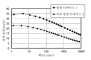
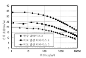
도 13은 발광 디바이스 1 및 비교 발광 디바이스 2의 전류 밀도-휘도 특성을 나타낸 도면이다.
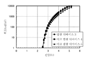
도 14는 발광 디바이스 1 및 비교 발광 디바이스 2의 전압-휘도 특성을 나타낸 도면이다.
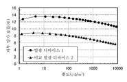
도 15는 발광 디바이스 1 및 비교 발광 디바이스 2의 휘도-전류 효율 특성을 나타낸 도면이다.
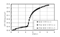
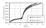
도 16은 발광 디바이스 1 및 비교 발광 디바이스 2의 전압-전류 밀도 특성을 나타낸 도면이다.
도 17은 발광 디바이스 1 및 비교 발광 디바이스 2의 휘도-전력 효율 특성을 나타낸 도면이다.
도 18은 발광 디바이스 1 및 비교 발광 디바이스 2의 휘도-외부 양자 효율 특성을 나타낸 도면이다.
도 19는 발광 디바이스 1 및 비교 발광 디바이스 2의 전계 발광 스펙트럼을 나타낸 도면이다.
도 20은 2TMS-mmtBuDPhA2Anth 및 [Ir(dmdppr-dmp)2(dpm)]의 용액 중의 자외·가시 흡수 스펙트럼 및 발광 스펙트럼이다.
도 21은 발광 디바이스 3, 비교 발광 디바이스 4, 및 비교 발광 디바이스 5의 전류 밀도-휘도 특성을 나타낸 도면이다.
도 22는 발광 디바이스 3, 비교 발광 디바이스 4, 및 비교 발광 디바이스 5의 전압-휘도 특성을 나타낸 도면이다.
도 23은 발광 디바이스 3, 비교 발광 디바이스 4, 및 비교 발광 디바이스 5의 휘도-전류 효율 특성을 나타낸 도면이다.
도 24는 발광 디바이스 3, 비교 발광 디바이스 4, 및 비교 발광 디바이스 5의 전압-전류 밀도 특성을 나타낸 도면이다.
도 25는 발광 디바이스 3, 비교 발광 디바이스 4, 및 비교 발광 디바이스 5의 휘도-전력 효율 특성을 나타낸 도면이다.
도 26은 발광 디바이스 3, 비교 발광 디바이스 4, 및 비교 발광 디바이스 5의 휘도-외부 양자 효율 특성을 나타낸 도면이다.
도 27은 발광 디바이스 3, 비교 발광 디바이스 4, 및 비교 발광 디바이스 5의 전계 발광 스펙트럼을 나타낸 도면이다.
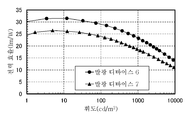
도 28은 발광 디바이스 6 및 발광 디바이스 7의 전류 밀도-휘도 특성을 나타낸 도면이다.
도 29는 발광 디바이스 6 및 발광 디바이스 7의 전압-휘도 특성을 나타낸 도면이다.
도 30은 발광 디바이스 6 및 발광 디바이스 7의 휘도-전류 효율 특성을 나타낸 도면이다.
도 31은 발광 디바이스 6 및 발광 디바이스 7의 전압-전류 밀도 특성을 나타낸 도면이다.
도 32는 발광 디바이스 6 및 발광 디바이스 7의 휘도-전력 효율 특성을 나타낸 도면이다.
도 33은 발광 디바이스 6 및 발광 디바이스 7의 휘도-외부 양자 효율 특성을 나타낸 도면이다.
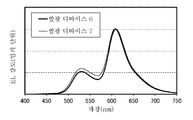
도 34는 발광 디바이스 6 및 발광 디바이스 7의 전계 발광 스펙트럼을 나타낸 도면이다.1A is a diagram showing the structure of a light emitting device. Fig. 1B is a diagram for explaining a light emitting layer.
2 is a conceptual diagram of energy transfer between a host material and a guest material in a light emitting layer.
3A is a conceptual diagram of energy transfer between a general guest material and a host material. 3B is a conceptual diagram of energy transfer between a guest material and a host material used in the light emitting layer.
4A is a structural formula of a guest material used for a light emitting layer. Fig. 4B is a ball-and-stick model of the guest material used for the light emitting layer.
5A and 5B are diagrams for explaining the structure of a light emitting device.
6A, 6B, and 6C are diagrams for explaining a light emitting device.
Fig. 7A is a top view for explaining a light emitting device. Fig. 7B is a cross-sectional view for explaining the light emitting device.
Fig. 8A is a diagram for explaining a mobile computer. Fig. 8B is a diagram for explaining a portable image reproducing apparatus. Fig. 8C is a diagram for explaining a digital camera. Fig. 8D is a diagram for explaining the portable information terminal. Fig. 8E is a diagram for explaining the portable information terminal. Fig. 8F is a diagram for explaining a television device. Fig. 8G is a diagram for explaining the portable information terminal.
9A, 9B, and 9C are diagrams for explaining a foldable portable information terminal.
10A and 10B are diagrams for explaining an automobile.
11A and 11B are diagrams for explaining a lighting device.
It is a figure explaining a light emitting device.
13 is a diagram showing current density-luminance characteristics of light emitting
14 is a diagram showing voltage-luminance characteristics of light emitting
15 is a diagram showing luminance-current efficiency characteristics of light emitting
16 is a diagram showing voltage-current density characteristics of light emitting
17 is a diagram showing luminance-power efficiency characteristics of light emitting
18 is a diagram showing luminance-external quantum efficiency characteristics of light emitting
19 is a diagram showing electroluminescence spectra of light emitting
20 is an ultraviolet and visible absorption spectrum and an emission spectrum in a solution of 2TMS-mmtBuDPhA2Anth and [Ir(dmdppr-dmp) 2 (dpm)].
21 is a diagram showing current density-luminance characteristics of light emitting
22 is a diagram showing voltage-luminance characteristics of light emitting
23 is a diagram showing luminance-current efficiency characteristics of light emitting
24 is a diagram showing voltage-current density characteristics of light emitting
25 is a diagram showing luminance-power efficiency characteristics of light emitting
26 is a diagram showing luminance-external quantum efficiency characteristics of light emitting
27 is a diagram showing electroluminescence spectra of light emitting
28 is a diagram showing the current density-luminance characteristics of the
29 is a diagram showing voltage-luminance characteristics of the
30 is a diagram showing the luminance-current efficiency characteristics of the light-emitting
31 is a diagram showing voltage-current density characteristics of light emitting
32 is a diagram showing the luminance-power efficiency characteristics of the
33 is a diagram showing the luminance-external quantum efficiency characteristics of the light-emitting
34 is a diagram showing the electroluminescence spectra of the
이하에서, 본 발명의 실시형태에 대해서 도면을 사용하여 자세히 설명한다. 다만 본 발명은 이하의 설명에 한정되지 않고, 본 발명의 취지 및 그 범위에서 벗어나지 않고 그 형태 및 자세한 사항을 다양하게 변경할 수 있다. 따라서 본 발명은 이하에 나타내는 실시형태의 기재 내용에 한정하여 해석되는 것은 아니다.EMBODIMENT OF THE INVENTION Hereinafter, embodiment of this invention is described in detail using drawing. However, the present invention is not limited to the following description, and various changes can be made in form and details without departing from the spirit and scope of the present invention. Therefore, this invention is limited to the description of embodiment shown below and is not interpreted.
또한 도면 등에 나타낸 각 구성의 위치, 크기, 범위 등은 이해하기 쉽게 하기 위하여 실제의 위치, 크기, 범위 등을 나타내지 않은 경우가 있다. 따라서 개시(開示)하는 발명은 도면 등에 나타낸 위치, 크기, 범위 등에 반드시 한정되는 것은 아니다.In addition, the actual position, size, range, etc. of each component shown in the drawings and the like may not be shown in order to facilitate understanding. Therefore, the disclosed invention is not necessarily limited to the position, size, range, etc. shown in the drawings.
또한 본 명세서 등에서 도면을 사용하여 발명의 구성을 설명하는 데 있어서, 같은 것을 가리키는 부호는 상이한 도면 간에서도 공통적으로 사용한다.In addition, in this specification, etc., in describing the structure of an invention using drawings, the code|symbol indicating the same is commonly used between different drawings.
또한, 본 명세서 등에서, 단일항 들뜬 상태(S*)는 들뜬 에너지를 가지는 단일항 상태를 의미한다. 또한, S1 준위는 단일항 들뜬 에너지 준위의 가장 낮은 준위이고, 가장 낮은 단일항 들뜬 상태(S1 상태)의 들뜬 에너지 준위를 의미한다. 또한, 삼중항 들뜬 상태(T*)는 들뜬 에너지를 가지는 삼중항 상태를 의미한다. 또한, T1 준위는 삼중항 들뜬 에너지 준위의 가장 낮은 준위이고, 가장 낮은 삼중항 들뜬 상태(T1 상태)의 들뜬 에너지 준위를 의미한다. 또한, 본 명세서 등에서, 단순히 단일항 들뜬 상태 및 단일항 들뜬 에너지 준위라고 표기한 경우에도, S1 상태 및 S1 준위를 나타내는 경우가 있다. 또한, 삼중항 들뜬 상태 및 삼중항 들뜬 에너지 준위라고 표기한 경우에도, T1 상태 및 T1 준위를 나타내는 경우가 있다.In addition, in this specification and the like, the singlet excited state (S * ) refers to a singlet state having an excited energy. In addition, the S1 level is the lowest level of the singlet excited energy level, and means the excited energy level of the lowest singlet excited state (S1 state). In addition, the triplet excited state (T * ) refers to a triplet state having excited energy. In addition, the T1 level is the lowest level of the triplet excited energy level, and means the excited energy level of the lowest triplet excited state (T1 state). In addition, in this specification and the like, even when simply expressed as a singlet excited state and a singlet excited energy level, the S1 state and the S1 level may be indicated in some cases. In addition, even when expressed as a triplet excited state and a triplet excited energy level, a T1 state and a T1 level may be represented.
또한, 본 명세서 등에서 형광 발광 물질이란, 단일항 들뜬 상태로부터 바닥 상태로 완화될 때 가시광 영역 또는 근적외 영역에 발광을 나타내는 화합물이다. 인광 발광 물질이란, 삼중항 들뜬 상태로부터 바닥 상태로 완화될 때 실온에 있어서 가시광 영역 또는 근적외 영역에 발광을 나타내는 화합물이다. 환언하면, 인광 발광 물질이란 삼중항 들뜬 에너지를 발광으로 변환할 수 있는 화합물 중 하나이다.In addition, in this specification and the like, a fluorescent substance is a compound that exhibits light emission in a visible light region or a near-infrared region when relaxed from a singlet excited state to a ground state. A phosphorescent light emitting substance is a compound which exhibits light emission in a visible region or a near-infrared region in room temperature when it relaxes from a triplet excited state to a ground state. In other words, a phosphorescent light-emitting material is one of compounds capable of converting triplet excited energy into light emission.
(실시형태 1)(Embodiment 1)
본 실시형태에서는, 본 발명의 일 형태인 발광 디바이스에 대하여 설명한다. 또한, 발광 디바이스는 도 1의 (A)에 도시된 바와 같이, 제 1 전극(101)(도 1의 (A)에서는 양극인 경우를 나타냄) 및 제 2 전극(102)(도 1의 (A)에서는 음극인 경우를 나타냄)으로 이루어지는 한 쌍의 전극 사이에 EL층(103)이 끼워진 구조를 가지고, EL층(103)은 적어도 발광층(113)을 가지고, 그 외에 정공(홀) 주입층(111), 정공(홀) 수송층(112), 전자 수송층(114), 전자 주입층(115) 등의 기능층을 제공할 수 있다.In this embodiment, a light emitting device as one embodiment of the present invention will be described. In addition, as shown in Fig. 1(A), the light emitting device includes a first electrode 101 (in Fig. 1(A), an anode is shown) and a second electrode 102 (Fig. 1(A)). ) has a structure in which the
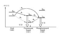
발광층(113)은 발광 물질(게스트 재료)을 포함하는 층이고, 이 외에 호스트 재료를 가지는 것이 바람직하다. 또한, 본 발명의 일 형태에서의 발광 디바이스의 발광층(113)은 호스트 재료로서 기능하는 유기 화합물과 복수의 발광 물질(게스트 재료)을 가지고, 구체적으로는 도 1의 (B)에 도시된 바와 같이, 단일항 들뜬 에너지를 발광으로 변환하는 기능을 가지는 제 1 유기 화합물(121) 및 삼중항 들뜬 에너지를 발광으로 변환하는 기능을 가지는 제 2 유기 화합물(122)을 적어도 가진다. 또한, 호스트 재료로서 기능하는 제 3 유기 화합물(123)을 가진다. 또한, 발광층(113)에서 호스트 재료로서 기능하는 유기 화합물은 복수이어도 좋다.The
발광 디바이스의 발광은 발광층(113)에서 캐리어(정공 및 전자)의 재결합에 의하여 생성된 들뜬 상태의 호스트 재료(복수의 호스트 재료가 들뜬 복합체를 형성하는 경우도 형성하지 않는 경우도 포함함)로부터 게스트 재료로의 에너지 이동이 일어나, 게스트 재료가 발광함으로써 얻어진다.The light emission of the light emitting device is emitted from a host material in an excited state (including cases in which a plurality of host materials form an exciplex) generated by recombination of carriers (holes and electrons) in the
또한, 본 발명의 일 형태인 발광 디바이스는 호스트 재료로서 기능하는 제 3 유기 화합물(123)의 들뜬 상태로부터 단일항 들뜬 에너지를 발광으로 변환하는 기능을 가지는 제 1 유기 화합물(형광 발광 물질인 게스트 재료)(121)로의 에너지 이동, 및 삼중항 들뜬 에너지를 발광으로 변환하는 기능을 가지는 제 2 유기 화합물(인광 발광 물질인 게스트 재료)(122)로의 에너지 이동 양쪽이 발생함으로써, 제 1 유기 화합물(121)로부터의 형광 발광 및 제 2 유기 화합물(122)로부터의 인광 발광이 얻어지는 구성을 가진다. 또한, 제 2 유기 화합물(122)로서 인광 발광 물질 대신에 TADF 재료를 사용할 수 있기 때문에, 인광 발광 물질을 TADF 재료로, 인광 발광을 형광 발광으로 바꿔 읽을 수 있다.In addition, the light emitting device of one embodiment of the present invention provides a first organic compound having a function of converting singlet excited energy from the excited state of the third
본 발명의 일 형태인 발광 디바이스와 같이, 호스트 재료로서 기능하는 제 3 유기 화합물(123)의 들뜬 상태로부터의 에너지 이동에 의하여, 게스트 재료인 제 1 유기 화합물(121)로부터의 형광 발광 및 게스트 재료인 제 2 유기 화합물(122)로부터의 인광 발광 양쪽이 얻어지는 구성으로 하기 위해서는, 도 2에 나타낸 바와 같이, 호스트 재료로서 기능하는 제 3 유기 화합물(123)의 최저 단일항 들뜬 에너지 준위(S1 준위)가 단일항 들뜬 에너지를 발광으로 변환하는 기능을 가지는 제 1 유기 화합물(121)의 S1 준위보다 높다는 관계에 있고, 호스트 재료 및 인광 발광 물질의 T1 준위로부터 형광 발광 물질의 T1 준위로의 에너지 이동이 쉽게 일어나지 않아야 한다.As in the light emitting device of one embodiment of the present invention, by energy transfer from the excited state of the third
도 2에는 본 발명의 일 형태인 발광 디바이스의 발광층(113)에서의 에너지(Energy) 준위의 상관의 일례를 나타내었다. 또한, 도 2에서는 도 1의 (B)와 공통되는 부호를 사용하는 것으로 하지만, 편의상 호스트 재료로서 기능하는 제 3 유기 화합물(123)을 Host(123)로, 단일항 들뜬 에너지를 발광으로 변환하는 기능을 가지는 제 1 유기 화합물(121)을 Fluorecent Guest(121)로, 삼중항 들뜬 에너지를 발광으로 변환하는 기능을 가지는 제 2 유기 화합물(122)을 Phosphorecent Guest(122)로 나타내었다. 그 외의 표기 및 부호는 다음과 같다.FIG. 2 shows an example of the correlation of energy levels in the
·SH1: 제 3 유기 화합물(123)의 S1 준위·S H1 : S1 level of the third organic compound (123)
·TH1: 제 3 유기 화합물(123)의 T1 준위· T H1 : T1 level of the third organic compound (123)
·SFG: 제 1 유기 화합물(121)의 S1 준위·S FG : S1 level of the first
·TFG: 제 1 유기 화합물(121)의 T1 준위T FG : T1 level of the first
·SPG: 제 2 유기 화합물(122)의 T1 준위·S PG : T1 level of the second organic compound (122)
·TPG: 제 2 유기 화합물(122)의 T1 준위T PG : T1 level of the second
제 3 유기 화합물(123)이 들뜬 상태가 되면, 단일항 들뜬 에너지는 신속히 제 1 유기 화합물(121)로 이동할 수 있다(도 2의 경로 A1). 이때, SH1≥SFG인 것이 바람직하다. 구체적으로는, 제 3 유기 화합물(123)의 형광 스펙트럼의 단파장 측의 꼬리에 접선을 긋고, 그 외삽선의 파장의 에너지를 SH1로 하고, 제 1 유기 화합물(121)의 흡수 스펙트럼의 흡수단의 파장의 에너지를 SFG로 하였을 때, SH1≥SFG인 것이 바람직하다.When the third
또한, 제 2 유기 화합물(122)은 인광 발광 물질이기 때문에 제 3 유기 화합물(123)이 가지는 단일항 들뜬 에너지 및 삼중항 들뜬 에너지를 받을 수 있다(도 2의 경로 A2). 이때, TH1≥TPG인 것이 바람직하다. 또한, 제 2 유기 화합물(122)의 흡수 스펙트럼의 흡수단의 파장의 에너지를 TPG로 간주할 수 있다. 또한, 제 3 유기 화합물(123)의 저온(예를 들어 10K)에서의 발광 스펙트럼의 단파장 측의 발광 단부의 파장 에너지를 TH1로 간주할 수 있다. 또한, 제 1 유기 화합물(121) 및 제 2 유기 화합물(122)의 발광 양쪽을 양호한 비율로 얻기 위해서는 SFG≥TPG인 것이 바람직하다.Also, since the second
발광층(113)에서, 제 3 유기 화합물(123), 제 1 유기 화합물(121), 및 제 2 유기 화합물(122)은 혼합되어 있다. 그러므로, 제 3 유기 화합물(123)과 제 1 유기 화합물(121) 사이에서는 경로 A1과 경합되어 제 3 유기 화합물(123)의 삼중항 들뜬 에너지가 제 1 유기 화합물(121)의 삼중항 들뜬 에너지로 변환되는 과정(도 2의 경로 A3)이 일어날 수 있다. 제 1 유기 화합물(121)은 형광 발광 물질이기 때문에 제 1 유기 화합물(121)의 삼중항 들뜬 에너지는 발광에 기여하지 않는다. 즉, 경로 A3의 에너지 이동이 생기면 발광 디바이스의 발광 효율이 저하된다. 또한 실제로는 TH1로부터 TFG로의 에너지 이동 과정 A3은 직접적인 것이 아니라, 제 1 유기 화합물(121)의 TFG보다 높은 준위의 삼중항 들뜬 상태로 한번 에너지 이동하고, 그 후 내부 변환에 의하여 TFG가 되는 경로가 있을 수 있지만, 도면 중에서는 그 과정을 생략하여 나타내었다. 이후 본 명세서 중에서의 바람직하지 않은 열 비활성화 과정, 즉 TFG로의 비활성화 과정은 모두 마찬가지이다.In the
또한, 도 2에 나타낸 바와 같이, SFG≥TPG인 경우, 제 1 유기 화합물(121)이 가지는 단일항 들뜬 에너지는 형광 발광으로 변환되는 과정과, TPG로 에너지 이동하는 과정(도 2의 경로 A4)이 경합한다. 즉, 제 2 유기 화합물(122)이 들뜬 에너지를 받는 경로로서는 경로 A2 및 A4가 존재한다. 그러므로, 제 1 유기 화합물(121) 및 제 2 유기 화합물(122)의 발광 양쪽을 양호한 비율로 얻기 위해서는, 발광층(113)에서의 제 1 유기 화합물(121)의 농도가 제 2 유기 화합물(122)의 농도보다 높은 것이 바람직하다. 또한, 발광층(113)에서의 제 2 유기 화합물(122)의 농도가 낮으면 제 2 유기 화합물(122)에서 캐리어가 재결합되기 어려워지므로 바람직하다.In addition, as shown in FIG. 2 , when S FG ≥ T PG , the singlet excited energy of the first
또한, 제 2 유기 화합물(122)이 가지는 삼중항 들뜬 에너지는 발광으로 변환되는 과정과, 제 2 유기 화합물(122)의 삼중항 들뜬 에너지가 제 1 유기 화합물(121)의 삼중항 들뜬 에너지로 변환되는 과정(도 2의 경로 A5)이 경합되어 일어날 수 있다. 제 1 유기 화합물(121)은 형광 발광 물질이기 때문에 제 1 유기 화합물(121)의 삼중항 들뜬 에너지는 발광에 기여하지 않는다. 즉, 경로 A5의 에너지 이동이 생기면 발광 디바이스의 발광 효율이 저하한다.In addition, the triplet excited energy of the second
또한, 화합물의 발광 파장이 단파장일수록 높은 에너지로 여기된다. 그러므로, 발광 디바이스에 있어서 양호한 신뢰성을 얻기 위해서는, 단파장의 발광을 나타내는 화합물에 발광 속도 상수가 높은 발광 물질을 사용하는 것이 바람직하고, 형광 발광 물질을 사용하는 것이 바람직하다. 환언하면, 제 2 유기 화합물(122)이 나타내는 발광 스펙트럼은 제 1 유기 화합물(121)이 나타내는 발광 스펙트럼의 피크 파장보다 장파장에 발광 피크를 가지는 것이 바람직하다.In addition, the shorter the emission wavelength of the compound, the higher the energy is excited. Therefore, in order to obtain good reliability in a light emitting device, it is preferable to use a light emitting material having a high light emission rate constant for a compound exhibiting light emission of a short wavelength, and it is preferable to use a fluorescent light emitting material. In other words, the emission spectrum of the second
일반적으로, 분자 간의 에너지 이동 기구로서, 푀르스터 기구(쌍극자-쌍극자 상호 작용)와 덱스터 기구(전자 교환 상호 작용)가 알려져 있다. 에너지 억셉터인 제 1 유기 화합물(121)은 형광 발광 물질이기 때문에 경로 A3 및 경로 A5의 에너지 이동은 덱스터 기구가 지배적이다. 일반적으로, 덱스터 기구는 에너지 도너인 제 3 유기 화합물(123)과 에너지 억셉터인 제 1 유기 화합물(121)의 거리가 1nm 이하에서 유의하게 생긴다. 또한, 제 1 유기 화합물(121)과 제 2 유기 화합물(122)의 거리가 1nm 이하인 경우에도 덱스터 기구는 유의하게 생긴다. 그러므로, 경로 A3 및 경로 A5를 억제하기 위해서는, 에너지 도너와 에너지 억셉터의 거리를 떨어지게 하는 것이 중요하다.In general, as an energy transfer mechanism between molecules, a Förster mechanism (dipole-dipole interaction) and a Dexter mechanism (electron exchange interaction) are known. Since the first
또한, 제 3 유기 화합물(123)의 단일항 들뜬 에너지 준위(SH1)로부터 제 1 유기 화합물(121)의 삼중항 들뜬 에너지 준위(TFG)로의 에너지 이동은 제 1 유기 화합물(121)에서의 단일항 바닥 상태로부터 삼중항 들뜬 상태로의 직접 전이가 금제이므로, 주된 에너지 이동 과정이 되기 어렵기 때문에 도시하지 않았다.In addition, the energy transfer from the singlet excited energy level (S H1 ) of the third
도 2 중의 TFG는 제 1 유기 화합물(121)인 형광 발광 물질의 발광단에서 유래되는 에너지 준위인 경우가 많다. 그러므로, 경로 A3 및 경로 A5의 에너지 이동을 억제하기 위해서는, 에너지 도너가 되는 제 3 유기 화합물(123)이나 제 2 유기 화합물(122)과 에너지 억셉터가 되는 제 1 유기 화합물(121)이 가지는 발광단의 거리를 떨어지게 함으로써, 덱스터 기구에 의한 에너지 이동을 억제하는 것이 중요하다. In many cases, T FG in FIG. 2 is an energy level derived from the light emitting end of the fluorescent material, which is the first
에너지 도너와 에너지 억셉터가 되는 제 1 유기 화합물(121)이 가지는 발광단의 거리를 떨어지게 하기 위한 방법으로서는, 일반적으로 이들 유기 화합물의 혼합막 내에서의 제 1 유기 화합물(121)의 농도를 낮추는 방법을 들 수 있다. 그러나, 혼합막 내에서의 제 1 유기 화합물(121)의 농도를 낮추면, 에너지 도너로부터 에너지 억셉터가 되는 제 1 유기 화합물(121)이 가지는 발광단으로의 덱스터 기구에 의거한 에너지 이동뿐만 아니라, 푀르스터 기구에 의거한 에너지 이동도 억제된다. 그 경우, 경로 A1이 푀르스터 기구에 의거하기 때문에, 발광 디바이스의 발광 효율의 저하나 신뢰성의 저하와 같은 문제가 생긴다.As a method for reducing the distance between the light emitting end of the first
본 발명자들은 에너지 억셉터인 제 1 유기 화합물(121)과 에너지 도너인 제 3 유기 화합물(123) 및 제 2 유기 화합물(122)의 거리를 떨어지게 하기 위하여, 에너지 억셉터인 제 1 유기 화합물(121)로서 보호기를 가지는 형광 발광 물질을 사용함으로써, 상술한 에너지 이동에 따른 발광 효율의 저하를 억제할 수 있는 것을 발견하였다. 또한, 상기 보호기를 가지는 제 1 유기 화합물(121)을 사용함으로써, 제 1 유기 화합물(121)과 제 2 유기 화합물(122)을 가지는 발광층(113)으로부터, 제 1 유기 화합물(121)에서 유래되는 발광(형광 발광)과 제 2 유기 화합물(122)에서 유래되는 발광(인광 발광 또는 형광 발광) 양쪽이 얻어지는 것을 발견하였다.In order to separate the first
다음으로, 본 발명의 일 형태인 발광 디바이스의 발광층에서의 호스트 재료와 게스트 재료 사이의 에너지 이동의 개념에 대하여 도 3의 (A), (B)를 사용하여 설명한다.Next, the concept of energy transfer between the host material and the guest material in the light emitting layer of the light emitting device of one embodiment of the present invention will be described with reference to Figs. 3A and 3B.
도 3의 (A)는 호스트 재료인 제 3 유기 화합물(123)과 게스트 재료인 형광 발광 물질(124)이 존재하는 상황을 나타낸 것이다. 또한, 형광 발광 물질(124)은 일반적인 형광 발광 물질이고, 발광단(130a)을 가지지만 보호기를 가지지 않는 형광 발광 물질이다.3A illustrates a situation in which the third
또한, 도 3의 (B)는 호스트 재료인 제 3 유기 화합물(123)과 게스트 재료인 제 1 유기 화합물(형광 발광 물질)(121)이 존재하는 상황을 나타낸 것이다. 또한, 제 1 유기 화합물(121)은 본 발명의 일 형태인 발광 디바이스에 있어서, 에너지 억셉터로서 사용하는 형광 발광 물질이고, 발광단(130b)과 보호기(131)를 가진다. 또한, 보호기(131)는 제 3 유기 화합물(호스트 재료)(123)로부터 발광단(130b)으로의 덱스터 기구에 의거하여 에너지 이동이 일어나기 어려울 정도의 거리를 두고, 이들을 떨어지게 하는 기능을 가진다.Also, FIG. 3B illustrates a situation in which the third
도 3의 (A), (B)에 도시된 바와 같이, 발광층에 있어서, 호스트 재료인 제 3 유기 화합물(123), 게스트 재료인 형광 발광 물질(124), 또는 제 1 유기 화합물(형광 발광 물질)(121)은 서로 가까운 위치에 존재한다. 그러므로, 도 3의 (A)에 도시된 바와 같이, 형광 발광 물질(124)이 보호기를 가지지 않는 경우에는, 발광단(130a)과 제 3 유기 화합물(123)의 거리가 가까워지기 때문에, 제 3 유기 화합물(123)로부터 형광 발광 물질(124)로의 에너지 이동으로서, 푀르스터 기구에 의한 에너지 이동(도 3의 (A)의 경로 A6)과 덱스터 기구에 의한 에너지 이동(도 3의 (A)의 경로 A7) 양쪽이 생길 수 있다. 덱스터 기구에 의한 호스트 재료로부터 게스트 재료로의 삼중항 들뜬 에너지의 에너지 이동이 생기고, 게스트 재료의 삼중항 들뜬 상태가 생성되어도 게스트 재료가 형광 발광 물질인 경우에는, 삼중항 들뜬 에너지가 비복사성 비활성화되기 때문에, 발광 디바이스의 발광 효율 저하의 원인 중 하나가 된다.3A and 3B, in the light emitting layer, a third
한편, 도 3의 (B)에서는 게스트 재료인 제 1 유기 화합물(형광 발광 물질)(121)이 보호기(131)를 가지기 때문에, 발광단(130b)과 호스트 재료인 제 3 유기 화합물(123)의 거리를 떨어지게 할 수 있다. 이로써, 덱스터 기구에 의한 에너지 이동(경로 A7)을 억제할 수 있다. 그러므로, 본 발명의 일 형태인 발광 디바이스의 발광층에 있어서, 게스트 재료로서 보호기(131)를 가지는 제 1 유기 화합물(형광 발광 물질)(121)을 사용함으로써, 발광층 내에 존재하는 호스트 재료(제 3 유기 화합물(123))로부터 제 1 유기 화합물(121)로의 에너지 이동(도 2의 경로 A3)을 억제할 수 있다. 또한, 발광층 내에 존재하는 다른 게스트 재료(도 2에서 설명한 제 2 유기 화합물(122))에 대해서도 마찬가지로, 제 2 유기 화합물(122)로부터 제 1 유기 화합물(121)로의 에너지 이동(도 2의 경로 A3)을 억제할 수 있다.On the other hand, in FIG. 3B , since the first organic compound (fluorescent light emitting material) 121 as a guest material has a
여기서, 도 3의 (A)에 도시된 형광 발광 물질(124)이 가지는 발광단(130a)이나 도 3의 (B)에 도시된 제 1 유기 화합물(형광 발광 물질)(121)이 가지는 발광단(130b)에 대하여 설명한다. 발광단(130a, 130b)이란, 형광 발광 물질에 있어서, 발광의 원인이 되는 원자단(골격)을 가리킨다. 발광단(130a, 130b)은 일반적으로 π결합을 가지고, 방향족 고리를 포함하는 것이 바람직하고, 축합 방향족 고리 또는 축합 헤테로 방향족 고리를 가지는 것이 바람직하다. 또한, 다른 형태로서, 고리 평면상에 전이 쌍극자 벡터가 존재하는 방향족 고리를 포함하는 원자단(골격)을 발광단(130a, 130b)으로 간주할 수 있다. 또한, 하나의 형광 발광 물질이 복수의 축합 방향족 고리 또는 축합 헤테로 방향족 고리를 가지는 경우에는, 상기 복수의 축합 방향족 고리 또는 축합 헤테로 방향족 고리 중, 가장 낮은 S1 준위를 가지는 골격을 상기 형광 발광 물질의 발광단으로 간주하는 경우도 있다. 또한, 상기 복수의 축합 고리 또는 축합 헤테로 방향족 고리를 가지는 경우, 가장 장파장 측에 흡수단을 가지는 골격을 상기 형광 발광 물질의 발광단으로 간주하는 경우도 있다. 또한, 상기 복수의 축합 고리 또는 축합 헤테로 방향족 고리를 가지는 경우, 각각의 발광 스펙트럼의 형상으로부터 상기 형광 발광 물질의 발광단을 예상할 수 있는 경우가 있다.Here, the
상기 축합 방향족 고리 또는 축합 헤테로 방향족 고리로서는, 페난트렌 골격, 스틸벤 골격, 아크리돈 골격, 페녹사진 골격, 페노싸이아진 골격 등을 들 수 있다. 특히, 나프탈렌 골격, 안트라센 골격, 플루오렌 골격, 크리센 골격, 트라이페닐렌 골격, 테트라센 골격, 피렌 골격, 페릴렌 골격, 쿠마린 골격, 퀴나크리돈 골격, 나프토비스벤조퓨란 골격을 가지는 형광 발광 물질은 형광 양자 수율이 높기 때문에 바람직하다.Examples of the condensed aromatic ring or the condensed heteroaromatic ring include a phenanthrene skeleton, a stilbene skeleton, an acridone skeleton, a phenoxazine skeleton, and a phenothiazine skeleton. In particular, a fluorescent substance having a naphthalene skeleton, an anthracene skeleton, a fluorene skeleton, a chrysene skeleton, a triphenylene skeleton, a tetracene skeleton, a pyrene skeleton, a perylene skeleton, a coumarin skeleton, a quinacridone skeleton, or a naphthobisbenzofuran skeleton Silver is preferred because of its high fluorescence quantum yield.
또한, 도 3의 (B)에 도시된 제 1 유기 화합물(형광 발광 물질)(121)이 가지는 보호기(131)로서는, 발광단(130b) 및 호스트 재료인 제 3 유기 화합물(123)이 가지는 T1 준위보다 높은 T1 준위를 가지는 것이 바람직하다. 따라서, 포화 탄화수소기를 보호기로서 적합하게 사용할 수 있다. 포화 탄화수소기는, π결합을 가지지 않기 때문에 T1 준위가 높고, 캐리어(전자 또는 정공)를 수송하는 기능이 낮다. 그러므로, 제 1 유기 화합물(121)이 보호기(131)로서 포화 탄화수소기를 가짐으로써, 호스트 재료인 제 3 유기 화합물(123)의 들뜬 상태나 캐리어 수송성에 거의 영향을 미치지 않고, 발광단(130b) 및 호스트 재료인 제 3 유기 화합물(123)의 거리를 떨어지게 할 수 있다.In addition, as the
또한, 제 1 유기 화합물(형광 발광 물질)(121)이 π결합을 가지지 않는 치환기와 π공액을 가지는 치환기를 동시에 가지는 경우는, π공액을 가지는 치환기 측에 프런티어 궤도{HOMO(Highest Occupied Molecular Orbital, 최고 점유 분자 궤도라고도 함) 및 LUMO(Lowest Unoccupied Molecular Orbital, 최저 비점유 분자 궤도라고도 함)}가 존재하는 경우가 많고, 특히 발광단(130b)이 프런티어 궤도를 가지는 경우가 많다. 후술하는 바와 같이, 덱스터 기구에 의한 에너지 이동에는 에너지 도너 및 에너지 억셉터 양쪽의 HOMO의 중첩과 양쪽의 LUMO의 중첩이 중요하다. 그러므로, 포화 탄화수소기를 보호기에 사용함으로써, 에너지 도너인 제 3 유기 화합물(123)의 프런티어 궤도와 에너지 억셉터인 제 1 유기 화합물(121)의 프런티어 궤도의 거리를 떨어지게 할 수 있어 덱스터 기구에 의한 에너지 이동을 억제할 수 있다.Further, when the first organic compound (fluorescent light emitting material) 121 has a substituent having no π bond and a substituent having π conjugated at the same time, a frontier orbital {HOMO (Highest Occupied Molecular Orbital, Most often, the
또한, 보호기(131)의 구체적인 예로서는, 탄소수 1 이상 10 이하의 알킬기를 들 수 있다. 또한, 보호기(131)는 게스트 재료인 제 1 유기 화합물(121)의 발광단(130b)과 호스트 재료인 제 3 유기 화합물(123)의 거리를 떨어지게 할 필요가 있기 때문에, 부피가 큰 구조를 가지는 것이 바람직하다. 그러므로, 탄소수 3 이상 10 이하의 알킬기, 치환 또는 비치환된 탄소수 3 이상 10 이하의 사이클로알킬기, 탄소수 3 이상 10 이하의 트라이알킬실릴기를 적합하게 사용할 수 있다. 특히 알킬기로서는, 부피가 큰 분지쇄 알킬기가 바람직하다. 또한, 상기 치환기는 4급 탄소를 가지면 부피가 큰 치환기가 되기 때문에 특히 바람직하다.In addition, as a specific example of the
또한, 보호기(131)는 하나의 발광단(130b)에 대하여 5개 이상 가지는 것이 바람직하다. 상기 구조로 함으로써, 발광단(130b) 전체를 보호기(131)로 덮을 수 있기 때문에, 제 3 유기 화합물(123)과 발광단의 거리를 적절히 조정할 수 있다. 또한, 보호기(131)는 발광단(130b)과 직접 결합되지 않는 것이 더 바람직하다. 예를 들어, 아릴렌기나 아미노기 등의 2가 이상의 치환기를 개재하여, 보호기(131)와 발광단(130b)이 결합되는 것이 좋다. 상기 치환기를 개재하여 보호기(131)와 발광단(130b)을 결합시킴으로써, 발광단(130b)과 제 3 유기 화합물(123)의 거리를 효과적으로 떨어지게 할 수 있다. 또한, 상기 치환기를 개재하여 보호기(131)와 발광단(130b)을 결합시키는 경우, 하나의 발광단에 대하여 보호기를 4개 이상 가지면, 덱스터 기구를 효과적으로 억제할 수 있어 바람직하다.In addition, it is preferable to have five or more protecting
또한, 발광단(130b)과 보호기(131)를 결합시키는 2가 이상의 치환기는 π공액을 가지는 치환기인 것이 바람직하다. 상기 구성으로 함으로써, 게스트 재료인 제 1 유기 화합물(121)의 발광색이나 HOMO 준위, 유리 전이점 등의 물성을 조정할 수 있다. 또한, 발광단을 중심으로 분자 구조를 보았을 때, 보호기(131)는 가장 외측에 배치되는 것이 바람직하다.In addition, it is preferable that the substituent having a divalent or higher valence bonding the
상술한 바와 같이, 제 1 유기 화합물(121)은 덱스터 기구에 의한 에너지 이동이 억제되어 있기 때문에, 제 1 유기 화합물(121)이 발광하기 위해서는 제 3 유기 화합물(123)로부터 푀르스터 기구에 의하여 에너지를 받을 필요가 있다. 즉, 덱스터 기구에 의한 에너지 이동은 억제하면서, 푀르스터 기구에 의한 에너지 이동을 효율적으로 이용하는 것이 바람직하다. 푀르스터 기구에 의한 에너지 이동도 호스트 재료와 게스트 재료의 거리로 인하여 영향을 받는 것이 알려져 있다. 일반적으로, 호스트 재료와 게스트 재료의 거리가 1nm 이하인 경우에 덱스터 기구가 우세가 되고, 1nm 이상 10nm 이하의 경우에는 푀르스터 기구가 우세가 된다. 다만, 호스트 재료와 게스트 재료의 거리의 거리가 10nm 이상이면 에너지 이동은 생기기 어렵다는 것이 알려져 있다.As described above, since energy transfer by the Dexter mechanism is suppressed in the first
또한, 본 명세서 중에 있어서, 상술한 호스트 재료인 제 3 유기 화합물(123)과 게스트 재료인 제 1 유기 화합물(121)의 거리는 제 3 유기 화합물(123)과 제 1 유기 화합물(121)이 가지는 발광단(130b)의 거리와 동일한 것으로 한다. 따라서, 제 1 유기 화합물(121)이 가지는 보호기(131)가 제 1 유기 화합물(121)이 가지는 발광단(130b)으로부터 1nm 이상 10nm 이하의 범위까지 퍼짐으로써, 푀르스터 기구를 우세로 할 수 있기 때문에 바람직하다. 또한, 제 1 유기 화합물(121)이 가지는 보호기(131)가 퍼지는 범위는 1nm 이상 5nm 이하의 범위로 하는 것이 더 바람직하다. 상기 구성으로 함으로써, 호스트 재료인 제 3 유기 화합물(123)로부터 제 1 유기 화합물(121)로의 덱스터 기구에 의한 에너지 이동을 억제하면서, 푀르스터 기구에 의한 에너지 이동을 효율적으로 수행할 수 있기 때문에, 높은 발광 효율을 가지는 발광 디바이스를 제작할 수 있다.In addition, in the present specification, the distance between the above-described third
일반적으로 푀르스터 기구에 의한 에너지 이동 효율을 높이기 위하여(에너지 이동 속도를 향상시키기 위하여) 호스트 재료에 대한 게스트 재료로서 형광 발광 물질의 농도 비율을 높이는 것이 바람직하지만, 게스트 재료의 농도 비율을 높이면, 덱스터 기구에 의한 에너지 이동의 이동 속도가 향상되고, 결과적으로 발광 효율이 저하한다는 트래이드오프의 관계를 가진다. 따라서, 게스트 재료의 농도 비율을 높이는 것은 발광 효율을 향상시키기 위한 유효한 수단이라고 할 수는 없었다.In general, it is preferable to increase the concentration ratio of the fluorescent light emitting material as the guest material to the host material in order to increase the energy transfer efficiency by the Förster mechanism (to improve the energy transfer speed), but if the concentration ratio of the guest material is increased, Dexter There is a trade-off relationship in that the movement speed of energy transfer by the mechanism is improved and, as a result, the luminous efficiency is lowered. Therefore, increasing the concentration ratio of the guest material cannot be said to be an effective means for improving the luminous efficiency.
이에 대하여, 본 발명의 일 형태인 발광 디바이스에 사용하는 제 1 유기 화합물(121)은 호스트 재료로부터의 덱스터 기구에 의한 에너지 이동을 억제할 수 있는 구조를 가지기 때문에, 발광층에서의 게스트 재료로서 사용하였을 때, 호스트 재료에 대한 농도 비율을 높임으로써 푀르스터 기구에 의한 에너지 이동 효율을 높일(에너지 이동 속도를 향상시킬) 수 있다. 또한, 호스트 재료에 대한 농도 비율을 높이고, 푀르스터 기구에 의한 에너지 이동 속도를 높임으로써, 발광층 내의 게스트 재료(에너지 억셉터)의 여기 수명을 짧게 할 수 있기 때문에, 발광 디바이스의 신뢰성을 향상시킬 수 있다.On the other hand, since the first
또한, 본 발명의 일 형태인 발광 디바이스의 발광층에 있어서, 게스트 재료인 제 1 유기 화합물(121)의 농도는 호스트 재료인 제 3 유기 화합물(123)에 대하여, 2wt% 이상 30wt% 이하가 바람직하고, 더 바람직하게는 5wt% 이상 20wt% 이하, 더 바람직하게는 5wt% 이상 15wt% 이하로 한다. 상기 구성으로 함으로써, 푀르스터 기구에 의한 에너지 이동 속도를 높일 수 있기 때문에, 발광 효율이 높은 발광 디바이스를 얻을 수 있다. 또한, 본 발명의 일 형태인 발광 디바이스의 발광층은 상기 구성에 더하여, 게스트 재료로서 삼중항 들뜬 에너지를 발광으로 변환하는 기능을 가지는 제 2 유기 화합물(122)을 가진다. 따라서, 본 발명의 일 형태인 발광 디바이스는 제 1 유기 화합물(121)로부터 얻어지는 형광 발광과 제 2 유기 화합물(122)로부터 얻어지는 발광(인광 발광 또는 형광 발광) 양쪽을 높은 발광 효율로 얻을 수 있다. 이때, 제 1 유기 화합물(121) 및 제 2 유기 화합물(122)의 발광 양쪽을 양호한 비율로 얻기 위해서는, 발광층(113)에서의 제 1 유기 화합물(121)의 농도가 제 2 유기 화합물(122)의 농도보다 높은 것이 더 바람직하다.In addition, in the light emitting layer of the light emitting device of one embodiment of the present invention, the concentration of the first
발광 디바이스에 있어서, 상술한 에너지 이동은 열화물이나 불순물의 영향으로 인한 소광 과정과 항상 경합한다. 즉, 소광 과정의 소광 속도 상수가 시간 경과에 따라 커지면, 발광 디바이스에서의 발광의 비율이 감소되고, 발광 디바이스의 휘도 열화가 생긴다. 그러나, 상술한 바와 같이, 본 발명의 일 형태인 발광 디바이스는 덱스터 기구에 의한 에너지 이동을 억제하면서, 푀르스터 기구에 의한 에너지 이동 속도를 종래보다 높일 수 있기 때문에, 소광 과정과의 경합의 영향을 작게 하고, 발광 디바이스를 장수명화를 도모할 수 있다.In light emitting devices, the energy transfer described above always competes with the quenching process due to the influence of deterioration or impurities. That is, when the extinction rate constant of the quenching process becomes large with the lapse of time, the ratio of light emission in the light emitting device decreases, and deterioration of the luminance of the light emitting device occurs. However, as described above, in the light emitting device of one embodiment of the present invention, while suppressing the energy transfer by the Dexter mechanism, the energy transfer speed by the Förster mechanism can be increased compared to the prior art, so the effect of competition with the quenching process is reduced. It can be made small, and the lifespan of the light emitting device can be increased.
여기서, 상술한 푀르스터 기구와 덱스터 기구에 대하여 설명한다. 여기서는, 들뜬 상태인 제 1 유기 화합물로부터 바닥 상태인 제 2 유기 화합물로의 들뜬 에너지의 공여에 관하여, 제 1 유기 화합물과 제 2 유기 화합물의 분자 간의 에너지 이동 과정에 대하여 설명하지만, 어느 한쪽이 들뜬 복합체인 경우도 마찬가지이다.Here, the Feuerster mechanism and the Dexter mechanism described above will be described. Here, the energy transfer process between molecules of the first organic compound and the second organic compound will be described with respect to the donation of excited energy from the first organic compound in the excited state to the second organic compound in the ground state. The same is true for complexes.
<<푀르스터 기구>><<Feuerster Organization>>
푀르스터 기구에서는, 에너지 이동에 분자 간의 직접적 접촉이 불필요하고, 제 3 유기 화합물 및 제 1 유기 화합물의 쌍극자 진동의 공명 현상으로 에너지 이동이 일어난다. 쌍극자 진동의 공명 현상에 의하여 제 3 유기 화합물이 제 1 유기 화합물에 에너지를 공여하고, 들뜬 상태의 제 3 유기 화합물이 바닥 상태가 되고, 바닥 상태의 제 1 유기 화합물이 들뜬 상태가 된다. 또한, 푀르스터 기구의 속도 상수 kh*→g를 식(1)에 나타내었다.In the Feuerster mechanism, direct contact between molecules is unnecessary for energy transfer, and energy transfer occurs due to the resonance phenomenon of dipole vibrations of the third organic compound and the first organic compound. By the resonance phenomenon of dipole vibration, the third organic compound donates energy to the first organic compound, and the third organic compound in an excited state becomes a ground state, and the first organic compound in a ground state becomes an excited state. In addition, the rate constant k h*→g of the Feuerster mechanism is shown in Equation (1).
[수학식 1][Equation 1]

식(1)에서, ν는 진동수를 나타내고, f'h(ν)는 제 3 유기 화합물의 정규화된 발광 스펙트럼(단일항 들뜬 상태로부터의 에너지 이동을 논의하는 경우에는 형광 스펙트럼, 삼중항 들뜬 상태로부터의 에너지 이동을 논의하는 경우에는 인광 스펙트럼)을 나타내고, εg(ν)는 제 1 유기 화합물의 몰 흡광 계수 스펙트럼을 나타내고, N은 아보가드로수를 나타내고, n은 매체의 굴절률을 나타내고, R는 제 3 유기 화합물과 제 1 유기 화합물의 분자 간 거리를 나타내고, τ는 실측되는 들뜬 상태의 수명(형광 수명이나 인광 수명)을 나타내고, c는 광속을 나타내고, φ는 발광 양자 수율(단일항 들뜬 상태로부터의 에너지 이동을 논의하는 경우에는 형광 양자 수율, 삼중항 들뜬 상태로부터의 에너지 이동을 논의하는 경우에는 인광 양자 수율)을 나타내고, K2은 제 3 유기 화합물과 제 1 유기 화합물의 전이 쌍극자 모멘트의 배향을 나타내는 계수(0 내지 4)이다. 또한, 랜덤 배향의 경우에는 K2=2/3이다.In equation (1), ν denotes the frequency, and f′ h (ν) is the normalized emission spectrum of the third organic compound (fluorescence spectrum if energy transfer from singlet excited state is discussed, triplet excited state from represents the phosphorescence spectrum when discussing the energy transfer of ), ε g (ν) represents the molar extinction coefficient spectrum of the first organic compound, N represents Avogadro's number, n represents the refractive index of the medium, and R represents the second 3 represents the distance between molecules of the organic compound and the first organic compound, τ represents the measured lifetime of the excited state (fluorescence lifetime or phosphorescence lifetime), c represents the luminous flux, and φ represents the emission quantum yield (from a singlet excited state). represents the fluorescence quantum yield when discussing the energy transfer of , and phosphorescence quantum yield when discussing the energy transfer from the triplet excited state), and K 2 is the orientation of the transition dipole moment of the third organic compound and the first organic compound. is a coefficient (0 to 4) representing Further, in the case of random orientation, K 2 =2/3.
여기서, 에너지 도너를 제 3 유기 화합물로 하고, 에너지 억셉터를 제 1 유기 화합물로 한 경우, 제 3 유기 화합물 및 제 1 유기 화합물의 발광색이 가까우면, 상기 식(1)에 따르면, f'h(ν) 및 εg(ν)의 중첩이 작아지기 때문에(εg(ν)는 제 1 유기 화합물의 발광 스펙트럼보다 장파장 측에 존재하기 때문에), 식(1)에 따르면 kh*→g가 작아진다. 그러나, 본 발명의 일 형태인 발광 디바이스에서는, 상술한 바와 같이 발광층 내에서의 에너지 도너의 농도를 높일 수 있기 때문에, 식(1) 중의 R의 값을 크게 할 수 있어, kh*→g의 저하를 억제할 수 있다. 따라서, 본 발명의 일 형태인 발광 디바이스에서는, 에너지 도너에 가까운 발광색을 가지는 형광 발광 물질을 발광 재료로서 사용할 수 있다. 또한 본 발명의 일 형태의 발광 디바이스는 에너지 도너와 에너지 억셉터의 발광색이 상이하여도 사용할 수 있다.Here, when the energy donor is the third organic compound and the energy acceptor is the first organic compound, if the emission colors of the third organic compound and the first organic compound are close, according to the above formula (1), f' h Since the overlap of (ν) and ε g (ν) becomes small (since ε g (ν) exists on the longer wavelength side than the emission spectrum of the first organic compound), according to Equation (1), k h*→g is gets smaller However, in the light emitting device of one embodiment of the present invention, since the concentration of the energy donor in the light emitting layer can be increased as described above, the value of R in Equation (1) can be increased, so that k h * → g deterioration can be suppressed. Therefore, in the light emitting device of one embodiment of the present invention, a fluorescent material having an emission color close to that of an energy donor can be used as the light emitting material. In addition, the light emitting device of one embodiment of the present invention can be used even if the emission colors of the energy donor and the energy acceptor are different.
<<덱스터 기구>><<Dexter Mechanism>>
덱스터 기구에서는 제 3 유기 화합물과 제 1 유기 화합물이 궤도의 중첩이 생길 접촉 유효 거리까지 가까워지면, 들뜬 상태의 제 3 유기 화합물의 전자와 바닥 상태의 제 1 유기 화합물의 전자의 교환으로 에너지 이동이 일어난다. 또한, 덱스터 기구의 속도 상수 kh*→g를 식(2)에 나타내었다.In the Dexter mechanism, when the third organic compound and the first organic compound come close to the effective contact distance at which the orbital overlap occurs, the energy transfer occurs due to the exchange of electrons of the third organic compound in the excited state and the electrons of the first organic compound in the ground state. happens In addition, the rate constant k h*→g of the Dexter mechanism is shown in Equation (2).
[수학식 2][Equation 2]

식(2)에서, h는 플랑크 상수, K는 에너지의 차원을 가지는 상수이다. 또한, ν는 진동수를 나타낸다. 또한, f'h(ν)는 제 3 유기 화합물의 정규화된 발광 스펙트럼(단일항 들뜬 상태로부터의 에너지 이동을 논의하는 경우에는 형광 스펙트럼, 삼중항 들뜬 상태로부터의 에너지 이동을 논의하는 경우에는 인광 스펙트럼)을 나타낸다. 또한, ε'g(ν)는 제 1 유기 화합물의 정규화된 흡수 스펙트럼을 나타낸다. 또한, L은 실효 분자 반지름을 나타낸다. 또한, R는 제 3 유기 화합물과 제 1 유기 화합물의 분자 간 거리를 나타낸다.In Equation (2), h is a Planck constant, and K is a constant having a dimension of energy. In addition, ν represents a frequency. In addition, f 'h (ν) is the third case of discussing the energy transfer from the normalized emission spectrum (singlet excited state of the organic compound in the case of discussing the energy transfer from the fluorescence spectrum, the triplet excited state, the phosphorescence spectrum ) is indicated. In addition, ε′ g (ν) represents the normalized absorption spectrum of the first organic compound. In addition, L represents the effective molecular radius. Further, R represents the intermolecular distance of the third organic compound and the first organic compound.
제 3 유기 화합물로부터 제 1 유기 화합물로의 에너지 이동 효율 φET는 식(3)으로 나타내어진다. kr는 제 3 유기 화합물의 발광 과정(단일항 들뜬 상태로부터의 에너지 이동을 논의하는 경우에는 형광, 삼중항 들뜬 상태로부터의 에너지 이동을 논의하는 경우에는 인광)의 속도 상수를 나타내고, kn은 제 1 유기 화합물의 비발광 과정(열 비활성화나 항간 교차)의 속도 상수를 나타낸다. 또한, τ는 실측되는 제 3 유기 화합물의 들뜬 상태의 수명을 나타낸다. The energy transfer efficiency phi ET from the third organic compound to the first organic compound is represented by the formula (3). k r denotes the rate constant of the luminescent process of the third organic compound (fluorescence when energy transfer from a singlet excited state is discussed, phosphorescence when energy transfer from a triplet excited state is discussed), and k n is It represents the rate constant of the non-luminescent process (thermal deactivation or intermittent crossover) of the first organic compound. In addition, tau represents the lifetime of the excited state of the third organic compound to be measured.
[수학식 3][Equation 3]

식(3)에 따르면, 에너지 이동 효율 φET를 높이기 위해서는, 에너지 이동의 속도 상수 kh*→g를 크게 하여, 다른 경합되는 속도 상수 kr+kn(=1/τ)이 상대적으로 작아지면 좋다는 것을 알 수 있다.According to Equation (3), in order to increase the energy transfer efficiency φ ET , the rate constant k h*→g of the energy transfer is increased, and the other competing rate constant k r +k n (=1/τ) is relatively small. You can see that the ground is good.
다음으로, 상기 에너지 이동 기구(푀르스터 기구 및 덱스터 기구)에서, 에너지 이동 효율을 높이기 위한 개념에 대하여 설명한다.Next, a concept for increasing energy transfer efficiency in the energy transfer mechanism (Feuerster mechanism and Dexter mechanism) will be described.
우선, 푀르스터 기구에 의한 에너지 이동을 생각한다. 식(3)에 식(1)을 대입함으로써 τ를 소거할 수 있다. 따라서, 푀르스터 기구의 경우, 에너지 이동 효율 φET와 제 3 유기 화합물의 들뜬 상태는 수명 τ에 의존하지 않는다는 것을 알 수 있다. 또한, 에너지 이동 효율 φET는 발광 양자 수율 φ가 높은 것이 좋다고 할 수 있다.First, consider the energy transfer by the Ferster mechanism. By substituting Equation (1) into Equation (3), τ can be eliminated. Therefore, it can be seen that in the case of the Feuerster mechanism, the energy transfer efficiency φ ET and the excited state of the third organic compound do not depend on the lifetime τ. In addition, it can be said that the energy transfer efficiency ϕ ET is preferably high in the light emission quantum yield ϕ.
또한, 제 3 유기 화합물의 발광 스펙트럼과 제 1 유기 화합물의 흡수 스펙트럼(단일항 바닥 상태로부터 단일항 들뜬 상태로의 전이에 상당하는 흡수)의 중첩이 큰 것이 바람직하다. 또한, 제 1 유기 화합물의 몰 흡광 계수도 높은 것이 더 바람직하다. 이는, 제 3 유기 화합물의 발광 스펙트럼과 제 1 유기 화합물의 가장 장파장 측에 나타나는 흡수대가 중첩되는 것을 의미한다. 또한, 제 1 유기 화합물에서의 단일항 바닥 상태로부터 삼중항 들뜬 상태로의 직접 전이가 금제이므로, 제 1 유기 화합물에 있어서 삼중항 들뜬 상태가 관련되는 몰 흡광 계수는 무시할 수 있는 양이다. 이로부터, 푀르스터 기구에 의한 제 3 유기 화합물의 들뜬 상태로부터 제 1 유기 화합물로의 삼중항 들뜬 상태로의 에너지 이동 과정은 무시할 수 있고, 제 1 유기 화합물의 단일항 들뜬 상태로의 에너지 이동 과정만 고려하면 좋다.Further, it is preferable that the emission spectrum of the third organic compound and the absorption spectrum of the first organic compound have a large overlap (absorption corresponding to the transition from the singlet ground state to the singlet excited state). Further, it is more preferable that the molar extinction coefficient of the first organic compound is also high. This means that the emission spectrum of the third organic compound and the absorption band appearing on the longest wavelength side of the first organic compound overlap. In addition, since the direct transition from the singlet ground state to the triplet excited state in the first organic compound is forbidden, the molar extinction coefficient to which the triplet excited state is related in the first organic compound is negligible. From this, the energy transfer process from the excited state of the third organic compound to the triplet excited state into the first organic compound by the Förster mechanism is negligible, and the energy transfer process of the first organic compound to the singlet excited state It is good to consider only
또한, 푀르스터 기구에 의한 에너지 이동 속도는 식(1)에 따르면 제 3 유기 화합물과 제 1 유기 화합물의 분자 간 거리 R의 6승에 반비례한다. 또한, 상술한 바와 같이, R가 1nm 이하에서는 덱스터 기구에 의한 에너지 이동이 우세가 되기 때문에, 덱스터 기구에 의한 에너지 이동을 억제하면서 푀르스터 기구에 의한 에너지 이동 속도를 높이기 위해서는, 분자 간 거리는 1nm 이상 10nm 이하가 바람직하다. 따라서, 상술한 보호기는 부피가 지나치게 크지 않은 것이 요구되기 때문에, 보호기를 구성하는 탄소수는 3 이상 10 이하가 바람직하다.In addition, according to Equation (1), the energy transfer speed by the Förster mechanism is inversely proportional to the sixth power of the distance R between molecules of the third organic compound and the first organic compound. In addition, as described above, when R is 1 nm or less, energy transfer by the Dexter mechanism is dominant. In order to increase the speed of energy transfer by the Förster mechanism while suppressing the energy transfer by the Dexter mechanism, the intermolecular distance is 1 nm or more 10 nm or less is preferable. Therefore, since the above-mentioned protecting group is required not to be too bulky, the number of carbon atoms constituting the protecting group is preferably 3 or more and 10 or less.
다음으로, 덱스터 기구에 의한 에너지 이동을 생각한다. 식(2)에 따르면, 속도 상수 kh*→g를 크게 하기 위해서는, 제 3 유기 화합물의 발광 스펙트럼(단일항 들뜬 상태로부터의 에너지 이동을 논의하는 경우에는 형광 스펙트럼, 삼중항 들뜬 상태로부터의 에너지 이동을 논의하는 경우에는 인광 스펙트럼)과 제 1 유기 화합물의 흡수 스펙트럼(단일항 바닥 상태로부터 단일항 들뜬 상태로의 전이에 상당하는 흡수)의 중첩이 큰 것이 더 좋다는 것을 알 수 있다. 따라서, 에너지 이동 효율의 최적화는 제 3 유기 화합물의 발광 스펙트럼과 제 1 유기 화합물의 가장 장파장 측에 나타나는 흡수대가 중첩됨으로써 실현된다.Next, consider energy transfer by the Dexter mechanism. According to Equation (2), in order to increase the rate constant k h*→g , the emission spectrum of the third organic compound (fluorescence spectrum if energy transfer from singlet excited state is discussed, energy from triplet excited state) It can be seen that the larger overlap of the phosphorescence spectrum (the phosphorescence spectrum) and the absorption spectrum (the absorption corresponding to the transition from the singlet ground state to the singlet excited state) of the first organic compound is better when the shift is discussed. Therefore, optimization of energy transfer efficiency is realized by overlapping the emission spectrum of the third organic compound with the absorption band appearing on the longest wavelength side of the first organic compound.
또한, 식(3)에 식(2)을 대입하면, 덱스터 기구에서의 에너지 이동 효율 φET는 τ에 의존한다는 것을 알 수 있다. 덱스터 기구는, 전자 교환에 의거한 에너지 이동 과정이기 때문에 제 3 유기 화합물의 단일항 들뜬 상태로부터 제 1 유기 화합물의 단일항 들뜬 상태로의 에너지 이동과 마찬가지로, 제 3 유기 화합물의 삼중항 들뜬 상태로부터 제 1 유기 화합물의 삼중항 들뜬 상태로의 에너지 이동도 생긴다.Also, substituting Equation (2) into Equation (3), it can be seen that the energy transfer efficiency φ ET in the Dexter mechanism depends on τ. Since the Dexter mechanism is an energy transfer process based on electron exchange, the energy transfer from the singlet excited state of the third organic compound to the singlet excited state of the first organic compound is similar to that of the triplet excited state of the third organic compound. An energy transfer to the triplet excited state of the first organic compound also occurs.
본 발명의 일 형태인 발광 디바이스에 있어서는, 제 1 유기 화합물은 형광 발광 물질이기 때문에 제 1 유기 화합물의 삼중항 들뜬 상태로의 에너지 이동 효율은 낮은 것이 바람직하다. 즉, 제 3 유기 화합물로부터 제 1 유기 화합물로의 덱스터 기구에 의거한 에너지 이동 효율은 낮은 것이 바람직하고, 제 3 유기 화합물로부터 제 1 유기 화합물로의 푀르스터 기구에 의거한 에너지 이동 효율이 높은 것이 바람직하다.In the light emitting device of one embodiment of the present invention, since the first organic compound is a fluorescent substance, it is preferable that the energy transfer efficiency of the first organic compound to the triplet excited state is low. That is, it is preferable that the energy transfer efficiency from the third organic compound to the first organic compound based on the Dexter mechanism is low, and the energy transfer efficiency from the third organic compound to the first organic compound based on the Feuster mechanism is high. desirable.
또한, 상술한 바와 같이, 푀르스터 기구에서의 에너지 이동 효율은 제 3 유기 화합물의 들뜬 상태에서의 수명 τ에 의존하지 않는다. 한편, 덱스터 기구에서의 에너지 이동 효율은 제 3 유기 화합물의 여기 수명 τ에 의존하기 때문에, 덱스터 기구에서의 에너지 이동 효율을 저하시키기 위해서는 제 3 유기 화합물의 여기 수명 τ가 짧은 것이 바람직하다.In addition, as described above, the energy transfer efficiency in the Förster mechanism does not depend on the lifetime τ in the excited state of the third organic compound. On the other hand, since the energy transfer efficiency in the Dexter mechanism depends on the excitation lifetime τ of the third organic compound, it is preferable that the excitation lifetime τ of the third organic compound be short in order to reduce the energy transfer efficiency in the Dexter mechanism.
본 발명의 일 형태인 발광 디바이스에서는 제 1 유기 화합물로서 보호기를 가지는 형광 발광 물질을 사용한다. 그러므로, 제 3 유기 화합물과 제 1 유기 화합물의 분자 간 거리를 크게 하고, 덱스터 기구에 의한 에너지 이동을 억제할 수 있기 때문에, 제 3 유기 화합물의 삼중항 들뜬 에너지가 덱스터 기구에 의하여 제 1 유기 화합물로 이동하고, 비복사성 비활성화하는 것을 억제할 수 있다. 이로써, 발광 효율이 높은 발광 디바이스를 제공할 수 있다.In the light emitting device of one embodiment of the present invention, a fluorescent light emitting material having a protecting group is used as the first organic compound. Therefore, since the intermolecular distance between the third organic compound and the first organic compound can be increased, and energy transfer by the Dexter mechanism can be suppressed, the triplet excited energy of the third organic compound is transferred to the first organic compound by the Dexter mechanism to move to and inhibit nonradiative inactivation. Thereby, a light emitting device with high luminous efficiency can be provided.
(실시형태 2)(Embodiment 2)
본 발명의 일 형태인 발광 디바이스의 발광층은 호스트 재료와 게스트 재료를 가지고, 게스트 재료에는, 단일항 들뜬 에너지를 발광으로 변환하는 기능을 가지는 재료(형광 발광 물질)인 제 1 유기 화합물(121)과, 삼중항 들뜬 에너지를 발광으로 변환하는 기능을 가지는 재료(인광 발광 물질 또는 TADF 재료)인 제 2 유기 화합물(122)을 사용한다. 본 실시형태에서는, 상기 중에서 제 1 유기 화합물(121)에 대하여 자세히 설명한다.The light emitting layer of the light emitting device of one embodiment of the present invention has a host material and a guest material, and the guest material includes a first
단일항 들뜬 에너지를 발광으로 변환하는 기능을 가지는 재료(형광 발광 물질)인 제 1 유기 화합물(121)은 발광단(130b) 및 보호기(131)를 가진다. 또한, 발광단(130b)으로서는 축합 방향족 고리 또는 축합 헤테로 방향족 고리를 사용할 수 있다.The first
또한, 제 1 유기 화합물(121)이 가지는 보호기(131)로서는 탄소수 1 이상 10 이하의 알킬기, 탄소수 3 이상 10 이하의 사이클로알킬기, 탄소수 3 이상 10 이하의 분지쇄 알킬기, 탄소수 3 이상 12 이하의 트라이알킬실릴기가 바람직하다. 또한, 제 1 유기 화합물(121)이 보호기(131)를 가짐으로써, 발광층에 있어서 호스트 재료로부터 게스트 재료인 제 1 유기 화합물(121)로의 덱스터 기구에 의한 에너지 이동을 억제할 수 있다.In addition, as the
또한, 상기 제 1 유기 화합물(121)은 발광단(130b)과 아릴기를 가지는 2개 이상의 다이아릴아미노기가 결합되고, 상기 아릴기의 각각이 적어도 2개의 보호기(131)를 가지는 것이 바람직하다. 또한, 2개 이상의 다이아릴아미노기를 발광단(130b)에 대하여 대칭인 위치에 결합시킴으로써, 제 1 유기 화합물(121)의 양자 수율을 높일 수 있다. 제 1 유기 화합물(121)이 가지는 다이아릴아미노기의 구체적인 예로서는, 다이페닐아미노기가 바람직하다. 다이페닐아미노기를 사용함으로써, 제 1 유기 화합물(121)의 분자량의 증대를 억제하여, 승화성을 유지할 수 있다.In addition, in the first
또한, 상술한 바와 같이, 다이아릴아미노기가 아릴기를 개재하여 보호기(131)와 결합되는 구조로 함으로써, 발광단(130b)을 덮도록 보호기(131)를 배치할 수 있기 때문에, 어느 방향으로부터도 호스트 재료와 발광단(130b)의 거리를 떨어지게 할 수 있어 바람직하다. 또한, 제 1 유기 화합물(121)은 하나의 발광단(130b)이 4개 이상의 보호기(131)를 가지는 구조로 하는 것이 바람직하다.In addition, as described above, since the
또한, 제 1 유기 화합물(121)이 가지는 다이아릴아미노기의 구체적인 예로서, 다이페닐아미노기를 사용하는 경우, 다이페닐아미노기 내의 페닐기의 3위치 및 5위치에 보호기(131)를 가지는 것이 바람직하다. 이 경우, 제 1 유기 화합물(121)이 가지는 발광단(130b)은 그 면 방향에 대한 위쪽 및 아래쪽으로부터 보호기(131)로 덮이기 때문에, 호스트 재료로부터 발광단(130b)으로의 덱스터 기구에 의한 에너지 이동을 억제할 수 있다.In addition, as a specific example of the diarylamino group of the first
상술한 제 1 유기 화합물(121)의 일 형태는 하기 일반식(G1)으로 나타내어진다.One form of the above-described first
[화학식 5][Formula 5]

상기 일반식(G1) 중, A는 탄소수 10 내지 30의 치환 또는 비치환된 축합 방향족 고리 또는 탄소수 10 내지 30의 치환 또는 비치환된 축합 헤테로 방향족 고리를 나타내고, Ar1 내지 Ar4는 각각 독립적으로 치환 또는 비치환된 탄소수 6 내지 13의 방향족 탄화수소기를 나타내고, X1 내지 X8은 각각 독립적으로 탄소수 1 이상 10 이하의 알킬기, 치환 또는 비치환된 탄소수 3 이상 10 이하의 사이클로알킬기, 탄소수 3 이상 10 이하의 트라이알킬실릴기 중 어느 하나를 나타낸다.In the general formula (G1), A represents a substituted or unsubstituted fused aromatic ring having 10 to 30 carbon atoms or a substituted or unsubstituted fused heteroaromatic ring having 10 to 30 carbon atoms, and Ar 1 to Ar 4 are each independently represents a substituted or unsubstituted aromatic hydrocarbon group having 6 to 13 carbon atoms, and X 1 to X 8 are each independently an alkyl group having 1 to 10 carbon atoms, a substituted or unsubstituted cycloalkyl group having 3 to 10 carbon atoms, and 3 to 10 carbon atoms. Any one of the following trialkylsilyl groups is shown.
또한, 상술한 제 1 유기 화합물(121)의 다른 일 형태는 하기 일반식(G2)으로 나타내어진다.In addition, another embodiment of the above-described first
[화학식 6][Formula 6]

상기 일반식(G2) 중, Ar5 또는 Ar6은 각각 독립적으로 치환 또는 비치환된 탄소수 6 내지 13의 방향족 탄화수소기를 나타내고, X9 내지 X12는 각각 독립적으로 탄소수 1 이상 10 이하의 알킬기, 치환 또는 비치환된 탄소수 3 이상 10 이하의 사이클로알킬기, 탄소수 3 이상 10 이하의 트라이알킬실릴기 중 어느 하나를 나타내고, R1 내지 R10은 각각 독립적으로 수소, 탄소수 3 이상 10 이하의 알킬기, 치환 또는 비치환된 탄소수 3 이상 10 이하의 사이클로알킬기, 탄소수 3 이상 12 이하의 트라이알킬실릴기 중 어느 하나를 나타낸다.In the general formula (G2), Ar 5 or Ar 6 each independently represents a substituted or unsubstituted aromatic hydrocarbon group having 6 to 13 carbon atoms, and X 9 to X 12 are each independently an alkyl group having 1 to 10 carbon atoms, substituted or an unsubstituted cycloalkyl group having 3 or more and 10 or less, trialkylsilyl group having 3 or more and 10 or less, R 1 to R 10 are each independently hydrogen, an alkyl group having 3 or more and 10 or less, substituted or Represents either an unsubstituted cycloalkyl group having 3 or more and 10 or less carbon atoms and a trialkylsilyl group having 3 or more and 12 or less carbon atoms.
또한, 일반식(G2)으로 나타내어진 제 1 유기 화합물(121)은 X9 내지 X12로 나타내어지는 보호기(131)가 Ar5 또는 Ar6으로 나타내어지는 방향족 탄화수소기를 개재하여 발광단(130b)인 퀴나크리돈 골격과 결합된 구조를 가진다. 상기 구조로 함으로써, 발광단(130b)을 덮도록 보호기(131)를 배치할 수 있기 때문에, 덱스터 기구에 의한 에너지 이동을 억제할 수 있다. 또한, 발광단(130b)에 직접 결합되는 보호기(131)를 가져도 좋다.In addition, in the first
상술한 제 1 유기 화합물(121)의 다른 일 형태는 하기 일반식(G3)으로 나타내어진다.Another form of the above-described first
[화학식 7][Formula 7]

상기 일반식(G3) 중, A는 탄소수 10 내지 30의 치환 또는 비치환된 축합 방향족 고리 또는 탄소수 10 내지 30의 치환 또는 비치환된 축합 헤테로 방향족 고리를 나타내고, X1 내지 X8은 각각 독립적으로 탄소수 1 이상 10 이하의 알킬기, 치환 또는 비치환된 탄소수 3 이상 10 이하의 사이클로알킬기, 탄소수 3 이상 10 이하의 트라이알킬실릴기 중 어느 하나를 나타낸다.In the general formula (G3), A represents a substituted or unsubstituted fused aromatic ring having 10 to 30 carbon atoms or a substituted or unsubstituted fused heteroaromatic ring having 10 to 30 carbon atoms, and X 1 to X 8 are each independently Represents any one of an alkyl group having 1 to 10 carbon atoms, a substituted or unsubstituted cycloalkyl group having 3 to 10 carbon atoms, and a trialkylsilyl group having 3 to 10 carbon atoms.
또한, 일반식(G3)으로 나타내어진 제 1 유기 화합물(121)은 X1 내지 X8로 나타내어지는 보호기(131)가 페닐렌기를 개재하여 A로 나타내어지는 발광단(130b)과 결합된 구조를 가진다. 또한, 하나의 페닐렌기에 결합되는 2개의 보호기(131)는 페닐렌기의 메타 위치에서 결합되는 것이 바람직하다. 상기 구조로 함으로써, 발광단(130b)을 덮도록 보호기(131)를 배치할 수 있기 때문에, 덱스터 기구에 의한 에너지 이동을 억제할 수 있다. 또한, 발광단(130b)에 직접 결합되는 보호기(131)를 가져도 좋다.In addition, the first
또한, 상술한 제 1 유기 화합물(121)의 다른 일 형태는 하기 일반식(G4)으로 나타내어진다.In addition, another embodiment of the above-described first
[화학식 8][Formula 8]

상기 일반식(G4) 중, X9 내지 X12는 각각 독립적으로 탄소수 1 이상 10 이하의 알킬기, 치환 또는 비치환된 탄소수 3 이상 10 이하의 사이클로알킬기, 탄소수 3 이상 10 이하의 트라이알킬실릴기 중 어느 하나를 나타낸다. R1, R3, R6, 및 R8은 각각 독립적으로 수소, 탄소수 3 이상 10 이하의 알킬기, 치환 또는 비치환된 탄소수 3 이상 10 이하의 사이클로알킬기, 탄소수 3 이상 12 이하의 트라이알킬실릴기 중 어느 하나를 나타낸다.In the general formula (G4), X 9 to X 12 are each independently an alkyl group having 1 to 10 carbon atoms, a substituted or unsubstituted cycloalkyl group having 3 to 10 carbon atoms, and a trialkylsilyl group having 3 to 10 carbon atoms. indicates either R 1 , R 3 , R 6 , and R 8 are each independently hydrogen, an alkyl group having 3 to 10 carbon atoms, a substituted or unsubstituted cycloalkyl group having 3 to 10 carbon atoms, or a trialkylsilyl group having 3 to 12 carbon atoms represents either one.
또한, 일반식(G4)으로 나타내어진 제 1 유기 화합물(121)은 X9 내지 X12로 나타내어지는 보호기(131)가 페닐렌기를 개재하여 발광단(130b)인 퀴나크리돈 골격과 결합된 구조를 가진다. 또한, 하나의 페닐렌기에 결합되는 2개의 보호기(131)는 페닐렌기의 메타 위치에서 결합되는 것이 바람직하다. 상기 구조로 함으로써, 발광단(130b)을 덮도록 보호기(131)를 배치할 수 있기 때문에, 덱스터 기구에 의한 에너지 이동을 억제할 수 있다. 또한, 발광단(130b)에 직접 결합되는 보호기(131)를 가져도 좋다.In addition, in the first
또한, 상술한 제 1 유기 화합물(121)의 다른 일 형태는 하기 일반식(G5)으로 나타내어진다.In addition, another embodiment of the above-described first
[화학식 9][Formula 9]

상기 일반식(G5) 중, X1 내지 X8은 각각 독립적으로 탄소수 1 이상 10 이하의 알킬기, 치환 또는 비치환된 탄소수 3 이상 10 이하의 사이클로알킬기, 탄소수 3 이상 10 이하의 트라이알킬실릴기 중 어느 하나를 나타내고, R11 내지 R18은 각각 독립적으로 수소, 탄소수 3 이상 10 이하의 분지쇄 알킬기, 치환 또는 비치환된 탄소수 3 이상 10 이하의 사이클로알킬기, 탄소수 3 이상 10 이하의 트라이알킬실릴기, 치환 또는 비치환된 탄소수 6 이상 25 이하의 아릴기 중 어느 하나를 나타낸다.In the general formula (G5), X 1 to X 8 are each independently an alkyl group having 1 to 10 carbon atoms, a substituted or unsubstituted cycloalkyl group having 3 to 10 carbon atoms, and a trialkylsilyl group having 3 to 10 carbon atoms. Represents any one, and R 11 to R 18 are each independently hydrogen, a branched chain alkyl group having 3 to 10 carbon atoms, a substituted or unsubstituted cycloalkyl group having 3 to 10 carbon atoms, and a trialkylsilyl group having 3 to 10 carbon atoms. , represents any one of a substituted or unsubstituted aryl group having 6 or more and 25 or less carbon atoms.
또한, 상기 일반식(G1) 및 일반식(G3)으로 나타내어지는 제 1 유기 화합물(121)이 가지는 발광단(130b)은 탄소수 10 내지 30의 치환 또는 비치환된 축합 방향족 고리 또는 탄소수 10 내지 30의 치환 또는 비치환된 축합 헤테로 방향족 고리로 나타내어진다. 또한, 상기 일반식(G2), 일반식(G4), 및 일반식(G5)으로 나타내어지는 제 1 유기 화합물(121)이 가지는 발광단(130b)은 식 중에 나타내어지는 퀴나크리돈 골격이다. 또한, 일반식(G1), 일반식(G2), 일반식(G3), 일반식(G4), 및 일반식(G5)의 식 중의 X1 내지 X12는 이들 제 1 유기 화합물(121)이 가지는 보호기(131)를 나타낸다.In addition, the
또한, 상기 일반식(G1) 및 일반식(G3)에서, 탄소수 10 내지 30의 치환 또는 비치환된 축합 방향족 고리 또는 탄소수 10 내지 30의 치환 또는 비치환된 축합 헤테로 방향족 고리로서는, 예를 들어 페난트렌 골격, 스틸벤 골격, 아크리돈 골격, 페녹사진 골격, 페노싸이아진 골격 등을 들 수 있다. 또한, 형광 양자 수율을 더 높일 수 있는, 나프탈렌 골격, 안트라센 골격, 플루오렌 골격, 크리센 골격, 트라이페닐렌 골격, 테트라센 골격, 피렌 골격, 페릴렌 골격, 쿠마린 골격, 퀴나크리돈 골격, 나프토비스벤조퓨란 골격 등을 들 수 있다.In addition, in the above general formulas (G1) and (G3), as a substituted or unsubstituted fused aromatic ring having 10 to 30 carbon atoms or a substituted or unsubstituted fused heteroaromatic ring having 10 to 30 carbon atoms, for example, phenane Tren skeleton, stilbene skeleton, acridone skeleton, phenoxazine skeleton, phenothiazine skeleton, etc. are mentioned. In addition, naphthalene skeleton, anthracene skeleton, fluorene skeleton, chrysene skeleton, triphenylene skeleton, tetracene skeleton, pyrene skeleton, perylene skeleton, coumarin skeleton, quinacridone skeleton, naphthylene skeleton, which can further increase the fluorescence quantum yield Tobisbenzofuran skeleton etc. are mentioned.
또한, 상기 일반식(G1), 일반식(G2), 일반식(G3), 및 일반식(G4)에서, 탄소수 6 내지 13의 방향족 탄화수소기로서는, 페닐기, 바이페닐기, 나프틸기, 플루오렌일기 등을 들 수 있다.In the general formulas (G1), (G2), (G3), and (G4), the aromatic hydrocarbon group having 6 to 13 carbon atoms is a phenyl group, a biphenyl group, a naphthyl group, and a fluorenyl group. and the like.
또한, 상기 일반식 일반식(G1), 및 (G2), 일반식(G3), 및 일반식(G4)에서, 탄소수 1 이상 10 이하의 알킬기의 구체적인 예로서는, 예를 들어 메틸기, 에틸기, 프로필기, 펜틸기, 헥실기를 들 수 있다.In the general formulas (G1) and (G2), general formulas (G3), and (G4), specific examples of the alkyl group having 1 to 10 carbon atoms include, for example, a methyl group, an ethyl group, a propyl group. , a pentyl group, and a hexyl group are mentioned.
또한, 상기 일반식(G1), 일반식(G2), 일반식(G3), 일반식(G4), 및 일반식(G5)에서, 탄소수 3 이상 10 이하의 사이클로알킬기의 구체적인 예로서는, 예를 들어 사이클로프로필기, 사이클로뷰틸기, 사이클로헥실기, 노보닐기, 아다만틸기 등을 들 수 있다. 또한, 상기 사이클로알킬기가 치환기를 가지는 경우의 구체적인 예로서는, 메틸기, 에틸기, 프로필기, 아이소프로필기, 뷰틸기, 아이소뷰틸기, sec-뷰틸기, tert-뷰틸기, 펜틸기, 헥실기와 같은 탄소수 1 이상 7 이하의 알킬기, 사이클로펜틸기, 사이클로헥실기, 사이클로헵틸기, 8,9,10-트라이노보난일기와 같은 탄소수 5 이상 7 이하의 사이클로알킬기, 페닐기, 나프틸기, 바이페닐기와 같은 탄소수 6 이상 12 이하의 아릴기 등을 들 수 있다.In addition, as a specific example of a C3-C10 cycloalkyl group in the said general formula (G1), general formula (G2), general formula (G3), general formula (G4), and general formula (G5), for example, A cyclopropyl group, a cyclobutyl group, a cyclohexyl group, a norbornyl group, an adamantyl group, etc. are mentioned. In addition, as a specific example when the cycloalkyl group has a substituent, the number of carbon atoms such as a methyl group, an ethyl group, a propyl group, an isopropyl group, a butyl group, an isobutyl group, a sec-butyl group, a tert-butyl group, a pentyl group, and a hexyl group A cycloalkyl group having 5 or more and 7 or less carbon atoms, such as an alkyl group, cyclopentyl group, cyclohexyl group, cycloheptyl group, 8,9,10-trinovonanyl group, phenyl group, naphthyl group, or
또한, 일반식(G5)에서, 탄소수 3 이상 10 이하의 분지쇄 알킬기의 구체적인 예로서는, 예를 들어 아이소프로필기, sec-뷰틸기, 아이소뷰틸기, tert-뷰틸기, 아이소펜틸기, sec-펜틸기, tert-펜틸기, 네오펜틸기, 아이소헥실기, 3-메틸펜틸기, 2-메틸펜틸기, 2-에틸뷰틸기, 1,2-다이메틸뷰틸기, 2,3-다이메틸뷰틸기 등을 들 수 있다.In the general formula (G5), specific examples of the branched chain alkyl group having 3 to 10 carbon atoms include, for example, isopropyl group, sec-butyl group, isobutyl group, tert-butyl group, isopentyl group, sec-pen Tyl group, tert-pentyl group, neopentyl group, isohexyl group, 3-methylpentyl group, 2-methylpentyl group, 2-ethylbutyl group, 1,2-dimethylbutyl group, 2,3-dimethylbutyl group and the like.
또한, 상기 일반식(G1), 일반식(G2), 일반식(G3), 일반식(G4), 및 일반식(G5)에서, 탄소수 3 이상 12 이하의 트라이알킬실릴기의 구체적인 예로서는, 예를 들어 트라이메틸실릴기, 트라이에틸실릴기, tert-뷰틸다이메틸실릴기 등을 들 수 있다.In addition, as a specific example of a C3-C12 trialkylsilyl group in the said general formula (G1), general formula (G2), general formula (G3), general formula (G4), and general formula (G5), For example, a trimethylsilyl group, a triethylsilyl group, a tert- butyldimethylsilyl group, etc. are mentioned.
상기 일반식(G1), 일반식(G2), 일반식(G3), 및 일반식(G4)에서, 축합 방향족 고리, 축합 헤테로 방향족 고리, 탄소수 6 내지 13의 방향족 탄화수소기, 또는 탄소수 3 이상 10 이하의 사이클로알킬기가 치환기를 가지는 경우, 상기 치환기로서는 메틸기, 에틸기, 프로필기, 아이소프로필기, 뷰틸기, 아이소뷰틸기, sec-뷰틸기, tert-뷰틸기, 펜틸기, 헥실기와 같은 탄소수 1 내지 7의 알킬기나, 사이클로펜틸기, 사이클로헥실기, 사이클로헵틸기, 8,9,10-트라이노보난일기와 같은 탄소수 5 내지 7의 사이클로알킬기나, 페닐기, 나프틸기, 바이페닐기와 같은 탄소수 6 내지 12의 아릴기 등을 들 수 있다.In the above general formulas (G1), (G2), general formulas (G3), and general formulas (G4), a fused aromatic ring, a fused heteroaromatic ring, an aromatic hydrocarbon group having 6 to 13 carbon atoms, or 3 to 10 carbon atoms When the following cycloalkyl groups have a substituent, the substituent includes a methyl group, an ethyl group, a propyl group, an isopropyl group, a butyl group, an isobutyl group, a sec-butyl group, a tert-butyl group, a pentyl group, and a hexyl group having 1 carbon atom. A cycloalkyl group having 5 to 7 carbon atoms, such as an alkyl group of 7 to 7, a cyclopentyl group, a cyclohexyl group, a cycloheptyl group, or an 8,9,10-trinovonanyl group, or a phenyl group, a naphthyl group, or a biphenyl group having 6 carbon atoms The aryl group of thru|or 12, etc. are mentioned.
상기 일반식(G5)에서, 탄소수 6 이상 25 이하의 아릴기의 구체적인 예로서는, 페닐기, 나프틸기, 바이페닐기, 플루오렌일기, 스파이로플루오렌일기 등을 들 수 있다. 또한, 상기 아릴기가 치환기를 가지는 경우, 상술한 탄소수 1 이상 10 이하의 알킬기, 탄소수 3 이상 10 이하의 분지쇄 알킬기, 치환 또는 비치환된 탄소수 3 이상 10 이하의 사이클로알킬기, 탄소수 3 이상 10 이하의 트라이알킬실릴기를 들 수 있다.Specific examples of the aryl group having 6 to 25 carbon atoms in the general formula (G5) include a phenyl group, a naphthyl group, a biphenyl group, a fluorenyl group, and a spirofluorenyl group. In addition, when the aryl group has a substituent, the aforementioned alkyl group having 1 to 10 carbon atoms, a branched chain alkyl group having 3 to 10 carbon atoms, a substituted or unsubstituted cycloalkyl group having 3 to 10 carbon atoms, and 3 to 10 carbon atoms or less and trialkylsilyl groups.
또한, 일반식(G5)으로 나타내어진 제 1 유기 화합물(121)은 X1 내지 X8로 나타내어지는 보호기(131)가 페닐렌기를 개재하여 발광단(130b)인 안트라센 골격과 결합된 구조를 가진다. 또한, 하나의 페닐렌기에 결합되는 2개의 보호기(131)는 페닐렌기의 메타 위치에서 결합되는 것이 바람직하다. 상기 구조에 있어서, 안트라센 골격은 발광면의 면적이 작기 때문에, 보호기(131)에 의하여 발광단(130b)을 효율적으로 덮을 수 있어, 덱스터 기구에 의한 에너지 이동을 억제할 수 있다.In addition, the first
다음으로, 상기 일반식(G1) 내지 일반식(G5)으로 나타내어지는 제 1 유기 화합물(121)의 구체적인 예를 이하의 구조식(100) 내지 구조식(105), 구조식(200) 내지 구조식(284)으로 나타내었다. 또한, 일반식(G1) 내지 일반식(G5)으로 나타내어지는 제 1 유기 화합물(121)의 구체적인 예는 이들에 한정되지 않는다.Next, specific examples of the first
[화학식 10][Formula 10]

[화학식 11][Formula 11]

[화학식 12][Formula 12]

[화학식 13][Formula 13]

[화학식 14][Formula 14]

[화학식 15][Formula 15]

[화학식 16][Formula 16]

[화학식 17][Formula 17]

[화학식 18][Formula 18]

[화학식 19][Formula 19]

[화학식 20][Formula 20]

[화학식 21][Formula 21]

[화학식 22][Formula 22]

[화학식 23][Formula 23]

상술한 제 1 유기 화합물(121)의 구체적인 예 중, 하기 구조식(102)으로 나타내어지는 N,N'-[(2-tert-뷰틸안트라센)-9,10-다이일]-N,N'-비스(3,5-다이-tert-뷰틸페닐)아민(약칭: 2tBu-mmtBuDPhA2Anth)을 사용하여, 제 1 유기 화합물(121)의 구조에 대하여 설명한다. 또한, 2tBu-mmtBuDPhA2Anth에서의 발광단(130b)은 안트라센 고리이고, 보호기(131)는 삼차뷰틸기(tBu)이다.Among the specific examples of the first
[화학식 24][Formula 24]

도 4의 (A)에는 2tBu-mmtBuDPhA2Anth를 나타내고, 도 4의 (A)의 화살표 방향(안트라센 고리의 면에 대하여 수평 방향)으로 2tBu-mmtBuDPhA2Anth를 보았을 때의 공 막대기 모델을 도 4의 (B)에 나타내었다.4(A) shows 2tBu-mmtBuDPhA2Anth, and the ball stick model when looking at 2tBu-mmtBuDPhA2Anth in the arrow direction (horizontal direction with respect to the plane of the anthracene ring) of FIG. shown in
도 4의 (B)의 망점 부분은 발광단(130b)인 안트라센 고리의 면의 바로 위 부분을 나타낸 것이고, 상기 바로 위 부분에 보호기인 tBu기가 중첩되는 영역을 가지는 것을 알 수 있다. 예를 들어, 도 4의 (B) 중 화살표(a)로 나타낸 원자는 상기 망점 부분과 중첩되는 tBu기의 탄소 원자이고, 화살표(b)로 나타낸 원자는 상기 망점 부분과 중첩되는 tBu기의 수소 원자이다. 즉, 2tBu-mmtBuDPhA2Anth는 발광단(130b)의 면의 한쪽의 바로 위에 보호기(131)를 구성하는 원자가 위치하고, 발광단(130b)의 다른 쪽의 면의 바로 위에도 보호기(131)를 구성하는 원자가 위치한다. 상기 구성으로 함으로써, 게스트 재료인 제 1 유기 화합물(121)이 호스트 재료인 제 3 유기 화합물(123)에 분산된 상태이어도, 발광단(130b)인 안트라센 고리의 평면 방향 및 수직 방향 양쪽과 호스트 재료의 거리를 떨어지게 할 수 있어, 덱스터 기구에 의한 에너지 이동을 억제할 수 있다.It can be seen that the dotted portion in FIG. 4B shows a portion directly above the surface of the anthracene ring, which is the
덱스터 기구에 의한 에너지 이동은, 예를 들어 에너지 이동에 관련되는 전이가 HOMO와 LUMO 사이의 전이인 경우, 호스트 재료와 게스트 재료 양쪽의 HOMO 및 LUMO가 중첩되면 덱스터 기구는 유의하게 생긴다. 그러므로, 양쪽 재료의 HOMO 및 LUMO의 중첩을 억제함으로써 덱스터 기구를 억제할 수 있다. 즉, 들뜬 상태에 관련되는 골격과 게스트 재료의 거리를 떨어지게 함으로써 덱스터 기구를 억제할 수 있다. 여기서, 형광 발광 물질인 제 2 유기 화합물(121)에서는 발광단(130b)이 HOMO 및 LUMO를 가지는 경우가 많다. 따라서, 도 4의 (B)에 나타낸 2tBu-mmtBuDPhA2Anth에 있어서, 발광단(130b)인 안트라센 고리의 위쪽과 아래쪽에 퍼지는 HOMO 및 LUMO가 보호기(131)로 덮인 분자 구조를 가지는 것이 덱스터 기구를 억제하는 데 있어서 중요하다.Energy transfer by the Dexter mechanism is significant, for example, if the HOMO and LUMO of both the host material and the guest material overlap, when the transition related to the energy transfer is a transition between HOMO and LUMO. Therefore, it is possible to suppress the Dexter mechanism by suppressing the overlap of the HOMO and LUMO of both materials. That is, the Dexter mechanism can be suppressed by making the distance between the skeleton and the guest material related to the excited state separate. Here, in the second
또한, 제 1 유기 화합물(121)이 가지는 발광단(130b)이 피렌 고리나 안트라센 고리와 같은 축합 방향족 고리나 축합 헤테로 방향족 고리인 경우, 상기 고리의 평면 상에 전이 쌍극자 벡터가 존재한다. 따라서, 도 4의 (B)에 나타낸 바와 같이, 2tBu-mmtBuDPhA2Anth는 전이 쌍극자 벡터가 존재하는 면, 즉 발광단(130b)인 안트라센 고리의 면의 바로 위에 보호기(131)인 tBu기가 중첩되는 영역을 가지는 것이 바람직하다. 구체적으로는, 복수의 보호기(131)(도 4의 (B)에서는 tBu기)를 구성하는 원자 중 적어도 하나가 축합 방향족 고리 또는 축합 헤테로 방향족 고리(도 4의 (B)에서는 안트라센 고리)에 대하여 한쪽의 면의 바로 위에 위치하고, 상기 복수의 보호기(131)를 구성하는 원자로서 상기 원자를 제외한 것 중 적어도 하나가 상기 축합 방향족 고리 또는 축합 헤테로 방향족 고리에 대하여 다른 쪽의 면의 바로 위에 위치하는 구성으로 하는 것이 바람직하다.In addition, when the
다음으로, 하기 일반식(G1)으로 나타내어지는 제 1 유기 화합물(121)의 합성 방법에 대하여 설명한다.Next, the synthesis method of the 1st
[화학식 25][Formula 25]

상기 일반식(G1) 중, A는 탄소수 10 내지 30의 치환 또는 비치환된 축합 방향족 고리 또는 탄소수 10 내지 30의 치환 또는 비치환된 축합 헤테로 방향족 고리를 나타내고, Ar1 내지 Ar4는 각각 독립적으로 치환 또는 비치환된 탄소수 6 내지 13의 방향족 탄화수소기를 나타내고, X1 내지 X8은 각각 독립적으로 탄소수 1 이상 10 이하의 알킬기, 치환 또는 비치환된 탄소수 3 이상 10 이하의 사이클로알킬기, 탄소수 3 이상 10 이하의 트라이알킬실릴기 중 어느 하나를 나타낸다.In the general formula (G1), A represents a substituted or unsubstituted fused aromatic ring having 10 to 30 carbon atoms or a substituted or unsubstituted fused heteroaromatic ring having 10 to 30 carbon atoms, and Ar 1 to Ar 4 are each independently represents a substituted or unsubstituted aromatic hydrocarbon group having 6 to 13 carbon atoms, and X 1 to X 8 are each independently an alkyl group having 1 to 10 carbon atoms, a substituted or unsubstituted cycloalkyl group having 3 to 10 carbon atoms, and 3 to 10 carbon atoms. Any one of the following trialkylsilyl groups is shown.
상기 일반식(G1)으로 나타내어지는 제 1 유기 화합물(121)은, 예를 들어 하기 합성 스킴(S-1) 및 합성 스킴(S-2)으로 나타내는 방법에 의하여 합성할 수 있다.The 1st
우선, 합성 스킴(S-1)으로 나타낸 바와 같이, 화합물 1, 화합물 2(아릴아민), 및 화합물 3(아릴아민)을 커플링시킴으로써, 화합물 4(다이아민 화합물)를 얻는다.First, as shown by the synthesis scheme (S-1),
[화학식 26][Formula 26]

이어서, 합성 스킴(S-2)으로 나타낸 바와 같이, 화합물 4(다이아민 화합물), 화합물 5(아릴 할라이드), 및 화합물 6(아릴 할라이드)을 커플링시킴으로써, 일반식(G1)으로 나타내어지는 제 1 유기 화합물(121)을 얻을 수 있다.Then, by coupling compound 4 (diamine compound), compound 5 (aryl halide), and compound 6 (aryl halide), as shown by the synthesis scheme (S-2), the compound represented by the general formula (G1) 1 Organic compound (121) can be obtained.
[화학식 27][Formula 27]

또한, 상기 합성 스킴(S-1) 및 (S-2)에서, A는 탄소수 10 내지 30의 치환 또는 비치환된 축합 방향족 고리 또는 탄소수 10 내지 30의 치환 또는 비치환된 축합 헤테로 방향족 고리를 나타내고, Ar1 내지 Ar4는 각각 독립적으로 치환 또는 비치환된 탄소수 6 내지 13의 방향족 탄화수소기를 나타내고, X1 내지 X8은 각각 독립적으로 탄소수 1 이상 10 이하의 알킬기, 치환 또는 비치환된 탄소수 3 이상 10 이하의 사이클로알킬기, 탄소수 3 이상 12 이하의 트라이알킬실릴기 중 어느 하나를 나타낸다. 상기 축합 고리 또는 축합 헤테로 방향족 고리로서는, 크리센, 페난트렌, 스틸벤, 아크리돈, 페녹사진, 페노싸이아진 등을 들 수 있다. 특히 안트라센, 피렌, 쿠마린, 퀴나크리돈, 페릴렌, 테트라센, 나프토비스벤조퓨란이 바람직하다.In addition, in the above synthesis schemes (S-1) and (S-2), A represents a substituted or unsubstituted fused aromatic ring having 10 to 30 carbon atoms or a substituted or unsubstituted fused heteroaromatic ring having 10 to 30 carbon atoms; , Ar 1 to Ar 4 each independently represents a substituted or unsubstituted aromatic hydrocarbon group having 6 to 13 carbon atoms, and X 1 to X 8 are each independently an alkyl group having 1 to 10 carbon atoms, a substituted or
또한, 상기 합성 스킴(S-1 및 S-2)에서, 팔라듐 촉매를 사용한 부흐발트·하트위그 반응을 수행하는 경우, X10 내지 X13은 할로젠기 또는 트라이플레이트기를 나타내고, 할로젠으로서는 아이오딘 또는 브로민 또는 염소가 바람직하다. 상기 반응에서는, 비스(다이벤질리덴아세톤)팔라듐(0), 아세트산 팔라듐(II) 등의 팔라듐 화합물과, 트라이(tert-뷰틸)포스핀, 트라이(n-헥실)포스핀, 트라이사이클로헥실포스핀, 다이(1-아다만틸)-n-뷰틸포스핀, 2-다이사이클로헥실포스피노-2',6'-다이메톡시-1,1'-바이페닐 등의 리간드를 사용할 수 있다. 또한, 소듐 tert-뷰톡사이드 등의 유기 염기나, 탄산 포타슘, 탄산 세슘, 탄산 소듐 등의 무기 염기 등을 사용할 수 있다. 또한, 용매로서 톨루엔, 자일렌, 메시틸렌, 벤젠, 테트라하이드로퓨란, 다이옥세인 등을 사용할 수 있다. 또한, 상기 반응에서 사용할 수 있는 시약류는 이들 시약류에 한정되는 것이 아니다.In addition, in the above synthesis schemes (S-1 and S-2), when the Buchwald-Hatwig reaction using a palladium catalyst is performed, X 10 to X 13 represents a halogen group or a triflate group, and as halogen, I Odine or bromine or chlorine is preferred. In the above reaction, palladium compounds such as bis(dibenzylideneacetone)palladium(0) and palladium(II) acetate, tri(tert-butyl)phosphine, tri(n-hexyl)phosphine, and tricyclohexylphosphine Ligands such as pin, di(1-adamantyl)-n-butylphosphine, 2-dicyclohexylphosphino-2',6'-dimethoxy-1,1'-biphenyl, etc. can be used. Moreover, organic bases, such as sodium tert-butoxide, inorganic bases, such as potassium carbonate, cesium carbonate, sodium carbonate, etc. can be used. In addition, toluene, xylene, mesitylene, benzene, tetrahydrofuran, dioxane, etc. can be used as a solvent. In addition, reagents that can be used in the above reaction are not limited to these reagents.
또한, 상기 합성 스킴(S-1 및 S-2)에서 수행하는 반응은 부흐발트·하트위그 반응에 한정되지 않고, 유기 주석 화합물을 사용한 Migita-Kosugi-Stille 커플링 반응, 그리냐르 시약을 사용한 커플링 반응, 구리 또는 구리 화합물을 사용한 울만 반응 등을 사용할 수 있다.In addition, the reaction performed in the above synthesis schemes (S-1 and S-2) is not limited to the Buchwald-Hartwig reaction, the Migita-Kosugi-Stille coupling reaction using an organotin compound, and the couple using the Grignard reagent Ring reaction, Woolman reaction using copper or copper compound, etc. can be used.
또한, 상기 합성 스킴(S-1)에서, 화합물 2와 화합물 3이 상이한 구조인 경우, 화합물 1과 화합물 2를 먼저 반응시켜 커플링체로 하고, 얻어진 커플링체와 화합물 3을 반응시키는 것이 바람직하다. 또한, 화합물 1에 대하여, 화합물 2 및 화합물 3을 단계적으로 반응시키는 경우에는, 화합물 1은 다이할로젠체인 것이 바람직하고, X10 및 X11에는 상이한 할로젠을 사용하여 선택적으로 하나씩 아미노화 반응을 수행하는 것이 바람직하다.In addition, in the above synthesis scheme (S-1), when
또한, 상기 합성 스킴(S-2)에서, 화합물 5와 화합물 6이 상이한 구조인 경우, 화합물 4와 화합물 5를 먼저 반응시켜 커플링체로 하고, 얻어진 커플링체와 화합물 6을 반응시키는 것이 바람직하다.Further, in the synthesis scheme (S-2), when
이상, 본 발명의 일 형태인 발광 디바이스의 발광층에 사용할 수 있는, 제 1 유기 화합물(121)의 일례인 일반식(G1)의 합성법을 나타내었지만, 본 발명은 이에 한정되지 않고, 다른 합성 방법에 의하여 합성하여도 좋다.As mentioned above, although the synthesis method of general formula (G1) which is an example of the 1st
(실시형태 3)(Embodiment 3)
본 실시형태에서는, 본 발명의 일 형태인 발광 디바이스에 대하여 설명한다.In this embodiment, a light emitting device as one embodiment of the present invention will be described.
<발광 디바이스의 구성예><Configuration example of light emitting device>
도 5의 (A)에는 한 쌍의 전극 사이에 발광층을 포함하는 EL층을 가지는 발광 디바이스의 일례를 나타내었다. 구체적으로는 제 1 전극(101)과 제 2 전극(102) 사이에 EL층(103)이 끼워진 구조를 가진다. 또한 EL층(103)은 예를 들어 제 1 전극(101)을 양극으로 한 경우, 기능층으로서, 정공(홀) 주입층(111), 정공(홀) 수송층(112), 발광층(113), 전자 수송층(114), 전자 주입층(115)이 순차적으로 적층된 구조를 가진다. 또한, 발광층(113)은 호스트 재료와 게스트 재료를 가지고, 호스트 재료로서 제 3 유기 화합물(123)을 사용하고, 게스트 재료로서 단일항 들뜬 에너지를 발광으로 변환하는 기능을 가지는 재료(형광 발광 물질)인 제 1 유기 화합물(121)과 삼중항 들뜬 에너지를 발광으로 변환하는 기능을 가지는 재료(인광 발광 물질 또는 TADF 재료)인 제 2 유기 화합물(122)을 사용한다.Fig. 5A shows an example of a light emitting device having an EL layer including a light emitting layer between a pair of electrodes. Specifically, it has a structure in which the
또한 그 외의 발광 디바이스의 구조로서, 한 쌍의 전극 사이에 전하 발생층을 끼워 형성되는 복수의 EL층을 가지는 구성(탠덤 구조)으로 함으로써 저전압 구동을 가능하게 하는 발광 디바이스나, 한 쌍의 전극 사이에 미소 광 공진기(마이크로캐비티) 구조를 형성함으로써 광학 특성을 향상시킨 발광 디바이스 등도 본 발명의 일 형태에 포함되는 것으로 한다. 또한 전하 발생층은 제 1 전극(101)과 제 2 전극(102)에 전압이 인가되었을 때, 인접한 EL층 중 한쪽에 전자를 주입하고, 다른 쪽에 정공을 주입하는 기능을 가진다.In addition, as a structure of another light emitting device, a light emitting device that enables low voltage driving by having a plurality of EL layers formed by sandwiching a charge generating layer between a pair of electrodes (tandem structure), or between a pair of electrodes A light emitting device having improved optical properties by forming a micro-optical resonator (microcavity) structure in the substrate is also included in one embodiment of the present invention. In addition, when a voltage is applied to the
또한, 상기 발광 디바이스의 제 1 전극(101)과 제 2 전극(102)의 적어도 한쪽은 투광성을 가지는 전극(투명 전극, 반투과·반반사 전극 등)으로 한다. 투광성을 가지는 전극이 투명 전극인 경우, 투명 전극의 가시광 투과율은 40% 이상으로 한다. 또한 반투과·반반사 전극인 경우, 반투과·반반사 전극의 가시광 반사율은 20% 이상 80% 이하, 바람직하게는 40% 이상 70% 이하로 한다. 또한 이들 전극은 저항률을 1Х10-2Ωcm 이하로 하는 것이 바람직하다.In addition, at least one of the
또한 상술한 본 발명의 일 형태인 발광 디바이스에서, 제 1 전극(101) 및 제 2 전극(102) 중 한쪽이 반사성을 가지는 전극(반사 전극)인 경우, 반사성을 가지는 전극의 가시광의 반사율은 40% 이상 100% 이하, 바람직하게는 70% 이상 100% 이하로 한다. 또한 이 전극은 저항률을 1Х10-2Ωcm 이하로 하는 것이 바람직하다.Further, in the light emitting device of one embodiment of the present invention described above, when one of the
<제 1 전극 및 제 2 전극><First electrode and second electrode>
제 1 전극(101) 및 제 2 전극(102)을 형성하는 재료로서는 상술한 양쪽 전극의 기능을 만족시킬 수 있다면 이하에 제시하는 재료를 적절히 조합하여 사용할 수 있다. 예를 들어 금속, 합금, 전기 전도성 화합물, 및 이들의 혼합물 등을 적절히 사용할 수 있다. 구체적으로는 In-Sn 산화물(ITO라고도 함), In-Si-Sn 산화물(ITSO라고도 함), In-Zn 산화물, In-W-Zn 산화물을 들 수 있다. 그 외에, 알루미늄(Al), 타이타늄(Ti), 크로뮴(Cr), 망가니즈(Mn), 철(Fe), 코발트(Co), 니켈(Ni), 구리(Cu), 갈륨(Ga), 아연(Zn), 인듐(In), 주석(Sn), 몰리브데넘(Mo), 탄탈럼(Ta), 텅스텐(W), 팔라듐(Pd), 금(Au), 백금(Pt), 은(Ag), 이트륨(Y), 네오디뮴(Nd) 등의 금속, 및 이들을 적절히 조합하여 포함하는 합금을 사용할 수도 있다. 그 외에, 위에서 예시하지 않은 원소 주기율표의 1족 또는 2족에 속하는 원소(예를 들어 리튬(Li), 세슘(Cs), 칼슘(Ca), 스트론튬(Sr)), 유로퓸(Eu), 이터븀(Yb) 등의 희토류 금속 및 이들을 적절히 조합하여 포함하는 합금, 그리고 그래핀 등을 사용할 수 있다.As a material for forming the
또한 이들 전극의 제작에는 스퍼터링법이나 진공 증착법을 사용할 수 있다.In addition, a sputtering method or a vacuum vapor deposition method can be used for preparation of these electrodes.
<정공 주입층><Hole Injection Layer>
정공 주입층(111)은 양극인 제 1 전극(101)으로부터 EL층(103)에 정공(홀)을 주입하는 층이고, 유기 억셉터 재료나 정공 주입성이 높은 재료를 포함한 층이다.The
유기 억셉터 재료는 그 LUMO 준위의 값과 HOMO 준위의 값이 가까운 다른 유기 화합물과의 사이에서 전하 분리시킴으로써 상기 유기 화합물에 정공(홀)을 발생시킬 수 있는 재료이다. 따라서 유기 억셉터 재료로서는, 퀴노다이메테인 유도체, 클로라닐 유도체, 헥사아자트라이페닐렌 유도체 등의 전자 흡인기(할로젠기나 사이아노기)를 가지는 화합물을 사용할 수 있다. 예를 들어 7,7,8,8-테트라사이아노-2,3,5,6-테트라플루오로퀴노다이메테인(약칭: F4-TCNQ), 3,6-다이플루오로-2,5,7,7,8,8-헥사사이아노퀴노다이메테인, 클로라닐, 2,3,6,7,10,11-헥사사이아노-1,4,5,8,9,12-헥사아자트라이페닐렌(약칭: HAT-CN), 1,3,4,5,7,8-헥사플루오로테트라사이아노-나프토퀴노다이메테인(약칭: F6-TCNNQ) 등을 사용할 수 있다. 또한 유기 억셉터 재료 중에서도 특히 HAT-CN은 억셉터성이 높고, 열에 대하여 막질이 안정적이기 때문에 바람직하다. 그 외에도, [3]라디알렌 유도체는 전자 수용성이 매우 높기 때문에 바람직하고, 구체적으로는 α,α',α''-1,2,3-사이클로프로페인트라이일리덴트리스[4-사이아노-2,3,5,6-테트라플루오로벤젠아세토나이트릴], α,α',α''-1,2,3-사이클로프로페인트라이일리덴트리스[2,6-다이클로로-3,5-다이플루오로-4-(트라이플루오로메틸)벤젠아세토나이트릴], α,α',α''-1,2,3-사이클로프로페인트라이일리덴트리스[2,3,4,5,6-펜타플루오로벤젠아세토나이트릴] 등을 사용할 수 있다.The organic acceptor material is a material capable of generating holes (holes) in the organic compound by charge separation between the LUMO level and other organic compounds having a close HOMO level value. Therefore, as the organic acceptor material, a compound having an electron withdrawing group (halogen group or cyano group) such as a quinodimethane derivative, a chloranyl derivative, and a hexaazatriphenylene derivative can be used. For example 7,7,8,8-tetracyano-2,3,5,6-tetrafluoroquinodimethane (abbreviation: F 4 -TCNQ), 3,6-difluoro-2,5 ,7,7,8,8-hexacyanoquinodimethane, chloranyl, 2,3,6,7,10,11-hexacyano-1,4,5,8,9,12-hexaaza triphenylene (abbreviation: HAT-CN), 1,3,4,5,7,8-hexafluorotetracyano-naphthoquinodimethane (abbreviation: F6-TCNNQ), and the like can be used. Moreover, especially among organic acceptor materials, HAT-CN has high acceptor property, and since the film|membrane quality with respect to heat|fever is stable, it is preferable. In addition, [3]radialene derivatives are preferable because they have very high electron acceptability, and specifically, α,α′,α′′-1,2,3-cyclopropanetriylidentris[4-cyano- 2,3,5,6-tetrafluorobenzeneacetonitrile], α,α',α''-1,2,3-cyclopropanetriylidentris[2,6-dichloro-3,5 -difluoro-4- (trifluoromethyl) benzeneacetonitrile], α, α', α''-1,2,3-cyclopropane triylidentris [2,3,4,5, 6-pentafluorobenzeneacetonitrile] and the like.
또한, 정공 주입성이 높은 재료로서는 몰리브데넘 산화물이나 바나듐 산화물, 루테늄 산화물, 텅스텐 산화물, 망가니즈 산화물 등의 전이 금속 산화물을 들 수 있다. 그 외에, 프탈로사이아닌(약칭: H2Pc)이나 구리 프탈로사이아닌(약칭: CuPc) 등의 프탈로사이아닌계 화합물 등을 사용할 수 있다.Moreover, transition metal oxides, such as molybdenum oxide, vanadium oxide, ruthenium oxide, tungsten oxide, and manganese oxide, are mentioned as a material with high hole injection property. In addition, program, and not between the phthaloyl (abbreviation: H 2 Pc) or copper phthalocyanine and not between (abbreviation: CuPc) or the like can be used, not based compound between the phthaloyl and the like.
또한, 상기 재료에 더하여, 저분자 화합물인 4,4',4''-트리스(N,N-다이페닐아미노)트라이페닐아민(약칭: TDATA), 4,4',4''-트리스[N-(3-메틸페닐)-N-페닐아미노]트라이페닐아민(약칭: MTDATA), 4,4'-비스[N-(4-다이페닐아미노페닐)-N-페닐아미노]바이페닐(약칭: DPAB), 4,4'-비스(N-{4-[N'-(3-메틸페닐)-N'-페닐아미노]페닐}-N-페닐아미노)바이페닐(약칭: DNTPD), 1,3,5-트리스[N-(4-다이페닐아미노페닐)-N-페닐아미노]벤젠(약칭: DPA3B), 3-[N-(9-페닐카바졸-3-일)-N-페닐아미노]-9-페닐카바졸(약칭: PCzPCA1), 3,6-비스[N-(9-페닐카바졸-3-일)-N-페닐아미노]-9-페닐카바졸(약칭: PCzPCA2), 3-[N-(1-나프틸)-N-(9-페닐카바졸-3-일)아미노]-9-페닐카바졸(약칭: PCzPCN1) 등의 방향족 아민 화합물 등을 사용할 수 있다.Further, in addition to the above materials, 4,4',4''-tris(N,N-diphenylamino)triphenylamine (abbreviation: TDATA), 4,4',4''-tris[N -(3-methylphenyl)-N-phenylamino]triphenylamine (abbreviation: MTDATA), 4,4'-bis[N-(4-diphenylaminophenyl)-N-phenylamino]biphenyl (abbreviation: DPAB ), 4,4'-bis(N-{4-[N'-(3-methylphenyl)-N'-phenylamino]phenyl}-N-phenylamino)biphenyl (abbreviation: DNTPD), 1,3, 5-Tris[N-(4-diphenylaminophenyl)-N-phenylamino]benzene (abbreviation: DPA3B), 3-[N-(9-phenylcarbazol-3-yl)-N-phenylamino]- 9-phenylcarbazole (abbreviation: PCzPCA1), 3,6-bis[N-(9-phenylcarbazol-3-yl)-N-phenylamino]-9-phenylcarbazole (abbreviation: PCzPCA2), 3- and aromatic amine compounds such as [N-(1-naphthyl)-N-(9-phenylcarbazol-3-yl)amino]-9-phenylcarbazole (abbreviation: PCzPCN1) and the like.
또한 고분자 화합물(올리고머, 덴드리머, 폴리머 등)인 폴리(N-바이닐카바졸)(약칭: PVK), 폴리(4-바이닐트라이페닐아민)(약칭: PVTPA), 폴리[N-(4-{N'-[4-(4-다이페닐아미노)페닐]페닐-N'-페닐아미노}페닐)메타크릴아마이드](약칭: PTPDMA), 폴리[N,N'-비스(4-뷰틸페닐)-N,N'-비스(페닐)벤지딘](약칭: Poly-TPD) 등을 사용할 수 있다. 또는 폴리(3,4-에틸렌다이옥시싸이오펜)/폴리(스타이렌설폰산)(약칭: PEDOT/PSS), 폴리아닐린/폴리(스타이렌설폰산)(PAni/PSS) 등의 산을 첨가한 고분자계 화합물 등을 사용할 수도 있다.Poly(N-vinylcarbazole) (abbreviation: PVK), poly(4-vinyltriphenylamine) (abbreviation: PVTPA), poly[N-(4-{N) '-[4-(4-diphenylamino)phenyl]phenyl-N'-phenylamino}phenyl)methacrylamide] (abbreviation: PTPDMA), poly[N,N'-bis(4-butylphenyl)-N ,N'-bis(phenyl)benzidine] (abbreviation: Poly-TPD) and the like can be used. or poly(3,4-ethylenedioxythiophene)/poly(styrenesulfonic acid) (abbreviation: PEDOT/PSS), polyaniline/poly(styrenesulfonic acid) (PAni/PSS), etc., a high molecular weight compound to which an acid is added etc. can also be used.
또한 정공 주입성이 높은 재료로서는 정공 수송성 재료와 억셉터성 재료(전자 수용성 재료)를 포함하는 복합 재료를 사용할 수도 있다. 이 경우 억셉터성 재료에 의하여 정공 수송성 재료로부터 전자가 추출되어 정공 주입층(111)에서 정공이 발생되고, 정공 수송층(112)을 통하여 발광층(113)에 정공이 주입된다. 또한 정공 주입층(111)은 정공 수송성 재료와 억셉터성 재료(전자 수용성 재료)를 포함하는 복합 재료로 이루어지는 단층으로 형성하여도 좋지만, 정공 수송성 재료를 포함하는 층과 억셉터성 재료(전자 수용성 재료)를 포함하는 층을 적층하여 형성하여도 좋다.Moreover, as a material with high hole injection property, the composite material containing a hole transport material and an acceptor material (electron accepting material) can also be used. In this case, electrons are extracted from the hole transport material by the acceptor material to generate holes in the
또한, 정공 수송성 재료로서는, 1Х10-6cm2/Vs 이상의 정공 이동도를 가지는 물질이 바람직하다. 또한 전자보다 정공의 수송성이 높은 물질이면 이들 외의 물질을 사용할 수 있다.Further, as the hole transporting material, a substance having a hole mobility of 1Х10 -6 cm 2 /Vs or more is preferable. In addition, materials other than these can be used as long as they have a higher hole transport property than electrons.
정공 수송성 재료로서는, π전자 과잉형 헤테로 방향족 화합물(예를 들어 카바졸 유도체나 퓨란 유도체)이나 방향족 아민(방향족 아민 골격을 가지는 화합물) 등 정공 수송성이 높은 재료가 바람직하다.As the hole-transporting material, a material having high hole-transporting properties such as a ?-electron-excessive heteroaromatic compound (eg, a carbazole derivative or a furan derivative) or an aromatic amine (a compound having an aromatic amine skeleton) is preferable.
또한 상기 카바졸 유도체(카바졸 골격을 가지는 화합물)로서는, 바이카바졸 유도체(예를 들어 3,3'-바이카바졸 유도체), 카바졸릴기를 가지는 방향족 아민 등을 들 수 있다.Examples of the carbazole derivative (compound having a carbazole skeleton) include a bicarbazole derivative (eg, a 3,3'-bicarbazole derivative), an aromatic amine having a carbazolyl group, and the like.
또한, 상기 바이카바졸 유도체(예를 들어, 3,3'-바이카바졸 유도체)로서, 구체적으로는 3,3'-비스(9-페닐-9H-카바졸)(약칭: PCCP), 9,9'-비스(1,1'-바이페닐-4-일)-3,3'-바이-9H-카바졸, 9,9'-비스(1,1'-바이페닐-3-일)-3,3'-바이-9H-카바졸, 9-(1,1'-바이페닐-3-일)-9'-(1,1'-바이페닐-4-일)-9H,9'H-3,3'-바이카바졸(약칭: mBPCCBP), 9-(2-나프틸)-9'-페닐-9H,9'H-3,3'-바이카바졸(약칭: βNCCP) 등을 들 수 있다.In addition, as the bicarbazole derivative (eg, 3,3'-bicarbazole derivative), specifically, 3,3'-bis(9-phenyl-9H-carbazole) (abbreviation: PCCP), 9 ,9'-bis(1,1'-biphenyl-4-yl)-3,3'-bi-9H-carbazole, 9,9'-bis(1,1'-biphenyl-3-yl) -3,3'-bi-9H-carbazole, 9-(1,1'-biphenyl-3-yl)-9'-(1,1'-biphenyl-4-yl)-9H,9' H-3,3'-bicarbazole (abbreviation: mBPCCBP), 9-(2-naphthyl)-9'-phenyl-9H,9'H-3,3'-bicarbazole (abbreviation: βNCCP), etc. can be heard
또한, 상기 카바졸릴기를 가지는 방향족 아민으로서, 구체적으로는 4-페닐-4'-(9-페닐-9H-카바졸-3-일)트라이페닐아민(약칭: PCBA1BP), N-(4-바이페닐)-N-(9,9-다이메틸-9H-플루오렌-2-일)-9-페닐-9H-카바졸-3-아민(약칭: PCBiF), N-(1,1'-바이페닐-4-일)-N-[4-(9-페닐-9H-카바졸-3-일)페닐]-9,9-다이메틸-9H-플루오렌-2-아민(약칭: PCBBiF), 4,4'-다이페닐-4''-(9-페닐-9H-카바졸-3-일)트라이페닐아민(약칭: PCBBi1BP), 4-(1-나프틸)-4'-(9-페닐-9H-카바졸-3-일)트라이페닐아민(약칭: PCBANB), 4,4'-다이(1-나프틸)-4''-(9-페닐-9H-카바졸-3-일)트라이페닐아민(약칭: PCBNBB), 4-페닐다이페닐-(9-페닐-9H-카바졸-3-일)아민(약칭: PCA1BP), N,N'-비스(9-페닐카바졸-3-일)-N,N'-다이페닐벤젠-1,3-다이아민(약칭: PCA2B), N,N',N''-트라이페닐-N,N',N''-트리스(9-페닐카바졸-3-일)벤젠-1,3,5-트라이아민(약칭: PCA3B), 9,9-다이메틸-N-페닐-N-[4-(9-페닐-9H-카바졸-3-일)페닐]플루오렌-2-아민(약칭: PCBAF), N-페닐-N-[4-(9-페닐-9H-카바졸-3-일)페닐]스파이로-9,9'-바이플루오렌-2-아민(약칭: PCBASF), 3-[N-(9-페닐카바졸-3-일)-N-페닐아미노]-9-페닐카바졸(약칭: PCzPCA1), 3,6-비스[N-(9-페닐카바졸-3-일)-N-페닐아미노]-9-페닐카바졸(약칭: PCzPCA2), 3-[N-(1-나프틸)-N-(9-페닐카바졸-3-일)아미노]-9-페닐카바졸(약칭: PCzPCN1), 3-[N-(4-다이페닐아미노페닐)-N-페닐아미노]-9-페닐카바졸(약칭: PCzDPA1), 3,6-비스[N-(4-다이페닐아미노페닐)-N-페닐아미노]-9-페닐카바졸(약칭: PCzDPA2), 3,6-비스[N-(4-다이페닐아미노페닐)-N-(1-나프틸)아미노]-9-페닐카바졸(약칭: PCzTPN2), 2-[N-(9-페닐카바졸-3-일)-N-페닐아미노]스파이로-9,9'-바이플루오렌(약칭: PCASF), N-[4-(9H-카바졸-9-일)페닐]-N-(4-페닐)페닐아닐린(약칭: YGA1BP), N,N'-비스[4-(카바졸-9-일)페닐]-N,N'-다이페닐-9,9-다이메틸플루오렌-2,7-다이아민(약칭: YGA2F), 4,4',4''-트리스(카바졸-9-일)트라이페닐아민(약칭: TCTA) 등을 들 수 있다.In addition, as the aromatic amine having a carbazolyl group, specifically, 4-phenyl-4'-(9-phenyl-9H-carbazol-3-yl)triphenylamine (abbreviation: PCBA1BP), N-(4-bi Phenyl)-N-(9,9-dimethyl-9H-fluoren-2-yl)-9-phenyl-9H-carbazol-3-amine (abbreviation: PCBiF), N-(1,1'-bi phenyl-4-yl)-N-[4-(9-phenyl-9H-carbazol-3-yl)phenyl]-9,9-dimethyl-9H-fluoren-2-amine (abbreviation: PCBBiF); 4,4'-diphenyl-4''-(9-phenyl-9H-carbazol-3-yl)triphenylamine (abbreviation: PCBBi1BP), 4-(1-naphthyl)-4'-(9- Phenyl-9H-carbazol-3-yl)triphenylamine (abbreviation: PCBANB), 4,4'-di(1-naphthyl)-4''-(9-phenyl-9H-carbazol-3-yl ) Triphenylamine (abbreviation: PCBNBB), 4-phenyldiphenyl-(9-phenyl-9H-carbazol-3-yl)amine (abbreviation: PCA1BP), N,N'-bis(9-phenylcarbazole- 3-yl)-N,N'-diphenylbenzene-1,3-diamine (abbreviation: PCA2B), N,N',N''-triphenyl-N,N',N''-tris(9 -Phenylcarbazol-3-yl)benzene-1,3,5-triamine (abbreviation: PCA3B), 9,9-dimethyl-N-phenyl-N-[4-(9-phenyl-9H-carbazole) -3-yl)phenyl]fluoren-2-amine (abbreviation: PCBAF), N-phenyl-N-[4-(9-phenyl-9H-carbazol-3-yl)phenyl]spiro-9,9 '-Bifluoren-2-amine (abbreviation: PCBASF), 3-[N-(9-phenylcarbazol-3-yl)-N-phenylamino]-9-phenylcarbazole (abbreviation: PCzPCA1), 3 ,6-bis[N-(9-phenylcarbazol-3-yl)-N-phenylamino]-9-phenylcarbazole (abbreviation: PCzPCA2), 3-[N-(1-naphthyl)-N- (9-phenylcarbazol-3-yl)amino]-9-phenylcarbazole (abbreviation: PCzPCN1), 3-[N-(4-diphenylaminophenyl)-N-phenylamino]-9-phenylcarbazole (abbreviation: PCzDPA1), 3,6-bis[N-(4-diphenylaminophenyl)-N-phenylamino]-9-phenylcarbazole (abbreviation: PCzDPA2), 3,6-bis[N-(4) -diphenylaminophenyl)-N-(1-naphthyl)amino]-9-phenylcarbazole (abbreviation: PCzTPN2); 2-[N-(9-phenylcarbazol-3-yl)-N-phenylamino]spiro-9,9'-bifluorene (abbreviation: PCASF), N-[4-(9H-carbazole- 9-yl)phenyl]-N-(4-phenyl)phenylaniline (abbreviation: YGA1BP), N,N'-bis[4-(carbazol-9-yl)phenyl]-N,N'-diphenyl- 9,9-dimethylfluorene-2,7-diamine (abbreviation: YGA2F), 4,4',4''-tris(carbazol-9-yl)triphenylamine (abbreviation: TCTA), etc. can
또한, 카바졸 유도체로서는, 상술한 것에 더하여 3-[4-(9-페난트릴)-페닐]-9-페닐-9H-카바졸(약칭: PCPPn), 3-[4-(1-나프틸)-페닐]-9-페닐-9H-카바졸(약칭: PCPN), 1,3-비스(N-카바졸릴)벤젠(약칭: mCP), 4,4'-다이(N-카바졸릴)바이페닐(약칭: CBP), 3,6-비스(3,5-다이페닐페닐)-9-페닐카바졸(약칭: CzTP), 1,3,5-트리스[4-(N-카바졸릴)페닐]벤젠(약칭: TCPB), 9-[4-(10-페닐-9-안트라센일)페닐]-9H-카바졸(약칭: CzPA) 등을 들 수 있다.In addition to the above-mentioned carbazole derivatives, 3-[4-(9-phenanthryl)-phenyl]-9-phenyl-9H-carbazole (abbreviation: PCPPn), 3-[4-(1-naphthyl) )-phenyl]-9-phenyl-9H-carbazole (abbreviation: PCPN), 1,3-bis(N-carbazolyl)benzene (abbreviation: mCP), 4,4'-di(N-carbazolyl)bi Phenyl (abbreviation: CBP), 3,6-bis(3,5-diphenylphenyl)-9-phenylcarbazole (abbreviation: CzTP), 1,3,5-tris[4-(N-carbazolyl)phenyl ]benzene (abbreviation: TCPB), 9-[4-(10-phenyl-9-anthracenyl)phenyl]-9H-carbazole (abbreviation: CzPA), etc. are mentioned.
또한, 상기 퓨란 유도체(퓨란 골격을 가지는 화합물)로서, 구체적으로는 4,4',4''-(벤젠-1,3,5-트라이일)트라이(다이벤조싸이오펜)(약칭: DBT3P-II), 2,8-다이페닐-4-[4-(9-페닐-9H-플루오렌-9-일)페닐]다이벤조싸이오펜(약칭: DBTFLP-III), 4-[4-(9-페닐-9H-플루오렌-9-일)페닐]-6-페닐다이벤조싸이오펜(약칭: DBTFLP-IV) 등의 싸이오펜 골격을 가지는 화합물, 4,4',4''-(벤젠-1,3,5-트라이일)트라이(다이벤조퓨란)(약칭: DBF3P-II), 4-{3-[3-(9-페닐-9H-플루오렌-9-일)페닐]페닐}다이벤조퓨란(약칭: mmDBFFLBi-II) 등을 들 수 있다.In addition, as the furan derivative (compound having a furan skeleton), specifically, 4,4',4''-(benzene-1,3,5-triyl)tri(dibenzothiophene) (abbreviation: DBT3P- II), 2,8-diphenyl-4-[4-(9-phenyl-9H-fluoren-9-yl)phenyl]dibenzothiophene (abbreviation: DBTFLP-III), 4-[4-(9 -Phenyl-9H-fluoren-9-yl)phenyl]-6-phenyldibenzothiophene (abbreviation: DBTFLP-IV), etc., a compound having a thiophene skeleton, 4,4',4''-(benzene- 1,3,5-triyl)tri(dibenzofuran) (abbreviation: DBF3P-II), 4-{3-[3-(9-phenyl-9H-fluoren-9-yl)phenyl]phenyl}di Benzofuran (abbreviation: mmDBFFLBi-II) etc. are mentioned.
또한, 상기 방향족 아민으로서, 구체적으로는 4,4'-비스[N-(1-나프틸)-N-페닐아미노]바이페닐(약칭: NPB 또는 α-NPD), N,N'-비스(3-메틸페닐)-N,N'-다이페닐-[1,1'-바이페닐]-4,4'-다이아민(약칭: TPD), 4,4'-비스[N-(스파이로-9,9'-바이플루오렌-2-일)-N-페닐아미노]바이페닐(약칭: BSPB), 4-페닐-4'-(9-페닐플루오렌-9-일)트라이페닐아민(약칭: BPAFLP), 4-페닐-3'-(9-페닐플루오렌-9-일)트라이페닐아민(약칭: mBPAFLP), N-(9,9-다이메틸-9H-플루오렌-2-일)-N-{9,9-다이메틸-2-[N'-페닐-N'-(9,9-다이메틸-9H-플루오렌-2-일)아미노]-9H-플루오렌-7-일}페닐아민(약칭: DFLADFL), N-(9,9-다이메틸-2-다이페닐아미노-9H-플루오렌-7-일)다이페닐아민(약칭: DPNF), 2-[N-(4-다이페닐아미노페닐)-N-페닐아미노]스파이로-9,9'-바이플루오렌(약칭: DPASF), 2,7-비스[N-(4-다이페닐아미노페닐)-N-페닐아미노]-스파이로-9,9'-바이플루오렌(약칭: DPA2SF), 4,4',4''-트리스[N-(1-나프틸)-N-페닐아미노]트라이페닐아민(약칭: 1'-TNATA), 4,4',4''-트리스(N,N-다이페닐아미노)트라이페닐아민(약칭: TDATA), 4,4',4''-트리스[N-(3-메틸페닐)-N-페닐아미노]트라이페닐아민(약칭: m-MTDATA), N,N'-다이(p-톨릴)-N,N'-다이페닐-p-페닐렌다이아민(약칭: DTDPPA), 4,4'-비스[N-(4-다이페닐아미노페닐)-N-페닐아미노]바이페닐(약칭: DPAB), N,N'-비스{4-[비스(3-메틸페닐)아미노]페닐}-N,N'-다이페닐-(1,1'-바이페닐)-4,4'-다이아민(약칭: DNTPD), 1,3,5-트리스[N-(4-다이페닐아미노페닐)-N-페닐아미노]벤젠(약칭: DPA3B) 등을 들 수 있다.In addition, as the aromatic amine, specifically, 4,4'-bis[N-(1-naphthyl)-N-phenylamino]biphenyl (abbreviation: NPB or α-NPD), N,N'-bis( 3-Methylphenyl)-N,N'-diphenyl-[1,1'-biphenyl]-4,4'-diamine (abbreviation: TPD), 4,4'-bis[N-(spiro-9) ,9'-bifluoren-2-yl)-N-phenylamino]biphenyl (abbreviation: BSPB), 4-phenyl-4'-(9-phenylfluoren-9-yl)triphenylamine (abbreviation: BPAFLP), 4-phenyl-3'-(9-phenylfluoren-9-yl)triphenylamine (abbreviation: mBPAFLP), N-(9,9-dimethyl-9H-fluoren-2-yl)- N-{9,9-dimethyl-2-[N'-phenyl-N'-(9,9-dimethyl-9H-fluoren-2-yl)amino]-9H-fluoren-7-yl} Phenylamine (abbreviation: DFLADFL), N-(9,9-dimethyl-2-diphenylamino-9H-fluoren-7-yl)diphenylamine (abbreviation: DPNF), 2-[N-(4- Diphenylaminophenyl)-N-phenylamino]spiro-9,9'-bifluorene (abbreviation: DPASF), 2,7-bis[N-(4-diphenylaminophenyl)-N-phenylamino] -Spiro-9,9'-bifluorene (abbreviation: DPA2SF), 4,4',4''-tris[N-(1-naphthyl)-N-phenylamino]triphenylamine (abbreviation: 1 '-TNATA), 4,4',4''-tris(N,N-diphenylamino)triphenylamine (abbreviation: TDATA), 4,4',4''-tris[N-(3-methylphenyl) )-N-phenylamino]triphenylamine (abbreviation: m-MTDATA), N,N'-di(p-tolyl)-N,N'-diphenyl-p-phenylenediamine (abbreviation: DTDPPA), 4,4'-bis[N-(4-diphenylaminophenyl)-N-phenylamino]biphenyl (abbreviation: DPAB), N,N'-bis{4-[bis(3-methylphenyl)amino]phenyl }-N,N'-diphenyl-(1,1'-biphenyl)-4,4'-diamine (abbreviation: DNTPD), 1,3,5-tris[N-(4-diphenylaminophenyl) )-N-phenylamino]benzene (abbreviation: DPA3B) and the like.
정공 수송성 재료로서는 폴리(N-바이닐카바졸)(약칭: PVK), 폴리(4-바이닐트라이페닐아민)(약칭: PVTPA), 폴리[N-(4-{N'-[4-(4-다이페닐아미노)페닐]페닐-N'-페닐아미노}페닐)메타크릴아마이드](약칭: PTPDMA), 폴리[N,N'-비스(4-뷰틸페닐)-N,N'-비스(페닐)벤지딘](약칭: Poly-TPD) 등의 고분자 화합물을 사용할 수도 있다.As the hole transporting material, poly(N-vinylcarbazole) (abbreviation: PVK), poly(4-vinyltriphenylamine) (abbreviation: PVTPA), poly[N-(4-{N'-[4-(4-) Diphenylamino)phenyl]phenyl-N'-phenylamino}phenyl)methacrylamide] (abbreviation: PTPDMA), poly[N,N'-bis(4-butylphenyl)-N,N'-bis(phenyl) A polymer compound such as benzidine] (abbreviation: Poly-TPD) may also be used.
다만 정공 수송성 재료는 상술한 것에 한정되지 않고, 공지의 다양한 재료 중 1종류 또는 복수 종류의 조합을 정공 수송성 재료로서 사용하여도 좋다.However, the hole-transporting material is not limited to the above, and one type or a combination of a plurality of types of known various materials may be used as the hole-transporting material.
정공 주입층(111)에 사용되는 억셉터성 재료로서는, 원소 주기율표의 4족 내지 8족에 속하는 금속의 산화물을 사용할 수 있다. 구체적으로는 산화 몰리브데넘, 산화 바나듐, 산화 나이오븀, 산화 탄탈럼, 산화 크로뮴, 산화 텅스텐, 산화 망가니즈, 산화 레늄을 들 수 있다. 이 중에서도 특히, 산화 몰리브데넘은 대기 중에서도 안정적이고, 흡습성이 낮아 취급하기 쉽기 때문에 바람직하다. 그 외에, 상술한 유기 억셉터를 사용할 수도 있다.As the acceptor material used for the
또한 정공 주입층(111)은 공지의 다양한 성막 방법을 사용하여 형성할 수 있고, 예를 들어 진공 증착법을 사용하여 형성할 수 있다.In addition, the
<정공 수송층><Hole transport layer>
정공 수송층(112)은 정공 주입층(111)에 의하여 제 1 전극(101)으로부터 주입된 정공을 발광층(113)으로 수송하는 층이다. 또한 정공 수송층(112)은 정공 수송성 재료를 포함하는 층이다. 따라서 정공 수송층(112)에는 정공 주입층(111)에 사용할 수 있는 정공 수송성 재료를 사용할 수 있다.The
또한, 본 발명의 일 형태인 발광 디바이스에서, 정공 수송층(112)과 같은 유기 화합물을 발광층(113)에 사용하는 것이 바람직하다. 정공 수송층(112)과 발광층(113)에 같은 유기 화합물을 사용함으로써, 홀이 정공 수송층(112)으로부터 발광층(113)으로 효율적으로 수송되기 때문이다.In addition, in the light emitting device of one embodiment of the present invention, it is preferable to use an organic compound such as the
<발광층><Light emitting layer>
발광층(113)은 발광 물질을 포함한 층이다. 본 발명의 일 형태인 발광 디바이스에서의 발광층(113)은 호스트 재료와 게스트 재료를 가지고, 호스트 재료로서 제 3 유기 화합물(123)을 사용하고, 게스트 재료로서 단일항 들뜬 에너지를 발광으로 변환하는 기능을 가지는 재료(형광 발광 물질)인 제 1 유기 화합물(121)과 삼중항 들뜬 에너지를 발광으로 변환하는 기능을 가지는 재료(인광 발광 물질 또는 TADF 재료)인 제 2 유기 화합물(122)을 사용한다. 또한, 발광층(113)에 사용할 수 있는 발광 물질로서는, 상술한 것을 충족시키면 특별히 한정은 없고, 청색, 자색, 청자색, 녹색, 황록색, 황색, 주황색, 적색 등의 발광색을 나타내는 물질을 적절히 사용할 수 있다.The
다만, 발광층(113)에 사용하는 호스트 재료로서는, 복수 종류의 유기 화합물을 사용하여도 좋고, 이들에 의하여 형성되는 들뜬 복합체이어도 좋다. 또한, 호스트 재료로서 사용하는 제 3 유기 화합물(123)은 게스트 재료로서 사용하는 제 1 유기 화합물(121)이나 제 2 유기 화합물(122)의 에너지 갭보다 큰 에너지 갭을 가지는 물질을 사용하는 것이 바람직하다. 또한, 제 3 유기 화합물(123)의 최저 단일항 들뜬 에너지 준위(S1 준위)는 제 1 유기 화합물(121)의 S1 준위보다 높고, 제 3 유기 화합물(123)의 최저 삼중항 들뜬 에너지 준위(T1 준위)는 제 1 유기 화합물(121)의 T1 준위보다 높은 것이 바람직하다. 또한, 제 3 유기 화합물(123)의 최저 삼중항 들뜬 에너지 준위(T1 준위)는 제 2 유기 화합물(122)의 T1 준위보다 높은 것이 바람직하다.However, as a host material used for the
또한, 호스트 재료로서 사용하는 1종류 또는 복수 종류의 유기 화합물로서는, 발광층에 사용하는 호스트 재료로서의 조건을 충족시키면, 상술한 정공 수송층(112)에 사용할 수 있는 정공 수송성 재료나 후술하는 전자 수송층(114)에 사용할 수 있는 전자 수송성 재료 등의 유기 화합물을 들 수 있으며, 복수 종류의 유기 화합물로 이루어지는 들뜬 복합체이어도 좋다. 또한, 복수 종류의 유기 화합물로 들뜬 상태를 형성하는 들뜬 복합체(엑사이플렉스, 엑시플렉스, 또는 Exciplex라고도 함)는 S1 준위와 T1 준위의 차이가 매우 작고, 삼중항 들뜬 에너지를 단일항 들뜬 에너지로 변환할 수 있는 TADF 재료로서의 기능을 가진다. 또한, 들뜬 복합체를 형성하는 복수 종류의 유기 화합물의 조합으로서는, 예를 들어 한쪽이 π전자 부족형 헤테로 방향족 고리를 가지고, 다른 쪽이 π전자 과잉형 헤테로 방향족 고리를 가지는 것이 바람직하다. 또한, 들뜬 복합체를 형성하는 조합으로서, 한쪽에 이리듐, 로듐, 또는 백금계의 유기 금속 착체, 혹은 금속 착체 등의 인광 발광 물질을 사용하여도 좋다.In addition, as one or more types of organic compounds used as a host material, if the conditions as a host material used for the light emitting layer are satisfied, a hole transporting material that can be used for the above-described
또한, 발광층(113)의 게스트 재료로서 사용하는 제 1 유기 화합물(121) 및 제 2 유기 화합물(122)은 각각 상이한 발광색을 나타내는 구성으로 하는 것이 바람직하다. 또한, 보색의 관계에 있는 발광색을 조합하여 얻어지는 백색 발광으로 하여도 좋다.In addition, it is preferable that the first
또한, 발광층(113)의 첫 번째의 게스트 재료이고, 단일항 들뜬 에너지를 발광으로 변환하는 기능을 가지는 재료인 제 1 유기 화합물(121)은 발광층에 사용하는 게스트 재료로서의 조건을 충족시키는 조합에 있어서, 실시형태 2에 나타낸 재료를 사용할 수 있다. 또한, 발광층(113)의 두 번째의 게스트 재료이고, 삼중항 들뜬 에너지를 발광으로 변환하는 기능을 가지는 재료인 제 2 유기 화합물(122)로서는, 예를 들어 인광을 발하는 물질(인광 발광 물질)이나 열 활성화 지연 형광을 나타내는 열 활성화 지연 형광(Thermally activated delayed fluorescence: TADF) 재료를 들 수 있다. 이들도 마찬가지로 발광층에 사용하는 게스트 재료로서의 조건을 충족시키는 조합에 있어서 사용할 수 있다. 또한, 제 1 유기 화합물(121)의 최저 단일항 들뜬 에너지 준위(S1 준위)는 제 2 유기 화합물(122)의 T1 준위보다 높은 것으로 한다. 즉, 제 2 유기 화합물(122)로부터 얻어지는 발광은 제 1 유기 화합물(121)로부터 얻어지는 발광보다 발광 스펙트럼의 피크 파장이 장파장이다.In addition, the first
인광 발광 물질이란, 저온(예를 들어 77K) 이상 실온 이하의 온도 범위(즉, 77K 이상 313K 이하)의 어느 온도에서 인광을 나타내고, 형광을 나타내지 않는 화합물을 가리킨다. 상기 인광 발광 물질로서는 스핀 궤도 상호 작용이 큰 금속 원소를 가지는 것이 바람직하고, 유기 금속 착체, 금속 착체(백금 착체), 희토류 금속 착체 등을 들 수 있다. 구체적으로는 전이 금속 원소가 바람직하고, 특히 백금족 원소(루테늄(Ru), 로듐(Rh), 팔라듐(Pd), 오스뮴(Os), 이리듐(Ir), 또는 백금(Pt))를 가지는 것이 바람직하고, 이 중에서도 이리듐을 가짐으로써 단일항 바닥 상태와 삼중항 들뜬 상태 사이의 직접 전이에 관련되는 전이 확률을 높일 수 있어 바람직하다.The phosphorescent material refers to a compound that shows phosphorescence at any temperature in a temperature range of low temperature (eg, 77K) or more and room temperature or less (ie, 77K or more and 313K or less) and does not show fluorescence. The phosphorescent material preferably has a metal element having a large spin orbital interaction, and examples thereof include an organometallic complex, a metal complex (platinum complex), and a rare earth metal complex. Specifically, a transition metal element is preferable, and it is particularly preferable to have a platinum group element (ruthenium (Ru), rhodium (Rh), palladium (Pd), osmium (Os), iridium (Ir), or platinum (Pt)). , among these, having iridium is preferable because the transition probability related to the direct transition between the singlet ground state and the triplet excited state can be increased.
청색 또는 녹색을 나타내고 발광 스펙트럼의 피크 파장이 450nm 이상 570nm 이하인 인광 발광 물질로서는 다음과 같은 물질을 들 수 있다.Examples of the phosphorescent material having a blue or green color and having a peak wavelength of 450 nm or more and 570 nm or less in the emission spectrum include the following substances.
예를 들어, 트리스{2-[5-(2-메틸페닐)-4-(2,6-다이메틸페닐)-4H-1,2,4-트라이아졸-3-일-κN2]페닐-κC}이리듐(III)(약칭: [Ir(mpptz-dmp)3]), 트리스(5-메틸-3,4-다이페닐-4H-1,2,4-트라이아졸레이토)이리듐(III)(약칭: [Ir(Mptz)3]), 트리스[4-(3-바이페닐)-5-아이소프로필-3-페닐-4H-1,2,4-트라이아졸레이토]이리듐(III)(약칭: [Ir(iPrptz-3b)3]), 트리스[3-(5-바이페닐)-5-아이소프로필-4-페닐-4H-1,2,4-트라이아졸레이토]이리듐(III)(약칭: [Ir(iPr5btz)3])과 같은 4H-트라이아졸 골격을 가지는 유기 금속 착체, 트리스[3-메틸-1-(2-메틸페닐)-5-페닐-1H-1,2,4-트라이아졸레이토]이리듐(III)(약칭: [Ir(Mptz1-mp)3]), 트리스(1-메틸-5-페닐-3-프로필-1H-1,2,4-트라이아졸레이토)이리듐(III)(약칭: [Ir(Prptz1-Me)3])과 같은 1H-트라이아졸 골격을 가지는 유기 금속 착체, fac-트리스[1-(2,6-다이아이소프로필페닐)-2-페닐-1H-이미다졸]이리듐(III)(약칭: [Ir(iPrpmi)3]), 트리스[3-(2,6-다이메틸페닐)-7-메틸이미다조[1,2-f]페난트리디네이토]이리듐(III)(약칭: [Ir(dmpimpt-Me)3])과 같은 이미다졸 골격을 가지는 유기 금속 착체, 비스[2-(4',6'-다이플루오로페닐)피리디네이토-N,C2']이리듐(III)테트라키스(1-피라졸릴)보레이트(약칭: FIr6), 비스[2-(4',6'-다이플루오로페닐)피리디네이토-N,C2']이리듐(III)피콜리네이트(약칭: FIrpic), 비스{2-[3',5'-비스(트라이플루오로메틸)페닐]피리디네이토-N,C2'}이리듐(III)피콜리네이트(약칭: [Ir(CF3ppy)2(pic)]), 비스[2-(4',6'-다이플루오로페닐)피리디네이토-N,C2']이리듐(III)아세틸아세토네이트(약칭: FIr(acac))와 같이 전자 흡인기를 가지는 페닐피리딘 유도체를 배위자로 하는 유기 금속 착체 등을 들 수 있다.For example, tris{2-[5-(2-methylphenyl)-4-(2,6-dimethylphenyl)-4H-1,2,4-triazol-3-yl-κN2]phenyl-κC}iridium (III) (abbreviation: [Ir(mpptz-dmp) 3 ]), tris(5-methyl-3,4-diphenyl-4H-1,2,4-triazolato)iridium(III) (abbreviation: [ Ir(Mptz) 3 ]), tris[4-(3-biphenyl)-5-isopropyl-3-phenyl-4H-1,2,4-triazolato]iridium(III) (abbreviation: [Ir( iPrptz-3b) 3 ]), tris[3-(5-biphenyl)-5-isopropyl-4-phenyl-4H-1,2,4-triazolato]iridium(III) (abbreviation: [Ir( iPr5btz) 3 ]) an organometallic complex having a 4H-triazole skeleton such as tris[3-methyl-1-(2-methylphenyl)-5-phenyl-1H-1,2,4-triazolato]iridium ( III) (abbreviation: [Ir(Mptz1-mp) 3 ]), tris(1-methyl-5-phenyl-3-propyl-1H-1,2,4-triazolato)iridium(III) (abbreviation: [ An organometallic complex having a 1H-triazole skeleton such as Ir(Prptz1-Me) 3 ]), fac-tris[1-(2,6-diisopropylphenyl)-2-phenyl-1H-imidazole]iridium ( III) (abbreviation: [Ir(iPrpmi) 3 ]), tris[3-(2,6-dimethylphenyl)-7-methylimidazo[1,2-f]phenanthridineto]iridium (III) (abbreviation: [Ir(dmpimpt-Me) 3 ]) an organometallic complex having an imidazole skeleton such as bis[2-(4',6'-difluorophenyl )pyridinato-N,C 2' ]iridium(III)tetrakis(1-pyrazolyl)borate (abbreviation: FIr6), bis[2-(4',6'-difluorophenyl)pyridinato-N,C 2' ]iridium (III) )picolinate (abbreviation: FIrpic), bis{2-[3',5'-bis(trifluoromethyl)phenyl]pyridinato-N,C2 ' }iridium(III)picolinate (abbreviation : [Ir(CF 3 ppy) 2 (pic)]), bis[2-(4′,6′-difluorophenyl)pyridinato-N,C 2′ ]iridium(III)acetylacetonate ( Abbreviation: FIr (aca and organometallic complexes using a phenylpyridine derivative having an electron withdrawing group as a ligand as in c)).
녹색 또는 황색을 나타내고 발광 스펙트럼의 피크 파장이 495nm 이상 590nm 이하인 인광 발광 물질로서는 다음과 같은 물질을 들 수 있다.Examples of the phosphorescent light emitting material exhibiting green or yellow color and having a peak wavelength of 495 nm or more and 590 nm or less in the emission spectrum include the following substances.
예를 들어, 트리스(4-메틸-6-페닐피리미디네이토)이리듐(III)(약칭: [Ir(mppm)3]), 트리스(4-t-뷰틸-6-페닐피리미디네이토)이리듐(III)(약칭: [Ir(tBuppm)3]), (아세틸아세토네이토)비스(6-메틸-4-페닐피리미디네이토)이리듐(III)(약칭: [Ir(mppm)2(acac)]), (아세틸아세토네이토)비스(6-tert-뷰틸-4-페닐피리미디네이토)이리듐(III)(약칭: [Ir(tBuppm)2(acac)]), (아세틸아세토네이토)비스[6-(2-노보닐)-4-페닐피리미디네이토]이리듐(III)(약칭: [Ir(nbppm)2(acac)]), (아세틸아세토네이토)비스[5-메틸-6-(2-메틸페닐)-4-페닐피리미디네이토]이리듐(III)(약칭: [Ir(mpmppm)2(acac)]), (아세틸아세토네이토)비스{4,6-다이메틸-2-[6-(2,6-다이메틸페닐)-4-피리미딘일-κN3]페닐-κC}이리듐(III)(약칭: [Ir(dmppm-dmp)2(acac)]), (아세틸아세토네이토)비스(4,6-다이페닐피리미디네이토)이리듐(III)(약칭: [Ir(dppm)2(acac)])과 같은 피리미딘 골격을 가지는 유기 금속 이리듐 착체, (아세틸아세토네이토)비스(3,5-다이메틸-2-페닐피라지네이토)이리듐(III)(약칭: [Ir(mppr-Me)2(acac)]), (아세틸아세토네이토)비스(5-아이소프로필-3-메틸-2-페닐피라지네이토)이리듐(III)(약칭: [Ir(mppr-iPr)2(acac)])과 같은 피라진 골격을 가지는 유기 금속 이리듐 착체, 트리스(2-페닐피리디네이토-N,C2')이리듐(III)(약칭: [Ir(ppy)3]), 비스(2-페닐피리디네이토-N,C2')이리듐(III)아세틸아세토네이트(약칭: [Ir(ppy)2(acac)]), 비스(벤조[h]퀴놀리네이토)이리듐(III)아세틸아세토네이트(약칭: [Ir(bzq)2(acac)]), 트리스(벤조[h]퀴놀리네이토)이리듐(III)(약칭: [Ir(bzq)3]), 트리스(2-페닐퀴놀리네이토-N,C2')이리듐(III)(약칭: [Ir(pq)3]), 비스(2-페닐퀴놀리네이토-N,C2')이리듐(III)아세틸아세토네이트(약칭: [Ir(pq)2(acac)]), 비스[2-(2-피리딘일-κN)페닐-κC][2-(4-페닐-2-피리딘일-κN)페닐-κC]이리듐(III)(약칭: [Ir(ppy)2(4dppy)]), 비스[2-(2-피리딘일-κN)페닐-κC][2-(4-메틸-5-페닐-2-피리딘일-κN)페닐-κC]와 같은 피리딘 골격을 가지는 유기 금속 이리듐 착체, 비스(2,4-다이페닐-1,3-옥사졸레이토-N,C2')이리듐(III)아세틸아세토네이트(약칭: [Ir(dpo)2(acac)]), 비스{2-[4'-(퍼플루오로페닐)페닐]피리디네이토-N,C2'}이리듐(III)아세틸아세토네이트(약칭: [Ir(p-PF-ph)2(acac)]), 비스(2-페닐벤조싸이아졸레이토-N,C2')이리듐(III)아세틸아세토네이트(약칭: [Ir(bt)2(acac)]) 등의 유기 금속 착체 외에, 트리스(아세틸아세토네이토)(모노페난트롤린)터븀(III)(약칭: [Tb(acac)3(Phen)])과 같은 희토류 금속 착체를 들 수 있다.For example, tris(4-methyl-6-phenylpyrimidinato)iridium(III) (abbreviation: [Ir(mppm) 3 ]), tris(4-t-butyl-6-phenylpyrimidinato) Iridium (III) (abbreviation: [Ir(tBuppm) 3 ]), (acetylacetonato)bis(6-methyl-4-phenylpyrimidinato)iridium(III) (abbreviation: [Ir(mppm) 2 ( acac)]), (acetylacetonato)bis(6-tert-butyl-4-phenylpyrimidinato)iridium(III) (abbreviation: [Ir(tBuppm) 2 (acac)]), (acetylacetonate To)bis[6-(2-norbornyl)-4-phenylpyrimidinato]iridium(III) (abbreviation: [Ir(nbppm) 2 (acac)]), (acetylacetonato)bis[5- Methyl-6-(2-methylphenyl)-4-phenylpyrimidinato]iridium(III) (abbreviation: [Ir(mpmppm) 2 (acac)]), (acetylacetonato)bis{4,6-di methyl-2-[6-(2,6-dimethylphenyl)-4-pyrimidinyl-κN3]phenyl-κC}iridium(III) (abbreviation: [Ir(dmppm-dmp) 2 (acac)]), ( an organometallic iridium complex having a pyrimidine skeleton, such as acetylacetonato)bis(4,6-diphenylpyrimidinato)iridium(III) (abbreviation: [Ir(dppm) 2 (acac)]), (acetyl Acetonato)bis(3,5-dimethyl-2-phenylpyrazinato)iridium(III) (abbreviation: [Ir(mppr-Me) 2 (acac)]), (acetylacetonato)bis(5 -Isopropyl-3-methyl-2-phenylpyrazinato) iridium (III) (abbreviation: [Ir(mppr-iPr) 2 (acac)]) organometallic iridium complex having a pyrazine skeleton, tris (2- Phenylpyridinato-N,C 2' )iridium(III) (abbreviation: [Ir(ppy) 3 ]), bis(2-phenylpyridinato-N,C 2' )iridium(III)acetylaceto nate (abbreviated: [Ir(ppy) 2 (acac)]), bis(benzo[h]quinolinato)iridium(III)acetylacetonate (abbreviated: [Ir(bzq) 2 (acac)]), tris (benzo [h] quinolinato) iridium (III) (abbreviation: [Ir (bzq) 3 ]), tris (2-phenyl) Quinolineato-N,C 2′ )iridium(III) (abbreviation: [Ir(pq) 3 ]), bis(2-phenylquinolinato-N,C 2′ )iridium(III)acetylacetonate (abbreviation: [Ir(pq) 2 (acac)]), bis[2-(2-pyridinyl-κN)phenyl-κC][2-(4-phenyl-2-pyridinyl-κN)phenyl-κC] Iridium(III) (abbreviation: [Ir(ppy) 2 (4dppy)]), bis[2-(2-pyridinyl-κN)phenyl-κC][2-(4-methyl-5-phenyl-2-pyridine) organometallic iridium complex having a pyridine skeleton such as mono-κN)phenyl-κC], bis(2,4-diphenyl-1,3-oxazolato-N,C 2′ )iridium(III)acetylacetonate ( Abbreviation: [Ir(dpo) 2 (acac)]), bis{2-[4′-(perfluorophenyl)phenyl]pyridinato-N,C 2′ }iridium(III)acetylacetonate (abbreviated : [Ir(p-PF-ph) 2 (acac)]), bis(2-phenylbenzothiazolato-N,C 2′ )iridium(III)acetylacetonate (abbreviation: [Ir(bt) 2 ( acac)]), and rare earth metal complexes such as tris(acetylacetonato)(monophenanthroline)terbium(III) (abbreviation: [Tb(acac) 3 (Phen)]). have.
황색 또는 적색을 나타내고 발광 스펙트럼의 피크 파장이 570nm 이상 750nm 이하인 인광 발광 물질로서는 다음과 같은 물질을 들 수 있다.Examples of the phosphorescent material exhibiting yellow or red color and having a peak wavelength of 570 nm or more and 750 nm or less in the emission spectrum include the following substances.
예를 들어, (다이아이소뷰티릴메타네이토)비스[4,6-비스(3-메틸페닐)피리미디네이토]이리듐(III)(약칭: [Ir(5mdppm)2(dibm)]), 비스[4,6-비스(3-메틸페닐)피리미디네이토](다이피발로일메타네이토)이리듐(III)(약칭: [Ir(5mdppm)2(dpm)]), (다이피발로일메타네이토)비스[4,6-다이(나프탈렌-1-일)피리미디네이토]이리듐(III)(약칭: [Ir(d1npm)2(dpm)])과 같은 피리미딘 골격을 가지는 유기 금속 착체, (아세틸아세토네이토)비스(2,3,5-트라이페닐피라지네이토)이리듐(III)(약칭: [Ir(tppr)2(acac)]), 비스(2,3,5-트라이페닐피라지네이토)(다이피발로일메타네이토)이리듐(III)(약칭: [Ir(tppr)2(dpm)]), 비스{4,6-다이메틸-2-[3-(3,5-다이메틸페닐)-5-페닐-2-피라진일-κN]페닐-κC}(2,6-다이메틸-3,5-헵테인다이오네이토-κ2O,O')이리듐(III)(약칭: [Ir(dmdppr-P)2(dibm)]), 비스{4,6-다이메틸-2-[5-(4-사이아노-2,6-다이메틸페닐)-3-(3,5-다이메틸페닐)-2-피라진일-κN]페닐-κC}(2,2,6,6-테트라메틸-3,5-헵테인다이오네이토-κ2O,O')이리듐(III)(약칭: [Ir(dmdppr-dmCP)2(dpm)]), 비스[2-(5-(2,6-다이메틸페닐)-3-(3,5-다이메틸페닐)-2-피라진일-κN)-4,6-다이메틸페닐-κC](2,2',6,6'-테트라메틸-3,5-헵테인다이오네이토-κ20,0')이리듐(III)(약칭: [Ir(dmdppr-dmp)2(dpm)]), (아세틸아세토네이토)비스[2-메틸-3-페닐퀴녹살리네이토-N,C2']이리듐(III)(약칭: [Ir(mpq)2(acac)]), (아세틸아세토네이토)비스(2,3-다이페닐퀴녹살리네이토-N,C2')이리듐(III)(약칭: [Ir(dpq)2(acac)]), (아세틸아세토네이토)비스[2,3-비스(4-플루오로페닐)퀴녹살리네이토]이리듐(III)(약칭: [Ir(Fdpq)2(acac)])과 같은 피라진 골격을 가지는 유기 금속 착체나, 트리스(1-페닐아이소퀴놀리네이토-N,C2')이리듐(III)(약칭: [Ir(piq)3]), 비스(1-페닐아이소퀴놀리네이토-N,C2')이리듐(III)아세틸아세토네이트(약칭: [Ir(piq)2(acac)]), 비스[4,6-다이메틸-2-(2-퀴놀린일-κN)페닐-κC](2,4-펜테인다이오네이토-κ2O,O')이리듐(III)(약칭: [Ir(dmpqn)2(acac)])과 같은 피리딘 골격을 가지는 유기 금속 착체, 2,3,7,8,12,13,17,18-옥타에틸-21H,23H-포르피린백금(II)(약칭: [PtOEP])과 같은 백금 착체, 트리스(1,3-다이페닐-1,3-프로페인다이오네이토)(모노페난트롤린)유로퓸(III)(약칭: [Eu(DBM)3(Phen)]), 트리스[1-(2-테노일)-3,3,3-트라이플루오로아세토네이토](모노페난트롤린)유로퓸(III)(약칭: [Eu(TTA)3(Phen)])과 같은 희토류 금속 착체를 들 수 있다.For example, (diisobutyrylmethanato)bis[4,6-bis(3-methylphenyl)pyrimidinato]iridium(III) (abbreviation: [Ir(5mdppm) 2 (dibm)]), bis [4,6-bis(3-methylphenyl)pyrimidinato](dipivaloylmethanato)iridium(III) (abbreviation: [Ir(5mdppm) 2 (dpm)]), (dipivaloylmethanato) An organometallic complex having a pyrimidine skeleton such as nato)bis[4,6-di(naphthalen-1-yl)pyrimidinato]iridium(III) (abbreviation: [Ir(d1npm) 2 (dpm)]) , (acetylacetonato)bis(2,3,5-triphenylpyrazinato)iridium(III) (abbreviation: [Ir(tppr) 2 (acac)]), bis(2,3,5-triphenyl Pyrazinato) (dipivaloylmethanato) iridium (III) (abbreviation: [Ir(tppr) 2 (dpm)]), bis{4,6-dimethyl-2-[3-(3,5) -dimethylphenyl)-5-phenyl-2-pyrazinyl-κN]phenyl-κC}(2,6-dimethyl-3,5-heptanedionato-κ 2 O,O′) iridium (III) ( Abbreviation: [Ir(dmdppr-P) 2 (dibm)]), bis{4,6-dimethyl-2-[5-(4-cyano-2,6-dimethylphenyl)-3-(3,5) -dimethylphenyl)-2-pyrazinyl-κN]phenyl-κC}(2,2,6,6-tetramethyl-3,5-heptanedionato-κ 2 O,O′) iridium (III) ( Abbreviation: [Ir(dmdppr-dmCP) 2 (dpm)]), bis[2-(5-(2,6-dimethylphenyl)-3-(3,5-dimethylphenyl)-2-pyrazinyl-κN) -4,6-dimethylphenyl-κC](2,2′,6,6′-tetramethyl-3,5-heptanediionato-κ20,0′)iridium (III) (abbreviation: [Ir(dmdppr) -dmp) 2 (dpm)]), (acetylacetonato)bis[2-methyl-3- phenylquinoxalinato-N,C 2′ ]iridium(III) (abbreviation: [Ir(mpq) 2 ( acac)]), (acetylacetonato)bis(2,3-diphenylquinoxalinato-N,C 2′ )iridium(III) (abbreviation: [Ir(dpq) 2 (acac)]), ( Acetylacetonato)bis[2,3-bis(4-fluorophenyl)quinoxalinato]iridium(III) (abbreviated as: [ An organometallic complex having a pyrazine skeleton such as Ir(Fdpq) 2 (acac)]), or tris(1-phenylisoquinolinato-N,C 2' )iridium(III) (abbreviation: [Ir(piq)] 3 ]), bis(1-phenylisoquinolinato-N,C 2′ )iridium(III)acetylacetonate (abbreviation: [Ir(piq) 2 (acac)]), bis[4,6-di Methyl-2-(2-quinolinyl-κN)phenyl-κC](2,4-pentanedionato-κ 2 O,O′) iridium (III) (abbreviation: [Ir(dmpqn) 2 (acac) ]), an organometallic complex having a pyridine backbone, such as 2,3,7,8,12,13,17,18-octaethyl-21H,23H-Porphyrinplatinum (II) (abbreviation: [PtOEP]), such as platinum Complex, tris(1,3-diphenyl-1,3-propanedioneto)(monophenanthroline)europium(III) (abbreviation: [Eu(DBM) 3 (Phen)]), tris[1- rare earth metal complexes such as (2-thenoyl)-3,3,3-trifluoroacetonato] (monophenanthroline) europium (III) (abbreviation: [Eu(TTA) 3 (Phen)]) can be heard
또한, TADF 재료로서는 이하에 나타낸 재료를 사용할 수 있다. TADF 재료란, S1 준위와 T1 준위의 차이가 작고(바람직하게는 0.2eV 이하), 삼중항 들뜬 상태를 매우 작은 열 에너지에 의하여 단일항 들뜬 상태로 업컨버트(역항간 교차)할 수 있고, 단일항 들뜬 상태로부터의 발광(형광)을 효율적으로 나타내는 재료를 가리킨다. 또한 열 활성화 지연 형광이 효율적으로 얻어지는 조건으로서는 삼중항 여기 준위와 단일항 여기 준위의 에너지 차이가 0eV 이상 0.2eV 이하, 바람직하게는 0eV 이상 0.1eV 이하인 것을 들 수 있다. 또한 TADF 재료에서의 지연 형광이란, 통상의 형광과 같은 스펙트럼을 가지면서도 수명이 현저히 긴 발광을 말한다. 이의 수명은 1Х10-6초 이상, 바람직하게는 1Х10-3초 이상이다.In addition, as a TADF material, the material shown below can be used. The TADF material has a small difference between the S1 level and the T1 level (preferably 0.2 eV or less), can upconvert the triplet excited state to a singlet excited state by very small thermal energy (inverse interterm crossover), and It refers to a material that efficiently exhibits light emission (fluorescence) from an anti-excited state. In addition, as conditions for efficiently obtaining thermally activated delayed fluorescence, the energy difference between the triplet excitation level and the singlet excitation level is 0 eV or more and 0.2 eV or less, preferably 0 eV or more and 0.1 eV or less. In addition, delayed fluorescence in the TADF material refers to light emission having a significantly longer lifetime while having the same spectrum as normal fluorescence. Its lifetime is at least 1Х10 -6 seconds, preferably at least 1Х10 -3 seconds.
TADF 재료로서는, 예를 들어 풀러렌이나 그 유도체, 프로플라빈 등의 아크리딘 유도체, 에오신 등이 있다. 또한 마그네슘(Mg), 아연(Zn), 카드뮴(Cd), 주석(Sn), 백금(Pt), 인듐(In), 또는 팔라듐(Pd) 등을 포함하는 금속 함유 포르피린을 들 수 있다. 금속 함유 포르피린으로서는, 예를 들어 프로토포르피린-플루오린화 주석 착체(약칭: SnF2(Proto IX)), 메소포르피린-플루오린화 주석 착체(약칭: SnF2(Meso IX)), 헤마토포르피린-플루오린화 주석 착체(약칭: SnF2(Hemato IX)), 코프로포르피린테트라메틸에스터-플루오린화 주석 착체(약칭: SnF2(Copro III-4Me)), 옥타에틸포르피린-플루오린화 주석 착체(약칭: SnF2(OEP)), 에티오포르피린-플루오린화 주석 착체(약칭: SnF2(Etio I)), 옥타에틸포르피린-염화 백금 착체(약칭: PtCl2OEP) 등을 들 수 있다.Examples of the TADF material include fullerene and its derivatives, acridine derivatives such as proplavin, and eosin. Moreover, the metal containing porphyrin containing magnesium (Mg), zinc (Zn), cadmium (Cd), tin (Sn), platinum (Pt), indium (In), or palladium (Pd), etc. is mentioned. As the metal-containing porphyrin, for example, protoporphyrin-tin fluoride complex (abbreviation: SnF 2 (Proto IX)), mesoporphyrin-tin fluoride complex (abbreviation: SnF 2 (Meso IX)), hematoporphyrin-fluorination Tin complex (abbreviation: SnF 2 (Hemato IX)), coproporphyrintetramethylester-tin fluoride complex (abbreviation: SnF 2 (Copro III-4Me)), octaethylporphyrin-tin fluoride complex (abbreviation: SnF 2) (OEP)), ethioporphyrin-tin fluoride complex (abbreviation: SnF 2 (Etio I)), octaethyl porphyrin-platinum chloride complex (abbreviation: PtCl 2 OEP), and the like.
[화학식 28][Formula 28]

그 외에도, 2-(바이페닐-4-일)-4,6-비스(12-페닐인돌로[2,3-a]카바졸-11-일)-1,3,5-트라이아진(약칭: PIC-TRZ), 2-{4-[3-(N-페닐-9H-카바졸-3-일)-9H-카바졸-9-일]페닐}-4,6-다이페닐-1,3,5-트라이아진(약칭: PCCzPTzn), 2-[4-(10H-페녹사진-10-일)페닐]-4,6-다이페닐-1,3,5-트라이아진(약칭: PXZ-TRZ), 3-[4-(5-페닐-5,10-다이하이드로페나진-10-일)페닐]-4,5-다이페닐-1,2,4-트라이아졸(약칭: PPZ-3TPT), 3-(9,9-다이메틸-9H-아크리딘-10-일)-9H-크산텐-9-온(약칭: ACRXTN), 비스[4-(9,9-다이메틸-9,10-다이하이드로아크리딘)페닐]설폰(약칭: DMAC-DPS), 10-페닐-10H,10'H-스파이로[아크리딘-9,9'-안트라센]-10'-온(약칭: ACRSA), 4-(9'-페닐-3,3'-바이-9H-카바졸-9-일)벤조퓨로[3,2-d]피리미딘(약칭: 4PCCzBfpm), 4-[4-(9'-페닐-3,3'-바이-9H-카바졸-9-일)페닐]벤조퓨로[3,2-d]피리미딘(약칭: 4PCCzPBfpm), 9-[3-(4,6-다이페닐-1,3,5-트라이아진-2-일)페닐]-9'-페닐-2,3'-바이-9H-카바졸(약칭: mPCCzPTzn-02) 등의 π전자 과잉형 헤테로 방향족 고리 및 π전자 부족형 헤테로 방향족 고리를 가지는 헤테로 고리 화합물을 사용하여도 좋다.In addition, 2-(biphenyl-4-yl)-4,6-bis(12-phenylindolo[2,3-a]carbazol-11-yl)-1,3,5-triazine (abbreviated : PIC-TRZ), 2-{4-[3-(N-phenyl-9H-carbazol-3-yl)-9H-carbazol-9-yl]phenyl}-4,6-diphenyl-1, 3,5-triazine (abbreviation: PCCzPTzn), 2-[4-(10H-phenoxazin-10-yl)phenyl]-4,6-diphenyl-1,3,5-triazine (abbreviation: PXZ- TRZ), 3- [4- (5-phenyl-5,10-dihydrophenazin-10-yl) phenyl] -4,5-diphenyl-1,2,4-triazole (abbreviation: PPZ-3TPT ), 3-(9,9-dimethyl-9H-acridin-10-yl)-9H-xanthene-9-one (abbreviation: ACRXTN), bis[4-(9,9-dimethyl-9) ,10-dihydroacridine)phenyl]sulfone (abbreviation: DMAC-DPS), 10-phenyl-10H,10'H-spiro[acridine-9,9'-anthracene]-10'-one ( Abbreviation: ACRSA), 4-(9'-phenyl-3,3'-bi-9H-carbazol-9-yl)benzofuro[3,2-d]pyrimidine (abbreviation: 4PCCzBfpm), 4-[ 4-(9'-phenyl-3,3'-bi-9H-carbazol-9-yl)phenyl]benzofuro[3,2-d]pyrimidine (abbreviation: 4PCCzPBfpm), 9-[3-( π electrons such as 4,6-diphenyl-1,3,5-triazin-2-yl)phenyl]-9'-phenyl-2,3'-bi-9H-carbazole (abbreviation: mPCCzPTzn-02) A heterocyclic compound having an excess heteroaromatic ring and a ?-electron deficient heteroaromatic ring may be used.
또한 π전자 과잉형 헤테로 방향족 고리와 π전자 부족형 헤테로 방향족 고리가 직접 결합된 물질은 π전자 과잉형 헤테로 방향족 고리의 도너성과 π전자 부족형 헤테로 방향족 고리의 억셉터성이 모두 강해져, 단일항 들뜬 상태와 삼중항 들뜬 상태의 에너지 차이가 작아지기 때문에 특히 바람직하다.In addition, in a substance in which a π-electron-rich heteroaromatic ring and a π-electron-deficient heteroaromatic ring are directly bonded, both the donor of the π-electron-rich heteroaromatic ring and the acceptor of the π-electron-deficient heteroaromatic ring are strong, resulting in singlet excited This is particularly preferable because the energy difference between the state and the triplet excited state is small.
[화학식 29][Formula 29]

또한, 상기 외에 삼중항 들뜬 에너지를 발광으로 변환하는 기능을 가지는 재료인 제 2 유기 화합물(122)로서는 페로브스카이트 구조를 가지는 전이 금속 화합물의 나노 구조체를 들 수 있다. 특히 금속 할로젠 페로브스카이트류의 나노 구조체가 바람직하다. 상기 나노 구조체로서는, 나노 입자, 나노 막대가 바람직하다.In addition to the above, examples of the second
상기 이외의 발광층(113)에 사용할 수 있는 단일항 들뜬 에너지를 발광으로 변환할 수 있는 발광 물질로서는 이하에 나타낸 형광을 발하는 물질(형광 발광 물질)을 들 수 있다. 예를 들어, 피렌 유도체, 안트라센 유도체, 트라이페닐렌 유도체, 플루오렌 유도체, 카바졸 유도체, 다이벤조싸이오펜 유도체, 다이벤조퓨란 유도체, 다이벤조퀴녹살린 유도체, 퀴녹살린 유도체, 피리딘 유도체, 피리미딘 유도체, 페난트렌 유도체, 나프탈렌 유도체 등을 들 수 있다. 특히 피렌 유도체는 발광 양자 수율이 높아 바람직하다. 피렌 유도체의 구체적인 예로서는, N,N'-비스(3-메틸페닐)-N,N'-비스[3-(9-페닐-9H-플루오렌-9-일)페닐]피렌-1,6-다이아민(약칭: 1,6mMemFLPAPrn), (N,N'-다이페닐-N,N'-비스[4-(9-페닐-9H-플루오렌-9-일)페닐]피렌-1,6-다이아민)(약칭: 1,6FLPAPrn), N,N'-비스(다이벤조퓨란-2-일)-N,N'-다이페닐피렌-1,6-다이아민(약칭: 1,6FrAPrn), N,N'-비스(다이벤조싸이오펜-2-일)-N,N'-다이페닐피렌-1,6-다이아민(약칭: 1,6ThAPrn), N,N'-(피렌-1,6-다이일)비스[(N-페닐벤조[b]나프토[1,2-d]퓨란)-6-아민](약칭: 1,6BnfAPrn), N,N'-(피렌-1,6-다이일)비스[(N-페닐벤조[b]나프토[1,2-d]퓨란)-8-아민](약칭: 1,6BnfAPrn-02), N,N'-(피렌-1,6-다이일)비스[(6,N-다이페닐벤조[b]나프토[1,2-d]퓨란)-8-아민](약칭: 1,6BnfAPrn-03) 등을 들 수 있다.Examples of the light-emitting material capable of converting the singlet excited energy that can be used for the light-emitting
그 외에도, 5,6-비스[4-(10-페닐-9-안트릴)페닐]-2,2'-바이피리딘(약칭: PAP2BPy), 5,6-비스[4'-(10-페닐-9-안트릴)바이페닐-4-일]-2,2'-바이피리딘(약칭: PAPP2BPy), N,N'-비스[4-(9H-카바졸-9-일)페닐]-N,N'-다이페닐스틸벤-4,4'-다이아민(약칭: YGA2S), 4-(9H-카바졸-9-일)-4'-(10-페닐-9-안트릴)트라이페닐아민(약칭: YGAPA), 4-(9H-카바졸-9-일)-4'-(9,10-다이페닐-2-안트릴)트라이페닐아민(약칭: 2YGAPPA), N,9-다이페닐-N-[4-(10-페닐-9-안트릴)페닐]-9H-카바졸-3-아민(약칭: PCAPA), 4-(10-페닐-9-안트릴)-4'-(9-페닐-9H-카바졸-3-일)트라이페닐아민(약칭: PCBAPA), 4-[4-(10-페닐-9-안트릴)페닐]-4'-(9-페닐-9H-카바졸-3-일)트라이페닐아민(약칭: PCBAPBA), 페릴렌, 2,5,8,11-테트라-tert-뷰틸페릴렌(약칭: TBP), N,N''-(2-tert-뷰틸안트라센-9,10-다이일다이-4,1-페닐렌)비스[N,N',N'-트라이페닐-1,4-페닐렌다이아민](약칭: DPABPA), N,9-다이페닐-N-[4-(9,10-다이페닐-2-안트릴)페닐]-9H-카바졸-3-아민(약칭: 2PCAPPA), N-[4-(9,10-다이페닐-2-안트릴)페닐]-N,N',N'-트라이페닐-1,4-페닐렌다이아민(약칭: 2DPAPPA) 등을 사용할 수 있다.In addition, 5,6-bis[4-(10-phenyl-9-anthryl)phenyl]-2,2'-bipyridine (abbreviation: PAP2BPy), 5,6-bis[4'-(10-phenyl -9-anthryl)biphenyl-4-yl]-2,2'-bipyridine (abbreviation: PAPP2BPy), N,N'-bis[4-(9H-carbazol-9-yl)phenyl]-N ,N'-diphenylstilbene-4,4'-diamine (abbreviation: YGA2S), 4-(9H-carbazol-9-yl)-4'-(10-phenyl-9-anthryl)triphenyl Amine (abbreviation: YGAPA), 4-(9H-carbazol-9-yl)-4'-(9,10-diphenyl-2-anthryl)triphenylamine (abbreviation: 2YGAPPA), N,9-di Phenyl-N-[4-(10-phenyl-9-anthryl)phenyl]-9H-carbazol-3-amine (abbreviation: PCAPA), 4-(10-phenyl-9-anthryl)-4'- (9-phenyl-9H-carbazol-3-yl)triphenylamine (abbreviation: PCBAPA), 4-[4-(10-phenyl-9-anthryl)phenyl]-4'-(9-phenyl-9H -carbazol-3-yl) triphenylamine (abbreviation: PCBAPBA), perylene, 2,5,8,11-tetra-tert-butylperylene (abbreviation: TBP), N,N''-(2- tert-butylanthracene-9,10-diyldi-4,1-phenylene)bis[N,N',N'-triphenyl-1,4-phenylenediamine] (abbreviation: DPABPA), N, 9-diphenyl-N-[4-(9,10-diphenyl-2-anthryl)phenyl]-9H-carbazol-3-amine (abbreviation: 2PCAPPA), N-[4-(9,10- diphenyl-2-anthryl)phenyl]-N,N',N'-triphenyl-1,4-phenylenediamine (abbreviation: 2DPAPPA) and the like can be used.
다음으로, 발광층(113)의 호스트 재료인 제 3 유기 화합물(123)로서, 예를 들어 안트라센 유도체, 테트라센 유도체, 페난트렌 유도체, 피렌 유도체, 크리센 유도체, 다이벤조[g,p]크리센 유도체 등의 축합 다환 방향족 화합물을 들 수 있다.Next, as the third
상술한 것의 구체적인 예로서는, 9-페닐-3-[4-(10-페닐-9-안트릴)페닐]-9H-카바졸(약칭: PCzPA), 3,6-다이페닐-9-[4-(10-페닐-9-안트릴)페닐]-9H-카바졸(약칭: DPCzPA), 3-[4-(1-나프틸)-페닐]-9-페닐-9H-카바졸(약칭: PCPN), 9,10-다이페닐안트라센(약칭: DPAnth), N,N-다이페닐-9-[4-(10-페닐-9-안트릴)페닐]-9H-카바졸-3-아민(약칭: CzA1PA), 4-(10-페닐-9-안트릴)트라이페닐아민(약칭: DPhPA), YGAPA, PCAPA, N,9-다이페닐-N-{4-[4-(10-페닐-9-안트릴)페닐]페닐}-9H-카바졸-3-아민(약칭: PCAPBA), N-(9,10-다이페닐-2-안트릴)-N,9-다이페닐-9H-카바졸-3-아민(약칭: 2PCAPA), 6,12-다이메톡시-5,11-다이페닐크리센, N,N,N',N',N'',N'',N''',N'''-옥타페닐다이벤조[g,p]크리센-2,7,10,15-테트라아민(약칭: DBC1), 9-[4-(10-페닐-9-안트라센일)페닐]-9H-카바졸(약칭: CzPA), 7-[4-(10-페닐-9-안트릴)페닐]-7H-다이벤조[c,g]카바졸(약칭: cgDBCzPA), 6-[3-(9,10-다이페닐-2-안트릴)페닐]-벤조[b]나프토[1,2-d]퓨란(약칭: 2mBnfPPA), 9-페닐-10-{4-(9-페닐-9H-플루오렌-9-일)-바이페닐-4'-일}-안트라센(약칭: FLPPA), 9,10-비스(3,5-다이페닐페닐)안트라센(약칭: DPPA), 9,10-다이(2-나프틸)안트라센(약칭: DNA), 2-tert-뷰틸-9,10-다이(2-나프틸)안트라센(약칭: t-BuDNA), 9,9'-바이안트릴(약칭: BANT), 9,9'-(스틸벤-3,3'-다이일)다이페난트렌(약칭: DPNS), 9,9'-(스틸벤-4,4'-다이일)다이페난트렌(약칭: DPNS2), 1,3,5-트라이(1-피렌일)벤젠(약칭: TPB3), 5,12-다이페닐테트라센, 5,12-비스(바이페닐-2-일)테트라센 등을 들 수 있다.As specific examples of the above, 9-phenyl-3-[4-(10-phenyl-9-anthryl)phenyl]-9H-carbazole (abbreviation: PCzPA), 3,6-diphenyl-9-[4- (10-phenyl-9-anthryl)phenyl]-9H-carbazole (abbreviation: DPCzPA), 3-[4-(1-naphthyl)-phenyl]-9-phenyl-9H-carbazole (abbreviation: PCPN) ), 9,10-diphenylanthracene (abbreviation: DPAnth), N,N-diphenyl-9-[4-(10-phenyl-9-anthryl)phenyl]-9H-carbazol-3-amine (abbreviation : CzA1PA), 4-(10-phenyl-9-anthryl) triphenylamine (abbreviation: DPhPA), YGAPA, PCAPA, N,9-diphenyl-N-{4-[4-(10-phenyl-9) -anthryl)phenyl]phenyl}-9H-carbazol-3-amine (abbreviation: PCAPBA), N-(9,10-diphenyl-2-anthryl)-N,9-diphenyl-9H-carbazole -3-amine (abbreviation: 2PCAPA), 6,12-dimethoxy-5,11-diphenylchrysene, N,N,N',N',N'',N'',N''', N'''-octaphenyldibenzo[g,p]chrysene-2,7,10,15-tetraamine (abbreviation: DBC1), 9-[4-(10-phenyl-9-anthracenyl)phenyl] -9H-carbazole (abbreviation: CzPA), 7-[4-(10-phenyl-9-anthryl)phenyl]-7H-dibenzo[c,g]carbazole (abbreviation: cgDBCzPA), 6-[3 -(9,10-diphenyl-2-anthryl)phenyl]-benzo[b]naphtho[1,2-d]furan (abbreviation: 2mBnfPPA), 9-phenyl-10-{4-(9-phenyl -9H-fluoren-9-yl)-biphenyl-4'-yl}-anthracene (abbreviation: FLPPA), 9,10-bis(3,5-diphenylphenyl)anthracene (abbreviation: DPPA), 9, 10-di(2-naphthyl)anthracene (abbreviation: DNA), 2-tert-butyl-9,10-di(2-naphthyl)anthracene (abbreviation: t-BuDNA), 9,9'-bianthryl (abbreviation: BANT), 9,9'-(stilbene-3,3'-diyl)diphenanthrene (abbreviation: DPNS), 9,9'-(stilbene-4,4'-diyl)di Phenanthrene (abbreviation: DPNS2), 1,3,5-tri(1-pyrenyl)benzene (abbreviation: TPB3), 5,12-diphenyltetracene, 5,12-bis(biphenyl-2-yl) Tetracene, etc. are mentioned.
그 외에도, 발광층(113)의 호스트 재료인 제 3 유기 화합물(123)로서, 예를 들어 방향족 아민, 카바졸 유도체, 다이벤조싸이오펜 유도체, 다이벤조퓨란 유도체, 아연이나 알루미늄계 금속 착체, 옥사다이아졸 유도체, 트라이아졸 유도체, 벤즈이미다졸 유도체, 퀴녹살린 유도체, 다이벤조퀴녹살린 유도체, 피리미딘 유도체, 피라진 유도체, 트라이아진 유도체, 피리딘 유도체, 바이피리딘 유도체, 페난트롤린 유도체 등을 사용할 수 있다.In addition, as the third
또한, 이들의 구체적인 예로서는, 2-(4-바이페닐릴)-5-(4-tert-뷰틸페닐)-1,3,4-옥사다이아졸(약칭: PBD), 1,3-비스[5-(p-tert-뷰틸페닐)-1,3,4-옥사다이아졸-2-일]벤젠(약칭: OXD-7), 9-[4-(5-페닐-1,3,4-옥사다이아졸-2-일)페닐]-9H-카바졸(약칭: CO11), 3-(4-바이페닐릴)-4-페닐-5-(4-tert-뷰틸페닐)-1,2,4-트라이아졸(약칭: TAZ), 3-(4-tert-뷰틸페닐)-4-(4-에틸페닐)-5-(4-바이페닐릴)-1,2,4-트라이아졸(약칭: p-EtTAZ) 등의 트라이아졸 유도체, 2,2',2''-(1,3,5-벤젠트라이일)트리스(1-페닐-1H-벤즈이미다졸)(약칭: TPBI), 2-[3-(다이벤조싸이오펜-4-일)페닐]-1-페닐-1H-벤즈이미다졸(약칭: mDBTBIm-II), 4,4'-비스(5-메틸벤즈옥사졸-2-일)스틸벤(약칭: BzOs), 바소페난트롤린(약칭: Bphen), 바소큐프로인(약칭: BCP), 2,9-비스(나프탈렌-2-일)-4,7-다이페닐-1,10-페난트롤린(약칭: NBphen), 2-[3-(다이벤조싸이오펜-4-일)페닐]다이벤조[f,h]퀴녹살린(약칭: 2mDBTPDBq-II), 2-[3'-(다이벤조싸이오펜-4-일)바이페닐-3-일]다이벤조[f,h]퀴녹살린(약칭: 2mDBTBPDBq-II), 2-[3'-(9H-카바졸-9-일)바이페닐-3-일]다이벤조[f,h]퀴녹살린(약칭: 2mCzBPDBq), 2-[4-(3,6-다이페닐-9H-카바졸-9-일)페닐]다이벤조[f,h]퀴녹살린(약칭: 2CzPDBq-III), 7-[3-(다이벤조싸이오펜-4-일)페닐]다이벤조[f,h]퀴녹살린(약칭: 7mDBTPDBq-II), 및 6-[3-(다이벤조싸이오펜-4-일)페닐]다이벤조[f,h]퀴녹살린(약칭: 6mDBTPDBq-II) 등의 퀴녹살린 유도체 또는 다이벤조퀴녹살린 유도체 등을 들 수 있다.Further, specific examples thereof include 2-(4-biphenylyl)-5-(4-tert-butylphenyl)-1,3,4-oxadiazole (abbreviation: PBD), 1,3-bis[5 -(p-tert-butylphenyl)-1,3,4-oxadiazol-2-yl]benzene (abbreviation: OXD-7), 9-[4-(5-phenyl-1,3,4-oxa) Diazol-2-yl)phenyl]-9H-carbazole (abbreviation: CO11), 3-(4-biphenylyl)-4-phenyl-5-(4-tert-butylphenyl)-1,2,4 -Triazole (abbreviation: TAZ), 3-(4-tert-butylphenyl)-4-(4-ethylphenyl)-5-(4-biphenylyl)-1,2,4-triazole (abbreviation: triazole derivatives such as p-EtTAZ), 2,2',2''-(1,3,5-benzenetriyl)tris(1-phenyl-1H-benzimidazole) (abbreviation: TPBI), 2- [3-(dibenzothiophen-4-yl)phenyl]-1-phenyl-1H-benzimidazole (abbreviation: mDBTBIm-II), 4,4'-bis(5-methylbenzoxazol-2-yl ) Stilbene (abbreviation: BzOs), vasophenanthroline (abbreviation: Bphen), vasocuproin (abbreviation: BCP), 2,9-bis(naphthalen-2-yl)-4,7-diphenyl-1 ,10-phenanthroline (abbreviation: NBphen), 2-[3-(dibenzothiophen-4-yl)phenyl]dibenzo[f,h]quinoxaline (abbreviation: 2mDBTPDBq-II), 2-[3 '-(Dibenzothiophen-4-yl)biphenyl-3-yl]dibenzo[f,h]quinoxaline (abbreviation: 2mDBTBPDBq-II), 2-[3'-(9H-carbazole-9- yl)biphenyl-3-yl]dibenzo[f,h]quinoxaline (abbreviation: 2mCzBPDBq), 2-[4-(3,6-diphenyl-9H-carbazol-9-yl)phenyl]dibenzo [f,h]quinoxaline (abbreviation: 2CzPDBq-III), 7-[3-(dibenzothiophen-4-yl)phenyl]dibenzo[f,h]quinoxaline (abbreviation: 7mDBTPDBq-II), and and quinoxaline derivatives or dibenzoquinoxaline derivatives such as 6-[3-(dibenzothiophen-4-yl)phenyl]dibenzo[f,h]quinoxaline (abbreviation: 6mDBTPDBq-II).
또한, 4,6-비스[3-(페난트렌-9-일)페닐]피리미딘(약칭: 4,6mPnP2Pm), 4,6-비스[3-(4-다이벤조싸이엔일)페닐]피리미딘(약칭: 4,6mDBTP2Pm-II), 4,6-비스[3-(9H-카바졸-9-일)페닐]피리미딘(약칭: 4,6mCzP2Pm) 등의 피리미딘 유도체, 2-{4-[3-(N-페닐-9H-카바졸-3-일)-9H-카바졸-9-일]페닐}-4,6-다이페닐-1,3,5-트라이아진(약칭: PCCzPTzn) 등의 트라이아진 유도체, 9-[3-(4,6-다이페닐-1,3,5-트라이아진-2-일)페닐]-9'-페닐-2,3'-바이-9H-카바졸(약칭: mPCCzPTzn-02) 등의 트라이아진 유도체, 3,5-비스[3-(9H-카바졸-9-일)페닐]피리딘(약칭: 35DCzPPy), 1,3,5-트라이[3-(3-피리딜)페닐]벤젠(약칭: TmPyPB) 등의 피리딘 유도체 등을 들 수 있다.In addition, 4,6-bis[3-(phenanthren-9-yl)phenyl]pyrimidine (abbreviation: 4,6mPnP2Pm), 4,6-bis[3-(4-dibenzothienyl)phenyl]pyri Pyrimidine derivatives, such as midine (abbreviation: 4,6mDBTP2Pm-II) and 4,6-bis[3-(9H-carbazol-9-yl)phenyl]pyrimidine (abbreviation: 4,6mCzP2Pm), 2-{4 -[3-(N-phenyl-9H-carbazol-3-yl)-9H-carbazol-9-yl]phenyl}-4,6-diphenyl-1,3,5-triazine (abbreviation: PCCzPTzn ) triazine derivatives such as 9-[3-(4,6-diphenyl-1,3,5-triazin-2-yl)phenyl]-9'-phenyl-2,3'-bi-9H- Triazine derivatives such as carbazole (abbreviation: mPCCzPTzn-02), 3,5-bis[3-(9H-carbazol-9-yl)phenyl]pyridine (abbreviation: 35DCzPPy), 1,3,5-tri[ and pyridine derivatives such as 3-(3-pyridyl)phenyl]benzene (abbreviation: TmPyPB).
또한 폴리(2,5-피리딘다이일)(약칭: PPy), 폴리[(9,9-다이헥실플루오렌-2,7-다이일)-co-(피리딘-3,5-다이일)](약칭: PF-Py), 폴리[(9,9-다이옥틸플루오렌-2,7-다이일)-co-(2,2'-바이피리딘-6,6'-다이일)](약칭: PF-BPy)과 같은 고분자 화합물을 사용할 수도 있다.Also poly(2,5-pyridinediyl) (abbreviation: PPy), poly[(9,9-dihexylfluorene-2,7-diyl)-co-(pyridine-3,5-diyl)] (abbreviation: PF-Py), poly[(9,9-dioctylfluorene-2,7-diyl)-co-(2,2'-bipyridine-6,6'-diyl)] (abbreviation : A high molecular compound such as PF-BPy) can also be used.
<전자 수송층><Electron transport layer>
전자 수송층(114)은 후술하는 전자 주입층(115)에 의하여 제 2 전극(102)으로부터 주입된 전자를 발광층(113)에 수송하는 층이다. 또한 전자 수송층(114)은 전자 수송성 재료를 포함한 층이다. 전자 수송층(114)에 사용되는 전자 수송성 재료는 1Х10-6cm2/Vs 이상의 전자 이동도를 가지는 물질이 바람직하다. 또한 정공보다 전자의 수송성이 높은 물질이면, 이들 외의 물질을 사용할 수 있다. 또한 전자 수송층(114, 114a, 114b)은 단층으로도 기능하지만, 필요에 따라 2층 이상의 적층 구조로 함으로써 디바이스 특성을 향상시킬 수도 있다.The
전자 수송층(114)에 사용할 수 있는 유기 화합물로서는, 퓨로다이아진 골격의 퓨란 고리에 방향족 고리가 축합한 구조를 가지는 유기 화합물, 퀴놀린 골격을 가지는 금속 착체, 벤조퀴놀린 골격을 가지는 금속 착체, 옥사졸 골격을 가지는 금속 착체, 싸이아졸 골격을 가지는 금속 착체 등 외에, 옥사다이아졸 유도체, 트라이아졸 유도체, 이미다졸 유도체, 옥사졸 유도체, 싸이아졸 유도체, 페난트롤린 유도체, 퀴놀린 배위자를 가지는 퀴놀린 유도체, 벤조퀴놀린 유도체, 퀴녹살린 유도체, 다이벤조퀴녹살린 유도체, 피리딘 유도체, 바이피리딘 유도체, 피리미딘 유도체, 그 외의 질소 함유 헤테로 방향족 화합물을 포함하는 π전자 부족형 헤테로 방향족 화합물 등의 전자 수송성이 높은 재료(전자 수송성 재료)를 사용할 수 있다.Examples of the organic compound usable for the
또한, 전자 수송성 재료의 구체적인 예로서는, 2-[3'-(다이벤조싸이오펜-4-일)바이페닐-3-일]다이벤조[f,h]퀴녹살린(약칭: 2mDBTBPDBq-II), 2-[3'-(다이벤조싸이오펜-4-일)바이페닐-3-일]다이벤조[f,h]퀴녹살린(약칭: 2mDBTBPDBq-II), 5-[3-(4,6-다이페닐-1,3,5-트라이아진-2일)페닐]-7,7-다이메틸-5H,7H-인데노[2,1-b]카바졸(약칭: mINc(II)PTzn), 4-[3-(다이벤조싸이오펜-4-일)페닐]-8-(나프탈렌-2-일)-[1]벤조퓨로[3,2-d]피리미딘(약칭: 8βN-4mDBtPBfpm), 3,8-비스[3-(다이벤조싸이오펜-4-일)페닐]벤조퓨로[2,3-b]피라진(약칭: 3,8mDBtP2Bfpr), 4,8-비스[3-(다이벤조싸이오펜-4-일)페닐]-[1]벤조퓨로[3,2-d]피리미딘(약칭: 4,8mDBtP2Bfpm), 9-[(3'-다이벤조싸이오펜-4-일)바이페닐-3-일]나프토[1',2':4,5]퓨로[2,3-b]피라진(약칭: 9mDBtBPNfpr), 8-[3'-(다이벤조싸이오펜-4-일)(1,1'-바이페닐-3-일)]나프토[1',2':4,5]퓨로[3,2-d]피리미딘(약칭: 8mDBtBPNfpm), 8-[(2,2'-바이나프탈렌)-6-일]-4-[3-(다이벤조싸이오펜-4-일)페닐-[1]벤조퓨로[3,2-d]피리미딘(약칭: 8(βN2)-4mDBtPBfpm), 트리스(8-퀴놀리놀레이토)알루미늄(III)(약칭: Alq3), 트리스(4-메틸-8-퀴놀리놀레이토)알루미늄(약칭: Almq3), 비스(10-하이드록시벤조[h]퀴놀리네이토)베릴륨(약칭: BeBq2), 비스(2-메틸-8-퀴놀리놀레이토)(4-페닐페놀레이토)알루미늄(III)(약칭: BAlq), 비스(8-퀴놀리놀레이토)아연(II)(약칭: Znq) 등의 퀴놀린 골격 또는 벤조퀴놀린 골격을 가지는 금속 착체, 비스[2-(2-벤즈옥사졸릴)페놀레이토]아연(II)(약칭: ZnPBO), 비스[2-(2-벤조싸이아졸릴)페놀레이토]아연(II)(약칭: ZnBTZ) 등의 옥사졸 골격 또는 싸이아졸 골격을 가지는 금속 착체 등을 들 수 있다.In addition, as a specific example of an electron-transporting material, 2-[3'-(dibenzothiophen-4-yl)biphenyl-3-yl]dibenzo[f,h]quinoxaline (abbreviation: 2mDBTBPDBq-II), 2 -[3'-(dibenzothiophen-4-yl)biphenyl-3-yl]dibenzo[f,h]quinoxaline (abbreviation: 2mDBTBPDBq-II), 5-[3-(4,6-di Phenyl-1,3,5-triazin-2yl)phenyl]-7,7-dimethyl-5H,7H-indeno[2,1-b]carbazole (abbreviation: mINc(II)PTzn), 4 -[3-(dibenzothiophen-4-yl)phenyl]-8-(naphthalen-2-yl)-[1]benzofuro[3,2-d]pyrimidine (abbreviation: 8βN-4mDBtPBfpm); 3,8-bis[3-(dibenzothiophen-4-yl)phenyl]benzofuro[2,3-b]pyrazine (abbreviation: 3,8mDBtP2Bfpr), 4,8-bis[3-(dibenzo Thiophen-4-yl)phenyl]-[1]benzofuro[3,2-d]pyrimidine (abbreviation: 4,8mDBtP2Bfpm), 9-[(3'-dibenzothiophen-4-yl)bi Phenyl-3-yl]naphtho[1',2':4,5]furo[2,3-b]pyrazine (abbreviation: 9mDBtBPNfpr), 8-[3'-(dibenzothiophen-4-yl) (1,1'-biphenyl-3-yl)]naphtho[1',2':4,5]furo[3,2-d]pyrimidine (abbreviation: 8mDBtBPNfpm), 8-[(2,2 '-Binaphthalen)-6-yl]-4-[3-(dibenzothiophen-4-yl)phenyl-[1]benzofuro[3,2-d]pyrimidine (abbreviation: 8(βN2) -4mDBtPBfpm), tris(8-quinolinolato)aluminum(III)(abbreviation: Alq 3 ), tris(4-methyl-8-quinolinolato)aluminum (abbreviation: Almq 3 ), bis(10-hydride) Roxybenzo[h]quinolinato)beryllium (abbreviation: BeBq 2 ), bis(2-methyl-8-quinolinolato)(4-phenylphenolato)aluminum (III) (abbreviation: BAlq), bis( A metal complex having a quinoline skeleton or a benzoquinoline skeleton, such as 8-quinolinolato)zinc(II) (abbreviation: Znq), bis[2-(2-benzoxazolyl)phenolato]zinc(II) (abbreviation: Znq) ZnPBO) and oxazole skeletons such as bis[2-(2-benzothiazolyl)phenolato]zinc(II) (abbreviation: ZnBTZ) and metal complexes having a thiazole skeleton.
또한, 금속 착체 이외에도 PBD, OXD-7, CO11 등의 옥사다이아졸 유도체, TAZ, p-EtTAZ 등의 트라이아졸 유도체, TPBI, mDBTBIm-II 등의 이미다졸 유도체(벤즈이미다졸 유도체를 포함함)나, BzOs 등의 옥사졸 유도체, Bphen, BCP, NBphen 등의 페난트롤린 유도체, 2mDBTPDBq-II, 2mDBTBPDBq-II, 2mCzBPDBq, 2CzPDBq-III, 7mDBTPDBq-II, 및 6mDBTPDBq-II 등의 퀴녹살린 유도체 또는 다이벤조퀴녹살린 유도체, 35DCzPPy, TmPyPB 등의 피리딘 유도체, 4,6mPnP2Pm, 4,6mDBTP2Pm-II, 4,6mCzP2Pm 등의 피리미딘 유도체, PCCzPTzn, mPCCzPTzn-02 등의 트라이아진 유도체를 사용할 수 있다.In addition to metal complexes, oxadiazole derivatives such as PBD, OXD-7, and CO11, triazole derivatives such as TAZ and p-EtTAZ, imidazole derivatives such as TPBI and mDBTBIm-II (including benzimidazole derivatives), , oxazole derivatives such as BzOs, phenanthroline derivatives such as Bphen, BCP, NBphen, quinoxaline derivatives such as 2mDBTPDBq-II, 2mDBTBPDBq-II, 2mCzBPDBq, 2CzPDBq-III, 7mDBTPDBq-II, and 6mDBTPDBq-II, or dibenzo quinoxaline derivatives, pyridine derivatives such as 35DCzPPy and TmPyPB; pyrimidine derivatives such as 4,6mPnP2Pm, 4,6mDBTP2Pm-II, 4,6mCzP2Pm; and triazine derivatives such as PCCzPTzn and mPCCzPTzn-02.
또한 PPy, PF-Py, PF-BPy 등의 고분자 화합물을 사용할 수도 있다.A polymer compound such as PPy, PF-Py, or PF-BPy may also be used.
<전자 주입층><Electron injection layer>
전자 주입층(115)은 음극(102)으로부터의 전자의 주입 효율을 높이기 위한 층이고, 음극(102)의 재료의 일함수의 값과, 전자 주입층(115)에 사용하는 재료의 LUMO 준위의 값을 비교하였을 때, 그 차이가 작은(0.5eV 이하) 재료를 사용하는 것이 바람직하다. 따라서, 전자 주입층(115)에는, 리튬, 세슘, 플루오린화 리튬(LiF), 플루오린화 세슘(CsF), 플루오린화 칼슘(CaF2), 8-(하이드록시퀴놀리네이토) 리튬(약칭: Liq), 2-(2-피리딜)페놀레이토 리튬(약칭: LiPP), 2-(2-피리딜)-3-피리디놀레이토 리튬(약칭: LiPPy), 4-페닐-2-(2-피리딜)페놀레이토 리튬(약칭: LiPPP), 리튬 산화물(LiOx), 탄산 세슘 등과 같은 알칼리 금속, 알칼리 토금속, 또는 이들의 화합물을 사용할 수 있다. 또한 플루오린화 어븀(ErF3) 등의 희토류 금속 화합물을 사용할 수 있다.The
또한, 도 5의 (B)에 도시된 발광 디바이스와 같이, 2개의 EL층(103a, 103b) 사이에 전하 발생층(104)을 제공함으로써, 복수의 EL층이 한 쌍의 전극 사이에 적층된 구조(탠덤 구조라고도 함)로 할 수도 있다. 또한, 본 실시형태에 있어서 도 5의 (A)에서 설명하는 정공 주입층(111), 정공 수송층(112), 발광층(113), 전자 수송층(114), 전자 주입층(115)의 각각은, 도 5의 (B)에서 설명하는 정공 주입층(111a, 111b), 정공 수송층(112a, 112b), 발광층(113a, 113b), 전자 수송층(114a, 114b), 전자 주입층(115a, 115b)의 각각과 기능이나 사용하는 재료가 공통된다.Further, as in the light emitting device shown in Fig. 5B, by providing the
<전하 발생층><Charge generation layer>
또한, 도 5의 (B)의 발광 디바이스에서의 전하 발생층(104)은 제 1 전극(양극(101))과 제 2 전극(음극(102)) 사이에 전압을 인가하였을 때, EL층(103a)에 전자를 주입하고, EL층(103b)에 정공을 주입하는 기능을 가진다. 또한 전하 발생층(104)은 정공 수송성 재료에 전자 수용체(억셉터)가 첨가된 구성이어도 좋고, 전자 수송성 재료에 전자 공여체(도너)가 첨가된 구성이어도 좋다. 또한 이들 양쪽 구성이 적층되어도 좋다. 또한 상술한 재료를 사용하여 전하 발생층(104)을 형성함으로써, EL층이 적층된 경우의 구동 전압의 상승을 억제할 수 있다.Further, when a voltage is applied between the first electrode (anode 101) and the second electrode (cathode 102), the
전하 발생층(104)에서 정공 수송성 재료에 전자 수용체가 첨가된 구성으로 하는 경우, 정공 수송성 재료로서는 본 실시형태에서 설명한 재료를 사용할 수 있다. 또한 전자 수용체로서는 7,7,8,8-테트라사이아노-2,3,5,6-테트라플루오로퀴노다이메테인(약칭: F4-TCNQ), 클로라닐 등을 들 수 있다. 또한 원소 주기율표의 4족 내지 8족에 속하는 금속의 산화물을 들 수 있다. 구체적으로는 산화 바나듐, 산화 나이오븀, 산화 탄탈럼, 산화 크로뮴, 산화 몰리브데넘, 산화 텅스텐, 산화 망가니즈, 산화 레늄 등을 들 수 있다.In the case where the
또한, 전하 발생층(104)에서 전자 수송성 재료에 전자 공여체가 첨가된 구성으로 하는 경우, 전자 수송성 재료로서는 본 실시형태에서 설명한 재료를 사용할 수 있다. 또한 전자 공여체로서는 알칼리 금속, 알칼리 토금속, 희토류 금속, 또는 원소 주기율표의 2족, 13족에 속하는 금속 및 그 산화물, 탄산염을 사용할 수 있다. 구체적으로는 리튬(Li), 세슘(Cs), 마그네슘(Mg), 칼슘(Ca), 이터븀(Yb), 인듐(In), 산화 리튬, 탄산 세슘 등을 사용하는 것이 바람직하다. 또한 테트라싸이아나프타센 등의 유기 화합물을 전자 공여체로서 사용하여도 좋다.In the case where the
또한, 도 5의 (B)에서는 EL층(103)이 2층 적층된 구성을 나타내었지만, 상이한 EL층 사이에 전하 발생층을 제공함으로써 3층 이상의 EL층의 적층 구조로 하여도 좋다.5B shows a configuration in which the EL layers 103 are stacked in two layers, however, a stacked structure of three or more EL layers may be obtained by providing charge generating layers between different EL layers.
<기판><substrate>
본 실시형태에서 설명하는 발광 디바이스는 다양한 기판 위에 형성할 수 있다. 또한 기판의 종류는 특정한 것에 한정되지 않는다. 기판의 일례로서는 반도체 기판(예를 들어 단결정 기판 또는 실리콘 기판), SOI 기판, 유리 기판, 석영 기판, 플라스틱 기판, 금속 기판, 스테인리스강 기판, 스테인리스강 포일을 가지는 기판, 텅스텐 기판, 텅스텐 포일을 가지는 기판, 가요성 기판, 접합 필름, 섬유상의 재료를 포함하는 종이, 또는 기재 필름 등을 들 수 있다.The light emitting device described in this embodiment can be formed on various substrates. In addition, the kind of board|substrate is not limited to a specific thing. Examples of the substrate include a semiconductor substrate (eg, a single crystal substrate or a silicon substrate), an SOI substrate, a glass substrate, a quartz substrate, a plastic substrate, a metal substrate, a stainless steel substrate, a substrate having a stainless steel foil, a tungsten substrate, a substrate having a tungsten foil and a substrate, a flexible substrate, a bonding film, a paper containing a fibrous material, or a base film.
또한 유리 기판의 일례로서는 바륨보로실리케이트 유리, 알루미노보로실리케이트 유리, 또는 소다석회 유리 등을 들 수 있다. 또한 가요성 기판, 접합 필름, 기재 필름 등의 일례로서는 폴리에틸렌테레프탈레이트(PET), 폴리에틸렌나프탈레이트(PEN), 폴리에터설폰(PES)으로 대표되는 플라스틱, 아크릴 수지 등의 합성 수지, 폴리프로필렌, 폴리에스터, 폴리플루오린화바이닐, 또는 폴리염화바이닐, 폴리아마이드, 폴리이미드, 아라미드 수지, 에폭시 수지, 무기 증착 필름, 또는 종이류 등을 들 수 있다.Moreover, as an example of a glass substrate, barium borosilicate glass, aluminoborosilicate glass, or soda-lime glass, etc. are mentioned. Examples of flexible substrates, bonding films, and base films include plastics typified by polyethylene terephthalate (PET), polyethylene naphthalate (PEN), and polyether sulfone (PES), synthetic resins such as acrylic resins, polypropylene, polyester, polyvinyl fluoride, or polyvinyl chloride, polyamide, polyimide, aramid resin, epoxy resin, inorganic vapor deposition film, or paper.
또한, 본 실시형태에 나타내는 발광 디바이스의 제작에는, 증착법 등의 진공 프로세스나, 스핀 코팅법이나 잉크젯법 등의 용액 프로세스를 사용할 수 있다. 증착법을 사용하는 경우에는 스퍼터링법, 이온 플레이팅법, 이온 빔 증착법, 분자선 증착법, 진공 증착법 등의 물리 증착법(PVD법)이나, 화학 증착법(CVD법) 등을 사용할 수 있다. 특히 발광 디바이스의 EL층에 포함되는 기능층(정공 주입층(111, 111a, 111b), 정공 수송층(112, 112a, 112b), 발광층(113, 113a, 113b, 113c), 전자 수송층(114, 114a, 114b), 전자 주입층(115, 115a, 115b), 및 전하 발생층(104, 104a, 104b))에 대해서는 증착법(진공 증착법 등), 도포법(딥 코팅법, 다이 코팅법, 바 코팅법, 스핀 코팅법, 스프레이 코팅법 등), 인쇄법(잉크젯법, 스크린(공판 인쇄)법, 오프셋(평판 인쇄)법, 플렉소(철판 인쇄)법, 그라비어법, 마이크로 콘택트법, 나노 임프린트법 등) 등의 방법으로 형성할 수 있다.In addition, a vacuum process, such as a vapor deposition method, and a solution process, such as a spin coating method and an inkjet method, can be used for manufacture of the light emitting device shown in this embodiment. In the case of using the vapor deposition method, a physical vapor deposition method (PVD method) such as a sputtering method, an ion plating method, an ion beam deposition method, a molecular beam deposition method, or a vacuum deposition method, or a chemical vapor deposition method (CVD method) can be used. In particular, functional layers (hole injection layers 111, 111a, 111b),
또한, 본 실시형태에 나타낸 발광 디바이스의 EL층(103, 103a, 103b)을 구성하는 각 기능층(정공 주입층(111, 111a, 111b), 정공 수송층(112, 112a, 112b), 발광층(113, 113a, 113b), 전자 수송층(114, 114a, 114b), 전자 주입층(115, 115a, 115b)이나 전하 발생층(104))은 상술한 재료에 한정되지 않고, 이들 외의 재료이어도 각 층의 기능을 충족시킬 수 있는 것이면, 이들을 조합하여 사용할 수 있다. 일례로서는 고분자 화합물(올리고머, 덴드리머, 폴리머 등), 중분자 화합물(저분자와 고분자의 중간 영역의 화합물: 분자량 400 내지 4000), 무기 화합물(퀀텀닷(quantum dot) 재료 등) 등을 사용할 수 있다. 또한 퀀텀닷 재료로서는 콜로이드상 퀀텀닷 재료, 합금형 퀀텀닷 재료, 코어·셸형 퀀텀닷 재료, 코어형 퀀텀닷 재료 등을 사용할 수 있다.Further, each functional layer (hole injection layers 111, 111a, 111b),
본 실시형태에 기재된 구성은 다른 실시형태에 기재되는 구성과 적절히 조합하여 사용할 수 있는 것으로 한다.It is assumed that the structure described in this embodiment can be used in appropriate combination with the structure described in other embodiments.
(실시형태 4)(Embodiment 4)
본 실시형태에서는 본 발명의 일 형태인 발광 장치에 대하여 설명한다. 또한, 도 6의 (A)에 도시된 발광 장치는 제 1 기판(201) 위의 트랜지스터(FET)(202)와 발광 디바이스(203R, 203G, 203B, 203W)가 전기적으로 접속되어 이루어지는 액티브 매트릭스형 발광 장치이고, 복수의 발광 디바이스(203R, 203G, 203B, 203W)는 공통의 EL층(204)을 가지고, 또한, 각 발광 디바이스의 발광색에 따라 각 발광 디바이스의 전극 간의 광학 거리가 조정된 마이크로캐비티 구조를 가진다. 또한 EL층(204)으로부터 얻어진 발광이 제 2 기판(205)에 형성된 컬러 필터(206R, 206G, 206B)를 통하여 사출되는 톱 이미션형 발광 장치이다.In this embodiment, a light emitting device as one embodiment of the present invention will be described. Further, the light emitting device shown in FIG. 6A is an active matrix type in which a transistor (FET) 202 on a
도 6의 (A)에 도시된 발광 장치에 있어서, 제 1 전극(207)은 반사 전극으로서 기능하도록 형성된다. 또한, 제 2 전극(208)은 광(가시광 또는 근적외광)에 대한 투과성 및 반사성 양쪽 기능을 가지는 반투과·반반사 전극으로서 기능하도록 형성된다. 또한 제 1 전극(207) 및 제 2 전극(208)을 형성하는 전극 재료에는 다른 실시형태의 기재를 참조하여 적절히 사용할 수 있다.In the light emitting device shown in Fig. 6A, the
또한, 도 6의 (A)에서, 예를 들어 발광 디바이스(203R)를 적색 발광 디바이스, 발광 디바이스(203G)를 녹색 발광 디바이스, 발광 디바이스(203B)를 청색 발광 디바이스, 발광 디바이스(203W)를 백색 발광 디바이스로 하는 경우, 도 6의 (B)에 도시된 바와 같이 발광 디바이스(203R)는 제 1 전극(207)과 제 2 전극(208) 사이가 광학 거리(200R)가 되도록 조정하고, 발광 디바이스(203G)는 제 1 전극(207)과 제 2 전극(208) 사이가 광학 거리(200G)가 되도록 조정하고, 발광 디바이스(203B)는 제 1 전극(207)과 제 2 전극(208) 사이가 광학 거리(200B)가 되도록 조정한다. 또한, 도 6의 (B)에 도시된 바와 같이, 발광 디바이스(203R)에서 도전층(210R)을 제 1 전극(207)에 적층하고, 발광 디바이스(203G)에서 도전층(210G)을 적층함으로써, 광학 조정을 수행할 수 있다.6A, for example, the light-emitting
제 2 기판(205)에는 컬러 필터(206R, 206G, 206B)가 형성되어 있다. 또한 컬러 필터는 가시광 중 특정 파장 영역의 광을 투과시키고 특정 파장 영역의 광을 차단하는 필터이다. 따라서, 도 6의 (A)에 도시된 바와 같이, 발광 디바이스(203R)와 중첩되는 위치에 적색의 파장 영역의 광만을 통과시키는 컬러 필터(206R)를 제공함으로써, 발광 디바이스(203R)로부터 적색 발광을 얻을 수 있다. 또한 발광 디바이스(203G)와 중첩되는 위치에 녹색의 파장 영역의 광만을 투과시키는 컬러 필터(206G)를 제공함으로써, 발광 디바이스(203G)로부터 녹색 발광을 얻을 수 있다. 또한 발광 디바이스(203B)와 중첩되는 위치에 청색의 파장 영역의 광만을 투과시키는 컬러 필터(206B)를 제공함으로써, 발광 디바이스(203B)로부터 청색 발광을 얻을 수 있다. 다만 발광 디바이스(203W)는 컬러 필터를 제공하지 않아도 백색 발광을 얻을 수 있다. 또한 한 종류의 컬러 필터의 단부에는 흑색층(블랙 매트릭스)(209)이 제공되어도 좋다. 또한 컬러 필터(206R, 206G, 206B)나 흑색층(209)은 투명한 재료를 사용한 오버코트층으로 덮여 있어도 좋다.Color filters 206R, 206G, and 206B are formed on the
도 6의 (A)에서는 제 2 기판(205) 측으로 발광을 추출하는 구조(톱 이미션형)의 발광 장치를 나타내었지만, 도 6의 (C)에 도시된 바와 같이 FET(202)가 형성되어 있는 제 1 기판(201) 측으로 광을 추출하는 구조(보텀 이미션형)의 발광 장치로 하여도 좋다. 또한 보텀 이미션형 발광 장치의 경우에는 제 1 전극(207)이 반투과·반반사 전극으로서 기능하도록 형성되고, 제 2 전극(208)이 반사 전극으로서 기능하도록 형성된다. 또한 제 1 기판(201)으로서는 적어도 투광성의 기판을 사용한다. 또한, 컬러 필터(206R', 206G', 206B')는 도 6의 (C)에 도시된 바와 같이 발광 디바이스(203R, 203G, 203B)보다 제 1 기판(201) 측에 제공하면 좋다.6A shows a light emitting device having a structure (top emission type) that extracts light to the
또한, 도 6의 (A)에서, 발광 디바이스가 적색 발광 디바이스, 녹색 발광 디바이스, 청색 발광 디바이스, 백색 발광 디바이스의 경우에 대하여 나타내었지만, 본 발명의 일 형태인 발광 디바이스는 이 구성에 한정되지 않고, 황색의 발광 디바이스나 주황색의 발광 디바이스를 가지는 구성이어도 좋다. 또한 이들 발광 디바이스를 제작하기 위하여 EL층(발광층, 정공 주입층, 정공 수송층, 전자 수송층, 전자 주입층, 전하 발생층 등)에 사용하는 재료로서는, 다른 실시형태의 기재를 참조하여 적절히 사용하면 좋다. 또한 그 경우에는 발광 디바이스의 발광색에 따라 컬러 필터를 적절히 선택할 필요가 있다.6A, the light-emitting device is a red light-emitting device, a green light-emitting device, a blue light-emitting device, and a white light-emitting device. However, the light-emitting device of one embodiment of the present invention is not limited to this configuration , a structure having a yellow light emitting device or an orange light emitting device may be used. In addition, as a material used for the EL layer (a light emitting layer, a hole injection layer, a hole transport layer, an electron transport layer, an electron injection layer, a charge generation layer, etc.) in order to produce these light emitting devices, it is good to refer to the description of another embodiment, and to use it suitably. . Moreover, in that case, it is necessary to select a color filter suitably according to the light emission color of a light emitting device.
상술한 구성으로 함으로써, 복수의 발광색을 나타내는 발광 디바이스를 가지는 발광 장치를 얻을 수 있다.By setting it as the above-mentioned structure, the light emitting apparatus which has the light emitting device which shows plural emission colors can be obtained.
또한 본 실시형태에 기재된 구성은 다른 실시형태에 기재되는 구성과 적절히 조합하여 사용할 수 있는 것으로 한다.In addition, it is assumed that the structure described in this embodiment can be used in appropriate combination with the structure described in another embodiment.
(실시형태 5)(Embodiment 5)
본 실시형태에서는 본 발명의 일 형태인 발광 장치에 대하여 설명한다.In this embodiment, a light emitting device as one embodiment of the present invention will be described.
본 발명의 일 형태인 발광 디바이스의 디바이스 구성을 적용함으로써, 액티브 매트릭스형 발광 장치나 패시브 매트릭스형 발광 장치를 제작할 수 있다. 또한 액티브 매트릭스형 발광 장치는 발광 디바이스와 트랜지스터(FET)를 조합한 구성을 가진다. 따라서 패시브 매트릭스형 발광 장치, 액티브 매트릭스형 발광 장치는 양쪽 모두 본 발명의 일 형태에 포함된다. 또한 본 실시형태에서 설명하는 발광 장치에는, 다른 실시형태에서 설명한 발광 디바이스를 적용할 수 있다.By applying the device configuration of the light emitting device of one embodiment of the present invention, an active matrix type light emitting device or a passive matrix type light emitting device can be manufactured. Further, the active matrix type light emitting device has a structure in which a light emitting device and a transistor (FET) are combined. Therefore, both a passive matrix type light emitting device and an active matrix type light emitting device are included in one embodiment of the present invention. Note that the light emitting device described in the other embodiments can be applied to the light emitting device described in this embodiment.
본 실시형태에서는 액티브 매트릭스형 발광 장치에 대해서 도 7을 사용하여 설명한다.In this embodiment, an active matrix type light emitting device will be described with reference to FIG. 7 .
또한 도 7의 (A)는 발광 장치를 나타낸 상면도이고, 도 7의 (B)는 도 7의 (A)를 쇄선 A-A'를 따라 자른 단면도이다. 액티브 매트릭스형 발광 장치는 제 1 기판(301) 위에 제공된 화소부(302), 구동 회로부(소스선 구동 회로)(303), 및 구동 회로부(게이트선 구동 회로)(304a, 304b)를 가진다. 화소부(302) 및 구동 회로부(303, 304a, 304b)는 실재(305)에 의하여 제 1 기판(301)과 제 2 기판(306) 사이에 밀봉된다.7A is a top view showing the light emitting device, and FIG. 7B is a cross-sectional view taken along the chain line A-A' of FIG. 7A. The active matrix type light emitting device has a
또한 제 1 기판(301) 위에는 리드 배선(307)이 제공된다. 리드 배선(307)은 외부 입력 단자인 FPC(308)에 전기적으로 접속된다. 또한 FPC(308)는 구동 회로부(303, 304a, 304b)에 외부로부터의 신호(예를 들어 비디오 신호, 클록 신호, 스타트 신호, 리셋 신호 등)나 전위를 전달한다. 또한 FPC(308)에는 인쇄 배선 기판(PWB)이 제공되어도 좋다. 또한 이들 FPC나 PWB가 제공된 상태는 발광 장치의 범주에 포함된다.Also, a
다음으로 도 7의 (B)에 단면 구조를 나타내었다.Next, the cross-sectional structure is shown in FIG. 7B.
화소부(302)는 FET(스위칭용 FET(311)), FET(전류 제어용 FET(312)), 및 FET(312)에 전기적으로 접속된 제 1 전극(313)을 가지는 복수의 화소로 형성된다. 또한 각 화소가 가지는 FET의 개수는 특별히 한정되지 않고, 필요에 따라 적절히 제공할 수 있다.The
FET(309, 310, 311, 312)는 특별히 한정되지 않고, 예를 들어 스태거형이나 역 스태거형 등의 트랜지스터를 적용할 수 있다. 또한 톱 게이트형이나 보텀 게이트형 등의 트랜지스터 구조이어도 좋다.The
또한 이들 FET(309, 310, 311, 312)에 사용할 수 있는 반도체의 결정성에 대해서는 특별히 한정되지 않고, 비정질 반도체, 결정성을 가지는 반도체(미결정 반도체, 다결정 반도체, 단결정 반도체, 또는 일부에 결정 영역을 가지는 반도체) 중 어느 것을 사용하여도 좋다. 또한, 결정성을 가지는 반도체를 사용함으로써, 트랜지스터 특성의 열화를 억제할 수 있기 때문에 바람직하다.In addition, the crystallinity of the semiconductor that can be used for these
또한 이들 반도체로서는 예를 들어 14족 원소, 화합물 반도체, 산화물 반도체, 유기 반도체 등을 사용할 수 있다. 대표적으로는, 실리콘을 포함하는 반도체, 갈륨 비소를 포함하는 반도체, 인듐을 포함하는 산화물 반도체 등을 적용할 수 있다.Moreover, as these semiconductors, a
구동 회로부(303)는 FET(309)와 FET(310)를 가진다. 또한 구동 회로부(303)는 단극성(N형 및 P형 중 어느 한쪽만)의 트랜지스터를 포함한 회로로 형성되어도 좋고, N형 트랜지스터와 P형 트랜지스터를 포함한 CMOS 회로로 형성되어도 좋다. 또한 외부에 구동 회로를 가지는 구성으로 하여도 좋다.The driving
제 1 전극(313)의 단부는 절연물(314)로 덮여 있다. 또한 절연물(314)에는 네거티브형 감광성 수지나 포지티브형 감광성 수지(아크릴 수지) 등의 유기 화합물이나, 산화 실리콘, 산화질화 실리콘, 질화 실리콘 등의 무기 화합물을 사용할 수 있다. 절연물(314)의 상단부 또는 하단부에는 곡률을 가지는 곡면을 가지는 것이 바람직하다. 이로써 절연물(314) 위에 형성되는 막의 피복성을 양호한 것으로 할 수 있다.An end of the
제 1 전극(313) 위에는 EL층(315) 및 제 2 전극(316)이 적층 형성된다. EL층(315)은 발광층, 정공 주입층, 정공 수송층, 전자 수송층, 전자 주입층, 전하 발생층 등을 가진다.An
또한 본 실시형태에서 설명하는 발광 디바이스(317)의 구성에는, 다른 실시형태에서 설명한 구성이나 재료를 적용할 수 있다. 또한 여기서는 도시하지 않았지만, 제 2 전극(316)은 외부 입력 단자인 FPC(308)에 전기적으로 접속되어 있다.Note that, for the configuration of the
또한 도 7의 (B)에 나타낸 단면도에서는 발광 디바이스(317)를 하나만 도시하였지만, 화소부(302)에서는 복수의 발광 디바이스가 매트릭스상으로 배치되어 있는 것으로 한다. 화소부(302)에 3종류(R, G, B)의 발광이 얻어지는 발광 디바이스를 각각 선택적으로 형성함으로써, 풀 컬러 표시가 가능한 발광 장치를 형성할 수 있다. 또한 3종류(R, G, B)의 발광이 얻어지는 발광 디바이스 외에, 예를 들어 백색(W), 황색(Y), 마젠타(M), 시안(C) 등의 발광이 얻어지는 발광 디바이스를 형성하여도 좋다. 예를 들어 3종류(R, G, B)의 발광이 얻어지는 발광 디바이스에 상술한 여러 종류의 발광이 얻어지는 발광 디바이스를 추가함으로써, 색 순도의 향상, 소비 전력의 저감 등의 효과를 얻을 수 있다. 또한 컬러 필터와 조합함으로써 풀 컬러 표시가 가능한 발광 장치로 하여도 좋다. 또한 컬러 필터의 종류로서는 적색(R), 녹색(G), 청색(B), 시안(C), 마젠타(M), 황색(Y) 등을 사용할 수 있다.In the cross-sectional view shown in Fig. 7B, only one
제 1 기판(301) 위의 FET(309, 310, 311, 312)나 발광 디바이스(317)는, 제 2 기판(306)과 제 1 기판(301)을 실재(305)에 의하여 접합함으로써, 제 1 기판(301), 제 2 기판(306), 및 실재(305)로 둘러싸인 공간(318)에 제공된다. 또한 공간(318)에는 불활성 가스(질소나 아르곤 등)나 유기물(실재(305)를 포함함)이 충전되어 있어도 좋다.The
실재(305)에는 에폭시 수지나 유리 프릿(glass frit)을 사용할 수 있다. 또한 실재(305)에는 수분이나 산소를 가능한 한 투과시키지 않는 재료를 사용하는 것이 바람직하다. 또한 제 2 기판(306)에는 제 1 기판(301)에 사용할 수 있는 것을 마찬가지로 사용할 수 있다. 따라서 다른 실시형태에서 설명한 다양한 기판을 적절히 사용할 수 있는 것으로 한다. 기판으로서는 유리 기판이나 석영 기판 외에, FRP(Fiber-Reinforced Plastics), PVF(Polyvinyl Fluoride), 폴리에스터, 또는 아크릴 수지 등으로 이루어지는 플라스틱 기판을 사용할 수 있다. 실재로서 유리 프릿을 사용하는 경우에는 접착성의 관점에서 제 1 기판(301) 및 제 2 기판(306)은 유리 기판인 것이 바람직하다.An epoxy resin or glass frit may be used for the
이러한 식으로, 액티브 매트릭스형 발광 장치를 얻을 수 있다.In this way, an active matrix type light emitting device can be obtained.
또한 액티브 매트릭스형 발광 장치를 가요성 기판에 형성하는 경우, 가요성 기판 위에 FET와 발광 디바이스를 직접 형성하여도 좋지만, 박리층을 가지는 다른 기판에 FET와 발광 디바이스를 형성한 후에, 열, 힘을 가하거나 레이저 조사 등을 수행함으로써 FET와 발광 디바이스를 박리층에서 박리하고 가요성 기판으로 전재(轉載)하여 형성하여도 좋다. 또한 박리층으로서는 예를 들어 텅스텐막과 산화 실리콘막의 무기막 적층이나, 폴리이미드 등의 유기 수지막 등을 사용할 수 있다. 또한 가요성 기판으로서는 트랜지스터를 형성할 수 있는 기판 외에, 종이 기판, 셀로판 기판, 아라미드 필름 기판, 폴리이미드 필름 기판, 직물 기판(천연 섬유(비단, 솜, 삼), 합성 섬유(나일론, 폴리우레탄, 폴리에스터), 또는 재생 섬유(아세테이트, 큐프라, 레이온, 재생 폴리에스터) 등을 포함함), 피혁 기판, 또는 고무 기판 등을 들 수 있다. 이들 기판을 사용함으로써, 내구성이나 내열성이 우수해지고, 경량화 및 박형화를 도모할 수 있다.Further, when the active matrix type light emitting device is formed on a flexible substrate, the FET and the light emitting device may be formed directly on the flexible substrate, but after forming the FET and the light emitting device on another substrate having a release layer, heat and force are applied The FET and the light emitting device may be peeled off from the peeling layer by applying or laser irradiation or the like, and may be formed by transferring the FET and the light emitting device to a flexible substrate. Moreover, as a peeling layer, inorganic film lamination|stacking of a tungsten film and a silicon oxide film, organic resin films, such as polyimide, etc. can be used, for example. In addition to substrates on which transistors can be formed, as flexible substrates, paper substrates, cellophane substrates, aramid film substrates, polyimide film substrates, textile substrates (natural fibers (silk, cotton, hemp), synthetic fibers (nylon, polyurethane, polyester), or recycled fibers (including acetate, cupra, rayon, and recycled polyester), a leather substrate, or a rubber substrate. By using these board|substrates, durability and heat resistance become excellent, and weight reduction and thickness reduction can be aimed at.
또한, 액티브 매트릭스형 발광 장치가 가지는 발광 디바이스의 구동은 발광 디바이스를 펄스상(예를 들어, kHz, MHz 등의 주파수를 사용함)으로 발광시켜, 표시로 사용하는 구성으로 하여도 좋다. 상기 유기 화합물을 사용하여 형성되는 발광 디바이스는 우수한 주파수 특성을 가지기 때문에, 발광 디바이스를 구동하는 시간을 단축하여, 소비 전력을 저감할 수 있다. 또한, 구동 시간의 단축에 따라 발열이 억제되기 때문에, 발광 디바이스의 열화를 경감할 수도 있다.In addition, the driving of the light emitting device included in the active matrix type light emitting device may be configured such that the light emitting device emits light in pulse form (using a frequency such as kHz or MHz) and used for display. Since the light emitting device formed by using the organic compound has excellent frequency characteristics, it is possible to shorten the driving time of the light emitting device and reduce power consumption. Further, since heat generation is suppressed by shortening the driving time, deterioration of the light emitting device can be reduced.
또한 본 실시형태에 기재된 구성은 다른 실시형태에 기재되는 구성과 적절히 조합하여 사용할 수 있다.In addition, the structure described in this embodiment can be used combining suitably with the structure described in other embodiment.
(실시형태 6)(Embodiment 6)
본 실시형태에서는 본 발명의 일 형태인 발광 디바이스, 본 발명의 일 형태인 발광 디바이스를 가지는 발광 장치를 적용하여 완성시킨 다양한 전자 기기나 자동차의 일례에 대하여 설명한다. 또한 발광 장치는 본 실시형태에서 설명하는 전자 기기에서 주로 표시부에 적용될 수 있다.In the present embodiment, examples of various electronic equipment and automobiles completed by applying a light emitting device of one embodiment of the present invention and a light emitting device having a light emitting device of one embodiment of the present invention will be described. Also, the light emitting device can be mainly applied to the display unit in the electronic device described in this embodiment.
도 8의 (A) 내지 (C)에 도시된 전자 기기는 하우징(7000), 표시부(7001), 스피커(7003), LED 램프(7004), 조작 키(7005)(전원 스위치 또는 조작 스위치를 포함함), 접속 단자(7006), 센서(7007)(힘, 변위, 위치, 속도, 가속도, 각속도, 회전수, 거리, 광, 액체, 자기, 온도, 화학 물질, 음성, 시간, 경도(硬度), 전기장, 전류, 전압, 전력, 방사선, 유량, 습도, 경사도, 진동, 냄새, 또는 적외선을 측정하는 기능을 포함하는 것), 마이크로폰(7008) 등을 가질 수 있다.The electronic device shown in FIGS. 8A to 8C includes a
도 8의 (A)는 모바일 컴퓨터를 도시한 것이며, 상술한 것 외에 스위치(7009), 적외선 포트(7010) 등을 가질 수 있다.FIG. 8A shows a mobile computer, and may have a
도 8의 (B)는 기록 매체를 가지는 휴대형 화상 재생 장치(예를 들어 DVD 재생 장치)를 도시한 것이며, 상술한 것 외에 제 2 표시부(7002), 기록 매체 판독부(7011) 등을 가질 수 있다.Fig. 8B shows a portable image reproducing apparatus (for example, a DVD reproducing apparatus) having a recording medium, and may have a
도 8의 (C)는 텔레비전 수상 기능을 가지는 디지털 카메라를 도시한 것이며, 상술한 것 외에 안테나(7014), 셔터 버튼(7015), 수상부(7016) 등을 가질 수 있다.FIG. 8C shows a digital camera having a television receiving function, and may have an
도 8의 (D)는 휴대 정보 단말기를 나타낸 것이다. 휴대 정보 단말기는 표시부(7001)의 3개 이상의 면에 정보를 표시하는 기능을 가진다. 여기서는 정보(7052), 정보(7053), 정보(7054)가 각각 상이한 면에 표시되는 예를 나타내었다. 예를 들어 사용자는 옷의 가슴 포켓에 휴대 정보 단말기를 넣은 채 휴대 정보 단말기 위쪽으로부터 관찰할 수 있는 위치에 표시된 정보(7053)를 확인할 수도 있다. 사용자는 휴대 정보 단말기를 포켓으로부터 꺼내지 않고 표시를 확인하고, 예를 들어 전화를 받을지 여부를 판단할 수 있다.Fig. 8D shows a portable information terminal. The portable information terminal has a function of displaying information on three or more surfaces of the
도 8의 (E)는 휴대 정보 단말기(스마트폰을 포함함)를 도시한 것이며, 하우징(7000)에 표시부(7001), 조작 키(7005) 등을 가질 수 있다. 또한 휴대 정보 단말기에는 스피커(7003), 접속 단자(7006), 센서(7007) 등을 제공하여도 좋다. 또한 휴대 정보 단말기는 문자나 화상 정보를 그 복수의 면에 표시할 수 있다. 여기서는 3개의 아이콘(7050)을 표시한 예를 나타내었다. 또한 파선의 직사각형으로 나타낸 정보(7051)를 표시부(7001)의 다른 면에 표시할 수도 있다. 정보(7051)의 일례로서는 전자 메일, SNS, 전화 등의 착신의 알림, 전자 메일이나 SNS 등의 제목, 송신자명, 일시, 시각, 배터리 잔량, 안테나의 수신 강도 등이 있다. 또는 정보(7051)가 표시되는 위치에는 아이콘(7050) 등을 표시하여도 좋다.FIG. 8E shows a portable information terminal (including a smart phone), and may include a
도 8의 (F)는 대형 텔레비전 장치(텔레비전 또는 텔레비전 수신기라고도 함)를 도시한 것이며, 하우징(7000), 표시부(7001) 등을 가질 수 있다. 또한 여기서는 스탠드(7018)에 의하여 하우징(7000)을 지지한 구성을 나타내었다. 또한 텔레비전 장치의 조작은 별체의 리모트 컨트롤러(7111) 등에 의하여 수행할 수 있다. 또한 표시부(7001)에 터치 센서를 가져도 좋고, 손가락 등으로 표시부(7001)를 터치함으로써 조작하여도 좋다. 리모트 컨트롤러(7111)는 상기 리모트 컨트롤러(7111)로부터 출력되는 정보를 표시하는 표시부를 가져도 좋다. 리모트 컨트롤러(7111)가 가지는 조작 키 또는 터치 패널에 의하여 채널 및 음량을 조작할 수 있고, 표시부(7001)에 표시되는 화상을 조작할 수 있다.FIG. 8F shows a large-scale television device (also referred to as a television or television receiver), and may include a
도 8의 (A) 내지 (F)에 도시된 전자 기기는 다양한 기능을 가질 수 있다. 예를 들어, 다양한 정보(정지 화상, 동영상, 텍스트 화상 등)를 표시부에 표시하는 기능, 터치 패널 기능, 달력, 날짜, 또는 시각 등을 표시하는 기능, 다양한 소프트웨어(프로그램)에 의하여 처리를 제어하는 기능, 무선 통신 기능, 무선 통신 기능을 사용하여 다양한 컴퓨터 네트워크에 접속하는 기능, 무선 통신 기능을 사용하여 다양한 데이터를 송신 또는 수신하는 기능, 기록 매체에 저장되어 있는 프로그램 또는 데이터를 판독하여 표시부에 표시하는 기능 등을 가질 수 있다. 또한 복수의 표시부를 가지는 전자 기기에서는 하나의 표시부에 주로 화상 정보를 표시하고, 다른 하나의 표시부에 주로 문자 정보를 표시하는 기능, 또는 복수의 표시부에 시차(視差)를 고려한 화상을 표시함으로써 입체적인 화상을 표시하는 기능 등을 가질 수 있다. 또한 수상부를 가지는 전자 기기에서는 정지 화상을 촬영하는 기능, 동영상을 촬영하는 기능, 촬영한 화상을 자동 또는 수동으로 보정하는 기능, 촬영한 화상을 기록 매체(외부 또는 카메라에 내장)에 저장하는 기능, 촬영한 화상을 표시부에 표시하는 기능 등을 가질 수 있다. 또한 도 8의 (A) 내지 (F)에 나타낸 전자 기기가 가질 수 있는 기능은 이들에 한정되지 않고, 다양한 기능을 가질 수 있다.The electronic device shown in FIGS. 8A to 8F may have various functions. For example, a function to display various information (still images, moving pictures, text images, etc.) on the display unit, a function to display a touch panel function, a function to display a calendar, date, or time, etc., a function to control processing by various software (programs) function, a wireless communication function, a function to access various computer networks using a wireless communication function, a function to transmit or receive various data using a wireless communication function, a program or data stored in a recording medium is read and displayed on the display unit function, etc. In addition, in an electronic device having a plurality of display units, a function of mainly displaying image information on one display unit and mainly displaying text information on the other display unit, or displaying images in consideration of parallax on a plurality of display units, thereby providing a three-dimensional image It may have a function to display and the like. In addition, in an electronic device having an image receiving unit, a function to shoot a still image, a function to shoot a moving picture, a function to automatically or manually correct a captured image, a function to save the captured image to a recording medium (external or built-in camera), It may have a function of displaying the photographed image on the display unit, and the like. In addition, the functions that the electronic device shown in FIGS. 8A to 8F may have are not limited to these, and may have various functions.
도 8의 (G)는 손목시계형 휴대 정보 단말기를 도시한 것이며, 예를 들어 시계형 전자 디바이스로서 사용할 수 있다. 이 손목시계형 휴대 정보 단말기는 하우징(7000), 표시부(7001), 조작용 버튼(7022, 7023), 접속 단자(7024), 밴드(7025), 마이크로폰(7026), 센서(7029), 스피커(7030) 등을 가진다. 표시부(7001)는 표시면이 만곡되어 있고, 만곡된 표시면을 따라 표시를 할 수 있다. 또한 이 휴대 정보 단말기는 예를 들어 무선 통신이 가능한 헤드세트와 상호 통신함으로써 핸즈프리로 통화할 수 있다. 또한 접속 단자(7024)에 의하여 다른 정보 단말기와 상호로 데이터를 주고받거나 충전을 할 수도 있다. 충전 동작은 무선 급전에 의하여 수행할 수도 있다.Fig. 8G shows a wrist watch-type portable information terminal, and can be used, for example, as a watch-type electronic device. This wristwatch-type portable information terminal has a
베젤 부분을 겸하는 하우징(7000)에 탑재된 표시부(7001)는 비직사각형 표시 영역을 가진다. 표시부(7001)는 시각을 나타내는 아이콘, 기타 아이콘 등을 표시할 수 있다. 또한 표시부(7001)는 터치 센서(입력 장치)를 탑재한 터치 패널(입출력 장치)이어도 좋다.The
또한, 도 8의 (G)에 도시된 시계형 전자 디바이스는 다양한 기능을 가질 수 있다. 예를 들어, 다양한 정보(정지 화상, 동영상, 텍스트 화상 등)를 표시부에 표시하는 기능, 터치 패널 기능, 달력, 날짜, 또는 시각 등을 표시하는 기능, 다양한 소프트웨어(프로그램)에 의하여 처리를 제어하는 기능, 무선 통신 기능, 무선 통신 기능을 사용하여 다양한 컴퓨터 네트워크에 접속하는 기능, 무선 통신 기능을 사용하여 다양한 데이터의 송신 또는 수신을 수행하는 기능, 기록 매체에 기록되어 있는 프로그램 또는 데이터를 판독하여 표시부에 표시하는 기능 등을 가질 수 있다.In addition, the watch-type electronic device shown in FIG. 8G may have various functions. For example, a function to display various information (still images, moving pictures, text images, etc.) on the display unit, a function to display a touch panel function, a function to display a calendar, date, or time, etc., a function to control processing by various software (programs) function, a wireless communication function, a function to access various computer networks using a wireless communication function, a function to transmit or receive various data using a wireless communication function, a program or data recorded in a recording medium to read and display It may have a function to display in .
또한 하우징(7000) 내부에 스피커, 센서(힘, 변위, 위치, 속도, 가속도, 각속도, 회전수, 거리, 광, 액체, 자기, 온도, 화학 물질, 음성, 시간, 경도, 전기장, 전류, 전압, 전력, 방사선, 유량, 습도, 경사도, 진동, 냄새, 또는 적외선을 측정하는 기능을 가지는 것), 마이크로폰 등을 가질 수 있다.Also inside the
또한 본 실시형태에 기재된 전자 기기의 각 표시부에는 본 발명의 일 형태의 발광 장치를 사용할 수 있어 장수명의 전자 기기를 실현할 수 있다.In addition, the light emitting device of one embodiment of the present invention can be used for each display unit of the electronic device described in the present embodiment, thereby realizing a long-life electronic device.
또한 발광 장치를 적용한 전자 기기로서는 도 9의 (A) 내지 (C)에 도시된 접을 수 있는 휴대 정보 단말기를 들 수 있다. 도 9의 (A)에는 펼친 상태의 휴대 정보 단말기(9310)를 도시하였다. 또한 도 9의 (B)에는 펼친 상태 및 접은 상태 중 한쪽으로부터 다른 쪽으로 변화되는 도중의 상태의 휴대 정보 단말기(9310)를 도시하였다. 또한 도 9의 (C)에는 접은 상태의 휴대 정보 단말기(9310)를 도시하였다. 휴대 정보 단말기(9310)는 접은 상태에서는 가반성(可搬性)이 우수하고, 펼친 상태에서는 이음매가 없고 넓은 표시 영역에 의하여 표시의 일람성이 우수하다.Moreover, as an electronic device to which the light emitting device is applied, the foldable portable information terminal shown in FIGS. 9(A) - (C) is mentioned. 9A shows the
표시부(9311)는 힌지(9313)로 연결된 3개의 하우징(9315)에 의하여 지지되어 있다. 또한 표시부(9311)는 터치 센서(입력 장치)가 탑재된 터치 패널(입출력 장치)이어도 좋다. 또한 표시부(9311)는 힌지(9313)를 이용하여 2개의 하우징(9315) 사이를 굴곡시킴으로써, 휴대 정보 단말기(9310)를 펼친 상태로부터 접은 상태로 가역적으로 변형시킬 수 있다. 또한 본 발명의 일 형태의 발광 장치를 표시부(9311)에 사용할 수 있다. 또한 장수명의 전자 기기를 실현할 수 있다. 표시부(9311)의 표시 영역(9312)은, 접은 상태의 휴대 정보 단말기(9310)의 측면에 위치하는 표시 영역이다. 표시 영역(9312)에는 정보 아이콘이나, 사용 빈도가 높은 애플리케이션이나 프로그램의 바로가기 등을 표시할 수 있어, 정보의 확인이나 애플리케이션 등의 기동을 원활하게 수행할 수 있다.The
또한 발광 장치를 적용한 자동차를 도 10의 (A), (B)에 도시하였다. 즉 발광 장치를 자동차와 일체로 하여 제공할 수 있다. 구체적으로는 도 10의 (A)에 도시된 자동차 외측의 라이트(5101)(차체 뒷부분도 포함함), 타이어의 휠(5102), 도어(5103)의 일부 또는 전체 등에 적용할 수 있다. 또한 도 10의 (B)에 도시된 자동차 내측의 표시부(5104), 핸들(5105), 시프트 레버(5106), 좌석 시트(5107), 백미러(inner rearview mirror)(5108), 앞유리(5109) 등에 적용할 수 있다. 그 외의 유리창의 일부에 적용하여도 좋다.Also, an automobile to which a light emitting device is applied is shown in FIGS. 10A and 10B . That is, the light emitting device can be provided integrally with the vehicle. Specifically, the light 5101 (including the rear part of the vehicle body), the
이로써, 본 발명의 일 형태의 발광 장치를 적용한 전자 기기나 자동차를 얻을 수 있다. 또한 그 경우에는 장수명의 전자 기기를 실현할 수 있다. 또한 적용할 수 있는 전자 기기나 자동차는 본 실시형태에 기재된 것에 한정되지 않고, 다양한 분야에서 적용할 수 있다.Thereby, an electronic device or automobile to which the light emitting device of one embodiment of the present invention is applied can be obtained. In addition, in that case, an electronic device having a long life can be realized. In addition, applicable electronic devices and automobiles are not limited to those described in the present embodiment, and can be applied in various fields.
또한 본 실시형태에 기재된 구성은 다른 실시형태에 기재되는 구성과 적절히 조합하여 사용할 수 있다.In addition, the structure described in this embodiment can be used combining suitably with the structure described in other embodiment.
(실시형태 7)(Embodiment 7)
본 실시형태에서는, 본 발명의 일 형태인 발광 장치 또는 그 일부인 발광 디바이스를 적용하여 제작되는 조명 장치의 구성에 대해서 도 11을 사용하여 설명한다.In this embodiment, the structure of the lighting apparatus manufactured by applying the light emitting device which is one Embodiment of this invention, or the light emitting device which is a part thereof is demonstrated using FIG.
도 11의 (A), (B)에는 조명 장치의 단면도의 일례를 나타내었다. 또한 도 11의 (A)는 기판 측으로 광을 추출하는 보텀 이미션형 조명 장치를 나타낸 것이고, 도 11의 (B)는 밀봉 기판 측으로 광을 추출하는 톱 이미션형 조명 장치를 나타낸 것이다.11A and 11B show an example of a cross-sectional view of the lighting device. 11A shows a bottom emission type lighting device that extracts light toward the substrate, and FIG. 11B shows a top emission type lighting device that extracts light toward the sealing substrate.
도 11의 (A)에 도시된 조명 장치(4000)는 기판(4001) 위에 발광 디바이스(4002)를 가진다. 또한 기판(4001) 외측에, 요철을 가지는 기판(4003)을 가진다. 발광 디바이스(4002)는 제 1 전극(4004)과, EL층(4005)과, 제 2 전극(4006)을 가진다.The
제 1 전극(4004)은 전극(4007)에 전기적으로 접속되고, 제 2 전극(4006)은 전극(4008)에 전기적으로 접속된다. 또한 제 1 전극(4004)에 전기적으로 접속되는 보조 배선(4009)을 제공하여도 좋다. 또한 보조 배선(4009) 위에는 절연층(4010)이 형성된다.The
또한 기판(4001)과 밀봉 기판(4011)은 실재(4012)로 접착되어 있다. 또한 밀봉 기판(4011)과 발광 디바이스(4002) 사이에는 건조제(4013)가 제공되는 것이 바람직하다. 또한 기판(4003)은 도 11의 (A)와 같은 요철을 가지기 때문에, 발광 디바이스(4002)에서 발생한 광의 추출 효율을 향상시킬 수 있다.Also, the
도 11의 (B)의 조명 장치(4200)는 기판(4201) 위에 발광 디바이스(4202)를 가진다. 발광 디바이스(4202)는 제 1 전극(4204)과, EL층(4205)과, 제 2 전극(4206)을 가진다.The
제 1 전극(4204)은 전극(4207)에 전기적으로 접속되고, 제 2 전극(4206)은 전극(4208)에 전기적으로 접속된다. 또한 제 2 전극(4206)에 전기적으로 접속되는 보조 배선(4209)을 제공하여도 좋다. 또한 보조 배선(4209) 하부에 절연층(4210)을 제공하여도 좋다.The
기판(4201)과, 요철을 가지는 밀봉 기판(4211)은 실재(4212)로 접착되어 있다. 또한 밀봉 기판(4211)과 발광 디바이스(4202) 사이에 배리어막(4213) 및 평탄화막(4214)을 제공하여도 좋다. 또한 밀봉 기판(4211)은 도 11의 (B)와 같은 요철을 가지기 때문에, 발광 디바이스(4202)에서 발생한 광의 추출 효율을 향상시킬 수 있다.The
또한 이들 조명 장치의 응용예로서는 실내의 조명용 천장등을 들 수 있다. 천장등에는 천장 직부형이나 천장 매립형 등이 있다. 또한 이와 같은 조명 장치는 발광 장치를 하우징이나 커버와 조합함으로써 구성된다.Moreover, as an application example of these lighting apparatuses, the ceiling lamp for indoor lighting is mentioned. There are two types of ceiling lamps, such as a ceiling-mounted type or a ceiling-mounted type. In addition, such a lighting device is constituted by combining a light emitting device with a housing or a cover.
그 외에도, 바닥에 빛을 조사하여 발밑의 안전성을 높일 수 있는 풋라이트 등으로의 응용도 가능하다. 풋라이트는, 예를 들어 침실, 계단, 또는 통로 등에 사용하는 것이 효과적이다. 그 경우, 방의 크기나 구조에 따라 크기나 형상을 적절히 변경할 수 있다. 또한 발광 장치와 지지대를 조합하여 구성되는 거치형 조명 장치로 할 수도 있다.In addition, it can be applied as a foot light that can increase the safety of the feet by irradiating light on the floor. It is effective to use a footlight, for example in a bedroom, a stairway, or an aisle. In that case, the size and shape can be appropriately changed according to the size and structure of the room. In addition, it may be set as a stationary lighting device configured by combining the light emitting device and the support.
또한 시트형 조명 장치(시트형 조명)로서 응용할 수도 있다. 시트형 조명은 벽면에 붙여서 사용하기 때문에, 장소를 크게 차지하지 않고 폭넓은 용도에 사용할 수 있다. 또한 대면적화도 용이하다. 또한 곡면을 가지는 벽면이나 하우징에 사용할 수도 있다.It can also be applied as a sheet-shaped lighting device (sheet-shaped lighting). Since the sheet-type lighting is attached to the wall and used, it can be used for a wide range of applications without occupying much space. Also, it is easy to enlarge the area. It can also be used for a wall surface or a housing having a curved surface.
또한 상기 외에도 실내에 설치된 가구의 일부에 본 발명의 일 형태인 발광 장치, 또는 그 일부인 발광 디바이스를 적용하여, 가구로서의 기능을 가지는 조명 장치로 할 수 있다.In addition to the above, the light emitting device of one embodiment of the present invention or a light emitting device that is a part of the present invention may be applied to a part of furniture installed indoors to provide a lighting device having a function as furniture.
이러한 식으로, 발광 장치를 적용한 다양한 조명 장치를 얻을 수 있다. 또한 이들 조명 장치는 본 발명의 일 형태에 포함되는 것으로 한다.In this way, various lighting devices to which the light emitting device is applied can be obtained. In addition, these lighting devices shall be included in one aspect of this invention.
또한 본 실시형태에 기재된 구성은 다른 실시형태에 기재되는 구성과 적절히 조합하여 사용할 수 있다.In addition, the structure described in this embodiment can be used combining suitably with the structure described in other embodiment.
(실시예 1)(Example 1)
본 실시예에서는, 본 발명의 일 형태인 발광 디바이스 및 비교 발광 디바이스를 제작하고, 각 동작 특성을 측정하였다. 또한, 본 발명의 일 형태인 발광 디바이스 1은 발광층에 호스트 재료인 4,6-비스[3-(9H-카바졸-9-일)페닐]피리미딘(약칭: 4,6mCzP2Pm)을 사용하고, 게스트 재료로서 단일항 들뜬 에너지를 발광으로 변환하는 기능을 가지는 유기 화합물이며, 보호기를 가지는 2-트라이메틸실릴-N,N,N',N'-테트라키스(3,5-다이-tert-뷰틸페닐)-9,10-안트라센다이아민(약칭: 2TMS-mmtBuDPhA2Anth)과, 삼중항 들뜬 에너지를 발광으로 변환하는 기능을 가지는 유기 화합물인 비스[2-(5-(2,6-다이메틸페닐)-3-(3,5-다이메틸페닐)-2-피라진일-κN)-4,6-다이메틸페닐-κC](2,2',6,6'-테트라메틸-3,5-헵테인다이오네이토-κ20,0')이리듐(III)(약칭: [Ir(dmdppr-dmp)2(dpm)])을 사용하고, 비교 디바이스인 비교 발광 디바이스 2에는 발광 디바이스 1의 2TMS-mmtBuDPhA2Anth 대신에, 9,10-비스[페닐(p-톨릴)-아닐리노]안트라센(약칭: MeDPhA2A)을 사용하였다.In this example, a light emitting device and a comparative light emitting device of one embodiment of the present invention were fabricated, and the respective operating characteristics were measured. In addition, in the light emitting device 1 of one embodiment of the present invention, 4,6-bis[3-(9H-carbazol-9-yl)phenyl]pyrimidine (abbreviation: 4,6mCzP2Pm) as a host material is used for the light emitting layer, An organic compound having a function of converting singlet excited energy into light emission as a guest material, 2-trimethylsilyl-N,N,N',N'-tetrakis(3,5-di-tert-butyl having a protecting group) Phenyl)-9,10-anthracenediamine (abbreviation: 2TMS-mmtBuDPhA2Anth) and bis[2-(5-(2,6-dimethylphenyl)-, an organic compound having a function of converting triplet excited energy into light emission) 3-(3,5-Dimethylphenyl)-2-pyrazinyl-κN)-4,6-dimethylphenyl-κC](2,2′,6,6′-tetramethyl-3,5-heptanedione Ito-κ20,0')iridium (III) (abbreviation: [Ir(dmdppr-dmp) 2 (dpm)]) was used, and the comparative light emitting device 2 was used instead of 2TMS-mmtBuDPhA2Anth of light emitting device 1, 9 ,10-bis[phenyl(p-tolyl)-anilino]anthracene (abbreviation: MeDPhA2A) was used.
또한, 본 실시예에서 사용하는 발광 디바이스의 소자 구조를 도 12에 도시하고, 구체적인 구성을 표 1에 나타내었다. 또한 본 실시예에서 사용하는 재료의 화학식을 이하에 나타낸다.In addition, the element structure of the light emitting device used in this Example is shown in FIG. 12, and Table 1 shows the specific structure. In addition, the chemical formula of the material used in this Example is shown below.
[표 1][Table 1]

[화학식 30][Formula 30]

<<발광 디바이스의 제작>><<Production of light emitting device>>
본 실시예에서 나타내는 발광 디바이스는 도 12에 도시된 바와 같이 기판(900) 위에 형성된 제 1 전극(901) 위에, EL층(902)을 구성하는 정공 주입층(911), 정공 수송층(912), 발광층(913), 전자 수송층(914), 전자 주입층(915)이 순차적으로 적층되고, 전자 주입층(915) 위에 제 2 전극(903)이 적층된 구조를 가진다.The light emitting device shown in this embodiment has a
우선, 기판(900) 위에 제 1 전극(901)을 형성하였다. 전극 면적은 4mm2(2mmХ2mm)로 하였다. 또한 기판(900)으로서는 유리 기판을 사용하였다. 또한 제 1 전극(901)은 산화 실리콘을 포함하는 인듐 주석 산화물(ITSO)을 스퍼터링법으로 70nm의 막 두께로 성막하여 형성하였다.First, the
여기서 전처리로서 기판의 표면을 물로 세정하고, 200℃에서 1시간 동안 소성한 후, UV 오존 처리를 370초 동안 수행하였다. 그 후, 1Х10-4Pa 정도까지 내부가 감압된 진공 증착 장치에 기판을 도입하고, 진공 증착 장치 내의 가열실에서, 170℃에서 30분간의 진공 소성을 수행한 후, 기판을 30분 정도 방랭하였다.Here, as a pretreatment, the surface of the substrate was washed with water, and after baking at 200° C. for 1 hour, UV ozone treatment was performed for 370 seconds. Thereafter, the substrate was introduced into a vacuum vapor deposition apparatus whose interior was reduced to about 1Х10 -4 Pa, and vacuum baking was performed at 170° C. for 30 minutes in a heating chamber in the vacuum vapor deposition apparatus, and then the substrate was allowed to cool for about 30 minutes. .
다음으로 제 1 전극(901) 위에 정공 주입층(911)을 형성하였다. 정공 주입층(911)은 진공 증착 장치 내를 1Х10-4Pa까지 감압한 후, 1,3,5-트라이(다이벤조싸이오펜-4-일)벤젠(약칭: DBT3P-II)과 산화 몰리브데넘을 DBT3P-II:산화 몰리브데넘=1:0.5(질량비)로 하고, 막 두께가 40nm가 되도록 공증착하여 형성하였다.Next, a
다음으로 정공 주입층(911) 위에 정공 수송층(912)을 형성하였다. 정공 수송층(912)은, 9-[3-(9-페닐-9H-플루오렌-9-일)페닐]9H-카바졸(약칭: mCzFLP)을 사용하고, 막 두께가 20nm가 되도록 증착하여 형성하였다.Next, a
다음으로 정공 수송층(912) 위에 발광층(913)을 형성하였다.Next, an
발광층(913)은 발광 디바이스 1의 경우, 호스트 재료로서 4,6mCzP2Pm을 사용하고, 게스트 재료로서 단일항 들뜬 에너지를 발광으로 변환하는 기능을 가지는 유기 화합물이며, 보호기를 가지는 2TMS-mmtBuDPhA2Anth와, 삼중항 들뜬 에너지를 발광으로 변환하는 기능을 가지는 유기 화합물인 [Ir(dmdppr-dmp)2(dpm)]을 사용하고, 중량비가 4,6mCzP2Pm:2TMS-mmtBuDPhA2Anth:[Ir(dmdppr-dmp)2(dpm)]=1:0.025:0.005가 되도록 공증착하였다. 또한, 막 두께는 40nm로 하였다.In the case of light emitting
또한, 비교 발광 디바이스 2의 경우, 호스트 재료로서 4,6mCzP2Pm을 사용하고, 게스트 재료로서 단일항 들뜬 에너지를 발광으로 변환하는 기능을 가지는 유기 화합물인 MeDPhA2A와, 삼중항 들뜬 에너지를 발광으로 변환하는 기능을 가지는 유기 화합물인, [Ir(dmdppr-dmp)2(dpm)]을 사용하고, 중량비가 4,6mCzP2Pm:MeDPhA2A:[Ir(dmdppr-dmp)2(dpm)]=1:0.05:0.01이 되도록 공증착하였다. 또한, 막 두께는 40nm로 하였다.In the case of Comparative
다음으로 발광층(913) 위에 전자 수송층(914)을 형성하였다. 전자 수송층(914)은 4,6mCzP2Pm의 막 두께가 20nm, 2,9-비스(나프탈렌-2-일)-4,7-다이페닐-1,10-페난트롤린(약칭: NBphen)의 막 두께가 10nm가 되도록 순차적으로 증착하여 형성하였다.Next, an
다음으로 전자 수송층(914) 위에 전자 주입층(915)을 형성하였다. 전자 주입층(915)은 플루오린화 리튬(LiF)을 사용하고, 막 두께가 1nm가 되도록 증착하여 형성하였다.Next, an
다음으로 전자 주입층(915) 위에 제 2 전극(903)을 형성하였다. 제 2 전극(903)은, 알루미늄을 사용하여 증착법으로 막 두께가 200nm가 되도록 형성하였다. 또한 본 실시예에서 제 2 전극(903)은 음극으로서 기능한다.Next, a
이상의 공정에 의하여 한 쌍의 전극 사이에 EL층을 끼운 발광 디바이스를 기판(900) 위에 형성하였다. 또한 상기 공정에서 설명한 정공 주입층(911), 정공 수송층(912), 발광층(913), 전자 수송층(914), 전자 주입층(915)은 본 발명의 일 형태의 EL층을 구성하는 기능층이다. 또한 상술한 제작 방법에서의 증착 공정에서는 모두 저항 가열법에 의한 증착법을 사용하였다.A light emitting device having an EL layer sandwiched between a pair of electrodes was formed on the
또한 상술한 바와 같이 제작한 발광 디바이스는 다른 기판(도시하지 않았음)으로 밀봉된다. 또한 다른 기판(도시하지 않았음)을 사용하여 밀봉할 때는, 질소 분위기의 글러브 박스 내에서 자외광에 의하여 고체화되는 실재가 도포된 다른 기판(도시하지 않았음)을 기판(900) 위에 고정하고, 기판(900) 위에 형성된 발광 디바이스의 주위에 실재가 부착되도록 기판들을 접착시켰다. 밀봉 시에는 365nm의 자외광을 6J/cm2 조사하여 밀봉제를 고체화하고, 80℃에서 1시간 열처리함으로써 밀봉제를 안정화시켰다.In addition, the light emitting device fabricated as described above is sealed with another substrate (not shown). In addition, when sealing using another substrate (not shown), another substrate (not shown) coated with a substance solidified by ultraviolet light in a glove box in a nitrogen atmosphere is fixed on the
<<각 발광 디바이스의 동작 특성>><<Operational characteristics of each light emitting device>>
제작한 발광 디바이스의 동작 특성을 측정하였다. 휘도 및 색도(CIE 색도)의 측정에는 색채 휘도계(Topcon Technohouse Corporation 제조, BM-5A)를 사용하고, 전계 발광(EL) 스펙트럼의 측정에는 멀티 채널 분광기(Hamamatsu Photonics K.K. 제조, PMA-11)를 사용하였다. 또한, 측정은 실온(23℃로 유지된 분위기)에서 수행하였다. 또한, 발광 디바이스 1 및 비교 발광 디바이스 2의 동작 특성의 결과로서 전류 밀도-휘도 특성을 도 13에, 전압-휘도 특성을 도 14에, 휘도-전류 효율 특성을 도 15에, 전압-전류 밀도 특성을 도 16에, 휘도-전력 효율 특성을 도 17에, 휘도-외부 양자 효율 특성을 도 18에 각각 나타내었다.The operation characteristics of the produced light emitting device were measured. A color luminance meter (manufactured by Topcon Technohouse Corporation, BM-5A) was used for measurement of luminance and chromaticity (CIE chromaticity), and a multi-channel spectrometer (manufactured by Hamamatsu Photonics KK, PMA-11) was used for measurement of electroluminescence (EL) spectrum. was used. In addition, the measurement was performed at room temperature (atmosphere maintained at 23°C). Further, as a result of the operation characteristics of the
또한, 각 발광 디바이스에 2.5mA/cm2의 전류 밀도로 전류를 흘렸을 때의 전계 발광 스펙트럼(EL 스펙트럼)을 도 19에 나타내었다. 또한, 도 20에는 발광 소자 1 및 비교 발광 소자 2에 사용한 2TMS-mmtBuDPhA2Anth의 톨루엔 용액 내의 자외·가시 흡수 스펙트럼 및 발광 스펙트럼, [Ir(dmdppr-dmp)2(dpm)]의 다이클로로메테인 용액 중의 자외·가시 흡수 스펙트럼 및 발광 스펙트럼, 4,6mCzP2Pm의 톨루엔 용액 중의 자외·가시 흡수 스펙트럼을 각각 나타내었다. 또한, 도 20의 흡수 스펙트럼의 측정에는 자외 가시 분광 광도계(JASCO Corporation 제조, V550형)를 사용하고, 발광 스펙트럼의 측정에는 형광 광도계(Hamamatsu Photonics K.K. 제조, FS920)를 사용하였다. 도 20으로부터, 인광 발광 물질인 Ir(dmdppr-dmp)2(dpm)의 발광 스펙트럼의 피크 파장은 형광 발광 물질인 2TMS-mmtBuDPhA2Anth의 발광 스펙트럼의 피크 파장보다 장파장인 것을 알 수 있다.In addition, the electroluminescence spectrum (EL spectrum) when a current was passed through each light emitting device at a current density of 2.5 mA/cm 2 is shown in FIG. In addition, FIG. 20 shows the ultraviolet and visible absorption spectrum and emission spectrum of 2TMS-mmtBuDPhA2Anth in toluene solution used for light-emitting
또한, 형광 발광 물질인 2TMS-mmtBuDPhA2Anth의 흡수 스펙트럼의 흡수단 또는 발광 스펙트럼의 단파장 측의 발광 단부는 인광 발광 물질인 Ir(dmdppr-dmp)2(dpm)의 흡수 스펙트럼의 흡수단 또는 발광 스펙트럼의 단파장 측의 발광 단부보다 단파장이기 때문에, 형광 발광 물질인 2TMS-mmtBuDPhA2Anth의 S1 준위는 인광 발광 물질인 Ir(dmdppr-dmp)2(dpm)의 T1 준위보다 높은 것을 알 수 있다. 또한, 호스트 재료인 4,6mCzP2Pm의 흡수 스펙트럼의 흡수단은 형광 발광 물질인 2TMS-mmtBuDPhA2Anth의 흡수 스펙트럼의 흡수단 또는 발광 스펙트럼의 단파장 측의 발광 단부보다 단파장이기 때문에, 호스트 재료인 4,6mCzP2Pm의 S1 준위는 형광 발광 물질인 2TMS-mmtBuDPhA2Anth의 S1 준위보다 높은 것을 알 수 있다.In addition, the absorption end of the absorption spectrum of 2TMS-mmtBuDPhA2Anth, which is a fluorescent material, or the light emission end of the short wavelength side of the emission spectrum is the absorption end of the absorption spectrum of the phosphorescent material, Ir(dmdppr-dmp) 2 (dpm), or the short wavelength of the emission spectrum. It can be seen that the S1 level of 2TMS-mmtBuDPhA2Anth, which is a fluorescent light emitting material, is higher than the T1 level of Ir(dmdppr-dmp) 2 (dpm), which is a phosphorescent light emitting material, because it has a shorter wavelength than the light emitting end of the side. In addition, since the absorption edge of the absorption spectrum of 4,6mCzP2Pm, which is the host material, has a shorter wavelength than the absorption edge of the absorption spectrum of 2TMS-mmtBuDPhA2Anth, which is the fluorescent material, or the emission end of the emission spectrum on the short wavelength side, S1 of the
또한, 4,6mCzP2Pm의 T1 준위를 산출하기 위하여, 석영 기판 위에 진공 증착법으로 4,6mCzP2Pm의 박막을 형성하고, 상기 박막의 발광 스펙트럼을 저온(10K)에서 측정하였다. 측정에는 현미 PL 장치 LabRAM HR-PL(HORIBA, Ltd.)을 사용하고, 측정 온도는 10K, 여기광으로서 파장이 325nm인 He-Cd 레이저를 사용하고, 검출기에는 CCD를 사용하였다. 저온에서 측정한 발광 스펙트럼의 단파장 측의 꼬리에 접선을 긋고, 그 외삽선의 파장의 에너지로부터 T1 준위를 산출한 결과, 4,6mCzP2Pm의 T1 준위는 2.79eV(444nm)이었다. 따라서, 도 20으로부터, 호스트 재료인 4,6mCzP2Pm의 T1 준위는 인광 발광 물질인 Ir(dmdppr-dmp)2(dpm)의 T1 준위보다 높은 것을 알 수 있다.In addition, in order to calculate the T1 level of 4,6mCzP2Pm, a 4,6mCzP2Pm thin film was formed on a quartz substrate by vacuum deposition, and the emission spectrum of the thin film was measured at a low temperature (10K). A microscopic PL apparatus LabRAM HR-PL (HORIBA, Ltd.) was used for the measurement, a He-Cd laser having a measurement temperature of 10K and a wavelength of 325 nm as excitation light was used, and a CCD was used as a detector. A tangent line was drawn on the tail on the short wavelength side of the emission spectrum measured at low temperature, and the T1 level was calculated from the energy of the extrapolated wavelength. As a result, the T1 level of 4,6 mCzP2Pm was 2.79 eV (444 nm). Accordingly, it can be seen from FIG. 20 that the T1 level of 4,6mCzP2Pm, which is the host material, is higher than the T1 level , of Ir(dmdppr-dmp) 2 (dpm), which is the phosphorescent material.
또한 1000cd/m2 부근에서의 각 발광 디바이스의 주된 초기 특성값을 이하의 표 2에 나타내었다.Also it exhibited the major initial characteristic values of each light emitting device in the vicinity of 1000cd / m 2 in Table 2 below.
[표 2][Table 2]

도 19에 나타낸 바와 같이, 각 발광 디바이스의 EL 스펙트럼은 모두 530nm 부근 및 610nm 부근에 2개의 피크를 가진다. 또한, 발광 디바이스 1의 530nm 부근의 피크는 2TMS-mmtBuDPhA2Anth에서 유래되고, 610nm 부근의 피크는 [Ir(dmdppr-dmp)2(dpm)]에서 유래된다. 또한, 비교 발광 디바이스 2의 530nm 부근의 피크는 MeDPhA2A에서 유래되고, 610nm 부근의 피크는 [Ir(dmdppr-dmp)2(dpm)]에서 유래된다. 즉, 발광 디바이스 1에서는 2TMS-mmtBuDPhA2Anth에서 유래되는 발광(형광 발광)과, Ir(dmdppr-dmp)2(dpm)에서 유래되는 발광(인광 발광) 양쪽을 얻을 수 있고, 비교 발광 디바이스 2에서는 MeDPhA2A에서 유래되는 발광(형광 발광)과, Ir(dmdppr-dmp)2(dpm)에서 유래되는 발광(인광 발광) 양쪽을 얻을 수 있다는 것을 알 수 있다. 따라서, EL 스펙트럼의 결과로부터, 어느 발광 디바이스의 경우에도 상이한 게스트 재료로부터의 발광이 동시에 얻어지는 것이 확인되었다.As shown in Fig. 19, the EL spectrum of each light emitting device has two peaks in the vicinity of 530 nm and around 610 nm. In addition, the peak near 530 nm of the
그러나, 도 15, 도 17, 및 도 18로부터 알 수 있듯이, 휘도에 대한 효율의 값은 발광 디바이스 1이 비교 발광 디바이스 2보다 효율이 좋다는 결과를 나타내고, 발광 디바이스 1은 게스트 재료에 형광 발광 물질을 사용하고 있음에도 불구하고 10%를 넘는 높은 외부 양자 효율을 나타내는 결과가 되었다. 즉, 발광층의 게스트 재료인 단일항 들뜬 에너지를 발광으로 변환하는 기능을 가지는 유기 화합물로서, 보호기를 가지는 유기 화합물(실시형태 2에서 설명한 제 1 유기 화합물(121))을 사용함으로써, 호스트 재료로부터 형광 발광 물질로의 덱스터 기구에 의한 삼중항 들뜬 에너지 이동을 억제하고, 에너지 이동에 따른 삼중항 들뜬 에너지의 비활성화를 억제할 수 있어, 결과적으로 발광 디바이스의 발광 효율의 저하를 억제할 수 있는 것이 확인되었다.However, as can be seen from FIGS. 15, 17, and 18, the value of the efficiency with respect to luminance shows that the
<CV 측정 결과><CV measurement result>
다음으로, 각 발광 디바이스의 발광층에 사용한, 호스트 재료(제 1 유기 화합물)인 4,6mCzP2Pm, 게스트 재료(제 2 유기 화합물)인 2TMS-mmtBuDPhA2Anth, 게스트 재료(제 3 유기 화합물)인 [Ir(dmdppr-dmp)2(dpm)]의 전기 화학적 특성(산화 반응 특성 및 환원 반응 특성)을 사이클릭 볼타메트리(CV) 측정에 의하여 측정하였다.Next, 4,6mCzP2Pm as a host material (first organic compound), 2TMS-mmtBuDPhA2Anth as a guest material (second organic compound), and [Ir(dmdppr) as a guest material (third organic compound) were used for the light emitting layer of each light emitting device. -dmp) 2 (dpm)] was measured by cyclic voltammetry (CV) measurement.
측정 장치로서는 전기 화학 애널라이저(BAS Inc. 제조, 형식 번호: ALS 모델 600A 또는 600C)를 사용하였다. CV 측정에서의 용액은 용매로서 탈수 다이메틸폼아마이드(DMF)(Sigma-Aldrich Inc. 제조, 99.8%, 카탈로그 번호; 22705-6)를 사용하고, 지지 전해질인 과염소산 테트라-n-뷰틸암모늄(n-Bu4NClO4)(Tokyo Chemical Industry Co., Ltd. 제조, 카탈로그 번호; T0836)을 100mmol/L의 농도가 되도록 용해시키고, 또한 측정 대상을 2mmol/L의 농도가 되도록 용해시켜 조제하였다. 또한 작용 전극으로서는 백금 전극(BAS Inc. 제조, PTE 백금 전극)을 사용하고, 보조 전극으로서는 백금 전극(BAS Inc. 제조, VC-3용 Pt 카운터 전극(5cm))을 사용하고, 참조 전극으로서는 Ag/Ag+ 전극(BAS Inc. 제조, RE7 비수용매계 참조 전극)을 사용하였다. 또한, 측정은 실온(20 내지 25℃에서 수행하였다. 또한, CV 측정 시의 스캔 속도는 0.1V/sec로 통일하고, 참조 전극에 대한 산화 전위 Ea[V] 및 환원 전위 Ec[V]를 측정하였다. Ea는 산화-환원파의 중간 전위로 하고, Ec는 환원-산화파의 중간 전위로 하였다. 여기서, 본 실시예에서 사용하는 참조 전극의 진공 준위에 대한 퍼텐셜 에너지는 -4.94[eV]인 것이 알려져 있기 때문에, HOMO 준위[eV]=-4.94-Ea, LUMO 준위[eV]=-4.94-Ec라는 식으로부터, HOMO 준위 및 LUMO 준위를 각각 산출할 수 있다.As the measuring device, an electrochemical analyzer (manufactured by BAS Inc., model number: ALS model 600A or 600C) was used. The solution in the CV measurement used dehydrated dimethylformamide (DMF) (manufactured by Sigma-Aldrich Inc., 99.8%, catalog number; 22705-6) as a solvent, and tetra-n-butylammonium perchlorate (n-butylammonium perchlorate) as a supporting electrolyte (n -Bu 4 NClO 4 ) (manufactured by Tokyo Chemical Industry Co., Ltd., catalog number; T0836) was dissolved so as to have a concentration of 100 mmol/L, and the measurement target was prepared by dissolving so as to have a concentration of 2 mmol/L. A platinum electrode (manufactured by BAS Inc., PTE platinum electrode) was used as the working electrode, and a platinum electrode (manufactured by BAS Inc., Pt counter electrode (5 cm) for VC-3) was used as the auxiliary electrode, and Ag was used as the reference electrode. /Ag + electrode (manufactured by BAS Inc., RE7 non-aqueous solvent-based reference electrode) was used. In addition, the measurement was carried out at room temperature (20 to 25° C.). In addition, the scan rate at the time of CV measurement was unified at 0.1 V/sec, and the oxidation potential Ea [V] and the reduction potential Ec [V] with respect to the reference electrode were measured. Ea is the intermediate potential of the oxidation-reduction wave, and Ec is the intermediate potential of the reduction-oxidation wave. Here, the potential energy to the vacuum level of the reference electrode used in this embodiment is -4.94 [eV]. It is known that the HOMO level [eV] = -4.94-Ea and the LUMO level [eV] = -4.94-Ec, the HOMO level and the LUMO level can be calculated, respectively.
CV 측정의 결과, 4,6mCzP2Pm의 산화 전위는 0.95V이고, 환원 전위는 -2.06V이었다. 또한, CV 측정에 의하여 산출한 4,6mCzP2Pm의 HOMO 준위는 -5.89eV이고, LUMO 준위는 -2.88eV이었다. 또한, 2TMS-mmtBuDPhA2Anth의 산화 전위는 0.45V, 환원 전위는 -2.12V이었다. 또한, CV 측정으로부터 산출한 2TMS-mmtBuDPhA2Anth의 HOMO 준위는 -5.39eV, LUMO 준위는 -2.82eV이었다. 또한, [Ir(dmdppr-dmp)2(dpm)]의 산화 전위는 0.54V, 환원 전위는 -2.06V이었다. 또한, CV 측정으로부터 산출한 [Ir(dmdppr-dmp)2(dpm)]의 HOMO 준위는 -5.48eV, LUMO 준위는 -2.89eV이었다.As a result of CV measurement, the oxidation potential of 4,6mCzP2Pm was 0.95V, and the reduction potential was -2.06V. In addition, the HOMO level of 4,6mCzP2Pm calculated by CV measurement was -5.89 eV, and the LUMO level was -2.88 eV. In addition, the oxidation potential of 2TMS-mmtBuDPhA2Anth was 0.45V and the reduction potential was -2.12V. In addition, the HOMO level of 2TMS-mmtBuDPhA2Anth calculated from the CV measurement was -5.39 eV, and the LUMO level was -2.82 eV. In addition, the oxidation potential of [Ir(dmdppr-dmp) 2 (dpm)] was 0.54 V, and the reduction potential was -2.06 V. In addition, the HOMO level of [Ir(dmdppr-dmp) 2 (dpm)] calculated from the CV measurement was -5.48 eV and the LUMO level was -2.89 eV.
(실시예 2)(Example 2)
본 실시예에서는, 본 발명의 일 형태인 발광 디바이스 및 비교 발광 디바이스를 제작하고, 각 동작 특성을 측정하였다. 또한, 본 발명의 일 형태인 발광 디바이스 3은 발광층에 호스트 재료인 2-[4'-(9-페닐-9H-카바졸-3-일)-3,1'-바이페닐-1-일]다이벤조[f,h]퀴녹살린(약칭: 2mpPCBPDBq)을 사용하고, 게스트 재료로서 단일항 들뜬 에너지를 발광으로 변환하는 기능을 가지는 유기 화합물이고, 보호기를 가지는 2TMS-mmtBuDPhA2Anth와, 삼중항 들뜬 에너지를 발광으로 변환하는 기능을 가지는 유기 화합물인 [Ir(dmdppr-dmp)2(dpm)]을 사용하고, 비교 디바이스인 비교 발광 디바이스 4 및 비교 발광 디바이스 5에는 발광 디바이스 3에서의 2TMS-mmtBuDPhA2Anth 대신에 MeDPhA2A를 사용하였다.In this example, a light emitting device and a comparative light emitting device of one embodiment of the present invention were fabricated, and the respective operating characteristics were measured. In addition, in the
또한, 본 실시예에서 제작한 발광 디바이스 3, 비교 발광 디바이스 4, 및 비교 발광 디바이스 5의 소자 구조는 실시예 1에서 나타낸 도 12와 같은 구조이지만, 소자 구조를 구성하는 각 층의 구체적인 구성은 표 3에 나타낸 바와 같다. 또한 본 실시예에서 사용하는 재료의 화학식을 이하에 나타낸다.In addition, although the element structures of light emitting
[표 3][Table 3]

[화학식 31][Formula 31]

<<각 발광 디바이스의 동작 특성>><<Operational characteristics of each light emitting device>>
제작한 발광 디바이스의 동작 특성을 측정하였다. 휘도 및 색도(CIE 색도)의 측정에는 색채 휘도계(Topcon Technohouse Corporation 제조, BM-5A)를 사용하고, 전계 발광(EL) 스펙트럼의 측정에는 멀티 채널 분광기(Hamamatsu Photonics K.K. 제조, PMA-11)를 사용하였다. 또한, 측정은 실온(23℃로 유지된 분위기)에서 수행하였다. 또한, 발광 디바이스 3, 비교 발광 디바이스 4, 및 비교 발광 디바이스 5의 동작 특성의 결과로서 전류 밀도-휘도 특성을 도 21에, 전압-휘도 특성을 도 22에, 휘도-전류 효율 특성을 도 23에, 전압-전류 밀도 특성을 도 24에, 휘도-전력 효율 특성을 도 25에, 휘도-외부 양자 효율 특성을 도 26에 각각 나타내었다.The operation characteristics of the produced light emitting device were measured. A color luminance meter (manufactured by Topcon Technohouse Corporation, BM-5A) was used for measurement of luminance and chromaticity (CIE chromaticity), and a multi-channel spectrometer (manufactured by Hamamatsu Photonics KK, PMA-11) was used for measurement of electroluminescence (EL) spectrum. was used. In addition, the measurement was performed at room temperature (atmosphere maintained at 23°C). Further, as a result of the operation characteristics of the
또한, 각 발광 디바이스에 2.5mA/cm2의 전류 밀도로 전류를 흘렸을 때의 전계 발광 스펙트럼(EL 스펙트럼)을 도 27에 나타내었다.In addition, the electroluminescence spectrum (EL spectrum) when a current was passed through each light emitting device at a current density of 2.5 mA/cm 2 is shown in FIG.
또한 1000cd/m2 부근에서의 각 발광 디바이스의 주된 초기 특성값을 이하의 표 4에 나타내었다.In addition, the main initial characteristic values of each light emitting device in the vicinity of 1000 cd/m 2 are shown in Table 4 below.
[표 4][Table 4]

도 27에 나타낸 바와 같이, 각 발광 디바이스의 EL 스펙트럼은 모두 530nm 부근 및 610nm 부근에 2개의 피크를 가진다. 또한, 발광 디바이스 3의 530nm 부근의 피크는 2TMS-mmtBuDPhA2Anth에서 유래되고, 610nm 부근의 피크는 [Ir(dmdppr-dmp)2(dpm)]에서 유래된다. 또한, 비교 발광 디바이스 4 및 비교 발광 디바이스 5의 530nm 부근의 피크는 MeDPhA2A에서 유래되고, 610nm 부근의 피크는 [Ir(dmdppr-dmp)2(dpm)]에서 유래된다. 즉, 발광 디바이스 3에서는 2TMS-mmtBuDPhA2Anth에서 유래되는 발광(형광 발광)과, Ir(dmdppr-dmp)2(dpm)에서 유래되는 발광(인광 발광) 양쪽을 얻을 수 있고, 비교 발광 디바이스 4 및 비교 발광 디바이스 5에서는 MeDPhA2A에서 유래되는 발광(형광 발광)과, Ir(dmdppr-dmp)2(dpm)에서 유래되는 발광(인광 발광) 양쪽을 얻을 수 있다는 것을 알 수 있다. 따라서, EL 스펙트럼의 결과로부터, 어느 디바이스의 경우에도 상이한 게스트 재료로부터의 발광이 동시에 얻어지는 것이 확인되었다.As shown in Fig. 27, the EL spectrum of each light emitting device has two peaks in the vicinity of 530 nm and around 610 nm. In addition, the peak near 530 nm of the
또한, 도 23, 도 25, 및 도 26으로부터 알 수 있듯이, 휘도에 대한 효율의 값은 발광 디바이스 3이 비교 발광 디바이스 4 및 비교 발광 디바이스 5보다 효율이 좋다는 결과를 나타내고, 발광 디바이스 3은 게스트 재료에 형광 발광 물질을 사용하고 있음에도 불구하고 10%를 넘는 높은 외부 양자 효율을 나타내는 결과가 되었다. 즉, 발광층의 게스트 재료인 단일항 들뜬 에너지를 발광으로 변환하는 기능을 가지는 유기 화합물로서, 보호기를 가지는 유기 화합물(실시형태 2에서 설명한 제 1 유기 화합물(121))을 사용함으로써, 호스트 재료로부터 형광 발광 물질로의 덱스터 기구에 의한 삼중항 들뜬 에너지 이동을 억제하고, 에너지 이동에 따른 삼중항 들뜬 에너지의 비활성화를 억제할 수 있어, 결과적으로 발광 디바이스의 발광 효율의 저하가 억제되는 것이 확인되었다.Further, as can be seen from Figs. 23, 25, and 26, the value of the efficiency with respect to the luminance shows the result that the
발광 디바이스 3과 비교 발광 디바이스 4는 단일항 들뜬 에너지를 발광으로 변환하는 기능을 가지는 게스트 재료가 다르지만, 호스트 재료에 대한 각 게스트 재료의 농도는 같다. 그러나, 발광 디바이스 3과 비교 발광 디바이스 4의 EL 스펙트럼을 비교하면, 비교 발광 디바이스 4는 삼중항 들뜬 에너지를 발광으로 변환하는 기능을 가지는 게스트 재료인 [Ir(dmdppr-dmp)2(dpm)]에서 유래되는 610nm 부근의 피크가 발광 디바이스 3보다 더 감소되는 것을 알 수 있다. 이로부터, 비교 발광 디바이스 4는 발광 디바이스 3보다 삼중항 들뜬 에너지가 발광에 기여하지 않았다는 것을 알 수 있다. 또한, 비교 발광 디바이스 5는 비교 발광 디바이스 4에 비하여, [Ir(dmdppr-dmp)2(dpm)]의 농도를 높임으로써 610nm 부근의 스펙트럼의 상대 강도가 높아지고, 발광 디바이스 3에 가까운 EL 스펙트럼 형상을 얻을 수 있었다. 그러나, 실제로 이는 530nm 부근의 스펙트럼 강도가 저하되기 때문이므로, 비교 발광 디바이스 5의 효율은 비교 발광 디바이스 4에 비하여 낮다. 이와 같이, 보호기를 가지지 않는 형광 발광 물질을 사용한 비교 발광 디바이스에서는, 형광 발광 물질과 인광 발광 물질 양쪽을 원하는 밸런스로 효율적으로 발광시키는 것은 어렵다. 한편, 본 발명의 일 형태의 발광 디바이스는 삼중항 들뜬 에너지의 비활성화를 억제할 수 있기 때문에, 형광 발광 물질과 인광 발광 물질 양쪽을 원하는 밸런스로 효율적으로 발광시킬 수 있다.Light-emitting
(실시예 3)(Example 3)
본 실시예에서는, 본 발명의 일 형태인 발광 디바이스를 제작하고, 각 동작 특성을 측정하였다. 또한, 본 발명의 일 형태인 발광 디바이스 6은 발광층에 호스트 재료인 9-[3-(4,6-다이페닐-1,3,5-트라이아진-2-일)페닐]-9'-페닐-2,3'-바이-9H-카바졸(약칭: mPCCzPTzn-02)을 사용하고, 게스트 재료로서 단일항 들뜬 에너지를 발광으로 변환하는 기능을 가지는 유기 화합물이며, 보호기를 가지는 2TMS-mmtBuDPhA2Anth와, 삼중항 들뜬 에너지를 발광으로 변환하는 기능을 가지는 유기 화합물인 [Ir(dmdppr-dmp)2(dpm)]을 사용하고, 발광 디바이스 7은 발광 디바이스 6의 호스트 재료인, mPCCzPTzn-02 대신에, 9-페닐-9'-(4-페닐-2-퀴나졸린일)-3,3'-바이-9H-카바졸(약칭: PCCzQz)을 사용하였다.In this example, a light emitting device of one embodiment of the present invention was fabricated, and each operation characteristic was measured. In addition, in the
또한, 본 실시예에서 제작한 발광 디바이스 6 및 발광 디바이스 7의 소자 구조는 실시예 1에서 나타낸 도 12와 같은 구조이지만, 소자 구조를 구성하는 각 층의 구체적인 구성은 표 5에 나타낸 바와 같다. 또한 본 실시예에서 사용하는 재료의 화학식을 이하에 나타낸다.In addition, although the element structures of the
[표 5][Table 5]

[화학식 32][Formula 32]

<<각 발광 디바이스의 동작 특성>><<Operational characteristics of each light emitting device>>
제작한 발광 디바이스의 동작 특성을 측정하였다. 휘도 및 색도(CIE 색도)의 측정에는 색채 휘도계(Topcon Technohouse Corporation 제조, BM-5A)를 사용하고, 전계 발광(EL) 스펙트럼의 측정에는 멀티 채널 분광기(Hamamatsu Photonics K.K. 제조, PMA-11)를 사용하였다. 또한, 측정은 실온(23℃로 유지된 분위기)에서 수행하였다. 또한, 발광 디바이스 6 및 발광 디바이스 7의 동작 특성의 결과로서 전류 밀도-휘도 특성을 도 28에, 전압-휘도 특성을 도 29에, 휘도-전류 효율 특성을 도 30에, 전압-전류 밀도 특성을 도 31에, 휘도-전력 효율 특성을 도 32에, 휘도-외부 양자 효율 특성을 도 33에 각각 나타내었다.The operation characteristics of the produced light emitting device were measured. A color luminance meter (manufactured by Topcon Technohouse Corporation, BM-5A) was used for measurement of luminance and chromaticity (CIE chromaticity), and a multi-channel spectrometer (manufactured by Hamamatsu Photonics KK, PMA-11) was used for measurement of electroluminescence (EL) spectrum. was used. In addition, the measurement was performed at room temperature (atmosphere maintained at 23°C). Further, as a result of the operation characteristics of the
또한, 각 발광 디바이스에 2.5mA/cm2의 전류 밀도로 전류를 흘렸을 때의 전계 발광 스펙트럼(EL 스펙트럼)을 도 34에 나타내었다.In addition, the electroluminescence spectrum (EL spectrum) when a current was passed through each light emitting device at a current density of 2.5 mA/cm 2 is shown in FIG.
또한 1000cd/m2 부근에서의 각 발광 디바이스의 주된 초기 특성값을 이하의 표 6에 나타내었다.In addition, the main initial characteristic values of each light emitting device in the vicinity of 1000 cd/m 2 are shown in Table 6 below.
[표 6][Table 6]

도 34에 나타낸 바와 같이, 각 발광 디바이스의 EL 스펙트럼은 모두 530nm 부근 및 610nm 부근에 2개의 피크를 가진다. 또한, 발광 디바이스 6 및 발광 디바이스 7의 530nm 부근의 피크는 2TMS-mmtBuDPhA2Anth에서 유래되고, 610nm 부근의 피크는 [Ir(dmdppr-dmp)2(dpm)]에서 유래된다. 즉, 발광 디바이스 6 및 발광 디바이스 7에서는 2TMS-mmtBuDPhA2Anth에서 유래되는 발광(형광 발광)과, Ir(dmdppr-dmp)2(dpm)에서 유래되는 발광(인광 발광) 양쪽을 얻을 수 있다는 것을 알 수 있다. 따라서, EL 스펙트럼의 결과로부터, 어느 디바이스의 경우에도 상이한 게스트 재료로부터의 발광이 동시에 얻어지는 것이 확인되었다.As shown in Fig. 34, the EL spectrum of each light emitting device has two peaks in the vicinity of 530 nm and around 610 nm. In addition, the peak around 530 nm of the
도 33에 도시된 바와 같이, 발광 디바이스 6 및 발광 디바이스 7은 게스트 재료에 형광 발광 물질을 사용하고 있음에도 불구하고 양쪽 모두 최대 10%를 넘는 높은 외부 양자 효율을 나타내는 결과가 되었다. 이는, 발광층의 게스트 재료인 단일항 들뜬 에너지를 발광으로 변환하는 기능을 가지는 유기 화합물로서, 보호기를 가지는 유기 화합물(실시형태 2에서 설명한 제 1 유기 화합물(121))을 사용함으로써, 호스트 재료로부터 형광 발광 물질로의 덱스터 기구에 의한 삼중항 들뜬 에너지 이동을 억제하고, 에너지 이동에 따른 삼중항 들뜬 에너지의 비활성화를 억제할 수 있어, 결과적으로 발광 디바이스의 발광 효율의 저하가 억제되었기 때문이다. 또한, 휘도에 대한 각 발광 디바이스의 효율은, 도 30, 도 32, 및 도 33으로부터 알 수 있듯이, 발광 디바이스 6이 발광 디바이스 7보다 효율이 좋다는 결과를 나타내었다. 본 실시예에서, 발광 디바이스 6과 발광 디바이스 7은 발광층의 호스트 재료만이 상이한 구조이다. 발광 디바이스 6의 발광층에 사용한 호스트 재료는 mPCCzPTzn-02이고, 발광 디바이스 7의 발광층에 사용한 호스트 재료는 PCCzQz이다. 또한, 호스트 재료의 T1 준위를 산출하기 위하여, 석영 기판 위에 진공 증착법으로 각 유기 화합물의 박막을 형성하고, 상기 박막의 발광 스펙트럼을 저온(10K)에서 측정하였다. 측정에는 현미PL 장치 LabRAM HR-PL(HORIBA, Ltd.)을 사용하고, 측정 온도는 10K, 여기광으로서 파장이 325nm인 He-Cd 레이저를 사용하고, 검출기에는 CCD를 사용하였다. 저온에서 측정한 발광 스펙트럼의 단파장 측의 꼬리에 접선을 긋고, 그 외삽선의 파장의 에너지로부터 T1 준위를 산출한 결과, mPCCzPTzn-02의 T1 준위는 2.59eV(478nm), PCCzQz의 T1 준위는 2.38eV(521nm)이었다. mPCCzPTzn-02의 T1 준위는 PCCzQz의 T1 준위보다 높기 때문에, 발광 디바이스 6이 발광 디바이스 7보다 효율이 높아졌다고 할 수 있다. 또한, 발광 디바이스 6과 발광 디바이스 7에 대하여 2.0mA에서의 정전류 구동 시험을 수행한 결과, 초기 휘도를 100%로 하였을 때 상대 휘도가 80%에 이르는 시간(LT80)은 발광 디바이스 6이 39시간이고, 발광 디바이스 7이 156시간이었다. 이와 같이, 본 발명의 일 형태의 발광 디바이스에 의하여 신뢰성이 양호한 발광 디바이스를 얻을 수 있다.As shown in FIG. 33 , the
(참고 합성예 1)(Reference Synthesis Example 1)
본 참고 합성예에서는, 상기 실시예에 있어서 사용한 유기 화합물, 2-트라이메틸실릴-N,N,N',N'-테트라키스(3,5-다이-tert-뷰틸페닐)-9,10-안트라센다이아민(약칭: 2TMS-mmtBuDPhA2Anth)(구조식(229))의 합성법에 대하여 설명한다.In this reference synthesis example, the organic compound used in the above examples, 2-trimethylsilyl-N,N,N',N'-tetrakis(3,5-di-tert-butylphenyl)-9,10- A method for synthesizing anthracenediamine (abbreviation: 2TMS-mmtBuDPhA2Anth) (structure (229)) will be described.
<단계 1: 9,10-다이브로모-2-트라이메틸실릴안트라센의 합성><Step 1: Synthesis of 9,10-dibromo-2-trimethylsilylanthracene>
2.7g(11mmol)의 2-트라이메틸실릴안트라센을 500mL 3구 플라스크에 넣고, 플라스크 내를 질소 치환하였다. 여기에 110mL의 N,N-다이메틸설폭사이드를 첨가하고, 실온에서 교반하였다. 여기에 4.0g(23mmol)의 N-브로모석신이미드를 첨가하고, 실온에서 15시간 교반하였다. 교반 후, 이 반응 혼합물에 물을 첨가하여 수성층과 유기층을 얻었다. 수성층을 톨루엔을 사용하여 추출하고, 얻어진 추출액과 유기층을 혼합하였다. 추출액과 유기층의 혼합 용액을 물과, 포화 싸이오황산소듐 수용액으로 세정한 후, 황산 마그네슘으로 건조하였다. 이 혼합물을 자연 여과에 의하여 분리하고, 여과액을 농축하여 황갈색 고체를 얻었다. 얻어진 황갈색 고체에 헥세인 450mL와 톨루엔 50mL를 첨가한 후, 플로리실(Wako Pure Chemical Industries, Ltd., 카탈로그 번호: 066-05265), 셀라이트(Wako Pure Chemical Industries, Ltd., 카탈로그 번호: 537-02305), 산화 알루미늄을 사용하여 흡인 여과함으로써, 여과액을 얻었다. 얻어진 여과액을 농축하여 황갈색 고체를 얻었다. 얻어진 고체를 아세트산에틸/에탄올을 사용하여 재결정하여, 황색 고체를 2.4g, 수율 54%로 얻었다. 단계 1의 합성 스킴을 하기 (F-1)에 나타내었다.2.7 g (11 mmol) of 2-trimethylsilyl anthracene was placed in a 500 mL three-necked flask, and the inside of the flask was purged with nitrogen. 110 mL of N,N-dimethylsulfoxide was added thereto, and the mixture was stirred at room temperature. 4.0 g (23 mmol) of N-bromosuccinimide was added thereto, and the mixture was stirred at room temperature for 15 hours. After stirring, water was added to the reaction mixture to obtain an aqueous layer and an organic layer. The aqueous layer was extracted using toluene, and the resulting extract and the organic layer were mixed. The mixed solution of the extract and the organic layer was washed with water and a saturated aqueous sodium thiosulfate solution, and then dried over magnesium sulfate. The mixture was isolated by natural filtration, and the filtrate was concentrated to give a tan solid. After adding 450 mL of hexane and 50 mL of toluene to the obtained yellowish-brown solid, Florisil (Wako Pure Chemical Industries, Ltd., catalog number: 066-05265), and Celite (Wako Pure Chemical Industries, Ltd., catalog number: 537-) 02305) and suction filtration using aluminum oxide to obtain a filtrate. The obtained filtrate was concentrated to obtain a yellowish-brown solid. The obtained solid was recrystallized using ethyl acetate/ethanol to obtain 2.4 g of a yellow solid, with a yield of 54%. The synthesis scheme of
[화학식 33][Formula 33]

또한, 상기 단계 1에서 얻어진 황색 고체의 1H-NMR에 의한 측정 결과를 이하에 나타내었다. 이 결과로부터, 9,10-다이브로모-2-트라이메틸실릴안트라센이 얻어진 것을 알 수 있었다. In addition, the measurement result by 1 H-NMR of the yellow solid obtained in said
1H-NMR(CDCl3, 300MHz):σ=8.74(s,1H), 8.63-8.56(m,2H), 8.55(d,J=8.8Hz,1H), 7.75(d,J=8.3Hz,1H), 7.68-7.61(m,2H), 0.42(s,9H). 1 H-NMR (CDCl 3 , 300 MHz): σ=8.74(s,1H), 8.63-8.56(m,2H), 8.55(d,J=8.8Hz,1H), 7.75(d,J=8.3Hz, 1H), 7.68-7.61 (m,2H), 0.42 (s,9H).
<단계 2: 2TMS-mmtBuDPhA2Anth의 합성><Step 2: Synthesis of 2TMS-mmtBuDPhA2Anth>
1.4g(3.3mmol)의 9,10-다이브로모-2-트라이메틸실릴안트라센과, 2.6g(6.6mmol)의 비스(3,5-tert-뷰틸페닐)아민과, 1.3g(14mmol)의 소듐 t-뷰톡사이드와, 60mg(0.15mmol)의 2-다이사이클로헥실포스피노-2',6'-다이메톡시-1,1'-바이페닐(약칭: SPhos)을 200mL 3구 플라스크에 넣고, 플라스크 내를 질소 치환하였다. 이 혼합물에 33mL의 자일렌을 첨가하고, 이 혼합물을 감압 탈기한 후, 혼합물에 40mg(70μmol)의 비스(다이벤질리덴아세톤)팔라듐(0)을 첨가하고, 이 혼합물을 질소 기류하, 150℃에서 6시간 교반하였다. 교반 후, 얻어진 혼합물에 톨루엔 400mL를 첨가한 다음, 플로리실, 셀라이트, 산화 알루미늄을 통하여 흡인 여과하여 여과액을 얻었다. 얻어진 여과액을 농축하여 갈색 고체를 얻었다. 이 고체를 실리카 겔 칼럼 크로마토그래피(전개 용매: 헥세인:톨루엔 9:1)에 의하여 정제한 결과, 황색 고체를 얻었다. 얻어진 황색 고체를 아세트산에틸과 에탄올을 사용하여 재결정한 결과, 목적물의 황색 고체를 0.40g, 수율 12%로 얻었다. 단계 2의 합성 스킴을 하기 (F-2)에 나타내었다.1.4 g (3.3 mmol) of 9,10-dibromo-2-trimethylsilylanthracene, 2.6 g (6.6 mmol) of bis (3,5-tert-butylphenyl) amine, and 1.3 g (14 mmol) of sodium t-butoxide and 60 mg (0.15 mmol) of 2-dicyclohexylphosphino-2',6'-dimethoxy-1,1'-biphenyl (abbreviation: SPhos) were placed in a 200mL three-necked flask, The inside of the flask was replaced with nitrogen. 33 mL of xylene was added to this mixture, and after degassing the mixture under reduced pressure, 40 mg (70 μmol) of bis(dibenzylideneacetone)palladium (0) was added to the mixture, and the mixture was stirred under a nitrogen stream, 150 The mixture was stirred at ℃ for 6 hours. After stirring, 400 mL of toluene was added to the resulting mixture, followed by suction filtration through Florisil, Celite, and aluminum oxide to obtain a filtrate. The obtained filtrate was concentrated to obtain a brown solid. This solid was purified by silica gel column chromatography (developing solvent: hexane:toluene 9:1) to obtain a yellow solid. The obtained yellow solid was recrystallized using ethyl acetate and ethanol. As a result, a yellow solid of the target product was obtained in a yield of 12%, 0.40 g. The synthesis scheme of
[화학식 34][Formula 34]

얻어진 황색 고체 0.40g을 트레인 서블리메이션법으로 승화 정제하였다. 승화 정제는 압력 3.5Pa의 조건으로, 황색 고체를 260℃에서 15시간 가열하여 수행하였다. 승화 정제 후, 목적물의 황색 고체를 수량 0.35g, 회수율 87%로 얻었다.The obtained yellow solid 0.40 g was sublimated and purified by the train sublimation method. Sublimation purification was performed by heating a yellow solid at 260° C. for 15 hours under a pressure of 3.5 Pa. After sublimation purification, a yellow solid of the target product was obtained in a yield of 0.35 g and a recovery rate of 87%.
또한, 상기 단계 2에서 얻어진 황색 고체의 1H-NMR에 의한 측정 결과를 이하에 나타낸다. 이 결과로부터, 2TMS-mmtBuDPhA2Anth가 얻어진 것을 알 수 있었다. In addition, the measurement result by <1> H-NMR of the yellow solid obtained in said
1H-NMR(CDCl3, 300MHz):σ=8.25(s,1H), 8.24-8.21(m,1H), 8.15-8.11(m,2H), 7.40-7.37(m,1H), 7.30-7.27(m,2H), 6.97-6.94(m,8H), 6.92-6.91(m,4H), 1.14(s,36H), 1.12(m,36H), 0.09(s,9H). 1 H-NMR (CDCl 3 , 300 MHz): σ=8.25(s,1H), 8.24-8.21(m,1H), 8.15-8.11(m,2H), 7.40-7.37(m,1H), 7.30-7.27 (m,2H), 6.97-6.94(m,8H), 6.92-6.91(m,4H), 1.14(s,36H), 1.12(m,36H), 0.09(s,9H).
101: 제 1 전극, 102: 제 2 전극, 103: EL층, 103a, 103b: EL층, 104: 전하 발생층, 111, 111a, 111b: 정공 주입층, 112, 112a, 112b: 정공 수송층, 113, 113a, 113b: 발광층, 114, 114a, 114b: 전자 수송층, 115, 115a, 115b: 전자 주입층, 121: 제 1 유기 화합물, 122: 제 2 유기 화합물, 123: 제 3 유기 화합물, 124: 형광 발광 물질, 130a, 130b: 발광단, 131: 보호기, 200R, 200G, 200B: 광학 거리, 201: 제 1 기판, 202: 트랜지스터(FET), 203R, 203G, 203B, 203W: 발광 디바이스, 204: EL층, 205: 제 2 기판, 206R, 206G, 206B: 컬러 필터, 206R', 206G', 206B': 컬러 필터, 207: 제 1 전극, 208: 제 2 전극, 209: 흑색층(블랙 매트릭스), 210R, 210G: 도전층, 301: 제 1 기판, 302: 화소부, 303: 구동 회로부(소스선 구동 회로), 304a, 304b: 구동 회로부(게이트선 구동 회로), 305: 실재, 306: 제 2 기판, 307: 리드 배선, 308: FPC, 309: FET, 310: FET, 311: FET, 312: FET, 313: 제 1 전극, 314: 절연물, 315: EL층, 316: 제 2 전극, 317: 발광 디바이스, 318: 공간, 900: 기판, 901: 제 1 전극, 902: EL층, 903: 제 2 전극, 911: 정공 주입층, 912: 정공 수송층, 913: 발광층, 914: 전자 수송층, 915: 전자 주입층, 4000: 조명 장치, 4001: 기판, 4002: 발광 디바이스, 4003: 기판, 4004: 제 1 전극, 4005: EL층, 4006: 제 2 전극, 4007: 전극, 4008: 전극, 4009: 보조 배선, 4010: 절연층, 4011: 밀봉 기판, 4012: 실재, 4013: 건조제, 4200: 조명 장치, 4201: 기판, 4202: 발광 디바이스, 4204: 제 1 전극, 4205: EL층, 4206: 제 2 전극, 4207: 전극, 4208: 전극, 4209: 보조 배선, 4210: 절연층, 4211: 밀봉 기판, 4212: 실재, 4213: 배리어막, 4214: 평탄화막, 5101: 라이트, 5102: 휠, 5103: 도어, 5104: 표시부, 5105: 핸들, 5106: 시프트 레버, 5107: 좌석 시트, 5108: 백미러, 5109: 앞유리, 7000: 하우징, 7001: 표시부, 7002: 제 2 표시부, 7003: 스피커, 7004: LED 램프, 7005: 조작 키, 7006: 접속 단자, 7007: 센서, 7008: 마이크로폰, 7009: 스위치, 7010: 적외선 포트, 7011: 기록 매체 판독부, 7013: 이어폰, 7014: 안테나, 7015: 셔터 버튼, 7016: 수상부, 7018: 스탠드, 7020: 카메라, 7022, 7023: 조작용 버튼, 7024: 접속 단자, 7025: 밴드, 7026: 마이크로폰, 7029: 센서, 7030: 스피커, 7052, 7053, 7054: 정보, 9310: 휴대 정보 단말기, 9311: 표시부, 9312: 표시 영역, 9313: 힌지, 9315: 하우징101: first electrode, 102: second electrode, 103: EL layer, 103a, 103b: EL layer, 104: charge generating layer, 111, 111a, 111b: hole injection layer, 112, 112a, 112b: hole transport layer, 113 , 113a, 113b: light emitting layer, 114, 114a, 114b: electron transport layer, 115, 115a, 115b: electron injection layer, 121: first organic compound, 122: second organic compound, 123: third organic compound, 124: fluorescence luminescent material, 130a, 130b: luminophore, 131: protector, 200R, 200G, 200B: optical distance, 201: first substrate, 202: transistor (FET), 203R, 203G, 203B, 203W: light-emitting device, 204: EL layer, 205: second substrate, 206R, 206G, 206B: color filter, 206R', 206G', 206B': color filter, 207: first electrode, 208: second electrode, 209: black layer (black matrix); 210R, 210G: conductive layer, 301 first substrate, 302 pixel portion, 303 driver circuit portion (source line driver circuit), 304a, 304b driver circuit portion (gate line driver circuit), 305 real, 306 second Substrate 307 lead wiring 308 FPC 309 FET 310 FET 311 FET 312 FET 313 first electrode 314 insulator 315 EL layer 316 second electrode 317 Light emitting device, 318 space, 900 substrate, 901 first electrode, 902 EL layer, 903 second electrode, 911 hole injection layer, 912 hole transport layer, 913 light emitting layer, 914 electron transport layer, 915: Electron injection layer 4000 lighting device 4001 substrate 4002 light emitting device 4003 substrate 4004 first electrode 4005 EL layer 4006 second electrode 4007 electrode 4008 electrode 4009 auxiliary wiring, 4010 insulating layer, 4011 sealing substrate, 4012 real, 4013 desiccant, 4200 lighting device, 4201 substrate, 4202 light emitting device, 4204 first electrode, 4205 EL layer, 4206 second electrode, 4207 electrode, 4208 electrode, 4209 auxiliary wiring, 4210: Insulation layer, 4211 sealing substrate, 4212 real, 4213 barrier film, 4214 planarization film, 5101 light, 5102 wheel, 5103 door, 5104 display unit, 5105 handle, 5106 shift lever, 5107 seat Seat, 5108: rearview mirror, 5109: windshield, 7000: housing, 7001: display, 7002: second display, 7003: speaker, 7004: LED lamp, 7005: operation key, 7006: connection terminal, 7007: sensor, 7008: Microphone, 7009: Switch, 7010: Infrared port, 7011: Recording medium reading unit, 7013: Earphone, 7014: Antenna, 7015: Shutter button, 7016: Receiver, 7018: Stand, 7020: Camera, 7022, 7023: For operation Button, 7024: connection terminal, 7025: band, 7026: microphone, 7029: sensor, 7030: speaker, 7052, 7053, 7054: information, 9310: portable information terminal, 9311: display unit, 9312: display area, 9313: hinge, 9315: housing
Claims (18)
상기 EL층은 발광층을 가지고,
상기 발광층은 단일항 들뜬 에너지를 발광으로 변환하는 기능을 가지는 제 1 유기 화합물 및 삼중항 들뜬 에너지를 발광으로 변환하는 기능을 가지는 제 2 유기 화합물을 가지고,
상기 제 1 유기 화합물은 발광단 및 5개 이상의 보호기를 가지고,
상기 발광단은 축합 방향족 고리 또는 축합 헤테로 방향족 고리이고,
상기 5개 이상의 보호기는 탄소수 1 이상 10 이하의 알킬기, 치환 또는 비치환된 탄소수 3 이상 10 이하의 사이클로알킬기, 탄소수 3 이상 12 이하의 트라이알킬실릴기 중 어느 하나를 가지고,
상기 제 1 유기 화합물의 최저 단일항 들뜬 에너지 준위(S1 준위)는 상기 제 2 유기 화합물의 최저 삼중항 들뜬 에너지 준위(T1 준위)보다 높은, 발광 디바이스.A light emitting device having an EL layer between a pair of electrodes, comprising:
The EL layer has a light emitting layer,
The light emitting layer has a first organic compound having a function of converting singlet excited energy into light emission and a second organic compound having a function of converting triplet excited energy into light emission,
wherein the first organic compound has a luminophore and at least 5 protecting groups;
The luminophore is a fused aromatic ring or a fused heteroaromatic ring,
The 5 or more protecting groups have any one of an alkyl group having 1 to 10 carbon atoms, a substituted or unsubstituted cycloalkyl group having 3 to 10 carbon atoms, and a trialkylsilyl group having 3 to 12 carbon atoms,
The light emitting device, wherein the lowest singlet excited energy level (S1 level) of the first organic compound is higher than the lowest triplet excited energy level (T1 level) of the second organic compound.
상기 EL층은 발광층을 가지고,
상기 발광층은 단일항 들뜬 에너지를 발광으로 변환하는 기능을 가지는 제 1 유기 화합물 및 삼중항 들뜬 에너지를 발광으로 변환하는 기능을 가지는 제 2 유기 화합물을 가지고,
상기 제 1 유기 화합물은 발광단 및 5개 이상의 보호기를 가지고,
상기 발광단은 축합 방향족 고리 또는 축합 헤테로 방향족 고리이고,
상기 5개 이상의 보호기는 탄소수 1 이상 10 이하의 알킬기, 치환 또는 비치환된 탄소수 3 이상 10 이하의 사이클로알킬기, 탄소수 3 이상 12 이하의 트라이알킬실릴기 중 어느 하나를 가지고,
상기 제 2 유기 화합물의 발광 스펙트럼의 피크 파장은 상기 제 1 유기 화합물의 발광 스펙트럼의 피크 파장보다 장파장인, 발광 디바이스.A light emitting device having an EL layer between a pair of electrodes, comprising:
The EL layer has a light emitting layer,
The light emitting layer has a first organic compound having a function of converting singlet excited energy into light emission and a second organic compound having a function of converting triplet excited energy into light emission,
wherein the first organic compound has a luminophore and at least 5 protecting groups;
The luminophore is a fused aromatic ring or a fused heteroaromatic ring,
The 5 or more protecting groups have any one of an alkyl group having 1 to 10 carbon atoms, a substituted or unsubstituted cycloalkyl group having 3 to 10 carbon atoms, and a trialkylsilyl group having 3 to 12 carbon atoms,
The light emitting device of claim 1, wherein the peak wavelength of the emission spectrum of the second organic compound is longer than the peak wavelength of the emission spectrum of the first organic compound.
상기 발광층은 제 3 유기 화합물을 더 가지고,
상기 제 3 유기 화합물의 최저 단일항 들뜬 에너지 준위(S1 준위)는 상기 제 1 유기 화합물의 최저 단일항 들뜬 에너지 준위(S1 준위)보다 높고,
상기 제 3 유기 화합물의 최저 삼중항 들뜬 에너지 준위(T1 준위)는 상기 제 2 유기 화합물의 최저 삼중항 들뜬 에너지 준위(T1 준위)보다 높은, 발광 디바이스.3. The method according to claim 1 or 2,
The light emitting layer further has a third organic compound,
The lowest singlet excited energy level (S1 level) of the third organic compound is higher than the lowest singlet excited energy level (S1 level) of the first organic compound,
The light emitting device, wherein the lowest triplet excited energy level (T1 level) of the third organic compound is higher than the lowest triplet excited energy level (T1 level) of the second organic compound.
상기 EL층은 발광층을 가지고,
상기 발광층은 단일항 들뜬 에너지를 발광으로 변환하는 기능을 가지는 제 1 유기 화합물, 삼중항 들뜬 에너지를 발광으로 변환하는 기능을 가지는 제 2 유기 화합물, 제 4 유기 화합물, 및 제 5 유기 화합물을 가지고,
상기 제 1 유기 화합물은 발광단 및 5개 이상의 보호기를 가지고,
상기 발광단은 축합 방향족 고리 또는 축합 헤테로 방향족 고리이고,
상기 5개 이상의 보호기는 탄소수 1 이상 10 이하의 알킬기, 치환 또는 비치환된 탄소수 3 이상 10 이하의 사이클로알킬기, 탄소수 3 이상 12 이하의 트라이알킬실릴기 중 어느 하나를 가지고,
상기 제 1 유기 화합물의 최저 단일항 들뜬 에너지 준위(S1 준위)는 상기 제 2 유기 화합물의 최저 삼중항 들뜬 에너지 준위(T1 준위)보다 높고,
상기 제 4 유기 화합물 및 상기 제 5 유기 화합물은 들뜬 복합체를 형성하는, 발광 디바이스.A light emitting device having an EL layer between a pair of electrodes, comprising:
The EL layer has a light emitting layer,
The light emitting layer has a first organic compound having a function of converting singlet excited energy into light emission, a second organic compound having a function of converting triplet excited energy into light emission, a fourth organic compound, and a fifth organic compound,
wherein the first organic compound has a luminophore and at least 5 protecting groups;
The luminophore is a fused aromatic ring or a fused heteroaromatic ring,
The 5 or more protecting groups have any one of an alkyl group having 1 to 10 carbon atoms, a substituted or unsubstituted cycloalkyl group having 3 to 10 carbon atoms, and a trialkylsilyl group having 3 to 12 carbon atoms,
The lowest singlet excited energy level (S1 level) of the first organic compound is higher than the lowest triplet excited energy level (T1 level) of the second organic compound,
and the fourth organic compound and the fifth organic compound form an exciplex.
상기 EL층은 발광층을 가지고,
상기 발광층은 단일항 들뜬 에너지를 발광으로 변환하는 기능을 가지는 제 1 유기 화합물, 삼중항 들뜬 에너지를 발광으로 변환하는 기능을 가지는 제 2 유기 화합물, 제 4 유기 화합물, 및 제 5 유기 화합물을 가지고,
상기 제 1 유기 화합물은 발광단 및 5개 이상의 보호기를 가지고,
상기 발광단은 축합 방향족 고리 또는 축합 헤테로 방향족 고리이고,
상기 5개 이상의 보호기는 탄소수 1 이상 10 이하의 알킬기, 치환 또는 비치환된 탄소수 3 이상 10 이하의 사이클로알킬기, 탄소수 3 이상 12 이하의 트라이알킬실릴기 중 어느 하나를 가지고,
상기 제 2 유기 화합물의 발광 스펙트럼의 피크 파장은 상기 제 1 유기 화합물의 발광 스펙트럼의 피크 파장보다 장파장이고,
상기 제 4 유기 화합물 및 상기 제 5 유기 화합물은 들뜬 복합체를 형성하는, 발광 디바이스.A light emitting device having an EL layer between a pair of electrodes, comprising:
The EL layer has a light emitting layer,
The light emitting layer has a first organic compound having a function of converting singlet excited energy into light emission, a second organic compound having a function of converting triplet excited energy into light emission, a fourth organic compound, and a fifth organic compound,
wherein the first organic compound has a luminophore and at least 5 protecting groups;
The luminophore is a fused aromatic ring or a fused heteroaromatic ring,
The 5 or more protecting groups have any one of an alkyl group having 1 to 10 carbon atoms, a substituted or unsubstituted cycloalkyl group having 3 to 10 carbon atoms, and a trialkylsilyl group having 3 to 12 carbon atoms,
The peak wavelength of the emission spectrum of the second organic compound is longer than the peak wavelength of the emission spectrum of the first organic compound,
and the fourth organic compound and the fifth organic compound form an exciplex.
상기 제 1 유기 화합물 및 상기 제 2 유기 화합물 양쪽으로부터 발광이 얻어지는, 발광 디바이스.6. The method according to any one of claims 1 to 5,
A light emitting device, wherein light emission is obtained from both the first organic compound and the second organic compound.
상기 제 1 유기 화합물은 다이아릴아미노기를 복수로 가지고,
상기 다이아릴아미노기를 개재(介在)하여 상기 발광단 및 상기 보호기가 결합되고,
상기 다이아릴아미노기와 결합되는 보호기가 복수인, 발광 디바이스.7. The method according to any one of claims 1 to 6,
The first organic compound has a plurality of diarylamino groups,
The luminophore and the protecting group are bonded through the diarylamino group,
A light emitting device, wherein a plurality of protecting groups bonded to the diarylamino group.
상기 다이아릴아미노기는 다이페닐아미노기이고,
상기 복수의 보호기는 상기 다이페닐아미노기의 3위치 및 5위치에서 각각 독립적으로 결합되는, 발광 디바이스.8. The method of claim 7,
The diarylamino group is a diphenylamino group,
The plurality of protecting groups are each independently bonded at the 3-position and the 5-position of the diphenylamino group.
상기 알킬기는 분지쇄 알킬기인, 발광 디바이스.9. The method according to claim 7 or 8,
wherein the alkyl group is a branched chain alkyl group.
상기 축합 방향족 고리 또는 축합 헤테로 방향족 고리가 나프탈렌, 안트라센, 플루오렌, 크리센, 트라이페닐렌, 테트라센, 피렌, 페릴렌, 쿠마린, 퀴나크리돈, 나프토비스벤조퓨란 중 어느 하나인, 발광 디바이스.10. The method according to any one of claims 7 to 9,
The light emitting device, wherein the condensed aromatic ring or condensed heteroaromatic ring is any one of naphthalene, anthracene, fluorene, chrysene, triphenylene, tetracene, pyrene, perylene, coumarin, quinacridone, and naphthobisbenzofuran.
상기 제 1 유기 화합물은 하기 일반식(G1)으로 나타내어지는, 발광 디바이스.
[화학식 1]

(식 중에서, A는 탄소수 10 내지 30의 치환 또는 비치환된 축합 방향족 고리 또는 탄소수 10 내지 30의 치환 또는 비치환된 축합 헤테로 방향족 고리를 나타내고, Ar1 내지 Ar4는 각각 독립적으로 치환 또는 비치환된 탄소수 6 내지 13의 방향족 탄화수소기를 나타내고, X1 내지 X8은 각각 독립적으로 탄소수 1 이상 10 이하의 알킬기, 치환 또는 비치환된 탄소수 3 이상 10 이하의 사이클로알킬기, 탄소수 3 이상 10 이하의 트라이알킬실릴기 중 어느 하나임)6. The method according to any one of claims 1 to 5,
The light emitting device, wherein the first organic compound is represented by the following general formula (G1).
[Formula 1]
(Wherein, A represents a substituted or unsubstituted fused aromatic ring having 10 to 30 carbon atoms or a substituted or unsubstituted fused heteroaromatic ring having 10 to 30 carbon atoms, and Ar 1 to Ar 4 are each independently substituted or unsubstituted represents an aromatic hydrocarbon group having 6 to 13 carbon atoms, X 1 to X 8 are each independently an alkyl group having 1 to 10 carbon atoms, a substituted or unsubstituted cycloalkyl group having 3 to 10 carbon atoms, trialkyl having 3 to 10 carbon atoms any one of the silyl groups)
상기 제 1 유기 화합물은 하기 일반식(G2)으로 나타내어지는, 발광 디바이스.
[화학식 2]

(식 중에서, Ar5 또는 Ar6은 각각 독립적으로 치환 또는 비치환된 탄소수 6 내지 13의 방향족 탄화수소기를 나타내고, X9 내지 X12는 각각 독립적으로 탄소수 1 이상 10 이하의 알킬기, 치환 또는 비치환된 탄소수 3 이상 10 이하의 사이클로알킬기, 탄소수 3 이상 10 이하의 트라이알킬실릴기 중 어느 하나를 나타내고, R1 내지 R10은 각각 독립적으로 수소, 탄소수 3 이상 10 이하의 알킬기, 치환 또는 비치환된 탄소수 3 이상 10 이하의 사이클로알킬기, 탄소수 3 이상 12 이하의 트라이알킬실릴기 중 어느 하나임)6. The method according to any one of claims 1 to 5,
The light emitting device, wherein the first organic compound is represented by the following general formula (G2).
[Formula 2]
(Wherein, Ar 5 or Ar 6 are each independently a substituted or unsubstituted aromatic hydrocarbon group having 6 to 13 carbon atoms, and X 9 to X 12 are each independently an alkyl group having 1 to 10 carbon atoms, a substituted or unsubstituted Represents any one of a cycloalkyl group having 3 to 10 carbon atoms, a trialkylsilyl group having 3 to 10 carbon atoms, and R 1 to R 10 are each independently hydrogen, an alkyl group having 3 to 10 carbon atoms, substituted or unsubstituted carbon number 3 or more and 10 or less cycloalkyl group, any one of a trialkylsilyl group having 3 or more and 12 or less)
상기 제 1 유기 화합물은 하기 일반식(G3)으로 나타내어지는, 발광 디바이스.
[화학식 3]

(식 중에서, A는 탄소수 10 내지 30의 치환 또는 비치환된 축합 방향족 고리 또는 탄소수 10 내지 30의 치환 또는 비치환된 축합 헤테로 방향족 고리를 나타내고, X1 내지 X8은 각각 독립적으로 탄소수 1 이상 10 이하의 알킬기, 치환 또는 비치환된 탄소수 3 이상 10 이하의 사이클로알킬기, 탄소수 3 이상 10 이하의 트라이알킬실릴기 중 어느 하나임)6. The method according to any one of claims 1 to 5,
The light emitting device, wherein the first organic compound is represented by the following general formula (G3).
[Formula 3]
(Wherein, A represents a substituted or unsubstituted fused aromatic ring having 10 to 30 carbon atoms or a substituted or unsubstituted fused heteroaromatic ring having 10 to 30 carbon atoms, and X 1 to X 8 are each independently 1 to 10 carbon atoms. Any one of the following alkyl groups, substituted or unsubstituted cycloalkyl groups having 3 to 10 carbon atoms, and trialkylsilyl groups having 3 to 10 carbon atoms)
상기 제 1 유기 화합물은 하기 일반식(G4)으로 나타내어지는, 발광 디바이스.
[화학식 4]

(식 중에서, X9 내지 X12는 각각 독립적으로 탄소수 1 이상 10 이하의 알킬기, 치환 또는 비치환된 탄소수 3 이상 10 이하의 사이클로알킬기, 탄소수 3 이상 10 이하의 트라이알킬실릴기 중 어느 하나를 나타냄. R1, R3, R6, 및 R8은 각각 독립적으로 수소, 탄소수 3 이상 10 이하의 알킬기, 치환 또는 비치환된 탄소수 3 이상 10 이하의 사이클로알킬기, 탄소수 3 이상 12 이하의 트라이알킬실릴기 중 어느 하나임)6. The method according to any one of claims 1 to 5,
The light emitting device, wherein the first organic compound is represented by the following general formula (G4).
[Formula 4]
(Wherein, X 9 to X 12 each independently represent any one of an alkyl group having 1 to 10 carbon atoms, a substituted or unsubstituted cycloalkyl group having 3 to 10 carbon atoms, and a trialkylsilyl group having 3 to 10 carbon atoms. R 1 , R 3 , R 6 , and R 8 are each independently hydrogen, an alkyl group having 3 or more and 10 or less, a substituted or unsubstituted cycloalkyl group having 3 or more and 10 or less, trialkylsilyl having 3 or more and 12 or less any of the groups)
상기 알킬기는 분지쇄 알킬기인, 발광 디바이스.15. The method according to any one of claims 11 to 14,
wherein the alkyl group is a branched chain alkyl group.
제 1 항 내지 제 15 항 중 어느 한 항에 따른 발광 디바이스와,
트랜지스터 및 기판 중 적어도 하나를 가지는, 발광 장치.A light emitting device comprising:
16. A light emitting device according to any one of claims 1 to 15;
A light emitting device having at least one of a transistor and a substrate.
제 16 항에 따른 발광 장치와,
마이크로폰, 카메라, 조작용 버튼, 외부 접속부, 및 스피커 중 적어도 하나를 가지는, 전자 기기.As an electronic device,
The light emitting device according to claim 16,
An electronic device having at least one of a microphone, a camera, an operation button, an external connection, and a speaker.
제 1 항 내지 제 15 항 중 어느 한 항에 따른 발광 디바이스와,
하우징, 커버, 및 지지대 중 적어도 하나를 가지는, 조명 장치.A lighting device comprising:
16. A light emitting device according to any one of claims 1 to 15;
A lighting device having at least one of a housing, a cover, and a support.
Applications Claiming Priority (3)
| Application Number | Priority Date | Filing Date | Title |
|---|---|---|---|
| JP2019084536 | 2019-04-25 | ||
| JPJP-P-2019-084536 | 2019-04-25 | ||
| PCT/IB2020/053463 WO2020217129A1 (en) | 2019-04-25 | 2020-04-13 | Light emitting device, light emitting apparatus, electronic device and lighting device |
Publications (1)
| Publication Number | Publication Date |
|---|---|
| KR20220002337A true KR20220002337A (en) | 2022-01-06 |
Family
ID=72941585
Family Applications (1)
| Application Number | Title | Priority Date | Filing Date |
|---|---|---|---|
| KR1020217035555A KR20220002337A (en) | 2019-04-25 | 2020-04-13 | Light emitting device, light emitting device, electronic device, and lighting device |
Country Status (5)
| Country | Link |
|---|---|
| US (1) | US20220220105A1 (en) |
| JP (1) | JPWO2020217129A1 (en) |
| KR (1) | KR20220002337A (en) |
| CN (1) | CN113728074A (en) |
| WO (1) | WO2020217129A1 (en) |
Families Citing this family (1)
| Publication number | Priority date | Publication date | Assignee | Title |
|---|---|---|---|---|
| TW202110791A (en) * | 2019-08-29 | 2021-03-16 | 日商半導體能源研究所股份有限公司 | Compound, light-emitting device, light-emitting apparatus, electronic device, and lighting device |
Citations (1)
| Publication number | Priority date | Publication date | Assignee | Title |
|---|---|---|---|---|
| JP2014045179A (en) | 2012-08-03 | 2014-03-13 | Semiconductor Energy Lab Co Ltd | Light-emitting element |
Family Cites Families (9)
| Publication number | Priority date | Publication date | Assignee | Title |
|---|---|---|---|---|
| DE102010020044A1 (en) * | 2010-05-11 | 2011-11-17 | Merck Patent Gmbh | Organic electroluminescent device |
| KR102001353B1 (en) * | 2013-08-26 | 2019-07-17 | 가부시키가이샤 한도오따이 에네루기 켄큐쇼 | Light-emitting device |
| JP6374329B2 (en) * | 2014-06-26 | 2018-08-15 | 出光興産株式会社 | ORGANIC ELECTROLUMINESCENT ELEMENT, MATERIAL FOR ORGANIC ELECTROLUMINESCENT ELEMENT, AND ELECTRONIC DEVICE |
| US9947876B2 (en) * | 2014-08-26 | 2018-04-17 | Idemitsu Kosan Co., Ltd. | Organic electroluminescence device and electronic device |
| US10950803B2 (en) * | 2014-10-13 | 2021-03-16 | Universal Display Corporation | Compounds and uses in devices |
| JP6941115B2 (en) * | 2016-11-25 | 2021-09-29 | コニカミノルタ株式会社 | Method for manufacturing luminescent film, organic electroluminescence element, organic material composition and organic electroluminescence element |
| DE112019001181T5 (en) * | 2018-03-07 | 2020-12-10 | Semiconductor Energy Laboratory Co., Ltd. | Light-emitting element, display device, electronic device, organic compound and lighting device |
| WO2019215535A1 (en) * | 2018-05-11 | 2019-11-14 | 株式会社半導体エネルギー研究所 | Light-emitting element, display device, electronic device, organic compound, and illumination device |
| WO2020012304A1 (en) * | 2018-07-11 | 2020-01-16 | Semiconductor Energy Laboratory Co., Ltd. | Light-emitting device, display device, electronic device, organic compound, and lighting device |
-
2020
- 2020-04-13 CN CN202080031234.6A patent/CN113728074A/en active Pending
- 2020-04-13 US US17/604,484 patent/US20220220105A1/en active Pending
- 2020-04-13 JP JP2021515312A patent/JPWO2020217129A1/ja active Pending
- 2020-04-13 KR KR1020217035555A patent/KR20220002337A/en unknown
- 2020-04-13 WO PCT/IB2020/053463 patent/WO2020217129A1/en active Application Filing
Patent Citations (1)
| Publication number | Priority date | Publication date | Assignee | Title |
|---|---|---|---|---|
| JP2014045179A (en) | 2012-08-03 | 2014-03-13 | Semiconductor Energy Lab Co Ltd | Light-emitting element |
Non-Patent Citations (1)
| Title |
|---|
| Hiroki Noda et al., "SCIENCE ADVANCES", 2018, vol. 4, no. 6, eaao6910 |
Also Published As
| Publication number | Publication date |
|---|---|
| JPWO2020217129A1 (en) | 2020-10-29 |
| CN113728074A (en) | 2021-11-30 |
| US20220220105A1 (en) | 2022-07-14 |
| WO2020217129A1 (en) | 2020-10-29 |
Similar Documents
| Publication | Publication Date | Title |
|---|---|---|
| JP7440219B2 (en) | Light emitting elements, light emitting devices, electronic equipment and lighting devices | |
| JP7330176B2 (en) | Light-emitting elements, light-emitting devices, electronic devices and lighting devices | |
| JP7441297B2 (en) | mixed material | |
| JP2023025011A (en) | Light-emitting element | |
| WO2019229584A1 (en) | Organic compound, light-emitting element, light-emitting device, electronic equipment, and lighting device | |
| JPWO2020026088A1 (en) | Light emitting elements, light emitting devices, electronic devices, and lighting devices | |
| WO2022003502A1 (en) | Compound, light-emitting device, light-emitting apparatus, electronic equipment, and lighting apparatus | |
| WO2020217129A1 (en) | Light emitting device, light emitting apparatus, electronic device and lighting device | |
| KR20210086513A (en) | Compound, light-emitting device, light-emitting apparatus, electronic device, and lighting device | |
| JP2021038211A (en) | Compound, light-emitting device, light-emitting apparatus, electronic equipment, and lighting apparatus | |
| WO2020136496A1 (en) | Organic compound, light-emitting device, light-emitting apparatus, electronic instrument, and illumination apparatus | |
| JP7066499B2 (en) | Organic compounds, light emitting devices, light emitting devices, electronic devices, and lighting devices | |
| KR102567674B1 (en) | Organic compounds, light-emitting elements, light-emitting devices, electronic devices, and lighting devices | |
| KR20210018142A (en) | Organic compound, light-emitting device, light-emitting apparatus, electronic device, and lighting device | |
| JP7287953B2 (en) | Organometallic complex, light-emitting device, light-emitting device, electronic device, and lighting device | |
| WO2021191720A1 (en) | Light-emitting device composition, light-emitting device, light-emitting apparatus, electronic device, and lighting apparatus | |
| WO2020058811A1 (en) | Organic compound, light-emitting device, light-emitting equipment, electronic device, and illumination device | |
| JP2021038208A (en) | Compound, light-emitting device, light-emitting apparatus, electronic equipment, and lighting apparatus | |
| JP2024059723A (en) | Light emitting element |