WO2020217129A1 - Light emitting device, light emitting apparatus, electronic device and lighting device - Google Patents
Light emitting device, light emitting apparatus, electronic device and lighting device Download PDFInfo
- Publication number
- WO2020217129A1 WO2020217129A1 PCT/IB2020/053463 IB2020053463W WO2020217129A1 WO 2020217129 A1 WO2020217129 A1 WO 2020217129A1 IB 2020053463 W IB2020053463 W IB 2020053463W WO 2020217129 A1 WO2020217129 A1 WO 2020217129A1
- Authority
- WO
- WIPO (PCT)
- Prior art keywords
- light emitting
- organic compound
- group
- emitting device
- carbon atoms
- Prior art date
Links
- 0 C(C1CCC1)C1C*CC1 Chemical compound C(C1CCC1)C1C*CC1 0.000 description 4
Images


Classifications
-
- H—ELECTRICITY
- H10—SEMICONDUCTOR DEVICES; ELECTRIC SOLID-STATE DEVICES NOT OTHERWISE PROVIDED FOR
- H10K—ORGANIC ELECTRIC SOLID-STATE DEVICES
- H10K50/00—Organic light-emitting devices
- H10K50/10—OLEDs or polymer light-emitting diodes [PLED]
- H10K50/11—OLEDs or polymer light-emitting diodes [PLED] characterised by the electroluminescent [EL] layers
-
- C—CHEMISTRY; METALLURGY
- C07—ORGANIC CHEMISTRY
- C07D—HETEROCYCLIC COMPOUNDS
- C07D471/00—Heterocyclic compounds containing nitrogen atoms as the only ring hetero atoms in the condensed system, at least one ring being a six-membered ring with one nitrogen atom, not provided for by groups C07D451/00 - C07D463/00
- C07D471/02—Heterocyclic compounds containing nitrogen atoms as the only ring hetero atoms in the condensed system, at least one ring being a six-membered ring with one nitrogen atom, not provided for by groups C07D451/00 - C07D463/00 in which the condensed system contains two hetero rings
- C07D471/04—Ortho-condensed systems
-
- C—CHEMISTRY; METALLURGY
- C07—ORGANIC CHEMISTRY
- C07D—HETEROCYCLIC COMPOUNDS
- C07D207/00—Heterocyclic compounds containing five-membered rings not condensed with other rings, with one nitrogen atom as the only ring hetero atom
- C07D207/02—Heterocyclic compounds containing five-membered rings not condensed with other rings, with one nitrogen atom as the only ring hetero atom with only hydrogen or carbon atoms directly attached to the ring nitrogen atom
- C07D207/30—Heterocyclic compounds containing five-membered rings not condensed with other rings, with one nitrogen atom as the only ring hetero atom with only hydrogen or carbon atoms directly attached to the ring nitrogen atom having two double bonds between ring members or between ring members and non-ring members
- C07D207/32—Heterocyclic compounds containing five-membered rings not condensed with other rings, with one nitrogen atom as the only ring hetero atom with only hydrogen or carbon atoms directly attached to the ring nitrogen atom having two double bonds between ring members or between ring members and non-ring members with only hydrogen atoms, hydrocarbon or substituted hydrocarbon radicals, directly attached to ring carbon atoms
- C07D207/325—Heterocyclic compounds containing five-membered rings not condensed with other rings, with one nitrogen atom as the only ring hetero atom with only hydrogen or carbon atoms directly attached to the ring nitrogen atom having two double bonds between ring members or between ring members and non-ring members with only hydrogen atoms, hydrocarbon or substituted hydrocarbon radicals, directly attached to ring carbon atoms with substituted hydrocarbon radicals directly attached to the ring nitrogen atom
-
- C—CHEMISTRY; METALLURGY
- C07—ORGANIC CHEMISTRY
- C07D—HETEROCYCLIC COMPOUNDS
- C07D403/00—Heterocyclic compounds containing two or more hetero rings, having nitrogen atoms as the only ring hetero atoms, not provided for by group C07D401/00
- C07D403/14—Heterocyclic compounds containing two or more hetero rings, having nitrogen atoms as the only ring hetero atoms, not provided for by group C07D401/00 containing three or more hetero rings
-
- C—CHEMISTRY; METALLURGY
- C07—ORGANIC CHEMISTRY
- C07D—HETEROCYCLIC COMPOUNDS
- C07D409/00—Heterocyclic compounds containing two or more hetero rings, at least one ring having sulfur atoms as the only ring hetero atoms
- C07D409/14—Heterocyclic compounds containing two or more hetero rings, at least one ring having sulfur atoms as the only ring hetero atoms containing three or more hetero rings
-
- C—CHEMISTRY; METALLURGY
- C07—ORGANIC CHEMISTRY
- C07F—ACYCLIC, CARBOCYCLIC OR HETEROCYCLIC COMPOUNDS CONTAINING ELEMENTS OTHER THAN CARBON, HYDROGEN, HALOGEN, OXYGEN, NITROGEN, SULFUR, SELENIUM OR TELLURIUM
- C07F7/00—Compounds containing elements of Groups 4 or 14 of the Periodic System
- C07F7/02—Silicon compounds
- C07F7/08—Compounds having one or more C—Si linkages
- C07F7/0803—Compounds with Si-C or Si-Si linkages
- C07F7/0805—Compounds with Si-C or Si-Si linkages comprising only Si, C or H atoms
-
- C—CHEMISTRY; METALLURGY
- C07—ORGANIC CHEMISTRY
- C07F—ACYCLIC, CARBOCYCLIC OR HETEROCYCLIC COMPOUNDS CONTAINING ELEMENTS OTHER THAN CARBON, HYDROGEN, HALOGEN, OXYGEN, NITROGEN, SULFUR, SELENIUM OR TELLURIUM
- C07F7/00—Compounds containing elements of Groups 4 or 14 of the Periodic System
- C07F7/02—Silicon compounds
- C07F7/08—Compounds having one or more C—Si linkages
- C07F7/0803—Compounds with Si-C or Si-Si linkages
- C07F7/081—Compounds with Si-C or Si-Si linkages comprising at least one atom selected from the elements N, O, halogen, S, Se or Te
- C07F7/0812—Compounds with Si-C or Si-Si linkages comprising at least one atom selected from the elements N, O, halogen, S, Se or Te comprising a heterocyclic ring
-
- C—CHEMISTRY; METALLURGY
- C09—DYES; PAINTS; POLISHES; NATURAL RESINS; ADHESIVES; COMPOSITIONS NOT OTHERWISE PROVIDED FOR; APPLICATIONS OF MATERIALS NOT OTHERWISE PROVIDED FOR
- C09K—MATERIALS FOR MISCELLANEOUS APPLICATIONS, NOT PROVIDED FOR ELSEWHERE
- C09K11/00—Luminescent, e.g. electroluminescent, chemiluminescent materials
- C09K11/06—Luminescent, e.g. electroluminescent, chemiluminescent materials containing organic luminescent materials
-
- H—ELECTRICITY
- H10—SEMICONDUCTOR DEVICES; ELECTRIC SOLID-STATE DEVICES NOT OTHERWISE PROVIDED FOR
- H10K—ORGANIC ELECTRIC SOLID-STATE DEVICES
- H10K85/00—Organic materials used in the body or electrodes of devices covered by this subclass
- H10K85/40—Organosilicon compounds, e.g. TIPS pentacene
-
- H—ELECTRICITY
- H10—SEMICONDUCTOR DEVICES; ELECTRIC SOLID-STATE DEVICES NOT OTHERWISE PROVIDED FOR
- H10K—ORGANIC ELECTRIC SOLID-STATE DEVICES
- H10K85/00—Organic materials used in the body or electrodes of devices covered by this subclass
- H10K85/60—Organic compounds having low molecular weight
- H10K85/615—Polycyclic condensed aromatic hydrocarbons, e.g. anthracene
- H10K85/626—Polycyclic condensed aromatic hydrocarbons, e.g. anthracene containing more than one polycyclic condensed aromatic rings, e.g. bis-anthracene
-
- H—ELECTRICITY
- H10—SEMICONDUCTOR DEVICES; ELECTRIC SOLID-STATE DEVICES NOT OTHERWISE PROVIDED FOR
- H10K—ORGANIC ELECTRIC SOLID-STATE DEVICES
- H10K85/00—Organic materials used in the body or electrodes of devices covered by this subclass
- H10K85/60—Organic compounds having low molecular weight
- H10K85/631—Amine compounds having at least two aryl rest on at least one amine-nitrogen atom, e.g. triphenylamine
- H10K85/633—Amine compounds having at least two aryl rest on at least one amine-nitrogen atom, e.g. triphenylamine comprising polycyclic condensed aromatic hydrocarbons as substituents on the nitrogen atom
-
- H—ELECTRICITY
- H10—SEMICONDUCTOR DEVICES; ELECTRIC SOLID-STATE DEVICES NOT OTHERWISE PROVIDED FOR
- H10K—ORGANIC ELECTRIC SOLID-STATE DEVICES
- H10K85/00—Organic materials used in the body or electrodes of devices covered by this subclass
- H10K85/60—Organic compounds having low molecular weight
- H10K85/649—Aromatic compounds comprising a hetero atom
- H10K85/654—Aromatic compounds comprising a hetero atom comprising only nitrogen as heteroatom
-
- H—ELECTRICITY
- H10—SEMICONDUCTOR DEVICES; ELECTRIC SOLID-STATE DEVICES NOT OTHERWISE PROVIDED FOR
- H10K—ORGANIC ELECTRIC SOLID-STATE DEVICES
- H10K85/00—Organic materials used in the body or electrodes of devices covered by this subclass
- H10K85/60—Organic compounds having low molecular weight
- H10K85/649—Aromatic compounds comprising a hetero atom
- H10K85/657—Polycyclic condensed heteroaromatic hydrocarbons
- H10K85/6572—Polycyclic condensed heteroaromatic hydrocarbons comprising only nitrogen in the heteroaromatic polycondensed ring system, e.g. phenanthroline or carbazole
-
- H—ELECTRICITY
- H10—SEMICONDUCTOR DEVICES; ELECTRIC SOLID-STATE DEVICES NOT OTHERWISE PROVIDED FOR
- H10K—ORGANIC ELECTRIC SOLID-STATE DEVICES
- H10K85/00—Organic materials used in the body or electrodes of devices covered by this subclass
- H10K85/60—Organic compounds having low molecular weight
- H10K85/649—Aromatic compounds comprising a hetero atom
- H10K85/657—Polycyclic condensed heteroaromatic hydrocarbons
- H10K85/6576—Polycyclic condensed heteroaromatic hydrocarbons comprising only sulfur in the heteroaromatic polycondensed ring system, e.g. benzothiophene
-
- C—CHEMISTRY; METALLURGY
- C09—DYES; PAINTS; POLISHES; NATURAL RESINS; ADHESIVES; COMPOSITIONS NOT OTHERWISE PROVIDED FOR; APPLICATIONS OF MATERIALS NOT OTHERWISE PROVIDED FOR
- C09K—MATERIALS FOR MISCELLANEOUS APPLICATIONS, NOT PROVIDED FOR ELSEWHERE
- C09K2211/00—Chemical nature of organic luminescent or tenebrescent compounds
- C09K2211/10—Non-macromolecular compounds
- C09K2211/1003—Carbocyclic compounds
- C09K2211/1011—Condensed systems
-
- H—ELECTRICITY
- H10—SEMICONDUCTOR DEVICES; ELECTRIC SOLID-STATE DEVICES NOT OTHERWISE PROVIDED FOR
- H10K—ORGANIC ELECTRIC SOLID-STATE DEVICES
- H10K2101/00—Properties of the organic materials covered by group H10K85/00
- H10K2101/10—Triplet emission
-
- H—ELECTRICITY
- H10—SEMICONDUCTOR DEVICES; ELECTRIC SOLID-STATE DEVICES NOT OTHERWISE PROVIDED FOR
- H10K—ORGANIC ELECTRIC SOLID-STATE DEVICES
- H10K2101/00—Properties of the organic materials covered by group H10K85/00
- H10K2101/27—Combination of fluorescent and phosphorescent emission
-
- H—ELECTRICITY
- H10—SEMICONDUCTOR DEVICES; ELECTRIC SOLID-STATE DEVICES NOT OTHERWISE PROVIDED FOR
- H10K—ORGANIC ELECTRIC SOLID-STATE DEVICES
- H10K2101/00—Properties of the organic materials covered by group H10K85/00
- H10K2101/30—Highest occupied molecular orbital [HOMO], lowest unoccupied molecular orbital [LUMO] or Fermi energy values
-
- H—ELECTRICITY
- H10—SEMICONDUCTOR DEVICES; ELECTRIC SOLID-STATE DEVICES NOT OTHERWISE PROVIDED FOR
- H10K—ORGANIC ELECTRIC SOLID-STATE DEVICES
- H10K2101/00—Properties of the organic materials covered by group H10K85/00
- H10K2101/40—Interrelation of parameters between multiple constituent active layers or sublayers, e.g. HOMO values in adjacent layers
-
- H—ELECTRICITY
- H10—SEMICONDUCTOR DEVICES; ELECTRIC SOLID-STATE DEVICES NOT OTHERWISE PROVIDED FOR
- H10K—ORGANIC ELECTRIC SOLID-STATE DEVICES
- H10K2101/00—Properties of the organic materials covered by group H10K85/00
- H10K2101/90—Multiple hosts in the emissive layer
-
- H—ELECTRICITY
- H10—SEMICONDUCTOR DEVICES; ELECTRIC SOLID-STATE DEVICES NOT OTHERWISE PROVIDED FOR
- H10K—ORGANIC ELECTRIC SOLID-STATE DEVICES
- H10K50/00—Organic light-emitting devices
- H10K50/80—Constructional details
- H10K50/84—Passivation; Containers; Encapsulations
- H10K50/841—Self-supporting sealing arrangements
-
- H—ELECTRICITY
- H10—SEMICONDUCTOR DEVICES; ELECTRIC SOLID-STATE DEVICES NOT OTHERWISE PROVIDED FOR
- H10K—ORGANIC ELECTRIC SOLID-STATE DEVICES
- H10K85/00—Organic materials used in the body or electrodes of devices covered by this subclass
- H10K85/30—Coordination compounds
- H10K85/341—Transition metal complexes, e.g. Ru(II)polypyridine complexes
- H10K85/342—Transition metal complexes, e.g. Ru(II)polypyridine complexes comprising iridium
Definitions
- One aspect of the present invention relates to a light emitting device, a light emitting device, an electronic device, and a lighting device.
- one aspect of the present invention is not limited thereto. That is, one aspect of the present invention relates to an object, a method, a manufacturing method, or a driving method. Alternatively, one aspect of the invention relates to a process, machine, manufacture, or composition (composition of matter).
- EL electroluminescence
- These light emitting devices have a structure in which an EL layer (including a light emitting substance) is sandwiched between a pair of electrodes.
- the electrons and holes injected from each electrode are recombined in the EL layer, and the light emitting substance (organic compound) contained in the EL layer is excited. It emits light when the excited state returns to the ground state.
- excited states There are two types of excited states: singlet excited state (S * ) and triplet excited state (T * ). Emission from the singlet excited state is fluorescence, and emission from the triplet excited state is phosphorescence. being called.
- TADF heat-activated delayed fluorescence
- Non-Patent Document 1 As a light emitting device using a TADF material, a method has been proposed in which the singlet excitation energy of the TADF material is transferred to the fluorescent light emitting substance by combining with the fluorescent light emitting substance, and the fluorescent light emitting substance is efficiently emitted (Patent Document 1). And Non-Patent Document 1).
- the energy from the singlet excited state (S * ) of the host material (hereinafter referred to as singlet excited energy) is fluorescent in the EL layer. It is preferable that the energy from the triplet excited state (T * ) of the host material (hereinafter referred to as triplet excited energy) can be transferred to the phosphorescent substance or the TADF material, respectively.
- the excitation energy of the host material usually moves toward the material having a lower energy level, so that the guest material is phosphorescent together with the fluorescent light emitting substance.
- a substance or TADF material is used, both the single-term excitation energy and the triple-term excitation energy of the host material are transferred to the material having a low energy level, so that both the fluorescent substance and the phosphorescent substance or the TADF material are used. It is difficult to make them emit light at the same time.
- the triplet excitation level of the fluorescent substance does not contribute to light emission and serves as a deactivation path for triplet excitation energy. Therefore, it is difficult to efficiently emit both the fluorescent substance and the phosphorescent substance or the TADF material.
- the single term excitation energy of the host material is transferred to the S1 level of the fluorescent light emitting material, and the triple term excitation energy of the host material is transferred.
- the phosphorescent substance or the TADF material By moving the phosphorescent substance or the TADF material to the T1 level, both the fluorescent light emitting substance and the phosphorescent substance or the TADF material are made to emit light, and the purpose is to increase the light emitting efficiency of the light emitting device.
- One aspect of the present invention is a light emitting device having an EL layer between a pair of electrodes.
- the EL layer has a light emitting layer, and the light emitting layer has a function of converting single-term excitation energy into light emission.
- the first organic compound has a light emitting group and five or more protective groups, and the light emitting group has a function of converting the triplet excitation energy into light emission. It is a fused aromatic ring or a condensed heteroaromatic ring, and the five or more protective groups are an alkyl group having 1 or more and 10 or less carbon atoms, a substituted or unsubstituted cycloalkyl group having 3 or more and 10 or less carbon atoms, and 3 or more and 12 carbon atoms.
- the lowest single-term excitation energy level (S1 level) of the first organic compound is the lowest triple-term excitation energy level (T1 level) of the second organic compound. It is a light emitting device higher than the rank).
- Another aspect of the present invention is a light emitting device having an EL layer between a pair of electrodes, in which the EL layer has a light emitting layer and the light emitting layer has a function of converting single-wavelength excitation energy into light emission. It has a first organic compound and a second organic compound having a function of converting triple-term excitation energy into light emission, and the first organic compound has a light emitting group and five or more protective groups, and has a light emitting group.
- Is a condensed aromatic ring or a condensed heteroaromatic ring, and 5 or more protective groups are an alkyl group having 1 or more and 10 or less carbon atoms, a substituted or unsubstituted cycloalkyl group having 3 or more and 10 or less carbon atoms, and 3 carbon atoms.
- a light emitting device having any one of the above 12 or less trialkylsilyl groups, the peak wavelength of the emission spectrum of the second organic compound being longer than the peak wavelength of the emission spectrum of the first organic compound. ..
- the light emitting layer further has a third organic compound, and the lowest single-term excitation energy level (S1 level) of the third organic compound is the lowest single-term excitation of the first organic compound. Higher than the energy level (S1 level), the lowest triplet excitation energy level (T1 level) of the third organic compound is higher than the lowest triplet excitation energy level (T1 level) of the second organic compound. Is also expensive.
- Another aspect of the present invention is a light emitting device having an EL layer between a pair of electrodes, in which the EL layer has a light emitting layer and the light emitting layer has a function of converting single term excitation energy into light emission. It has a first organic compound, a second organic compound having a function of converting triple-term excitation energy into light emission, a fourth organic compound, and a fifth organic compound, and the first organic compound is a light emitting group and It has 5 or more protective groups, the luminescent group is a condensed aromatic ring or a condensed heteroaromatic ring, and the 5 or more protective groups are alkyl groups having 1 or more and 10 or less carbon atoms, and substituted or unsubstituted carbon atoms.
- the fourth and fifth organic compounds are light emitting devices that form an excitation complex.
- Another aspect of the present invention is a light emitting device having an EL layer between a pair of electrodes, in which the EL layer has a light emitting layer and the light emitting layer has a function of converting single-term excitation energy into light emission. It has a first organic compound, a second organic compound having a function of converting triple-term excitation energy into light emission, a fourth organic compound, and a fifth organic compound, and the first organic compound is a light emitting group and It has 5 or more protective groups, the luminescent group is a condensed aromatic ring or a condensed heteroaromatic ring, and the 5 or more protective groups are alkyl groups having 1 or more and 10 or less carbon atoms, and substituted or unsubstituted carbon atoms.
- the peak wavelength of the emission spectrum of the second organic compound is that of the emission spectrum of the first organic compound.
- the wavelength is longer than the peak wavelength
- the fourth organic compound and the fifth organic compound are light emitting devices that form an excitation complex.
- the first organic compound has a plurality of diarylamino groups, a luminescent group and a protecting group are bonded via the diarylamino group, and a plurality of protecting groups are bonded to the diarylamino group.
- the diarylamino group is a diphenylamino group
- the plurality of protecting groups are independently bonded at the 3- and 5-positions of the diphenylamino group, respectively.
- the alkyl group is a branched chain alkyl group.
- the condensed aromatic ring or the condensed heteroaromatic ring is any one of naphthalene, anthracene, fluorene, chrysene, triphenylene, tetracene, pyrene, perylene, coumarin, quinacridone, and naphthobisbenzofuran.
- the first organic compound is represented by the following general formula (G1).
- A represents a substituted or unsubstituted fused aromatic ring having 10 to 30 carbon atoms or a substituted or unsubstituted fused heteroaromatic ring having 10 to 30 carbon atoms
- Ar 1 to Ar 4 are independently substituted or substituted, respectively.
- X 1 to X 8 are independently alkyl groups having 1 to 10 carbon atoms, and substituted or unsubstituted cyclo having 3 to 10 carbon atoms. It is any one of an alkyl group and a trialkylsilyl group having 3 or more and 10 or less carbon atoms.
- the first organic compound is represented by the following general formula (G2).
- Ar 5 or Ar 6 each independently represents a substituted or unsubstituted aromatic hydrocarbon group having 6 to 13 carbon atoms
- X 9 to X 12 each independently represent an alkyl having 1 or more and 10 or less carbon atoms. It represents any one of a group, a substituted or unsubstituted cycloalkyl group having 3 or more and 10 or less carbon atoms, and a trialkylsilyl group having 3 or more and 10 or less carbon atoms
- R 1 to R 10 are independently hydrogen and carbon atoms, respectively.
- alkyl group having 3 or more and 10 or less It is any one of an alkyl group having 3 or more and 10 or less, a substituted or unsubstituted cycloalkyl group having 3 or more and 10 or less carbon atoms, and a trialkylsilyl group having 3 or more and 12 or less carbon atoms.
- the first organic compound is represented by the following general formula (G3).
- A represents a substituted or unsubstituted fused aromatic ring having 10 to 30 carbon atoms or a substituted or unsubstituted condensed complex aromatic ring having 10 to 30 carbon atoms
- X 1 to X 8 have independent carbon atoms. It is any one of an alkyl group having 1 or more and 10 or less, a substituted or unsubstituted cycloalkyl group having 3 to 10 carbon atoms, and a trialkylsilyl group having 3 to 10 carbon atoms.
- the first organic compound is represented by the following general formula (G4).
- X 9 to X 12 are independently alkyl groups having 1 to 10 carbon atoms, substituted or unsubstituted cycloalkyl groups having 3 to 10 carbon atoms, and trialkylsilyl groups having 3 to 10 carbon atoms.
- R 1 , R 3 , R 6 and R 8 are independently hydrogen, an alkyl group having 3 or more and 10 or less carbon atoms, a substituted or unsubstituted cycloalkyl group having 3 or more and 10 or less carbon atoms, and 3 or more and 12 or less carbon atoms. It is any one of the trialkylsilyl groups of.
- the alkyl group is a branched chain alkyl group.
- a light emitting device having a transistor, a substrate, or the like is also included in the scope of the invention.
- electronic devices and lighting devices having any of microphones, cameras, operation buttons, external connections, housings, covers, supports, speakers, and the like are also included in the scope of the invention. That is, one aspect of the present invention includes a light emitting device having a light emitting device, and further includes an electronic device and a lighting device to which the light emitting device is applied within the scope of the invention.
- the light emitting device in the present specification refers to an image display device or a light source (including a lighting device).
- a module in which a connector for example, FPC (Flexible Printed Circuit)) or TCP (Tape Carrier Package) is attached to the light emitting device
- the module in which the IC (integrated circuit) is directly mounted by the method) is also included in the light emitting device.
- a light emitting device having high luminous efficiency it is possible to provide a light emitting device having high luminous efficiency.
- one aspect of the present invention can provide a highly reliable light emitting device.
- a novel light emitting device can be provided.
- a novel light emitting device can be provided.
- a novel display device can be provided.
- a novel organic compound can be provided.
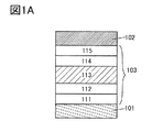
- FIG. 1A is a diagram showing the structure of a light emitting device.
- FIG. 1B is a diagram illustrating a light emitting layer.
- FIG. 2 is a conceptual diagram of energy transfer between the host material and the guest material in the light emitting layer.
- FIG. 3A is a conceptual diagram of energy transfer between a general guest material and a host material.
- FIG. 3B is a conceptual diagram of energy transfer between the guest material and the host material used for the light emitting layer.
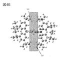
- FIG. 4A is a structural formula of the guest material used for the light emitting layer.
- FIG. 4B is a ball-and-stick model of the guest material used for the light emitting layer.
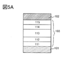
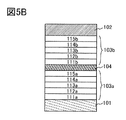
- 5A and 5B are diagrams illustrating the structure of the light emitting device.
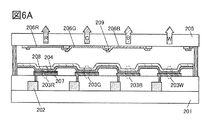
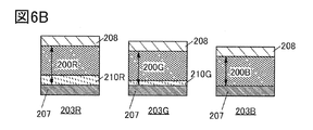
- FIG. 6A, 6B, and 6C are diagrams illustrating a light emitting device.
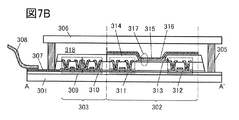
- FIG. 7A is a top view for explaining the light emitting device.
- FIG. 7B is a cross-sectional view illustrating the light emitting device.
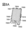
- FIG. 8A is a diagram illustrating a mobile computer.
- FIG. 8B is a diagram illustrating a portable image reproduction device.
- FIG. 8C is a diagram illustrating a digital camera.
- FIG. 8D is a diagram illustrating a mobile information terminal.
- FIG. 8E is a diagram illustrating a mobile information terminal.
- FIG. 8F is a diagram illustrating a television device.
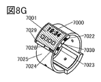
- FIG. 8G is a diagram illustrating a mobile information terminal.
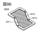
- 9A, 9B, and 9C are diagrams illustrating a foldable personal digital assistant.
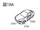
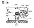
- FIG. 10A and 10B are diagrams illustrating an automobile.
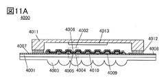
- 11A and 11B are diagrams illustrating a lighting device.
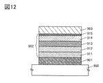
- FIG. 12 is a diagram illustrating a light emitting device.
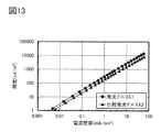
- FIG. 13 is a diagram showing the current density-luminance characteristics of the light emitting device 1 and the comparative light emitting device 2.
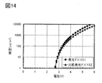
- FIG. 14 is a diagram showing voltage-luminance characteristics of the light emitting device 1 and the comparative light emitting device 2.
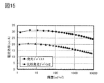
- FIG. 15 is a diagram showing the luminance-current efficiency characteristics of the light emitting device 1 and the comparative light emitting device 2.
- FIG. 16 is a diagram showing voltage-current density characteristics of the light emitting device 1 and the comparative light emitting device 2.
- FIG. 12 is a diagram illustrating a light emitting device.
- FIG. 13 is a diagram showing the current density-luminance characteristics of the light emitting device 1 and the comparative light emitting device 2.
- FIG. 14 is a diagram showing voltage-luminance characteristics of the light emitting device 1 and the comparativ
- FIG. 17 is a diagram showing the brightness-power efficiency characteristics of the light emitting device 1 and the comparative light emitting device 2.
- FIG. 18 is a diagram showing the luminance-external quantum efficiency characteristics of the light emitting device 1 and the comparative light emitting device 2.
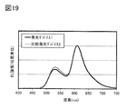
- FIG. 19 is a diagram showing electroluminescence spectra of the light emitting device 1 and the comparative light emitting device 2.
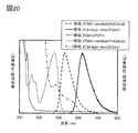
- FIG. 20 is an ultraviolet / visible absorption spectrum and an emission spectrum in a solution of 2TMS-mmtBuDPhA2Anth and [Ir (dmdppr-dmp) 2 (dpm)].
- FIG. 21 is a diagram showing the current density-luminance characteristics of the light emitting device 3, the comparative light emitting device 4, and the comparative light emitting device 5.
- FIG. 21 is a diagram showing the current density-luminance characteristics of the light emitting device 3, the comparative light emitting device 4, and the comparative light emitting device 5.
- FIG. 22 is a diagram showing voltage-luminance characteristics of the light emitting device 3, the comparative light emitting device 4, and the comparative light emitting device 5.
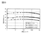
- FIG. 23 is a diagram showing the luminance-current efficiency characteristics of the light emitting device 3, the comparative light emitting device 4, and the comparative light emitting device 5.
- FIG. 24 is a diagram showing voltage-current density characteristics of the light emitting device 3, the comparative light emitting device 4, and the comparative light emitting device 5.
- FIG. 25 is a diagram showing the brightness-power efficiency characteristics of the light emitting device 3, the comparative light emitting device 4, and the comparative light emitting device 5.
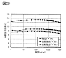
- FIG. 26 is a diagram showing the brightness-external quantum efficiency characteristics of the light emitting device 3, the comparative light emitting device 4, and the comparative light emitting device 5.
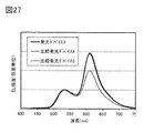
- FIG. 27 is a diagram showing electroluminescent spectra of the light emitting device 3, the comparative light emitting device 4, and the comparative light emitting device 5.
- FIG. 28 is a diagram showing the current density-luminance characteristics of the light emitting device 6 and the light emitting device 7.
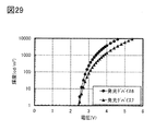
- FIG. 29 is a diagram showing voltage-luminance characteristics of the light emitting device 6 and the light emitting device 7.
- FIG. 30 is a diagram showing the luminance-current efficiency characteristics of the light emitting device 6 and the light emitting device 7.
- FIG. 31 is a diagram showing voltage-current density characteristics of the light emitting device 6 and the light emitting device 7.
- FIG. 32 is a diagram showing the brightness-power efficiency characteristics of the light emitting device 6 and the light emitting device 7.
- FIG. 33 is a diagram showing the luminance-external quantum efficiency characteristics of the light emitting device 6 and the light emitting device 7.
- FIG. 34 is a diagram showing electroluminescence spectra of the light emitting device 6 and the light emitting device 7.
- the singlet excited state (S * ) is a singlet state having excitation energy.
- the S1 level is the lowest level of the singlet excited energy level, and is the excited energy level of the lowest singlet excited state (S1 state).
- the triplet excited state (T * ) is a triplet state having excitation energy.
- the T1 level is the lowest level of the triplet excited energy level, and is the excited energy level of the lowest triplet excited state (T1 state).
- it even if it is simply described as a singlet excited state and a singlet excited energy level, it may represent an S1 state and an S1 level. Further, even when the triplet excited state and the triplet excited energy level are described, they may represent the T1 state and the T1 level.
- the fluorescent substance is a compound that emits light in the visible light region or the near infrared region when relaxing from the singlet excited state to the ground state.
- the phosphorescent substance is a compound that emits light in the visible light region or the near infrared region at room temperature when relaxing from the triplet excited state to the ground state.
- a phosphorescent substance is one of compounds capable of converting triplet excitation energy into light emission.
- the light emitting device comprises a first electrode 101 (in FIG. 1A, the case of an anode is shown) and a second electrode 102 (in FIG. 1A, a case of a cathode is shown).
- the EL layer 103 has a structure in which the EL layer 103 is sandwiched between the pair of electrodes, and the EL layer 103 has at least a light emitting layer 113, and also has a hole (hole) injection layer 111 and a hole (hole) transport layer 112. , An electron transport layer 114, an electron injection layer 115, and the like can be provided.
- the light emitting layer 113 is a layer containing a light emitting substance (guest material), and preferably has a host material in addition to the light emitting layer 113.
- the light emitting layer 113 of the light emitting device according to one aspect of the present invention has an organic compound that functions as a host material and a plurality of light emitting substances (guest materials), and specifically, as shown in FIG. 1B. It has at least a first organic compound 121 having a function of converting singlet excitation energy into light emission and a second organic compound 122 having a function of converting triplet excitation energy into light emission. It also has a third organic compound 123 that functions as a host material. Further, in the light emitting layer 113, a plurality of organic compounds that function as host materials may be used.
- the light emitted from the light emitting device is emitted from the excited state host material (including the case where a plurality of host materials form an excited complex or not) generated by the recombination of carriers (holes and electrons) in the light emitting layer 113. It is obtained by transferring energy to the guest material and causing the guest material to emit light.
- the excited state host material including the case where a plurality of host materials form an excited complex or not
- the light emitting device is a first organic compound (fluorescent light emitting substance) having a function of converting single term excitation energy into light emission from the excited state of the third organic compound 123 that functions as a host material.
- the energy transfer to the guest material (guest material) 121 and the energy transfer to the second organic compound (guest material which is a phosphorescent substance) 122 having a function of converting the triplet excitation energy into light emission occur. It has a configuration in which fluorescence emission from the first organic compound 121 and phosphorescence emission from the second organic compound 122 can be obtained. Since a TADF material can be used as the second organic compound 122 instead of the phosphorescent substance, the phosphorescent substance can be read as a TADF material, and the phosphorescent light can be read as fluorescent light emission.
- the second organic compound 122 which is a material as shown in FIG. 2, at least single-term excitation of the third organic compound 123 which functions as a host material is performed.
- the energy level (S1 level) has a higher relationship than the S1 level of the first organic compound 121 having a function of converting the single-term excitation energy into light emission, and the host material and the phosphorescent substance T1 It is necessary that energy transfer from the level to the T1 level of the fluorescent substance is unlikely to occur.
- FIG. 2 shows an example of the correlation of energy levels in the light emitting layer 113 of the light emitting device, which is one aspect of the present invention.
- the common reference numerals of FIG. 1B are used, but for convenience, the third organic compound 123 that functions as a host material is Host (123), and the singlet excitation energy has a function of converting into light emission.
- the organic compound 121 of No. 1 is referred to as a Fluorecent Guest (121), and the second organic compound 122 having a function of converting triplet excitation energy into light emission is referred to as a Phosphorecent Guest (122).
- Other notations and codes are as follows.
- ⁇ S H1 third S1 levels ⁇ T of the organic compound 123 H1: the third organic compound 123 of T1 level ⁇ S FG: S1 level ⁇ T FG of the first organic compound 121: first organic T1 level of compound 121 ⁇ S PG : T1 level of second organic compound 122 ⁇ T PG : T1 level of second organic compound 122
- the singlet excitation energy can be rapidly transferred to the first organic compound 121.
- Fig. 2 Route A 1 it is preferable that SH1 ⁇ S FG .
- S H1 ⁇ S FG drawing a tangential line at the foot of the short wavelength side of the fluorescence spectrum of the third organic compound 123, the energy of the wavelength of the extrapolation and S H1, the absorption edge of the absorption spectrum of the first organic compound 121 the energy of a wavelength upon an S FG, it is preferable that S H1 ⁇ S FG.
- the second organic compound 122 since the second organic compound 122 is a phosphorescent substance, it can receive the singlet excitation energy and the triplet excitation energy of the third organic compound 123 (FIG. 2, Route A 2 ). At this time, it is preferable that TH1 ⁇ T PG .
- the energy of the wavelength of the absorption edge of the absorption spectrum of the second organic compound 122 can be regarded as T PG.
- the wavelength energy of the emission end on the short wavelength side of the emission spectrum of the third organic compound 123 at a low temperature (for example, 10K) can be regarded as TH1 .
- SFG ⁇ TPG in order to obtain both light emission of the first organic compound 121 and the second organic compound 122 at a good ratio.
- the third organic compound 123, the first organic compound 121, and the second organic compound 122 are mixed. Therefore, between the third organic compound 123 and the first organic compound 121, triplet excitation energy of the triplet excitation energy of the third organic compound 123 in competition with the route A 1 is the first organic compound 121 the process of being converted into (FIG. 2 route A 3) can occur. Since the first organic compound 121 is a fluorescent light emitting substance, the triplet excitation energy of the first organic compound 121 does not contribute to light emission. That is, the light-emitting efficiency of the light emitting devices energy transfer route A 3 occurs is lowered.
- the energy transfer process A 3 from T H1 to T FG is not directly, once energy transfer to the triplet excited state of the higher than T FG of the first organic compound 121, T FG by subsequent internal conversion There may be a path to become, but the process is omitted in the figure.
- Undesirable thermal inactivation process in this specification since, i.e. deactivation process to T FG are all similar.
- the singlet excitation energy of the first organic compound 121 is converted into fluorescence emission and the process of energy transfer to T PG (FIG. 2). root a 4) and conflict. That is, routes A 2 and A 4 exist as pathways for the second organic compound 122 to receive excitation energy. Therefore, in order to obtain both light emission of the first organic compound 121 and the second organic compound 122 at a good ratio, the concentration of the first organic compound 121 in the light emitting layer 113 is higher than the concentration of the second organic compound 122. Higher is preferable. Further, it is preferable that the concentration of the second organic compound 122 in the light emitting layer 113 is low because the carriers are less likely to recombine in the second organic compound 122.
- the triplet excitation energy of the second organic compound 122 is converted into light emission, and the triplet excitation energy of the second organic compound 122 is converted into the triplet excitation energy of the first organic compound 121. that process (FIG. 2 route A 5) can occur in conflict. Since the first organic compound 121 is a fluorescent light emitting substance, the triplet excitation energy of the first organic compound 121 does not contribute to light emission. In other words, it decreases the luminous efficiency of the light emitting devices energy transfer route A 5 occurs.
- the emission spectrum exhibited by the second organic compound 122 preferably has an emission peak at a wavelength longer than the peak wavelength of the emission spectrum exhibited by the first organic compound 121.
- the Felster mechanism dipole-dipole interaction
- the Dexter mechanism electron exchange interaction
- the energy transfer mechanism between molecules Since the first organic compound 121, which is an energy acceptor, is a fluorescent substance, the energy transfer of Route A 3 and Route A 5 is dominated by the Dexter mechanism.
- the Dexter mechanism occurs significantly when the distance between the third organic compound 123, which is an energy donor, and the first organic compound 121, which is an energy acceptor, is 1 nm or less. Further, the Dexter mechanism is significantly generated when the distance between the first organic compound 121 and the second organic compound 122 is 1 nm or less. Therefore, in order to suppress the route A 3 and Route A 5 are, it is important to distance the distance of the energy donor and energy acceptor.
- the TFG in FIG. 2 is often an energy level derived from the luminescent group of the fluorescent luminescent substance, which is the first organic compound 121. Therefore, in order to suppress energy transfer route A 3 and Route A 5 are a third organic compound 123 and the second organic compound 122 comprising an energy donor, energy acceptor - to become the first organic compound 121 It is important to suppress the energy transfer by the Dexter mechanism by increasing the distance from the light emitting group.
- the first organic compound 121 in the mixed film of these organic compounds is used as a method for increasing the distance between the energy donor and the luminescent group of the first organic compound 121 serving as an energy acceptor.
- a method of lowering the concentration can be mentioned.
- the concentration of the first organic compound 121 in the mixed film is lowered, not only the energy transfer based on the Dexter mechanism from the energy donor to the luminescent group of the first organic compound 121 as an energy acceptor but also Felster Energy transfer based on the mechanism is also suppressed. In that case, since Route A 1 is based on the Felster mechanism, problems such as a decrease in luminous efficiency and a decrease in reliability of the light emitting device occur.
- the present inventors are energy acceptors in order to increase the distance between the first organic compound 121 which is an energy acceptor and the third organic compound 123 and the second organic compound 122 which are energy donors. It has been found that by using a fluorescent luminescent substance having a protective group as the first organic compound 121, it is possible to suppress a decrease in luminescence efficiency due to the above-mentioned energy transfer. Further, by using the first organic compound 121 having the protective group, the light emitting layer 113 having the first organic compound 121 and the second organic compound 122 emits light emitted from the first organic compound 121. It has been found that both (fluorescent emission) and emission (phosphorescent emission or fluorescent emission) derived from the second organic compound 122 can be obtained.
- FIG. 3A shows the presence of a third organic compound 123, which is a host material, and a fluorescent light emitting substance 124, which is a guest material.
- the fluorescent light emitting substance 124 is a general fluorescent light emitting substance, and is a fluorescent light emitting substance having a light emitting group 130a but not having a protecting group.
- FIG. 3B shows the presence of the third organic compound 123, which is the host material, and the first organic compound (fluorescent light emitting substance) 121, which is the guest material.
- the first organic compound 121 is a fluorescent light emitting substance used as an energy acceptor in the light emitting device according to one aspect of the present invention, and has a light emitting group 130b and a protecting group 131.
- the protecting group 131 has a function of keeping the third organic compound (host material) 123 away from the light emitting group 130b by providing a distance such that energy transfer based on the Dexter mechanism is unlikely to occur.
- the host material, the third organic compound 123, the guest material, the fluorescent light emitting substance 124, or the first organic compound (fluorescent light emitting substance) 121 is any Also exists in a close position. Therefore, as shown in FIG. 3A, when the fluorescent light emitting substance 124 does not have a protective group, the distance between the light emitting group 130a and the third organic compound 123 becomes short, so that the third organic compound 123 emits fluorescence. As energy transfer to the substance 124, both energy transfer by the Felster mechanism (Route A 6 in FIG. 3A) and energy transfer by the Dexter mechanism (Route A 7 in FIG. 3A) can occur.
- the triplet excitation energy is transferred from the host material to the guest material by the Dexter mechanism, and the guest material is a fluorescent luminescent material even if the triplet excited state of the guest material is generated, there is no triplet excitation energy. Since the radiation is deactivated, it contributes to a decrease in the light emission efficiency of the light emitting device.
- the luminescent group (130a, 130b) refers to an atomic group (skeleton) that causes light emission in a fluorescent luminescent substance.
- the luminescent group (130a, 130b) generally has a ⁇ bond, preferably contains an aromatic ring, and preferably has a condensed aromatic ring or a condensed heteroaromatic ring.
- the atomic group (skeleton) including the aromatic ring in which the transition dipole vector exists on the ring plane can be regarded as the light emitting group (130a, 130b).
- the fluorescent substance has a skeleton having the lowest S1 level among the plurality of condensed aromatic rings or condensed heteroaromatic rings. It may be regarded as a luminous group of.
- the skeleton having the absorption end on the longest wavelength side may be regarded as the luminescent group of the fluorescent light emitting substance.
- condensed aromatic ring or condensed heteroaromatic ring examples include a phenanthrene skeleton, a stilbene skeleton, an acridone skeleton, a phenoxazine skeleton, and a phenothiazine skeleton.
- a fluorescent substance having a naphthalene skeleton, anthracene skeleton, fluorene skeleton, chrysene skeleton, triphenylene skeleton, tetracene skeleton, pyrene skeleton, perylene skeleton, coumarin skeleton, quinacridone skeleton, and naphthobisbenzofuran skeleton is preferable because of its high fluorescence quantum yield. ..
- the protecting group 131 of the first organic compound (fluorescent light emitting substance) 121 shown in FIG. 3B is a T1 level higher than the T1 level of the light emitting group 130b and the third organic compound 123 which is the host material. It is preferable to have a position. Therefore, a saturated hydrocarbon group can be preferably used as a protecting group. Saturated hydrocarbon groups have a high T1 level because they do not have ⁇ bonds, and have a low function of transporting carriers (electrons or holes). Therefore, since the first organic compound 121 has a saturated hydrocarbon group as the protective group 131, the light emitting group has almost no effect on the excited state and carrier transportability of the third organic compound 123, which is the host material. The distance between 130b and the third organic compound 123, which is the host material, can be increased.
- the frontier orbital ⁇ HOMO is on the substituent side having the ⁇ -conjugated system.
- LUMO Large Unoccupied Molecular Orbital, also referred to as the lowest empty orbital
- the luminous group 130b often has a frontier orbital.
- the overlap of HOMOs of both the energy donor and the energy acceptor and the overlap of both LUMOs are important.
- the protecting group 131 include alkyl groups having 1 or more and 10 or less carbon atoms. Further, the protecting group 131 may have a bulky structure because it is necessary to keep the distance between the light emitting group 130b of the first organic compound 121 which is the guest material and the third organic compound 123 which is the host material. preferable. Therefore, an alkyl group having 3 to 10 carbon atoms, a substituted or unsubstituted cycloalkyl group having 3 to 10 carbon atoms, and a trialkylsilyl group having 3 to 10 carbon atoms can be preferably used. In particular, as the alkyl group, a bulky branched chain alkyl group is preferable. Further, it is particularly preferable that the substituent has a quaternary carbon because it becomes a bulky substituent.
- the protecting group 131 does not directly bond with the light emitting group 130b.
- the protecting group 131 and the luminescent group 130b are bonded to each other via a divalent or higher valent substituent such as an arylene group or an amino group. By binding the protecting group 131 and the luminescent group 130b via the substituent, the distance between the luminescent group 130b and the third organic compound 123 can be effectively increased.
- the protecting group 131 and the luminescent group 130b are bound to each other via the substituent, it is preferable to have four or more protecting groups for one luminescent group because the Dexter mechanism can be effectively suppressed. ..
- the divalent or higher valent substituent connecting the light emitting group 130b and the protecting group 131 is preferably a substituent having a ⁇ -conjugated system.
- the physical properties such as the emission color, HOMO level, and glass transition point of the first organic compound 121, which is a guest material, can be adjusted.
- the protecting group 131 is arranged on the outermost side when the molecular structure is viewed centering on the luminescent group.
- the energy transfer of the first organic compound 121 is suppressed by the Dexter mechanism, energy is received from the third organic compound 123 by the Felster mechanism in order for the first organic compound 121 to emit light.
- the energy transfer by the Felster mechanism is also affected by the distance between the host material and the guest material.
- the Dexter mechanism is dominant when the distance between the host material and the guest material is 1 nm or less
- the Felster mechanism is dominant when the distance is 1 nm or more and 10 nm or less.
- it is said that energy transfer is unlikely to occur when the distance between the host material and the guest material is 10 nm or more.
- the distance between the third organic compound 123, which is the above-mentioned host material, and the first organic compound 121, which is the guest material, is the distance between the third organic compound 123 and the first organic compound. It is assumed that it is equal to the distance of the light emitting group 130b of 121. Therefore, it is preferable that the protecting group 131 contained in the first organic compound 121 spreads from the luminescent group 130b contained in the first organic compound 121 to a range of 1 nm or more and 10 nm or less, so that the Felster mechanism can be predominant. ..
- the spread of the protecting group 131 of the first organic compound 121 is more preferably in the range of 1 nm or more and 5 nm or less.
- the concentration ratio of the fluorescent light-emitting substance as the guest material it is preferable to increase the concentration ratio of the fluorescent light-emitting substance as the guest material to the host material, but if the concentration ratio of the guest material is increased, Dexter There is a trade-off relationship that the transfer speed of energy transfer by the mechanism is improved, and as a result, the light emission efficiency is decreased. Therefore, increasing the concentration ratio of the guest material has not been an effective means for improving the luminous efficiency.
- the first organic compound 121 used in the light emitting device has a structure capable of suppressing energy transfer by the Dexter mechanism from the host material, and therefore is used as a guest material in the light emitting layer.
- the energy transfer efficiency by the Felster mechanism can be increased (energy transfer speed is improved) by increasing the concentration ratio with respect to the host material.
- the excitation lifetime of the guest material (energy acceptor) in the light emitting layer can be shortened, so that the reliability of the light emitting device can be shortened. Can be improved.
- the concentration of the first organic compound 121 as a guest material is 2 wt% or more and 30 wt% or less with respect to the third organic compound 123 as a host material. Is preferable, and more preferably 5 wt% or more and 20 wt% or less, and further preferably 5 wt% or more and 15 wt% or less. With this configuration, the energy transfer speed by the Felster mechanism can be increased, so that a light emitting device having high luminous efficiency can be obtained.
- the light emitting layer of the light emitting device has a second organic compound 122 having a function of converting triplet excitation energy into light emission as a guest material. Therefore, the light emitting device according to one aspect of the present invention emits high amounts of both fluorescent light emitted from the first organic compound 121 and light emitted from the second organic compound 122 (phosphorescent light emission or fluorescent light emission). It can be obtained with efficiency.
- the concentration of the first organic compound 121 in the light emitting layer 113 is higher than the concentration of the second organic compound 122. Is also preferable.
- the above-mentioned energy transfer always competes with the quenching process due to the influence of deteriorated substances and impurities. That is, when the quenching rate constant in the quenching process increases with time, the ratio of light emission in the light emitting device decreases, and the brightness of the light emitting device deteriorates.
- the light emitting device according to one aspect of the present invention can increase the energy transfer rate by the Felster mechanism while suppressing the energy transfer by the Dexter mechanism, so that it competes with the quenching process. It is possible to reduce the influence of the light emitting device and extend the life of the light emitting device.
- ⁇ Felster mechanism In the Felster mechanism, energy transfer does not require direct contact between molecules, and energy transfer occurs through the resonance phenomenon of dipole oscillations of the third organic compound and the first organic compound. Due to the resonance phenomenon of dipole vibration, the third organic compound transfers energy to the first organic compound, the third organic compound in the excited state becomes the ground state, and the first organic compound in the ground state becomes the excited state. ..
- the rate constant kh * ⁇ g of the Felster mechanism is shown in the mathematical formula (1).
- Equation (1) [nu denotes a frequency, f 'h ( ⁇ ), when discussing the energy transfer from the third normalized emission spectrum (singlet excited state of the organic compound fluorescence spectrum, When discussing the energy transfer from the triple-term excited state, it represents the phosphorescence spectrum), ⁇ g ( ⁇ ) represents the molar absorption coefficient spectrum of the first organic compound, N represents the avocadro number, and n represents the medium.
- R represents the intermolecular distance between the third organic compound and the first organic compound, ⁇ represents the measured lifetime of the excited state (fluorescence lifetime or phosphorescent lifetime), and c is.
- the emission colors of the third organic compound and the first organic compound are close to each other, according to the above formula (1).
- f 'h ( ⁇ ) and epsilon g ([nu) overlap is small ( ⁇ g ( ⁇ ) is present in the longer wavelength side than the emission spectrum of the first organic compound) for, k from equation (1) h * ⁇ g becomes smaller.
- the concentration of the energy donor in the light emitting layer can be increased as described above, the value of R in the formula (1) can be increased, and kh *. ⁇ The decrease in g can be suppressed.
- a fluorescent light emitting substance having a light emitting color close to that of the energy donor can be used as the light emitting material.
- the light emitting device of one aspect of the present invention can be used even if the light emitting colors of the energy donor and the energy acceptor are different.
- h Planck's constant and K is a constant having an energy dimension.
- ⁇ represents a frequency.
- f 'h ( ⁇ ) when when discussing the energy transfer from the third normalized emission spectrum (singlet excited state of the organic compound discussed fluorescence spectrum, the energy transfer from a triplet excited state Phosphorescent spectrum).
- ⁇ 'g ( ⁇ ) denotes a normalized absorption spectrum of the first organic compound.
- L represents an effective molecular radius.
- R represents the intermolecular distance between the third organic compound and the first organic compound.
- the energy transfer efficiency ⁇ ET from the third organic compound to the first organic compound is expressed by the mathematical formula (3).
- k r the emission process of the third organic compound (In discussing the energy transfer from a singlet excited state fluorescence and phosphorescence if the energy transfer from a triplet excited state) represents the rate constant
- k n is , Represents the rate constant of the non-luminescence process (heat deactivation and intersystem crossing) of the first organic compound.
- ⁇ represents the lifetime of the excited state of the third organic compound actually measured.
- the energy transfer efficiency ⁇ ET shows that the excited state of the third organic compound does not depend on the lifetime ⁇ . Further, it can be said that the energy transfer efficiency ⁇ ET should have a high emission quantum yield ⁇ .
- the emission spectrum of the third organic compound and the absorption spectrum of the first organic compound have a large overlap.
- the first organic compound has a high molar extinction coefficient. This means that the emission spectrum of the third organic compound and the absorption band appearing on the longest wavelength side of the first organic compound overlap. Since the direct transition from the singlet ground state to the triplet excited state in the first organic compound is prohibited, the molar extinction coefficient related to the triplet excited state in the first organic compound is a negligible amount.
- the energy transfer rate by the Felster mechanism is inversely proportional to the sixth power of the intermolecular distance R between the third organic compound and the first organic compound according to the mathematical formula (1).
- R is 1 nm or less
- energy transfer by the Dexter mechanism becomes predominant. Therefore, in order to increase the energy transfer rate by the Dexter mechanism while suppressing the energy transfer by the Dexter mechanism, the intermolecular distance must be increased. It is preferably 1 nm or more and 10 nm or less. Therefore, since the above-mentioned protecting group is required not to be too bulky, the number of carbon atoms constituting the protecting group is preferably 3 or more and 10 or less.
- the emission spectrum of the third organic compound fluorescence spectrum when discussing energy transfer from the single-term excited state, triple-term excited state.
- the larger the overlap between the phosphorescence spectrum) and the absorption spectrum of the first organic compound is better. .. Therefore, the optimization of the energy transfer efficiency is realized by overlapping the emission spectrum of the third organic compound and the absorption band appearing on the longest wavelength side of the first organic compound.
- the energy transfer efficiency ⁇ ET in the Dexter mechanism depends on ⁇ . Since the Dexter mechanism is an energy transfer process based on electron exchange, the energy transfer of the third organic compound from the singlet excited state of the third organic compound to the singlet excited state of the first organic compound is similar to that of the third organic compound. Energy transfer from the triplet excited state to the triplet excited state of the first organic compound also occurs.
- the first organic compound is a fluorescent light emitting substance
- the energy transfer efficiency of the first organic compound to the triplet excited state is low. That is, the energy transfer efficiency based on the Dexter mechanism from the third organic compound to the first organic compound is preferably low, and the energy transfer efficiency based on the Felster mechanism from the third organic compound to the first organic compound is high. High is preferable.
- the energy transfer efficiency in the Felster mechanism does not depend on the lifetime ⁇ in the excited state of the third organic compound.
- the energy transfer efficiency in the Dexter mechanism depends on the excitation lifetime ⁇ of the third organic compound. Therefore, in order to reduce the energy transfer efficiency in the Dexter mechanism, the excitation lifetime ⁇ of the third organic compound is short. preferable.
- a fluorescent light emitting substance having a protecting group is used as the first organic compound. Therefore, the intermolecular distance between the third organic compound and the first organic compound can be increased, and the energy transfer by the Dexter mechanism can be suppressed. Therefore, the triple-term excitation energy of the third organic compound is the third by the Dexter mechanism. It is possible to move to the organic compound of 1 and suppress non-radiation deactivation. This makes it possible to provide a light emitting device having high luminous efficiency.
- the light emitting layer of the light emitting device has a host material and a guest material, and the guest material is a material (fluorescent light emitting material) having a function of converting single-term excitation energy into light emission.
- the organic compound 121 of 1 and the second organic compound 122 which is a material (phosphorescent substance or TADF material) having a function of converting triple-term excitation energy into light emission are used.
- the first organic compound 121 will be described in detail.
- the first organic compound 121 which is a material (fluorescent light emitting substance) having a function of converting singlet excitation energy into light emission, has a light emitting group 130b and a protecting group 131.
- a condensed aromatic ring or a condensed heteroaromatic ring can be used as the light emitting group 130b.
- the protective group 131 contained in the first organic compound 121 includes an alkyl group having 1 to 10 carbon atoms, a cycloalkyl group having 3 to 10 carbon atoms, a branched alkyl group having 3 to 10 carbon atoms, and carbon.
- a trialkylsilyl group having a number of 3 or more and 12 or less is preferable. Since the first organic compound 121 has the protecting group 131, it is possible to suppress the energy transfer by the Dexter mechanism from the host material to the guest material, the first organic compound 121, in the light emitting layer.
- the first organic compound 121 has a light emitting group 130b and two or more diarylamino groups having an aryl group bonded to each other, and each of the aryl groups has at least two protecting groups 131.
- the quantum yield of the first organic compound 121 can be increased by binding two or more diarylamino groups at positions symmetrical with respect to the luminescent group 130b.
- a diphenylamino group is preferable. By using the diphenylamino group, the increase in the molecular weight of the first organic compound 121 can be suppressed and the sublimation property can be maintained.
- the protecting group 131 can be arranged so as to cover the luminescent group 130b, so that the protecting group 131 can be arranged from any direction. It is preferable because the distance between the host material and the light emitting group 130b can be increased.
- the first organic compound 121 preferably has a structure in which one light emitting group 130b has four or more protecting groups 131.
- a diphenylamino group is used as a specific example of the diarylamino group contained in the first organic compound 121, it is preferable to have a protecting group 131 at the 3rd and 5th positions of the phenyl group in the diphenylamino group.
- the light emitting group 130b contained in the first organic compound 121 is covered with the protecting group 131 from above and below in the plane direction thereof, the energy transfer from the host material to the light emitting group 130b by the Dexter mechanism is suppressed. Can be done.
- One aspect of the first organic compound 121 shown above is represented by the following general formula (G1).
- A represents a substituted or unsubstituted fused aromatic ring having 10 to 30 carbon atoms or a substituted or unsubstituted fused heteroaromatic ring having 10 to 30 carbon atoms
- Ar 1 to Ar 4 are respectively.
- it represents an aromatic hydrocarbon group having 6 to 13 carbon atoms substituted or unsubstituted
- X 1 to X 8 independently represent an alkyl group having 1 to 10 carbon atoms, and 3 substituted or unsubstituted carbon atoms. It represents any one of a cycloalkyl group having 10 or more carbon atoms and a trialkylsilyl group having 3 to 10 carbon atoms.
- Ar 5 or Ar 6 each independently represents a substituted or unsubstituted aromatic hydrocarbon group having 6 to 13 carbon atoms, and X 9 to X 12 independently represent 1 carbon atoms. It represents any one of an alkyl group of 10 or more, a substituted or unsubstituted cycloalkyl group having 3 or more and 10 or less carbon atoms, and a trialkylsilyl group having 3 or more and 10 or less carbon atoms, and R 1 to R 10 are independent of each other.
- Hydrogen an alkyl group having 3 or more and 10 or less carbon atoms, a substituted or unsubstituted cycloalkyl group having 3 or more and 10 or less carbon atoms, and a trialkylsilyl group having 3 or more and 12 or less carbon atoms.
- the protecting group 131 represented by X 9 to X 12 emits light via the aromatic hydrocarbon group represented by Ar 5 or Ar 6. It has a structure linked to the quinacridone skeleton of group 130b. With this structure, the protecting group 131 can be arranged so as to cover the light emitting group 130b, so that energy transfer by the Dexter mechanism can be suppressed. In addition, it may have a protecting group 131 that directly binds to the light emitting group 130b.
- Another aspect of the first organic compound 121 shown above is represented by the following general formula (G3).
- A represents a substituted or unsubstituted fused aromatic ring having 10 to 30 carbon atoms or a substituted or unsubstituted condensed complex aromatic ring having 10 to 30 carbon atoms
- X 1 to X 8 are respectively. It independently represents any one of an alkyl group having 1 to 10 carbon atoms, a substituted or unsubstituted cycloalkyl group having 3 to 10 carbon atoms, and a trialkylsilyl group having 3 to 10 carbon atoms.
- the protective group 131 represented by X 1 to X 8 is, via a phenylene group, coupled with luminophores 130b represented by A structure Has. Further, it is preferable that the two protecting groups 131 bonded to one phenylene group are bonded at the meta position of the phenylene group. With this structure, the protecting group 131 can be arranged so as to cover the light emitting group 130b, so that energy transfer by the Dexter mechanism can be suppressed. In addition, it may have a protecting group 131 that directly binds to the light emitting group 130b.
- X 9 to X 12 are independently alkyl groups having 1 to 10 carbon atoms, substituted or unsubstituted cycloalkyl groups having 3 to 10 carbon atoms, and 3 to 10 carbon atoms.
- R 1 , R 3 , R 6 and R 8 are independently hydrogen, an alkyl group having 3 or more and 10 or less carbon atoms, a substituted or unsubstituted cycloalkyl group having 3 or more and 10 or less carbon atoms, and 3 or more and 12 or less carbon atoms.
- the first organic compound 121 represented by the general formula (G4) has a structure in which the protecting group 131 represented by X 9 to X 12 is bonded to the quinacridone skeleton which is the luminescent group 130b via a phenylene group. Have. Further, it is preferable that the two protecting groups 131 bonded to one phenylene group are bonded at the meta position of the phenylene group. With this structure, the protecting group 131 can be arranged so as to cover the light emitting group 130b, so that energy transfer by the Dexter mechanism can be suppressed. In addition, it may have a protecting group 131 that directly binds to the light emitting group 130b.
- X 1 to X 8 are independently alkyl groups having 1 or more and 10 or less carbon atoms, substituted or unsubstituted cycloalkyl groups having 3 or more and 10 or less carbon atoms, and 3 or more and 10 or less carbon atoms. of represent any one of a trialkylsilyl group, each R 11 to R 18 are independently hydrogen, a branched alkyl group having 3 to 10 carbon atoms, a substituted or unsubstituted C 3 to 10 cycloalkyl It represents any one of a group, a trialkylsilyl group having 3 to 10 carbon atoms, and an substituted or unsubstituted aryl group having 6 to 25 carbon atoms.
- the luminescent group 130b contained in the first organic compound 121 represented by the general formula (G1) and the general formula (G3) has a substituted or unsubstituted condensed aromatic ring having 10 to 30 carbon atoms or 10 to 10 carbon atoms. It is represented by a substituted or unsubstituted fused complex aromatic ring of 30. Further, the luminescent group 130b contained in the first organic compound 121 represented by the general formula (G2), the general formula (G4) and the general formula (G5) is a quinacridone skeleton represented in the formula.
- X 1 to X 12 in the general formula (G1), the general formula (G2), the general formula (G3), the general formula (G4) and the general formula (G5) are the first organic compounds 121 thereof. Represents the protecting group 131 possessed by.
- examples of the substituted or unsubstituted fused aromatic ring having 10 to 30 carbon atoms or the substituted or unsubstituted condensed complex aromatic ring having 10 to 30 carbon atoms include, for example. Examples thereof include a phenanthrene skeleton, a stillben skeleton, an acridone skeleton, a phenoxazine skeleton, and a phenothiazine skeleton.
- naphthalene skeleton, anthracene skeleton, fluorene skeleton, chrysene skeleton, triphenylene skeleton, tetracene skeleton, pyrene skeleton, perylene skeleton, coumarin skeleton, quinacridone skeleton, naphthobisbenzofuran skeleton, etc. which can further increase the fluorescence quantum yield, are mentioned. Be done.
- the aromatic hydrocarbon group having 6 to 13 carbon atoms includes a phenyl group, a biphenyl group, and a naphthyl. Groups, fluorenyl groups and the like can be mentioned.
- alkyl group having 1 or more and 10 or less carbon atoms include, for example, a methyl group. Examples thereof include an ethyl group, a propyl group, a pentyl group and a hexyl group.
- cycloalkyl groups having 3 or more and 10 or less carbon atoms are used.
- a cyclopropyl group, a cyclobutyl group, a cyclohexyl group, a norbornyl group, an adamantyl group and the like can be mentioned.
- Alkyl group having 1 to 7 carbon atoms such as a group, cyclopentyl group, cyclohexyl group, cycloheptyl group, cycloalkyl group having 5 to 7 carbon atoms such as 8,9,10-trinorbornanyl group, phenyl Examples thereof include an aryl group having 6 to 12 carbon atoms such as a group, a naphthyl group and a biphenyl group.
- specific examples of the branched alkyl group having 3 or more and 10 or less carbon atoms include, for example, an isopropyl group, a sec-butyl group, an isobutyl group, a tert-butyl group, an isopentyl group, and a sec-pentyl group.
- examples thereof include a group, a tert-pentyl group, a neopentyl group, an isohexyl group, a 3-methylpentyl group, a 2-methylpentyl group, a 2-ethylbutyl group, a 1,2-dimethylbutyl group and a 2,3-dimethylbutyl group.
- trialkylsilyl group having 3 or more and 12 or less carbon atoms in the above general formula (G1), general formula (G2), general formula (G3), general formula (G4), and general formula (G5) for example, a trimethylsilyl group, a triethylsilyl group, a tert-butyldimethylsilyl group and the like can be mentioned.
- a condensed aromatic ring In the above general formula (G1), general formula (G2), general formula (G3), and general formula (G4), a condensed aromatic ring, a condensed heteroaromatic ring, an aromatic hydrocarbon group having 6 to 13 carbon atoms, or carbon.
- the substituents include a methyl group, an ethyl group, a propyl group, an isopropyl group, a butyl group, an isobutyl group, a sec-butyl group, a tert-butyl group and a pentyl.
- An alkyl group having 1 to 7 carbon atoms such as a group or a hexyl group, or a cycloalkyl group having 5 to 7 carbon atoms such as a cyclopentyl group, a cyclohexyl group, a cycloheptyl group, or an 8,9,10-trinorbornanyl group.
- Examples thereof include an aryl group having 6 to 12 carbon atoms such as a group, a phenyl group, a naphthyl group and a biphenyl group.
- aryl group having 6 or more and 25 or less carbon atoms in the above general formula (G5) include a phenyl group, a naphthyl group, a biphenyl group, a fluorenyl group, a spirofluorenyl group and the like.
- the aryl group has a substituent, the above-mentioned alkyl group having 1 to 10 carbon atoms, a branched alkyl group having 3 to 10 carbon atoms, and a substituted or unsubstituted cycloalkyl having 3 to 10 carbon atoms. Examples thereof include a trialkylsilyl group having 3 or more and 10 or less carbon atoms.
- the first organic compound 121 represented by the general formula (G5) has a structure in which the protecting group 131 represented by X 1 to X 8 is bonded to the anthracene skeleton which is the luminescent group 130b via a phenylene group. Have. Further, it is preferable that the two protecting groups 131 bonded to one phenylene group are bonded at the meta position of the phenylene group. In this structure, since the anthracene skeleton has a small light emitting surface area, the protecting group 131 can efficiently cover the light emitting group 130b, and the energy transfer by the Dexter mechanism can be suppressed.
- first organic compound 121 represented by the general formulas (G1) to (G5) are described in the following structural formulas (100) to structural formulas (105) and structural formulas (200) to structures. It is shown in the formula (284). Specific examples of the first organic compound 121 represented by the general formulas (G1) to (G5) are not limited thereto.
- the structure of the first organic compound 121 will be described using ⁇ bis (3,5-di-tert-butylphenyl) amine (abbreviation: 2tBu-mmtBuDPhA2Anth).
- the luminescent group 130b in 2tBu-mmtBuDPhA2Anth is an anthracene ring
- the protecting group 131 is a tertiary butyl group (tBu).
- FIG. 4A shows 2tBu-mmtBuDPhA2Anth
- FIG. 4B shows a ball-and-stick model when 2tBu-mmtBuDPhA2Anth is viewed from the direction of the arrow in FIG. 4A (horizontal direction with respect to the surface of the anthracene ring).
- the shaded portion of FIG. 4B represents the portion directly above the surface of the anthracene ring, which is the light emitting group 130b, and has a region where the tBu group, which is a protecting group, overlaps the portion directly above the shaded portion.
- the atom indicated by the arrow (a) is a carbon atom of a tBu group that overlaps the shaded portion
- the atom indicated by the arrow (b) is a hydrogen atom of a tBu group that overlaps the shaded portion. is there.
- the atom constituting the protecting group 131 is located directly above one surface of the light emitting group 130b, and the atom constituting the protecting group 131 is also located directly above the other surface of the light emitting group 130b.
- the first organic compound 121 which is a guest material
- the third organic compound 123 which is a host material
- the plane direction and the vertical direction of the anthracene ring which is the light emitting group 130b The distance between both directions and the host material can be increased, and energy transfer by the Dexter mechanism can be suppressed.
- the Dexter mechanism For energy transfer by the Dexter mechanism, for example, when the transition related to energy transfer is a transition between HOMO and LUMO, the Dexter mechanism occurs significantly when the HOMO and LUMO of both the host material and the guest material overlap. Therefore, the Dexter mechanism can be suppressed by suppressing the overlap of HOMO and LUMO of both materials. That is, the Dexter mechanism can be suppressed by increasing the distance between the skeleton involved in the excited state and the guest material.
- the luminescent group 130b in the second organic compound 121 which is a fluorescent luminescent substance, the luminescent group 130b often has HOMO and LUMO. Therefore, in 2tBu-mmtBuDPhA2Anth shown in FIG. 4B, it is important that HOMO and LUMO spreading above and below the anthracene ring of the luminescent group 130b have a molecular structure covered with the protecting group 131 in order to suppress the Dexter mechanism. Is.
- 2tBu-mmtBuDPhA2Anth has a region where the tBu group, which is the protecting group 131, overlaps directly above the surface where the transition dipole vector exists, that is, the surface of the anthracene ring, which is the light emitting group 130b. Then it is preferable. Specifically, at least one of the atoms constituting the plurality of protective groups 131 (tBu group in FIG.
- A represents a substituted or unsubstituted fused aromatic ring having 10 to 30 carbon atoms or a substituted or unsubstituted fused heteroaromatic ring having 10 to 30 carbon atoms
- Ar 1 to Ar 4 are respectively.
- it represents an aromatic hydrocarbon group having 6 to 13 carbon atoms substituted or unsubstituted
- X 1 to X 8 independently represent an alkyl group having 1 to 10 carbon atoms, and 3 substituted or unsubstituted carbon atoms. It represents any one of a cycloalkyl group having 10 or more carbon atoms and a trialkylsilyl group having 3 to 10 carbon atoms.
- the first organic compound 121 represented by the general formula (G1) can be synthesized, for example, by the methods shown in the following synthesis scheme (S-1) and synthesis scheme (S-2).
- compound 4 (diamine compound) is obtained by coupling compound 1, compound 2 (arylamine), and compound 3 (arylamine).
- A is a substituted or unsubstituted fused aromatic ring having 10 to 30 carbon atoms or a substituted or unsubstituted fused heteroaromatic ring having 10 to 30 carbon atoms.
- Ar 1 to Ar 4 represent aromatic hydrocarbon groups having 6 to 13 carbon atoms independently substituted or unsubstituted
- X 1 to X 8 independently represent alkyl groups having 1 to 10 carbon atoms. Represents any one of a substituted or unsubstituted cycloalkyl group having 3 or more and 10 or less carbon atoms and a trialkylsilyl group having 3 or more and 12 or less carbon atoms.
- condensed ring or condensed heteroaromatic ring examples include chrysene, phenanthrene, stilbene, acridone, phenoxazine, phenothiazine and the like.
- anthracene, pyrene, coumarin, quinacridone, perylene, tetracene, and naphthobisbenzofuran are preferable.
- X 10 to X 13 represent a halogen group or a triflate group, and the halogen is a halogen. Iodine or bromine or chlorine is preferred.
- palladium compounds such as bis (dibenzilidenacetone) palladium (0) and palladium (II) acetate, tri (tert-butyl) phosphine, tri (n-hexyl) phosphine, tricyclohexylphosphine, and di (1-) Ligsins such as adamantyl) -n-butylphosphine, 2-dicyclohexylphosphino-2', 6'-dimethoxy-1,1'-biphenyl can be used.
- an organic base such as sodium tert-butoxide and an inorganic base such as potassium carbonate, cesium carbonate and sodium carbonate can be used.
- toluene, xylene, mesitylene, benzene, tetrahydrofuran, dioxane and the like can be used as the solvent, toluene, xylene, mesitylene, benzene, tetrahydrofuran, dioxane and the like.
- the reagents that can be used in the reaction are not limited to these reagents.
- the reactions carried out in the above synthetic schemes (S-1) and (S-2) are not limited to the Buchwald-Hartwig reaction, but are the Ullmann-Kosugi-Still coupling reaction and Grignard reagent using an organotin compound. Coupling reaction using, copper, Ullmann reaction using a copper compound, or the like can be used.
- the compound 1 and the compound 2 are reacted first to form a coupling body, and the obtained coupling body and the compound are obtained. It is preferable to react with 3.
- compound 1 is preferably a dihalogen, and X 10 and X 11 are selectively one using different halogens. It is preferable to carry out the amination reaction one by one.
- FIG. 5A shows an example of a light emitting device having an EL layer including a light emitting layer between a pair of electrodes. Specifically, it has a structure in which the EL layer 103 is sandwiched between the first electrode 101 and the second electrode 102.
- the hole (ball) injection layer 111, the hole (hole) transport layer 112, the light emitting layer 113, the electron transport layer 114, and the electron injection layer 115 has a structure in which the functional layers are sequentially laminated.
- the light emitting layer 113 has a host material and a guest material, uses a third organic compound 123 as the host material, and has a function of converting singlet excitation energy into light emission as the guest material (fluorescence emission).
- a first organic compound 121 which is a substance) and a second organic compound 122 which is a material (phosphorescent substance or TADF material) having a function of converting triplet excitation energy into light emission are used.
- a light emitting device capable of low voltage drive by having a configuration (tandem structure) having a plurality of EL layers formed by sandwiching a charge generation layer between a pair of electrodes, and a light emitting device.
- a light emitting device or the like whose optical characteristics are improved by forming a micro optical resonator (microcavity) structure between a pair of electrodes is also included in one aspect of the present invention.
- the charge generation layer has a function of injecting electrons into one adjacent EL layer and injecting holes into the other EL layer when a voltage is applied to the first electrode 101 and the second electrode 102. Have.
- At least one of the first electrode 101 and the second electrode 102 of the light emitting device is a translucent electrode (transparent electrode, semi-transmissive / semi-reflective electrode, etc.).
- the electrode having translucency is a transparent electrode
- the transmittance of visible light of the transparent electrode is 40% or more.
- the reflectance of visible light of the semi-transmissive / semi-reflective electrode is 20% or more and 80% or less, preferably 40% or more and 70% or less.
- these electrodes preferably have a resistivity of 1 ⁇ 10 -2 ⁇ cm or less.
- the reflective electrode when one of the first electrode 101 and the second electrode 102 is a reflective electrode (reflecting electrode), the reflective electrode is visible.
- the reflectance of light is 40% or more and 100% or less, preferably 70% or more and 100% or less.
- this electrode preferably has a resistivity of 1 ⁇ 10 -2 ⁇ cm or less.
- the following materials can be appropriately combined and used as long as the functions of both electrodes described above can be satisfied.
- metals, alloys, electrically conductive compounds, and mixtures thereof can be appropriately used. Specific examples thereof include In—Sn oxide (also referred to as ITO), In—Si—Sn oxide (also referred to as ITSO), In—Zn oxide, and In—W—Zn oxide.
- Ni Indium (In), Tin (Sn), Molybdenum (Mo), Tantal (Ta), Tungsten (W), Palladium (Pd), Gold (Au), Platinum (Pt), Silver (Ag), Ittrium (Y) ), Neodymium (Nd) and other metals, and alloys containing these in appropriate combinations can also be used.
- Other elements belonging to Group 1 or Group 2 of the Periodic Table of Elements eg, Lithium (Li), Cesium (Cs), Calcium (Ca), Strontium (Sr)), Europium (Eu), Ytterbium Rare earth metals such as (Yb), alloys containing these in appropriate combinations, and other graphenes can be used.
- a sputtering method or a vacuum vapor deposition method can be used for producing these electrodes.
- the hole injection layer 111 is a layer for injecting holes into the EL layer 103 from the first electrode 101, which is an anode, and is a layer containing an organic acceptor material and a material having a high hole injection property.
- the organic acceptor material is a material capable of generating holes in the organic compound by separating charges between the LUMO level value and another organic compound having a HOMO level close to each other. is there. Therefore, as the organic acceptor material, a compound having an electron-withdrawing group (halogen group or cyano group) such as a quinodimethane derivative, a chloranyl derivative, or a hexaazatriphenylene derivative can be used.
- halogen group or cyano group such as a quinodimethane derivative, a chloranyl derivative, or a hexaazatriphenylene derivative
- HAT-CN 3,6- difluoro -2,5,7,7,8, 8-Hexacyanoquinodimethane
- Chloranil 2,3,6,7,10,11-Hexacyano-1,4,5,8,9,12-Hexaazatriphenylene
- F6-TCNNQ 1,3 4,5,7,8-hexafluorotetracyano-naphthoquinodimethane
- HAT-CN 3,6- difluoro -2,5,7,7,8, 8-Hexacyanoquinodimethane
- Chloranil 2,3,6,7,10,11-Hexacyano-1,4,5,8,9,12-Hexaazatriphenylene
- F6-TCNNQ 1,3 4,5,7,8-hexafluorotetracyano-naphthoquinodimethane
- F6-TCNNQ 1,3 4,5,7,8-hexafluorotetracyano-naphthoquinodimethane
- the [3] radialene derivative is preferable because it has very high electron acceptability, and specifically, ⁇ , ⁇ ', ⁇ ''-1,2,3-cyclopropanetriylidentris [4-cyano-].
- 2,3,5,6-tetrafluorobenzene acetonitrile] ⁇ , ⁇ ', ⁇ ''-1,2,3-cyclopropanetriylidentris [2,6-dichloro-3,5-difluoro-4- (2,6-dichloro-3,5-difluoro-4- (" Trifluoromethyl) benzene acetonitrile]
- ⁇ , ⁇ ', ⁇ ''-1,2,3-cyclopropanetriylidentris [2,3,4,5,6-pentafluorobenzene acetonitrile] and the like can be used. ..
- Examples of the material having high hole injection properties include transition metal oxides such as molybdenum oxide, vanadium oxide, ruthenium oxide, tungsten oxide, and manganese oxide.
- transition metal oxides such as molybdenum oxide, vanadium oxide, ruthenium oxide, tungsten oxide, and manganese oxide.
- low molecular weight compounds such as 4,4', 4''-tris (N, N-diphenylamino) triphenylamine (abbreviation: TDATA), 4,4', 4''-tris [N- (3-Methylphenyl) -N-phenylamino] triphenylamine (abbreviation: MTDATA), 4,4'-bis [N- (4-diphenylaminophenyl) -N-phenylamino] biphenyl (abbreviation: abbreviation: DPAB), 4,4'-bis (N- ⁇ 4- [N'-(3-methylphenyl) -N'-phenylamino] phenyl ⁇ -N-phenylamino) biphenyl (abbreviation: DNTPD), 1,3 , 5-Tris [N- (4-diphenylaminophenyl) -N-phenylamino] benzene (abbreviation: D
- poly (N-vinylcarbazole) (abbreviation: PVK), poly (4-vinyltriphenylamine) (abbreviation: PVTPA), poly [N- (4), which are polymer compounds (oligoforms, dendrimers, polymers, etc.) - ⁇ N'-[4- (4-diphenylamino) phenyl] phenyl-N'-phenylamino ⁇ phenyl) methacrylamide] (abbreviation: PTPDMA), poly [N, N'-bis (4-butylphenyl)- N, N'-bis (phenyl) benzidine] (abbreviation: Polymer-TPD) and the like can be used.
- PVK poly (N-vinylcarbazole)
- PVTPA poly (4-vinyltriphenylamine)
- PVTPA poly [N- (4), which are polymer compounds (oligoforms, dendrimers, polymers, etc.) - ⁇ N'
- a polymer system to which an acid such as poly (3,4-ethylenedioxythiophene) / poly (styrene sulfonic acid) (abbreviation: PEDOT / PSS) or polyaniline / poly (styrene sulfonic acid) (Pani / PSS) is added.
- an acid such as poly (3,4-ethylenedioxythiophene) / poly (styrene sulfonic acid) (abbreviation: PEDOT / PSS) or polyaniline / poly (styrene sulfonic acid) (Pani / PSS) is added.
- PEDOT / PSS polyaniline / poly (styrene sulfonic acid)
- ani / PSS polyaniline / poly (styrene sulfonic acid)
- a composite material containing a hole transporting material and an acceptor material can also be used as the material having high hole injection property.
- electrons are extracted from the hole transporting material by the acceptor material, holes are generated in the hole injection layer 111, and holes are injected into the light emitting layer 113 via the hole transport layer 112.
- the hole injection layer 111 may be formed of a single layer composed of a composite material containing a hole transporting material and an acceptor material (electron acceptor material), but the hole transporting material and the acceptor material (acceptor material) may be formed.
- the electron acceptor material may be laminated and formed in separate layers.
- the hole-transporting material a substance having a hole mobility of 1 ⁇ 10-6 cm 2 / Vs or more is preferable. Any substance other than these can be used as long as it is a substance having a higher hole transport property than electrons.
- the hole transporting material a material having a high hole transporting property such as a ⁇ -electron excess type heteroaromatic compound (for example, a carbazole derivative or a furan derivative) or an aromatic amine (a compound having an aromatic amine skeleton) is preferable.
- a material having a high hole transporting property such as a ⁇ -electron excess type heteroaromatic compound (for example, a carbazole derivative or a furan derivative) or an aromatic amine (a compound having an aromatic amine skeleton) is preferable.
- Examples of the carbazole derivative (compound having a carbazole skeleton) include a carbazole derivative (for example, a 3,3'-bicarbazole derivative), an aromatic amine having a carbazolyl group, and the like.
- bicarbazole derivative for example, 3,3'-bicarbazole derivative
- PCCP 3,3'-bis (9-phenyl-9H-carbazole)
- PCCP 4, 9,9.
- Examples thereof include carbazole (abbreviation: mBPCCBP), 9- (2-naphthyl) -9'-phenyl-9H, 9'H-3,3'-bicarbazole (abbreviation: ⁇ NCCP).
- aromatic amine having a carbazolyl group examples include 4-phenyl-4'-(9-phenyl-9H-carbazole-3-yl) triphenylamine (abbreviation: PCBA1BP) and N- ( 4-biphenyl) -N- (9,9-dimethyl-9H-fluoren-2-yl) -9-phenyl-9H-carbazole-3-amine (abbreviation: PCBiF), N- (1,1'-biphenyl- 4-yl) -N- [4- (9-phenyl-9H-carbazole-3-yl) phenyl] -9,9-dimethyl-9H-fluoren-2-amine (abbreviation: PCBBiF), 4,4'- Diphenyl-4''-(9-phenyl-9H-carbazole-3-yl) triphenylamine (abbreviation: PCBBi1BP), 4- (1-naphthyl) -4'-(9-phen
- carbazole derivatives include 3- [4- (9-phenanthryl) -phenyl] -9-phenyl-9H-carbazole (abbreviation: PCPPn) and 3- [4- (1-naphthyl)-.
- Phenyl] -9-phenyl-9H-carbazole (abbreviation: PCPN), 1,3-bis (N-carbazolyl) benzene (abbreviation: mCP), 4,4'-di (N-carbazolyl) biphenyl (abbreviation: CBP) , 3,6-bis (3,5-diphenylphenyl) -9-phenylcarbazole (abbreviation: CzTP), 1,3,5-tris [4- (N-carbazolyl) phenyl] benzene (abbreviation: TCPB), 9 -[4- (10-phenyl-9-anthracenyl) phenyl] -9H-carbazole (abbreviation: CzPA) and the like can be mentioned.
- PCPN 1,3-bis (N-carbazolyl) benzene
- CBP 4,4'-di (N-carbazolyl) biphenyl
- furan derivative compound having a furan skeleton
- examples of the furan derivative include 4,4', 4''- (benzene-1,3,5-triyl) tri (dibenzothiophene) (abbreviation: DBT3P-).
- aromatic amine examples include 4,4'-bis [N- (1-naphthyl) -N-phenylamino] biphenyl (abbreviation: NPB or ⁇ -NPD), N, N'-. Bis (3-methylphenyl) -N, N'-diphenyl- [1,1'-biphenyl] -4,4'-diamine (abbreviation: TPD), 4,4'-bis [N- (spiro-9,, 9'-bifluoren-2-yl) -N-phenylamino] biphenyl (abbreviation: BSPB), 4-phenyl-4'-(9-phenylfluoren-9-yl) triphenylamine (abbreviation: BPAFLP), 4- Phenyl-3'-(9-phenylfluoren-9-yl) triphenylamine (abbreviation: mBPAFLP), N- (9,9-dimethyl-9H-fluoren-2-
- the hole transporting material examples include poly (N-vinylcarbazole) (abbreviation: PVK), poly (4-vinyltriphenylamine) (abbreviation: PVTPA), and poly [N- (4- ⁇ N'-[4- (4-Diphenylamino) phenyl] phenyl-N'-phenylamino ⁇ phenyl) methacrylamide] (abbreviation: PTPDMA), poly [N, N'-bis (4-butylphenyl) -N, N'-bis (phenyl) ) Benzidine] (abbreviation: Poly-TPD) and other high molecular compounds can also be used.
- PVK poly (N-vinylcarbazole)
- PVTPA poly (4-vinyltriphenylamine)
- PTPDMA poly [N- (4- ⁇ N'-[4- (4-Diphenylamino) phenyl] phenyl-N'-phenylamin
- the hole transporting material is not limited to the above, and various known materials may be used as the hole transporting material in combination of one or a plurality of known materials.
- oxides of metals belonging to Group 4 to Group 8 in the Periodic Table of the Elements can be used. Specific examples thereof include molybdenum oxide, vanadium oxide, niobium oxide, tantalum oxide, chromium oxide, tungsten oxide, manganese oxide and rhenium oxide. Of these, molybdenum oxide is particularly preferable because it is stable in the atmosphere, has low hygroscopicity, and is easy to handle. In addition, the above-mentioned organic acceptor can also be used.
- the hole injection layer 111 can be formed by using various known film forming methods, and can be formed by, for example, a vacuum vapor deposition method.
- the hole transport layer 112 is a layer that transports the holes injected from the first electrode 101 to the light emitting layer 113 by the hole injection layer 111.
- the hole transport layer 112 is a layer containing a hole transport material. Therefore, for the hole transport layer 112, a hole transport material that can be used for the hole injection layer 111 can be used.
- the same organic compound as the hole transport layer 112 for the light emitting layer 113 it is preferable to use the same organic compound as the hole transport layer 112 for the light emitting layer 113. This is because by using the same organic compound for the hole transport layer 112 and the light emitting layer 113, holes can be efficiently transported from the hole transport layer 112 to the light emitting layer 113.
- the light emitting layer 113 is a layer containing a light emitting substance.
- the light emitting layer 113 in the light emitting device which is one aspect of the present invention, has a host material and a guest material, uses a third organic compound 123 as the host material, and emits single-term excitation energy as the guest material.
- a first organic compound 121 which is a material having a conversion function (fluorescent luminescent material) and a second organic compound 122 which is a material having a function of converting triple-term excitation energy into luminescence (phosphorescent luminescent material or TADF material). Is used.
- the light emitting substance that can be used for the light emitting layer 113 is not particularly limited as long as the above conditions are satisfied, and a substance exhibiting a light emitting color such as blue, purple, bluish purple, green, yellowish green, yellow, orange, and red can be used. It can be used as appropriate.
- the host material used for the light emitting layer 113 a plurality of kinds of organic compounds may be used, or an excitation complex formed by these may be used.
- the third organic compound 123 used as the host material it is preferable to use a substance having an energy gap larger than the energy gap of the first organic compound 121 and the second organic compound 122 used as the guest material.
- the lowest single-term excitation energy level (S1 level) of the third organic compound 123 is higher than the S1 level of the first organic compound 121, and the lowest triple-term excitation energy level of the third organic compound 123.
- the position (T1 level) is preferably higher than the T1 level of the first organic compound 121.
- the minimum triplet excitation energy level (T1 level) of the third organic compound 123 is preferably higher than the T1 level of the second organic compound 122.
- examples thereof include organic compounds such as an electron transporting material that can be used for the electron transport layer 114, and an excitation complex composed of a plurality of types of organic compounds may be used.
- An excited complex also referred to as an exciplex, exciplex, or Exciplex
- An excited complex that forms an excited state with a plurality of types of organic compounds has an extremely small difference between the S1 level and the T1 level, and the triplet excitation energy is singlet excited. It has a function as a TADF material that can be converted into energy.
- a combination of a plurality of types of organic compounds forming an excited complex for example, it is preferable that one has a ⁇ -electron-deficient complex aromatic ring and the other has a ⁇ -electron-rich complex aromatic ring.
- a phosphorescent substance such as an iridium, rhodium, or platinum-based organometallic complex, or a metal complex may be used on one side.
- the first organic compound 121 and the second organic compound 122 used as the guest material of the light emitting layer 113 are preferably configured to exhibit different emission colors. Further, white light emission obtained by combining emission colors having a complementary color relationship may be used.
- the first organic compound 121 which is the first guest material of the light emitting layer 113 and has a function of converting singlet excitation energy into light emission, satisfies the condition as a guest material used for the light emitting layer.
- the materials shown in the second embodiment can be used.
- the second organic compound 122 which is the second guest material of the light emitting layer 113 and has a function of converting triplet excitation energy into light emission, is, for example, a substance that emits phosphorescence (phosphorescent light emitting substance). Examples thereof include heat-activated delayed fluorescence (TADF) materials that exhibit heat-activated delayed fluorescence.
- TADF heat-activated delayed fluorescence
- the lowest singlet excitation energy level (S1 level) of the first organic compound 121 is higher than the T1 level of the second organic compound 122. That is, the emission obtained from the second organic compound 122 has a longer peak wavelength in the emission spectrum than the emission obtained from the first organic compound 121.
- the phosphorescent substance refers to a compound that exhibits phosphorescence and does not fluoresce in any of the temperature ranges of low temperature (for example, 77K) or higher and room temperature or lower (that is, 77K or higher and 313K or lower).
- the phosphorescent substance preferably has a metal element having a large spin-orbit interaction, and examples thereof include an organic metal complex, a metal complex (platinum complex), and a rare earth metal complex.
- a transition metal element is preferable, and in particular, it may have a platinum group element (lutenium (Ru), rhodium (Rh), palladium (Pd), osmium (Os), iridium (Ir), or platinum (Pt)). It is preferable to have iridium in particular, because it is possible to increase the transition probability related to the direct transition between the single-term base state and the triple-term excited state.
- Examples of the phosphorescent substance having a blue or green color and a peak wavelength of the emission spectrum of 450 nm or more and 570 nm or less include the following substances.
- Examples of the phosphorescent substance having a green or yellow color and a peak wavelength of 495 nm or more and 590 nm or less in the emission spectrum include the following substances.
- tris (4-methyl-6-phenylpyrimidinato) iridium (III) (abbreviation: [Ir (mppm) 3 ]
- tris (4-t-butyl-6-phenylpyrimidinato) iridium (III) (abbreviation: [Ir (mppm) 3 ])
- tris (4-t-butyl-6-phenylpyrimidinato) iridium (III) tris (4-t-butyl-6-phenylpyrimidinato) iridium (III).
- Examples of the phosphorescent substance having a yellow or red color and a peak wavelength of 570 nm or more and 750 nm or less in the emission spectrum include the following substances.
- the TADF material the following materials can be used.
- the difference between the S1 level and the T1 level is small (preferably 0.2 eV or less) with the TADF material, and the triplet excited state is up-converted to the singlet excited state by a small amount of thermal energy (intersystem crossing). It is a material that can efficiently exhibit light emission (fluorescence) from a singlet excited state.
- the energy difference between the triplet excited level and the singlet excited level is 0 eV or more and 0.2 eV or less, preferably 0 eV or more and 0.1 eV or less.
- the delayed fluorescence in the TADF material refers to light emission having a spectrum similar to that of normal fluorescence but having a remarkably long life. Its life is 1 x 10⁻⁶ seconds or longer, preferably 1 x 10⁻³ seconds or longer.
- Examples of the TADF material include fullerenes and derivatives thereof, acridine derivatives such as proflavine, and eosin.
- Examples thereof include metal-containing porphyrins containing magnesium (Mg), zinc (Zn), cadmium (Cd), tin (Sn), platinum (Pt), indium (In), palladium (Pd) and the like.
- Examples of the metal-containing porphyrin include protoporphyrin-tin fluoride complex (abbreviation: SnF 2 (Proto IX)), mesoporphyrin-tin fluoride complex (abbreviation: SnF 2 (Meso IX)), and hematoporphyrin-tin fluoride.
- a substance in which a ⁇ -electron-rich heteroaromatic ring and a ⁇ -electron-deficient heteroaromatic ring are directly bonded has a stronger donor property of the ⁇ -electron-rich heteroaromatic ring and a stronger acceptability of the ⁇ -electron-deficient heteroaromatic ring. , It is particularly preferable because the energy difference between the singlet excited state and the triplet excited state becomes small.
- examples of the second organic compound 122 which is a material having a function of converting triplet excitation energy into light emission, include nanostructures of transition metal compounds having a perovskite structure. Nanostructures of metallic halogen perovskites are particularly desirable. As the nanostructure, nanoparticles and nanorods are preferable.
- examples of the luminescent substance that can be used for the light emitting layer 113 to convert the singlet excitation energy into luminescence include the following fluorescing substances (fluorescent luminescent substances).
- fluorescing substances fluorescent luminescent substances
- pyrene derivative, anthracene derivative, triphenylene derivative, fluorene derivative, carbazole derivative, dibenzothiophene derivative, dibenzofuran derivative, dibenzoquinoxaline derivative, quinoxalin derivative, pyridine derivative, pyrimidine derivative, phenanthrene derivative, naphthalene derivative and the like can be mentioned.
- the pyrene derivative is preferable because it has a high emission quantum yield.
- pyrene derivative examples include N, N'-bis (3-methylphenyl) -N, N'-bis [3- (9-phenyl-9H-fluoren-9-yl) phenyl] pyrene-1,6. -Diamine (abbreviation: 1,6 mM FLPAPrn), (N, N'-diphenyl-N, N'-bis [4- (9-phenyl-9H-fluoren-9-yl) phenyl] pyrene-1,6-diamine) (Abbreviation: 1,6FLPAPrn), N, N'-bis (dibenzofuran-2-yl) -N, N'-diphenylpyrene-1,6-diamine (abbreviation: 1,6FrAPrn), N, N'-bis (abbreviation: 1,6FrAPrn) Dibenzothiophen-2-yl) -N, N'-diphenylpyrene-1,6-di
- the third organic compound 123 which is the host material of the light emitting layer 113 for example, condensed polycyclic aromatics of anthracene derivative, tetracene derivative, phenanthrene derivative, pyrene derivative, chrysene derivative, dibenzo [g, p] chrysene derivative and the like.
- Group compounds can be mentioned.
- DPCzPA 3- [4- (1-naphthyl) -phenyl] -9-phenyl-9H-carbazole (abbreviation: PCPN), 9,10- Diphenylanthracene (abbreviation: DPAnth), N, N-diphenyl-9- [4- (10-phenyl-9-anthryl) phenyl] -9H-carbazole-3-amine (abbreviation: CzA1PA), 4- (10-phenyl) -9-Anthryl) Triphenylamine (abbreviation: DPhPA), YGAPA, PCAPA, N, 9-diphenyl-N- ⁇ 4- [4- (10-phenyl-9-anthril) phenyl] phenyl ⁇ -9H-carbazole- 3-Amin (abbreviation: PCAPBA), N-
- the third organic compound 123 which is the host material of the light emitting layer 113 for example, aromatic amine, carbazole derivative, dibenzothiophene derivative, dibenzofuran derivative, zinc or aluminum-based metal complex, oxadiazole derivative, triazole Derivatives, benzoimidazole derivatives, quinoxalin derivatives, dibenzoquinoxalin derivatives, pyrimidine derivatives, pyrazine derivatives, triazine derivatives, pyridine derivatives, bipyridine derivatives, phenanthroline derivatives and the like can be used.
- aromatic amine for example, aromatic amine, carbazole derivative, dibenzothiophene derivative, dibenzofuran derivative, zinc or aluminum-based metal complex, oxadiazole derivative, triazole Derivatives, benzoimidazole derivatives, quinoxalin derivatives, dibenzoquinoxalin derivatives, pyrimidine derivatives, pyrazine derivatives, triazine derivatives, pyridine derivative
- 4,6-bis [3- (phenanthrene-9-yl) phenyl] pyrimidine (abbreviation: 4,6 mPnP2Pm)
- 4,6-bis [3- (4-dibenzothienyl) phenyl] pyrimidine (abbreviation: 4, Pyrimidine derivatives such as 6mDBTP2Pm-II)
- 4,6-bis [3- (9H-carbazole-9-yl) phenyl] pyrimidine abbreviation: 4,6mCzP2Pm
- 2- ⁇ 4- [3- (N-phenyl-) 9H-carbazole-3-yl) -9H-carbazole-9-yl] phenyl ⁇ -4,6-diphenyl-1,3,5-triazine (abbreviation: PCCzPTzn) and other triazine derivatives, 9- [3- (4) , 6-Diphenyl-1,3,5-triazin-2-
- poly (2,5-pyridinediyl) (abbreviation: PPy)
- poly [(9,9-dihexylfluorene-2,7-diyl) -co- (pyridine-3,5-diyl)] (abbreviation: PF).
- PPy poly [(9,9-dihexylfluorene-2,7-diyl) -co- (pyridine-3,5-diyl)]
- PF-Py poly [(9,9-dioctylfluorene-2,7-diyl) -co- (2,2'-bipyridine-6,6'-diyl)]
- PF-BPy Molecular compounds
- the electron transport layer 114 is a layer that transports electrons injected from the second electrode 102 by the electron injection layer 115 described later to the light emitting layer 113.
- the electron transport layer 114 is a layer containing an electron transport material.
- the electron-transporting material used for the electron-transporting layer 114 is preferably a substance having an electron mobility of 1 ⁇ 10-6 cm 2 / Vs or more. Any substance other than these can be used as long as it is a substance having a higher electron transport property than holes.
- the electron transport layers (114, 114a, 114b) can function as a single layer, the device characteristics can be improved by forming a laminated structure of two or more layers as needed.
- Examples of the organic compound that can be used for the electron transport layer 114 include an organic compound having a structure in which an aromatic ring is condensed with a furan ring of a frodiazine skeleton, a metal complex having a quinoline skeleton, a metal complex having a benzoquinoline skeleton, and an oxazole skeleton.
- metal complexes having a thiazole skeleton, etc. oxazole derivatives, triazole derivatives, imidazole derivatives, oxazole derivatives, thiazole derivatives, phenanthroline derivatives, quinoline derivatives with quinoline ligands, benzoquinoline derivatives, quinoxalin derivatives, dibenzo Materials with high electron transportability (electron transportable materials) such as ⁇ -electron-deficient heteroaromatic compounds containing quinoline derivatives, pyridine derivatives, bipyridine derivatives, pyrimidine derivatives, and other nitrogen-containing heteroaromatic compounds can be used.
- electron transportable materials such as ⁇ -electron-deficient heteroaromatic compounds containing quinoline derivatives, pyridine derivatives, bipyridine derivatives, pyrimidine derivatives, and other nitrogen-containing heteroaromatic compounds
- the electron-transporting material examples include 2- [3'-(dibenzothiophen-4-yl) biphenyl-3-yl] dibenzo [f, h] quinoxalin (abbreviation: 2mDBTBPDBq-II), 2- [ 3'-(dibenzothiophen-4-yl) biphenyl-3-yl] dibenzo [f, h] quinoxalin (abbreviation: 2mDBTBPDBq-II), 5- [3- (4,6-diphenyl-1,3,5-) Triazine-2 yl) phenyl] -7,7-dimethyl-5H, 7H-indeno [2,1-b] carbazole (abbreviation: MINc (II) PTzn), 4- [3- (dibenzothiophen-4-yl) ) Phenyl] -8- (naphthalen-2-yl)-[1] benzoflo [3,2-d] pyr
- oxadiazole derivatives such as PBD, OXD-7 and CO11
- triazole derivatives such as TAZ and p-EtTAZ
- imidazole derivatives such as TPBI and mDBTBIm-II (including benzoimidazole derivatives)
- BzOs Oxazole derivatives such as Bphen, BCP, NBphen and the like, 2mDBTPDBq-II, 2mDBTBPDBq-II, 2mCzBPDBq, 2CzPDBq-III, 7mDBTPDBq-II, and 6mDBTPDBq-II and other quinoxalin derivatives, or dibenzoquinoxalin derivatives, 35DCz Pyridine derivatives such as TmPyPB, pyrimidine derivatives such as 4.6mPnP2Pm, 4.6mDBTP2Pm-II, 4.6mCzP2Pm, and triazine derivatives such as PCCzPTzhn and
- polymer compounds such as PPy, PF-Py, and PF-BPy can also be used.
- the electron injection layer 115 is a layer for increasing the electron injection efficiency from the cathode 102, and when the work function value of the cathode 102 material and the LUMO level value of the material used for the electron injection layer 115 are compared. It is preferable to use a material having a small difference (0.5 eV or less).
- rare earth metal compounds such as erbium fluoride (ErF 3 ) can be used.
- a plurality of EL layers are laminated between the pair of electrodes (tandem structure). It can also be called).
- the charge generation layer 104 in the light emitting device of FIG. 5B injects electrons into the EL layer 103a when a voltage is applied between the first electrode (anode) 101 and the second electrode (cathode) 102. , Has a function of injecting holes into the EL layer 103b.
- the charge generation layer 104 may have a structure in which an electron acceptor (acceptor) is added to the hole transporting material, or an electron donor (donor) added to the electron transporting material. Good. Moreover, both of these configurations may be laminated. By forming the charge generation layer 104 using the above-mentioned material, it is possible to suppress an increase in the drive voltage when the EL layers are laminated.
- the material shown in the present embodiment can be used as the hole transporting material.
- the electron acceptor 7,7,8,8-(abbreviation: F 4 -TCNQ), chloranil, and the like can be given.
- oxides of metals belonging to Group 4 to Group 8 in the Periodic Table of the Elements can be mentioned. Specific examples thereof include vanadium oxide, niobium oxide, tantalum oxide, chromium oxide, molybdenum oxide, tungsten oxide, manganese oxide, and renium oxide.
- the material shown in the present embodiment can be used as the electron transporting material.
- the electron donor an alkali metal, an alkaline earth metal, a rare earth metal, a metal belonging to the second or thirteenth group in the periodic table of elements, an oxide thereof, or a carbonate can be used.
- an organic compound such as tetrathianaphthalene may be used as an electron donor.
- FIG. 5B shows a configuration in which two EL layers 103 are laminated
- a stacked structure of three or more EL layers may be formed by providing a charge generation layer between different EL layers.
- the light emitting device shown in this embodiment can be formed on various substrates.
- the type of substrate is not limited to a specific one.
- substrates include semiconductor substrates (for example, single crystal substrates or silicon substrates), SOI substrates, glass substrates, quartz substrates, plastic substrates, metal substrates, stainless steel substrates, substrates with stainless steel still foil, tungsten substrates, etc.
- substrates include a substrate having a tungsten foil, a flexible substrate, a laminated film, a paper containing a fibrous material, or a base film.
- the glass substrate examples include barium borosilicate glass, aluminoborosilicate glass, and soda lime glass.
- plastics typified by polyethylene terephthalate (PET), polyethylene naphthalate (PEN), polyether sulfone (PES), acrylic resins, etc.
- PET polyethylene terephthalate
- PEN polyethylene naphthalate
- PES polyether sulfone
- acrylic resins etc.
- examples thereof include synthetic resins, polypropylene, polyesters, polyvinyl fluorides, or polyvinyl chlorides, polyamides, polyimides, aramid resins, epoxy resins, inorganic vapor-deposited films, and papers.
- a vacuum process such as a vapor deposition method or a solution process such as a spin coating method or an inkjet method can be used to fabricate the light emitting device shown in the present embodiment.
- a physical vapor deposition method PVD method
- a sputtering method such as a sputtering method, an ion plating method, an ion beam vapor deposition method, a molecular beam deposition method, or a vacuum vapor deposition method, or a chemical vapor deposition method (CVD method) is used.
- PVD method physical vapor deposition method
- CVD method chemical vapor deposition method
- functional layers include hole injection layers (111, 111a, 111b), hole transport layers (112, 112a, 112b), light emitting layers (113, 113a, 113b, 113c), electron transport) included in the EL layer of the light emitting device.
- a vapor deposition method vacuum vapor deposition method, etc.
- a coating method dip coating method
- Die coat method, bar coat method, spin coat method, spray coat method, etc. printing method (ink ink method, screen (hole plate printing) method, offset (flat plate printing) method, flexo (letter plate printing) method, gravure method, microcontact It can be formed by a method such as a method, a nanoimprint method, etc.).
- Each functional layer (hole injection layer (111, 111a, 111b), hole transport layer (112, 112a, 112b)) constituting the EL layer (103, 103a, 103b) of the light emitting device shown in the present embodiment.
- the light emitting layer (113, 113a, 113b), the electron transporting layer (114, 114a, 114b), the electron injecting layer (115, 115a, 115b) and the charge generating layer 104 are not limited to the above-mentioned materials. Materials other than the above can be used in combination as long as they can satisfy the functions of each layer.
- high molecular weight compounds oligomers, dendrimers, polymers, etc.
- medium molecular weight compounds between low molecular weight and high molecular weight
- a compound in the region: molecular weight 400 to 4000), an inorganic compound (quantum dot material, etc.) and the like can be used.
- quantum dot material a colloidal quantum dot material, an alloy type quantum dot material, a core-shell type quantum, etc. can be used.
- Dot materials, core-type quantum dot materials, and the like can be used.
- the light emitting device shown in FIG. 6A is an active matrix type light emitting device in which a transistor (FET) 202 on the first substrate 201 and a light emitting device (203R, 203G, 203B, 203W) are electrically connected.
- the plurality of light emitting devices (203R, 203G, 203B, 203W) have a common EL layer 204, and the optical distance between the electrodes of each light emitting device is adjusted according to the light emitting color of each light emitting device. It has a microcavity structure.
- it is a top emission type light emitting device in which light emitted from the EL layer 204 is emitted through a color filter (206R, 206G, 206B) formed on the second substrate 205.
- the first electrode 207 is formed so as to function as a reflecting electrode.
- the second electrode 208 is formed so as to function as a semi-transmissive / semi-reflective electrode having both a transmissive and reflective function for light (visible light or near-infrared light).
- the electrode material for forming the first electrode 207 and the second electrode 208 the electrode material can be appropriately used with reference to the description of other embodiments.
- the light emitting device 203R is a red light emitting device
- the light emitting device 203G is a green light emitting device
- the light emitting device 203B is a blue light emitting device
- the light emitting device 203W is a white light emitting device
- the device 203R is adjusted so that the optical distance between the first electrode 207 and the second electrode 208 is 200R
- the light emitting device 203G is optical between the first electrode 207 and the second electrode 208.
- the distance is adjusted to 200 G
- the light emitting device 203B is adjusted so that the optical distance between the first electrode 207 and the second electrode 208 is 200 B.
- the optical adjustment can be performed by laminating the conductive layer 210R on the first electrode 207 in the light emitting device 203R and laminating the conductive layer 210G in the light emitting device 203G.
- Color filters (206R, 206G, 206B) are formed on the second substrate 205.
- the color filter is a filter that allows visible light to pass through a specific wavelength range and blocks the specific wavelength range. Therefore, as shown in FIG. 6A, red light can be obtained from the light emitting device 203R by providing the color filter 206R that allows only the red wavelength region to pass at a position overlapping the light emitting device 203R. Further, by providing a color filter 206G that allows only the green wavelength region to pass at a position overlapping the light emitting device 203G, green light emission can be obtained from the light emitting device 203G.
- a black layer (black matrix) 209 may be provided at the end of one type of color filter. Further, the color filter (206R, 206G, 206B) and the black layer 209 may be covered with an overcoat layer using a transparent material.
- FIG. 6A shows a light emitting device having a structure (top emission type) that extracts light from the second substrate 205 side, but as shown in FIG. 6C, light is extracted to the first substrate 201 side on which the FET 202 is formed. It may be a light emitting device having a structure (bottom emission type). In the case of a bottom emission type light emitting device, the first electrode 207 is formed so as to function as a semitransmissive / semi-reflective electrode, and the second electrode 208 is formed so as to function as a reflective electrode. Further, as the first substrate 201, at least a translucent substrate is used. Further, the color filters (206R', 206G', 206B') may be provided on the first substrate 201 side of the light emitting devices (203R, 203G, 203B) as shown in FIG. 6C.
- top emission type that extracts light from the second substrate 205 side
- FIG. 6C light is extracted to the first substrate 201 side on which the FET 202 is formed.
- the light emitting device is a red light emitting device, a green light emitting device, a blue light emitting device, and a white light emitting device is shown, but the light emitting device according to one aspect of the present invention is not limited to the configuration. , A configuration having a yellow light emitting device or an orange light emitting device may be used.
- the EL layer light emitting layer, hole injection layer, hole transport layer, electron transport layer, electron injection layer, charge generation layer, etc.
- other embodiments It may be used as appropriate with reference to the description in. In that case, it is necessary to appropriately select a color filter according to the emission color of the light emitting device.
- an active matrix type light emitting device and a passive matrix type light emitting device can be manufactured.
- the active matrix type light emitting device has a configuration in which a light emitting device and a transistor (FET) are combined. Therefore, both the passive matrix type light emitting device and the active matrix type light emitting device are included in one aspect of the present invention. It is possible to apply the light emitting device described in another embodiment to the light emitting device shown in this embodiment.
- the active matrix type light emitting device will be described with reference to FIG. 7.
- FIG. 7A is a top view showing the light emitting device
- FIG. 7B is a cross-sectional view of FIG. 7A cut along the chain line AA'.
- the active matrix type light emitting device has a pixel unit 302, a drive circuit unit (source line drive circuit) 303, and a drive circuit unit (gate line drive circuit) (304a, 304b) provided on the first substrate 301. ..
- the pixel portion 302 and the drive circuit portion (303, 304a, 304b) are sealed between the first substrate 301 and the second substrate 306 by the sealing material 305.
- a routing wiring 307 is provided on the first substrate 301.
- the routing wiring 307 is electrically connected to the FPC 308 which is an external input terminal.
- the FPC 308 transmits an external signal (for example, a video signal, a clock signal, a start signal, a reset signal, etc.) and an electric potential to the drive circuit unit (303, 304a, 304b).
- a printed wiring board (PWB) may be attached to the FPC 308. The state in which these FPCs and PWBs are attached is included in the light emitting device.
- FIG. 7B shows a cross-sectional structure.
- the pixel unit 302 is formed by a plurality of pixels having a FET (switching FET) 311, an FET (current control FET) 312, and a first electrode 313 electrically connected to the FET 312.
- FET switching FET
- FET current control FET
- the number of FETs included in each pixel is not particularly limited, and can be appropriately provided as needed.
- the FETs 309, 310, 311 and 312 are not particularly limited, and for example, a staggered type or an inverted staggered type transistor can be applied. Further, it may have a transistor structure such as a top gate type or a bottom gate type.
- the crystallinity of the semiconductors that can be used for these FETs 309, 310, 311 and 312 is not particularly limited, and amorphous semiconductors and crystalline semiconductors (microcrystalline semiconductors, polycrystalline semiconductors, single crystal semiconductors, etc.) Alternatively, any of (semiconductors having a crystal region in part) may be used. It is preferable to use a semiconductor having crystallinity because deterioration of transistor characteristics can be suppressed.
- semiconductors for example, group 14 elements, compound semiconductors, oxide semiconductors, organic semiconductors and the like can be used.
- a semiconductor containing silicon, a semiconductor containing gallium arsenide, an oxide semiconductor containing indium, and the like can be applied.
- the drive circuit unit 303 has an FET 309 and an FET 310.
- the drive circuit unit 303 may be formed of a circuit including a unipolar (only one of N-type or P-type) transistors, or may be formed of a CMOS circuit including an N-type transistor and a P-type transistor. May be done. Further, the configuration may have a drive circuit externally.
- the end of the first electrode 313 is covered with an insulator 314.
- an organic compound such as a negative type photosensitive resin or a positive type photosensitive resin (acrylic resin), or an inorganic compound such as silicon oxide, silicon oxide nitride, or silicon nitride can be used. .. It is preferable that the upper end portion or the lower end portion of the insulator 314 has a curved surface having a curvature. Thereby, the covering property of the film formed on the upper layer of the insulating material 314 can be improved.
- the EL layer 315 and the second electrode 316 are laminated and formed on the first electrode 313.
- the EL layer 315 has a light emitting layer, a hole injection layer, a hole transport layer, an electron transport layer, an electron injection layer, a charge generation layer, and the like.
- the configurations and materials described in other embodiments can be applied.
- the second electrode 316 is electrically connected to the FPC 308 which is an external input terminal.
- a light emitting device capable of obtaining three types of light emission can be selectively formed on the pixel unit 302 to form a light emitting device capable of full-color display.
- light emission that can obtain light emission such as white (W), yellow (Y), magenta (M), and cyan (C). Devices may be formed.
- a light emitting device that can obtain the above-mentioned several types of light emission to a light emitting device that can obtain three types of light emission (R, G, B)
- effects such as improvement of color purity and reduction of power consumption can be obtained.
- it may be a light emitting device capable of full-color display by combining with a color filter.
- a color filter red (R), green (G), blue (B), cyan (C), magenta (M), yellow (Y) and the like can be used.
- the FETs (309, 310, 311 and 312) and the light emitting device 317 on the first substrate 301 are the first substrates by bonding the second substrate 306 and the first substrate 301 with the sealing material 305. It has a structure provided in a space 318 surrounded by 301, a second substrate 306, and a sealing material 305.
- the space 318 may be filled with an inert gas (nitrogen, argon, etc.) or an organic substance (including the sealing material 305).
- Epoxy resin or glass frit can be used for the sealing material 305. It is preferable to use a material that does not allow water or oxygen to permeate as much as possible for the sealing material 305. Further, as the second substrate 306, the one that can be used for the first substrate 301 can be similarly used. Therefore, various substrates described in other embodiments can be appropriately used. As the substrate, in addition to a glass substrate and a quartz substrate, a plastic substrate made of FRP (Fiber-Reinforced Plastics), PVF (polyvinyl fluoride), polyester, acrylic resin or the like can be used. When a glass frit is used as the sealing material, it is preferable that the first substrate 301 and the second substrate 306 are glass substrates from the viewpoint of adhesiveness.
- FRP Fiber-Reinforced Plastics
- PVF polyvinyl fluoride
- polyester acrylic resin or the like
- an active matrix type light emitting device can be obtained.
- the FET and the light emitting device may be directly formed on the flexible substrate, but the FET and the light emitting device may be formed on another substrate having a peeling layer. After forming the FET, the FET and the light emitting device may be peeled off by a peeling layer by applying heat, force, laser irradiation, or the like, and further reprinted on a flexible substrate.
- the release layer for example, a laminate of an inorganic film of a tungsten film and a silicon oxide film, an organic resin film such as polyimide, or the like can be used.
- the flexible substrate includes a paper substrate, a cellophane substrate, an aramid film substrate, a polyimide film substrate, a cloth substrate (natural fibers (silk, cotton, linen), synthetic fibers (natural fibers (silk, cotton, linen)), in addition to a substrate capable of forming a transistor.
- a substrate capable of forming a transistor Nylon, polyurethane, polyester) or recycled fibers (including acetate, cupra, rayon, recycled polyester), leather substrates, rubber substrates, etc. may be mentioned. By using these substrates, it is possible to achieve excellent durability and heat resistance, and to reduce the weight and thickness.
- the driving of the light emitting device included in the active matrix type light emitting device may be configured to cause the light emitting device to emit light in a pulse shape (for example, using a frequency such as kHz or MHz) and use it for display. Since the light emitting device formed by using the above organic compound has excellent frequency characteristics, it is possible to shorten the time for driving the light emitting device and reduce the power consumption. Further, since heat generation is suppressed as the driving time is shortened, it is possible to reduce the deterioration of the light emitting device.
- the electronic devices shown in FIGS. 8A to 8C include a housing 7000, a display unit 7001, a speaker 7003, an LED lamp 7004, an operation key 7005 (including a power switch or an operation switch), a connection terminal 7006, and a sensor 7007 (force, displacement). , Position, speed, acceleration, angular velocity, rotation speed, distance, light, liquid, magnetism, temperature, chemical substance, voice, time, hardness, electric field, current, voltage, power, radiation, flow rate, humidity, gradient, vibration, odor , Or one that includes a function to measure infrared rays), a microphone 7008, and the like.
- FIG. 8A is a mobile computer, which may have a switch 7009, an infrared port 7010, and the like, in addition to those described above.
- FIG. 8B is a portable image reproduction device (for example, a DVD reproduction device) provided with a recording medium, and may include a second display unit 7002, a recording medium reading unit 7011, and the like in addition to those described above.
- a portable image reproduction device for example, a DVD reproduction device
- FIG. 8B may include a second display unit 7002, a recording medium reading unit 7011, and the like in addition to those described above.
- FIG. 8C is a digital camera with a television image receiving function, which may have an antenna 7014, a shutter button 7015, an image receiving unit 7016, and the like in addition to those described above.
- FIG. 8D is a mobile information terminal.
- the mobile information terminal has a function of displaying information on three or more surfaces of the display unit 7001.
- information 7052, information 7053, and information 7054 are displayed on different surfaces.
- the user can check the information 7053 displayed at a position that can be observed from above the mobile information terminal with the mobile information terminal stored in the chest pocket of the clothes.
- the user can check the display without taking out the mobile information terminal from the pocket, and can determine, for example, whether or not to receive a call.
- FIG. 8E is a mobile information terminal (including a smartphone), and the housing 7000 can have a display unit 7001, an operation key 7005, and the like.
- the mobile information terminal may be provided with a speaker 7003, a connection terminal 7006, a sensor 7007, and the like.
- the mobile information terminal can display character and image information on a plurality of surfaces thereof.
- an example in which three icons 7050 are displayed is shown.
- the information 7051 indicated by the broken line rectangle can be displayed on the other surface of the display unit 7001.
- Examples of information 7051 include notification of incoming calls such as e-mail, SNS, and telephone, titles such as e-mail and SNS, sender name, date and time, time, remaining battery level, and antenna reception strength.
- an icon 7050 or the like may be displayed at the position where the information 7051 is displayed.
- FIG. 8F is a large-sized television device (also referred to as a television or television receiver), which can have a housing 7000, a display unit 7001, and the like. Further, here, a configuration in which the housing 7000 is supported by the stand 7018 is shown. Further, the operation of the television device can be performed by a separate remote controller operating machine 7111 or the like.
- the display unit 7001 may be provided with a touch sensor, or may be operated by touching the display unit 7001 with a finger or the like.
- the remote controller 7111 may have a display unit that displays information output from the remote controller 7111. The channel and volume can be operated by the operation keys or the touch panel provided on the remote controller 7111, and the image displayed on the display unit 7001 can be operated.
- the electronic devices shown in FIGS. 8A to 8F can have various functions. For example, a function to display various information (still images, moving images, text images, etc.) on the display unit, a touch panel function, a function to display a calendar, date or time, etc., a function to control processing by various software (programs).
- Wireless communication function function to connect to various computer networks using wireless communication function, function to transmit or receive various data using wireless communication function, read program or data recorded on recording medium It can have a function of displaying on a display unit, and the like.
- a function of mainly displaying image information on one display unit and mainly displaying character information on another display unit, or parallax is considered on a plurality of display units. It is possible to have a function of displaying a three-dimensional image by displaying the image. Further, in an electronic device having an image receiving unit, a function of shooting a still image, a function of shooting a moving image, a function of automatically or manually correcting a shot image, and a function of recording the shot image as a recording medium (external or built in a camera). It can have a function of saving, a function of displaying a captured image on a display unit, and the like.
- the functions that the electronic devices shown in FIGS. 8A to 8F can have are not limited to these, and can have various functions.
- FIG. 8G is a wristwatch-type personal digital assistant, which can be used as, for example, a watch-type electronic device.
- This wristwatch-type portable information terminal has a housing 7000, a display unit 7001, operation buttons 7022 and 7023, a connection terminal 7024, a band 7025, a microphone 7026, a sensor 7029, a speaker 7030, and the like.
- the display surface of the display unit 7001 is curved, and display can be performed along the curved display surface. Further, this mobile information terminal can make a hands-free call by, for example, mutual communication with a headset capable of wireless communication.
- the connection terminal 7024 can also be used for data transmission and charging with other information terminals.
- the charging operation can also be performed by wireless power supply.
- the display unit 7001 mounted on the housing 7000 that also serves as the bezel portion has a non-rectangular display area.
- the display unit 7001 can display an icon representing the time, other icons, and the like. Further, the display unit 7001 may be a touch panel (input / output device) equipped with a touch sensor (input device).
- the watch-type electronic device shown in FIG. 8G can have various functions. For example, a function to display various information (still images, moving images, text images, etc.) on the display unit, a touch panel function, a function to display a calendar, date or time, etc., a function to control processing by various software (programs).
- Wireless communication function function to connect to various computer networks using wireless communication function, function to transmit or receive various data using wireless communication function, read program or data recorded on recording medium It can have a function of displaying on a display unit, and the like.
- a speaker In addition, a speaker, a sensor (force, displacement, position, velocity, acceleration, angular velocity, rotation speed, distance, light, liquid, magnetism, temperature, chemical substance, voice, time, hardness, electric field, current) are inside the housing 7000. , Includes the ability to measure voltage, power, radiation, flow rate, humidity, gradient, vibration, odor or infrared rays), microphones and the like.
- the light emitting device can be used for each display unit of the electronic device shown in the present embodiment, and a long-life electronic device can be realized.
- FIGS. 9A to 9C examples of the electronic device to which the light emitting device is applied include a foldable portable information terminal as shown in FIGS. 9A to 9C.
- FIG. 9A shows the mobile information terminal 9310 in the deployed state.
- FIG. 9B shows a mobile information terminal 9310 in a state of being changed from one of the unfolded state or the folded state to the other.
- FIG. 9C shows a mobile information terminal 9310 in a folded state.
- the mobile information terminal 9310 is excellent in portability in the folded state, and is excellent in display listability due to a wide seamless display area in the unfolded state.
- the display unit 9311 is supported by three housings 9315 connected by a hinge 9313.
- the display unit 9311 may be a touch panel (input / output device) equipped with a touch sensor (input device). Further, the display unit 9311 can reversibly deform the mobile information terminal 9310 from the unfolded state to the folded state by bending between the two housings 9315 via the hinge 9313.
- the light emitting device of one aspect of the present invention can be used for the display unit 9311. In addition, a long-life electronic device can be realized.
- the display area 9312 in the display unit 9311 is a display area located on the side surface of the folded mobile information terminal 9310. Information icons, frequently used application and program shortcuts, and the like can be displayed in the display area 9312, and information can be confirmed and applications can be started smoothly.
- the automobile to which the light emitting device is applied is shown in FIGS. 10A and 10B. That is, the light emitting device can be provided integrally with the automobile. Specifically, it can be applied to the light 5101 (including the rear part of the vehicle body) on the outside of the automobile shown in FIG. 10A, the wheel 5102 of the tire, a part or the whole of the door 5103, and the like. Further, it can be applied to the display unit 5104, the steering wheel 5105, the shift lever 5106, the seat seat 5107, the inner rear view mirror 5108, the windshield 5109 and the like shown in FIG. 10B. It may be applied to a part of other glass windows.
- an electronic device or an automobile to which the light emitting device according to one aspect of the present invention is applied can be obtained.
- a long-life electronic device can be realized.
- the applicable electronic devices and automobiles are not limited to those shown in the present embodiment, and can be applied in all fields.
- FIG. 11A and 11B show an example of a cross-sectional view of the lighting device.
- FIG. 11A is a bottom emission type lighting device that extracts light to the substrate side
- FIG. 11B is a top emission type lighting device that extracts light to the sealing substrate side.
- the lighting device 4000 shown in FIG. 11A has a light emitting device 4002 on a substrate 4001. Further, it has a substrate 4003 having irregularities on the outside of the substrate 4001.
- the light emitting device 4002 has a first electrode 4004, an EL layer 4005, and a second electrode 4006.
- the first electrode 4004 is electrically connected to the electrode 4007, and the second electrode 4006 is electrically connected to the electrode 4008. Further, an auxiliary wiring 4009 electrically connected to the first electrode 4004 may be provided. An insulating layer 4010 is formed on the auxiliary wiring 4009.
- the substrate 4001 and the sealing substrate 4011 are adhered to each other with a sealing material 4012. Further, it is preferable that a desiccant 4013 is provided between the sealing substrate 4011 and the light emitting device 4002. Since the substrate 4003 has irregularities as shown in FIG. 11A, the efficiency of extracting light generated by the light emitting device 4002 can be improved.
- the illumination device 4200 of FIG. 11B has a light emitting device 4202 on a substrate 4201.
- the light emitting device 4202 has a first electrode 4204, an EL layer 4205, and a second electrode 4206.
- the first electrode 4204 is electrically connected to the electrode 4207, and the second electrode 4206 is electrically connected to the electrode 4208. Further, an auxiliary wiring 4209 electrically connected to the second electrode 4206 may be provided. Further, the insulating layer 4210 may be provided below the auxiliary wiring 4209.
- the substrate 4201 and the uneven sealing substrate 4211 are adhered to each other with a sealing material 4212. Further, a barrier film 4213 and a flattening film 4214 may be provided between the sealing substrate 4211 and the light emitting device 4202. Since the sealing substrate 4211 has irregularities as shown in FIG. 11B, it is possible to improve the efficiency of extracting light generated by the light emitting device 4202.
- Ceiling lights include a ceiling-mounted type and a ceiling-embedded type. It should be noted that such a lighting device is configured by combining a light emitting device with a housing or a cover.
- foot lights that can illuminate the floor surface to improve the safety of the feet. It is effective to use the foot light in a bedroom, stairs, aisles, etc., for example. In that case, the size and shape can be appropriately changed according to the size and structure of the room. It is also possible to make a stationary lighting device configured by combining a light emitting device and a support base.
- sheet-shaped lighting can also be applied as a sheet-shaped lighting device (sheet-shaped lighting). Since the sheet-shaped lighting is used by being attached to a wall surface, it can be used for a wide range of purposes without taking up space. It is also easy to increase the area. It can also be used for a wall surface or a housing having a curved surface.
- a light emitting device according to an aspect of the present invention or a light emitting device which is a part thereof is applied to a part of furniture provided in a room to obtain a lighting device having a function as furniture. Can be done.
- the light emitting layer is provided with 4,6-bis [3- (9H-carbazole-9-yl) phenyl] pyrimidin (abbreviation: 4,6 mCzP2Pm), which is a host material.
- 4,6 mCzP2Pm 4,6 mCzP2Pm
- 2-trimethylsilyl-N, N, N', N'-tetrakis (3,5-di-) which is an organic compound having a function of converting single-term excitation energy into light emission and has a protective group.
- the element structure of the light emitting device used in this embodiment is shown in FIG. 12, and the specific configuration is shown in Table 1.
- the chemical formulas of the materials used in this example are shown below.
- the light emitting device shown in this embodiment includes a hole injection layer 911, a hole transport layer 912, and a light emitting layer, which form an EL layer 902 on a first electrode 901 formed on a substrate 900 as shown in FIG. It has a structure in which 913, an electron transport layer 914, and an electron injection layer 915 are sequentially laminated, and a second electrode 903 is laminated on the electron injection layer 915.
- the first electrode 901 was formed on the substrate 900.
- the electrode area was 4 mm 2 (2 mm ⁇ 2 mm).
- a glass substrate was used as the substrate 900.
- the first electrode 901 was formed by forming an indium tin oxide (ITSO) containing silicon oxide into a film with a film thickness of 70 nm by a sputtering method.
- ITSO indium tin oxide
- the surface of the substrate was washed with water, fired at 200 ° C. for 1 hour, and then UV ozone treatment was performed for 370 seconds.
- the substrate was introduced into a vacuum vapor deposition apparatus whose internal pressure was reduced to about 1 ⁇ 10 -4 Pa, and the substrate was vacuum fired at 170 ° C. for 30 minutes in a heating chamber inside the vacuum vapor deposition apparatus for 30 minutes. Allowed to cool.
- the hole injection layer 911 contains 1,3,5-tri (dibenzothiophen-4-yl) benzene (abbreviation: DBT3P-II) and molybdenum oxide after depressurizing the inside of the vacuum vapor deposition apparatus to 1 ⁇ 10 -4 Pa.
- a hole transport layer 912 was formed on the hole injection layer 911.
- the hole transport layer 912 is formed by vapor deposition using 9- [3- (9-phenyl-9H-fluorene-9-yl) phenyl] 9H-carbazole (abbreviation: mCzFLP) so that the film thickness is 20 nm. did.
- a light emitting layer 913 was formed on the hole transport layer 912.
- the light emitting layer 913 uses 4.6 mCzP2Pm as a host material, and is an organic compound having a function of converting singlet excitation energy into light emission as a guest material, and has a protective group of 2TMS-mmtBuDPhA2Anth.
- the film thickness was 40 nm.
- 4.6 mCzP2Pm is used as the host material
- MeDPhA2A which is an organic compound having a function of converting singlet excitation energy into light emission, and triplet excitation energy are used as guest materials for light emission.
- the film thickness was 40 nm.
- the electron transport layer 914 was formed on the light emitting layer 913.
- the electron transport layer 914 has a film thickness of 4,6 mCzP2Pm of 20 nm and a film thickness of 2,9-bis (naphthalen-2-yl) -4,7-diphenyl-1,10-phenanthroline (abbreviation: NBphenyl) of 10 nm. It was formed by sequentially vapor deposition so as to become.
- the electron injection layer 915 was formed on the electron transport layer 914.
- the electron injection layer 915 was formed by vapor deposition using lithium fluoride (LiF) so as to have a film thickness of 1 nm.
- a second electrode 903 was formed on the electron injection layer 915.
- the second electrode 903 was formed by a vapor deposition method of aluminum so as to have a film thickness of 200 nm.
- the second electrode 903 functions as a cathode.
- a light emitting device formed by sandwiching an EL layer between a pair of electrodes is formed on the substrate 900.
- the hole injection layer 911, the hole transport layer 912, the light emitting layer 913, the electron transport layer 914, and the electron injection layer 915 described in the above steps are functional layers constituting the EL layer in one aspect of the present invention. Further, in all the vapor deposition steps in the above-mentioned production method, the vapor deposition method by the resistance heating method was used.
- the light emitting device manufactured as shown above is sealed by another substrate (not shown).
- another substrate (not shown) coated with a sealant that is solidified by ultraviolet light is placed on the substrate 900 in a glove box having a nitrogen atmosphere.
- the substrates were fixed and the substrates were adhered so that the sealant adhered around the light emitting device formed on the substrate 900.
- the sealant was stabilized by irradiating it with 2 of 365 nm ultraviolet light to solidify the sealant and heat-treating it at 80 ° C. for 1 hour.
- the operating characteristics of the manufactured light emitting device were measured.
- a color luminance meter (Topcon, BM-5A) is used to measure the brightness and chromaticity (CIE chromaticity), and a multi-channel spectrometer (Hamamatsu Photonics, PMA-) is used to measure the electric field emission (EL) spectrum. 11) was used. The measurement was performed at room temperature (atmosphere maintained at 23 ° C.).
- the current density-luminance characteristic is shown in FIG. 13
- the voltage-luminance characteristic is shown in FIG. 14
- the brightness-current efficiency characteristic is shown in FIG. 15
- the voltage-current density characteristic is shown in FIG.
- the luminance-power efficiency characteristic is shown in FIG. 17, and the luminance-external quantum efficiency characteristic is shown in FIG.
- FIG. 19 shows an electroluminescent spectrum (EL spectrum) when a current is passed through each light emitting device at a current density of 2.5 mA / cm 2 .
- FIG. 20 shows an ultraviolet-visible absorption spectrum and an emission spectrum of 2TMS-mmtBuDPhA2Anth in a toluene solution used for the light emitting element 1 and the comparative light emitting element 2, and dichloromethane of [Ir (dmdppr-dmp) 2 (dpm)].
- the ultraviolet / visible absorption spectrum and emission spectrum in the solution and the ultraviolet / visible absorption spectrum in a toluene solution of 4.6 mCzP2Pm are shown, respectively.
- An ultraviolet-visible spectrophotometer (V550 type manufactured by JASCO Corporation) was used for the measurement of the absorption spectrum in FIG. 20, and a fluorometer (FS920 manufactured by Hamamatsu Photonics Co., Ltd.) was used for the measurement of the emission spectrum.
- V550 type manufactured by JASCO Corporation
- a fluorometer FS920 manufactured by Hamamatsu Photonics Co., Ltd.
- FIG. 20 From FIG. 20, it can be seen that the peak wavelength of the emission spectrum of Ir (dmdppr-dmp) 2 (dpm), which is a phosphorescent substance, is longer than the peak wavelength of the emission spectrum of 2TMS-mmtBuDPhA2Anth, which is a fluorescent substance. ..
- the absorption end of the absorption spectrum of 2TMS-mmtBuDPhA2Anth which is a fluorescent substance, or the light emission end on the short wavelength side of the emission spectrum is the absorption end of the absorption spectrum of Ir (dmdppr-dmp) 2 (dpm), which is a phosphorescent substance. Since the wavelength is shorter than the emission end on the short wavelength side of the emission spectrum, the S1 level of the fluorescent light emitting substance 2TMS-mmtBuDPhA2Anth is the T1 level of the phosphorescent substance Ir (dmdppr-dmp) 2 (dpm). It turns out that it is higher than the rank.
- the absorption end of the absorption spectrum of the host material 4,6 mCzP2Pm is shorter than the absorption end of the absorption spectrum of the fluorescent light emitting substance 2TMS-mmtBuDPhA2Anth or the light emission end on the short wavelength side of the emission spectrum. It can be seen that the S1 level of the host material 4,6 mCzP2Pm is higher than the S1 level of the fluorescent substance 2TMS-mmtBuDPhA2Anth.
- a thin film of 4.6 mCzP2Pm was formed on a quartz substrate by a vacuum vapor deposition method, and the emission spectrum of the thin film was measured at a low temperature (10K).
- a micro-PL device LabRAM HR-PL HORIBA, Ltd.
- a He-Cd laser having a measurement temperature of 10 K and a wavelength of 325 nm was used as the excitation light
- a CCD was used as the detector.
- the T1 level of 4.6 mCzP2Pm is 2.79 eV (444 nm). there were. Therefore, it can be seen from FIG. 20 that the T1 level of the host material 4,6 mCzP2Pm is higher than the T1 level of the phosphorescent substance Ir (dmdppr-dmp) 2 (dpm).
- Table 2 shows the main initial characteristic values of each light emitting device at around 1000 cd / m 2 .
- the EL spectrum of each light emitting device has two peaks at around 530 nm and around 610 nm.
- the peak of the light emitting device 1 near 530 nm is derived from 2TMS-mmtBuDPhA2Anth, and the peak near 610 nm is derived from [Ir (dmdppr-dmp) 2 (dpm)].
- the peak of the comparative light emitting device 2 near 530 nm is derived from MeDPhA2A, and the peak near 610 nm is derived from [Ir (dmdppr-dmp) 2 (dpm)].
- both light emission (fluorescent light emission) derived from 2TMS-mmtBuDPhA2Anth and light emission (phosphorescent light emission) derived from Ir (dmdppr-dmp) 2 (dpm) are obtained, and the comparative light emitting device 2 It can be seen that both light emission (fluorescent light emission) derived from MeDPhA2A and light emission (phosphorescent light emission) derived from Ir (dmdppr-dmp) 2 (dpm) are obtained. Therefore, from the results of the EL spectrum, it was confirmed that light emission from different guest materials can be obtained at the same time in any light emitting device.
- the value of efficiency with respect to luminance is a result that the light emitting device 1 is more efficient than the comparative light emitting device 2, and the light emitting device 1 uses a fluorescent light emitting substance.
- the result showed a high external quantum efficiency of over 10%. That is, as the organic compound having a function of converting the singlet excitation energy into light emission, which is the guest material of the light emitting layer, an organic compound having a protective group (the first organic compound 121 described in the second embodiment) is used.
- the triplet excitation energy transfer by the Dexter mechanism from the host material to the fluorescent light emitting material can be suppressed, and the deactivation of the triplet excitation energy due to the energy transfer can be suppressed, and as a result, the emission efficiency of the light emitting device is lowered. It was confirmed that it can suppress.
- an electrochemical analyzer manufactured by BAS Co., Ltd., model number: ALS model 600A or 600C
- DMF dehydrated dimethylformamide
- tetra-n-butylammonium perchlorate supporting electrolyte
- n-Bu 4 NCLO 4 manufactured by Tokyo Kasei Co., Ltd., catalog number; T0836
- the working electrode is a platinum electrode (BAS Co., Ltd., PTE platinum electrode)
- the auxiliary electrode is a platinum electrode (BAS Co., Ltd., Pt counter electrode for VC-3). 5 cm))) was used as a reference electrode, and an Ag / Ag + electrode (RE7 non-aqueous solvent system reference electrode manufactured by BAS Co., Ltd.) was used.
- the measurement was performed at room temperature (20 to 25 ° C.).
- the scan speed at the time of CV measurement was unified to 0.1 V / sec, and the oxidation potential Ea [V] and the reduction potential Ec [V] with respect to the reference electrode were measured.
- Ea was the intermediate potential of the oxidation-reduction wave
- Ec was the intermediate potential of the reduction-oxidation wave.
- the potential energy of the reference electrode used in this embodiment with respect to the vacuum level is known to be -4.94 [eV]
- the HOMO level [eV] -4.94-Ea, LUMO.
- the oxidation potential of 4.6 mCzP2Pm was 0.95 V, and the reduction potential was ⁇ 2.06 V.
- the HOMO level of 4.6 mCzP2Pm calculated from the CV measurement was ⁇ 5.89 eV, and the LUMO level was -2.88 eV.
- the oxidation potential of 2TMS-mmtBuDPhA2Anth was 0.45V, and the reduction potential was -2.12V.
- the HOMO level of 2TMS-mmtBuDPhA2Anth calculated from CV measurement was -5.39 eV, and the LUMO level was -2.82 eV.
- the oxidation potential of [Ir (dmdppr-dmp) 2 (dpm)] was 0.54 V, and the reduction potential was ⁇ 2.06 V.
- the HOMO level of [Ir (dmdppr-dmp) 2 (dpm)] calculated from the CV measurement was ⁇ 5.48 eV, and the LUMO level was -2.89 eV.
- the light emitting device 3 has a light emitting layer as a host material, 2- [4'-(9-phenyl-9H-carbazole-3-yl) -3,1'-biphenyl-1. -Il] dibenzo [f, h] quinoxalin (abbreviation: 2mpPCBPDBq) is used as a guest material, which is an organic compound having a function of converting singlet excitation energy into light emission, and has a protective group of 2TMS-mmtBuDPhA2Anth and triplet.
- the comparative light emitting device 4 and the comparative light emitting device 5 which are comparative devices are the light emitting devices 3.
- MeDPhA2A was used instead of 2TMS-mmtBuDPhA2Anth.
- the element structures of the light emitting device 3, the comparative light emitting device 4, and the comparative light emitting device 5 produced in this embodiment have the same structure as that of FIG. 12 shown in the first embodiment, but each layer constituting the element structure has the same structure.
- the specific configuration is as shown in Table 3.
- the chemical formulas of the materials used in this example are shown below.
- FIG. 27 shows an electroluminescent spectrum (EL spectrum) when a current is passed through each light emitting device at a current density of 2.5 mA / cm 2 .
- Table 4 shows the main initial characteristic values of each light emitting device at around 1000 cd / m 2 .
- the EL spectrum of each light emitting device has two peaks in the vicinity of 530 nm and in the vicinity of 610 nm.
- the peak of the light emitting device 3 near 530 nm is derived from 2TMS-mmtBuDPhA2Anth, and the peak near 610 nm is derived from [Ir (dmdppr-dmp) 2 (dpm)].
- the peaks of the comparative light emitting device 4 and the comparative light emitting device 5 near 530 nm are derived from MeDPhA2A, and the peaks near 610 nm are derived from [Ir (dmdppr-dmp) 2 (dpm)].
- both light emission (fluorescent light emission) derived from 2TMS-mmtBuDPhA2Anth and light emission (phosphorescent light emission) derived from Ir (dmdppr-dmp) 2 (dpm) are obtained, and the comparative light emitting device 4
- both light emission (fluorescent light emission) derived from MeDPhA2A and light emission (phosphorescent light emission) derived from Ir (dmdppr-dmp) 2 (dpm) are obtained. Therefore, from the results of the EL spectrum, it was confirmed that light emission from different guest materials could be obtained at the same time for all devices.
- the value of efficiency with respect to the brightness is a result that the light emitting device 3 is more efficient than the comparative light emitting device 4 and the comparative light emitting device 5, and the light emitting device.
- No. 3 showed a high external quantum efficiency of more than 10% despite the fact that the fluorescent light emitting substance was used as the guest material. That is, as an organic compound having a function of converting singlet excitation energy into light emission, which is a guest material of the light emitting layer, an organic compound having a protective group (the first organic compound 121 described in the second embodiment) is used.
- the triplet excitation energy transfer by the Dexter mechanism from the host material to the fluorescent light emitting material can be suppressed, and the deactivation of the triplet excitation energy due to the energy transfer can be suppressed, and as a result, the emission efficiency of the light emitting device is lowered. Was confirmed to be suppressed.
- the light emitting device 3 and the comparative light emitting device 4 differ in the guest material having a function of converting the singlet excitation energy into light emission, but the concentration of each guest material with respect to the host material is the same.
- the comparative light emitting device 4 is a guest material having a function of converting triplet excitation energy into light emission more than the light emitting device 3 [Ir (dmdppr-dmp). ) 2 (dpm)], it can be seen that the peak around 610 nm is decreasing.
- the triplet excitation energy of the comparative light emitting device 4 does not contribute to light emission as compared with the light emitting device 3.
- the relative intensity of the spectrum near 610 nm is increased by increasing the concentration of [Ir (dmdppr-dmp) 2 (dpm)] as compared with the comparative light emitting device 4, and the light emitting device 3 It is possible to obtain an EL spectrum shape close to. However, in reality, this is because the spectral intensity near 530 nm is lowered, so that the efficiency of the comparative light emitting device 5 is lower than that of the comparative light emitting device 4.
- the light emitting device of one aspect of the present invention can suppress the deactivation of the triplet excitation energy, it is possible to efficiently emit both the fluorescent light emitting substance and the phosphorescent light emitting substance in a desired balance.
- the light emitting layer is a host material, 9- [3- (4,6-diphenyl-1,3,5-triazine-2-yl) phenyl] -9.
- mPCCzPTzhn-02 mPCCzPTzhn-02
- the light emitting device 7 is a host material of the light emitting device 6.
- MPCCzPTzn-02 was replaced with 9-phenyl-9'-(4-phenyl-2-quinazolinyl) -3,3'-bi-9H-carbazol (abbreviation: PCCzQz).
- the element structures of the light emitting device 6 and the light emitting device 7 produced in this embodiment are the same as those in FIG. 12 shown in the first embodiment, but the specific configuration of each layer constituting the element structure is shown in Table. It is as shown in 5. The chemical formulas of the materials used in this example are shown below.
- the operating characteristics of the manufactured light emitting device were measured.
- a color luminance meter (Topcon, BM-5A) is used to measure the brightness and chromaticity (CIE chromaticity), and a multi-channel spectrometer (Hamamatsu Photonics, PMA-) is used to measure the electric field emission (EL) spectrum. 11) was used. The measurement was performed at room temperature (atmosphere maintained at 23 ° C.).
- the current density-luminance characteristic is shown in FIG. 28, the voltage-luminance characteristic is shown in FIG. 29, the brightness-current efficiency characteristic is shown in FIG. 30, and the voltage-current density characteristic is shown in FIG.
- the luminance-power efficiency characteristic is shown in FIG. 32, and the luminance-external quantum efficiency characteristic is shown in FIG. 33, respectively.
- FIG. 34 shows an electroluminescent spectrum (EL spectrum) when a current is passed through each light emitting device at a current density of 2.5 mA / cm 2 .
- Table 6 shows the main initial characteristic values of each light emitting device at around 1000 cd / m 2 .
- the EL spectrum of each light emitting device has two peaks at around 530 nm and around 610 nm.
- the peaks of the light emitting device 6 and the light emitting device 7 near 530 nm are derived from 2TMS-mmtBuDPhA2Anth, and the peaks near 610 nm are derived from [Ir (dmdppr-dmp) 2 (dpm)]. That is, in the light emitting device 6 and the light emitting device 7, both light emission (fluorescent light emission) derived from 2TMS-mmtBuDPhA2Anth and light emission (phosphorescent light emission) derived from Ir (dmdppr-dmp) 2 (dpm) are obtained. I understand. Therefore, from the results of the EL spectrum, it was confirmed that light emission from different guest materials could be obtained at the same time for all devices.
- the light emitting device 6 and the light emitting device 7 both showed a high external quantum efficiency of more than 10% at the maximum even though the fluorescent light emitting substance was used as the guest material.
- This uses an organic compound having a protective group (first organic compound 121 described in the second embodiment) as an organic compound having a function of converting singlet excitation energy into light emission, which is a guest material of the light emitting layer.
- first organic compound 121 described in the second embodiment an organic compound having a function of converting singlet excitation energy into light emission, which is a guest material of the light emitting layer.
- the efficiency of each light emitting device with respect to the brightness is higher in the light emitting device 6 than in the light emitting device 7.
- the light emitting device 6 and the light emitting device 7 have a structure in which only the host material of the light emitting layer is different.
- the host material used for the light emitting layer of the light emitting device 6 is mPCCzPTzn-02, and the host material used for the light emitting layer of the light emitting device 7 is PCCzQz.
- a thin film of each organic compound was formed on a quartz substrate by a vacuum vapor deposition method, and the emission spectrum of the thin film was measured at a low temperature (10K).
- a micro-PL device LabRAMHR-PL (HORIBA, Ltd.) was used for the measurement, a He-Cd laser having a measurement temperature of 10 K and a wavelength of 325 nm as excitation light was used, and a CCD was used as a detector.
- the T1 level of mPCCzPTzhn-02 is 2.59 eV (478 nm), PCCzQz.
- the T1 level of was 2.38 eV (521 nm).
- the light emitting device 6 Since the T1 level of mPCCzPTzn-02 is higher than the T1 level of PCCzQz, it can be said that the light emitting device 6 is more efficient than the light emitting device 7. Further, when the light emitting device 6 and the light emitting device 7 were subjected to a constant current drive test at 2.0 mA, the time (LT80) for the light emitting device 6 to reach 80% with the initial brightness as 100% was 39 hours for the light emitting device 6. , The light emitting device 7 was 156 hours. As described above, the light emitting device of one aspect of the present invention can obtain a highly reliable light emitting device.
- step 1 9,10-dibromo-2-trimethylsilylanthracene> 2.7 g (11 mmol) of 2-trimethylsilylanthracene was placed in a 500 mL three-necked flask and the inside of the flask was replaced with nitrogen. 110 mL of N, N-dimethyl sulfoxide was added thereto, and the mixture was stirred at room temperature. 4.0 g (23 mmol) of N-bromosuccinimide was added thereto, and the mixture was stirred at room temperature for 15 hours. After stirring, water was added to the reaction mixture to obtain an aqueous layer and an organic layer.
- the aqueous layer was extracted with toluene, and the obtained extract and the organic layer were combined.
- the mixed solution of the extract and the organic layer was washed with water and a saturated aqueous solution of sodium thiosulfate, and then dried over magnesium sulfate.
- the mixture was filtered off by natural filtration and the filtrate was concentrated to give a tan solid.
- step 1 After adding 450 mL of hexane and 50 mL of toluene to the obtained yellowish brown solid, Florisil (Wako Pure Chemical Industries, Ltd., Catalog No .: 066-05265) and Celite (Wako Pure Chemical Industries, Ltd., Catalog No .: 537-02305) , Suction filtration through aluminum oxide to obtain a filtrate. The obtained filtrate was concentrated to obtain a yellowish brown solid. The obtained solid was recrystallized from ethyl acetate / ethanol to obtain 2.4 g of a yellow solid in a yield of 54%. The synthesis scheme of step 1 is shown below (F-1).
- Step 2 Synthesis of 2TMS-mmtBuDPhA2Anth> 1.4 g (3.3 mmol) of 9,10-dibromo-2-trimethylsilylanthracene, 2.6 g (6.6 mmol) of bis (3,5-tert-butylphenyl) amine, and 1.3 g (14 mmol).
- Sodium t-butoxide and 60 mg (0.15 mmol) of 2-dicyclohexylphosphino-2', 6'-dimethoxy-1,1'-biphenyl (abbreviation: SPhos) were placed in a 200 mL three-mouthed flask, and the inside of the flask was filled with nitrogen. Replaced.
Abstract
The present invention provides a light emitting device which has high luminous efficiency. A light emitting device which comprises a fluorescent substance and a phosphorescent substance or a thermally activated delayed phosphor, wherein: the fluorescent substance has a luminophore and five or more protective groups; the luminophore is a fused aromatic ring or a fused heteroaromatic ring; the five or more protective groups include one group selected from among an alkyl group having 1-10 (inclusive) carbon atoms, a substituted or unsubstituted cycloalkyl group having 3-10 (inclusive) carbon atoms and a trialkyl silyl group having 3-12 (inclusive) carbon atoms; the lowest singlet excitation energy level of the fluorescent substance is higher than the lowest triplet excitation energy level of the phosphorescent substance or the thermally activated delayed phosphor; and light emission is achieved from both the fluorescent substance and the phosphorescent substance or the thermally activated delayed phosphor.
Description
本発明の一態様は、発光デバイス、発光装置、電子機器、および照明装置に関する。但し、本発明の一態様は、それらに限定されない。すなわち、本発明の一態様は、物、方法、製造方法、または駆動方法に関する。または、本発明の一態様は、プロセス、マシン、マニュファクチャ、または、組成物(コンポジション・オブ・マター)に関する。
One aspect of the present invention relates to a light emitting device, a light emitting device, an electronic device, and a lighting device. However, one aspect of the present invention is not limited thereto. That is, one aspect of the present invention relates to an object, a method, a manufacturing method, or a driving method. Alternatively, one aspect of the invention relates to a process, machine, manufacture, or composition (composition of matter).
近年、エレクトロルミネッセンス(Electroluminescence:EL)を利用した発光デバイスの研究が盛んに行われている。これらの発光デバイスは、一対の電極間にEL層(発光物質を含む)を挟んだ構造を有する。発光デバイスは、一対の電極間に電圧を印加することにより、各電極から注入された電子およびホールがEL層において再結合し、EL層に含まれる発光物質(有機化合物)が励起状態となり、その励起状態が基底状態に戻る際に発光する。なお、励起状態の種類としては、一重項励起状態(S*)と三重項励起状態(T*)とがあり、一重項励起状態からの発光が蛍光、三重項励起状態からの発光が燐光と呼ばれている。また、発光デバイスにおけるそれらの統計的な生成比率は、S*:T*=1:3であると考えられている。そのため、三重項励起状態のエネルギーを発光に変換できる燐光発光物質を用いた発光デバイスが高い効率が得られるとして、近年盛んに開発が行われている。
In recent years, research on light emitting devices using electroluminescence (EL) has been actively conducted. These light emitting devices have a structure in which an EL layer (including a light emitting substance) is sandwiched between a pair of electrodes. In the light emitting device, by applying a voltage between a pair of electrodes, the electrons and holes injected from each electrode are recombined in the EL layer, and the light emitting substance (organic compound) contained in the EL layer is excited. It emits light when the excited state returns to the ground state. There are two types of excited states: singlet excited state (S * ) and triplet excited state (T * ). Emission from the singlet excited state is fluorescence, and emission from the triplet excited state is phosphorescence. being called. Further, their statistical generation ratio in the light emitting device is considered to be S * : T * = 1: 3. Therefore, a light emitting device using a phosphorescent substance capable of converting the energy of the triplet excited state into light emission has been actively developed in recent years because it can obtain high efficiency.
三重項励起状態のエネルギーの一部もしくは全てを発光に変換することが可能な材料として、燐光発光物質の他に、熱活性化遅延蛍光(Thermally Activated Delayed Fluorescence:TADF)材料が知られている。TADF材料は、逆項間交差により三重項励起状態から一重項励起状態を生成することができる。
As a material capable of converting a part or all of the energy of the triplet excited state into light emission, in addition to a phosphorescent light emitting substance, a heat-activated delayed fluorescence (TADF) material is known. The TADF material can generate a singlet excited state from a triplet excited state by intersystem crossing.
TADF材料を用いた発光デバイスとして、蛍光発光物質と組み合わせることにより、TADF材料の一重項励起エネルギーを蛍光発光物質へ移動させ、蛍光発光物質を効率よく発光させる方法が提案されている(特許文献1および非特許文献1参照)。
As a light emitting device using a TADF material, a method has been proposed in which the singlet excitation energy of the TADF material is transferred to the fluorescent light emitting substance by combining with the fluorescent light emitting substance, and the fluorescent light emitting substance is efficiently emitted (Patent Document 1). And Non-Patent Document 1).
発光デバイスのEL層で生じた励起状態のエネルギーを効率よく利用するためには、EL層において、ホスト材料の一重項励起状態(S*)からのエネルギー(以下、一重項励起エネルギーという)を蛍光発光物質へ、また、ホスト材料の三重項励起状態(T*)からのエネルギー(以下、三重項励起エネルギーという)を燐光発光物質またはTADF材料へそれぞれ移動できることが好ましい。
In order to efficiently utilize the excited state energy generated in the EL layer of the light emitting device, the energy from the singlet excited state (S * ) of the host material (hereinafter referred to as singlet excited energy) is fluorescent in the EL layer. It is preferable that the energy from the triplet excited state (T * ) of the host material (hereinafter referred to as triplet excited energy) can be transferred to the phosphorescent substance or the TADF material, respectively.
しかしながら、発光デバイスのEL層において、ゲスト材料を複数用いた場合、通常、ホスト材料の励起エネルギーは、エネルギー準位の低い材料の方へ移動するため、ゲスト材料として、蛍光発光物質と共に、燐光発光物質またはTADF材料を用いると、ホスト材料の一重項励起エネルギーおよび三重項励起エネルギーが、いずれもエネルギー準位の低い材料に移動してしまうため、蛍光発光物質と、燐光発光物質またはTADF材料の双方を同時に発光させることは困難である。また、蛍光発光物質の三重項励起準位は、発光に寄与せず、三重項励起エネルギーの失活経路となる。そのため、蛍光発光物質と、燐光発光物質またはTADF材料、の双方を効率よく発光させることは困難である。
However, when a plurality of guest materials are used in the EL layer of the light emitting device, the excitation energy of the host material usually moves toward the material having a lower energy level, so that the guest material is phosphorescent together with the fluorescent light emitting substance. When a substance or TADF material is used, both the single-term excitation energy and the triple-term excitation energy of the host material are transferred to the material having a low energy level, so that both the fluorescent substance and the phosphorescent substance or the TADF material are used. It is difficult to make them emit light at the same time. In addition, the triplet excitation level of the fluorescent substance does not contribute to light emission and serves as a deactivation path for triplet excitation energy. Therefore, it is difficult to efficiently emit both the fluorescent substance and the phosphorescent substance or the TADF material.
そこで、本発明の一態様では、発光デバイスのEL層(特に一つの発光層)において、ホスト材料の一重項励起エネルギーを蛍光発光物質のS1準位へ移動させ、ホスト材料の三重項励起エネルギーを燐光発光物質またはTADF材料のT1準位へ移動させることにより、蛍光発光物質、および燐光発光物質またはTADF材料の両方を発光させ、発光デバイスの発光効率を高めることを目的とする。
Therefore, in one aspect of the present invention, in the EL layer (particularly one light emitting layer) of the light emitting device, the single term excitation energy of the host material is transferred to the S1 level of the fluorescent light emitting material, and the triple term excitation energy of the host material is transferred. By moving the phosphorescent substance or the TADF material to the T1 level, both the fluorescent light emitting substance and the phosphorescent substance or the TADF material are made to emit light, and the purpose is to increase the light emitting efficiency of the light emitting device.
従って、本発明の一態様では、EL層に含まれる1つの発光層から波長(発光ピーク波長)の異なる複数の発光が得られる発光デバイスを提供することを目的とする。また、本発明の一態様では、発光効率の高い発光デバイスを提供することを目的とする。また、本発明の一態様では、新規な発光デバイスを提供することを目的とする。また、本発明の一態様では、新規な発光装置を提供することを目的とする。また、本発明の一態様では、新規な電子機器を提供することを目的とする。また、本発明の一態様では、新規な照明装置を提供することを目的とする。
Therefore, in one aspect of the present invention, it is an object of the present invention to provide a light emitting device capable of obtaining a plurality of light emission having different wavelengths (emission peak wavelengths) from one light emitting layer included in the EL layer. Another aspect of the present invention is to provide a light emitting device having high luminous efficiency. Another aspect of the present invention is to provide a novel light emitting device. Another aspect of the present invention is to provide a novel light emitting device. Another aspect of the present invention is to provide a novel electronic device. Another aspect of the present invention is to provide a novel lighting device.
なお、これらの課題の記載は、他の課題の存在を妨げるものではない。なお、本発明の一態様は、これらの課題の全てを解決する必要はないものとする。なお、これら以外の課題は、明細書、図面、請求項などの記載から、自ずと明らかとなるものであり、明細書、図面、請求項などの記載から、これら以外の課題を抽出することが可能である。
The description of these issues does not prevent the existence of other issues. It should be noted that one aspect of the present invention does not need to solve all of these problems. Issues other than these are naturally clarified from the description of the description, drawings, claims, etc., and it is possible to extract issues other than these from the description of the description, drawings, claims, etc. Is.
上述のように、蛍光を呈する発光デバイスにおいて、三重項励起エネルギーを効率良く発光に変換する手法の開発が求められている。そのため、発光層に用いる材料間のエネルギー移動効率を高めることが求められる。そのためには、エネルギードナー−エネルギーアクセプター間のデクスター機構による三重項励起子の移動を抑制する必要がある。
As described above, in a light emitting device exhibiting fluorescence, it is required to develop a method for efficiently converting triplet excitation energy into light emission. Therefore, it is required to improve the energy transfer efficiency between the materials used for the light emitting layer. For that purpose, it is necessary to suppress the movement of triplet excitons by the Dexter mechanism between the energy donor and the energy acceptor.
本発明の一態様は、一対の電極間にEL層を有する発光デバイスであって、EL層は、発光層を有し、発光層は、一重項励起エネルギーを発光に変換する機能を有する第1の有機化合物、および三重項励起エネルギーを発光に変換する機能を有する第2の有機化合物を有し、第1の有機化合物は、発光団および5個以上の保護基を有し、発光団は、縮合芳香環または縮合複素芳香環であり、5個以上の保護基は、炭素数1以上10以下のアルキル基、置換若しくは無置換の炭素数3以上10以下のシクロアルキル基、炭素数3以上12以下のトリアルキルシリル基のいずれか一を有し、第1の有機化合物の最低一重項励起エネルギー準位(S1準位)は前記第2の有機化合物の最低三重項励起エネルギー準位(T1準位)よりも高い発光デバイスである。
One aspect of the present invention is a light emitting device having an EL layer between a pair of electrodes. The EL layer has a light emitting layer, and the light emitting layer has a function of converting single-term excitation energy into light emission. The first organic compound has a light emitting group and five or more protective groups, and the light emitting group has a function of converting the triplet excitation energy into light emission. It is a fused aromatic ring or a condensed heteroaromatic ring, and the five or more protective groups are an alkyl group having 1 or more and 10 or less carbon atoms, a substituted or unsubstituted cycloalkyl group having 3 or more and 10 or less carbon atoms, and 3 or more and 12 carbon atoms. It has any one of the following trialkylsilyl groups, and the lowest single-term excitation energy level (S1 level) of the first organic compound is the lowest triple-term excitation energy level (T1 level) of the second organic compound. It is a light emitting device higher than the rank).
本発明の別の一態様は、一対の電極間にEL層を有する発光デバイスであって、EL層は、発光層を有し、発光層は、一重項励起エネルギーを発光に変換する機能を有する第1の有機化合物、および三重項励起エネルギーを発光に変換する機能を有する第2の有機化合物を有し、第1の有機化合物は、発光団および5個以上の保護基を有し、発光団は、縮合芳香環または縮合複素芳香環であり、5個以上の保護基は、炭素数1以上10以下のアルキル基、置換若しくは無置換の炭素数3以上10以下のシクロアルキル基、炭素数3以上12以下のトリアルキルシリル基のいずれか一を有し、第2の有機化合物の発光スペクトルのピーク波長は、第1の有機化合物の発光スペクトルのピーク波長よりも長波長である発光デバイスである。
Another aspect of the present invention is a light emitting device having an EL layer between a pair of electrodes, in which the EL layer has a light emitting layer and the light emitting layer has a function of converting single-wavelength excitation energy into light emission. It has a first organic compound and a second organic compound having a function of converting triple-term excitation energy into light emission, and the first organic compound has a light emitting group and five or more protective groups, and has a light emitting group. Is a condensed aromatic ring or a condensed heteroaromatic ring, and 5 or more protective groups are an alkyl group having 1 or more and 10 or less carbon atoms, a substituted or unsubstituted cycloalkyl group having 3 or more and 10 or less carbon atoms, and 3 carbon atoms. A light emitting device having any one of the above 12 or less trialkylsilyl groups, the peak wavelength of the emission spectrum of the second organic compound being longer than the peak wavelength of the emission spectrum of the first organic compound. ..
また、上記各構成において、発光層は、さらに第3の有機化合物を有し、第3の有機化合物の最低一重項励起エネルギー準位(S1準位)は第1の有機化合物の最低一重項励起エネルギー準位(S1準位)よりも高く、第3の有機化合物の最低三重項励起エネルギー準位(T1準位)は第2の有機化合物の最低三重項励起エネルギー準位(T1準位)よりも高い。
Further, in each of the above configurations, the light emitting layer further has a third organic compound, and the lowest single-term excitation energy level (S1 level) of the third organic compound is the lowest single-term excitation of the first organic compound. Higher than the energy level (S1 level), the lowest triplet excitation energy level (T1 level) of the third organic compound is higher than the lowest triplet excitation energy level (T1 level) of the second organic compound. Is also expensive.
本発明の別の一態様は、一対の電極間にEL層を有する発光デバイスであって、EL層は、発光層を有し、発光層は、一重項励起エネルギーを発光に変換する機能を有する第1の有機化合物、三重項励起エネルギーを発光に変換する機能を有する第2の有機化合物、第4の有機化合物、および第5の有機化合物を有し、第1の有機化合物は、発光団および5個以上の保護基を有し、発光団は、縮合芳香環または縮合複素芳香環であり、5個以上の保護基は、炭素数1以上10以下のアルキル基、置換若しくは無置換の炭素数3以上10以下のシクロアルキル基、炭素数3以上12以下のトリアルキルシリル基のいずれか一を有し、第1の有機化合物の最低一重項励起エネルギー準位(S1準位)は第2の有機化合物の最低三重項励起エネルギー準位(T1準位)よりも高く、第4の有機化合物および第5の有機化合物は励起錯体を形成する発光デバイスである。
Another aspect of the present invention is a light emitting device having an EL layer between a pair of electrodes, in which the EL layer has a light emitting layer and the light emitting layer has a function of converting single term excitation energy into light emission. It has a first organic compound, a second organic compound having a function of converting triple-term excitation energy into light emission, a fourth organic compound, and a fifth organic compound, and the first organic compound is a light emitting group and It has 5 or more protective groups, the luminescent group is a condensed aromatic ring or a condensed heteroaromatic ring, and the 5 or more protective groups are alkyl groups having 1 or more and 10 or less carbon atoms, and substituted or unsubstituted carbon atoms. It has any one of a cycloalkyl group of 3 or more and 10 or less and a trialkylsilyl group having 3 or more and 12 or less carbon atoms, and the lowest single term excitation energy level (S1 level) of the first organic compound is the second. Higher than the lowest triple-term excitation energy level (T1 level) of an organic compound, the fourth and fifth organic compounds are light emitting devices that form an excitation complex.
本発明の別の一態様は、一対の電極間にEL層を有する発光デバイスであって、EL層は、発光層を有し、発光層は、一重項励起エネルギーを発光に変換する機能を有する第1の有機化合物、三重項励起エネルギーを発光に変換する機能を有する第2の有機化合物、第4の有機化合物、および第5の有機化合物を有し、第1の有機化合物は、発光団および5個以上の保護基を有し、発光団は、縮合芳香環または縮合複素芳香環であり、5個以上の保護基は、炭素数1以上10以下のアルキル基、置換若しくは無置換の炭素数3以上10以下のシクロアルキル基、炭素数3以上12以下のトリアルキルシリル基のいずれか一を有し、第2の有機化合物の発光スペクトルのピーク波長は、第1の有機化合物の発光スペクトルのピーク波長よりも長波長であり、第4の有機化合物および前記第5の有機化合物は励起錯体を形成する発光デバイスである。
Another aspect of the present invention is a light emitting device having an EL layer between a pair of electrodes, in which the EL layer has a light emitting layer and the light emitting layer has a function of converting single-term excitation energy into light emission. It has a first organic compound, a second organic compound having a function of converting triple-term excitation energy into light emission, a fourth organic compound, and a fifth organic compound, and the first organic compound is a light emitting group and It has 5 or more protective groups, the luminescent group is a condensed aromatic ring or a condensed heteroaromatic ring, and the 5 or more protective groups are alkyl groups having 1 or more and 10 or less carbon atoms, and substituted or unsubstituted carbon atoms. It has any one of a cycloalkyl group of 3 or more and 10 or less and a trialkylsilyl group having 3 or more and 12 or less carbon atoms, and the peak wavelength of the emission spectrum of the second organic compound is that of the emission spectrum of the first organic compound. The wavelength is longer than the peak wavelength, and the fourth organic compound and the fifth organic compound are light emitting devices that form an excitation complex.
また、上記各構成において、第1の有機化合物及び前記第2の有機化合物の双方から発光が得られる。
Further, in each of the above configurations, light emission is obtained from both the first organic compound and the second organic compound.
また、上記各構成において、第1の有機化合物は、ジアリールアミノ基を複数有し、ジアリールアミノ基を介して発光団および保護基が結合し、ジアリールアミノ基と結合する保護基が複数である。
Further, in each of the above configurations, the first organic compound has a plurality of diarylamino groups, a luminescent group and a protecting group are bonded via the diarylamino group, and a plurality of protecting groups are bonded to the diarylamino group.
また、上記各構成において、ジアリールアミノ基は、ジフェニルアミノ基であり、複数の保護基は、ジフェニルアミノ基の3位および5位でそれぞれ独立に結合する。
Further, in each of the above configurations, the diarylamino group is a diphenylamino group, and the plurality of protecting groups are independently bonded at the 3- and 5-positions of the diphenylamino group, respectively.
また、上記各構成において、アルキル基は、分岐鎖アルキル基である。
Further, in each of the above configurations, the alkyl group is a branched chain alkyl group.
また、上記各構成において、縮合芳香環または縮合複素芳香環は、ナフタレン、アントラセン、フルオレン、クリセン、トリフェニレン、テトラセン、ピレン、ペリレン、クマリン、キナクリドン、ナフトビスベンゾフランのいずれか一である。
Further, in each of the above configurations, the condensed aromatic ring or the condensed heteroaromatic ring is any one of naphthalene, anthracene, fluorene, chrysene, triphenylene, tetracene, pyrene, perylene, coumarin, quinacridone, and naphthobisbenzofuran.
また、上記各構成において、第1の有機化合物は、下記一般式(G1)で表される。
Further, in each of the above configurations, the first organic compound is represented by the following general formula (G1).

式中、Aは炭素数10乃至30の置換若しくは無置換の縮合芳香環または炭素数10乃至30の置換若しくは無置換の縮合複素芳香環を表し、Ar1乃至Ar4はそれぞれ独立に、置換または無置換の炭素数6乃至13の芳香族炭化水素基を表し、X1乃至X8はそれぞれ独立に、炭素数1以上10以下のアルキル基、置換若しくは無置換の炭素数3以上10以下のシクロアルキル基、炭素数3以上10以下のトリアルキルシリル基のいずれか一である。
In the formula, A represents a substituted or unsubstituted fused aromatic ring having 10 to 30 carbon atoms or a substituted or unsubstituted fused heteroaromatic ring having 10 to 30 carbon atoms, and Ar 1 to Ar 4 are independently substituted or substituted, respectively. Represents an unsubstituted aromatic hydrocarbon group having 6 to 13 carbon atoms, and X 1 to X 8 are independently alkyl groups having 1 to 10 carbon atoms, and substituted or unsubstituted cyclo having 3 to 10 carbon atoms. It is any one of an alkyl group and a trialkylsilyl group having 3 or more and 10 or less carbon atoms.
また、上記構成において、第1の有機化合物は、下記一般式(G2)で表される。
Further, in the above configuration, the first organic compound is represented by the following general formula (G2).

式中、Ar5またはAr6はそれぞれ独立に、置換または無置換の炭素数6乃至13の芳香族炭化水素基を表し、X9乃至X12はそれぞれ独立に、炭素数1以上10以下のアルキル基、置換若しくは無置換の炭素数3以上10以下のシクロアルキル基、炭素数3以上10以下のトリアルキルシリル基のいずれか一を表し、R1乃至R10はそれぞれ独立に、水素、炭素数3以上10以下のアルキル基、置換若しくは無置換の炭素数3以上10以下のシクロアルキル基、炭素数3以上12以下のトリアルキルシリル基のいずれか一である。
In the formula, Ar 5 or Ar 6 each independently represents a substituted or unsubstituted aromatic hydrocarbon group having 6 to 13 carbon atoms, and X 9 to X 12 each independently represent an alkyl having 1 or more and 10 or less carbon atoms. It represents any one of a group, a substituted or unsubstituted cycloalkyl group having 3 or more and 10 or less carbon atoms, and a trialkylsilyl group having 3 or more and 10 or less carbon atoms, and R 1 to R 10 are independently hydrogen and carbon atoms, respectively. It is any one of an alkyl group having 3 or more and 10 or less, a substituted or unsubstituted cycloalkyl group having 3 or more and 10 or less carbon atoms, and a trialkylsilyl group having 3 or more and 12 or less carbon atoms.
また、上記各構成において、第1の有機化合物は、下記一般式(G3)で表される。
Further, in each of the above configurations, the first organic compound is represented by the following general formula (G3).

式中、Aは炭素数10乃至30の置換若しくは無置換の縮合芳香環または炭素数10乃至30の置換若しくは無置換の縮合複素芳香環を表し、X1乃至X8はそれぞれ独立に、炭素数1以上10以下のアルキル基、置換若しくは無置換の炭素数3以上10以下のシクロアルキル基、炭素数3以上10以下のトリアルキルシリル基のいずれか一である。
In the formula, A represents a substituted or unsubstituted fused aromatic ring having 10 to 30 carbon atoms or a substituted or unsubstituted condensed complex aromatic ring having 10 to 30 carbon atoms, and X 1 to X 8 have independent carbon atoms. It is any one of an alkyl group having 1 or more and 10 or less, a substituted or unsubstituted cycloalkyl group having 3 to 10 carbon atoms, and a trialkylsilyl group having 3 to 10 carbon atoms.
上記構成において、第1の有機化合物は、下記一般式(G4)で表される。
In the above configuration, the first organic compound is represented by the following general formula (G4).

式中、X9乃至X12はそれぞれ独立に、炭素数1以上10以下のアルキル基、置換若しくは無置換の炭素数3以上10以下のシクロアルキル基、炭素数3以上10以下のトリアルキルシリル基のいずれか一を表す。R1、R3、R6及びR8はそれぞれ独立に、水素、炭素数3以上10以下のアルキル基、置換若しくは無置換の炭素数3以上10以下のシクロアルキル基、炭素数3以上12以下のトリアルキルシリル基のいずれか一である。
In the formula, X 9 to X 12 are independently alkyl groups having 1 to 10 carbon atoms, substituted or unsubstituted cycloalkyl groups having 3 to 10 carbon atoms, and trialkylsilyl groups having 3 to 10 carbon atoms. Represents any one of. R 1 , R 3 , R 6 and R 8 are independently hydrogen, an alkyl group having 3 or more and 10 or less carbon atoms, a substituted or unsubstituted cycloalkyl group having 3 or more and 10 or less carbon atoms, and 3 or more and 12 or less carbon atoms. It is any one of the trialkylsilyl groups of.
また、上記各構成において、アルキル基は、分岐鎖アルキル基である。
Further, in each of the above configurations, the alkyl group is a branched chain alkyl group.
なお、本発明の一態様は、上述した発光デバイス(発光素子ともいう)に加えて、トランジスタ、基板などを有する発光装置も発明の範疇に含める。さらに、これらの発光装置に加えて、マイク、カメラ、操作用ボタン、外部接続部、筐体、カバー、支持台または、スピーカ等のいずれかを有する電子機器や照明装置も発明の範疇に含める。すなわち、本発明の一態様は、発光デバイスを有する発光装置を含み、さらに発光装置を適用した電子機器および照明装置も発明の範疇に含めるものである。従って、本明細書中における発光装置とは、画像表示デバイス、もしくは光源(照明装置含む)を指す。また、発光装置にコネクター(例えば、FPC(Flexible Printed Circuit)もしくはTCP(Tape Carrier Package)が取り付けられたモジュール、TCPの先にプリント配線板が設けられたモジュール、または発光デバイスにCOG(Chip On Glass)方式によりIC(集積回路)が直接実装されたモジュール等)も全て発光装置に含むものとする。
In one aspect of the present invention, in addition to the above-mentioned light emitting device (also referred to as a light emitting element), a light emitting device having a transistor, a substrate, or the like is also included in the scope of the invention. Further, in addition to these light emitting devices, electronic devices and lighting devices having any of microphones, cameras, operation buttons, external connections, housings, covers, supports, speakers, and the like are also included in the scope of the invention. That is, one aspect of the present invention includes a light emitting device having a light emitting device, and further includes an electronic device and a lighting device to which the light emitting device is applied within the scope of the invention. Therefore, the light emitting device in the present specification refers to an image display device or a light source (including a lighting device). In addition, a module in which a connector (for example, FPC (Flexible Printed Circuit)) or TCP (Tape Carrier Package) is attached to the light emitting device, a module in which a printed wiring board is provided at the tip of TCP, or a COG (Chip On Glass) in the light emitting device. ) The module in which the IC (integrated circuit) is directly mounted by the method) is also included in the light emitting device.
本発明の一態様により、発光効率が高い発光デバイスを提供することができる。または、本発明の一態様では、信頼性が高い発光デバイスを提供することができる。または、本発明の一態様では、消費電力が低減された発光デバイスを提供することができる。または、本発明の一態様では、新規な発光デバイスを提供することができる。または、本発明の一態様では、新規な発光装置を提供することができる。または、本発明の一態様では、新規な表示装置を提供することができる。または、新規な有機化合物を提供することができる。
According to one aspect of the present invention, it is possible to provide a light emitting device having high luminous efficiency. Alternatively, one aspect of the present invention can provide a highly reliable light emitting device. Alternatively, in one aspect of the present invention, it is possible to provide a light emitting device with reduced power consumption. Alternatively, in one aspect of the present invention, a novel light emitting device can be provided. Alternatively, in one aspect of the present invention, a novel light emitting device can be provided. Alternatively, in one aspect of the present invention, a novel display device can be provided. Alternatively, a novel organic compound can be provided.
なお、これらの効果の記載は、他の効果の存在を妨げない。なお、本発明の一態様は、必ずしも、これらの効果の全てを有する必要はない。なお、これら以外の効果は、明細書、図面、請求項などの記載から、自ずと明らかであり、明細書、図面、請求項などの記載から、これら以外の効果を抽出することが可能である。
The description of these effects does not prevent the existence of other effects. It should be noted that one aspect of the present invention does not necessarily have to have all of these effects. It should be noted that the effects other than these are naturally clear from the description of the description, drawings, claims and the like, and it is possible to extract the effects other than these from the description of the description, drawings, claims and the like.
図1Aは、発光デバイスの構造を示す図である。図1Bは、発光層を説明する図である。
図2は、発光層におけるホスト材料−ゲスト材料間のエネルギー移動の概念図である。
図3Aは、一般のゲスト材料とホスト材料とのエネルギー移動概念図である。図3Bは、発光層に用いるゲスト材料とホスト材料とのエネルギー移動概念図である。
図4Aは、発光層に用いるゲスト材料の構造式である。図4Bは、発光層に用いるゲスト材料の球棒モデルである。
図5Aおよび図5Bは、発光デバイスの構造について説明する図である。
図6A、図6B、および図6Cは、発光装置について説明する図である。
図7Aは、発光装置について説明する上面図である。図7Bは、発光装置について説明する断面図である。
図8Aは、モバイルコンピュータについて説明する図である。図8Bは、携帯型の画像再生装置について説明する図である。図8Cは、デジタルカメラについて説明する図である。図8Dは、携帯情報端末について説明する図である。図8Eは、携帯情報端末について説明する図である。図8Fは、テレビジョン装置について説明する図である。図8Gは、携帯情報端末について説明する図である。
図9A、図9B、および図9Cは、折りたたみ可能な携帯情報端末について説明する図である。
図10A、および図10Bは、自動車について説明する図である。
図11A、および図11Bは、照明装置について説明する図である。
図12は、発光デバイスについて説明する図である。
図13は、発光デバイス1および比較発光デバイス2の電流密度−輝度特性を示す図である。
図14は、発光デバイス1および比較発光デバイス2の電圧−輝度特性を示す図である。
図15は、発光デバイス1および比較発光デバイス2の輝度−電流効率特性を示す図である。
図16は、発光デバイス1および比較発光デバイス2の電圧−電流密度特性を示す図である。
図17は、発光デバイス1および比較発光デバイス2の輝度−電力効率特性を示す図である。
図18は、発光デバイス1および比較発光デバイス2の輝度−外部量子効率特性を示す図である。
図19は、発光デバイス1および比較発光デバイス2の電界発光スペクトルを示す図である。
図20は、2TMS−mmtBuDPhA2Anthおよび[Ir(dmdppr−dmp)2(dpm)]の溶液中の紫外・可視吸収スペクトル及び発光スペクトルである。
図21は、発光デバイス3、比較発光デバイス4、および比較発光デバイス5の電流密度−輝度特性を示す図である。
図22は、発光デバイス3、比較発光デバイス4、および比較発光デバイス5の電圧−輝度特性を示す図である。
図23は、発光デバイス3、比較発光デバイス4、および比較発光デバイス5の輝度−電流効率特性を示す図である。
図24は、発光デバイス3、比較発光デバイス4、および比較発光デバイス5の電圧−電流密度特性を示す図である。
図25は、発光デバイス3、比較発光デバイス4、および比較発光デバイス5の輝度−電力効率特性を示す図である。
図26は、発光デバイス3、比較発光デバイス4、および比較発光デバイス5の輝度−外部量子効率特性を示す図である。
図27は、発光デバイス3、比較発光デバイス4、および比較発光デバイス5の電界発光スペクトルを示す図である。
図28は、発光デバイス6および発光デバイス7の電流密度−輝度特性を示す図である。
図29は、発光デバイス6および発光デバイス7の電圧−輝度特性を示す図である。
図30は、発光デバイス6および発光デバイス7の輝度−電流効率特性を示す図である。
図31は、発光デバイス6および発光デバイス7の電圧−電流密度特性を示す図である。
図32は、発光デバイス6および発光デバイス7の輝度−電力効率特性を示す図である。
図33は、発光デバイス6および発光デバイス7の輝度−外部量子効率特性を示す図である。
図34は、発光デバイス6および発光デバイス7の電界発光スペクトルを示す図である。 FIG. 1A is a diagram showing the structure of a light emitting device. FIG. 1B is a diagram illustrating a light emitting layer.
FIG. 2 is a conceptual diagram of energy transfer between the host material and the guest material in the light emitting layer.
FIG. 3A is a conceptual diagram of energy transfer between a general guest material and a host material. FIG. 3B is a conceptual diagram of energy transfer between the guest material and the host material used for the light emitting layer.
FIG. 4A is a structural formula of the guest material used for the light emitting layer. FIG. 4B is a ball-and-stick model of the guest material used for the light emitting layer.
5A and 5B are diagrams illustrating the structure of the light emitting device.
6A, 6B, and 6C are diagrams illustrating a light emitting device.
FIG. 7A is a top view for explaining the light emitting device. FIG. 7B is a cross-sectional view illustrating the light emitting device.
FIG. 8A is a diagram illustrating a mobile computer. FIG. 8B is a diagram illustrating a portable image reproduction device. FIG. 8C is a diagram illustrating a digital camera. FIG. 8D is a diagram illustrating a mobile information terminal. FIG. 8E is a diagram illustrating a mobile information terminal. FIG. 8F is a diagram illustrating a television device. FIG. 8G is a diagram illustrating a mobile information terminal.
9A, 9B, and 9C are diagrams illustrating a foldable personal digital assistant.
10A and 10B are diagrams illustrating an automobile.
11A and 11B are diagrams illustrating a lighting device.
FIG. 12 is a diagram illustrating a light emitting device.
FIG. 13 is a diagram showing the current density-luminance characteristics of thelight emitting device 1 and the comparative light emitting device 2.
FIG. 14 is a diagram showing voltage-luminance characteristics of thelight emitting device 1 and the comparative light emitting device 2.
FIG. 15 is a diagram showing the luminance-current efficiency characteristics of thelight emitting device 1 and the comparative light emitting device 2.
FIG. 16 is a diagram showing voltage-current density characteristics of thelight emitting device 1 and the comparative light emitting device 2.
FIG. 17 is a diagram showing the brightness-power efficiency characteristics of thelight emitting device 1 and the comparative light emitting device 2.
FIG. 18 is a diagram showing the luminance-external quantum efficiency characteristics of thelight emitting device 1 and the comparative light emitting device 2.
FIG. 19 is a diagram showing electroluminescence spectra of thelight emitting device 1 and the comparative light emitting device 2.
FIG. 20 is an ultraviolet / visible absorption spectrum and an emission spectrum in a solution of 2TMS-mmtBuDPhA2Anth and [Ir (dmdppr-dmp) 2 (dpm)].
FIG. 21 is a diagram showing the current density-luminance characteristics of thelight emitting device 3, the comparative light emitting device 4, and the comparative light emitting device 5.
FIG. 22 is a diagram showing voltage-luminance characteristics of thelight emitting device 3, the comparative light emitting device 4, and the comparative light emitting device 5.
FIG. 23 is a diagram showing the luminance-current efficiency characteristics of thelight emitting device 3, the comparative light emitting device 4, and the comparative light emitting device 5.
FIG. 24 is a diagram showing voltage-current density characteristics of thelight emitting device 3, the comparative light emitting device 4, and the comparative light emitting device 5.
FIG. 25 is a diagram showing the brightness-power efficiency characteristics of thelight emitting device 3, the comparative light emitting device 4, and the comparative light emitting device 5.
FIG. 26 is a diagram showing the brightness-external quantum efficiency characteristics of thelight emitting device 3, the comparative light emitting device 4, and the comparative light emitting device 5.
FIG. 27 is a diagram showing electroluminescent spectra of thelight emitting device 3, the comparative light emitting device 4, and the comparative light emitting device 5.
FIG. 28 is a diagram showing the current density-luminance characteristics of thelight emitting device 6 and the light emitting device 7.
FIG. 29 is a diagram showing voltage-luminance characteristics of thelight emitting device 6 and the light emitting device 7.
FIG. 30 is a diagram showing the luminance-current efficiency characteristics of thelight emitting device 6 and the light emitting device 7.
FIG. 31 is a diagram showing voltage-current density characteristics of thelight emitting device 6 and the light emitting device 7.
FIG. 32 is a diagram showing the brightness-power efficiency characteristics of thelight emitting device 6 and the light emitting device 7.
FIG. 33 is a diagram showing the luminance-external quantum efficiency characteristics of thelight emitting device 6 and the light emitting device 7.
FIG. 34 is a diagram showing electroluminescence spectra of thelight emitting device 6 and the light emitting device 7.
図2は、発光層におけるホスト材料−ゲスト材料間のエネルギー移動の概念図である。
図3Aは、一般のゲスト材料とホスト材料とのエネルギー移動概念図である。図3Bは、発光層に用いるゲスト材料とホスト材料とのエネルギー移動概念図である。
図4Aは、発光層に用いるゲスト材料の構造式である。図4Bは、発光層に用いるゲスト材料の球棒モデルである。
図5Aおよび図5Bは、発光デバイスの構造について説明する図である。
図6A、図6B、および図6Cは、発光装置について説明する図である。
図7Aは、発光装置について説明する上面図である。図7Bは、発光装置について説明する断面図である。
図8Aは、モバイルコンピュータについて説明する図である。図8Bは、携帯型の画像再生装置について説明する図である。図8Cは、デジタルカメラについて説明する図である。図8Dは、携帯情報端末について説明する図である。図8Eは、携帯情報端末について説明する図である。図8Fは、テレビジョン装置について説明する図である。図8Gは、携帯情報端末について説明する図である。
図9A、図9B、および図9Cは、折りたたみ可能な携帯情報端末について説明する図である。
図10A、および図10Bは、自動車について説明する図である。
図11A、および図11Bは、照明装置について説明する図である。
図12は、発光デバイスについて説明する図である。
図13は、発光デバイス1および比較発光デバイス2の電流密度−輝度特性を示す図である。
図14は、発光デバイス1および比較発光デバイス2の電圧−輝度特性を示す図である。
図15は、発光デバイス1および比較発光デバイス2の輝度−電流効率特性を示す図である。
図16は、発光デバイス1および比較発光デバイス2の電圧−電流密度特性を示す図である。
図17は、発光デバイス1および比較発光デバイス2の輝度−電力効率特性を示す図である。
図18は、発光デバイス1および比較発光デバイス2の輝度−外部量子効率特性を示す図である。
図19は、発光デバイス1および比較発光デバイス2の電界発光スペクトルを示す図である。
図20は、2TMS−mmtBuDPhA2Anthおよび[Ir(dmdppr−dmp)2(dpm)]の溶液中の紫外・可視吸収スペクトル及び発光スペクトルである。
図21は、発光デバイス3、比較発光デバイス4、および比較発光デバイス5の電流密度−輝度特性を示す図である。
図22は、発光デバイス3、比較発光デバイス4、および比較発光デバイス5の電圧−輝度特性を示す図である。
図23は、発光デバイス3、比較発光デバイス4、および比較発光デバイス5の輝度−電流効率特性を示す図である。
図24は、発光デバイス3、比較発光デバイス4、および比較発光デバイス5の電圧−電流密度特性を示す図である。
図25は、発光デバイス3、比較発光デバイス4、および比較発光デバイス5の輝度−電力効率特性を示す図である。
図26は、発光デバイス3、比較発光デバイス4、および比較発光デバイス5の輝度−外部量子効率特性を示す図である。
図27は、発光デバイス3、比較発光デバイス4、および比較発光デバイス5の電界発光スペクトルを示す図である。
図28は、発光デバイス6および発光デバイス7の電流密度−輝度特性を示す図である。
図29は、発光デバイス6および発光デバイス7の電圧−輝度特性を示す図である。
図30は、発光デバイス6および発光デバイス7の輝度−電流効率特性を示す図である。
図31は、発光デバイス6および発光デバイス7の電圧−電流密度特性を示す図である。
図32は、発光デバイス6および発光デバイス7の輝度−電力効率特性を示す図である。
図33は、発光デバイス6および発光デバイス7の輝度−外部量子効率特性を示す図である。
図34は、発光デバイス6および発光デバイス7の電界発光スペクトルを示す図である。 FIG. 1A is a diagram showing the structure of a light emitting device. FIG. 1B is a diagram illustrating a light emitting layer.
FIG. 2 is a conceptual diagram of energy transfer between the host material and the guest material in the light emitting layer.
FIG. 3A is a conceptual diagram of energy transfer between a general guest material and a host material. FIG. 3B is a conceptual diagram of energy transfer between the guest material and the host material used for the light emitting layer.
FIG. 4A is a structural formula of the guest material used for the light emitting layer. FIG. 4B is a ball-and-stick model of the guest material used for the light emitting layer.
5A and 5B are diagrams illustrating the structure of the light emitting device.
6A, 6B, and 6C are diagrams illustrating a light emitting device.
FIG. 7A is a top view for explaining the light emitting device. FIG. 7B is a cross-sectional view illustrating the light emitting device.
FIG. 8A is a diagram illustrating a mobile computer. FIG. 8B is a diagram illustrating a portable image reproduction device. FIG. 8C is a diagram illustrating a digital camera. FIG. 8D is a diagram illustrating a mobile information terminal. FIG. 8E is a diagram illustrating a mobile information terminal. FIG. 8F is a diagram illustrating a television device. FIG. 8G is a diagram illustrating a mobile information terminal.
9A, 9B, and 9C are diagrams illustrating a foldable personal digital assistant.
10A and 10B are diagrams illustrating an automobile.
11A and 11B are diagrams illustrating a lighting device.
FIG. 12 is a diagram illustrating a light emitting device.
FIG. 13 is a diagram showing the current density-luminance characteristics of the
FIG. 14 is a diagram showing voltage-luminance characteristics of the
FIG. 15 is a diagram showing the luminance-current efficiency characteristics of the
FIG. 16 is a diagram showing voltage-current density characteristics of the
FIG. 17 is a diagram showing the brightness-power efficiency characteristics of the
FIG. 18 is a diagram showing the luminance-external quantum efficiency characteristics of the
FIG. 19 is a diagram showing electroluminescence spectra of the
FIG. 20 is an ultraviolet / visible absorption spectrum and an emission spectrum in a solution of 2TMS-mmtBuDPhA2Anth and [Ir (dmdppr-dmp) 2 (dpm)].
FIG. 21 is a diagram showing the current density-luminance characteristics of the
FIG. 22 is a diagram showing voltage-luminance characteristics of the
FIG. 23 is a diagram showing the luminance-current efficiency characteristics of the
FIG. 24 is a diagram showing voltage-current density characteristics of the
FIG. 25 is a diagram showing the brightness-power efficiency characteristics of the
FIG. 26 is a diagram showing the brightness-external quantum efficiency characteristics of the
FIG. 27 is a diagram showing electroluminescent spectra of the
FIG. 28 is a diagram showing the current density-luminance characteristics of the
FIG. 29 is a diagram showing voltage-luminance characteristics of the
FIG. 30 is a diagram showing the luminance-current efficiency characteristics of the
FIG. 31 is a diagram showing voltage-current density characteristics of the
FIG. 32 is a diagram showing the brightness-power efficiency characteristics of the
FIG. 33 is a diagram showing the luminance-external quantum efficiency characteristics of the
FIG. 34 is a diagram showing electroluminescence spectra of the
以下、本発明の実施の態様について図面を用いて詳細に説明する。但し、本発明は以下の説明に限定されず、本発明の趣旨及びその範囲から逸脱することなくその形態及び詳細を様々に変更し得ることが可能である。従って、本発明は以下に示す実施の形態の記載内容に限定して解釈されるものではない。
Hereinafter, embodiments of the present invention will be described in detail with reference to the drawings. However, the present invention is not limited to the following description, and its form and details can be variously changed without departing from the gist and scope of the present invention. Therefore, the present invention is not construed as being limited to the description of the embodiments shown below.
なお、図面等において示す各構成の、位置、大きさ、範囲などは、理解の簡単のため、実際の位置、大きさ、範囲などを表していない場合がある。このため、開示する発明は、必ずしも、図面等に開示された位置、大きさ、範囲などに限定されない。
The positions, sizes, ranges, etc. of each configuration shown in the drawings and the like may not represent the actual positions, sizes, ranges, etc. for the sake of easy understanding. Therefore, the disclosed invention is not necessarily limited to the position, size, range, etc. disclosed in the drawings and the like.
また、本明細書等において、図面を用いて発明の構成を説明するにあたり、同じものを指す符号は異なる図面間でも共通して用いる。
Further, in the present specification and the like, when explaining the structure of the invention using drawings, reference numerals indicating the same thing are commonly used among different drawings.
また、本明細書等において、一重項励起状態(S*)は、励起エネルギーを有する一重項状態のことである。また、S1準位は一重項励起エネルギー準位の最も低い準位であり、最も低い一重項励起状態(S1状態)の励起エネルギー準位のことである。また、三重項励起状態(T*)は、励起エネルギーを有する三重項状態のことである。また、T1準位は、三重項励起エネルギー準位の最も低い準位であり、最も低い三重項励起状態(T1状態)の励起エネルギー準位のことである。なお、本明細書等において、単に一重項励起状態および一重項励起エネルギー準位と表記した場合であっても、S1状態およびS1準位を表す場合がある。また、三重項励起状態および三重項励起エネルギー準位と表記した場合であっても、T1状態およびT1準位を表す場合がある。
Further, in the present specification and the like, the singlet excited state (S * ) is a singlet state having excitation energy. The S1 level is the lowest level of the singlet excited energy level, and is the excited energy level of the lowest singlet excited state (S1 state). The triplet excited state (T * ) is a triplet state having excitation energy. The T1 level is the lowest level of the triplet excited energy level, and is the excited energy level of the lowest triplet excited state (T1 state). In addition, in this specification and the like, even if it is simply described as a singlet excited state and a singlet excited energy level, it may represent an S1 state and an S1 level. Further, even when the triplet excited state and the triplet excited energy level are described, they may represent the T1 state and the T1 level.
また、本明細書等において蛍光発光物質とは、一重項励起状態から基底状態へ緩和する際に可視光領域または近赤外領域に発光を与える化合物である。燐光発光物質とは、三重項励起状態から基底状態へ緩和する際に、室温において可視光領域または近赤外領域に発光を与える化合物である。換言すると燐光発光物質とは、三重項励起エネルギーを発光へ変換可能な化合物の一つである。
Further, in the present specification and the like, the fluorescent substance is a compound that emits light in the visible light region or the near infrared region when relaxing from the singlet excited state to the ground state. The phosphorescent substance is a compound that emits light in the visible light region or the near infrared region at room temperature when relaxing from the triplet excited state to the ground state. In other words, a phosphorescent substance is one of compounds capable of converting triplet excitation energy into light emission.
(実施の形態1)
本実施の形態では、本発明の一態様である発光デバイスについて説明する。なお、発光デバイスは、図1Aに示すように、第1の電極101(図1Aでは、陽極の場合を示す)、および第2の電極102(図1Aでは、陰極の場合を示す)からなる、一対の電極間に、EL層103が挟まれた構造を有し、EL層103は、少なくとも発光層113を有し、その他に正孔(ホール)注入層111、正孔(ホール)輸送層112、電子輸送層114、電子注入層115、等の機能層を設けることができる。 (Embodiment 1)
In the present embodiment, a light emitting device which is one aspect of the present invention will be described. As shown in FIG. 1A, the light emitting device comprises a first electrode 101 (in FIG. 1A, the case of an anode is shown) and a second electrode 102 (in FIG. 1A, a case of a cathode is shown). TheEL layer 103 has a structure in which the EL layer 103 is sandwiched between the pair of electrodes, and the EL layer 103 has at least a light emitting layer 113, and also has a hole (hole) injection layer 111 and a hole (hole) transport layer 112. , An electron transport layer 114, an electron injection layer 115, and the like can be provided.
本実施の形態では、本発明の一態様である発光デバイスについて説明する。なお、発光デバイスは、図1Aに示すように、第1の電極101(図1Aでは、陽極の場合を示す)、および第2の電極102(図1Aでは、陰極の場合を示す)からなる、一対の電極間に、EL層103が挟まれた構造を有し、EL層103は、少なくとも発光層113を有し、その他に正孔(ホール)注入層111、正孔(ホール)輸送層112、電子輸送層114、電子注入層115、等の機能層を設けることができる。 (Embodiment 1)
In the present embodiment, a light emitting device which is one aspect of the present invention will be described. As shown in FIG. 1A, the light emitting device comprises a first electrode 101 (in FIG. 1A, the case of an anode is shown) and a second electrode 102 (in FIG. 1A, a case of a cathode is shown). The
発光層113は、発光物質(ゲスト材料)を含む層であり、それ以外にホスト材料を有すると好ましい。なお、本発明の一態様における発光デバイスの発光層113は、ホスト材料として機能する有機化合物と、複数の発光物質(ゲスト材料)とを有しており、具体的には、図1Bに示すように、一重項励起エネルギーを発光に変換する機能を有する第1の有機化合物121、および三重項励起エネルギーを発光に変換する機能を有する第2の有機化合物122、とを少なくとも有する。また、ホスト材料として機能する第3の有機化合物123を有する。また、発光層113において、ホスト材料として機能する有機化合物は複数であっても良い。
The light emitting layer 113 is a layer containing a light emitting substance (guest material), and preferably has a host material in addition to the light emitting layer 113. The light emitting layer 113 of the light emitting device according to one aspect of the present invention has an organic compound that functions as a host material and a plurality of light emitting substances (guest materials), and specifically, as shown in FIG. 1B. It has at least a first organic compound 121 having a function of converting singlet excitation energy into light emission and a second organic compound 122 having a function of converting triplet excitation energy into light emission. It also has a third organic compound 123 that functions as a host material. Further, in the light emitting layer 113, a plurality of organic compounds that function as host materials may be used.
発光デバイスの発光は、発光層113において、キャリア(正孔および電子)の再結合により生成された励起状態のホスト材料(複数のホスト材料が励起錯体を形成する場合も形成しない場合も含む)からゲスト材料へのエネルギー移動が起こり、ゲスト材料が発光することにより得られる。
The light emitted from the light emitting device is emitted from the excited state host material (including the case where a plurality of host materials form an excited complex or not) generated by the recombination of carriers (holes and electrons) in the light emitting layer 113. It is obtained by transferring energy to the guest material and causing the guest material to emit light.
なお、本発明の一態様である発光デバイスは、ホスト材料として機能する第3の有機化合物123の励起状態から、一重項励起エネルギーを発光に変換する機能を有する第1の有機化合物(蛍光発光物質であるゲスト材料)121へのエネルギー移動、および三重項励起エネルギーを発光に変換する機能を有する第2の有機化合物(燐光発光物質であるゲスト材料)122へのエネルギー移動の両方が生じることにより、第1の有機化合物121からの蛍光発光、および第2の有機化合物122からの燐光発光が得られる構成を有する。なお、第2の有機化合物122として燐光発光物質の代わりにTADF材料を用いることができるため、燐光発光物質をTADF材料と、燐光発光を蛍光発光と読み替えることができる。
The light emitting device according to one aspect of the present invention is a first organic compound (fluorescent light emitting substance) having a function of converting single term excitation energy into light emission from the excited state of the third organic compound 123 that functions as a host material. The energy transfer to the guest material (guest material) 121 and the energy transfer to the second organic compound (guest material which is a phosphorescent substance) 122 having a function of converting the triplet excitation energy into light emission occur. It has a configuration in which fluorescence emission from the first organic compound 121 and phosphorescence emission from the second organic compound 122 can be obtained. Since a TADF material can be used as the second organic compound 122 instead of the phosphorescent substance, the phosphorescent substance can be read as a TADF material, and the phosphorescent light can be read as fluorescent light emission.
本発明の一態様である発光デバイスのように、ホスト材料として機能する第3の有機化合物123の励起状態からのエネルギー移動により、ゲスト材料である第1の有機化合物121からの蛍光発光、およびゲスト材料である第2の有機化合物122からの燐光発光、の両方が得られる構成とするためには、図2に示すように、ホスト材料として機能する第3の有機化合物123の、最低一重項励起エネルギー準位(S1準位)が、一重項励起エネルギーを発光に変換する機能を有する第1の有機化合物121の、S1準位よりも高い関係にあり、かつ、ホスト材料および燐光発光物質のT1準位から蛍光発光物質のT1準位へのエネルギー移動が起こりにくいことが必要である。
Fluorescence emission from the first organic compound 121, which is a guest material, and guest by energy transfer from the excited state of the third organic compound 123, which functions as a host material, as in the light emitting device according to one aspect of the present invention. In order to obtain both phosphorescent light emission from the second organic compound 122 which is a material, as shown in FIG. 2, at least single-term excitation of the third organic compound 123 which functions as a host material is performed. The energy level (S1 level) has a higher relationship than the S1 level of the first organic compound 121 having a function of converting the single-term excitation energy into light emission, and the host material and the phosphorescent substance T1 It is necessary that energy transfer from the level to the T1 level of the fluorescent substance is unlikely to occur.
図2には、本発明の一態様である、発光デバイスの発光層113におけるエネルギー(Energy)準位の相関の一例を示す。なお、図2では、図1Bの共通の符号を用いることするが、便宜上、ホスト材料として機能する第3の有機化合物123をHost(123)、一重項励起エネルギーを発光に変換する機能を有する第1の有機化合物121をFluorecent Guest(121)、三重項励起エネルギーを発光に変換する機能を有する第2の有機化合物122をPhosphorecent Guest(122)と示す。その他の表記及び符号は、以下の通りである。
・SH1:第3の有機化合物123のS1準位
・TH1:第3の有機化合物123のT1準位
・SFG:第1の有機化合物121のS1準位
・TFG:第1の有機化合物121のT1準位
・SPG:第2の有機化合物122のT1準位
・TPG:第2の有機化合物122のT1準位 FIG. 2 shows an example of the correlation of energy levels in thelight emitting layer 113 of the light emitting device, which is one aspect of the present invention. In FIG. 2, the common reference numerals of FIG. 1B are used, but for convenience, the third organic compound 123 that functions as a host material is Host (123), and the singlet excitation energy has a function of converting into light emission. The organic compound 121 of No. 1 is referred to as a Fluorecent Guest (121), and the second organic compound 122 having a function of converting triplet excitation energy into light emission is referred to as a Phosphorecent Guest (122). Other notations and codes are as follows.
· S H1: third S1 levels · T of theorganic compound 123 H1: the third organic compound 123 of T1 level · S FG: S1 level · T FG of the first organic compound 121: first organic T1 level of compound 121 · S PG : T1 level of second organic compound 122 · T PG : T1 level of second organic compound 122
・SH1:第3の有機化合物123のS1準位
・TH1:第3の有機化合物123のT1準位
・SFG:第1の有機化合物121のS1準位
・TFG:第1の有機化合物121のT1準位
・SPG:第2の有機化合物122のT1準位
・TPG:第2の有機化合物122のT1準位 FIG. 2 shows an example of the correlation of energy levels in the
· S H1: third S1 levels · T of the
第3の有機化合物123が励起状態になると、一重項励起エネルギーは、速やかに第1の有機化合物121へ移動することができる。(図2 ルートA1)。このとき、SH1≧SFGであると好ましい。具体的には、第3の有機化合物123の蛍光スペクトルの短波長側の裾において接線を引き、その外挿線の波長のエネルギーをSH1とし、第1の有機化合物121の吸収スペクトルの吸収端の波長のエネルギーをSFGとした際に、SH1≧SFGであることが好ましい。
When the third organic compound 123 is in the excited state, the singlet excitation energy can be rapidly transferred to the first organic compound 121. (Fig. 2 Route A 1 ). At this time, it is preferable that SH1 ≧ S FG . Specifically, drawing a tangential line at the foot of the short wavelength side of the fluorescence spectrum of the third organic compound 123, the energy of the wavelength of the extrapolation and S H1, the absorption edge of the absorption spectrum of the first organic compound 121 the energy of a wavelength upon an S FG, it is preferable that S H1 ≧ S FG.
また、第2の有機化合物122は燐光発光物質であるため、第3の有機化合物123が有する一重項励起エネルギー及び三重項励起エネルギーを受取ることができる(図2 ルートA2)。このとき、TH1≧TPGであると好ましい。なお、第2の有機化合物122の吸収スペクトルの吸収端の波長のエネルギーをTPGと見なすことができる。また、第3の有機化合物123の低温(例えば10K)における発光スペクトルの短波長側の発光端の波長エネルギーをTH1と見なすことができる。また、第1の有機化合物121及び第2の有機化合物122の発光双方を良好な比率で得るには、SFG≧TPGであると好ましい。
Further, since the second organic compound 122 is a phosphorescent substance, it can receive the singlet excitation energy and the triplet excitation energy of the third organic compound 123 (FIG. 2, Route A 2 ). At this time, it is preferable that TH1 ≧ T PG . Incidentally, the energy of the wavelength of the absorption edge of the absorption spectrum of the second organic compound 122 can be regarded as T PG. Further, the wavelength energy of the emission end on the short wavelength side of the emission spectrum of the third organic compound 123 at a low temperature (for example, 10K) can be regarded as TH1 . Further, in order to obtain both light emission of the first organic compound 121 and the second organic compound 122 at a good ratio, it is preferable that SFG ≧ TPG .
発光層113において、第3の有機化合物123、第1の有機化合物121及び第2の有機化合物122は混合されている。そのため、第3の有機化合物123と第1の有機化合物121との間では、ルートA1と競合して第3の有機化合物123の三重項励起エネルギーが第1の有機化合物121の三重項励起エネルギーへ変換される過程(図2ルートA3)が起こり得る。第1の有機化合物121は蛍光発光物質であるため、第1の有機化合物121の三重項励起エネルギーは発光に寄与しない。すなわち、ルートA3のエネルギー移動が生じると発光デバイスの発光効率が低下してしまう。なお実際は、TH1からTFGへのエネルギー移動過程A3は、直接ではなく、第1の有機化合物121のTFGよりも高位の三重項励起状態に一度エネルギー移動し、その後内部変換によりTFGになる経路があり得るが、図中ではその過程を省略して描いている。以降の本明細書中における望ましくない熱失活過程、すなわちTFGへの失活過程は、全て同様である。
In the light emitting layer 113, the third organic compound 123, the first organic compound 121, and the second organic compound 122 are mixed. Therefore, between the third organic compound 123 and the first organic compound 121, triplet excitation energy of the triplet excitation energy of the third organic compound 123 in competition with the route A 1 is the first organic compound 121 the process of being converted into (FIG. 2 route A 3) can occur. Since the first organic compound 121 is a fluorescent light emitting substance, the triplet excitation energy of the first organic compound 121 does not contribute to light emission. That is, the light-emitting efficiency of the light emitting devices energy transfer route A 3 occurs is lowered. Incidentally fact, the energy transfer process A 3 from T H1 to T FG is not directly, once energy transfer to the triplet excited state of the higher than T FG of the first organic compound 121, T FG by subsequent internal conversion There may be a path to become, but the process is omitted in the figure. Undesirable thermal inactivation process in this specification since, i.e. deactivation process to T FG are all similar.
また、図2に示すように、SFG≧TPGの場合、第1の有機化合物121が有する一重項励起エネルギーは、蛍光発光に変換される過程と、TPGへエネルギー移動する過程(図2ルートA4)とが競合する。すなわち、第2の有機化合物122が励起エネルギーを受け取る経路はルートA2及びA4が存在する。そのため、第1の有機化合物121及び第2の有機化合物122の発光双方を良好な比率で得るには、発光層113における第1の有機化合物121の濃度が第2の有機化合物122の濃度よりも高い方が好ましい。また、発光層113における第2の有機化合物122の濃度が低い方が、第2の有機化合物122でキャリアが再結合しにくくなるため好ましい。
Further, as shown in FIG. 2, when SFG ≧ T PG , the singlet excitation energy of the first organic compound 121 is converted into fluorescence emission and the process of energy transfer to T PG (FIG. 2). root a 4) and conflict. That is, routes A 2 and A 4 exist as pathways for the second organic compound 122 to receive excitation energy. Therefore, in order to obtain both light emission of the first organic compound 121 and the second organic compound 122 at a good ratio, the concentration of the first organic compound 121 in the light emitting layer 113 is higher than the concentration of the second organic compound 122. Higher is preferable. Further, it is preferable that the concentration of the second organic compound 122 in the light emitting layer 113 is low because the carriers are less likely to recombine in the second organic compound 122.
また、第2の有機化合物122が有する三重項励起エネルギーは、発光に変換される過程と、第2の有機化合物122の三重項励起エネルギーが第1の有機化合物121の三重項励起エネルギーへ変換される過程(図2ルートA5)が競合して起こり得る。第1の有機化合物121は蛍光発光物質であるため、第1の有機化合物121の三重項励起エネルギーは発光に寄与しない。すなわち、ルートA5のエネルギー移動が生じると発光デバイスの発光効率が低下する。
Further, the triplet excitation energy of the second organic compound 122 is converted into light emission, and the triplet excitation energy of the second organic compound 122 is converted into the triplet excitation energy of the first organic compound 121. that process (FIG. 2 route A 5) can occur in conflict. Since the first organic compound 121 is a fluorescent light emitting substance, the triplet excitation energy of the first organic compound 121 does not contribute to light emission. In other words, it decreases the luminous efficiency of the light emitting devices energy transfer route A 5 occurs.
なお、発光波長が短波長な発光を呈する化合物ほど、高いエネルギーで励起される。そのため、発光デバイスにおいて良好な信頼性を得るためには、短波長な発光を呈する化合物に発光速度定数が高い発光物質を用いることが好ましく、蛍光発光物質を用いることが好ましい。換言すると、第2の有機化合物122が呈する発光スペクトルは、第1の有機化合物121が呈する発光スペクトルのピーク波長より長波長に発光ピークを有すると好ましい。
It should be noted that a compound exhibiting light emission having a shorter emission wavelength is excited with higher energy. Therefore, in order to obtain good reliability in a light emitting device, it is preferable to use a light emitting substance having a high light emitting rate constant as a compound exhibiting short wavelength light emission, and it is preferable to use a fluorescent light emitting substance. In other words, the emission spectrum exhibited by the second organic compound 122 preferably has an emission peak at a wavelength longer than the peak wavelength of the emission spectrum exhibited by the first organic compound 121.
一般に、分子間のエネルギー移動機構として、フェルスター機構(双極子−双極子相互作用)と、デクスター機構(電子交換相互作用)が知られている。エネルギーアクセプターである第1の有機化合物121は蛍光発光物質であるため、ルートA3及びルートA5のエネルギー移動はデクスター機構が支配的である。一般的に、デクスター機構はエネルギードナーである第3の有機化合物123と、エネルギーアクセプターである第1の有機化合物121の距離が1nm以下で有意に生じる。また、第1の有機化合物121と、第2の有機化合物122の距離が1nm以下の場合もデクスター機構は有意に生じる。そのため、ルートA3及びルートA5を抑制するためには、エネルギードナーとエネルギーアクセプターの距離を遠ざけることが重要である。
Generally, the Felster mechanism (dipole-dipole interaction) and the Dexter mechanism (electron exchange interaction) are known as the energy transfer mechanism between molecules. Since the first organic compound 121, which is an energy acceptor, is a fluorescent substance, the energy transfer of Route A 3 and Route A 5 is dominated by the Dexter mechanism. In general, the Dexter mechanism occurs significantly when the distance between the third organic compound 123, which is an energy donor, and the first organic compound 121, which is an energy acceptor, is 1 nm or less. Further, the Dexter mechanism is significantly generated when the distance between the first organic compound 121 and the second organic compound 122 is 1 nm or less. Therefore, in order to suppress the route A 3 and Route A 5 are, it is important to distance the distance of the energy donor and energy acceptor.
また、第3の有機化合物123の一重項励起エネルギー準位(SH1)から、第1の有機化合物121の三重項励起エネルギー準位(TFG)へのエネルギー移動は、第1の有機化合物121における一重項基底状態から三重項励起状態への直接遷移が禁制であることから、主たるエネルギー移動過程になりにくいため、図示していない。
Also, from a singlet excited energy level of the third organic compound 123 (S H1), the energy transfer to the triplet excitation energy level of the first organic compound 121 (T FG), the first organic compound 121 Since the direct transition from the singlet ground state to the triplet excited state in is prohibited, it is unlikely to be the main energy transfer process, so it is not shown.
図2中のTFGは、第1の有機化合物121である蛍光発光物質の発光団に由来するエネルギー準位であることが多い。そのため、ルートA3及びルートA5のエネルギー移動を抑制するためには、エネルギードナーとなる第3の有機化合物123や第2の有機化合物122と、エネルギーアクセプタ−となる第1の有機化合物121が有する発光団、との距離を遠ざけることにより、デクスター機構によるエネルギー移動を抑制することが重要である。
The TFG in FIG. 2 is often an energy level derived from the luminescent group of the fluorescent luminescent substance, which is the first organic compound 121. Therefore, in order to suppress energy transfer route A 3 and Route A 5 are a third organic compound 123 and the second organic compound 122 comprising an energy donor, energy acceptor - to become the first organic compound 121 It is important to suppress the energy transfer by the Dexter mechanism by increasing the distance from the light emitting group.
エネルギードナーと、エネルギーアクセプターとなる第1の有機化合物121が有する発光団、との距離を遠ざけるための手法としては、一般的にこれらの有機化合物の混合膜中における第1の有機化合物121の濃度を低くする方法が挙げられる。しかし、混合膜中における第1の有機化合物121の濃度を低くすると、エネルギードナーからエネルギーアクセプターとなる第1の有機化合物121が有する発光団へのデクスター機構に基づくエネルギー移動だけでなく、フェルスター機構に基づくエネルギー移動も抑制されてしまう。その場合、ルートA1がフェルスタ−機構に基づくため、発光デバイスの発光効率の低下や信頼性の低下といった問題が生じる。
As a method for increasing the distance between the energy donor and the luminescent group of the first organic compound 121 serving as an energy acceptor, generally, the first organic compound 121 in the mixed film of these organic compounds is used. A method of lowering the concentration can be mentioned. However, when the concentration of the first organic compound 121 in the mixed film is lowered, not only the energy transfer based on the Dexter mechanism from the energy donor to the luminescent group of the first organic compound 121 as an energy acceptor but also Felster Energy transfer based on the mechanism is also suppressed. In that case, since Route A 1 is based on the Felster mechanism, problems such as a decrease in luminous efficiency and a decrease in reliability of the light emitting device occur.
本発明者らは、エネルギーアクセプターである第1の有機化合物121と、エネルギードナーである第3の有機化合物123および第2の有機化合物122、との距離を遠ざけるために、エネルギーアクセプターである第1の有機化合物121として、保護基を有する蛍光発光物質を用いることで、上記に示すエネルギー移動に伴う発光効率の低下を抑制できることを見出した。また、上記保護基を有する第1の有機化合物121を用いることで、第1の有機化合物121と、第2の有機化合物122とを有する発光層113から、第1の有機化合物121に由来する発光(蛍光発光)と、第2の有機化合物122に由来する発光(燐光発光または蛍光発光)の両方が得られることを見出した。
The present inventors are energy acceptors in order to increase the distance between the first organic compound 121 which is an energy acceptor and the third organic compound 123 and the second organic compound 122 which are energy donors. It has been found that by using a fluorescent luminescent substance having a protective group as the first organic compound 121, it is possible to suppress a decrease in luminescence efficiency due to the above-mentioned energy transfer. Further, by using the first organic compound 121 having the protective group, the light emitting layer 113 having the first organic compound 121 and the second organic compound 122 emits light emitted from the first organic compound 121. It has been found that both (fluorescent emission) and emission (phosphorescent emission or fluorescent emission) derived from the second organic compound 122 can be obtained.
次に、本発明の一態様である発光デバイスの発光層における、ホスト材料とゲスト材料との間のエネルギー移動の概念について、図3A、図3Bを用いて説明する。
Next, the concept of energy transfer between the host material and the guest material in the light emitting layer of the light emitting device, which is one aspect of the present invention, will be described with reference to FIGS. 3A and 3B.
図3Aは、ホスト材料である第3の有機化合物123と、ゲスト材料である蛍光発光物質124が存在する様子を示す。なお、蛍光発光物質124は、一般的な蛍光発光物質であり、発光団130aを有するが、保護基を有さない蛍光発光物質である。
FIG. 3A shows the presence of a third organic compound 123, which is a host material, and a fluorescent light emitting substance 124, which is a guest material. The fluorescent light emitting substance 124 is a general fluorescent light emitting substance, and is a fluorescent light emitting substance having a light emitting group 130a but not having a protecting group.
また、図3Bは、ホスト材料である第3の有機化合物123と、ゲスト材料である第1の有機化合物(蛍光発光物質)121が存在する様子を示す。なお、第1の有機化合物121は、本発明の一態様である発光デバイスにおいて、エネルギーアクセプターとして用いる蛍光発光物質であり、発光団130bと保護基131を有する。なお、保護基131は、第3の有機化合物(ホスト材料)123から発光団130bへのデクスター機構に基づくエネルギー移動が起こりにくい程度の距離を持たせて、両者を遠ざける機能を有する。
Further, FIG. 3B shows the presence of the third organic compound 123, which is the host material, and the first organic compound (fluorescent light emitting substance) 121, which is the guest material. The first organic compound 121 is a fluorescent light emitting substance used as an energy acceptor in the light emitting device according to one aspect of the present invention, and has a light emitting group 130b and a protecting group 131. The protecting group 131 has a function of keeping the third organic compound (host material) 123 away from the light emitting group 130b by providing a distance such that energy transfer based on the Dexter mechanism is unlikely to occur.
図3A、図3Bに示すように、発光層において、ホスト材料である第3の有機化合物123と、ゲスト材料である蛍光発光物質124、または第1の有機化合物(蛍光発光物質)121は、いずれも近い位置に存在する。そのため、図3Aに示すように、蛍光発光物質124が保護基を有さない場合は、発光団130aと第3の有機化合物123との距離が近くなるため、第3の有機化合物123から蛍光発光物質124へのエネルギー移動として、フェルスター機構によるエネルギー移動(図3A中、ルートA6)とデクスター機構によるエネルギー移動(図3A中、ルートA7)の両方が生じうる。デクスター機構によるホスト材料からゲスト材料への三重項励起エネルギーのエネルギー移動が生じ、ゲスト材料の三重項励起状態が生成してもゲスト材料が蛍光発光物質である場合には、三重項励起エネルギーが無放射失活してしまうため、発光デバイスの発光効率低下の一因となる。
As shown in FIGS. 3A and 3B, in the light emitting layer, the host material, the third organic compound 123, the guest material, the fluorescent light emitting substance 124, or the first organic compound (fluorescent light emitting substance) 121 is any Also exists in a close position. Therefore, as shown in FIG. 3A, when the fluorescent light emitting substance 124 does not have a protective group, the distance between the light emitting group 130a and the third organic compound 123 becomes short, so that the third organic compound 123 emits fluorescence. As energy transfer to the substance 124, both energy transfer by the Felster mechanism (Route A 6 in FIG. 3A) and energy transfer by the Dexter mechanism (Route A 7 in FIG. 3A) can occur. If the triplet excitation energy is transferred from the host material to the guest material by the Dexter mechanism, and the guest material is a fluorescent luminescent material even if the triplet excited state of the guest material is generated, there is no triplet excitation energy. Since the radiation is deactivated, it contributes to a decrease in the light emission efficiency of the light emitting device.
一方、図3Bでは、ゲスト材料である第1の有機化合物(蛍光発光物質)121が、保護基131を有するため、発光団130bとホスト材料である第3の有機化合物123との距離を遠ざけることができる。これにより、デクスター機構によるエネルギー移動(ルートA7)を抑制することができる。そのため、本発明の一態様である発光デバイスの発光層において、ゲスト材料として保護基131を有する第1の有機化合物(蛍光発光物質)121を用いることによって、発光層中に存在するホスト材料(第3の有機化合物123)から、第1の有機化合物121へのエネルギー移動(図2中のルートA3)を抑制することができる。なお、発光層中に存在する別のゲスト材料(図2で説明した第2の有機化合物122)についても同様であり、第2の有機化合物122から第1の有機化合物121へのエネルギー移動(図2中のルートA3)を抑制することができる。
On the other hand, in FIG. 3B, since the first organic compound (fluorescent light emitting substance) 121 which is a guest material has a protecting group 131, the distance between the light emitting group 130b and the third organic compound 123 which is a host material is increased. Can be done. As a result, energy transfer (Route A 7 ) by the Dexter mechanism can be suppressed. Therefore, in the light emitting layer of the light emitting device according to one aspect of the present invention, by using the first organic compound (fluorescent light emitting substance) 121 having a protecting group 131 as a guest material, a host material (first) existing in the light emitting layer is used. from third organic compound 123), energy transfer to the first organic compound 121 (route a 3 in FIG. 2) can be suppressed. The same applies to another guest material (second organic compound 122 described with reference to FIG. 2) existing in the light emitting layer, and energy transfer from the second organic compound 122 to the first organic compound 121 (FIG. 2). Route A 3 ) in 2 can be suppressed.
ここで、図3Aに示す蛍光発光物質124が有する発光団130aや、図3Bに示す第1の有機化合物(蛍光発光物質)121が有する発光団130bについて説明する。発光団(130a、130b)とは、蛍光発光物質において、発光の原因となる原子団(骨格)を指す。発光団(130a、130b)は一般的にπ結合を有しており、芳香環を含むことが好ましく、縮合芳香環または縮合複素芳香環を有すると好ましい。また、他の態様として、環平面上に遷移双極子ベクトルが存在する芳香環を含む原子団(骨格)を発光団(130a、130b)と見なすことができる。また、一つの蛍光発光物質が複数の縮合芳香環または縮合複素芳香環を有する場合は、該複数の縮合芳香環または縮合複素芳香環のうち、最も低いS1準位を有する骨格を該蛍光発光物質の発光団とみなす場合もある。また、該複数の縮合環または縮合複素芳香環を有する場合、最も長波長側に吸収端を有する骨格を該蛍光発光物質の発光団とみなす場合もある。また、該複数の縮合環または縮合複素芳香環を有する場合、それぞれの発光スペクトルの形状から該蛍光発光物質の発光団を予想できる場合がある。
Here, the light emitting group 130a included in the fluorescent light emitting substance 124 shown in FIG. 3A and the light emitting group 130b included in the first organic compound (fluorescent light emitting substance) 121 shown in FIG. 3B will be described. The luminescent group (130a, 130b) refers to an atomic group (skeleton) that causes light emission in a fluorescent luminescent substance. The luminescent group (130a, 130b) generally has a π bond, preferably contains an aromatic ring, and preferably has a condensed aromatic ring or a condensed heteroaromatic ring. In addition, as another embodiment, the atomic group (skeleton) including the aromatic ring in which the transition dipole vector exists on the ring plane can be regarded as the light emitting group (130a, 130b). When one fluorescent substance has a plurality of condensed aromatic rings or condensed heteroaromatic rings, the fluorescent substance has a skeleton having the lowest S1 level among the plurality of condensed aromatic rings or condensed heteroaromatic rings. It may be regarded as a luminous group of. Further, when the plurality of condensed rings or condensed heteroaromatic rings are provided, the skeleton having the absorption end on the longest wavelength side may be regarded as the luminescent group of the fluorescent light emitting substance. Further, when having the plurality of condensed rings or condensed heteroaromatic rings, it may be possible to predict the luminescent group of the fluorescent luminescent substance from the shape of each emission spectrum.
上記の縮合芳香環または縮合複素芳香環としては、フェナントレン骨格、スチルベン骨格、アクリドン骨格、フェノキサジン骨格、フェノチアジン骨格等が挙げられる。特に、ナフタレン骨格、アントラセン骨格、フルオレン骨格、クリセン骨格、トリフェニレン骨格、テトラセン骨格、ピレン骨格、ペリレン骨格、クマリン骨格、キナクリドン骨格、ナフトビスベンゾフラン骨格を有する蛍光発光物質は蛍光量子収率が高いため好ましい。
Examples of the condensed aromatic ring or condensed heteroaromatic ring include a phenanthrene skeleton, a stilbene skeleton, an acridone skeleton, a phenoxazine skeleton, and a phenothiazine skeleton. In particular, a fluorescent substance having a naphthalene skeleton, anthracene skeleton, fluorene skeleton, chrysene skeleton, triphenylene skeleton, tetracene skeleton, pyrene skeleton, perylene skeleton, coumarin skeleton, quinacridone skeleton, and naphthobisbenzofuran skeleton is preferable because of its high fluorescence quantum yield. ..
また、図3Bに示す第1の有機化合物(蛍光発光物質)121が有する保護基131としては、発光団130b、およびホスト材料である第3の有機化合物123が有するT1準位よりも高いT1準位を有することが好ましい。従って、飽和炭化水素基を保護基として好適に用いることができる。飽和炭化水素基は、π結合を有さないためT1準位が高く、またキャリア(電子またはホール)を輸送する機能が低い。そのため、第1の有機化合物121が、保護基131として飽和炭化水素基を有することで、ホスト材料である第3の有機化合物123の励起状態やキャリア輸送性にほとんど影響を与えずに、発光団130b、およびホスト材料である第3の有機化合物123の距離を遠ざけることができる。
The protecting group 131 of the first organic compound (fluorescent light emitting substance) 121 shown in FIG. 3B is a T1 level higher than the T1 level of the light emitting group 130b and the third organic compound 123 which is the host material. It is preferable to have a position. Therefore, a saturated hydrocarbon group can be preferably used as a protecting group. Saturated hydrocarbon groups have a high T1 level because they do not have π bonds, and have a low function of transporting carriers (electrons or holes). Therefore, since the first organic compound 121 has a saturated hydrocarbon group as the protective group 131, the light emitting group has almost no effect on the excited state and carrier transportability of the third organic compound 123, which is the host material. The distance between 130b and the third organic compound 123, which is the host material, can be increased.
また、第1の有機化合物(蛍光発光物質)121が、π結合を有さない置換基とπ共役系を有する置換基を同時に有する場合は、π共役系を有する置換基側にフロンティア軌道{HOMO(Highest Occupied Molecular Orbital、最高被占軌道ともいう)及びLUMO(Lowest Unoccupied Molocular Orbital、最低空軌道ともいう)}が存在する場合が多く、特に発光団130bがフロンティア軌道を有する場合が多い。後述するように、デクスター機構によるエネルギー移動には、エネルギードナー及びエネルギーアクセプター双方のHOMOの重なりと、双方のLUMOの重なりが重要になる。そのため、飽和炭化水素基を保護基に用いることによって、エネルギードナーである第3の有機化合物123のフロンティア軌道と、エネルギーアクセプターである第1の有機化合物121のフロンティア軌道との距離を遠ざけることができ、デクスター機構によるエネルギー移動を抑制することができる。
When the first organic compound (fluorescent luminescent material) 121 simultaneously has a substituent having no π bond and a substituent having a π-conjugated system, the frontier orbital {HOMO) is on the substituent side having the π-conjugated system. (Highest Occupied Molecular Orbital, also referred to as the highest occupied orbital) and LUMO (Lowest Unoccupied Molecular Orbital, also referred to as the lowest empty orbital)} are often present, and in particular, the luminous group 130b often has a frontier orbital. As will be described later, for energy transfer by the Dexter mechanism, the overlap of HOMOs of both the energy donor and the energy acceptor and the overlap of both LUMOs are important. Therefore, by using a saturated hydrocarbon group as a protective group, it is possible to increase the distance between the frontier orbital of the third organic compound 123, which is an energy donor, and the frontier orbital of the first organic compound 121, which is an energy acceptor. It is possible to suppress the energy transfer by the Dexter mechanism.
なお、保護基131の具体例としては、炭素数1以上10以下のアルキル基が挙げられる。また、保護基131は、ゲスト材料である第1の有機化合物121の発光団130bと、ホスト材料である第3の有機化合物123との距離を遠ざける必要があるため、嵩高い構造を有することが好ましい。そのため、炭素数3以上10以下のアルキル基、置換若しくは無置換の炭素数3以上10以下のシクロアルキル基、炭素数3以上10以下のトリアルキルシリル基を好適に用いることができる。特にアルキル基としては、嵩高い分岐鎖アルキル基が好ましい。また、該置換基は4級炭素を有すると嵩高い置換基となるため特に好ましい。
Specific examples of the protecting group 131 include alkyl groups having 1 or more and 10 or less carbon atoms. Further, the protecting group 131 may have a bulky structure because it is necessary to keep the distance between the light emitting group 130b of the first organic compound 121 which is the guest material and the third organic compound 123 which is the host material. preferable. Therefore, an alkyl group having 3 to 10 carbon atoms, a substituted or unsubstituted cycloalkyl group having 3 to 10 carbon atoms, and a trialkylsilyl group having 3 to 10 carbon atoms can be preferably used. In particular, as the alkyl group, a bulky branched chain alkyl group is preferable. Further, it is particularly preferable that the substituent has a quaternary carbon because it becomes a bulky substituent.
また、保護基131は、1つの発光団130bに対して5個以上有すると好ましい。該構造とすることで、発光団130b全体を保護基131で覆うことができるため、第3の有機化合物123と発光団との距離を適度に調整することができる。また、保護基131は発光団130bと直接結合しない方が好ましい。例えば、アリーレン基やアミノ基等の2価以上の置換基を介して、保護基131と発光団130bが結合していると良い。該置換基を介して、保護基131と発光団130bを結合させることによって、発光団130bと第3の有機化合物123の距離を効果的に遠ざけることができる。なお、該置換基を介して、保護基131と発光団130bを結合させる場合、1つの発光団に対して保護基を4個以上有すると、効果的にデクスター機構を抑制することができ、好ましい。
Further, it is preferable that five or more protecting groups 131 are provided for one light emitting group 130b. With this structure, the entire light emitting group 130b can be covered with the protecting group 131, so that the distance between the third organic compound 123 and the light emitting group can be appropriately adjusted. Further, it is preferable that the protecting group 131 does not directly bond with the light emitting group 130b. For example, it is preferable that the protecting group 131 and the luminescent group 130b are bonded to each other via a divalent or higher valent substituent such as an arylene group or an amino group. By binding the protecting group 131 and the luminescent group 130b via the substituent, the distance between the luminescent group 130b and the third organic compound 123 can be effectively increased. When the protecting group 131 and the luminescent group 130b are bound to each other via the substituent, it is preferable to have four or more protecting groups for one luminescent group because the Dexter mechanism can be effectively suppressed. ..
また、発光団130bと保護基131を結ぶ2価以上の置換基はπ共役系を有する置換基であると好ましい。該構成とすることで、ゲスト材料である第1の有機化合物121の発光色やHOMO準位、ガラス転移点等の物性を調整することができる。なお、保護基131は発光団を中心に分子構造を見た際に、最も外側に配置されると好ましい。
Further, the divalent or higher valent substituent connecting the light emitting group 130b and the protecting group 131 is preferably a substituent having a π-conjugated system. With this configuration, the physical properties such as the emission color, HOMO level, and glass transition point of the first organic compound 121, which is a guest material, can be adjusted. It is preferable that the protecting group 131 is arranged on the outermost side when the molecular structure is viewed centering on the luminescent group.
上記の通り、第1の有機化合物121は、デクスター機構によるエネルギー移動が抑制されているため、第1の有機化合物121が発光するには、第3の有機化合物123からフェルスター機構によりエネルギーを受け取る必要がある。すなわち、デクスター機構によるエネルギー移動は抑制しつつ、フェルスター機構によるエネルギー移動を効率良く利用することが好ましい。フェルスター機構によるエネルギー移動もホスト材料とゲスト材料との距離に影響を受けることが知られている。一般に、ホスト材料とゲスト材料との距離が1nm以下の場合にデクスター機構が優勢となり、1nm以上10nm以下の場合にフェルスター機構が優勢となる。但し、ホスト材料とゲスト材料の距離の距離が10nm以上ではエネルギー移動は生じにくいと言われている。
As described above, since the energy transfer of the first organic compound 121 is suppressed by the Dexter mechanism, energy is received from the third organic compound 123 by the Felster mechanism in order for the first organic compound 121 to emit light. There is a need. That is, it is preferable to efficiently utilize the energy transfer by the Felster mechanism while suppressing the energy transfer by the Dexter mechanism. It is known that the energy transfer by the Felster mechanism is also affected by the distance between the host material and the guest material. In general, the Dexter mechanism is dominant when the distance between the host material and the guest material is 1 nm or less, and the Felster mechanism is dominant when the distance is 1 nm or more and 10 nm or less. However, it is said that energy transfer is unlikely to occur when the distance between the host material and the guest material is 10 nm or more.
なお、本明細書中において、上述したホスト材料である第3の有機化合物123と、ゲスト材料である第1の有機化合物121との距離は、第3の有機化合物123と、第1の有機化合物121が有する発光団130bとの距離に等しいものとする。従って、第1の有機化合物121が有する保護基131が、第1の有機化合物121が有する発光団130bから1nm以上10nm以下の範囲まで広がることにより、フェルスター機構を優勢とすることができるため好ましい。なお、第1の有機化合物121が有する保護基131の広がりは、1nm以上5nm以下の範囲とするのがより好ましい。該構成とすることで、ホスト材料である第3の有機化合物123から、第1の有機化合物121へのデクスター機構によるエネルギー移動を抑制しつつ、フェルスター機構によるエネルギー移動を効率良く行うことができるため、高い発光効率を有する発光デバイスを作製することができる。
In the present specification, the distance between the third organic compound 123, which is the above-mentioned host material, and the first organic compound 121, which is the guest material, is the distance between the third organic compound 123 and the first organic compound. It is assumed that it is equal to the distance of the light emitting group 130b of 121. Therefore, it is preferable that the protecting group 131 contained in the first organic compound 121 spreads from the luminescent group 130b contained in the first organic compound 121 to a range of 1 nm or more and 10 nm or less, so that the Felster mechanism can be predominant. .. The spread of the protecting group 131 of the first organic compound 121 is more preferably in the range of 1 nm or more and 5 nm or less. With this configuration, energy transfer by the Dexter mechanism can be efficiently performed while suppressing energy transfer from the third organic compound 123, which is the host material, to the first organic compound 121 by the Dexter mechanism. Therefore, a light emitting device having high luminous efficiency can be manufactured.
一般にフェルスター機構によるエネルギー移動効率を高める(エネルギー移動速度を向上させる)ために、ホスト材料に対するゲスト材料として蛍光発光物質の濃度比を高めることが好ましいが、ゲスト材料の濃度比を高めると、デクスター機構によるエネルギー移動の移動速度が向上し、結果的に発光効率が低下するというトレードオフの関係を有する。従って、ゲスト材料の濃度比を高めることは発光効率を向上させるための有効な手段とは言えなかった。
Generally, in order to increase the energy transfer efficiency by the Felster mechanism (improve the energy transfer rate), it is preferable to increase the concentration ratio of the fluorescent light-emitting substance as the guest material to the host material, but if the concentration ratio of the guest material is increased, Dexter There is a trade-off relationship that the transfer speed of energy transfer by the mechanism is improved, and as a result, the light emission efficiency is decreased. Therefore, increasing the concentration ratio of the guest material has not been an effective means for improving the luminous efficiency.
これに対して、本発明の一態様である発光デバイスに用いる第1の有機化合物121は、ホスト材料からのデクスター機構によるエネルギー移動を抑制しうる構造を有するため、発光層におけるゲスト材料として用いた際、ホスト材料に対する濃度比を高めることでフェルスター機構によるエネルギー移動効率を高める(エネルギー移動速度を向上させる)ことができる。なお、ホスト材料に対する濃度比を高めて、フェルスター機構によるエネルギー移動速度を高めることによって、発光層中のゲスト材料(エネルギーアクセプター)の励起寿命を短くすることができるため、発光デバイスの信頼性を向上させることができる。
On the other hand, the first organic compound 121 used in the light emitting device according to one aspect of the present invention has a structure capable of suppressing energy transfer by the Dexter mechanism from the host material, and therefore is used as a guest material in the light emitting layer. At this time, the energy transfer efficiency by the Felster mechanism can be increased (energy transfer speed is improved) by increasing the concentration ratio with respect to the host material. By increasing the concentration ratio to the host material and increasing the energy transfer rate by the Felster mechanism, the excitation lifetime of the guest material (energy acceptor) in the light emitting layer can be shortened, so that the reliability of the light emitting device can be shortened. Can be improved.
なお、本発明の一態様である発光デバイスの発光層において、ゲスト材料である第1の有機化合物121の濃度は、ホスト材料である第3の有機化合物123に対して、2wt%以上30wt%以下が好ましく、より好ましくは5wt%以上20wt%以下、さらに好ましくは5wt%以上15wt%以下とする。該構成とすることによって、フェルスター機構によるエネルギー移動速度を高めることができるため、発光効率の高い発光デバイスを得ることができる。また、本発明の一態様である発光デバイスの発光層は、上記の構成に加えて、ゲスト材料として三重項励起エネルギーを発光に変換する機能を有する第2の有機化合物122を有する。従って、本発明の一態様である発光デバイスは、第1の有機化合物121から得られる蛍光発光と、第2の有機化合物122から得られる発光(燐光発光または蛍光発光)、との双方を高い発光効率で得ることができる。このとき、第1の有機化合物121及び第2の有機化合物122の発光双方を良好な比率で得るには、発光層113における第1の有機化合物121の濃度が第2の有機化合物122の濃度よりも高い方が好ましい。
In the light emitting layer of the light emitting device according to one aspect of the present invention, the concentration of the first organic compound 121 as a guest material is 2 wt% or more and 30 wt% or less with respect to the third organic compound 123 as a host material. Is preferable, and more preferably 5 wt% or more and 20 wt% or less, and further preferably 5 wt% or more and 15 wt% or less. With this configuration, the energy transfer speed by the Felster mechanism can be increased, so that a light emitting device having high luminous efficiency can be obtained. In addition to the above configuration, the light emitting layer of the light emitting device according to one aspect of the present invention has a second organic compound 122 having a function of converting triplet excitation energy into light emission as a guest material. Therefore, the light emitting device according to one aspect of the present invention emits high amounts of both fluorescent light emitted from the first organic compound 121 and light emitted from the second organic compound 122 (phosphorescent light emission or fluorescent light emission). It can be obtained with efficiency. At this time, in order to obtain both light emission of the first organic compound 121 and the second organic compound 122 at a good ratio, the concentration of the first organic compound 121 in the light emitting layer 113 is higher than the concentration of the second organic compound 122. Is also preferable.
発光デバイスにおいて、上述したエネルギー移動は、常に劣化物や不純物の影響による消光過程と競合する。すなわち、消光過程の消光速度定数が経時的に大きくなると、発光デバイスにおける発光の割合が減少し、発光デバイスの輝度劣化が生じる。しかし、上述の通り、本発明の一態様である発光デバイスは、デクスター機構によるエネルギー移動を抑制しつつも、フェルスター機構によるエネルギー移動速度を従来よりも高めることができるため、消光過程との競合の影響を小さくし、発光デバイスを長寿命化を図ることができる。
In light emitting devices, the above-mentioned energy transfer always competes with the quenching process due to the influence of deteriorated substances and impurities. That is, when the quenching rate constant in the quenching process increases with time, the ratio of light emission in the light emitting device decreases, and the brightness of the light emitting device deteriorates. However, as described above, the light emitting device according to one aspect of the present invention can increase the energy transfer rate by the Felster mechanism while suppressing the energy transfer by the Dexter mechanism, so that it competes with the quenching process. It is possible to reduce the influence of the light emitting device and extend the life of the light emitting device.
ここで、上述したフェルスター機構と、デクスター機構について説明する。ここでは、励起状態である第1の有機化合物から基底状態である第2の有機化合物への励起エネルギーの供与に関し、第1の有機化合物と第2の有機化合物との分子間のエネルギー移動過程について説明するが、どちらか一方が励起錯体である場合も同様である。
Here, the Felster mechanism and the Dexter mechanism described above will be described. Here, regarding the donation of excitation energy from the first organic compound in the excited state to the second organic compound in the basal state, the energy transfer process between the molecules of the first organic compound and the second organic compound is described. As will be described, the same applies when one of them is an excited compound.
≪フェルスター機構≫
フェルスター機構では、エネルギー移動に、分子間の直接的接触を必要とせず、第3の有機化合物及び第1の有機化合物の双極子振動の共鳴現象を通じてエネルギー移動が起こる。双極子振動の共鳴現象によって第3の有機化合物が第1の有機化合物にエネルギーを受け渡し、励起状態の第3の有機化合物が基底状態になり、基底状態の第1の有機化合物が励起状態になる。なお、フェルスター機構の速度定数kh*→gを数式(1)に示す。 ≪Felster mechanism≫
In the Felster mechanism, energy transfer does not require direct contact between molecules, and energy transfer occurs through the resonance phenomenon of dipole oscillations of the third organic compound and the first organic compound. Due to the resonance phenomenon of dipole vibration, the third organic compound transfers energy to the first organic compound, the third organic compound in the excited state becomes the ground state, and the first organic compound in the ground state becomes the excited state. .. The rate constant kh * → g of the Felster mechanism is shown in the mathematical formula (1).

数式(1)において、νは、振動数を表し、f’h(ν)は、第3の有機化合物の規格化された発光スペクトル(一重項励起状態からのエネルギー移動を論じる場合は蛍光スペクトル、三重項励起状態からのエネルギー移動を論じる場合は燐光スペクトル)を表し、εg(ν)は、第1の有機化合物のモル吸光係数スペクトルを表し、Nは、アボガドロ数を表し、nは、媒体の屈折率を表し、Rは、第3の有機化合物と第1の有機化合物の分子間距離を表し、τは、実測される励起状態の寿命(蛍光寿命や燐光寿命)を表し、cは、光速を表し、φは、発光量子収率(一重項励起状態からのエネルギー移動を論じる場合は蛍光量子収率、三重項励起状態からのエネルギー移動を論じる場合は燐光量子収率)を表し、K2は、第3の有機化合物と第1の有機化合物の遷移双極子モーメントの配向を表す係数(0から4)である。なお、ランダム配向の場合はK2=2/3である。
In Equation (1), [nu denotes a frequency, f 'h (ν), when discussing the energy transfer from the third normalized emission spectrum (singlet excited state of the organic compound fluorescence spectrum, When discussing the energy transfer from the triple-term excited state, it represents the phosphorescence spectrum), ε g (ν) represents the molar absorption coefficient spectrum of the first organic compound, N represents the avocadro number, and n represents the medium. Represents the refractive index of, R represents the intermolecular distance between the third organic compound and the first organic compound, τ represents the measured lifetime of the excited state (fluorescence lifetime or phosphorescent lifetime), and c is. Represents the light velocity, φ represents the emission quantum yield (fluorescence quantum yield when discussing energy transfer from the single-term excited state, phosphorescent quantum yield when discussing energy transfer from the triple-term excited state), K 2 is a coefficient (0 to 4) representing the orientation of the transition dipole moment between the third organic compound and the first organic compound. In the case of random orientation, K 2 = 2/3.
ここで、エネルギードナーを第3の有機化合物、エネルギーアクセプターを第1の有機化合物とした場合、第3の有機化合物及び第1の有機化合物の発光色が近いと、上記式(1)より、f’h(ν)及びεg(ν)の重なりが小さくなる(εg(ν)は第1の有機化合物の発光スペクトルよりも長波長側に存在)ため、式(1)よりkh*→gが小さくなってしまう。しかし、本発明の一態様である発光デバイスでは、上述の通り発光層中におけるエネルギードナーの濃度を高めることができるため、式(1)中のRの値を大きくすることができ、kh*→gの低下を抑制することができる。よって、本発明の一態様である発光デバイスでは、エネルギードナーに近い発光色を有する蛍光発光物質を発光材料として用いることができる。なお、本発明の一態様の発光デバイスはエネルギードナーとエネルギーアクセプターの発光色が異なっていても用いることができる。
Here, when the energy donor is the third organic compound and the energy acceptor is the first organic compound, the emission colors of the third organic compound and the first organic compound are close to each other, according to the above formula (1). f 'h (ν) and epsilon g ([nu) overlap is small (ε g (ν) is present in the longer wavelength side than the emission spectrum of the first organic compound) for, k from equation (1) h * → g becomes smaller. However, in the light emitting device according to one aspect of the present invention, since the concentration of the energy donor in the light emitting layer can be increased as described above, the value of R in the formula (1) can be increased, and kh *. → The decrease in g can be suppressed. Therefore, in the light emitting device according to one aspect of the present invention, a fluorescent light emitting substance having a light emitting color close to that of the energy donor can be used as the light emitting material. The light emitting device of one aspect of the present invention can be used even if the light emitting colors of the energy donor and the energy acceptor are different.
≪デクスター機構≫
デクスター機構では、第3の有機化合物と第1の有機化合物とが、軌道の重なりを生じる接触有効距離に近づくと、励起状態の第3の有機化合物の電子と、基底状態の第1の有機化合物との電子の交換を通じてエネルギー移動が起こる。なお、デクスター機構の速度定数kh*→gを数式(2)に示す。 ≪Dexter mechanism≫
In the Dexter mechanism, when the third organic compound and the first organic compound approach the contact effective distance that causes the orbital overlap, the electrons of the third organic compound in the excited state and the first organic compound in the ground state Energy transfer occurs through the exchange of electrons with. The speed constant kh * → g of the Dexter mechanism is shown in the mathematical formula (2).

数式(2)において、hは、プランク定数、Kは、エネルギーの次元を持つ定数である。また、νは、振動数を表す。また、f’h(ν)は、第3の有機化合物の規格化された発光スペクトル(一重項励起状態からのエネルギー移動を論じる場合は蛍光スペクトル、三重項励起状態からのエネルギー移動を論じる場合は燐光スペクトル)を表す。また、ε’g(ν)は、第1の有機化合物の規格化された吸収スペクトルを表す。また、Lは、実効分子半径を表す。また、Rは、第3の有機化合物と第1の有機化合物の分子間距離を表す。
In mathematical formula (2), h is Planck's constant and K is a constant having an energy dimension. Further, ν represents a frequency. Moreover, f 'h (ν), when when discussing the energy transfer from the third normalized emission spectrum (singlet excited state of the organic compound discussed fluorescence spectrum, the energy transfer from a triplet excited state Phosphorescent spectrum). Also, ε 'g (ν) denotes a normalized absorption spectrum of the first organic compound. Further, L represents an effective molecular radius. Further, R represents the intermolecular distance between the third organic compound and the first organic compound.
第3の有機化合物から第1の有機化合物へのエネルギー移動効率φETは、数式(3)で表される。krは、第3の有機化合物の発光過程(一重項励起状態からのエネルギー移動を論じる場合は蛍光、三重項励起状態からのエネルギー移動を論じる場合は燐光)の速度定数を表し、knは、第1の有機化合物の非発光過程(熱失活や項間交差)の速度定数を表す。また、τは、実測される第3の有機化合物の励起状態の寿命を表す。
The energy transfer efficiency φ ET from the third organic compound to the first organic compound is expressed by the mathematical formula (3). k r, the emission process of the third organic compound (In discussing the energy transfer from a singlet excited state fluorescence and phosphorescence if the energy transfer from a triplet excited state) represents the rate constant, k n is , Represents the rate constant of the non-luminescence process (heat deactivation and intersystem crossing) of the first organic compound. Further, τ represents the lifetime of the excited state of the third organic compound actually measured.

数式(3)より、エネルギー移動効率φETを高くするためには、エネルギー移動の速度定数kh*→gを大きくし、他の競合する速度定数kr+kn(=1/τ)が相対的に小さくなれば良いことがわかる。
From Equation (3), in order to increase the energy transfer efficiency phi ET is the rate constant of the energy transfer k h * → g increased, the rate constants other competing k r + k n (= 1 / τ) relative It turns out that it should be smaller.
次に、上記のエネルギー移動機構(フェルスター機構およびデクスター機構)において、エネルギー移動効率を高めるための概念について説明する。
Next, in the above energy transfer mechanism (Felster mechanism and Dexter mechanism), the concept for increasing the energy transfer efficiency will be described.
まず、フェルスター機構によるエネルギー移動を考える。数式(3)に数式(1)を代入することでτを消去することができる。したがって、フェルスター機構の場合、エネルギー移動効率φETは、第3の有機化合物の励起状態は、寿命τに依存しないことがわかる。また、エネルギー移動効率φETは、発光量子収率φが高い方が良いことが言える。
First, consider the energy transfer by the Felster mechanism. By substituting the mathematical formula (1) into the mathematical formula (3), τ can be eliminated. Therefore, in the case of the Felster mechanism, the energy transfer efficiency φ ET shows that the excited state of the third organic compound does not depend on the lifetime τ. Further, it can be said that the energy transfer efficiency φ ET should have a high emission quantum yield φ.
また、第3の有機化合物の発光スペクトルと第1の有機化合物の吸収スペクトル(一重項基底状態から一重項励起状態への遷移に相当する吸収)との重なりが大きいことが好ましい。さらに、第1の有機化合物のモル吸光係数も高い方が好ましい。このことは、第3の有機化合物の発光スペクトルと、第1の有機化合物の最も長波長側に現れる吸収帯とが重なることを意味する。なお、第1の有機化合物における一重項基底状態から三重項励起状態への直接遷移が禁制であることから、第1の有機化合物において三重項励起状態が係わるモル吸光係数は無視できる量である。このことから、フェルスター機構による第3の有機化合物の励起状態から第1の有機化合物への三重項励起状態へのエネルギー移動過程は無視でき、第1の有機化合物の一重項励起状態へのエネルギー移動過程のみ考慮すればよい。
Further, it is preferable that the emission spectrum of the third organic compound and the absorption spectrum of the first organic compound (absorption corresponding to the transition from the singlet ground state to the singlet excited state) have a large overlap. Further, it is preferable that the first organic compound has a high molar extinction coefficient. This means that the emission spectrum of the third organic compound and the absorption band appearing on the longest wavelength side of the first organic compound overlap. Since the direct transition from the singlet ground state to the triplet excited state in the first organic compound is prohibited, the molar extinction coefficient related to the triplet excited state in the first organic compound is a negligible amount. From this, the energy transfer process from the excited state of the third organic compound to the triple-term excited state to the first organic compound by the Felster mechanism can be ignored, and the energy to the single-term excited state of the first organic compound can be ignored. Only the movement process needs to be considered.
また、フェルスター機構によるエネルギー移動速度は、数式(1)より、第3の有機化合物と第1の有機化合物との分子間距離Rの6乗に反比例する。また、上述のように、Rが1nm以下ではデクスター機構によるエネルギー移動が優勢となるため、デクスター機構によるエネルギー移動を抑制しつつ、フェルスター機構によるエネルギー移動速度を高めるためには、分子間距離は1nm以上10nm以下が好ましい。よって、上述の保護基は嵩高くなりすぎないことが求められるため、保護基を構成する炭素数は3以上10以下が好ましい。
Further, the energy transfer rate by the Felster mechanism is inversely proportional to the sixth power of the intermolecular distance R between the third organic compound and the first organic compound according to the mathematical formula (1). Further, as described above, when R is 1 nm or less, energy transfer by the Dexter mechanism becomes predominant. Therefore, in order to increase the energy transfer rate by the Dexter mechanism while suppressing the energy transfer by the Dexter mechanism, the intermolecular distance must be increased. It is preferably 1 nm or more and 10 nm or less. Therefore, since the above-mentioned protecting group is required not to be too bulky, the number of carbon atoms constituting the protecting group is preferably 3 or more and 10 or less.
次に、デクスター機構によるエネルギー移動を考える。数式(2)によれば、速度定数kh*→gを大きくするためには、第3の有機化合物の発光スペクトル(一重項励起状態からのエネルギー移動を論じる場合は蛍光スペクトル、三重項励起状態からのエネルギー移動を論じる場合は燐光スペクトル)と、第1の有機化合物の吸収スペクトル(一重項基底状態から一重項励起状態への遷移に相当する吸収)との重なりが大きい方が良いことがわかる。したがって、エネルギー移動効率の最適化は、第3の有機化合物の発光スペクトルと、第1の有機化合物の最も長波長側に現れる吸収帯とが重なることによって実現される。
Next, consider energy transfer by the Dexter mechanism. According to the equation (2), in order to increase the velocity constant kh * → g , the emission spectrum of the third organic compound (fluorescence spectrum when discussing energy transfer from the single-term excited state, triple-term excited state). When discussing the energy transfer from, it can be seen that the larger the overlap between the phosphorescence spectrum) and the absorption spectrum of the first organic compound (absorption corresponding to the transition from the single-term ground state to the single-term excited state) is better. .. Therefore, the optimization of the energy transfer efficiency is realized by overlapping the emission spectrum of the third organic compound and the absorption band appearing on the longest wavelength side of the first organic compound.
また、数式(3)に数式(2)を代入すると、デクスター機構におけるエネルギー移動効率φETは、τに依存することが分かる。デクスター機構は、電子交換に基づくエネルギー移動過程であるため、第3の有機化合物の一重項励起状態から第1の有機化合物の一重項励起状態へのエネルギー移動と同様に、第3の有機化合物の三重項励起状態から第1の有機化合物の三重項励起状態へのエネルギー移動も生じる。
Further, by substituting the mathematical formula (2) into the mathematical formula (3), it can be seen that the energy transfer efficiency φ ET in the Dexter mechanism depends on τ. Since the Dexter mechanism is an energy transfer process based on electron exchange, the energy transfer of the third organic compound from the singlet excited state of the third organic compound to the singlet excited state of the first organic compound is similar to that of the third organic compound. Energy transfer from the triplet excited state to the triplet excited state of the first organic compound also occurs.
本発明の一態様である発光デバイスにおいては、第1の有機化合物は蛍光発光物質であるため、第1の有機化合物の三重項励起状態へのエネルギー移動効率は低いことが好ましい。すなわち、第3の有機化合物から第1の有機化合物へのデクスター機構に基づくエネルギー移動効率は低いことが好ましく、第3の有機化合物から第1の有機化合物へのフェルスター機構に基づくエネルギー移動効率が高いことが好ましい。
In the light emitting device according to one aspect of the present invention, since the first organic compound is a fluorescent light emitting substance, it is preferable that the energy transfer efficiency of the first organic compound to the triplet excited state is low. That is, the energy transfer efficiency based on the Dexter mechanism from the third organic compound to the first organic compound is preferably low, and the energy transfer efficiency based on the Felster mechanism from the third organic compound to the first organic compound is high. High is preferable.
また、既に述べたように、フェルスター機構におけるエネルギー移動効率は、第3の有機化合物の励起状態における寿命τに依存しない。一方、デクスター機構におけるエネルギー移動効率は、第3の有機化合物の励起寿命τに依存するため、デクスター機構におけるエネルギー移動効率を低下させるためには、第3の有機化合物の励起寿命τが短いことが好ましい。
Further, as already described, the energy transfer efficiency in the Felster mechanism does not depend on the lifetime τ in the excited state of the third organic compound. On the other hand, the energy transfer efficiency in the Dexter mechanism depends on the excitation lifetime τ of the third organic compound. Therefore, in order to reduce the energy transfer efficiency in the Dexter mechanism, the excitation lifetime τ of the third organic compound is short. preferable.
本発明の一態様である発光デバイスでは、第1の有機化合物として保護基を有する蛍光発光物質を用いる。そのため、第3の有機化合物と第1の有機化合物と分子間距離を大きくし、デクスター機構によるエネルギー移動を抑制することができるので、第3の有機化合物の三重項励起エネルギーが、デクスター機構により第1の有機化合物に移動し、無放射失活するのを抑制することができる。これにより、発光効率の高い発光デバイスを提供することができる。
In the light emitting device according to one aspect of the present invention, a fluorescent light emitting substance having a protecting group is used as the first organic compound. Therefore, the intermolecular distance between the third organic compound and the first organic compound can be increased, and the energy transfer by the Dexter mechanism can be suppressed. Therefore, the triple-term excitation energy of the third organic compound is the third by the Dexter mechanism. It is possible to move to the organic compound of 1 and suppress non-radiation deactivation. This makes it possible to provide a light emitting device having high luminous efficiency.
(実施の形態2)
本発明の一態様である発光デバイスの発光層は、ホスト材料と、ゲスト材料を有し、ゲスト材料には、一重項励起エネルギーを発光に変換する機能を有する材料(蛍光発光物質)である第1の有機化合物121と、三重項励起エネルギーを発光に変換する機能を有する材料(燐光発光物質またはTADF材料)である第2の有機化合物122を用いる。本実施の形態では、上記のうち、第1の有機化合物121について詳細に説明する。 (Embodiment 2)
The light emitting layer of the light emitting device according to one aspect of the present invention has a host material and a guest material, and the guest material is a material (fluorescent light emitting material) having a function of converting single-term excitation energy into light emission. Theorganic compound 121 of 1 and the second organic compound 122 which is a material (phosphorescent substance or TADF material) having a function of converting triple-term excitation energy into light emission are used. In the present embodiment, among the above, the first organic compound 121 will be described in detail.
本発明の一態様である発光デバイスの発光層は、ホスト材料と、ゲスト材料を有し、ゲスト材料には、一重項励起エネルギーを発光に変換する機能を有する材料(蛍光発光物質)である第1の有機化合物121と、三重項励起エネルギーを発光に変換する機能を有する材料(燐光発光物質またはTADF材料)である第2の有機化合物122を用いる。本実施の形態では、上記のうち、第1の有機化合物121について詳細に説明する。 (Embodiment 2)
The light emitting layer of the light emitting device according to one aspect of the present invention has a host material and a guest material, and the guest material is a material (fluorescent light emitting material) having a function of converting single-term excitation energy into light emission. The
一重項励起エネルギーを発光に変換する機能を有する材料(蛍光発光物質)である第1の有機化合物121は、発光団130bおよび保護基131を有する。なお、発光団130bとしては、縮合芳香環または縮合複素芳香環を用いることができる。
The first organic compound 121, which is a material (fluorescent light emitting substance) having a function of converting singlet excitation energy into light emission, has a light emitting group 130b and a protecting group 131. As the light emitting group 130b, a condensed aromatic ring or a condensed heteroaromatic ring can be used.
また、第1の有機化合物121が有する保護基131としては、炭素数1以上10以下のアルキル基、炭素数3以上10以下のシクロアルキル基、炭素数3以上10以下の分岐鎖アルキル基、炭素数3以上12以下のトリアルキルシリル基が好ましい。なお、第1の有機化合物121が保護基131を有することにより、発光層においてホスト材料からゲスト材料である第1の有機化合物121へのデクスター機構によるエネルギー移動を抑制することができる。
The protective group 131 contained in the first organic compound 121 includes an alkyl group having 1 to 10 carbon atoms, a cycloalkyl group having 3 to 10 carbon atoms, a branched alkyl group having 3 to 10 carbon atoms, and carbon. A trialkylsilyl group having a number of 3 or more and 12 or less is preferable. Since the first organic compound 121 has the protecting group 131, it is possible to suppress the energy transfer by the Dexter mechanism from the host material to the guest material, the first organic compound 121, in the light emitting layer.
また、上記第1の有機化合物121は、発光団130bと、アリール基を有する2つ以上のジアリールアミノ基が結合し、該アリール基のそれぞれが少なくとも2つの保護基131を有することが好ましい。なお、2つ以上のジアリールアミノ基を発光団130bに対して対称の位置に結合させることにより、第1の有機化合物121の量子収率を高めることができる。第1の有機化合物121が有するジアリールアミノ基の具体例としては、ジフェニルアミノ基が好ましい。ジフェニルアミノ基を用いることにより、第1の有機化合物121の分子量の増大を抑制し、昇華性を保つことができる。
Further, it is preferable that the first organic compound 121 has a light emitting group 130b and two or more diarylamino groups having an aryl group bonded to each other, and each of the aryl groups has at least two protecting groups 131. The quantum yield of the first organic compound 121 can be increased by binding two or more diarylamino groups at positions symmetrical with respect to the luminescent group 130b. As a specific example of the diarylamino group contained in the first organic compound 121, a diphenylamino group is preferable. By using the diphenylamino group, the increase in the molecular weight of the first organic compound 121 can be suppressed and the sublimation property can be maintained.
なお、上記のように、ジアリールアミノ基がアリール基を介して保護基131と結合する構造とすることで、発光団130bを覆うように保護基131を配置することができるため、どの方向からでもホスト材料と発光団130bとの距離を遠ざけることができ、好ましい。なお、第1の有機化合物121は、1つの発光団130bが4つ以上の保護基131を有する構造とすることが好ましい。
As described above, by adopting a structure in which the diarylamino group is bonded to the protecting group 131 via the aryl group, the protecting group 131 can be arranged so as to cover the luminescent group 130b, so that the protecting group 131 can be arranged from any direction. It is preferable because the distance between the host material and the light emitting group 130b can be increased. The first organic compound 121 preferably has a structure in which one light emitting group 130b has four or more protecting groups 131.
また、第1の有機化合物121が有するジアリールアミノ基の具体例として、ジフェニルアミノ基を用いる場合、ジフェニルアミノ基中のフェニル基の3位および5位に保護基131を有することが好ましい。この場合、第1の有機化合物121が有する発光団130bは、その面方向に対する上方および下方から保護基131で覆われるため、ホスト材料から、発光団130bへのデクスター機構によるエネルギー移動を抑制することができる。
When a diphenylamino group is used as a specific example of the diarylamino group contained in the first organic compound 121, it is preferable to have a protecting group 131 at the 3rd and 5th positions of the phenyl group in the diphenylamino group. In this case, since the light emitting group 130b contained in the first organic compound 121 is covered with the protecting group 131 from above and below in the plane direction thereof, the energy transfer from the host material to the light emitting group 130b by the Dexter mechanism is suppressed. Can be done.
上記に示す第1の有機化合物121の一態様は、下記一般式(G1)で表される。
One aspect of the first organic compound 121 shown above is represented by the following general formula (G1).

上記一般式(G1)中、Aは炭素数10乃至30の置換若しくは無置換の縮合芳香環または炭素数10乃至30の置換若しくは無置換の縮合複素芳香環を表し、Ar1乃至Ar4はそれぞれ独立に、置換または無置換の炭素数6乃至13の芳香族炭化水素基を表し、X1乃至X8はそれぞれ独立に、炭素数1以上10以下のアルキル基、置換若しくは無置換の炭素数3以上10以下のシクロアルキル基、炭素数3以上10以下のトリアルキルシリル基のいずれか一を表す。
In the above general formula (G1), A represents a substituted or unsubstituted fused aromatic ring having 10 to 30 carbon atoms or a substituted or unsubstituted fused heteroaromatic ring having 10 to 30 carbon atoms, and Ar 1 to Ar 4 are respectively. Independently, it represents an aromatic hydrocarbon group having 6 to 13 carbon atoms substituted or unsubstituted, and X 1 to X 8 independently represent an alkyl group having 1 to 10 carbon atoms, and 3 substituted or unsubstituted carbon atoms. It represents any one of a cycloalkyl group having 10 or more carbon atoms and a trialkylsilyl group having 3 to 10 carbon atoms.
また、上記に示す第1の有機化合物121の別の一態様は、下記一般式(G2)で表される。
Further, another aspect of the first organic compound 121 shown above is represented by the following general formula (G2).

上記一般式(G2)中、Ar5またはAr6はそれぞれ独立に、置換または無置換の炭素数6乃至13の芳香族炭化水素基を表し、X9乃至X12はそれぞれ独立に、炭素数1以上10以下のアルキル基、置換若しくは無置換の炭素数3以上10以下のシクロアルキル基、炭素数3以上10以下のトリアルキルシリル基のいずれか一を表し、R1乃至R10はそれぞれ独立に、水素、炭素数3以上10以下のアルキル基、置換若しくは無置換の炭素数3以上10以下のシクロアルキル基、炭素数3以上12以下のトリアルキルシリル基のいずれか一を表す。
In the above general formula (G2), Ar 5 or Ar 6 each independently represents a substituted or unsubstituted aromatic hydrocarbon group having 6 to 13 carbon atoms, and X 9 to X 12 independently represent 1 carbon atoms. It represents any one of an alkyl group of 10 or more, a substituted or unsubstituted cycloalkyl group having 3 or more and 10 or less carbon atoms, and a trialkylsilyl group having 3 or more and 10 or less carbon atoms, and R 1 to R 10 are independent of each other. , Hydrogen, an alkyl group having 3 or more and 10 or less carbon atoms, a substituted or unsubstituted cycloalkyl group having 3 or more and 10 or less carbon atoms, and a trialkylsilyl group having 3 or more and 12 or less carbon atoms.
なお、一般式(G2)に示す第1の有機化合物121は、X9乃至X12で表される保護基131が、Ar5またはAr6で表される芳香族炭化水素基を介して、発光団130bであるキナクリドン骨格と結合された構造を有する。該構造とすることによって、発光団130bを覆うように保護基131を配置することができるため、デクスター機構によるエネルギー移動を抑制することができる。なお、発光団130bに直接結合する保護基131を有していてもよい。
In the first organic compound 121 represented by the general formula (G2), the protecting group 131 represented by X 9 to X 12 emits light via the aromatic hydrocarbon group represented by Ar 5 or Ar 6. It has a structure linked to the quinacridone skeleton of group 130b. With this structure, the protecting group 131 can be arranged so as to cover the light emitting group 130b, so that energy transfer by the Dexter mechanism can be suppressed. In addition, it may have a protecting group 131 that directly binds to the light emitting group 130b.
上記に示す第1の有機化合物121の別の一態様は、下記一般式(G3)で表される。
Another aspect of the first organic compound 121 shown above is represented by the following general formula (G3).

上記一般式(G3)中、Aは炭素数10乃至30の置換若しくは無置換の縮合芳香環または炭素数10乃至30の置換若しくは無置換の縮合複素芳香環を表し、X1乃至X8はそれぞれ独立に、炭素数1以上10以下のアルキル基、置換若しくは無置換の炭素数3以上10以下のシクロアルキル基、炭素数3以上10以下のトリアルキルシリル基のいずれか一を表す。
In the above general formula (G3), A represents a substituted or unsubstituted fused aromatic ring having 10 to 30 carbon atoms or a substituted or unsubstituted condensed complex aromatic ring having 10 to 30 carbon atoms, and X 1 to X 8 are respectively. It independently represents any one of an alkyl group having 1 to 10 carbon atoms, a substituted or unsubstituted cycloalkyl group having 3 to 10 carbon atoms, and a trialkylsilyl group having 3 to 10 carbon atoms.
なお、一般式(G3)に示す第1の有機化合物121は、X1乃至X8で表される保護基131が、フェニレン基を介して、Aで表される発光団130bと結合された構造を有する。また、1つのフェニレン基に結合される2つの保護基131はフェニレン基のメタ位で結合されることが好ましい。該構造とすることによって、発光団130bを覆うように保護基131を配置することができるため、デクスター機構によるエネルギー移動を抑制することができる。なお、発光団130bに直接結合する保護基131を有していてもよい。
Note that the first organic compound 121 shown in general formula (G3), the protective group 131 represented by X 1 to X 8 is, via a phenylene group, coupled with luminophores 130b represented by A structure Has. Further, it is preferable that the two protecting groups 131 bonded to one phenylene group are bonded at the meta position of the phenylene group. With this structure, the protecting group 131 can be arranged so as to cover the light emitting group 130b, so that energy transfer by the Dexter mechanism can be suppressed. In addition, it may have a protecting group 131 that directly binds to the light emitting group 130b.
また、上記に示す第1の有機化合物121の別の一態様は、下記一般式(G4)で表される。
Further, another aspect of the first organic compound 121 shown above is represented by the following general formula (G4).

上記一般式(G4)中、X9乃至X12はそれぞれ独立に、炭素数1以上10以下のアルキル基、置換若しくは無置換の炭素数3以上10以下のシクロアルキル基、炭素数3以上10以下のトリアルキルシリル基のいずれか一を表す。R1、R3、R6及びR8はそれぞれ独立に、水素、炭素数3以上10以下のアルキル基、置換若しくは無置換の炭素数3以上10以下のシクロアルキル基、炭素数3以上12以下のトリアルキルシリル基のいずれか一を表す。
In the above general formula (G4), X 9 to X 12 are independently alkyl groups having 1 to 10 carbon atoms, substituted or unsubstituted cycloalkyl groups having 3 to 10 carbon atoms, and 3 to 10 carbon atoms. Represents any one of the trialkylsilyl groups of. R 1 , R 3 , R 6 and R 8 are independently hydrogen, an alkyl group having 3 or more and 10 or less carbon atoms, a substituted or unsubstituted cycloalkyl group having 3 or more and 10 or less carbon atoms, and 3 or more and 12 or less carbon atoms. Represents any one of the trialkylsilyl groups of.
なお、一般式(G4)に示す第1の有機化合物121は、X9乃至X12で表される保護基131が、フェニレン基を介して、発光団130bであるキナクリドン骨格と結合された構造を有する。また、1つのフェニレン基に結合される2つの保護基131はフェニレン基のメタ位で結合されると好ましい。該構造とすることによって、発光団130bを覆うように保護基131を配置することができるため、デクスター機構によるエネルギー移動を抑制することができる。なお、発光団130bに直接結合する保護基131を有していてもよい。
The first organic compound 121 represented by the general formula (G4) has a structure in which the protecting group 131 represented by X 9 to X 12 is bonded to the quinacridone skeleton which is the luminescent group 130b via a phenylene group. Have. Further, it is preferable that the two protecting groups 131 bonded to one phenylene group are bonded at the meta position of the phenylene group. With this structure, the protecting group 131 can be arranged so as to cover the light emitting group 130b, so that energy transfer by the Dexter mechanism can be suppressed. In addition, it may have a protecting group 131 that directly binds to the light emitting group 130b.
また、上記に示す第1の有機化合物121の別の一態様は、下記一般式(G5)で表される。
Further, another aspect of the first organic compound 121 shown above is represented by the following general formula (G5).

上記一般式(G5)中、X1乃至X8はそれぞれ独立に、炭素数1以上10以下のアルキル基、置換若しくは無置換の炭素数3以上10以下のシクロアルキル基、炭素数3以上10以下のトリアルキルシリル基のいずれか一を表し、R11乃至R18はそれぞれ独立に、水素、炭素数3以上10以下の分岐鎖アルキル基、置換若しくは無置換の炭素数3以上10以下のシクロアルキル基、炭素数3以上10以下のトリアルキルシリル基、置換若しくは無置換の炭素数6以上25以下のアリール基、のいずれか一を表す。
In the above general formula (G5), X 1 to X 8 are independently alkyl groups having 1 or more and 10 or less carbon atoms, substituted or unsubstituted cycloalkyl groups having 3 or more and 10 or less carbon atoms, and 3 or more and 10 or less carbon atoms. of represent any one of a trialkylsilyl group, each R 11 to R 18 are independently hydrogen, a branched alkyl group having 3 to 10 carbon atoms, a substituted or unsubstituted C 3 to 10 cycloalkyl It represents any one of a group, a trialkylsilyl group having 3 to 10 carbon atoms, and an substituted or unsubstituted aryl group having 6 to 25 carbon atoms.
なお、上記一般式(G1)および一般式(G3)で表される第1の有機化合物121が有する発光団130bは、炭素数10乃至30の置換若しくは無置換の縮合芳香環または炭素数10乃至30の置換若しくは無置換の縮合複素芳香環で表される。また、上記一般式(G2)、一般式(G4)および一般式(G5)で表される第1の有機化合物121が有する発光団130bは、式中に示されるキナクリドン骨格である。また、一般式(G1)、一般式(G2)、一般式(G3)、一般式(G4)及び一般式(G5)の式中のX1乃至X12は、これらの第1の有機化合物121が有する保護基131を表す。
The luminescent group 130b contained in the first organic compound 121 represented by the general formula (G1) and the general formula (G3) has a substituted or unsubstituted condensed aromatic ring having 10 to 30 carbon atoms or 10 to 10 carbon atoms. It is represented by a substituted or unsubstituted fused complex aromatic ring of 30. Further, the luminescent group 130b contained in the first organic compound 121 represented by the general formula (G2), the general formula (G4) and the general formula (G5) is a quinacridone skeleton represented in the formula. Further, X 1 to X 12 in the general formula (G1), the general formula (G2), the general formula (G3), the general formula (G4) and the general formula (G5) are the first organic compounds 121 thereof. Represents the protecting group 131 possessed by.
なお、上記一般式(G1)および一般式(G3)において、炭素数10乃至30の置換若しくは無置換の縮合芳香環または炭素数10乃至30の置換若しくは無置換の縮合複素芳香環としては、例えばフェナントレン骨格、スチルベン骨格、アクリドン骨格、フェノキサジン骨格、フェノチアジン骨格等が挙げられる。また、蛍光量子収率をより高めることができる、ナフタレン骨格、アントラセン骨格、フルオレン骨格、クリセン骨格、トリフェニレン骨格、テトラセン骨格、ピレン骨格、ペリレン骨格、クマリン骨格、キナクリドン骨格、ナフトビスベンゾフラン骨格等が挙げられる。
In the above general formulas (G1) and (G3), examples of the substituted or unsubstituted fused aromatic ring having 10 to 30 carbon atoms or the substituted or unsubstituted condensed complex aromatic ring having 10 to 30 carbon atoms include, for example. Examples thereof include a phenanthrene skeleton, a stillben skeleton, an acridone skeleton, a phenoxazine skeleton, and a phenothiazine skeleton. In addition, naphthalene skeleton, anthracene skeleton, fluorene skeleton, chrysene skeleton, triphenylene skeleton, tetracene skeleton, pyrene skeleton, perylene skeleton, coumarin skeleton, quinacridone skeleton, naphthobisbenzofuran skeleton, etc., which can further increase the fluorescence quantum yield, are mentioned. Be done.
なお、上記一般式(G1)、一般式(G2)、一般式(G3)、及び一般式(G4)において、炭素数6乃至13の芳香族炭化水素基としては、フェニル基、ビフェニル基、ナフチル基、フルオレニル基等が挙げられる。
In the above general formula (G1), general formula (G2), general formula (G3), and general formula (G4), the aromatic hydrocarbon group having 6 to 13 carbon atoms includes a phenyl group, a biphenyl group, and a naphthyl. Groups, fluorenyl groups and the like can be mentioned.
なお、上記一般式一般式(G1)、および(G2)、一般式(G3)、及び一般式(G4)において、炭素数1以上10以下のアルキル基の具体例としては、例えば、メチル基、エチル基、プロピル基、ペンチル基、ヘキシル基が挙げられる。
In the general formula (G1) and (G2), the general formula (G3), and the general formula (G4), specific examples of the alkyl group having 1 or more and 10 or less carbon atoms include, for example, a methyl group. Examples thereof include an ethyl group, a propyl group, a pentyl group and a hexyl group.
また、上記一般式(G1)、一般式(G2)、一般式(G3)、一般式(G4)、及び一般式(G5)において、炭素数3以上10以下のシクロアルキル基の具体例としては、例えば、シクロプロピル基、シクロブチル基、シクロヘキシル基、ノルボルニル基、アダマンチル基等が挙げられる。なお、上記シクロアルキル基が置換基を有する場合の具体例としては、メチル基、エチル基、プロピル基、イソプロピル基、ブチル基、イソブチル基、sec−ブチル基、tert−ブチル基、ペンチル基、ヘキシル基のような炭素数1以上7以下のアルキル基、シクロペンチル基、シクロヘキシル基、シクロヘプチル基、8,9,10−トリノルボルナニル基のような炭素数5以上7以下のシクロアルキル基、フェニル基、ナフチル基、ビフェニル基のような炭素数6以上12以下のアリール基等が挙げられる。
Further, in the above general formula (G1), general formula (G2), general formula (G3), general formula (G4), and general formula (G5), specific examples of cycloalkyl groups having 3 or more and 10 or less carbon atoms are used. For example, a cyclopropyl group, a cyclobutyl group, a cyclohexyl group, a norbornyl group, an adamantyl group and the like can be mentioned. Specific examples of the case where the cycloalkyl group has a substituent include a methyl group, an ethyl group, a propyl group, an isopropyl group, a butyl group, an isobutyl group, a sec-butyl group, a tert-butyl group, a pentyl group and a hexyl group. Alkyl group having 1 to 7 carbon atoms such as a group, cyclopentyl group, cyclohexyl group, cycloheptyl group, cycloalkyl group having 5 to 7 carbon atoms such as 8,9,10-trinorbornanyl group, phenyl Examples thereof include an aryl group having 6 to 12 carbon atoms such as a group, a naphthyl group and a biphenyl group.
また、一般式(G5)において、炭素数3以上10以下の分岐鎖アルキル基の具体例としては、例えば、イソプロピル基、sec−ブチル基、イソブチル基、tert−ブチル基、イソペンチル基、sec−ペンチル基、tert−ペンチル基、ネオペンチル基、イソヘキシル基、3−メチルペンチル基、2−メチルペンチル基、2−エチルブチル基、1,2−ジメチルブチル基、2,3−ジメチルブチル基等が挙げられる。
Further, in the general formula (G5), specific examples of the branched alkyl group having 3 or more and 10 or less carbon atoms include, for example, an isopropyl group, a sec-butyl group, an isobutyl group, a tert-butyl group, an isopentyl group, and a sec-pentyl group. Examples thereof include a group, a tert-pentyl group, a neopentyl group, an isohexyl group, a 3-methylpentyl group, a 2-methylpentyl group, a 2-ethylbutyl group, a 1,2-dimethylbutyl group and a 2,3-dimethylbutyl group.
また、上記一般式(G1)、一般式(G2)、一般式(G3)、一般式(G4)、及び一般式(G5)において、炭素数3以上12以下のトリアルキルシリル基の具体例としては、例えば、トリメチルシリル基、トリエチルシリル基、tert−ブチルジメチルシリル基等が挙げられる。
Further, as specific examples of the trialkylsilyl group having 3 or more and 12 or less carbon atoms in the above general formula (G1), general formula (G2), general formula (G3), general formula (G4), and general formula (G5). For example, a trimethylsilyl group, a triethylsilyl group, a tert-butyldimethylsilyl group and the like can be mentioned.
上記一般式(G1)、一般式(G2)、一般式(G3)、及び一般式(G4)において、縮合芳香環、縮合複素芳香環、炭素数6乃至13の芳香族炭化水素基、または炭素数3以上10以下のシクロアルキル基が置換基を有する場合、該置換基としてはメチル基、エチル基、プロピル基、イソプロピル基、ブチル基、イソブチル基、sec−ブチル基、tert−ブチル基、ペンチル基、ヘキシル基のような炭素数1乃至7のアルキル基や、シクロペンチル基、シクロヘキシル基、シクロヘプチル基、8,9,10−トリノルボルナニル基、のような炭素数5乃至7のシクロアルキル基や、フェニル基、ナフチル基、ビフェニル基のような炭素数6乃至12のアリール基等が挙げられる。
In the above general formula (G1), general formula (G2), general formula (G3), and general formula (G4), a condensed aromatic ring, a condensed heteroaromatic ring, an aromatic hydrocarbon group having 6 to 13 carbon atoms, or carbon. When a cycloalkyl group having a number of 3 or more and 10 or less has a substituent, the substituents include a methyl group, an ethyl group, a propyl group, an isopropyl group, a butyl group, an isobutyl group, a sec-butyl group, a tert-butyl group and a pentyl. An alkyl group having 1 to 7 carbon atoms such as a group or a hexyl group, or a cycloalkyl group having 5 to 7 carbon atoms such as a cyclopentyl group, a cyclohexyl group, a cycloheptyl group, or an 8,9,10-trinorbornanyl group. Examples thereof include an aryl group having 6 to 12 carbon atoms such as a group, a phenyl group, a naphthyl group and a biphenyl group.
上記一般式(G5)において、炭素数6以上25以下のアリール基の具体例としては、フェニル基、ナフチル基、ビフェニル基、フルオレニル基、スピロフルオレニル基等が挙げられる。なお、該アリール基が置換基を有する場合、上述の炭素数1以上10以下のアルキル基、炭素数3以上10以下の分岐鎖アルキル基、置換若しくは無置換の炭素数3以上10以下のシクロアルキル基、炭素数3以上10以下のトリアルキルシリル基が挙げられる。
Specific examples of the aryl group having 6 or more and 25 or less carbon atoms in the above general formula (G5) include a phenyl group, a naphthyl group, a biphenyl group, a fluorenyl group, a spirofluorenyl group and the like. When the aryl group has a substituent, the above-mentioned alkyl group having 1 to 10 carbon atoms, a branched alkyl group having 3 to 10 carbon atoms, and a substituted or unsubstituted cycloalkyl having 3 to 10 carbon atoms. Examples thereof include a trialkylsilyl group having 3 or more and 10 or less carbon atoms.
なお、一般式(G5)に示す第1の有機化合物121は、X1乃至X8で表される保護基131が、フェニレン基を介して、発光団130bであるアントラセン骨格と結合された構造を有する。また、1つのフェニレン基に結合される2つの保護基131は、フェニレン基のメタ位で結合されることが好ましい。該構造において、アントラセン骨格は発光面の面積が小さいため、保護基131によって効率よく発光団130bを覆うことができ、デクスター機構によるエネルギー移動を抑制することができる。
The first organic compound 121 represented by the general formula (G5) has a structure in which the protecting group 131 represented by X 1 to X 8 is bonded to the anthracene skeleton which is the luminescent group 130b via a phenylene group. Have. Further, it is preferable that the two protecting groups 131 bonded to one phenylene group are bonded at the meta position of the phenylene group. In this structure, since the anthracene skeleton has a small light emitting surface area, the protecting group 131 can efficiently cover the light emitting group 130b, and the energy transfer by the Dexter mechanism can be suppressed.
次に、上記一般式(G1)~一般式(G5)で示される第1の有機化合物121の具体例を、以下の構造式(100)~構造式(105)、構造式(200)~構造式(284)に示す。なお、一般式(G1)~一般式(G5)で示される第1の有機化合物121の具体例は、これらに限定されない。
Next, specific examples of the first organic compound 121 represented by the general formulas (G1) to (G5) are described in the following structural formulas (100) to structural formulas (105) and structural formulas (200) to structures. It is shown in the formula (284). Specific examples of the first organic compound 121 represented by the general formulas (G1) to (G5) are not limited thereto.


上述した第1の有機化合物121の具体例のうち、下記構造式(102)で示される、N,N’−[(2−tert−ブチルアントラセン)−9,10−ジイル]−N,N’−ビス(3,5−ジ−tert−ブチルフェニル)アミン(略称:2tBu−mmtBuDPhA2Anth)を用いて、第1の有機化合物121の構造について説明する。なお、2tBu−mmtBuDPhA2Anthにおける発光団130bは、アントラセン環であり、保護基131は、ターシャリーブチル基(tBu)である。
Among the specific examples of the first organic compound 121 described above, N, N'-[(2-tert-butylanthracene) -9,10-diyl] -N, N'represented by the following structural formula (102). The structure of the first organic compound 121 will be described using −bis (3,5-di-tert-butylphenyl) amine (abbreviation: 2tBu-mmtBuDPhA2Anth). The luminescent group 130b in 2tBu-mmtBuDPhA2Anth is an anthracene ring, and the protecting group 131 is a tertiary butyl group (tBu).

図4Aには、2tBu−mmtBuDPhA2Anthを示し、図4Aの矢印の方向(アントラセン環の面に対して水平方向)から2tBu−mmtBuDPhA2Anthを見た時の球棒モデルを図4Bに示す。
FIG. 4A shows 2tBu-mmtBuDPhA2Anth, and FIG. 4B shows a ball-and-stick model when 2tBu-mmtBuDPhA2Anth is viewed from the direction of the arrow in FIG. 4A (horizontal direction with respect to the surface of the anthracene ring).
図4Bの網掛け部分は発光団130bであるアントラセン環の面の直上部分を表しており、該直上部分に保護基であるtBu基が重なる領域を有することが分かる。例えば、図4B中、矢印(a)で示す原子は、該網掛け部分と重なるtBu基の炭素原子であり、矢印(b)で示す原子は、該網掛け部分と重なるtBu基の水素原子である。すなわち、2tBu−mmtBuDPhA2Anthは発光団130bの面の一方の直上に保護基131を構成する原子が位置し、発光団130bの他方の面の直上にも、保護基131を構成する原子が位置している。該構成とすることによって、ゲスト材料である第1の有機化合物121が、ホスト材料である第3の有機化合物123に分散した状態であっても、発光団130bであるアントラセン環の平面方向および垂直方向の双方とホスト材料の距離を遠ざけることができ、デクスター機構によるエネルギー移動を抑制することができる。
It can be seen that the shaded portion of FIG. 4B represents the portion directly above the surface of the anthracene ring, which is the light emitting group 130b, and has a region where the tBu group, which is a protecting group, overlaps the portion directly above the shaded portion. For example, in FIG. 4B, the atom indicated by the arrow (a) is a carbon atom of a tBu group that overlaps the shaded portion, and the atom indicated by the arrow (b) is a hydrogen atom of a tBu group that overlaps the shaded portion. is there. That is, in 2tBu-mmtBuDPhA2Anth, the atom constituting the protecting group 131 is located directly above one surface of the light emitting group 130b, and the atom constituting the protecting group 131 is also located directly above the other surface of the light emitting group 130b. There is. With this configuration, even when the first organic compound 121, which is a guest material, is dispersed in the third organic compound 123, which is a host material, the plane direction and the vertical direction of the anthracene ring which is the light emitting group 130b The distance between both directions and the host material can be increased, and energy transfer by the Dexter mechanism can be suppressed.
デクスター機構によるエネルギー移動は、例えばエネルギー移動に係わる遷移がHOMOとLUMOとの間の遷移である場合、ホスト材料とゲスト材料双方のHOMO及びLUMOが重なるとデクスター機構は有意に生じる。そのため、両材料のHOMO及びLUMOの重なりを抑制することでデクスター機構を抑制することができる。すなわち、励起状態に関わる骨格とゲスト材料との距離を遠ざけることでデクスター機構を抑制することができる。ここで、蛍光発光物質である第2の有機化合物121においては、発光団130bがHOMO及びLUMOを有することが多い。従って、図4Bに示す、2tBu−mmtBuDPhA2Anthにおいて、発光団130bであるアントラセン環の上方と下方に広がるHOMO及びLUMOが保護基131で覆われた分子構造を有することがデクスター機構を抑制する上で重要である。
For energy transfer by the Dexter mechanism, for example, when the transition related to energy transfer is a transition between HOMO and LUMO, the Dexter mechanism occurs significantly when the HOMO and LUMO of both the host material and the guest material overlap. Therefore, the Dexter mechanism can be suppressed by suppressing the overlap of HOMO and LUMO of both materials. That is, the Dexter mechanism can be suppressed by increasing the distance between the skeleton involved in the excited state and the guest material. Here, in the second organic compound 121 which is a fluorescent luminescent substance, the luminescent group 130b often has HOMO and LUMO. Therefore, in 2tBu-mmtBuDPhA2Anth shown in FIG. 4B, it is important that HOMO and LUMO spreading above and below the anthracene ring of the luminescent group 130b have a molecular structure covered with the protecting group 131 in order to suppress the Dexter mechanism. Is.
なお、第1の有機化合物121の有する発光団130bが、ピレン環やアントラセン環のような縮合芳香環や縮合複素芳香環である場合、該環の平面上に遷移双極子ベクトルが存在する。従って、図4Bに示すように、2tBu−mmtBuDPhA2Anthは、遷移双極子ベクトルが存在する面、すなわち、発光団130bであるアントラセン環の面の直上に、保護基131であるtBu基が重なる領域を有すると好ましい。具体的には、複数の保護基131(図4BにおいてはtBu基)を構成する原子の少なくとも一つが、縮合芳香環または縮合複素芳香環(図4Bにおいてはアントラセン環)に対して一方の面の直上に位置し、かつ、該複数の保護基131を構成する原子であって、先の原子を除く少なくとも一つが、該縮合芳香環または縮合複素芳香環に対して他方の面の直上に位置する構成とすることが好ましい。
When the luminescent group 130b contained in the first organic compound 121 is a condensed aromatic ring or a condensed heteroaromatic ring such as a pyrene ring or an anthracene ring, a transition dipole vector exists on the plane of the ring. Therefore, as shown in FIG. 4B, 2tBu-mmtBuDPhA2Anth has a region where the tBu group, which is the protecting group 131, overlaps directly above the surface where the transition dipole vector exists, that is, the surface of the anthracene ring, which is the light emitting group 130b. Then it is preferable. Specifically, at least one of the atoms constituting the plurality of protective groups 131 (tBu group in FIG. 4B) is on one surface with respect to the condensed aromatic ring or the condensed heteroaromatic ring (anthracene ring in FIG. 4B). At least one of the atoms immediately above and constituting the plurality of protective groups 131, excluding the previous atom, is located directly above the other surface with respect to the condensed aromatic ring or the condensed complex aromatic ring. It is preferable to have a configuration.
次に、下記一般式(G1)で表される、第1の有機化合物121の合成方法について説明する。
Next, a method for synthesizing the first organic compound 121 represented by the following general formula (G1) will be described.

上記一般式(G1)中、Aは炭素数10乃至30の置換若しくは無置換の縮合芳香環または炭素数10乃至30の置換若しくは無置換の縮合複素芳香環を表し、Ar1乃至Ar4はそれぞれ独立に、置換または無置換の炭素数6乃至13の芳香族炭化水素基を表し、X1乃至X8はそれぞれ独立に、炭素数1以上10以下のアルキル基、置換若しくは無置換の炭素数3以上10以下のシクロアルキル基、炭素数3以上10以下のトリアルキルシリル基のいずれか一を表す。
In the above general formula (G1), A represents a substituted or unsubstituted fused aromatic ring having 10 to 30 carbon atoms or a substituted or unsubstituted fused heteroaromatic ring having 10 to 30 carbon atoms, and Ar 1 to Ar 4 are respectively. Independently, it represents an aromatic hydrocarbon group having 6 to 13 carbon atoms substituted or unsubstituted, and X 1 to X 8 independently represent an alkyl group having 1 to 10 carbon atoms, and 3 substituted or unsubstituted carbon atoms. It represents any one of a cycloalkyl group having 10 or more carbon atoms and a trialkylsilyl group having 3 to 10 carbon atoms.
上記一般式(G1)で表される、第1の有機化合物121は、例えば、下記合成スキーム(S−1)および合成スキーム(S−2)に示す方法により合成することができる。
The first organic compound 121 represented by the general formula (G1) can be synthesized, for example, by the methods shown in the following synthesis scheme (S-1) and synthesis scheme (S-2).
まず、合成スキーム(S−1)で示すように、化合物1、化合物2(アリールアミン)、および化合物3(アリールアミン)をカップリングさせることにより、化合物4(ジアミン化合物)を得る。
First, as shown in the synthesis scheme (S-1), compound 4 (diamine compound) is obtained by coupling compound 1, compound 2 (arylamine), and compound 3 (arylamine).

続いて、合成スキーム(S−2)で示すように、化合物4(ジアミン化合物)、化合物5(ハロゲン化アリール)、および化合物6(ハロゲン化アリール)をカップリングさせることにより、一般式(G1)で表される第1の有機化合物121を得ることができる。
Subsequently, as shown in the synthetic scheme (S-2), compound 4 (diamine compound), compound 5 (aryl halide), and compound 6 (aryl halide) are coupled to form the general formula (G1). The first organic compound 121 represented by is obtained.

なお、上記合成スキーム(S−1)および(S−2)において、Aは炭素数10乃至30の置換若しくは無置換の縮合芳香環または炭素数10乃至30の置換若しくは無置換の縮合複素芳香環を表し、Ar1乃至Ar4はそれぞれ独立に置換または無置換の炭素数6乃至13の芳香族炭化水素基を表し、X1乃至X8はそれぞれ独立に、炭素数1以上10以下のアルキル基、置換若しくは無置換の炭素数3以上10以下のシクロアルキル基、炭素数3以上12以下のトリアルキルシリル基のいずれか一を表す。該縮合環または縮合複素芳香環としては、クリセン、フェナントレン、スチルベン、アクリドン、フェノキサジン、フェノチアジン等が挙げられる。特にアントラセン、ピレン、クマリン、キナクリドン、ペリレン、テトラセン、ナフトビスベンゾフランであると好ましい。
In the above synthesis schemes (S-1) and (S-2), A is a substituted or unsubstituted fused aromatic ring having 10 to 30 carbon atoms or a substituted or unsubstituted fused heteroaromatic ring having 10 to 30 carbon atoms. Ar 1 to Ar 4 represent aromatic hydrocarbon groups having 6 to 13 carbon atoms independently substituted or unsubstituted, and X 1 to X 8 independently represent alkyl groups having 1 to 10 carbon atoms. Represents any one of a substituted or unsubstituted cycloalkyl group having 3 or more and 10 or less carbon atoms and a trialkylsilyl group having 3 or more and 12 or less carbon atoms. Examples of the condensed ring or condensed heteroaromatic ring include chrysene, phenanthrene, stilbene, acridone, phenoxazine, phenothiazine and the like. In particular, anthracene, pyrene, coumarin, quinacridone, perylene, tetracene, and naphthobisbenzofuran are preferable.
なお、上記合成スキーム(S−1)及び(S−2)において、パラジウム触媒を用いたブッフバルト・ハートウィッグ反応を行う場合、X10乃至X13はハロゲン基又はトリフラート基を表し、ハロゲンとしては、ヨウ素又は臭素又は塩素が好ましい。当該反応では、ビス(ジベンジリデンアセトン)パラジウム(0)、酢酸パラジウム(II)等のパラジウム化合物と、トリ(tert−ブチル)ホスフィン、トリ(n−ヘキシル)ホスフィン、トリシクロヘキシルホスフィン、ジ(1−アダマンチル)−n−ブチルホスフィン、2−ジシクロヘキシルホスフィノ−2’,6’−ジメトキシ−1,1’−ビフェニル等の配位子を用いることができる。また、ナトリウム tert−ブトキシド等の有機塩基や、炭酸カリウム、炭酸セシウム、炭酸ナトリウム等の無機塩基等を用いることができる。また、溶媒として、トルエン、キシレン、メシチレン、ベンゼン、テトラヒドロフラン、ジオキサン等を用いることができる。なお、当該反応で用いることができる試薬類は、これらの試薬類に限られるものではない。
In the above synthesis schemes (S-1) and (S-2), when the Buchwald-Hartwig reaction using a palladium catalyst is carried out, X 10 to X 13 represent a halogen group or a triflate group, and the halogen is a halogen. Iodine or bromine or chlorine is preferred. In the reaction, palladium compounds such as bis (dibenzilidenacetone) palladium (0) and palladium (II) acetate, tri (tert-butyl) phosphine, tri (n-hexyl) phosphine, tricyclohexylphosphine, and di (1-) Ligsins such as adamantyl) -n-butylphosphine, 2-dicyclohexylphosphino-2', 6'-dimethoxy-1,1'-biphenyl can be used. Further, an organic base such as sodium tert-butoxide and an inorganic base such as potassium carbonate, cesium carbonate and sodium carbonate can be used. Further, as the solvent, toluene, xylene, mesitylene, benzene, tetrahydrofuran, dioxane and the like can be used. The reagents that can be used in the reaction are not limited to these reagents.
また、上記合成スキーム(S−1)及び(S−2)において行う反応は、ブッフバルト・ハートウィッグ反応に限られるものではなく、有機錫化合物を用いた右田・小杉・スティルカップリング反応、グリニヤール試薬を用いたカップリング反応、銅、又は銅化合物を用いたウルマン反応等を用いることができる。
The reactions carried out in the above synthetic schemes (S-1) and (S-2) are not limited to the Buchwald-Hartwig reaction, but are the Ullmann-Kosugi-Still coupling reaction and Grignard reagent using an organotin compound. Coupling reaction using, copper, Ullmann reaction using a copper compound, or the like can be used.
また、上記合成スキーム(S−1)において、化合物2と化合物3とが異なる構造である場合、化合物1と化合物2とを先に反応させてカップリング体とし、得られたカップリング体と化合物3とを反応させることが好ましい。なお、化合物1に対して、化合物2及び化合物3を段階的に反応させる場合は、化合物1は、ジハロゲン体であることが好ましく、X10及びX11は異なるハロゲンを用いて選択的に1つずつアミノ化反応を行うことが好ましい。
Further, in the above synthesis scheme (S-1), when the compound 2 and the compound 3 have different structures, the compound 1 and the compound 2 are reacted first to form a coupling body, and the obtained coupling body and the compound are obtained. It is preferable to react with 3. When compound 2 and compound 3 are reacted stepwise with compound 1, compound 1 is preferably a dihalogen, and X 10 and X 11 are selectively one using different halogens. It is preferable to carry out the amination reaction one by one.
また、上記合成スキーム(S−2)において、化合物5と化合物6とが異なる構造である場合、化合物4と化合物5とを先に反応させてカップリング体とし、得られたカップリング体と化合物6とを反応させることが好ましい。
Further, in the above synthesis scheme (S-2), when the compound 5 and the compound 6 have different structures, the compound 4 and the compound 5 are reacted first to form a coupling body, and the obtained coupling body and the compound are obtained. It is preferable to react with 6.
以上、本発明の一態様である発光デバイスの発光層に用いることのできる、第1の有機化合物121の一例である一般式(G1)の合成法について示したが、本発明はこれに限定されることはなく、他の合成方法によって合成してもよい。
The synthesis method of the general formula (G1) which is an example of the first organic compound 121 which can be used for the light emitting layer of the light emitting device which is one aspect of the present invention has been described above, but the present invention is limited thereto. However, it may be synthesized by another synthesis method.
(実施の形態3)
本実施の形態では、本発明の一態様である発光デバイスについて説明する。 (Embodiment 3)
In the present embodiment, a light emitting device which is one aspect of the present invention will be described.
本実施の形態では、本発明の一態様である発光デバイスについて説明する。 (Embodiment 3)
In the present embodiment, a light emitting device which is one aspect of the present invention will be described.
<発光デバイスの構成例>
図5Aには、一対の電極間に発光層を含むEL層を有する発光デバイスの一例を示す。具体的には、第1の電極101と第2の電極102との間にEL層103が挟まれた構造を有する。なお、EL層103は、例えば、第1の電極101を陽極とした場合、正孔(ボール)注入層111、正孔(ホール)輸送層112、発光層113、電子輸送層114、電子注入層115が機能層として、順次積層された構造を有する。また、発光層113は、ホスト材料と、ゲスト材料を有し、ホスト材料として、第3の有機化合物123を用い、ゲスト材料として、一重項励起エネルギーを発光に変換する機能を有する材料(蛍光発光物質)である第1の有機化合物121と、三重項励起エネルギーを発光に変換する機能を有する材料(燐光発光物質またはTADF材料)である第2の有機化合物122を用いる。 <Configuration example of light emitting device>
FIG. 5A shows an example of a light emitting device having an EL layer including a light emitting layer between a pair of electrodes. Specifically, it has a structure in which theEL layer 103 is sandwiched between the first electrode 101 and the second electrode 102. In the EL layer 103, for example, when the first electrode 101 is used as an anode, the hole (ball) injection layer 111, the hole (hole) transport layer 112, the light emitting layer 113, the electron transport layer 114, and the electron injection layer 115 has a structure in which the functional layers are sequentially laminated. Further, the light emitting layer 113 has a host material and a guest material, uses a third organic compound 123 as the host material, and has a function of converting singlet excitation energy into light emission as the guest material (fluorescence emission). A first organic compound 121 which is a substance) and a second organic compound 122 which is a material (phosphorescent substance or TADF material) having a function of converting triplet excitation energy into light emission are used.
図5Aには、一対の電極間に発光層を含むEL層を有する発光デバイスの一例を示す。具体的には、第1の電極101と第2の電極102との間にEL層103が挟まれた構造を有する。なお、EL層103は、例えば、第1の電極101を陽極とした場合、正孔(ボール)注入層111、正孔(ホール)輸送層112、発光層113、電子輸送層114、電子注入層115が機能層として、順次積層された構造を有する。また、発光層113は、ホスト材料と、ゲスト材料を有し、ホスト材料として、第3の有機化合物123を用い、ゲスト材料として、一重項励起エネルギーを発光に変換する機能を有する材料(蛍光発光物質)である第1の有機化合物121と、三重項励起エネルギーを発光に変換する機能を有する材料(燐光発光物質またはTADF材料)である第2の有機化合物122を用いる。 <Configuration example of light emitting device>
FIG. 5A shows an example of a light emitting device having an EL layer including a light emitting layer between a pair of electrodes. Specifically, it has a structure in which the
また、その他の発光デバイスの構造として、一対の電極間に電荷発生層を挟んで形成される複数のEL層を有する構成(タンデム構造)とすることにより低電圧駆動を可能とする発光デバイスや、一対の電極間に微小光共振器(マイクロキャビティ)構造を形成することにより光学特性を向上させた発光デバイス等も本発明の一態様に含めることとする。なお、電荷発生層は、第1の電極101と第2の電極102に電圧を印加したときに、隣り合う一方のEL層に電子を注入し、他方のEL層に正孔を注入する機能を有する。
Further, as the structure of other light emitting devices, a light emitting device capable of low voltage drive by having a configuration (tandem structure) having a plurality of EL layers formed by sandwiching a charge generation layer between a pair of electrodes, and a light emitting device. A light emitting device or the like whose optical characteristics are improved by forming a micro optical resonator (microcavity) structure between a pair of electrodes is also included in one aspect of the present invention. The charge generation layer has a function of injecting electrons into one adjacent EL layer and injecting holes into the other EL layer when a voltage is applied to the first electrode 101 and the second electrode 102. Have.
なお、上記発光デバイスの第1の電極101と第2の電極102の少なくとも一方は、透光性を有する電極(透明電極、半透過・半反射電極など)とする。透光性を有する電極が透明電極の場合、透明電極の可視光の透過率は、40%以上とする。また、半透過・半反射電極の場合、半透過・半反射電極の可視光の反射率は、20%以上80%以下、好ましくは40%以上70%以下とする。また、これらの電極は、抵抗率が1×10⁻²Ωcm以下とするのが好ましい。
At least one of the first electrode 101 and the second electrode 102 of the light emitting device is a translucent electrode (transparent electrode, semi-transmissive / semi-reflective electrode, etc.). When the electrode having translucency is a transparent electrode, the transmittance of visible light of the transparent electrode is 40% or more. In the case of a semi-transmissive / semi-reflective electrode, the reflectance of visible light of the semi-transmissive / semi-reflective electrode is 20% or more and 80% or less, preferably 40% or more and 70% or less. Further, these electrodes preferably have a resistivity of 1 × 10 -2 Ωcm or less.
また、上述した本発明の一態様である発光デバイスにおいて、第1の電極101と第2の電極102の一方が、反射性を有する電極(反射電極)である場合、反射性を有する電極の可視光の反射率は、40%以上100%以下、好ましくは70%以上100%以下とする。また、この電極は、抵抗率が1×10⁻²Ωcm以下とするのが好ましい。
Further, in the light emitting device according to one aspect of the present invention described above, when one of the first electrode 101 and the second electrode 102 is a reflective electrode (reflecting electrode), the reflective electrode is visible. The reflectance of light is 40% or more and 100% or less, preferably 70% or more and 100% or less. Further, this electrode preferably has a resistivity of 1 × 10 -2 Ωcm or less.
<第1の電極および第2の電極>
第1の電極101および第2の電極102を形成する材料としては、上述した両電極の機能が満たせるのであれば、以下に示す材料を適宜組み合わせて用いることができる。例えば、金属、合金、電気伝導性化合物、およびこれらの混合物などを適宜用いることができる。具体的には、In−Sn酸化物(ITOともいう)、In−Si−Sn酸化物(ITSOともいう)、In−Zn酸化物、In−W−Zn酸化物が挙げられる。その他、アルミニウム(Al)、チタン(Ti)、クロム(Cr)、マンガン(Mn)、鉄(Fe)、コバルト(Co)、ニッケル(Ni)、銅(Cu)、ガリウム(Ga)、亜鉛(Zn)、インジウム(In)、スズ(Sn)、モリブデン(Mo)、タンタル(Ta)、タングステン(W)、パラジウム(Pd)、金(Au)、白金(Pt)、銀(Ag)、イットリウム(Y)、ネオジム(Nd)などの金属、およびこれらを適宜組み合わせて含む合金を用いることもできる。その他、上記例示のない元素周期表の第1族または第2族に属する元素(例えば、リチウム(Li)、セシウム(Cs)、カルシウム(Ca)、ストロンチウム(Sr))、ユウロピウム(Eu)、イッテルビウム(Yb)などの希土類金属およびこれらを適宜組み合わせて含む合金、その他グラフェン等を用いることができる。 <1st electrode and 2nd electrode>
As the material for forming thefirst electrode 101 and the second electrode 102, the following materials can be appropriately combined and used as long as the functions of both electrodes described above can be satisfied. For example, metals, alloys, electrically conductive compounds, and mixtures thereof can be appropriately used. Specific examples thereof include In—Sn oxide (also referred to as ITO), In—Si—Sn oxide (also referred to as ITSO), In—Zn oxide, and In—W—Zn oxide. In addition, aluminum (Al), titanium (Ti), chromium (Cr), manganese (Mn), iron (Fe), cobalt (Co), nickel (Ni), copper (Cu), gallium (Ga), zinc (Zn). ), Indium (In), Tin (Sn), Molybdenum (Mo), Tantal (Ta), Tungsten (W), Palladium (Pd), Gold (Au), Platinum (Pt), Silver (Ag), Ittrium (Y) ), Neodymium (Nd) and other metals, and alloys containing these in appropriate combinations can also be used. Other elements belonging to Group 1 or Group 2 of the Periodic Table of Elements (eg, Lithium (Li), Cesium (Cs), Calcium (Ca), Strontium (Sr)), Europium (Eu), Ytterbium Rare earth metals such as (Yb), alloys containing these in appropriate combinations, and other graphenes can be used.
第1の電極101および第2の電極102を形成する材料としては、上述した両電極の機能が満たせるのであれば、以下に示す材料を適宜組み合わせて用いることができる。例えば、金属、合金、電気伝導性化合物、およびこれらの混合物などを適宜用いることができる。具体的には、In−Sn酸化物(ITOともいう)、In−Si−Sn酸化物(ITSOともいう)、In−Zn酸化物、In−W−Zn酸化物が挙げられる。その他、アルミニウム(Al)、チタン(Ti)、クロム(Cr)、マンガン(Mn)、鉄(Fe)、コバルト(Co)、ニッケル(Ni)、銅(Cu)、ガリウム(Ga)、亜鉛(Zn)、インジウム(In)、スズ(Sn)、モリブデン(Mo)、タンタル(Ta)、タングステン(W)、パラジウム(Pd)、金(Au)、白金(Pt)、銀(Ag)、イットリウム(Y)、ネオジム(Nd)などの金属、およびこれらを適宜組み合わせて含む合金を用いることもできる。その他、上記例示のない元素周期表の第1族または第2族に属する元素(例えば、リチウム(Li)、セシウム(Cs)、カルシウム(Ca)、ストロンチウム(Sr))、ユウロピウム(Eu)、イッテルビウム(Yb)などの希土類金属およびこれらを適宜組み合わせて含む合金、その他グラフェン等を用いることができる。 <1st electrode and 2nd electrode>
As the material for forming the
なお、これらの電極の作製には、スパッタ法や真空蒸着法を用いることができる。
A sputtering method or a vacuum vapor deposition method can be used for producing these electrodes.
<正孔注入層>
正孔注入層111は、陽極である第1の電極101からEL層103に正孔(ホール)を注入する層であり、有機アクセプター材料や正孔注入性の高い材料を含む層である。 <Hole injection layer>
Thehole injection layer 111 is a layer for injecting holes into the EL layer 103 from the first electrode 101, which is an anode, and is a layer containing an organic acceptor material and a material having a high hole injection property.
正孔注入層111は、陽極である第1の電極101からEL層103に正孔(ホール)を注入する層であり、有機アクセプター材料や正孔注入性の高い材料を含む層である。 <Hole injection layer>
The
有機アクセプター材料は、そのLUMO準位の値とHOMO準位の値が近い他の有機化合物との間で電荷分離させることにより、当該有機化合物に正孔(ホール)を発生させることができる材料である。従って、有機アクセプター材料としては、キノジメタン誘導体やクロラニル誘導体、ヘキサアザトリフェニレン誘導体などの電子吸引基(ハロゲン基やシアノ基)を有する化合物を用いることができる。例えば、7,7,8,8−テトラシアノ−2,3,5,6−テトラフルオロキノジメタン(略称:F4−TCNQ)、3,6−ジフルオロ−2,5,7,7,8,8−ヘキサシアノキノジメタン、クロラニル、2,3,6,7,10,11−ヘキサシアノ−1,4,5,8,9,12−ヘキサアザトリフェニレン(略称:HAT−CN)、1,3,4,5,7,8−ヘキサフルオロテトラシアノ−ナフトキノジメタン(略称:F6−TCNNQ)等を用いることができる。なお、有機アクセプター材料の中でも特にHAT−CNは、アクセプター性が高く、熱に対して膜質が安定であるため好適である。その他にも、[3]ラジアレン誘導体は、電子受容性が非常に高いため好ましく、具体的にはα,α’,α’’−1,2,3−シクロプロパントリイリデントリス[4−シアノ−2,3,5,6−テトラフルオロベンゼンアセトニトリル]、α,α’,α’’−1,2,3−シクロプロパントリイリデントリス[2,6−ジクロロ−3,5−ジフルオロ−4−(トリフルオロメチル)ベンゼンアセトニトリル]、α,α’,α’’−1,2,3−シクロプロパントリイリデントリス[2,3,4,5,6−ペンタフルオロベンゼンアセトニトリル]などを用いることができる。
The organic acceptor material is a material capable of generating holes in the organic compound by separating charges between the LUMO level value and another organic compound having a HOMO level close to each other. is there. Therefore, as the organic acceptor material, a compound having an electron-withdrawing group (halogen group or cyano group) such as a quinodimethane derivative, a chloranyl derivative, or a hexaazatriphenylene derivative can be used. For example, 7,7,8,8-(abbreviation: F 4 -TCNQ), 3,6- difluoro -2,5,7,7,8, 8-Hexacyanoquinodimethane, Chloranil, 2,3,6,7,10,11-Hexacyano-1,4,5,8,9,12-Hexaazatriphenylene (abbreviation: HAT-CN), 1,3 4,5,7,8-hexafluorotetracyano-naphthoquinodimethane (abbreviation: F6-TCNNQ) and the like can be used. Among the organic acceptor materials, HAT-CN is particularly suitable because it has a high acceptor property and the film quality is stable with respect to heat. In addition, the [3] radialene derivative is preferable because it has very high electron acceptability, and specifically, α, α', α''-1,2,3-cyclopropanetriylidentris [4-cyano-]. 2,3,5,6-tetrafluorobenzene acetonitrile], α, α', α''-1,2,3-cyclopropanetriylidentris [2,6-dichloro-3,5-difluoro-4- (2,6-dichloro-3,5-difluoro-4- (" Trifluoromethyl) benzene acetonitrile], α, α', α''-1,2,3-cyclopropanetriylidentris [2,3,4,5,6-pentafluorobenzene acetonitrile] and the like can be used. ..
また、正孔注入性の高い材料としては、モリブデン酸化物やバナジウム酸化物、ルテニウム酸化物、タングステン酸化物、マンガン酸化物等の遷移金属酸化物が挙げられる。この他、フタロシアニン(略称:H2Pc)や銅フタロシアニン(略称:CuPc)等のフタロシアニン系の化合物、等を用いることができる。
Examples of the material having high hole injection properties include transition metal oxides such as molybdenum oxide, vanadium oxide, ruthenium oxide, tungsten oxide, and manganese oxide. In addition, phthalocyanine (abbreviation: H 2 Pc) or copper phthalocyanine (abbreviation: CuPc) phthalocyanine-based compound such as and the like can be used.
また、上記材料に加えて低分子化合物である、4,4’,4’’−トリス(N,N−ジフェニルアミノ)トリフェニルアミン(略称:TDATA)、4,4’,4’’−トリス[N−(3−メチルフェニル)−N−フェニルアミノ]トリフェニルアミン(略称:MTDATA)、4,4’−ビス[N−(4−ジフェニルアミノフェニル)−N−フェニルアミノ]ビフェニル(略称:DPAB)、4,4’−ビス(N−{4−[N’−(3−メチルフェニル)−N’−フェニルアミノ]フェニル}−N−フェニルアミノ)ビフェニル(略称:DNTPD)、1,3,5−トリス[N−(4−ジフェニルアミノフェニル)−N−フェニルアミノ]ベンゼン(略称:DPA3B)、3−[N−(9−フェニルカルバゾール−3−イル)−N−フェニルアミノ]−9−フェニルカルバゾール(略称:PCzPCA1)、3,6−ビス[N−(9−フェニルカルバゾール−3−イル)−N−フェニルアミノ]−9−フェニルカルバゾール(略称:PCzPCA2)、3−[N−(1−ナフチル)−N−(9−フェニルカルバゾール−3−イル)アミノ]−9−フェニルカルバゾール(略称:PCzPCN1)等の芳香族アミン化合物、等を用いることができる。
In addition to the above materials, low molecular weight compounds such as 4,4', 4''-tris (N, N-diphenylamino) triphenylamine (abbreviation: TDATA), 4,4', 4''-tris [N- (3-Methylphenyl) -N-phenylamino] triphenylamine (abbreviation: MTDATA), 4,4'-bis [N- (4-diphenylaminophenyl) -N-phenylamino] biphenyl (abbreviation: abbreviation: DPAB), 4,4'-bis (N- {4- [N'-(3-methylphenyl) -N'-phenylamino] phenyl} -N-phenylamino) biphenyl (abbreviation: DNTPD), 1,3 , 5-Tris [N- (4-diphenylaminophenyl) -N-phenylamino] benzene (abbreviation: DPA3B), 3- [N- (9-phenylcarbazole-3-yl) -N-phenylamino] -9 -Phenylcarbazole (abbreviation: PCzPCA1), 3,6-bis [N- (9-phenylcarbazole-3-yl) -N-phenylamino] -9-phenylcarbazole (abbreviation: PCzPCA2), 3- [N-( Aromatic amine compounds such as 1-naphthyl) -N- (9-phenylcarbazole-3-yl) amino] -9-phenylcarbazole (abbreviation: PCzPCN1) can be used.
また、高分子化合物(オリゴマー、デンドリマー、ポリマー等)である、ポリ(N−ビニルカルバゾール)(略称:PVK)、ポリ(4−ビニルトリフェニルアミン)(略称:PVTPA)、ポリ[N−(4−{N’−[4−(4−ジフェニルアミノ)フェニル]フェニル−N’−フェニルアミノ}フェニル)メタクリルアミド](略称:PTPDMA)、ポリ[N,N’−ビス(4−ブチルフェニル)−N,N’−ビス(フェニル)ベンジジン](略称:Poly−TPD)等を用いることができる。または、ポリ(3,4−エチレンジオキシチオフェン)/ポリ(スチレンスルホン酸)(略称:PEDOT/PSS)、ポリアニリン/ポリ(スチレンスルホン酸)(PAni/PSS)等の酸を添加した高分子系化合物、等を用いることもできる。
In addition, poly (N-vinylcarbazole) (abbreviation: PVK), poly (4-vinyltriphenylamine) (abbreviation: PVTPA), poly [N- (4), which are polymer compounds (oligoforms, dendrimers, polymers, etc.) -{N'-[4- (4-diphenylamino) phenyl] phenyl-N'-phenylamino} phenyl) methacrylamide] (abbreviation: PTPDMA), poly [N, N'-bis (4-butylphenyl)- N, N'-bis (phenyl) benzidine] (abbreviation: Polymer-TPD) and the like can be used. Alternatively, a polymer system to which an acid such as poly (3,4-ethylenedioxythiophene) / poly (styrene sulfonic acid) (abbreviation: PEDOT / PSS) or polyaniline / poly (styrene sulfonic acid) (Pani / PSS) is added. Compounds, etc. can also be used.
また、正孔注入性の高い材料としては、正孔輸送性材料とアクセプター性材料(電子受容性材料)を含む複合材料を用いることもできる。この場合、アクセプター性材料により正孔輸送性材料から電子が引き抜かれて正孔注入層111で正孔が発生し、正孔輸送層112を介して発光層113に正孔が注入される。なお、正孔注入層111は、正孔輸送性材料とアクセプター性材料(電子受容性材料)を含む複合材料からなる単層で形成しても良いが、正孔輸送性材料とアクセプター性材料(電子受容性材料)とをそれぞれ別の層で積層して形成しても良い。
Further, as the material having high hole injection property, a composite material containing a hole transporting material and an acceptor material (electron acceptor material) can also be used. In this case, electrons are extracted from the hole transporting material by the acceptor material, holes are generated in the hole injection layer 111, and holes are injected into the light emitting layer 113 via the hole transport layer 112. The hole injection layer 111 may be formed of a single layer composed of a composite material containing a hole transporting material and an acceptor material (electron acceptor material), but the hole transporting material and the acceptor material (acceptor material) may be formed. The electron acceptor material) may be laminated and formed in separate layers.
なお、正孔輸送性材料としては、1×10⁻⁶cm2/Vs以上の正孔移動度を有する物質が好ましい。なお、電子よりも正孔の輸送性の高い物質であれば、これら以外のものを用いることができる。
As the hole-transporting material, a substance having a hole mobility of 1 × 10⁻⁶ cm 2 / Vs or more is preferable. Any substance other than these can be used as long as it is a substance having a higher hole transport property than electrons.
正孔輸送性材料としては、π電子過剰型複素芳香族化合物(例えばカルバゾール誘導体やフラン誘導体)や芳香族アミン(芳香族アミン骨格を有する化合物)等の正孔輸送性の高い材料が好ましい。
As the hole transporting material, a material having a high hole transporting property such as a π-electron excess type heteroaromatic compound (for example, a carbazole derivative or a furan derivative) or an aromatic amine (a compound having an aromatic amine skeleton) is preferable.
なお、上記カルバゾール誘導体(カルバゾール骨格を有する化合物)としては、ビカルバゾール誘導体(例えば、3,3’−ビカルバゾール誘導体)、カルバゾリル基を有する芳香族アミン等が挙げられる。
Examples of the carbazole derivative (compound having a carbazole skeleton) include a carbazole derivative (for example, a 3,3'-bicarbazole derivative), an aromatic amine having a carbazolyl group, and the like.
また、上記ビカルバゾール誘導体(例えば、3,3’−ビカルバゾール誘導体)としては、具体的には、3,3’−ビス(9−フェニル−9H−カルバゾール)(略称:PCCP)、9,9’−ビス(1,1’−ビフェニル−4−イル)−3,3’−ビ−9H−カルバゾール、9,9’−ビス(1,1’−ビフェニル−3−イル)−3,3’−ビ−9H−カルバゾール、9−(1,1’−ビフェニル−3−イル)−9’−(1,1’−ビフェニル−4−イル)−9H,9’H−3,3’−ビカルバゾール(略称:mBPCCBP)、9−(2−ナフチル)−9’−フェニル−9H,9’H−3,3’−ビカルバゾール(略称:βNCCP)などが挙げられる。
Specific examples of the bicarbazole derivative (for example, 3,3'-bicarbazole derivative) include 3,3'-bis (9-phenyl-9H-carbazole) (abbreviation: PCCP), 9,9. '-Bis (1,1'-biphenyl-4-yl) -3,3'-bi-9H-carbazole, 9,9'-bis (1,1'-biphenyl-3-yl) -3,3' -B-9H-carbazole, 9- (1,1'-biphenyl-3-yl) -9'-(1,1'-biphenyl-4-yl) -9H, 9'H-3,3'-bi Examples thereof include carbazole (abbreviation: mBPCCBP), 9- (2-naphthyl) -9'-phenyl-9H, 9'H-3,3'-bicarbazole (abbreviation: βNCCP).
また、上記カルバゾリル基を有する芳香族アミンとしては、具体的には、4−フェニル−4’−(9−フェニル−9H−カルバゾール−3−イル)トリフェニルアミン(略称:PCBA1BP)、N−(4−ビフェニル)−N−(9,9−ジメチル−9H−フルオレン−2−イル)−9−フェニル−9H−カルバゾール−3−アミン(略称:PCBiF)、N−(1,1’−ビフェニル−4−イル)−N−[4−(9−フェニル−9H−カルバゾール−3−イル)フェニル]−9,9−ジメチル−9H−フルオレン−2−アミン(略称:PCBBiF)、4,4’−ジフェニル−4’’−(9−フェニル−9H−カルバゾール−3−イル)トリフェニルアミン(略称:PCBBi1BP)、4−(1−ナフチル)−4’−(9−フェニル−9H−カルバゾール−3−イル)トリフェニルアミン(略称:PCBANB)、4,4’−ジ(1−ナフチル)−4’’−(9−フェニル−9H−カルバゾール−3−イル)トリフェニルアミン(略称:PCBNBB)、4−フェニルジフェニル−(9−フェニル−9H−カルバゾール−3−イル)アミン(略称:PCA1BP)、N,N’−ビス(9−フェニルカルバゾール−3−イル)−N,N’−ジフェニルベンゼン−1,3−ジアミン(略称:PCA2B)、N,N’,N’’−トリフェニル−N,N’,N’’−トリス(9−フェニルカルバゾール−3−イル)ベンゼン−1,3,5−トリアミン(略称:PCA3B)、9,9−ジメチル−N−フェニル−N−[4−(9−フェニル−9H−カルバゾール−3−イル)フェニル]フルオレン−2−アミン(略称:PCBAF)、N−フェニル−N−[4−(9−フェニル−9H−カルバゾール−3−イル)フェニル]スピロ−9,9’−ビフルオレン−2−アミン(略称:PCBASF)、3−[N−(9−フェニルカルバゾール−3−イル)−N−フェニルアミノ]−9−フェニルカルバゾール(略称:PCzPCA1)、3,6−ビス[N−(9−フェニルカルバゾール−3−イル)−N−フェニルアミノ]−9−フェニルカルバゾール(略称:PCzPCA2)、3−[N−(1−ナフチル)−N−(9−フェニルカルバゾール−3−イル)アミノ]−9−フェニルカルバゾール(略称:PCzPCN1)、3−[N−(4−ジフェニルアミノフェニル)−N−フェニルアミノ]−9−フェニルカルバゾール(略称:PCzDPA1)、3,6−ビス[N−(4−ジフェニルアミノフェニル)−N−フェニルアミノ]−9−フェニルカルバゾール(略称:PCzDPA2)、3,6−ビス[N−(4−ジフェニルアミノフェニル)−N−(1−ナフチル)アミノ]−9−フェニルカルバゾール(略称:PCzTPN2)、2−[N−(9−フェニルカルバゾール−3−イル)−N−フェニルアミノ]スピロ−9,9’−ビフルオレン(略称:PCASF)、N−[4−(9H−カルバゾール−9−イル)フェニル]−N−(4−フェニル)フェニルアニリン(略称:YGA1BP)、N,N’−ビス[4−(カルバゾール−9−イル)フェニル]−N,N’−ジフェニル−9,9−ジメチルフルオレン−2,7−ジアミン(略称:YGA2F)、4,4’,4’’−トリス(カルバゾール−9−イル)トリフェニルアミン(略称:TCTA)などが挙げられる。
Specific examples of the aromatic amine having a carbazolyl group include 4-phenyl-4'-(9-phenyl-9H-carbazole-3-yl) triphenylamine (abbreviation: PCBA1BP) and N- ( 4-biphenyl) -N- (9,9-dimethyl-9H-fluoren-2-yl) -9-phenyl-9H-carbazole-3-amine (abbreviation: PCBiF), N- (1,1'-biphenyl- 4-yl) -N- [4- (9-phenyl-9H-carbazole-3-yl) phenyl] -9,9-dimethyl-9H-fluoren-2-amine (abbreviation: PCBBiF), 4,4'- Diphenyl-4''-(9-phenyl-9H-carbazole-3-yl) triphenylamine (abbreviation: PCBBi1BP), 4- (1-naphthyl) -4'-(9-phenyl-9H-carbazole-3-3) Il) Triphenylamine (abbreviation: PCBANB), 4,4'-di (1-naphthyl) -4''- (9-phenyl-9H-carbazole-3-yl) triphenylamine (abbreviation: PCBNBB), 4 -Phenyldiphenyl- (9-phenyl-9H-carbazole-3-yl) amine (abbreviation: PCA1BP), N, N'-bis (9-phenylcarbazole-3-yl) -N, N'-diphenylbenzene-1 , 3-Diamine (abbreviation: PCA2B), N, N', N''-triphenyl-N, N', N''-tris (9-phenylcarbazole-3-yl) benzene-1,3,5- Triamine (abbreviation: PCA3B), 9,9-dimethyl-N-phenyl-N- [4- (9-phenyl-9H-carbazole-3-yl) phenyl] fluoren-2-amine (abbreviation: PCBAF), N- Phenyl-N- [4- (9-phenyl-9H-carbazole-3-yl) phenyl] Spiro-9,9'-bifluoren-2-amine (abbreviation: PCBASF), 3- [N- (9-phenylcarbazole) -3-yl) -N-phenylamino] -9-phenylcarbazole (abbreviation: PCzPCA1), 3,6-bis [N- (9-phenylcarbazole-3-yl) -N-phenylamino] -9-phenyl Carbazole (abbreviation: PCzPCA2), 3- [N- (1-naphthyl) -N- (9-phenylcarbazole-3-yl) amino] -9-phenylcarbazole (abbreviation: PCzPCN1), 3- [N- (4) -Diphenylaminophenyl) -N-phenylamino] -9-phenylcarbazole (abbreviation: abbreviation: PCzDPA1), 3,6-bis [N- (4-diphenylaminophenyl) -N-phenylamino] -9-phenylcarbazole (abbreviation: PCzDPA2), 3,6-bis [N- (4-diphenylaminophenyl) -N- (1-naphthyl) amino] -9-phenylcarbazole (abbreviation: PCzTPN2), 2- [N- (9-phenylcarbazole-3-yl) -N-phenylamino] spiro-9,9'-bifluorene (Abbreviation: PCASF), N- [4- (9H-carbazole-9-yl) phenyl] -N- (4-phenyl) phenylaniline (abbreviation: YGA1BP), N, N'-bis [4- (carbazole-) 9-yl) phenyl] -N, N'-diphenyl-9,9-dimethylfluoren-2,7-diamine (abbreviation: YGA2F), 4,4', 4''-tris (carbazole-9-yl) tri Examples thereof include phenylamine (abbreviation: TCTA).
なお、カルバゾール誘導体としては、上記に加えて、3−[4−(9−フェナントリル)−フェニル]−9−フェニル−9H−カルバゾール(略称:PCPPn)、3−[4−(1−ナフチル)−フェニル]−9−フェニル−9H−カルバゾール(略称:PCPN)、1,3−ビス(N−カルバゾリル)ベンゼン(略称:mCP)、4,4’−ジ(N−カルバゾリル)ビフェニル(略称:CBP)、3,6−ビス(3,5−ジフェニルフェニル)−9−フェニルカルバゾール(略称:CzTP)、1,3,5−トリス[4−(N−カルバゾリル)フェニル]ベンゼン(略称:TCPB)、9−[4−(10−フェニル−9−アントラセニル)フェニル]−9H−カルバゾール(略称:CzPA)等が挙げられる。
In addition to the above, the carbazole derivatives include 3- [4- (9-phenanthryl) -phenyl] -9-phenyl-9H-carbazole (abbreviation: PCPPn) and 3- [4- (1-naphthyl)-. Phenyl] -9-phenyl-9H-carbazole (abbreviation: PCPN), 1,3-bis (N-carbazolyl) benzene (abbreviation: mCP), 4,4'-di (N-carbazolyl) biphenyl (abbreviation: CBP) , 3,6-bis (3,5-diphenylphenyl) -9-phenylcarbazole (abbreviation: CzTP), 1,3,5-tris [4- (N-carbazolyl) phenyl] benzene (abbreviation: TCPB), 9 -[4- (10-phenyl-9-anthracenyl) phenyl] -9H-carbazole (abbreviation: CzPA) and the like can be mentioned.
また、上記フラン誘導体(フラン骨格を有する化合物)としては、具体的には、4,4’,4’’−(ベンゼン−1,3,5−トリイル)トリ(ジベンゾチオフェン)(略称:DBT3P−II)、2,8−ジフェニル−4−[4−(9−フェニル−9H−フルオレン−9−イル)フェニル]ジベンゾチオフェン(略称:DBTFLP−III)、4−[4−(9−フェニル−9H−フルオレン−9−イル)フェニル]−6−フェニルジベンゾチオフェン(略称:DBTFLP−IV)などのチオフェン骨格を有する化合物、4,4’,4’’−(ベンゼン−1,3,5−トリイル)トリ(ジベンゾフラン)(略称:DBF3P−II)、4−{3−[3−(9−フェニル−9H−フルオレン−9−イル)フェニル]フェニル}ジベンゾフラン(略称:mmDBFFLBi−II)等が挙げられる。
Specific examples of the furan derivative (compound having a furan skeleton) include 4,4', 4''- (benzene-1,3,5-triyl) tri (dibenzothiophene) (abbreviation: DBT3P-). II), 2,8-diphenyl-4- [4- (9-phenyl-9H-fluorene-9-yl) phenyl] dibenzothiophene (abbreviation: DBTFLP-III), 4- [4- (9-phenyl-9H) -Fluorene-9-yl) phenyl] -6-phenyldibenzothiophene (abbreviation: DBTFLP-IV) and other compounds with a thiophene skeleton, 4,4', 4''-(benzene-1,3,5-triyl) Examples thereof include tri (dibenzofuran) (abbreviation: DBF3P-II) and 4- {3- [3- (9-phenyl-9H-fluorene-9-yl) phenyl] phenyl} dibenzofuran (abbreviation: mmDBFFLBi-II).
また、上記芳香族アミンとしては、具体的には、4,4’−ビス[N−(1−ナフチル)−N−フェニルアミノ]ビフェニル(略称:NPBまたはα−NPD)、N,N’−ビス(3−メチルフェニル)−N,N’−ジフェニル−[1,1’−ビフェニル]−4,4’−ジアミン(略称:TPD)、4,4’−ビス[N−(スピロ−9,9’−ビフルオレン−2−イル)−N−フェニルアミノ]ビフェニル(略称:BSPB)、4−フェニル−4’−(9−フェニルフルオレン−9−イル)トリフェニルアミン(略称:BPAFLP)、4−フェニル−3’−(9−フェニルフルオレン−9−イル)トリフェニルアミン(略称:mBPAFLP)、N−(9,9−ジメチル−9H−フルオレン−2−イル)−N−{9,9−ジメチル−2−[N’−フェニル−N’−(9,9−ジメチル−9H−フルオレン−2−イル)アミノ]−9H−フルオレン−7−イル}フェニルアミン(略称:DFLADFL)、N−(9,9−ジメチル−2−ジフェニルアミノ−9H−フルオレン−7−イル)ジフェニルアミン(略称:DPNF)、2−[N−(4−ジフェニルアミノフェニル)−N−フェニルアミノ]スピロ−9,9’−ビフルオレン(略称:DPASF)、2,7−ビス[N−(4−ジフェニルアミノフェニル)−N−フェニルアミノ]−スピロ−9,9’−ビフルオレン(略称:DPA2SF)、4,4’,4’’−トリス[N−(1−ナフチル)−N−フェニルアミノ]トリフェニルアミン(略称:1’−TNATA)、4,4’,4’’−トリス(N,N−ジフェニルアミノ)トリフェニルアミン(略称:TDATA)、4,4’,4’’−トリス[N−(3−メチルフェニル)−N−フェニルアミノ]トリフェニルアミン(略称:m−MTDATA)、N,N’−ジ(p−トリル)−N,N’−ジフェニル−p−フェニレンジアミン(略称:DTDPPA)、4,4’−ビス[N−(4−ジフェニルアミノフェニル)−N−フェニルアミノ]ビフェニル(略称:DPAB)、N,N’−ビス{4−[ビス(3−メチルフェニル)アミノ]フェニル}−N,N’−ジフェニル−(1,1’−ビフェニル)−4,4’−ジアミン(略称:DNTPD)、1,3,5−トリス[N−(4−ジフェニルアミノフェニル)−N−フェニルアミノ]ベンゼン(略称:DPA3B)等が挙げられる。
Specific examples of the aromatic amine include 4,4'-bis [N- (1-naphthyl) -N-phenylamino] biphenyl (abbreviation: NPB or α-NPD), N, N'-. Bis (3-methylphenyl) -N, N'-diphenyl- [1,1'-biphenyl] -4,4'-diamine (abbreviation: TPD), 4,4'-bis [N- (spiro-9,, 9'-bifluoren-2-yl) -N-phenylamino] biphenyl (abbreviation: BSPB), 4-phenyl-4'-(9-phenylfluoren-9-yl) triphenylamine (abbreviation: BPAFLP), 4- Phenyl-3'-(9-phenylfluoren-9-yl) triphenylamine (abbreviation: mBPAFLP), N- (9,9-dimethyl-9H-fluoren-2-yl) -N- {9,9-dimethyl -2- [N'-phenyl-N'-(9,9-dimethyl-9H-fluoren-2-yl) amino] -9H-fluoren-7-yl} phenylamine (abbreviation: DFLADFL), N- (9) , 9-Dimethyl-2-diphenylamino-9H-fluoren-7-yl) diphenylamine (abbreviation: DPNF), 2- [N- (4-diphenylaminophenyl) -N-phenylamino] Spiro-9,9'- Bifluorene (abbreviation: DPASF), 2,7-bis [N- (4-diphenylaminophenyl) -N-phenylamino] -spiro-9,9'-bifluorene (abbreviation: DPA2SF), 4,4', 4' '-Tris [N- (1-naphthyl) -N-phenylamino] triphenylamine (abbreviation: 1'-TNATA), 4,4', 4''-tris (N, N-diphenylamino) triphenylamine (Abbreviation: TDATA), 4,4', 4''-Tris [N- (3-methylphenyl) -N-phenylamino] triphenylamine (abbreviation: m-MTDATA), N, N'-di (p) -Trill) -N, N'-diphenyl-p-phenylenediamine (abbreviation: DTDPPA), 4,4'-bis [N- (4-diphenylaminophenyl) -N-phenylamino] biphenyl (abbreviation: DPAB), N, N'-bis {4- [bis (3-methylphenyl) amino] phenyl} -N, N'-diphenyl- (1,1'-biphenyl) -4,4'-diamine (abbreviation: DNTPD), Examples thereof include 1,3,5-tris [N- (4-diphenylaminophenyl) -N-phenylamino] benzene (abbreviation: DPA3B).
正孔輸送性材料としては、ポリ(N−ビニルカルバゾール)(略称:PVK)、ポリ(4−ビニルトリフェニルアミン)(略称:PVTPA)、ポリ[N−(4−{N’−[4−(4−ジフェニルアミノ)フェニル]フェニル−N’−フェニルアミノ}フェニル)メタクリルアミド](略称:PTPDMA)、ポリ[N,N’−ビス(4−ブチルフェニル)−N,N’−ビス(フェニル)ベンジジン](略称:Poly−TPD)などの高分子化合物を用いることもできる。
Examples of the hole transporting material include poly (N-vinylcarbazole) (abbreviation: PVK), poly (4-vinyltriphenylamine) (abbreviation: PVTPA), and poly [N- (4- {N'-[4- (4-Diphenylamino) phenyl] phenyl-N'-phenylamino} phenyl) methacrylamide] (abbreviation: PTPDMA), poly [N, N'-bis (4-butylphenyl) -N, N'-bis (phenyl) ) Benzidine] (abbreviation: Poly-TPD) and other high molecular compounds can also be used.
但し、正孔輸送性材料は、上記に限られることなく公知の様々な材料を1種または複数種組み合わせて正孔輸送性材料として用いてもよい。
However, the hole transporting material is not limited to the above, and various known materials may be used as the hole transporting material in combination of one or a plurality of known materials.
正孔注入層111に用いるアクセプター性材料としては、元素周期表における第4族乃至第8族に属する金属の酸化物を用いることができる。具体的には、酸化モリブデン、酸化バナジウム、酸化ニオブ、酸化タンタル、酸化クロム、酸化タングステン、酸化マンガン、酸化レニウムが挙げられる。中でも特に、酸化モリブデンは大気中でも安定であり、吸湿性が低く、扱いやすいため好ましい。その他、上述した有機アクセプターを用いることもできる。
As the acceptor material used for the hole injection layer 111, oxides of metals belonging to Group 4 to Group 8 in the Periodic Table of the Elements can be used. Specific examples thereof include molybdenum oxide, vanadium oxide, niobium oxide, tantalum oxide, chromium oxide, tungsten oxide, manganese oxide and rhenium oxide. Of these, molybdenum oxide is particularly preferable because it is stable in the atmosphere, has low hygroscopicity, and is easy to handle. In addition, the above-mentioned organic acceptor can also be used.
なお、正孔注入層111は、公知の様々な成膜方法を用いて形成することができるが、例えば、真空蒸着法を用いて形成することができる。
The hole injection layer 111 can be formed by using various known film forming methods, and can be formed by, for example, a vacuum vapor deposition method.
<正孔輸送層>
正孔輸送層112は、正孔注入層111によって、第1の電極101から注入された正孔を発光層113に輸送する層である。なお、正孔輸送層112は、正孔輸送性材料を含む層である。従って、正孔輸送層112には、正孔注入層111に用いることができる正孔輸送性材料を用いることができる。 <Hole transport layer>
Thehole transport layer 112 is a layer that transports the holes injected from the first electrode 101 to the light emitting layer 113 by the hole injection layer 111. The hole transport layer 112 is a layer containing a hole transport material. Therefore, for the hole transport layer 112, a hole transport material that can be used for the hole injection layer 111 can be used.
正孔輸送層112は、正孔注入層111によって、第1の電極101から注入された正孔を発光層113に輸送する層である。なお、正孔輸送層112は、正孔輸送性材料を含む層である。従って、正孔輸送層112には、正孔注入層111に用いることができる正孔輸送性材料を用いることができる。 <Hole transport layer>
The
なお、本発明の一態様である発光デバイスにおいて、正孔輸送層112と同じ有機化合物を発光層113に用いることが好ましい。正孔輸送層112と発光層113に同じ有機化合物を用いることで、正孔輸送層112から発光層113へのホールの輸送が効率よく行えるためである。
In the light emitting device according to one aspect of the present invention, it is preferable to use the same organic compound as the hole transport layer 112 for the light emitting layer 113. This is because by using the same organic compound for the hole transport layer 112 and the light emitting layer 113, holes can be efficiently transported from the hole transport layer 112 to the light emitting layer 113.
<発光層>
発光層113は、発光物質を含む層である。本発明の一態様である、発光デバイスにおける発光層113は、ホスト材料と、ゲスト材料を有し、ホスト材料として、第3の有機化合物123を用い、ゲスト材料として、一重項励起エネルギーを発光に変換する機能を有する材料(蛍光発光物質)である第1の有機化合物121と、三重項励起エネルギーを発光に変換する機能を有する材料(燐光発光物質またはTADF材料)である第2の有機化合物122を用いる。なお、発光層113に用いることができる発光物質としては、上記を満たせば、特に限定は無く、青色、紫色、青紫色、緑色、黄緑色、黄色、橙色、赤色などの発光色を呈する物質を適宜用いることができる。 <Light emitting layer>
Thelight emitting layer 113 is a layer containing a light emitting substance. The light emitting layer 113 in the light emitting device, which is one aspect of the present invention, has a host material and a guest material, uses a third organic compound 123 as the host material, and emits single-term excitation energy as the guest material. A first organic compound 121 which is a material having a conversion function (fluorescent luminescent material) and a second organic compound 122 which is a material having a function of converting triple-term excitation energy into luminescence (phosphorescent luminescent material or TADF material). Is used. The light emitting substance that can be used for the light emitting layer 113 is not particularly limited as long as the above conditions are satisfied, and a substance exhibiting a light emitting color such as blue, purple, bluish purple, green, yellowish green, yellow, orange, and red can be used. It can be used as appropriate.
発光層113は、発光物質を含む層である。本発明の一態様である、発光デバイスにおける発光層113は、ホスト材料と、ゲスト材料を有し、ホスト材料として、第3の有機化合物123を用い、ゲスト材料として、一重項励起エネルギーを発光に変換する機能を有する材料(蛍光発光物質)である第1の有機化合物121と、三重項励起エネルギーを発光に変換する機能を有する材料(燐光発光物質またはTADF材料)である第2の有機化合物122を用いる。なお、発光層113に用いることができる発光物質としては、上記を満たせば、特に限定は無く、青色、紫色、青紫色、緑色、黄緑色、黄色、橙色、赤色などの発光色を呈する物質を適宜用いることができる。 <Light emitting layer>
The
但し、発光層113に用いるホスト材料としては、複数種の有機化合物を用いても良く、またこれらにより形成される励起錯体であっても良い。また、ホスト材料として用いる第3の有機化合物123は、ゲスト材料として用いる、第1の有機化合物121や第2の有機化合物122のエネルギーギャップよりも大きなエネルギーギャップを有する物質を用いるのが好ましい。また、第3の有機化合物123の最低一重項励起エネルギー準位(S1準位)は、第1の有機化合物121のS1準位よりも高く、第3の有機化合物123の最低三重項励起エネルギー準位(T1準位)は、第1の有機化合物121のT1準位よりも高いことが好ましい。また、第3の有機化合物123の最低三重項励起エネルギー準位(T1準位)は、第2の有機化合物122のT1準位よりも高いことが好ましい。
However, as the host material used for the light emitting layer 113, a plurality of kinds of organic compounds may be used, or an excitation complex formed by these may be used. Further, as the third organic compound 123 used as the host material, it is preferable to use a substance having an energy gap larger than the energy gap of the first organic compound 121 and the second organic compound 122 used as the guest material. Further, the lowest single-term excitation energy level (S1 level) of the third organic compound 123 is higher than the S1 level of the first organic compound 121, and the lowest triple-term excitation energy level of the third organic compound 123. The position (T1 level) is preferably higher than the T1 level of the first organic compound 121. Further, the minimum triplet excitation energy level (T1 level) of the third organic compound 123 is preferably higher than the T1 level of the second organic compound 122.
なお、ホスト材料として用いる一種または複数種の有機化合物としては、発光層に用いるホスト材料としての条件を満たせば、前述の正孔輸送層112に用いることができる正孔輸送性材料や、後述の電子輸送層114に用いることができる電子輸送性材料、等の有機化合物が挙げられ、複数種の有機化合物からなる励起錯体であっても良い。なお、複数種の有機化合物で励起状態を形成する励起錯体(エキサイプレックス、エキシプレックスまたはExciplexともいう)は、S1準位とT1準位との差が極めて小さく、三重項励起エネルギーを一重項励起エネルギーに変換することが可能なTADF材料としての機能を有する。また、励起錯体を形成する複数種の有機化合物の組み合わせとしては、例えば一方がπ電子不足型複素芳香環を有し、他方がπ電子過剰型複素芳香環を有すると好ましい。なお、励起錯体を形成する組み合わせとして、一方にイリジウム、ロジウム、または白金系の有機金属錯体、あるいは金属錯体等の燐光発光物質を用いても良い。
As one or more kinds of organic compounds used as the host material, the hole transporting material that can be used for the hole transporting layer 112 described above and the hole transporting material described later as long as the conditions as the host material used for the light emitting layer are satisfied. Examples thereof include organic compounds such as an electron transporting material that can be used for the electron transport layer 114, and an excitation complex composed of a plurality of types of organic compounds may be used. An excited complex (also referred to as an exciplex, exciplex, or Exciplex) that forms an excited state with a plurality of types of organic compounds has an extremely small difference between the S1 level and the T1 level, and the triplet excitation energy is singlet excited. It has a function as a TADF material that can be converted into energy. Further, as a combination of a plurality of types of organic compounds forming an excited complex, for example, it is preferable that one has a π-electron-deficient complex aromatic ring and the other has a π-electron-rich complex aromatic ring. As a combination for forming the excitation complex, a phosphorescent substance such as an iridium, rhodium, or platinum-based organometallic complex, or a metal complex may be used on one side.
なお、発光層113のゲスト材料として用いる、第1の有機化合物121、および第2の有機化合物122は、それぞれ異なる発光色を呈する構成とするのが好ましい。また、補色の関係にある発光色を組み合わせて得られる白色発光としても良い。
The first organic compound 121 and the second organic compound 122 used as the guest material of the light emitting layer 113 are preferably configured to exhibit different emission colors. Further, white light emission obtained by combining emission colors having a complementary color relationship may be used.
なお、発光層113の1つ目のゲスト材料であり、一重項励起エネルギーを発光に変換する機能を有する材料である、第1の有機化合物121は、発光層に用いるゲスト材料としての条件を満たす組み合わせにおいて、実施の形態2に示した材料を用いることができる。また、発光層113の2つ目のゲスト材料であり、三重項励起エネルギーを発光に変換する機能を有する材料である第2の有機化合物122としては、例えば、燐光を発する物質(燐光発光物質)や熱活性化遅延蛍光を示す熱活性化遅延蛍光(Thermally activated delayed fluorescence:TADF)材料が挙げられる。これらも同様に発光層に用いるゲスト材料としての条件を満たす組み合わせにおいて用いることができる。また、第1の有機化合物121の最低一重項励起エネルギー準位(S1準位)は、第2の有機化合物122のT1準位よりも高いこととする。すなわち、第2の有機化合物122から得られる発光は、第1の有機化合物121から得られる発光よりも発光スペクトルのピーク波長が長波長である。
The first organic compound 121, which is the first guest material of the light emitting layer 113 and has a function of converting singlet excitation energy into light emission, satisfies the condition as a guest material used for the light emitting layer. In the combination, the materials shown in the second embodiment can be used. The second organic compound 122, which is the second guest material of the light emitting layer 113 and has a function of converting triplet excitation energy into light emission, is, for example, a substance that emits phosphorescence (phosphorescent light emitting substance). Examples thereof include heat-activated delayed fluorescence (TADF) materials that exhibit heat-activated delayed fluorescence. Similarly, these can also be used in a combination that satisfies the conditions as a guest material used for the light emitting layer. Further, the lowest singlet excitation energy level (S1 level) of the first organic compound 121 is higher than the T1 level of the second organic compound 122. That is, the emission obtained from the second organic compound 122 has a longer peak wavelength in the emission spectrum than the emission obtained from the first organic compound 121.
燐光発光物質とは、低温(例えば77K)以上室温以下の温度範囲(すなわち、77K以上313K以下)のいずれかにおいて、燐光を呈し、且つ蛍光を呈さない化合物のことをいう。該燐光発光物質としては、スピン軌道相互作用の大きい金属元素を有すると好ましく、有機金属錯体、金属錯体(白金錯体)、希土類金属錯体等が挙げられる。具体的には遷移金属元素が好ましく、特に白金族元素(ルテニウム(Ru)、ロジウム(Rh)、パラジウム(Pd)、オスミウム(Os)、イリジウム(Ir)、または白金(Pt))を有することが好ましく、中でもイリジウムを有することで、一重項基底状態と三重項励起状態との間の直接遷移に係わる遷移確率を高めることができ好ましい。
The phosphorescent substance refers to a compound that exhibits phosphorescence and does not fluoresce in any of the temperature ranges of low temperature (for example, 77K) or higher and room temperature or lower (that is, 77K or higher and 313K or lower). The phosphorescent substance preferably has a metal element having a large spin-orbit interaction, and examples thereof include an organic metal complex, a metal complex (platinum complex), and a rare earth metal complex. Specifically, a transition metal element is preferable, and in particular, it may have a platinum group element (lutenium (Ru), rhodium (Rh), palladium (Pd), osmium (Os), iridium (Ir), or platinum (Pt)). It is preferable to have iridium in particular, because it is possible to increase the transition probability related to the direct transition between the single-term base state and the triple-term excited state.
青色または緑色を呈し、発光スペクトルのピーク波長が450nm以上570nm以下である燐光発光物質としては、以下のような物質が挙げられる。
Examples of the phosphorescent substance having a blue or green color and a peak wavelength of the emission spectrum of 450 nm or more and 570 nm or less include the following substances.
例えば、トリス{2−[5−(2−メチルフェニル)−4−(2,6−ジメチルフェニル)−4H−1,2,4−トリアゾール−3−イル−κN2]フェニル−κC}イリジウム(III)(略称:[Ir(mpptz−dmp)3])、トリス(5−メチル−3,4−ジフェニル−4H−1,2,4−トリアゾラト)イリジウム(III)(略称:[Ir(Mptz)3])、トリス[4−(3−ビフェニル)−5−イソプロピル−3−フェニル−4H−1,2,4−トリアゾラト]イリジウム(III)(略称:[Ir(iPrptz−3b)3])、トリス[3−(5−ビフェニル)−5−イソプロピル−4−フェニル−4H−1,2,4−トリアゾラト]イリジウム(III)(略称:[Ir(iPr5btz)3])、のような4H−トリアゾール骨格を有する有機金属錯体、トリス[3−メチル−1−(2−メチルフェニル)−5−フェニル−1H−1,2,4−トリアゾラト]イリジウム(III)(略称:[Ir(Mptz1−mp)3])、トリス(1−メチル−5−フェニル−3−プロピル−1H−1,2,4−トリアゾラト)イリジウム(III)(略称:[Ir(Prptz1−Me)3])のような1H−トリアゾール骨格を有する有機金属錯体、fac−トリス[1−(2,6−ジイソプロピルフェニル)−2−フェニル−1H−イミダゾール]イリジウム(III)(略称:[Ir(iPrpmi)3])、トリス[3−(2,6−ジメチルフェニル)−7−メチルイミダゾ[1,2−f]フェナントリジナト]イリジウム(III)(略称:[Ir(dmpimpt−Me)3])のようなイミダゾール骨格を有する有機金属錯体、ビス[2−(4’,6’−ジフルオロフェニル)ピリジナト−N,C2’]イリジウム(III)テトラキス(1−ピラゾリル)ボラート(略称:FIr6)、ビス[2−(4’,6’−ジフルオロフェニル)ピリジナト−N,C2’]イリジウム(III)ピコリナート(略称:FIrpic)、ビス{2−[3’,5’−ビス(トリフルオロメチル)フェニル]ピリジナト−N,C2’}イリジウム(III)ピコリナート(略称:[Ir(CF3ppy)2(pic)])、ビス[2−(4’,6’−ジフルオロフェニル)ピリジナト−N,C2’]イリジウム(III)アセチルアセトナート(略称:FIr(acac))のように電子吸引基を有するフェニルピリジン誘導体を配位子とする有機金属錯体等が挙げられる。
For example, Tris {2- [5- (2-methylphenyl) -4- (2,6-dimethylphenyl) -4H-1,2,4-triazole-3-yl-κN2] phenyl-κC} iridium (III) ) (Abbreviation: [Ir (mpptz-dmp) 3 ]), Tris (5-methyl-3,4-diphenyl-4H-1,2,4-triazolat) Iridium (III) (Abbreviation: [Ir (Mptz) 3] ]), Tris [4- (3-biphenyl) -5-isopropyl-3-phenyl-4H-1,2,4-triazolate] iridium (III) (abbreviation: [Ir (iPrptz-3b) 3 ]), Tris 4H-triazole skeleton such as [3- (5-biphenyl) -5-isopropyl-4-phenyl-4H-1,2,4-triazolate] iridium (III) (abbreviation: [Ir (iPr5btz) 3 ]). Tris [3-methyl-1- (2-methylphenyl) -5-phenyl-1H-1,2,4-triazolat] iridium (III) (abbreviation: [Ir (Mptz1-mp) 3 ) ]), 1H-triazole such as tris (1-methyl-5-phenyl-3-propyl-1H-1,2,4-triazolate) iridium (III) (abbreviation: [Ir (Prptz1-Me) 3 ]) Organic metal complex with skeleton, fac-tris [1- (2,6-diisopropylphenyl) -2-phenyl-1H-imidazole] iridium (III) (abbreviation: [Ir (iPrpmi) 3 ]), tris [3- Organic with an imidazole skeleton such as (2,6-dimethylphenyl) -7-methylimidazole [1,2-f] phenanthridinato] iridium (III) (abbreviation: [Ir (dmimpt-Me) 3 ]) Metal complex, bis [2- (4', 6'-difluorophenyl) pyridinato-N, C 2' ] iridium (III) tetrakis (1-pyrazolyl) borate (abbreviation: FIR6), bis [2- (4', 6'-difluorophenyl) pyridinato-N, C 2' ] iridium (III) picolinate (abbreviation: Firpic), bis {2- [3', 5'-bis (trifluoromethyl) phenyl] pyridinato-N, C 2 ' } Iridium (III) picolinate (abbreviation: [Ir (CF 3 ppy) 2 (pic)]), bis [2- (4', 6'-difluorophenyl) pyridinato-N, C 2' ] iridium (III) Acetylacet Examples thereof include an organometallic complex having a phenylpyridine derivative having an electron-withdrawing group as a ligand, such as nat (abbreviation: FIR (acac)).
緑色または黄色を呈し、発光スペクトルのピーク波長が495nm以上590nm以下である燐光発光物質としては、以下のような物質が挙げられる。
Examples of the phosphorescent substance having a green or yellow color and a peak wavelength of 495 nm or more and 590 nm or less in the emission spectrum include the following substances.
例えば、トリス(4−メチル−6−フェニルピリミジナト)イリジウム(III)(略称:[Ir(mppm)3])、トリス(4−t−ブチル−6−フェニルピリミジナト)イリジウム(III)(略称:[Ir(tBuppm)3])、(アセチルアセトナト)ビス(6−メチル−4−フェニルピリミジナト)イリジウム(III)(略称:[Ir(mppm)2(acac)])、(アセチルアセトナト)ビス(6−tert−ブチル−4−フェニルピリミジナト)イリジウム(III)(略称:[Ir(tBuppm)2(acac)])、(アセチルアセトナト)ビス[6−(2−ノルボルニル)−4−フェニルピリミジナト]イリジウム(III)(略称:[Ir(nbppm)2(acac)])、(アセチルアセトナト)ビス[5−メチル−6−(2−メチルフェニル)−4−フェニルピリミジナト]イリジウム(III)(略称:[Ir(mpmppm)2(acac)])、(アセチルアセトナト)ビス{4,6−ジメチル−2−[6−(2,6−ジメチルフェニル)−4−ピリミジニル−κN3]フェニル−κC}イリジウム(III)(略称:[Ir(dmppm−dmp)2(acac)])、(アセチルアセトナト)ビス(4,6−ジフェニルピリミジナト)イリジウム(III)(略称:[Ir(dppm)2(acac)])のようなピリミジン骨格を有する有機金属イリジウム錯体、(アセチルアセトナト)ビス(3,5−ジメチル−2−フェニルピラジナト)イリジウム(III)(略称:[Ir(mppr−Me)2(acac)])、(アセチルアセトナト)ビス(5−イソプロピル−3−メチル−2−フェニルピラジナト)イリジウム(III)(略称:[Ir(mppr−iPr)2(acac)])のようなピラジン骨格を有する有機金属イリジウム錯体、トリス(2−フェニルピリジナト−N,C2’)イリジウム(III)(略称:[Ir(ppy)3])、ビス(2−フェニルピリジナト−N,C2’)イリジウム(III)アセチルアセトナート(略称:[Ir(ppy)2(acac)])、ビス(ベンゾ[h]キノリナト)イリジウム(III)アセチルアセトナート(略称:[Ir(bzq)2(acac)])、トリス(ベンゾ[h]キノリナト)イリジウム(III)(略称:[Ir(bzq)3])、トリス(2−フェニルキノリナト−N,C2’)イリジウム(III)(略称:[Ir(pq)3])、ビス(2−フェニルキノリナト−N,C2’)イリジウム(III)アセチルアセトナート(略称:[Ir(pq)2(acac)])、ビス[2−(2−ピリジニル−κN)フェニル−κC][2−(4−フェニル−2−ピリジニル−κN)フェニル−κC]イリジウム(III)(略称:[Ir(ppy)2(4dppy)])、ビス[2−(2−ピリジニル−κN)フェニル−κC][2−(4−メチル−5−フェニル−2−ピリジニル−κN)フェニル−κC]のようなピリジン骨格を有する有機金属イリジウム錯体、ビス(2,4−ジフェニル−1,3−オキサゾラト−N,C2’)イリジウム(III)アセチルアセトナート(略称:[Ir(dpo)2(acac)])、ビス{2−[4’−(パーフルオロフェニル)フェニル]ピリジナト−N,C2’}イリジウム(III)アセチルアセトナート(略称:[Ir(p−PF−ph)2(acac)])、ビス(2−フェニルベンゾチアゾラト−N,C2’)イリジウム(III)アセチルアセトナート(略称:[Ir(bt)2(acac)])などの有機金属錯体の他、トリス(アセチルアセトナト)(モノフェナントロリン)テルビウム(III)(略称:[Tb(acac)3(Phen)])のような希土類金属錯体が挙げられる。
For example, tris (4-methyl-6-phenylpyrimidinato) iridium (III) (abbreviation: [Ir (mppm) 3 ]), tris (4-t-butyl-6-phenylpyrimidinato) iridium (III). (Abbreviation: [Ir (tBuppm) 3 ]), (Acetylacetone) bis (6-methyl-4-phenylpyrimidinato) Iridium (III) (Abbreviation: [Ir (mppm) 2 (acac)]), ( Acetylacetone) bis (6-tert-butyl-4-phenylpyrimidinato) iridium (III) (abbreviation: [Ir (tBuppm) 2 (acac)]), (acetylacetonato) bis [6- (2-) Norbornyl) -4-phenylpyrimidineat] iridium (III) (abbreviation: [Ir (nbppm) 2 (acac)]), (acetylacetonato) bis [5-methyl-6- (2-methylphenyl) -4 -Phenylpyrimidinato] iridium (III) (abbreviation: [Ir (mpmppm) 2 (acac)]), (acetylacetonato) bis {4,6-dimethyl-2- [6- (2,6-dimethylphenyl) ) -4-Pyrimidinyl-κN3] phenyl-κC} iridium (III) (abbreviation: [Ir (dmppm-dmp) 2 (acac)]), (acetylacetonato) bis (4,6-diphenylpyrimidinato) iridium (III) (Abbreviation: [Ir (dppm) 2 (acac)]), an organic metal iridium complex having a pyrimidine skeleton, (acetylacetonato) bis (3,5-dimethyl-2-phenylpyrazinato) iridium. (III) (abbreviation: [Ir (mppr-Me) 2 (acac)]), (acetylacetone) bis (5-isopropyl-3-methyl-2-phenylpyrazinato) iridium (III) (abbreviation: [ An organic metal iridium complex having a pyrazine skeleton such as Ir (mppr-iPr) 2 (acac)]), tris (2-phenylpyridinato-N, C 2' ) iridium (III) (abbreviation: [Ir (ppy) ) 3 ]), bis (2-phenylpyridinato-N, C 2' ) iridium (III) acetylacetoneate (abbreviation: [Ir (ppy) 2 (acac)]), bis (benzo [h] quinolinato) Iridium (III) Acetylacetoneate (abbreviation: [Ir (bzq) 2 (acac)]), Tris (benzo [h] quinolinato) Iridium (III) (abbreviation: [Ir (abbreviation) bzq) 3 ]), Tris (2-phenylquinolinato-N, C 2' ) Iridium (III) (abbreviation: [Ir (pq) 3 ]), Bis (2-phenylquinolinato-N, C 2' ) Iridium (III) Acetylacetoneate (abbreviation: [Ir (pq) 2 (acac)]), Bis [2- (2-pyridinyl-κN) phenyl-κC] [2- (4-phenyl-2-pyridinyl-κN) ) Phenyl-κC] iridium (III) (abbreviation: [Ir (ppy) 2 (4dppy)]), bis [2- (2-pyridinyl-κN) phenyl-κC] [2- (4-methyl-5-phenyl) -2-Pyridinyl-κN) phenyl-κC] -like organic metal iridium complex with a pyridine skeleton, bis (2,4-diphenyl-1,3-oxazolato-N, C 2' ) iridium (III) acetylacetonate (Abbreviation: [Ir (dpo) 2 (acac)]), bis {2- [4'-(perfluorophenyl) phenyl] pyridinato-N, C 2' } iridium (III) acetylacetoneate (abbreviation: [Ir) (P-PF-ph) 2 (acac)]), bis (2-phenylbenzothiazolato-N, C 2' ) iridium (III) acetylacetoneate (abbreviation: [Ir (bt) 2 (acac)]] ) And other organic metal complexes, as well as rare earth metal complexes such as tris (acetylacetonato) (monophenanthrolin) terbium (III) (abbreviation: [Tb (acac) 3 (Phen)]).
黄色または赤色を呈し、発光スペクトルのピーク波長が570nm以上750nm以下である燐光発光物質としては、以下のような物質が挙げられる。
Examples of the phosphorescent substance having a yellow or red color and a peak wavelength of 570 nm or more and 750 nm or less in the emission spectrum include the following substances.
例えば、(ジイソブチリルメタナト)ビス[4,6−ビス(3−メチルフェニル)ピリミジナト]イリジウム(III)(略称:[Ir(5mdppm)2(dibm)])、ビス[4,6−ビス(3−メチルフェニル)ピリミジナト](ジピバロイルメタナト)イリジウム(III)(略称:[Ir(5mdppm)2(dpm)])、(ジピバロイルメタナト)ビス[4,6−ジ(ナフタレン−1−イル)ピリミジナト]イリジウム(III)(略称:[Ir(d1npm)2(dpm)])のようなピリミジン骨格を有する有機金属錯体、(アセチルアセトナト)ビス(2,3,5−トリフェニルピラジナト)イリジウム(III)(略称:[Ir(tppr)2(acac)])、ビス(2,3,5−トリフェニルピラジナト)(ジピバロイルメタナト)イリジウム(III)(略称:[Ir(tppr)2(dpm)])、ビス{4,6−ジメチル−2−[3−(3,5−ジメチルフェニル)−5−フェニル−2−ピラジニル−κN]フェニル−κC}(2,6−ジメチル−3,5−ヘプタンジオナト−κ2O,O’)イリジウム(III)(略称:[Ir(dmdppr−P)2(dibm)])、ビス{4,6−ジメチル−2−[5−(4−シアノ−2,6−ジメチルフェニル)−3−(3,5−ジメチルフェニル)−2−ピラジニル−κN]フェニル−κC}(2,2,6,6−テトラメチル−3,5−ヘプタンジオナト−κ2O,O’)イリジウム(III)(略称:[Ir(dmdppr−dmCP)2(dpm)])、ビス[2−(5−(2,6−ジメチルフェニル)−3−(3,5−ジメチルフェニル)−2−ピラジニル−κN)−4,6−ジメチルフェニル−κC](2,2’,6,6’−テトラメチル−3,5−ヘプタジオナト−κ20,0’)イリジウム(III)(略称:[Ir(dmdppr−dmp)2(dpm)])、(アセチルアセトナト)ビス[2−メチル−3−フェニルキノキサリナト−N,C2’]イリジウム(III)(略称:[Ir(mpq)2(acac)])、(アセチルアセトナト)ビス(2,3−ジフェニルキノキサリナト−N,C2’)イリジウム(III)(略称:[Ir(dpq)2(acac)])、(アセチルアセトナト)ビス[2,3−ビス(4−フルオロフェニル)キノキサリナト]イリジウム(III)(略称:[Ir(Fdpq)2(acac)])のようなピラジン骨格を有する有機金属錯体や、トリス(1−フェニルイソキノリナト−N,C2’)イリジウム(III)(略称:[Ir(piq)3])、ビス(1−フェニルイソキノリナト−N,C2’)イリジウム(III)アセチルアセトナート(略称:[Ir(piq)2(acac)])、ビス[4,6−ジメチル−2−(2−キノリニル−κN)フェニル−κC](2,4−ペンタンジオナト−κ2O,O’)イリジウム(III)(略称:[Ir(dmpqn)2(acac)])のようなピリジン骨格を有する有機金属錯体、2,3,7,8,12,13,17,18−オクタエチル−21H,23H−ポルフィリン白金(II)(略称:[PtOEP])のような白金錯体、トリス(1,3−ジフェニル−1,3−プロパンジオナト)(モノフェナントロリン)ユーロピウム(III)(略称:[Eu(DBM)3(Phen)])、トリス[1−(2−テノイル)−3,3,3−トリフルオロアセトナト](モノフェナントロリン)ユーロピウム(III)(略称:[Eu(TTA)3(Phen)])のような希土類金属錯体が挙げられる。
For example, (diisobutyrylmethanato) bis [4,6-bis (3-methylphenyl) pyrimidinato] iridium (III) (abbreviation: [Ir (5mdppm) 2 (divm)]), bis [4,6-bis ( 3-Methylphenyl) pyrimidinato] (dipivaloylmethanato) iridium (III) (abbreviation: [Ir (5mdppm) 2 (dpm)]), (dipivaloylmethanato) bis [4,6-di (naphthalene-) 1-yl) pyrimidinato] Iridium (III) (abbreviation: [Ir (d1npm) 2 (dpm)]), an organic metal complex having a pyrimidine skeleton, (acetylacetonato) bis (2,3,5-triphenyl) Pyrazinenate) Iridium (III) (abbreviation: [Ir (tppr) 2 (acac)]), bis (2,3,5-triphenylpyrazinato) (dipivaloylmethanato) iridium (III) (abbreviation : [Ir (tppr) 2 (dpm)]), bis {4,6-dimethyl-2- [3- (3,5-dimethylphenyl) -5-phenyl-2-pyrazinyl-κN] phenyl-κC} ( 2,6-Dimethyl-3,5-Heptandionato-κ 2 O, O') Iridium (III) (abbreviation: [Ir (dmdppr-P) 2 (divm)]), bis {4,6-dimethyl-2- [5- (4-Cyano-2,6-dimethylphenyl) -3- (3,5-dimethylphenyl) -2-pyrazinyl-κN] phenyl-κC} (2,2,6,6-tetramethyl-3) , 5-Heptandionato-κ 2 O, O') Iridium (III) (abbreviation: [Ir (dmdppr-dmCP) 2 (dpm)]), Bis [2- (5- (2,6-dimethylphenyl) -3) -(3,5-dimethylphenyl) -2-pyrazinyl-κN) -4,6-dimethylphenyl-κC] (2,2', 6,6'-tetramethyl-3,5-heptadionat-κ20,0' ) Iridium (III) (abbreviation: [Ir (dmdppr-dmp) 2 (dpm)]), (acetylacetonato) bis [2-methyl-3-phenylquinoxalinato-N, C 2' ] iridium (III) (Abbreviation: [Ir (mpq) 2 (acac)]), (Acetylacetonato) Bis (2,3-diphenylquinoxarinato-N, C 2' ) Iridium (III) (Abbreviation: [Ir (dpq) 2 ) (Acac)]), (acetylacetonato) bis [2,3-bis (4-fluorophenyl) quinoxalinato ] Iridium (III) (abbreviation: [Ir (Fdpq) 2 (acac)]) and organic metal complexes with a pyrazine skeleton, and tris (1-phenylisoquinolinato-N, C 2' ) iridium (III) (Abbreviation: [Ir (piq) 3 ]), bis (1-phenylisoquinolinato-N, C 2' ) iridium (III) acetylacetonate (abbreviation: [Ir (piq) 2 (acac)]), bis [4,6-Dimethyl-2- (2-quinolinyl-κN) phenyl-κC] (2,4-pentandionato-κ 2 O, O') Iridium (III) (abbreviation: [Ir (dmpqn) 2 ( Acac)]) organic metal complex having a pyridine skeleton, 2,3,7,8,12,13,17,18-octaethyl-21H, 23H-porphyrin platinum (II) (abbreviation: [PtOEP]) Platinum complexes such as tris (1,3-diphenyl-1,3-propanedionat) (monophenanthroline) europium (III) (abbreviation: [Eu (DBM) 3 (Phen)]), tris [1- (2) -Tenoyl) -3,3,3-trifluoroacetonato] (monophenanthroline) Europium (III) (abbreviation: [Eu (TTA) 3 (Phen)]) and other rare earth metal complexes.
また、TADF材料としては、以下に示す材料を用いることができる。TADF材料とは、S1準位とT1準位との差が小さく(好ましくは、0.2eV以下)、三重項励起状態をわずかな熱エネルギーによって一重項励起状態にアップコンバート(逆項間交差)が可能で、一重項励起状態からの発光(蛍光)を効率よく呈する材料のことである。また、熱活性化遅延蛍光が効率良く得られる条件としては、三重項励起準位と一重項励起準位のエネルギー差が0eV以上0.2eV以下、好ましくは0eV以上0.1eV以下であることが挙げられる。また、TADF材料における遅延蛍光とは、通常の蛍光と同様のスペクトルを持ちながら、寿命が著しく長い発光をいう。その寿命は、1×10⁻⁶秒以上、好ましくは1×10⁻³秒以上である。
Further, as the TADF material, the following materials can be used. The difference between the S1 level and the T1 level is small (preferably 0.2 eV or less) with the TADF material, and the triplet excited state is up-converted to the singlet excited state by a small amount of thermal energy (intersystem crossing). It is a material that can efficiently exhibit light emission (fluorescence) from a singlet excited state. Further, as a condition for efficiently obtaining the thermally activated delayed fluorescence, the energy difference between the triplet excited level and the singlet excited level is 0 eV or more and 0.2 eV or less, preferably 0 eV or more and 0.1 eV or less. Can be mentioned. Further, the delayed fluorescence in the TADF material refers to light emission having a spectrum similar to that of normal fluorescence but having a remarkably long life. Its life is 1 x 10⁻⁶ seconds or longer, preferably 1 x 10⁻³ seconds or longer.
TADF材料としては、例えば、フラーレンやその誘導体、プロフラビン等のアクリジン誘導体、エオシン等が挙げられる。また、マグネシウム(Mg)、亜鉛(Zn)、カドミウム(Cd)、スズ(Sn)、白金(Pt)、インジウム(In)、もしくはパラジウム(Pd)等を含む金属含有ポルフィリンが挙げられる。金属含有ポルフィリンとしては、例えば、プロトポルフィリン−フッ化スズ錯体(略称:SnF2(Proto IX))、メソポルフィリン−フッ化スズ錯体(略称:SnF2(Meso IX))、ヘマトポルフィリン−フッ化スズ錯体(略称:SnF2(Hemato IX))、コプロポルフィリンテトラメチルエステル−フッ化スズ錯体(略称:SnF2(Copro III−4Me))、オクタエチルポルフィリン−フッ化スズ錯体(略称:SnF2(OEP))、エチオポルフィリン−フッ化スズ錯体(略称:SnF2(Etio I))、オクタエチルポルフィリン−塩化白金錯体(略称:PtCl2OEP)等が挙げられる。
Examples of the TADF material include fullerenes and derivatives thereof, acridine derivatives such as proflavine, and eosin. Examples thereof include metal-containing porphyrins containing magnesium (Mg), zinc (Zn), cadmium (Cd), tin (Sn), platinum (Pt), indium (In), palladium (Pd) and the like. Examples of the metal-containing porphyrin include protoporphyrin-tin fluoride complex (abbreviation: SnF 2 (Proto IX)), mesoporphyrin-tin fluoride complex (abbreviation: SnF 2 (Meso IX)), and hematoporphyrin-tin fluoride. Complex (abbreviation: SnF 2 (Hemato IX)), coproporphyrin tetramethyl ester-tin fluoride complex (abbreviation: SnF 2 (Copro III-4Me)), octaethylporphyrin-tin fluoride complex (abbreviation: SnF 2 (OEP)) )), Etioporphyrin-tin fluoride complex (abbreviation: SnF 2 (Etio I)), octaethylporphyrin-platinum chloride complex (abbreviation: PtCl 2 OEP) and the like.

その他にも、2−(ビフェニル−4−イル)−4,6−ビス(12−フェニルインドロ[2,3−a]カルバゾール−11−イル)−1,3,5−トリアジン(略称:PIC−TRZ)、2−{4−[3−(N−フェニル−9H−カルバゾール−3−イル)−9H−カルバゾール−9−イル]フェニル}−4,6−ジフェニル−1,3,5−トリアジン(略称:PCCzPTzn)、2−[4−(10H−フェノキサジン−10−イル)フェニル]−4,6−ジフェニル−1,3,5−トリアジン(略称:PXZ−TRZ)、3−[4−(5−フェニル−5,10−ジヒドロフェナジン−10−イル)フェニル]−4,5−ジフェニル−1,2,4−トリアゾール(略称:PPZ−3TPT)、3−(9,9−ジメチル−9H−アクリジン−10−イル)−9H−キサンテン−9−オン(略称:ACRXTN)、ビス[4−(9,9−ジメチル−9,10−ジヒドロアクリジン)フェニル]スルホン(略称:DMAC−DPS)、10−フェニル−10H,10’H−スピロ[アクリジン−9,9’−アントラセン]−10’−オン(略称:ACRSA)、4−(9’−フェニル−3,3’−ビ−9H−カルバゾール−9−イル)ベンゾフロ[3,2−d]ピリミジン(略称:4PCCzBfpm)、4−[4−(9’−フェニル−3,3’−ビ−9H−カルバゾール−9−イル)フェニル]ベンゾフロ[3,2−d]ピリミジン(略称:4PCCzPBfpm)、9−[3−(4,6−ジフェニル−1,3,5−トリアジン−2−イル)フェニル]−9’−フェニル−2,3’−ビ−9H−カルバゾール(略称:mPCCzPTzn−02)等のπ電子過剰型複素芳香環及びπ電子不足型複素芳香環を有する複素環化合物を用いてもよい。
In addition, 2- (biphenyl-4-yl) -4,6-bis (12-phenylindro [2,3-a] carbazole-11-yl) -1,3,5-triazine (abbreviation: PIC) -TRZ), 2- {4- [3- (N-phenyl-9H-carbazole-3-yl) -9H-carbazole-9-yl] phenyl} -4,6-diphenyl-1,3,5-triazine (Abbreviation: PCCzPTzn), 2- [4- (10H-phenoxazine-10-yl) phenyl] -4,6-diphenyl-1,3,5-triazine (abbreviation: PXZ-TRZ), 3- [4- (5-Phenyl-5,10-dihydrophenazine-10-yl) phenyl] -4,5-diphenyl-1,2,4-triazole (abbreviation: PPZ-3TPT), 3- (9,9-dimethyl-9H) −Acridin-10-yl) -9H-xanthene-9-one (abbreviation: ACRXTN), bis [4- (9,9-dimethyl-9,10-dihydroacridin) phenyl] sulfone (abbreviation: DMAC-DPS), 10-phenyl-10H, 10'H-spiro [acrindin-9,9'-anthracene] -10'-one (abbreviation: ACRSA), 4- (9'-phenyl-3,3'-bi-9H-carbazole) -9-yl) benzoflo [3,2-d] pyrimidin (abbreviation: 4PCCzBfpm), 4- [4- (9'-phenyl-3,3'-bi-9H-carbazole-9-yl) phenyl] benzoflo [ 3,2-d] pyrimidin (abbreviation: 4PCCzPBfpm), 9- [3- (4,6-diphenyl-1,3,5-triazine-2-yl) phenyl] -9'-phenyl-2,3'- Heterocyclic compounds having a π-electron-rich heteroarocyclic ring and a π-electron-deficient heteroarocyclic ring such as bi-9H-carbazole (abbreviation: mPCCzPTzhn-02) may be used.
なお、π電子過剰型複素芳香環とπ電子不足型複素芳香環とが直接結合した物質は、π電子過剰型複素芳香環のドナー性とπ電子不足型複素芳香環のアクセプター性が共に強くなり、一重項励起状態と三重項励起状態のエネルギー差が小さくなるため、特に好ましい。
In addition, a substance in which a π-electron-rich heteroaromatic ring and a π-electron-deficient heteroaromatic ring are directly bonded has a stronger donor property of the π-electron-rich heteroaromatic ring and a stronger acceptability of the π-electron-deficient heteroaromatic ring. , It is particularly preferable because the energy difference between the singlet excited state and the triplet excited state becomes small.

また、上記の他に、三重項励起エネルギーを発光に変換する機能を有する材料である第2の有機化合物122としては、ペロブスカイト構造を有する遷移金属化合物のナノ構造体が挙げられる。特に金属ハロゲンペロブスカイト類のナノ構造体がこのましい。該ナノ構造体としては、ナノ粒子、ナノロッドが好ましい。
In addition to the above, examples of the second organic compound 122, which is a material having a function of converting triplet excitation energy into light emission, include nanostructures of transition metal compounds having a perovskite structure. Nanostructures of metallic halogen perovskites are particularly desirable. As the nanostructure, nanoparticles and nanorods are preferable.
上記以外にも、発光層113に用いることのできる一重項励起エネルギーを発光に変える発光物質としては、以下に示す蛍光を発する物質(蛍光発光物質)が挙げられる。例えば、ピレン誘導体、アントラセン誘導体、トリフェニレン誘導体、フルオレン誘導体、カルバゾール誘導体、ジベンゾチオフェン誘導体、ジベンゾフラン誘導体、ジベンゾキノキサリン誘導体、キノキサリン誘導体、ピリジン誘導体、ピリミジン誘導体、フェナントレン誘導体、ナフタレン誘導体などが挙げられる。特にピレン誘導体は発光量子収率が高いので好ましい。ピレン誘導体の具体例としては、N,N’−ビス(3−メチルフェニル)−N,N’−ビス〔3−(9−フェニル−9H−フルオレン−9−イル)フェニル〕ピレン−1,6−ジアミン(略称:1,6mMemFLPAPrn)、(N,N’−ジフェニル−N,N’−ビス[4−(9−フェニル−9H−フルオレン−9−イル)フェニル]ピレン−1,6−ジアミン)(略称:1,6FLPAPrn)、N,N’−ビス(ジベンゾフラン−2−イル)−N,N’−ジフェニルピレン−1,6−ジアミン(略称:1,6FrAPrn)、N,N’−ビス(ジベンゾチオフェン−2−イル)−N,N’−ジフェニルピレン−1,6−ジアミン(略称:1,6ThAPrn)、N,N’−(ピレン−1,6−ジイル)ビス[(N−フェニルベンゾ[b]ナフト[1,2−d]フラン)−6−アミン](略称:1,6BnfAPrn)、N,N’−(ピレン−1,6−ジイル)ビス[(N−フェニルベンゾ[b]ナフト[1,2−d]フラン)−8−アミン](略称:1,6BnfAPrn−02)、N,N’−(ピレン−1,6−ジイル)ビス[(6,N−ジフェニルベンゾ[b]ナフト[1,2−d]フラン)−8−アミン](略称:1,6BnfAPrn−03)などが挙げられる。
In addition to the above, examples of the luminescent substance that can be used for the light emitting layer 113 to convert the singlet excitation energy into luminescence include the following fluorescing substances (fluorescent luminescent substances). For example, pyrene derivative, anthracene derivative, triphenylene derivative, fluorene derivative, carbazole derivative, dibenzothiophene derivative, dibenzofuran derivative, dibenzoquinoxaline derivative, quinoxalin derivative, pyridine derivative, pyrimidine derivative, phenanthrene derivative, naphthalene derivative and the like can be mentioned. In particular, the pyrene derivative is preferable because it has a high emission quantum yield. Specific examples of the pyrene derivative include N, N'-bis (3-methylphenyl) -N, N'-bis [3- (9-phenyl-9H-fluoren-9-yl) phenyl] pyrene-1,6. -Diamine (abbreviation: 1,6 mM FLPAPrn), (N, N'-diphenyl-N, N'-bis [4- (9-phenyl-9H-fluoren-9-yl) phenyl] pyrene-1,6-diamine) (Abbreviation: 1,6FLPAPrn), N, N'-bis (dibenzofuran-2-yl) -N, N'-diphenylpyrene-1,6-diamine (abbreviation: 1,6FrAPrn), N, N'-bis (abbreviation: 1,6FrAPrn) Dibenzothiophen-2-yl) -N, N'-diphenylpyrene-1,6-diamine (abbreviation: 1,6ThAprn), N, N'-(pyrene-1,6-diyl) bis [(N-phenylbenzo) [B] Naft [1,2-d] furan) -6-amine] (abbreviation: 1,6BnfAPrn), N, N'-(pyrene-1,6-diyl) bis [(N-phenylbenzo [b] Naft [1,2-d] furan) -8-amine] (abbreviation: 1,6BnfAPrn-02), N, N'-(pyrene-1,6-diyl) bis [(6, N-diphenylbenzo [b] ] Naft [1,2-d] furan) -8-amine] (abbreviation: 1,6BnfAPrn-03) and the like.
その他にも、5,6−ビス[4−(10−フェニル−9−アントリル)フェニル]−2,2’−ビピリジン(略称:PAP2BPy)、5,6−ビス[4’−(10−フェニル−9−アントリル)ビフェニル−4−イル]−2,2’−ビピリジン(略称:PAPP2BPy)、N,N’−ビス[4−(9H−カルバゾール−9−イル)フェニル]−N,N’−ジフェニルスチルベン−4,4’−ジアミン(略称:YGA2S)、4−(9H−カルバゾール−9−イル)−4’−(10−フェニル−9−アントリル)トリフェニルアミン(略称:YGAPA)、4−(9H−カルバゾール−9−イル)−4’−(9,10−ジフェニル−2−アントリル)トリフェニルアミン(略称:2YGAPPA)、N,9−ジフェニル−N−[4−(10−フェニル−9−アントリル)フェニル]−9H−カルバゾール−3−アミン(略称:PCAPA)、4−(10−フェニル−9−アントリル)−4’−(9−フェニル−9H−カルバゾール−3−イル)トリフェニルアミン(略称:PCBAPA)、4−[4−(10−フェニル−9−アントリル)フェニル]−4’−(9−フェニル−9H−カルバゾール−3−イル)トリフェニルアミン(略称:PCBAPBA)、ペリレン、2,5,8,11−テトラ−tert−ブチルペリレン(略称:TBP)、N,N’’−(2−tert−ブチルアントラセン−9,10−ジイルジ−4,1−フェニレン)ビス[N,N’,N’−トリフェニル−1,4−フェニレンジアミン](略称:DPABPA)、N,9−ジフェニル−N−[4−(9,10−ジフェニル−2−アントリル)フェニル]−9H−カルバゾール−3−アミン(略称:2PCAPPA)、N−[4−(9,10−ジフェニル−2−アントリル)フェニル]−N,N’,N’−トリフェニル−1,4−フェニレンジアミン(略称:2DPAPPA)等を用いることができる。
In addition, 5,6-bis [4- (10-phenyl-9-anthryl) phenyl] -2,2'-bipyridine (abbreviation: PAP2BPy), 5,6-bis [4'-(10-phenyl-) 9-Anthryl) Biphenyl-4-yl] -2,2'-bipyridine (abbreviation: PAPP2BPy), N, N'-bis [4- (9H-carbazole-9-yl) phenyl] -N, N'-diphenyl Stillben-4,4'-diamine (abbreviation: YGA2S), 4- (9H-carbazole-9-yl) -4'-(10-phenyl-9-anthril) triphenylamine (abbreviation: YGAPA), 4- ( 9H-carbazole-9-yl) -4'-(9,10-diphenyl-2-anthryl) triphenylamine (abbreviation: 2YGAPPA), N, 9-diphenyl-N- [4- (10-phenyl-9-) Anthryl) phenyl] -9H-carbazole-3-amine (abbreviation: PCAPA), 4- (10-phenyl-9-anthril) -4'-(9-phenyl-9H-carbazole-3-yl) triphenylamine ( Abbreviation: PCBAPA), 4- [4- (10-phenyl-9-anthryl) phenyl] -4'-(9-phenyl-9H-carbazole-3-yl) triphenylamine (abbreviation: PCBAPBA), perylene, 2 , 5,8,11-Tetra-tert-butylperylene (abbreviation: TBP), N, N''-(2-tert-butylanthracene-9,10-diyldi-4,1-phenylene) bis [N, N ', N'-triphenyl-1,4-phenylenediamine] (abbreviation: DPABPA), N, 9-diphenyl-N- [4- (9,10-diphenyl-2-anthryl) phenyl] -9H-carbazole- 3-Amin (abbreviation: 2PCAPPA), N- [4- (9,10-diphenyl-2-anthryl) phenyl] -N, N', N'-triphenyl-1,4-phenylenediamine (abbreviation: 2DPAPPA) Etc. can be used.
次に、発光層113のホスト材料である第3の有機化合物123として、例えば、アントラセン誘導体、テトラセン誘導体、フェナントレン誘導体、ピレン誘導体、クリセン誘導体、ジベンゾ[g,p]クリセン誘導体等の縮合多環芳香族化合物が挙げられる。
Next, as the third organic compound 123 which is the host material of the light emitting layer 113, for example, condensed polycyclic aromatics of anthracene derivative, tetracene derivative, phenanthrene derivative, pyrene derivative, chrysene derivative, dibenzo [g, p] chrysene derivative and the like. Group compounds can be mentioned.
上記の具体例としては、9−フェニル−3−[4−(10−フェニル−9−アントリル)フェニル]−9H−カルバゾール(略称:PCzPA)、3,6−ジフェニル−9−[4−(10−フェニル−9−アントリル)フェニル]−9H−カルバゾール(略称:DPCzPA)、3−[4−(1−ナフチル)−フェニル]−9−フェニル−9H−カルバゾール(略称:PCPN)、9,10−ジフェニルアントラセン(略称:DPAnth)、N,N−ジフェニル−9−[4−(10−フェニル−9−アントリル)フェニル]−9H−カルバゾール−3−アミン(略称:CzA1PA)、4−(10−フェニル−9−アントリル)トリフェニルアミン(略称:DPhPA)、YGAPA、PCAPA、N,9−ジフェニル−N−{4−[4−(10−フェニル−9−アントリル)フェニル]フェニル}−9H−カルバゾール−3−アミン(略称:PCAPBA)、N−(9,10−ジフェニル−2−アントリル)−N,9−ジフェニル−9H−カルバゾール−3−アミン(略称:2PCAPA)、6,12−ジメトキシ−5,11−ジフェニルクリセン、N,N,N’,N’,N’’,N’’,N’’’,N’’’−オクタフェニルジベンゾ[g,p]クリセン−2,7,10,15−テトラアミン(略称:DBC1)、9−[4−(10−フェニル−9−アントラセニル)フェニル]−9H−カルバゾール(略称:CzPA)、7−[4−(10−フェニル−9−アントリル)フェニル]−7H−ジベンゾ[c,g]カルバゾール(略称:cgDBCzPA)、6−[3−(9,10−ジフェニル−2−アントリル)フェニル]−ベンゾ[b]ナフト[1,2−d]フラン(略称:2mBnfPPA)、9−フェニル−10−{4−(9−フェニル−9H−フルオレン−9−イル)−ビフェニル−4’−イル}−アントラセン(略称:FLPPA)、9,10−ビス(3,5−ジフェニルフェニル)アントラセン(略称:DPPA)、9,10−ジ(2−ナフチル)アントラセン(略称:DNA)、2−tert−ブチル−9,10−ジ(2−ナフチル)アントラセン(略称:t−BuDNA)、9,9’−ビアントリル(略称:BANT)、9,9’−(スチルベン−3,3’−ジイル)ジフェナントレン(略称:DPNS)、9,9’−(スチルベン−4,4’−ジイル)ジフェナントレン(略称:DPNS2)、1,3,5−トリ(1−ピレニル)ベンゼン(略称:TPB3)、5,12−ジフェニルテトラセン、5,12−ビス(ビフェニル−2−イル)テトラセンなどが挙げられる。
Specific examples of the above include 9-phenyl-3- [4- (10-phenyl-9-anthryl) phenyl] -9H-carbazole (abbreviation: PCzPA), 3,6-diphenyl-9- [4- (10). −Phenyl-9-anthryl) phenyl] -9H-carbazole (abbreviation: DPCzPA), 3- [4- (1-naphthyl) -phenyl] -9-phenyl-9H-carbazole (abbreviation: PCPN), 9,10- Diphenylanthracene (abbreviation: DPAnth), N, N-diphenyl-9- [4- (10-phenyl-9-anthryl) phenyl] -9H-carbazole-3-amine (abbreviation: CzA1PA), 4- (10-phenyl) -9-Anthryl) Triphenylamine (abbreviation: DPhPA), YGAPA, PCAPA, N, 9-diphenyl-N- {4- [4- (10-phenyl-9-anthril) phenyl] phenyl} -9H-carbazole- 3-Amin (abbreviation: PCAPBA), N- (9,10-diphenyl-2-anthril) -N, 9-diphenyl-9H-carbazole-3-amine (abbreviation: 2PCAPA), 6,12-dimethoxy-5, 11-Diphenylcursen, N, N, N', N', N'', N'', N''', N'''-octaphenyldibenzo [g, p] chrysen-2,7,10,15 -Tetraamine (abbreviation: DBC1), 9- [4- (10-phenyl-9-anthrasenyl) phenyl] -9H-carbazole (abbreviation: CzPA), 7- [4- (10-phenyl-9-anthril) phenyl] -7H-dibenzo [c, g] carbazole (abbreviation: cgDBCzPA), 6- [3- (9,10-diphenyl-2-anthryl) phenyl] -benzo [b] naphtho [1,2-d] furan (abbreviation) : 2mBnfPPA), 9-phenyl-10- {4- (9-phenyl-9H-fluoren-9-yl) -biphenyl-4'-yl} -anthracene (abbreviation: FLPPA), 9,10-bis (3, 5-diphenylphenyl) anthracene (abbreviation: DPPA), 9,10-di (2-naphthyl) anthracene (abbreviation: DNA), 2-tert-butyl-9,10-di (2-naphthyl) anthracene (abbreviation: t) -BuDNA), 9,9'-bianthryl (abbreviation: BANT), 9,9'-(stilben-3,3'-diyl) diphenanthrene (abbreviation: DPNS), 9,9'-(stilben-4,4) '-Jiyl) Diphenantren (abbreviation: DPNS2), 1 , 3,5-Tri (1-pyrenyl) benzene (abbreviation: TPB3), 5,12-diphenyltetracene, 5,12-bis (biphenyl-2-yl) tetracene and the like.
その他にも、発光層113のホスト材料である第3の有機化合物123として、例えば、芳香族アミン、カルバゾール誘導体、ジベンゾチオフェン誘導体、ジベンゾフラン誘導体、亜鉛やアルミニウム系の金属錯体、オキサジアゾール誘導体、トリアゾール誘導体、ベンゾイミダゾール誘導体、キノキサリン誘導体、ジベンゾキノキサリン誘導体、ピリミジン誘導体、ピラジン誘導体、トリアジン誘導体、ピリジン誘導体、ビピリジン誘導体、フェナントロリン誘導体等、を用いることができる。
In addition, as the third organic compound 123 which is the host material of the light emitting layer 113, for example, aromatic amine, carbazole derivative, dibenzothiophene derivative, dibenzofuran derivative, zinc or aluminum-based metal complex, oxadiazole derivative, triazole Derivatives, benzoimidazole derivatives, quinoxalin derivatives, dibenzoquinoxalin derivatives, pyrimidine derivatives, pyrazine derivatives, triazine derivatives, pyridine derivatives, bipyridine derivatives, phenanthroline derivatives and the like can be used.
また、これらの具体例としては、2−(4−ビフェニリル)−5−(4−tert−ブチルフェニル)−1,3,4−オキサジアゾール(略称:PBD)、1,3−ビス[5−(p−tert−ブチルフェニル)−1,3,4−オキサジアゾール−2−イル]ベンゼン(略称:OXD−7)、9−[4−(5−フェニル−1,3,4−オキサジアゾール−2−イル)フェニル]−9H−カルバゾール(略称:CO11)、3−(4−ビフェニリル)−4−フェニル−5−(4−tert−ブチルフェニル)−1,2,4−トリアゾール(略称:TAZ)、3−(4−tert−ブチルフェニル)−4−(4−エチルフェニル)−5−(4−ビフェニリル)−1,2,4−トリアゾール(略称:p−EtTAZ)等のトリアゾール誘導体、2,2’,2’’−(1,3,5−ベンゼントリイル)トリス(1−フェニル−1H−ベンゾイミダゾール)(略称:TPBI)、2−[3−(ジベンゾチオフェン−4−イル)フェニル]−1−フェニル−1H−ベンゾイミダゾール(略称:mDBTBIm−II)、4,4’−ビス(5−メチルベンゾオキサゾール−2−イル)スチルベン(略称:BzOs、バソフェナントロリン(略称:Bphen)、バソキュプロイン(略称:BCP)、2,9−ビス(ナフタレン−2−イル)−4,7−ジフェニル−1,10−フェナントロリン(略称:NBphen)、2−[3−(ジベンゾチオフェン−4−イル)フェニル]ジベンゾ[f,h]キノキサリン(略称:2mDBTPDBq−II)、2−[3’−(ジベンゾチオフェン−4−イル)ビフェニル−3−イル]ジベンゾ[f,h]キノキサリン(略称:2mDBTBPDBq−II)、2−[3’−(9H−カルバゾール−9−イル)ビフェニル−3−イル]ジベンゾ[f,h]キノキサリン(略称:2mCzBPDBq)、2−[4−(3,6−ジフェニル−9H−カルバゾール−9−イル)フェニル]ジベンゾ[f,h]キノキサリン(略称:2CzPDBq−III)、7−[3−(ジベンゾチオフェン−4−イル)フェニル]ジベンゾ[f,h]キノキサリン(略称:7mDBTPDBq−II)、及び6−[3−(ジベンゾチオフェン−4−イル)フェニル]ジベンゾ[f,h]キノキサリン(略称:6mDBTPDBq−II)等のキノキサリン誘導体、またはジベンゾキノキサリン誘導体などが挙げられる。
Specific examples of these include 2- (4-biphenylyl) -5- (4-tert-butylphenyl) -1,3,4-oxadiazole (abbreviation: PBD), 1,3-bis [5]. -(P-tert-butylphenyl) -1,3,4-oxadiazol-2-yl] benzene (abbreviation: OXD-7), 9- [4- (5-phenyl-1,3,4-oxa) Diazole-2-yl) phenyl] -9H-carbazole (abbreviation: CO11), 3- (4-biphenylyl) -4-phenyl-5- (4-tert-butylphenyl) -1,2,4-triazole ( Triazoles such as abbreviation: TAZ), 3- (4-tert-butylphenyl) -4- (4-ethylphenyl) -5- (4-biphenylyl) -1,2,4-triazole (abbreviation: p-EtTAZ) Derivatives, 2,2', 2''-(1,3,5-benzenetriyl) tris (1-phenyl-1H-benzoimidazole) (abbreviation: TPBI), 2- [3- (dibenzothiophen-4-) Il) Phenyl] -1-phenyl-1H-benzoimidazole (abbreviation: mDBTBIm-II), 4,4'-bis (5-methylbenzoxazole-2-yl) stilben (abbreviation: BzOs, bassofenantroline (abbreviation: Bphenyl) ), Basocuproin (abbreviation: benzene), 2,9-bis (naphthalen-2-yl) -4,7-diphenyl-1,10-phenanthroline (abbreviation: NBphenyl), 2- [3- (dibenzothiophen-4-) Il) Phenyl] dibenzo [f, h] quinoxalin (abbreviation: 2mDBTPDBq-II), 2- [3'-(dibenzothiophen-4-yl) biphenyl-3-yl] dibenzo [f, h] quinoxalin (abbreviation: 2mDBTBPDBq) -II), 2- [3'-(9H-carbazole-9-yl) biphenyl-3-yl] dibenzo [f, h] quinoxalin (abbreviation: 2mCzBPDBq), 2- [4- (3,6-diphenyl-) 9H-carbazole-9-yl) phenyl] dibenzo [f, h] quinoxaline (abbreviation: 2CzPDBq-III), 7- [3- (dibenzothiophen-4-yl) phenyl] dibenzo [f, h] quinoxalin (abbreviation:: Examples thereof include quinoxalin derivatives such as 7mDBTPDBq-II) and 6- [3- (dibenzothiophen-4-yl) phenyl] dibenzo [f, h] quinoxalin (abbreviation: 6mDBTPDBq-II), or dibenzoquinoxalin derivatives.
さらに、4,6−ビス[3−(フェナントレン−9−イル)フェニル]ピリミジン(略称:4,6mPnP2Pm)、4,6−ビス[3−(4−ジベンゾチエニル)フェニル]ピリミジン(略称:4,6mDBTP2Pm−II)、4,6−ビス[3−(9H−カルバゾール−9−イル)フェニル]ピリミジン(略称:4,6mCzP2Pm)等のピリミジン誘導体、2−{4−[3−(N−フェニル−9H−カルバゾール−3−イル)−9H−カルバゾール−9−イル]フェニル}−4,6−ジフェニル−1,3,5−トリアジン(略称:PCCzPTzn)等のトリアジン誘導体、9−[3−(4,6−ジフェニル−1,3,5−トリアジン−2−イル)フェニル]−9’−フェニル−2,3’−ビ−9H−カルバゾール(略称:mPCCzPTzn−02)等のトリアジン誘導体、3,5−ビス[3−(9H−カルバゾール−9−イル)フェニル]ピリジン(略称:35DCzPPy)、1,3,5−トリ[3−(3−ピリジル)フェニル]ベンゼン(略称:TmPyPB)等のピリジン誘導体、などが挙げられる。
Furthermore, 4,6-bis [3- (phenanthrene-9-yl) phenyl] pyrimidine (abbreviation: 4,6 mPnP2Pm), 4,6-bis [3- (4-dibenzothienyl) phenyl] pyrimidine (abbreviation: 4, Pyrimidine derivatives such as 6mDBTP2Pm-II), 4,6-bis [3- (9H-carbazole-9-yl) phenyl] pyrimidine (abbreviation: 4,6mCzP2Pm), 2- {4- [3- (N-phenyl-) 9H-carbazole-3-yl) -9H-carbazole-9-yl] phenyl} -4,6-diphenyl-1,3,5-triazine (abbreviation: PCCzPTzn) and other triazine derivatives, 9- [3- (4) , 6-Diphenyl-1,3,5-triazin-2-yl) phenyl] -9'-phenyl-2,3'-bi-9H-carbazole (abbreviation: mPCCzPTzn-02) and other triazine derivatives, 3,5 Pyridine derivatives such as −bis [3- (9H-carbazole-9-yl) phenyl] pyridine (abbreviation: 35DCzPPy), 1,3,5-tri [3- (3-pyrimidyl) phenyl] benzene (abbreviation: TmPyPB) , And so on.
また、ポリ(2,5−ピリジンジイル)(略称:PPy)、ポリ[(9,9−ジヘキシルフルオレン−2,7−ジイル)−co−(ピリジン−3,5−ジイル)](略称:PF−Py)、ポリ[(9,9−ジオクチルフルオレン−2,7−ジイル)−co−(2,2’−ビピリジン−6,6’−ジイル)](略称:PF−BPy)のような高分子化合物を用いることもできる。
In addition, poly (2,5-pyridinediyl) (abbreviation: PPy), poly [(9,9-dihexylfluorene-2,7-diyl) -co- (pyridine-3,5-diyl)] (abbreviation: PF). -Py), poly [(9,9-dioctylfluorene-2,7-diyl) -co- (2,2'-bipyridine-6,6'-diyl)] (abbreviation: PF-BPy) Molecular compounds can also be used.
<電子輸送層>
電子輸送層114は、後述する電子注入層115によって第2の電極102から注入された電子を発光層113に輸送する層である。なお、電子輸送層114は、電子輸送性材料を含む層である。電子輸送層114に用いる電子輸送性材料は、1×10⁻⁶cm2/Vs以上の電子移動度を有する物質が好ましい。なお、正孔よりも電子の輸送性の高い物質であれば、これら以外のものを用いることができる。また、電子輸送層(114、114a、114b)は、単層でも機能するが、必要に応じて2層以上の積層構造とすることにより、デバイス特性を向上させることもできる。 <Electronic transport layer>
Theelectron transport layer 114 is a layer that transports electrons injected from the second electrode 102 by the electron injection layer 115 described later to the light emitting layer 113. The electron transport layer 114 is a layer containing an electron transport material. The electron-transporting material used for the electron-transporting layer 114 is preferably a substance having an electron mobility of 1 × 10⁻⁶ cm 2 / Vs or more. Any substance other than these can be used as long as it is a substance having a higher electron transport property than holes. Further, although the electron transport layers (114, 114a, 114b) can function as a single layer, the device characteristics can be improved by forming a laminated structure of two or more layers as needed.
電子輸送層114は、後述する電子注入層115によって第2の電極102から注入された電子を発光層113に輸送する層である。なお、電子輸送層114は、電子輸送性材料を含む層である。電子輸送層114に用いる電子輸送性材料は、1×10⁻⁶cm2/Vs以上の電子移動度を有する物質が好ましい。なお、正孔よりも電子の輸送性の高い物質であれば、これら以外のものを用いることができる。また、電子輸送層(114、114a、114b)は、単層でも機能するが、必要に応じて2層以上の積層構造とすることにより、デバイス特性を向上させることもできる。 <Electronic transport layer>
The
電子輸送層114に用いることができる有機化合物としては、フロジアジン骨格のフラン環に芳香環が縮合した構造を有する有機化合物、キノリン骨格を有する金属錯体、ベンゾキノリン骨格を有する金属錯体、オキサゾール骨格を有する金属錯体、チアゾール骨格を有する金属錯体等の他、オキサジアゾール誘導体、トリアゾール誘導体、イミダゾール誘導体、オキサゾール誘導体、チアゾール誘導体、フェナントロリン誘導体、キノリン配位子を有するキノリン誘導体、ベンゾキノリン誘導体、キノキサリン誘導体、ジベンゾキノキサリン誘導体、ピリジン誘導体、ビピリジン誘導体、ピリミジン誘導体、その他含窒素複素芳香族化合物を含むπ電子不足型複素芳香族化合物等の電子輸送性の高い材料(電子輸送性材料)を用いることができる。
Examples of the organic compound that can be used for the electron transport layer 114 include an organic compound having a structure in which an aromatic ring is condensed with a furan ring of a frodiazine skeleton, a metal complex having a quinoline skeleton, a metal complex having a benzoquinoline skeleton, and an oxazole skeleton. In addition to metal complexes, metal complexes having a thiazole skeleton, etc., oxazole derivatives, triazole derivatives, imidazole derivatives, oxazole derivatives, thiazole derivatives, phenanthroline derivatives, quinoline derivatives with quinoline ligands, benzoquinoline derivatives, quinoxalin derivatives, dibenzo Materials with high electron transportability (electron transportable materials) such as π-electron-deficient heteroaromatic compounds containing quinoline derivatives, pyridine derivatives, bipyridine derivatives, pyrimidine derivatives, and other nitrogen-containing heteroaromatic compounds can be used.
なお、電子輸送性材料の具体例としては、2−[3’−(ジベンゾチオフェン−4−イル)ビフェニル−3−イル]ジベンゾ[f,h]キノキサリン(略称:2mDBTBPDBq−II)、2−[3’−(ジベンゾチオフェン−4−イル)ビフェニル−3−イル]ジベンゾ[f,h]キノキサリン(略称:2mDBTBPDBq−II)、5−[3−(4,6−ジフェニル−1,3,5−トリアジン−2イル)フェニルl]−7,7−ジメチル−5H,7H−インデノ[2,1−b]カルバゾール(略称:mINc(II)PTzn)、4−[3−(ジベンゾチオフェン−4−イル)フェニル]−8−(ナフタレン−2−イル)−[1]ベンゾフロ[3,2−d]ピリミジン(略称:8βN−4mDBtPBfpm)、3,8−ビス[3−(ジベンゾチオフェン−4−イル)フェニル]ベンゾフロ[2,3−b]ピラジン(略称:3,8mDBtP2Bfpr)、4,8−ビス[3−(ジベンゾチオフェン−4−イル)フェニル]−[1]ベンゾフロ[3,2−d]ピリミジン(略称:4,8mDBtP2Bfpm)、9−[(3’−ジベンゾチオフェン−4−イル)ビフェニル−3−イル]ナフト[1’,2’:4,5]フロ[2,3−b]ピラジン(略称:9mDBtBPNfpr)、8−[3’−(ジベンゾチオフェン−4−イル)(1,1’−ビフェニル−3−イル)]ナフト[1’,2’:4,5]フロ[3,2−d]ピリミジン(略称:8mDBtBPNfpm)、8−[(2,2’−ビナフタレン)−6−イル]−4−[3−(ジベンゾチオフェン−4−イル)フェニル−[1]ベンゾフロ[3,2−d]ピリミジン(略称:8(βN2)−4mDBtPBfpm)、トリス(8−キノリノラト)アルミニウム(III)(略称:Alq3)、トリス(4−メチル−8−キノリノラト)アルミニウム(略称:Almq3)、ビス(10−ヒドロキシベンゾ[h]キノリナト)ベリリウム(略称:BeBq2)、ビス(2−メチル−8−キノリノラト)(4−フェニルフェノラト)アルミニウム(III)(略称:BAlq)、ビス(8−キノリノラト)亜鉛(II)(略称:Znq)等のキノリン骨格またはベンゾキノリン骨格を有する金属錯体、ビス[2−(2−ベンゾオキサゾリル)フェノラト]亜鉛(II)(略称:ZnPBO)、ビス[2−(2−ベンゾチアゾリル)フェノラト]亜鉛(II)(略称:ZnBTZ)等のオキサゾール骨格またはチアゾール骨格を有する金属錯体等が挙げられる。
Specific examples of the electron-transporting material include 2- [3'-(dibenzothiophen-4-yl) biphenyl-3-yl] dibenzo [f, h] quinoxalin (abbreviation: 2mDBTBPDBq-II), 2- [ 3'-(dibenzothiophen-4-yl) biphenyl-3-yl] dibenzo [f, h] quinoxalin (abbreviation: 2mDBTBPDBq-II), 5- [3- (4,6-diphenyl-1,3,5-) Triazine-2 yl) phenyl l] -7,7-dimethyl-5H, 7H-indeno [2,1-b] carbazole (abbreviation: MINc (II) PTzn), 4- [3- (dibenzothiophen-4-yl) ) Phenyl] -8- (naphthalen-2-yl)-[1] benzoflo [3,2-d] pyrimidin (abbreviation: 8βN-4mDBtPBfpm), 3,8-bis [3- (dibenzothiophen-4-yl) Phenyl] benzoflo [2,3-b] pyrazine (abbreviation: 3,8mDBtP2Bfpr), 4,8-bis [3- (dibenzothiophen-4-yl) phenyl]-[1] benzoflo [3,2-d] pyrimidine (Abbreviation: 4.8mDBtP2Bfpm), 9-[(3'-dibenzothiophen-4-yl) biphenyl-3-yl] naphtho [1', 2': 4,5] flo [2,3-b] pyrazine ( Abbreviation: 9mDBtBPNfpr), 8- [3'-(dibenzothiophen-4-yl) (1,1'-biphenyl-3-yl)] naphtho [1', 2': 4,5] flow [3,2- d] pyrimidin (abbreviation: 8mDBtBPNfpm), 8-[(2,2'-binaphthalene) -6-yl] -4- [3- (dibenzothiophen-4-yl) phenyl- [1] benzoflo [3,2-yl] d] Pyrimidine (abbreviation: 8 (βN2) -4mDBtPBfpm), tris (8-quinolinolato) aluminum (III) (abbreviation: Alq 3 ), tris (4-methyl-8-quinolinolato) aluminum (abbreviation: Almq 3 ), bis (10-Hydroxybenzo [h] quinolinato) beryllium (abbreviation: BeBq 2 ), bis (2-methyl-8-quinolinolato) (4-phenylphenolato) aluminum (III) (abbreviation: BAlq), bis (8-quinolinolato) ) Metal complexes having a quinoline skeleton or benzoquinoline skeleton such as zinc (II) (abbreviation: Znq), bis [2- (2-benzoxazolyl) phenolato] zinc (II) (abbreviation: ZnPBO), bis [2 -(2-Benzothiazolyl) phenorato] sub Examples thereof include a metal complex having an oxazole skeleton or a thiazole skeleton such as lead (II) (abbreviation: ZnBTZ).
また、金属錯体以外にもPBD、OXD−7、CO11等のオキサジアゾール誘導体、TAZ、p−EtTAZ等のトリアゾール誘導体、TPBI、mDBTBIm−II等のイミダゾール誘導体(ベンゾイミダゾール誘導体を含む)や、BzOsなどのオキサゾール誘導体、Bphen、BCP、NBphenなどのフェナントロリン誘導体、2mDBTPDBq−II、2mDBTBPDBq−II、2mCzBPDBq、2CzPDBq−III、7mDBTPDBq−II、及び、6mDBTPDBq−II等のキノキサリン誘導体、またはジベンゾキノキサリン誘導体、35DCzPPy、TmPyPB等のピリジン誘導体、4,6mPnP2Pm、4,6mDBTP2Pm−II、4,6mCzP2Pm等のピリミジン誘導体、PCCzPTzn、mPCCzPTzn−02等のトリアジン誘導体を用いることができる。
In addition to metal complexes, oxadiazole derivatives such as PBD, OXD-7 and CO11, triazole derivatives such as TAZ and p-EtTAZ, imidazole derivatives such as TPBI and mDBTBIm-II (including benzoimidazole derivatives), and BzOs Oxazole derivatives such as Bphen, BCP, NBphen and the like, 2mDBTPDBq-II, 2mDBTBPDBq-II, 2mCzBPDBq, 2CzPDBq-III, 7mDBTPDBq-II, and 6mDBTPDBq-II and other quinoxalin derivatives, or dibenzoquinoxalin derivatives, 35DCz Pyridine derivatives such as TmPyPB, pyrimidine derivatives such as 4.6mPnP2Pm, 4.6mDBTP2Pm-II, 4.6mCzP2Pm, and triazine derivatives such as PCCzPTzhn and mPCCzPTzn-02 can be used.
また、PPy、PF−Py、PF−BPyのような高分子化合物を用いることもできる。
Further, polymer compounds such as PPy, PF-Py, and PF-BPy can also be used.
<電子注入層>
電子注入層115は、陰極102からの電子の注入効率を高めるための層であり、陰極102材料の仕事関数の値と、電子注入層115に用いる材料のLUMO準位の値とを比較した際、その差が小さい(0.5eV以下)材料を用いることが好ましい。従って、電子注入層115には、リチウム、セシウム、フッ化リチウム(LiF)、フッ化セシウム(CsF)、フッ化カルシウム(CaF2)、8−(ヒドロキシキノリナト)リチウム(略称:Liq)、2−(2−ピリジル)フェノラトリチウム(略称:LiPP)、2−(2−ピリジル)−3−ピリジノラトリチウム(略称:LiPPy)、4−フェニル−2−(2−ピリジル)フェノラトリチウム(略称:LiPPP)リチウム酸化物(LiOx)、炭酸セシウム等のようなアルカリ金属、アルカリ土類金属、またはこれらの化合物を用いることができる。また、フッ化エルビウム(ErF3)のような希土類金属化合物を用いることができる。 <Electron injection layer>
Theelectron injection layer 115 is a layer for increasing the electron injection efficiency from the cathode 102, and when the work function value of the cathode 102 material and the LUMO level value of the material used for the electron injection layer 115 are compared. It is preferable to use a material having a small difference (0.5 eV or less). Therefore, in the electron injection layer 115, lithium, cesium, lithium fluoride (LiF), cesium fluoride (CsF), calcium fluoride (CaF 2 ), 8- (hydroxyquinolinato) lithium (abbreviation: Liq), 2 -(2-Pyridyl) phenolatrithium (abbreviation: LiPP), 2- (2-pyridyl) -3-pyridinolatrithium (abbreviation: LiPPy), 4-phenyl-2- (2-pyridyl) phenolatrithium (abbreviation) : LiPPP) Lithium oxide (LiO x ), alkali metals such as cesium carbonate, alkaline earth metals, or compounds thereof can be used. In addition, rare earth metal compounds such as erbium fluoride (ErF 3 ) can be used.
電子注入層115は、陰極102からの電子の注入効率を高めるための層であり、陰極102材料の仕事関数の値と、電子注入層115に用いる材料のLUMO準位の値とを比較した際、その差が小さい(0.5eV以下)材料を用いることが好ましい。従って、電子注入層115には、リチウム、セシウム、フッ化リチウム(LiF)、フッ化セシウム(CsF)、フッ化カルシウム(CaF2)、8−(ヒドロキシキノリナト)リチウム(略称:Liq)、2−(2−ピリジル)フェノラトリチウム(略称:LiPP)、2−(2−ピリジル)−3−ピリジノラトリチウム(略称:LiPPy)、4−フェニル−2−(2−ピリジル)フェノラトリチウム(略称:LiPPP)リチウム酸化物(LiOx)、炭酸セシウム等のようなアルカリ金属、アルカリ土類金属、またはこれらの化合物を用いることができる。また、フッ化エルビウム(ErF3)のような希土類金属化合物を用いることができる。 <Electron injection layer>
The
また、図5Bに示す発光デバイスのように、2つのEL層(103a、103b)の間に電荷発生層104を設けることにより、複数のEL層が一対の電極間に積層された構造(タンデム構造ともいう)とすることもできる。なお、本実施の形態において図5Aで説明する、正孔注入層(111)、正孔輸送層(112)、発光層(113)、電子輸送層(114)、電子注入層(115)のそれぞれは、図5Bで説明する、正孔注入層(111a、111b)、正孔輸送層(112a、112b)、発光層(113a、113b)、電子輸送層(114a、114b)、電子注入層(115a、115b)のそれぞれと、機能や用いる材料は共通である。
Further, as in the light emitting device shown in FIG. 5B, by providing the charge generation layer 104 between the two EL layers (103a, 103b), a plurality of EL layers are laminated between the pair of electrodes (tandem structure). It can also be called). Each of the hole injection layer (111), the hole transport layer (112), the light emitting layer (113), the electron transport layer (114), and the electron injection layer (115) described in FIG. 5A in the present embodiment. 5B, the hole injection layer (111a, 111b), the hole transport layer (112a, 112b), the light emitting layer (113a, 113b), the electron transport layer (114a, 114b), the electron injection layer (115a). , 115b) have the same function and materials.
<電荷発生層>
なお、図5Bの発光デバイスにおける電荷発生層104は、第1の電極(陽極)101と第2の電極(陰極)102との間に電圧を印加したときに、EL層103aに電子を注入し、EL層103bに正孔を注入する機能を有する。なお、電荷発生層104は、正孔輸送性材料に電子受容体(アクセプター)が添加された構成であっても、電子輸送性材料に電子供与体(ドナー)が添加された構成であってもよい。また、これらの両方の構成が積層されていても良い。なお、上述した材料を用いて電荷発生層104を形成することにより、EL層が積層された場合における駆動電圧の上昇を抑制することができる。 <Charge generation layer>
Thecharge generation layer 104 in the light emitting device of FIG. 5B injects electrons into the EL layer 103a when a voltage is applied between the first electrode (anode) 101 and the second electrode (cathode) 102. , Has a function of injecting holes into the EL layer 103b. The charge generation layer 104 may have a structure in which an electron acceptor (acceptor) is added to the hole transporting material, or an electron donor (donor) added to the electron transporting material. Good. Moreover, both of these configurations may be laminated. By forming the charge generation layer 104 using the above-mentioned material, it is possible to suppress an increase in the drive voltage when the EL layers are laminated.
なお、図5Bの発光デバイスにおける電荷発生層104は、第1の電極(陽極)101と第2の電極(陰極)102との間に電圧を印加したときに、EL層103aに電子を注入し、EL層103bに正孔を注入する機能を有する。なお、電荷発生層104は、正孔輸送性材料に電子受容体(アクセプター)が添加された構成であっても、電子輸送性材料に電子供与体(ドナー)が添加された構成であってもよい。また、これらの両方の構成が積層されていても良い。なお、上述した材料を用いて電荷発生層104を形成することにより、EL層が積層された場合における駆動電圧の上昇を抑制することができる。 <Charge generation layer>
The
電荷発生層104において、正孔輸送性材料に電子受容体が添加された構成とする場合、正孔輸送性材料としては、本実施の形態で示した材料を用いることができる。また、電子受容体としては、7,7,8,8−テトラシアノ−2,3,5,6−テトラフルオロキノジメタン(略称:F4−TCNQ)、クロラニル等を挙げることができる。また元素周期表における第4族乃至第8族に属する金属の酸化物を挙げることができる。具体的には、酸化バナジウム、酸化ニオブ、酸化タンタル、酸化クロム、酸化モリブデン、酸化タングステン、酸化マンガン、酸化レニウムなどが挙げられる。
When the charge generation layer 104 has a structure in which an electron acceptor is added to the hole transporting material, the material shown in the present embodiment can be used as the hole transporting material. Further, as the electron acceptor, 7,7,8,8-(abbreviation: F 4 -TCNQ), chloranil, and the like can be given. In addition, oxides of metals belonging to Group 4 to Group 8 in the Periodic Table of the Elements can be mentioned. Specific examples thereof include vanadium oxide, niobium oxide, tantalum oxide, chromium oxide, molybdenum oxide, tungsten oxide, manganese oxide, and renium oxide.
また、電荷発生層104において、電子輸送性材料に電子供与体が添加された構成とする場合、電子輸送性材料としては、本実施の形態で示した材料を用いることができる。また、電子供与体としては、アルカリ金属またはアルカリ土類金属または希土類金属または元素周期表における第2、第13族に属する金属およびその酸化物、炭酸塩を用いることができる。具体的には、リチウム(Li)、セシウム(Cs)、マグネシウム(Mg)、カルシウム(Ca)、イッテルビウム(Yb)、インジウム(In)、酸化リチウム、炭酸セシウムなどを用いることが好ましい。また、テトラチアナフタセンのような有機化合物を電子供与体として用いてもよい。
Further, when the charge generating layer 104 has a configuration in which an electron donor is added to the electron transporting material, the material shown in the present embodiment can be used as the electron transporting material. Further, as the electron donor, an alkali metal, an alkaline earth metal, a rare earth metal, a metal belonging to the second or thirteenth group in the periodic table of elements, an oxide thereof, or a carbonate can be used. Specifically, it is preferable to use lithium (Li), cesium (Cs), magnesium (Mg), calcium (Ca), ytterbium (Yb), indium (In), lithium oxide, cesium carbonate and the like. Further, an organic compound such as tetrathianaphthalene may be used as an electron donor.
なお、図5Bでは、EL層103が2層積層された構成を示したが、異なるEL層の間に電荷発生層を設けることにより3層以上のEL層の積層構造としてもよい。
Although FIG. 5B shows a configuration in which two EL layers 103 are laminated, a stacked structure of three or more EL layers may be formed by providing a charge generation layer between different EL layers.
<基板>
本実施の形態で示した発光デバイスは、様々な基板上に形成することができる。なお、基板の種類は、特定のものに限定されることはない。基板の一例としては、半導体基板(例えば単結晶基板又はシリコン基板)、SOI基板、ガラス基板、石英基板、プラスチック基板、金属基板、ステンレス・スチル基板、ステンレス・スチル・ホイルを有する基板、タングステン基板、タングステン・ホイルを有する基板、可撓性基板、貼り合わせフィルム、繊維状の材料を含む紙、又は基材フィルムなどが挙げられる。 <Board>
The light emitting device shown in this embodiment can be formed on various substrates. The type of substrate is not limited to a specific one. Examples of substrates include semiconductor substrates (for example, single crystal substrates or silicon substrates), SOI substrates, glass substrates, quartz substrates, plastic substrates, metal substrates, stainless steel substrates, substrates with stainless steel still foil, tungsten substrates, etc. Examples include a substrate having a tungsten foil, a flexible substrate, a laminated film, a paper containing a fibrous material, or a base film.
なお、ガラス基板の一例としては、バリウムホウケイ酸ガラス、アルミノホウケイ酸ガラス、又はソーダライムガラスなどが挙げられる。また、可撓性基板、貼り合わせフィルム、基材フィルムなどの一例としては、ポリエチレンテレフタレート(PET)、ポリエチレンナフタレート(PEN)、ポリエーテルサルフォン(PES)に代表されるプラスチック、アクリル樹脂等の合成樹脂、ポリプロピレン、ポリエステル、ポリフッ化ビニル、又はポリ塩化ビニル、ポリアミド、ポリイミド、アラミド樹脂、エポキシ樹脂、無機蒸着フィルム、又は紙類などが挙げられる。
Examples of the glass substrate include barium borosilicate glass, aluminoborosilicate glass, and soda lime glass. Further, as an example of a flexible substrate, a laminated film, a base film, etc., plastics typified by polyethylene terephthalate (PET), polyethylene naphthalate (PEN), polyether sulfone (PES), acrylic resins, etc. Examples thereof include synthetic resins, polypropylene, polyesters, polyvinyl fluorides, or polyvinyl chlorides, polyamides, polyimides, aramid resins, epoxy resins, inorganic vapor-deposited films, and papers.
なお、本実施の形態で示す発光デバイスの作製には、蒸着法などの真空プロセスや、スピンコート法やインクジェット法などの溶液プロセスを用いることができる。蒸着法を用いる場合には、スパッタ法、イオンプレーティング法、イオンビーム蒸着法、分子線蒸着法、真空蒸着法などの物理蒸着法(PVD法)や、化学蒸着法(CVD法)等を用いることができる。特に発光デバイスのEL層に含まれる機能層(正孔注入層(111、111a、111b)、正孔輸送層(112、112a、112b)、発光層(113、113a、113b、113c)、電子輸送層(114、114a、114b)、電子注入層(115、115a、115b)、および電荷発生層(104、104a、104b))については、蒸着法(真空蒸着法等)、塗布法(ディップコート法、ダイコート法、バーコート法、スピンコート法、スプレーコート法等)、印刷法(インクジェット法、スクリーン(孔版印刷)法、オフセット(平版印刷)法、フレキソ(凸版印刷)法、グラビア法、マイクロコンタクト法、ナノインプリント法等)などの方法により形成することができる。
A vacuum process such as a vapor deposition method or a solution process such as a spin coating method or an inkjet method can be used to fabricate the light emitting device shown in the present embodiment. When the vapor deposition method is used, a physical vapor deposition method (PVD method) such as a sputtering method, an ion plating method, an ion beam vapor deposition method, a molecular beam deposition method, or a vacuum vapor deposition method, or a chemical vapor deposition method (CVD method) is used. be able to. In particular, functional layers (hole injection layers (111, 111a, 111b), hole transport layers (112, 112a, 112b), light emitting layers (113, 113a, 113b, 113c), electron transport) included in the EL layer of the light emitting device. For the layers (114, 114a, 114b), electron injection layers (115, 115a, 115b), and charge generation layers (104, 104a, 104b)), a vapor deposition method (vacuum vapor deposition method, etc.) and a coating method (dip coating method) , Die coat method, bar coat method, spin coat method, spray coat method, etc.), printing method (ink ink method, screen (hole plate printing) method, offset (flat plate printing) method, flexo (letter plate printing) method, gravure method, microcontact It can be formed by a method such as a method, a nanoimprint method, etc.).
なお、本実施の形態で示す発光デバイスのEL層(103、103a、103b)を構成する各機能層(正孔注入層(111、111a、111b)、正孔輸送層(112、112a、112b)、発光層(113、113a、113b)、電子輸送層(114、114a、114b)、電子注入層(115、115a、115b)や電荷発生層104は、上述した材料に限られることはなく、それ以外の材料であっても各層の機能を満たせるものであれば組み合わせて用いることができる。一例としては、高分子化合物(オリゴマー、デンドリマー、ポリマー等)、中分子化合物(低分子と高分子の中間領域の化合物:分子量400乃至4000)、無機化合物(量子ドット材料等)等を用いることができる。なお、量子ドット材料としては、コロイド状量子ドット材料、合金型量子ドット材料、コア・シェル型量子ドット材料、コア型量子ドット材料などを用いることができる。
Each functional layer (hole injection layer (111, 111a, 111b), hole transport layer (112, 112a, 112b)) constituting the EL layer (103, 103a, 103b) of the light emitting device shown in the present embodiment. , The light emitting layer (113, 113a, 113b), the electron transporting layer (114, 114a, 114b), the electron injecting layer (115, 115a, 115b) and the charge generating layer 104 are not limited to the above-mentioned materials. Materials other than the above can be used in combination as long as they can satisfy the functions of each layer. For example, high molecular weight compounds (oligomers, dendrimers, polymers, etc.) and medium molecular weight compounds (between low molecular weight and high molecular weight). A compound in the region: molecular weight 400 to 4000), an inorganic compound (quantum dot material, etc.) and the like can be used. As the quantum dot material, a colloidal quantum dot material, an alloy type quantum dot material, a core-shell type quantum, etc. can be used. Dot materials, core-type quantum dot materials, and the like can be used.
本実施の形態に示す構成は、他の実施の形態に示す構成と適宜組み合わせて用いることができるものとする。
The configuration shown in this embodiment can be used in combination with the configuration shown in other embodiments as appropriate.
(実施の形態4)
本実施の形態では、本発明の一態様である発光装置について説明する。なお、図6Aに示す発光装置は、第1の基板201上のトランジスタ(FET)202と発光デバイス(203R、203G、203B、203W)が電気的に接続されてなるアクティブマトリクス型の発光装置であり、複数の発光デバイス(203R、203G、203B、203W)は、共通のEL層204を有し、また、各発光デバイスの発光色に応じて、各発光デバイスの電極間の光学距離が調整されたマイクロキャビティ構造を有する。また、EL層204から得られた発光が第2の基板205に形成されたカラーフィルタ(206R、206G、206B)を介して射出されるトップエミッション型の発光装置である。 (Embodiment 4)
In the present embodiment, a light emitting device which is one aspect of the present invention will be described. The light emitting device shown in FIG. 6A is an active matrix type light emitting device in which a transistor (FET) 202 on thefirst substrate 201 and a light emitting device (203R, 203G, 203B, 203W) are electrically connected. , The plurality of light emitting devices (203R, 203G, 203B, 203W) have a common EL layer 204, and the optical distance between the electrodes of each light emitting device is adjusted according to the light emitting color of each light emitting device. It has a microcavity structure. Further, it is a top emission type light emitting device in which light emitted from the EL layer 204 is emitted through a color filter (206R, 206G, 206B) formed on the second substrate 205.
本実施の形態では、本発明の一態様である発光装置について説明する。なお、図6Aに示す発光装置は、第1の基板201上のトランジスタ(FET)202と発光デバイス(203R、203G、203B、203W)が電気的に接続されてなるアクティブマトリクス型の発光装置であり、複数の発光デバイス(203R、203G、203B、203W)は、共通のEL層204を有し、また、各発光デバイスの発光色に応じて、各発光デバイスの電極間の光学距離が調整されたマイクロキャビティ構造を有する。また、EL層204から得られた発光が第2の基板205に形成されたカラーフィルタ(206R、206G、206B)を介して射出されるトップエミッション型の発光装置である。 (Embodiment 4)
In the present embodiment, a light emitting device which is one aspect of the present invention will be described. The light emitting device shown in FIG. 6A is an active matrix type light emitting device in which a transistor (FET) 202 on the
図6Aに示す発光装置において、第1の電極207は、反射電極として機能するように形成する。また、第2の電極208は、光(可視光または近赤外光)に対する透過性および反射性の両機能を有する、半透過・半反射電極として機能するように形成する。なお、第1の電極207および第2の電極208を形成する電極材料としては、他の実施形態の記載を参照し、適宜用いることができる。
In the light emitting device shown in FIG. 6A, the first electrode 207 is formed so as to function as a reflecting electrode. Further, the second electrode 208 is formed so as to function as a semi-transmissive / semi-reflective electrode having both a transmissive and reflective function for light (visible light or near-infrared light). As the electrode material for forming the first electrode 207 and the second electrode 208, the electrode material can be appropriately used with reference to the description of other embodiments.
また、図6Aにおいて、例えば、発光デバイス203Rを赤色発光デバイス、発光デバイス203Gを緑色発光デバイス、発光デバイス203Bを青色発光デバイス、発光デバイス203Wを白色発光デバイスとする場合、図6Bに示すように発光デバイス203Rは、第1の電極207と第2の電極208との間が光学距離200Rとなるように調整し、発光デバイス203Gは、第1の電極207と第2の電極208との間が光学距離200Gとなるように調整し、発光デバイス203Bは、第1の電極207と第2の電極208との間が光学距離200Bとなるように調整する。なお、図6Bに示すように、発光デバイス203Rにおいて導電層210Rを第1の電極207に積層し、発光デバイス203Gにおいて導電層210Gを積層することにより、光学調整を行うことができる。
Further, in FIG. 6A, for example, when the light emitting device 203R is a red light emitting device, the light emitting device 203G is a green light emitting device, the light emitting device 203B is a blue light emitting device, and the light emitting device 203W is a white light emitting device, light is emitted as shown in FIG. 6B. The device 203R is adjusted so that the optical distance between the first electrode 207 and the second electrode 208 is 200R, and the light emitting device 203G is optical between the first electrode 207 and the second electrode 208. The distance is adjusted to 200 G, and the light emitting device 203B is adjusted so that the optical distance between the first electrode 207 and the second electrode 208 is 200 B. As shown in FIG. 6B, the optical adjustment can be performed by laminating the conductive layer 210R on the first electrode 207 in the light emitting device 203R and laminating the conductive layer 210G in the light emitting device 203G.
第2の基板205には、カラーフィルタ(206R、206G、206B)が形成されている。なお、カラーフィルタは、可視光のうち特定の波長域を通過させ、特定の波長域を阻止するフィルタである。従って、図6Aに示すように、発光デバイス203Rと重なる位置に赤の波長域のみを通過させるカラーフィルタ206Rを設けることにより、発光デバイス203Rから赤色発光を得ることができる。また、発光デバイス203Gと重なる位置に緑の波長域のみを通過させるカラーフィルタ206Gを設けることにより、発光デバイス203Gから緑色発光を得ることができる。まだ、発光デバイス203Bと重なる位置に青の波長域のみを通過させるカラーフィルタ206Bを設けることにより、発光デバイス203Bから青色発光を得ることができる。但し、発光デバイス203Wは、カラーフィルタを設けることなく白色発光を得ることができる。なお、1種のカラーフィルタの端部には、黒色層(ブラックマトリックス)209が設けられていてもよい。さらに、カラーフィルタ(206R、206G、206B)や黒色層209は、透明な材料を用いたオーバーコート層で覆われていても良い。
Color filters (206R, 206G, 206B) are formed on the second substrate 205. The color filter is a filter that allows visible light to pass through a specific wavelength range and blocks the specific wavelength range. Therefore, as shown in FIG. 6A, red light can be obtained from the light emitting device 203R by providing the color filter 206R that allows only the red wavelength region to pass at a position overlapping the light emitting device 203R. Further, by providing a color filter 206G that allows only the green wavelength region to pass at a position overlapping the light emitting device 203G, green light emission can be obtained from the light emitting device 203G. By providing a color filter 206B that allows only the blue wavelength region to pass at a position overlapping the light emitting device 203B, blue light can be obtained from the light emitting device 203B. However, the light emitting device 203W can obtain white light emission without providing a color filter. A black layer (black matrix) 209 may be provided at the end of one type of color filter. Further, the color filter (206R, 206G, 206B) and the black layer 209 may be covered with an overcoat layer using a transparent material.
図6Aでは、第2の基板205側に発光を取り出す構造(トップエミッション型)の発光装置を示したが、図6Cに示すようにFET202が形成されている第1の基板201側に光を取り出す構造(ボトムエミッション型)の発光装置としても良い。なお、ボトムエミッション型の発光装置の場合には、第1の電極207を半透過・半反射電極として機能するように形成し、第2の電極208を反射電極として機能するように形成する。また、第1の基板201は、少なくとも透光性の基板を用いる。また、カラーフィルタ(206R’、206G’、206B’)は、図6Cに示すように発光デバイス(203R、203G、203B)よりも第1の基板201側に設ければよい。
FIG. 6A shows a light emitting device having a structure (top emission type) that extracts light from the second substrate 205 side, but as shown in FIG. 6C, light is extracted to the first substrate 201 side on which the FET 202 is formed. It may be a light emitting device having a structure (bottom emission type). In the case of a bottom emission type light emitting device, the first electrode 207 is formed so as to function as a semitransmissive / semi-reflective electrode, and the second electrode 208 is formed so as to function as a reflective electrode. Further, as the first substrate 201, at least a translucent substrate is used. Further, the color filters (206R', 206G', 206B') may be provided on the first substrate 201 side of the light emitting devices (203R, 203G, 203B) as shown in FIG. 6C.
また、図6Aにおいて、発光デバイスが、赤色発光デバイス、緑色発光デバイス、青色発光デバイス、白色発光デバイスの場合について示したが、本発明の一態様である発光デバイスはその構成に限られることはなく、黄色の発光デバイスや橙色の発光デバイスを有する構成であっても良い。なお、これらの発光デバイスを作製するためにEL層(発光層、正孔注入層、正孔輸送層、電子輸送層、電子注入層、電荷発生層など)に用いる材料としては、他の実施形態の記載を参照し、適宜用いればよい。なお、その場合には、発光デバイスの発光色に応じてカラーフィルタを適宜選択する必要がある。
Further, in FIG. 6A, the case where the light emitting device is a red light emitting device, a green light emitting device, a blue light emitting device, and a white light emitting device is shown, but the light emitting device according to one aspect of the present invention is not limited to the configuration. , A configuration having a yellow light emitting device or an orange light emitting device may be used. In addition, as a material used for the EL layer (light emitting layer, hole injection layer, hole transport layer, electron transport layer, electron injection layer, charge generation layer, etc.) for producing these light emitting devices, other embodiments It may be used as appropriate with reference to the description in. In that case, it is necessary to appropriately select a color filter according to the emission color of the light emitting device.
以上のような構成とすることにより、複数の発光色を呈する発光デバイスを備えた発光装置を得ることができる。
With the above configuration, it is possible to obtain a light emitting device provided with a light emitting device exhibiting a plurality of light emitting colors.
なお、本実施の形態に示す構成は、他の実施の形態に示す構成と適宜組み合わせて用いることができるものとする。
The configuration shown in this embodiment can be used in combination with the configurations shown in other embodiments as appropriate.
(実施の形態5)
本実施の形態では、本発明の一態様である発光装置について説明する。 (Embodiment 5)
In the present embodiment, a light emitting device which is one aspect of the present invention will be described.
本実施の形態では、本発明の一態様である発光装置について説明する。 (Embodiment 5)
In the present embodiment, a light emitting device which is one aspect of the present invention will be described.
本発明の一態様である発光デバイスのデバイス構成を適用することで、アクティブマトリクス型の発光装置やパッシブマトリクス型の発光装置を作製することができる。なお、アクティブマトリクス型の発光装置は、発光デバイスとトランジスタ(FET)とを組み合わせた構成を有する。従って、パッシブマトリクス型の発光装置、アクティブマトリクス型の発光装置は、いずれも本発明の一態様に含まれる。なお、本実施の形態に示す発光装置には、他の実施形態で説明した発光デバイスを適用することが可能である。
By applying the device configuration of the light emitting device according to one aspect of the present invention, an active matrix type light emitting device and a passive matrix type light emitting device can be manufactured. The active matrix type light emitting device has a configuration in which a light emitting device and a transistor (FET) are combined. Therefore, both the passive matrix type light emitting device and the active matrix type light emitting device are included in one aspect of the present invention. It is possible to apply the light emitting device described in another embodiment to the light emitting device shown in this embodiment.
本実施の形態では、アクティブマトリクス型の発光装置について図7を用いて説明する。
In the present embodiment, the active matrix type light emitting device will be described with reference to FIG. 7.
なお、図7Aは発光装置を示す上面図であり、図7Bは図7Aを鎖線A−A’で切断した断面図である。アクティブマトリクス型の発光装置は、第1の基板301上に設けられた画素部302、駆動回路部(ソース線駆動回路)303と、駆動回路部(ゲート線駆動回路)(304a、304b)を有する。画素部302および駆動回路部(303、304a、304b)は、シール材305によって、第1の基板301と第2の基板306との間に封止される。
7A is a top view showing the light emitting device, and FIG. 7B is a cross-sectional view of FIG. 7A cut along the chain line AA'. The active matrix type light emitting device has a pixel unit 302, a drive circuit unit (source line drive circuit) 303, and a drive circuit unit (gate line drive circuit) (304a, 304b) provided on the first substrate 301. .. The pixel portion 302 and the drive circuit portion (303, 304a, 304b) are sealed between the first substrate 301 and the second substrate 306 by the sealing material 305.
また、第1の基板301上には、引き回し配線307が設けられる。引き回し配線307は、外部入力端子であるFPC308と電気的に接続される。なお、FPC308は、駆動回路部(303、304a、304b)に外部からの信号(例えば、ビデオ信号、クロック信号、スタート信号、リセット信号等)や電位を伝達する。また、FPC308にはプリント配線基板(PWB)が取り付けられていても良い。なお、これらFPCやPWBが取り付けられた状態は、発光装置に含まれる。
Further, a routing wiring 307 is provided on the first substrate 301. The routing wiring 307 is electrically connected to the FPC 308 which is an external input terminal. The FPC 308 transmits an external signal (for example, a video signal, a clock signal, a start signal, a reset signal, etc.) and an electric potential to the drive circuit unit (303, 304a, 304b). Further, a printed wiring board (PWB) may be attached to the FPC 308. The state in which these FPCs and PWBs are attached is included in the light emitting device.
次に、図7Bに断面構造を示す。
Next, FIG. 7B shows a cross-sectional structure.
画素部302は、FET(スイッチング用FET)311、FET(電流制御用FET)312、およびFET312と電気的に接続された第1の電極313を有する複数の画素により形成される。なお、各画素が有するFETの数は、特に限定されることはなく、必要に応じて適宜設けることができる。
The pixel unit 302 is formed by a plurality of pixels having a FET (switching FET) 311, an FET (current control FET) 312, and a first electrode 313 electrically connected to the FET 312. The number of FETs included in each pixel is not particularly limited, and can be appropriately provided as needed.
FET309、310、311、312は、特に限定されることはなく、例えば、スタガ型や逆スタガ型などのトランジスタを適用することができる。また、トップゲート型やボトムゲート型などのトランジスタ構造であってもよい。
The FETs 309, 310, 311 and 312 are not particularly limited, and for example, a staggered type or an inverted staggered type transistor can be applied. Further, it may have a transistor structure such as a top gate type or a bottom gate type.
なお、これらのFET309、310、311、312に用いることのできる半導体の結晶性については特に限定されず、非晶質半導体、結晶性を有する半導体(微結晶半導体、多結晶半導体、単結晶半導体、又は一部に結晶領域を有する半導体)のいずれを用いてもよい。なお、結晶性を有する半導体を用いることで、トランジスタ特性の劣化を抑制することができるため好ましい。
The crystallinity of the semiconductors that can be used for these FETs 309, 310, 311 and 312 is not particularly limited, and amorphous semiconductors and crystalline semiconductors (microcrystalline semiconductors, polycrystalline semiconductors, single crystal semiconductors, etc.) Alternatively, any of (semiconductors having a crystal region in part) may be used. It is preferable to use a semiconductor having crystallinity because deterioration of transistor characteristics can be suppressed.
また、これらの半導体としては、例えば、第14族の元素、化合物半導体、酸化物半導体、有機半導体などを用いることができる。代表的には、シリコンを含む半導体、ガリウムヒ素を含む半導体、インジウムを含む酸化物半導体などを適用することができる。
Further, as these semiconductors, for example, group 14 elements, compound semiconductors, oxide semiconductors, organic semiconductors and the like can be used. Typically, a semiconductor containing silicon, a semiconductor containing gallium arsenide, an oxide semiconductor containing indium, and the like can be applied.
駆動回路部303は、FET309とFET310とを有する。なお、駆動回路部303は、単極性(N型またはP型のいずれか一方のみ)のトランジスタを含む回路で形成されても良いし、N型のトランジスタとP型のトランジスタを含むCMOS回路で形成されても良い。また、外部に駆動回路を有する構成としても良い。
The drive circuit unit 303 has an FET 309 and an FET 310. The drive circuit unit 303 may be formed of a circuit including a unipolar (only one of N-type or P-type) transistors, or may be formed of a CMOS circuit including an N-type transistor and a P-type transistor. May be done. Further, the configuration may have a drive circuit externally.
第1の電極313の端部は、絶縁物314により覆われている。なお、絶縁物314には、ネガ型の感光性樹脂や、ポジ型の感光性樹脂(アクリル樹脂)などの有機化合物や、酸化シリコン、酸化窒化シリコン、窒化シリコン等の無機化合物を用いることができる。絶縁物314の上端部または下端部には、曲率を有する曲面を有するのが好ましい。これにより、絶縁物314の上層に形成される膜の被覆性を良好なものとすることができる。
The end of the first electrode 313 is covered with an insulator 314. As the insulator 314, an organic compound such as a negative type photosensitive resin or a positive type photosensitive resin (acrylic resin), or an inorganic compound such as silicon oxide, silicon oxide nitride, or silicon nitride can be used. .. It is preferable that the upper end portion or the lower end portion of the insulator 314 has a curved surface having a curvature. Thereby, the covering property of the film formed on the upper layer of the insulating material 314 can be improved.
第1の電極313上には、EL層315及び第2の電極316が積層形成される。EL層315は、発光層、正孔注入層、正孔輸送層、電子輸送層、電子注入層、電荷発生層等を有する。
The EL layer 315 and the second electrode 316 are laminated and formed on the first electrode 313. The EL layer 315 has a light emitting layer, a hole injection layer, a hole transport layer, an electron transport layer, an electron injection layer, a charge generation layer, and the like.
なお、本実施の形態で示す発光デバイス317の構成は、他の実施の形態で説明した構成や材料を適用することができる。なお、ここでは図示しないが、第2の電極316は外部入力端子であるFPC308に電気的に接続されている。
As for the configuration of the light emitting device 317 shown in this embodiment, the configurations and materials described in other embodiments can be applied. Although not shown here, the second electrode 316 is electrically connected to the FPC 308 which is an external input terminal.
また、図7Bに示す断面図では発光デバイス317を1つのみ図示しているが、画素部302において、複数の発光デバイスがマトリクス状に配置されているものとする。画素部302には、3種類(R、G、B)の発光が得られる発光デバイスをそれぞれ選択的に形成し、フルカラー表示可能な発光装置を形成することができる。また、3種類(R、G、B)の発光が得られる発光デバイスの他に、例えば、ホワイト(W)、イエロー(Y)、マゼンタ(M)、シアン(C)等の発光が得られる発光デバイスを形成してもよい。例えば、3種類(R、G、B)の発光が得られる発光デバイスに上述の数種類の発光が得られる発光デバイスを追加することにより、色純度の向上、消費電力の低減等の効果が得ることができる。また、カラーフィルタと組み合わせることによってフルカラー表示可能な発光装置としてもよい。なお、カラーフィルタの種類としては、赤(R)、緑(G)、青(B)、シアン(C)、マゼンタ(M)、イエロー(Y)等を用いることができる。
Further, although only one light emitting device 317 is shown in the cross-sectional view shown in FIG. 7B, it is assumed that a plurality of light emitting devices are arranged in a matrix in the pixel portion 302. A light emitting device capable of obtaining three types of light emission (R, G, B) can be selectively formed on the pixel unit 302 to form a light emitting device capable of full-color display. In addition to the light emitting devices that can obtain three types of light emission (R, G, B), for example, light emission that can obtain light emission such as white (W), yellow (Y), magenta (M), and cyan (C). Devices may be formed. For example, by adding a light emitting device that can obtain the above-mentioned several types of light emission to a light emitting device that can obtain three types of light emission (R, G, B), effects such as improvement of color purity and reduction of power consumption can be obtained. Can be done. Further, it may be a light emitting device capable of full-color display by combining with a color filter. As the type of color filter, red (R), green (G), blue (B), cyan (C), magenta (M), yellow (Y) and the like can be used.
第1の基板301上のFET(309、310、311、312)や、発光デバイス317は、第2の基板306と第1の基板301とをシール材305により貼り合わせることにより、第1の基板301、第2の基板306、およびシール材305で囲まれた空間318に備えられた構造を有する。なお、空間318には、不活性気体(窒素やアルゴン等)や有機物(シール材305を含む)で充填されていてもよい。
The FETs (309, 310, 311 and 312) and the light emitting device 317 on the first substrate 301 are the first substrates by bonding the second substrate 306 and the first substrate 301 with the sealing material 305. It has a structure provided in a space 318 surrounded by 301, a second substrate 306, and a sealing material 305. The space 318 may be filled with an inert gas (nitrogen, argon, etc.) or an organic substance (including the sealing material 305).
シール材305には、エポキシ樹脂やガラスフリットを用いることができる。なお、シール材305には、できるだけ水分や酸素を透過しない材料を用いることが好ましい。また、第2の基板306は、第1の基板301に用いることができるものを同様に用いることができる。従って、他の実施形態で説明した様々な基板を適宜用いることができるものとする。基板としてガラス基板や石英基板の他、FRP(Fiber−Reinforced Plastics)、PVF(ポリビニルフロライド)、ポリエステルまたはアクリル樹脂等からなるプラスチック基板を用いることができる。シール材としてガラスフリットを用いる場合には、接着性の観点から第1の基板301及び第2の基板306はガラス基板であることが好ましい。
Epoxy resin or glass frit can be used for the sealing material 305. It is preferable to use a material that does not allow water or oxygen to permeate as much as possible for the sealing material 305. Further, as the second substrate 306, the one that can be used for the first substrate 301 can be similarly used. Therefore, various substrates described in other embodiments can be appropriately used. As the substrate, in addition to a glass substrate and a quartz substrate, a plastic substrate made of FRP (Fiber-Reinforced Plastics), PVF (polyvinyl fluoride), polyester, acrylic resin or the like can be used. When a glass frit is used as the sealing material, it is preferable that the first substrate 301 and the second substrate 306 are glass substrates from the viewpoint of adhesiveness.
以上のようにして、アクティブマトリクス型の発光装置を得ることができる。
As described above, an active matrix type light emitting device can be obtained.
また、アクティブマトリクス型の発光装置を可撓性基板に形成する場合、可撓性基板上にFETと発光デバイスとを直接形成しても良いが、剥離層を有する別の基板にFETと発光デバイスを形成した後、熱、力、レーザ照射などを与えることによりFETと発光デバイスを剥離層で剥離し、さらに可撓性基板に転載して作製しても良い。なお、剥離層としては、例えば、タングステン膜と酸化シリコン膜との無機膜の積層や、ポリイミド等の有機樹脂膜等を用いることができる。また可撓性基板としては、トランジスタを形成することが可能な基板に加え、紙基板、セロファン基板、アラミドフィルム基板、ポリイミドフィルム基板、布基板(天然繊維(絹、綿、麻)、合成繊維(ナイロン、ポリウレタン、ポリエステル)若しくは再生繊維(アセテート、キュプラ、レーヨン、再生ポリエステル)などを含む)、皮革基板、又はゴム基板などが挙げられる。これらの基板を用いることにより、耐久性や耐熱性に優れ、軽量化および薄型化を図ることができる。
Further, when the active matrix type light emitting device is formed on a flexible substrate, the FET and the light emitting device may be directly formed on the flexible substrate, but the FET and the light emitting device may be formed on another substrate having a peeling layer. After forming the FET, the FET and the light emitting device may be peeled off by a peeling layer by applying heat, force, laser irradiation, or the like, and further reprinted on a flexible substrate. As the release layer, for example, a laminate of an inorganic film of a tungsten film and a silicon oxide film, an organic resin film such as polyimide, or the like can be used. The flexible substrate includes a paper substrate, a cellophane substrate, an aramid film substrate, a polyimide film substrate, a cloth substrate (natural fibers (silk, cotton, linen), synthetic fibers (natural fibers (silk, cotton, linen)), in addition to a substrate capable of forming a transistor. Nylon, polyurethane, polyester) or recycled fibers (including acetate, cupra, rayon, recycled polyester), leather substrates, rubber substrates, etc. may be mentioned. By using these substrates, it is possible to achieve excellent durability and heat resistance, and to reduce the weight and thickness.
また、アクティブマトリクス型の発光装置が有する発光デバイスの駆動は、発光デバイスをパルス状(例えば、kHz、MHz等の周波数を用いる)に発光させ、表示に用いる構成としても良い。上記有機化合物を用いて形成される発光デバイスは、優れた周波数特性を備えるため、発光デバイスを駆動する時間を短縮し、消費電力を低減することができる。また、駆動時間の短縮に伴い発熱が抑制されるため、発光デバイスの劣化を軽減することも可能である。
Further, the driving of the light emitting device included in the active matrix type light emitting device may be configured to cause the light emitting device to emit light in a pulse shape (for example, using a frequency such as kHz or MHz) and use it for display. Since the light emitting device formed by using the above organic compound has excellent frequency characteristics, it is possible to shorten the time for driving the light emitting device and reduce the power consumption. Further, since heat generation is suppressed as the driving time is shortened, it is possible to reduce the deterioration of the light emitting device.
なお、本実施の形態に示す構成は、他の実施の形態に示した構成を適宜組み合わせて用いることができる。
In addition, the configuration shown in this embodiment can be used in combination with the configurations shown in other embodiments as appropriate.
(実施の形態6)
本実施の形態では、本発明の一態様である発光デバイス、本発明の一態様である発光デバイスを有する発光装置を適用して完成させた様々な電子機器や自動車の一例について、説明する。なお、発光装置は、本実施の形態で説明する電子機器において、主に表示部に適用することができる。 (Embodiment 6)
In the present embodiment, an example of various electronic devices and automobiles completed by applying a light emitting device according to an aspect of the present invention and a light emitting device having a light emitting device according to the present invention will be described. The light emitting device can be mainly applied to the display unit in the electronic device described in the present embodiment.
図8A乃至図8Cに示す電子機器は、筐体7000、表示部7001、スピーカ7003、LEDランプ7004、操作キー7005(電源スイッチ、又は操作スイッチを含む)、接続端子7006、センサ7007(力、変位、位置、速度、加速度、角速度、回転数、距離、光、液、磁気、温度、化学物質、音声、時間、硬度、電場、電流、電圧、電力、放射線、流量、湿度、傾度、振動、におい、又は赤外線を測定する機能を含むもの)、マイクロフォン7008、等を有することができる。
The electronic devices shown in FIGS. 8A to 8C include a housing 7000, a display unit 7001, a speaker 7003, an LED lamp 7004, an operation key 7005 (including a power switch or an operation switch), a connection terminal 7006, and a sensor 7007 (force, displacement). , Position, speed, acceleration, angular velocity, rotation speed, distance, light, liquid, magnetism, temperature, chemical substance, voice, time, hardness, electric field, current, voltage, power, radiation, flow rate, humidity, gradient, vibration, odor , Or one that includes a function to measure infrared rays), a microphone 7008, and the like.
図8Aはモバイルコンピュータであり、上述したものの他に、スイッチ7009、赤外線ポート7010、等を有することができる。
FIG. 8A is a mobile computer, which may have a switch 7009, an infrared port 7010, and the like, in addition to those described above.
図8Bは記録媒体を備えた携帯型の画像再生装置(たとえば、DVD再生装置)であり、上述したものの他に、第2表示部7002、記録媒体読込部7011、等を有することができる。
FIG. 8B is a portable image reproduction device (for example, a DVD reproduction device) provided with a recording medium, and may include a second display unit 7002, a recording medium reading unit 7011, and the like in addition to those described above.
図8Cはテレビ受像機能付きデジタルカメラであり、上述したものの他に、アンテナ7014、シャッターボタン7015、受像部7016、等を有することができる。
FIG. 8C is a digital camera with a television image receiving function, which may have an antenna 7014, a shutter button 7015, an image receiving unit 7016, and the like in addition to those described above.
図8Dは携帯情報端末である。携帯情報端末は、表示部7001の3面以上に情報を表示する機能を有する。ここでは、情報7052、情報7053、情報7054がそれぞれ異なる面に表示されている例を示す。例えば使用者は、洋服の胸ポケットに携帯情報端末を収納した状態で、携帯情報端末の上方から観察できる位置に表示された情報7053を確認することもできる。使用者は、携帯情報端末をポケットから取り出すことなく表示を確認し、例えば電話を受けるか否かを判断できる。
FIG. 8D is a mobile information terminal. The mobile information terminal has a function of displaying information on three or more surfaces of the display unit 7001. Here, an example is shown in which information 7052, information 7053, and information 7054 are displayed on different surfaces. For example, the user can check the information 7053 displayed at a position that can be observed from above the mobile information terminal with the mobile information terminal stored in the chest pocket of the clothes. The user can check the display without taking out the mobile information terminal from the pocket, and can determine, for example, whether or not to receive a call.
図8Eは携帯情報端末(スマートフォンを含む)であり、筐体7000に、表示部7001、操作キー7005、等を有することができる。なお、携帯情報端末は、スピーカ7003、接続端子7006、センサ7007等を設けてもよい。また、携帯情報端末は、文字や画像情報をその複数の面に表示することができる。ここでは3つのアイコン7050を表示した例を示している。また、破線の矩形で示す情報7051を表示部7001の他の面に表示することもできる。情報7051の一例としては、電子メール、SNS、電話などの着信の通知、電子メールやSNSなどの題名、送信者名、日時、時刻、バッテリーの残量、アンテナ受信の強度などがある。または、情報7051が表示されている位置にはアイコン7050などを表示してもよい。
FIG. 8E is a mobile information terminal (including a smartphone), and the housing 7000 can have a display unit 7001, an operation key 7005, and the like. The mobile information terminal may be provided with a speaker 7003, a connection terminal 7006, a sensor 7007, and the like. In addition, the mobile information terminal can display character and image information on a plurality of surfaces thereof. Here, an example in which three icons 7050 are displayed is shown. Further, the information 7051 indicated by the broken line rectangle can be displayed on the other surface of the display unit 7001. Examples of information 7051 include notification of incoming calls such as e-mail, SNS, and telephone, titles such as e-mail and SNS, sender name, date and time, time, remaining battery level, and antenna reception strength. Alternatively, an icon 7050 or the like may be displayed at the position where the information 7051 is displayed.
図8Fは、大型のテレビジョン装置(テレビ、又はテレビジョン受信機ともいう)であり、筐体7000、表示部7001、等を有することができる。また、ここでは、スタンド7018により筐体7000を支持した構成を示している。また、テレビジョン装置の操作は、別体のリモコン操作機7111、等により行うことができる。なお、表示部7001にタッチセンサを備えていてもよく、指等で表示部7001に触れることで操作してもよい。リモコン操作機7111は、当該リモコン操作機7111から出力する情報を表示する表示部を有していてもよい。リモコン操作機7111が備える操作キーまたはタッチパネルにより、チャンネル及び音量の操作を行うことができ、表示部7001に表示される画像を操作することができる。
FIG. 8F is a large-sized television device (also referred to as a television or television receiver), which can have a housing 7000, a display unit 7001, and the like. Further, here, a configuration in which the housing 7000 is supported by the stand 7018 is shown. Further, the operation of the television device can be performed by a separate remote controller operating machine 7111 or the like. The display unit 7001 may be provided with a touch sensor, or may be operated by touching the display unit 7001 with a finger or the like. The remote controller 7111 may have a display unit that displays information output from the remote controller 7111. The channel and volume can be operated by the operation keys or the touch panel provided on the remote controller 7111, and the image displayed on the display unit 7001 can be operated.
図8A乃至図8Fに示す電子機器は、様々な機能を有することができる。例えば、様々な情報(静止画、動画、テキスト画像など)を表示部に表示する機能、タッチパネル機能、カレンダー、日付又は時刻などを表示する機能、様々なソフトウエア(プログラム)によって処理を制御する機能、無線通信機能、無線通信機能を用いて様々なコンピュータネットワークに接続する機能、無線通信機能を用いて様々なデータの送信又は受信を行う機能、記録媒体に記録されているプログラム又はデータを読み出して表示部に表示する機能、等を有することができる。さらに、複数の表示部を有する電子機器においては、一つの表示部を主として画像情報を表示し、別の一つの表示部を主として文字情報を表示する機能、または、複数の表示部に視差を考慮した画像を表示することで立体的な画像を表示する機能、等を有することができる。さらに、受像部を有する電子機器においては、静止画を撮影する機能、動画を撮影する機能、撮影した画像を自動または手動で補正する機能、撮影した画像を記録媒体(外部又はカメラに内蔵)に保存する機能、撮影した画像を表示部に表示する機能、等を有することができる。なお、図8A乃至図8Fに示す電子機器が有することのできる機能はこれらに限定されず、様々な機能を有することができる。
The electronic devices shown in FIGS. 8A to 8F can have various functions. For example, a function to display various information (still images, moving images, text images, etc.) on the display unit, a touch panel function, a function to display a calendar, date or time, etc., a function to control processing by various software (programs). , Wireless communication function, function to connect to various computer networks using wireless communication function, function to transmit or receive various data using wireless communication function, read program or data recorded on recording medium It can have a function of displaying on a display unit, and the like. Further, in an electronic device having a plurality of display units, a function of mainly displaying image information on one display unit and mainly displaying character information on another display unit, or parallax is considered on a plurality of display units. It is possible to have a function of displaying a three-dimensional image by displaying the image. Further, in an electronic device having an image receiving unit, a function of shooting a still image, a function of shooting a moving image, a function of automatically or manually correcting a shot image, and a function of recording the shot image as a recording medium (external or built in a camera). It can have a function of saving, a function of displaying a captured image on a display unit, and the like. The functions that the electronic devices shown in FIGS. 8A to 8F can have are not limited to these, and can have various functions.
図8Gは、腕時計型の携帯情報端末であり、例えば時計型電子デバイスとして用いることができる。この腕時計型の携帯情報端末は、筐体7000、表示部7001、操作用ボタン7022、7023、接続端子7024、バンド7025、マイクロフォン7026、センサ7029、スピーカ7030等を有している。表示部7001は、表示面が湾曲しており、湾曲した表示面に沿って表示を行うことができる。また、この携帯情報端末は、例えば無線通信可能なヘッドセットとの相互通信によりハンズフリーでの通話が可能である。なお、接続端子7024により、他の情報端末と相互にデータ伝送を行うことや、充電を行うこともできる。充電動作は無線給電により行うこともできる。
FIG. 8G is a wristwatch-type personal digital assistant, which can be used as, for example, a watch-type electronic device. This wristwatch-type portable information terminal has a housing 7000, a display unit 7001, operation buttons 7022 and 7023, a connection terminal 7024, a band 7025, a microphone 7026, a sensor 7029, a speaker 7030, and the like. The display surface of the display unit 7001 is curved, and display can be performed along the curved display surface. Further, this mobile information terminal can make a hands-free call by, for example, mutual communication with a headset capable of wireless communication. The connection terminal 7024 can also be used for data transmission and charging with other information terminals. The charging operation can also be performed by wireless power supply.
ベゼル部分を兼ねる筐体7000に搭載された表示部7001は、非矩形状の表示領域を有している。表示部7001は、時刻を表すアイコン、その他のアイコン等を表示することができる。また、表示部7001は、タッチセンサ(入力装置)を搭載したタッチパネル(入出力装置)であってもよい。
The display unit 7001 mounted on the housing 7000 that also serves as the bezel portion has a non-rectangular display area. The display unit 7001 can display an icon representing the time, other icons, and the like. Further, the display unit 7001 may be a touch panel (input / output device) equipped with a touch sensor (input device).
なお、図8Gに示す時計型電子デバイスは、様々な機能を有することができる。例えば、様々な情報(静止画、動画、テキスト画像など)を表示部に表示する機能、タッチパネル機能、カレンダー、日付又は時刻などを表示する機能、様々なソフトウエア(プログラム)によって処理を制御する機能、無線通信機能、無線通信機能を用いて様々なコンピュータネットワークに接続する機能、無線通信機能を用いて様々なデータの送信又は受信を行う機能、記録媒体に記録されているプログラム又はデータを読み出して表示部に表示する機能、等を有することができる。
The watch-type electronic device shown in FIG. 8G can have various functions. For example, a function to display various information (still images, moving images, text images, etc.) on the display unit, a touch panel function, a function to display a calendar, date or time, etc., a function to control processing by various software (programs). , Wireless communication function, function to connect to various computer networks using wireless communication function, function to transmit or receive various data using wireless communication function, read program or data recorded on recording medium It can have a function of displaying on a display unit, and the like.
また、筐体7000の内部に、スピーカ、センサ(力、変位、位置、速度、加速度、角速度、回転数、距離、光、液、磁気、温度、化学物質、音声、時間、硬度、電場、電流、電圧、電力、放射線、流量、湿度、傾度、振動、におい又は赤外線を測定する機能を含むもの)、マイクロフォン等を有することができる。
In addition, a speaker, a sensor (force, displacement, position, velocity, acceleration, angular velocity, rotation speed, distance, light, liquid, magnetism, temperature, chemical substance, voice, time, hardness, electric field, current) are inside the housing 7000. , Includes the ability to measure voltage, power, radiation, flow rate, humidity, gradient, vibration, odor or infrared rays), microphones and the like.
なお、本発明の一態様である発光装置は、本実施の形態に示す電子機器の各表示部に用いることができ、長寿命な電子機器を実現できる。
The light emitting device according to one aspect of the present invention can be used for each display unit of the electronic device shown in the present embodiment, and a long-life electronic device can be realized.
また、発光装置を適用した電子機器として、図9A乃至図9Cに示すような折りたたみ可能な携帯情報端末が挙げられる。図9Aには、展開した状態の携帯情報端末9310を示す。また、図9Bには、展開した状態又は折りたたんだ状態の一方から他方に変化する途中の状態の携帯情報端末9310を示す。さらに、図9Cには、折りたたんだ状態の携帯情報端末9310を示す。携帯情報端末9310は、折りたたんだ状態では可搬性に優れ、展開した状態では、継ぎ目のない広い表示領域により表示の一覧性に優れる。
Further, examples of the electronic device to which the light emitting device is applied include a foldable portable information terminal as shown in FIGS. 9A to 9C. FIG. 9A shows the mobile information terminal 9310 in the deployed state. Further, FIG. 9B shows a mobile information terminal 9310 in a state of being changed from one of the unfolded state or the folded state to the other. Further, FIG. 9C shows a mobile information terminal 9310 in a folded state. The mobile information terminal 9310 is excellent in portability in the folded state, and is excellent in display listability due to a wide seamless display area in the unfolded state.
表示部9311はヒンジ9313によって連結された3つの筐体9315に支持されている。なお、表示部9311は、タッチセンサ(入力装置)を搭載したタッチパネル(入出力装置)であってもよい。また、表示部9311は、ヒンジ9313を介して2つの筐体9315間を屈曲させることにより、携帯情報端末9310を展開した状態から折りたたんだ状態に可逆的に変形させることができる。なお、本発明の一態様の発光装置は、表示部9311に用いることができる。また、長寿命な電子機器を実現できる。表示部9311における表示領域9312は折りたたんだ状態の携帯情報端末9310の側面に位置する表示領域である。表示領域9312には、情報アイコンや使用頻度の高いアプリやプログラムのショートカットなどを表示させることができ、情報の確認やアプリなどの起動をスムーズに行うことができる。
The display unit 9311 is supported by three housings 9315 connected by a hinge 9313. The display unit 9311 may be a touch panel (input / output device) equipped with a touch sensor (input device). Further, the display unit 9311 can reversibly deform the mobile information terminal 9310 from the unfolded state to the folded state by bending between the two housings 9315 via the hinge 9313. The light emitting device of one aspect of the present invention can be used for the display unit 9311. In addition, a long-life electronic device can be realized. The display area 9312 in the display unit 9311 is a display area located on the side surface of the folded mobile information terminal 9310. Information icons, frequently used application and program shortcuts, and the like can be displayed in the display area 9312, and information can be confirmed and applications can be started smoothly.
また、発光装置を適用した自動車について、図10A、図10Bに示す。すなわち、発光装置を、自動車と一体にして設けることができる。具体的には、図10Aに示す自動車の外側のライト5101(車体後部も含む)、タイヤのホイール5102、ドア5103の一部または全体などに適用することができる。また、図10Bに示す自動車の内側の表示部5104、ハンドル5105、シフトレバー5106、座席シート5107、インナーリアビューミラー5108、フロントガラス5109等に適用することができる。その他のガラス窓の一部に適用してもよい。
Further, the automobile to which the light emitting device is applied is shown in FIGS. 10A and 10B. That is, the light emitting device can be provided integrally with the automobile. Specifically, it can be applied to the light 5101 (including the rear part of the vehicle body) on the outside of the automobile shown in FIG. 10A, the wheel 5102 of the tire, a part or the whole of the door 5103, and the like. Further, it can be applied to the display unit 5104, the steering wheel 5105, the shift lever 5106, the seat seat 5107, the inner rear view mirror 5108, the windshield 5109 and the like shown in FIG. 10B. It may be applied to a part of other glass windows.
以上のようにして、本発明の一態様である発光装置を適用した電子機器や自動車を得ることができる。なお、その場合には、長寿命な電子機器を実現できる。また、適用できる電子機器や自動車は、本実施の形態に示したものに限らず、あらゆる分野において適用することが可能である。
As described above, an electronic device or an automobile to which the light emitting device according to one aspect of the present invention is applied can be obtained. In that case, a long-life electronic device can be realized. Further, the applicable electronic devices and automobiles are not limited to those shown in the present embodiment, and can be applied in all fields.
なお、本実施の形態に示す構成は、他の実施の形態に示した構成と適宜組み合わせて用いることができる。
The configuration shown in this embodiment can be used in combination with the configurations shown in other embodiments as appropriate.
(実施の形態7)
本実施の形態では、本発明の一態様である発光装置、またはその一部である発光デバイスを適用して作製される照明装置の構成について図11を用いて説明する。 (Embodiment 7)
In the present embodiment, the configuration of a light emitting device according to an aspect of the present invention or a lighting device manufactured by applying a light emitting device which is a part thereof will be described with reference to FIG.
図11A、図11Bは、照明装置の断面図の一例を示す。なお、図11Aは基板側に光を取り出すボトムエミッション型の照明装置であり、図11Bは、封止基板側に光を取り出すトップエミッション型の照明装置である。
11A and 11B show an example of a cross-sectional view of the lighting device. FIG. 11A is a bottom emission type lighting device that extracts light to the substrate side, and FIG. 11B is a top emission type lighting device that extracts light to the sealing substrate side.
図11Aに示す照明装置4000は、基板4001上に発光デバイス4002を有する。また、基板4001の外側に凹凸を有する基板4003を有する。発光デバイス4002は、第1の電極4004と、EL層4005と、第2の電極4006を有する。
The lighting device 4000 shown in FIG. 11A has a light emitting device 4002 on a substrate 4001. Further, it has a substrate 4003 having irregularities on the outside of the substrate 4001. The light emitting device 4002 has a first electrode 4004, an EL layer 4005, and a second electrode 4006.
第1の電極4004は、電極4007と電気的に接続され、第2の電極4006は電極4008と電気的に接続される。また、第1の電極4004と電気的に接続される補助配線4009を設けてもよい。なお、補助配線4009上には、絶縁層4010が形成されている。
The first electrode 4004 is electrically connected to the electrode 4007, and the second electrode 4006 is electrically connected to the electrode 4008. Further, an auxiliary wiring 4009 electrically connected to the first electrode 4004 may be provided. An insulating layer 4010 is formed on the auxiliary wiring 4009.
また、基板4001と封止基板4011は、シール材4012で接着されている。また、封止基板4011と発光デバイス4002の間には、乾燥剤4013が設けられていることが好ましい。なお、基板4003は、図11Aのような凹凸を有するため、発光デバイス4002で生じた光の取り出し効率を向上させることができる。
Further, the substrate 4001 and the sealing substrate 4011 are adhered to each other with a sealing material 4012. Further, it is preferable that a desiccant 4013 is provided between the sealing substrate 4011 and the light emitting device 4002. Since the substrate 4003 has irregularities as shown in FIG. 11A, the efficiency of extracting light generated by the light emitting device 4002 can be improved.
図11Bの照明装置4200は、基板4201上に発光デバイス4202を有する。発光デバイス4202は第1の電極4204と、EL層4205と、第2の電極4206とを有する。
The illumination device 4200 of FIG. 11B has a light emitting device 4202 on a substrate 4201. The light emitting device 4202 has a first electrode 4204, an EL layer 4205, and a second electrode 4206.
第1の電極4204は、電極4207と電気的に接続され、第2の電極4206は電極4208と電気的に接続される。また第2の電極4206と電気的に接続される補助配線4209を設けてもよい。また、補助配線4209の下部に、絶縁層4210を設けてもよい。
The first electrode 4204 is electrically connected to the electrode 4207, and the second electrode 4206 is electrically connected to the electrode 4208. Further, an auxiliary wiring 4209 electrically connected to the second electrode 4206 may be provided. Further, the insulating layer 4210 may be provided below the auxiliary wiring 4209.
基板4201と凹凸のある封止基板4211は、シール材4212で接着されている。また、封止基板4211と発光デバイス4202の間にバリア膜4213および平坦化膜4214を設けてもよい。なお、封止基板4211は、図11Bのような凹凸を有するため、発光デバイス4202で生じた光の取り出し効率を向上させることができる。
The substrate 4201 and the uneven sealing substrate 4211 are adhered to each other with a sealing material 4212. Further, a barrier film 4213 and a flattening film 4214 may be provided between the sealing substrate 4211 and the light emitting device 4202. Since the sealing substrate 4211 has irregularities as shown in FIG. 11B, it is possible to improve the efficiency of extracting light generated by the light emitting device 4202.
また、これらの照明装置の応用例としては、室内の照明用であるシーリングライトが挙げられる。シーリングライトには、天井直付型や天井埋め込み型等がある。なお、このような照明装置は、発光装置を筐体やカバーと組み合わせることにより構成される。
Further, as an application example of these lighting devices, there is a ceiling light for indoor lighting. Ceiling lights include a ceiling-mounted type and a ceiling-embedded type. It should be noted that such a lighting device is configured by combining a light emitting device with a housing or a cover.
その他にも床面に灯りを照射し、足元の安全性を高めることができる足元灯などへの応用も可能である。足元灯は、例えば、寝室や階段や通路などに使用するのが有効である。その場合、部屋の広さや構造に応じて適宜サイズや形状を変えることができる。また、発光装置と支持台とを組み合わせて構成される据え置き型の照明装置とすることも可能である。
In addition, it can be applied to foot lights that can illuminate the floor surface to improve the safety of the feet. It is effective to use the foot light in a bedroom, stairs, aisles, etc., for example. In that case, the size and shape can be appropriately changed according to the size and structure of the room. It is also possible to make a stationary lighting device configured by combining a light emitting device and a support base.
また、シート状の照明装置(シート状照明)として応用することも可能である。シート状照明は、壁面に張り付けて使用するため、場所を取らず幅広い用途に用いることができる。なお、大面積化も容易である。なお、曲面を有する壁面や筐体に用いることもできる。
It can also be applied as a sheet-shaped lighting device (sheet-shaped lighting). Since the sheet-shaped lighting is used by being attached to a wall surface, it can be used for a wide range of purposes without taking up space. It is also easy to increase the area. It can also be used for a wall surface or a housing having a curved surface.
なお、上記以外にも室内に備えられた家具の一部に本発明の一態様である発光装置、またはその一部である発光デバイスを適用し、家具としての機能を備えた照明装置とすることができる。
In addition to the above, a light emitting device according to an aspect of the present invention or a light emitting device which is a part thereof is applied to a part of furniture provided in a room to obtain a lighting device having a function as furniture. Can be done.
以上のように、発光装置を適用した様々な照明装置が得られる。なお、これらの照明装置は本発明の一態様に含まれるものとする。
As described above, various lighting devices to which the light emitting device is applied can be obtained. It should be noted that these lighting devices are included in one aspect of the present invention.
また、本実施の形態に示す構成は、他の実施の形態に示した構成と適宜組み合わせて用いることができる。
Moreover, the configuration shown in this embodiment can be used in combination with the configuration shown in other embodiments as appropriate.
本実施例では、本発明の一態様である発光デバイスおよび比較発光デバイスを作製し、各動作特性について測定した。なお、本発明の一態様である発光デバイス1は、発光層にホスト材料である、4,6−ビス[3−(9H−カルバゾール−9−イル)フェニル]ピリミジン(略称:4,6mCzP2Pm)を用い、ゲスト材料として、一重項励起エネルギーを発光に変換する機能を有する有機化合物であり、保護基を有する、2−トリメチルシリル−N,N,N’,N’−テトラキス(3,5−ジ−tert−ブチルフェニル)−9,10−アントラセンジアミン(略称:2TMS−mmtBuDPhA2Anth)と、三重項励起エネルギーを発光に変換する機能を有する有機化合物である、ビス[2−(5−(2,6−ジメチルフェニル)−3−(3,5−ジメチルフェニル)−2−ピラジニル−κN)−4,6−ジメチルフェニル−κC](2,2’,6,6’−テトラメチル−3,5−ヘプタジオナト−κ20,0’)イリジウム(III)(略称:[Ir(dmdppr−dmp)2(dpm)])を用い、比較デバイスである比較発光デバイス2は、発光デバイス1の2TMS−mmtBuDPhA2Anthの代わりに、9,10−ビス[フェニル(p−トリル)−アニリノ]アントラセン(略称:MeDPhA2A)を用いた。
In this example, a light emitting device and a comparative light emitting device, which are one aspect of the present invention, were produced and their operating characteristics were measured. In the light emitting device 1 according to one aspect of the present invention, the light emitting layer is provided with 4,6-bis [3- (9H-carbazole-9-yl) phenyl] pyrimidin (abbreviation: 4,6 mCzP2Pm), which is a host material. As a guest material used, 2-trimethylsilyl-N, N, N', N'-tetrakis (3,5-di-), which is an organic compound having a function of converting single-term excitation energy into light emission and has a protective group. tert-butylphenyl) -9,10-anthracenediamine (abbreviation: 2TMS-mmtBuDPhA2Anth) and bis [2- (5- (2,6-)], which is an organic compound having a function of converting triple-term excitation energy into light emission. Dimethylphenyl) -3- (3,5-dimethylphenyl) -2-pyrazinyl-κN) -4,6-dimethylphenyl-κC] (2,2', 6,6'-tetramethyl-3,5-heptadionat -Κ20,0') Iridium (III) (abbreviation: [Ir (dmdppr-dmp) 2 (dpm)]) was used, and the comparative light emitting device 2 as a comparison device was used instead of the 2TMS-mmtBuDPhA2Anth of the light emitting device 1. 9,10-Bis [phenyl (p-tolyl) -anilino] anthracene (abbreviation: MeDPhA2A) was used.
なお、本実施例で用いる発光デバイスの素子構造を図12に示し、具体的な構成について表1に示す。また、本実施例で用いる材料の化学式を以下に示す。
The element structure of the light emitting device used in this embodiment is shown in FIG. 12, and the specific configuration is shown in Table 1. The chemical formulas of the materials used in this example are shown below.


≪発光デバイスの作製≫
本実施例で示す発光デバイスは、図12に示すように基板900上に形成された第1の電極901上にEL層902を構成する、正孔注入層911、正孔輸送層912、発光層913、電子輸送層914、電子注入層915が順次積層され、電子注入層915上に第2の電極903が積層された構造を有する。 ≪Manufacturing of light emitting device≫
The light emitting device shown in this embodiment includes ahole injection layer 911, a hole transport layer 912, and a light emitting layer, which form an EL layer 902 on a first electrode 901 formed on a substrate 900 as shown in FIG. It has a structure in which 913, an electron transport layer 914, and an electron injection layer 915 are sequentially laminated, and a second electrode 903 is laminated on the electron injection layer 915.
本実施例で示す発光デバイスは、図12に示すように基板900上に形成された第1の電極901上にEL層902を構成する、正孔注入層911、正孔輸送層912、発光層913、電子輸送層914、電子注入層915が順次積層され、電子注入層915上に第2の電極903が積層された構造を有する。 ≪Manufacturing of light emitting device≫
The light emitting device shown in this embodiment includes a
まず、基板900上に第1の電極901を形成した。電極面積は、4mm2(2mm×2mm)とした。また、基板900には、ガラス基板を用いた。また、第1の電極901は、酸化珪素を含むインジウム錫酸化物(ITSO)をスパッタリング法により、70nmの膜厚で成膜して形成した。
First, the first electrode 901 was formed on the substrate 900. The electrode area was 4 mm 2 (2 mm × 2 mm). A glass substrate was used as the substrate 900. The first electrode 901 was formed by forming an indium tin oxide (ITSO) containing silicon oxide into a film with a film thickness of 70 nm by a sputtering method.
ここで、前処理として、基板の表面を水で洗浄し、200℃で1時間焼成した後、UVオゾン処理を370秒行った。その後、1×10⁻⁴Pa程度まで内部が減圧された真空蒸着装置に基板を導入し、真空蒸着装置内の加熱室において、170℃で30分間の真空焼成を行った後、基板を30分程度放冷した。
Here, as a pretreatment, the surface of the substrate was washed with water, fired at 200 ° C. for 1 hour, and then UV ozone treatment was performed for 370 seconds. After that, the substrate was introduced into a vacuum vapor deposition apparatus whose internal pressure was reduced to about 1 × 10 -4 Pa, and the substrate was vacuum fired at 170 ° C. for 30 minutes in a heating chamber inside the vacuum vapor deposition apparatus for 30 minutes. Allowed to cool.
次に、第1の電極901上に正孔注入層911を形成した。正孔注入層911は、真空蒸着装置内を1×10⁻⁴Paに減圧した後、1,3,5−トリ(ジベンゾチオフェン−4−イル)ベンゼン(略称:DBT3P−II)と酸化モリブデンとを、DBT3P−II:酸化モリブデン=1:0.5(質量比)とし、膜厚が40nmとなるように共蒸着して形成した。
Next, a hole injection layer 911 was formed on the first electrode 901. The hole injection layer 911 contains 1,3,5-tri (dibenzothiophen-4-yl) benzene (abbreviation: DBT3P-II) and molybdenum oxide after depressurizing the inside of the vacuum vapor deposition apparatus to 1 × 10 -4 Pa. DBT3P-II: molybdenum oxide = 1: 0.5 (mass ratio), and co-deposited so that the film thickness was 40 nm.
次に、正孔注入層911上に正孔輸送層912を形成した。正孔輸送層912は、9−〔3−(9−フェニル−9H−フルオレン−9−イル)フェニル〕9H−カルバゾール(略称:mCzFLP)を用い、膜厚が20nmになるように蒸着して形成した。
Next, a hole transport layer 912 was formed on the hole injection layer 911. The hole transport layer 912 is formed by vapor deposition using 9- [3- (9-phenyl-9H-fluorene-9-yl) phenyl] 9H-carbazole (abbreviation: mCzFLP) so that the film thickness is 20 nm. did.
次に、正孔輸送層912上に発光層913を形成した。
Next, a light emitting layer 913 was formed on the hole transport layer 912.
発光層913は、発光デバイス1の場合、ホスト材料として、4,6mCzP2Pmを用い、ゲスト材料として、一重項励起エネルギーを発光に変換する機能を有する有機化合物であり、保護基を有する、2TMS−mmtBuDPhA2Anthと、三重項励起エネルギーを発光に変換する機能を有する有機化合物、[Ir(dmdppr−dmp)2(dpm)]を用い、重量比が4,6mCzP2Pm:2TMS−mmtBuDPhA2Anth:[Ir(dmdppr−dmp)2(dpm)]=1:0.025:0.005となるように共蒸着した。なお、膜厚は、40nmとした。
In the case of the light emitting device 1, the light emitting layer 913 uses 4.6 mCzP2Pm as a host material, and is an organic compound having a function of converting singlet excitation energy into light emission as a guest material, and has a protective group of 2TMS-mmtBuDPhA2Anth. And an organic compound having a function of converting triplet excitation energy into light emission, [Ir (dmdppr-dmp) 2 (dpm)] is used, and the weight ratio is 4.6 mCzP2Pm: 2TMS-mmtBuDPhA2Anth: [Ir (dmdppr-dmp). 2 (dpm)] = 1: 0.025: 0.005 co-deposited. The film thickness was 40 nm.
また、比較発光デバイス2の場合、ホスト材料として、4,6mCzP2Pmを用い、ゲスト材料として、一重項励起エネルギーを発光に変換する機能を有する有機化合物である、MeDPhA2Aと、三重項励起エネルギーを発光に変換する機能を有する有機化合物、[Ir(dmdppr−dmp)2(dpm)]とを用い、重量比が4,6mCzP2Pm:MeDPhA2A:[Ir(dmdppr−dmp)2(dpm)]=1:0.05:0.01となるように共蒸着した。なお、膜厚は、40nmとした。
Further, in the case of the comparative light emitting device 2, 4.6 mCzP2Pm is used as the host material, and MeDPhA2A, which is an organic compound having a function of converting singlet excitation energy into light emission, and triplet excitation energy are used as guest materials for light emission. Using an organic compound having a converting function, [Ir (dmdppr-dmp) 2 (dpm)], the weight ratio is 4.6 mCzP2Pm: MeDPhA2A: [Ir (dmdppr-dmp) 2 (dpm)] = 1: 0. Co-deposited so as to be 05: 0.01. The film thickness was 40 nm.
次に、発光層913上に電子輸送層914を形成した。電子輸送層914は、4,6mCzP2Pmの膜厚が20nm、2,9−ビス(ナフタレン−2−イル)−4,7−ジフェニル−1,10−フェナントロリン(略称:NBphen)の膜厚が10nmとなるように順次蒸着して形成した。
Next, an electron transport layer 914 was formed on the light emitting layer 913. The electron transport layer 914 has a film thickness of 4,6 mCzP2Pm of 20 nm and a film thickness of 2,9-bis (naphthalen-2-yl) -4,7-diphenyl-1,10-phenanthroline (abbreviation: NBphenyl) of 10 nm. It was formed by sequentially vapor deposition so as to become.
次に、電子輸送層914上に電子注入層915を形成した。電子注入層915は、フッ化リチウム(LiF)を用い、膜厚が1nmになるように蒸着して形成した。
Next, an electron injection layer 915 was formed on the electron transport layer 914. The electron injection layer 915 was formed by vapor deposition using lithium fluoride (LiF) so as to have a film thickness of 1 nm.
次に、電子注入層915上に第2の電極903を形成した。第2の電極903は、アルミニウムを蒸着法により、膜厚が200nmとなるように形成した。なお、本実施例において、第2の電極903は、陰極として機能する。
Next, a second electrode 903 was formed on the electron injection layer 915. The second electrode 903 was formed by a vapor deposition method of aluminum so as to have a film thickness of 200 nm. In this embodiment, the second electrode 903 functions as a cathode.
以上の工程により、基板900上に一対の電極間にEL層を挟んでなる発光デバイスを形成した。なお、上記工程で説明した正孔注入層911、正孔輸送層912、発光層913、電子輸送層914、電子注入層915は、本発明の一態様におけるEL層を構成する機能層である。また、上述した作製方法における蒸着工程では、全て抵抗加熱法による蒸着法を用いた。
Through the above steps, a light emitting device formed by sandwiching an EL layer between a pair of electrodes is formed on the substrate 900. The hole injection layer 911, the hole transport layer 912, the light emitting layer 913, the electron transport layer 914, and the electron injection layer 915 described in the above steps are functional layers constituting the EL layer in one aspect of the present invention. Further, in all the vapor deposition steps in the above-mentioned production method, the vapor deposition method by the resistance heating method was used.
また、上記に示すように作製した発光デバイスは、別の基板(図示せず)により封止される。なお、別の基板(図示せず)を用いた封止の際は、窒素雰囲気のグローブボックス内において、紫外光により固化するシール剤を塗布した別の基板(図示せず)を基板900上に固定し、基板900上に形成された発光デバイスの周囲にシール剤が付着するよう基板同士を接着させた。封止時には365nmの紫外光を6J/cm2照射し、シール剤を固化し、80℃にて1時間熱処理することによりシール剤を安定化させた。
Further, the light emitting device manufactured as shown above is sealed by another substrate (not shown). When sealing using another substrate (not shown), another substrate (not shown) coated with a sealant that is solidified by ultraviolet light is placed on the substrate 900 in a glove box having a nitrogen atmosphere. The substrates were fixed and the substrates were adhered so that the sealant adhered around the light emitting device formed on the substrate 900. At the time of sealing, the sealant was stabilized by irradiating it with 2 of 365 nm ultraviolet light to solidify the sealant and heat-treating it at 80 ° C. for 1 hour.
≪各発光デバイスの動作特性≫
作製した発光デバイスの動作特性について測定した。輝度および色度(CIE色度)の測定には色彩輝度計(トプコン社製、BM−5A)を用い、電界発光(EL)スペクトルの測定にはマルチチャンネル分光器(浜松ホトニクス社製、PMA−11)を用いた。なお、測定は室温(23℃に保たれた雰囲気)で行った。また、発光デバイス1および比較発光デバイス2の動作特性の結果として電流密度−輝度特性を図13、電圧−輝度特性を図14、輝度−電流効率特性を図15、電圧−電流密度特性を図16、輝度−電力効率特性を図17、輝度−外部量子効率特性を図18にそれぞれ示す。 ≪Operating characteristics of each light emitting device≫
The operating characteristics of the manufactured light emitting device were measured. A color luminance meter (Topcon, BM-5A) is used to measure the brightness and chromaticity (CIE chromaticity), and a multi-channel spectrometer (Hamamatsu Photonics, PMA-) is used to measure the electric field emission (EL) spectrum. 11) was used. The measurement was performed at room temperature (atmosphere maintained at 23 ° C.). Further, as a result of the operating characteristics of thelight emitting device 1 and the comparative light emitting device 2, the current density-luminance characteristic is shown in FIG. 13, the voltage-luminance characteristic is shown in FIG. 14, the brightness-current efficiency characteristic is shown in FIG. 15, and the voltage-current density characteristic is shown in FIG. The luminance-power efficiency characteristic is shown in FIG. 17, and the luminance-external quantum efficiency characteristic is shown in FIG.
作製した発光デバイスの動作特性について測定した。輝度および色度(CIE色度)の測定には色彩輝度計(トプコン社製、BM−5A)を用い、電界発光(EL)スペクトルの測定にはマルチチャンネル分光器(浜松ホトニクス社製、PMA−11)を用いた。なお、測定は室温(23℃に保たれた雰囲気)で行った。また、発光デバイス1および比較発光デバイス2の動作特性の結果として電流密度−輝度特性を図13、電圧−輝度特性を図14、輝度−電流効率特性を図15、電圧−電流密度特性を図16、輝度−電力効率特性を図17、輝度−外部量子効率特性を図18にそれぞれ示す。 ≪Operating characteristics of each light emitting device≫
The operating characteristics of the manufactured light emitting device were measured. A color luminance meter (Topcon, BM-5A) is used to measure the brightness and chromaticity (CIE chromaticity), and a multi-channel spectrometer (Hamamatsu Photonics, PMA-) is used to measure the electric field emission (EL) spectrum. 11) was used. The measurement was performed at room temperature (atmosphere maintained at 23 ° C.). Further, as a result of the operating characteristics of the
また、各発光デバイスに2.5mA/cm2の電流密度で電流を流した際の電界発光スペクトル(ELスペクトル)を、図19に示す。また、図20には、発光素子1および比較発光素子2に用いた、2TMS−mmtBuDPhA2Anthのトルエン溶液中の紫外・可視吸収スペクトル及び発光スペクトル、[Ir(dmdppr−dmp)2(dpm)]のジクロロメタン溶液中の紫外・可視吸収スペクトル及び発光スペクトル、4,6mCzP2Pmのトルエン溶液中の紫外・可視吸収スペクトルをそれぞれ示す。なお、図20の吸収スペクトルの測定には、紫外可視分光光度計((株)日本分光製 V550型)を用い、発光スペクトルの測定には、蛍光光度計((株)浜松ホトニクス製 FS920)を用いた。図20より、燐光発光物質であるIr(dmdppr−dmp)2(dpm)の発光スペクトルのピーク波長は、蛍光発光物質である2TMS−mmtBuDPhA2Anthの発光スペクトルのピーク波長より、長波長であることが分かる。
Further, FIG. 19 shows an electroluminescent spectrum (EL spectrum) when a current is passed through each light emitting device at a current density of 2.5 mA / cm 2 . Further, FIG. 20 shows an ultraviolet-visible absorption spectrum and an emission spectrum of 2TMS-mmtBuDPhA2Anth in a toluene solution used for the light emitting element 1 and the comparative light emitting element 2, and dichloromethane of [Ir (dmdppr-dmp) 2 (dpm)]. The ultraviolet / visible absorption spectrum and emission spectrum in the solution and the ultraviolet / visible absorption spectrum in a toluene solution of 4.6 mCzP2Pm are shown, respectively. An ultraviolet-visible spectrophotometer (V550 type manufactured by JASCO Corporation) was used for the measurement of the absorption spectrum in FIG. 20, and a fluorometer (FS920 manufactured by Hamamatsu Photonics Co., Ltd.) was used for the measurement of the emission spectrum. Using. From FIG. 20, it can be seen that the peak wavelength of the emission spectrum of Ir (dmdppr-dmp) 2 (dpm), which is a phosphorescent substance, is longer than the peak wavelength of the emission spectrum of 2TMS-mmtBuDPhA2Anth, which is a fluorescent substance. ..
また、蛍光発光物質である2TMS−mmtBuDPhA2Anthの吸収スペクトルの吸収端または発光スペクトルの短波長側の発光端は、燐光発光物質であるIr(dmdppr−dmp)2(dpm)の吸収スペクトルの吸収端または発光スペクトルの短波長側の発光端よりも短波長であることから、蛍光発光物質である2TMS−mmtBuDPhA2AnthのS1準位は、燐光発光物質であるIr(dmdppr−dmp)2(dpm)のT1準位よりも高いことが分かる。また、ホスト材料である4,6mCzP2Pmの吸収スペクトルの吸収端は、蛍光発光物質である2TMS−mmtBuDPhA2Anthの吸収スペクトルの吸収端または発光スペクトルの短波長側の発光端よりも短波長であることから、ホスト材料である4,6mCzP2PmのS1準位は、蛍光発光物質である2TMS−mmtBuDPhA2AnthのS1準位よりも高いことが分かる。
Further, the absorption end of the absorption spectrum of 2TMS-mmtBuDPhA2Anth, which is a fluorescent substance, or the light emission end on the short wavelength side of the emission spectrum is the absorption end of the absorption spectrum of Ir (dmdppr-dmp) 2 (dpm), which is a phosphorescent substance. Since the wavelength is shorter than the emission end on the short wavelength side of the emission spectrum, the S1 level of the fluorescent light emitting substance 2TMS-mmtBuDPhA2Anth is the T1 level of the phosphorescent substance Ir (dmdppr-dmp) 2 (dpm). It turns out that it is higher than the rank. Further, since the absorption end of the absorption spectrum of the host material 4,6 mCzP2Pm is shorter than the absorption end of the absorption spectrum of the fluorescent light emitting substance 2TMS-mmtBuDPhA2Anth or the light emission end on the short wavelength side of the emission spectrum. It can be seen that the S1 level of the host material 4,6 mCzP2Pm is higher than the S1 level of the fluorescent substance 2TMS-mmtBuDPhA2Anth.
また、4,6mCzP2PmのT1準位を求めるため、石英基板上に真空蒸着法により4,6mCzP2Pmの薄膜を形成し、該薄膜の発光スペクトルを低温(10K)で測定した。測定には、顕微PL装置 LabRAM HR−PL((株)堀場製作所)を用い、測定温度は10K、励起光として波長が325nmのHe−Cdレーザを用い、検出器にはCCDを用いた。低温で測定した発光スペクトルの短波長側の裾に接線を引き、その外挿線の波長のエネルギーからT1準位を算出した結果、4,6mCzP2PmのT1準位は、2.79eV(444nm)であった。したがって、図20より、ホスト材料である4,6mCzP2PmのT1準位は、燐光発光物質であるIr(dmdppr−dmp)2(dpm)のT1準位よりも高いことが分かる。
Further, in order to obtain the T1 level of 4.6 mCzP2Pm, a thin film of 4.6 mCzP2Pm was formed on a quartz substrate by a vacuum vapor deposition method, and the emission spectrum of the thin film was measured at a low temperature (10K). A micro-PL device LabRAM HR-PL (HORIBA, Ltd.) was used for the measurement, a He-Cd laser having a measurement temperature of 10 K and a wavelength of 325 nm was used as the excitation light, and a CCD was used as the detector. As a result of drawing a tangent line at the hem on the short wavelength side of the emission spectrum measured at low temperature and calculating the T1 level from the energy of the wavelength of the extrapolated line, the T1 level of 4.6 mCzP2Pm is 2.79 eV (444 nm). there were. Therefore, it can be seen from FIG. 20 that the T1 level of the host material 4,6 mCzP2Pm is higher than the T1 level of the phosphorescent substance Ir (dmdppr-dmp) 2 (dpm).
また、1000cd/m2付近における各発光デバイスの主な初期特性値を以下の表2に示す。
Table 2 below shows the main initial characteristic values of each light emitting device at around 1000 cd / m 2 .

図19に示す通り、各発光デバイスのELスペクトルは、いずれも530nm付近及び610nm付近に二つのピークを有する。なお、発光デバイス1の530nm付近のピークは2TMS−mmtBuDPhA2Anthに由来し、610nm付近のピークは[Ir(dmdppr−dmp)2(dpm)]に由来する。また、比較発光デバイス2の530nm付近のピークはMeDPhA2Aに由来し、610nm付近のピークは[Ir(dmdppr−dmp)2(dpm)]に由来する。すなわち、発光デバイス1では、2TMS−mmtBuDPhA2Anthに由来する発光(蛍光発光)と、Ir(dmdppr−dmp)2(dpm)に由来する発光(燐光発光)の双方が得られており、比較発光デバイス2は、MeDPhA2Aに由来する発光(蛍光発光)と、Ir(dmdppr−dmp)2(dpm)に由来する発光(燐光発光)の双方が得られていることが分かる。従って、ELスペクトルの結果からは、いずれの発光デバイスの場合も異なるゲスト材料からの発光が同時に得られることが確認された。
As shown in FIG. 19, the EL spectrum of each light emitting device has two peaks at around 530 nm and around 610 nm. The peak of the light emitting device 1 near 530 nm is derived from 2TMS-mmtBuDPhA2Anth, and the peak near 610 nm is derived from [Ir (dmdppr-dmp) 2 (dpm)]. Further, the peak of the comparative light emitting device 2 near 530 nm is derived from MeDPhA2A, and the peak near 610 nm is derived from [Ir (dmdppr-dmp) 2 (dpm)]. That is, in the light emitting device 1, both light emission (fluorescent light emission) derived from 2TMS-mmtBuDPhA2Anth and light emission (phosphorescent light emission) derived from Ir (dmdppr-dmp) 2 (dpm) are obtained, and the comparative light emitting device 2 It can be seen that both light emission (fluorescent light emission) derived from MeDPhA2A and light emission (phosphorescent light emission) derived from Ir (dmdppr-dmp) 2 (dpm) are obtained. Therefore, from the results of the EL spectrum, it was confirmed that light emission from different guest materials can be obtained at the same time in any light emitting device.
しかし、図15、図17、および図18からわかるように、輝度に対する効率の値は、発光デバイス1の方が比較発光デバイス2よりも効率が良い結果であり、発光デバイス1は蛍光発光物質をゲスト材料に用いているにも係わらず10%を超える高い外部量子効率を示す結果となった。すなわち、発光層のゲスト材料である、一重項励起エネルギーを発光に変換する機能を有する有機化合物として、保護基を有する有機化合物(実施の形態2で説明した第1の有機化合物121)を用いることにより、ホスト材料から蛍光発光物質へのデクスター機構による三重項励起エネルギー移動を抑制し、エネルギー移動に伴う三重項励起エネルギーの失活を抑制することができ、結果として、発光デバイスの発光効率の低下を抑制できることが確認された。
However, as can be seen from FIGS. 15, 17, and 18, the value of efficiency with respect to luminance is a result that the light emitting device 1 is more efficient than the comparative light emitting device 2, and the light emitting device 1 uses a fluorescent light emitting substance. Despite being used as a guest material, the result showed a high external quantum efficiency of over 10%. That is, as the organic compound having a function of converting the singlet excitation energy into light emission, which is the guest material of the light emitting layer, an organic compound having a protective group (the first organic compound 121 described in the second embodiment) is used. As a result, the triplet excitation energy transfer by the Dexter mechanism from the host material to the fluorescent light emitting material can be suppressed, and the deactivation of the triplet excitation energy due to the energy transfer can be suppressed, and as a result, the emission efficiency of the light emitting device is lowered. It was confirmed that it can suppress.
<CV測定結果>
次に、各発光デバイスの発光層に用いた、ホスト材料(第1の有機化合物)である、4,6mCzP2Pm、ゲスト材料(第2の有機化合物)である、2TMS−mmtBuDPhA2Anth、ゲスト材料(第3の有機化合物)である、[Ir(dmdppr−dmp)2(dpm)]の電気化学的特性(酸化反応特性および還元反応特性)をサイクリックボルタンメトリ(CV)測定によって測定した。 <CV measurement result>
Next, the host material (first organic compound), 4.6 mCzP2Pm, the guest material (second organic compound), 2TMS-mmtBuDPhA2Anth, and the guest material (third) used for the light emitting layer of each light emitting device. The electrochemical characteristics (oxidation reaction characteristics and reduction reaction characteristics) of [Ir (dmdppr-dmp) 2 (dpm)], which is an organic compound of the above, were measured by cyclic voltammetry (CV) measurement.
測定装置としては電気化学アナライザー(ビー・エー・エス(株)製、型番:ALSモデル600Aまたは600C)を用いた。CV測定における溶液は、溶媒として脱水ジメチルホルムアミド(DMF)((株)アルドリッチ製、99.8%、カタログ番号;22705−6)を用い、支持電解質である過塩素酸テトラ−n−ブチルアンモニウム(n−Bu4NClO4)((株)東京化成製、カタログ番号;T0836)を100mmol/Lの濃度となるように溶解させ、さらに測定対象を2mmol/Lの濃度となるように溶解させて調製した。また、作用電極としては白金電極(ビー・エー・エス(株)製、PTE白金電極)を、補助電極としては白金電極(ビー・エー・エス(株)製、VC−3用Ptカウンター電極(5cm))を、参照電極としてはAg/Ag+電極(ビー・エー・エス(株)製、RE7非水溶媒系参照電極)をそれぞれ用いた。なお、測定は室温(20乃至25℃)で行った。また、CV測定時のスキャン速度は、0.1V/secに統一し、参照電極に対する酸化電位Ea[V]および還元電位Ec[V]を測定した。Eaは酸化−還元波の中間電位とし、Ecは還元−酸化波の中間電位とした。ここで、本実施例で用いる参照電極の真空準位に対するポテンシャルエネルギーは、−4.94[eV]であることが分かっているため、HOMO準位[eV]=−4.94−Ea、LUMO準位[eV]=−4.94−Ecという式から、HOMO準位およびLUMO準位をそれぞれ求めることができる。
As a measuring device, an electrochemical analyzer (manufactured by BAS Co., Ltd., model number: ALS model 600A or 600C) was used. As the solution for CV measurement, dehydrated dimethylformamide (DMF) (manufactured by Aldrich Co., Ltd., 99.8%, catalog number; 22705-6) was used as a solvent, and tetra-n-butylammonium perchlorate (supporting electrolyte) was used. Prepared by dissolving n-Bu 4 NCLO 4 ) (manufactured by Tokyo Kasei Co., Ltd., catalog number; T0836) so as to have a concentration of 100 mmol / L, and further dissolving the object to be measured so as to have a concentration of 2 mmol / L. did. The working electrode is a platinum electrode (BAS Co., Ltd., PTE platinum electrode), and the auxiliary electrode is a platinum electrode (BAS Co., Ltd., Pt counter electrode for VC-3). 5 cm))) was used as a reference electrode, and an Ag / Ag + electrode (RE7 non-aqueous solvent system reference electrode manufactured by BAS Co., Ltd.) was used. The measurement was performed at room temperature (20 to 25 ° C.). The scan speed at the time of CV measurement was unified to 0.1 V / sec, and the oxidation potential Ea [V] and the reduction potential Ec [V] with respect to the reference electrode were measured. Ea was the intermediate potential of the oxidation-reduction wave, and Ec was the intermediate potential of the reduction-oxidation wave. Here, since the potential energy of the reference electrode used in this embodiment with respect to the vacuum level is known to be -4.94 [eV], the HOMO level [eV] = -4.94-Ea, LUMO. The HOMO level and the LUMO level can be obtained from the equation of level [eV] = -4.94-Ec, respectively.
CV測定の結果、4,6mCzP2Pmの酸化電位は0.95V、還元電位は−2.06Vであった。また、CV測定より算出した4,6mCzP2PmのHOMO準位は−5.89eV、LUMO準位は−2.88eVであった。また、2TMS−mmtBuDPhA2Anthの酸化電位は0.45V、還元電位は−2.12Vであった。また、CV測定より算出した2TMS−mmtBuDPhA2AnthのHOMO準位は−5.39eV、LUMO準位は−2.82eVであった。また、[Ir(dmdppr−dmp)2(dpm)]の酸化電位は0.54V、還元電位は−2.06Vであった。また、CV測定より算出した[Ir(dmdppr−dmp)2(dpm)]のHOMO準位は−5.48eV、LUMO準位は−2.89eVであった。
As a result of CV measurement, the oxidation potential of 4.6 mCzP2Pm was 0.95 V, and the reduction potential was −2.06 V. The HOMO level of 4.6 mCzP2Pm calculated from the CV measurement was −5.89 eV, and the LUMO level was -2.88 eV. The oxidation potential of 2TMS-mmtBuDPhA2Anth was 0.45V, and the reduction potential was -2.12V. The HOMO level of 2TMS-mmtBuDPhA2Anth calculated from CV measurement was -5.39 eV, and the LUMO level was -2.82 eV. The oxidation potential of [Ir (dmdppr-dmp) 2 (dpm)] was 0.54 V, and the reduction potential was −2.06 V. The HOMO level of [Ir (dmdppr-dmp) 2 (dpm)] calculated from the CV measurement was −5.48 eV, and the LUMO level was -2.89 eV.
本実施例では、本発明の一態様である発光デバイスおよび比較発光デバイスを作製し、各動作特性について測定した。なお、本発明の一態様である発光デバイス3は、発光層にホスト材料である、2−[4’−(9−フェニル−9H−カルバゾール−3−イル)−3,1’−ビフェニル−1−イル]ジベンゾ[f,h]キノキサリン(略称:2mpPCBPDBq)を用い、ゲスト材料として、一重項励起エネルギーを発光に変換する機能を有する有機化合物であり、保護基を有する、2TMS−mmtBuDPhA2Anthと、三重項励起エネルギーを発光に変換する機能を有する有機化合物である、[Ir(dmdppr−dmp)2(dpm)]を用い、比較デバイスである比較発光デバイス4および比較発光デバイス5は、発光デバイス3の2TMS−mmtBuDPhA2Anthの代わりに、MeDPhA2Aを用いた。
In this example, a light emitting device and a comparative light emitting device, which are one aspect of the present invention, were produced and their operating characteristics were measured. The light emitting device 3 according to one aspect of the present invention has a light emitting layer as a host material, 2- [4'-(9-phenyl-9H-carbazole-3-yl) -3,1'-biphenyl-1. -Il] dibenzo [f, h] quinoxalin (abbreviation: 2mpPCBPDBq) is used as a guest material, which is an organic compound having a function of converting singlet excitation energy into light emission, and has a protective group of 2TMS-mmtBuDPhA2Anth and triplet. Using [Ir (dmdppr-dmp) 2 (dpm)], which is an organic compound having a function of converting the term excitation energy into light emission, the comparative light emitting device 4 and the comparative light emitting device 5 which are comparative devices are the light emitting devices 3. MeDPhA2A was used instead of 2TMS-mmtBuDPhA2Anth.
なお、本実施例で作製した発光デバイス3、比較発光デバイス4、および比較発光デバイス5の素子構造は、実施例1で示した図12と同様の構造であるが、素子構造を構成する各層の具体的な構成については表3に示す通りである。また、本実施例で用いる材料の化学式を以下に示す。
The element structures of the light emitting device 3, the comparative light emitting device 4, and the comparative light emitting device 5 produced in this embodiment have the same structure as that of FIG. 12 shown in the first embodiment, but each layer constituting the element structure has the same structure. The specific configuration is as shown in Table 3. The chemical formulas of the materials used in this example are shown below.


≪各発光デバイスの動作特性≫
作製した発光デバイスの動作特性について測定した。輝度および色度(CIE色度)の測定には色彩輝度計(トプコン社製、BM−5A)を用い、電界発光(EL)スペクトルの測定にはマルチチャンネル分光器(浜松ホトニクス社製、PMA−11)を用いた。なお、測定は室温(23℃に保たれた雰囲気)で行った。また、発光デバイス3、比較発光デバイス4、および比較発光デバイス5の動作特性の結果として電流密度−輝度特性を図21、電圧−輝度特性を図22、輝度−電流効率特性を図23、電圧−電流密度特性を図24、輝度−電力効率特性を図25、輝度−外部量子効率特性を図26にそれぞれ示す。 ≪Operating characteristics of each light emitting device≫
The operating characteristics of the manufactured light emitting device were measured. A color luminance meter (Topcon, BM-5A) is used to measure the brightness and chromaticity (CIE chromaticity), and a multi-channel spectrometer (Hamamatsu Photonics, PMA-) is used to measure the electric field emission (EL) spectrum. 11) was used. The measurement was performed at room temperature (atmosphere maintained at 23 ° C.). Further, as a result of the operating characteristics of thelight emitting device 3, the comparative light emitting device 4, and the comparative light emitting device 5, the current density-luminance characteristic is shown in FIG. 21, the voltage-luminance characteristic is shown in FIG. 22, the brightness-current efficiency characteristic is shown in FIG. 23, and the voltage- The current density characteristic is shown in FIG. 24, the luminance-power efficiency characteristic is shown in FIG. 25, and the luminance-external quantum efficiency characteristic is shown in FIG. 26, respectively.
作製した発光デバイスの動作特性について測定した。輝度および色度(CIE色度)の測定には色彩輝度計(トプコン社製、BM−5A)を用い、電界発光(EL)スペクトルの測定にはマルチチャンネル分光器(浜松ホトニクス社製、PMA−11)を用いた。なお、測定は室温(23℃に保たれた雰囲気)で行った。また、発光デバイス3、比較発光デバイス4、および比較発光デバイス5の動作特性の結果として電流密度−輝度特性を図21、電圧−輝度特性を図22、輝度−電流効率特性を図23、電圧−電流密度特性を図24、輝度−電力効率特性を図25、輝度−外部量子効率特性を図26にそれぞれ示す。 ≪Operating characteristics of each light emitting device≫
The operating characteristics of the manufactured light emitting device were measured. A color luminance meter (Topcon, BM-5A) is used to measure the brightness and chromaticity (CIE chromaticity), and a multi-channel spectrometer (Hamamatsu Photonics, PMA-) is used to measure the electric field emission (EL) spectrum. 11) was used. The measurement was performed at room temperature (atmosphere maintained at 23 ° C.). Further, as a result of the operating characteristics of the
また、各発光デバイスに2.5mA/cm2の電流密度で電流を流した際の電界発光スペクトル(ELスペクトル)を、図27に示す。
Further, FIG. 27 shows an electroluminescent spectrum (EL spectrum) when a current is passed through each light emitting device at a current density of 2.5 mA / cm 2 .
また、1000cd/m2付近における各発光デバイスの主な初期特性値を以下の表4に示す。
Table 4 below shows the main initial characteristic values of each light emitting device at around 1000 cd / m 2 .

図27に示す通り、各発光デバイスのELスペクトルは、いずれも530nm付近及び610nm付近に二つのピークを有する。なお、発光デバイス3の530nm付近のピークは2TMS−mmtBuDPhA2Anthに由来し、610nm付近のピークは[Ir(dmdppr−dmp)2(dpm)]に由来する。また、比較発光デバイス4および比較発光デバイス5の530nm付近のピークはMeDPhA2Aに由来し、610nm付近のピークは[Ir(dmdppr−dmp)2(dpm)]に由来する。すなわち、発光デバイス3では、2TMS−mmtBuDPhA2Anthに由来する発光(蛍光発光)と、Ir(dmdppr−dmp)2(dpm)に由来する発光(燐光発光)の双方が得られており、比較発光デバイス4および比較発光デバイス5では、MeDPhA2Aに由来する発光(蛍光発光)と、Ir(dmdppr−dmp)2(dpm)に由来する発光(燐光発光)の双方が得られていることが分かる。従って、ELスペクトルの結果からは、いずれのデバイスの場合も異なるゲスト材料からの発光が同時に得られることが確認された。
As shown in FIG. 27, the EL spectrum of each light emitting device has two peaks in the vicinity of 530 nm and in the vicinity of 610 nm. The peak of the light emitting device 3 near 530 nm is derived from 2TMS-mmtBuDPhA2Anth, and the peak near 610 nm is derived from [Ir (dmdppr-dmp) 2 (dpm)]. Further, the peaks of the comparative light emitting device 4 and the comparative light emitting device 5 near 530 nm are derived from MeDPhA2A, and the peaks near 610 nm are derived from [Ir (dmdppr-dmp) 2 (dpm)]. That is, in the light emitting device 3, both light emission (fluorescent light emission) derived from 2TMS-mmtBuDPhA2Anth and light emission (phosphorescent light emission) derived from Ir (dmdppr-dmp) 2 (dpm) are obtained, and the comparative light emitting device 4 And in the comparative light emitting device 5, it can be seen that both light emission (fluorescent light emission) derived from MeDPhA2A and light emission (phosphorescent light emission) derived from Ir (dmdppr-dmp) 2 (dpm) are obtained. Therefore, from the results of the EL spectrum, it was confirmed that light emission from different guest materials could be obtained at the same time for all devices.
また、図23、図25、および図26からわかるように、輝度に対する効率の値は、発光デバイス3の方が、比較発光デバイス4および比較発光デバイス5よりも効率が良い結果であり、発光デバイス3は蛍光発光物質をゲスト材料に用いているにも係わらず10%を超える高い外部量子効率を示す結果となった。すなわち、発光層のゲスト材料である、一重項励起エネルギーを発光に変換する機能を有する有機化合物として、保護基を有する有機化合物(実施の形態2で説明した第1の有機化合物121)を用いることにより、ホスト材料から蛍光発光物質へのデクスター機構による三重項励起エネルギー移動を抑制し、エネルギー移動に伴う三重項励起エネルギーの失活を抑制することができ、結果として、発光デバイスの発光効率の低下が抑制されることが確認できた。
Further, as can be seen from FIGS. 23, 25, and 26, the value of efficiency with respect to the brightness is a result that the light emitting device 3 is more efficient than the comparative light emitting device 4 and the comparative light emitting device 5, and the light emitting device. No. 3 showed a high external quantum efficiency of more than 10% despite the fact that the fluorescent light emitting substance was used as the guest material. That is, as an organic compound having a function of converting singlet excitation energy into light emission, which is a guest material of the light emitting layer, an organic compound having a protective group (the first organic compound 121 described in the second embodiment) is used. As a result, the triplet excitation energy transfer by the Dexter mechanism from the host material to the fluorescent light emitting material can be suppressed, and the deactivation of the triplet excitation energy due to the energy transfer can be suppressed, and as a result, the emission efficiency of the light emitting device is lowered. Was confirmed to be suppressed.
発光デバイス3と比較発光デバイス4は、一重項励起エネルギーを発光に変換する機能を有するゲスト材料が異なるが、ホスト材料に対する各ゲスト材料の濃度は同じである。しかし、発光デバイス3と比較発光デバイス4のELスペクトルを比較すると、比較発光デバイス4は発光デバイス3よりも、三重項励起エネルギーを発光に変換する機能を有するゲスト材料である[Ir(dmdppr−dmp)2(dpm)]に由来する610nm付近のピークが減少していることが分かる。このことから、比較発光デバイス4は、発光デバイス3よりも三重項励起エネルギーが発光に寄与していないことが分かる。また、比較発光デバイス5は、比較発光デバイス4と比較して、[Ir(dmdppr−dmp)2(dpm)]の濃度を高めることにより、610nm付近のスペクトルの相対強度が高くなり、発光デバイス3に近いELスペクトル形状を得ることができている。しかし、実際にはこれは、530nm付近のスペクトル強度が低下したためであるため、比較発光デバイス5の効率は、比較発光デバイス4に比べて低下してしまっている。このように、保護基を有さない蛍光発光物質を用いた比較発光デバイスでは、蛍光発光物質と燐光発光物質とを所望のバランスで双方を効率よく発光させることは困難である。一方、本発明の一態様の発光デバイスは、三重項励起エネルギーの失活を抑制することができるため、蛍光発光物質と燐光発光物質とを所望のバランスで双方を効率よく発光させることができる。
The light emitting device 3 and the comparative light emitting device 4 differ in the guest material having a function of converting the singlet excitation energy into light emission, but the concentration of each guest material with respect to the host material is the same. However, when the EL spectra of the light emitting device 3 and the comparative light emitting device 4 are compared, the comparative light emitting device 4 is a guest material having a function of converting triplet excitation energy into light emission more than the light emitting device 3 [Ir (dmdppr-dmp). ) 2 (dpm)], it can be seen that the peak around 610 nm is decreasing. From this, it can be seen that the triplet excitation energy of the comparative light emitting device 4 does not contribute to light emission as compared with the light emitting device 3. Further, in the comparative light emitting device 5, the relative intensity of the spectrum near 610 nm is increased by increasing the concentration of [Ir (dmdppr-dmp) 2 (dpm)] as compared with the comparative light emitting device 4, and the light emitting device 3 It is possible to obtain an EL spectrum shape close to. However, in reality, this is because the spectral intensity near 530 nm is lowered, so that the efficiency of the comparative light emitting device 5 is lower than that of the comparative light emitting device 4. As described above, in a comparative light emitting device using a fluorescent light emitting substance having no protecting group, it is difficult to efficiently emit both the fluorescent light emitting substance and the phosphorescent light emitting substance in a desired balance. On the other hand, since the light emitting device of one aspect of the present invention can suppress the deactivation of the triplet excitation energy, it is possible to efficiently emit both the fluorescent light emitting substance and the phosphorescent light emitting substance in a desired balance.
本実施例では、本発明の一態様である発光デバイスを作製し、各動作特性について測定した。なお、本発明の一態様である発光デバイス6は、発光層にホスト材料である、9−[3−(4,6−ジフェニル−1,3,5−トリアジン−2−イル)フェニル]−9’−フェニル−2,3’−ビ−9H−カルバゾール(略称:mPCCzPTzn−02)を用い、ゲスト材料として、一重項励起エネルギーを発光に変換する機能を有する有機化合物であり、保護基を有する、2TMS−mmtBuDPhA2Anthと、三重項励起エネルギーを発光に変換する機能を有する有機化合物である、[Ir(dmdppr−dmp)2(dpm)]を用い、発光デバイス7は、発光デバイス6のホスト材料である、mPCCzPTzn−02の代わりに、9−フェニル−9’−(4−フェニル−2−キナゾリニル)−3,3’−ビ−9H−カルバゾ−ル(略称:PCCzQz)を用いた。
In this example, a light emitting device according to one aspect of the present invention was produced, and each operating characteristic was measured. In the light emitting device 6 according to one aspect of the present invention, the light emitting layer is a host material, 9- [3- (4,6-diphenyl-1,3,5-triazine-2-yl) phenyl] -9. Using'-phenyl-2,3'-bi-9H-carbazole (abbreviation: mPCCzPTzhn-02), it is an organic compound having a function of converting singlet excitation energy into light emission as a guest material, and has a protective group. Using 2TMS-mmtBuDPhA2Anth and [Ir (dmdppr-dmp) 2 (dpm)], which is an organic compound having a function of converting triplet excitation energy into light emission, the light emitting device 7 is a host material of the light emitting device 6. , MPCCzPTzn-02 was replaced with 9-phenyl-9'-(4-phenyl-2-quinazolinyl) -3,3'-bi-9H-carbazol (abbreviation: PCCzQz).
なお、本実施例で作製した発光デバイス6および発光デバイス7の素子構造は、実施例1で示した図12と同様の構造であるが、素子構造を構成する各層の具体的な構成については表5に示す通りである。また、本実施例で用いる材料の化学式を以下に示す。
The element structures of the light emitting device 6 and the light emitting device 7 produced in this embodiment are the same as those in FIG. 12 shown in the first embodiment, but the specific configuration of each layer constituting the element structure is shown in Table. It is as shown in 5. The chemical formulas of the materials used in this example are shown below.


≪各発光デバイスの動作特性≫
作製した発光デバイスの動作特性について測定した。輝度および色度(CIE色度)の測定には色彩輝度計(トプコン社製、BM−5A)を用い、電界発光(EL)スペクトルの測定にはマルチチャンネル分光器(浜松ホトニクス社製、PMA−11)を用いた。なお、測定は室温(23℃に保たれた雰囲気)で行った。また、発光デバイス6および発光デバイス7の動作特性の結果として電流密度−輝度特性を図28、電圧−輝度特性を図29、輝度−電流効率特性を図30、電圧−電流密度特性を図31、輝度−電力効率特性を図32、輝度−外部量子効率特性を図33にそれぞれ示す。 ≪Operating characteristics of each light emitting device≫
The operating characteristics of the manufactured light emitting device were measured. A color luminance meter (Topcon, BM-5A) is used to measure the brightness and chromaticity (CIE chromaticity), and a multi-channel spectrometer (Hamamatsu Photonics, PMA-) is used to measure the electric field emission (EL) spectrum. 11) was used. The measurement was performed at room temperature (atmosphere maintained at 23 ° C.). Further, as a result of the operating characteristics of thelight emitting device 6 and the light emitting device 7, the current density-luminance characteristic is shown in FIG. 28, the voltage-luminance characteristic is shown in FIG. 29, the brightness-current efficiency characteristic is shown in FIG. 30, and the voltage-current density characteristic is shown in FIG. The luminance-power efficiency characteristic is shown in FIG. 32, and the luminance-external quantum efficiency characteristic is shown in FIG. 33, respectively.
作製した発光デバイスの動作特性について測定した。輝度および色度(CIE色度)の測定には色彩輝度計(トプコン社製、BM−5A)を用い、電界発光(EL)スペクトルの測定にはマルチチャンネル分光器(浜松ホトニクス社製、PMA−11)を用いた。なお、測定は室温(23℃に保たれた雰囲気)で行った。また、発光デバイス6および発光デバイス7の動作特性の結果として電流密度−輝度特性を図28、電圧−輝度特性を図29、輝度−電流効率特性を図30、電圧−電流密度特性を図31、輝度−電力効率特性を図32、輝度−外部量子効率特性を図33にそれぞれ示す。 ≪Operating characteristics of each light emitting device≫
The operating characteristics of the manufactured light emitting device were measured. A color luminance meter (Topcon, BM-5A) is used to measure the brightness and chromaticity (CIE chromaticity), and a multi-channel spectrometer (Hamamatsu Photonics, PMA-) is used to measure the electric field emission (EL) spectrum. 11) was used. The measurement was performed at room temperature (atmosphere maintained at 23 ° C.). Further, as a result of the operating characteristics of the
また、各発光デバイスに2.5mA/cm2の電流密度で電流を流した際の電界発光スペクトル(ELスペクトル)を、図34に示す。
Further, FIG. 34 shows an electroluminescent spectrum (EL spectrum) when a current is passed through each light emitting device at a current density of 2.5 mA / cm 2 .
また、1000cd/m2付近における各発光デバイスの主な初期特性値を以下の表6に示す。
Table 6 below shows the main initial characteristic values of each light emitting device at around 1000 cd / m 2 .

図34に示す通り、各発光デバイスのELスペクトルは、いずれも530nm付近及び610nm付近に二つのピークを有する。なお、発光デバイス6および発光デバイス7の530nm付近のピークは2TMS−mmtBuDPhA2Anthに由来し、610nm付近のピークは[Ir(dmdppr−dmp)2(dpm)]に由来する。すなわち、発光デバイス6および発光デバイス7では、2TMS−mmtBuDPhA2Anthに由来する発光(蛍光発光)と、Ir(dmdppr−dmp)2(dpm)に由来する発光(燐光発光)の双方が得られていることが分かる。従って、ELスペクトルの結果からは、いずれのデバイスの場合も異なるゲスト材料からの発光が同時に得られることが確認された。
As shown in FIG. 34, the EL spectrum of each light emitting device has two peaks at around 530 nm and around 610 nm. The peaks of the light emitting device 6 and the light emitting device 7 near 530 nm are derived from 2TMS-mmtBuDPhA2Anth, and the peaks near 610 nm are derived from [Ir (dmdppr-dmp) 2 (dpm)]. That is, in the light emitting device 6 and the light emitting device 7, both light emission (fluorescent light emission) derived from 2TMS-mmtBuDPhA2Anth and light emission (phosphorescent light emission) derived from Ir (dmdppr-dmp) 2 (dpm) are obtained. I understand. Therefore, from the results of the EL spectrum, it was confirmed that light emission from different guest materials could be obtained at the same time for all devices.
図33に示すように、発光デバイス6及び発光デバイス7は、蛍光発光物質をゲスト材料に用いているにも係わらず双方とも最大で10%を超える高い外部量子効率を示す結果となった。これは、発光層のゲスト材料である、一重項励起エネルギーを発光に変換する機能を有する有機化合物として、保護基を有する有機化合物(実施の形態2で説明した第1の有機化合物121)を用いることにより、ホスト材料から蛍光発光物質へのデクスター機構による三重項励起エネルギー移動を抑制し、エネルギー移動に伴う三重項励起エネルギーの失活を抑制することができ、結果として、発光デバイスの発光効率の低下が抑制されたためである。また、輝度に対する各発光デバイスの効率は、図30、図32、および図33からわかるように、発光デバイス6の方が、発光デバイス7よりも効率が良い結果となった。本実施例において、発光デバイス6と発光デバイス7は、発光層のホスト材料のみが異なる構造である。発光デバイス6の発光層に用いたホスト材料は、mPCCzPTzn−02であり、発光デバイス7の発光層に用いたホスト材料は、PCCzQzである。なお、ホスト材料のT1準位を求めるため、石英基板上に真空蒸着法により各有機化合物の薄膜を形成し、該薄膜の発光スペクトルを低温(10K)で測定した。測定には、顕微PL装置 LabRAMHR−PL ((株)堀場製作所)を用い、測定温度は10K、励起光として波長が325nmのHe−Cdレーザを用い、検出器にはCCDを用いた。低温で測定した発光スペクトルの短波長側の裾に接線を引き、その外挿線の波長のエネルギーからT1準位を算出した結果、mPCCzPTzn−02のT1準位は2.59eV(478nm)、PCCzQzのT1準位は2.38eV(521nm)であった。mPCCzPTzn−02のT1準位は、PCCzQzのT1準位よりも高いため、発光デバイス6の方が、発光デバイス7よりも効率が高くなったと言える。また、発光デバイス6と発光デバイス7を2.0mAにおける定電流駆動試験を行ったところ、初期輝度を100%として相対輝度が80%に至る時間(LT80)は、発光デバイス6が39時間であり、発光デバイス7が156時間であった。このように、本発明の一態様の発光デバイスにより、信頼性の良好な発光デバイスを得ることができる。
As shown in FIG. 33, the light emitting device 6 and the light emitting device 7 both showed a high external quantum efficiency of more than 10% at the maximum even though the fluorescent light emitting substance was used as the guest material. This uses an organic compound having a protective group (first organic compound 121 described in the second embodiment) as an organic compound having a function of converting singlet excitation energy into light emission, which is a guest material of the light emitting layer. As a result, the triplet excitation energy transfer from the host material to the fluorescent light emitting material by the Dexter mechanism can be suppressed, and the deactivation of the triplet excitation energy due to the energy transfer can be suppressed. As a result, the emission efficiency of the light emitting device This is because the decrease was suppressed. Further, as can be seen from FIGS. 30, 32, and 33, the efficiency of each light emitting device with respect to the brightness is higher in the light emitting device 6 than in the light emitting device 7. In this embodiment, the light emitting device 6 and the light emitting device 7 have a structure in which only the host material of the light emitting layer is different. The host material used for the light emitting layer of the light emitting device 6 is mPCCzPTzn-02, and the host material used for the light emitting layer of the light emitting device 7 is PCCzQz. In order to obtain the T1 level of the host material, a thin film of each organic compound was formed on a quartz substrate by a vacuum vapor deposition method, and the emission spectrum of the thin film was measured at a low temperature (10K). A micro-PL device LabRAMHR-PL (HORIBA, Ltd.) was used for the measurement, a He-Cd laser having a measurement temperature of 10 K and a wavelength of 325 nm as excitation light was used, and a CCD was used as a detector. As a result of drawing a tangent line at the hem on the short wavelength side of the emission spectrum measured at low temperature and calculating the T1 level from the energy of the wavelength of the extrapolated line, the T1 level of mPCCzPTzhn-02 is 2.59 eV (478 nm), PCCzQz. The T1 level of was 2.38 eV (521 nm). Since the T1 level of mPCCzPTzn-02 is higher than the T1 level of PCCzQz, it can be said that the light emitting device 6 is more efficient than the light emitting device 7. Further, when the light emitting device 6 and the light emitting device 7 were subjected to a constant current drive test at 2.0 mA, the time (LT80) for the light emitting device 6 to reach 80% with the initial brightness as 100% was 39 hours for the light emitting device 6. , The light emitting device 7 was 156 hours. As described above, the light emitting device of one aspect of the present invention can obtain a highly reliable light emitting device.
(参考合成例1)
本参考合成例では、上記実施例において用いた有機化合物、2−トリメチルシリル−N,N,N’,N’−テトラキス(3,5−ジ−tert−ブチルフェニル)−9,10−アントラセンジアミン(略称:2TMS−mmtBuDPhA2Anth)(構造式(229))の合成法について説明する。 (Reference synthesis example 1)
In this reference synthesis example, the organic compounds used in the above examples, 2-trimethylsilyl-N, N, N', N'-tetrakis (3,5-di-tert-butylphenyl) -9,10-anthracenediamine ( Abbreviation: 2TMS-mmtBuDPhA2Anth) (structural formula (229)) will be described.
<ステップ1:9,10−ジブロモ−2−トリメチルシリルアントラセンの合成>
2.7g(11mmol)の2−トリメチルシリルアントラセンを500mL三口フラスコに入れ、フラスコ内を窒素置換した。ここに110mLのN,N−ジメチルスルホキシドを加え、室温で撹拌した。ここに4.0g(23mmol)のN−ブロモスクシンイミドを加え、室温で15時間撹拌した。撹拌後、この反応混合物に水を加え水層と有機層を得た。水層をトルエンで抽出し、得られた抽出液と有機層を合わせた。抽出液と有機層の混合溶液を水と、飽和チオ硫酸ナトリウム水溶液で洗浄後、硫酸マグネシウムで乾燥した。この混合物を自然濾過により濾別し、濾液を濃縮して黄褐色固体を得た。得られた黄褐色固体にヘキサン450mLとトルエン50mLを加えてから、フロリジール(和光純薬工業株式会社、カタログ番号:066−05265)、セライト(和光純薬工業株式会社、カタログ番号:537−02305)、酸化アルミニウムを通して吸引ろ過し、ろ液を得た。得られたろ液を濃縮し、黄褐色固体を得た。得られた固体を酢酸エチル/エタノールにて再結晶し、黄色固体を2.4g、収率54%で得た。ステップ1の合成スキームを下記(F−1)に示す。 <Synthesis of step 1: 9,10-dibromo-2-trimethylsilylanthracene>
2.7 g (11 mmol) of 2-trimethylsilylanthracene was placed in a 500 mL three-necked flask and the inside of the flask was replaced with nitrogen. 110 mL of N, N-dimethyl sulfoxide was added thereto, and the mixture was stirred at room temperature. 4.0 g (23 mmol) of N-bromosuccinimide was added thereto, and the mixture was stirred at room temperature for 15 hours. After stirring, water was added to the reaction mixture to obtain an aqueous layer and an organic layer. The aqueous layer was extracted with toluene, and the obtained extract and the organic layer were combined. The mixed solution of the extract and the organic layer was washed with water and a saturated aqueous solution of sodium thiosulfate, and then dried over magnesium sulfate. The mixture was filtered off by natural filtration and the filtrate was concentrated to give a tan solid. After adding 450 mL of hexane and 50 mL of toluene to the obtained yellowish brown solid, Florisil (Wako Pure Chemical Industries, Ltd., Catalog No .: 066-05265) and Celite (Wako Pure Chemical Industries, Ltd., Catalog No .: 537-02305) , Suction filtration through aluminum oxide to obtain a filtrate. The obtained filtrate was concentrated to obtain a yellowish brown solid. The obtained solid was recrystallized from ethyl acetate / ethanol to obtain 2.4 g of a yellow solid in a yield of 54%. The synthesis scheme ofstep 1 is shown below (F-1).
2.7g(11mmol)の2−トリメチルシリルアントラセンを500mL三口フラスコに入れ、フラスコ内を窒素置換した。ここに110mLのN,N−ジメチルスルホキシドを加え、室温で撹拌した。ここに4.0g(23mmol)のN−ブロモスクシンイミドを加え、室温で15時間撹拌した。撹拌後、この反応混合物に水を加え水層と有機層を得た。水層をトルエンで抽出し、得られた抽出液と有機層を合わせた。抽出液と有機層の混合溶液を水と、飽和チオ硫酸ナトリウム水溶液で洗浄後、硫酸マグネシウムで乾燥した。この混合物を自然濾過により濾別し、濾液を濃縮して黄褐色固体を得た。得られた黄褐色固体にヘキサン450mLとトルエン50mLを加えてから、フロリジール(和光純薬工業株式会社、カタログ番号:066−05265)、セライト(和光純薬工業株式会社、カタログ番号:537−02305)、酸化アルミニウムを通して吸引ろ過し、ろ液を得た。得られたろ液を濃縮し、黄褐色固体を得た。得られた固体を酢酸エチル/エタノールにて再結晶し、黄色固体を2.4g、収率54%で得た。ステップ1の合成スキームを下記(F−1)に示す。 <Synthesis of step 1: 9,10-dibromo-2-trimethylsilylanthracene>
2.7 g (11 mmol) of 2-trimethylsilylanthracene was placed in a 500 mL three-necked flask and the inside of the flask was replaced with nitrogen. 110 mL of N, N-dimethyl sulfoxide was added thereto, and the mixture was stirred at room temperature. 4.0 g (23 mmol) of N-bromosuccinimide was added thereto, and the mixture was stirred at room temperature for 15 hours. After stirring, water was added to the reaction mixture to obtain an aqueous layer and an organic layer. The aqueous layer was extracted with toluene, and the obtained extract and the organic layer were combined. The mixed solution of the extract and the organic layer was washed with water and a saturated aqueous solution of sodium thiosulfate, and then dried over magnesium sulfate. The mixture was filtered off by natural filtration and the filtrate was concentrated to give a tan solid. After adding 450 mL of hexane and 50 mL of toluene to the obtained yellowish brown solid, Florisil (Wako Pure Chemical Industries, Ltd., Catalog No .: 066-05265) and Celite (Wako Pure Chemical Industries, Ltd., Catalog No .: 537-02305) , Suction filtration through aluminum oxide to obtain a filtrate. The obtained filtrate was concentrated to obtain a yellowish brown solid. The obtained solid was recrystallized from ethyl acetate / ethanol to obtain 2.4 g of a yellow solid in a yield of 54%. The synthesis scheme of

また、上記ステップ1で得られた黄色固体の1H−NMRによる測定結果を以下に示す。この結果から、9,10−ジブロモ−2−トリメチルシリルアントラセンが得られたことがわかった。
The measurement results of the yellow solid obtained in step 1 by 1 H-NMR are shown below. From this result, it was found that 9,10-dibromo-2-trimethylsilylanthracene was obtained.
1H−NMR(CDCl3,300MHz):σ=8.74(s,1H),8.63−8.56(m,2H),8.55(d,J=8.8Hz,1H),7.75(d,J=8.3Hz,1H),7.68−7.61(m,2H),0.42(s,9H)。
1 1 H-NMR (CDCl 3 , 300 MHz): σ = 8.74 (s, 1H), 8.63-8.56 (m, 2H), 8.55 (d, J = 8.8 Hz, 1H), 7.75 (d, J = 8.3Hz, 1H), 7.68-7.61 (m, 2H), 0.42 (s, 9H).
<ステップ2:2TMS−mmtBuDPhA2Anthの合成>
1.4g(3.3mmol)の9,10−ジブロモ−2−トリメチルシリルアントラセンと、2.6g(6.6mmol)のビス(3,5−tert−ブチルフェニル)アミンと、1.3g(14mmol)のナトリウム t−ブトキシドと、60mg(0.15mmol)の2−ジシクロヘキシルホスフィノ−2’,6’−ジメトキシ−1,1’−ビフェニル(略称:SPhos)を200mL三口フラスコに入れ、フラスコ内を窒素置換した。この混合物に33mLのキシレンを加え、この混合物を減圧脱気した後、混合物に40mg(70μmol)のビス(ジベンジリデンアセトン)パラジウム(0)を加え、この混合物を窒素気流下、150℃で6時間攪拌した。撹拌後、得られた混合物にトルエン400mLを加えてから、フロリジール、セライト、酸化アルミニウムを通して吸引ろ過し、ろ液を得た。得られたろ液を濃縮し、褐色固体を得た。この固体をシリカゲルカラムクロマトグラフィー(展開溶媒:ヘキサン:トルエン9:1)により精製したところ、黄色固体を得た。得られた黄色固体を酢酸エチルとエタノールにて再結晶したところ、目的物の黄色固体を0.40g、収率12%で得た。ステップ2の合成スキームを下記(F−2)に示す。 <Step 2: Synthesis of 2TMS-mmtBuDPhA2Anth>
1.4 g (3.3 mmol) of 9,10-dibromo-2-trimethylsilylanthracene, 2.6 g (6.6 mmol) of bis (3,5-tert-butylphenyl) amine, and 1.3 g (14 mmol). Sodium t-butoxide and 60 mg (0.15 mmol) of 2-dicyclohexylphosphino-2', 6'-dimethoxy-1,1'-biphenyl (abbreviation: SPhos) were placed in a 200 mL three-mouthed flask, and the inside of the flask was filled with nitrogen. Replaced. 33 mL of xylene is added to this mixture, the mixture is degassed under reduced pressure, then 40 mg (70 μmol) of bis (dibenzylideneacetone) palladium (0) is added to the mixture, and the mixture is subjected to a nitrogen stream at 150 ° C. for 6 hours. It was stirred. After stirring, 400 mL of toluene was added to the obtained mixture, and the mixture was suction-filtered through Florisil, Celite, and aluminum oxide to obtain a filtrate. The obtained filtrate was concentrated to obtain a brown solid. This solid was purified by silica gel column chromatography (developing solvent: hexane: toluene 9: 1) to obtain a yellow solid. When the obtained yellow solid was recrystallized from ethyl acetate and ethanol, 0.40 g of the desired yellow solid was obtained in a yield of 12%. The synthesis scheme ofstep 2 is shown below (F-2).
1.4g(3.3mmol)の9,10−ジブロモ−2−トリメチルシリルアントラセンと、2.6g(6.6mmol)のビス(3,5−tert−ブチルフェニル)アミンと、1.3g(14mmol)のナトリウム t−ブトキシドと、60mg(0.15mmol)の2−ジシクロヘキシルホスフィノ−2’,6’−ジメトキシ−1,1’−ビフェニル(略称:SPhos)を200mL三口フラスコに入れ、フラスコ内を窒素置換した。この混合物に33mLのキシレンを加え、この混合物を減圧脱気した後、混合物に40mg(70μmol)のビス(ジベンジリデンアセトン)パラジウム(0)を加え、この混合物を窒素気流下、150℃で6時間攪拌した。撹拌後、得られた混合物にトルエン400mLを加えてから、フロリジール、セライト、酸化アルミニウムを通して吸引ろ過し、ろ液を得た。得られたろ液を濃縮し、褐色固体を得た。この固体をシリカゲルカラムクロマトグラフィー(展開溶媒:ヘキサン:トルエン9:1)により精製したところ、黄色固体を得た。得られた黄色固体を酢酸エチルとエタノールにて再結晶したところ、目的物の黄色固体を0.40g、収率12%で得た。ステップ2の合成スキームを下記(F−2)に示す。 <Step 2: Synthesis of 2TMS-mmtBuDPhA2Anth>
1.4 g (3.3 mmol) of 9,10-dibromo-2-trimethylsilylanthracene, 2.6 g (6.6 mmol) of bis (3,5-tert-butylphenyl) amine, and 1.3 g (14 mmol). Sodium t-butoxide and 60 mg (0.15 mmol) of 2-dicyclohexylphosphino-2', 6'-dimethoxy-1,1'-biphenyl (abbreviation: SPhos) were placed in a 200 mL three-mouthed flask, and the inside of the flask was filled with nitrogen. Replaced. 33 mL of xylene is added to this mixture, the mixture is degassed under reduced pressure, then 40 mg (70 μmol) of bis (dibenzylideneacetone) palladium (0) is added to the mixture, and the mixture is subjected to a nitrogen stream at 150 ° C. for 6 hours. It was stirred. After stirring, 400 mL of toluene was added to the obtained mixture, and the mixture was suction-filtered through Florisil, Celite, and aluminum oxide to obtain a filtrate. The obtained filtrate was concentrated to obtain a brown solid. This solid was purified by silica gel column chromatography (developing solvent: hexane: toluene 9: 1) to obtain a yellow solid. When the obtained yellow solid was recrystallized from ethyl acetate and ethanol, 0.40 g of the desired yellow solid was obtained in a yield of 12%. The synthesis scheme of

得られた黄色固体0.40gをトレインサブリメーション法により昇華精製した。昇華精製は、圧力3.5Paの条件で、黄色固体を260℃で15時間加熱して行った。昇華精製後、目的物の黄色固体を収量0.35g、回収率87%で得た。
0.40 g of the obtained yellow solid was sublimated and purified by the train sublimation method. Sublimation purification was carried out by heating the yellow solid at 260 ° C. for 15 hours under the condition of a pressure of 3.5 Pa. After sublimation purification, a yellow solid of interest was obtained with a yield of 0.35 g and a recovery rate of 87%.
また、上記ステップ2で得られた黄色固体の1H−NMRによる測定結果を以下に示す。この結果から、2TMS−mmtBuDPhA2Anthが得られたことがわかった。
In addition, the measurement results of the yellow solid obtained in step 2 by 1 H-NMR are shown below. From this result, it was found that 2TMS-mmtBuDPhA2Anth was obtained.
1H−NMR(CDCl3,300MHz):σ=8.25(s,1H),8.24−8.21(m,1H),8.15−8.11(m,2H),7.40−7.37(m,1H),7.30−7.27(m,2H),6.97−6.94(m,8H),6.92−6.91(m,4H),1.14(s,36H),1.12(m,36H),0.09(s,9H)。
1 1 H-NMR (CDCl 3 , 300 MHz): σ = 8.25 (s, 1H), 8.24-8.21 (m, 1H), 8.15-8.11 (m, 2H), 7. 40-7.37 (m, 1H), 7.30-7.27 (m, 2H), 6.97-6.94 (m, 8H), 6.92-6.91 (m, 4H), 1.14 (s, 36H), 1.12 (m, 36H), 0.09 (s, 9H).
101:第1の電極、102:第2の電極、103:EL層、103a、103b:EL層、104:電荷発生層、111、111a、111b:正孔注入層、112、112a、112b:正孔輸送層、113、113a、113b:発光層、114、114a、114b:電子輸送層、115、115a、115b:電子注入層、121:第1の有機化合物、122:第2の有機化合物、123:第3の有機化合物、124:蛍光発光物質、130a、130b:発光団、131:保護基、200R、200G、200B:光学距離、201:第1の基板、202:トランジスタ(FET)、203R、203G、203B、203W:発光デバイス、204:EL層、205:第2の基板、206R、206G、206B:カラーフィルタ、206R’、206G’、206B’:カラーフィルタ、207:第1の電極、208:第2の電極、209:黒色層(ブラックマトリックス)、210R、210G:導電層、301:第1の基板、302:画素部、303:駆動回路部(ソース線駆動回路)、304a、304b:駆動回路部(ゲート線駆動回路)、305:シール材、306:第2の基板、307:引き回し配線、308:FPC、309:FET、310:FET、311:FET、312:FET、313:第1の電極、314:絶縁物、315:EL層、316:第2の電極、317:発光デバイス、318:空間、900:基板、901:第1の電極、902:EL層、903:第2の電極、911:正孔注入層、912:正孔輸送層、913:発光層、914:電子輸送層、915:電子注入層、4000:照明装置、4001:基板、4002:発光デバイス、4003:基板、4004:第1の電極、4005:EL層、4006:第2の電極、4007:電極、4008:電極、4009:補助配線、4010:絶縁層、4011:封止基板、4012:シール材、4013:乾燥剤、4200:照明装置、4201:基板、4202:発光デバイス、4204:第1の電極、4205:EL層、4206:第2の電極、4207:電極、4208:電極、4209:補助配線、4210:絶縁層、4211:封止基板、4212:シール材、4213:バリア膜、4214:平坦化膜、5101:ライト、5102:ホイール、5103:ドア、5104:表示部、5105:ハンドル、5106:シフトレバー、5107:座席シート、5108:インナーリアビューミラー、5109:フロントガラス、7000:筐体、7001:表示部、7002:第2表示部、7003:スピーカ、7004:LEDランプ、7005:操作キー、7006:接続端子、7007:センサ、7008:マイクロフォン、7009:スイッチ、7010:赤外線ポート、7011:記録媒体読込部、7013:イヤホン、7014:アンテナ、7015:シャッターボタン、7016:受像部、7018:スタンド、7020:カメラ、7022、7023:操作用ボタン、7024:接続端子、7025:バンド、7026:マイクロフォン、7029:センサ、7030:スピーカ、7052、7053、7054:情報、9310:携帯情報端末、9311:表示部、9312:表示領域、9313:ヒンジ、9315:筐体
101: 1st electrode, 102: 2nd electrode, 103: EL layer, 103a, 103b: EL layer, 104: Charge generation layer, 111, 111a, 111b: Hole injection layer, 112, 112a, 112b: Positive Pore transport layer, 113, 113a, 113b: light emitting layer, 114, 114a, 114b: electron transport layer, 115, 115a, 115b: electron injection layer, 121: first organic compound, 122: second organic compound, 123 : Third organic compound, 124: Fluorescent luminescent material, 130a, 130b: Luminescent group, 131: Protective group, 200R, 200G, 200B: Optical distance, 201: First substrate, 202: Transistor (FET), 203R, 203G, 203B, 203W: light emitting device, 204: EL layer, 205: second substrate, 206R, 206G, 206B: color filter, 206R', 206G', 206B': color filter, 207: first electrode, 208 : Second electrode, 209: Black layer (black matrix), 210R, 210G: Conductive layer, 301: First substrate, 302: Pixel part, 303: Drive circuit part (source line drive circuit), 304a, 304b: Drive circuit unit (gate wire drive circuit), 305: Sealing material, 306: Second substrate, 307: Routing wiring, 308: FPC, 309: FET, 310: FET, 311: FET, 312: FET, 313: No. 1 electrode, 314: insulator, 315: EL layer, 316: second electrode, 317: light emitting device, 318: space, 900: substrate, 901: first electrode, 902: EL layer, 903: second Electrode, 911: hole injection layer, 912: hole transport layer, 913: light emitting layer, 914: electron transport layer, 915: electron injection layer, 4000: lighting device, 4001: substrate, 4002: light emitting device, 4003: Substrate, 4004: 1st electrode, 4005: EL layer, 4006: 2nd electrode, 4007: Electrode, 4008: Electrode, 4009: Auxiliary wiring, 4010: Insulation layer, 4011: Encapsulating substrate, 4012: Sealing material, 4013: Drying agent, 4200: Lighting device, 4201: Substrate, 4202: Light emitting device, 4204: First electrode, 4205: EL layer, 4206: Second electrode, 4207: Electrode, 4208: Electrode, 4209: Auxiliary wiring , 4210: Insulation layer, 4211: Sealing substrate, 4212: Sealing material, 4213: Barrier film, 4214: Flattening film, 5101: Light, 5102: Wheel, 5103: Door, 5104: Display part, 5105: Hand 5106: Shift lever, 5107: Seat seat, 5108: Inner rear view mirror, 5109: Front glass, 7000: Housing, 7001: Display unit, 7002: Second display unit, 7003: Speaker, 7004: LED lamp, 7005 : Operation key, 7006: Connection terminal, 7007: Sensor, 7008: Microphone, 7009: Switch, 7010: Infrared port, 7011: Recording medium reading unit, 7013: Earphone, 7014: Antenna, 7015: Shutter button, 7016: Image receiving unit , 7018: Stand, 7020: Camera, 7022, 7023: Operation button, 7024: Connection terminal, 7025: Band, 7026: Microphone, 7029: Sensor, 7030: Speaker, 7052, 7053, 7054: Information, 9310: Mobile information Terminal, 9311: Display unit, 9312: Display area, 9313: Hinge, 9315: Housing
Claims (18)
- 一対の電極間にEL層を有する発光デバイスであって、
前記EL層は、発光層を有し、
前記発光層は、一重項励起エネルギーを発光に変換する機能を有する第1の有機化合物、および三重項励起エネルギーを発光に変換する機能を有する第2の有機化合物を有し、
前記第1の有機化合物は、発光団および5個以上の保護基を有し、
前記発光団は、縮合芳香環または縮合複素芳香環であり、
前記5個以上の保護基は、炭素数1以上10以下のアルキル基、置換若しくは無置換の炭素数3以上10以下のシクロアルキル基、炭素数3以上12以下のトリアルキルシリル基のいずれか一を有し、
前記第1の有機化合物の最低一重項励起エネルギー準位(S1準位)は前記第2の有機化合物の最低三重項励起エネルギー準位(T1準位)よりも高い発光デバイス。 A light emitting device having an EL layer between a pair of electrodes.
The EL layer has a light emitting layer and
The light emitting layer has a first organic compound having a function of converting singlet excitation energy into light emission and a second organic compound having a function of converting triplet excitation energy into light emission.
The first organic compound has a luminous group and 5 or more protecting groups.
The luminescent group is a condensed aromatic ring or a condensed heteroaromatic ring.
The five or more protecting groups are any one of an alkyl group having 1 to 10 carbon atoms, a substituted or unsubstituted cycloalkyl group having 3 to 10 carbon atoms, and a trialkylsilyl group having 3 to 12 carbon atoms. Have,
A light emitting device in which the lowest singlet excitation energy level (S1 level) of the first organic compound is higher than the lowest triplet excitation energy level (T1 level) of the second organic compound. - 一対の電極間にEL層を有する発光デバイスであって、
前記EL層は、発光層を有し、
前記発光層は、一重項励起エネルギーを発光に変換する機能を有する第1の有機化合物、および三重項励起エネルギーを発光に変換する機能を有する第2の有機化合物を有し、
前記第1の有機化合物は、発光団および5個以上の保護基を有し、
前記発光団は、縮合芳香環または縮合複素芳香環であり、
前記5個以上の保護基は、炭素数1以上10以下のアルキル基、置換若しくは無置換の炭素数3以上10以下のシクロアルキル基、炭素数3以上12以下のトリアルキルシリル基のいずれか一を有し、
前記第2の有機化合物の発光スペクトルのピーク波長は、前記第1の有機化合物の発光スペクトルのピーク波長よりも長波長である発光デバイス。 A light emitting device having an EL layer between a pair of electrodes.
The EL layer has a light emitting layer and
The light emitting layer has a first organic compound having a function of converting singlet excitation energy into light emission and a second organic compound having a function of converting triplet excitation energy into light emission.
The first organic compound has a luminous group and 5 or more protecting groups.
The luminescent group is a condensed aromatic ring or a condensed heteroaromatic ring.
The five or more protecting groups are any one of an alkyl group having 1 to 10 carbon atoms, a substituted or unsubstituted cycloalkyl group having 3 to 10 carbon atoms, and a trialkylsilyl group having 3 to 12 carbon atoms. Have,
A light emitting device in which the peak wavelength of the emission spectrum of the second organic compound is longer than the peak wavelength of the emission spectrum of the first organic compound. - 請求項1または請求項2において、
前記発光層は、さらに第3の有機化合物を有し、
前記第3の有機化合物の最低一重項励起エネルギー準位(S1準位)は前記第1の有機化合物の最低一重項励起エネルギー準位(S1準位)よりも高く、
前記第3の有機化合物の最低三重項励起エネルギー準位(T1準位)は前記第2の有機化合物の最低三重項励起エネルギー準位(T1準位)よりも高い発光デバイス。 In claim 1 or 2,
The light emitting layer further contains a third organic compound.
The lowest singlet excitation energy level (S1 level) of the third organic compound is higher than the lowest singlet excitation energy level (S1 level) of the first organic compound.
A light emitting device in which the lowest triplet excitation energy level (T1 level) of the third organic compound is higher than the lowest triplet excitation energy level (T1 level) of the second organic compound. - 一対の電極間にEL層を有する発光デバイスであって、
前記EL層は、発光層を有し、
前記発光層は、一重項励起エネルギーを発光に変換する機能を有する第1の有機化合物、三重項励起エネルギーを発光に変換する機能を有する第2の有機化合物、第4の有機化合物、および第5の有機化合物を有し、
前記第1の有機化合物は、発光団および5個以上の保護基を有し、
前記発光団は、縮合芳香環または縮合複素芳香環であり、
前記5個以上の保護基は、炭素数1以上10以下のアルキル基、置換若しくは無置換の炭素数3以上10以下のシクロアルキル基、炭素数3以上12以下のトリアルキルシリル基のいずれか一を有し、
前記第1の有機化合物の最低一重項励起エネルギー準位(S1準位)は前記第2の有機化合物の最低三重項励起エネルギー準位(T1準位)よりも高く、
前記第4の有機化合物および前記第5の有機化合物は励起錯体を形成する発光デバイス。 A light emitting device having an EL layer between a pair of electrodes.
The EL layer has a light emitting layer and
The light emitting layer has a first organic compound having a function of converting singlet excitation energy into light emission, a second organic compound having a function of converting triplet excitation energy into light emission, a fourth organic compound, and a fifth. Has organic compounds of
The first organic compound has a luminous group and 5 or more protecting groups.
The luminescent group is a condensed aromatic ring or a condensed heteroaromatic ring.
The five or more protecting groups are any one of an alkyl group having 1 to 10 carbon atoms, a substituted or unsubstituted cycloalkyl group having 3 to 10 carbon atoms, and a trialkylsilyl group having 3 to 12 carbon atoms. Have,
The lowest singlet excitation energy level (S1 level) of the first organic compound is higher than the lowest triplet excitation energy level (T1 level) of the second organic compound.
A light emitting device in which the fourth organic compound and the fifth organic compound form an excitation complex. - 一対の電極間にEL層を有する発光デバイスであって、
前記EL層は、発光層を有し、
前記発光層は、一重項励起エネルギーを発光に変換する機能を有する第1の有機化合物、三重項励起エネルギーを発光に変換する機能を有する第2の有機化合物、第4の有機化合物、および第5の有機化合物を有し、
前記第1の有機化合物は、発光団および5個以上の保護基を有し、
前記発光団は、縮合芳香環または縮合複素芳香環であり、
前記5個以上の保護基は、炭素数1以上10以下のアルキル基、置換若しくは無置換の炭素数3以上10以下のシクロアルキル基、炭素数3以上12以下のトリアルキルシリル基のいずれか一を有し、
前記第2の有機化合物の発光スペクトルのピーク波長は、前記第1の有機化合物の発光スペクトルのピーク波長よりも長波長であり、
前記第4の有機化合物および前記第5の有機化合物は励起錯体を形成する発光デバイス。 A light emitting device having an EL layer between a pair of electrodes.
The EL layer has a light emitting layer and
The light emitting layer has a first organic compound having a function of converting singlet excitation energy into light emission, a second organic compound having a function of converting triplet excitation energy into light emission, a fourth organic compound, and a fifth. Has organic compounds of
The first organic compound has a luminous group and 5 or more protecting groups.
The luminescent group is a condensed aromatic ring or a condensed heteroaromatic ring.
The five or more protecting groups are any one of an alkyl group having 1 to 10 carbon atoms, a substituted or unsubstituted cycloalkyl group having 3 to 10 carbon atoms, and a trialkylsilyl group having 3 to 12 carbon atoms. Have,
The peak wavelength of the emission spectrum of the second organic compound is longer than the peak wavelength of the emission spectrum of the first organic compound.
A light emitting device in which the fourth organic compound and the fifth organic compound form an excitation complex. - 請求項1乃至請求項5のいずれか一において、
前記第1の有機化合物及び前記第2の有機化合物の双方から発光が得られる発光デバイス。 In any one of claims 1 to 5,
A light emitting device capable of obtaining light emission from both the first organic compound and the second organic compound. - 請求項1乃至請求項6のいずれか一において、
前記第1の有機化合物は、ジアリールアミノ基を複数有し、
前記ジアリールアミノ基を介して前記発光団および前記保護基が結合し、
前記ジアリールアミノ基と結合する保護基が複数である発光デバイス。 In any one of claims 1 to 6,
The first organic compound has a plurality of diarylamino groups and has a plurality of diarylamino groups.
The luminescent group and the protecting group are bonded via the diarylamino group,
A light emitting device having a plurality of protecting groups bonded to the diarylamino group. - 請求項7において、
前記ジアリールアミノ基は、ジフェニルアミノ基であり、
前記複数の保護基は、前記ジフェニルアミノ基の3位および5位でそれぞれ独立に結合する発光デバイス。 In claim 7,
The diarylamino group is a diphenylamino group and
The plurality of protecting groups are luminescent devices that are independently bonded at the 3- and 5-positions of the diphenylamino group. - 請求項7または請求項8において、
前記アルキル基は、分岐鎖アルキル基である発光デバイス。 In claim 7 or 8,
The alkyl group is a light emitting device that is a branched chain alkyl group. - 請求項7乃至請求項9のいずれか一において、
前記縮合芳香環または縮合複素芳香環が、ナフタレン、アントラセン、フルオレン、クリセン、トリフェニレン、テトラセン、ピレン、ペリレン、クマリン、キナクリドン、ナフトビスベンゾフランのいずれか一である発光デバイス。 In any one of claims 7 to 9,
A light emitting device in which the condensed aromatic ring or condensed heteroaromatic ring is any one of naphthalene, anthracene, fluorene, chrysene, triphenylene, tetracene, pyrene, perylene, coumarin, quinacridone, and naphthobisbenzofuran. - 請求項1乃至請求項5のいずれか一において、
前記第1の有機化合物は、下記一般式(G1)で表される発光デバイス。

The first organic compound is a light emitting device represented by the following general formula (G1).
- 請求項1乃至請求項5のいずれか一において、
前記第1の有機化合物は、下記一般式(G2)で表される発光デバイス。

The first organic compound is a light emitting device represented by the following general formula (G2).
- 請求項1乃至請求項5のいずれか一において、
前記第1の有機化合物は、下記一般式(G3)で表される発光デバイス。

The first organic compound is a light emitting device represented by the following general formula (G3).
- 請求項1乃至請求項5のいずれか一において、
前記第1の有機化合物は、下記一般式(G4)で表される発光デバイス。

The first organic compound is a light emitting device represented by the following general formula (G4).
- 請求項11乃至請求項14のいずれか一において、
前記アルキル基は、分岐鎖アルキル基である発光デバイス。 In any one of claims 11 to 14,
The alkyl group is a light emitting device that is a branched chain alkyl group. - 請求項1乃至請求項15のいずれか一に記載の発光デバイスと、
トランジスタ、または基板の少なくとも一と、
を有する発光装置。 The light emitting device according to any one of claims 1 to 15.
With at least one of the transistors, or boards,
A light emitting device having. - 請求項16に記載の発光装置と、
マイク、カメラ、操作用ボタン、外部接続部、または、スピーカの少なくとも一と、
を有する電子機器。 The light emitting device according to claim 16,
With at least one of the microphone, camera, operating buttons, external connections, or speakers,
Electronic equipment with. - 請求項1乃至請求項15のいずれか一に記載の発光デバイスと、
筐体、カバー、または、支持台の少なくとも一と、
を有する照明装置。 The light emitting device according to any one of claims 1 to 15.
With at least one of the housing, cover, or support
Lighting device with.
Priority Applications (4)
| Application Number | Priority Date | Filing Date | Title |
|---|---|---|---|
| KR1020217035555A KR20220002337A (en) | 2019-04-25 | 2020-04-13 | Light emitting device, light emitting device, electronic device, and lighting device |
| US17/604,484 US20220220105A1 (en) | 2019-04-25 | 2020-04-13 | Light-emitting device, light-emitting apparatus, electronic device, and lighting device |
| CN202080031234.6A CN113728074A (en) | 2019-04-25 | 2020-04-13 | Light-emitting device, light-emitting apparatus, electronic apparatus, and lighting apparatus |
| JP2021515312A JPWO2020217129A1 (en) | 2019-04-25 | 2020-04-13 |
Applications Claiming Priority (2)
| Application Number | Priority Date | Filing Date | Title |
|---|---|---|---|
| JP2019-084536 | 2019-04-25 | ||
| JP2019084536 | 2019-04-25 |
Publications (1)
| Publication Number | Publication Date |
|---|---|
| WO2020217129A1 true WO2020217129A1 (en) | 2020-10-29 |
Family
ID=72941585
Family Applications (1)
| Application Number | Title | Priority Date | Filing Date |
|---|---|---|---|
| PCT/IB2020/053463 WO2020217129A1 (en) | 2019-04-25 | 2020-04-13 | Light emitting device, light emitting apparatus, electronic device and lighting device |
Country Status (5)
| Country | Link |
|---|---|
| US (1) | US20220220105A1 (en) |
| JP (1) | JPWO2020217129A1 (en) |
| KR (1) | KR20220002337A (en) |
| CN (1) | CN113728074A (en) |
| WO (1) | WO2020217129A1 (en) |
Families Citing this family (1)
| Publication number | Priority date | Publication date | Assignee | Title |
|---|---|---|---|---|
| TW202110791A (en) * | 2019-08-29 | 2021-03-16 | 日商半導體能源研究所股份有限公司 | Compound, light-emitting device, light-emitting apparatus, electronic device, and lighting device |
Citations (9)
| Publication number | Priority date | Publication date | Assignee | Title |
|---|---|---|---|---|
| JP2013526773A (en) * | 2010-05-11 | 2013-06-24 | メルク パテント ゲーエムベーハー | Organic electroluminescence device |
| WO2015198988A1 (en) * | 2014-06-26 | 2015-12-30 | 出光興産株式会社 | Organic electroluminescent element, material for organic electroluminescent elements, and electronic device |
| WO2016031785A1 (en) * | 2014-08-26 | 2016-03-03 | 出光興産株式会社 | Organic electroluminescent element and electronic device |
| US20160104847A1 (en) * | 2014-10-13 | 2016-04-14 | Universal Display Corporation | Novel compounds and uses in devices |
| WO2018097153A1 (en) * | 2016-11-25 | 2018-05-31 | コニカミノルタ株式会社 | Luminescent film, organic electroluminescent element, organic material composition and method for producing organic electroluminescent element |
| JP2019054261A (en) * | 2013-08-26 | 2019-04-04 | 株式会社半導体エネルギー研究所 | Light emitting device |
| WO2019171197A1 (en) * | 2018-03-07 | 2019-09-12 | 株式会社半導体エネルギー研究所 | Light emitting element, display device, electronic device, organic compound, and lighting device |
| WO2019215535A1 (en) * | 2018-05-11 | 2019-11-14 | 株式会社半導体エネルギー研究所 | Light-emitting element, display device, electronic device, organic compound, and illumination device |
| JP2020017721A (en) * | 2018-07-11 | 2020-01-30 | 株式会社半導体エネルギー研究所 | Light-emitting device, display device, electronic device, organic compound, and lighting system |
Family Cites Families (1)
| Publication number | Priority date | Publication date | Assignee | Title |
|---|---|---|---|---|
| TWI720697B (en) | 2012-08-03 | 2021-03-01 | 日商半導體能源研究所股份有限公司 | Light-emitting element |
-
2020
- 2020-04-13 JP JP2021515312A patent/JPWO2020217129A1/ja active Pending
- 2020-04-13 WO PCT/IB2020/053463 patent/WO2020217129A1/en active Application Filing
- 2020-04-13 CN CN202080031234.6A patent/CN113728074A/en active Pending
- 2020-04-13 US US17/604,484 patent/US20220220105A1/en active Pending
- 2020-04-13 KR KR1020217035555A patent/KR20220002337A/en unknown
Patent Citations (9)
| Publication number | Priority date | Publication date | Assignee | Title |
|---|---|---|---|---|
| JP2013526773A (en) * | 2010-05-11 | 2013-06-24 | メルク パテント ゲーエムベーハー | Organic electroluminescence device |
| JP2019054261A (en) * | 2013-08-26 | 2019-04-04 | 株式会社半導体エネルギー研究所 | Light emitting device |
| WO2015198988A1 (en) * | 2014-06-26 | 2015-12-30 | 出光興産株式会社 | Organic electroluminescent element, material for organic electroluminescent elements, and electronic device |
| WO2016031785A1 (en) * | 2014-08-26 | 2016-03-03 | 出光興産株式会社 | Organic electroluminescent element and electronic device |
| US20160104847A1 (en) * | 2014-10-13 | 2016-04-14 | Universal Display Corporation | Novel compounds and uses in devices |
| WO2018097153A1 (en) * | 2016-11-25 | 2018-05-31 | コニカミノルタ株式会社 | Luminescent film, organic electroluminescent element, organic material composition and method for producing organic electroluminescent element |
| WO2019171197A1 (en) * | 2018-03-07 | 2019-09-12 | 株式会社半導体エネルギー研究所 | Light emitting element, display device, electronic device, organic compound, and lighting device |
| WO2019215535A1 (en) * | 2018-05-11 | 2019-11-14 | 株式会社半導体エネルギー研究所 | Light-emitting element, display device, electronic device, organic compound, and illumination device |
| JP2020017721A (en) * | 2018-07-11 | 2020-01-30 | 株式会社半導体エネルギー研究所 | Light-emitting device, display device, electronic device, organic compound, and lighting system |
Also Published As
| Publication number | Publication date |
|---|---|
| US20220220105A1 (en) | 2022-07-14 |
| JPWO2020217129A1 (en) | 2020-10-29 |
| KR20220002337A (en) | 2022-01-06 |
| CN113728074A (en) | 2021-11-30 |
Similar Documents
| Publication | Publication Date | Title |
|---|---|---|
| JP2024040466A (en) | Light emitting elements, light emitting devices, electronic equipment and lighting devices | |
| JP7441297B2 (en) | mixed material | |
| JP2018100267A (en) | Organometallic complex, light-emitting element, light-emitting device, electronic apparatus, and lighting device | |
| JPWO2019058200A1 (en) | Organic compounds, light emitting elements, light emitting devices, electronic devices, and lighting devices | |
| JPWO2019229584A1 (en) | Organic compounds, light emitting elements, light emitting devices, electronic devices, and lighting devices | |
| JPWO2020026088A1 (en) | Light emitting elements, light emitting devices, electronic devices, and lighting devices | |
| WO2022003502A1 (en) | Compound, light-emitting device, light-emitting apparatus, electronic equipment, and lighting apparatus | |
| WO2020217129A1 (en) | Light emitting device, light emitting apparatus, electronic device and lighting device | |
| JPWO2018158659A1 (en) | Organic compounds, light-emitting elements, light-emitting devices, electronic devices, and lighting devices | |
| JP2021107386A (en) | Compound, light-emitting device, light-emitting apparatus, electronic equipment and illumination device | |
| WO2020136496A1 (en) | Organic compound, light-emitting device, light-emitting apparatus, electronic instrument, and illumination apparatus | |
| JP2021038211A (en) | Compound, light-emitting device, light-emitting apparatus, electronic equipment, and lighting apparatus | |
| JP7066499B2 (en) | Organic compounds, light emitting devices, light emitting devices, electronic devices, and lighting devices | |
| WO2020121097A1 (en) | Light emitting device, light emitting apparatus, electronic device and lighting device | |
| JP2021024863A (en) | Organic compound, light-emitting device, light-emitting apparatus, electronic device and lighting device | |
| WO2018178818A1 (en) | Organic compound, light emitting element, light emitting device, electronic equipment, and lighting device | |
| KR20190117570A (en) | Organic compounds, light emitting devices, light emitting devices, electronic devices, and lighting devices | |
| WO2021191720A1 (en) | Light-emitting device composition, light-emitting device, light-emitting apparatus, electronic device, and lighting apparatus | |
| JP7287953B2 (en) | Organometallic complex, light-emitting device, light-emitting device, electronic device, and lighting device | |
| JP2021038208A (en) | Compound, light-emitting device, light-emitting apparatus, electronic equipment, and lighting apparatus | |
| WO2020058811A1 (en) | Organic compound, light-emitting device, light-emitting equipment, electronic device, and illumination device | |
| WO2020109922A1 (en) | Composition for light emitting devices | |
| JP2024059723A (en) | Light emitting element |
Legal Events
| Date | Code | Title | Description |
|---|---|---|---|
| 121 | Ep: the epo has been informed by wipo that ep was designated in this application |
Ref document number: 20795989 Country of ref document: EP Kind code of ref document: A1 |
|
| ENP | Entry into the national phase |
Ref document number: 2021515312 Country of ref document: JP Kind code of ref document: A |
|
| NENP | Non-entry into the national phase |
Ref country code: DE |
|
| 122 | Ep: pct application non-entry in european phase |
Ref document number: 20795989 Country of ref document: EP Kind code of ref document: A1 |