KR20200101473A - Thin film-based energy storage device - Google Patents
Thin film-based energy storage device Download PDFInfo
- Publication number
- KR20200101473A KR20200101473A KR1020207023813A KR20207023813A KR20200101473A KR 20200101473 A KR20200101473 A KR 20200101473A KR 1020207023813 A KR1020207023813 A KR 1020207023813A KR 20207023813 A KR20207023813 A KR 20207023813A KR 20200101473 A KR20200101473 A KR 20200101473A
- Authority
- KR
- South Korea
- Prior art keywords
- current collector
- electrode layer
- electrode
- layer
- esd
- Prior art date
Links
Images


Classifications
-
- H—ELECTRICITY
- H01—ELECTRIC ELEMENTS
- H01M—PROCESSES OR MEANS, e.g. BATTERIES, FOR THE DIRECT CONVERSION OF CHEMICAL ENERGY INTO ELECTRICAL ENERGY
- H01M10/00—Secondary cells; Manufacture thereof
- H01M10/04—Construction or manufacture in general
- H01M10/0463—Cells or batteries with horizontal or inclined electrodes
-
- H—ELECTRICITY
- H01—ELECTRIC ELEMENTS
- H01G—CAPACITORS; CAPACITORS, RECTIFIERS, DETECTORS, SWITCHING DEVICES OR LIGHT-SENSITIVE DEVICES, OF THE ELECTROLYTIC TYPE
- H01G11/00—Hybrid capacitors, i.e. capacitors having different positive and negative electrodes; Electric double-layer [EDL] capacitors; Processes for the manufacture thereof or of parts thereof
- H01G11/04—Hybrid capacitors
- H01G11/06—Hybrid capacitors with one of the electrodes allowing ions to be reversibly doped thereinto, e.g. lithium ion capacitors [LIC]
-
- H—ELECTRICITY
- H01—ELECTRIC ELEMENTS
- H01G—CAPACITORS; CAPACITORS, RECTIFIERS, DETECTORS, SWITCHING DEVICES OR LIGHT-SENSITIVE DEVICES, OF THE ELECTROLYTIC TYPE
- H01G11/00—Hybrid capacitors, i.e. capacitors having different positive and negative electrodes; Electric double-layer [EDL] capacitors; Processes for the manufacture thereof or of parts thereof
- H01G11/22—Electrodes
- H01G11/26—Electrodes characterised by their structure, e.g. multi-layered, porosity or surface features
- H01G11/28—Electrodes characterised by their structure, e.g. multi-layered, porosity or surface features arranged or disposed on a current collector; Layers or phases between electrodes and current collectors, e.g. adhesives
-
- H—ELECTRICITY
- H01—ELECTRIC ELEMENTS
- H01G—CAPACITORS; CAPACITORS, RECTIFIERS, DETECTORS, SWITCHING DEVICES OR LIGHT-SENSITIVE DEVICES, OF THE ELECTROLYTIC TYPE
- H01G11/00—Hybrid capacitors, i.e. capacitors having different positive and negative electrodes; Electric double-layer [EDL] capacitors; Processes for the manufacture thereof or of parts thereof
- H01G11/22—Electrodes
- H01G11/30—Electrodes characterised by their material
- H01G11/32—Carbon-based
- H01G11/36—Nanostructures, e.g. nanofibres, nanotubes or fullerenes
-
- H—ELECTRICITY
- H01—ELECTRIC ELEMENTS
- H01G—CAPACITORS; CAPACITORS, RECTIFIERS, DETECTORS, SWITCHING DEVICES OR LIGHT-SENSITIVE DEVICES, OF THE ELECTROLYTIC TYPE
- H01G11/00—Hybrid capacitors, i.e. capacitors having different positive and negative electrodes; Electric double-layer [EDL] capacitors; Processes for the manufacture thereof or of parts thereof
- H01G11/22—Electrodes
- H01G11/30—Electrodes characterised by their material
- H01G11/46—Metal oxides
-
- H—ELECTRICITY
- H01—ELECTRIC ELEMENTS
- H01G—CAPACITORS; CAPACITORS, RECTIFIERS, DETECTORS, SWITCHING DEVICES OR LIGHT-SENSITIVE DEVICES, OF THE ELECTROLYTIC TYPE
- H01G11/00—Hybrid capacitors, i.e. capacitors having different positive and negative electrodes; Electric double-layer [EDL] capacitors; Processes for the manufacture thereof or of parts thereof
- H01G11/66—Current collectors
- H01G11/70—Current collectors characterised by their structure
-
- H—ELECTRICITY
- H01—ELECTRIC ELEMENTS
- H01M—PROCESSES OR MEANS, e.g. BATTERIES, FOR THE DIRECT CONVERSION OF CHEMICAL ENERGY INTO ELECTRICAL ENERGY
- H01M10/00—Secondary cells; Manufacture thereof
- H01M10/04—Construction or manufacture in general
-
- H—ELECTRICITY
- H01—ELECTRIC ELEMENTS
- H01M—PROCESSES OR MEANS, e.g. BATTERIES, FOR THE DIRECT CONVERSION OF CHEMICAL ENERGY INTO ELECTRICAL ENERGY
- H01M10/00—Secondary cells; Manufacture thereof
- H01M10/04—Construction or manufacture in general
- H01M10/0436—Small-sized flat cells or batteries for portable equipment
-
- H—ELECTRICITY
- H01—ELECTRIC ELEMENTS
- H01M—PROCESSES OR MEANS, e.g. BATTERIES, FOR THE DIRECT CONVERSION OF CHEMICAL ENERGY INTO ELECTRICAL ENERGY
- H01M10/00—Secondary cells; Manufacture thereof
- H01M10/05—Accumulators with non-aqueous electrolyte
- H01M10/058—Construction or manufacture
- H01M10/0585—Construction or manufacture of accumulators having only flat construction elements, i.e. flat positive electrodes, flat negative electrodes and flat separators
-
- H—ELECTRICITY
- H01—ELECTRIC ELEMENTS
- H01M—PROCESSES OR MEANS, e.g. BATTERIES, FOR THE DIRECT CONVERSION OF CHEMICAL ENERGY INTO ELECTRICAL ENERGY
- H01M10/00—Secondary cells; Manufacture thereof
- H01M10/24—Alkaline accumulators
- H01M10/28—Construction or manufacture
- H01M10/287—Small-sized flat cells or batteries for portable equipment
-
- H—ELECTRICITY
- H01—ELECTRIC ELEMENTS
- H01M—PROCESSES OR MEANS, e.g. BATTERIES, FOR THE DIRECT CONVERSION OF CHEMICAL ENERGY INTO ELECTRICAL ENERGY
- H01M6/00—Primary cells; Manufacture thereof
- H01M6/40—Printed batteries, e.g. thin film batteries
-
- H—ELECTRICITY
- H01—ELECTRIC ELEMENTS
- H01M—PROCESSES OR MEANS, e.g. BATTERIES, FOR THE DIRECT CONVERSION OF CHEMICAL ENERGY INTO ELECTRICAL ENERGY
- H01M10/00—Secondary cells; Manufacture thereof
- H01M10/04—Construction or manufacture in general
- H01M2010/0495—Nanobatteries
-
- H—ELECTRICITY
- H01—ELECTRIC ELEMENTS
- H01M—PROCESSES OR MEANS, e.g. BATTERIES, FOR THE DIRECT CONVERSION OF CHEMICAL ENERGY INTO ELECTRICAL ENERGY
- H01M2220/00—Batteries for particular applications
- H01M2220/30—Batteries in portable systems, e.g. mobile phone, laptop
-
- Y—GENERAL TAGGING OF NEW TECHNOLOGICAL DEVELOPMENTS; GENERAL TAGGING OF CROSS-SECTIONAL TECHNOLOGIES SPANNING OVER SEVERAL SECTIONS OF THE IPC; TECHNICAL SUBJECTS COVERED BY FORMER USPC CROSS-REFERENCE ART COLLECTIONS [XRACs] AND DIGESTS
- Y02—TECHNOLOGIES OR APPLICATIONS FOR MITIGATION OR ADAPTATION AGAINST CLIMATE CHANGE
- Y02E—REDUCTION OF GREENHOUSE GAS [GHG] EMISSIONS, RELATED TO ENERGY GENERATION, TRANSMISSION OR DISTRIBUTION
- Y02E60/00—Enabling technologies; Technologies with a potential or indirect contribution to GHG emissions mitigation
- Y02E60/10—Energy storage using batteries
-
- Y—GENERAL TAGGING OF NEW TECHNOLOGICAL DEVELOPMENTS; GENERAL TAGGING OF CROSS-SECTIONAL TECHNOLOGIES SPANNING OVER SEVERAL SECTIONS OF THE IPC; TECHNICAL SUBJECTS COVERED BY FORMER USPC CROSS-REFERENCE ART COLLECTIONS [XRACs] AND DIGESTS
- Y02—TECHNOLOGIES OR APPLICATIONS FOR MITIGATION OR ADAPTATION AGAINST CLIMATE CHANGE
- Y02P—CLIMATE CHANGE MITIGATION TECHNOLOGIES IN THE PRODUCTION OR PROCESSING OF GOODS
- Y02P70/00—Climate change mitigation technologies in the production process for final industrial or consumer products
- Y02P70/50—Manufacturing or production processes characterised by the final manufactured product
Abstract
개시된 기술은 일반적으로 박막 기반 에너지 저장 장치, 특히 인쇄된 박막-기반 에너지 저장 장치에 관한 것이다. 상기 박막-기반 에너지 저장 장치는 전기 절연 기판 상에 제 1 집전체 층 및 제 2 집전체 층을 포함하고 측방향으로 인접하게 배치된다. 박막 기반 에너지 저장 장치는 제 1 집전체 층 상에 제 1 유형의 제 1 전극층 및 제 2 집전체 층 위에 제 2 유형의 제 2 전극층을 추가로 포함한다. 분리부는 제 1 전극층과 제 2 전극층을 분리한다. 제 1 집전체 층, 제 1 전극층, 분리부, 제 2 전극층 및 제 2 집전체 층 중 하나 이상은 인쇄된 층이다.The disclosed technology relates generally to thin film based energy storage devices, in particular to printed thin film-based energy storage devices. The thin film-based energy storage device includes a first current collector layer and a second current collector layer on an electrically insulating substrate and is disposed adjacent laterally. The thin film-based energy storage device further includes a first type of first electrode layer on the first current collector layer and a second type of second electrode layer on the second current collector layer. The separation unit separates the first electrode layer and the second electrode layer. At least one of the first current collector layer, the first electrode layer, the separator, the second electrode layer, and the second current collector layer is a printed layer.

Description
개시된 기술은 일반적으로 에너지 저장 장치에 관한 것이며, 특히 인쇄된 박막-기반 에너지 저장 장치에 관한 것이다.The disclosed technology relates generally to energy storage devices, and in particular to printed thin film-based energy storage devices.
인쇄된 전자 장치(device)와 같은 박막-기반 전자 장치 분야의 최근 발전은 향상된 유비쿼티(ubiquity), 더 높은 수준의 통합도(integration) 및 잠재적으로 낮은 가격에 적합한 다향한 새로운 형태의 전자 장치(electronics)를 가능하게 하였다. 박막-기반 전자 소자는 몇 가지 예를 들면 가요성 디스플레이 및 3차원(3D) 구조 상의 전자 장치, 센서 어레이(sensor arrays)와 같은 대면적의 전자 기기, 유기 발광 디스플레이(organic light emitting displays)와 같은 고성능 장치, 사물 인터넷(IoT)에 적합한 다양한 장치, 웨어러블 장치, 블루투스(Bluetooth®) 장치, 발광 장치, 무선 장치(예컨대, 유도 충전을 위한 안테나), RFID를 포함한다.Recent advances in the field of thin-film-based electronic devices, such as printed electronic devices, have led to a wide variety of new types of electronic devices suitable for improved ubiquity, higher levels of integration and potentially lower cost. electronics). Thin-film-based electronic devices include flexible displays and electronic devices on three-dimensional (3D) structures, large-area electronic devices such as sensor arrays, and organic light emitting displays. and a high-performance device, a variety of things, devices, wearable device, Bluetooth (Bluetooth ®) device, a light emitting device, a wireless device (e.g., an antenna for inductive charging), RFID suitable for the Internet (IoT).
일부 박막-기반 전자 장치는 배터리 및 슈퍼커패시터(supercapacitors)와 같이 전자 장치에 전력을 공급하는 에너지 저장 장치(ESDs)와 함께 제조 또는 통합(integrated)된다. 상기 박막-기반 에너지 저장 장치는 또한 박막-기반인 ESD와 조립 또는 바람직하게는 통합될 수 있고, 여기서 상기 박막-기반 ESD는 박막-기반 전자 장치를 제조하는 것과 유사한 공정을 사용하여 제조된다. 예를 들어, 박막-기반 ESD는 인쇄된 박막-기반 전자 장치를 제조하는 인쇄 공정과 유사한 인쇄 공정을 사용하여 인쇄될 수 있다.Some thin film-based electronic devices are manufactured or integrated with energy storage devices (ESDs) that power electronic devices, such as batteries and supercapacitors. The thin-film-based energy storage device may also be assembled or preferably integrated with a thin-film-based ESD, wherein the thin-film-based ESD is manufactured using a process similar to manufacturing thin-film-based electronic devices. For example, thin-film-based ESD can be printed using a printing process similar to that of manufacturing printed thin-film-based electronic devices.
박막-기반 전자 장치에 적합한 전력원을 제공하기 위해, 상기 박막-기반 ESD는 호환되는 속성(attributes)을 가져야 한다. 예를 들어, 일부 박막-기반 전자 소자는 가요성 장치에 적합하다. 이러한 형태의 장치와 호환되기 위해서는, 상기 박막-기반 ESD 또한 가요성을 가져야 한다. 넓은 범위의 전력 및 에너지 수요(예를 들어, 1~100 mAh의 전기 용량(capacity) 및 1.5V~6V의 전압 범위)를 갖는 다양한 박막-기반 전자 장치와 호환되기 위해서, 이러한 장치에 전력을 공급하는 상기 박막-기반 ESD는 다른 수요를 만족할 수 있도록 구성 가능해야 한다(configurable). 나아가, 상기 박막-기반 ESD는 상기 박막-기반 전자 장치 자체와 같은 수준의 낮은 가격으로 상술한 성능을 제공하여야 한다. 이러한 다른 수요를 충족하기 위하여, 넓은 범위의 전기 용량 및 출력 전압, 구성 가능성(configurability), 통합 가능성(integratability) 및 상대적으로 낮은 제조 비용 및 박막-기반 전자 장치와의 호환 가능성을 제공할 수 있는 박막-기반 ESD 및 제조 공정에 대한 수요가 있다.In order to provide a suitable power source for thin-film-based electronic devices, the thin-film-based ESD must have compatible attributes. For example, some thin film-based electronic devices are suitable for flexible devices. In order to be compatible with this type of device, the thin film-based ESD must also be flexible. Power these devices to be compatible with a wide range of thin-film-based electronic devices with a wide range of power and energy demands (e.g., 1-100 mAh capacitance and 1.5V-6V voltage range). The thin film-based ESD should be configurable to meet different demands. Furthermore, the thin-film-based ESD must provide the above-described performance at a low price comparable to that of the thin-film-based electronic device itself. To meet these different demands, thin films that can provide a wide range of capacities and output voltages, configurability, integratability, and relatively low manufacturing costs and compatibility with thin film-based electronics. There is a demand for -based ESD and manufacturing processes.
일 측면에서, 에너지 저장 장치의 제조 방법은 기판(substrate) 상에 제 1 집전체 층(a first current collector layer) 및 제 2 집전체 층(a second current collector layer)을 포함하는 측면으로 인접하고 전기적으로 분리된 집전체 층을 인쇄하는 단계를 포함한다. 상기 방법은 추가적으로 제 1 유형의 전극층(an electrode layer of a first type)을 상기 제 1 집전체 층 상에 인쇄하는 단계 및 제 2 유형의 전극층(an electrode layer of a second type)을 상기 제 2 집전체 층 상에 도포하는 단계를 더 포함한다. 상기 방법은 또한 상기 제 1 및 제 2 유형의 전극층 중 하나 또는 둘 모두 상에 분리부(separator)를 인쇄하는 단계를 더 포함한다. 상기 분리부를 인쇄하는 단계는 상기 제 1 및 제 2 유형의 전극층 중 하나 또는 둘 모두의 노출된 표면에 인쇄하는 단계를 포함한다. 상기 제 1 유형의 전극층은 제 1 전극 활성 물질(a first electrode active material)을 포함하고, 상기 제 2 유형의 전극층은 제 2 전극 활성 물질(a second electrode active material)을 포함한다. 상기 제 1 전극 활성 물질 및 상기 제 2 전극 활성 물질 간의 몰비는 0.25 내지 4.0이다.In one aspect, the manufacturing method of the energy storage device is adjacent to the side including a first current collector layer and a second current collector layer on a substrate and electrically And printing the separated current collector layer. The method further comprises the steps of printing an electrode layer of a first type on the first current collector layer and an electrode layer of a second type on the second collector layer. It further comprises applying on the entire layer. The method further includes printing a separator on one or both of the first and second type of electrode layers. Printing the separator includes printing on the exposed surfaces of one or both of the first and second type electrode layers. The first type of electrode layer comprises a first electrode active material, and the second type of electrode layer comprises a second electrode active material. The molar ratio between the first electrode active material and the second electrode active material is 0.25 to 4.0.
다른 측면에서, 에너지 저장 장치의 제조 방법은 기판 상에 측면으로 인접하고 전기적으로 분리된 복수의 집전체 층을 인쇄하는 단계를 포함한다. 상기 방법은 추가적으로 제 1 유형의 전극층을 복수 집전체 층의 적어도 제 1 부분집합(a first subset) 상에 인쇄하는 단계 및 제 2 유형의 전극층을 복수 집전체 층의 적어도 제 2 부분집합(a second subset) 상에 인쇄하는 단계를 포함한다. 상기 방법은 또한 전기적으로 연결된 복수의(plurality of) 에너지 저장 장치 셀을 형성하기 위하여 복수의 분리부 층을(separator layers) 인쇄하는 단계를 포함하며, 여기서 각각의 셀은 하나의 제 1 유형의 전극층 및 하나의 제 2 유형의 전극층에 접촉한 상기 복수의 분리부 층의 하나의 분리부를 포함한다.In another aspect, a method of manufacturing an energy storage device includes printing a plurality of laterally adjacent and electrically separated current collector layers on a substrate. The method further comprises printing an electrode layer of a first type on at least a first subset of the plurality of current collector layers, and printing an electrode layer of a second type on at least a second subset of the plurality of current collector layers. subset). The method also includes printing a plurality of separator layers to form a plurality of electrically connected energy storage device cells, wherein each cell is an electrode layer of a first type. And one separating portion of the plurality of separating portion layers in contact with the one second type of electrode layer.
다른 측면에서, 에너지 저장 장치 제조 키트는 비활성 에너지 저장 장치를 포함한다. 상기 비활성 에너지 저장 장치는 기판, 상기 기판 상에 측면으로 인접하고 전기적으로 분리된 복수의 집전체 층을 포함한다. 상기 복수의 집전체 층은 제 1 집전체 층(first current collector layer) 및 제 2 집전체 층(second current collector layer)을 포함한다. 상기 비활성 에너지 저장 장치는 상기 제 1 집전체 층 상에 제 1 유형의 전극층을, 제 2 집전체 층 상에 제 2 유형의 전극층을, 상기 제 1 및 제 2 유형의 전극층 하나 또는 둘 모두 상에 건조 분리부(dry separator)를 추가적으로 포함한다. 상기 분리부는 전해질을 수용(receive)할 수 있도록 노출부를 포함한다. 상기 제조 키트는 상기 비활성 에너지 저장 장치에 도포되어 상기 에너지 저장 장치를 활성화시킬 수 있는 전해질을 포함한다.In another aspect, the energy storage device manufacturing kit includes an inert energy storage device. The inert energy storage device includes a substrate, a plurality of current collector layers laterally adjacent and electrically separated on the substrate. The plurality of current collector layers include a first current collector layer and a second current collector layer. The inert energy storage device includes an electrode layer of a first type on the first current collector layer, an electrode layer of a second type on the second current collector layer, and on one or both of the first and second type electrode layers. It further includes a dry separator. The separating part includes an exposed part to receive the electrolyte. The manufacturing kit contains an electrolyte that can be applied to the inert energy storage device to activate the energy storage device.
다른 측면에서, 전기 시스템의 제조 방법은 기판 상에 배터리로 구동되는 코어 장치(a battery-powered core device) 상에 에너지 저장 장치를 인쇄하는 단계를 포함한다. 상기 코어 장치는 제 1 전원 단자(a first power terminal) 및 제 2 단자(a second terminal)을 통하여 전력(power)을 수용하도록 설정되어 있고(configured), 상기 에너지 저장 장치는 상기 배터리로 구동되는 코어 장치에 전력을 공급하도록 설정되어 있다. 상기 에너지 저장 장치를 인쇄하는 단계는 제 1 집전체 층 및 제 2 집전체 층을 포함하는 복수의 집전체 층을 인쇄하는 단계를 포함한다. 제 1 또는 제 2 집전체 층 중 적어도 하나는 상기 제 1 및 제 2 전원 단자 상에 인쇄된다. 상기 에너지 저장 장치를 인쇄하는 단계는 제 1 유형의 전극층을 상기 제 1 집전체 층 상에 인쇄하는 단계, 제 2 유형의 전극층을 상기 제 2 집전체 층 상에 인쇄하는 단계 및 분리부를 상기 제 1 및 제 2 유형의 전극층 중 하나 또는 둘 모두의 노출된 표면에 인쇄하는 단계를 추가적으로 포함한다.In another aspect, a method of manufacturing an electrical system includes printing an energy storage device on a battery-powered core device on a substrate. The core device is configured to receive power through a first power terminal and a second terminal, and the energy storage device is a core driven by the battery. It is set to supply power to the device. Printing the energy storage device includes printing a plurality of current collector layers including a first current collector layer and a second current collector layer. At least one of the first or second current collector layers is printed on the first and second power terminals. The printing of the energy storage device includes printing an electrode layer of a first type on the first current collector layer, printing an electrode layer of a second type on the second current collector layer, and a separation part of the first current collector layer. And printing on the exposed surfaces of one or both of the second type of electrode layers.
다른 측면에서, 에너지 저장 장치는 전기 절연 기판 위에 측방향으로 인접하게 배치된 제 1 집전체 층 및 제 2 집전체 층을 포함한다. 상기 에너지 저장 장치는 제 1 유형의 제 1 전극층, 상기 제 1 전극층 위의 분리부 및 상기 분리부 위의, 상기 제 1 유형과 상이한 제 2 유형의 제 2 전극층을 추가적으로 포함한다. 상기 제 2 전극층은 상기 제 2 집전체 층으로부터 수직방향으로 연장하는 베이스 부(base portion) 및 상기 베이스 부로부터 측방향으로 연장하여 상기 제 1 전극층과 오버랩되는 측방향 연장부(lateral extension portion)을 포함한다. 상기 제 1 집전체 층, 상기 제 1 전극층, 상기 분리부, 상기 제 2 전극층 및 상기 제 2 집전체 층 중 하나 이상은 인쇄층이다.In another aspect, the energy storage device includes a first current collector layer and a second current collector layer disposed laterally adjacent to an electrically insulating substrate. The energy storage device further comprises a first electrode layer of a first type, a separator over the first electrode layer and a second electrode layer of a second type different from the first type, over the separator. The second electrode layer includes a base portion extending in a vertical direction from the second current collector layer and a lateral extension portion extending laterally from the base portion and overlapping the first electrode layer. Include. At least one of the first current collector layer, the first electrode layer, the separation unit, the second electrode layer, and the second current collector layer is a printed layer.
다른 측면에서, 에너지 저장 장치는 전기 절연 기판 상에서 측방향으로 인접하게 배치된 제 1 집전체 층 및 제 2 집전체 층을 포함한다. 상기 에너지 저장 장치는 제 1 집전체 층 상의 제 1 유형의 제 1 전극층, 제 2 집전체 층 상의 제 2 유형의 제 2 전극층 및 상기 제 1 전극층과 상기 제 2 전극층 상의 분리부를 추가적으로 포함한다. 상기 제 1 집전체 층, 상기 제 1 전극층, 상기 분리부, 상기 제 2 전극층 및 상기 제 2 집전체 층 중 적어도 하나는 인쇄층이다. 상기 제 1 전극층은 제 1 전극 활성 물질을 포함하고 상기 제 2 전극층은 제 2 전극 활성 물질을 포함하며, 여기서 상기 제 1 전극 활성 물질과 상기 제 2 전극 활성 물질 간의 몰비는 0.25 내지 4.0이다.In another aspect, the energy storage device includes a first current collector layer and a second current collector layer disposed laterally adjacent on an electrically insulating substrate. The energy storage device further includes a first type of first electrode layer on the first current collector layer, a second type of second electrode layer on the second current collector layer, and a separating portion on the first electrode layer and the second electrode layer. At least one of the first current collector layer, the first electrode layer, the separation unit, the second electrode layer, and the second current collector layer is a printed layer. The first electrode layer includes a first electrode active material and the second electrode layer includes a second electrode active material, wherein the molar ratio between the first electrode active material and the second electrode active material is 0.25 to 4.0.
다른 측면에서, 에너지 저장 장치는 전기 절연 기판 상의 제 1 집전체 층, 상기 제 1 집전체 층 상의 제 1 유형의 제 1 전극층, 상기 제 1 전극층 상에서 상기 제 1 전극층의 윗 표면 및 측 표면을 덮는(covering) 분리부, 상기 분리부 상의 제 2 유형의 제 2 전극층 및 상기 전기 절연 기판으로부터 수직 방향으로 연장되는 베이스 부와 상기 베이스 부로부터 측방향으로 연장하여 상기 제 2 전극층과 오버랩되는 측방향 연장부를 포함하는 제 2 집전체 층을 포함한다. 상기 제 1 집전체 층, 상기 제 1 전극층, 상기 분리부, 상기 제 2 전극층 및 상기 제 2 집전체 층 중 하나 이상은 인쇄층이다. 상기 제 1 전극층은 제 1 전극 활성 물질을 포함하고 상기 제 2 전극층은 제 2 전극 활성 물질을 포함한다. 상기 제 1 전극 활성 물질과 상기 제 2 전극 활성 물질 간의 몰비는 0.25 내지 4.0이다.In another aspect, the energy storage device includes a first current collector layer on an electrically insulating substrate, a first type of first electrode layer on the first current collector layer, and covering the top and side surfaces of the first electrode layer on the first electrode layer. (covering) a separating part, a second type of second electrode layer on the separating part, a base part extending in a vertical direction from the electrically insulating substrate, and a lateral extension extending laterally from the base part to overlap the second electrode layer And a second current collector layer including a portion. At least one of the first current collector layer, the first electrode layer, the separation unit, the second electrode layer, and the second current collector layer is a printed layer. The first electrode layer includes a first electrode active material, and the second electrode layer includes a second electrode active material. The molar ratio between the first electrode active material and the second electrode active material is 0.25 to 4.0.
다른 측면에서, 에너지 저장 장치는 전기 절연 기판 및 상기 전기 절연 기판 상에 형성된 제 1 집전체(first current collector)와 제 2 집전체(second current collector)를 포함한다. 상기 제 1 집전체는 복수의 제 1 집전 핑거 구조체(first current collector finger structures)를 포함하고 상기 제 2 집전체는 복수의 제 2 집전 핑거 구조체(second current collector finger structures)를 포함한다. 상기 제 1 집전 핑거 구조체 및 상기 제 2 집전 핑거 구조체는 측방향에서 교대로 상호 끼워진다(interleaved). 제 1 유형의 제 1 전극층은 상기 제 1 집전체 층 상에 형성되고, 제 2 유형의 제 2 전극층은 상기 제 2 집전체 층 상에 형성된다. 분리부 층은 상기 제 1 전극층 및 상기 제 2 전극층을 분리한다.In another aspect, the energy storage device includes an electrically insulating substrate and a first current collector and a second current collector formed on the electrically insulating substrate. The first current collector includes a plurality of first current collector finger structures, and the second current collector includes a plurality of second current collector finger structures. The first current collecting finger structure and the second current collecting finger structure are alternately interleaved in the lateral direction. A first type of first electrode layer is formed on the first current collector layer, and a second type of second electrode layer is formed on the second current collector layer. The separating part layer separates the first electrode layer and the second electrode layer.
다른 측면에서, 에너지 저장 장치는 전기 절연 기판 상에 측면으로 인접하고 전기적으로 분리된 복수의 집전체를 포함한다. 상기 에너지 저장 장치는 전기적으로 연결된 복수의 에너지 저장 셀을 포함한다. 상기 각각의 에너지 저장 셀은 상기 집전체 중의 하나 위에 제 1 유형의 제 1 전극층을, 상기 집전체 중의 인접한 하나(adjacent one) 위에 제 2 유형의 제 2 전극층을 포함하고 상기 제 1 전극층 및 상기 제 2 전극층과 접촉하고 이들을 전기적으로 분리시키는 분리부를 포함한다.In another aspect, the energy storage device includes a plurality of current collectors that are laterally adjacent and electrically separated on an electrically insulating substrate. The energy storage device includes a plurality of energy storage cells electrically connected. Each of the energy storage cells includes a first type of first electrode layer on one of the current collectors, and a second type of second electrode layer on an adjacent one of the current collectors, and the first electrode layer and the second electrode layer. 2 It includes a separating portion that contacts the electrode layer and electrically separates them.
다른 측면에서, 에너지 저장 장치의 활성화 방법 은 비활성 에너지 저장 장치를 제공하는 단계를 포함한다. 상기 비활성 에너지 저장 장치는 기판 및 상기 기판 상에 측면으로 인접하고 전기적으로 분리된 복수의 집전체를 포함한다. 상기 복수의 집전체 층은 제 1 집전체 층 및 제 2 집전체 층을 포함한다. 상기 비활성 에너지 저장 장치는 제 1 집전체 층 상에 제 1 유형의 전극층을, 제 2 집전체 층 상에 제 2 유형의 전극층을 포함하고, 상기 제 1 및 제 2 유형의 전극층 중 하나 또는 둘 모두 상에 건조 분리부를 포함한다. 상기 분리부는 상기 건조 분리부가 전해질을 수용할 수 있도록 구성된(configured) 노출부(exposed portion)를 포함한다. 상기 방법은 전해질을 상기 건조 분리부에 도포함으로써 상기 에너지 저장 장치를 활성화하는 단계를 포함한다.In another aspect, a method of activating an energy storage device includes providing an inert energy storage device. The inert energy storage device includes a substrate and a plurality of current collectors laterally adjacent and electrically separated on the substrate. The plurality of current collector layers include a first current collector layer and a second current collector layer. The inert energy storage device includes an electrode layer of a first type on a first current collector layer, an electrode layer of a second type on a second current collector layer, and one or both of the first and second type electrode layers Includes a dry separator on the bed. The separating portion includes an exposed portion configured to allow the dry separating portion to receive an electrolyte. The method includes activating the energy storage device by applying an electrolyte to the dry separator.
다른 측면에서, 박막-기반 전자 장치는 서로 전기적으로 연결된 박막-기반 코어 장치 및 박막-기반 에너지 저장 장치(ESD)를 포함한다. 상기 박막-기반 코어 장치 및 상기 박막-기반 에너지 저장 장치는 공통의(common) 기판 상에 통합되고 상기 공통의 기판에 수직방향으로 서로 오버랩된다. In another aspect, a thin film-based electronic device includes a thin film-based core device and a thin film-based energy storage device (ESD) electrically connected to each other. The thin film-based core device and the thin film-based energy storage device are integrated on a common substrate and overlap each other in a direction perpendicular to the common substrate.
다른 측면에서, 박막-기반 전자 장치는 박막-기반 에너지 저장 장치(ESD) 및 상기 박막-기반 ESD 에 전기적으로 연결되고 상기 박막-기반 ESD를 충전(charge)하도록 구성된(configured) 박막-기반 에너지 수집 장치(energy harvesting device)를 포함한다. 상기 박막-기반 에너지 수확 장치 및 상기 박막-기반 에너지 저장 장치는 공통 기판 상에 통합된다.In another aspect, a thin film-based electronic device is a thin film-based energy storage device (ESD) and a thin film-based energy collection configured to be electrically connected to the thin film-based ESD and to charge the thin film-based ESD. It includes an energy harvesting device. The thin film-based energy harvesting device and the thin film-based energy storage device are integrated on a common substrate.
다른 측면에서, 웨어러블(wearable) 박막-기반 전자 장치는 전기 절연 기판 상에 측면으로 인접하고 전기적으로 분리된 복수의 집전체를 포함한다. 상기 장치는 전기적으로 연결된 복수의 에너지 저장 셀을 추가적으로 포함한다. 상기 각각의 에너지 저장 셀은 상기 집전체 중의 하나 상에 제 1 유형의 제 1 전극층을, 상기 집전체 중의 인접한 하나 상에 제 2 유형의 제 2 전극층을 포함하고, 상기 제 1 전극층 및 상기 제 2 전극층에 접촉하고 이들을 전기적으로 분리시키는 분리부를 포함한다. 상기 복수의 전기적으로 연결된 에너지 저장 셀은 사용자가 착용할 수 있도록 구성되어 있다.In another aspect, a wearable thin film-based electronic device includes a plurality of current collectors that are laterally adjacent and electrically separated on an electrically insulating substrate. The device further includes a plurality of electrically connected energy storage cells. Each of the energy storage cells includes a first type of first electrode layer on one of the current collectors and a second type of second electrode layer on an adjacent one of the current collectors, the first electrode layer and the second And a separating portion for contacting the electrode layer and electrically separating them. The plurality of electrically connected energy storage cells are configured to be worn by a user.
다른 측면에서, 구성 가능한 에너지 저장 장치는 전지 절연 기판 상에 측면으로 인접하고 전기적으로 분리된 복수의 집전체를 포함한다. 상기 에너지 저장 장치는 전기적으로 연결된 복수의 에너지 저장 셀을 포함한다. 상기 전기적으로 연결된 에너지 저장 셀은 기계적 힘(mechanical force)를 받으면 즉시 서로 분리될 수 있어 전기적으로 연결된 에너지 저장 셀의 패턴을 형성하도록 구성되어 있다.In another aspect, a configurable energy storage device includes a plurality of current collectors that are laterally adjacent and electrically separated on a battery insulating substrate. The energy storage device includes a plurality of energy storage cells electrically connected. The electrically connected energy storage cells can be immediately separated from each other upon receiving a mechanical force, thereby forming a pattern of electrically connected energy storage cells.
다른 측면에서, 에너지 저장 장치는 전기 절연 기판 상에 방사상 배열되고 전기적으로 분리된 복수의 집전체를 포함한다. 상기 에너지 저장 장치는 방사상 배열되고 전기적으로 연결된 복수의 에너지 저장 셀을 포함한다. 상기 각각의 에너지 저장 셀은 상기 집전체 중 하나 상에 제 1 유형의 제 1 전극층을, 상기 집전체의 인접한 하나 상에 제 2 유형의 제 2 전극층을 포함하고, 상기 제 1 전극층 및 상기 제 2 전극층에 접촉하고 이들을 전기적으로 분리시키는 분리부를 포함한다.In another aspect, the energy storage device includes a plurality of electrical current collectors arranged radially on an electrically insulating substrate and separated electrically. The energy storage device includes a plurality of energy storage cells arranged radially and electrically connected. Each of the energy storage cells includes a first type of first electrode layer on one of the current collectors and a second type of second electrode layer on an adjacent one of the current collectors, the first electrode layer and the second And a separating portion for contacting the electrode layer and electrically separating them.
다른 측면에서, 에너지 저장 장치는 전기 절연 기판, 상기 전지 절연 기판 상의 제 1 집전체 및 상기 전기 절연 기판 상의 제 2 집전체를 포함한다. 상기 제 1 집전체는 복수의 제 1 집전 핑거 구조체를 포함한다. 상기 제 2 집전체는 복수의 제 2 집전 핑거 구조체를 포함한다. 상기 제 1 집전 핑거 구조체 및 상기 제 2 집전 핑거 구조체는 측방향에서 교번하도록 상호 끼워진다. 상기 제 1 및 제 2 집전체는 방사상으로 배열되어 상기 제 1 및 제 2 집전체 중의 하나가 상기 제 1 및 제 2 집전체 중의 다른 것을 방사형으로 둘러싼다(radially surrounds). 상기 장치는 추가적으로 상기 제 1 집전체 층 상에 제 1 유형의 제 1 전극층을, 상기 제 2 집전체 층 상에 제 2 유형의 제 2 전극층을 포함하고, 상기 제 1 전극층 및 상기 제 2 전극층을 분리하는 분리부 층을 포함한다.In another aspect, the energy storage device includes an electrical insulating substrate, a first current collector on the battery insulating substrate, and a second current collector on the electrical insulating substrate. The first current collector includes a plurality of first current collector finger structures. The second current collector includes a plurality of second current collector finger structures. The first current collecting finger structures and the second current collecting finger structures are interposed so as to alternate in the lateral direction. The first and second current collectors are arranged radially so that one of the first and second current collectors radially surrounds the other of the first and second current collectors. The device additionally comprises a first electrode layer of a first type on the first current collector layer, a second electrode layer of a second type on the second current collector layer, the first electrode layer and the second electrode layer. It includes a separating layer for separating.
본 발명의 이들 및 다른 특징, 측면 및 이점은 특정 구현예를 예시하고 본 발명을 제한하지 않도록 의도된 특정 구현예의 도면을 참조하여 설명된다. 도면에서, 괄호 안의 참조 번호를 갖는 특징들은 독자가 볼 때 다른 특징 아래에 있는 특징을 나타낸다.
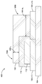
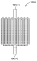
도 1은 수직으로 적층된 집전체 층 및 전극층을 가지는 박막-기반 에너지 저장 장치를 도시한다.
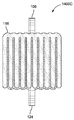
도 2a는 측면으로 인접한 집전체 층 및 전극층을 가지는 에너지 저장 장치의 측면도를 도시한다.
도 2b는 상기 도 2a에 도시된 박막-기반 에너지 저장 장치의 전극층의 평면도를 도시한다.
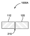
도 3a는 비대칭 측면으로 인접한 집전체 층 및 전극층을 갖는 박막-기반 에너지 저장 장치의 측면도를 도시하되, 상기 제 1 및 제 2 전극층의 표면적의 비는 상기 활성 물질의 몰비에 따라 조절된다.
도 3b는 상기 도 3a에 도시된 박막-기반 에너지 저장 장치의 전극층의 평면도를 도시한다.
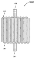
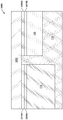
도 4는 측면으로 인접하고 수직 방향으로 오버랩되는 부분을 갖는 집전체 층 및 전극층을 갖는 박막-기반 에너지 저장 장치의 측면도를 도시한다.
도 5는 측면으로 인접한 집전체 층 및 전극층을 갖는 박막-기반 에너지 저장 장치의 측면도를 도시하되, 여기서 상기 전극층은 천공(perforated) 분리부의 대향하는 주요 표면(opposing major surfaces)에 형성되어 상기 박막-기반 에너지 저장 장치의 전체 측면 공간을 늘리지 않고도 향상된 용량을 갖는다.
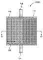
도 6은 도 5에 도시된 박막-기반 에너지 저장 장치의 평면도를 도시한다.
도 7은 수직으로 적층된 집전체 층 및 전극층을 갖는 박막-기반 에너지 저장 장치의 측면도를 도시하며, 여기서 상기 집전체 중 하나는 이들을 관통하여 형성된 천공을 갖고 있으며, 그 위에 형성된 전극층을 갖는 대향하는 주요 표면을 가지어, 상기 박막-기반 에너지 저장 장치의 전체적인 측면 공간을 늘리지 않고도 향상된 용량을 갖는다.
도 8은 수직으로 적층된 집전체 층 및 전극층을 가지는 박막-기반 에너지 저장 장치의 측면도를 도시하며, 여기서 두 층의 제 1 전극층, 두 층의 제 2 전극층 및 두 층의 분리부는 두 에너지 저장 장치가 전기적으로 평행하게 연결되도록 구성되어, 상기 박막-기반 에너지 저장 장치의 전체 측면 공간을 늘리지 않고도 향상된 용량을 갖는다.
도 9는 측면으로 인접한 집전체 층 및 전극층을 갖는 박막-기반 에너지 저장 장치의 측면도를 도시하며, 여기서 상기 집전체 층 및 상기 전극층은 천공 기판의 대향 표면 상에 형성되어, 상기 박막-기반 에너지 저장 장치의 전체 측면 공간을 늘리지 않고도 향상된 용량을 갖는다.
도 10a는 측면으로 인접한 집전체 층 및 전극층을 갖는 박막-기반 에너지 저장 장치의 평면도를 도시하며, 여기서 상기 제 1 및 제 2 전극층은 직사각형 형태를 갖고 측방향으로 오버랩되는 너비를 갖는다.
도 10b는 측면으로 인접한 집전체 층 및 전극층을 갖는 박막-기반 에너지 저장 장치의 전극 배열의 평면도를 도시하며, 여기서 상기 제 1 및 제 2 전극은 직사각형 형태를 갖고 측방향으로 오버랩되는 길이를 갖는다.
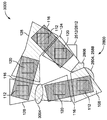
도 10c는 측면으로 인접한 집전체 층 및 전극층을 갖는 박막-기반 에너지 저장 장치의 전극 배열의 평면도를 도시하며, 여기서 각각의 상기 제 1 및 제 2 전극은 규칙적으로 이격된 복수의 직사각형 돌출부(protrusions) 또는 핑거(finger)를 갖고, 상기 제 1 및 제 2 전극의 직사각형 돌출부 또는 핑거는 측방향으로 교번하도록 인터레이스되거나(interlaced) 상호 끼워져서(interleaved), 상기 제 1 및 제 2 전극의 오버랩되는 모서리 길이가 증가한다.
도 10d는 측면으로 인접한 집전체 층 및 전극층을 갖는 박막-기반 에너지 저장 장치의 전극 배열의 평면도를 도시하며, 여기서 각각의 상기 제 1 및 제 2 전극은 규칙적으로 이격된 복수의 둥근(rounded) 돌출부 또는 핑거를 가지며, 상기 제 1 및 제 2 전극의 둥근 돌출부 또는 핑거는 측방향으로 교번하도록 인터레이스되거나 상호 끼워져서, 상기 제 1 및 제 2 전극의 오버랩되는 모서리 길이가 증가한다.
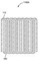
도 10e는 측면으로 인접한 집전체 층 및 전극층을 갖는 박막-기반 에너지 저장 장치의 전극 배열의 평면도를 도시하며, 여기서 각각의 상기 제 1 및 제 2 전극은 규칙적으로 이격된 복수의 장형의(elongated) 돌출부 또는 핑거를 가지며, 여기서 상기 제 1 및 제 2 전극의 장형의 돌출부 또는 핑거는 측방향으로 교번하도록 인터레이스되거나 상호 끼워져서 상기 제 1 및 제 2 전극이 오버랩되는 모서리 길이가 증가한다.
도 11a는 도 10e에 도시된 배열과 유사하게 측면으로 인접한 집전체 층 및 전극층을 갖는 박막-기반 에너지 저장 장치의 전극 배열의 평면도를 도시하며, 여기서 상기 제 1 및 제 2 전극은 거의 같은 표면적을 갖는다.
도 11b는 도 10e에 도시된 배열과 유사하게 측면으로 인접한 집전체 층 및 전극층을 갖는 박막-기반 에너지 저장 장치의 전극 배열의 평면도를 도시하며, 여기서 상기 제 1 및 제 2 전극은 상이한 표면적을 갖고, 상기 제 1 및 제 2 전극층의 표면적 비는 상기 활성 물질의 몰비에 따라 조절된다.
도 12a는 도 10e에 도시된 배열과 유사하게 측면으로 인접한 집전체 층 및 전극층을 가지는 박막-기반 에너지 저장 장치의 제조 중 단계에서 제 1 및 제 2 집전체를 증착한 후의 중간 구조체의 평면도를 도시한 것이다.
도 12b는 도 12a에 도시된 중간 구조체에서 제 1 집전체 상에 제 1 전극층을 증착한 후의 상기 에너지 저장 장치 제조의 이후 단계에서의 중간 구조체의 평면도를 도시한 것이다.
도 12c는 도 12b에 도시된 중간 구조체에 도시된 제 2 집전체 상에 제 2 전극층을 증착한 후의 상기 에너지 저장 장치의 이후 제조 단계에서의 중간 구조체의 평면도를 도시한다.
도 12d는 도 12c에 도시된 중간 구조체에 도시된 제 1 및 제 2 전극층 상에 분리부를 도포한 후의 상기 에너지 저장 장치의 이후 제조 단계에서의 중간 구조체의 평면도를 도시한다.
도 13은 도 10e에 도시된 배열과 유사하게 측면으로 인접한 집전체 층 및 전극층을 갖고, 도 12a-12d에 도시된 제조 공정에 따라 제조된 박막-기반 에너지 저장 장치의 단면도를 도시한다.
도 14a는 각각 규칙적으로 이격된 복수의 장형 돌출부 또는 핑거를 갖는 제 1 및 제 2 집전체를 증착한 후의, 측면으로 인접한 집전체 및 전극을 갖는 박막-기반 에너지 저장 장치의 제조 단계에서의 중간 구조체의 평면도를 도시하며, 여기서 상기 장형 돌출부 또는 핑거는 측방향으로 교번할 수 있도록 인터레이스되거나 상호 끼워져 있다.
도 14b는 도 14a에 도시된 중간 구조체에 도시된 제 1 집전체 상에 제 1 전극층을 증착한 후의, 상기 에너지 저장 장치의 이후 제조 단계에서의 중간 구조체의 평면도를 도시한다.
도 14c는 도 14c에 도시된 중간 구조체에 도시된 제 1 전극층 상에 분리부를 증착한 후의, 상기 에너지 저장 장치의 이후 제조 단계에서의 중간 구조체의 평면도를 도시한다.
도 14d는 도 14c에 도시된 중간 구조체에 도시된 상기 분리부 및 상기 제 2 집전체 상에 제 2 전극층을 증착한 후의, 상기 에너지 저장 장치의 이후 제조 단계에서의 중간 구조체의 평면도를 도시한다.
도 15는 도 14a~14d에 도시된 제조 공정에 따라 제조되고, 수직 방향으로 오버랩되는 부분을 갖고 측면으로 인접한 집전체 층 및 전극층을 갖는 박막-기반 에너지 저장 장치의 단면도를 도시한다.
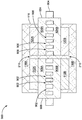
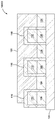
도 16은 측면으로 인접한 집전체 층 및 전극층을 갖는 박막-기반 에너지 저장 장치의 여러 제조 단계에서의 중간 구조체의 평면도를 도시하며, 여기서 상기 에너지 저장 장치는 전기적으로 직렬 연결된 세 단위(units) 또는 셀을 포함한다. 상기 제조 단계는 3 개의 층 단계(layer level)를 형성하는 4회 인쇄 단계(impressions)를 포함한다.
도 17은 측면으로 인접한 집전체 층 및 전극층을 갖는 박막-기반 에너지 저장 장치의 측면도를 도시하며, 여기서 상기 에너지 저장 장치는 도 16에 도시된 제조 공정에 따라서 제조되고, 전기적으로 직렬로 연결된 4개의 단위 또는 셀을 포함한다.
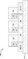
도 18은 측면으로 인접하고 수직 방향으로 오버랩되는 부분을 가지는 집전체 층 및 전극층을 가지는 박막-기반 에너지 저장 장치의 여러 제조 단계에서의 중간 구조체의 평면도를 도시하며, 여기서 상기 에너지 저장 장치는 전기적으로 직렬 연결된 3개의 단위 또는 셀을 포함한다. 상기 제조 단계는 3 개의 층 단계를 형성하는 4회 인쇄 단계를 포함한다.
도 19는 수직 방향으로 오버랩되는 부분을 갖고 측면으로 인접한 집전체 층 및 전극층을 가지는 박막-기반 에너지 저장 장치의 측면도를 도시하며, 여기서 상기 에너지 저장 장치는 도 18에 도시된 제조 방법에 따라서 제조되며, 전기적으로 직렬 연결된 3 개의 단위 또는 셀을 포함한다.
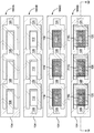
도 20은 측면으로 인접한 집전체 층 및 전극층을 가지는 박막-기반 에너지 저장 장치의 여러 제조 단계에서의 중간 구조체의 평면도를 도시하며, 여기서 각각의 상기 제 1 및 제 2 전극은 규칙적으로 이격된 복수의 직사각형의 돌출부 또는 핑거를 갖고, 여기서 상기 제 1 및 제 2 전극의 직사각형의 돌출부 또는 핑거는 측방향으로 교번하도록 인터레이스되거나 상호 끼워진다. 상기 에너지 저장 장치는 전기적으로 직렬 연결된 2개의 단위 또는 셀을 포함하고, 3개의 층 단계를 형성하는 4회의 인쇄 단계로 제조된다.
도 21은 측면으로 인접한 집전체 층 및 전극층을 가지는 박막-기반 에너지 저장 장치의 여러 제조 단계에서의 중간 구조체의 단면도에 대응하는 평면도를 도시하며, 상기 각각의 제 1 및 제 2 전극은 복수의 동심원으로 구성된다. 상기 에너지 저장 장치는 전기적으로 직렬 연결되고 3개의 층 단계를 형성하는 4회의 인쇄 단계로 제조되는 2개의 단위 또는 셀을 포함한다.
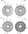
도 22는 측면으로 인접한 집전체 층 및 전극층을 가지는 박막-기반 에너지 저장 장치의 여러 제조 단계에서의 중간 구조체의 평면도를 도시하며, 여기서 상기 각각의 제 1 및 제 2 전극은 규칙적으로 이격된 복수의 장형 돌출부 또는 핑거를 가지는 복수의 동심원으로 구성되고, 상기 제 1 및 제 2 전극의 장형 돌출부 또는 핑거는 원형 방향으로 교번하도록 인터레이스되거나 상호 끼워져서 상기 제 1 및 제 2 전극의 오버랩되는 모서리 길이가 증가한다. 상기 에너지 저장 장치는 전기적으로 직렬 연결된 2 개의 단위 또는 셀을 포함하고, 3 개의 층 단계를 형성하는 4회의 인쇄 단계로 제조된다.
도 23은 박막-기반 에너지 저장 장치와 함께 통합된 웨어러블 박막-기반 전자 장치의 평면도를 도시하며, 여기서 상기 에너지 저장 장치는 전기적으로 직렬 연결된 복수의 단위 또는 셀을 포함한다.
도 24는 바람직한 수의 단위 또는 셀이 변경 가능한(customizable) 전압 및 용량을 위해 전기적으로 직렬 또는 병렬(parallel)로 연결될 수 있도록 천공을 가지는 기판 상에 형성된 단위 또는 셀의 배열을 가지는, 장-구성 가능한(field-configurable) 박막-기반 에너지 저장 장치의 평면도를 도시한다.
도 25는 측면으로 인접한 집전체 층 및 전극층을 갖는 박막-기반 에너지 저장 장치 및 측면으로 배열된 전기 단자(electrical terminals)을 갖는 박막-기반 코어 장치가 내부에 통합되고, 상기 박막-기반 에너지 저장 장치에 의하여 구동되는 통합 박막-기반 전자 장치의 측면도를 도시한다.
도 26은 측면으로 인접한 집전체 층 및 전극층을 가지는 박막-기반 에너지 저장 장치 및 수직으로 배열된 전기 단자를 갖는 박막-기반 코어 장치가 내부에 통합되고 상기 박막-기반 에너지 저장 장치에 의하여 구동되는 통합 박막-기반 전자 장치의 측면도를 도시한다.
도 27은 수직으로 적층된 집전체 층 및 전극층을 갖는 박막-기반 에너지 저장 장치, 수직으로 배열된 전기 단자를 갖는 박막-기반 코어 장치가 내부에 통합되고 상기 박막-기반 에너지 저장 장치에 의하여 구동되는 통합 박막-기반 전자 장치의 측면도를 도시한다.
도 28은 수직으로 배열된 전기 단자를 갖고 본 명세서에 기술된 다양ㅎ산 박막-기반 전자 장치와 함께 통합되고 이에 의하여 전력 공급받도록 구성된 박막-기반 발광 장치를 도시한다.
도 29는 측면으로 인접한 집전체 층 및 전극층을 갖는 박막-기반 에너지 저장 장치, 및 수직으로 배열된 전기 단자를 갖고 상기 박막-기반 에너지 저장 장치에 의하여 구동되는 도 28에 대하여 도시된 상기 박막-기반 발광 장치가 내부에 통합된 통합 박막-기반 전자 장치의 측면도를 도시한다.
도 30은 전기적으로 직렬 연결된 복수의 단위 또는 셀을 포함하는 박막-기반 에너지 저장 장치, 및 수직으로 배열된 전기 단자를 갖고 상기 박막-기반 에너지 저장 장치에 의하여 구동되는 도 28에 대하여 도시된 박막-기반 발광 장치가 내부에 통합된 통합 박막-기반 전자 장치의 위에서 아래로 내려다본 모습(top down view)을 도시한다.
도 31은 전기적으로 직렬 연결되고, 각각의 단위 또는 셀의 각각의 전극이 규칙적으로 이격된 복수의 장형 돌출부 또는 핑거를 갖는 복수의 단위 또는 셀을 포함하는 박막-기반 에너지 저장 장치, 및 수직으로 배열된 전기 단자를 갖고 상기 박막-기반 에너지 저장 장치에 의하여 구동되는 도 28에 대하여 도시된 박막-기반 발광 장치가 내부에 통합된, 통합 박막-기반 전자 장치의 광학 이미지(optical image)의 위에 아래로 내려다본 모습을 도시한다.
도 32는 측면으로 인접한 집전체 층 및 전극층을 갖는 박막-기반 에너지 저장 장치 및 상기 박막-기반 에너지 저장 장치를 충전 모드(charging mode)에서 충전/재충전하도록 구성된 박막-기반 에너지 수집 장치가 내부에 통합된, 통합 박막-기반 전자 장치의 측면도를 도시한다.
도 33은 측면으로 인접한 집전체 층 및 전극층을 가지는 박막-기반 에너지 저장 장치 및 방출(discharge) 모드에서 상기 박막-기반 에너지 저장 장치를 충전/재충전하도록 구성된 박막-기반 에너지 수집 장치가 내부에 통합된, 통합 박막-기반 전자 장치의 측면도를 도시한다.
도 34는 측면으로 인접한 집전체 층 및 전극층을 갖는 박막-기반 에너지 저장 장치 및 상기 박막-기반 에너지 저장 장치를 충전/재충전하도록 구성된 박막-기반 에너지 수집 장치가 내부에 통합된, 통합 박막-기반 전자 장치의 측면도를 도시한다.
도 35는 측면으로 인접한 집전체 층과 전극층 및 건조 분리부, 사용에 앞서 건조 분리부를 적시도록 구성된 별도로 제공되는 전해질을 가지는 박막-기반 에너지 저장 장치를 포함하는, 박막-기반 에너지 저장 장치 제조 키트를 도시한다.These and other features, aspects, and advantages of the invention are described with reference to the drawings of specific embodiments, which are intended to illustrate specific embodiments and not limit the invention. In the drawings, features with reference numbers in parentheses indicate features under other features as viewed by the reader.
1 shows a thin film-based energy storage device having vertically stacked current collector layers and electrode layers.
2A shows a side view of an energy storage device having a current collector layer and an electrode layer adjacent to the side.
FIG. 2B shows a plan view of an electrode layer of the thin film-based energy storage device shown in FIG. 2A.
3A shows a side view of a thin film-based energy storage device having a current collector layer and an electrode layer adjacent to each other in an asymmetric side, wherein the ratio of the surface areas of the first and second electrode layers is adjusted according to the molar ratio of the active material.
3B shows a plan view of an electrode layer of the thin film-based energy storage device shown in FIG. 3A.
4 shows a side view of a thin film-based energy storage device having an electrode layer and a current collector layer having portions adjacent laterally and overlapping in the vertical direction.
5 shows a side view of a thin film-based energy storage device having a current collector layer and an electrode layer adjacent laterally, wherein the electrode layer is formed on the opposing major surfaces of the perforated separating portion and the thin film- The base energy storage device has an improved capacity without increasing the overall side space.
6 shows a plan view of the thin film-based energy storage device shown in FIG. 5.
7 shows a side view of a thin film-based energy storage device having a vertically stacked current collector layer and an electrode layer, wherein one of the current collectors has perforations formed through them, and an opposing electrode layer formed thereon. Having a major surface, it has an improved capacity without increasing the overall side space of the thin film-based energy storage device.
8 shows a side view of a thin film-based energy storage device having a vertically stacked current collector layer and an electrode layer, wherein the two layers of the first electrode layer, the two layers of the second electrode layer and the separation of the two layers are two energy storage devices. Are configured to be electrically connected in parallel, and have an improved capacity without increasing the overall side space of the thin film-based energy storage device.
9 shows a side view of a thin film-based energy storage device having a current collector layer and an electrode layer adjacent to the side, wherein the current collector layer and the electrode layer are formed on opposite surfaces of the perforated substrate, and the thin film-based energy storage It has an improved capacity without increasing the overall side space of the device.
10A shows a plan view of a thin film-based energy storage device having a side-adjacent current collector layer and an electrode layer, wherein the first and second electrode layers have a rectangular shape and a width that overlaps laterally.
FIG. 10B shows a plan view of an electrode arrangement of a thin film-based energy storage device having laterally adjacent current collector layers and electrode layers, wherein the first and second electrodes have a rectangular shape and laterally overlapping lengths.
10C shows a plan view of an electrode arrangement of a thin film-based energy storage device having a current collector layer and an electrode layer adjacent to the side, wherein each of the first and second electrodes is a plurality of regularly spaced rectangular protrusions. Or having a finger, wherein the rectangular protrusions or fingers of the first and second electrodes are interlaced or interleaved so as to alternate in the lateral direction, and the overlapping edge lengths of the first and second electrodes Increases.
10D shows a plan view of an electrode arrangement of a thin film-based energy storage device having a current collector layer and an electrode layer adjacent to the side, wherein each of the first and second electrodes is a plurality of regularly spaced rounded protrusions. Alternatively, a finger is provided, and the round protrusions or fingers of the first and second electrodes are interlaced or interlaced so as to alternate in the lateral direction, so that the length of the overlapping edge of the first and second electrodes is increased.
10E shows a plan view of an electrode arrangement of a thin film-based energy storage device having a current collector layer and an electrode layer adjacent to the side, wherein each of the first and second electrodes is a plurality of regularly spaced elongated electrodes. It has a protrusion or a finger, wherein the elongated protrusions or fingers of the first and second electrodes are interlaced or interlaced so as to alternate in the lateral direction, so that the length of the edge at which the first and second electrodes overlap is increased.
FIG. 11A shows a plan view of an electrode arrangement of a thin film-based energy storage device having laterally adjacent current collector layers and electrode layers similar to the arrangement shown in FIG. 10E, wherein the first and second electrodes have approximately the same surface area. Have.
FIG. 11B shows a plan view of an electrode arrangement of a thin film-based energy storage device having laterally adjacent current collector layers and electrode layers similar to the arrangement shown in FIG. 10E, wherein the first and second electrodes have different surface areas. , The surface area ratio of the first and second electrode layers is adjusted according to the molar ratio of the active material.
12A is a plan view of an intermediate structure after depositing first and second current collectors at a stage during manufacturing of a thin film-based energy storage device having a current collector layer and an electrode layer adjacent to each other in a lateral direction similar to the arrangement shown in FIG. 10E I did it.
12B is a plan view of the intermediate structure in a later step of manufacturing the energy storage device after depositing a first electrode layer on the first current collector in the intermediate structure shown in FIG. 12A.
12C is a plan view of the intermediate structure in a subsequent manufacturing step of the energy storage device after depositing a second electrode layer on the second current collector shown in the intermediate structure shown in FIG. 12B.
12D is a plan view of the intermediate structure in a later manufacturing step of the energy storage device after applying the separation portions on the first and second electrode layers shown in the intermediate structure shown in FIG. 12C.
FIG. 13 shows a cross-sectional view of a thin film-based energy storage device fabricated according to the manufacturing process shown in FIGS. 12A-12D, having laterally adjacent current collector layers and electrode layers similar to the arrangement shown in FIG. 10E.
14A is an intermediate structure in a manufacturing step of a thin film-based energy storage device having a current collector and an electrode adjacent to the side after depositing first and second current collectors having a plurality of elongated protrusions or fingers respectively spaced apart regularly Shows a plan view of, wherein the elongated protrusions or fingers are interlaced or interleaved so as to be alternating laterally.
14B is a plan view of the intermediate structure in a later manufacturing step of the energy storage device after depositing a first electrode layer on the first current collector shown in the intermediate structure shown in FIG. 14A.
14C is a plan view of the intermediate structure in a subsequent manufacturing step of the energy storage device after depositing a separation portion on the first electrode layer shown in the intermediate structure shown in FIG. 14C.
14D is a plan view of an intermediate structure in a subsequent manufacturing step of the energy storage device after depositing a second electrode layer on the separation portion and the second current collector shown in the intermediate structure shown in FIG. 14C.
FIG. 15 is a cross-sectional view of a thin film-based energy storage device manufactured according to the manufacturing process shown in FIGS. 14A to 14D and having a portion overlapping in a vertical direction and having a current collector layer and an electrode layer adjacent to each other in the side.
16 shows a plan view of an intermediate structure at various stages of manufacturing of a thin film-based energy storage device having a current collector layer and an electrode layer adjacent to the side, wherein the energy storage device comprises three units or cells electrically connected in series. Includes. The manufacturing step includes four impressions forming three layer levels.
FIG. 17 shows a side view of a thin film-based energy storage device having a current collector layer and an electrode layer adjacent to the side, wherein the energy storage device is manufactured according to the manufacturing process shown in FIG. 16 and is electrically connected in series. Contains units or cells.
18 shows a plan view of an intermediate structure at various stages of manufacturing a thin film-based energy storage device having a current collector layer and an electrode layer having portions adjacent to the side and overlapping in the vertical direction, wherein the energy storage device is electrically It contains three units or cells connected in series. The manufacturing step includes four printing steps forming a three layer step.
FIG. 19 shows a side view of a thin film-based energy storage device having an overlapping portion in a vertical direction and having a current collector layer and an electrode layer adjacent laterally, wherein the energy storage device is manufactured according to the manufacturing method shown in FIG. , Comprising three units or cells electrically connected in series.
20 shows a plan view of an intermediate structure at various stages of fabrication of a thin film-based energy storage device having a current collector layer and an electrode layer adjacent to the side, wherein each of the first and second electrodes is a plurality of regularly spaced It has rectangular protrusions or fingers, wherein the rectangular protrusions or fingers of the first and second electrodes are interlaced or interleaved so as to alternate laterally. The energy storage device is manufactured in four printing steps comprising two units or cells electrically connected in series, forming three layer steps.
FIG. 21 shows a plan view corresponding to a cross-sectional view of an intermediate structure at various stages of manufacturing of a thin film-based energy storage device having a current collector layer and an electrode layer adjacent to the side, wherein each of the first and second electrodes is a plurality of concentric circles. Consists of The energy storage device comprises two units or cells electrically connected in series and manufactured in four printing steps forming three layer steps.
22 shows a plan view of an intermediate structure at various stages of fabrication of a thin film-based energy storage device having a current collector layer and an electrode layer adjacent to the side, wherein each of the first and second electrodes is a plurality of regularly spaced It is composed of a plurality of concentric circles having elongated protrusions or fingers, and the elongated protrusions or fingers of the first and second electrodes are interlaced or interlaced so as to alternate in a circular direction, thereby increasing the overlapping edge length of the first and second electrodes do. The energy storage device is manufactured in four printing steps comprising two units or cells electrically connected in series and forming three layer steps.
23 shows a plan view of a wearable thin film-based electronic device integrated with a thin film-based energy storage device, wherein the energy storage device includes a plurality of units or cells electrically connected in series.
Figure 24 is a long-configuration, with an arrangement of units or cells formed on a substrate with perforations such that a desired number of units or cells can be electrically connected in series or parallel for a customizable voltage and capacity. Shows a top view of a field-configurable thin film-based energy storage device.
25 is a thin film-based energy storage device having a current collector layer and an electrode layer adjacent to the side and a thin film-based core device having electrical terminals arranged laterally are integrated therein, the thin film-based energy storage device Shows a side view of an integrated thin film-based electronic device driven by.
26 is a thin film-based energy storage device having a current collector layer and an electrode layer adjacent to the side and a thin film-based core device having vertically arranged electrical terminals are integrated therein and driven by the thin film-based energy storage device A side view of a thin film-based electronic device is shown.
27 is a thin film-based energy storage device having a vertically stacked current collector layer and an electrode layer, a thin film-based core device having vertically arranged electrical terminals is integrated therein and driven by the thin film-based energy storage device Shows a side view of an integrated thin film-based electronic device.
28 shows a thin film-based light emitting device configured to have vertically arranged electrical terminals and to be integrated with and powered by various thin film-based electronic devices described herein.
FIG. 29 is a thin film-based energy storage device having a current collector layer and an electrode layer adjacent to the side and the thin film-based energy storage device shown with respect to FIG. 28 having vertically arranged electrical terminals and driven by the thin film-based energy storage device. Shows a side view of an integrated thin film-based electronic device in which the light emitting device is integrated.
FIG. 30 is a thin film-based energy storage device comprising a plurality of units or cells electrically connected in series, and a thin film shown with respect to FIG. 28 having vertically arranged electrical terminals and driven by the thin film-based energy storage device. It shows a top down view of an integrated thin film-based electronic device with the base light emitting device integrated therein.
31 is a thin film-based energy storage device comprising a plurality of units or cells electrically connected in series and having a plurality of elongated protrusions or fingers in which each electrode of each unit or cell is regularly spaced, and vertically arranged The thin film-based light emitting device shown with respect to FIG. 28, which has an electrical terminal and is driven by the thin film-based energy storage device, is integrated inside, on top of the optical image of the integrated thin film-based electronic device. Show the look down.
32 is a thin film-based energy storage device having a current collector layer and an electrode layer adjacent to the side and a thin film-based energy collection device configured to charge/recharge the thin film-based energy storage device in a charging mode are integrated therein Shows a side view of the integrated thin film-based electronic device.
33 is a thin film-based energy storage device having a current collector layer and an electrode layer adjacent to the side and a thin film-based energy collection device configured to charge/recharge the thin film-based energy storage device in a discharge mode are integrated therein. , Shows a side view of an integrated thin film-based electronic device.
Figure 34 is a thin film-based energy storage device having a current collector layer and an electrode layer adjacent to the side and a thin film-based energy collection device configured to charge/recharge the thin film-based energy storage device are integrated therein, integrated thin film-based electronics Shows a side view of the device.
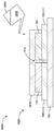
Figure 35 is a thin film-based energy storage device manufacturing kit comprising a thin film-based energy storage device having a separately provided electrolyte configured to wet the dry separator prior to use, the current collector layer and the electrode layer and the dry separator adjacent to the side. Shows.
[모든 우선권 출원의 참조를 통한 병합][Merge by reference of all priority applications]
본 출원과 함게 제출된 출원 데이터 시트에서 외국 또는 국내 우선권 주장이 확인된 모든 출원은 모든 목적을 위해 전체적으로 참조로 병합된다.All applications for which a foreign or domestic priority claim has been identified in the application data sheet filed with this application are incorporated by reference in their entirety for all purposes.
[발명의 상세한 설명][Detailed description of the invention]
특정 구현예와 실시예가 아래 서술되어 있지만, 통상의 기술자는 본 발명이 구체적으로 개시된 구현예 및/또는 사용예와 이들의 명백한 수정, 균등물 이상으로 확장될 수 있다는 점을 이해할 수 있을 것이다. 따라서, 여기 개시된 본 발명의 범위는 아래 기재된 어떠한 특정 구현예로도 제한되지 않는 것으로 의도되는 것이다.While specific embodiments and examples are described below, one of ordinary skill in the art will appreciate that the present invention may be extended beyond the specifically disclosed embodiments and/or usage examples and their apparent modifications and equivalents. Accordingly, it is intended that the scope of the invention disclosed herein is not limited to any specific embodiments described below.
본 명세서에 기술된 것과 같이, 인쇄 또는 적층(additive) 제조는 재료가 층 단위로(layer-by-layer fashion) 축적(accumulated), 성장 또는 질량이 증가하여 2차원 또는 3차원 물체를 형성하는 공정을 의미한다. 첨가되는 재료는 액체 및/또는 고체일 수 있다. 상기 물체는 기판과 같이 존재하는 구성(component)에 추가 또는 결합될 수 있다.As described herein, printing or additive manufacturing is a process in which a material is accumulated in a layer-by-layer fashion, grown, or increased in mass to form a two-dimensional or three-dimensional object. Means. The material to be added can be liquid and/or solid. The object can be added to or coupled to an existing component such as a substrate.
일반적으로, 전자 장치를 인쇄하여 제조하는 것이 다른 기술에 대하여 가지는 강점은 예를 들어, 복잡한 형상 형성과의 호환성, 향상된 폼 팩터(form factor), 감소된 전체 두께, 감소된 장치의 차지 공간(footprint), 예컨대 박막-기반 장치 같은 른 장치와의 통합 용이성, 가요성, 비용의 절감, 대면적 구조의 형성, 대량 생산, 낮은 원가 및 롤투롤(roll-to-roll) 제조와 같은 기타 고처리량 제조 공정과의 결합 가능성을 포함한다.In general, the advantages of printing and manufacturing electronic devices over other technologies are, for example, compatibility with complex shape formation, improved form factor, reduced overall thickness, and reduced device footprint. ), e.g. ease of integration with other devices such as thin film-based devices, flexibility, cost reduction, formation of large area structures, mass production, low cost and other high throughput manufacturing such as roll-to-roll manufacturing Includes the possibility of combining with the process.
본 명세서에 기술된 바와 같이, 인쇄된 장치는 인쇄 공정을 사용하여 인쇄된 적어도 한 층 또는 구성을 가지거나, 인쇄 공정을 사용하여 인쇄된 복수의 구성 또는 층을 가지거나, 인쇄 공정을 사용하여 인쇄된 모든 구성 또는 층을 가지는 장치를 나타낸다.As described herein, a printed device may have at least one layer or configuration printed using a printing process, or have a plurality of configurations or layers printed using a printing process, or printed using a printing process. Represents a device having all configurations or layers.
본 명세서에 기술된 다양한 구현예에서, 유리한 것으로 기술된 다양한 장치 및 기구(apparatuses)의 적어도 한 구성은 박막 구성을 포함할 수 있다. 하나 이상의 박막 구성은 인쇄된 구성일 수 있다. 본 명세서에 기술된 바와 같이, 박막 구성을 형성하기 위한 적합한 인쇄 공정은 기타 적합한 인쇄 공정 가운데 그라비어 인쇄(gravure printing), 스크린 프린팅(screen printing), 리소그래피(lithography), 플렉소그래피(flexography), 잉크젯 프린팅(ink-jet pringting), 회전 스크린 프린팅(rotary screen printing) 및 스텐실(stenciling)을 포함한다. 이들 인쇄 공정 중 하나 이상은 예컨대 롤투롤 공정과 같은 다른 고부피(high volume) 제조 기술과 결합될 수 있다. 장치의 부품 또는 구성을 인쇄하는 것은 예를 들어 감소된 두께, 작은 크기(compact dimensions) 및 적은 폐기물과 같은 다양한 이점을 제공할 수 있다. 인쇄된 장치는 또한 상기 인쇄된 장치 또는 그 구성 요소의 적층(stacking)을 다른 것들 가운데 가능하게 함으로써 상기 장치의 주어진 공간에서의 기능성을 향상시킬 수 있다. 다른 공정을 사용하여 제조된 장치와 다르게, 일부 인쇄된 장치는 또한 유연하여(flexible) 기타 장치들 가운데 웨어러블 의료 장치, 디스플레이, 센서, 스마트카드, 스마트 패키징, 스마트 의류, 간판, 광고와 같은 웨어러블 장치에 적합할 수 있다.In the various embodiments described herein, at least one configuration of the various devices and apparatuses described as advantageous may comprise a thin film configuration. The one or more thin film configurations may be printed configurations. As described herein, suitable printing processes for forming thin film configurations include gravure printing, screen printing, lithography, flexography, inkjet, among other suitable printing processes. Including ink-jet pringting, rotary screen printing and stenciling. One or more of these printing processes may be combined with other high volume manufacturing techniques such as, for example, a roll-to-roll process. Printing parts or configurations of the device can provide various advantages, such as reduced thickness, compact dimensions and less waste, for example. Printed devices can also enhance the functionality of the device in a given space by enabling the stacking of the printed device or its components, among others. Unlike devices manufactured using other processes, some printed devices are also flexible, so wearable devices such as wearable medical devices, displays, sensors, smart cards, smart packaging, smart clothing, signs, advertisements, among others. May be suitable for
다양한 구현 예에 따르면, 박막-기반 에너지 저장 장치(ESD)는 기판 상에 형성된 전기적으로 분리된 집전체 층을 포함한다. 상기 집전체 층은 상기 ESD의 음극 또는 양극의 하나를 구성할 수 있는 제 1 유형의 제 1 집전체 층, 및 상기 ESD의 음극 또는 양극 중 다른 하나를 구성할 수 있는 제 2 유형의 제 2 집전체 층을 포함한다. 상기 제 1 및 제 2 집전체 층은 예를 들어 인쇄 방식으로 상기 기판의 공통 표면 상에(over or on) 증착될 수 있다. 상기 ESD는 상기 제 1 유형의 제 1 집전체 층 상에(over or on) 예를 들어 인쇄 방식으로 형성된, 예를 들어 음극 또는 양극의 층과 같은 제 1 유형의 제 1 전극층을 추가적으로 포함한다. 상기 ESD는 상기 제 2 유형의 제 2 집전체 층 상에(over or on) 예를 들어 인쇄 방식으로 형성된, 예를 들어 음극 또는 양극 중 다른 것의 층과 같은 제 2 유형의 제 2 전극층을 추가적으로 포함한다. 상기 ESD는 또한 상기 제 1 전극층 및 상기 제 2 전극층 중 하나 또는 둘 모두 상에 형성된, 예를 들어 인쇄된 분리부인 분리부를 포함한다.According to various embodiments, a thin film-based energy storage device (ESD) includes an electrically separated current collector layer formed on a substrate. The current collector layer is a first type of first current collector layer capable of constituting one of the cathode or anode of the ESD, and a second type of second current collector layer capable of constituting the other of the cathode or anode of the ESD. Includes the entire layer. The first and second current collector layers may be deposited over or on a common surface of the substrate by, for example, a printing method. The ESD further comprises a first type of first electrode layer, for example a layer of a cathode or an anode, formed over or on the first current collector layer of the first type, for example by printing. The ESD additionally comprises a second electrode layer of a second type, for example a layer of another one of a negative electrode or a positive electrode, formed, for example by printing, on the second current collector layer of the second type (over or on). do. The ESD also includes a separator formed on one or both of the first electrode layer and the second electrode layer, for example a printed separator.
본 명세서에 개시된 바와 같이, 박막-기반 ESD는 1차 전지, 2차 전지, 슈퍼커패시터(supercapacitor) 및 전지-슈퍼커패시터 하이브리드 장치 중 하나 이상을 포함할 수 있다. 상기 ESD가 1차 전지를 포함할 때, 상기 ESD는 예를 들어 아연/탄소, 아연/알칼리/망간, 마그네슘/망간 디옥사이드, 아연/산화수은, 카드뮴/산화수은, 아연/산화은, 아연/공기, 리튬/용해성 양극 및 리튬/고체 양극 1차 전지로서 구성될 수 있다. 상기 ESD가 2차 전지를 포함할 때, 상기 ESD는 예를 들어, 니켈/철, 은/철, 은/공기, 니켈/카드뮴, 니켈/금속 하이브리드, 니켈/아연, 아연/산화은, 리튬이온, 리튬/금속, Zn/MnO2, 아연/공기, 알루미늄/공기, 마그네슘/공기, 및 리튬/공기/리튬/폴리머 2차 전지로 구성될 수 있다.As disclosed herein, a thin film-based ESD may include one or more of a primary battery, a secondary battery, a supercapacitor, and a battery-supercapacitor hybrid device. When the ESD includes a primary battery, the ESD includes, for example, zinc/carbon, zinc/alkali/manganese, magnesium/manganese dioxide, zinc/mercury oxide, cadmium/mercury oxide, zinc/silver oxide, zinc/air, lithium/ It can be configured as a soluble positive electrode and a lithium/solid positive electrode primary battery. When the ESD includes a secondary battery, the ESD includes, for example, nickel/iron, silver/iron, silver/air, nickel/cadmium, nickel/metal hybrid, nickel/zinc, zinc/silver oxide, lithium ion, Lithium/metal, Zn/MnO 2 , zinc/air, aluminum/air, magnesium/air, and lithium/air/lithium/polymer secondary batteries.
일부 구현예에서, 박막-기반 ESD는 두 전극 모두 이중층(double-layer) 커패시터로 구성된 슈퍼커패시터, 두 전극 모두 슈도커패시터(pseudo capacitor), 또는 한 전극은 이중층이고 다른 전극은 슈도커패시터로 구성된 것을 포함할 수 있다.In some embodiments, thin-film-based ESD includes supercapacitors in which both electrodes are composed of double-layer capacitors, both electrodes are composed of pseudo capacitors, or one electrode is a double layer and the other electrode is composed of a pseudocapacitor. can do.
일부 구현예(implementations)에서, 상기 박막-기반 ESD는 대칭 인쇄 전극을 가지는 슈퍼커패시터를 포함할 수 있으며, 여기서 각각의 전극은, 예를 들어 산화아연(ZnxOy) 또는 산화망간(MnxOy)을 포함한다. 다른 구현예에서, 상기 박막-기반 ESD는 대칭 인쇄 전극을 가지는 슈퍼커패시터를 포함할 수 있으며, 여기서 각각의 전극은 그 위에 탄소나노튜브가 형성된 것이다. 일부 구현예에서, 상기 박막-기반 ESD는 비대칭 인쇄 전극을 가지는 슈퍼커패시터를 포함할 수 있으며, 여기서 전극 중 하나는, 예를 들어 산화아연(ZnxOy) 또는 산화망간(MnxOy)을 포함할 수 있고, 다른 전극은 탄소나노튜브를 포함할 수 있다.In some implementations, the thin-film-based ESD may include a supercapacitor having symmetric printed electrodes, where each electrode is, for example, zinc oxide (Zn x O y ) or manganese oxide (Mn x O y ). In another embodiment, the thin-film-based ESD may include a supercapacitor having a symmetrical printed electrode, wherein each electrode has a carbon nanotube formed thereon. In some embodiments, the thin film-based ESD may include a supercapacitor having an asymmetric printed electrode, wherein one of the electrodes is, for example, zinc oxide (Zn x O y ) or manganese oxide (Mn x O y ) It may include, and the other electrode may include a carbon nanotube.
본 명세서에 개시된 바와 같이, 때로는 울트라커패시터, 전기 이중층 커패시터(electric double layer capacitors, EDLC) 또는 전기화학 커패시터(electrochemical capacitors)라 지칭되는 슈퍼커패시터는 비교적 새로운 에너지 저장 장치로서, 그 특성이 유리하게는 일부 측면에서는 종래의 정전기적 커패시터(electrostatic capacitors)와 유사하지만, 다른 측면에서는 종래의 전지, 예를 들어 이차 전지와 유사하다.As disclosed herein, supercapacitors, sometimes referred to as ultracapacitors, electric double layer capacitors (EDLC) or electrochemical capacitors, are relatively new energy storage devices, and their properties are advantageously some In terms of which it is similar to conventional electrostatic capacitors, in other aspects, it is similar to a conventional battery, for example, a secondary battery.
특정 전지와 유사하게, 슈퍼커패시터는 다공성 분리부 및 전해질에 의하여 분리된 양극(cathode or a positive electrode) 및 음극(anode or a negative electrode)를 가진다. 예를 들어, 상기 분리부는 이온 투과성이고 전해질에 침지된(soaked) 유전 물질을 포함할 수 있다. 전지의 충전 또는 방전 중에 전기화학 반응의 일부로서 한 전극에서 다른 전극으로 일어나는 이온 전달(ion transport)는 슈퍼커패시터에서는 일어나지 않는다.Similar to certain cells, supercapacitors have a porous separator and a cathode or a positive electrode and an anode or a negative electrode separated by an electrolyte. For example, the separator may include a dielectric material that is ion permeable and soaked in an electrolyte. Ion transport from one electrode to another as part of the electrochemical reaction during charging or discharging of the cell does not occur in the supercapacitor.
슈퍼커패시터는, 예를 들어 비교적 빠른 충전 능력(capability)과 같이 일부 측면에서 종래의 정전기적 커패시터와 유사하지만, 종래의 정전기적 커패시터와 비교하여 현저히 높은 충전 용량을 갖는다. 에너지를 유전체(dielectric)로 분리된 전극에 저장하는 종래의 정전기적 커패시터와 다르게, 슈퍼커패시터는 에너지를 양극과 전해질 사이의 계면 및 음극과 전해질 사이의 계면 중 하나 또는 둘 모두에 에너지를 저장한다.Supercapacitors are similar to conventional electrostatic capacitors in some respects, for example relatively fast charging capability, but have a significantly higher charging capacity compared to conventional electrostatic capacitors. Unlike conventional electrostatic capacitors that store energy in electrodes separated by a dielectric, supercapacitors store energy at one or both of the interface between the anode and the electrolyte and the interface between the cathode and the electrolyte.
슈퍼커패시터의 충전 용량(capacitance) 값은 종래의 정전기적 커패시터보다 현저히 높을 수 있다. 일부 슈퍼커패시터는 종래의 정전기적 커패시터와 비교하여 낮은 전압 한계(voltage limits)를 갖는다. 예를 들어, 일부 슈퍼커패시터는 작동을 위해 2.6~2.8 V로 제한된다. 일부 슈퍼커패시터는 2.8V 또는 그 이상의 전압에서 작동할 수 있다. 어떤 슈퍼커패시터는 감소된 이용 수명(service life)를 나타낸다.The charging capacity of the supercapacitor may be significantly higher than that of a conventional electrostatic capacitor. Some supercapacitors have lower voltage limits compared to conventional electrostatic capacitors. For example, some supercapacitors are limited to 2.6 to 2.8 V for operation. Some supercapacitors can operate at a voltage of 2.8V or higher. Some supercapacitors exhibit a reduced service life.
슈퍼커패시터는 일반적으로 전지보다 현저히 높은 전력 밀도를 갖는데, 이는 이들이 전지보다 매우 빠르게 전하를 전달할 수 있기 때문이다. 슈퍼커패시터는 일반적으로 전지와 비교하여 현저히 낮은 내부 저항(internal resistance)을 갖고, 결과적으로, 급속 충/방전 시 열이 덜 발생한다. 일부 슈퍼커패시터는 수백만 회 충전 및 방전될 수 있으나, 많은 이차 전지는 500~10000회로 현격하게 짧은 전형적인 수명을 갖는다. 일부 슈퍼커패시터는 전지와 비교하여 매우 낮은 에너지 밀도를 갖는다. 어떤 상용(commercial) 슈퍼커패시터는 상용 전지에 비하여 비싸다(와트당 높은 가격).Supercapacitors generally have a significantly higher power density than cells because they can transfer charge much faster than cells. Supercapacitors generally have a significantly lower internal resistance compared to batteries, and as a result, less heat is generated during rapid charging/discharging. Some supercapacitors can be charged and discharged millions of times, but many secondary batteries have a typical lifespan that is significantly short of 500-10000 cycles. Some supercapacitors have a very low energy density compared to cells. Some commercial supercapacitors are expensive (higher price per watt) compared to commercial cells.
이러한 특성 및 다른 특성 때문에, 슈퍼커패시터는 많은 급속 충전/방전 사이클이 장기간의 에너지 저장보다 더 필요한 분야(applications)에서 사용된다. 예를 들어, 큰 단위의 슈퍼커패시터의 응용 분야는 예를 들어 자동차, 버스, 기차, 크레인 및 엘리베이터를 포함하고, 여기서, 이들은 회생 제동(regenerative braking), 단기 에너지 저장 또는 버스트 모드 전력 공급(power delivery)에 사용된다. 작은 단위의 슈퍼커패시터의 응용 분야는 정적 임의 접근 메모리(static random-access memory, SRAM)를 위한 메모리 백업을 포함한다. 기타 현재 또는 미래의 슈퍼커패시터 응용 분야는 휴대전화, 노트북, 전기차 및 전지를 사용하는 다른 다양한 장치를 포함하는 다양한 소비자 전자 장치를 포함한다. 이들이 전지와 비교하여 현저히 빠르게 재충전될 수 있기 때문에, 슈퍼커패시터는 특히 예를 들어 현재의 전기차 또는 휴대전화가 충전하는 데 소비하는 시간(hours) 단위 대신 분(minutes) 단위의 빠른 충전 속도가 이점이 되는 장치들에 매력적이다.Because of these and other properties, supercapacitors are used in applications where many fast charge/discharge cycles are more than long-term energy storage. For example, applications of large unit supercapacitors include, for example, automobiles, buses, trains, cranes and elevators, where they are regenerative braking, short-term energy storage or burst mode power delivery. ). Applications of small-scale supercapacitors include memory backup for static random-access memory (SRAM). Other current or future supercapacitor applications include a variety of consumer electronic devices, including cell phones, notebooks, electric vehicles, and a variety of other devices that use batteries. Because they can be recharged significantly faster compared to batteries, supercapacitors in particular benefit from a fast charging rate in minutes instead of the hours that a current electric vehicle or mobile phone spends charging, for example. It is attractive to the devices that become.
일부 장치에 있어서, 슈퍼커패시터는, 슈퍼커패시터와 전지의 장점을 모두 취할 수 있도록 전지와 함께 쓰인다. 이러한 응용 분야에서, 슈퍼커패시터는 단기간의 전력 수요를 채우기 위하여 빠른 충전이 필요할 때 사용되는 반면에, 전지는 장기간의 에너지 공급을 위하여 사용된다. 이 둘을 하이브리드 에너지 저장 장치로 결합하는 것은 두 수요를 모두 충족할 수 있고 동시에 전지의 응력(stress)을 감소시킬 수 있고, 그에 따라서 전지와 슈퍼커패시터의 이용 수명을 증가시킬 수 있다.In some devices, a supercapacitor is used with a battery to take advantage of both the supercapacitor and the battery. In these applications, supercapacitors are used when fast charging is required to meet short-term power demand, while batteries are used for long-term energy supply. Combining the two into a hybrid energy storage device can meet both demands and at the same time reduce the stress of the battery, thus increasing the useful life of the battery and supercapacitor.
어떤 이론에도 얽매이지 않고, 슈퍼커패시터는 전기 이중층 커패시턴스 및/또는 슈도커패시턴스을 포함하는 다른 메커니즘으로 에너지를 저장할 수 있다. 이중층 커패시턴스는 정전기적 특성을 가지는 반면에, 슈도커패시턴스는 전기화학적 특성을 가진다. 상기 다른 메커니즘은 더 자세하게 후술된다. 상기 저장 메커니즘이 이중층 커패시턴스 특성 및/또는 슈도커패시턴스 특성을 가지는지에 따라서, 그리고 상기 상기 슈퍼커패시터가 두 개의 동일 또는 대칭 전극을 가지는지 두 개의 상이 또는 비대칭 전극을 가지는지에 따라서, 슈퍼커패시터는 몇 가지 구현예에 따른 세 개의 구분되는 슈퍼커패시터 그룹 중 하나로 구성될 수 있다.Without wishing to be bound by any theory, supercapacitors can store energy with other mechanisms including electric double layer capacitance and/or pseudocapacitance. The double layer capacitance has electrostatic properties, whereas the pseudo capacitance has electrochemical properties. These other mechanisms will be described in more detail later. Depending on whether the storage mechanism has a double layer capacitance characteristic and/or a pseudocapacitance characteristic, and whether the supercapacitor has two identical or symmetrical electrodes or two different or asymmetrical electrodes, how many supercapacitors It may be configured as one of three distinct supercapacitor groups according to different implementations.
슈퍼커패시터의 첫번째 그룹은 두 전극 모두 슈도커패시터로 구성되어 있으며, 여기서 각각의 전극은 전이 금속 옥사이드(예를 들어, 망간 옥사이드 또는 아연 옥사이드)을 포함하고, 슈도 커패시턴스(pseudo capacitance)를 갖도록 구성되어 있다. 예를 들어, 상기 금속 산화물은 나노 구조체의 형태를 하고 있을 수 있다. 슈퍼커패시터의 두번째 그룹은 두 전극 모두 EDLC로 구성되어 있고, 여기서 각각의 전극은 탄소(예를 들어 탄소 나노튜브)를 포함하고, 이중층 커패시턴스를 갖도록 구성되어 있다. 슈퍼커패시터의 세번째 그룹은 하이브리드 슈퍼커패시터로도 칭할 수 있으며, EDLC로 구성된 하나의 전극과 슈도커패시터로 구성된 다른 전극을 갖는다. 하이브리드 커패시터의 일부로 포함될 때, 상기 슈도커패시터로 구성된 전극은 양극 또는 양전하를 띤 전극으로 기능할 수 있고, EDLC로 구성된 전극은 음극 또는 음전하를 띤 전극으로 기능할 수 있다.In the first group of supercapacitors, both electrodes are composed of pseudocapacitors, where each electrode contains a transition metal oxide (e.g., manganese oxide or zinc oxide), and is configured to have a pseudo capacitance. . For example, the metal oxide may be in the form of a nanostructure. The second group of supercapacitors is composed of both electrodes of EDLC, where each electrode contains carbon (eg carbon nanotubes) and is configured to have a double layer capacitance. The third group of supercapacitors, which can also be referred to as hybrid supercapacitors, has one electrode composed of EDLC and another electrode composed of pseudocapacitor. When included as a part of a hybrid capacitor, an electrode composed of the pseudocapacitor may function as an anode or a positively charged electrode, and an electrode composed of an EDLC may function as a cathode or a negatively charged electrode.
다양한 구현예에 따라 제조된 상기 ESD는 많은 이점이 있다. 예를 들어, 박막-기반 ESD의 일부 성능 지표(performance metrics)는 상기 ESD의 여러 층들의 두께에 따라 달라질 수 있다. 상기 ESD의 여러 층들의 두께는 상기 층들을 형성하는 데 사용되는(employed) 증착 기술에 의하여 제한될 수 있다. 예를 들어, 일부 박막-기반 ESD의 용량은 전극 활성 물질을 포함하는 전극층의 두께에 의하여 제한될 수 있다. 필름 응력 및/또는 계면(interfacial) 에너지로부터 야기되는 층의 균열(cracking) 및/또는 박리(delaminating)로 인해, 상기 ESD의 용량은 안정적으로 증착될 수 있는 전극층의 두께에 의하여 제한될 수 있다. 인쇄에 의하여, 상기 ESD의 하나 이상의 층들 중 비교적 두꺼운 층이 얻어질 수 있다. 예를 들어, 본 명세서에 기술된 다양한 실시예로 기술된 것과 같이, 전기적으로 연결된 인쇄층은 구성(feature)의 다중 표면에 형성되고, 서로의 위에 적층될 수 있다. 따라서, 다양한 구조적 특징 및 본 명세서에 기술된 인쇄 방법을 포함하는 제조 방법을 사용함으로써, 본 명세서에 개시된 구현예에 따른 박막-기반 ESD는 다른 장점 중에서도 높은 용량을 가질 수 있다. The ESD manufactured according to various embodiments has many advantages. For example, some performance metrics of thin-film-based ESD may depend on the thickness of the different layers of the ESD. The thickness of the various layers of the ESD can be limited by the deposition technique employed to form the layers. For example, the capacity of some thin film-based ESD can be limited by the thickness of the electrode layer including the electrode active material. Due to the cracking and/or delaminating of the layer resulting from film stress and/or interfacial energy, the capacity of the ESD may be limited by the thickness of the electrode layer that can be stably deposited. By printing, a relatively thick layer of one or more layers of the ESD can be obtained. For example, as described in the various embodiments described herein, electrically connected printed layers are formed on multiple surfaces of a feature and can be stacked on top of each other. Thus, by using a manufacturing method including various structural features and the printing method described herein, the thin film-based ESD according to the embodiments disclosed herein can have a high capacity among other advantages.
본 명세서에서 사용된 바와 같이, 전극 활성 물질은 화학적으로 에너지 저장 메커니즘과 관련된 전극 구성 요소를 지칭한다. 예를 들어, 전지에서, 전극 활성 물질은 전기화학적 충전 또는 방전 반응에 참여하는 양극 또는 음극 성분이다. 슈퍼커패시터에서, 전극 활성 물질은 이중층 커패시턴스(EDLC) 또는 전기화학 슈도커패시턴스에 참여하는 양극 또는 음극 성분이다.As used herein, electrode active material refers to an electrode component chemically associated with an energy storage mechanism. For example, in a battery, the electrode active material is a positive or negative component that participates in an electrochemical charge or discharge reaction. In supercapacitors, the electrode active material is an anode or cathode component that participates in double layer capacitance (EDLC) or electrochemical pseudocapacitance.
박막-기반 ESD의 하나 이상의 층을 인쇄하는 것은 상기 ESD의 작동 전류 및/또는 저항을 필요에 맞게 조정하는 것(customization)을 가능하게 한다. 예를 들어, 부분적으로는 인쇄가 더 높은 수준으로 개별 층(individual layers)의 형태 및 두께를 필요에 맞게 조정하는 것을 가능하게 하여 상기 ESD 장치의 전기화학 반응에 필요한 전극의 표면적을 더 쉽게 조정할 수 있다. 상기 박막-기반 ESD의 하나 이상의 층을 인쇄하는 것은 복수의 ESD 단위와 셀을 상기 ESD의 전압 및/또는 용량을 조절하기 위하여 전기적으로 직렬 및/또는 병렬로 연결되는 것을 가능하게 한다. Printing one or more layers of thin-film-based ESD makes it possible to customize the operating current and/or resistance of the ESD to suit needs. For example, in part, printing makes it possible to adjust the shape and thickness of the individual layers to a higher level to suit your needs, making it easier to adjust the surface area of the electrodes required for the electrochemical reaction of the ESD device. have. Printing one or more layers of the thin-film-based ESD enables a plurality of ESD units and cells to be electrically connected in series and/or parallel to regulate the voltage and/or capacity of the ESD.
상기 박막-기반 ESD의 하나 이상의 층을 인쇄하는 것은 또한 상기 박막-기반 ESD를 통합한 다양한 박막-기반 장치들의 전체 두께 및/또는 차지 부피(footprint)의 감소를 가능하게 한다. 이는 부분적으로는 인쇄가 개별 층의 형태 및 두께를 높은 수준으로 조정하는 것을 가능하게 하기 때문이다.Printing one or more layers of the thin-film-based ESD also makes it possible to reduce the overall thickness and/or footprint of various thin-film-based devices incorporating the thin-film-based ESD. This is in part because printing makes it possible to adjust the shape and thickness of the individual layers to a high level.
상기 박막-기반 ESD의 하나 이상의 층을 인쇄하는 것은 또한 전체 공정 단계 수를 감소할 수 있다. 예를 들어, 감산 패터닝(subtractive patterning) 기술에 적용되는 하나 이상의 마스킹(masking) 단계는 하나 이상의 층을 인쇄함으로써 생략될 수 있다. 또한, 상이한 층을 측면으로 및/또는 동시에 인쇄함으로써 전체 공정 단계 수는 감소될 수 있다.Printing one or more layers of the thin film-based ESD can also reduce the total number of process steps. For example, one or more masking steps applied in a subtractive patterning technique may be omitted by printing one or more layers. Further, by printing different layers laterally and/or simultaneously, the total number of process steps can be reduced.
상기 박막-기반 ESD의 하나 이상의 층을 인쇄하는 것은 또한 상기 ESD에 의하여 구동되는 박막-기반 전자 장치와의 높은 수준의 통합을 가능하게 한다. 이것은 상기 ESD 및 상기 ESD에 의하여 구동되는 전자 장치를 인쇄하는 데 유사한 물질이 사용되기 때문일 수 있다. 상기 ESD의 일부 층 및 상기 전자 장치는 심지어 동시에 인쇄될 수도 있다.Printing one or more layers of the thin-film-based ESD also enables a high level of integration with thin-film-based electronic devices driven by the ESD. This may be because a similar material is used to print the ESD and the electronic device driven by the ESD. Some layers of the ESD and the electronic device may even be printed simultaneously.
본 명세서에 기술된 바와 같이, 다양한 구현예에서, 상기 ESD의 일부 층이 인쇄되는 반면에, 다른 구현 예에서, 상기 ESD의 모든 층이 인쇄된다. 인쇄되지 않는 층들은 도금(plating), 증발(evaporation), 스퍼터링(sputtering), 화학 기상 증착(chemical vapor deposition) 또는 다른 임의의 박막 증착 기술을 포함하는 적절한 방법으로 증착될 수 있다.As described herein, in various embodiments, some layers of the ESD are printed, while in other embodiments, all layers of the ESD are printed. Non-printing layers may be deposited by any suitable method including plating, evaporation, sputtering, chemical vapor deposition or any other thin film deposition technique.
박막-기반 에너지 저장 장치에서의 수직 적층 대 측면 인접 전극 구성Vertical stacking vs. side adjacent electrode configuration in thin film-based energy storage devices
일반적으로, 박막-기반 에너지 저장 장치(EDSs), 예를 들어, 인쇄된 ESD는, 집전체 층 및/또는 전극층의 상대적인 방향에 따라 분류될 수 있다. 첫번째 ESD 분류(category)는 수직으로 적층된 집전체 층 및 전극층을 가지는 박막-기반 에너지 저장 장치를 포함하며, 두번째 ESD 분류는 측면으로 인접한 집전체 층 및 전극층을 가지는 박막-기반 에너지 저장 장치를 포함한다. 두 ESD 분류 모두 기판 상에 완전히 인쇄될 수 있고, 이는 집전체 및/또는 전극이 예를 들어 상이한 기판 상에서 각각 형성되고 이어서 이들 사이에 배치된 분리부와 이들을 접합(adjoining)한 ESD와 비교하여, 상술한 다양한 이점을 제공한다. 기판의 동일 측 상에서 측면으로 인접한 집전체를 가지는 본 명세서에 기술된 다양한 구현예에 따른 ESD는 동일한 기판 상에서 다른 장치와 통합되는 데 유리하며, 이는 적어도 전기적 연결이 예를 들어 통합된 장치의 전도성 리드(conductive leads)로 연장되거나(extend into) 또는 이에 접촉하는 집전체를 인쇄함으로써 용이하게 만들어질 수 있기 때문이다.In general, thin film-based energy storage devices (EDSs), eg, printed ESDs, can be classified according to the relative orientation of the current collector layer and/or electrode layer. The first ESD category includes thin-film-based energy storage devices with vertically stacked current collector and electrode layers, and the second ESD category includes thin-film-based energy storage devices with laterally adjacent current collector and electrode layers. do. Both ESD classifications can be completely printed on the substrate, compared to ESD with current collectors and/or electrodes each formed on a different substrate, for example and then adjoining them with separators placed between them, It provides the various advantages described above. ESD according to various embodiments described herein having a laterally adjacent current collector on the same side of the substrate is advantageous for integrating with other devices on the same substrate, which means that at least the electrical connection is, for example, the conductive leads of the integrated device. This is because it can be easily made by printing a current collector that extends into or contacts with (conductive leads).
도 1은 수직 적층된 집전체 층 및 전극층을 가지는 박막-기반 에너지 저장 장치(ESD)(100)의 예시를 도시한다. 상기 ESD(100)은 적층체(stack of layers)가 그 위에 형성되는 기판(104)를 포함한다. 상기 적층체는 상기 기판(104) 상에(over or on) 형성되는 제 1 유형의 제 1 집전체(108), 상기 제 1 집전체(108) 상에 형성되는 제 1 유형의 제 1 전극층(112), 상기 제 1 전극층(112) 상에 형성되는 분리부(116), 상기 분리부(116) 상에 형성되는 제 2 유형의 제 2 전극층(120) 및 상기 제 2 전극층(120) 상에 형성되는 제 2 유형의 제 2 집전체(124)를 포함한다. 상기 ESD(100)은 상기 제 1 집전체(108), 상기 제 1 전극층(112), 상기 분리부(116), 상기 제 2 전극층(120) 및 상기 제 2 집전체(124)를 순차적으로 인쇄하는 것을 포함하여 5회의 인쇄 인상 또는 공정(impressions or precesses)에 의하여 제조될 수 있다.1 shows an example of a thin film-based energy storage device (ESD) 100 having vertically stacked current collector layers and electrode layers. The
상기 제 1 전극층(112)는 상기 제 1 집전체(108)과 같거나 그보다 작은 측방향 크기(lateral dimensions)를 가져 상기 제 1 전극층(108)의 측방향으로 차지하는 공간 내에서 측방향으로 상기 제 1 전극층(112)가 형성된다. 상기 분리부(116)은 상기 제 1 전극층(112) 상에 형성되어 상기 제 1 집전체(108) 및 상기 제 1 전극층(112)를 상기 제 2 전극층(120) 및 상기 제 2 집전체(124)로부터 전기적으로 분리한다. 예시된 구현예에서, 상기 분리부(116)은 제 1 면에서 상기 제 1 집전체(108)에 접촉하고, 연장되어 상기 제 1 전극층(112)를 캡슐화하고(encapsulate), 제 2면으로 연장하여 상기 제 1 집전체(108)의 측표면을 덮고, 기판(104)에 접촉한다. 상기 제 2 전극층(120)은 상기 분리부(116)과 같거나 그보다 작은 측방향 크기를 가져 상기 제 2 전극층(120)은 상기 분리부가 측방향으로 차지하는 공간 내에서 측방향으로 연장된다. 상기 제 2 집전체(124)는 상기 제 2 전극층을 덮고 수직으로 연장되어 상기 제 2 전극층(120) 및 상기 분리부(116)의 측표면을 덮고 상기 기판(104)에 접촉한다.The
명확성을 위하여 도시되지는 않았으나, 본 명세서에 개시된 다양한 구현예에서, 상기 제 1 집전체(108)은 예컨대 인쇄된 회로 패턴 또는 전자 장치의 제 1 전기 단자와 같은 추가적인 전도성 구조(further conductive structures)에 전기적으로 연결되어 상기 ESD(100)에 의하여 전력 공급받을 수 있으며, 상기 제 2 집전체(124)는 예컨대 인쇄된 회로 패턴 또는 상기 장치의 제 2 전기 단자와 같은 추가 전도성 구성에 전기적으로 연결되어 상기 ESD(100)에 의하여 전력 공급받을 수 있다. 또한, 명확성을 위하여 도시되지는 않았으나, 본 명세서에 개시된 다양한 구현예에서, 따라서 형성된 ESD는 보호 또는 패시베이팅(passivating) 층 또는 구조체에 의하여 덮이거나 캡슐화될 수 있다.Although not shown for clarity, in various embodiments disclosed herein, the first
다시 도 1을 참조하면, 작동 시에, 상기 제 1 집전체(108) 및 상기 제 2 집전체(124) 사이에 전압이 가해질 때, 상기 제 1 전극층(112) 및 상기 제 2 전극층(120) 간에 상기 분리부(116)을 통하여 이온이 교환되어, 상기 ESD(100)을 충전 또는 방전한다. 유리하게는, 이온 교환의 실질적(substantial) 또는 우세한(predominant) 부분이 상기 제 1 전극층(112)와 상기 제 2 전극층(120)의 중첩 부분 사이의 수직 방향으로 발생할 수 있다. 따라서, 상기 제 1 전극층(112) 및 상기 제 2 전극층(120) 사이의 넓은 면적의 오버랩은 충/방전시의 높은 전류, 낮은 저항, 큰 전력 및/또는 짧은 충전 시간으로 이어진다.Referring to FIG. 1 again, when a voltage is applied between the first
본 명세서에 기술된 바와 같이, 제 1 유형의 집전체는 양극 또는 음극 집전체 중 하나를 가리키며, 제 2 유형의 집전체는 양극 또는 음극 집전체 중의 다른 하나를 가리킨다. 유사하게, 제 1 유형의 전극은 양성(positive)이나 음성(negative) 전극 중의 하나를 가리키거나, 양극(cathode)이나 음극(anode) 중 하나를 가리키며, 제 2 유형의 전극은 양성이나 음성 전극 중의 다른 하나 또는 양극이나 음극 중의 다른 하나를 가리킨다. 본 명세서에 개시된 바와 같이, 상기 양성 집전체 및 전극은 양극에 대응되고, 상기 음성 집전체와 전극은 음극에 대응된다. 따라서, 도 1에서, 상기 제 1 집전체(108) 및 상기 제 1 전극층(112)는 각각 양성이나 음성 집전체 중의 하나 및 양성 전극이나 음성 전극 중의 하나가 될 수 있으며, 상기 제 2 집전체(124) 및 제 2 전극(120)은 각각 양성이나 음성 집전체 중의 다른 하나 및 양성이나 음성 전극 중 하나가 될 수 있다.As described herein, the first type of current collector refers to either a positive electrode or a negative electrode current collector, and the second type of current collector refers to the other of the positive or negative current collector. Similarly, electrodes of the first type refer to either positive or negative electrodes, or to either a cathode or a negative electrode, and electrodes of the second type refer to either positive or negative electrodes. It refers to the other one of or the other of the anode or the cathode. As disclosed herein, the positive current collector and the electrode correspond to the positive electrode, and the negative current collector and the electrode correspond to the negative electrode. Accordingly, in FIG. 1, the first
도 2a는 구현예에 따는 측면 인접한 집전체 층 및 전극층을 가지는 박막-기반 ESD(200)의 한 실시예의 측면을 도시한다. 도 2b는 도 2a에 도시된 인쇄 에너지 저장 장치의 전극층의 평면도를 도시한다. 도 1에 대하여 도시된 ESD(100)과 유사하게, 상기 ESD(200)은 기판(104), 제 1 집전체(108), 제 2 집전체(124), 제 1 전극층(112), 제 2 전극층(120) 및 분리부(116)을 포함한다. 도 1에 도시된 ESD(100)과는 다르게, 상기 ESD(200)에서는, 도 1에 대하여 상기 기술된 ESD(100)에서와 같이 수직으로 분리되어 있는 대신에, 상기 제 1 및 제 2 집전체(108,124)가 상기 기판(104) 상에(over or on) 서로 측면으로 인접하게 형성되고, 측방향으로 갭(210)만큼 분리되어 있다. 상기 제 1 전극층(112)는 상기 제 1 집전체(108) 상에 형성되고, 상기 제 2 전극층(120)은 상기 제 2 집전체(124) 상에 형성된다. 따라서, 상기 제 1 전극층(112) 및 상기 제 2 전극층(120)은, 수직으로 분리되어 있는 대신에, 서로 측변 인접하게 배치되며, 측방향으로 갭(210)만큼 분리되어 있다. 상기 분리부 120은 상기 제 1 및 제 2 전극층(112,120)을 전기적으로 분리시키기 위해 그 위에 형성된다.2A shows a side view of one embodiment of a thin film-based
상기 제 1 전극층(112)는 상기 제 1 집전체(108)과 같거나 그보다 작은 측방향 크기를 가져 상기 제 1 전극층(112)는 상기 제 1 집전체(108)이 측방향으로 차지하는 공간 내에서 형성된다. 유사하게, 상기 제 2 전극층(120)은 상기 제 2 집전체(124)와 같거나 그보다 작은 측방향 크기를 가져 상기 제 2 전극층(120)은 상기 제 2 집전체(124)가 측방향으로 차지하는 공간 내에서 형성된다. 상기 분리부(116)은 예를 들어 접촉하는 방식으로, 상기 제 1 집전체(108)의 제 1 측표면 및 제 2 측표면 상에 형성되어 상기 제 1 전극(112)를 캡슐화하고, 예컨대 접촉하는 방식으로 상기 제 2 집전체(124)의 제 1 측표면 및 제 2 측표면 상에 형성되어 상기 제 2 전극층(120)을 캡슐화한다. 상기 분리부(116)은 상기 제 1 및 제 2 전극층(112,120) 사이에 형성된 갭(210)을 메우며(fills), 그에 따라서 측방향으로 서로 대향하는 상기 제 1 및 제 2 전극층(112,120)의 측표면을 전기적으로 분리시킨다. 상기 분리부(116)은 또한 상기 제 1 및 제 2 집전체(108,124) 사이에 형성된 갭(210)의 부분을 메워, 이로써 서로 대향하는 상기 제 1 및 제 2 집전체(108,124)의 측표면을 전기적으로 분리시킨다.The
도 2a 및 2b를 더 참조하면, 작동 시, 상기 제 1 집전체(108) 및 상기 제 2 집전체(124) 사이에 전압이 가해질 때, 상기 분리부(116)을 통하여 상기 제 1 전극층(112)와 상기 제 2 전극층(120) 간에 이온이 교환될 수 있고, 그로써 상기 ESD(200)을 충전 또는 방전한다. 상기 ESD(100)(도 1)과 다르게, 상기 제 1 및 제 2 전극층(112,120)의 측면 배열 때문에, 이온 교환의 상당(substantial) 또는 우세한(predominant) 부분이 측방향으로 발생한다. 상기 이온 교환은 상기 제 1 및 제 2 전극층(112,120)의 측표면(side surfaces) 및 상표면(top surfaces) 간에 일어날 수 있다. 상기 측표면 및 상표면 간의 이온 전류(ionic current)의 상대적인 양은 상기 층들의 두께(및 상기 측표면들 간의 오버랩 면적) 및 상기 상표면의 면적에 따라 달라질 수 있다. 상기 측표면 간의 오버랩 면적이 상대적으로 큰 경우, 예를 들어, 이온 교환의 상당 부분 또는 우세한 부분이 갭(210)을 가로질러 대향하는 상기 제 1 전극층(112)와 상기 제 2 전극층(120)의 오버랩되는 부분 사이에서 일어날 수 있다.2A and 2B, when a voltage is applied between the first
상기 ESD(200)의 한 층 이상이 인쇄될 때, 상기 ESD(200)의 제조 방법은, 예컨대 인쇄와 같이, 측면으로 인접하고 전기적으로 분리된 상기 제 1 집전체(108) 및 상기 제 2 집전체(124)를 공통 기판(104) 상에 증착하는 단계를 포함한다. 상기 제 1 및 제 2 집전체 층 (108) 및 (124)는 인쇄될 수 있고, 동시에, 동일한 물질로 형성될 수 있다. 상기 제 1 및 제 2 집전체(108,124)를 인쇄한 후에, 상기 제 1 전극층(112) 및 상기 제 2 전극층(120)은 각각의 집전체 (108) 및 (124) 상에 예컨대 인쇄 방식으로 증착된다. 상기 제 1 및 제 2 전극(112,120)을 인쇄한 후에, 상기 분리부(116)은 상기 제 1 및 제 2 전극층(112,120) 상에 예컨대 인쇄 방식으로 증착된다. 상기 제 1 및 제 2 집전체 층(108,125)가 동시에 인쇄될 때, 도시된 ESD(200)은 4회의 증착 단계, 또는 상기 제 1 및 제 2 집전체(108,124)를 동시에 인쇄하는 단계, 상기 제 1 전극층(112)를 인쇄하는 단게, 상기 제 2 전극층 124를 인쇄하는 단계 및 상기 분리부(116)을 인쇄하는 단계를 포함하는 인쇄 단계로 제조될 수 있다.When one or more layers of the
따라서, 도 1에 도시된 바와 같이 수직으로 적층된 전극을 가지는 ESD(100)을 제조하는 방법과 비교하여, 측면으로 배치된 전극을 가지는 ESD(200)은 도 1에 도시된 ESD(100)을 제조하는 5 단계의 제조 단계 또는 인쇄 단계와 비교하여 4 단계의 공정 단계 또는 인쇄 단계로 더 적은 공정 단계를 통하여 예를 들어 인쇄되는 방식으로 더 유리하게 제조될 수 있다.Therefore, compared to the method of manufacturing the
상기 집전체의 두께는 응용 분야에 따라 달라질 수 있다. 예를 들어, 일부 구현예에서, 더 낮은 전기 저항을 위하여 더 두꺼운 제 1 및 제 2 집전체(108,124)를 갖는 것이 바람직할 수 있다. 일부 구현예에서, 더 높은 용량을 제공하기 위하여 더 두꺼운 제 1 및 제 2 전극층(112,120)을 갖는 것이 바람직할 수 있다. ESD(200)에서, 두꺼운 전극층(112,120)은 또한 더 높은 전류 수용량(current capability)을 가질 수 있다.The thickness of the current collector may vary depending on the application field. For example, in some implementations, it may be desirable to have thicker first and second
본 명세서에 기술된 다양한 구현예에서, 각각의 개별 층 또는 전체 ESD는 1~10마이크론, 10~50 마이크론, 50~100 마이크론, 100~200 마이크론, 200~300 마이크론, 300~400 마이크론, 400~500 마이크론, 500~600 마이크론, 600~700 마이크론, 700~800 마이크론, 800~900 마이크론, 900~100 마이크론, 1000~1200 마이크론, 1200~1400 마이크론, 1400~1600 마이크론, 1600~1800 마이크론, 1800~2000 마이크론의 버뮈를 가질 수 있거나, 이들 값에 의하여 정의된 임의의 범위 내의 두께를 가질 수 있다.In various embodiments described herein, each individual layer or total ESD is 1-10 microns, 10-50 microns, 50-100 microns, 100-200 microns, 200-300 microns, 300-400 microns, 400- 500 micron, 500~600 micron, 600~700 micron, 700~800 micron, 800~900 micron, 900~100 micron, 1000~1200 micron, 1200~1400 micron, 1400~1600 micron, 1600~1800 micron, 1800~ It may have a burmese of 2000 microns, or it may have a thickness within any range defined by these values.
수직 전극 배열(예컨대 도 1의 ESD(100)) 및 측면 전극 배열(예컨대 도 2a-2b의 ESD(200))은 동일 또는 상이한 이점을 제공한다는 것을 이해하여야 할 것이다. 위에 논의된 바와 같이, ESD(200)(도 2a-2b)는 상대적으로 적은 공정 단계로 제조될 수 있고, ESD(100)(도 1)과 비교하여 얇은 두께로 제조될 수 있다. 반면에, ESD(100)(도 1)은 ESD(200)(도 2a-2b)와 비교하여 동일 용량 및 전류를 위하여 작은 측면 차지 공간을 가질 수 있다. ESD(100)(도 1)과 비교하여, 상기 ESD(200)은 작은 전체 장치 두께를 갖고/거나 동일한 전체 두께를 위하여 두꺼운 개별 층을 가질 수 있으며, 이는 더 적은 수직 적층된 수의 전체 숫자가 계면의 균열(cracking) 및/또는 박리(delamination)의 위험을 감소시키기 때문이다. 반면에, 상기 ESD(200)(도 2a-2b)는 ESD(100)(도 1)과 비교하여 상대적으로 낮은 전류 수용량을 가질 수 있으며, 이는 상대적으로 작은 전극 간의 오버랩 때문이다. 하기에서, 다양한 다른 구현예 및 그들의 두 상이한 유형의 ESD에 의하여 얻을 수 있는 이점을 최적화하는 것을 목적으로 도 1 및 도 2a/2b에 대하여 도시된 구성요소가 기술된다. ESD(100)(도 1)과 비교하여, 상기 ESD(200)(도 2)의 제 2 집전체(124)는 상대적으로 긴 상기 기판으로부터 연장되는 수직 부분을 갖지 않고, 이는 상기 ESD(200)의 전체 저항을 감소시킬 수 있다. 또한, 상기 ESD(100)의 수직 높이가 상대적으로 높을 때, 기계적 지지층(mechanical support layer)(도 1에 도시되지 않음)이 상기 ESD(100)의 제 2 집전체(124)의 수직 부분을 지지하기 위하여 제공될 수 있으며, 이는 ESD(200)에서는 유리하게도 요구되지 않는 것이다.It will be appreciated that the vertical electrode arrangement (such as the
박막-기반 에너지 저장 장치 제조를 위한 인쇄 방법Printing method for manufacturing thin film-based energy storage devices
본 명세서에 개시된 ESD의 하나 이상의 층은 구성 물질을 포함하는 잉크로부터 인쇄될 수 있다. 전체 ESD 장치의 하나 이상의 층은 적절한 인쇄 기술을 사용하여 인쇄될 수 있다. 하나 이상의 층을 인쇄하는 데 사용되는 예시적 인쇄 공정은 코팅, 롤링, 스프레잉, 레이어링, 스핀 코팅, 라미네이션 및/또는 부착 공정, 예를 들어 스크린 인쇄, 잉크젯 인쇄, 전기-광학 인쇄, 전기잉크(electroink) 인쇄, 포토레지스트(photoresist) 및 기타 레지스트(resist) 인쇄, 열인쇄(thermal printing), 레이저젯 인쇄, 자기(magnetic) 인쇄, 패드(pad) 인쇄, 플렉소 인쇄(flexographic printing), 하이브리드 오프셋 리소그래피(hybrid offset lithography), 그라비아(gravure) 및 기타 요판(intaglio) 인쇄, 다이 슬롯 증착 등 적합한 인쇄 기술을 포함한다.One or more layers of ESD disclosed herein may be printed from an ink comprising a constituent material. One or more layers of the entire ESD device may be printed using any suitable printing technique. Exemplary printing processes used to print one or more layers are coating, rolling, spraying, layering, spin coating, lamination and/or adhesion processes, such as screen printing, inkjet printing, electro-optical printing, electro-ink ( electroink printing, photoresist and other resist printing, thermal printing, laser jet printing, magnetic printing, pad printing, flexographic printing, hybrid offset lithography (hybrid offset lithography), gravure and other intaglio printing, die slot deposition and other suitable printing techniques.
본 명세서에 개시된 ESD의 하나 이상의 층을 인쇄하기 위한 잉크는 상기 ESD의 전기화학 반응과 관련된 다양한 활성 물질을 포함하는 다양한 잉크 성분을, 적합한 용매 및/또는 바인더와 조합하는 단계 및 예컨대 교반 막대(stir bar)를 사용한 혼합, 자석 교반기(magnetic stirrer), 와동(vortexing, 와동 장비를 사용), 흔들기(shaking, 진탕기(shaker)를 사용), 회전에 의한 유성 원심 혼합(planetary centrifugal mixing), 3롤 밀링, 볼 밀링, 초음파 처리(sonification) 및 절구와 절구 공이(mortar and pestle)를 사용하여 혼합하는 단계에 의하여 제조할 수 있다.Inks for printing one or more layers of ESD disclosed herein include the steps of combining various ink components, including various active substances involved in the electrochemical reaction of the ESD, with a suitable solvent and/or binder, and, for example, a stir bar. bar), magnetic stirrer, vortexing (using vortexing equipment), shaking (using a shaker), planetary centrifugal mixing by rotation, 3 rolls It can be prepared by milling, ball milling, sonification, and mixing using a mortar and pestle.
잉크를 사용하여 하나 이상의 층을 인쇄한 후에, 상기 하나 이상의 층은 단파 적외선 복사, 중파 적외선 복사, 뜨거운 공기를 사용한 종래의 오븐, 전자 빔 경화, 자외선(UV) 경화 및 근적외선 복사를 포함하는 건조/경화(drying/curing) 공정을 포함하는 하나 이상의 인쇄후(post-printing) 공정을 사용하여 처리될 수 있다.After printing one or more layers with ink, the one or more layers are dried/including short-wave infrared radiation, medium-wave infrared radiation, conventional ovens using hot air, electron beam curing, ultraviolet (UV) curing and near-infrared radiation. It can be processed using one or more post-printing processes including drying/curing processes.
박막-기반 에너지 저장 장치의 층 조성물 및 재료Layer compositions and materials of thin film-based energy storage devices
하기에서, 구현예에 따른 박막 ESD의 여러 층의 조성물, 물질 및 구조가 기술된다.In the following, the compositions, materials and structures of various layers of thin film ESD according to embodiments are described.
박막-기반 ESD는 예컨대 인쇄 방식으로 기판(104) 상에 형성된 다양한 층을 포함한다. 상기 기판은 적합한 물질로 형성될 수 있으며, 다른 속성들 가운데 가요성, 강성(rigid), 열전도성, 절연성(insulating), 광학적으로 투명 또는 불투명(opaque), 또는 유기 또는 무기와 같은 속성(attributes)을 가질 수 있다. 상기 제 1 및 제 2 집전체(108,124)가 기판 상에 직접 형성될 때, 상기 기판(104)는 전기적으로 충분히 절연인 물질로 형성되어, 상기 제 1 및 제 2 집전체(108,124)가 전기적으로 단락(shorted)되지 않거나 그 사이의 누설(leakage) 전류가 충분히 낮다. 본 명세서에 기술된 바와 같이, 전기적으로 절연인 물질은 일반 작동 조건에서 열적, 전기적 또는 광학적으로 생성될 수 있는 전자 및 정공과 같은 전자 운반자(electronic carriers)를 무시할 수 있을 만큼만 가지는 물질을 가리키며, 실리콘과 같은 반도체 물질은 제외된다. 그러나, 상기 기판(104)는 전기적으로 전도성 또는 반도체(semiconducting) 물질을 포함하며, 이들의 표면 영역(surface region)은, 예컨대 제 1 및 제 2 집전체(108,124)를 형성하기에 앞서 반도체 또는 도체 기판 상에 절연층 또는 코팅을 형성함으로써 충분히 전기적으로 절연되어 전기적으로 단락되지 않도록 한다.Thin film-based ESD includes various layers formed on the
기판(104)의 일부로 포함될 수 있는 적합한 부류(classes)의 재료는 고분자 재료, 직물 기반(textile-based) 재료, 장치, 금속 재료, 반도체 대료 또는 셀룰로스 기반(cellulose-based) 재료를 포함하지만, 이에 제한되는 것은 아니다. 기판(104)의 구체적인 예는 예컨대 플라스틱(예로서, 폴리에스터, 폴리이미드, 폴리카보네이트), 유전체(예로서, 금속 옥사이드, 금속 니트라이드, 금속 카바이드), 폴리에스테르 필름(예컨대 마일라(Mylar)), 폴리카보네이트 필름, 반도체(예컨대 실리콘), 전도체(conductor)(예컨대 알루미늄 호일, 구리 호일, 스테인리스 스틸 호일), 탄소 폼(carbon foam) 또는 종이(예컨대 흑연 종이, 그래핀 종이, 판지(cardboard), 플라스틱 코팅지(coated paper)와 같은 코팅지, 및/또는 섬유 종이) 또는 이들의 조합 및 그와 유사한 것을 포함한다.Suitable classes of materials that may be included as part of the
다양한 구현예에 따르면, 제 1 전극층(112)는 양극 또는 음극 중 하나일 수 있고, 제 2 전극층(120)은 양극 또는 음극 중 다른 하나를 포함할 수 있다. 에너지 저장 장치의 양극은 은-함유 물질 또는 망간-함유 물질과 같은 양극 활성 물질을 포함할 수 있다. 예를 들어, 상기 양극은 은(I) 옥사이드(Ag2O), 은(I,III) 옥사이드(AgO), 은(I) 옥사이드(Ag2O)와 망간(IV) 옥사이드(MnO2)을 포함하는 혼합물, 망간(II, III) 옥사이드(Mn3O4), 망간(II) 옥사이드(MnO), 망간(III) 옥사이드(Mn2O3) 및/또는 망간 옥시수옥사이드(manganese oxyhydroxide)(MnOOH), 은(I) 옥사이드(Ag2O) 및 니켈 옥시하이드록사이드(MnOOH)를 포함하는 혼합물, 은 니켈 옥사이드(AgNiO2), 이들의 조합 및 이와 유사한 것들을 포함할 수 있다. 에너지 저장 장치의 음극은 아연, 카드뮴, 철, 니켈, 알루미늄, 금속 수화물(hydrate), 수소, 이들의 조합 및/또는 이들과 유사한 것과 같은 음극 활성 물질을 포함할 수 있다. 일부 구현예에서, 상기 음극은 아연 분말을 포함할 수 있다.According to various embodiments, the
일부 구현예에서, 본 명세서에 개시된 박막-기반 ESD는, 예컨대 제 1 전극층(112)의, 제 2 전극층(120) 또는 분리부(116) 중 하나 이상의 부분으로서, 비수용성(non-aqueous) 전해질을 포함할 수 있다. 상기 비수용성 전해질은 아세토니트릴에 기반한 유기 전해질, 프로필렌 카보네이트, 에틸렌 카보네이트, 디에틸 카보네이트, 디메틸 카보네이트, 에틸 아세테이트, 1,1,1,3,3,3-헥사플루오로프로판-2-올, 아디포니트릴, 1,3-프로필렌 설파이트, 부틸렌 카보네이트, γ-부티로락톤, γ-발레로락톤, 프로피오니트릴, 글루타로니트릴, 아디포니트릴, 메톡시아세토니트릴, 3-메톡시프로피오니트릴, N-메틸옥사졸이디논, N,N"-디메틸이미다졸리니논, 니트로메탄, 니트로에탄, 설포네이트, 3-메틸설포네이트, 디메틸설폭사이드, 트리메틸 포스페이트, 또는 이들의 혼합물을 포함할 수 있다.In some embodiments, the thin film-based ESD disclosed herein is a non-aqueous electrolyte, e.g., as part of one or more of the
일부 구현예에서, 상기 전해질은 이온성 액체(ionic liquid)를 포함할 수 있다. 본 명세서에 기술된 바와 같이, 이온성 액체는 필수적으로 이온으로 이루어지고 100℃ 이하의 온도에서 액체인 유기 용융 염(organic molten salts)이다. 이온성 액체는 양이온 및 음이온을 가진다. 구현예에 따른 이온성 액체는 하기의 양이온 목록 및 음이온 목록에서의 임의의 조합을 포함할 수 있다.In some embodiments, the electrolyte may comprise an ionic liquid. As described herein, ionic liquids are organic molten salts that consist essentially of ions and are liquid at temperatures up to 100°C. Ionic liquids have cations and anions. Ionic liquids according to embodiments may contain any combination in the following list of cations and lists of anions.
상기 이온성 액체의 양이온은 부틸트리메틸암모늄, 1-에틸-3-메틸이미다졸륨, 1-부틸-3-메틸이미다졸륨, 1-메틸-3-프로필이미다졸륨, 1-헥실-3-메틸이미다졸륨, 콜린(choline), 에틸암모늄, 트리부틸메틸포스포늄, 트리부틸(테트라데실)포스포늄, 트리헥실(테트라데실)포스포늄, 1-에틸-2,3-메틸이미다졸륨, 1-부틸-1-메틸피페리디늄, 디에틸메틸설포늄, 1-메틸-3-프로필이미다졸륨, 1-에틸-3-메틸이미다졸륨, 1-메틸-1-프로필피페리디늄, 1-부틸-2-메틸피리디늄, 1-부틸-4-메틸피리디늄, 1-부틸-1-메틸피롤리디늄, 디에틸메틸설포늄, 또는 이들의 조합 중 하나 이상을 포함할 수 있다.The cation of the ionic liquid is butyltrimethylammonium, 1-ethyl-3-methylimidazolium, 1-butyl-3-methylimidazolium, 1-methyl-3-propylimidazolium, 1-hexyl-3- Methylimidazolium, choline, ethyl ammonium, tributylmethylphosphonium, tributyl (tetradecyl) phosphonium, trihexyl (tetradecyl) phosphonium, 1-ethyl-2,3-methylimidazolium, 1-butyl-1-methylpiperidinium, diethylmethylsulfonium, 1-methyl-3-propylimidazolium, 1-ethyl-3-methylimidazolium, 1-methyl-1-propylpiperidinium, 1-butyl-2-methylpyridinium, 1-butyl-4-methylpyridinium, 1-butyl-1-methylpyrrolidinium, diethylmethylsulfonium, or a combination thereof.
상기 이온성 액체의 음이온은 트리스(펜타플루오로에틸)트리플루오로포스페이트, 트리플루오로메탄설포네이트, 헥사플루오로포스페이트, 테트라플루오로보레이트, 에틸 설페이트, 디메틸 포스페이트, 트리플루오로메탄설포네이트, 메탄설포네이트, 트리플레이트, 트리시아노메타나이드, 디부틸포스페이트, 비스(트리플루오로메틸설포닐)이미드, 비스-2,4,4-(트리메틸펜틸)포스피네이트, 요오다이드, 클로라이드, 브로아미드, 니트레이트, 또는 이들의 조합 중 하나 이상을 포함할 수 있다.The anion of the ionic liquid is tris(pentafluoroethyl)trifluorophosphate, trifluoromethanesulfonate, hexafluorophosphate, tetrafluoroborate, ethyl sulfate, dimethyl phosphate, trifluoromethanesulfonate, methane Sulfonate, triflate, tricyanomethanide, dibutyl phosphate, bis(trifluoromethylsulfonyl)imide, bis-2,4,4-(trimethylpentyl)phosphinate, iodide, chloride, broa Mid, nitrate, or combinations thereof.
일부 구현예에서, 상기 전해질은 전해질염(electrolyte salt)를 더 포함할 수 있고, 여기서 상기 전해질염은 유기기반(organic-based), 산 기반(acid-baed), 염기 기반(base-based) 또는 무기 기반(inorganic-based)일 수 있다. 예를 들어, 상기 전해질의 일부로서 포함될 수 있는 유기 염은,In some embodiments, the electrolyte may further include an electrolyte salt, wherein the electrolyte salt is organic-based, acid-baed, base-based, or It can be inorganic-based. For example, organic salts that may be included as part of the electrolyte,
테트라에틸암모늄 테트라플루오로보레이트, 테트라에틸암모늄 디플루오로(옥살레이트)보레이트, 메틸암모늄 테트라플루오로보레이트, 트리에틸메틸암모늄 테트라플루오로보레이트, 테트라플루오로붕산 디메틸디에틸암모늄, 트리에틸메틸암모늄 테트라플루오로보레이트, 테트라프로필암모늄 테트라플루오로보레이트, 메틸트리부틸암모늄 테트라플루오로보레이트, 테트라부틸암모늄 테트라플루오로보레이트, 테트라헥실암모늄 테트라플루오로보레이트, 테트라메틸암모늄 테트라플루오로보레이트, 테트라에틸 포스포늄 테트라플루오로보레이트, 테트라프로필포스포늄 테트라플루오로보레이트, 테트라부틸포스포늄 테트라플루오로보레이트 또는 이들의 조합 중의 하나 이상을 포함한다.Tetraethylammonium tetrafluoroborate, tetraethylammonium difluoro(oxalate)borate, methylammonium tetrafluoroborate, triethylmethylammonium tetrafluoroborate, tetrafluoroborate dimethyldiethylammonium, triethylmethylammonium tetra Fluoroborate, tetrapropylammonium tetrafluoroborate, methyltributylammonium tetrafluoroborate, tetrabutylammonium tetrafluoroborate, tetrahexylammonium tetrafluoroborate, tetramethylammonium tetrafluoroborate, tetraethyl phosphonium tetra Fluoroborate, tetrapropylphosphonium tetrafluoroborate, tetrabutylphosphonium tetrafluoroborate, or combinations thereof.
상기 전해질의 일부로서 포함될 수 있는 산 기반 전해질은 H2SO4, HJCl, HNO3, HClO4, 이들의 조합 및 이와 유사한 것 중 하나 이상을 포함한다.Acid-based electrolytes that may be included as part of the electrolyte include one or more of H2SO4, HJCl, HNO3, HClO4, combinations thereof, and the like.
상기 전해질의 일부로서 포함될 수 있는 염기 기반 전해질은 KOH, NaOH, LiOH, NH4OH, 이들의 조합 및 이와 유사한 것 중 하나 이상을 포함한다.Base-based electrolytes that may be included as part of the electrolyte include one or more of KOH, NaOH, LiOH, NH4OH, combinations thereof, and the like.
상기 전해질의 일부로서 포함될 수 있는 무기 기반 염은 LiCl, Li2SO4, LiClO4, NaCl, Na2SO4, NaNO3, KCl, K2SO4, KNO3, Ca(NO3)2, MgSO4, ZnCl2, Zn(BF4)2, ZnNO3, 이들의 조합 및 이와 유사한 것 중 하나 이상을 포함한다.Inorganic-based salts that may be included as part of the electrolyte are LiCl, Li 2 SO 4 , LiClO 4 , NaCl, Na 2 SO 4 , NaNO 3 , KCl, K 2 SO 4 , KNO 3 , Ca(NO 3 ) 2 , MgSO 4 , ZnCl 2 , Zn(BF 4 ) 2 , ZnNO 3 , combinations thereof, and one or more of the like.
구현예는 유기 전해질 또는 이온성 액체에 국한되지 않는다. 다른 구현예에서, 구현예에 따른 ESD는 물(water) 기반 수용성 전해질을 포함한다.Embodiments are not limited to organic electrolytes or ionic liquids. In another embodiment, the ESD according to the embodiment comprises a water based aqueous electrolyte.
일부 구현예에서, 저점도의 첨가제가(additive) 상기 전해질에 첨가될 수 있다. 상기 전해질의 일부로 포함될 수 있는 저점도 첨가제는 물; 메탄올, 에탄올, N-프로판올(1-프로판올, 2-프로판올(이소프로판올 또는 IPA), 1-메톡시-2-프로판올을 포함), 부탄올(1-부탄올, 2-부탄올(이소부탄올), 펜탄올(1-펜탄올, 2-펜탄올, 3-펜탄올을 포함), 헥산올(1-헥산올, 2-헥산올, 3-헥산올을 포함), 옥탄올, N-옥탄올(1-옥탄올, 2-옥탄올, 3-옥탄올 포함), 테트라하이드로푸르푸릴 알콜(THFA), 시클로헥산올, 시클로펜탄올, 테르피네올(terpineol)을 포함하는 알콜; 부틸 락톤과 같은 락톤; 메틸에틸에테르, 디에틸에테르, 에틸프로필에테르, 및 폴리에테르와 같은 에테르; 디케톤, 및 시클로헥산온, 시클로펜타논, 시클로헵타논, 시클로옥탄온과 같은 환형 케톤, 아세톤, 벤조페논, 아세틸아세톤, 아세토페논, 시클로프로판온, 이소포론, 메틸에틸케톤을 포함하는 케톤; 에틸 아세테이트, 디메틸 아디페이트, 프로필렌글리콜 모노메틸에테르 아세테이트, 디메틸 글루타레이트, 디메틸 석시네이트(dimethyl succinate), 글리세린 아세테이트, 카복실레이트와 같은 에스테르; 프로필렌 카보네이트와 같은 카보네이트; 글리세린, 디올, 트리올(triol), 테트라올(tetraol), 펜타올(pentaol) 에틸렌글리콜, 디에틸렌글리콜, 폴리에틸렌글리콜, 프로필렌 글리콜, 디프로필렌글리콜, 글리콜 에테르, 글리콜 에테르 아세테이트, 1,4-부탄디올, 1,2-부탄디올, 2,3-부탄디올, 1,3-프로판디올, 1,4-부탄디올, 1,5-펜탄디올, 1,8-옥탄디올, 1,2-프로판디올, 1,3-부탄디올, 1,2-펜탄디올, 에토헥사디올, p-메탄-3,8-디올, 2-메틸-2,4-펜탄디올과 같은 폴리올(또는 액체 폴리올), 글리세롤 및 다른 고분자성 폴리올 또는 글리콜; 테트라메틸 요소(urea) n-메틸피롤리돈, 아세토니트릴, 테트라하이드로퓨란(THF), 디메틸(DMF), N-메틸포름아미드(NMF), 디메틸 설폭사이드(DMSO); 티오닐 클로라이드; 설퍼릴 클로라이드, 또는 이들의 조합 중 하나 이상을 포함한다. 다른 이점들 가운데, 상기 저점도 첨가제는 인쇄 중에 상기 전해질의 분산 속도를 향상시킬 수 있다. 상기 기술된 첨가제는 본 명세서에 기술된 다양한 인쇄된 전기화학적 반응물과의 조합에서 전기화학적으로 충분히 안정해야 한다는 것을 이해해야 할 것이다.In some embodiments, a low viscosity additive may be added to the electrolyte. Low viscosity additives that may be included as part of the electrolyte include water; Methanol, ethanol, N-propanol (1-propanol, 2-propanol (isopropanol or IPA), 1-methoxy-2-propanol included), butanol (1-butanol, 2-butanol (isobutanol), pentanol ( 1-pentanol, 2-pentanol, including 3-pentanol), hexanol (including 1-hexanol, 2-hexanol, and 3-hexanol), octanol, N-octanol (1-octane Alcohols, including alcohol, 2-octanol, and 3-octanol), tetrahydrofurfuryl alcohol (THFA), cyclohexanol, cyclopentanol, and terpineol; lactones such as butyl lactone; methylethyl Ethers such as ether, diethyl ether, ethylpropyl ether, and polyether; diketones and cyclic ketones such as cyclohexanone, cyclopentanone, cycloheptanone, cyclooctanone, acetone, benzophenone, acetylacetone, aceto Ketones including phenone, cyclopropanone, isophorone, methyl ethyl ketone; ethyl acetate, dimethyl adipate, propylene glycol monomethyl ether acetate, dimethyl glutarate, dimethyl succinate, glycerin acetate, carboxylate and Same esters; carbonates such as propylene carbonate; glycerin, diol, triol, tetraol, pentaol ethylene glycol, diethylene glycol, polyethylene glycol, propylene glycol, dipropylene glycol, glycol ether, Glycol ether acetate, 1,4-butanediol, 1,2-butanediol, 2,3-butanediol, 1,3-propanediol, 1,4-butanediol, 1,5-pentanediol, 1,8-octanediol, 1 ,2-propanediol, 1,3-butanediol, 1,2-pentanediol, etohexadiol, p-methane-3,8-diol, 2-methyl-2,4-pentanediol, such as polyol (or liquid polyol ), glycerol and other polymeric polyols or glycols; tetramethylurea (urea) n-methylpyrrolidone, acetonitrile, tetrahydrofuran (THF), dimethyl (DMF), N-methylformamide (NMF), dimethyl sulfoxide Side (DMSO); thionyl chloride; sulfuryl chloride, or combinations thereof. Among other advantages, the low viscosity additive can improve the dispersion rate of the electrolyte during printing. It will be appreciated that the additives described above must be sufficiently stable electrochemically in combination with the various printed electrochemical reactants described herein.
일부 구현예에서, 상기 전해질은 계면활성제를 포함한다. 예를 들어, 상기 계면활성제는 비이온성일 수 있다. 상기 전해질의 일부로서 포함될 수 있는 비이온성 계면활성제는 하나 이상의 세틸 알콜, 스테아릴 알콜 및 세토스테아릴 알콜, 올레일 알콜, 폴리옥시에틸렌 글리콜 알킬 에테르, 옥타에틸렌 글리콜 모노도데실 에테르, 글루코사이드 알킬 에테르, 데실 글루코사이드, 폴리옥시에틸렌 글리콜 옥틸페놀 에테르, Triton® X-100(Sigma-Aldrich® 판매), 노녹시놀-9, 글리세릴 라우레이트, 폴리소르베이트, 폴록사머(poloxamers), 또는 이들의 조합 중 하나 이상을 포함할 수 있다. 다른 이점 가운데, 상기 계면활성제는 인쇄 중에 상기 전해질의 분산 속도를 향상시킬 수 있다. 상기 기술된 첨가제는 본 명세서에 개시된 다양한 인쇄된 전기화학적 반응물과의 조합에서 충분히 전기화학적으로 안정할 수 있다는 것이 이해될 것이다.In some embodiments, the electrolyte comprises a surfactant. For example, the surfactant may be nonionic. Nonionic surfactants that may be included as part of the electrolyte include one or more cetyl alcohol, stearyl alcohol and cetostearyl alcohol, oleyl alcohol, polyoxyethylene glycol alkyl ether, octaethylene glycol monododecyl ether, glucoside alkyl ether, Decyl glucoside, polyoxyethylene glycol octylphenol ether, Triton ® X-100 (sold by Sigma-Aldrich ® ), nonoxynol-9, glyceryl laurate, polysorbate, poloxamers, or combinations thereof It may contain more than one. Among other advantages, the surfactant can improve the dispersion rate of the electrolyte during printing. It will be appreciated that the additives described above may be sufficiently electrochemically stable in combination with the various printed electrochemical reactants disclosed herein.
일부 구현예에서, 상기 분리부는 필러 물질(filler material)를 포함할 수 있다. 상기 필러 물질은 2원자 절두체(diatom frustules), 제올라이트(zeolites), 셀룰로스 섬유, 섬유 유리(fiberglass), 알루미나, 실리카 겔(silica gel), 분자 체 탄소, 천연-점토(natural-clay) 기반 고체, 중합체 흡수제 또는 이들의 조합 중 하나 이상을 포함할 수 있다.In some embodiments, the separating part may include a filler material. The filler material is diatom frustules, zeolites, cellulose fibers, fiberglass, alumina, silica gel, molecular sieve carbon, natural-clay based solid, Polymeric absorbents or combinations thereof.
일부 구현예에서, 상기 분리부는 고분자 바인더를 포함할 수 있다.상기 고분자 바인더는 폴리비닐 피롤리돈(PVP), 폴리비닐 알콜(PVA), 폴리비닐리덴 플루오라이드, 폴리비닐리덴 플루오라이드-트리플루오로에틸렌, 폴리테트라플루오로에틸렌, 폴리디메틸실록산, 폴리에틸렌, 폴리프로필렌, 폴리에틸렌 옥사이드, 폴리프로필렌 옥사이드, 폴리에틸렌 글리콜 헥사플루오로프로필렌, 폴리에틸렌 테레프탈레이트, 폴리아크릴로니트릴, 폴리비닐 부티랄, 폴리비닐카프로락탐, 폴리비닐 클로라이드와 같은 고분자(또는 동등하게 고분자 전구체 또는 중합 가능한 단량체); 폴리이미드 고분자 및 코폴리머(지방족, 방향족 및 반방향족(semi-aromatic) 폴리이미드를 포함), 폴리아미드, 폴리아크릴아미드, 아크릴레이트 및 폴리메틸메타크릴레이트, 폴리아크릴로니트릴, 아크릴로니트릴 부타디엔 스티렌, 알릴메타크릴레이트, 폴리스티렌, 폴리부타디엔, 폴리부틸렌 테레프탈레이트, 폴리카보네이트, 폴리클로로프렌, 폴리에테르설폰, 나일론, 스티렌-아크릴로니트릴 수지와 같은(메트)아크릴레이트 고분자 및 코폴리머 헥토라이트(hectorite) 점토, 가라마이트(garamite) 점토, 유기개질(organo-modified) 점토와 같은 점토; 구아검(guar gum), 잔탄검(xanthan gum), 녹말(starch), 부틸 고무, 아가로스(agarose), 펙틴(pectin)과 같은 사카라이드 및 폴리사카라이드(polysaccharides); 히드록실 메틸셀룰로스, 메틸셀룰로스, 에틸셀룰로스, 프로필 메틸셀룰로스, 메톡시 셀룰로스, 메톡시 메틸셀룰로스, 메톡시 프로필 메틸셀룰로스, 히드록시 프로필 메틸셀룰로스, 카르복시 메틸셀룰로스, 히드록시 에틸셀룰로스, 에틸 히드록실 에틸셀룰로스, 셀룰로스 에테르, 셀룰로스 에틸 에테르, 키토산(chitosan)과 같은 셀룰로스 및 개질된 셀룰로스 또는 이들의 조합중 하나 이상을 포함할 수 있다.In some embodiments, the separating part may include a polymeric binder. The polymeric binder is polyvinyl pyrrolidone (PVP), polyvinyl alcohol (PVA), polyvinylidene fluoride, polyvinylidene fluoride-trifluoro. Roethylene, polytetrafluoroethylene, polydimethylsiloxane, polyethylene, polypropylene, polyethylene oxide, polypropylene oxide, polyethylene glycol hexafluoropropylene, polyethylene terephthalate, polyacrylonitrile, polyvinyl butyral, polyvinyl caprolactam , A polymer such as polyvinyl chloride (or equivalently a polymer precursor or a polymerizable monomer); Polyimide polymers and copolymers (including aliphatic, aromatic and semi-aromatic polyimides), polyamides, polyacrylamides, acrylates and polymethylmethacrylates, polyacrylonitrile, acrylonitrile butadiene styrene , Allyl methacrylate, polystyrene, polybutadiene, polybutylene terephthalate, polycarbonate, polychloroprene, polyethersulfone, nylon, (meth)acrylate polymers and copolymers such as styrene-acrylonitrile resin, hectorite ) Clay, such as clay, garamite clay, organo-modified clay; Saccharides and polysaccharides such as guar gum, xanthan gum, starch, butyl rubber, agarose, pectin; Hydroxyl methylcellulose, methylcellulose, ethylcellulose, propyl methylcellulose, methoxy cellulose, methoxy methylcellulose, methoxy propyl methylcellulose, hydroxy propyl methylcellulose, carboxy methylcellulose, hydroxy ethylcellulose, ethyl hydroxyl ethylcellulose , Cellulose ether, cellulose ethyl ether, cellulose such as chitosan and modified cellulose, or combinations thereof.
명확성을 위하여 도시되지는 않았으나, 본 명세서에 도시된 다양한 ESD의 상층에 상기 ESD에 외부로부터 기계적, 전기적 및 화학적 보호를 제공하기 위하여 보호 필름이 형성될 수 있다는 것을 이해하여야 한다. 상기 보호 필름은, 예컨대 라미네이션 또는 인쇄될 수 있다. 상기 ESD의 패키징은 간결성을 위하여 논의되지 않았지만, 상기 패키징은 상기 박막-기반 ESD의 통합 부분을 형성하고, 따라서 완성 제품의 부분을 형성한다는 것이 이해될 것이다.Although not shown for clarity, it should be understood that a protective film may be formed on top of the various ESDs shown herein to provide mechanical, electrical, and chemical protection to the ESD from the outside. The protective film may be laminated or printed, for example. The packaging of the ESD has not been discussed for brevity, but it will be appreciated that the packaging forms an integral part of the thin-film-based ESD, and thus a part of the finished product.
박막-기반 에너지 저장 장치 구성Thin film-based energy storage device configuration
도 1 및 2a/2b에 대하여 상기한 바와 같이, 박막-기반 ESD는 두가지 일반적인 유형, 즉 도 1에 대하여 예컨대 상기 기술된 ESD(100)과 같이 수직 적층된 전극층 및 집전체를 가지는 박막-기반 ESD, 및 예컨대 도 2a/2b에 대하여 상기 기술된 ESD(200)과 같이 측면 인접한 집전체 및 전극을 가지는 박막-기반 ESD를 포함한다. 상기 논의한 바와 같이, 각각의 두 일반적 유형의 박막-기반 ESD는 상기 두 유형의 박막-기반 ESD의 다른 쪽에 대하여 특정한 장점을 가진다. 예를 들어, 측면으로 인접한 집전체 및 전극을 가지는 ESD는 적은 수의 인쇄 및 공정 단계로 인쇄될 수 있으며 더 두꺼운 전극 및/또는 집전체의 층 두께를 수용할 수 있다는 장점이 있을 수 있다. 반면에, 수직 배치된 전극층 및 집전체를 갖는 ESD는 상기 대향된 전극층 간의 넓은 오버랩 면적에 의하여 높은 전류 수용능력을 가지며, 이온이 그 사이를 이동하는 데 짧은 이동 거리를 갖는다는 장점이 있을 수 있다. 이하에서는, 상기 두 유형의 박막-기반 ESD의 다양한 구현예가 개시되어 있으며, 이들은 이들의 구성 층의 물리적 배열에 부분적으로 기반하여 상술한 및 다른 이점들을 제공할 수 있다.As described above with respect to FIGS. 1 and 2A/2B, thin-film-based ESD is of two general types, namely, a thin-film-based ESD having a vertically stacked electrode layer and a current collector such as the
다양한 박막-기반 ESD에서, 전극 활성 불질의 상대적 부피 및/또는 질량은 몇 가지 이유로 반대 극성 전극 활성 물질 간에 서로 다르게 조절될 수 있다. 예를 들어, 전기화학 반응을 수반하는 전지와 같은 박막-기반 ESD에서, 제 1 및 제 2 전극 활성 물질, 예를 들어 양극 및 음극 활성 물질의 상대적인 양은 ESD의 기초가 되는 전기화학 반응에 기초하여 다르게 조절될 수 있다. 예를 들어, 전기화학 반응에 참여하는 제 1 전극 활성 물질과 제 2 전극 활성 물질 간의 비율이 몰 기준으로 약 1:1인 박막-기반 ESD에서, 제 1 및 제 2 전극 활성 물질은 각 전극층에 몰 수를 기준으로 약 1:1의 비율로 배치될 수 있다. 그러나, 전기화학 반응에 참여하는 제 1 전극 활성 물질 및 제 2 전극 활성 물질의 양의 비율이 몰 수 기준으로 1:1 초과/미만인 박막-기반 ESD에서, 또는 제 1 및 제 2 전극 활성 물질 간의 다양한 다른 구조적 및 재료상의 차이 때문에, 상기 제 1 및 제 2 전극 활성 물질의 상대적 부피 및/또는 질량은 상당히 다르게 조절될 수 있다. 다양한 구현예에서, 상기 전극 활성 물질의 부피 및/또는 질량은 상기 전극의 면적 및/또는 두께를 조절함으로써 조절될 수 있다. 도 3a 및 3b는 제 1 및 제 2 전극층(112,120)의 활성물질의 부피 및/또는 질량이 적어도 상기 제 1 및 제 2 전극층(112,120)의 표면적을 조절함으로써 조절될 수 있는 박막-기반 ESD(300)을 도시한다.In various thin-film-based ESDs, the relative volume and/or mass of the electrode active substance can be adjusted differently between opposite polarity electrode active materials for several reasons. For example, in thin-film-based ESD, such as a cell involving an electrochemical reaction, the relative amounts of the first and second electrode active materials, e.g., positive and negative active materials, are based on the electrochemical reaction underlying the ESD. Can be adjusted differently. For example, in thin film-based ESD in which the ratio between the first electrode active material and the second electrode active material participating in the electrochemical reaction is about 1:1 on a molar basis, the first and second electrode active materials are in each electrode layer. It can be arranged in a ratio of about 1:1 based on the number of moles. However, in thin film-based ESD in which the ratio of the amount of the first electrode active material and the second electrode active material participating in the electrochemical reaction is greater than/less than 1:1 based on the number of moles, or between the first and second electrode active materials Due to a variety of different structural and material differences, the relative volume and/or mass of the first and second electrode active materials can be adjusted significantly differently. In various embodiments, the volume and/or mass of the electrode active material may be adjusted by adjusting the area and/or thickness of the electrode. 3A and 3B show a thin film-based
도 3a는 측면 인접한 비대칭 집전체 층 및 전극층을 갖는 박막-기반 에너지 저장 장치 300의 측면도를 도시하며, 여기서 상기 제 1 및 제 2 전극층의 표면적의 비는 상기 활성 물질의 몰 비에 따라서 조절된다. 도 3b는 도 3a에 도시된 박막-기반 에너지 저장 장치의 전극층의 평면도를 도시한다. 도 2a 및 도 2b에 대하여 도시된 상기 ESD(200)과 유사하게, 상기 ESD(300)은 기판(104) 상에 서로 측면으로 인접하게 형성되고 측방향으로 갭(210)만큼 분리된 제 1 및 제 2 집전체(108,124)를 포함한다. 상기 ESD(300)은 제 1 집전체(108) 및 제 2 집전체(124) 상에 각각 형성되고, 서로 측면 인접하고, 측방향으로 갭(210) 만큼 분리되게 형성된 제 1 전극층(112) 및 제 2 전극층(120)을 추가적으로 포함한다. 상기 분리부 120은 상기 제 1 및 제 2 전극(112,120) 상에 형성된다. 그러나, 도 2a 및 2b의 ESD(200)과는 다르게, 상기 제 1 및 제 2 전극층(112,120)의 측면 차지 공간 또는 표면적은 다르고 비대칭적이다. 특히, 제 1 및 제 2 전극층(112,120)의 표면적의 비율은 상술한 바와 같이, 상기 제 1 및 제 2 전극의 활성 물질, 예를 들어 양극 및 음극 활성 물질의 화학량론적 비율, 기초가 되는(underlying) 전기화학 반응에 따라서 조절된다. 예를 들어, 기초가 되는 전기화학 반응과 관련된 상기 제 1 및 제 2 전극 활성 물질, 예를 들어 양극 및 음극 활성 물질의 양의 비가 몰수 기준으로 1:1인 경우, 제 1 전극 활성 물질을 포함하는 제 1 전극층(112)의 제 1 부피 V1과 제 2 전극 전극 활성 물질을 포함하는 제 2 전극층(120)의 제 2 부피 V2 간의 비 V1/V2는 제 1 전극 활성 물질의 제 1 몰질량 m1과 제 2 전극 활성 물질의 제 2 몰질량 m2의 비 m1/m2와 비례할 수 있고, 제 2 전극 활성 물질(the second electrode active material)의 제 2 밀도 ρ2의 제 2 전극 활성 물질의 제 1 밀도 ρ1에 대한 비 ρ2/ρ1에 비례할 수 있다. 일부 구현예에서 V1/V2 비를 조절하기 위하여, 상기 제 1 및 제 2 전극층(112,120)의 표면적은 그들의 두께를 상대적으로 일정하게 유지하면서 조절될 수 있다. 이러한 구현예에서, 전기화학 반응에 관련된 상기 제 1 및 제 2 전극 활성 물질, 예컨대 양극 및 음극 활성 물질의 비가 몰수를 기준으로 1:1인 경우, 제 1 및 제 2 전극층(112,120)이 거의 동일한 두께를 가지는 직사각형 슬래브(slabs)로 근사할 수 있고, 제 1 전극층(112)의 제 1 표면적 A1 및 제 2 전극층(120)의 제 2 표면적 A2의 비 A1/A2는 m1/m2비 및 ρ1/ρ2에 비례할 수 있다.3A shows a side view of a thin film-based
계속 도 3a/3b를 참조하면, 상기 제 1 전극층은 제 1 전극 활성 물질을 포함하고, 상기 제 2 전극층은 제 2 전극 활성 물질을 포함하며, 여기서 상기 제 1 전극 활성 물질과 상기 제 2 전극 활성 물질 간의 몰비는 0.1과 0.4 사이, 0.4와 0.7 사이, 0.7 내지 1.0, 1.0 내지 1.3, 1.3 내지 1.6, 1.6 내지 1.9, 1.9 내지 2.2, 2.2 내지 2.5, 2.5 내지 2.8, 2.8 내지 3.1, 3.1 내지 3.4, 3.4 내지 3.7, 3.7 내지 4.0, 4.0 내지 4.3 또는 이들 값 중 임의의 하나로 정의된 범위 내이며, 여기서 상기 몰비는 상기 ESD의 기초가 되는 전기화학 반응에 대응될 수 있다. 예를 들어, 상기 ESD가 제 1 전극 활성 물질이 아연을 포함하고 제 2 전극 활성 물질이 MnO2를 포함하는 알칼리 전지를 포함하는 경우, 상기 제 1 전극 활성 물질 및 상기 제 2 전극 물질 간의 몰비는 명목상 약 0.5, 예를 들어 약 0.4 내지 0.7일 수 있다. 다른 예시에서, 상기 ESD가 상기 제 1 전극 활성 물질이 아연을 포함하고 상기 제 2 전극 활성 물질이 Ag2O를 포함하는 알칼리 전지를 포함하는 경우, 상기 제 1 전극 활성 물질 및 상기 제 2 전극 활성 물질 간의 몰비는 명목상 약 1.0, 예를 들어 약 0.7 과 1.3 사이일 수 있다.3A/3B, the first electrode layer includes a first electrode active material, and the second electrode layer includes a second electrode active material, wherein the first electrode active material and the second electrode active material The molar ratio between substances is between 0.1 and 0.4, between 0.4 and 0.7, between 0.7 and 1.0, 1.0 to 1.3, 1.3 to 1.6, 1.6 to 1.9, 1.9 to 2.2, 2.2 to 2.5, 2.5 to 2.8, 2.8 to 3.1, 3.1 to 3.4, 3.4 to 3.7, 3.7 to 4.0, 4.0 to 4.3, or within a range defined by any one of these values, wherein the molar ratio may correspond to the electrochemical reaction underlying the ESD. For example, when the ESD includes an alkaline battery in which the first electrode active material includes zinc and the second electrode active material includes MnO 2 , the molar ratio between the first electrode active material and the second electrode material is It may be nominally about 0.5, for example about 0.4 to 0.7. In another example, when the ESD includes an alkaline battery in which the first electrode active material contains zinc and the second electrode active material contains Ag 2 O, the first electrode active material and the second electrode active The molar ratio between substances may be nominally about 1.0, for example between about 0.7 and 1.3.
전기화학 반응을 수반하는 전지와 같은 다양한 박막-기반 ESD에서, 제 1 및 제 2 전극층(112,120)의 전극 활성 물질 간의 기저(underlying) 전기화학 반응에 관련된 이온의 이동 거리는 짧아지고, 증착 단계 또는 인쇄 단계 횟수는 낮게, 가령 4 단계로 제한되는 것이 바람직하다. 또한, 도 3에 대하여 상술한 바와 같이 전극 활성 물질의 부피를 조절하는 것에 대하여 조절 가능한 자유도(degrees of freedom)를 유지하는 동시에, 전류를 증가시키기 위하여 상기 제 1 및 제 2 전극층(112,120) 간의 오버랩 면적을 증가시키는 것이 바람직할 수 있다. 이러한, 그리고 다른 요구를 해결하기 위하여, 일 구현예에 따르면, ESD는 도 4에 대하여 도시된 박막-기반 ESD(400)으로 구성될 수 있다. 도 4는 측면으로 인접하고 수직 방향으로 오버랩되는 부분을 가지는 집전체 및 전극층을 갖는 박막-기반 ESD(400)의 측면도를 도시한다. 도 3a/3b에 대하여 도시된 ESD(300)과 유사하게, ESD(400)은 기판(104) 상에 형성되고 측면 인접하며 측방향으로 갭을 두고 분리된 제 1 집전체(108) 및 제 2 집전체(124)를 포함한다. 또한 ESD(300)(도 3a, 3b)와 유사하게, ESD(400)은 제 1 집전체(108) 상에 형성된 제 1 전극(112)를 포함한다. 그러나, 도 3a/3b에 도시된 ESD(300)과는 다르게, ESD(400)에서는, 분리부(116)이 제 2 전극(120)을 형성하기 전에, 제 2 전극 124 상에 제 2 전극층(120)을 형성하기 위한 노출 부분을 남기고, 제 1 전극층(112) 및 제 1 집전체(108) 상에 형성된다. 그 후에, 제 2 전극(120)은 상기 분리부(116) 및 제 2 집전체(124) 상에 형성된다. 상기 제 2 전극층(120)은 상기 제 2 집전체(124)로부터 수직 방향으로 연장되는 베이스 부(base portion) 120B 및 상기 베이스 부로부터 측방향으로 연장되어 상기 제 1 전극층(112)에 오버랩되는 측방향 연장부(lateral extension)(120A)를 포함한다. 상기 베이스 부(120B) 및 상기 측방향 연장부(120A)는 상기 분리부(116)의 수직 및 측 표면에 직접적으로 접촉한다. 상기 ESD(400)의 전극 구성은 다양한 이점을 제공한다.In various thin-film-based ESDs, such as cells involving electrochemical reactions, the movement distance of ions involved in the underlying electrochemical reaction between the electrode active materials of the first and second electrode layers 112 and 120 is shortened, and the deposition step or printing It is preferred that the number of steps is low, for example limited to four steps. In addition, as described above with respect to FIG. 3, in order to increase the current while maintaining an adjustable degree of freedom with respect to controlling the volume of the electrode active material, between the first and second electrode layers 112 and 120 It may be desirable to increase the overlap area. In order to solve these and other needs, according to one embodiment, the ESD may be configured with the thin film-based
작동 시에, 전압이 상기 제 1 집전체(108) 및 상기 제 2 집전체(124) 사이에 가해지는 경우, 이온은 상기 제 1 전극층(112) 및 상기 제 2 전극층(120) 사이에서 상기 분리부(116)을 통하여 교환될 수 있고, 그럼으로써 상기 ESD(400)을 충전 또는 방전한다. 유리하게는, 상기 이온 교환의 상당 부분 또는 대부분(predominant portion)은 상기 제 1 전극층(112) 및 상기 제 2 전극층(120)의 오버랩 부분 간에 수직 방향으로 일어날 수 있다. 따라서, 유리하게는, 도 1의 ESD(100)에 대하여 상술한 바와 유사한 방법에서는, 상기 제 1 전극(112) 및 상기 제 2 전극(120) 간의 오버랩 면적은 충전/방전 시에 이온 전류의 양을 조절하기 위하여 제어될 수 있다. 예를 들어, 상기 제 2 전극층(120)의 측방향 연장부(120A)와 제 1 전극층(112)의 오버랩을 측면으로 상당하게 함으로써, 상기 제 1 및 제 2 전극층(112) 및 120 간의 이온 전도(ionic conduction)가 가능한 오버랩 면적이 대응되게 증가할 수 있고, 그에 따라 높은 전류, 높은 전력 및/또는 ESD(400)의 빠른 충전을 가능하게 할 수 있다.During operation, when a voltage is applied between the first
높은 이온 전류 외에도, 상기 ESD(400)의 전극 구성은 유리하게 ESD(400)의 기저 전기화학 반응에 관련된 각 전극 활성 물질의 화학량론 비(stoichiometric ratio)에 따른 제 1 및 제 2 전극층(112,120)의 상대적인 양 또는 부피의 유연한 조절을 가능하게 할 수 있다. 예를 들어, 제 1 집전체(108) 상에 형성된 제 1 전극층(108)의 부피(면적 및 두께)에 따라서, 제 2 전극층(120)의 양은 상기 측방향 연장부(120A)의 두께(t1)(408) 뿐만 아니라 상기 베이스 부(120B)의 폭(w1) 404를 조절함으로써 조절될 수 있다.In addition to the high ionic current, the electrode configuration of the
본 발명자들은 제 2 전극층(120)에서의 전자 전도도(electronic conduction)뿐만 아니라 제 1 및 제 2 전극층(108,120) 간의 이온 전도도(ionic conduction)를 향상시키기 위하여 ESD(400)의 전극 구성이 상기 베이스 부(120B)의 폭(w1) 404와 상기 측방향 연장부(120A)의 두께(t1) 408 간의 비를 조절함으로써 최적화될 수 있다는 것을 발견하였다. 다양한 구현예에서, ESD의 전류 및 전압을 포함하여 본 명세서에 기술된 다양한 바람직한 작동 변수(operational parameters)를 얻기 위하여 필요한 유효 비(effective ratio) w1/t1은 1:1, 2:1, 3:1, 4:1, 5:1, 6:1, 7:1, 8:1, 9:1 및 10:1 또는 그보다 큰 값 중 임의의 둘에 의하여 범위가 정의될 수 있다.In order to improve the electronic conduction of the
상술한 바와 같이, ESD의 용량은 다른 것들 가운데, 상기 전극층의 부피에 의존할 수 있다. 용량을 증가시키기 위한 한 방법은 주어진 두께에 대하여, 전극층의 덮인 면적(coverage areas)을 증가시킴으로써 상기 전극층의 부피를 증가시키는 것이다. 그러나, 상기 전극층의 덮인 면적을 증가시키는 것은 실용적으로는 바람직하지 않을 수 있는데, 일부 박막-기반 ESD, 예컨대 도 2a/2b와 함께 상기 기술한 ESD(200)과 같이 측방향 인접한 전극층을 갖는 ESD는 직접적으로 전체 장치의 차지 공간을 증가시키기 때문이다. 전체 장치의 차지 공간을 증가시키지 않으면서 전지의 용량을 증가시키는 한 방법은 더 두꺼운 전극층을 배치시키는 것이다. 그러나, 필름 두께에 비례하는 필름 응력 때문에 더 두꺼운 전극층은 균열 또는 박리가 더 잘 일어나는 경향이 있다는 것이 이해될 것이다. 균열 또는 박리는 다양한 문제를 유발할 수 있는데, 예를 들면 안전 문제뿐만 아니라 전지 용량의 감소 문제가 있다. 하기에서는, 하나 이상의 이러한 잠재적인 단점을 완화하면서(mitigating) ESD의 용량을 증가시킬 수 있는 ESD의 다양한 구성(configurations)이 기술되어 있다.As described above, the capacitance of the ESD may depend, among other things, on the volume of the electrode layer. One way to increase the capacity is to increase the volume of the electrode layer by increasing the coverage areas of the electrode layer for a given thickness. However, it may not be practically desirable to increase the covered area of the electrode layer. Some thin-film-based ESDs, such as
도 5는 측방향 인접한 집전체 및 전극층을 갖는 박막-기반 에너지 저장 장치(ESD) 500의 측면도를 도시하며, 여기서 상기 전극층은 상기 박막-기반 ESD의 전체 측방향 차지 공간을 증가시키지 않으면서 증가된 용량을 갖기 위하여, 천공(perforated) 분리부의 주 대향 표면(opposing major surfaces) 상에 형성된다. 도 6은 도 5에서 도시된 박막-기반 에너지 저장 장치의 평면도를 도시한다. 특히, 상기 전극층의 부피 및/또는 질량을 증가시킴으로써 상기 ESD의 용량을 더 증가시키기 위하여, 상기 ESD(500)은 천공 분리부(516)의 대향면 상에 형성된 제 1 및 제 2 전극(512,520) 중 하나 또는 둘 모두를 포함한다. 상기 ESD(500)은 상술한 ESD(300)(도 3a/3b)와 유사한 다양한 특징들을 갖는데, 기판(104) 상에(over or on) 인접하게 배치되도록 형성된 제 1 및 제 2 집전체(108,124)와, 그 위에 각각 서로 인접하게 형성된 제 1 및 제 2 전극(512A,520A), 및 상기 제 1 및 제 2 전극층(512A,520A) 상에 형성된 분리부(516)을 포함한다. 도 3a/3b에 대하여 기술된 것과 유사한 상세 특징은 간결성을 위하여 생략되었다. 상술한 ESD(300)과 유사하게, 상기 제 1 및 제 2 전극층(512A,520A)는 분리부(516) 및 상기 제 1 및 제 2 집전체(108,124)의 사이에 각각 형성된다. 5 shows a side view of a thin film-based energy storage device (ESD) 500 having a laterally adjacent current collector and electrode layer, wherein the electrode layer is increased without increasing the total lateral occupied space of the thin film-based ESD. To have a capacity, it is formed on the opposing major surfaces of the perforated separator. 6 shows a plan view of the thin film-based energy storage device shown in FIG. 5. In particular, in order to further increase the capacity of the ESD by increasing the volume and/or mass of the electrode layer, the
ESD(500)의 용량은 제 1 및 제 2 전극층(512A,520A)의 각각의 측면 덮이는 면적을 조절함에 따라서 조절될 수 있다. 그러나, ESD(300)(도 3a/3b)과는 다르게, 상기 분리부(516)은 이를 관통하여 상기 제 1 전극층 512A 상에 형성된 천공(perforations) 또는 개구부(openings)(506) 및 이를 관통하여 상기 제 2 전극층(520A) 상에 형성된 천공 또는 개구부(502)를 포함한다. 또한, 추가(additional) 제 1 및 제 2 전극층(512B,520B)은 상기 분리부(516)의 바깥쪽 표면(outer surface) 상에(over or on) 형성된다. 따라서, 상기 제 1 전극(512)는 상기 분리부(516)의 대향면 상에 형성된 제 1 전극층 및 제 1 추가 전극층(512A,512B)를 포함하고, 상기 제 2 전극(520)은 상기 분리부(516)의 대향면 상에 형성된 제 2 전극층 520A 및 제 2 추가 전극층 520B를 포함한다. 각각 제 1 및 제 2 전극(512,520)의 두 층은, 예컨대 2회의 증착(depositing) 또는 인쇄, 한 번은 각각의 집전체(108,124) 상에, 두 번째는 분리부(516) 상에 두번째 수행하여 형성될 수 있다. 상기 전극층 및 추가 전극층 간의 전기적 및 이온적 연속성(continuity)을 제공하기 위하여, 개구부 또는 천공(502)는 상기 추가 전극층 520B가 증착 또는 인쇄될 때 메워질 수 있고, 상기 개구부 또는 천공 506은 상기 제 1 추가 전극층(512B)가 증착 또는 인쇄될 때 메워질 수 있다. 상기 제 1 전극(512)의 제 1 전극 활성 물질을 상기 천공 506을 메워 상기 분리부(516)의 대향면 상에 형성된 상기 제 1 전극(512)의 제 1 및 추가 전극층(512A,512B)를 전기적으로 연결하고, 상기 제 2 전극(520)의 제 2 전극 활성 물질은 상기 천공(502)를 채워 상기 분리부(516)의 대향면 상에 형성된 제 2 전극층의 제 2 및 제 2 추가 전극층(520A,520B)를 전기적으로 연결한다. 따라서, 구성된 바와 같이, 상기 전극층이 상기 분리부(예를 들어, 도 3의 ESD(300))의 한 면에만 형성된 것과 같은 ESD 구성(configurations)과 비교하여, 상기 ESD(500)은 동일한 ESD(500) 측면 차지 공간에 대하여 더 높은 용량을 가질 수 있다. 예를 들어, 제 1 및 제 2 전극(512,520)의 전극 활성 물질의 상기 조합된 부피 및/또는 질량은 ESD(300)(도 3a/3b)의 부피 및/또는 질량에 대하여 2배일 수 있고, 용량도 대략적으로 대응되게 2배가 될 수 있다. 또한, 전극층의 개별 층 두께는 비례하게 증가하지 않기 때문에, 전극층의 축적 응령(built-up stress)는 비교적 낮은 값으로 유지될 수 있어, 균열 또는 박리의 위험이 비례하게 증가함 없이 높은 용량을 달성할 수 있게 된다.The capacitance of the
계속하여 도 5를 참조하면, 상기 개구분 또는 천공(502,506)의 형태 및 밀도는 분리부(516)의 대향 측면 상의 전극층 간 전자 및 이온 전도를 충분히 용이하게 하기 위하여 조절될 수 있다는 것이 이해될 것이다. 또한, 상기 개구부 또는 천공(502,506)의 형태 및 크기는 사용되는 인쇄 공정에 따라서 적합하게 선택될 수 있다. 상기 개구부 또는 천공 506의 형태 및 크기는, 상기 제 1 추가 전극층(512B)가 상기 분리부(516) 상에 인쇄될 때, 상기 천공 또는 개구부 506이 상기 제 1 추가 전극층(512B)의 잉크에 의하여 메워질 수 있도록 선택될 수 있다. 유사하게, 상기 개구부 또는 천공(502)의 형태 및 크기는, 상기 제 2 추가 전극층 520B가 상기 분리부(516) 상에 인쇄될 때, 상기 천공 또는 개구부 506이 상기 제 1 추가 전극층(512B)의 잉크에 의하여 충분히 메워질 수 있도록 선택될 수 있다.예를 들어, 상기 개구부 또는 천공(502,506)은 0.1mm 내지 0.5 mm, 0.5mm 내지 1.0mm, 1.0mm 내지 1.5mm, 1.5mm 내지 2.0mm, 2.0mm 내지 2.5mm, 2.5mm 내지 3.0mm, 3.0mm 내지 3.5mm, 3.5mm 내지 4.0mm, 4.0mm 내지 4.5mm, 4.5mm 내지 5.0mm 또는 상기 값들 중 임의의 값에 의하여 정의된 범위 내의 평균 크기를 가질 수 있다. 상기 개구부 또는 천공(502,506)은 또한 개구부 간의 평균 거리가 0.5mm 내지 1.0mm, 1.0mm 내지 1.5mm, 1.5mm 내지 2.0mm, 2.0mm 내지 2.5mm, 2.5mm 내지 3.0mm, 3.0mm 내지 3.5mm, 3.5mm 내지 4.0mm, 4.0mm 내지 4.5mm, 4.5mm 내지 5.0mm, 또는 이들 값 중 임의의 값에 의하여 정의된 범위 내에 있도록 형성될 수 있다. 상기 개구부 또는 천공(502,506)은 다각형 또는 원형과 같은 임의의 적합한 형태를 가질 수 있다. 다른 개구부 크기, 개구부간 거리 및 형태도 또한 가능하다.With continued reference to FIG. 5, it will be understood that the shape and density of the openings or
상술한 바와 같이, 상기 박막-기반 ESD의 제 1 및/또는 제 2 전극층의 전극 활성 물질의 부피 및/또는 질량은 천공 분리부의 양측면(both sides) 상 모두에 전극층을 형성함으로써 주어진 면적에 대하여 증가될 수 있다. 유사한 방식으로, 박막-기반 ESD의 제 1 및/또는 제 2 전극층의 부피 및/또는 질량은 주어진 면적에 대하여, 집전체, 예를 들어 천공 집전체의 측면의 하나 또눈 둘 모두 상에 전극층을 형성함으로써 증가될 수 있다. 도 7은 수직 적층된 집전체 및 전극을 가지는 박막-기반 에너지 저장 장치 700의 측면도를 도시하며, 여기서 전극층은 집전체, 예컨대 천공 집전체의 주 대향면 상에 형성되어, 상기 박막-기반 ESD의 전체 측방향 차지 공간을 증가시킴 없이 증가된 용량을 갖는다. 상기 ESD(700)은 상술한 ESD(100)(도 1)과 유사한 몇 가지 특성을 가지며, 이는 제 1 집전체(108), 제 1 전극층(112), 분리부(116), 제 2 전극(720) 및 제 2 집전체(124)가 적층 구조로 형성되는 기판(104)를 포함하는 다른 층들의 상대적인 배열을 포함한다. 도 1의 특성과 유사한 상세한 특성들은 간결성을 위하여 본 명세서에서는 생략되었다. 상술한 ESD(100)과 유사하게, 제 2 전극층(720B)는 상기 분리부(116) 및 제 2 집전체(124)의 사이에 형성된다. ESD(700)의 용량은 제 1 및 제 2 전극층(112,720B)의 각각의 측방향으로 덮이는 면적(lateral coverage areas)를 조절함으로써 조절할 수 있다. 그러나, 상기 ESD(100)(도 1)과 다르게, 상기 제 2 전극(720)은 제 2 추가 전극층(720A)은 상기 제 2 집전체(124)의 외부 표면 상에 형성된 제 2 추가 전극층(720A)를 포함한다. 따라서, 상기 제 2 전극(720)은 천공된(perforated) 것일 수 있는 상기 제 2 집전체(124)의 대향면 상에 형성된 제 2 전극층(720B) 및 제 2 추가 전극층(720A)를 포함한다. 상기 제 2 전극(720)의 두 층은 예컨대 2회의 증착 또는 인쇄, 가령 한 번은 분리부(116) 상에, 두번째는 상기 제 2 집전체(124) 상에 수행함으로써 형성될 수 있다. 상기 제 2 전극층(720B) 및 제 2 추가 전극층(720A) 간의 전기적 및 이온성 연속성을 제공하기 위하여, 제 2 집전체(124)는 관통하여 형성된 복수의 개구부 또는 천공(702)를 가진다. 상기 개구부 또는 천공(702)는 상기 제 2 추가 전극층(720A)가 증착 또는 인쇄될 때 메워질 수 있으며, 그럼으로써 제 2 집전체 층 124의 대향면 상에 형성된 제 2 전극(720)의 제 2 전극층(720B) 및 제 2 추가 전극층(720A) 간의 전자 또는 이온 전달을 가능하게 한다. 따라서, 구성된 바와 같이, 상기 전극층이 오로지 집전체(예를 들어, 도 1의 ESD(100))의 한 면에만 형성된 ESD 구성과 비교하여, 상기 ESD(700)은 ESD의 동일한 측면 차지 공간에 대하여 더 큰 용량을 가질 수 있다. 또한, 제 2 전극층(720B) 및 제 2 추가 전극층(720A)의 개별 층 두께가 비례하여 증가하지 않기 때문에, 상기 전극층 내의 축적 응력은 상대적으로 낮은 값으로 유지될 수 있고, 그럼으로써 균열 또는 박리의 위험이 비례하게 증가함이 없이도 더 높은 용량을 달성할 수 있다.As described above, the volume and/or mass of the electrode active material of the first and/or second electrode layer of the thin-film-based ESD is increased for a given area by forming electrode layers on both sides of the perforation separator. Can be. In a similar manner, the volume and/or mass of the first and/or second electrode layer of a thin film-based ESD can be used to form an electrode layer on one or both sides of the current collector, e.g., a perforated current collector, for a given area. It can be increased by doing. 7 shows a side view of a thin film-based
개구부 또는 천공(702)는 도 5 및 6에 대하여 상술한 것과 유사한 형태, 밀도 및 크기를 가질 수 있다.The openings or
일부 구현예에서, 하나 이상의 ESD 단위 또는 셀을 형성하기 위하여, 복수의 제 1 및 제 2 전극층을 적층하고, 이들을 전기적으로 병렬로 연결함으로써, 상기 장치의 차지 공간을 증가시킴 없이 상기 ESD의 용량을 증가시킬 수 있다. 도 8은 수직 적층된 집전체 및 전극층을 가지는 박막-기반 에너지 저장 장치(800)의 측면도를 도시하며, 여기서 두 제 1 전극층, 두 제 2 전극층 및 두 분리부는 상기 박막-기반 ESD의 전체 측면 차지 공간을 증가시킴 없이 증가된 용량을 갖는 전기적으로 병렬 연결된 두 에너지 저장 장치를 구성한다. 상기 ESD(800)은 상기 ESD(100)(도 1)과 유사한 여러 특징들을 갖는데, 이는 제 1 집전체(808)의 제 1 부분(808A), 제 1 전극층(112), 제 1 분리부(116), 제 2 전극층(120) 및 제 2 집전체(124)가 그 위에 적층 구성으로 순차적으로 형성된 기판(104)를 포함한다. 도 1의 적층 구조와 유사한 상세한 적층 구조는 본 명세서에서는 간결성을 위하여 생략된다. ESD(100)(도 1)과는 다르게, 상기 ESD(800)은, 제 2 추가 전극층(820), 제 2 분리부 816 및 제 1 추가 전극층(812)를 포함하는 추가적인 순차적으로 형성된 층을 더 포함하며, 제 1 집전체(808)의 제 2 부분(808B)가 적층체로서 순차적으로 더 형성된다. 제 1 및 제 2 부분(808A,808B)는 상기 제 1 및 제 1 추가 전극층(112,812)가 그 위에 형성되는 단일 제 1 집전체(808)로서 전기적으로 연결된다. 상기 제 2 및 제 2 추가 전극층(120,820)은 상기 제 2 집전체(124) 상에 형성되고, 상기 제 1 및 제 1 추가 전극층(112), 812로부터 제 1 및 제 2 분리부(116,816)에 의하여 각각 분리된다. 따라서, 구성된 바와 같이, 상기 ESD(800)은, 전기적으로 병렬 연결된 제 2 집전체(124)의 대향면 상에 형성된 2개의 ESD 단위 또는 셀을 포함한다. 따라서, 층들의 단일 적층체(a single stack of layers)가 형성되는(예컨대 도 1의 ESD(100)) ESD 구성과 비교하여, 상기 ESD(800)은 동일한 ESD 측면 차지 공간에 대하여 더 높은 용량을 가질 수 있다. 또한, 제 1 및 제 2 전극층(112,120) 및 제 1 및 제 2 추가 전극층(812), 820의 개별 층 구께가 비례하여 증가하지 않기 때문에, 상기 전극층의 축적 응력은 상대적으로 낮은 값으로 유지되고, 그에 따라서 균열 또는 박리의 위험이 비례하게 증가됨 없이 더 높은 용량을 달성할 수 있다.In some embodiments, in order to form one or more ESD units or cells, by stacking a plurality of first and second electrode layers and electrically connecting them in parallel, the capacity of the ESD is increased without increasing the occupied space of the device. Can increase. 8 shows a side view of a thin film-based
도 8을 계속 참조하면, 다른 구현예에서, 도시되지 않았지만, 상기 ESD(800)의 용량은, 도 7의 ESD(700)의 제 2 집전체(124)에 대하여 상술한 것과 유사한 방식으로 상기 제 1 집전체(808)의 제 2 부분(808B)를 이를 관통하여 형성된 천공 또는 개구부를 갖도록 구성함으로써, 더욱 증가될 수 있다.With continued reference to FIG. 8, in another embodiment, although not shown, the capacitance of the
일부 구현예에서, 상기 ESD의 용량은 복수의 제 1 및 제 2 전극을 기판의 양면에 모두 가짐으로써 증가될 수 있다. 따라서, 도 9는 측면 인접한 집전체 및 전극층을 가지는 박막-기반 에너지 저장 장치(900)의 측면도를 도시하며, 여기서 상기 집전체 층 및 상기 전극층은 기판, 예컨대 천공 기판의 대향면 상에 형성되어, 상기 박막-기반 ESD의 전체 측면 차지 공간을 증가시킴 없이 증가된 용량을 갖는다. 도시된 구현예에서, 상기 기판(904)는 이를 관통하여 형성된 복수의 천공 또는 개구부를 가진다. 상기 천공 기판(904)의 각 면 상에는, 상기 ESD(300)(도 3a/3b)와 유사한 다양한 층이 형성되고, 여기에는 기판 상에 인접하게 배치되어 형성된 제 1 및 제 2 집전체, 인접하게 배치된 제 1 및 제 2 전극 활성층 및 상기 제 1 및 제 2 전극층 상에 형성된 분리부가 포함된다. 따라서, 제 1 집전체(908)은 상기 기판(904) 의 대향면 상에 형성된 제 1 집전체 층(908A) 및 제 1 추가 집전체 층(908B)를 포함한다. 제 1 집전체(908)의 제 1 및 제 1 추가 집전체 층(908A), 908B는 이들을 통하여 형성된 복수의 개구부 또는 천공(902)를 통하여 전기적으로 연결된다. 유사한 방식으로, 상기 제 2 집전체(924)는 상기 기판(904)의 대향면 상에 형성된 제 2 집전체 층(924A) 및 제 2 추가 집전체 층(924B)를 포함한다. 제 2 집전체(924)의 제 2 및 제 2 추가 집전체 층(924A,924B)는 이를 관통하여 형성된 복수의 개구부 또는 천공(906)을 통하여 전기적으로 연결된다.In some embodiments, the capacitance of the ESD may be increased by having a plurality of first and second electrodes on both sides of the substrate. Accordingly, FIG. 9 shows a side view of a thin film-based
도 9를 계속 참조하면, 상기 기판(904)의 제 1면 상에는, 제 1 전극층(112)가 상기 제 1 집전체(908)의 제 1 집전체 층(908A) 상에 형성되고, 상기 기판(904)의 제 2면 상에는, 제 1 추가 전극(112)B가 제 1 집전체(908)의 제 1 추가 집전체 층(908B) 상에 형성된다. 유사한 방식으로, 상기 기판(904)의 제 1면 상에는, 제 2 전극층(120A)가 상기 제 2 집전체(924)의 제 2 집전체 층(924A) 상에 형성되고, 상기 기판(904)의 제 2 면 상에는, 제 2 추가 전극층(120B)가 상기 제 2 집전체(924)의 제 2 추가 집전체 층(924B) 상에 형성된다. 상기 분리부(116)은 상기 제 1 전극층(112)A 및 상기 제 2 전극층(120A)를 덮기 위하여 상기 기판(904)의 제 1면 상에 형성된 제 1 분리부 층(116)A 및 제 1 추가 전극층(112B) 및 제 2 추가 전극층(120B)을 덮기 위하여 상기 기판(904)의 제 2면 상에 형성된 제 2 분리부 층(116)B을 포함한다. 분리부(116)의 제 1 및 제 2 분리부 층(116A,116B)은 상기 제 1 및 제 2 집전체(908), 924 사이, 제 1 전극층(112)A와 제 2 전극층(120A) 사이 및 제 1 추가 전극층(112B)와 제 2 추가 전극층(120B)의 사이에 형성된 갭(210)을 통하여 연결될 수 있다.9, on the first surface of the
ESD(900)을 제조하기 위하여, 제 1 집전체(908)의 두 층은 예컨대 2회의 증착 또는 인쇄를, 한 번은 상기 기판(904)의 제 1면 상에, 두번째는 상기 기판(904)의 제 2면에 수행하여 형성될 수 있다. 상기 개구부 또는 천공(902)는 제 1 집전체 층(908A) 및 상기 제 1 추가 집전체 층(908B) 중 하나 또는 둘 모두가 증착 또는 인쇄될 때 메워질 수 있으며, 그로 인하여 상기 기판(904)의 대향면 상에 형성된 상기 제 1 집전체 층(908A)와 상기 제 1 추가 집전체 층(908B) 간의 전기적 연속성을 갖게 한다. 유사하게, 상기 제 2 제 1 집전체(924) 두 층은 예컨대 2회의 증착 또는 인쇄를, 한 번은 상기 기판(904)의 제 1면 상에, 두번째는 상기 기판(904)의 제 2면에 수행함으로써 형성될 수 있다. 상기 개구부 또는 천공(906)은 상기 제 2 집전체 층(924A)와 상기 제 2 추가 집전체 층(924B)의 하나 또는 둘 모두가 증착 또는 인쇄될 때 메워질 수 있으며, 그로 인하여 상기 기판(904)의 대향면 상에 형성된 상기 제 2 집전체 층(924A)와 상기 제 2 추가 집전체 층(924B) 간의 전기적 연속성을 갖게 한다. 그 후에, 제 1 및 제 1 추가 전극층(112A,112B)는 제 1 집전체(908)의 제 1 및 제 1 추가 집전체 층(908A,908B) 상에, 제 2 및 제 2 추가 전극층(120A,120B)는 상기 제 2 집전체 층 924의 제 2 및 제 2 추가 집전체 층(924A,924B) 상에 각각 형성된다. 상기 분리부(116)은 넷 중 하나의 방법으로 형성될 수 있다.To manufacture the
(a) 상기 기판(904)의 하나 또는 양 면 상에(a) on one or both sides of the
(b) 기판(904)의 한 면 상에 그리고 갭(210)을 통하여 상기 기판(904)의 다른 면으로 닿도록(b) to reach the other side of the
(c) 기판(904)의 양 면 모두에(c) on both sides of the
(d) 기판(904)의 양 면 모두에 그리고 상기 갭(210)을 통하여.(d) on both sides of the
따라서, 구성된 바와 같이, 상기 전극층이 상기 기판의 한 면에만 형성된 ESD의 구성과 비교하여(예컨대 도 3a/3b), 상기 ESD(900)은 ESD의 동일한 측면 차지 공간에 대하여 더 높은 용량을 가질 수 있다. 상기 기판(904) 내에서 제 1 집전체(904)의 층 간에 형성된 개구부 또는 천공(902), 상기 기판(904) 내에서 제 2 집전체(924)의 층 간에 형성된 개구부 또는 천공(906)은 도 5 및 6에 기술된 분리부를 통하여 형성된 개구부 또는 천공에 대하여 기술된 크기, 개구부간 거리, 형태 및 다른 임의의 특징을 가질 수 있다. 도시되지 않았지만, 상기 ESD(900)의 용량은 분리부(116)의 제 1 및 제 2 분리부 층(116A,116B)가 이를 관통하여 형성된 천공을 갖도록 구성하고, 이어서 상기 제 1 및 제 2 분리부 층(116A,116B) 상에, 그리고 그 천공 내에, 도 5 및 6의 ESD(500)에 대하여 상술한 것과 유사한 방법으로 추가적인 제 1 및 제 2 전극의 층을 형성함으로써 더욱 증가될 수 있다.Accordingly, as configured, compared to the configuration of the ESD in which the electrode layer is formed only on one side of the substrate (eg, FIGS. 3A/3B), the
도 5-9에 대하여 상술한 ESD의 전극층 배열이, 제 1 및 제 2 전극층의 개별 활성 물질의 상대적인 양 및 부피를 조절(tuning)하는 것 외에도, 상기 ESD의 전체 측면 차지 공간의 실질적인 증가 없이 상기 제 1 및 제 2 전극층의 활성 물질 간의 몰 비를 조절하는 추가적인 자유도(degree of freedom)를 유리하게 제공한다는 점이 이해되어야 할 것이다. 상기 배열은 특히 상기 제 1 전극 활성 물질과 제 2 전극 활성 물질 간의 몰비가 1.0보다 현저히 크거나 작은, 예컨대 1.3보다 크거나 0.7보다 작은 박막-기반 ESD의 구현예에서 특히 더 유리할 수 있다.In addition to tuning the relative amounts and volumes of individual active materials of the first and second electrode layers, the electrode layer arrangement of ESD described above with respect to FIGS. 5-9 is described above without a substantial increase in the total space occupied by the side of the ESD. It will be appreciated that it advantageously provides an additional degree of freedom to control the molar ratio between the active material of the first and second electrode layers. This arrangement may be particularly advantageous in embodiments of thin-film-based ESD in particular where the molar ratio between the first electrode active material and the second electrode active material is significantly greater than or less than 1.0, such as greater than or equal to 1.3 or less than 0.7.
박막-기반 에너지 저장 장치에서 향상된 전극 오버랩을 위한 전극 및 집전체Electrodes and current collectors for improved electrode overlap in thin film-based energy storage devices
상술한 바와 같이, 도 2a/2b에 대하여, 전압이 측면으로 배치된 전극층을 가지는 ESD의 집전체 사이에 걸릴 때, 이온 교환의 상당 부분이 측방향으로 일어날 수 있다. 예를 들어, 이온 교환은 전극층의 오버랩 표면 간에, 예컨대 도 2a/2b의 ESD(200)에 도시된 갭(210)을 가로질러 제 1 전극층(112)와 제 2 전극층(120)의 오버랩 표면 간에 측방향으로 일어날 수 있다. 본 발명자들은 다양한 ESD에서 더 높은 이온 교환은 전극층들 간의 오버랩 면적을 증가시킴으로써 달성 가능하다는 것을 발견하였다. 하기에서, 닫양한 ESD의 구현예가 더 높은 전류, 더 높은 전류 밀도 및/또는 짧은 충전 시간을 위하여 전극 간의 오버랩 면적을 증가시킴으로써 전극 간의 이온 교환을 향상시키도록 구성된다.As described above, with respect to Figs. 2A/2B, when a voltage is applied between current collectors of an ESD having an electrode layer disposed laterally, a significant portion of the ion exchange can occur laterally. For example, ion exchange between the overlapping surfaces of the electrode layers, for example across the
도 10a-10e는 측면 인접한 집전체 및 전극층을 가지는 박막-기반 에너지 저장 장치의 다른 전극 오버랩 배열(1000A-1000E)의 평면도를 도시하며, 여깃어 제 1 및 제 2 전극은 다른 형태를 가지고, 그들 간의 오버랩 면적의 정도 또한 상이하다. 각 전극 오버랩 배열(1000A-1000E)는, 예컨대 도 3a/3b에 대하여 상술된 바와 유사한 방식으로 서로 측면으로 배치된 제 1 전극층(112) 및 제 2 전극층(120)을 포함한다. 도 10a에 도시된 전극 오버랩 배열(1000A)에서, 각각의 제 1 및 제 2 전극층(112,120)은 직사각형이고 제 1 측방향, 예컨대 수평 방향으로 연장된(elongated) 형태를 가지며, 상기 제 1 측방향으로 오버랩된 폭을 갖는다. 도 10b의 전극 오버랩 배열 1000B에서, 각ㄱ각의 제 1 및 제 2 전극층(112,120)은 직사각형이며, 예컨대 수직 방향인 제 2 측방향으로 연장된 형태를 갖고, 상기 제 2 측방향으로 오버랩된 길이를 갖는다. 도 10c의 전극 오버랩 배열 1000C에서, 각각의 제 1 및 제 2 전극층(112,120)은 스트랩 부(strap portion) 및 규칙적으로 이격된 복수의 직사각형 돌출부 또는 핑거를 가지며, 여기서 상기 제 1 및 제 2 전극층(112,120)의 직사각형 돌출부 또는 핑거는 측방향으로, 예컨대 수평 방향으로, 제 1 및 제 2 전극층(112,120)의 오버랩된 모서리 길이를 증가시키기 위하여 서로 교번할 수 있도록 인터레이스되거나 상호 끼워진다.도 10d의 전극 오버랩 배열 1000D에서, 각각의 제 1 및 제 2 전극층(112,120)은 스트랩 부와 규칙적으로 이격된 복수의 둥근 돌출부 또는 핑거를 가지며, 여기서 상기 제 1 및 제 2 전극층(112,120)의 둥근 돌출부 또는 핑거는 상기 제 1 및 제 2 전극층(112,120)의 오버랩 모서리 길이를 증가시키기 위하여 이들이 서로 측방향, 예컨대 수평 방향으로 교번할 수 있도록 인터레이스되거나 상호 끼워진다. 도 10e의 전극 오버랩 배열 1000E에서, 각각의 제 1 및 제 2 전극층(112,120)은 스트랩 부 및 규칙적으로 이격된 복수의 돌출부, 핑거, 타인(tines) 또는 스파이크(spikes)를 가지며, 여기서 상기 제 1 및 제 2 전극층(112,120)의 장형(elongated) 돌출부, 핑거, 타인 또는 스파이크는 상기 제 1 및 제 2 전극의 증가된 오버랩 모서리 길이를 위하여 측방향으로, 예컨대 수평방향, 상호 교번할 수 있도록 인터레이스되거나 상호 끼워질 수 있다.10A-10E show plan views of different
상이한 전극 오버랩 배열이 결과적인 이온 교환에 미치는 영향을 보이기 위하여, 도 10a-10e에 도시된 것과 같이 상이한 전극 오버랩 배열을 갖는 전지를 인쇄에 의하여 제조하였다. 얻어진 전지들의 전기적 특성을 직접적으로 비교하기 의하여, 각각의 상이한 배열(1000A-1000E)를 갖는 상이한 전지들을 각각의 제 1 유형의 제 1 전극층(112)와 각각의 제 2 유형의 제 2 전극층(120)의 동일한 측면으로 덮이는 면적 또는 표면적을 가지도록 인쇄하였다. 또한, 상이한 전극 오버랩 배열(1000A-1000E)를 갖는 상이한 전지들을 동일한 두께, 동일한 덮이는 면적 또는 표면적을 갖는 제 1 전극층(112) 및 동일한 덮이는 면적 또는 표면적의 제 2 전극층(120)을 갖도록 인쇄하였다. 또한, 상이한 전극 오버랩 배열(1000A-1000E)를 갖는 상이한 전지를 상기 제 1 및 제 2 전극층(112,120) 간의 상이한 폭의 갭(210)을 갖도록 인쇄하였다. 따라서, 변수로서 갭(210)을 가로지르는 제 1 및 제 2 전극층(112,120) 간의 오버랩 면적과 동등한 중첩 길이에 대하여 상이한 전지 배열(1000A-1000E)에 대해 전기적 특성을 비교하였다. 각각의 제조된 배터리에서, 제 1 및 제 2 전극층(112,120)을 각각의 집전체 상에 인쇄하고, 동일한 전해질 조성물을 가지는 분리부를, 상기 ESD(200)(도 2a/2b)에 대하여 상기 기술된 것과 동일한 방식으로 상기 전극층(112,120)의 맨 위에 증착하여 그 사이의 갭(210)을 메웠다. 저항은 단계적 전류 방법(step current methods)에 의하여 상이한 전극 배열(1000A-1000E)를 갖는 각각의 전지에 대하여 집전체들 사이에서 측정되었다. 상이한 전극 오버랩 배열(1000A-1000E)를 갖는 ESD에 대하여 측정된 저항값을 표 1에 나타내었으며, 제 1 및 제 2 전극층(112,120) 간의 오버랩 길이의 함수로서 나타내었다. 독자는 저항이 제 1 및 제 2 전극층(112,120)의 오버랩 길이에 반비례하는 것을 명확히 확인할 수 있을 것이다.In order to show the effect of different electrode overlap arrangements on the resulting ion exchange, cells with different electrode overlap arrangements as shown in Figs. 10A-10E were prepared by printing. By directly comparing the electrical properties of the obtained batteries, different batteries having each different arrangement (1000A-1000E) were obtained from each of the first type of
(cm)(cm)
(Ohms)(Ohms)
상이한 전극 오버랩 배열(1000A-1000E)를 갖는 전지들의 저항의 실험적 측정은 이온 전류 밀도로서 측정된 이온 교환이 제 1 및 제 2 전극층(112,120) 간의 오버랩 면적과 동일한 오버랩 길이에 분명한 의존성을 보인다는 것을 보여 준다. 따라서, 오버랩 면적과 저항 간에 관찰된 관계에 기초하여, 본 발명자들은 상대적으로 큰 전극간 오버랩 정도를 갖는 전극 오버랩 배열이 상대적으로 높은 전류, 더 높은 전력 및/또는 빠른 충전 속도가 바람직한 응용 분야에서 이용될 수 있다는 것을 알게 되었다. 반면에, 비교적 작은 전극간 오버랩을 갖는 전극 오버랩 배열은 낮은 전류, 더 낮은 전력 및/또는 낮은 자기 방전률(self-discharge)이 필요한 응용 분야에 사용될 수 있다.Experimental measurement of the resistance of cells with different electrode overlap arrangements (1000A-1000E) showed that the ion exchange, measured as the ion current density, showed a clear dependence on the overlap length equal to the overlap area between the first and second electrode layers 112 and 120. Show Therefore, based on the observed relationship between the overlap area and the resistance, the present inventors use electrode overlap arrangements with a relatively large degree of inter-electrode overlap in applications where relatively high current, higher power and/or fast charging rates are desired. I knew it could be. On the other hand, an electrode overlap arrangement having a relatively small inter-electrode overlap can be used in applications where low current, lower power and/or low self-discharge are required.
계속 도 10a-10e를 참조하면, 각각의 도시된 전극 오버랩 배열(1000A-1000E)에서, 제 1 및 제 2 전극층(112,120)dl 동일한 차지 공간 또는 표면적을 가지지만, 구현예는 그에 국한되지 않는다. 다른 구현예에서, 각각의 도시된 전극 오버랩 배열(1000A-1000E)에서, 차지 공간 또는 표면적의 비율은 전극 활성 물질 간의 전기화학 반응에 관련된 몰비에 따라서 조절될 수 있다. 예를 들어, 도 3a 및 3b에 대하여 상기 기술된 바와 같이, 제 1 및 제 2 전극층(112,120)의 표면적은 양극 및 음극 활성 물질의 화학량론적 비에 따라서 다르게 조절될 수 있다. 상술한 바와 같이, 도시된 예로서, 제 1 및 제 2 전극층(112,120)의 두께가 거의 같을 때 및 상기 전기화학 반응에 관련된 제 1 및 제 2 전극 활성 물질, 예컨대 양극 및 음극 활성 물질의 양의 비가 몰 수를 기준으로 1:1일 때, 제 1 전극층(112)의 제 1 덮인 면적 또는 표면적 A1과 제 2 전극층(120)의 제 2 표면적 A2의 비 A1/A2는 제 1 전극 활성 물질의 몰 질량 m1과 제 2 전극 활성 물질의 몰 질량 m2의 비 m1/m2 및 제 2 전극 활성 물질의 제 2 밀도 ρ2과 제 2 전극 활성 물질의 제 1 밀도 ρ1의 비 ρ2/ρ1에 비례한다. 한 예로서, 도 11a 및 11b는 제 1 및 제 2 전극층(112,120)이 각각 동일 및 상이한 표면적을 갖는 박막-기반 ESD의 전극 오버랩 배열의 평면도를 도시한다. 도 11a는 측면 인접한 집전체 층 및 전극층 을 갖는, 도 10e에 도시된 배열과 유사한 박막-기반 에너지 저장 장치(1100A)의 전극 배열의 평면도를 도시하며, 여기서, 상기 제 1 및 제 2 전극층(112,120)은 거의 동일한 표면적을 갖는다. 각각의 제 1 및 제 2 전극층(112,120)은 스트랩부와 규칙적으로 이격된 복수의 핑거 또는 돌출부를 가지며, 상기 제 1 및 제 2 전극층(112,120)의 핑거 또는 돌출부는 수평 방향으로 교번한다. 반면에, 도 11b는 측면 인접한 집전체 층 및 전극층을 갖는 박막-기반 에너지 저장 장치 1100B의 전극 배열의 평면도를 도시하며, 이는 제 1 및 제 2 전극층(112,120)이 상이한 표면적을 갖는다는 점을 제외하면 도 11a에 도시된 배열과 유사하며, 여기서 상기 제 1 및 제 2 전극층(112,120) 간의 표면적의 비는 전기화학 반응과 관련된 활성 물질의 몰비에 따라서 조절된다. 도시된 구현예에서, 상기 제 2 전극층(120)은 제 1 전극층(112)와 비교하여 더 큰 차지 공간(footprint)을 갖는다.With continued reference to FIGS. 10A-10E, in each of the illustrated
도 12a-12d는 측면 인접한 집전체 및 전극층을 가지는 박막-기반 에너지 저장 장치 1200D을 제조하는 여러 단계에서의 중간 구조체(1200A-1200D)의 평면도를 도시하며, 이는 도 10e에 도시된 배열과 유사하고, 도 11a 및 11b에 대하여 기술된 바와 유사한 방식으로, 증가된 이온 교환 및 전류를 위하여 구성되어 있다. 얻어진 ESD(1200D)는 도 11a 및 11b에 도시된 것과 유사한 전극 오버랩 배열을 가진다. 도 13은 도 12d의 ESD(1200D)의 단면 12-12`를 통한 단면도를 도시한다. 도 12a를 참조하면, 상기 중간 구조체 1200A는 증착된 상태(as-deposited) 또는 인쇄된 상태(as-printed)의 제 1 및 제 2 집전체(108,124)를 도시하며, 여기서 각각의 측면 인접한 제 1 및 제 2 집전체(108,124)는 탭부(tab), 스트랩부(strap portion) 및 규칙적으로 이격되고, 예컨대 인쇄된 박막층과 같이 단일 박막층으로 통합된 핑거 또는 돌출부를 가진다. 상기 제 1 및 제 2 집전체(108,124)의 핑거 또는 돌출부는 제 1 측방향, 예컨대 수평 방향으로 교번한다(alternate). 도 12b의 중간 구조체(1200B)는 제 1 집전체(108) 상에 제 1 전극층(112)가 증착, 예컨대 인쇄된 후에 도 12a의 중간 구조체(1200A)를 도시한다. 도 12의 중간 구조체 1200C는 제 2 집전체(124) 상에 제 2 전극층(120)이 증착, 예컨대 인쇄된 후의 도 12b의 중간 구조체(1200B)를 도시한다. 도시된 바와 같이, 제 1 전극층(112)는 일반적으로 제 1 집전체(108)의 측면 윤곽을 따르고, 제 2 전극층(120)은 일반적으로 제 2 집전체(124)의 측면 윤곽을 따른다. 예컨대 도 2a/2b에 대하여 기술된 바와 같이, 제 1 및 제 2 전극층(112,120) 중 하나 또는 둘 모두의 핑거 또는 돌출부는 기저가 되는(underlying) 제 1 및 제 2 집전체(108,124)의 핑거 또는 돌출부와 각각 거의 같은 정도로 좁은 측방향 폭을 가질 수 있다. 따라서, 각ㄱ각의 제 1 및 제 2 전극층(112,120)은 스트랩 부 및 규칙적으로 이격된 복수의 핑거 또는 돌출부를 가지며, 여기서 상기 제 1 및 제 2 전극의 핑거는 제 1 측방향, 예컨대 수평 방향으로, 도 10e, 11a 및 11b에 대하여 상기 기술된 바와 유사한 방식으로 교번한다. 도 12의 중간 구조체(1200D)는 분리부(112)가 제 1 및 제 2 전극층(112,120) 상에 증착 또는 인쇄되고 그 사이에 형성된 갭(210)을 메운 후의 도 12c의 중간 구조체(1200C)를 도시한다. 도 12d에 도시된 바와 같이, 상기 분리부 층(116)은 블랭킷(blanket) 증착 또는 인쇄될 수 있다. 도 12d에 도시된 ESD(1200D)의 평면도를 단면 12-12'를 관통한 ESD(1200D)의 단면도를 도시하는 도 13에 도시된 바와 같이, 제 1 및 제 2 집전체(108,124)의 대응되는 핑거 상에 각각 형성된 제 1 및 제 2 전극층(112) 및 120의 핑거는 수평 방향으로 교번하며, 여기서 제 1 및 제 2 전극(112) 및 120의 인접한 핑거는 그 사이의 갭(210) 만큼 분리되어 있다.12A-12D show plan views of
작동 시에, 상기 제 1 집전체(108)과 제 2 집전체(124) 사이에 전압이 가해질 때, 이온은 제 1 전극층(112)와 제 2 전극층(120) 간에 분리부(116)을 통하여 교환될 수 있으며, 여기서 상기 제 1 및 제 2 전극층(112,120)의 측면 배열 때문에 이온 교환의 상당 부분 또는 대부분이 측방향으로, 예컨대 제 1 전극층(112)의 핑거와 제 2 전극층(120)의 핑거의 오버랩된 부분 사이에서 복수의 갭(210)을 가로질러 일어난다. 제 1 전극층(112)와 제 2 전극층(120) 간의 증가된 오버랩 길이 때문에, 표 1 및 도 10a-10e에 대하여 실험적으로 증명된 바와 같이 이온 전도가 크게 향상될 수 있다.During operation, when a voltage is applied between the first
도 14a-14d는 증가된 이온 교환 및 전류를 위하여 구성된 오버랩 부(overlapping portion)를 가지는 측면 인접한 집전체 및 전극층을 갖는 박막-기반 에너지 저장 장치(1400D)를 제조하는 여러 단계에서의 중간 구조체(1400a-1400d)의 평면도를 도시한다. 도 15는 도 14d에 도시된 ESD(1400D)의 단면 14-14'를 통한 단면도를 도시한다. 도 14a를 참조하면, 중간 구조체(1400A)는 증착된 형태 또는 인쇄된 형태의 제 1 및 제 2 집전체(108,124)를 도시하며, 여기서 각각의 측면 인접한 제 1 및 제 2 집전체(108,124)는 탭부, 스트랩부, 및 예컨대 인쇄된 박막과 같은 단일 박막으로 통합되고 규칙적으로 이격된 복수의 핑거 또는 돌출부를 포함한다. 도 12a와 유사하게, 제 1 및 제 2 집전체(108,124)의 핑거 또는 돌출부는 제 1 측방향, 예컨대 수평 방향으로 교번한다. 도 14b의 중간 구조체(1400B)는 제 1 전극층(112)가 제 1 집전체(108) 상에 증착, 예컨대 도포된 후의 도 14a의 중간 구조체(1400A)를 도시한다. 예컨대 도 4에 대하여, 상술한 바와 같이, 제 1 전극층(112)의 핑거는 제 1 집전체(108)의 기저가 되는 핑거보다 더 좁은 측방향 폭을 가질 수 있다. 도 14c의 중간 구조체(1400C)는 분리부 층(116)이 제 1 전극층(112) 상에 증착, 예컨대 인쇄된 후의 도 14b의 중간 구조체(1400B)를 도시한다. 도시된 바와 같이, 상기 분리부 층(116)은 제 1 전극층(112) 및 제 1 집전체(108)의 측면 윤곽(contour)을 따르고 이들을 캡슐화하여(encapsulates) 전기적으로 분리시킨다. 도 14의 중간 구조체(1400D)는 제 2 전극층(120)이 분리부 층(116) 및 제 2 집전체(124)을 덮고, 제 1 전극층(112)의 인접한 핑거 간의 갭을 메우기 위하여 그 위에 증착 또는 인쇄된 후의 도 14c의 중간 구조체(1400C)를 도시한다. 도 14d에 도시된 바와 같이, 제 2 전극층(120)은 블랭킷-증착될 수 있다. 도 14d의 중간 구조체(1400D)에 대하여 도시된 ESD(1400D)의 단면 14-14'를 통한 단면도를 나타내는 도 15에 도시된 바와 같이, 분리부 층(116)은 제 1 집전체(108) 및 제 1 전극층(112)의 적층에 의하여 형성된 핑거를 덮거나 캡슐화한다. 제 2 전극층(120)은 제 2 집전체(124)의 핑거 상에 형성되고, 분리부에 의해 덮인 제 1 전극층(112)의 핑거 간에 형성된 갭을 메워, 제 1 전극층(112)의 핑거 중 인접한 것들 가운데 형성된 갭을 메우는 상기 제 1 전극층(112) 및 제 2 전극층(120)의 핑거가 측방향으로 교번한이다.14A-14D show intermediate structures 1400a at various stages of manufacturing a thin film-based
작동 시에, 전압이 상기 제 1 집전체(108) 및 제 2 집전체(124) 간에 가해질 때, 상기 제 1 전극층(112) 및 제 2 전극층(120) 간에 상기 분리부 층(116)을 통하여 이온이 교환될 수 있고, 여기서, 제 1 전극층(112)의 복수의 핑거의 상부 표면 및 측표면 상에 형성되고 상기 핑거를 캡슐화하는 분리부 층(116)으로 인하여, 제 1 및 제 2 전극층(112,120) 간의 이온 교환은 상기 제 1 전극층(112)의 핑거 및 그 위에 배치된 제 2 전극층의 부분 간의 수직 방향으로, 그리고 제 1 전극층(112)의 핑거와 제 1 전극층(112)의 핑거 중 인접한 것 간에 형성된 갭을 메우는 제 2 전극층(120)의 부분 간의 측방향으로 일어날 수 있다. 제 1 전극층(112) 및 제 2 전극층(120) 간의 증가한 오버랩으로 인하여, 이온 전도도는 적어도 표 1 및 도 10a-10e에 대하여 실험적으로 증명된 정도로 현저하게 향상될 수 있다.In operation, when a voltage is applied between the first
더 높은 이온 전도도 외에도, ESD(1400D)의 전극 구성은 도 4에 대하여 상술한 바와 유사한 방식으로 기저가 되는 ESD(1400D)의 전기화학 반응에 관련된 각각의 전극 활성 물질의 화학량론적 비에 따라서 제 1 및 제 2 전극층(112,120)의 상대적인 양 또는 부피를 유연하게 조절할 수 있도록 할 수 있다.In addition to the higher ionic conductivity, the electrode configuration of the
직렬 연결된 박막-기반 에너지 저장 장치Series-connected thin-film-based energy storage devices
다른 것들 가운데, 에너지 저장 장치 제조를 위한 인쇄와 같은 박막-기반 증착 기술을 사용하는 것의 이점은 복수의 패턴화된 구조(patterned structures)를 동시에, 예컨대 동일 인상(impression)의 일부로 형성할수 있다는 것이다. 그 결과로, 그러한 박막-기반 기술은 단일 단위의 ESD를 제조하는 것과 동일한 횟수의 인쇄 단계 또는 인상을 사용한 복수의 전기적으로 연결된 ESD 단위 또는 셀을 제조하기 위하여 유리하다. 예를 들어, 인쇄에 의하여 복수의 집전체 층 및 전극층이, 개별 집전체 층 또는 전극층을 형성하고 그 후에 전기적으로 연결하는 대신에, 현장에서(in-situ) 형성되고 동시에 전기적으로 연결될 수 있다. ESD 셀 또는 단위를 직렬로 전기적으로 연결함으로써 순 작동 출력 전압은 커스터마이징될(customized) 수 있는데, 이는 순 ESD 전압은 직렬로 연결된 ESD의 숫자의 출력 전압의 합에 비례하기 때문이다. 하나 이상의 ESD 셀 또는 단위를 병렬로 전기적으로 연결함으로써 순 작동 용량은 서로 다른 응용 분야에 따라 조정될 수 있는데, 이는 순 ESD 용량이 병렬 연결된 ESD 셀 또는 단위의 수의 용량의 합에 비례하기 때문이다. 따라서, 직렬 및/또는 병렬 연결된 복수의 ESD 셀 또는 단위를 인쇄함으로써, 커스터마이징된(customized) 작동 전압 및/또는 용량을 가지는 ESD는 단일 셀 또는 단위의 ESD를 인쇄하는 것과 동일한 인쇄 단계 또는 인상 횟수로 제조될 수 있다. 하기에서는 복수의 ESD 단위 또는 셀이 전기적으로 직렬 또는 병렬 또는 둘의 조합으로 연결되어 있는 다양한 구현예가 기술되어 있다.Among other things, an advantage of using a thin film-based deposition technique such as printing for energy storage device manufacturing is the ability to form a plurality of patterned structures simultaneously, eg as part of the same impression. As a result, such thin-film-based techniques are advantageous for manufacturing multiple electrically connected ESD units or cells using the same number of printing steps or impressions as manufacturing a single unit of ESD. For example, by printing a plurality of current collector layers and electrode layers can be formed in-situ and electrically connected simultaneously, instead of forming individual current collector layers or electrode layers and then electrically connecting them. By electrically connecting ESD cells or units in series, the net operating output voltage can be customized because the net ESD voltage is proportional to the sum of the output voltages of the number of ESDs connected in series. By electrically connecting one or more ESD cells or units in parallel, the net operating capacity can be adjusted for different applications, since the net ESD capacity is proportional to the sum of the capacities of the number of ESD cells or units connected in parallel. Thus, by printing a plurality of ESD cells or units connected in series and/or parallel, an ESD with a customized operating voltage and/or capacity can be achieved in the same number of print steps or pulls as printing a single cell or unit ESD. Can be manufactured. In the following, various embodiments in which a plurality of ESD units or cells are electrically connected in series or in parallel or in a combination of both are described.
도 16은 전기적으로 직렬 연결된 복수의 ESD 셀 또는 단위를 가지는 박막-기반 에너지 저장 장치(ESD)(1600D)를 제조하는 여러 단계에서의 중간 구조체의 평면도를 도시하며, 여기서 각각의 ESD 단위는 도 2a/2b에 상술된 것과 유사한 방식으로 측면 인접한 집전체 및 전극을 포함한다. 도시된 구현예에서, 상기 ESD(1600D)는 전기적으로 직렬 연결된 3 단위 또는 셀을 포함한다. 도 17은 각각 측면 인접한 집전체 및 전극층을 가지고 직렬 연결된 복수의 ESD 단위를 포함하는 박막-기반 ESD(1700)의 단면도를 도시하며, 여기서 상기 에너지 저장 장치는 도 16에 도시된 것과 유사한 제조 공정에 따라서 제조된다. 상기 ESD(1700)는 ESD(1700)이 전기적으로 직렬 연결된 4개의 단위 또는 셀을 포함한다는 점을 제외하면, 단면 16-16'을 통하여 도 16의 ESD(1600D)에 대응된다.FIG. 16 shows a plan view of an intermediate structure at various stages of manufacturing a thin film-based energy storage device (ESD) 1600D having a plurality of ESD cells or units electrically connected in series, where each ESD unit is FIG. 2A Includes a current collector and an electrode adjacent to the side in a manner similar to that described above in /2b. In the illustrated embodiment, the
중간 구조체(1600A)는 제 1 극성(a first polarity)을 위하여 구성된 제 1 집전체(108), 제 1 극성과 반대되는 제 2 극성(a second polarity)를 위하여 구성된 제 2 집전체(124), 및 복수의 중간 집전체(128)이 그 위에 증착 또는 인쇄된 기판(104)를 도시한다. 중간 구조체(1600B)는 제 1 전극층(112)가 상기 제 1 집전체(108) 및 각각의 중간 집전체(128)의 부분 상에 증착 또는 인쇄된 후의 중간 구조체(1600A)를 도시한다. 상기 중간 구조체(1600C)는 제 2 전극층(120)이 상기 제 2 집전체(124) 상에 및 각각의 중간 집전체(128)의 부분 상에 증착 또는 인쇄된 후의 중간 구조체(1600B)를 도시한다. 제 2 전극층(120)은 상기 제 1 전극(112)에 인접하고 상기 각각의 중간 집전체(128) 상에 형성된다. 따라서, 측면으로 서로 집전체(108), 128, 124 중 다른 하나에 인접하게 배치된 상기 제 1 및 제 2 전극층(112,120)은, 측면 배치된 전극층 배열(예컨대 도 2a/2b)을 갖는 ESD에 대하여 상기 도시된 갭(210)과 유사한 방식으로, 그들 사이의 갭에 의하여 분리된다. 중간 구조체 1600D는 분리부(116)을 각각의 측면으로 인접한 제 1 및 제 2 전극층(112,120)의 쌍 상에 증착 또는 인쇄한 후의 중간 구조체(1600C)를 도시한다. ESD(1600D)를 통한 단면 16-16 '의 도면과 유사한 ESD(1700)의 단면도를 나타내는 도 17에 도시된 바와 같이, 제 1 및 제 2 전극층(112,120)의 각 쌍은 전기적으로 분리 된 집전체(108), 128, 124 위에 그 사이의 갭으로 분리되어 배치된다. 각각의 ESD 단위 또는 셀의 제 1 및 제 2 전극층(112,120)은 그 사이에 형성된 갭을 채우는 분리부(116)에 의해 연결되면서 집전체(108), (128), (124) 중 서로 다른 층 상에 형성된다. 이와 같이 구성하면, 분리부(116)에 의해 수평 방향으로 연결된 쌍의 제 1 및 제 2 전극(112,120) 각각은 ESD 단위를 나타내고, 각각의 중간 전극(128)은 인접한 ESD의 단위 또는 셀의 제 1 및 제 2 전극(112,120)을 직렬로 전기적으로 연결하는 역할을 한다. 도 16에 도시 된 ESD(1600D)에서, 직렬로 연결된 세 개의 ESD 단위 또는 셀이 형성되며, 여기서 제 1(상부) ESD 단위의 제 2 전극층(120)은 제 2(중간) ESD 단위의 제 1 전극층(112)와 연결되고, 제 2(중간) ESD 단위의 제 2 전극층(120)은 제 3(하부) ESD 단위의 제 1 전극층(112)에 전기적으로 연결된다. ESD(1700)(도 17)는 4 개의 직렬 연결된 단위 또는 셀로 유사하게 배열될 수 있다. 그러나 더 적거나 더 많은 단위 또는 셀을 직렬로 연결할 수 있다. 도 16 및 17과 관련하여 위에서 설명된 ESD의 다중 단위 또는 셀은 집전 장치(108,124,128)를 증착 또는 인쇄하는 단계, 제 1 전극층(112)을 증착 또는 인쇄하는 단계, 제 2 전극층(120)을 증착 또는 인쇄하고, 분리부(116)을 증착 또는 인쇄하는 단계를 포함하여 3 개의 층 레벨을 형성하는 4 개의 증착 단계 또는 인쇄 인상으로 제조 될 수 있음이 이해될 것이다. The
중간 집전체 층 128을 통해 인접한 ESD 단위 또는 셀 사이에 직렬 연결을 형성함으로써, 인접한 ESD 단위 또는 셀을 인접한 ESD 단위 또는 셀을 연결하는 별도의 와이어없이 직접 연결하는 것이 유리할 수 있고, 따라서 인접한 ESD 장치 또는 셀을 연결하는 전기 배선의 양을 줄일 수 있음이 이해될 것이다. 인접한 ESD 장치 또는 셀 사이의 전기 배선과 직렬 저항을 줄임으로써 전기 배선의 직렬 저항에 기인할 수 있는 과잉 전압 및/또는 에너지의 양을 줄이거나 제거할 수 있다.By forming a series connection between adjacent ESD units or cells through the intermediate
작동시, 도 17을 참조하면, 박막-기반 ESD(1700)의 제 1 집전체(108)와 제 2 집전체(124) 사이에 전압이 인가되면, ESD(1700)의 각 단위 또는 셀의 제 1 전극층(112)과 제 2 전극층(120) 간에 그 사이에 형성된 대응되는 분리부(116)를 통해 이온이 교환될 수 있다. 제 1 및 제 2 전극층(112,120)의 측면 배열로 인해, 이온 교환의 실질적 또는 우세한 부분이 측방향으로, 예를 들어, 제 1 전극층(112)와 제 2 전극층(120)의 측표면의 오버랩 부분 간에 분리부로 채워진(separator-filled) 갭(210)을 가로질러 일어날 수 있다. 인접한 ESD 셀 또는 장치가 전기적으로 직렬로 연결되기 때문에, 개별 ESD 셀 또는 장치의 출력 전압은 얻어진 ESD(1700)의 출력 전압으로 결합된다.During operation, referring to FIG. 17, when a voltage is applied between the first
도 18은 전기적으로 직렬로 연결된 복수의 ESD 단위 또는 셀을 갖는 박막-기반 에너지 저장 장치(ESD) 1800D를 제조하는 여러 단계에서 중간 구조체의 평면도를 도시하며, 여기서 각 ESD 단위는 도 4에 관하여 상기 기술된 것과 유사한 방식으로, 측면으로 인접하고, 수직 방향으로 오버랩 부를 가지는 집전체와 전극층을 포함한다. 도 19는 단면 18-18 '을 통해 도 18에 도시된 ESD(1800D)에 대응할 수 있는 복수의 직렬 연결된 ESD 단위를 포함하는 박막-기반 ESD(1900)의 단면도를 도시한다. 중간 구조체(1800A)는 제 1 극성에 대해 구성된 제 1 집전체(108), 제 1 극성에 반대되는 제 2 극성에 대해 구성된 제 2 집전체(124) 및 복수의 중간 집전체(128)가 증착되거나 인쇄되는 기판(104)을 예시한다. 중간 집전체(128)과 제 2 집전체(124)는 소리굽쇠(a tuning fork) 형태로 되어 있다. 제 1 집전체(108)는 제 1 중간 집전체(128)의 "프롱(prongs)"사이에 배치되고, 제 1 중간 집전체(128)의 "핸들"부분은 제 2 중간 집전체(128)의 "프롱"과 "핸들"사이에 배치된다. 제 2 중간 집전체(128)의 일부는 제 2 집전체(124)의 "프롱"사이에 배치된다. 중간 구조체(1800B)는 제 1 전극층(112)이 제 1 집전체(108) 상에 그리고 각각의 중간 집전체(128)의 "핸들 부분"과 같은 부분 상에 증착되거나 인쇄된 후의 중간 구조체(1800A)를 도시한다. 중간 구조체(1800C)는 분리부(116)가 각각의 제 1 전극층(112) 상에 증착되거나 인쇄된 후의 중간 구조체(1800B)를 예시한다. 중간 구조체(1800D)는 분리부(116) 각각 위에 또는 위에 제 2 전극층(120)을 증착 또는 인쇄 한 후의 중간 구조체(1800C)를 도시한다. 도 18의 중간 구조체(1800D)를 통한 단면 18-18 '의 단면도를 나타내는 도 19의 ESD(1900)에 도시된 바와 같이, 제 1 및 제 2 전극층(112,120)의 인접한 쌍 각각은 집전체(108), 128, 124 중 서로 다른 층 상에 형성되고, 그 사이의 간격에 의해 수평으로 분리된다. ESD 단위 또는 셀의 일부로서 구성되는 제 1 및 제 2 전극층(112,120) 중 인접한 것들은 인접한 집전체(108), 128, 124 중 다른 것 상에 형성되며, 이들 사이에 형성된 갭을 메우는 분리부 층(116)에 의하여 연결된다. 이렇게 구성하면, 수평 방향으로 분리부에 의해 연결된 제 1 및 제 2 전극층(112,120)의 각 쌍은 ESD 단위를 나타내고, 각각의 중간 전극(128)은 인접한 ESD 단위 또는 셀의 제 1 및 제 2 전극(112,120)을 직렬로 전기적으로 연결하는 역할을 한다. 도 18 및 19에 도시된 ESD(1800D) 및 ESD(1900)에서 각각, 직렬로 연결된 세 개의 ESD 단위 또는 셀이 형성되며, 여기서 제 1(최좌측) ESD 단위의 제 2 전극(120)은 제 2(가운데) ESD 단위의 제 1 전극(112)에 전기적으로 연결되고, 제 2(중간 ESD) 단위의 제 2 전극(120)은 제 3(최우측 ESD) 단위의 제 1 전극(112)에 전기적으로 연결된다. 그러나, 추가적인 ESD 단위가 직렬로 더 연결될 수도 있다. 도 18 및 19에 대하여 상술한 ESD의 다중 단위 또는 셀은 3 층 레벨을 형성하는 4 증착 단계 또는 인쇄 인상으로 제조될 수 있고, 이는 집전체(108,124), 128을 증착 또는 인쇄하는 단계, 상기 제 1 전극층(112)를 증착 또는 인쇄하는 단계, 분리부(116)을 증착 또는 인쇄하는 단계, 및 제 2 전극층(120)을 증착 또는 인쇄하는 단계를 포함한다. 작동 시, 도 19를 참조하면, 박막-기반 ESD(1900) 제 1 집전체(108)와 제 2 집전체(124) 사이에 전압이 인가되면 ESD 각 단위의 대응하는 분리부(116)을 통하여 제 1 전극층(112)와 제 2 전극층(120) 사이에서 이온이 교환될 수 있다. 제 1 및 제 2 전극층(112,120)의 수직 오버랩 부분 때문에, 이온 교환의 실질적인 부분 또는 우세한 부분이 제 1 전극층(112)와 제 2 전극층(120)의 오버랩 부분 사이의 수직 방향으로 발생할 수 있다. 인접한 ESD 단위 또는 셀이 직렬로 전기적으로 연결되기 때문에, 개별 ESD 단위 또는 셀의 출력 전압은 얻어진 ESD(1900)의 출력 전압으로서 결합된다. 도 20은 전기적으로 직렬로 연결된 복수의 ESD 셀 또는 단위를 갖는 박막-기반 에너지 저장 장치(ESD)(2000D)를 제조하는 여러 단계에서 중간 구조체의 평면도를 도시한다. 각각의 셀 또는 단위는 측면으로 인접한 집전체 층 및 전극층을 포함하며, 여기서 제 1 및 제 2 전극 각각은 규칙적으로 이격된 복수의 직사각형 돌출부 또는 핑거를 가지며, 여기서 제 1 및 제 2 전극의 직사각형 돌출부 또는 핑거는 측방향으로 교번하도록 인터레이스되거나 상호 끼워진다. 중간 구조체(2000A)는 제 1 극성에 대해 구성된 제 1 집전체(108), 제 1 극성에 반대되는 제 2 극성에 대해 구성된 제 2 집전체(124), 및 각각 증착 또는 인쇄된 제 1 및 제 2 집전체(108,124) 사이에 형성된 중간 집전체(128)를 도시한다. 도 10c와 관련하여 위에서 설명한 것과 유사한 방식으로, 제 1, 제 2 및 중간 전극 108, 124, 128각각은 스트랩 부분과 규칙적으로 이격된 복수의 직사각형 돌출부 또는 핑거를 가지며, 여기서 제 1 및 제 2 전극의 직사각형 돌출부 또는 핑거는 제 1 측방향으로 교번한이다. 중간 구조체(2000B)는 제 1 전극층(112)이 제 1 집전체(108) 상에, 그리고 중간 집전체(128)의 일부 위에 또는 위에 증착되거나 인쇄 된 후의 중간 구조(2000A)를 도시한다. 중간 구조체(2000C)는 제 2 전극층(120)이 제 2 집전체(124) 상에, 중간 집전체(128)의 부분 상에, 그리고 제 1 전극층(112)에 인접하여 증착되거나 인쇄된 후의 중간 구조체(2000B)를 도시한다. 중간 전극(128) 상의 제 1 및 제 2 전극(112,120)은 제 1 측방향에 직교하는 제 2 측방향 갭에 의해 물리적으로 서로 분리된다. 중간 구조체(2000D)는 각각의 쌍의 제 1 및 제 2 전극층(112,120) 상에 분리부(116)를 증착 또는 인쇄한 후의 중간 구조체(2000C)를 나타낸다. 이렇게 구성됨에 따라서, 예컨대 제 2 측방향으로 물리적으로 연결된 제 1 및 제 2 전극층(112,120)의 인접쌍 각각은 ESD 단위를 나타내고, 중간 전극(128)은 제 ESD 인접한 단위의 제 1 및 제 2 전극층(112,120)을 직렬로 전기적으로 연결하는 역할을 한다. 도시된 구현예에서, 2 개의 ESD 단위가 형성되고, 여기서 제 1 (상부) ESD 단위의 제 2 전극(120)은 제 2 (하부) ESD 단위의 제 1 전극(112)에 전기적으로 연결된다. 그러나, ESD 단위의 추가적인 단위가 직렬로 더 연결될 수 있다. ESD(2000D)의 다중 단위 또는 셀은 3 개의 층 레벨을 형성하는 4 개의 증착 단계 또는 인쇄 인상으로 제작 될 수 있음을 인식 할 것이며, 이는 집전체(108,124), 128를 증착 또는 인쇄하는 단계, 제 1 전극층(112)의 증착 또는 인쇄 단계, 제 2 전극층(120)의 증착 또는 인쇄 단계, 및 분리부(116)의 증착 또는 인쇄 단계를 포함한다. 작동시 박막-기반 ESD(2000D)의 제 1 집전체(108)과 제 2 집전체(124) 사이에 전압이 인가되면, 각 ESD 셀 또는 단위의 제 1 전극(112)과 제 2 전극(120)사이에, 도 17에 대하여 상술한 것과 유사한 방식으로, 대응하는 분리부(116)를 통하여 이온이 교환될 수 있고, 여기서 개별 ESD 단위의 출력 전압은 얻어진 ESD(2000D)의 출력 전압으로서 결합된다. 상술한 구현예에서, 직렬로 연결된 ESD 단위를 포함하는 박막-기반 ESD의 전극은 측방향으로 교번한다. 그러나 ESD가 차지하는 측면 차지 공간을 줄이기 위한 다른 형태의 집전체 및/또는 전극층이 가능하다. 도 21은 측면으로 인접한 집전체 및 전극층을 갖는 박막-기반 에너지 저장 장치 2100C의 여러 제조 단계에서 중간 구조체의 평면도 및 대응하는 단면도를 도시하며, 여기서 제 1 및 제 2 전극 각각은 복수의 동심원 또는 방사상으로 인접한 집전체 및 전극으로 구성된다.FIG. 18 shows a plan view of an intermediate structure at various stages of manufacturing a thin film-based energy storage device (ESD) 1800D having a plurality of ESD units or cells electrically connected in series, wherein each ESD unit is described above with respect to FIG. 4. In a manner similar to that described, it includes a current collector and an electrode layer adjacent to the side and having an overlap portion in the vertical direction. FIG. 19 shows a cross-sectional view of a thin film-based
중간 구조체(2100A)는 집전체가 인쇄된 후의 중간 구조를 도시한다. 단면 21A-21A'를 통한 평면도(좌측) 및 단면도(우측)를 참조하면, 중간 구조체(2100A)는 중앙 영역에 배치되고 제 1 극성으로 구성된 원형의 제 1 집전체(108)를 포함한다. 제 1 집전체(108)은 제 1 집전체(108)을 동심으로 둘러싸는 원형 중간 집전체(128)에 의해 둘러싸여 있다. 중간 구조체(2100A)는 중간 집전체(128)를 동심으로 둘러싸고 제 1 극성에 반대되는 제 2 극성을 위해 구성된 원형 제 2 집전체(124)를 더 포함한다. 제 1 집전체(108)의 전극 탭(electrode tab)을 제 2 집전체(124) 외부에서 측면 접근하면서 전기적으로 절연시키기 위해, 제 1 집전체(108)와 해당 전극 탭을 연결하는 도체 선(conductive line)이 제 1 집전체(108) 및 중간 집전체(128) 아래에 형성될 수 있고, 전도성 라인과 제 2 및 중간 집전체(124), 128 사이에 형성된 절연층(미도시)에 의해 그로부터 전기적으로 절연된다.The
계속 도 21을 참조하면, 중간 구조체(2100B)는 원형 제 1 전극층(112)이 제 1 집전체(108) 상에, 그리고 중간 집전체(128)의 외부 부분 상에 증착 또는 인쇄된 후에, 그리고 원형 제 2 전극층(120)이 제 2 집전체(108) 상에 그리고 중간 집전체(128)의 내부 부분 상에 증착 또는 인쇄된 후의 중간 구조체(2100A)를 도시한다. 좌측 평면도 및 우측의 단면 21B-21B '를 통한 해당 단면도를 참조하면, 제 1 집전체(108) 상에 형성된 제 1 전극층(112), 중간 집전체(128) 내측에 형성된 제 2 전극층(120), 중간 집전체(128)의 외측에 형성된 제 1 전극층(112) 및 제 2 집전체(124) 상에 형성된 제 2 전극층(120)은 반경 방향 외측을 따라 순차적으로 동심원으로 형성된다. 제 1 및 제 2 전극층(112,120)은 방사상의 갭에 의하여 서로 분리되어 있다.With continued reference to FIG. 21, the
중간 구조체(2100C)는 분리부(116)이 제 1 전극층(112) 상에, 제 2 전극층(120) 상에, 그리고 인접한 집전체 사이에 형성된 갭 내에 증착 또는 인쇄된 후의 중간 구조체(2100B)를 도시한다. 이와 같이 구성됨에 따라서, 사이에 분리기에 의해 물리적으로 연결되어 방사상으로 인접한 쌍의 제 1 및 제 2 전극(112,120)은 ESD 단위 또는 셀을 나타내고, 중간 전극(128)은 직렬 연결된 ESD의 인접 단위 또는 셀의 제 1 및 제 2 전극층(112,120)을 전기적으로 직렬 연결하는 역할을 한다. 도시된 구현예에서, 2 개의 ESD 단위가 직렬로 연결되고, 여기서 제 1(내부) ESD 단위 또는 셀의 제 2 전극층(120)은 중간 집전체(128)을 통해 제 2(외부) ESD 단위의 제 1 전극층(112)에 전기적으로 연결된다. 그러나 ESD 단위의 추가 장치가 직렬로 더 연결될 수 있다.The
작동 시에, 박막-기반 ESD(2100C)의 제 1 집전체(108)과 제 2 집전체(124) 사이에 전압이 인가되면, 각각의 ESD 단위 또는 셀의 제 1 전극층(112)과 제 2 전극층(120) 사이에서 해당 분리부(116)를 통해 이온이 반경 방향으로 교환 될 수 있으며, 각각의 ESD 단위 또는 셀의 제 1 전극층(112)와 제 2 전극층(120) 사이에서 해당 분리부(116)를 통해 이온이, 도 17과 관련하여 위에서 설명한 것과 유사한 방식으로, 방사상으로 교환될 수 있으며, 여기서 개별 ESD 장치 또는 셀의 출력 전압은 얻어진 ESD(2100C)의 출력 전압으로 결합된다. 계속 도 21을 참조하면, 일부 구현예에서, ESD 단위 또는 셀 각각의 제 1 및 제 2 전극층의 덮인 면적 또는 표면적은 거의 동일하다. 이러한 구현예에서, 연속적인 ESD 단위의 전극층이 대략 동일한 면적을 갖도록 하기 위해, ESD 단위 각각의 전극층 중 외부층은 전극층 중 대응하는 내부 층보다 좁을 수 있다. 그러나, 구현예는 이에 제한되지 않으며, ESD 단위 또는 셀 각각의 제 1 및 제 2 전극층의 커버리지 또는 표면적은, 예를 들어 도 3a/3b와 관련하여 전술한 바와 같이, 전극 활물질의 몰 부피 차이를 수용하기 위해 상이할 수 있다.In operation, when a voltage is applied between the first
작동 시, 박막-기반 ESD(2100C)의 제 1 집전체(108)과 제 2 집전체(124) 사이에 전압이 인가되면, 이온은, 도 17과 관련하여 상술한 바와 유사한 방식으로, 대응하는 분리부(116)를 통해 각각의 ESD 단위 또는 셀의 제 1 전극층(112)과 제 2 전극층(120) 사이에서 방사상으로 교환될 수 있으며, 여기서 개별 ESD 장치 또는 셀의 출력 전압은 결과 ESD(2100C)의 출력 전압으로 결합된다. 도 22는 전기적으로 직렬로 연결된 복수의 ESD 단위를 갖는 박막-기반 에너지 저장 장치(ESD) 2200D를 제조하는 여러 단계에서의 중간 구조를 도시하며, 여기서 각 ESD 단위는 측면 인접한 집전체 및 전극층을 포함하며, 여기서 각각의 제 1 및 제 2 전극은 도 21에서 전술한 것과 유사한 방식으로 복수의 동심원 또는 방사상으로 인접한 집전체 및 전극으로 구성된다. 그러나, 도 21에 도시된 ESD(2100C)와 달리, 도 22에 도시된 구현예에서, 집전체 및 전극은 반대 극성의 인접 전극 사이의 오버랩 면적이 복수의 돌출부 또는 손가락을 통해 이온 교환 및/또는 더 짧은 충전 시간을 위해 강화되도록 형성된다.In operation, when a voltage is applied between the first
중간 구조체 2200A는 집전체가 인쇄된 후의 중간 구조를 도시합니다. 도 21과 관련하여 상술한 중간 구조체(2100A)와 유사하게, 중간 구조체 2200A는 중앙 영역에 배치되고 제 1 극성에 대해 구성된 반경 방향 외측을 가리키는 핑거 또는 돌출부를 갖는 원형 제 1 집전체(108)을 포함한다. 중간 구조체(2200B)는 제 1 집전체(108)을 둘러싸고 방사상으로 내측을 향하는 돌출부 및 방사상으로 외측을 향하는 돌출부를 갖는 원형 중간 집전체(128)을 추가로 포함한다. 중간 구조체(2200B)는 반경 방향 내측을 향하는 돌출부 및 반경 방향 외측을 향하고 제 1 극성에 반대되는 제 2 극성을 위해 구성된 돌출부를 갖는 중간 집전체(128)을 둘러싸는 원형 제 2 집전체(124)를 더 포함한다. 즉, 전체 방사상 배열이 도 21c에 도시된 중간 구조체(2100A)와 유사하지만, 중간 구조체(2100A)와 달리, 제 1 원형 집전체(108)의 외부 둘레는 중앙 스트랩 부분을 둘러 싸는 방사상으로 일정한 간격을 둔 복수의 방사상 스파이크(spike), 돌출부 또는 핑거를 포함한다. 또한, 중간 집전체(128)의 내부 둘레는 외부 스트랩 부에 의해 방사상으로 둘러싸인 규칙적으로 이격된 복수의 방사상 스파이크, 돌출부 또는 핑거를 포함한다. 제 1 원형 집전체(108)의 돌출부, 핑거 또는 스파이크 및 중간 집전체(128)의 핑거 또는 스파이크는 도 10e와 관련하여 상술한 것과 유사한 방식으로 제 1 원형 집전체의 핑거 또는 스파이크가 짜이도록 하여, 집전체(108)와 중간 집전체(128)가 원형 방향으로 주어진 반경에서 교번한다. 중간 집전체(128)의 외주변부(outer perimeter)는 규칙적으로 이격된 복수의 방사상 돌출부 또는 주름(corrugation)을 포함하고 제 2 집전체(124)의 내주변부(inner perimeter)는 규칙적으로 이격된 복수의 방사상 돌출부 또는 주름을 포함한다. 중간 집전체(128)의 돌출부 또는 주름과 제 2 집전체(124)의 돌출부 또는 주름은 도 10e와 관련하여 상술한 것과 유사한 방식으로, 중간 원형 집전체(128) 및 제 2 집전체(124)의 돌출부 또는 주름은 원형 방향으로 소정의 반경으로 교번하도록 인터레이스된다.The
중간 구조체(2200B)는 제 1 전극층(112)이 핑거, 스파이크 또는 돌출부를 포함하는 제 1 집전체(108) 상에 그리고 돌출부 및 주름을 포함하는 중간 집전체(128)의 외부 부분 상에 증착되거나 인쇄된 후의 중간 구조체(2100A)를 도시한다.The
중간 구조체(2200C)는 제 2 전극층 124이 돌출부 또는 주름을 포함하는 제 2 집전체(124) 상에, 그리고 중간 집전체(128)의 핑거, 스파이크 또는 돌출부를 포함하는 중간 집전체(128)의 내부 부분 상에 증착되거나 인쇄된 후의 중간 구조체(2200B)를 도시한다.The
이처럼 형성됨에 따라서, 제 1 집전체(108))상의 제 1 내부 전극층(112)은 외부를 가리키는(outer-pointing) 핑거, 스파이크 또는 돌출부를 포함하고, 중간 집전체(128)상의 내부 제 2 전극(120)은 내향 핑거, 스파이크 또는 돌출부를 포함한다.As formed in this way, the first
제 1 전극층(112)의 핑거, 스파이크 또는 돌출부와 제 2 전극층(120)의 핑거, 스파이크 또는 돌출부는 서로 인터레이스되어 원형 방향으로 주어진 반경으로 교번한다.Fingers, spikes, or protrusions of the
따라서, 제 1 집전체(108)상의 제 1 내부 전극층(112)은 외향 핑거, 스파이크 또는 돌출부를 포함하고, 중간 집전체(128)상의 내부 제 2 전극(120)은 내향 핑거, 스파이크 또는 돌출부를 포함한다.Accordingly, the first
제 1 전극층(112)의 핑거, 스파이크 또는 돌출부와 제 2 전극층(120)의 핑거, 스파이크 또는 돌출부는 서로 인터레이스되어 원형 방향으로 소정의 반경으로 교번한다.Fingers, spikes, or protrusions of the
유사하게, 중간 집전체(128)상의 제 1 외부 전극층(112)은 돌출부 또는 주름을 포함하고, 제 2 집전체(124)상의 제 2 외부 전극층(120)은 돌출부 또는 주름을 포함한다.Similarly, the first
제 1 전극층(112)의 돌기 또는 주름과 인접한 제 2 전극층(120)의 돌기 또는 주름은 인터레이스되고 원형 방향으로 주어진 반경에서 교번한다.The protrusions or corrugations of the
중간 구조체 2200D는 분리부(116)가 제 1 전극(112) 상에 그리고 제 2 전극(120) 상에, 그리고 인접한 전극들 사이에 형성된 갭 내에 도 21과 관련하여 전술한 것과 유사한 방식으로 증착되거나 인쇄된 후의 중간 구조체(2100B)를 도시한다. 이와 같이 구성됨으로써, 그 사이에 분리부에 의해 물리적으로 연결된 반경 방향으로 인접한 제 1 및 제 2 전극층(112,120) 쌍은 ESC 단위 또는 셀을 나타내고, 중간 전극(128)은 직렬 연결된 ESD의 인접 단위 또는 셀의 제 1 및 제 2 전극층(112,120)을 직렬로 전기적으로 연결하는 역할을 한다. 도시된 구현예에서, 2 개의 ESD 단위가 직렬로 연결되고, 여기서 제 1(내부) ESD 단위의 제 2 전극층(120)은 중간 집전체(128)를 통해 제 2(외부) ESD 단위의 제 1 전극층(112)에 전기적으로 연결된다. 그러나, ESD 단위의 추가적인 단위가 직렬로 더 연결될 수 있다.The
동작시, 박막-기반 ESD(2200D)의 제 1 집전체(108)와 제 2 집전체(124) 사이에 전압이 인가되면, 각각의 ESD 단위 또는 셀의 제 1 전극층(112)의 돌출부와 제 2 전극층(120)의 돌출부 사이에서, 도 1에 대해 상술한 것과 유사한 방식으로, 대응하는 분리부(116)를 통해 이온이 교환될 수 있으며, 여기서 개별 ESD 장치의 출력 전압은 얻어진 ESD(2200D)의 출력 전압으로 결합된다.During operation, when a voltage is applied between the first
도 22에서, 내부 및 외부 ESD 단위의 전극 및 집전체의 돌출부는 원하는 이온 교환 향상 효과를 달성하도록 구성된 임의의 적절한 형상, 예를 들어, 특히 도 10c-10e와 관련하여 상술한 임의의 형상을 가질 수 있다는 것이 이해될 것이다. In FIG. 22, the electrodes of the internal and external ESD units and the protrusions of the current collector have any suitable shape configured to achieve the desired ion exchange enhancing effect, for example, any shape described above in particular with respect to FIGS. 10C-10E. It will be understood that you can.
도 22에서와 같이 배열된 전극을 갖는 ESD는 반대 유형의 전극 사이의 향상된 이온 교환과 같은 증가된 유틸리티 이점에 더하여, 예를 들어 웨어러블 장치에 대한 미적 이점을 가질 수 있다는 것이 이해될 것이다.It will be appreciated that an ESD with electrodes arranged as in FIG. 22 may have an aesthetic advantage, for example for a wearable device, in addition to increased utility benefits such as improved ion exchange between electrodes of opposite types.
본 명세서에 기술된 바와 같이, 일부 ESD는 전기적으로 직렬 연결된 특정 수의 ESD 셀 또는 단위를 갖는 것으로 기술될 수 있지만, 구현예는 이에 제한되지 않으며 임의의 수의 ESD 단위가 전기적으로 직렬 연결될 수 있고, 이에 의하여 내부의 ESD 셀 또는 단위의 출력 전압의 합인 임의의 적절하게 높은 출력 전압을 갖는 ESD를 형성한다. 예를 들어 각 ESD 장치는 0.5V ~ 1.0V, 1.0V ~ 1.5V, 1.5V ~ 2.0V, 2.0V ~ 2.5V, 2.5V ~ 3.0V, 3.0V ~ 3.5V, 3.5V ~ 4.0V, 4.5V ~ 5.0V 또는 이러한 값으로 정의된 범위의 전압(예: 1.4-2.7V)을 출력 전압으로 가질 수 있다.As described herein, some ESDs may be described as having a certain number of ESD cells or units electrically connected in series, but implementations are not limited thereto and any number of ESD units may be electrically connected in series, and , Thereby forming an ESD having any appropriately high output voltage that is the sum of the output voltages of the internal ESD cells or units. For example, each ESD device has 0.5V to 1.0V, 1.0V to 1.5V, 1.5V to 2.0V, 2.0V to 2.5V, 2.5V to 3.0V, 3.0V to 3.5V, 3.5V to 4.0V, 4.5 The output voltage can be V ~ 5.0V or a voltage in the range defined by this value (eg 1.4-2.7V).
본 명세서에 기술된 바와 같이, 직렬 연결된 ESD 셀 또는 단위를 갖는 일부 ESD는 특정 형상의 집전 장치 및/또는 전극과 도시된 배열을 가질 수 있지만, 다른 형상 및 배열, 예를 들어, 임의의 전류를 증가시키기 위해 반대 극성의 전극층 사이의 겹치는 영역을 추가로 증가시키는 다각형 모양과 선형 및 비선형 배열 또한 가능하다.As described herein, some ESDs with series-connected ESD cells or units may have the arrangement shown with a current collector and/or electrode of a specific shape, but with other shapes and arrangements, for example, any current. Polygonal shapes and linear and non-linear arrangements are also possible to further increase the overlapping area between electrode layers of opposite polarity to increase.
코어 장치와 통합된 웨어러블 박막-기반 에너지 저장 장치Wearable thin film-based energy storage device integrated with core device
많은 웨어러블 개인용 전자 제품은 핵심 장치와 통합된 에너지 저장 장치(ESD)의 이점을 누릴 수 있다. 웨어러블 장치의 일부로 코어 장치와 통합되려면 ESD가 이상적으로 유연하고 가벼우며 커스터마이징 가능하고 웨어러블하고 피부에 적합하며 코어 장치와 일체형으로 통합되어야 한다. 이러한 ESD는 예컨대 피트니스, 의료 진단, 보철 및 로봇 공학 분야의 응용을 위한 웨어러블 의료 기기로 적합할 수 있다. 본 명세서에 기술된 박막-기반 또는 인쇄된 ESD의 다양한 구현예는 유리하게는 다양한 웨어러블 장치의 일부로서 코어 장치와 통합될 수 있다. 도 23은 에너지 저장 장치(ESD)(1700)와 통합된 코어 장치(2304)를 포함하는 웨어러블 장치(2300)의 평면도를 도시하며, ESD(1700)는 전기적으로 직렬 연결된 복수의 단위 또는 셀을 갖는다. 착용가능한 장치(2300)는 예를 들어, 손발(extremity) 주위에 착용할 수 있는 팔찌로 구성될 수 있다. ESD(1700)는 도 17과 관련하여 상술한 ESD(1700)과 유사하게 구성되며, 이에 대한 상세한 설명은 간결성을 위하여 여기서 생략한다. 코어 장치(2304)는 예를 들어, 제 2 전극 124에 전기적으로 연결된 의료 또는 개인 장치와 같은 임의의 적절한 개인 장치일 수 있다. 몇 가지 예를 들자면, 여기에 기술된 다양한 구현예에 따라 ESD(1700)와 통합될 수 있는 코어 장치(2304)는 무엇보다도 발광 다이오드와 같은 발광 장치, 능동 또는 수동 무선 주파수 식별 장치(RFID), Bluetooth® 장치, 센서, IR 수신기와 같은 적외선(IR) 장치, 인터페이스 전자 장치, Zigbee® 기반 장치, NFC(근거리 통신) 기반 장치, 스마트 밴드, 건강 모니터 및 추적 장치를 포함한다. 일부 구현예에서, 착용가능한 장치(2300)는 미리 활성화될(pre-activated) 수 있다. 즉, 코어 장치(2304)와 ESD(1700)는 활성화된 회로의 일부로서 전기적으로 연결될 수 있다. 일부 다른 구현예에서, 착용가능한 장치(2300)는 사용 전에 사용자에 의해 활성화되도록 구성될 수 있다. 예를 들어, 도시된 구현예에서, 한 쌍의 부착 가능한 전극, 예를 들어 클립-온(clip-on) 전극이 제공되어 코어 장치(2304)가 ESD(1700)와 폐쇄 회로의 일부로서 전기적으로 연결될 때 활성화될 수 있다. 후자의 구성은 웨어러블 장치(2300)가 사용될 준비가 될 때까지 ESD(1700)에 저장된 에너지를 유리하게 보존할 수 있다. 후자의 구성은 웨어러블 장치(2300)가 사용 준비가 될 때까지 ESD(1700)에 저장된 에너지를 유리하게 보존할 수 있다. 코어 장치(2304)의 특정 출력 전압 요건을 충족시키기 위해 ESD(1700)에 전기적으로 직렬 연결된 하나 이상의 ESD 단위가 있을 수 있다.Many wearable personal electronics can benefit from energy storage devices (ESDs) integrated with their core devices. In order to be integrated with the core device as part of the wearable device, ESD should ideally be flexible, lightweight, customizable, wearable, skin-friendly, and integrally integrated with the core device. Such ESD may be suitable as a wearable medical device for applications in fitness, medical diagnostics, prosthetics and robotics, for example. The various implementations of thin film-based or printed ESD described herein can advantageously be integrated with the core device as part of a variety of wearable devices. 23 shows a plan view of a
현장에서 구성 가능한(Field-Configurable) 박막-기반 에너지 저장 장치Field-Configurable Thin Film-Based Energy Storage Device
일부 응용 분야에서는 에너지 저장 장치(ESD)가 "현장 구성 가능"한 것이 바람직할 수 있다. 본 명세서에 기술된 바와 같이, 필드 구성은 사용자가 사용 전에 ESD의 전압 및/또는 용량을 커스터마이징할 수 있는 구성을 의미한다. 상술한 바와 같이, ESD의 원하는 동작 전압은 2 개 이상의 ESD 단위 또는 셀을 직렬로 연결함으로써 달성될 수 있으며, 각각의 ESD 단위 또는 셀은 전체 단자 전압에 전압 전위를 더한다. 한편, 2 개 이상의 ESD 단위 또는 셀을 병렬로 연결하여 원하는 용량을 얻을 수 있으며, 각 ESD 단위 또는 셀은 암페어-시간(Ah)으로 측정된 총 용량에 용량을 더한다.In some applications it may be desirable for an energy storage device (ESD) to be “field configurable”. As described herein, the field configuration refers to a configuration in which the user can customize the voltage and/or capacity of the ESD prior to use. As described above, the desired operating voltage of ESD can be achieved by connecting two or more ESD units or cells in series, and each ESD unit or cell adds a voltage potential to the total terminal voltage. Meanwhile, two or more ESD units or cells can be connected in parallel to obtain a desired capacity, and each ESD unit or cell adds capacity to the total capacity measured in amperes-hour (Ah).
도 24는 커스터마이징 가능한 전압 및/또는 용량을 위하여 바람직한 수의 단위 또는 셀이 직렬 또는 병렬로 연결될 수 있도록 천공 기판 상에 형성된 ESD 단위 또는 셀의 배열을 갖는 박막-기반 에너지 저장 장치(ESD) 2400의 평면도를 도시한다. ESD(2400)는 절연 재료 시트 형태의 기판(104)을 포함한다. 기판(104)은 복수의 수평 행의(horizontal rows) 천공(2404) 및 복수의 수직 열(vertical columns)의 천공(2408)을 포함한다. 천공의 라인은 기판(104)을 수평 천공(2404)의 복수 행과 수직 천공(2408)의 복수 열에 의해 형성된 단위 기판의 어레이로 분할한다. 천공은 사용자가 임의의 원하는 경로를 따라 찢어질 수 있도록 구성되어 각각 ESD 단위 또는 셀이 형성된 바람직한 수의 단위 기판을 갖는 연속 기판을 정의할 수 있다.Figure 24 is a thin film-based energy storage device (ESD) 2400 having an array of ESD units or cells formed on a perforated substrate so that a desired number of units or cells can be connected in series or parallel for customizable voltage and/or capacity. Shows a top view. The
계속 도 24를 참조하면, ESD(2400)이 하나 이상의 ESD 셀 또는 단위 행(row)을 포함하거나 하나 이상의ESD 셀 또는 단위 열(column)을 포함하는 ESD 셀 또는 단위의 어레이를 포함하도록, 도 4와 관련하여 위에서 설명한 ESD(400)과 유사한 ESD 셀 또는 유닛이 각각의 유닛 기판에 형성된다. ESD(2400)의 각 행은 도 19의 ESD(1900)에 대해 상술한 바와 같이 구성된 제 1 집전체(108), 제 2 집전체(124) 및 하나 이상의 중간 집전체(128)를 포함하는 복수의 ESD 유닛을 포함하며, 여기서는 간결함을 위해 설명을 생략한다. 또한, 각 열에 있는 ESD 단위의 제 1 집전체(108)가 서로 연결되고, 각 열에 있는 ESD 유닛의 중간 집전체(128)가 서로 연결되고, 각 열의 ESD 장치는 서로 연결되어 있다. 구성된 대로, 주어진 행의 ESD 셀 또는 단위는 전기적으로 직렬 연결되고 지정된 열의 ESD 셀 또는 단위는 전기적으로 병렬 연결된다. 사용 시, ESD 셀 또는 유닛의 바람직한 패턴은 ESD 유닛이 전기적 직렬 및/또는 병렬의 조합으로 전기적으로 연결되어 커스터마이징된 용량 및 출력 전압을 제공할 수 있도록 상기 바람직한 패턴을 윤곽을 그리는 천공을 따라 찢어 형성할 수 있다. 천공을 따라 찢어짐으로써 ESD 유닛의 패턴이 형성될 때, 기저의 집전체가 취성 파열에(brittle fracture) 의해 분리될 수 있다. 도시된 구현예에서, 수평 천공(2404) 및 수직 천공(2408)은 ESD 단위의 분리를 용이하게 하지만, 구현예는 이에 제한되지 않는다. 다른 구현예에서 ESD 단위의 분리는 홈(grooves), 노치(notches), 얇은 영역(thinned region), 인상(impression) 등에 의해 용이해질 수 있다. 또 다른 구현예에서, ESD 유닛은 손으로 또는 가위 또는 칼과 같은 절단 장치를 사용하여 간단하게 분리될 수 있다.With continued reference to FIG. 24, the
박막-기반 코어 장치와 통합된 박막-기반 에너지 저장 장치Thin-film-based energy storage devices integrated with thin-film-based core devices
본 명세서에 기술된 다양한 박막-기반 에너지 저장 장치(ESD)는 ESD에 의해 구동되는 다양한 박막-기반 코어 장치와 통합될 수 있으며, 이에 따라 박막-기반 코어 장치와 박막-기반 ESD를 포함하는 통합 박막-기반 전자 장치를 형성할 수 있다. 유사한 재료가 ESD 및 박막-기반 ESD에 의해 구동되는 박막-기반 코어 장치의 다른 구성 요소를 인쇄하는 데 사용될 수 있기 때문에 부분적으로 효율적인 통합이 달성될 수 있다. 박막-기반 ESD의 적어도 일부 층은 예를 들어 박막-기반 ESD에 의해 구동되는 박막-기반 코어 장치 상에 직접 인쇄될 수 있으며, 이는 차례로 부분적으로 또는 전체적으로 인쇄 된 구성 요소 또는 층으로 형성될 수 있다. 일부 구현예에서, 박막-기반 ESD 및 박막-기반 코어 장치를 포함하는 실질적으로 전체 통합(entire integrated) 박막-기반 전자 장치는 인쇄에 의해 제조될 수 있다.The various thin-film-based energy storage devices (ESDs) described herein can be integrated with various thin-film-based core devices driven by ESD, and thus integrated thin-film including thin-film-based core devices and thin-film-based ESD. -Based electronic devices can be formed. Efficient integration can be achieved in part because similar materials can be used to print ESD and other components of thin-film-based core devices driven by thin-film-based ESD. At least some layers of thin-film-based ESD can be printed directly on thin-film-based core devices driven by, for example, thin-film-based ESD, which in turn can be partially or wholly formed of printed components or layers. . In some implementations, a substantially entirely integrated thin film-based electronic device including thin film-based ESD and thin film-based core devices may be fabricated by printing.
하기 기술되는 다양한 구현예에서, 박막-기반 ESD는 ESD에 의해 구동되는 박막-기반 코어 디바이스 상에, 예를 들어 직접적으로, 적어도 하나의 ESD의 층을 형성함으로써 ESD에 의해 구동되는 박막-기반 코어 디바이스와 통합될 수 있다. 대안적으로, ESD에 의해 구동되는 박막-기반 코어 장치의 적어도 하나의 층이 박막-기반 ESD 상에, 예를 들어 직접, 형성될 수 있다. 예를 들어, ESD의 적어도 하나의 층은 ESD에 의해 구동되는 박막-기반 코어 장치 상에, 예를 들어 직접, 인쇄될 수 있다. 대안적으로, ESD에 의해 전력이 공급되는 박막-기반 코어 디바이스의 적어도 하나의 층이 예를 들어, 박막-기반 ESD 상에 직접 인쇄될 수 있다. 박막-기반 ESD 또는 박막-기반 코어 장치 중 하나의 적어도 하나의 층을 박막-기반 ESD 또는 박막-기반 코어 장치 중 다른 하나에 형성 또는 인쇄함으로써, 두 장치는 다양한 이점을 제공할 수 있는 상대적 위치에 배치된다. 예를 들어, 박막-기반 ESD 또는 박막-기반 코어 장치 중 하나의 적어도 하나의 층을 박막-기반 ESD 또는 박막-기반 코어 장치 중 다른 하나에 직접 인쇄함으로써, 전기적으로 두 장치를 연결하는 배선의 양을 줄일 수 있습니다. 박막-기반 ESD와 ESD로 구동되는 박막-기반 코어 장치 사이의 전기 배선 및 직렬 저항을 줄임으로써 전기 배선의 직렬 저항으로 인한 초과 전압 및/또는 에너지의 양을 줄이거나 제거할 수 있다.In various implementations described below, the thin film-based ESD is a thin film-based core driven by ESD by forming a layer of at least one ESD on the thin film-based core device driven by ESD, for example directly. It can be integrated with the device. Alternatively, at least one layer of a thin film-based core device driven by an ESD can be formed, for example directly, on the thin film-based ESD. For example, at least one layer of ESD can be printed, for example directly, on a thin film-based core device driven by ESD. Alternatively, at least one layer of a thin film-based core device powered by ESD can be printed directly onto the thin film-based ESD, for example. By forming or printing at least one layer of one of a thin-film-based ESD or a thin-film-based core device on the other of a thin-film-based ESD or thin-film-based core device, the two devices are placed in a relative position that can provide various benefits. Is placed. For example, the amount of wiring electrically connecting the two devices by printing at least one layer of one of a thin-film-based ESD or thin-film-based core device directly onto the other of a thin-film-based ESD or thin-film-based core device. Can be reduced. By reducing the electrical wiring and series resistance between the thin-film-based ESD and the ESD-driven thin-film-based core device, it is possible to reduce or eliminate the amount of excess voltage and/or energy due to the series resistance of the electrical wiring.
도 25는 측면으로 인접한 집전체 및 전극층을 갖는 박막-기반 에너지 저장 장치(ESD) 및 측면으로 배열된 전기 단자가 있고 박막-기반 ESD에 의해 구동되는 박막-기반 코어 장치가 내부에 통합된, 일부 구현예에 따른 통합 박막-기반 전자 장치(2500)의 측면도를 도시한다. 통합 박막-기반 전자 장치(2500)는 기판(104) 상에 형성된 박막-기반 코어 장치(2504)를 포함한다. 박막-기반 코어 장치(2504)는 박막-기반 ESD로부터 전력 및 에너지를 수신하도록 구성된 제 1 및 제 2 단자(2508,2512)를 형성한다. 제 1 및 제 2 단자(2508,2512)는 박막-기반 코어 장치(2504) 상에 서로 인접하여 측면으로 형성된다. 제 1 및 제 2 단자(2508,2512)를 포함하는 박막-기반 코어 장치(2504)의 하나 이상의 구성 요소 또는 층은 본 명세서에 기술된 적절한 인쇄 공정을 사용하여 인쇄될 수 있다.FIG. 25 is a part of a thin film-based energy storage device (ESD) having a current collector and an electrode layer adjacent to the side and a thin film-based core device having an electrical terminal arranged laterally and driven by a thin film-based ESD integrated therein. A side view of an integrated thin film-based
박막-기반 코어 장치(2504)는 의료 또는 개인용 장치와 같은 박막-기반 ESD와의 통합에 적합한 임의의 적절한 장치일 수 있다. 몇 가지 예를 들자면, 상기 박막-기반 코어 장치(2504)는 무엇보다도 발광 다이오드와 같은 발광 장치, 음향 장치, 모니터 장치, 모터 장치, 이동 장치, 디스플레이 장치, 안테나, 능동 또는 수동 무선 주파수 식별 장치(RFID), 블루투스® 장치, 센서, IR 수신기와 같은 적외선 장치, 인터페이스 전자 장치(interface electronics), Zigbee® 기반 장치, A-파동 장치, 근거리 통신(NFC) 기반 장치, 스마트밴드, 건강 모니터, 피트니스 추적 장치, 스마트 와치, GPS 추적 장치와 같은 위치 추적 장치, 저전력 무선 개인 영역 네트워크(LoWPAN) 장치, 및 저전역 광역 네트워크(LPWAN) 장치를 포함할 수 있다.The thin film-based
제 1 단자(2508)는 예를 들어 양극 또는 음극 전력 단자 중 하나 일 수 있고, 제 2 단자(2512)는 예를 들어 양극 또는 음극 전력 단자 중 다른 하나일 수 있다. 제 1 및 제 2 단자(2508,2512)는 박막-기반 코어 장치(2504)에 전력 및 에너지를 제공하기 위해, 이를 통해 전력을 수신하도록 구성된다.The first terminal 2508 may be, for example, one of a positive or negative power terminal, and the second terminal 2512 may be, for example, the other one of a positive or negative power terminal. The first and
계속 도 25를 참조하면, 통합 박막-기반 전자 장치(2500)는 박막-기반 코어 장치(2504) 상에 형성된 통합 박막-기반 ESD를 추가로 포함한다. 박막-기반 ESD는 그 적어도 일부가 기저의 박막-기반 코어 장치(2504)와 측면으로 오버랩되도록 배치된다. 박막-기반 ESD는 도 2a 및 2b와 관련하여 도시된 박막-기반 ESD(200)와 유사하다. 통합 박막-기반 ESD는 제 1 집전체(108), 제 2 집전체(124), 제 1 전극층(112), 제 2 전극층(120) 및 분리부(116)를 포함하며, 이에 대한 상세한 설명은 간결성을 위해 여기서 생략한다.With continued reference to FIG. 25, the integrated thin film-based
통합 박막-기반 전자 장치(2500)에서, 제 1 및 제 2 집전체(108,124)는 각각 제 1 및 제 2 단자(2508,2512)에 전기적으로 연결된다. 도시된 구현예에서, 유리하게는, 박막-기반 ESD가 기저 박막-기반 코어 장치(2504)와 겹치도록 형성되기 때문에, 제 1 및 제 2 집전체(108,124)는 제 1 및 제 2 단자(2508,2512) 상에 직접 형성, 예를 들어 직접 인쇄될 수 있다. 제 1 및 제 2 단자(2508,2512)가 도시된 바와 같이 각각 제 1 및 제 2 집전체(108,124) 상에 직접 형성 될 때, 와이어와 같은 하나 이상의 개재 전도성 요소(intervening conductive elements)가 생략될 수 있고, 따라서 개재 전도성 요소에 의해 소실되는(dissipated) 초과 전압 또는 에너지를 감소시킬 수 있음을 이해할 것이다. 그러나, 구현예는 그렇게 제한되지 않고 일부 다른 구현예에서, 제 1 집전체(108)과 제 1 단자(2508) 사이 및/또는 제 2 집전체(120)와 제 2 단자(2512) 사이에 개재된 도전성 요소, 예를 들어 인쇄된 도전성 구조물이 있을 수 있다. 박막-기반 ESD는 박막-기반 코어 장치(2504)에 비교적 근접하게 위치하기 때문에 그로 인한 직렬 전기 저항의 양이 감소되거나 최소화된다.In the integrated thin film-based
도 26은 측면으로 인접한 집전체 및 전극층을 갖는 박막-기반 에너지 저장 장치(ESD) 및 수직으로 배열된 전기 단자가 있고 박막-기반 ESD에 의해 전원이 공급되는 코어 장치가 내부에 통합된, 일부 구현예에 따른 박막-기반 에너지 저장 장치(2600)의 측면도를 도시한다. 도 25와 관련하여 도시된 장치와 유사하게, 통합 박막-기반 전자 장치(2600)는 기판(104) 상에 형성된 박막-기반 코어 장치(2504) 및 통합 박막-기반 ESD를 포함한다. 통합 박막-기반 전자 장치(2500)(도 25)의 특징에 대응하거나 유사한 통합 박막-기반 전자 장치(2600)의 특징은 간결함을 위해 여기서 생략된다.Figure 26 is a thin film-based energy storage device (ESD) having a current collector and an electrode layer adjacent to the side and a core device having vertically arranged electrical terminals and powered by a thin film-based ESD integrated inside, some implementations Shows a side view of a thin film-based
박막-기반 코어 장치(2504)는 그 위에 제 1 및 제 2 단자(2508,2512)를 형성하고 박막-기반 ESD로부터 전력 및 에너지를 수신하도록 구성된다. 그러나, 도 25에 도시된 박막-기반 코어 장치와 달리, 박막-기반 코어 장치(2504)의 제 1 및 제 2 단자(2508,2512)는 박막-기반 코어 장치(2504)의 대향 표면에 수직 방향으로 배치된다. 제 1 단자(2508)는 박막-기반 코어 장치(2504)의 상면에 형성되고 그 외부로 연장되지 않고, 제 2 단자(2512)는 박막-기반 코어 장치(2504)의 하면에 형성되어 그 바닥면 뒤로 연장된다.The thin film-based
계속 도 26을 참조하면, 통합 박막-기반 전자 장치(2600)는 박막-기반 코어 장치(2504) 상에 형성된 통합 박막-기반 ESD를 추가로 포함한다. 도 25와 관련하여 상술한 것과 유사하게, 박막-기반 ESD는 적어도 그 일부가 기저 박막-기반 코어 장치(2504)와 측면으로 오버랩되도록 위치된다. 통합 박막-기반 ESD는 제 1 집전체(108), 제 2 집전체(124), 제 1 전극층(112), 제 2 전극층(120) 및 분리부(116)를 포함한다. 박막-기반 코어 장치(2504)는 제 1 집전체(108)과 기판(104) 사이에 배치되어, 제 1 집전체(108)와 제 1 전극층(112)이 박막-기반 코어 장치(2504)와 중첩되도록 제 2 집전체(124) 및 제 2 전극층(120)은 박막-기반 코어 장치(2504)의 바닥면을 넘어 연장되고 박막-기반 코어 장치(2504)와 오버랩되지 않는 제 2 단자(2512)의 부분에 형성된다.With continued reference to FIG. 26, the integrated thin film-based
도 27은 수직 적층된 집전체 층 및 전극층을 가지는 박막-기반 ESD 및 수직 배열된 전기 단자를 가지고 상기 박막-기반 ESD에 의하여 구동되는 박막-기반 코어 장치가 내부에 통합된 일부 구현예에 따른 박막-기반 에너지 저장 장치(2700)의 측면도를 도시한다.27 is a thin film according to some embodiments in which a thin film-based ESD having a vertically stacked current collector layer and an electrode layer and a thin film-based core device driven by the thin film-based ESD having vertically arranged electrical terminals are integrated therein. -Shows a side view of the
도 25 및 26에 도시된 장치와 유사하게, 통합 박막-기반 전자 장치(2700)는 기판(104) 상에 형성된 박막-기반 코어 장치(2504) 및 통합 박막-기반 ESD를 포함한다. 통합 박막-기반 전자 장치(2500), 2600(도 25, 26)와 유사한(similar or analogous) 통합 박막-기반 전자 장치(2700)의 특징은 간결함을 위해 여기서 생략된다.Similar to the devices shown in FIGS. 25 and 26, the integrated thin-film-based
박막-기반 코어 장치(2504)는 그 위에 제 1 및 제 2 단자(2508,2512)를 형성하고 박막-기반 ESD로부터 전력 및 에너지를 수신하도록 구성된다. 도 26에 도시된 박막-기반 코어 장치와 유사하게, 박막-기반 코어 장치(2504)의 제 1 및 제 2 단자(2508,2512)는 수직 방향으로 박막-기반 코어 장치(2504)의 대향 표면에 배치된다. 제 1 단자(2508)는 박막-기반 코어 장치(2504)의 하면에 형성되고, 제 2 단자(2512)는 박막-기반 코어 장치(2504)의 상면에 형성된다.The thin film-based
계속 도 27을 참조하면, 도 25 및 26과 관련하여 전술한 장치와 유사하게, 박막-기반 ESD는 적어도 그 일부가 박막-기반 코어 장치(2504)와 측면으로 오버랩되도록 위치된다. 그러나, 도 25 및 26에 대하여 상술한 측면으로 인접한 집전체 및 전극을 갖는 통합 박막-기반 ESD와 달리, 통합 박막-기반 전자 장치(2700)의 박막-기반 ESD는 도 1과 관련하여 상술한 것과 유사한 방식으로 수직으로 적층된 집전체 및 전극층을 갖는다. ESD는 층 스택이 형성되는 기판(104)을 포함한다. 층의 스택은 기판(104) 상에 형성된 제 1 유형의 제 1 집전체(108), 제 1 집전체(108) 상에 형성된 제 1 유형의 제 1 전극층(112), 제 1 전극(112) 상에 형성된 분리부(116), 분리부(116) 상에 형성된 제 2 유형의 제 2 전극층(120) 및 제 2 전극층(120) 상에 형성된 제 2 유형의 제 2 집전체(124)를 포함한다. 제 1 집전체(108)은 외측 제 1 전극층(112) 너머로 측 방향으로 연장되고, 박막-기반 코어 장치(2504)의 제 1 단자(2508)는 그와 오버랩되거나 그 위에 접촉하도록 형성된다. 유사하게, 제 2 집전체(124)는 제 2 외측 또는 전극층(120) 너머로 연장되고, 박막-기반 코어 장치(2504)의 제 2 단자(2512)는 그와 오버랩되거나 접촉하도록 형성된다. 이와 같이 구성하면, 제 1 전극층(112), 분리부(116) 및 제 2 전극층(120)을 포함하는 적층체가 제 1 단자(2508), 박막-기반 코어 장치(2504) 및 제 2 단자(2512)를 포함하는 적층체에 인접하게 형성되며, 여기서 두 적층체 모두 제 1 및 제 2 집전체(108,124) 사이에 수직으로 개재된다(interposed). 도 28은 수직으로 배열된 전기 단자를 가지며 여기에 설명된 다양한 박막-기반 에너지 저장 장치에 의해 구동되도록 구성된 박막-기반 발광 장치(2800)를 도시한다. 도 29는 측면으로 인접한 집전체 및 전극층을 갖는 박막-기반 ESD가 내부에 통합된 통합 박막-기반 전자 장치(2900) 및 수직으로 배열된 전기 단자가 있고 박막-기반 ESD에 의해 구동되는 도 28에 도시된 박막-기반 발광 장치의 측면도를 도시한다. 도 26에 도시된 장치와 유사하게, 통합 박막-기반 전자 장치(2900)는 박막-기반 발광 장치(2800)인 박막-기반 전자 장치 및 통합 박막-기반 ESD를 포함한다. 통합 박막-기반 전자 장치(2600)(도 26)의 특징과 유사하거나 유사한 통합 박막-기반 전자 장치(2900)의 특징은 간결함을 위해 여기서 생략된다.With continued reference to FIG. 27, similar to the device described above with respect to FIGS. 25 and 26, the thin film-based ESD is positioned such that at least a portion thereof laterally overlaps the thin film-based
도 28을 참조하면, 박막-기반 발광 장치(2800)는 투명 유리 또는 고분자 기판, 예를 들어 PET 기판일 수 있는 기판(104) 상에 형성될 수 있다. 발광 장치(2800)는 발광 다이오드(LED)와 같은 하나 이상의 발광 장치를 포함할 수 있는 발광층(2804)을 포함한다. 발광 장치(2800)는 박막-기반 ESD로부터 전력 및 에너지를 수신하도록 구성된 제 1 및 제 2 단자(2508,2512)를 그 위에 형성한다. 제 1 및 제 2 단자(2508,2512)는 수직 방향으로 발광층(2804)의 대향면에 배치될 수 있다. 제 1 단자(2508)는 발광층(2804)의 상면에 형성되고 그 바깥쪽으로 연장되지 않고, 제 2 단자(2512)는 발광층(2804)의 하면에 형성되어 그 하면을 넘어 연장된다.Referring to FIG. 28, the thin film-based
일부 구현예에서, 발광 장치(2800)는 투명 기판(104)을 통해 광(hν)을 방출하도록 구성된다. 이러한 구현예에서, 제 2 단자(2512)는 투명 전도체를 포함한다. 투명 전도체는 예를 들어, 인듐 주석 옥사이드(ITO) 또는 은을 포함하는 박막, 예를 들어, 은 나노 와이어 기반 코팅을 포함할 수 있다. 제 1 단자(2508)는 본 명세서에 설명된 임의의 인쇄 가능한 전도성 재료, 예를 들어 전도성 은(conductive silver)으로 형성될 수 있다. 도시된 구현예에서, 추가적인 전도층 2812이 기계적 안정성, 추가적인 전기 전도도 또는 둘 다를 제공하기 위해 제 2 단자(2512) 상에 형성될 수 있다. 일부 구현예에서, 발광 장치(2800)는 절연층이나, 습기 또는 공기와 같은 환경의 유해한 영향으로부터 발광층(2804)에 대한 보호를 제공하도록 구성된 산화물, 질화물 또는 폴리머 층과 같은 패시베이팅(passivating) 층(2808) 내에 캡슐화, 예를 들어 밀봉될(hermetically sealed) 수 있다. 이들 구현예에서, 도시되지는 않았지만, 제 1 단자(2508)와 발광층(2804) 사이의 절연층(2808)을 통해 전기적 연결이 형성될 수 있다.In some implementations, the
도 29를 참조하면, 통합 박막-기반 전자 장치(2900)는 박막-기반 발광 장치(2800) 상에 형성된 통합 박막-기반 ESD의 적어도 일부를 추가로 포함한다. 도 26과 관련하여 전술한 장치와 유사하게, 박막-기반 ESD는 적어도 그 일부가 박막-기반 발광 장치(2800)와 측면으로 오버랩 되도록 위치된다. 통합 박막-기반 ESD는 제 1 집전체(108), 제 2 집전체(124), 제 1 전극층(112), 제 2 전극층(120) 및 분리부(116)를 포함한다. 상기 박막-기반 발광 장치(2800)은 상기 제 1 집전체(108)과 기판(104) 사이에 배치되어, 상기 제 1 집전체(108)과 제 1 전극층(112)가 상기 박막-기반 발광 장치(2800)을 오버랩하고, 상기 제 2 집전체(124)와 제 2 전극층(120)은 박막-기반 발광 장치(2504)의 바닥면의 너머로 연장되거나 추가 전도층 2812가 존재하는 경우 그 상에 형성되는 제 2 단자(2512)의 부분 상에 형성된다.Referring to FIG. 29, the integrated thin film-based
도 30은 전기적으로 직렬 연결된 복수의 단위 또는 셀을 포함하는 박막-기반 ESD가 내부에 통합된 통합 박막-기반 전자 장치(3000) 및 수직으로 배열된 전기 단자를 갖고 박막-기반 ESD에 의해 구동되는 도 28에 대하여 도시된 발광 장치(2800)와 같은 박막-기반 코어 장치의 평면도를 도시한다. 박막-기반 발광 장치(2800)는 도 29를 참조하여 상술한 통합 박막-기반 전자 장치(2900)에 대해 상술한 바와 유사한 방식으로 구성 및 일체화되며, 상응하거나 유사한 특징에 대한 상세한 설명은 여기서는 간결함을 위해 생략한다. 그러나, 박막-기반 전자 장치(2900)(도 29)와 달리, 통합 박막-기반 ESD는 복수의 단위 또는 셀을 포함한다. 복수의 단위 또는 셀은 도 16 및 17과 관련하여 상술한 것과 유사한 방식으로 직렬 연결되며, 여기서 ESD 유닛 또는 셀 각각은 도 2a/2b와 함께 상술한 것과 유사한 방식으로 측면으로 인접한 집전체 및 전극을 포함한다. 도 2a/2b 및 16 및 17의 특징과 유사한 대응하는 특징에 대한 상세한 설명은 간결함을 위해 여기서 생략된다. 따라서, 통합 박막-기반 ESD는 분리부(116)에 의해 물리적으로 연결된 제 1 및 제 2 전극(112,120)쌍을 포함하며, 여기서 각 쌍은 박막-기반 ESD의 단위 또는 셀을 나타낸다. 각각의 중간 집전체(128)는 인접한 ESD 단위 또는 셀의 제 1 및 제 2 전극(112,120)을 전기적으로 직렬 연결하는 역할을 한다. 도시된 통합 박막-기반 ESD에서, 직렬 연결된 ESD의 3 단위 또는 셀이 형성되고, 여기서 상기 제 1(최하부) ESD 단위의 제 2 전극층(120)은 제 1(좌측) 중간 집전체(128)에 의하여 전기적으로 제 2(좌상부) ESD 단위의 제 1 전극층(112)에 연결되고, 상기 제 2(좌상부) ESD 단위의 제 2 전극층(120)은 제 2(우측) 중간 집전체(128)에 의하여 제 3(우상부) ESD 단위의 제 1 전극층(112)에 연결된다.FIG. 30 is an integrated thin film-based
계속 도 30을 참조하면, 박막-기반 발광 장치(2800)는 도 29와 관련하여 위에서 설명한 것과 유사한 방식으로 통합되며, 여기서 제 1 단자(2508)은 제 1(가장 아래) ESD 장치의 제 1 집전체(108)에 전기적으로 연결되고 그 아래에 배치된다. 투명할 수 있는 제 2 단자(2512) 및 선택적으로 존재하는 경우 추가 전도 층 2812은 제 3(우측 상단) ESD 유닛의 제 2 집전체(124)에 전기적으로 연결되고 그 아래에 배치된다. 발광층(2804)은 제 1 단자(2508) 아래에 전기적으로 연결되고 그 아래에 형성된다. 제 2 단자(2512)는 도 29와 관련하여 상술한 바와 유사하게, 발광층(2804)의 바닥면에 형성되고 측면으로 연장되어 제 3(우측 상단) ESD 단위의 제 2 집전체(124)와, 예컨대 존재하는 경우 추가 전도 층(2812)을 통해 전기적으로 연결될 수 있다. 도시되지는 않았지만, 적어도 박막-기반 발광 장치(2800)는 도 29와 관련하여 상술한 바와 같이, 투명 기판 상에 형성되어 빛이 투과될 수 있다. 계속 도 30을 참조하면, 일부 구현예에서, 통합 박막-기반 전자 장치(3000)는 결합 또는 활성화 될 때 통합 박막-기반 전자 장치(3000)의 회로를 전기적으로 활성화하도록 구성될 수 있는 스위치(3004)를 더 포함한다. 스위치(3004)는 예를 들어 기계적으로 눌릴 때 임의의 적절한 방식으로 결합될 수 있다. 일부 구현예에서, 스위치(3004)는 일회성 스위치일 수 있다. 예를 들어, 스위치(3004)는 초기에 전기적으로 분리될 수 있는 중간 집전체(128) 중 한 부분을 전기적으로 연결하거나 단락시키는 전도성 유체(conductive fluid) 또는 변형 가능한 재료(deformable material)를 포함하는 버튼으로 구성될 수 있다. 도시된 구현예에서, 제 1(좌측) 중간 집전체(128)는 초기에(상부 및 하부) 부분으로 전기적으로 분리될 수 있으며, 이는 예를 들어, 버튼을 기계적으로 누름으로써 스위치(3004)의 활성화시 전기적으로 단락되는 것일 수 있다. 그러나, 구현예는 이에 제한되지 않으며, 스위치(3004)는 임의의 다른 적절한 메커니즘, 예를 들어 저항 변화 또는 광 활성화에 의해 활성화될 수 있다.With continued reference to FIG. 30, the thin film-based
도 31은 전기적으로 직렬로 연결된 복수의 단위 또는 셀을 포함하는 박막-기반 에너지 저장 장치가 내부에 통합된 실제로 제조된 통합 박막-기반 전자 장치(3100)의 하향식 광학 현미경 사진을 도시한다. 각 단위 또는 셀의 각 전극은 규칙적으로 이격된 복수의 긴 돌출부 또는 핑거를 갖는다. 일체형 박막-기반 전자 장치(3100)는 수직으로 배열된 전기 단자를 갖고 박막-기반 ESD에 의해 구동되는, 도 28과 관련하여 상술한 바와 유사한 박막-기반 발광 장치를 추가적으로 내부에 통합하였다. 통합 박막-기반 전자 장치(3100)는 통합 박막-기반 전자 장치(3000)(도 30)에 대해 상술한 바와 유사한 방식으로 구성 및 통합되며, 이에 대한 대응 또는 유사한 특징의 상세한 설명은 간결성을 위하여 여기서 생략한다. 박막-기반 전자 장치(3000)(도 30)와 유사하게, 박막-기반 전자 장치(3100)는 직렬로 연결된 복수의 단위 또는 셀을 포함하는 통합 박막-기반 ESD를 포함한다. 그러나, 통합 박막-기반 전자 장치(3100)에서, 도 10e와 관련하여 상술한 바와 유사한 방식으로, 각 단위 셀은 스트랩 부분과 규칙적으로 이격된 복수의 돌출부, 핑거, 타인 또는 스파이크를 갖는 제 1 및 제 2 전극층(112,120)을 포함하며, 여기서 제 1 및 제 2 전극층(112,120)의 세 장형 돌출부, 핑거, 타인 또는 스파이크는 측방향으로 교번하도록 인터레이스되거나 상호 끼워져서 제 1 및 제 2 전극층(112,120)의 오버랩되는 모서리 길이를 증가시킨다. 따라서, 통합 박막-기반 ESD는 분리부(116)에 의해 연결된 쌍의 제 1 및 제 2 전극층(112,120)을 포함하며, 여기서 각 쌍은 ESD 단위를 나타낸다. 각각의 중간 전극(128)은 인접한 ESD 단위 또는 셀의 제 1 및 제 2 전극(112,120)을 전기적으로 직렬 연결하는 역할을 한다. 도시된 통합 박막-기반 ESD에서, 직렬로 연결된 3 개의 ESD 단위 또는 셀이 형성되며, 여기서 제 1(좌상부) ESD 단위의 제 2 전극층(120)은 제 2(우상부) ESD 단위의 제 1 전극층(112)에 전기적으로 연결되고, 제 2(우상부) ESD 단위의 제 2 전극층(120)은 제 3(우하부) ESD 단위의 제 1 전극층(112)와 전기적으로 연결된다.FIG. 31 shows a top-down optical micrograph of an actually manufactured integrated thin film-based
계속 도 31을 참조하면, 박막-기반 발광 장치(2800)는 도 30과 관련하여 상술한 바와 유사한 방식으로 통합되며, 간결성을 위해 해당 특징에 대한 상세한 설명은 여기서 생략된다. 제 1 단자는 제 1(우상부) ESD 단위의 제 1 중간 집전체128 및 투명할 수 있는 제 2 단자에 전기적으로 연결되고 그 아래에 배치되며, 선택적으로 존재하는 경우 추가 전도 층은 제 2(우상부) ESD 단위의 제 2 중간 집전체(128)에 전기적으로 연결되고 그 아래에 배치된다. 적어도 박막-기반 발광 장치(2800)는 투명 기판 상에 형성되어 빛이 투과될 수 있다. 도시된 구현예에서, 제 1(좌상부) ESD 단위의 제 1 집전체(108)는 스위치(3004)의 활성화시 제 3(우하부) ESD 단위의 제 2 집전체(124)에 전기적으로 단락되었다.With continued reference to FIG. 31, the thin film-based
도 25-31과 관련하여 상술한 각각의 통합 박막-기반 전자 장치에서, 박막-기반 ESD의 제 1 및 제 2 집전체는 각각 박막-기반 코어 장치의 제 1 및 제 2 단자에 전기적으로 연결되고, 여기서 제 1 집전체 및 제 1 단자는 분리된 층(separate layers)이고 제 2 집전체 및 제 2 단자는 개별 층(discrete layers)이지만, 구현예는 이에 제한되지 않는다는 것을 이해할 수 있을 것이다. 일부 다른 구현예에서, 박막-기반 ESD의 제 1 집전체 및 박막-기반 코어 장치의 제 1 단자는 통합된 단일 박막 층으로 형성될 수 있다. 마찬가지로, 박막-기반 ESD의 제 2 집전체와 박막-기반 코어 장치의 제 2 단자는 통합된 단일 박막층으로 형성될 수 있다. 즉, 박막-기반 ESD 및 박막-기반 코어 장치를 서로 상에 직접 형성하면 제 1 집전체 및 제 1 단자 중 하나 또는 다른 하나가 생략 될 수 있고/있거나 하나 또는 제 2 집전체 및 제 2 단자 중 나머지가 생략될 수 있다.In each of the integrated thin film-based electronic devices described above with respect to FIGS. 25-31, the first and second current collectors of the thin film-based ESD are electrically connected to the first and second terminals of the thin film-based core device, respectively. , Here, it will be appreciated that the first current collector and the first terminal are separated layers, and the second current collector and the second terminal are discrete layers, but embodiments are not limited thereto. In some other implementations, the first current collector of the thin-film-based ESD and the first terminal of the thin-film-based core device may be formed of an integrated single thin-film layer. Likewise, the second current collector of the thin-film-based ESD and the second terminal of the thin-film-based core device may be formed as an integrated single thin-film layer. That is, if the thin-film-based ESD and the thin-film-based core device are formed directly on each other, one or the other of the first current collector and the first terminal may be omitted and/or one of the second current collector and the second terminal The rest can be omitted.
에너지 수집 장치와 통합된 충전가능한 박막-기반 에너지 저장 장치Rechargeable thin film-based energy storage device integrated with energy collection device
본 명세서에 기술된 다양한 박막-기반 에너지 저장 장치(ESD)는 박막-기반 에너지 수집 장치(thin film-based energy harvesting device)와 통합되어, 통합 재충전 가능한 박막-기반 ESD를 형성할 수 있다. 상술한 박막-기반 ESD와 통합된 다양한 박막-기반 코어 장치와 유사하게, 유사한 재료 및 방법을 상기 박막-기반 ESD를 충전 또는 재충전하도록 구성된 박막-기반 에너지 수집 장치뿐만 아니라 상기 박막-기반 ESD의 구성 요소를 인쇄하는 데 사용할 수 있다. 박막-기반 에너지 수확 장치의 적어도 일부 층은 박막-기반 ESD 상에 형성되거나 인쇄될 수 있으며, 예를 들어 직접 형성되거나 인쇄될 수 있으며, 그 반대의 경우도 마찬가지이다. 일부 구현예에서, 박막-기반 ESD 및 박막-기반 에너지 수집 장치를 포함하는 실질적으로 전체가 통합된 전자 장치는 인쇄에 의해 제조될 수 있다.The various thin film-based energy storage devices (ESDs) described herein can be integrated with a thin film-based energy harvesting device to form an integrated rechargeable thin film-based ESD. Configuration of the thin film-based ESD as well as a thin film-based energy collection device configured to charge or recharge the thin film-based ESD using similar materials and methods, similar to the various thin film-based core devices integrated with the thin film-based ESD described above. Can be used to print elements. At least some of the layers of the thin film-based energy harvesting device may be formed or printed on the thin film-based ESD, for example directly formed or printed, and vice versa. In some embodiments, substantially entirely integrated electronic devices including thin film-based ESD and thin film-based energy collection devices may be manufactured by printing.
후술하는 다양한 구현예에서, 박막-기반 ESD는 ESD의 적어도 하나의 층을 상기 박막-기반 에너지 수집 장치 상에 형성하거나 인쇄, 예를 들어, 직접 형성 또는 인쇄함으로써, 박막-기반 ESD를 충전/재충전하도록 구성된 박막-기반 에너지 수집 장치와 통합될 수 있다. 대안적으로, 박막-기반 에너지 수집 장치의 적어도 하나의 층은 박막-기반 ESD 상에 형성되거나 인쇄, 예를 들어 직접 형성되거나 인쇄될 수 있다. 박막-기반 ESD 또는 박막-기반 에너지 수집 장치 중 하나의 적어도 한 층을 박막-기반 ESD 또는 박막-기반 에너지 수집 장치 중 다른 하나에 형성 또는 인쇄함으로써, 두 장치는 다양한 이점을 제공할 수 있는 상대적 위치에 배치될 수 있다. 예를 들어, 박막-기반 ESD 또는 박막-기반 에너지 수집 장치 중 하나의 적어도 한 층을 박막-기반 ESD 또는 박막-기반 에너지 수집 장치 중 다른 하나에 직접 인쇄함으로써, 두 장치를 연결하는 전기 배선의 수를 줄일 수 있다. 박막-기반 ESD와 박막-기반 에너지 수집 장치 사이의 전기 배선 및 직렬 저항을 줄임으로써 이어서 전기 배선의 직렬 저항에 의해 소실될 수 있는 과잉 전압 및/또는 에너지의 양을 감소 또는 제거할 수 있다.In various embodiments described below, thin-film-based ESD charges/recharges thin-film-based ESD by forming or printing, for example, directly forming or printing at least one layer of ESD on the thin-film-based energy collection device. It can be integrated with a thin film-based energy collection device configured to be. Alternatively, at least one layer of the thin film-based energy collection device may be formed or printed on the thin film-based ESD, for example directly formed or printed. By forming or printing at least one layer of one of a thin-film-based ESD or thin-film-based energy collection device on the other, either the thin-film-based ESD or the thin-film-based energy collection device, the two devices are in a relative position that can provide various benefits. Can be placed on For example, the number of electrical wires connecting the two devices by printing at least one layer of one of the thin film-based ESD or thin film-based energy collection devices directly onto the other of the thin film-based ESD or thin film-based energy collection device. Can be reduced. Reducing the electrical wiring and series resistance between the thin-film-based ESD and the thin-film-based energy collection device can then reduce or eliminate the amount of excess voltage and/or energy that may be dissipated by the series resistance of the electrical wiring.
본 명세서에 기술된 바와 같이, 에너지 수집은 비전기적(non-electrical) 형태의 에너지를 전하 또는 전압과 같은 전기적 형태의 에너지로 변환하는 것을 포함할 수 있다. 상기 박막-기반 에너지 수집 장치는 광전지 장치(photovoltaic device), 열전 장치(thermoelectric device), 압전 장치(piezoelectric device), 무선 충전 장치, 마찰 수집 장치(tribological harvesting device), RF 기반 에너지와 수집 장치, 초전기 에너지 수집 장치(pyroelectric energy harvesting device), 용량성 에너지 수집 장치(capacitive energy harvesting device), 미생물 에너지 수집 장치(microbial energy harvesting device) 및 자기 제한 에너지 수집 장치(magnetorestrictive energy harvesting device)와 같이 환경으로부터 에너지를 수집하도록 구성된 임의의 적합한 장치일 수 있다. 박막-기반 에너지 수집 장치는 박막-기반 ESD를 충전 또는 재충전하기 위해 전력을 부분적으로 또는 완전히 공급하도록 구성될 수 있어, 별도의 전원 공급 장치를 연결함 없이 연장된 사용 시간을 위하여, 박막-기반 ESD가 연결되고 내부에 통합된 코어 장치에 에너지와 전력을 차례로 공급할 수 있다.As described herein, energy collection may include converting energy in a non-electrical form into energy in an electrical form such as charge or voltage. The thin film-based energy collection device is a photovoltaic device, a thermoelectric device, a piezoelectric device, a wireless charging device, a tribological harvesting device, an RF-based energy and collection device, and Energy from the environment, such as pyroelectric energy harvesting devices, capacitive energy harvesting devices, microbial energy harvesting devices, and magnetorestrictive energy harvesting devices. It may be any suitable device configured to collect. The thin film-based energy collection device can be configured to partially or fully supply power to charge or recharge the thin film-based ESD, so that for extended use times without connecting a separate power supply, the thin film-based ESD Is connected and can sequentially supply energy and power to the core unit integrated inside.
도 32 및 33은 측면으로 인접한 집전체 및 전극층을 갖는 박막-기반 에너지 저장 장치(ESD) 및 상기 박막-기반 ESD를 충전/재충전하도록 구성된 박막-기반 에너지 수집 장치가 내부에 통합된 통합 박막-기반 전자 장치(3200A)/3200B의 측면도를 도시한다. 도 32는 통합 ESD가 충전 모드에 있는 통합 박막-기반 전자 장치(3200A)를 나타내고, 도 33은 통합 ESD가 방전 모드에 있는 통합 박막-기반 전자 장치(3200B)를 나타낸다. 박막-기반 ESD는 측면으로 인접하게 배치된 제 1 집전체(108) 및 제 2 집전체(124)와 측면으로 인접하게 배치된 제 1 전극층(112) 및 제 2 전극층(120)을 포함한다. 예를 들어, 도 2a/2b에 도시된 ESD와 관련하여 상술한 바와 유사한 방식으로, 제 1 전극층(112) 및 제 2 전극층(120)은 제 1 집전체(108) 및 제 2 집전체(124) 상에 또는 위에 각각 형성된다. 분리부(116)은 제 1 및 제 2 집전체(108,124)를 분리하는 갭 및 제 1 및 제 2 전극층(112,120)을 분리하는 갭에 배치된다. 상술한 유사 대응 특징에 대한 상세한 설명은 간결함을 위해 여기서 생략한다. 그러나, 도 2a/2b에서 설명한 ESD와 달리, 분리부(116)은 제 1 및 제 2 전극층(112,120) 사이에 형성된 갭에는 형성되지만, 제 1 및 제 2 전극층(112,120)위에는 형성되지 않는다.32 and 33 are an integrated thin-film-based integrated thin film-based energy storage device (ESD) having a current collector and an electrode layer adjacent to the side and a thin-film-based energy collection device configured to charge/recharge the thin-film-based ESD. Shows a side view of the
제 1 및 제 2 전극층(112,120)은 상술한 임의의 적절한 활성 물질 쌍, 예를 들어 Ag/ZnO 쌍 또는 Mn/ZnO 쌍을 포함할 수 있다.The first and second electrode layers 112 and 120 may comprise any suitable active material pair described above, for example an Ag/ZnO pair or an Mn/ZnO pair.
계속 도 32 및 33을 참조하면, 통합 박막-기반 전자 장치 (3200A)/(3200B)는 박막-기반 ESD 상에 하나 이상의 박막-기반 에너지 수집 장치를 형성하였다. 하나 이상의 박막-기반 에너지 수집 장치는 적어도 그 일부가 기저 박막-기반 ESD와 측면으로 오버랩되도록 배치된다. 도시된 예시적인 구성에서, 제 1 박막-기반 에너지 수집 장치(3204A)는 제 1 전극층(112) 상에 형성되고 제 1 전극층(112)과 제 1 도전층(3220A) 사이에 수직으로 배치된다. 제 1 도전층(3220A)은 기저 박막-기반 에너지 수집 장치가 광기전력 장치를 포함하는 경우 투명할 수 있다. 제 2 박막-기반 에너지 수집 장치(3204B)는 제 2 전극층(120) 상에 형성되고 제 2 전극층(120)과 제 2 도전층(3220B) 사이에 수직으로 배치된다. 제 2 도전층(3220B)는 기저 박막-기반 에너지 수집 장치가 광기전력 장치를 포함 하는 경우 투명할 수 있다.With continued reference to FIGS. 32 and 33, the integrated thin film-based
도 32를 참조하면, 충전 모드에서 작동할 때, 제 1 및 제 2 광기전력 층(photovoltaic layers)(3208A,3208B) 각각에 의해 흡수된 광자(h![]()
![]()
도 33을 참조하면, 방전 모드에서 작동하는 박막-기반 에너지 수집 장치는 비활성 상태일 수 있으며, 부하 장치(load device) 또는 코어 장치, 예를 들어 박막-기반 ESD의 제 1 및 제 2 집전체(108,124)에 연결되고 박막-기반 ESD에 의해 전력을 공급 받는 상술한 박막-기반 코어 장치 중 어느 하나에 의해 전하가 소실될 수 있다. 전자 흐름의 방향은 작은 화살표로 표시되고 이온 흐름은 큰 화살표로 표시된다. 다이오드(3224)는 바람직하게는 암전류(dark current)를 효과적으로 차단하여 박막-기반 ESD의 효율을 향상시키기 위하여 유리하게 역 바이어스(reversely biased)될 수 있다.Referring to FIG. 33, the thin film-based energy collection device operating in the discharge mode may be in an inactive state, and a load device or a core device, for example, the first and second current collectors of the thin film-based ESD ( 108, 124) and powered by a thin-film-based ESD, the charge may be dissipated by any of the aforementioned thin-film-based core devices. The direction of electron flow is indicated by a small arrow and ion flow is indicated by a large arrow. The
제 1 및 제 2 에너지 수집 장치(3204A,3204B)는 임의의 적합한 박막-기반 광기전력 장치일 수 있음을 이해할 수 있을 것이다. 에너지 수집 장치(3204A,3204B)의 적어도 하나의 층이 인쇄될 수 있다. 예를 들어, 인쇄 가능한 광기전력 층(3208A,3208B)은 유기 중합체, 무기 칼코게나이드(chalcogenide) 또는 페로브스카이트(perovskite) 재료를 포함한다.It will be appreciated that the first and second
광전지 층(3208A,3208B)의 예는 폴리[2-메톡시-5-(20-에틸헥실옥시)-p-페닐렌비닐렌](MEH + PPV), 폴리(3-헥실티오펜-2,5-다이일)(P3HT), 폴리(N-알킬-2,7-카바졸)(PCDTBT), 폴리[(4,4-비스(2-에틸헥실)-시클로펜타-[2,1-b;3,4 -b']디티오펜)-2,6-디일알트-2,1,3-벤조티아디아졸-4,7-디일](PCPDTBT), 폴리[(4,4'-비스(2-에틸헥실)디티에노[3,2-b:20,30-d]실롤)-2,6-디일-알트-(2,1,3-벤조티아디아졸)-4,7-디일](PSBTBT), 폴리[(2,5-비스(2-헥실데실옥시)페닐렌)-알트(alt)-(5,6-디플루오로-4,7-디(티오펜-2-일)벤조[c]-[1,2,5]티아디아졸)](PPDT2FBT), 폴리[(5,6-디플루오로-2,1,3-벤조티아디아졸-4,7-디일)-alt-(3,3000-디(2-옥틸도데실)-2,20;50,20';50',20''-쿼터티오펜(quaterthiophen)-5,50''-디일)](PffBT4T-2OD), 또는 이들의 조합과 같은 유기 폴리머를 포함한다.Examples of photovoltaic layers (3208A, 3208B) are poly[2-methoxy-5-(20-ethylhexyloxy)-p-phenylenevinylene] (MEH + PPV), poly(3-hexylthiophene-2 ,5-diyl)(P3HT), poly(N-alkyl-2,7-carbazole)(PCDTBT), poly[(4,4-bis(2-ethylhexyl)-cyclopenta-[2,1- b;3,4 -b']dithiophene)-2,6-diylalt-2,1,3-benzothiadiazole-4,7-diyl] (PCPDTBT), poly[(4,4'-bis (2-ethylhexyl)dithieno[3,2-b:20,30-d]silol)-2,6-diyl-alt-(2,1,3-benzothiadiazole)-4,7- Diyl] (PSBTBT), poly[(2,5-bis(2-hexyldecyloxy)phenylene)-alt (alt)-(5,6-difluoro-4,7-di(thiophene-2) -Yl)benzo[c]-[1,2,5]thiadiazole)](PPDT2FBT), poly[(5,6-difluoro-2,1,3-benzothiadiazole-4,7- Diyl)-alt-(3,3000-di(2-octyldodecyl)-2,20;50,20';50',20''-quaterthiophen-5,50''-diyl) ] (PffBT4T-2OD), or a combination thereof.
광기전력층(3208A,3208B)의 예는 예를 들어, 구리 인듐 갈륨 셀렌화물(CIGS), 구리 아연 주석 황화물(CZTS), 구리 아연 주석 셀렌화물(CZTSe) 또는 이들의 합금 또는 조합과 같은 무기 칼코게나이드를 포함한다.Examples of
광기전력층(3208A,3208B)의 예는 페로브스카이트 재료를 포함한다. 상기 페로브스카이트 재료는 유기 재료 및 무기 재료 중 하나 또는 둘 다를 포함할 수 있다. 일부 페로브스카이트 재료는 페로브스카이트 결정 구조를 갖는 유기-무기 하이브리드 재료를 포함한다. 페로브스카이트 결정 구조는 ABX3으로 기재될 수 있으며, 여기서 A는 유기(또는 무기) 양이온(예: 메틸암모늄(MA+), 포름아미디늄(FA+), Cs+ 등)이고, B는 금속 양이온(예: Pb2+, Sn2+ 등), X는 음이온(예: I-, Br-, Cl-, SCN- 등)이다. 상기 페로브스카이트 물질은 몇 가지 예로, MAPbI3(α 상, 정방정 구조), MAPbI3(![]()
![]()
제 1 및 제 2 정공 수송층(3212A,3212B)은 우수한 정공 수송 특성을 갖도록 구성되며, 이를 통해 광이 수집될 때, 제 1 및 제 2 정공 수송층(3212A,3212B)은 태양 복사에 대해 투명하다. 사용될 수 있는 재료의 예는 폴리머(예: PEDOT:PSS) 또는 금속 옥사이드(예: MoO3, V2O5, WO3 및 NiO)을 포함한다.The first and second
계속 도 32 및 33을 참조하면, 유리하게는 제 1 및 제 2 박막-기반 에너지 수집 장치(3204A,3204B)가 기저 박막-기반 ESD를 오버랩하도록 그 위에, 또는 직접 그 위에 형성되기 때문에, 얻어진 통합 박막-기반 전자 장치 (3200A)/(3200B)는 수직 및 수평으로 컴팩트할 수 있다. 또한, 제 1 및 제 2 박막-기반 에너지 수집 장치(3204A,3204B)가 각각 제 1 및 제 2 전류 전극층(112,120) 상에 직접 형성될 때, 하나 이상의 개재된 전도성 요소(예: 배선(wire))를 생략하여 관련된 직렬 저항을 감소시키고, 그에 의하여 개재된 전도성 요소에 의해 소실되는 과잉 전압 또는 에너지를 감소시킨다. 그러나, 구현예는 그렇게 제한되지 않고 다른 구현예에서, 제 1 및 제 2 박막-기반 에너지 수집 장치(3204A,3204B)와 제 1 및 제 2 전극층(112,120) 사이에 각각 개재된 전도성 요소, 예를 들어 인쇄된 전도성 구조가 있을 수 있다.With continued reference to Figs. 32 and 33, the integration obtained is advantageously because the first and second thin film-based
제 1 및 제 2 전도성층(3220A,3220B)은 하부의 제 1 및 제 2 박막-기반 에너지 수집 장치(3204A,3204B)가 광기전력 장치를 포함할 때 투명할 수 있다. 예를 들어, 제 1 및 제 2 도전 층(3220A,3220B)은 그래핀을 포함할 수 있다. The first and second
도시된 구현예에서, 각각의 제 1 및 제 2 광기전력층(3208A,3208B)은 약 1-5 ㎛ 범위의 두께를 가질 수 있고; 제 1 및 제 2 전자 수송층(electron transport layer) 3216A, 3216B 각각은 약 1-2㎛ 범위의 두께를 가질 수 있고; 제 1 및 제 2 정공 수송층(3212A,3212B) 각각은 약 1-10㎛ 범위의 두께를 가질 수 있고; 제 1 및 제 2 도전 층(3220A,3220B) 각각은 약 10-100㎛ 범위의 두께를 가질 수 있고; 분리부(116)는 약 10-400 ㎛ 또는 10-200 ㎛ 범위의 두께를 가질 수 있고; 제 1 및 제 2 전극층(112,120) 각각은 0.1-2㎛, 0.1-1㎛ 또는 0.5-1㎛의 두께를 가질 수 있다.In the illustrated embodiment, each of the first and second
도 34는 측면으로 인접한 집전체 및 전극층을 갖는 박막-기반 에너지 저장 장치(ESD) 및 박막-기반 ESD를 충전/재충전하도록 구성된 박막-기반 에너지 수집 장치가 내부에 통합된 통합 박막-기반 전자 장치(3400)의 측면도를 도시한다. 박막-기반 전자 장치(3400)는 박막-기반 전자 장치(3400)가 다양한 특징의 일부 대안적인 배열을 포함한다는 점을 제외하고는 도 32, 33과 관련하여 상술한 박막-기반 전자 장치 (3200A)/(3200B)와 유사하다. 예를 들어, 도시된 구현예에서, 정공 수송층은 제 1 및 제 2 에너지 수집 장치 각각에서 생략된다. 따라서, 제 1 및 제 2 에너지 수집 장치는 각각 제 1 및 제 2 광기전력층(3208A,3208B), 및 제 1 및 제 2 전자 수송층(3216A,3216B)을 각각 포함하지만, 정공 수송층은 포함하지 않는다.FIG. 34 is an integrated thin-film-based electronic device in which a thin-film-based energy storage device (ESD) having a current collector and an electrode layer adjacent to the side and a thin-film-based energy collection device configured to charge/recharge the thin-film-based ESD are integrated therein ( 3400). The thin film-based
또한, 도시된 구현예에서, 제 1 및 제 2 전극층(112,120)의 두께는, 전술 한 것과 유사한 방식으로 각 전극 활성 물질의 화학량론적 비율을 수용할 수 있도록 상이하다.Further, in the illustrated embodiment, the thicknesses of the first and second electrode layers 112 and 120 are different to accommodate the stoichiometric ratio of each electrode active material in a manner similar to that described above.
또한, 일부 구현예에서, 제 1 및 제 2 광기전력층(3208A,3208B) 중 하나 또는 둘 모두는, 몇 가지 예를 들자면, 이원자 절두체(diatom frustules), 제올라이트(zeolites), 셀룰로스 섬유(cellulose fibers), 유리 섬유(fiberglass) 또는 다공성 알루미나와 같은 나노다공성(nanoporous) 절연 재료 내에 형성된 흡수 또는 활성 물질을 포함한다.In addition, in some embodiments, one or both of the first and second
저장 수명이 연장된 비활성 박막-기반 에너지 저장 장치 Inert thin film-based energy storage device with extended shelf life
에너지 저장 장치의 저장 수명(shelf life)은 에너지 저장 장치가 제조된 시점부터 측정된, 저장된 에너지 저장 장치가 유효하거나 유용하거나 소비에 적합한 기간을 설명하는 데 사용되는 용어이다. 저장 수명은 에너지 저장 장치가 제조된 시점부터 측정 또는 계산되며 저장 수명을 단축할 수 있는 프로세스 중 하나가 자기 방전(self-discharge)이다. 자기 방전은 무엇보다도 ESD를 사용하지 않을 때 개방 회로 조건에서 일어나는 화학 반응으로부터 발생할 수 있다. 자기 방전에 기여하는 화학 반응에는 개방 회로 조건에서 발생하는 이온 흐름을 포함하는 박막-기반 ESD의 전기 화학 반응이 포함될 뿐만 아니라 전기 화학 반응의 일부가 아닌 "부반응(side reaction)"도 포함된다. 보관 중 온도 및 습도와 같은 외부 요인도 자체 방전에 영향을 미칠 수 있다. 예를 들어, 더 높은 온도는 부반응을 가속화할 수 있다. 박막-기반 ESD가 밀봉되지 않거나 부적절하게 밀봉되면 주변의 수분과 산소가 박막-기반 ESD에서 부반응을 촉진 할 수 있다. 본 발명자들은 사용 전 자기 방전을 일으키는 화학적 영향을 억제 및/또는 지연시킬 수 있도록 박막-기반 ESD를 구성함으로써 에너지 저장 장치의 저장 수명을 크게 향상시킬 수 있음을 알게 되었다. 저장 수명을 늘리는 한 가지 방법은 사용자가 상기 박막-기반 에너지 저장 장치를 사용할 준비가 되기 전까지 전기 화학적 화학 반응을 시작하는 활성 프로세스 또는 자기 방전을 시작하는 이온의 흐름이 지연되도록 박막-기반 ESD를 구성하는 것이다. 예를 들어, 전해질 없이 건조 분리부가(dry separator) 있는 박막-기반 ESD를 제공하여 활성화를 지연시킬 수 있으며, 전해질을 첨가하여 나중에, 예컨대 사용 전, 박막-기반 ESD를 활성화할 수 있다. 본 발명자들은 다양한 구성의 박막-기반 에너지 저장 장치 및 본 명세서에 기술된 지연 활성화 방법을 사용함으로써 저장 수명을 적어도 1 년 이상 늘릴 수 있음을 인식했다.The shelf life of an energy storage device is a term used to describe the period of time that the stored energy storage device is valid, useful, or suitable for consumption, measured from the time the energy storage device is manufactured. The storage life is measured or calculated from the time the energy storage device is manufactured, and one of the processes that can shorten the storage life is self-discharge. Self-discharge can arise, among other things, from chemical reactions that take place in open circuit conditions when ESD is not used. Chemical reactions that contribute to self-discharge include the electrochemical reactions of thin-film-based ESD, including ion flows that occur under open circuit conditions, as well as “side reactions” that are not part of the electrochemical reaction. External factors such as temperature and humidity during storage can also influence self-discharge. For example, higher temperatures can accelerate side reactions. If the thin-film-based ESD is unsealed or improperly sealed, the surrounding moisture and oxygen can promote side reactions in the thin-film-based ESD. The present inventors have found that the storage life of an energy storage device can be greatly improved by configuring a thin film-based ESD so as to suppress and/or delay the chemical effect that causes self-discharge before use. One way to increase the shelf life is to configure a thin film-based ESD so that the flow of ions that initiates an electrochemical reaction or self-discharge is delayed until the user is ready to use the thin film-based energy storage device. Is to do. For example, the activation can be delayed by providing a thin film-based ESD with a dry separator without an electrolyte, and the electrolyte can be added to activate the thin film-based ESD later, for example before use. The inventors have recognized that the shelf life can be increased by at least one year or more by using a thin film-based energy storage device of various configurations and the delayed activation method described herein.
도 35는 저장 수명을 증가시키도록 구성된 박막-기반 에너지 저장 장치의 제조 키트(3500)를 도시한다. 상기 제조 키트(3500)는 측면으로 인접한 집전체 및 전극층 및 건식 분리막을 갖는 박막-기반 에너지 저장 장치 및 사용 전에 건식 분리막을 적시도록 구성된 별도로 제공된 전해질을 포함한다. 제조 키트(3500)는 활성화되지 않은 박막-기반 에너지 저장 장치(ESD)(3520) 및 용기/어플리케이터(applicator)(3504)에 전해질(3508)을 포함한다.35 shows a
활성화되지 않은 박막-기반 에너지 저장 장치(3520)는 서로 측면으로 인접하게 배치된 제 1 집전체(108) 및 제 2 집전체(124)가 그 위에 형성된 기판(104)을 포함한다. 비활성화된 박막-기반 ESD(3520)는 제 1 집전체(108) 및 제 2 집전체(124) 상에 각각 형성된 제 1 전극층(112) 및 제 2 전극층(120)을 추가로 포함한다. 활성화되지 않은 박막-기반 ESD(3520)는 제 1 및 제 2 전극층(112,120) 위에 형성된 건조 또는 무전해 분리부(electrolyteless separator) 3516를 추가로 포함한다. 건조 분리부(3516)를 제외하고, 활성화되지 않은 박막-기반 ESD(3520)의 다른 특징은 도 2a/2b와 관련하여 상술한 바와 유사할 수 있고, 대응하거나 유사한 특징에 대한 상세한 설명은 간결함을 위해 여기서 생략된다.The non-activated thin film-based
계속 도 35를 참조하면, 건조 분리부(3516)는 박막-기반 에너지 저장 장치(3520)를 활성화하기 위해 분리부(3516) 전체에 걸쳐 전해질(3508)을 수용하고 흡수하도록 구성된다. 일부 구현예에서, 건조 분리부(3516)는 건조 분리부(3516) 전체에 걸쳐 전해질을 효과적이고 신속하게 흡수 및 확산 시키는데 특히 적합한 다공성 재료를 포함하거나 그로 형성된다. 사용될 수 있는 다공성 물질의 예로는 다른 다공성 및/또는 흡수성 재료 중에서 이원자 절두체, 제올라이트, 셀룰로스 섬유, 유리 섬유, 알루미나, 실리카 겔, 분자 체 탄소(molecular sieve carbon), 천연 점토 기반 고체(natural-clay based solids), 중합체 흡수제 또는 이들의 조합을 포함하는 하나 이상의 다공성 및 흡수성 물질을 포함한다. 하나 이상의 다공성 및 흡수성 재료는 전술한 하나 이상의 중합체 결합제를 사용하여 함께 유지되고/되거나 제 1 및 제 2 전극층(112,120)에 부착될 수 있다. 따라서 형성된 건조 또는 무전해 분리부(3516)는 그것에 적용될 때 전해질(3508)을 빠르고 고르게 퍼지게 할 수 있도록 채택된다. 상술한 하나 이상의 계면활성제와 같은 특수 첨가제는 또한 전해질(3508)에 의한 건조 분리부(3516)의 습윤 특성을 개선하기 위해 건조 분리부(3516)에 첨가될 수 있다.With continued reference to FIG. 35, the
도 35에 도시된 구현예에서, 건조 분리부(3516)는 제 1 및 제 2 전극층(112,120) 상에 수직으로 그리고 갭(210)에서 그 사이에 측방향으로 형성되지만, 구현예는 이에 제한되지 않는다. 일부 구현예에서, 건조 분리부(116)는 예를 들어 박막 증착 기술을 사용하여 제 1 및 제 2 전극층(112,120)의 상부 표면으로부터 생략되는 동안 갭(210)에 형성 또는 증착 될 수있다. 이러한 배열은 특히 롤투롤 제조 기술에 적합한 것일 수 있다.In the embodiment shown in FIG. 35, the
계속 도 35를 참조하면, 전해질(3508)은 활성화되지 않은 박막-기반 ESD(3520)를 활성화하기 위해 건조 분리부(3516)에 도포되도록 구성된다. 전해질(3508)은 건조 분리부 3512를 효과적으로 습윤시키도록 구성된 상술한 임의의 적합한 액체 전해질을 포함한다. 일부 구현예에서, 전해질(3508)은 낮은 휘발성을 갖도록 구성되며, 이는 유리할 수 있고 특히 상대적으로 긴 저장 시간과 양립할 수 있다. 예를 들어, 전해질(3508)에 이온성 액체를 포함시킴으로써, 전해질(3508)의 휘발성이 현저하게 감소될 수 있으며, 이는 차례로 저장 수명을 상당히 증가시킬 수 있다. 일부 구현예에서, 전해질(3508)의 확산 또는 흡수 특성을 개선하기 위해 상술한 하나 이상의 첨가제가 전해질(3508)에 포함될 수 있다. 예를 들어, 상술한 하나 이상의 저점도 첨가제가 전해질(3508)의 확산 속도를 개선하기 위해 첨가될 수 있다. 어떤 경우에는 빠른 확산을 향상시키기 위해 계면활성제를 첨가할 수 있다. 개시된 첨가제는 실질적으로 전기 화학적으로 안정할 수 있다는 것을 이해할 것이다.With continued reference to FIG. 35,
본 명세서에 개시된 측면 인접한 제 1 및 제 2 전극을 갖는 다양한 박막-기반 ESD의 구조적 배열은 제조 키트(3500)를 구현하는데 특히 적합하다는 것은 이해될 것이다. 예를 들어, 전해질(3508)은 전극이 서로 인접하게 배치될 때 및/또는 전해질(3508)을 쉽게 수용하기 위해 전극의 실질적으로 모든 주요 표면이 노출될 때 더 쉽게 도포되고 확산될 수 있다. 이러한 배열의 예는 도 2a/2b, 3a/3b, 9, 10a-10e, 11a, 11b, 12a-12d, 13, 16, 17, 20, 21 및 22와 관련하여 상술한 것이다. 그러나, 구현예는 이에 제한되지 않으며, 활성화되지 않은 박막-기반 ESD를 활성화하는 개념은 건조 분리부가 존재하는 경우 전해질(3508)이 도포될 수 있는 노출된 부분이 있는 한, 전극의 실질적으로 모든 주요 표면이 직접 노출되지 않을 수 있는 다른 전극 배열에서도 구현될 수 있다. 예를 들어 도 1, 4, 5, 5, 6, 7, 8, 14a-14d, 15, 18, 19, 23 및 24와 관련하여 위에서 설명한 전극 배열은 전해질을 수용하고 흡수하기 위해 적어도 부분적으로 노출된 건조 분리부를 갖도록 제작될 수 있으며, 따라서 본 명세서에 기술된 제조 키트에서 구현될 수 있다. 또한, 도 25-31과 관련하여 상술한 일체형 박막-기반 전자 장치는 전해질을 수용하고 흡수하기 위해 적어도 부분적으로 노출되는 건조 분리부를 갖도록 제작될 수 있어, 통합 박막-기반 전자 장치가 필요에 따라 활성화될 수 있다. 유사하게, 도 25-34와 관련하여 상술한 통합 박막-기반 전자 장치는 전해질을 수용하고 흡수하기 위해 적어도 부분적으로 노출되는 박막-기반 ESD의 건조 분리부를 갖도록 제작될 수 있다. 통합 박막-기반 전자 장치 전체가 필요에 따라 활성화될 수 있다.It will be appreciated that the structural arrangements of various thin film-based ESDs with side adjacent first and second electrodes disclosed herein are particularly suitable for implementing a
따라서, 다양한 구현예에서, 건조 분리부(3516)에 대한 전해질(3508)의 첨가가 사용 시까지 지연되기 때문에, 활성화되지 않은 박막-기반 ESD(3520)의 활성화 이전에는 무시할 수 있는 양의 자기 방전이 발생한다.Therefore, in various embodiments, since the addition of the
지연된 활성화는 임의의 적절한 에너지 저장 장치 화학 및 재료, 예를 들어 US9520598B2에 개시된 Zn/MnO2 기반 에너지 저장 장치 및 US9786926B2에 개시된 Zn/AgO 기반 에너지 저장 장치로 구현될 수 있음이 이해될 것이며, 그 내용은 그 전체가 본원에 참조로 포함된다.It will be appreciated that the delayed activation may be implemented with any suitable energy storage device chemistry and material, for example Zn/MnO 2 based energy storage device disclosed in US9520598B2 and Zn/AgO based energy storage device disclosed in US9786926B2, the contents of which Is incorporated herein by reference in its entirety.
계속하여 도 35를 참조하면, 전해질(3508)은 비활성화된 박막-기반 ESD(3520)에 대한 저장 및 적용의 용이성에 특히 적합한 저장 용기 또는 어플리케이터 3508에 저장될 수 있다. 용기(3508)는 전극(112,120)의 몰 질량과 일치하는 적절한 양의 전해질(3508)을 저장하도록 구성될 수 있다. 저장 용기(3508), 전해질 3504 및 이를 사용하여 활성화되지 않은 박막-기반 ESD(3520)을 활성화하는 방법의 예시적인 구현은 제한없이 다음을 포함한다:With continued reference to FIG. 35,
(1) 길고 얇은 튜브가 있는 플라스틱 파우치를 포함하는 용기(3504). 전해질(3508)은 용기(3508)의 본체에 충분한 압력이 가해질 때까지 모세관 힘에 의해 유지되고 누출되는 것을 방지할 수 있다.(1)
(2) 약화될 수 있는 작은 면적을 갖는 밀봉된 플라스틱 용기를 포함하는 용기(3504). 전해질(3508)은 플라스틱 용기의 본체에 압력을 가하면 방출되어 플라스틱 용기의 약화된 영역을 개방할 수 있다. 약화된 부분은 전해질(3508)의 흐름을 활성화되지 않은 박막-기반 ESD(3520)의 원하는 영역으로 인도하도록 배열될 수 있다.(2) A
(3) 플라스틱 용기를 천공하여 날카로운 슬라이딩 와이어로 국부적으로 부러지도록 구성된 플라스틱 용기를 포함하는 용기(3504). 전해질(3508)은 플라스틱 용기에 압력을 가하면 플라스틱 용기의 천공된 영역을 통해 방출될 수 있다.(3) A
(4) 단단한 플라스틱/유리 튜브가 연결된 용기(3504). 튜빙(tubing)은 초기에 밀봉될 수 있지만 압력에 의해 기계적으로 파손될 수 있으며, 이에 따라 튜빙을 통해 전해질(3508)이 방출된다.(4) Container (3504) with rigid plastic/glass tube attached. The tubing may initially be sealed, but may be mechanically broken by pressure, thereby releasing
(5) 전해질(3508)과 마이크로 입자(예를 들어, 마이크로 스피어)의 혼합물을 포함하는 플라스틱 용기를 포함하는 용기(3504). 전해질(3508)은 마이크로 입자를 이동, 예를 들어 롤링함으로써 기계적으로 확산될 수 있다.(5) A
(6) 발포체 형태의 전해질(3508)을 보유하는 플라스틱 백을 포함하는 용기3504. 발포체는 전해질(3508)의 우발적인 유출을 방지할 수 있다. 플라스틱 백과 발포체는 상기 발포체를 포함하는 플라스틱 백을 누르면 발포체가 방출되도록 구성된다.(6) A
(7) 중간에 두 개의 클립된 측면이 있는 백을 포함하는 용기(3504). 구부러지면 전해질 3504이 방출될 수 있다.(7) A
(8) 일측에 공기가 있는 백을 포함하는 용기(3504). 용기(3504)에 적용된 기계적 압력은 공기압으로 인해 전해질(3508)을 강제로 빼낸다. 일부 구현예에서, 백은 두 개의 구획(compartment)을 가지며, 여기서 제 1 구획은 공기로 채워지고 제 2 구획은 전해질(3508) 전해질로 채워진다. 제 1 구획의 공기에 가해지는 기계적 압력은 차례로 제 2 구획의 전해질(3508)에 가해지는 기계적 압력을 초래하고, 상기 전해질(3508)은 제 2 구획에서 강제로 빠져 나간다.(8) A
(9) 블로우 튜브가(blow tube) 연결된 용기(3504). 블로우 튜브의 한쪽 끝은 절단될 수 있다. 튜브로 블로잉하면 별도의 개구를 통해 용기(3504)로부터 방출되는 전해질(3508)이 확산될 수 있다.(9) A
(10) 풀 아웃 바(pull-out bar)를 포함하는 용기(3504). 풀 아웃 바는 흡수성이며 액체 또는 발포체 형태일 수 있는 전해질(3508)을 포함한다. 바를 제거(예를 들어, 당겨서)하는 것은 전해질을 박막-기반 ESD의 상부 표면 위로 이동시키고, 예를 들어 건조 분리부(3516)의 상부 표면이 전해질을 확산시킨다. 풀 아웃 바는 자성을 띠며 자석을 사용하여 이동시킬 수 있다.(10)
(11) 스폰지를 포함하는 용기(3504). 전해질(3508)이 함침된 스폰지는 건조 분리부(3516) 상에 배치될 수 있다. 박막은 스폰지와 분리기 3516 사이에 배치될 수 있다. 박막이 제거되면 전해질(3508)은 스폰지에서 건조 분리부(3516)로 이동할 수 있다.(11)
(12) 스폰지를 포함하는 용기(3504). 전해질(3508)이 함침된 스폰지는 건조 분리부(3516) 상에 배치될 수 있다. 조밀한 메쉬(mesh)가 스폰지와 분리부(3516) 사이에 배치될 수 있다. 스폰지를 누르면, 전해질(3508)은 메쉬를 통해 건식 분리부(3516)로 전달된다. 전해질(3508)은 일부 구현에서 겔 형태일 수 있다.(12)
(13) 개구가 있는 파우치를 포함하는 용기(3504). 전해질(3508)은 겔 형태이고 용기(3504) 내부에 배치된다. 겔화된 전해질(3508)은 예를 들어, 열을 가하거나 기계적으로 건조 분리부(3516) 위에 퍼질 수 있는 액체로 전환될 수 있다.(13)
(14) 용기(3504)는 전해질(3508)이 캡슐화될 수 있는 겔 또는 폴리머 캡슐을 포함할 수 있다. 캡슐은 초기에 건조 분리기 3516 위에, 예를 들어 층으로 형성될 수 있다. 사용 전에, 캡슐은 예를 들어 적용(application) 또는 열 및/또는 압력에 의해 파손될 수 있으며, 이에 의해 캡슐 내 캡슐화된 전해질(3508)이 방출된다. 캡슐은 임의의 적절한 크기를 가질 수 있지만, 캡슐이 50 마이크론보다 작은 경우, 특히 인쇄에 의해 건조 분리부(3516) 상에 형성되도록 적합화 될 수 있음이 이해될 것이다.(14) The
일부 구현예에서, 용기(3504)는 활성화되지 않은 박막-기반 에너지 저장 장치(3520)의 중간에 위치할 수 있다. 전해질(3508)이 건조 분리부(3516)의 표면에 고르게 확산하는 것을 용이하게 하기 위해 용기(3504)에 여러 천공/구멍/튜브가 형성될 수 있다.In some implementations, the
계속하여 도 35를 참조하면, 일부 구현예에서, 박막-기반 에너지 저장 장치의 제조 키트(3500)는 일회용 박막 장치를 생산하도록 구성된다. 그러나 구현예는 여기에 제한되지 않으며 제조 키트(3500)는 다용도 박막 전자 장치를 생산하도록 구성될 수 있다.With continued reference to FIG. 35, in some embodiments, a thin film-based energy storage
제조 키트(3500)는 박막-기반 에너지 저장 장치(3520)뿐만 아니라 이에 연결되거나 그와 통합된 임의의 박막-기반 전자 장치에 다음과 같이 제한 없는 몇 가지 가능한 이점을 제공할 수 있다.The
(1) 본질적인(intrinsic) 활성화 메커니즘. 전해질(3508)을 적용하면 활성화되지 않은 박막-기반 ESD가 "스위치 온" 된다.(1) Intrinsic activation mechanism. Application of the
(2) 긴 저장 수명. 자체 방전과 같은 열화 메커니즘은 활성화를 지연시킴으로써 감소된다.(2) Long shelf life. Deterioration mechanisms such as self-discharge are reduced by delaying activation.
(3) 코어 장치와의 통합. 박막-기반 ESD로 구동되는 코어 장치는 동일한 기판에 형성 및 통합될 수 있다.(3) Integration with core devices. Core devices driven by thin film-based ESD can be formed and integrated on the same substrate.
(4) 내부 저항 제어. 박막-기반 ESD의 내부 저항은 병렬로 연결된 저항과 같은 추가 외부 저항 없이 박막-기반 ESD 자체의 설계로 제어할 수 있다.(4) Internal resistance control. The internal resistance of the thin-film-based ESD can be controlled by the design of the thin-film-based ESD itself without any additional external resistance such as resistors connected in parallel.
(5) 높은 제조 가능성. 박막-기반 ESD는 예를 들어 롤투롤 박막 제조 기술을 사용하여 인쇄하여 쉽게 제작할 수 있다. 전극 커버리지 영역은 "하나의 전극 위에 다른 전극" 디자인에서 전극의 상대적 두께를 변경하는 대신 다른 전기 화학 반응의 다른 화학량론에 맞게 조정할 수 있다.(5) High manufacturability. Thin-film-based ESD can be easily produced by printing, for example, using roll-to-roll thin-film manufacturing techniques. The electrode coverage area can be adjusted to fit different stoichiometry of different electrochemical reactions instead of changing the relative thickness of the electrode in a "one electrode over another" design.
(6) 포장의 용이함. 인접하게 배치된 전극을 갖는 박막-기반 ESD는 비교적 쉽게 패키징하고 다른 인쇄된 장치와 통합할 수 있습니다.(6) Ease of packaging. Thin-film-based ESDs with contiguous electrodes can be packaged relatively easily and integrated with other printed devices.
(7) 전극 활물질의 화학 양 론적 조정 용이성. 상술한 바와 같이 전극 간의 화학량론적 비율은 비교적 쉽게 조정할 수 있다. 모든 구현예가 열거된 장점의 일부, 전부를 포함하지 않을 수 있으며, 다른 장점도 가능하다.(7) Ease of stoichiometric adjustment of the electrode active material. As described above, the stoichiometric ratio between electrodes can be adjusted relatively easily. Not all implementations may include some or all of the listed advantages, and other advantages are possible.
추가 구현예:Additional implementation:
1. 에너지 저장 장치의 제조방법으로서, 상기 제조방법은,1. A method of manufacturing an energy storage device, the manufacturing method comprising:
기판 상에 제 1 집전체 층 및 제 2 집전체 층을 포함하는 측방향으로 인접하고 전기적으로 분리된 집전체 층을 인쇄하는 단계;Printing a laterally adjacent and electrically separated current collector layer including a first current collector layer and a second current collector layer on the substrate;
상기 제 1 집전체 층 상에 제 1 유형의 전극층을 인쇄하는 단계;Printing an electrode layer of a first type on the first current collector layer;
상기 제 2 집전체 층 상에 제 2 유형의 전극층을 인쇄하는 단계; 및Printing a second type of electrode layer on the second current collector layer; And
상기 제 1 및 제 2 유형의 1개 또는 2개의 전극층 상에 분리부를 인쇄하는 단계로서, 상기 분리부를 인쇄하는 것은 상기 제 1 및 제 2 유형의 1개 또는 2개의 상기 전극층의 노출된 표면 상에 인쇄하는 것을 포함하는 것인 단계Printing a separator on one or two electrode layers of the first and second types, wherein printing the separator is performed on the exposed surfaces of the one or two electrode layers of the first and second types. Comprising printing
를 포함하되;Including;
상기 제 1 유형의 상기 전극층은 제 1 전극 활성 물질을 포함하고 상기 제 2 유형의 상기 전극층은 제 2 전극 활성 물질을 포함하며, 상기 제 1 전극 활성 물질과 상기 제 2 전극 활성 물질 사이의 몰비는 0.25 내지 4.0인 것인, 에너지 저장 장치의 제조방법. The electrode layer of the first type includes a first electrode active material, the electrode layer of the second type includes a second electrode active material, and the molar ratio between the first electrode active material and the second electrode active material is It is 0.25 to 4.0, the method of manufacturing an energy storage device.
2. 구현예 1에서, 상기 집전체 층을 인쇄하는 것은 상기 제 1 집전체 층 및 상기 제 2 집전체 층을 동시에 인쇄하는 것을 포함하는 것인, 에너지 저장 장치의 제조방법.2. In Embodiment 1, printing the current collector layer comprises printing the first current collector layer and the second current collector layer at the same time, the method of manufacturing an energy storage device.
3. 구현예 1 또는 2에서, 상기 분리부를 인쇄하는 것은 상기 제 1 및 제 2 유형의 2개의 상기 전극층의 노출된 표면 상에 동시에 인쇄하는 것을 포함하는 것인, 에너지 저장 장치의 제조방법3. In Embodiment 1 or 2, printing the separation portion comprises simultaneously printing on the exposed surfaces of the two electrode layers of the first and second types, wherein the method of manufacturing an energy storage device
4. 구현예 1 내지 3 중의 어느 하나에서, 상기 몰비에 따라 상기 제 1 유형의 전극층의 인쇄된 면적 및 상기 제 2 유형의 전극층의 인쇄된 면적을 조정하는 것을 포함하는 것인, 에너지 저장 장치의 제조방법.4. In any one of embodiments 1 to 3, comprising adjusting the printed area of the electrode layer of the first type and the printed area of the electrode layer of the second type according to the molar ratio of the energy storage device Manufacturing method.
5. 구현예 1 내지 4 중의 어느 하나에서, 상기 분리부를 인쇄하는 것은, 상기 제 2 유형의 전극층을 인쇄하기 전에 상기 제 1 유형의 전극층의 노출된 표면 상에서 인쇄하는 것을 포함하는 것인, 에너지 저장 장치의 제조방법. 5. In any of embodiments 1 to 4, printing the separator comprises printing on the exposed surface of the electrode layer of the first type prior to printing the electrode layer of the second type, energy storage Method of making the device.
6. 구현예 1 내지 5 중의 어느 하나에서, 4개의 인쇄 단계는, 상기 제 1 및 제 2 집전체 층을 인쇄하는 것, 상기 제 1 및 제 2 유형의 상기 전극층을 인쇄하는 것 및 상기 분리부를 인쇄하는 것을 포함하는 것인, 에너지 저장 장치의 제조방법. 6. In any one of embodiments 1 to 5, the four printing steps include printing the first and second current collector layers, printing the first and second type of electrode layers, and the separation unit A method of manufacturing an energy storage device comprising printing.
7. 구현예 1 내지 6 중의 어느 하나에서, 상기 기판 또는 상기 분리부는 천공들(perforations)을 포함하는 것인, 에너지 저장 장치의 제조방법. 7. The method of manufacturing an energy storage device in any one of embodiments 1 to 6, wherein the substrate or the separating portion comprises perforations.
8. 구현예 7에서, 상기 분리부는 상기 천공들을 포함하고, 상기 제조방법은 상기 분리부를 상기 제 1 및 제 2 유형의 전극층 상에 동시에 인쇄하는 것을 포함하고, 상기 제조방법은,8. In Embodiment 7, the separating portion includes the perforations, and the manufacturing method includes simultaneously printing the separating portion on the first and second type of electrode layers, and the manufacturing method,
상기 분리부 상에 및 상기 제 1 전극 상에 추가 제 1 전극층을 인쇄하는 단계로서, 상기 추가 제 1 전극층은 그와 접하는 상기 천공들을 충전하고, 상기 제 1 전극층 및 상기 추가 제 1 전극층은 상기 분리부의 반대측 위에 형성되며 서로 전기적으로 연결된 것인 단계; 및Printing an additional first electrode layer on the separating portion and on the first electrode, wherein the additional first electrode layer fills the perforations in contact therewith, and the first electrode layer and the additional first electrode layer are separated Formed on opposite sides of the negative and electrically connected to each other; And
상기 분리부 상에 및 상기 제 2 전극 상에 추가 제 2 전극층을 인쇄하는 단계로서, 상기 추가 제 2 전극층은 그와 접하는 상기 천공들을 충전하고, 상기 제 2 전극층 및 상기 추가 제 2 전극층은 상기 분리부의 반대측 위에 형성되며 서로 전기적으로 연결된 것인 단계Printing an additional second electrode layer on the separating part and on the second electrode, wherein the additional second electrode layer fills the perforations in contact therewith, and the second electrode layer and the additional second electrode layer are separated from each other. Formed on opposite sides of the negative and electrically connected to each other
중의 1개 또는 2개의 단계를 One or two steps of
더 포함하는 것인, 에너지 저장 장치의 제조방법. The method of manufacturing an energy storage device further comprising.
9. 구현예 7에서, 상기 기판은 천공들을 포함하고, 상기 제조방법은,9. In Embodiment 7, the substrate comprises perforations, and the manufacturing method comprises:
상기 기판의 반대측 상에 추가 제 1 집전체 층 및 추가 제 2 집전체 층을 동시에 인쇄하는 단계로서, 상기 추가 제 1 집전체 층은 그와 접하는 상기 천공들을 충전하고, 상기 제 1 집전체 층 및 상기 추가 제 1 집전체 층은 상기 기판의 반대측 위에 형성되며 서로 전기적으로 연결되어 있으며, 상기 추가 제 2 집전체 층은 그와 접하는 상기 천공들을 충전하고, 상기 제 2 전극층 및 상기 추가 제 2 전극층은 상기 분리부의 반대측 위에 형성되며 서로 전기적으로 연결되어 있는 것인 단계;Simultaneously printing an additional first current collector layer and an additional second current collector layer on the opposite side of the substrate, wherein the additional first current collector layer fills the perforations in contact therewith, and the first current collector layer and The additional first current collector layer is formed on the opposite side of the substrate and is electrically connected to each other, the additional second current collector layer fills the perforations in contact therewith, and the second electrode layer and the additional second electrode layer are Formed on the opposite side of the separating part and electrically connected to each other;
상기 기판의 반대측에서 상기 추가 제 1 집전체 층 상에 상기 제 1 유형의 제 2 전극층을 인쇄하는 단계;Printing a second electrode layer of the first type on the additional first current collector layer on the opposite side of the substrate;
상기 기판의 반대측에서 상기 추가 제 2 집전체 층 상에 상기 제 2 유형의 제 2 전극층을 인쇄하는 단계; 및 Printing a second electrode layer of the second type on the additional second current collector layer on the opposite side of the substrate; And
상기 제 1 유형의 상기 제 2 전극층 및 상기 제 2 유형의 상기 제 2 전극층 중의 1개 또는 2개 위에 추가 분리부를 인쇄하는 단계Printing an additional separator on one or two of the second electrode layer of the first type and the second electrode layer of the second type
를 더 포함하는 것인, 에너지 저장 장치의 제조방법. The method of manufacturing an energy storage device that further comprises.
10. 구현예 1 내지 9 중의 어느 하나에서, 상기 제 1 집전체 층은 복수의 제 1 핑거 구조체를 포함하고 상기 제 2 집전체 층은 복수의 제 2 핑거 구조체를 포함하되, 상기 제 1 핑거 구조체 및 상기 제 2 핑거 구조체는 측방향에서 교대로 인터레이싱(interlacing)되어 있는 것인, 에너지 저장 장치의 제조방법.10. In any one of Embodiments 1 to 9, wherein the first current collector layer includes a plurality of first finger structures and the second current collector layer includes a plurality of second finger structures, wherein the first finger structure And the second finger structures are alternately interlaced in the lateral direction.
11. 구현예 10에서, 상기 세퍼레이트를 인쇄하는 것은 상기 제 1 및 제 2 유형 중의 2개의 상기 노출된 표면 상에 동시에 인쇄하는 것을 포함하는 것인, 에너지 저장 장치의 제조방법.11. The method of embodiment 10, wherein printing the separate comprises simultaneously printing on the exposed surfaces of two of the first and second types.
12. 구현예 10에서, 상기 세퍼레이트를 인쇄하는 것은, 상기 제 2 유형의 상기 전극층을 인쇄하기 전에 상기 제 1 유형의 상기 전극층의 노출된 표면 상에 인쇄하는 것을 포함하고, 상기 제 2 유형의 전극층을 인쇄하는 것은 상기 분리부 상에 및 상기 제 2 집전체 층 상에 인쇄하는 것을 포함하는 것인, 에너지 저장 장치의 제조방법.12. In embodiment 10, printing the separate comprises printing on the exposed surface of the electrode layer of the first type before printing the electrode layer of the second type, and the electrode layer of the second type Printing is comprising printing on the separating portion and on the second current collector layer.
13. 구현예 1 내지 12 중의 어느 하나에서, 제 1 극성을 갖는 제 1 집전체로서 상기 제 1 집전체 층을 구성하는 것을 더 포함하고 상기 제 2 집전체 층은 제 2 극성을 갖는 제 2 집전체로서 기능하는 것인, 에너지 저장 장치의 제조방법.13. In any one of Embodiments 1 to 12, further comprising configuring the first current collector layer as a first current collector having a first polarity, and wherein the second current collector layer is a second current collector having a second polarity. The method of manufacturing an energy storage device that functions as a whole.
14. 구현예 1 내지 13 중의 어느 하나에서, 14. In any one of embodiments 1 to 13,
상기 제 1 및 제 2 집전체 층 사이에서 측방향으로 제 3 집전체 층을 인쇄하는 단계;Printing a third current collector layer laterally between the first and second current collector layers;
상기 제 3 집전체 층 상에 상기 제 1 유형의 제 2 전극층을 인쇄하는 단계;Printing a second electrode layer of the first type on the third current collector layer;
상기 제 3 집전체 층 상에 상기 제 2 유형의 제 2 전극층을 인쇄하는 단계; 및Printing a second electrode layer of the second type on the third current collector layer; And
상기 제 1 및 제 2 유형의 상기 제 2 전극층 중의 1개 또는 2개 위에 제 2 분리부를 인쇄하는 단계Printing a second separator on one or two of the second electrode layers of the first and second types
를 더 포함하는 것인, 에너지 저장 장치의 제조방법.The method of manufacturing an energy storage device that further comprises.
15. 구현예 14에서, 상기 제 3 집전체 층을 인쇄하는 것은 상기 제 1 및 제 2 집전체 층과 동시에 인쇄하는 것을 포함하는 것인, 에너지 저장 장치의 제조방법. 15. In
16. 구현예 14에서, 상기 제 1 유형의 상기 제 2 전극층을 인쇄하는 것은 상기 제 1 유형의 상기 전극층과 동시에 인쇄하는 것을 포함하는 것인, 에너지 저장 장치의 제조방법. 16. The method of
17. 구현예 14에서, 상기 제 2 유형의 상기 제 2 전극층을 인쇄하는 것은 상기 제 2 유형의 상기 전극층과 동시에 인쇄하는 것을 포함하는 것인, 에너지 저장 장치의 제조방법.17. The method of
18. 구현예 14에서, 상기 분리부를 인쇄하는 것은 상기 제 1 분리부와 동시에 인쇄하는 것을 포함하는 것인, 에너지 저장 장치의 제조방법.18. In
19. 구현예 18에서, 상기 분리부 및 상기 제 2 분리부를 인쇄하는 것은 상기 제 1 및 제 2 유형의 상기 전극층 2개 및 상기 제 1 및 제 2 유형의 상기 제 2 전극층 2개의 상기 노출된 표면 상에 동시에 인쇄하는 것을 포함하는 것인, 에너지 저장 장치의 제조방법.19. In
20. 구현예 18에서, 상기 분리부 및 상기 제 2 분리부를 인쇄하는 것은, 상기 제 2 유형의 상기 전극층 및 상기 제 2 유형의 상기 제 2 전극층을 인쇄하기 전에 상기 제 1 유형의 상기 전극층 및 상기 제 1 유형의 상기 제 2 전극층의 노출된 표면을 동시에 커버(cover)하는 것을 포함하고, 상기 제 2 유형의 상기 전극층 및 상기 제 2 유형의 상기 제 2 전극층을 인쇄하는 것은 상기 분리부, 상기 제 2 분리부, 상기 제 2 집전체 층, 및 상기 제 3 집전체 층을 동시에 인쇄하는 것을 포함하는 것인, 에너지 저장 장치의 제조방법.20. In
21. 에너지 저장 장치의 제조방법으로서, 상기 제조방법은,21. A method of manufacturing an energy storage device, wherein the manufacturing method comprises:
기판 상에 측방향으로 인접하고 전기적으로 분리된 복수의 집전체 층을 인쇄하는 단계;Printing a plurality of laterally adjacent and electrically separated current collector layers on the substrate;
적어도 상기 복수의 집전체 층의 제 1 서브세트 상에 제 1 유형의 전극층을 인쇄하는 단계;Printing an electrode layer of a first type on at least a first subset of the plurality of current collector layers;
적어도 상기 복수의 집전체 층의 서브세트 상에 제 2 유형의 전극층을 인쇄하는 단계; 및Printing an electrode layer of a second type on at least a subset of the plurality of current collector layers; And
복수의 분리부 층을 인쇄하여 상기 에너지 저장 장치의 복수의 전기적으로 연결된 셀(cell)을 형성하는 단계로서, 각각의 상기 셀은 상기 제 1 유형의 상기 전극층 중의 1개 및 상기 제 2 유형의 상기 전극층 중의 1개를 접촉시키는 상기 복수의 분리부 층 중의 하나의 분리부를 포함하는 것인 단계Printing a plurality of separator layers to form a plurality of electrically connected cells of the energy storage device, each of the cells being one of the electrode layers of the first type and the second type of the The step of including one of the plurality of separation layer to contact one of the electrode layers
를 포함하는, 에너지 저장 장치의 제조방법. Containing, the method of manufacturing an energy storage device.
22. 구현예 21에서, 상기 집전체 층을 인쇄하는 것은 상기 집전체 층을 동시에 인쇄하는 것을 포함하는 것인, 에너지 저장 장치의 제조방법.22. The method of embodiment 21, wherein printing the current collector layer comprises simultaneously printing the current collector layer.
23. 구현예 21 또는 22에서, 상기 제 1 유형의 상기 전극층을 인쇄하는 것은 상기 제 1 유형의 상기 전극층을 동시에 인쇄하는 것을 포함하는 것인, 에너지 저장 장치의 제조방법.23. The method of embodiment 21 or 22, wherein printing the electrode layer of the first type comprises simultaneously printing the electrode layer of the first type.
24. 구현예 21 내지 23 중의 어느 하나에서, 상기 제 2 유형의 상기 전극층을 인쇄하는 것은 상기 제 2 유형의 상기 전극층을 동시에 인쇄하는 것을 포함하는 것인, 에너지 저장 장치의 제조방법.24. The method of any of embodiments 21 to 23, wherein printing the electrode layer of the second type comprises simultaneously printing the electrode layer of the second type.
25. 구현예 21 내지 24 중의 어느 하나에서, 상기 분리부 층을 인쇄하는 것은 상기 분리부 층을 동시에 인쇄하는 것을 포함하는 것인, 에너지 저장 장치의 제조방법.25. The method of any of embodiments 21 to 24, wherein printing the separation layer comprises simultaneously printing the separation layer.
26. 구현예 21 내지 25 중의 어느 하나에서, 상기 복수의 분리부 층을 인쇄하는 것은 상기 제 1 유형의 상기 전극층 및 상기 제 2 유형의 상기 전극층의 노출된 표면을 동시에 커버하는 것을 포함하는 것인, 에너지 저장 장치의 제조방법.26. In any one of embodiments 21 to 25, printing the plurality of separator layers comprises simultaneously covering the exposed surfaces of the electrode layer of the first type and the electrode layer of the second type. , Method of manufacturing an energy storage device.
27. 구현예 21 내지 26 중의 어느 하나에서, 상기 복수의 분리부 층을 인쇄하는 것은, 상기 제 2 유형의 상기 전극층을 인쇄하기 전에 상기 제 1 유형의 상기 전극층의 노출된 표면을 동시에 커버하는 것을 포함하고, 상기 제 2 유형의 상기 전극층을 인쇄하는 것은 상기 복수의 분리부 상에 및 상기 복수의 집전체 층의 상기 제 2 서브세트의 대응하는 1개 상에 인쇄하는 것을 포함하는 것인, 에너지 저장 장치의 제조방법.27. In any one of embodiments 21 to 26, printing the plurality of separator layers comprises simultaneously covering the exposed surface of the electrode layer of the first type prior to printing the electrode layer of the second type. Wherein printing the electrode layer of the second type comprises printing on the plurality of separators and on a corresponding one of the second subset of the plurality of current collector layers. Method of manufacturing a storage device.
28. 구현예 21 내지 27 중의 어느 하나에서, 상기 복수의 분리부 층을 인쇄하는 것은, 포지티브 및 네가티브 집전체 층으로서 기능하도록 구성된 2개의 외부 집전체 층을 인쇄하고 상기 외부 집전체 층들 사이에서 측방향으로 하나 이상의 내부 집전체 층을 인쇄하는 것을 포함하고, 각각의 상기 하나 이상의 내부 집전체 층은 상기 복수의 셀의 2개의 인접 셀들 사이에 공유되는 것인, 에너지 저장 장치의 제조방법.28. In any one of embodiments 21 to 27, printing the plurality of separating layers comprises printing two outer current collector layers configured to function as positive and negative current collector layers and side between the outer current collector layers. Printing one or more inner current collector layers in a direction, wherein each of the one or more inner current collector layers is shared between two adjacent cells of the plurality of cells.
29. 구현예 21 내지 28 중의 어느 하나에서, 각각의 상기 하나 이상의 내부 집전체 층은 그 위에 상기 제 1 유형의 상기 전극층 중의 1개 및 상기 제 2 유형의 상기 전극층 중의 1개를 가져서, 상기 복수의 셀 중의 인접하는 것들이 전기적으로 직렬로 연결되는 것인, 에너지 저장 장치의 제조방법.29. In any of embodiments 21 to 28, each of the at least one inner current collector layer has one of the electrode layers of the first type and one of the electrode layers of the second type thereon, so that the plurality of A method of manufacturing an energy storage device, wherein adjacent ones of the cells of are electrically connected in series.
30. 구현예 21 내지 29 중의 어느 하나에서, 상기 복수의 집전체 층을 인쇄하는 것은 라인을 따라 직선으로 인쇄하는 것인, 에너지 저장 장치의 제조방법.30. The method of manufacturing an energy storage device in any one of embodiments 21 to 29, wherein printing the plurality of current collector layers is printing in a straight line along a line.
31. 구현예 21 내지 30 중의 어느 하나에서, 상기 복수의 집전체 층을 인쇄하는 것은 동심원 층(concentric circular layers)을 인쇄하는 것을 포함하는 것인, 에너지 저장 장치의 제조방법31. The method of manufacturing an energy storage device in any one of embodiments 21 to 30, wherein printing the plurality of current collector layers comprises printing concentric circular layers.
32. 구현예 21 내지 30 중의 어느 하나에서, 상기 복수의 전기적으로 연결된 셀은 기계적 힘을 받을 때 서로 탈착되도록 구성되는 것인, 에너지 저장 장치의 제조방법.32. In any one of embodiments 21 to 30, wherein the plurality of electrically connected cells are configured to be detached from each other when subjected to mechanical force.
33. 구현예 32에서, 상기 복수의 전기적으로 연결된 셀은 상기 복수의 셀의 인접 셀들 사이의 경계에서 탈착되도록 구성되고, 상기 경계는 상기 기계적 힘을 받을때 분리에 적합한 약화된 구조체(weakened structure)를 포함하는 것인, 에너지 저장 장치의 제조방법. 33. In embodiment 32, the plurality of electrically connected cells is configured to be detached at a boundary between adjacent cells of the plurality of cells, and the boundary is a weakened structure suitable for separation when subjected to the mechanical force. Including a method of manufacturing an energy storage device.
34. 구현예 21 내지 33 중의 어느 하나에서, 상기 에너지 저장 장치는 가요성인 것인, 에너지 저장 장치의 제조방법.34. The method of manufacturing an energy storage device according to any of embodiments 21 to 33, wherein the energy storage device is flexible.
35. 구현예 21 내지 34 중의 어느 하나에서, 상기 복수의 전기적으로 연결된 셀은 착용가능한 팔찌(wearable bracelet)로서 구성되는 것인, 에너지 저장 장치의 제조방법. 35. The method of any of embodiments 21 to 34, wherein the plurality of electrically connected cells is configured as a wearable bracelet.
36.구현예 35에서, 상기 복수의 전기적으로 연결된 셀을, 상기 복수의 전기적으로 연결된 셀에 의해서 전력을 공급받도록 구성된 로드 장치(load device)에 연결시키는 것을 포함하는 것인, 에너지 저장 장치의 제조방법.36. In embodiment 35, the manufacturing of an energy storage device comprising connecting the plurality of electrically connected cells to a load device configured to receive power by the plurality of electrically connected cells. Way.
37. 에너지 저장 장치용 제조 키트(manufacturing kit)로서, 37. As a manufacturing kit for energy storage devices,
기판,Board,
상기 기판 상의 복수의 측방향으로 인접하고 전기적으로 분리된 집전체 층으로서, 상기 복수의 집전체 층은 제 1 집전체 층 및 제 2 집전체 층을 포함하는 것인 복수의 집전체 층,A plurality of laterally adjacent and electrically separated current collector layers on the substrate, the plurality of current collector layers including a first current collector layer and a second current collector layer,
상기 제 1 집전체 층 상의 제 1 유형의 전극층,A first type of electrode layer on the first current collector layer,
상기 제 2 집전체 층 상의 제 2 유형의 전극층, 및A second type of electrode layer on the second current collector layer, and
상기 제 1 및 제 2 유형의 상기 전극층 중의 1 개 또는 2개 상의 건식 분리부(dry separator)로서, 상기 건식 분리부는 전해질을 수용하도록 구성되는 것인 건식 분리부A dry separator on one or two of the electrode layers of the first and second types, wherein the dry separator is configured to receive an electrolyte
를 포함하는 미활성화된 에너지 저장 장치(unactivated energy storage device); 및 An unactivated energy storage device comprising a; And
상기 미활성화된 에너지 저장 장치에 도포되어 상기 에너지 저장 장치를 활성화하도록 구성된 전해질Electrolyte applied to the deactivated energy storage device and configured to activate the energy storage device
을 포함하는, 제조 키트.Containing, manufacturing kit.
38. 구현예 37에서, 상기 건식 분리부는 도포시 상기 전해질을 흡수하도록 구성된 포어(pore)를 포함하는 것인, 제조 키트.38. The kit of manufacture of embodiment 37, wherein the dry separator comprises a pore configured to absorb the electrolyte upon application.
39. 구현예 37 또는 38에서, 상기 전해질은 이온성 액체를 포함하는 것인, 제조 키트.39. The kit for preparation of embodiment 37 or 38, wherein the electrolyte comprises an ionic liquid.
40. 구현예 37 내지 39 중의 어느 하나에서, 상기 건식 분리부는 상기 제 1 및 제 2 유형의 상기 전극층들 2개 상에 있는 것인, 제조 키트.40. The manufacturing kit according to any of embodiments 37 to 39, wherein the dry separator is on the two electrode layers of the first and second types.
41. 구현예 37 내지 40 중의 어느 하나에서, 상기 건식 분리부는 상기 전극층 상에 있으며 상기 제 2 유형의 상기 전극층은 상기 분리부 상에 있고 상기 제 2 집전체 층 상에서 연장하는 것인, 제조 키트.41. The manufacturing kit according to any of embodiments 37 to 40, wherein the dry separator is on the electrode layer and the electrode layer of the second type is on the separator and extends on the second current collector layer.
42. 전기 시스템의 제조방법으로서, 상기 제조방법은,42. A method of manufacturing an electrical system, the manufacturing method comprising:
기판 상의 배터리-전력공급 코어 장치 상에 에너지 저장 장치를 인쇄하는 단계로서, 상기 배터리-전력공급 코어 장치(battery-powered core device)는 제 1 전원 터미널(first power terminal) 및 제 2 터미널을 통해서 전력(power)을 수용하도록 구성되고, 상기 에너지 저장 장치는 상기 배터리-전력공급 코어 장치에 상기 전력을 공급하도록 구성되는 것인 단계를 포함하되, 상기 에너지 저장 장치를 인쇄하는 단계는,Printing an energy storage device on a battery-powered core device on a substrate, wherein the battery-powered core device includes power through a first power terminal and a second terminal. configured to receive (power), wherein the energy storage device is configured to supply the power to the battery-powered core device, wherein printing the energy storage device comprises:
제 1 집전체 층 및 제 2 집전체 층을 포함하는 복수의 집전체 층을 인쇄하는 단계로서, 상기 제 1 또는 제 2 집전체 층 중의 적어도 하나는 상기 제 1 및 제 2 전원 터미널 상에 인쇄되는 것인 단계,Printing a plurality of current collector layers including a first current collector layer and a second current collector layer, wherein at least one of the first or second current collector layers is printed on the first and second power terminals. Which step,
상기 제 1 집전체 층 상에 제 1 유형의 전극층을 인쇄하는 단계,Printing an electrode layer of a first type on the first current collector layer,
상기 제 2 집전체 층 상에 제 2 유형의 전극층을 인쇄하는 단계, 및Printing a second type of electrode layer on the second current collector layer, and
상기 제 1 및 제 2 유형의 상기 전극층들의 1개 또는 2개의 노출된 표면 상에 분리부를 인쇄하는 단계Printing a separator on one or two exposed surfaces of the electrode layers of the first and second types
를 포함하는 것인, 전기 시스템의 제조방법.Including a method of manufacturing an electrical system.
43. 구현예 42에서, 상기 복수의 집전체 층을 인쇄하는 것은 상기 제 1 전원 터미널 상에 상기 제 1 집전체 층을 인쇄하고 상기 제 2 전원 터미널 상에 상기 제 2 집전체 층을 인쇄하는 것을 포함하는 것인, 전기 시스템의 제조방법.43. In embodiment 42, printing the plurality of current collector layers comprises printing the first current collector layer on the first power terminal and printing the second current collector layer on the second power terminal. Including, a method of manufacturing an electrical system.
44. 구현예 42 또는 43에서, 상기 분리부를 인쇄하는 것은 상기 제 1 및 제 2 유형의 상기 전극층의 2개의 노출된 표면 상에 인쇄하는 것을 포함하는 것인, 전기 시스템의 제조방법.44. The method of embodiment 42 or 43, wherein printing the separator comprises printing on two exposed surfaces of the electrode layers of the first and second types.
45. 구현예 42 내지 44 중의 어느 하나에서, 상기 분리부를 인쇄하는 것은 상기 제 2 유형의 상기 전극층을 인쇄하기 전에 상기 제 1 유형의 상기 전극층의 상기 노출된 표면 상에 인쇄하는 포함하고, 상기 제 2 유형의 상기 전극층을 인쇄하는 것은 상기 분리부 상에 및 상기 제 2 집전체 층 상에 인쇄하는 것을 포함하는 것인, 전기 시스템의 제조방법. 45. In any one of embodiments 42 to 44, printing the separator comprises printing on the exposed surface of the electrode layer of the first type prior to printing the electrode layer of the second type, and the second type The method of manufacturing an electrical system, wherein printing the two types of the electrode layer comprises printing on the separator and on the second current collector layer.
46. 구현예 42 내지 45 중의 어느 하나에서, 상기 기판 상에 상기 코어 장치를 형성하는 것을 더 포함하는 것인, 전기 시스템의 제조방법.46. The method of any of embodiments 42-45, further comprising forming the core device on the substrate.
47. 에너지 저장 장치로서,47. As an energy storage device,
전기 절연 기판 상에서 측방향으로 인접하게 배치된 제 1 집전체 층 및 제 2 집전체 층;A first current collector layer and a second current collector layer disposed laterally adjacent to each other on the electrical insulating substrate;
상기 제 1 집전체 층 상의 제 1 유형의 제 1 전극층;A first type of first electrode layer on the first current collector layer;
상기 제 1 전극층 상의 분리부; 및 A separation part on the first electrode layer; And
상기 분리부 상의 상기 제 1 유형과는 상이한 제 2 유형의 제 2 전극층A second electrode layer of a second type different from the first type on the separating portion
을 포함하되,Including,
상기 제 2 전극층은, 상기 제 2 집전체 층으로부터 수직 방향으로 연장하는 베이스 부 및 상기 베이스 부로부터 측방향으로 연장하여 상기 제 1 전극층과 오버랩되는 측부 연장부를 포함하고,The second electrode layer includes a base portion extending in a vertical direction from the second current collector layer, and a side extension portion extending laterally from the base portion to overlap the first electrode layer,
상기 제 1 집전체 층, 상기 제 1 전극층, 상기 분리부, 상기 제 2 전극층 및 상기 제 2 집전체 층 중의 하나 이상은 인쇄된 층인 At least one of the first current collector layer, the first electrode layer, the separation unit, the second electrode layer, and the second current collector layer is a printed layer.
것인, 에너지 저장 장치.The energy storage device.
48. 구현예 47에서, 상기 전기 절연 기판은 중합체 기판을 포함하는 것인, 에너지 저장 장치.48. The energy storage device of embodiment 47, wherein the electrically insulating substrate comprises a polymer substrate.
49. 구현예 47 또는 48에서, 상기 전기 절연 기판은 가요성 기판을 포함하는 것인, 에너지 저장 장치.49. The energy storage device of embodiment 47 or 48, wherein the electrically insulating substrate comprises a flexible substrate.
50. 구현예 47 내지 49 중의 어느 하나에서, 상기 분리부는,50. In any one of embodiments 47 to 49, the separation unit,
상기 제 2 전극층의 상기 베이스 부와 상기 제 1 전극층의 측면 사이에서 측방향으로 개재된 수직부; 및 A vertical portion interposed laterally between the base portion of the second electrode layer and a side surface of the first electrode layer; And
상기 제 2 전극층의 상기 측부 연장부와 상기 제 1 전극층의 상부 표면 사이에서 수직 방향으로 개재된 수평부A horizontal portion interposed in a vertical direction between the side extension portion of the second electrode layer and the upper surface of the first electrode layer
를 포함하는 것인, 에너지 저장 장치.That includes, energy storage device.
51. 구현예 47 내지 50 중의 어느 하나에서, 상기 제 2 전극층의 상기 베이스 부는 상기 제 2 전극층의 상기 측부 연장부의 두께보다 두꺼운 너비를 갖는 것인, 에너지 저장 장치.51. The energy storage device according to any one of embodiments 47 to 50, wherein the base portion of the second electrode layer has a width greater than a thickness of the side extension portion of the second electrode layer.
52. 구현예 51에서, 상기 제 2 전극층의 상기 베이스 부의 너비는 상기 제 2 전극층의 상기 측부 연장부의 두께보다 2배 내지 10배 두꺼운 것인, 에너지 저장 장치.52. In Embodiment 51, the width of the base portion of the second electrode layer is 2 to 10 times thicker than the thickness of the side extension portion of the second electrode layer.
53. 구현예 47 내지 52 중의 어느 하나에서, 상기 제 1 전극층은 제 1 전극 활성 물질을 포함하고 상기 제 2 전극층은 제 2 전극 활성 물질을 포함하되, 상기 제 1 전극 활성 물질과 상기 제 2 전극 활성 물질 사이의 몰비는 0.25 내지 4.0인 것인, 에너지 저장 장치.53. In any one of embodiments 47 to 52, wherein the first electrode layer comprises a first electrode active material and the second electrode layer comprises a second electrode active material, wherein the first electrode active material and the second electrode The energy storage device, wherein the molar ratio between the active substances is 0.25 to 4.0.
54. 구현예 47 내지 52 중의 어느 하나에서, 상기 제 1 집전체 층, 상기 제 1 전극층, 상기 분리부, 상기 제 2 전극층 및 상기 제 2 집전체 층 중의 하나 이상의 인쇄된 것은 건조된 잉크 조성물을 포함하는 것인, 에너지 저장 장치.54. In any one of Embodiments 47 to 52, at least one of the first current collector layer, the first electrode layer, the separator, the second electrode layer, and the second current collector layer is printed using a dried ink composition. The energy storage device comprising.
55. 에너지 저장 장치로서,55. As an energy storage device,
전기 절연 기판 상에서 측방향으로 인접하게 배치된 제 1 집전체 층 및 제 2 집전체 층;A first current collector layer and a second current collector layer disposed laterally adjacent to each other on the electrical insulating substrate;
상기 제 1 집전체 층 상의 제 1 유형의 제 1 전극층;A first type of first electrode layer on the first current collector layer;
상기 제 2 집전체 층 상의 제 2 유형의 제 2 전극층; 및A second electrode layer of a second type on the second current collector layer; And
상기 제 1 전극층 및 상기 제 2 전극층 상의 분리부Separation part on the first electrode layer and the second electrode layer
를 포함하되,Including,
상기 제 1 집전체 층, 상기 제 1 전극층, 상기 분리부, 상기 제 2 전극층 및 상기 제 2 집전체 층 중의 하나 이상은 인쇄된 층이고,At least one of the first current collector layer, the first electrode layer, the separation unit, the second electrode layer, and the second current collector layer is a printed layer,
상기 제 1 전극층은 제 1 전극 활성 물질을 포함하고 상기 제 2 전극층은 제 2 전극 활성 물질을 포함하되, 상기 제 1 전극 활성 물질과 상기 제 2 전극 활성 물질 사이의 몰비는 0.25 내지 4.0인The first electrode layer includes a first electrode active material and the second electrode layer includes a second electrode active material, wherein the molar ratio between the first electrode active material and the second electrode active material is 0.25 to 4.0.
것인, 에너지 저장 장치.The energy storage device.
56. 구현예 55에서, 상기 제 1 전극층은 제 1 전극 활성 물질을 포함하고 상기 제 2 전극층은 제 2 전극 활성 물질을 포함하되, 상기 제 1 전극층의 측부 커버리지 면적과 상기 제 2 전극의 측부 커버리지 면적 사이의 비는 상기 몰비에 비례하는 것인, 에너지 저장 장치.56. In embodiment 55, the first electrode layer includes a first electrode active material, and the second electrode layer includes a second electrode active material, wherein a side coverage area of the first electrode layer and a side coverage area of the second electrode The energy storage device, wherein the ratio between areas is proportional to the molar ratio.
57. 구현예 55 또는 56에서, 상기 제 1 전극층은 상기 분리부의 제 1 면 상에 있으며, 상기 에너지 저장 장치는 상기 분리부의 상기 제 1 면 반대측의 상기 분리부의 제 2 면 상에 추가 제 1 전극층을 더 포함하는 것인, 에너지 저장 장치.57. In Embodiment 55 or 56, the first electrode layer is on the first surface of the separation unit, and the energy storage device is an additional first electrode layer on the second surface of the separation unit opposite the first surface of the separation unit. The energy storage device further comprising a.
58. 구현예 57에서, 상기 제 1 전극층 및 상기 추가 제 1 전극층은 전기적으로 서로 연결되는 것인, 에너지 저장 장치.58. The energy storage device in Embodiment 57, wherein the first electrode layer and the additional first electrode layer are electrically connected to each other.
59. 구현예 58에서, 상기 제 1 전극층 및 상기 추가 제 1 전극층은 상기 제 1 전극층과 상기 추가 제 1 전극층 사이의 상기 분리부의 일부를 통한 복수의 천공들을 통해서 전기적으로 서로 연결되는 것인, 에너지 저장 장치.59. In embodiment 58, the first electrode layer and the additional first electrode layer are electrically connected to each other through a plurality of perforations through a portion of the separation portion between the first electrode layer and the additional first electrode layer. Storage device.
60. 구현예 59에서, 상기 제 1 전극층과 상기 추가 제 1 전극층 중의 1개 또는 2개는 상기 복수의 천공들을 충전하는 것인, 에너지 저장 장치.60. The energy storage device of embodiment 59, wherein one or two of the first electrode layer and the additional first electrode layer fill the plurality of perforations.
61. 구현예 55 내지 60 중의 어느 하나에서, 상기 제 2 전극층은 상기 분리부의 제 1 면 상에 있으며, 상기 에너지 저장 장치는 상기 분리부의 상기 제 1 면 반대측의 상기 분리부의 제 2 면 상에 추가 제 2 전극층을 더 포함하는 것인, 에너지 저장 장치.61. In any one of embodiments 55 to 60, the second electrode layer is on the first side of the separation unit, and the energy storage device is added on the second side of the separation unit opposite the first side of the separation unit. The energy storage device further comprising a second electrode layer.
62. 구현예 61에서, 상기 제 2 전극층 및 상기 추가 제 2 전극층은 전기적으로 서로 연결되는 것인, 에너지 저장 장치.62. The energy storage device of Embodiment 61, wherein the second electrode layer and the additional second electrode layer are electrically connected to each other.
63. 구현예 62에서, 상기 제 2 전극층 및 상기 추가 제 2 전극층은 상기 제 2 전극층과 상기 추가 제 2 전극층 사이의 상기 분리부의 일부를 통한 복수의 천공들을 통해서 전기적으로 서로 연결되는 것인, 에너지 저장 장치.63. In embodiment 62, the second electrode layer and the additional second electrode layer are electrically connected to each other through a plurality of perforations through a portion of the separation portion between the second electrode layer and the additional second electrode layer. Storage device.
64. 구현예 63에서, 상기 제 2 전극층과 상기 추가 제 2 전극층 중의 1개 또는 2개는 상기 복수의 천공들을 충전하는 것인, 에너지 저장 장치.64. The energy storage device of embodiment 63, wherein one or two of the second electrode layer and the additional second electrode layer fill the plurality of perforations.
65. 구현예 55 내지 64 중의 어느 하나에서, 상기 제 1 전극층은 상기 전기 절연 기판의 제 1 면 상에 있으며, 상기 에너지 저장 장치는 상기 전기 절연 기판의 상기 제 1 면 반대측의 상기 전기 절연 기판의 제 2 면 상에 추가 제 1 집전체 층을 더 포함하는 것인, 에너지 저장 장치.65. In any one of embodiments 55 to 64, the first electrode layer is on the first surface of the electrical insulating substrate, and the energy storage device is of the electrical insulating substrate opposite the first surface of the electrical insulating substrate. The energy storage device, further comprising an additional first current collector layer on the second side.
66. 구현예 65에서, 상기 제 1 집전체 층 및 상기 추가 제 1 집전체 층은 전기적으로 서로 연결되는 것인, 에너지 저장 장치.66. The energy storage device of embodiment 65, wherein the first current collector layer and the additional first current collector layer are electrically connected to each other.
67. 구현예 66에서, 상기 제 1 집전체 층 및 상기 추가 제 1 집전체 층은 상기 제 1 집전체 층과 상기 추가 제 1 집전체 층 사이의 상기 전기 절연 기판의 일부를 통한 복수의 천공들을 통해서 전기적으로 서로 연결되는 것인, 에너지 저장 장치.67. In Embodiment 66, the first current collector layer and the additional first current collector layer form a plurality of perforations through a portion of the electrically insulating substrate between the first current collector layer and the additional first current collector layer. Energy storage devices that are electrically connected to each other through.
68. 구현예 67에서, 상기 제 1 집전체 층과 상기 추가 제 1 집전체 층 중의 1개 또는 2개는 상기 복수의 천공들을 충전하는 것인, 에너지 저장 장치.68. The energy storage device of embodiment 67, wherein one or two of the first current collector layer and the additional first current collector layer fill the plurality of perforations.
69. 구현예 55 내지 68 중의 어느 하나에서, 상기 제 2 집전체 층은 상기 전기 절연 기판의 제 1 면 상에 있으며, 상기 에너지 저장 장치는 상기 전기 절연 기판의 상기 제 1 면 반대측의 상기 전기 절연 기판의 제 2 면 상에 추가 제 2 집전체 층을 더 포함하는 것인, 에너지 저장 장치.69. In any one of embodiments 55 to 68, the second current collector layer is on the first surface of the electrical insulating substrate, and the energy storage device is electrically insulating the side opposite the first surface of the electrical insulating substrate. The energy storage device, further comprising an additional second current collector layer on the second side of the substrate.
70. 구현예 69에서, 상기 제 2 집전체 층 및 상기 추가 제 2 집전체 층은 전기적으로 서로 연결되는 것인, 에너지 저장 장치.70. The energy storage device in Embodiment 69, wherein the second current collector layer and the additional second current collector layer are electrically connected to each other.
71. 구현예 70에서, 상기 제 2 집전체 층 및 상기 추가 제 2 집전체 층은 상기 제 2 집전체 층과 상기 추가 제 2 집전체 층 사이의 상기 전기 절연 기판의 일부를 통한 복수의 천공들을 통해서 전기적으로 서로 연결되는 것인, 에너지 저장 장치.71. In Embodiment 70, the second current collector layer and the additional second current collector layer form a plurality of perforations through a portion of the electrically insulating substrate between the second current collector layer and the additional second current collector layer. Energy storage devices that are electrically connected to each other through.
72. 구현예 71에서, 상기 제 1 집전체 층과 상기 추가 제 1 집전체 층 중의 1개 또는 2개는 상기 복수의 천공들을 충전하는 것인, 에너지 저장 장치.72. The energy storage device of embodiment 71, wherein one or two of the first current collector layer and the additional first current collector layer fill the plurality of perforations.
73. 구현예 55 내지 72 중의 어느 하나에서, 상기 제 1 집전체 층 및 상기 제 2 집전체 층은 상기 전기 절연 기판의 제 1 면 상에 있으며, 상기 에너지 저장 장치는 상기 전기 절연 기판의 상기 제 1 면 반대측의 상기 전기 절연 기판의 제 2 면 상에 추가 제 1 집전체 층 및 추가 제 2 집전체 층을 더 포함하는 것인, 에너지 저장 장치.73. In any one of embodiments 55 to 72, the first current collector layer and the second current collector layer are on the first surface of the electrical insulating substrate, and the energy storage device is the first current collector layer of the electrical insulating substrate. The energy storage device further comprising an additional first current collector layer and an additional second current collector layer on the second side of the electrically insulating substrate opposite the one side.
74. 구현예 73에서,74. In embodiment 73,
상기 추가 제 1 집전체 층 상의 상기 제 1 유형의 추가 제 1 전극층;An additional first electrode layer of the first type on the additional first current collector layer;
상기 추가 제 2 집전체 층 상의 상기 제 2 유형의 추가 제 2 전극층; 및An additional second electrode layer of the second type on the additional second current collector layer; And
상기 추가 제 1 전극층 및 상기 추가 제 2 전극층 상의 추가 분리부Additional separation portions on the additional first electrode layer and the additional second electrode layer
를 더 포함하는 것인, 에너지 저장 장치.The energy storage device further comprising a.
75. 구현예 74에서, 상기 분리부 및 상기 추가 분리부는 상기 전기적으로 연결된 기판을 통한 복수의 천공을 통해서 물리적으로 연결되는 것인, 에너지 저장 장치. 75. In Embodiment 74, the separation unit and the additional separation unit are physically connected through a plurality of perforations through the electrically connected substrate.
76. 에너지 저장 장치로서,76. As an energy storage device,
전기 절연 기판 상의 제 1 집전체 층;A first current collector layer on the electrically insulating substrate;
상기 제 1 집전체 층 상의 제 1 유형의 제 1 전극층;A first type of first electrode layer on the first current collector layer;
상기 제 1 전극층 상에서 그의 상부 표면 및 측부 표면을 커버하는 분리부; A separating portion covering an upper surface and a side surface thereof on the first electrode layer;
상기 분리부 상의 제 2 유형의 제 2 전극층; 및A second type of second electrode layer on the separating portion; And
상기 전기 절연 기판으로부터 수직 방향으로 연장하는 베이스 부 및 상기 베이스 부로부터 측방향으로 연장하여 상기 제 2 전극층과 오버랩되는 측부 연장부를 포함하는 제 2 집전체 층A second current collector layer including a base portion extending in a vertical direction from the electrically insulating substrate and a side extension portion extending laterally from the base portion and overlapping the second electrode layer
을 포함하되,Including,
상기 제 1 집전체 층, 상기 제 1 전극층, 상기 분리부, 상기 제 2 전극층 및 상기 제 2 집전체 층 중의 하나 이상은 인쇄된 층이고,At least one of the first current collector layer, the first electrode layer, the separation unit, the second electrode layer, and the second current collector layer is a printed layer,
상기 제 1 전극층은 제 1 전극 활성 물질을 포함하고 상기 제 2 전극층은 제 2 전극 활성 물질을 포함하되, 상기 제 1 전극 활성 물질과 상기 제 2 전극 활성 물질 사이의 몰비는 0.25 내지 4.0인The first electrode layer includes a first electrode active material and the second electrode layer includes a second electrode active material, wherein the molar ratio between the first electrode active material and the second electrode active material is 0.25 to 4.0.
것인, 에너지 저장 장치.The energy storage device.
77. 구현예 76에서, 상기 제 2 전극층은 상기 제 2 집전체의 제 1 면 상에 있으며, 상기 에너지 저장 장치는 상기 제 2 집전체의 상기 제 1 면 반대측의 상기 제 2 집전체의 제 2 면 상에 추가 제 2 전극층을 더 포함하는 것인, 에너지 저장 장치.77. In Embodiment 76, the second electrode layer is on the first surface of the second current collector, and the energy storage device comprises a second current collector of the second current collector opposite the first surface of the second current collector. The energy storage device further comprising an additional second electrode layer on the side.
78. 구현예 77에서, 상기 제 2 전극층 및 상기 추가 제 2 전극층은 전기적으로 서로 연결되는 것인, 에너지 저장 장치.78. The energy storage device in Embodiment 77, wherein the second electrode layer and the additional second electrode layer are electrically connected to each other.
79. 구현예 78에서, 상기 제 2 전극층 및 상기 추가 제 2 전극층은 상기 제 2 전극층과 상기 추가 제 2 전극층 사이의 상기 집전체의 상기 측부 연장부를 통한 복수의 천공들을 통해서 전기적으로 서로 연결되는 것인, 에너지 저장 장치.79. In Embodiment 78, the second electrode layer and the additional second electrode layer are electrically connected to each other through a plurality of perforations through the side extension of the current collector between the second electrode layer and the additional second electrode layer. Phosphorus, energy storage device.
80. 구현예 79에서, 상기 제 2 전극층과 상기 추가 제 2 전극층 중의 1개 또는 2개는 상기 복수의 천공들을 충전하는 것인, 에너지 저장 장치.80. The energy storage device of embodiment 79, wherein one or two of the second electrode layer and the additional second electrode layer fill the plurality of perforations.
81. 구현예 76 내지 80 중의 어느 하나에서,81. In any one of embodiments 76 to 80,
상기 추가 제 2 전극층 상의 상기 제 2 분리부;The second separating portion on the additional second electrode layer;
상기 제 2 분리부 상의 상기 추가 제 1 전극층; 및The additional first electrode layer on the second separator; And
상기 제 1 전극층 상의 추가 제 1 전극층An additional first electrode layer on the first electrode layer
을 더 포함하는 것인, 에너지 저장 장치.The energy storage device further comprising a.
82. 구현예 81에서, 상기 제 1 집전체 층 및 상기 추가 제 1 집전체 층은 전기적으로 서로 연결되는 것인, 에너지 저장 장치.82. The energy storage device of embodiment 81, wherein the first current collector layer and the additional first current collector layer are electrically connected to each other.
83. 에너지 저장 장치로서,83. As an energy storage device,
전기 절연 기판;Electrical insulating substrate;
상기 전기 절연 기판 상의 제 1 집전체 층으로서, 상기 제 1 집전체 층은 복수의 제 1 집전체 핑거 구조체를 포함하는 것인 제 1 집전체 층;A first current collector layer on the electrical insulating substrate, wherein the first current collector layer includes a plurality of first current collector finger structures;
상기 전기 절연 기판 상의 제 2 집전체로서, 상기 제 2 집전체는 복수의 제 2 집전체 핑거 구조체를 포함하되, 상기 제 1 집전체 핑거 구조체 및 상기 제 2 집전체 핑거 구조체는 측방향에서 교대로 상호 끼워지는(interleaved) 것인 제 2 집전체 층;As a second current collector on the electrical insulating substrate, the second current collector includes a plurality of second current collector finger structures, the first current collector finger structures and the second current collector finger structures alternately in a lateral direction. A second current collector layer interleaved;
상기 제 1 집전체 층 상의 제 1 유형의 제 1 전극층; A first type of first electrode layer on the first current collector layer;
상기 제 2 집전체 층 상의 제 2 유형의 제 2 전극층; 및A second electrode layer of a second type on the second current collector layer; And
상기 제 1 전극층과 상기 제 2 전극층을 분리하는 분리부 층A separating part layer separating the first electrode layer and the second electrode layer
을 포함하는,Containing,
에너지 저장 장치.Energy storage device.
84. 구현예 83에서, 상기 제 1 전극층은 제 1 전극 활성 물질을 포함하고 상기 제 2 전극층은 제 2 전극 활성 물질을 포함하되, 상기 제 1 전극 활성 물질과 상기 제 2 전극 활성 물질 사이의 몰비는 0.25 내지 4.0인84. In Embodiment 83, the first electrode layer comprises a first electrode active material and the second electrode layer comprises a second electrode active material, and the molar ratio between the first electrode active material and the second electrode active material Is 0.25 to 4.0
것인, 에너지 저장 장치.The energy storage device.
85. 구현예 83 또는 84에서, 상기 제 1 전극층은 제 1 전극 활성 물질을 포함하고 상기 제 2 전극층은 제 2 전극 활성 물질을 포함하되, 상기 제 1 전극층의 측부 면적과 상기 제 2 전극의 측부 면적 사이의 비는 상기 몰비에 비례하는 것인, 에너지 저장 장치.85. In Embodiment 83 or 84, the first electrode layer includes a first electrode active material, and the second electrode layer includes a second electrode active material, wherein a side area of the first electrode layer and a side portion of the second electrode The energy storage device, wherein the ratio between areas is proportional to the molar ratio.
86. 구현예 83 내지 85 중의 어느 하나에서, 상기 제 1 전극층은 복수의 제 1 전극 핑거 구조체를 포함하고, 상기 제 2 전극층은 복수의 제 2 전극 핑거 구조체를 포함하며, 상기 제 1 전극 핑거 구조체 및 상기 제 2 전극 핑거 구조체는 측방향에서 교대하도록 상호 끼워지는 것인, 에너지 저장 장치.86. In any one of embodiments 83 to 85, wherein the first electrode layer includes a plurality of first electrode finger structures, the second electrode layer includes a plurality of second electrode finger structures, and the first electrode finger structure And the second electrode finger structures are interposed to each other so as to alternate in the lateral direction.
87. 구현예 86에서, 상기 분리부 층은 상기 제 1 전극층 및 상기 제 2 전극층 상에 있는 것인, 에너지 저장 장치.87. The energy storage device of Statement 86, wherein the separating portion layer is on the first electrode layer and the second electrode layer.
88. 구현에 87에서, 상기 분리부 층은 측방향에서 교대하는 상기 제 1 전극 핑거 구조체 및 제 2 전극 핑거 구조체의 인접 쌍들(adjacent pairs) 사이에 개재되는 것인, 에너지 저장 장치.88. The energy storage device of embodiment 87, wherein the separator layer is interposed between adjacent pairs of the first and second electrode finger structures that are laterally alternating.
89. 구현예 88에서, 상기 분리부 층은 측방향에서 교대하는 상기 제 1 집전체 핑거 구조체 및 상기 제 2 집전체 핑거 구조체의 인접 쌍들 사이에 개재되는 것인, 에너지 저장 장치.89. The energy storage device of Embodiment 88, wherein the separating layer is interposed between adjacent pairs of the first current collector finger structures and the second current collector finger structures alternately in the lateral direction.
90. 구현예 83 내지 89 중의 어느 하나에서, 상기 제 1 전극층은 복수의 제 1 전극 핑거 구조체를 포함하고, 상기 분리부 층은 각각의 제 1 전극 핑거 구조체 상에 있으며, 상기 제 2 전극층은 상기 분리부 층 상에 있는 것인, 에너지 저장 장치.90. In any one of Embodiments 83 to 89, the first electrode layer includes a plurality of first electrode finger structures, the separation layer is on each first electrode finger structure, and the second electrode layer is The energy storage device, which is on the separation layer.
91. 구현예 90에서, 상기 분리부는 상기 측방향 및 상기 수직 방향에서 상기 제 2 전극층으로부터 상기 제 1 전극 핑거 구조체를 분리하는 것인, 에너지 저장 장치.91. The energy storage device of Embodiment 90, wherein the separation unit separates the first electrode finger structure from the second electrode layer in the lateral direction and the vertical direction.
92. 구현예 91에서, 상기 분리부 층은 측방향에서 교대하는 상기 제 1 집전체 핑거 구조체 및 상기 제 2 집전체 핑거 구조체의 인접 쌍들 사이에 개재되는 것인, 에너지 저장 장치.92. The energy storage device of embodiment 91, wherein the separation layer is interposed between adjacent pairs of the first current collector finger structures and the second current collector finger structures alternating in the lateral direction.
93. 구현예 83 내지 92 중의 어느 하나에서, 각각의 상기 제 1 집전체 핑거 구조체 및 상기 제 2 집전체 핑거 구조체는 2 내지 100의 너비에 대한 길이의 비를 갖는 것인, 에너지 저장 장치. 93. The energy storage device according to any of embodiments 83 to 92, wherein each of the first current collector finger structure and the second current collector finger structure has a ratio of length to width of 2 to 100.
94. 전기 절연 기판 상에 복수의 측방향으로 인접하고 전기적으로 분리된 집전체를 포함하는 에너지 저장 장치로서,94. An energy storage device comprising a plurality of laterally adjacent and electrically separated current collectors on an electrical insulating substrate,
상기 에너지 저장 장치는 복수의 전기적으로 연결된 에너지 저장 셀을 포함하고,The energy storage device includes a plurality of electrically connected energy storage cells,
각각의 상기 에너지 저장 셀은 상기 집전체 중의 1개 상에 제 1 유형의 제 1 전극층, 상기 집전체 중의 인접한 집전체 상에 제 2 유형의 제 2 전극층, 및 상기 제 1 전극층 및 상기 제 2 전극층을 접촉하고 전기적으로 분리시키는 분리부를 포함하는 것인, 에너지 저장 장치.Each of the energy storage cells includes a first type of first electrode layer on one of the current collectors, a second type of second electrode layer on an adjacent current collector of the current collector, and the first electrode layer and the second electrode layer. The energy storage device comprising a separation unit for contacting and electrically separating.
95. 구현예 94에서, 상기 에너지 셀 중의 인접한 셀들은, 그 위에 상기 에너지 저장 셀들의 상기 인접한 셀들 중의 제 1 셀의 상기 제 1 전극층 및 상기 에너지 저장 셀들의 상기 인접한 셀들 중의 상기 제 2 셀의 상기 제 2 전극층을 갖는 공통의 집전체 층을 공유하는 것인, 에너지 저장 장치.95. In embodiment 94, the adjacent cells of the energy cells are formed thereon of the first electrode layer of a first cell of the adjacent cells of the energy storage cells and the second cell of the adjacent cells of the energy storage cells. Sharing a common current collector layer having a second electrode layer.
96. 구현예 94 또는 95에서, 상기 복수의 집전체는, 제 1 극성의 집전체로서 기능하도록 구성된 제 1 집전체, 제 2 극성의 집전체로서 기능하도록 구성된 제 2 집전체, 및 상기 에너지 저장 셀을 전기적으로 연결하도록 구성된 하나 이상의 중간 집전체(intermediate current collector)를 포함하는 것인, 에너지 저장 장치.96. In embodiment 94 or 95, the plurality of current collectors comprises: a first current collector configured to function as a current collector of a first polarity, a second current collector configured to function as a current collector of a second polarity, and the energy storage An energy storage device comprising at least one intermediate current collector configured to electrically connect the cells.
97. 구현예 94 내지 96 중의 어느 하나에서, 각각의 상기 중간 집전체는 그 위에, 상기 분리부 층 중의 1개에 의해서 전기적으로 분리되지 않는 그 위에 상기 제 1 전극층 중의 1개 및 상기 제 2 전극층 중의 1개를 갖는 것인, 에너지 저장 장치.97. In any one of embodiments 94 to 96, each of the intermediate current collectors has one of the first electrode layers and the second electrode layer thereon, which is not electrically separated by one of the separation unit layers. The energy storage device having one of.
98. 구현예 94 내지 97 중의 어느 하나에서, 각각의 상기 에너지 저장 셀은, 제 1 전극 활성 물질을 갖는 상기 제 1 전극층 중의 1개 및 제 2 전극 활성 물질을 갖는 상기 제 2 전극층 중의 1개를 포함하되, 상기 제 1 전극 활성 물질과 상기 제 2 전극 활성 물질 사이의 몰비는 0.25 내지 4.0인 것인, 에너지 저장 장치.98. In any one of embodiments 94 to 97, each of the energy storage cells comprises one of the first electrode layers having a first electrode active material and one of the second electrode layers having a second electrode active material. Including, wherein the molar ratio between the first electrode active material and the second electrode active material is 0.25 to 4.0, the energy storage device.
99. 구현예 98에서, 각각의 상기 에너지 저장 셀은, 상기 몰비에 비례하는 상기 제 1 전극층의 측부 면적과 상기 제 2 전극의 측부 면적 사이의 비를 갖는 것인, 에너지 저장 장치.99. The energy storage device of embodiment 98, wherein each of the energy storage cells has a ratio between a side area of the first electrode layer and a side area of the second electrode proportional to the molar ratio.
100. 구현예 94 내지 99 중의 어느 하나에서, 각각의 상기 에너지 저장 셀에서, 상기 분리부는 상기 제 1 전극층 및 상기 제 2 전극층의 상부 표면을 접촉하는 것인, 에너지 저장 장치.100. The energy storage device according to any one of embodiments 94 to 99, wherein in each of the energy storage cells, the separating portion contacts the upper surfaces of the first electrode layer and the second electrode layer.
101. 구현예 94 내지 100 중의 어느 하나에서, 각각의 상기 에너지 저장 셀에서, 상기 분리부는 상기 제 1 전극층 상에 있으며 상기 제 2 전극층은 상기 분리부 상에 있는 것인, 에너지 저장 장치.101. The energy storage device according to any of embodiments 94 to 100, wherein in each of the energy storage cells, the separating portion is on the first electrode layer and the second electrode layer is on the separating portion.
102. 구현예 101에서, 상기 에너지 저장 셀 중의 제 1 셀의 제 2 전극층은 상기 집전체의 인접한 집전체로부터 측방향으로 연장하는 베이스 부 및 상기 베이스 부로부터 측방향으로 연장하여 상기 집전체 중의 하나 상에서 상기 제 1 전극층과 오버랩되는 측부 연장부를 포함하는 것인, 에너지 저장 장치.102. In Embodiment 101, the second electrode layer of the first cell of the energy storage cell is one of a base portion extending laterally from a current collector adjacent to the current collector, and a base portion extending laterally from the base portion to one of the current collectors. And a side extension that overlaps the first electrode layer on the top.
103. 구현예 94 내지 102 중의 어느 하나에서, 상기 복수의 집전체는 라인을 따라 있는 것인, 에너지 저장 장치. 103. The energy storage device according to any of embodiments 94 to 102, wherein the plurality of current collectors are along a line.
104. 구현예 94 내지 103 중의 어느 하나에서, 상기 복수의 집전체는 동심원 층들을 포함하는 것인, 에너지 저장 장치.104. The energy storage device of any of embodiments 94-103, wherein the plurality of current collectors comprise concentric layers.
105. 구현예 94 내지 104 중의 어느 하나에서, 상기 에너지 저장 장치는 가요성이고 사용자에 의해서 착용되도록 구성되는 것인, 에너지 저장 장치.105. The energy storage device of any of embodiments 94-104, wherein the energy storage device is flexible and configured to be worn by a user.
106. 구현예 94 내지 105 중의 어느 하나에서, 상기 복수의 전기적으로 연결된 에너지 저장 셀은 착용가능한 팔찌로서 사용자에 의해서 착용되도록 구성되는 것인, 에너지 저장 장치.106. The energy storage device of any of embodiments 94-105, wherein the plurality of electrically connected energy storage cells are configured to be worn by a user as a wearable bracelet.
107. 구현예 94 내지 106 중의 어느 하나에서, 상기 복수의 전기적으로 연결된 에너지 저장 셀은 상기 에너지 저장 장치에 의해서 전력을 공급받는 코어 장치에 전기적으로 연결되도록 구성되는 것인, 에너지 저장 장치.107. The energy storage device according to any of embodiments 94 to 106, wherein the plurality of electrically connected energy storage cells are configured to be electrically connected to a core device powered by the energy storage device.
108. 구현에 107에서, 상기 코어 장치는 발광 장치, 능동 또는 수동 무선 주파수 식별 장치, 블루투스®(Bluetooth®) 장치, 센서, 적외선(IR) 장치, 인터페이스 일렉트로닉스(interface electronics), 지그비®(Zigbee®)-기반 장치, 건강 표시기 모니터(health indicator monitor) 및 위치 추적 장치로 이루어진 군으로부터 선택된 장치를 포함하는 것인, 에너지 저장 장치.108. In implementation 107, the core device is a light emitting device, an active or passive radio frequency identification device, a Bluetooth® device, a sensor, an infrared (IR) device, interface electronics, Zigbee® )-Based device, a health indicator monitor and a location tracking device.
109. 구현예 94 내지 108 중의 어느 하나에서, 상기 전기적으로 연결된 에너지 저장 셀은 기계적 힘을 받을때 서로 탈착되도록 구성되어 규칙적인 패턴의 전기적으로 연결된 에너지 저장 셀을 형헝하는 것인, 에너지 저장 장치.109. The energy storage device according to any of embodiments 94 to 108, wherein the electrically connected energy storage cells are configured to be detached from each other when subjected to a mechanical force to form a regular pattern of electrically connected energy storage cells.
110. 구현예 109에서, 상기 복수의 전기적으로 연결된 에너지 저장 셀은 상기 복수의 전기적으로 연결된 에너지 저장 셀들의 인접한 셀들 사이의 경계들에서 탈착되도록 구성되고, 상기 경계들은 상기 기계적 힘을 받을때 분리에 적합한 상기 전기 절연 기판에서 약화된 구조체를 포함하는 것인, 에너지 저장 장치.110. In embodiment 109, the plurality of electrically connected energy storage cells are configured to be detached at boundaries between adjacent cells of the plurality of electrically connected energy storage cells, and wherein the boundaries are separated upon receiving the mechanical force. Comprising a weakened structure in the suitable electrically insulating substrate.
111. 구현예 110에서, 상기 복수의 전기적으로 연결된 에너지 저장 셀들은 전기적으로 연결된 에너지 저장 셀들의 하나 이상의 열(row) 및 전기적으로 연결된 에너지 저장 셀들의 하나 이상의 칼럼(column)으로서 배열되는 것인, 에너지 저장 장치.111.In embodiment 110, wherein the plurality of electrically connected energy storage cells are arranged as one or more rows of electrically connected energy storage cells and one or more columns of electrically connected energy storage cells, Energy storage device.
112. 구현예 111에서, 각각의 상기 하나 이상의 열의 전기적으로 연결된 에너지 저장 셀들은 전기적으로 직렬로 연결되고, 각각의 상기 하나 이상의 칼럼의 전기적으로 연결된 에너지 저장 셀들은 전기적으로 병렬로 연결되는 것인, 에너지 저장 장치.112. In embodiment 111, each of the electrically connected energy storage cells of the one or more rows are electrically connected in series, and the electrically connected energy storage cells of each of the one or more columns are electrically connected in parallel, Energy storage device.
113. 에너지 저장 장치의 활성화 방법으로서, 상기 활성화 방법은,113. A method of activating an energy storage device, the activation method comprising:
기판,Board,
상기 기판 상의 복수의 측방향으로 인접하고 전기적으로 분리된 집전체 층으로서, 상기 복수의 집전체 층은 제 1 집전체 층 및 제 2 집전체 층을 포함하는 것인 복수의 집전체 층,A plurality of laterally adjacent and electrically separated current collector layers on the substrate, the plurality of current collector layers including a first current collector layer and a second current collector layer,
상기 제 1 집전체 층 상의 제 1 유형의 전극층,A first type of electrode layer on the first current collector layer,
상기 제 2 집전체 층 상의 제 2 유형의 전극층, 및A second type of electrode layer on the second current collector layer, and
상기 제 1 및 제 2 유형의 상기 전극층 중의 1 개 또는 2개 상의 건식 분리부로서, 상기 건식 분리부는 전해질을 수용하도록 구성되는 것인 건식 분리부A dry separator on one or two of the electrode layers of the first and second types, wherein the dry separator is configured to receive an electrolyte
를 포함하는 미활성화된 에너지 저장 장치를 제공하는 단계; 및Providing a deactivated energy storage device comprising a; And
상기 건식 분리부에 전해질을 도포함으로써 상기 에너지 저장 장치를 활성화시키는 단계Activating the energy storage device by applying an electrolyte to the dry separator
를 포함하는, 에너지 저장 장치의 활성화 방법.Containing, the method of activating the energy storage device.
114. 구현예 113에서, 상기 활성화는 상기 전해질을, 포어를 포함하는 상기 건식 분리부로 흡수하는 것을 포함하는 것인, 에너지 저장 장치의 활성화 방법. 114. The method of embodiment 113, wherein the activation comprises absorbing the electrolyte into the dry separator comprising pores.
115. 구현예 113 또는 114에서, 상기 전해질은 이온성 액체를 포함하는 것인, 에너지 저장 장치의 활성화 방법. 115. The method of embodiment 113 or 114, wherein the electrolyte comprises an ionic liquid.
116. 구현예 113 내지 115 중의 어느 하나에서, 상기 건식 분리부는 상기 제 1 및 제 2 유형의 상기 전극층의 둘 다 위에 있는 것인, 에너지 저장 장치의 활성화 방법. 116. The method of any of embodiments 113-115, wherein the dry separator is over both the first and second type of electrode layers.
117. 구현예 113 내지 116 중의 어느 하나에서, 상기 건식 분리부는 상기 전극층 상에 있으며 상기 제 2 유형의 상기 전극층은 상기 분리부 상에 있으며 상기 제 2 집전체 층 상에서 연장하는 것인, 에너지 저장 장치의 활성화 방법. 117. The energy storage device in any one of embodiments 113 to 116, wherein the dry separator is on the electrode layer and the electrode layer of the second type is on the separator and extends on the second current collector layer. Method of activation.
118. 서로 전기적으로 연결된 박막-기반 코어 장치(thin film-based core device) 및 박막-기반 에너지 저장 장치(thin film-based energy storage device; ESD)를 포함하는 박막-기반 전자 장치로서, 118. A thin film-based electronic device comprising a thin film-based core device and a thin film-based energy storage device (ESD) electrically connected to each other,
상기 박막-기반 코어 장치 및 상기 박막-기반 에너지 저장 장치는 공통 기판 위에서 통합되고(integrated) 상기 공통 기판에 대해 법선 방향에서 서로 오버랩되는 것인, 박막-기반 전자 장치.Wherein the thin film-based core device and the thin film-based energy storage device are integrated on a common substrate and overlap each other in a direction normal to the common substrate.
119. 구현예 118에서, 상기 박막-기반 ESD는 서로에 대해 인접하게 배치되는 제 1 집전체 층 및 제 2 집전체 층, 상기 제 1 집전체 층 상의 제 1 유형의 제 1 전극층, 상기 제 2 집전체 층 상의 제 2 유형의 제 2 전극층, 및 상기 제 1 및 제 2 전극층의 1개 도는 2개 상의 분리부를 포함하는 것인, 박막-기반 전자 장치. 119. In embodiment 118, the thin film-based ESD comprises a first current collector layer and a second current collector layer disposed adjacent to each other, a first type of first electrode layer on the first current collector layer, and the second A second electrode layer of a second type on the current collector layer, and a separation portion on one or two phases of the first and second electrode layers.
120. 구현예 119에서, 상기 박막-기반 코어 장치는, 상기 공통 기판과, 상기 제 1 집전체 층, 상기 제 2 집전체 층, 상기 제 1 전극층, 상기 제 2 전극층 또는 상기 분리부 중의 하나 이상 사이에서 수직으로 개재되는 것인, 박막-기반 전자 장치.120. In Embodiment 119, the thin film-based core device comprises: at least one of the common substrate, the first current collector layer, the second current collector layer, the first electrode layer, the second electrode layer, or the separation unit The thin film-based electronic device that is vertically interposed between.
121. 구현예 120에서, 상기 분리부는 상기 제 1 전극층 및 상기 제 1 전극층 상에 있는 것인, 박막-기판 전자 장치.121. In
122. 구현예 121에서, 상기 박막-기반 코어 장치는 상기 공통 기판과 상기 제 1 및 제 2 집전체 층 둘 다 사이에서 수직으로 개재되는 것인, 박막-기반 전자 장치.122. The thin film-based electronic device of Embodiment 121, wherein the thin film-based core device is vertically interposed between the common substrate and both the first and second current collector layers.
123. 구현예 121 또는 122에서, 상기 박막-기반 코어 장치는 상기 공통 기판과 상기 제 1 및 제 2 전극층 둘 다 사이에서 수직으로 개재되는 것인, 박막-기반 전자 장치.123. The thin film-based electronic device in
124. 구현예 121 내지 123 중의 어느 하나에서, 상기 박막-기반 코어 장치는 그 위에서 제 1 터미널 및 제 2 터미널을 통해서 전력을 수용하도록 구성되고, 상기 제 1 전극층은 상기 제 1 터미널 상에 있으며 상기 제 2 전극층은 상기 제 2 터미널 상에 있는 것인, 박막-기반 전자 장치.124. In any one of embodiments 121-123, the thin film-based core device is configured to receive power through a first terminal and a second terminal thereon, wherein the first electrode layer is on the first terminal and the Wherein the second electrode layer is on the second terminal.
125. 구현예 121 내지 123 중의 어느 하나에서, 상기 박막-기반 코어 장치는 상기 박막-기반 코어 장치의 동일 측 상에서 제 1 터미널 및 제 2 터미널을 통해서 전력을 수용하도록 구성되는 것인, 박막-기반 전자 장치.125. In any of embodiments 121-123, wherein the thin film-based core device is configured to receive power through a first terminal and a second terminal on the same side of the thin film-based core device. Electronic device.
126. 구현예 121 내지 125 중의 어느 하나에서, 상기 박막-기반 코어 장치는, 상기 공통 기판과, 각각의 상기 제 1 집전체 층, 상기 제 2 집전체 층, 상기 제 1 전극층, 상기 제 2 전극층 및 상기 분리부 중의 하나 이상 사이에서 수직으로 개재되는 것인, 박막-기반 전자 장치. 126. In any one of Embodiments 121 to 125, wherein the thin film-based core device includes the common substrate, each of the first current collector layer, the second current collector layer, the first electrode layer, and the second electrode layer. And vertically interposed between at least one of the separation units.
127. 구현예 121에서, 상기 박막-기반 코어 장치는, 상기 공통 기판과, 상기 제 1 집전체 층 및 상기 제 2 집전체 층 중의 하나이지만 다른 것은 아닌 것 사이에서 수직으로 개재되는 것인, 박막-기반 전자 장치. 127. In Embodiment 121, the thin film-based core device is vertically interposed between the common substrate and one of the first current collector layer and the second current collector layer, but not the other. -Based electronic device.
128. 구현예 121 또는 127에서, 상기 박막-기반 코어 장치는, 상기 공통 기판과, 상기 제 1 전극층 및 상기 제 2 전극층층 중의 하나이지만 다른 것은 아닌 것 사이에서 수직으로 개재되는 것인, 박막-기반 전자 장치. 128. In Embodiment 121 or 127, the thin film-based core device is vertically interposed between the common substrate and one of the first electrode layer and the second electrode layer layer, but not the other, the thin film- Based electronic device.
129. 구현예 127 또는 128에서, 상기 박막-기반 코어 장치는 그 위에서 제 1 터미널 및 제 2 터미널을 통해서 전력을 수용하도록 구성되고, 상기 제 1 전극층은 상기 제 1 터미널 상에 있으며 상기 제 2 전극층은 상기 제 2 터미널 상에 있는 것인, 박막-기반 전자 장치. 129. In
130. 구현예 127 또는 128에서, 상기 박막-기반 코어 장치는 상기 박막-기반 코어 장치의 반대측 상에서 제 1 터미널 및 제 2 터미널을 통해서 전력을 수용하도록 구성되는 것인, 박막-기반 전자 장치.130. The thin film-based electronic device of
131. 구현예 127 내지 130 중의 어느 하나에서, 상기 박막-기반 코어 장치는, 상기 공통 기판과, 각각의 상기 제 1 집전체 층, 상기 제 1 전극층 및 상기 분리부 사이에서 수직으로 개재되는 것인, 박막-기반 전자 장치. 131. In any one of Embodiments 127 to 130, wherein the thin film-based core device is vertically interposed between the common substrate and each of the first current collector layer, the first electrode layer, and the separation unit. , Thin-film-based electronic devices.
132. 구현예 118에서, 상기 박막-기반 ESD는,132. In embodiment 118, the thin film-based ESD,
상기 공통 기판 상의 제 1 집전체 층;A first current collector layer on the common substrate;
상기 제 1 집전체 층 상의 제 1 유형의 제 1 전극층;A first type of first electrode layer on the first current collector layer;
상기 제 1 전극층 상의 분리부;A separation part on the first electrode layer;
상기 분리부 상의 제 2 유형의 제 2 전극층; 및A second type of second electrode layer on the separating portion; And
상기 제 2 전극층 상의 제 2 집전체 층A second current collector layer on the second electrode layer
을 포함하는 것인, 박막-기반 전자 장치. Including a thin film-based electronic device.
133. 구현예 132에서, 상기 박막-기반 코어 장치는, 상기 제 1 집전체 층과 상기 제 2 집전체 층 사이에서 수직으로 개재되는 것인, 박막-기반 전자 장치. 133. In embodiment 132, the thin film-based core device, wherein the thin film-based electronic device is vertically interposed between the first current collector layer and the second current collector layer.
134. 구현예 132 또는 133에서, 상기 박막-기반 코어 장치는 그 위에서 제 1 터미널 및 제 2 터미널을 통해서 전력을 수용하도록 구성되고, 상기 제 1 터미널은 상기 제 1 집전체 상에 있으며 상기 제 2 집전체 층은 상기 제 2 터미널 상에 있는 것인, 박막-기반 전자 장치.134. In embodiments 132 or 133, the thin film-based core device is configured to receive power through a first terminal and a second terminal thereon, wherein the first terminal is on the first current collector and the second Wherein the current collector layer is on the second terminal.
135. 구현예 132 또는 133에서, 상기 박막-기반 코어 장치는 상기 박막-기반 코어 장치의 반대측 상에서 제 1 터미널 및 제 2 터미널을 통해서 전력을 수용하도록 구성되는 것인, 박막-기반 전자 장치.135. The thin film-based electronic device in embodiments 132 or 133, wherein the thin film-based core device is configured to receive power through a first terminal and a second terminal on opposite sides of the thin film-based core device.
136. 구현예 118 내지 135 중의 어느 하나에서, 상기 공통 기판은 전기 절연 기판을 포함하는 것인, 박막-기반 전자 장치.136. The thin film-based electronic device of any of embodiments 118 to 135, wherein the common substrate comprises an electrically insulating substrate.
137. 구현예 118 내지 136 중의 어느 하나에서, 상기 공통 기판은 가요성 기판을 포함하는 것인, 박막-기반 전자 장치.137. The thin film-based electronic device of any of embodiments 118-136, wherein the common substrate comprises a flexible substrate.
138. 구현예 118 내지 137 중의 어느 하나에서, 상기 제 1 전극층은 제 1 전극 활성 물질을 포함하고 상기 제 2 전극층은 제 2 전극 활성 물질을 포함하고, 상기 제 1 전극 활성 물질과 상기 제 2 전극 활성 물질의 몰비는 0.25 내지 4.0인 것인, 박막-기반 전자 장치.138. In any one of embodiments 118 to 137, wherein the first electrode layer includes a first electrode active material, the second electrode layer includes a second electrode active material, and the first electrode active material and the second electrode The thin film-based electronic device, wherein the molar ratio of the active material is 0.25 to 4.0.
139. 구현예 118 내지 138 중의 어느 하나에서, 상기 박막-기반 코어 장치는, 발광 장치, 음향 장치, 모니터 장치, 모터 장치, 이동 장치, 디스플레이 장치, 안테나, 능동 또는 수동 무선 주파수 식별 장치(radio frequency identification device; RFID), 블루투스® 장치, 센서, 적외선(IR) 장치, 인터페이스 일렉트로닉스, 지그비®-기반 장치, A-웨이브 장치(A-wave device), 근거리 통신(NFC)-기반 장치, 스마트 밴드(smart band), 건강 모니터, 피트니스 추적 장치, 스마트 워치, 위치 추적 장치, 저전력 무선 개인 영역 네트워크(LoWPAN) 장치 또는 저전력 광역 네트워크(LPWAN) 장치 중의 하나 이상을 포함하는 것인, 박막-기반 전자 장치.139. In any one of embodiments 118 to 138, the thin film-based core device is a light emitting device, an acoustic device, a monitor device, a motor device, a mobile device, a display device, an antenna, an active or passive radio frequency identification device (radio frequency). identification device; RFID), Bluetooth® device, sensor, infrared (IR) device, interface electronics, ZigBee®-based device, A-wave device, Near Field Communication (NFC)-based device, smart band ( smart band), a health monitor, a fitness tracking device, a smart watch, a location tracking device, a low power wireless personal area network (LoWPAN) device, or a low power wide area network (LPWAN) device.
140. 구현예 118 내지 139 중의 어느 하나에서, 상기 박막-기반 코어 장치는 발광 장치를 포함하는 것인, 박막-기반 전자 장치.140. The thin film-based electronic device of any one of embodiments 118 to 139, wherein the thin film-based core device comprises a light emitting device.
141. 구현예 140에서, 상기 공통 기판은 상기 발광 장치에 의해서 방출된 광을 투과하도록 구성된 투명 기판인 것인, 박막-기반 전자 장치.141. In embodiment 140, the common substrate is a transparent substrate configured to transmit light emitted by the light emitting device, a thin film-based electronic device.
142. 구현예 118 내지 141 중의 어느 하나에서, 상기 박막-기반 코어 장치 및 상기 박막-기반 ESD를 포함하는 회로를 활성화하도록 구성된 활성화 스위치를 더 포함하는 것인, 박막-기반 전자 장치.142. The thin film-based electronic device of any one of embodiments 118 to 141, further comprising an activation switch configured to activate a circuit comprising the thin film-based core device and the thin film-based ESD.
143. 박막-기반 에너지 저장 장치(ESD); 및143. Thin film-based energy storage devices (ESD); And
상기 박막-기반 ESD에 전기적으로 연결되고 상기 박막-기반 ESD를 충전하도록 구성된 박막-기반 에너지 수집 장치를 포함하되,A thin film-based energy collection device electrically connected to the thin film-based ESD and configured to charge the thin film-based ESD,
상기 박막-기반 에너지 수집 장치는 공통의 기판 상에 통합되어 있는 것인 박막-기반 전자 장치.The thin film-based energy collection device is integrated on a common substrate.
144. 구현예 143에서, 상기 상기 박막-기반 ESD는, 측방향으로 서로 인접하게 배치되는 제 1 집전체 층 및 제 2 집전체 층, 상기 제 1 집전체 층 상에서 수직으로 놓이는 제 1 유형의 제 1 전극층, 상기 제 2 집전체 층 상에서 수직으로 놓이는 제 2 유형의 제 2 전극층, 및 상기 제 1 및 제 2 집전체 층을 분리하고 상기 제 1 및 제 2 전극층을 분리하는 분리부를 포함하는 것인, 박막-기반 전자 장치.144. In embodiment 143, the thin film-based ESD comprises: a first current collector layer and a second current collector layer disposed laterally adjacent to each other, and a first type of first current collector layer disposed vertically on the first current collector layer. It comprises a first electrode layer, a second type of second electrode layer vertically placed on the second current collector layer, and a separation unit separating the first and second current collector layers and separating the first and second electrode layers , Thin-film-based electronic devices.
145. 구현예 144에서, 상기 분리부는 상기 제 1 및 제 2 전극층 사이에 측방향으로 개재되어 있는 것인, 박막-기반 전자 장치.145. In Embodiment 144, the separating portion is interposed laterally between the first and second electrode layers.
구현예 144 또는 145에서, 상기 분리부는 상기 제 1 및 제 2 집전체 층 사이에 측방향으로 개재되어 있는 것인, 박막-기반 전자 장치.In Embodiment 144 or 145, the separating portion is interposed laterally between the first and second current collector layers.
147. 구현예 146에서, 상기 박막-기반 에너지 수집 장치는 상기 제 1 전극 및 상기 제 2 전극층 중의 1개 또는 2개 상에서 수직으로 배치되는 것인, 박막-기반 전자 장치.147. The thin film-based electronic device in Embodiment 146, wherein the thin film-based energy collecting device is disposed vertically on one or two of the first electrode and the second electrode layer.
148. 구현예 143 내지 147 중의 어느 하나에서, 상기 박막-에너지 수집 장치는 하나 이상의 태양광 장치, 열전 장치, 압전 장치, 무선 충전 장치, 마찰력 수집 장치(tribological harvesting device), RF 기반 에너지 수확 장치, 초전기 에너지 수집 장치(pyroelectric energy harvesting device), 캐퍼서티브 에너지 수확 장치(capacitive energy harvesting device), 미생물 에너지 수집 장치(microbial energy harvesting device) 또는 마그네토레스트릭티브 에너지 수집 장치(magnetorestrictive energy harvesting device)를 포함하는 것인, 박막-기반 전자 장치.148. In any one of embodiments 143 to 147, the thin film-energy collection device comprises one or more solar devices, thermoelectric devices, piezoelectric devices, wireless charging devices, tribological harvesting devices, RF-based energy harvesting devices, A pyroelectric energy harvesting device, a capacitive energy harvesting device, a microbial energy harvesting device, or a magnetorestrictive energy harvesting device. Including, thin-film-based electronic device.
149. 구현예 143 내지 148 중의 어느 하나에서, 상기 박막-에너지 수집 장치는 인쇄된 광전지층(printed photovoltaic layer)을 포함하는 것인, 박막-기반 전자 장치.149. The thin film-based electronic device of any of embodiments 143-148, wherein the thin film-energy collection device comprises a printed photovoltaic layer.
150. 구현예 149에서, 상기 인쇄된 광전지층은 페로브스카이트 결정 구조(perovskite crystal structure)를 갖는 유기-무기 혼성 물질을 포함하는 것인, 박막-기반 전자 장치.150. The thin film-based electronic device of embodiment 149, wherein the printed photovoltaic layer comprises an organic-inorganic hybrid material having a perovskite crystal structure.
151. 구현예 149에서, 상기 인쇄된 광전지층은 화학식 ABX3을 갖는 유기-무기 혼성 물질을 포함하되, 상기 A는 유기 또는 무기 양이온이고, B는 금속 양이온이며 X는 음이온인 것인, 박막-기반 전자 장치.151. In embodiment 149, the printed photovoltaic layer comprises an organic-inorganic hybrid material having the formula ABX 3 , wherein A is an organic or inorganic cation, B is a metal cation, and X is an anion, a thin film- Based electronic device.
152. 구현예 151에서, 상기 A는 메틸암모늄, 포름아미디늄 또는 Cs+ 중의 하나이고, B는 Pb2+ 또는 Sn2+, 중의 하나이며, X는 I-, Br-, Cl- 또는 SCN-. 중의 하나인 것인, 박막-기반 전자 장치. 152. In the embodiment 151, wherein A is methyl ammonium, iodonium, or Cs + formamidinium one, B is Pb 2+ or Sn 2+, one, X is I -, Br-, Cl - or SCN - . One of the, thin film-based electronic device.
153. 구현예 149 내지 152 중의 어느 하나에서, 상기 박막-기반 에너지 수집 장치는 전자 수송층을 더 포함하는 것인, 박막-기반 전자 장치. 153. The thin film-based electronic device of any one of embodiments 149 to 152, wherein the thin film-based energy collection device further comprises an electron transport layer.
154. 구현예 149 내지 153 중의 어느 하나에서, 상기 박막-기반 에너지 수집 장치는 정공 수송층을 더 포함하는 것인, 박막-기반 전자 장치. 154. The thin film-based electronic device according to any one of embodiments 149 to 153, wherein the thin film-based energy collection device further comprises a hole transport layer.
155. 구현예 144 내지 154 중의 어느 하나에서, 상기 박막-기반 에너지 수집 장치는 상기 제 1 집전체 층 또는 상기 제 2 집전체 중의 하나 상에 있는 것인, 박막-기반 전자 장치. 155. The thin film-based electronic device of any of embodiments 144 to 154, wherein the thin film-based energy collection device is on one of the first current collector layer or the second current collector.
156. 구현예 155에서, 상기 박막-기반 전자 장치는 상기 제 1 집전체 층 또는 상기 제 2 집전체 중의 다른 것 상에 제 2 박막-기반 에너지 수집 장치를 더 포함하는 것인, 박막-기반 전자 장치. 156. In embodiment 155, the thin film-based electronic device further comprises a second thin film-based energy collection device on the first current collector layer or another of the second current collector. Device.
157. 구현예 156에서, 상기 박막-기반 에너지 수집 장치 및 상기 제 2 박막-기반 에너지 수집 장치는 전기적으로 직렬로 연결되는 것인, 박막-기반 전자 장치. 157. In embodiment 156, the thin film-based energy collection device and the second thin film-based energy collection device are electrically connected in series.
158. 구현예 156에서, 상기 박막-기반 에너지 수집 장치 및 상기 제 2 박막-기반 에너지 수집 장치는 그들 사이에서 다이오드를 통해서 전기적으로 직렬로 연결되는 것인, 박막-기반 전자 장치. 158. The thin film-based electronic device of embodiment 156, wherein the thin film-based energy collecting device and the second thin film-based energy collecting device are electrically connected in series through a diode between them.
159. 구현예 158에서, 상기 다이오드는, 상기 박막-기반 ESD가 충전중일 때 전방-바이어스되고 상기 박막-기반 ESD가 방전전중일 때 역-바이어스되도록 구성되는 것인, 박막-기반 전자 장치. 159. In embodiment 158, the diode is configured to be forward-biased when the thin film-based ESD is charging and reverse-biased when the thin film-based ESD is pre-discharged.
160. 구현예 156에서, 상기 박막-기반 에너지 수집 장치 및 상기 제 2 박막-기반 에너지 수집 장치 중의 1개 또는 2개 상에 도전성 층을 더 포함하는 것인, 박막-기반 전자 장치. 160. The thin film-based electronic device of embodiment 156, further comprising a conductive layer on one or two of the thin film-based energy collecting device and the second thin film-based energy collecting device.
161. 착용가능한 박막-기판 전자 장치(wearable thin film-based electronic device)로서, 161. As a wearable thin film-based electronic device,
전기 절연 기판 상의 복수의 측방향으로 인접되고 전기적으로 분리된 집전체; 및 A plurality of laterally adjacent and electrically separated current collectors on the electrical insulating substrate; And
복수의 전기적으로 연결된 에너지 저장 셀Multiple electrically connected energy storage cells
을 포함하되,Including,
각각의 상기 에너지 저장 셀은 상기 집전체 중의 하나 상에 제 1 유형의 제 1 전극층, 상기 집전체 중의 인접한 것 상에 제 2 유형의 제 2 전극층, 및 상기 제 1 전극층 및 상기 제 2 전극층을 접촉시키고 전기적으로 분리시키는 분리부를 포함하고, Each of the energy storage cells contacts a first type of first electrode layer on one of the current collectors, a second type of second electrode layer on an adjacent one of the current collectors, and the first electrode layer and the second electrode layer. And a separating unit that is electrically separated,
상기 복수의 전기적으로 연결된 에너지 저장 셀은 사용자에 의해서 착용되도록 구성되는 것인, 착용가능한 박막-기판 전자 장치.Wherein the plurality of electrically connected energy storage cells are configured to be worn by a user.
162. 구현예 161에서, 상기 에너지 저장 셀의 인접한 것들은 그 위에 상기 에너지 저장 셀의 인전한 것의 제 1의 것의 제 1 전극층 및 상기 에너지 저장 셀의 인접한 것의 제 2의 것의 제 2 전극층을 갖는 공통의 집전체 층을 공유하는 것인, 착용가능한 박막-기판 전자 장치.162. In embodiment 161, adjacent ones of the energy storage cells are common having a first electrode layer of the first one of the first one of the energy storage cell thereon and a second electrode layer of the second one of the adjacent one of the energy storage cells thereon. A wearable thin-film-substrate electronic device that shares a current collector layer.
163. 구현예 161 또는 162에서, 상기 복수의 집전체는, 제 1 극성의 집전체로서 기능하도록 구성된 제 1 집전체, 제 2 극성의 집전체로서 기능하도록 구성된 제 2 집전체, 및 상기 에너지 저장 셀을 전기적으로 연결하도록 구성된 하나 이상의 중간 집전체를 포함하는 것인, 착용가능한 박막-기판 전자 장치.163. In embodiment 161 or 162, the plurality of current collectors comprises: a first current collector configured to function as a current collector of a first polarity, a second current collector configured to function as a current collector of a second polarity, and the energy storage A wearable thin-film-substrate electronic device comprising one or more intermediate current collectors configured to electrically connect the cells.
164. 구현예 161 내지 163 중의 어느 하나에서, 각각의 상기 중간 집전체는 그 위에, 상기 분리부 층 중의 1개에 의해서 전기적으로 분리되지 않는 그 위에 상기 제 1 전극층 중의 1개 및 상기 제 2 전극층 중의 1개를 갖는 것인, 착용가능한 박막-기판 전자 장치.164. In any one of embodiments 161 to 163, each of the intermediate current collectors has one of the first electrode layers and the second electrode layer thereon, which is not electrically separated by one of the separation unit layers. A wearable thin-film-substrate electronic device having one of.
165. 구현예 161 내지 164 중의 어느 하나에서, 각각의 상기 에너지 저장 셀은, 제 1 전극 활성 물질을 갖는 상기 제 1 전극층 중의 1개 및 제 2 전극 활성 물질을 갖는 상기 제 2 전극층 중의 1개를 포함하되, 상기 제 1 전극 활성 물질과 상기 제 2 전극 활성 물질 사이의 몰비는 0.25 내지 4.0인 것인, 착용가능한 박막-기판 전자 장치.165. In any one of embodiments 161 to 164, each of the energy storage cells comprises one of the first electrode layers having a first electrode active material and one of the second electrode layers having a second electrode active material. Including, wherein the molar ratio between the first electrode active material and the second electrode active material is 0.25 to 4.0, wearable thin film-substrate electronic device.
166. 구현예 165에서, 각각의 상기 에너지 저장 셀은, 상기 몰비에 비례하는 상기 제 1 전극층의 측부 면적과 상기 제 2 전극의 측부 면적 사이의 비를 갖는 것인, 착용가능한 박막-기판 전자 장치.166. In Embodiment 165, each of the energy storage cells has a ratio between a side area of the first electrode layer and a side area of the second electrode proportional to the molar ratio, wherein the wearable thin film-substrate electronic device .
167. 구현예 161 내지 166 중의 어느 하나에서, 각각의 상기 에너지 저장 셀에서, 상기 분리부는 상기 제 1 전극층 및 상기 제 2 전극층의 상부 표면을 접촉하는 것인, 착용가능한 박막-기판 전자 장치.167. The wearable thin-film-substrate electronic device of any one of embodiments 161 to 166, wherein in each of the energy storage cells, the separating portion contacts upper surfaces of the first electrode layer and the second electrode layer.
168. 구현예 161 내지 166 중의 어느 하나에서, 각각의 상기 에너지 저장 셀에서, 상기 분리부는 상기 제 1 전극층 상에 있으며 상기 제 2 전극층은 상기 분리부 상에 있는 것인, 착용가능한 박막-기판 전자 장치.168. In any one of embodiments 161 to 166, in each of the energy storage cells, the separating portion is on the first electrode layer and the second electrode layer is on the separating portion, wherein the wearable thin film-substrate electronics Device.
169. 구현예 168에서, 상기 에너지 저장 셀 중의 제 1 셀의 제 2 전극층은 상기 집전체의 인접한 집전체로부터 측방향으로 연장하는 베이스 부 및 상기 베이스 부로부터 측방향으로 연장하여 상기 집전체 중의 하나 상에서 상기 제 1 전극층과 오버랩되는 측부 연장부를 포함하는 것인, 착용가능한 박막-기판 전자 장치.169. In Embodiment 168, the second electrode layer of the first cell of the energy storage cell is one of a base portion extending laterally from an adjacent current collector of the current collector and a base portion extending laterally from the base portion to one of the current collectors. The wearable thin-film-substrate electronic device comprising a side extension portion overlapping the first electrode layer on the top.
170. 구현예 161 내지 169 중의 어느 하나에서, 상기 복수의 집전체는 라인을 따라 있는 것인, 착용가능한 박막-기판 전자 장치.170. The wearable thin film-substrate electronic device of any one of embodiments 161 to 169, wherein the plurality of current collectors are along a line.
171. 구현예 161 내지 171 중의 어느 하나에서, 상기 복수의 집전체는 동심원 층들을 포함하는 것인, 착용가능한 박막-기판 전자 장치.171. The wearable thin film-substrate electronic device of any one of embodiments 161 to 171, wherein the plurality of current collectors includes concentric layers.
172. 구현예 161 내지 171 중의 어느 하나에서, 상기 에너지 저장 장치는 가요성이도록 구성되는 것인, 착용가능한 박막-기판 전자 장치.172. The wearable thin-film-substrate electronic device of any of embodiments 161 to 171, wherein the energy storage device is configured to be flexible.
173. 구현예 161 내지 172 중의 어느 하나에서, 상기 착용가능한 박막-기판 전자 장치는 착용가능한 팔찌로서 사용자에 의해서 착용되도록 구성되는 것인, 착용가능한 박막-기판 전자 장치.173. The wearable thin-film-substrate electronic device of any one of embodiments 161 to 172, wherein the wearable thin-film-substrate electronic device is configured to be worn by a user as a wearable bracelet.
174. 구현예 161 내지 173 중의 어느 하나에서, 상기 복수의 전기적으로 연결된 에너지 저장 셀에 의해서 전력을 공급받는 코어 장치를 더 포함하는 것인, 착용가능한 박막-기판 전자 장치.174. The wearable thin film-substrate electronic device according to any one of embodiments 161 to 173, further comprising a core device receiving power by the plurality of electrically connected energy storage cells.
175. 구현에 174에서, 상기 코어 장치는 발광 장치, 능동 또는 수동 무선 주파수 식별 장치, 블루투스®(Bluetooth®) 장치, 센서, 적외선(IR) 장치, 인터페이스 일렉트로닉스(interface electronics), 지그비®(Zigbee®)-기반 장치, 건강 표시기 모니터(health indicator monitor) 및 위치 추적 장치로 이루어진 군으로부터 선택된 장치를 포함하는 것인, 착용가능한 박막-기판 전자 장치.175. In implementation 174, the core device is a light emitting device, an active or passive radio frequency identification device, a Bluetooth® device, a sensor, an infrared (IR) device, interface electronics, Zigbee® )-Based device, a health indicator monitor, and a device selected from the group consisting of a location tracking device.
176. 전기 절연 기판 상에 복수의 측방향으로 인접하고 전기적으로 분리된 집전체를 포함하는 구성 가능한 에너지 저장 장치(configurable energy storage device)로서,176. A configurable energy storage device comprising a plurality of laterally adjacent and electrically separated current collectors on an electrically insulating substrate,
상기 에너지 저장 장치는 복수의 전기적으로 연결된 에너지 저장 셀을 포함하고,The energy storage device includes a plurality of electrically connected energy storage cells,
상기 전기적으로 연결된 에너지 저장 셀은 기계적 힘을 받을 때 서로 탈착되도록 구성되어 전기적으로 연결된 에너지 저장 셀을 형성하는 것인, 구성 가능한 에너지 저장 장치.The electrically connected energy storage cells are configured to be detached from each other when subjected to a mechanical force to form an electrically connected energy storage cell.
177. 구현예 176에서, 각각의 상기 에너지 저장 셀은 상기 집전체 중의 1개 상에 제 1 유형의 제 1 전극층, 상기 집전체 중의 인접한 집전체 상에 제 2 유형의 제 2 전극층, 및 상기 제 1 전극층 및 상기 제 2 전극층을 접촉하고 전기적으로 분리시키는 분리부를 포함하는 것인, 구성 가능한 에너지 저장 장치.177. In embodiment 176, each of the energy storage cells comprises a first type of first electrode layer on one of the current collectors, a second type of second electrode layer on an adjacent current collector of the current collectors, and the second electrode layer. A configurable energy storage device comprising a separation unit for contacting and electrically separating the first electrode layer and the second electrode layer.
178. 구현예 176 또는 177에서, 상기 복수의 전기적으로 연결된 에너지 저장 셀은 상기 복수의 전기적으로 연결된 에너지 저장 셀의 인접 셀들 사이의 경계에서 탈착되도록 구성되고, 상기 경계는 상기 기계적 힘을 받을때 분리에 적합한 전기적으로 연결된 에너지 저장 셀에서 약화된 구조체를 포함하는 것인, 구성 가능한 에너지 저장 장치. 178. In embodiment 176 or 177, the plurality of electrically connected energy storage cells are configured to be detached at a boundary between adjacent cells of the plurality of electrically connected energy storage cells, and the boundary is separated when receiving the mechanical force. A configurable energy storage device comprising a weakened structure in an electrically connected energy storage cell suitable for.
179. 구현예 176 내지 178 중의 어느 하나에서, 상기 복수의 전기적으로 연결된 에너지 저장 셀들은 전기적으로 연결된 에너지 저장 셀들의 하나 이상의 열(row) 및 전기적으로 연결된 에너지 저장 셀들의 하나 이상의 칼럼(column)으로서 배열되는 것인, 구성 가능한 에너지 저장 장치.179. In any one of embodiments 176 to 178, the plurality of electrically connected energy storage cells are as one or more rows of electrically connected energy storage cells and one or more columns of electrically connected energy storage cells. Arranged, configurable energy storage device.
180. 구현예 179에서, 각각의 상기 하나 이상의 열의 전기적으로 연결된 에너지 저장 셀들은 전기적으로 직렬로 연결되고, 각각의 상기 하나 이상의 칼럼의 전기적으로 연결된 에너지 저장 셀들은 전기적으로 병렬로 연결되는 것인, 구성 가능한 에너지 저장 장치.180. In embodiment 179, the electrically connected energy storage cells of each of the one or more rows are electrically connected in series, and the electrically connected energy storage cells of each of the one or more columns are electrically connected in parallel. Configurable energy storage device.
181. 전기 절연 기판 상의 복수의 방사상 배열되고 전기적으로 분리된 집전체 층을 포함하는 에너지 저장 장치로서,181. An energy storage device comprising a plurality of radially arranged and electrically separated current collector layers on an electrically insulating substrate,
상기 에너지 저장 장치는 복수의 방사상 배열되고 전기적으로 연결된 에너지 저장 셀을 포함하고,The energy storage device comprises a plurality of radially arranged and electrically connected energy storage cells,
각각의 상기 에너지 저장 셀은 상기 집전체 중의 1개 상에 제 1 유형의 제 1 전극층, 상기 집전체 중의 인접한 집전체 상에 제 2 유형의 제 2 전극층, 및 상기 제 1 전극층 및 상기 제 2 전극층을 접촉하고 전기적으로 분리시키는 분리부를 포함하는 것인, 에너지 저장 장치.Each of the energy storage cells includes a first type of first electrode layer on one of the current collectors, a second type of second electrode layer on an adjacent current collector of the current collector, and the first electrode layer and the second electrode layer. The energy storage device comprising a separation unit for contacting and electrically separating.
182. 구현예 181에서, 상기 에너지 셀 중의 인접한 셀들은, 그 위에 상기 에너지 저장 셀들의 상기 인접한 셀들 중의 제 1 셀의 상기 제 1 전극층 및 상기 에너지 저장 셀들의 상기 인접한 셀들 중의 상기 제 2 셀의 상기 제 2 전극층을 갖는 공통의 집전체 층을 공유하는 것인, 에너지 저장 장치.182. In embodiment 181, the adjacent cells of the energy cells are formed thereon of the first electrode layer of a first cell of the adjacent cells of the energy storage cells and the second cell of the adjacent cells of the energy storage cells. Sharing a common current collector layer having a second electrode layer.
183. 구현예 181 또는 182에서, 상기 복수의 집전체는, 제 1 극성의 집전체로서 기능하도록 구성된 제 1 집전체, 제 2 극성의 집전체로서 기능하도록 구성된 제 2 집전체, 및 상기 에너지 저장 셀을 전기적으로 연결하도록 구성된 하나 이상의 중간 집전체(intermediate current collector)를 포함하는 것인, 에너지 저장 장치.183. In embodiment 181 or 182, the plurality of current collectors comprises: a first current collector configured to function as a current collector of a first polarity, a second current collector configured to function as a current collector of a second polarity, and the energy storage An energy storage device comprising at least one intermediate current collector configured to electrically connect the cells.
184. 구현예 181 내지 183 중의 어느 하나에서, 각각의 상기 중간 집전체는 그 위에, 상기 분리부 층 중의 1개에 의해서 전기적으로 분리되지 않는 그 위에 상기 제 1 전극층 중의 1개 및 상기 제 2 전극층 중의 1개를 갖는 것인, 에너지 저장 장치.184. In any one of embodiments 181 to 183, each of the intermediate current collectors has one of the first electrode layers and the second electrode layer thereon, which are not electrically separated by one of the separation unit layers thereon. The energy storage device having one of.
185. 구현예 181 내지 184 중의 어느 하나에서, 각각의 상기 에너지 저장 셀은, 제 1 전극 활성 물질을 갖는 상기 제 1 전극층 중의 1개 및 제 2 전극 활성 물질을 갖는 상기 제 2 전극층 중의 1개를 포함하되, 상기 제 1 전극 활성 물질과 상기 제 2 전극 활성 물질 사이의 몰비는 0.25 내지 4.0인 것인, 에너지 저장 장치.185. In any one of embodiments 181 to 184, each of the energy storage cells comprises one of the first electrode layers having a first electrode active material and one of the second electrode layers having a second electrode active material. Including, wherein the molar ratio between the first electrode active material and the second electrode active material is 0.25 to 4.0, the energy storage device.
186. 에너지 저장 장치로서,186. As an energy storage device,
전기 절연 기판;Electrical insulating substrate;
상기 전기 절연 기판 상의 제 1 집전체 층으로서, 상기 제 1 집전체 층은 복수의 제 1 집전체 핑거 구조체를 포함하는 것인 제 1 집전체 층;A first current collector layer on the electrical insulating substrate, wherein the first current collector layer includes a plurality of first current collector finger structures;
상기 전기 절연 기판 상의 제 2 집전체로서, 상기 제 2 집전체는 복수의 제 2 집전체 핑거 구조체를 포함하되, 상기 제 1 집전체 핑거 구조체 및 상기 제 2 집전체 핑거 구조체는 측방향에서 교대로 상호 배치되고, 상기 제 1 및 제 2 집전체 층은 상기 제 1 및 제 2 집전체 층 중의 하나가 상기 제 1 및 제 2 집전체의 다른 것을 방사상으로 둘러싸도록 방사상 배열되는 것인 제 2 집전체 층;As a second current collector on the electrical insulating substrate, the second current collector includes a plurality of second current collector finger structures, the first current collector finger structures and the second current collector finger structures alternately in a lateral direction. A second current collector, wherein the first and second current collector layers are arranged radially so that one of the first and second current collector layers radially surrounds the other of the first and second current collectors layer;
상기 제 1 집전체 층 상의 제 1 유형의 제 1 전극층; A first type of first electrode layer on the first current collector layer;
상기 제 2 집전체 층 상의 제 2 유형의 제 2 전극층; 및A second electrode layer of a second type on the second current collector layer; And
상기 제 1 전극층과 상기 제 2 전극층을 분리하는 분리부 층A separating part layer separating the first electrode layer and the second electrode layer
을 포함하는, 에너지 저장 장치.Containing, energy storage device.
187. 구현예 186에서, 상기 제 1 전극층은 제 1 전극 활성 물질을 포함하고 상기 제 2 전극층은 전극 활성 물질을 포함하되, 상기 제 1 전극 활성 물질과 상기 제 2 전극 활성 물질 사이의 몰비는 0.25 내지 4.0인 것인, 에너지 저장 장치.187. In Embodiment 186, the first electrode layer includes a first electrode active material and the second electrode layer includes an electrode active material, and the molar ratio between the first electrode active material and the second electrode active material is 0.25 To 4.0, the energy storage device.
188. 구현예 186 또는 187에서, 상기 제 1 전극층은 제 1 전극 활성 물질을 포함하고 상기 제 2 전극층은 제 2 전극 활성 물질을 포함하되, 상기 제 1 전극층의 측부 면적과 상기 제 2 전극의 측부 면적 사이의 비는 상기 몰비에 비례하는 것인, 에너지 저장 장치.188. In Embodiment 186 or 187, the first electrode layer includes a first electrode active material, and the second electrode layer includes a second electrode active material, and a side area of the first electrode layer and a side portion of the second electrode The energy storage device, wherein the ratio between areas is proportional to the molar ratio.
189. 구현예 186 내지 188 중의 어느 하나에서, 상기 제 1 전극층은 복수의 제 1 전극 핑거 구조체를 포함하고, 상기 제 2 전극층은 복수의 제 2 전극 핑거 구조체를 포함하며, 상기 제 1 전극 핑거 구조체 및 상기 제 2 전극 핑거 구조체는 측방향에서 교대하도록 상호 끼워지는 것인, 에너지 저장 장치.189. In any one of embodiments 186 to 188, the first electrode layer includes a plurality of first electrode finger structures, and the second electrode layer includes a plurality of second electrode finger structures, and the first electrode finger structure And the second electrode finger structures are interposed to each other so as to alternate in the lateral direction.
190. 구현예 189에서, 상기 분리부 층은 상기 제 1 전극층 및 상기 제 2 전극층 상에 있는 것인, 에너지 저장 장치.190. The energy storage device in Embodiment 189, wherein the separator layer is on the first electrode layer and the second electrode layer.
191. 구현에 190에서, 상기 분리부 층은 측방향에서 교대하는 상기 제 1 전극 핑거 구조체 및 제 2 전극 핑거 구조체의 인접 쌍들(adjacent pairs) 사이에 개재되는 것인, 에너지 저장 장치.191. The energy storage device of embodiment 190, wherein the separator layer is interposed between adjacent pairs of the first and second electrode finger structures that are laterally alternating.
192. 구현예 191에서, 상기 분리부 층은 측방향에서 교대하는 상기 제 1 집전체 핑거 구조체 및 상기 제 2 집전체 핑거 구조체의 인접 쌍들 사이에 개재되는 것인, 에너지 저장 장치.192. In embodiment 191, the separation layer is interposed between adjacent pairs of the first current collector finger structures and the second current collector finger structures alternately in the lateral direction.
193. 구현예 186 내지 192 중의 어느 하나에서, 상기 제 1 전극층은 복수의 제 1 전극 핑거 구조체를 포함하고, 상기 분리부 층은 각각의 제 1 전극 핑거 구조체 상에 있으며, 상기 제 2 전극층은 상기 분리부 층 상에 있는 것인, 에너지 저장 장치.193. In any one of Embodiments 186 to 192, the first electrode layer includes a plurality of first electrode finger structures, the separating part layer is on each first electrode finger structure, and the second electrode layer is The energy storage device, which is on the separation layer.
194. 구현예 193에서, 상기 분리부는 상기 측방향 및 상기 수직 방향에서 상기 제 2 전극층으로부터 상기 제 1 전극 핑거 구조체를 분리하는 것인, 에너지 저장 장치.194. The energy storage device in Embodiment 193, wherein the separating unit separates the first electrode finger structure from the second electrode layer in the lateral direction and the vertical direction.
195. 구현예 194에서, 상기 분리부 층은 측방향에서 교대하는 상기 제 1 집전체 핑거 구조체 및 상기 제 2 집전체 핑거 구조체의 인접 쌍들 사이에 개재되는 것인, 에너지 저장 장치.195. The energy storage device of embodiment 194, wherein the separating portion layer is interposed between adjacent pairs of the first current collector finger structures and the second current collector finger structures alternately in the lateral direction.
196. 구현예 186 내지 195 중의 어느 하나에서, 각각의 상기 제 1 집전체 핑거 구조체 및 상기 제 2 집전체 핑거 구조체는 2 내지 100의 너비에 대한 길이의 비를 갖는 것인, 에너지 저장 장치. 196. The energy storage device of any one of embodiments 186 to 195, wherein each of the first current collector finger structure and the second current collector finger structure has a ratio of length to width of 2 to 100.
197. 구현예 1 내지 20 중의 어느 하나의 방법, 구현예 21 내지 36 중의 어느 하나의 방법. 구현예 37 내지 41 중의 어느 하나의 제조 키트, 구현예 42 내지 46 중의 어느 하나의 전기 시스템의 제조방법, 구현예 47 내지 54 중의 어느 하나의 에너지 저장 장치, 구현예 55 내지 75 중의 어느 하나의 에너지 저장 장치, 구현예 76 내지 82 중의 어느 하나의 에너지 저장 장치, 구현예 83 내지 93 중의 어느 하나의 에너지 저장 장치, 구현예 94 내지 112 중의 어느 하나의 에너지 저장 장치, 구현예 113 내지 117 중의 어느 하나의 방법, 구현예 118 내지 142 중의 어느 하나의 박막-기반 전자 장치, 구현예 143 내지 160 중의 어느 하나의 박막-기반 전자 장치, 구현예 161 내지 175 중의 어느 하나의 착용가능한 박막-기반 전자 장치, 구현예 176 내지 180 중의 어느 하나의 구성 가능한 에너지 저장 장치, 구현예 181 내지 185 중의 어느 하나의 에너지 저장 장치, 또는 구현예 186 내지 196 중의 어느 하나의 에너지 저장 장치에서, 상기 에너지 저장 장치가 비-수성 전해질을 더 포함하는 것인 방법 또는 장치.197. The method of any one of embodiments 1-20, the method of any one of embodiments 21 to 36. The preparation kit of any one of embodiments 37 to 41, the method of manufacturing the electrical system of any one of embodiments 42 to 46, the energy storage device of any one of embodiments 47 to 54, the energy of any one of embodiments 55 to 75 Storage device, the energy storage device of any one of embodiments 76 to 82, the energy storage device of any one of embodiments 83 to 93, the energy storage device of any one of embodiments 94 to 112, any one of embodiments 113 to 117 The method, the thin film-based electronic device of any one of embodiments 118 to 142, the thin film-based electronic device of any one of embodiments 143 to 160, the wearable thin film-based electronic device of any one of embodiments 161 to 175, In the configurable energy storage device of any one of embodiments 176 to 180, the energy storage device of any one of embodiments 181 to 185, or the energy storage device of any one of embodiments 186 to 196, the energy storage device is non- The method or device further comprising an aqueous electrolyte.
198. 구현예 197에서, 상기 비-수성 전해질은 아세토니트릴, 프로필렌 카보네이트, 에틸렌 카보네이트, 디에틸 카보네이트, 디메틸 카보네이트, 에틸 아세테이트, 1,1,1,3,3,3-헥사플루오로프로판-2-올, 아디포니트릴, 1,3-프로필렌 설파이트, 부틸렌 카보네이트, -부티로락톤, -발레로락톤, 프로피오니트릴, 글루타로니트릴, 아디포니트릴, 메톡시아세토니트릴, 3-메톡시프로피오니트릴, N,N-디메틸포름아미드, N,N-디메틸아세트아미드, N-메틸피롤리디논, N-메틸옥사졸리디논, N,N"-디메틸이미다졸린디논, 니트로메탄, 니트로에탄, 설포네이트, 3-메틸설포네이트, 디메틸설폭사이드, 트리메틸 포스페이트, 또는 그들의 조합물을 기초로 하는 유기 전해질을 포함하는 것인, 방법 또는 장치.198. In embodiment 197, the non-aqueous electrolyte is acetonitrile, propylene carbonate, ethylene carbonate, diethyl carbonate, dimethyl carbonate, ethyl acetate, 1,1,1,3,3,3-hexafluoropropane-2 -Ol, adiponitrile, 1,3-propylene sulfite, butylene carbonate, -butyrolactone, -valerolactone, propionitrile, glutaronitrile, adiponitrile, methoxyacetonitrile, 3-methoxy Propionitrile, N,N-dimethylformamide, N,N-dimethylacetamide, N-methylpyrrolidinone, N-methyloxazolidinone, N,N"-dimethylimidazolinedinone, nitromethane, nitroethane , An organic electrolyte based on sulfonate, 3-methylsulfonate, dimethylsulfoxide, trimethyl phosphate, or combinations thereof.
199. 구현예 197 또는 198에서, 상기 비-수성 전해질은 이온성 액체를 포함하는 것인, 방법 또는 장치.199. The method or apparatus of embodiment 197 or 198, wherein the non-aqueous electrolyte comprises an ionic liquid.
200. 구현예 199에서, 상기 이온성 액체의 양이온은 부틸트리메틸암모늄, 1-에틸-3-메틸이미다졸륨 1-부틸-3-메틸이미다졸륨 1-메틸-3-프로필이미다졸륨 1-헥실-3-메틸이미다졸륨 콜린, 에틸암모늄, 트리부틸메틸포스포늄, 트리부틸(테트라데실)포스포늄, 트리헥실(테트라데실)포스포늄, 1-에틸-2,3-메틸이미다졸륨 1-부틸-1-메틸피페리디늄, 디에틸메틸설포늄 , 1-메틸-3-프로필이미다졸륨 1-에틸-3-메틸이미다졸륨 1-메틸-1-프로필피페리디늄, 1-부틸-2-메틸피리디늄, 1-부틸-4-메틸피리디늄, 1-부틸-1-메틸피롤리디늄, 디에틸메틸설포늄, 또는 그들의 조합물 중의 하나 이상을 포함하는 것인, 방법 또는 장치.200. In embodiment 199, the cation of the ionic liquid is butyltrimethylammonium, 1-ethyl-3-methylimidazolium 1-butyl-3-methylimidazolium 1-methyl-3-propylimidazolium 1- Hexyl-3-methylimidazolium choline, ethyl ammonium, tributylmethylphosphonium, tributyl (tetradecyl) phosphonium, trihexyl (tetradecyl) phosphonium, 1-ethyl-2,3-methylimidazolium 1 -Butyl-1-methylpiperidinium, diethylmethylsulfonium , 1-methyl-3-propylimidazolium 1-ethyl-3-methylimidazolium 1-methyl-1-propylpiperidinium, 1-butyl 2-methylpyridinium, 1-butyl-4-methylpyridinium, 1-butyl-1-methylpyrrolidinium, diethylmethylsulfonium, or a combination thereof. .
201. 구현예 199 또는 200에서, 상기 이온성 액체의 음이온은 트리스(펜타플루오로에틸)트리플루오로포스페이트, 트리플루오로메탄설포네이트, 헥사플루오로포스페이트, 테트라플루오로보레이트, 에틸 설페이트, 디메틸 포스페이트, 트리플루오로메탄설포네이트, 메탄설포네이트, 트리플레이트, 트리시아노메타나이드, 디부틸포스페이트, 비스(트리플루오로메틸설포닐)이미드, 비스-2,4,4-(트리메틸펜틸)포스피네이트, 요오다이드, 클로라이드, 브로마이드, 니트레이트, 또는 그들의 조합물 중의 하나 이상을 포함하는 것인, 방법 또는 장치.201.In
202. 구현예 197 내지 201 중의 어느 하나의 방법 또는 장치에서, 상기 비-수성 전해질은 H2SO4, HCl, HNO3, HClO4 및 그들의 조합물로 이루어진 군으로부터 선택된 산을 포함하는 것인, 방법 또는 장치.202. The method or apparatus of any one of embodiments 197 to 201, wherein the non-aqueous electrolyte comprises an acid selected from the group consisting of H 2 SO 4 , HCl, HNO 3 , HClO 4 and combinations thereof, Method or device.
203. 구현예 197 내지 202 중의 어느 하나의 방법 또는 장치에서, 상기 비-수성 전해질은 KOH, NaOH, LiOH, NH4OH 및 그들의 조합물로 이루어진 군으로부터 선택된 염기를 포함하는 것인, 방법 또는 장치.203. The method or apparatus of any one of embodiments 197 to 202, wherein the non-aqueous electrolyte comprises a base selected from the group consisting of KOH, NaOH, LiOH, NH 4 OH and combinations thereof. .
204. 구현예 197 내지 203 중의 어느 하나의 방법 또는 장치에서, 상기 비-수성 전해질은 LiCl, Li2SO4, LiClO4, NaCl, Na2SO4, NaNO3, KCl, K2SO4, KNO3, Ca(NO3)2, MgSO4, ZnCl2, Zn(BF4)2, ZnNO3 및 그들의 조합물로 이루어진 군으로부터 선택된 무기-계 염(inorganic-based salt)을 포함하는 것인, 방법 또는 장치.204. In the method or apparatus of any one of embodiments 197 to 203, the non-aqueous electrolyte is LiCl, Li 2 SO4, LiClO4, NaCl, Na 2 SO 4 , NaNO 3 , KCl, K 2 SO 4 , KNO 3 , Ca(NO 3 ) 2 , MgSO 4 , ZnCl 2 , Zn(BF 4 ) 2 , ZnNO 3 And a method or apparatus comprising an inorganic-based salt selected from the group consisting of a combination thereof .
205. 구현예 197 내지 204 중의 어느 하나의 방법 또는 장치에서, 상기 비-수성 전해질은 물, 알콜, 락톤, 에테르, 케톤, 에스테르, 폴리올, 글리세롤, 폴리머릭 폴리올 또는 글리콜, 테트라메틸 우레아, n-메틸피롤리돈, 아세토니트릴, 테트라하이드로푸란(THF), 디메틸 포름아미드(DMF), N-메틸 포름아미드(NMF), 디메틸 설폭사이드(DMSO), 티오닐 클로라이드, 설퍼릴 클로라이드 및 그들의 조합물로 이루어진 군으로부터 선택된 저점도 첨가제(low viscosity additive)를 포함하는 것인, 방법 또는 장치.205. In the method or apparatus of any one of embodiments 197 to 204, the non-aqueous electrolyte is water, alcohol, lactone, ether, ketone, ester, polyol, glycerol, polymeric polyol or glycol, tetramethyl urea, n- With methylpyrrolidone, acetonitrile, tetrahydrofuran (THF), dimethyl formamide (DMF), N-methyl formamide (NMF), dimethyl sulfoxide (DMSO), thionyl chloride, sulfuryl chloride and combinations thereof A method or apparatus comprising a low viscosity additive selected from the group consisting of.
206. 구현예 197 내지 205 중의 어느 하나의 방법 또는 장치에서, 상기 비-수성 전해질은 세틸 알콜, 스테아릴 알콜, 세토스테아릴 알콜, 올레일 알콜, 폴리옥시에틸렌 글리콜 알킬 에테르, 옥타에틸렌 글리콜 모노데실 에테르, 글루코사이드 알킬 에테르, 데실 글루코사이드, 폴리옥시에틸렌 글리콜 옥틸페놀 에테르, 트립톤® X-100, 논옥시놀-9, 글리세릴 라우레이트, 폴리소르베이트, 폴록사머 또는 그들의 조합물로 이루어진 군으로부터 선택된 계면활성제를 포함하는 것인, 방법 또는 장치.206. In the method or apparatus of any one of embodiments 197 to 205, the non-aqueous electrolyte is cetyl alcohol, stearyl alcohol, cetostearyl alcohol, oleyl alcohol, polyoxyethylene glycol alkyl ether, octaethylene glycol monodecyl Selected from the group consisting of ether, glucoside alkyl ether, decyl glucoside, polyoxyethylene glycol octylphenol ether, tryptone® X-100, nonoxynol-9, glyceryl laurate, polysorbate, poloxamer or combinations thereof Method or device comprising a surfactant.
207. 구현예 197 내지 206 중의 어느 하나의 방법 또는 장치에서, 상기 비-수성 전해질은 폴리비닐 피롤리돈(PVP), 폴리비닐 알콜(PVA), 폴리비닐리덴 플루오라이드, 폴리비닐리덴 플루오라이드-트리플루오로에틸렌, 폴리테트라플루오로에틸렌, 폴리디메틸실록산, 폴리에틸렌, 폴리프로필렌, 폴리에틸렌 옥사이드, 폴리프로필렌 옥사이드, 폴리에틸렌 글리콜헥사플루오로프로필렌, 폴리에틸렌 테레프탈레이트폴리아크릴로니트릴, 폴리비닐 부티랄, 폴리비닐카프로락탐, 폴리비닐 클로라이드, 폴리이미드, 폴리아미드, 폴리아크릴아미드, 아크릴레이트 중합체, 메타크릴레이트 중합체, 아크릴로니트릴 부타디엔 스티렌, 알릴메타크릴레이트, 폴리스티렌, 폴리부타디엔, 폴리부틸렌 테레프탈레이트, 폴리카보네이트, 폴리클로로프렌, 폴리에테르설폰, 나일론, 스티렌-아크릴로니트릴 수지, 폴리에틸렌 글리콜, 헥토라이트 점토, 가라마이트 점토, 오가노-개질된 점토, 사카라이드, 폴리사카라이드, 셀룰로스, 개질된 셀룰로스 및 그들의 조합물로 이루어진 군으로부터 선택된 중합체 결합제를 포함하는 것인, 방법 또는 장치.207. In the method or apparatus of any one of embodiments 197 to 206, the non-aqueous electrolyte is polyvinyl pyrrolidone (PVP), polyvinyl alcohol (PVA), polyvinylidene fluoride, polyvinylidene fluoride- Trifluoroethylene, polytetrafluoroethylene, polydimethylsiloxane, polyethylene, polypropylene, polyethylene oxide, polypropylene oxide, polyethylene glycol hexafluoropropylene, polyethylene terephthalate polyacrylonitrile, polyvinyl butyral, polyvinyl capro Lactam, polyvinyl chloride, polyimide, polyamide, polyacrylamide, acrylate polymer, methacrylate polymer, acrylonitrile butadiene styrene, allyl methacrylate, polystyrene, polybutadiene, polybutylene terephthalate, polycarbonate, Polychloroprene, polyethersulfone, nylon, styrene-acrylonitrile resin, polyethylene glycol, hectorite clay, karamite clay, organo-modified clay, saccharide, polysaccharide, cellulose, modified cellulose, and combinations thereof A method or apparatus comprising a polymeric binder selected from the group consisting of.
208. 구현예 1 내지 20 중의 어느 하나의 방법, 구현예 21 내지 36 중의 어느 하나의 방법. 구현예 37 내지 41 중의 어느 하나의 제조 키트, 구현예 42 내지 46 중의 어느 하나의 전기 시스템의 제조방법, 구현예 47 내지 54 중의 어느 하나의 에너지 저장 장치, 구현예 55 내지 75 중의 어느 하나의 에너지 저장 장치, 구현예 76 내지 82 중의 어느 하나의 에너지 저장 장치, 구현예 83 내지 93 중의 어느 하나의 에너지 저장 장치, 구현예 94 내지 112 중의 어느 하나의 에너지 저장 장치, 구현예 113 내지 117 중의 어느 하나의 방법, 구현예 118 내지 142 중의 어느 하나의 박막-기반 전자 장치, 구현예 143 내지 160 중의 어느 하나의 박막-기반 전자 장치, 구현예 161 내지 175 중의 어느 하나의 착용가능한 박막-기반 전자 장치, 구현예 176 내지 180 중의 어느 하나의 구성 가능한 에너지 저장 장치, 구현예 181 내지 185 중의 어느 하나의 에너지 저장 장치, 또는 구현예 186 내지 196 중의 어느 하나의 에너지 저장 장치에서, 상기 분리부는 규조류, 제올라이트, 셀룰로스 섬유, 유리 섬유, 알루미나, 실리카 겔, 분자체 탄소, 천연 점토 기반 고체, 고분자 흡수제 또는 그들의 조합물 중의 하나 이상을 포함하는 것인, 방법 또는 장치.208. The method of any one of embodiments 1-20, the method of any one of embodiments 21 to 36. The preparation kit of any one of embodiments 37 to 41, the method of manufacturing the electrical system of any one of embodiments 42 to 46, the energy storage device of any one of embodiments 47 to 54, the energy of any one of embodiments 55 to 75 Storage device, the energy storage device of any one of embodiments 76 to 82, the energy storage device of any one of embodiments 83 to 93, the energy storage device of any one of embodiments 94 to 112, any one of embodiments 113 to 117 The method, the thin film-based electronic device of any one of embodiments 118 to 142, the thin film-based electronic device of any one of embodiments 143 to 160, the wearable thin film-based electronic device of any one of embodiments 161 to 175, In the configurable energy storage device of any one of embodiments 176 to 180, the energy storage device of any one of embodiments 181 to 185, or the energy storage device of any one of embodiments 186 to 196, the separating portion is diatoms, zeolites, A method or apparatus comprising one or more of cellulose fibers, glass fibers, alumina, silica gel, molecular sieve carbon, natural clay based solids, polymer absorbents, or combinations thereof.
210. 구현예 1 내지 20 중의 어느 하나의 방법, 구현예 21 내지 36 중의 어느 하나의 방법. 구현예 37 내지 41 중의 어느 하나의 제조 키트, 구현예 42 내지 46 중의 어느 하나의 전기 시스템의 제조방법, 구현예 47 내지 54 중의 어느 하나의 에너지 저장 장치, 구현예 55 내지 75 중의 어느 하나의 에너지 저장 장치, 구현예 76 내지 82 중의 어느 하나의 에너지 저장 장치, 구현예 83 내지 93 중의 어느 하나의 에너지 저장 장치, 구현예 94 내지 112 중의 어느 하나의 에너지 저장 장치, 구현예 113 내지 117 중의 어느 하나의 방법, 구현예 118 내지 142 중의 어느 하나의 박막-기반 전자 장치, 구현예 143 내지 160 중의 어느 하나의 박막-기반 전자 장치, 구현예 161 내지 175 중의 어느 하나의 착용가능한 박막-기반 전자 장치, 구현예 176 내지 180 중의 어느 하나의 구성 가능한 에너지 저장 장치, 구현예 181 내지 185 중의 어느 하나의 에너지 저장 장치, 또는 구현예 186 내지 196 중의 어느 하나의 에너지 저장 장치에서, 상기 제 1 전극층 또는 제 2 전극층 중의 하나는 은(I) 옥사이드(Ag2O), 은(I,III) 옥사이드(AgO), 은(I) 옥사이드(Ag2O) 및 망간(IV) 옥사이드(MnO2)를 포함하는 혼합물, 망간(II, III) 옥사이드(Mn3O4), 망간(II) 옥사이드(MnO), 망간(III) 옥사이드(Mn2O3), 망간 옥시하이드록사이드(MnOOH), 은(I) 옥사이드(Ag2O) 및 니켈 옥시하이드록사이드(NiOOH)를 포함하는 혼합물, 은 니켈 옥사이드(AgNiO2) 또는 그들의 조합물을 포함하는 양극 활성 물질을 포함하는 것인, 방법 또는 장치.210. The method of any one of embodiments 1 to 20, the method of any one of embodiments 21 to 36. The preparation kit of any one of embodiments 37 to 41, the method of manufacturing the electrical system of any one of embodiments 42 to 46, the energy storage device of any one of embodiments 47 to 54, the energy of any one of embodiments 55 to 75 Storage device, the energy storage device of any one of embodiments 76 to 82, the energy storage device of any one of embodiments 83 to 93, the energy storage device of any one of embodiments 94 to 112, any one of embodiments 113 to 117 The method, the thin film-based electronic device of any one of embodiments 118 to 142, the thin film-based electronic device of any one of embodiments 143 to 160, the wearable thin film-based electronic device of any one of embodiments 161 to 175, In the configurable energy storage device of any one of embodiments 176 to 180, the energy storage device of any one of embodiments 181 to 185, or the energy storage device of any one of embodiments 186 to 196, the first electrode layer or the second One of the electrode layers is a mixture containing silver (I) oxide (Ag 2 O), silver (I, III) oxide (AgO), silver (I) oxide (Ag 2 O) and manganese (IV) oxide (MnO 2 ) , Manganese (II, III) oxide (Mn 3 O 4 ), manganese (II) oxide (MnO), manganese (III) oxide (Mn 2 O 3 ), manganese oxyhydroxide (MnOOH), silver (I) oxide A method or apparatus comprising a positive electrode active material comprising a mixture comprising (Ag 2 O) and nickel oxyhydroxide (NiOOH), silver nickel oxide (AgNiO 2 ) or combinations thereof.
211. 구현예 1 내지 20 중의 어느 하나의 방법, 구현예 21 내지 36 중의 어느 하나의 방법. 구현예 37 내지 41 중의 어느 하나의 제조 키트, 구현예 42 내지 46 중의 어느 하나의 전기 시스템의 제조방법, 구현예 47 내지 54 중의 어느 하나의 에너지 저장 장치, 구현예 55 내지 75 중의 어느 하나의 에너지 저장 장치, 구현예 76 내지 82 중의 어느 하나의 에너지 저장 장치, 구현예 83 내지 93 중의 어느 하나의 에너지 저장 장치, 구현예 94 내지 112 중의 어느 하나의 에너지 저장 장치, 구현예 113 내지 117 중의 어느 하나의 방법, 구현예 118 내지 142 중의 어느 하나의 박막-기반 전자 장치, 구현예 143 내지 160 중의 어느 하나의 박막-기반 전자 장치, 구현예 161 내지 175 중의 어느 하나의 착용가능한 박막-기반 전자 장치, 구현예 176 내지 180 중의 어느 하나의 구성 가능한 에너지 저장 장치, 구현예 181 내지 185 중의 어느 하나의 에너지 저장 장치, 또는 구현예 186 내지 196 중의 어느 하나의 에너지 저장 장치에서, 상기 제 1 전극층 또는 제 2 전극층 중의 하나는 아연, 카드뮴, 철, 니켈, 알루미늄, 금속 하이드레이트, 수소 또는 그들의 조합물로 이루어진 군으로부터 선택된 음극 활성 물질을 포함하는 것인, 방법 또는 장치.211. The method of any one of embodiments 1 to 20, and the method of any one of embodiments 21 to 36. The preparation kit of any one of embodiments 37 to 41, the method of manufacturing the electrical system of any one of embodiments 42 to 46, the energy storage device of any one of embodiments 47 to 54, the energy of any one of embodiments 55 to 75 Storage device, the energy storage device of any one of embodiments 76 to 82, the energy storage device of any one of embodiments 83 to 93, the energy storage device of any one of embodiments 94 to 112, any one of embodiments 113 to 117 The method, the thin film-based electronic device of any one of embodiments 118 to 142, the thin film-based electronic device of any one of embodiments 143 to 160, the wearable thin film-based electronic device of any one of embodiments 161 to 175, In the configurable energy storage device of any one of embodiments 176 to 180, the energy storage device of any one of embodiments 181 to 185, or the energy storage device of any one of embodiments 186 to 196, the first electrode layer or the second Wherein one of the electrode layers comprises a negative electrode active material selected from the group consisting of zinc, cadmium, iron, nickel, aluminum, metal hydrate, hydrogen, or combinations thereof.
212. 구현예 1 내지 20 중의 어느 하나의 방법, 구현예 21 내지 36 중의 어느 하나의 방법. 구현예 37 내지 41 중의 어느 하나의 제조 키트, 구현예 42 내지 46 중의 어느 하나의 전기 시스템의 제조방법, 구현예 47 내지 54 중의 어느 하나의 에너지 저장 장치, 구현예 55 내지 75 중의 어느 하나의 에너지 저장 장치, 구현예 76 내지 82 중의 어느 하나의 에너지 저장 장치, 구현예 83 내지 93 중의 어느 하나의 에너지 저장 장치, 구현예 94 내지 112 중의 어느 하나의 에너지 저장 장치, 구현예 113 내지 117 중의 어느 하나의 방법, 구현예 118 내지 142 중의 어느 하나의 박막-기반 전자 장치, 구현예 143 내지 160 중의 어느 하나의 박막-기반 전자 장치, 구현예 161 내지 175 중의 어느 하나의 착용가능한 박막-기반 전자 장치, 구현예 176 내지 180 중의 어느 하나의 구성 가능한 에너지 저장 장치, 구현예 181 내지 185 중의 어느 하나의 에너지 저장 장치, 또는 구현예 186 내지 196 중의 어느 하나의 에너지 저장 장치에서, 상기 에너지 저장 장치는, 아연/탄소 1차 전지, 아연/알칼리/망간 1차 전지, 마그네슘/망간 디옥사이드 1차 전지, 아연/수은 옥사이드 1차 전지, 카드뮴/수은 옥사이드 1차 전지, 아연/은 옥사이드 1차 전지, 아연/공기 1차 전지, 리튬/가용성 양극 1차 전지 또는 리튬/고체 양극 1차 전지를 포함하는 것인, 방법 또는 장치.212. The method of any one of embodiments 1 to 20, the method of any one of embodiments 21 to 36. The preparation kit of any one of embodiments 37 to 41, the method of manufacturing the electrical system of any one of embodiments 42 to 46, the energy storage device of any one of embodiments 47 to 54, the energy of any one of embodiments 55 to 75 Storage device, the energy storage device of any one of embodiments 76 to 82, the energy storage device of any one of embodiments 83 to 93, the energy storage device of any one of embodiments 94 to 112, any one of embodiments 113 to 117 The method, the thin film-based electronic device of any one of embodiments 118 to 142, the thin film-based electronic device of any one of embodiments 143 to 160, the wearable thin film-based electronic device of any one of embodiments 161 to 175, In the configurable energy storage device of any one of embodiments 176 to 180, the energy storage device of any one of embodiments 181 to 185, or the energy storage device of any one of embodiments 186 to 196, wherein the energy storage device is zinc /Carbon primary battery, zinc/alkali/manganese primary battery, magnesium/manganese dioxide primary battery, zinc/mercury oxide primary battery, cadmium/mercury oxide primary battery, zinc/silver oxide primary battery, zinc/air A method or apparatus comprising a primary battery, a lithium/soluble positive electrode primary battery, or a lithium/solid positive electrode primary battery.
213. 구현예 1 내지 20 중의 어느 하나의 방법, 구현예 21 내지 36 중의 어느 하나의 방법. 구현예 37 내지 41 중의 어느 하나의 제조 키트, 구현예 42 내지 46 중의 어느 하나의 전기 시스템의 제조방법, 구현예 47 내지 54 중의 어느 하나의 에너지 저장 장치, 구현예 55 내지 75 중의 어느 하나의 에너지 저장 장치, 구현예 76 내지 82 중의 어느 하나의 에너지 저장 장치, 구현예 83 내지 93 중의 어느 하나의 에너지 저장 장치, 구현예 94 내지 112 중의 어느 하나의 에너지 저장 장치, 구현예 113 내지 117 중의 어느 하나의 방법, 구현예 118 내지 142 중의 어느 하나의 박막-기반 전자 장치, 구현예 143 내지 160 중의 어느 하나의 박막-기반 전자 장치, 구현예 161 내지 175 중의 어느 하나의 착용가능한 박막-기반 전자 장치, 구현예 176 내지 180 중의 어느 하나의 구성 가능한 에너지 저장 장치, 구현예 181 내지 185 중의 어느 하나의 에너지 저장 장치, 또는 구현예 186 내지 196 중의 어느 하나의 에너지 저장 장치에서, 상기 에너지 저장 장치는, 니켈/철 2차 전지, 은/철 2차 전지, 철/공기 2차 전지, 니켈/카드뮴 2차 전지, 니켈/금속 하이드라이드 2차 전지, 니켈/아연 2차 전지, 아연/은 옥사이드 2차 전지, 리튬-이온 2차 전지, 리튬/금속 2차 전지, Zn/MnO2 2차 전지, 아연/공기 2차 전지, 알루미늄/공기 2차 전지, 마그네슘/공기 2차 전지 또는 알리튬/공기/리튬/중합체 2차 전지를 포함하는 것인, 방법 또는 장치.213. The method of any one of embodiments 1 to 20, the method of any one of embodiments 21 to 36. The preparation kit of any one of embodiments 37 to 41, the method of manufacturing the electrical system of any one of embodiments 42 to 46, the energy storage device of any one of embodiments 47 to 54, the energy of any one of embodiments 55 to 75 Storage device, the energy storage device of any one of embodiments 76 to 82, the energy storage device of any one of embodiments 83 to 93, the energy storage device of any one of embodiments 94 to 112, any one of embodiments 113 to 117 The method, the thin film-based electronic device of any one of embodiments 118 to 142, the thin film-based electronic device of any one of embodiments 143 to 160, the wearable thin film-based electronic device of any one of embodiments 161 to 175, In the configurable energy storage device of any one of embodiments 176 to 180, the energy storage device of any one of embodiments 181 to 185, or the energy storage device of any one of embodiments 186 to 196, the energy storage device is nickel /Iron secondary battery, silver/iron secondary battery, iron/air secondary battery, nickel/cadmium secondary battery, nickel/metal hydride secondary battery, nickel/zinc secondary battery, zinc/silver oxide secondary battery , Lithium-ion secondary battery, lithium/metal secondary battery, Zn/MnO 2 secondary battery, zinc/air secondary battery, aluminum/air secondary battery, magnesium/air secondary battery or lithium/air/lithium / A method or apparatus comprising a polymer secondary battery.
214. 구현예 1 내지 20 중의 어느 하나의 방법, 구현예 21 내지 36 중의 어느 하나의 방법. 구현예 37 내지 41 중의 어느 하나의 제조 키트, 구현예 42 내지 46 중의 어느 하나의 전기 시스템의 제조방법, 구현예 47 내지 54 중의 어느 하나의 에너지 저장 장치, 구현예 55 내지 75 중의 어느 하나의 에너지 저장 장치, 구현예 76 내지 82 중의 어느 하나의 에너지 저장 장치, 구현예 83 내지 93 중의 어느 하나의 에너지 저장 장치, 구현예 94 내지 112 중의 어느 하나의 에너지 저장 장치, 구현예 113 내지 117 중의 어느 하나의 방법, 구현예 118 내지 142 중의 어느 하나의 박막-기반 전자 장치, 구현예 143 내지 160 중의 어느 하나의 박막-기반 전자 장치, 구현예 161 내지 175 중의 어느 하나의 착용가능한 박막-기반 전자 장치, 구현예 176 내지 180 중의 어느 하나의 구성 가능한 에너지 저장 장치, 구현예 181 내지 185 중의 어느 하나의 에너지 저장 장치, 또는 구현예 186 내지 196 중의 어느 하나의 에너지 저장 장치에서, 상기 에너지 저장 장치는 슈퍼커패시터(supercapacitor)를 포함하는 것인, 방법 또는 장치.214. The method of any one of embodiments 1-20, the method of any one of embodiments 21 to 36. The preparation kit of any one of embodiments 37 to 41, the method of manufacturing the electrical system of any one of embodiments 42 to 46, the energy storage device of any one of embodiments 47 to 54, the energy of any one of embodiments 55 to 75 Storage device, the energy storage device of any one of embodiments 76 to 82, the energy storage device of any one of embodiments 83 to 93, the energy storage device of any one of embodiments 94 to 112, any one of embodiments 113 to 117 The method, the thin film-based electronic device of any one of embodiments 118 to 142, the thin film-based electronic device of any one of embodiments 143 to 160, the wearable thin film-based electronic device of any one of embodiments 161 to 175, In the configurable energy storage device of any one of embodiments 176 to 180, the energy storage device of any one of embodiments 181 to 185, or the energy storage device of any one of embodiments 186 to 196, the energy storage device is a supercapacitor (supercapacitor) comprising a method or apparatus.
215. 구현예 1 내지 20 중의 어느 하나의 방법, 구현예 21 내지 36 중의 어느 하나의 방법. 구현예 37 내지 41 중의 어느 하나의 제조 키트, 구현예 42 내지 46 중의 어느 하나의 전기 시스템의 제조방법, 구현예 47 내지 54 중의 어느 하나의 에너지 저장 장치, 구현예 55 내지 75 중의 어느 하나의 에너지 저장 장치, 구현예 76 내지 82 중의 어느 하나의 에너지 저장 장치, 구현예 83 내지 93 중의 어느 하나의 에너지 저장 장치, 구현예 94 내지 112 중의 어느 하나의 에너지 저장 장치, 구현예 113 내지 117 중의 어느 하나의 방법, 구현예 118 내지 142 중의 어느 하나의 박막-기반 전자 장치, 구현예 143 내지 160 중의 어느 하나의 박막-기반 전자 장치, 구현예 161 내지 175 중의 어느 하나의 착용가능한 박막-기반 전자 장치, 구현예 176 내지 180 중의 어느 하나의 구성 가능한 에너지 저장 장치, 구현예 181 내지 185 중의 어느 하나의 에너지 저장 장치, 또는 구현예 186 내지 196 중의 어느 하나의 에너지 저장 장치에서, 상기 에너지 저장 장치는 슈퍼커패시터를 포함하되, 각각의 상기 제 1 및 제 2 전극층은 전기 이중층 커패시터(electric double-layer capacitor)를 포함하는 것인, 방법 또는 장치.215. The method of any one of embodiments 1-20, the method of any one of embodiments 21 to 36. The preparation kit of any one of embodiments 37 to 41, the method of manufacturing the electrical system of any one of embodiments 42 to 46, the energy storage device of any one of embodiments 47 to 54, the energy of any one of embodiments 55 to 75 Storage device, the energy storage device of any one of embodiments 76 to 82, the energy storage device of any one of embodiments 83 to 93, the energy storage device of any one of embodiments 94 to 112, any one of embodiments 113 to 117 The method, the thin film-based electronic device of any one of embodiments 118 to 142, the thin film-based electronic device of any one of embodiments 143 to 160, the wearable thin film-based electronic device of any one of embodiments 161 to 175, In the configurable energy storage device of any one of embodiments 176 to 180, the energy storage device of any one of embodiments 181 to 185, or the energy storage device of any one of embodiments 186 to 196, the energy storage device is a supercapacitor Wherein each of the first and second electrode layers comprises an electric double-layer capacitor.
216. 구현예 1 내지 20 중의 어느 하나의 방법, 구현예 21 내지 36 중의 어느 하나의 방법. 구현예 37 내지 41 중의 어느 하나의 제조 키트, 구현예 42 내지 46 중의 어느 하나의 전기 시스템의 제조방법, 구현예 47 내지 54 중의 어느 하나의 에너지 저장 장치, 구현예 55 내지 75 중의 어느 하나의 에너지 저장 장치, 구현예 76 내지 82 중의 어느 하나의 에너지 저장 장치, 구현예 83 내지 93 중의 어느 하나의 에너지 저장 장치, 구현예 94 내지 112 중의 어느 하나의 에너지 저장 장치, 구현예 113 내지 117 중의 어느 하나의 방법, 구현예 118 내지 142 중의 어느 하나의 박막-기반 전자 장치, 구현예 143 내지 160 중의 어느 하나의 박막-기반 전자 장치, 구현예 161 내지 175 중의 어느 하나의 착용가능한 박막-기반 전자 장치, 구현예 176 내지 180 중의 어느 하나의 구성 가능한 에너지 저장 장치, 구현예 181 내지 185 중의 어느 하나의 에너지 저장 장치, 또는 구현예 186 내지 196 중의 어느 하나의 에너지 저장 장치에서, 상기 에너지 저장 장치는 슈퍼커패시터를 포함하되, 각각의 상기 제 1 및 제 2 전극층은 슈도 커패시터(pseudo capacitor)를 포함하는 것인, 방법 또는 장치.216. The method of any one of embodiments 1 to 20, the method of any one of embodiments 21 to 36. The preparation kit of any one of embodiments 37 to 41, the method of manufacturing the electrical system of any one of embodiments 42 to 46, the energy storage device of any one of embodiments 47 to 54, the energy of any one of embodiments 55 to 75 Storage device, the energy storage device of any one of embodiments 76 to 82, the energy storage device of any one of embodiments 83 to 93, the energy storage device of any one of embodiments 94 to 112, any one of embodiments 113 to 117 The method, the thin film-based electronic device of any one of embodiments 118 to 142, the thin film-based electronic device of any one of embodiments 143 to 160, the wearable thin film-based electronic device of any one of embodiments 161 to 175, In the configurable energy storage device of any one of embodiments 176 to 180, the energy storage device of any one of embodiments 181 to 185, or the energy storage device of any one of embodiments 186 to 196, the energy storage device is a supercapacitor Wherein each of the first and second electrode layers comprises a pseudo capacitor.
217. 구현예 1 내지 20 중의 어느 하나의 방법, 구현예 21 내지 36 중의 어느 하나의 방법. 구현예 37 내지 41 중의 어느 하나의 제조 키트, 구현예 42 내지 46 중의 어느 하나의 전기 시스템의 제조방법, 구현예 47 내지 54 중의 어느 하나의 에너지 저장 장치, 구현예 55 내지 75 중의 어느 하나의 에너지 저장 장치, 구현예 76 내지 82 중의 어느 하나의 에너지 저장 장치, 구현예 83 내지 93 중의 어느 하나의 에너지 저장 장치, 구현예 94 내지 112 중의 어느 하나의 에너지 저장 장치, 구현예 113 내지 117 중의 어느 하나의 방법, 구현예 118 내지 142 중의 어느 하나의 박막-기반 전자 장치, 구현예 143 내지 160 중의 어느 하나의 박막-기반 전자 장치, 구현예 161 내지 175 중의 어느 하나의 착용가능한 박막-기반 전자 장치, 구현예 176 내지 180 중의 어느 하나의 구성 가능한 에너지 저장 장치, 구현예 181 내지 185 중의 어느 하나의 에너지 저장 장치, 또는 구현예 186 내지 196 중의 어느 하나의 에너지 저장 장치에서, 상기 에너지 저장 장치는 혼성 슈퍼커패시터(hybrid supercapacitor)를 포함하되, 상기 제 1 전극층은 전기 이중층 커패시터로서 구성되고 제 2 전극층은 전기 이중층 커패시터로서 구성되는 것인, 방법 또는 장치.217. The method of any one of embodiments 1-20, the method of any one of embodiments 21 to 36. The preparation kit of any one of embodiments 37 to 41, the method of manufacturing the electrical system of any one of embodiments 42 to 46, the energy storage device of any one of embodiments 47 to 54, the energy of any one of embodiments 55 to 75 Storage device, the energy storage device of any one of embodiments 76 to 82, the energy storage device of any one of embodiments 83 to 93, the energy storage device of any one of embodiments 94 to 112, any one of embodiments 113 to 117 The method, the thin film-based electronic device of any one of embodiments 118 to 142, the thin film-based electronic device of any one of embodiments 143 to 160, the wearable thin film-based electronic device of any one of embodiments 161 to 175, In the configurable energy storage device of any one of embodiments 176 to 180, the energy storage device of any one of embodiments 181 to 185, or the energy storage device of any one of embodiments 186 to 196, the energy storage device is a hybrid super A method or apparatus comprising a capacitor (hybrid supercapacitor), wherein the first electrode layer is configured as an electric double layer capacitor and the second electrode layer is configured as an electric double layer capacitor.
218. 구현예 1 내지 20 중의 어느 하나의 방법, 구현예 21 내지 36 중의 어느 하나의 방법. 구현예 37 내지 41 중의 어느 하나의 제조 키트, 구현예 42 내지 46 중의 어느 하나의 전기 시스템의 제조방법, 구현예 47 내지 54 중의 어느 하나의 에너지 저장 장치, 구현예 55 내지 75 중의 어느 하나의 에너지 저장 장치, 구현예 76 내지 82 중의 어느 하나의 에너지 저장 장치, 구현예 83 내지 93 중의 어느 하나의 에너지 저장 장치, 구현예 94 내지 112 중의 어느 하나의 에너지 저장 장치, 구현예 113 내지 117 중의 어느 하나의 방법, 구현예 118 내지 142 중의 어느 하나의 박막-기반 전자 장치, 구현예 143 내지 160 중의 어느 하나의 박막-기반 전자 장치, 구현예 161 내지 175 중의 어느 하나의 착용가능한 박막-기반 전자 장치, 구현예 176 내지 180 중의 어느 하나의 구성 가능한 에너지 저장 장치, 구현예 181 내지 185 중의 어느 하나의 에너지 저장 장치, 또는 구현예 186 내지 196 중의 어느 하나의 에너지 저장 장치에서, 상기 에너지 저장 장치는 대칭형 전극을 갖는 슈퍼커패시터를 포함하되, 각각의 상기 제 1 및 제 2 전극층은 아연 옥사이드(ZnxOy) 또는 망간 옥사이드(MnxOy)를 포함하는 것인, 방법 또는 장치.218. The method of any one of embodiments 1 to 20, the method of any one of embodiments 21 to 36. The preparation kit of any one of embodiments 37 to 41, the method of manufacturing the electrical system of any one of embodiments 42 to 46, the energy storage device of any one of embodiments 47 to 54, the energy of any one of embodiments 55 to 75 Storage device, the energy storage device of any one of embodiments 76 to 82, the energy storage device of any one of embodiments 83 to 93, the energy storage device of any one of embodiments 94 to 112, any one of embodiments 113 to 117 The method, the thin film-based electronic device of any one of embodiments 118 to 142, the thin film-based electronic device of any one of embodiments 143 to 160, the wearable thin film-based electronic device of any one of embodiments 161 to 175, In the configurable energy storage device of any one of embodiments 176 to 180, the energy storage device of any one of embodiments 181 to 185, or the energy storage device of any one of embodiments 186 to 196, the energy storage device is a symmetrical electrode A method or apparatus comprising a supercapacitor having, wherein each of the first and second electrode layers comprises zinc oxide (Zn x O y ) or manganese oxide (Mn x O y ).
219. 구현예 1 내지 20 중의 어느 하나의 방법, 구현예 21 내지 36 중의 어느 하나의 방법. 구현예 37 내지 41 중의 어느 하나의 제조 키트, 구현예 42 내지 46 중의 어느 하나의 전기 시스템의 제조방법, 구현예 47 내지 54 중의 어느 하나의 에너지 저장 장치, 구현예 55 내지 75 중의 어느 하나의 에너지 저장 장치, 구현예 76 내지 82 중의 어느 하나의 에너지 저장 장치, 구현예 83 내지 93 중의 어느 하나의 에너지 저장 장치, 구현예 94 내지 112 중의 어느 하나의 에너지 저장 장치, 구현예 113 내지 117 중의 어느 하나의 방법, 구현예 118 내지 142 중의 어느 하나의 박막-기반 전자 장치, 구현예 143 내지 160 중의 어느 하나의 박막-기반 전자 장치, 구현예 161 내지 175 중의 어느 하나의 착용가능한 박막-기반 전자 장치, 구현예 176 내지 180 중의 어느 하나의 구성 가능한 에너지 저장 장치, 구현예 181 내지 185 중의 어느 하나의 에너지 저장 장치, 또는 구현예 186 내지 196 중의 어느 하나의 에너지 저장 장치에서, 상기 에너지 저장 장치는 대칭형 전극을 갖는 슈퍼커패시터를 포함하되, 각각의 상기 제 1 및 제 2 전극층은 탄소 나노튜브를 포함하는 것인, 방법 또는 장치.219. The method of any one of embodiments 1 to 20, the method of any one of embodiments 21 to 36. The preparation kit of any one of embodiments 37 to 41, the method of manufacturing the electrical system of any one of embodiments 42 to 46, the energy storage device of any one of embodiments 47 to 54, the energy of any one of embodiments 55 to 75 Storage device, the energy storage device of any one of embodiments 76 to 82, the energy storage device of any one of embodiments 83 to 93, the energy storage device of any one of embodiments 94 to 112, any one of embodiments 113 to 117 The method, the thin film-based electronic device of any one of embodiments 118 to 142, the thin film-based electronic device of any one of embodiments 143 to 160, the wearable thin film-based electronic device of any one of embodiments 161 to 175, In the configurable energy storage device of any one of embodiments 176 to 180, the energy storage device of any one of embodiments 181 to 185, or the energy storage device of any one of embodiments 186 to 196, the energy storage device is a symmetrical electrode A method or apparatus comprising a supercapacitor having, wherein each of the first and second electrode layers comprises carbon nanotubes.
220. 구현예 1 내지 20 중의 어느 하나의 방법, 구현예 21 내지 36 중의 어느 하나의 방법. 구현예 37 내지 41 중의 어느 하나의 제조 키트, 구현예 42 내지 46 중의 어느 하나의 전기 시스템의 제조방법, 구현예 47 내지 54 중의 어느 하나의 에너지 저장 장치, 구현예 55 내지 75 중의 어느 하나의 에너지 저장 장치, 구현예 76 내지 82 중의 어느 하나의 에너지 저장 장치, 구현예 83 내지 93 중의 어느 하나의 에너지 저장 장치, 구현예 94 내지 112 중의 어느 하나의 에너지 저장 장치, 구현예 113 내지 117 중의 어느 하나의 방법, 구현예 118 내지 142 중의 어느 하나의 박막-기반 전자 장치, 구현예 143 내지 160 중의 어느 하나의 박막-기반 전자 장치, 구현예 161 내지 175 중의 어느 하나의 착용가능한 박막-기반 전자 장치, 구현예 176 내지 180 중의 어느 하나의 구성 가능한 에너지 저장 장치, 구현예 181 내지 185 중의 어느 하나의 에너지 저장 장치, 또는 구현예 186 내지 196 중의 어느 하나의 에너지 저장 장치에서, 상기 제 1 및 제 2 전극층 중의 하나는 아연 옥사이드(ZnxOy) 또는 망간 옥사이드(MnxOy)를 포함하고 상기 제 1 및 제 2 전극층 중의 다른 하나는 탄소 나노튜브를 포함하는 것인, 방법 또는 장치.220. The method of any one of embodiments 1 to 20, the method of any one of embodiments 21 to 36. The preparation kit of any one of embodiments 37 to 41, the method of manufacturing the electrical system of any one of embodiments 42 to 46, the energy storage device of any one of embodiments 47 to 54, the energy of any one of embodiments 55 to 75 Storage device, the energy storage device of any one of embodiments 76 to 82, the energy storage device of any one of embodiments 83 to 93, the energy storage device of any one of embodiments 94 to 112, any one of embodiments 113 to 117 The method, the thin film-based electronic device of any one of embodiments 118 to 142, the thin film-based electronic device of any one of embodiments 143 to 160, the wearable thin film-based electronic device of any one of embodiments 161 to 175, In the configurable energy storage device of any one of embodiments 176 to 180, the energy storage device of any one of embodiments 181 to 185, or the energy storage device of any one of embodiments 186 to 196, the first and second electrode layers One of which comprises zinc oxide (Zn x O y ) or manganese oxide (Mn x O y ) and the other of the first and second electrode layers comprises carbon nanotubes.
문맥이 명확하게 달리 요구하지 않는 한, 상세한 설명 및 청구범위 전반에 걸쳐서 사용된 어구들 "포함한다(comprise)", "포함하는(comprising)", "포함한다(include)", "포함하는(including)" 등은 배타적 또는 가득찬(exhaustive) 의미와 대조적인 포괄적인 의미, 즉 "제한되지는 않지만 포함하는"의 의미로 해석되어야 한다. 본원 명세서에서 일반적으로 사용되는 어구 "커플된"은 하나 이상의 중간 구성요소에 의해 직접 연결되거나 또는 연결될 수 있는 2 개 이상의 구성요소를 지칭한다. 마찬가지로, 본원 명세서에서 일반적으로 사용되는 어구 "연결된"은 직접 연결되거나 하나 이상의 중간 구성요소에 의해 연결될 수 있는 2개 이상의 구성요소를 지칭한다. 또한, 본원 명세서에서 사용된 어구 "본원에서", "상기", "하기" 및 이들의 유사 어구들이 본원에서 사용될 때, 전체적으로 및 본원의 특정 부분에 대한 것이 아닌 본원을 지칭한다. 문맥상 허용되는 경우 단수 또는 복수를 사용하는 상기 상세한 설명에 있는 어구들은 또한 각각의 복수 또는 단수를 포함할 수 있다. 2개 이상의 아이템들의 리스트를 참조하여, 그 어구들은 그 어구 다음의 해석들, 즉 리스트 내의 임의의 아이템들, 리스트 내의 모든 아이템들, 및 리스트 내의 아이템들의 임의의 조합을 포괄한다. Unless the context clearly requires otherwise, the phrases "comprise", "comprising", "include", "including" used throughout the detailed description and claims including)" etc. should be construed as an inclusive meaning as opposed to an exclusive or exhaustive meaning, ie "including but not limited to". The phrase “coupled” as used generally herein refers to two or more components that are directly connected or can be connected by one or more intermediate components. Likewise, the phrase “connected” as commonly used in this specification refers to two or more components that are directly connected or that can be connected by one or more intermediate components. In addition, the phrases “herein”, “above”, “below” and similar phrases thereof as used herein, when used herein, refer to the application in its entirety and not to a specific part of the application. Phrases in the above detailed description using the singular or plural where the context permits may also include the plural or singular of each. With reference to a list of two or more items, the phrases encompass interpretations following the phrase: any items in the list, all items in the list, and any combination of items in the list.
또한, 본원 명세서에서 사용된 조건부 언어, 예를 들어 다른 것들 중에서,가능어구 "can", "could", "might", "may", "예를 들어", "와 같은" 등은 별도로 언급되지 않거나 사용된 문맥 내에서 달리 이해되지 않는 한 특정 구현예는 일반적으로 다른 구현예들이 특정 특징들, 구성요소 및/도는 상태를 포함하는 것으로 해석되어야 한다. 따라서 이러한 통상적인 언어는 일반적으로 특징들, 구성요소들 및/또는 언급들이 하나 이상의 구현예에 요구된 임의의 방식이거나 또는 이들 특징들, 구성요소들 및/또는 언급들이 임의의 특정 구현예에서 수행되거나 또는 그것이 포함된다는 것을 암시하는 것으로 의도되지는 않는다. In addition, conditional language used herein, for example, among others, the possible phrases "can", "could", "might", "may", "for example", "such as", etc. Unless otherwise understood or otherwise understood within the context in which it is used, a particular implementation is generally to be construed that other implementations include specific features, elements, and/or states. Thus, such a conventional language is generally in any manner in which features, elements and/or references are required in one or more embodiments, or where these features, elements and/or references are performed in any particular embodiment. It is not intended to be or imply that it is included.
특정 구현예들이 설명되었지만, 이들 구현예들은 단지 예시만으로 제시되었으며, 본 개시의 범위를 제한하는 것으로 의도되지 않는다. 실제로, 본원 명세서에 설명된 신규한 장치, 방법, 및 시스템은 다양한 다른 형태로 구현될 수 있고; 또한, 본원 명세서에 설명된 방법 및 시스템의 형태에서 다양한 생략, 대체 및 변경이 본 개시의 사상으로부터 벗어나지 않고 이루어질 수 있다. 예를 들어 블록들은 주어진 배열로 제시되지만, 대안적인 구현예들은 상이한 구성요소들 및/또는 회로 토폴로지들과 유사한 기능들을 수행할 수 있고, 일부 블록들이 삭제, 이동, 추가, 세분화, 결합, 및/또는 변형될 수 있다. 이들 블록들 각각은 다양한 방식으로 구현될 수 있다. 전술한 다양한 구현예의 구성요소 및 동작의 임의의 적절한 조합이 추가 구현예를 제공하도록 조합될 수 있다. 위에서 설명된 다양한 특징들 및 프로세스들은 서로 독립적으로 구현될 수 있거나, 다양한 방식으로 결합될 수 있다. 본 개시의 특징들의 모든 가능한 조합들 및 하위 조합들은 본 개시의 범위 내에 속하는 것으로 의도된다. While specific implementations have been described, these implementations have been presented by way of example only, and are not intended to limit the scope of the present disclosure. Indeed, the novel apparatus, methods, and systems described herein may be implemented in a variety of different forms; In addition, various omissions, substitutions, and changes in the form of the method and system described herein may be made without departing from the spirit of the present disclosure. For example, blocks are presented in a given arrangement, but alternative implementations may perform functions similar to different components and/or circuit topologies, and some blocks may be deleted, moved, added, subdivided, combined, and/or Or it can be transformed. Each of these blocks can be implemented in a variety of ways. Any suitable combination of elements and operations of the various implementations described above may be combined to provide additional implementations. The various features and processes described above can be implemented independently of each other, or can be combined in various ways. All possible combinations and sub-combinations of features of this disclosure are intended to fall within the scope of this disclosure.
또한 달리 명시되지 않는 한, 본 개시내용의 방법들의 단계들 중 어느 것도 임의의 특정 성능 순서로 제한되지 않는다. 본 개시내용의 사상 및 물질을 포함하는 개시된 예들의 변형들은 당업자들에게 일어날 수 있고, 그러한 변형들은 본 개시의 범위 내에 있다. 또한 본원 명세서에 인용된 모든 참조문헌은 그 전체가 참조로서 포함된다. Also, unless otherwise specified, none of the steps of the methods of the present disclosure are limited to any particular order of performance. Variations of the disclosed examples, including the spirit and material of the present disclosure, may occur to those skilled in the art, and such modifications are within the scope of the present disclosure. In addition, all references cited in this specification are incorporated by reference in their entirety.
본원 명세서에 설명된 방법 및 장치는 다양한 변형 및 대안적인 형태가 가능할 수 있지만, 그의 특정 예가 도면에 도시되고 본원 명세서에서 상세히 설명된다. 그러나 본 발명은 개시된 특정 형태 또는 방법에 한정되지 않으며, 반대로 본 발명은 모든 변형, 등가물, 및 첨부된 청구범위에 기재된 다양한 예들의 사상 및 범위 내에 있는 대안들을 포함하는 것으로 이해되어야 한다. 또한, 일 실시예와 관련하여 임의의 특정 특징, 양태, 방법, 속성, 특성, 품질, 속성, 구성요소 등의 본원 명세서의 개시내용은 본원 명세서에 설명된 모든 다른 실시예들에서 사용될 수 있다. 본원 명세서에 개시된 임의의 방법들은 언급된 순서로 수행될 필요는 없다.The methods and apparatus described herein may be capable of various modifications and alternative forms, but specific examples thereof are shown in the drawings and described in detail herein. However, the present invention is not limited to the specific form or method disclosed, and on the contrary, it should be understood that the present invention includes all modifications, equivalents, and alternatives within the spirit and scope of the various examples set forth in the appended claims. Further, the disclosure of the present specification, such as any particular feature, aspect, method, attribute, characteristic, quality, attribute, component, etc. in connection with one embodiment may be used in all other embodiments described herein. Any of the methods disclosed herein need not be performed in the order stated.
예를 들어 본원 명세서에 기술된 임의의 알고리즘들, 방법들, 또는 프로세스들의 하나 이상의 동작들,이 벤트들, 또는 기능들은 상이한 순서로 수행될 수 있고, 추가되거나, 병합되거나, 또는 완전히 제거될 수 있다(예를 들어 모든 설명된 동작들 또는 이벤트들이 방법의 실시에 필수적인 것은 아니다). 일부 실시예들에서, 동작들 또는 이벤트들은 동시에 수행될 수 있다. 또한 구성요소, 특징, 블록, 또는 단계, 또는 구성요소, 특징, 블록, 또는 단계의 그룹이 각각의 실시예에 필요하거나 필수 불가결하다. 또한, 시스템, 방법, 특징, 구성요소, 모듈, 블록 등의 모든 가능한 조합, 하위 조합 및 재배열은 본 개시의 범위 내에 있다. 순차적, 또는 시간-순서 언어들, 예를 들어 "이어서(then)", "다음(next)", "후(after), "후속적으로(subsequently)" 등의 용어의 사용은 달리 특정되지 않거나 그 문맥 내에서 달리 이해되지 않는한, 일반적으로 텍스트의 흐름을 용이하게 하려고 의도된 것이다. 따라서 실시예들은 본원 명세서에 설명된 동작들의 순서를 사용하여 수행될 수도 있는 한편, 다른 실시예들은 상이한 동작 순서에 후속하여 수행될 수도 있다. For example, one or more operations, events, or functions of any algorithms, methods, or processes described herein may be performed in a different order, added, merged, or completely removed. Yes (eg not all described actions or events are essential to the implementation of the method). In some embodiments, actions or events can be performed simultaneously. In addition, elements, features, blocks, or steps, or groups of elements, features, blocks, or steps are necessary or indispensable for each embodiment. Further, all possible combinations, subcombinations and rearrangements of systems, methods, features, components, modules, blocks, etc. are within the scope of the present disclosure. The use of the terms "then", "next", "after," "subsequently" etc. in sequential or time-ordered languages is not otherwise specified or Unless otherwise understood within its context, it is generally intended to facilitate the flow of text. Accordingly, embodiments may be performed using the sequence of operations described herein, while other embodiments may provide different operations. It may be performed following the sequence.
또한, 본 명세서에 개시된 범위는 임의의 모든 중첩, 부분 범위, 및 이의 조합을 포함한다. "까지", "적어도", "이상", "미만", "사이" 등과 같은 언어는 열거된 수를 포함한다. "약" 또는 "대략"과 같은 용어에 의해 선행된 수는 열거된 수를 포함하고, 상황에 기초하여 해석되어야 할 것이다(예를 들어 상황에 따라 합리적으로 가능한 만큼 정확하게, 예컨데 ±5%, ±10%, ±15% 등). 예를 들어 "약 1V"는 "1V"를 포함한다. "약" 또는 "대략"과 같은 용어들에 의해서 제공된 수치들은 예를 들어 ±5%, ±10%, ±15% 등과 같이 그 상황하에서 합리적으로 가능한 만큼 정확한 상화에 기초하는 것으로 이해될 수 있다. "실질적으로"와 같은 용어 앞에 있는 문구는 인용된 문구를 포함하고, 상황에 기초하여 해석될 것이다(예를 들어 상황 하에서 가능한 만큼 정확하게). 예를 들어, "실질적으로 수직인(substantially perpendicular)"은 "수직인(perpendicular)"을 포함한다. 달리 언급되지 않는한, 모든 측정치들은 온도 및 압력을 비롯하여 표준 조건에서의 값이다. 상기 어구 "적어도 하나"는 후속 리스트에 있는 각각의 항목으로부터 각 항목의 하나의 유형이 아닌 후속 리스트로부터 적어도 하나의 항목을 필요로 하는 것으로 의도된다. 예를 들어 A, B, 및 C 중의 적어도 하나는 A, B, C, A 및 B, A 및 C, B 및 C, 또는 A, B, 및 C를 포함할 수 있다. Also, the ranges disclosed herein include any and all overlaps, subranges, and combinations thereof. Languages such as "to", "at least", "greater than", "less than", "between" and the like include the listed numbers. Numbers preceded by terms such as "about" or "approximately" include the number enumerated and should be interpreted based on the situation (eg as accurately as reasonably possible depending on the situation, eg ±5%, ± 10%, ±15%, etc.). For example, "about 1V" includes "1V". Numerical values provided by terms such as "about" or "approximately" may be understood to be based on an image that is reasonably possible under the circumstances, for example ±5%, ±10%, ±15%, and the like. Phrases before terms such as "substantially" include the quoted phrase and will be interpreted based on the context (eg, as accurately as possible under the context). For example, “substantially perpendicular” includes “perpendicular”. Unless otherwise stated, all measurements are at standard conditions including temperature and pressure. The phrase “at least one” is intended to require at least one item from a subsequent list rather than one type of each item from each item in the subsequent list. For example, at least one of A, B, and C may include A, B, C, A and B, A and C, B and C, or A, B, and C.
Claims (20)
상기 제 1 집전체 층 상의 제 1 유형의 제 1 전극층;
상기 제 1 전극층 상의 분리부(separator); 및
상기 제 2 집전체 층으로부터 수직방향으로 연장하는 베이스 부(base portion) 및 상기 베이스 부로부터 측방향으로 연장하여 상기 제 1 전극층과 오버랩되는 측부 연장부(lateral extension portion)를 포함하는, 상기 제 1 유형과는 상이한 제 2 유형의 제 2 전극층
을 포함하되,
상기 제 1 집전체 층, 상기 제 1 전극층, 상기 분리부, 상기 제 2 전극층 및 상기 제 2 집전체 층 중의 하나 이상은 인쇄층을 포함하는 것인, 에너지 저장 장치.A first current collector layer and a second current collector layer disposed laterally adjacent to each other on the electrical insulating substrate;
A first type of first electrode layer on the first current collector layer;
A separator on the first electrode layer; And
The first, comprising a base portion extending in a vertical direction from the second current collector layer and a lateral extension portion extending laterally from the base portion and overlapping the first electrode layer. A second electrode layer of a second type different from the type
Including,
At least one of the first current collector layer, the first electrode layer, the separating unit, the second electrode layer, and the second current collector layer comprises a printed layer.
상기 에너지 저장 장치는, 상기 에너지 저장 장치에 의해서 전력을 공급받도록 구성된 코어 장치(core device)와 상기 전기 절연 기판의 동일 측 상에 인쇄되는 것인, 에너지 저장 장치.The method of claim 1,
Wherein the energy storage device is printed on the same side of the electrically insulating substrate and a core device configured to be powered by the energy storage device.
상기 전기 절연 기판은 중합체 기판을 포함하는 것인, 에너지 저장 장치.The method of claim 1,
Wherein the electrically insulating substrate comprises a polymer substrate.
상기 전기 절연 기판은 가요성 기판(flexible substrate)을 포함하는 것인, 에너지 저장 장치.The method of claim 1,
Wherein the electrically insulating substrate comprises a flexible substrate.
상기 분리부는,
상기 제 2 전극층의 베이스 부와 상기 제 1 전극층의 측면 사이에서 측방향으로 개재(介在)된 수직부(vertical portion); 및
상기 제 2 전극층의 측방향 연장부와 상기 제 1 전극층 사이에서 수직 방향으로 개재된 수평부(horizontal portion)
를 포함하는 것인, 에너지 저장 장치.The method of claim 1,
The separation unit,
A vertical portion interposed laterally between the base portion of the second electrode layer and the side surface of the first electrode layer; And
A horizontal portion interposed in a vertical direction between the lateral extension portion of the second electrode layer and the first electrode layer
That includes, energy storage device.
상기 제 2 전극층의 상기 베이스 부는 상기 제 2 전극층의 상기 측부 연장부의 상기 두께보다 두꺼운 너비를 갖는 것인, 에너지 저장 장치.The method of claim 1,
The energy storage device, wherein the base portion of the second electrode layer has a width greater than the thickness of the side extension portion of the second electrode layer.
상기 제 2 전극층의 상기 베이스 부의 상기 너비는 상기 제 2 전극층의 상기 측부 연장부의 상기 두께보다 2 내지 10배 큰 것인, 에너지 저장 장치.The method of claim 6,
The energy storage device, wherein the width of the base portion of the second electrode layer is 2 to 10 times greater than the thickness of the side extension portion of the second electrode layer.
상기 제 1 전극층은 제 1 전극 활성 물질을 포함하고 상기 제 2 전극층은 제 2 전극 활성 물질을 포함하되, 상기 제 1 전극 활성 물질과 상기 제 2 전극 활성 물질 사이의 몰비는 0.25 내지 4.0인 것인, 에너지 저장 장치.The method of claim 1,
The first electrode layer includes a first electrode active material and the second electrode layer includes a second electrode active material, wherein the molar ratio between the first electrode active material and the second electrode active material is 0.25 to 4.0. , Energy storage device.
상기 전기 절연 기판 상의 제 1 집전체 층으로서, 상기 제 1 집전체 층은 복수의 제 1 집전체 핑거 구조체(first current collector finger structure)를 포함하는 것인 제 1 집전체 층;
상기 전기 절연 기판 상의 제 2 집전체 층으로서, 상기 제 2 집전체 층은 복수의 제 2 집전체 핑거 구조체를 가지며, 상기 제 1 집전체 핑거 구조체 및 제 2 집전체 핑거 구조체는 측방향에서 교대로 상호 끼워지는(interleaved) 것인 제 2 집전체 층;
상기 제 1 집전체 층 상의 제 1 유형의 제 1 전극층;
상기 제 2 집전체 층 상의 제 2 유형의 제 2 전극층; 및
상기 제 1 전극층과 상기 제 2 전극층을 분리하는 분리부 층
을 포함하는, 에너지 저장 장치.Electrical insulating substrate;
A first current collector layer on the electrical insulating substrate, wherein the first current collector layer includes a plurality of first current collector finger structures;
As a second current collector layer on the electrical insulating substrate, the second current collector layer has a plurality of second current collector finger structures, and the first current collector finger structures and the second current collector finger structures alternate in a lateral direction. A second current collector layer interleaved;
A first type of first electrode layer on the first current collector layer;
A second electrode layer of a second type on the second current collector layer; And
A separating part layer separating the first electrode layer and the second electrode layer
Containing, energy storage device.
상기 에너지 저장 장치는, 상기 에너지 저장 장치에 의해서 전력을 공급받도록 구성된 코어 장치와 상기 전기 절연 기판의 동일한 측 상에 인쇄되는 것인, 에너지 저장 장치.The method of claim 9,
Wherein the energy storage device is printed on the same side of the electrically insulating substrate and a core device configured to be supplied with power by the energy storage device.
상기 제 1 전극층은 제 1 전극 활성 물질을 포함하고 상기 제 2 전극층은 제 2 전극 활성 물질을 포함하되, 상기 제 1 전극 활성 물질과 상기 제 2 전극 활성 물질 사이의 몰비는 0.25 내지 4.0인 것인, 에너지 저장 장치.The method of claim 9,
The first electrode layer includes a first electrode active material and the second electrode layer includes a second electrode active material, wherein the molar ratio between the first electrode active material and the second electrode active material is 0.25 to 4.0. , Energy storage device.
상기 제 1 전극층은 제 1 전극 활성 물질을 포함하고 상기 제 2 전극층은 제 2 전극 활성 물질을 포함하되, 상기 제 1 전극층의 측부 면적(lateral area)과 상기 제 2 전극의 측부 면적 사이의 비는 상기 몰비에 비례하는 것인, 에너지 저장 장치.The method of claim 9,
The first electrode layer includes a first electrode active material and the second electrode layer includes a second electrode active material, wherein a ratio between a lateral area of the first electrode layer and a side area of the second electrode is The energy storage device that is proportional to the molar ratio.
상기 제 1 전극층은 복수의 제 1 전극 핑거 구조체를 포함하고 상기 제 2 전극층은 복수의 제 2 전극 핑거 구조체를 포함하고, 상기 제 1 전극 핑거 구조체 및 상기 제 2 전극 핑거 구조체는 측방향에서 교대하도록 상호 끼워지는 것인, 에너지 저장 장치.The method of claim 9,
The first electrode layer includes a plurality of first electrode finger structures, the second electrode layer includes a plurality of second electrode finger structures, and the first electrode finger structure and the second electrode finger structure alternate in a lateral direction. The energy storage device that is interleaved.
상기 분리부 층은 상기 제 1 전극층 및 상기 제 2 전극층 상에 있는 것인, 에너지 저장 장치.The method of claim 13,
The separating part layer is on the first electrode layer and the second electrode layer.
상기 분리부 층은 측방향에서 교대하는 상기 제 1 전극 핑거 구조체 및 제 2 전극 핑거 구조체의 인접 쌍들(adjacent pairs) 사이에 개재되는 것인, 에너지 저장 장치.The method of claim 14,
Wherein the separator layer is interposed between adjacent pairs of the first electrode finger structure and the second electrode finger structure alternate in the lateral direction.
상기 분리부 층은 측방향에서 교대하는 상기 제 1 집전체 핑거 구조체 및 상기 제 2 집전체 핑거 구조체의 인접 쌍들 사이에 개재되는 것인, 에너지 저장 장치.The method of claim 15,
The separating part layer is interposed between adjacent pairs of the first current collector finger structures and the second current collector finger structures alternately in a lateral direction.
상기 제 1 전극층은 복수의 제 1 전극 핑거 구조체를 포함하고, 상기 분리부 층은 각각의 제 1 전극 핑거 구조체 상에 있으며, 상기 제 2 전극층은 상기 분리부 층 상에 있는 것인, 에너지 저장 장치.The method of claim 9,
Wherein the first electrode layer includes a plurality of first electrode finger structures, the separation layer is on each first electrode finger structure, and the second electrode layer is on the separation layer .
상기 분리부는 상기 측방향 및 상기 수직 방향에서 상기 제 2 전극층으로부터 상기 제 1 전극 핑거 구조체를 분리하는 것인, 에너지 저장 장치.The method of claim 17,
The separation unit is to separate the first electrode finger structure from the second electrode layer in the lateral direction and the vertical direction, the energy storage device.
상기 분리부 층은 측방향에서 교대하는 상기 제 1 집전체 핑거 구조체 및 상기 제 2 집전체 핑거 구조체의 인접 쌍들 사이에 개재되는 것인, 에너지 저장 장치.The method of claim 18,
The separating part layer is interposed between adjacent pairs of the first current collector finger structures and the second current collector finger structures alternately in a lateral direction.
각각의 상기 제 1 집전체 핑거 구조체 및 상기 제 2 집전체 핑거 구조체는 2 내지 100의 너비에 대한 길이의 비를 갖는 것인, 에너지 저장 장치. The method of claim 9,
Each of the first current collector finger structure and the second current collector finger structure has a length-to-width ratio of 2 to 100.
Applications Claiming Priority (7)
| Application Number | Priority Date | Filing Date | Title |
|---|---|---|---|
| US201862617856P | 2018-01-16 | 2018-01-16 | |
| US62/617,856 | 2018-01-16 | ||
| US201862669709P | 2018-05-10 | 2018-05-10 | |
| US62/669,709 | 2018-05-10 | ||
| US201862673673P | 2018-05-18 | 2018-05-18 | |
| US62/673,673 | 2018-05-18 | ||
| PCT/US2019/013544 WO2019143576A1 (en) | 2018-01-16 | 2019-01-14 | Thin film-based energy storage devices |
Publications (1)
| Publication Number | Publication Date |
|---|---|
| KR20200101473A true KR20200101473A (en) | 2020-08-27 |
Family
ID=67213372
Family Applications (1)
| Application Number | Title | Priority Date | Filing Date |
|---|---|---|---|
| KR1020207023813A KR20200101473A (en) | 2018-01-16 | 2019-01-14 | Thin film-based energy storage device |
Country Status (7)
| Country | Link |
|---|---|
| US (2) | US11276885B2 (en) |
| EP (1) | EP3740995A4 (en) |
| JP (2) | JP7337844B2 (en) |
| KR (1) | KR20200101473A (en) |
| CN (1) | CN111684639A (en) |
| TW (2) | TW202345183A (en) |
| WO (1) | WO2019143576A1 (en) |
Cited By (1)
| Publication number | Priority date | Publication date | Assignee | Title |
|---|---|---|---|---|
| KR20220121628A (en) * | 2021-02-25 | 2022-09-01 | 성균관대학교산학협력단 | Method for manufacturing multi-structure super capacitor using continuous roll-to-roll gravure printing, multi-structure super capacitor, and printed electronic device using the same |
Families Citing this family (9)
| Publication number | Priority date | Publication date | Assignee | Title |
|---|---|---|---|---|
| EP3740995A4 (en) | 2018-01-16 | 2021-10-20 | Printed Energy Pty Ltd | Thin film-based energy storage devices |
| US11177476B2 (en) * | 2018-09-04 | 2021-11-16 | The Chinese University Of Hong Kong | Complexed iodine-based electrolyte and redox flow battery comprising the same |
| AU2020253392B2 (en) * | 2019-04-01 | 2023-10-19 | Stinger Advanced Manufacturing Corporation | Systems and methods for non-continuous deposition of a component |
| CN110931263B (en) * | 2019-11-21 | 2021-08-03 | 杭州电子科技大学 | Super capacitor electrode structure and reinforcing method |
| DE102020200815A1 (en) | 2020-01-23 | 2021-07-29 | Mahle International Gmbh | Composition as an electrolyte for dissolving and / or depositing metals, metal oxides and / or metal alloys and uses of this composition |
| US20210242394A1 (en) * | 2020-02-04 | 2021-08-05 | Massachusetts Institute Of Technology | Magnetoelectric heterostructures and related articles, systems, and methods |
| US11367914B2 (en) | 2020-11-06 | 2022-06-21 | ZAF Energy Systems, Incorporated | Pouched metal-air battery cells |
| US20220270830A1 (en) * | 2021-02-19 | 2022-08-25 | Micron Technology, Inc. | Supercapacitors and Integrated Assemblies Containing Supercapacitors |
| US11901858B2 (en) * | 2021-10-29 | 2024-02-13 | X Development Llc | Multimode energy harvesting device |
Family Cites Families (32)
| Publication number | Priority date | Publication date | Assignee | Title |
|---|---|---|---|---|
| US3230115A (en) | 1962-11-16 | 1966-01-18 | Tamminen Pentti Juuse | Printed battery and method of making the same |
| AU5095601A (en) | 2000-03-24 | 2001-10-08 | Cymbet Corp | Thin-film battery having ultra-thin electrolyte and associated method |
| KR100436712B1 (en) * | 2001-12-19 | 2004-06-22 | 삼성에스디아이 주식회사 | Cathode electrode, method for manufacturing the same, and lithium battery containing the same |
| US20070264564A1 (en) | 2006-03-16 | 2007-11-15 | Infinite Power Solutions, Inc. | Thin film battery on an integrated circuit or circuit board and method thereof |
| US8722235B2 (en) | 2004-04-21 | 2014-05-13 | Blue Spark Technologies, Inc. | Thin printable flexible electrochemical cell and method of making the same |
| US8029927B2 (en) | 2005-03-22 | 2011-10-04 | Blue Spark Technologies, Inc. | Thin printable electrochemical cell utilizing a “picture frame” and methods of making the same |
| DE102005017682A1 (en) | 2005-04-08 | 2006-10-12 | Varta Microbattery Gmbh | Galvanic element |
| US8722233B2 (en) | 2005-05-06 | 2014-05-13 | Blue Spark Technologies, Inc. | RFID antenna-battery assembly and the method to make the same |
| US8574754B2 (en) | 2007-12-19 | 2013-11-05 | Blue Spark Technologies, Inc. | High current thin electrochemical cell and methods of making the same |
| EP2182574B1 (en) * | 2008-10-29 | 2014-03-05 | Samsung Electronics Co., Ltd. | Electrolyte composition and catalyst ink used to form solid electrolyte membrane |
| JP5540643B2 (en) | 2009-02-03 | 2014-07-02 | ソニー株式会社 | Thin-film solid lithium ion secondary battery and manufacturing method thereof |
| KR101155808B1 (en) * | 2009-02-04 | 2012-06-12 | 도요타지도샤가부시키가이샤 | All-solid-state battery and manufacturing method thereof |
| WO2011136028A1 (en) * | 2010-04-28 | 2011-11-03 | Semiconductor Energy Laboratory Co., Ltd. | Power storage device and method for manufacturing the same |
| DE102010023092A1 (en) | 2010-05-31 | 2011-12-01 | Varta Microbattery Gmbh | Battery, method of making a battery and circuit with a battery |
| JP5644857B2 (en) * | 2010-08-09 | 2014-12-24 | 株式会社村田製作所 | Stacked solid battery |
| US20120171547A1 (en) | 2010-12-07 | 2012-07-05 | Thin Profile Technologies | Printed battery using non-aqueous electrolyte and battery packaging |
| KR101368323B1 (en) * | 2011-12-16 | 2014-02-28 | 지에스에너지 주식회사 | Thin film battery with improved performance by surface treatment and method of manufacturing the thin film battery |
| US9343716B2 (en) | 2011-12-29 | 2016-05-17 | Apple Inc. | Flexible battery pack |
| GB201203713D0 (en) | 2012-03-02 | 2012-04-18 | Energy Diagnostic Ltd | Energy storage battery |
| US9520598B2 (en) | 2012-10-10 | 2016-12-13 | Nthdegree Technologies Worldwide Inc. | Printed energy storage device |
| US9444078B2 (en) * | 2012-11-27 | 2016-09-13 | Blue Spark Technologies, Inc. | Battery cell construction |
| US20140295244A1 (en) | 2013-03-29 | 2014-10-02 | Research Foundation Of The City University Of New York | Printed flexible battery |
| EP3012897B1 (en) * | 2013-06-21 | 2017-11-29 | Tokyo Ohka Kogyo Co., Ltd. | Nonaqueous secondary battery and method for manufacturing same |
| US10090566B2 (en) * | 2013-08-27 | 2018-10-02 | Robert Bosch Gmbh | Solid state battery with offset geometry |
| DE102014209263A1 (en) * | 2014-05-15 | 2015-11-19 | Fraunhofer-Gesellschaft zur Förderung der angewandten Forschung e.V. | Microbattery and method of manufacturing a microbattery |
| JP6756624B2 (en) * | 2014-06-23 | 2020-09-16 | ショット アクチエンゲゼルシャフトSchott AG | Power storage system with separate plate-shaped elements, separate plate-shaped elements, manufacturing method thereof, and its use |
| TWI485905B (en) * | 2014-07-18 | 2015-05-21 | Iner Aec Executive Yuan | Thin film battery structure and manufacturing method thereof |
| US9728494B2 (en) | 2015-09-24 | 2017-08-08 | Verily Life Sciences Llc | Body-mountable device with a common substrate for electronics and battery |
| KR101782973B1 (en) * | 2016-02-19 | 2017-09-28 | (주)플렉스파워 | Printable battery with high power |
| KR101832057B1 (en) | 2016-05-26 | 2018-04-04 | 목포해양대학교 산학협력단 | Battery integration packaging apparatus and method |
| EP3276706B1 (en) | 2016-07-25 | 2018-12-26 | VARTA Microbattery GmbH | Electrochemical cell and sensor device driven with same |
| EP3740995A4 (en) | 2018-01-16 | 2021-10-20 | Printed Energy Pty Ltd | Thin film-based energy storage devices |
-
2019
- 2019-01-14 EP EP19740724.0A patent/EP3740995A4/en active Pending
- 2019-01-14 KR KR1020207023813A patent/KR20200101473A/en unknown
- 2019-01-14 WO PCT/US2019/013544 patent/WO2019143576A1/en unknown
- 2019-01-14 JP JP2020560110A patent/JP7337844B2/en active Active
- 2019-01-14 CN CN201980008868.7A patent/CN111684639A/en active Pending
- 2019-01-14 US US16/247,365 patent/US11276885B2/en active Active
- 2019-01-16 TW TW112121085A patent/TW202345183A/en unknown
- 2019-01-16 TW TW108101679A patent/TWI806957B/en active
-
2022
- 2022-03-02 US US17/653,272 patent/US20220271343A1/en active Pending
-
2023
- 2023-08-23 JP JP2023135522A patent/JP2023164458A/en active Pending
Cited By (1)
| Publication number | Priority date | Publication date | Assignee | Title |
|---|---|---|---|---|
| KR20220121628A (en) * | 2021-02-25 | 2022-09-01 | 성균관대학교산학협력단 | Method for manufacturing multi-structure super capacitor using continuous roll-to-roll gravure printing, multi-structure super capacitor, and printed electronic device using the same |
Also Published As
| Publication number | Publication date |
|---|---|
| TWI806957B (en) | 2023-07-01 |
| US11276885B2 (en) | 2022-03-15 |
| WO2019143576A1 (en) | 2019-07-25 |
| TW202345183A (en) | 2023-11-16 |
| EP3740995A4 (en) | 2021-10-20 |
| JP2023164458A (en) | 2023-11-10 |
| US20190221891A1 (en) | 2019-07-18 |
| JP2021510919A (en) | 2021-04-30 |
| JP7337844B2 (en) | 2023-09-04 |
| TW201933392A (en) | 2019-08-16 |
| US20220271343A1 (en) | 2022-08-25 |
| EP3740995A1 (en) | 2020-11-25 |
| CN111684639A (en) | 2020-09-18 |
Similar Documents
| Publication | Publication Date | Title |
|---|---|---|
| TWI806957B (en) | Thin film-based energy storage devices | |
| US11062855B2 (en) | Devices and methods for high voltage and solar applications | |
| US6621687B2 (en) | Micro-supercapacitor | |
| TWI470658B (en) | All solid-state electrochemical double layer supercapacitor | |
| CN103650084B (en) | Electric energy storage device element and electric energy storage device | |
| EP3084786B1 (en) | Hybrid electrochemical capacitor and mobile electronic device comprising it | |
| US10217572B2 (en) | Low frequency converters having electrochemical capacitors | |
| US9362565B2 (en) | Apparatus and associated methods | |
| KR101567374B1 (en) | Nanomachined structures for porous electrochemical capacitors | |
| JP2003209030A (en) | Cylindrical high voltage super capacitor and method of manufacturing the same | |
| JP4939641B2 (en) | Electric double layer capacitor cell, electric double layer capacitor manufacturing method and electric double layer capacitor cell manufacturing apparatus | |
| CN103988271B (en) | Energy storage device is integrated on substrate for microelectronics and mobile device | |
| CN105321722A (en) | Electrochemical energy storage devices and manufacturing methods thereof | |
| US20020089807A1 (en) | Polymer electrochemical capacitors | |
| EP2850678B1 (en) | An apparatus and associated methods | |
| JP2014154223A (en) | Secondary battery module, and solar battery-secondary battery integrated type power feeding element | |
| CN102103928B (en) | Capacitor packaging structure | |
| CN102103933A (en) | Capacitor packaging structure using surface mounting technology | |
| US20130194722A1 (en) | Supercapacitor module and fabrication method thereof | |
| JP2013078235A (en) | Power supply device using lithium ion capacitor and radio communication apparatus | |
| KR102657244B1 (en) | Electrode block coated with metal oxide nanocomposite ink and wireless power supplier using thereof | |
| Hahn et al. | Electrical buffer storage for energy harvesting |