JP7337844B2 - Energy storage device based on thin films - Google Patents
Energy storage device based on thin films Download PDFInfo
- Publication number
- JP7337844B2 JP7337844B2 JP2020560110A JP2020560110A JP7337844B2 JP 7337844 B2 JP7337844 B2 JP 7337844B2 JP 2020560110 A JP2020560110 A JP 2020560110A JP 2020560110 A JP2020560110 A JP 2020560110A JP 7337844 B2 JP7337844 B2 JP 7337844B2
- Authority
- JP
- Japan
- Prior art keywords
- electrode layer
- electrode
- layer
- esd
- energy storage
- Prior art date
- Legal status (The legal status is an assumption and is not a legal conclusion. Google has not performed a legal analysis and makes no representation as to the accuracy of the status listed.)
- Active
Links
Images


Classifications
-
- H—ELECTRICITY
- H01—ELECTRIC ELEMENTS
- H01M—PROCESSES OR MEANS, e.g. BATTERIES, FOR THE DIRECT CONVERSION OF CHEMICAL ENERGY INTO ELECTRICAL ENERGY
- H01M10/00—Secondary cells; Manufacture thereof
- H01M10/05—Accumulators with non-aqueous electrolyte
- H01M10/058—Construction or manufacture
- H01M10/0585—Construction or manufacture of accumulators having only flat construction elements, i.e. flat positive electrodes, flat negative electrodes and flat separators
-
- H—ELECTRICITY
- H01—ELECTRIC ELEMENTS
- H01M—PROCESSES OR MEANS, e.g. BATTERIES, FOR THE DIRECT CONVERSION OF CHEMICAL ENERGY INTO ELECTRICAL ENERGY
- H01M10/00—Secondary cells; Manufacture thereof
- H01M10/04—Construction or manufacture in general
- H01M10/0463—Cells or batteries with horizontal or inclined electrodes
-
- H—ELECTRICITY
- H01—ELECTRIC ELEMENTS
- H01M—PROCESSES OR MEANS, e.g. BATTERIES, FOR THE DIRECT CONVERSION OF CHEMICAL ENERGY INTO ELECTRICAL ENERGY
- H01M10/00—Secondary cells; Manufacture thereof
- H01M10/04—Construction or manufacture in general
-
- H—ELECTRICITY
- H01—ELECTRIC ELEMENTS
- H01G—CAPACITORS; CAPACITORS, RECTIFIERS, DETECTORS, SWITCHING DEVICES OR LIGHT-SENSITIVE DEVICES, OF THE ELECTROLYTIC TYPE
- H01G11/00—Hybrid capacitors, i.e. capacitors having different positive and negative electrodes; Electric double-layer [EDL] capacitors; Processes for the manufacture thereof or of parts thereof
- H01G11/04—Hybrid capacitors
- H01G11/06—Hybrid capacitors with one of the electrodes allowing ions to be reversibly doped thereinto, e.g. lithium ion capacitors [LIC]
-
- H—ELECTRICITY
- H01—ELECTRIC ELEMENTS
- H01G—CAPACITORS; CAPACITORS, RECTIFIERS, DETECTORS, SWITCHING DEVICES OR LIGHT-SENSITIVE DEVICES, OF THE ELECTROLYTIC TYPE
- H01G11/00—Hybrid capacitors, i.e. capacitors having different positive and negative electrodes; Electric double-layer [EDL] capacitors; Processes for the manufacture thereof or of parts thereof
- H01G11/22—Electrodes
- H01G11/26—Electrodes characterised by their structure, e.g. multi-layered, porosity or surface features
- H01G11/28—Electrodes characterised by their structure, e.g. multi-layered, porosity or surface features arranged or disposed on a current collector; Layers or phases between electrodes and current collectors, e.g. adhesives
-
- H—ELECTRICITY
- H01—ELECTRIC ELEMENTS
- H01G—CAPACITORS; CAPACITORS, RECTIFIERS, DETECTORS, SWITCHING DEVICES OR LIGHT-SENSITIVE DEVICES, OF THE ELECTROLYTIC TYPE
- H01G11/00—Hybrid capacitors, i.e. capacitors having different positive and negative electrodes; Electric double-layer [EDL] capacitors; Processes for the manufacture thereof or of parts thereof
- H01G11/22—Electrodes
- H01G11/30—Electrodes characterised by their material
- H01G11/32—Carbon-based
- H01G11/36—Nanostructures, e.g. nanofibres, nanotubes or fullerenes
-
- H—ELECTRICITY
- H01—ELECTRIC ELEMENTS
- H01G—CAPACITORS; CAPACITORS, RECTIFIERS, DETECTORS, SWITCHING DEVICES OR LIGHT-SENSITIVE DEVICES, OF THE ELECTROLYTIC TYPE
- H01G11/00—Hybrid capacitors, i.e. capacitors having different positive and negative electrodes; Electric double-layer [EDL] capacitors; Processes for the manufacture thereof or of parts thereof
- H01G11/22—Electrodes
- H01G11/30—Electrodes characterised by their material
- H01G11/46—Metal oxides
-
- H—ELECTRICITY
- H01—ELECTRIC ELEMENTS
- H01G—CAPACITORS; CAPACITORS, RECTIFIERS, DETECTORS, SWITCHING DEVICES OR LIGHT-SENSITIVE DEVICES, OF THE ELECTROLYTIC TYPE
- H01G11/00—Hybrid capacitors, i.e. capacitors having different positive and negative electrodes; Electric double-layer [EDL] capacitors; Processes for the manufacture thereof or of parts thereof
- H01G11/66—Current collectors
- H01G11/70—Current collectors characterised by their structure
-
- H—ELECTRICITY
- H01—ELECTRIC ELEMENTS
- H01M—PROCESSES OR MEANS, e.g. BATTERIES, FOR THE DIRECT CONVERSION OF CHEMICAL ENERGY INTO ELECTRICAL ENERGY
- H01M10/00—Secondary cells; Manufacture thereof
- H01M10/04—Construction or manufacture in general
- H01M10/0436—Small-sized flat cells or batteries for portable equipment
-
- H—ELECTRICITY
- H01—ELECTRIC ELEMENTS
- H01M—PROCESSES OR MEANS, e.g. BATTERIES, FOR THE DIRECT CONVERSION OF CHEMICAL ENERGY INTO ELECTRICAL ENERGY
- H01M10/00—Secondary cells; Manufacture thereof
- H01M10/24—Alkaline accumulators
- H01M10/28—Construction or manufacture
- H01M10/287—Small-sized flat cells or batteries for portable equipment
-
- H—ELECTRICITY
- H01—ELECTRIC ELEMENTS
- H01M—PROCESSES OR MEANS, e.g. BATTERIES, FOR THE DIRECT CONVERSION OF CHEMICAL ENERGY INTO ELECTRICAL ENERGY
- H01M6/00—Primary cells; Manufacture thereof
- H01M6/40—Printed batteries, e.g. thin film batteries
-
- H—ELECTRICITY
- H01—ELECTRIC ELEMENTS
- H01M—PROCESSES OR MEANS, e.g. BATTERIES, FOR THE DIRECT CONVERSION OF CHEMICAL ENERGY INTO ELECTRICAL ENERGY
- H01M10/00—Secondary cells; Manufacture thereof
- H01M10/04—Construction or manufacture in general
- H01M2010/0495—Nanobatteries
-
- H—ELECTRICITY
- H01—ELECTRIC ELEMENTS
- H01M—PROCESSES OR MEANS, e.g. BATTERIES, FOR THE DIRECT CONVERSION OF CHEMICAL ENERGY INTO ELECTRICAL ENERGY
- H01M2220/00—Batteries for particular applications
- H01M2220/30—Batteries in portable systems, e.g. mobile phone, laptop
-
- Y—GENERAL TAGGING OF NEW TECHNOLOGICAL DEVELOPMENTS; GENERAL TAGGING OF CROSS-SECTIONAL TECHNOLOGIES SPANNING OVER SEVERAL SECTIONS OF THE IPC; TECHNICAL SUBJECTS COVERED BY FORMER USPC CROSS-REFERENCE ART COLLECTIONS [XRACs] AND DIGESTS
- Y02—TECHNOLOGIES OR APPLICATIONS FOR MITIGATION OR ADAPTATION AGAINST CLIMATE CHANGE
- Y02E—REDUCTION OF GREENHOUSE GAS [GHG] EMISSIONS, RELATED TO ENERGY GENERATION, TRANSMISSION OR DISTRIBUTION
- Y02E60/00—Enabling technologies; Technologies with a potential or indirect contribution to GHG emissions mitigation
- Y02E60/10—Energy storage using batteries
-
- Y—GENERAL TAGGING OF NEW TECHNOLOGICAL DEVELOPMENTS; GENERAL TAGGING OF CROSS-SECTIONAL TECHNOLOGIES SPANNING OVER SEVERAL SECTIONS OF THE IPC; TECHNICAL SUBJECTS COVERED BY FORMER USPC CROSS-REFERENCE ART COLLECTIONS [XRACs] AND DIGESTS
- Y02—TECHNOLOGIES OR APPLICATIONS FOR MITIGATION OR ADAPTATION AGAINST CLIMATE CHANGE
- Y02P—CLIMATE CHANGE MITIGATION TECHNOLOGIES IN THE PRODUCTION OR PROCESSING OF GOODS
- Y02P70/00—Climate change mitigation technologies in the production process for final industrial or consumer products
- Y02P70/50—Manufacturing or production processes characterised by the final manufactured product
Description
あらゆる優先権出願への参照による組み込み
国外または国内の優先権主張が本出願と共に提出された出願データシートに特定されているあらゆるすべての出願は、本明細書によって、すべての目的について、それらの全体において参照により組み込まれている。
INCORPORATION BY REFERENCE TO ANY PRIORITY APPLICATION incorporated by reference in
開示されている技術は、概してエネルギー貯蔵装置に関し、より詳細には、印刷された薄膜に基づくエネルギー貯蔵装置または印刷されたエネルギー貯蔵装置に関する。 TECHNICAL FIELD The disclosed technology relates generally to energy storage devices, and more particularly to printed thin film-based or printed energy storage devices.
印刷された電子装置などの薄膜に基づく電子装置における最近の進歩は、採用される様々な新たな形態の電子機器に、遍在性の拡大、より高いレベルの集積化、および、潜在的により安いコストを可能にしてきた。薄膜に基づく電子装置には、いくつか名前を挙げれば、三次元(3D)構造における柔軟な表示装置および電子機器、センサアレイなどのより大きな面積の電子機器、有機発光表示装置などのより高性能な装置、モノのインターネット(IoT)のために適合された様々な装置、着用可能な装置、Bluetooth(登録商標)装置、発光装置、無線装置(例えば、非接触充電のためのアンテナ)、無線周波数識別(RFID)がある。 Recent advances in thin-film-based electronics, such as printed electronics, have led to increased ubiquity, higher levels of integration, and potentially lower costs in the variety of new forms of electronics that are being employed. made the cost possible. Thin film-based electronics include flexible displays and electronics in three-dimensional (3D) structures, larger area electronics such as sensor arrays, and higher performance such as organic light emitting displays, to name a few. devices, various devices adapted for the Internet of Things (IoT), wearable devices, Bluetooth® devices, light emitting devices, wireless devices (e.g. antennas for contactless charging), radio frequencies There is an identification (RFID).
一部の薄膜に基づく電子装置は、電力を電子装置に提供する電池およびスーパーキャパシタなど、エネルギー貯蔵装置(ESD: Energy Storage Device)と連結または一体化される。薄膜に基づくエネルギー貯蔵装置は、同じく薄膜に基づくESDで製作できる、および/または、有利にはそのようなESDと一体化でき、薄膜に基づくESDは、薄膜に基づく電子装置を製作するために使用される同様の工程を用いて製作される。例えば、薄膜に基づくESDは、印刷された薄膜に基づく電子装置を製作するために使用される同様の印刷工程を用いて印刷され得る。 Some thin film-based electronic devices are coupled or integrated with Energy Storage Devices (ESDs), such as batteries and supercapacitors that provide power to the electronic device. A thin film based energy storage device can also be fabricated with a thin film based ESD and/or advantageously integrated with such an ESD, which can be used to fabricate a thin film based electronic device. manufactured using the same process as For example, thin film-based ESD can be printed using similar printing processes used to fabricate printed thin film-based electronic devices.
薄膜に基づく電子装置のための適切な電力源として供するために、薄膜に基づくESDは、適合可能な属性を有していなければならない。例えば、一部の薄膜に基づく電子装置は、柔軟な装置となるように適合される。これらの種類の装置と適合可能とするためには、薄膜に基づくESDも柔軟でなければならない。幅広い電力およびエネルギーの要求(例えば、1~100mAhなどの容量範囲、および、1.5V~6Vなどの電圧範囲)を有する様々な薄膜に基づく電子装置と適合可能とするために、これらの装置に電力供給する薄膜に基づくESDは、異なる要求を満たすように構成可能でなくてはならない。さらに、薄膜に基づくESDは、薄膜に基づく電子装置自体と適合可能なほどの低いコストでこれらの性能を遂行しなくてはならない。 In order to serve as a suitable power source for thin film-based electronic devices, thin film-based ESDs must possess compatible attributes. For example, some thin film-based electronic devices are adapted to be flexible devices. In order to be compatible with these types of devices, thin film-based ESDs must also be flexible. To make these devices compatible with a variety of thin film-based electronic devices with a wide range of power and energy requirements (e.g., capacity range such as 1-100mAh and voltage range such as 1.5V-6V) A thin film-based ESD supply must be configurable to meet different requirements. Furthermore, thin film-based ESDs must perform these performances at a cost that is low enough to be compatible with the thin film-based electronic devices themselves.
これらの要求および他の要求を満たすために、幅広い容量および出力電力、構成能力、一体化能力、比較的低い製造コスト、ならびに、薄膜に基づく電子装置との適合性を含む多様性を提供できる薄膜に基づくESDおよび製造工程に対する要求がある。 Thin films that can offer versatility to meet these and other demands, including a wide range of capacities and output powers, configurability, integration capabilities, relatively low manufacturing costs, and compatibility with thin film-based electronic devices. There are requirements for ESD and manufacturing processes based on
一態様では、エネルギー貯蔵装置を製作する方法が、第1の集電層および第2の集電層を含む横で隣接する電気的に分離された集電層を基板にわたって印刷するステップを含む。方法は、第1の種類の電極層を第1の集電層にわたって印刷するステップと、第2の種類の電極層を第2の集電層にわたって印刷するステップとを追加的に含む。方法は、分離体を、第1の種類の電極層および第2の種類の電極層の一方または両方にわたって印刷するステップをさらに含む。分離体を印刷するステップは、第1の種類の電極層および第2の種類の電極層の一方または両方の露出された面にわたって印刷することを含む。第1の種類の電極層は第1の電極活物質を備え、第2の種類の電極層は第2の電極活物質を備える。第1の電極活物質と第2の電極活物質との間のモル比が0.25から4.0の間である。 In one aspect, a method of fabricating an energy storage device includes printing laterally adjacent electrically isolated current collecting layers including a first current collecting layer and a second current collecting layer over a substrate. The method additionally includes printing a first type electrode layer over the first current collecting layer and printing a second type electrode layer over the second current collecting layer. The method further includes printing a separator over one or both of the first type electrode layer and the second type electrode layer. Printing the separator includes printing over exposed surfaces of one or both of the first type electrode layer and the second type electrode layer. A first type of electrode layer comprises a first electrode active material and a second type of electrode layer comprises a second electrode active material. A molar ratio between the first electrode active material and the second electrode active material is between 0.25 and 4.0.
別の態様では、エネルギー貯蔵装置を製作する方法が、横で隣接する電気的に分離された複数の集電層を基板にわたって印刷するステップを含む。方法は、第1の種類の電極層を、複数の集電層の少なくとも第1のサブセットにわたって印刷するステップと、第2の種類の電極層を、複数の集電層の少なくとも第2のサブセットにわたって印刷するステップとを追加的に含む。方法は、エネルギー貯蔵装置の電気的に連結された複数の単電池を形成するために複数の分離層を印刷するステップであって、単電池の各々は、第1の種類の電極層のうちの1つと第2の種類の電極層のうちの1つとを接触させる複数の分離層の1つの分離体を備える、ステップをさらに含む。 In another aspect, a method of fabricating an energy storage device includes printing a plurality of laterally adjacent electrically isolated current collecting layers over a substrate. The method includes printing a first type of electrode layer over at least a first subset of the plurality of current collecting layers and printing a second type of electrode layer over at least a second subset of the plurality of current collecting layers. and printing. The method includes printing a plurality of separation layers to form a plurality of electrically coupled cells of an energy storage device, each cell comprising one of a first type of electrode layers. Further comprising providing one separator of the plurality of separation layers in contact with one of the second type electrode layers.
別の態様では、エネルギー貯蔵装置のための製造キットが非作動エネルギー貯蔵装置を備える。非作動エネルギー貯蔵装置は基板を備える。 In another aspect, a manufacturing kit for an energy storage device comprises an inactive energy storage device. A non-operational energy storage device comprises a substrate.
横で隣接する電気的に分離された複数の集電層が基板にわたる。複数の集電層は第1の集電層と第2の集電層とを備える。非作動エネルギー貯蔵装置は、第1の集電層にわたる第1の種類の電極層と、第2の集電層にわたる第2の種類の電極層と、第1の種類の電極層および第2の種類の電極層の一方または両方にわたる乾燥した分離体とを追加的に備える。分離体は、乾燥した分離体が電解質を受け入れるのに通るように構成される露出された部分を備える。製造キットは、エネルギー貯蔵装置を作動させるために非作動エネルギー貯蔵装置に適用されるように構成される電解質を追加的に備える。 A plurality of laterally adjacent electrically isolated current collecting layers span the substrate. The plurality of current collecting layers includes a first current collecting layer and a second current collecting layer. The non-actuated energy storage device comprises a first type electrode layer over the first current collecting layer, a second type electrode layer over the second current collecting layer, and a first type electrode layer and a second type electrode layer. a dry separator across one or both of the electrode layers of the type; The separator has an exposed portion configured for passage of the dry separator to receive the electrolyte. The manufacturing kit additionally comprises an electrolyte configured to be applied to the non-activated energy storage device to activate the energy storage device.
別の態様では、電気システムを製造する方法が、エネルギー貯蔵装置を、基材にわたる電池で電力供給される主要装置にわたって印刷するステップを含む。主要装置は、第1の電力端子および第2の電力端子を通じて電力を受けるように構成され、エネルギー貯蔵装置は、電力を電池で電力供給される主要装置に提供するように構成される。エネルギー貯蔵装置を印刷するステップは、第1の集電層と第2の集電層とを備える複数の集電層を印刷することを含む。第1の集電層または第2の集電層の少なくとも一方は第1の電力端子および第2の電力端子にわたって印刷される。エネルギー貯蔵装置を印刷するステップは、第1の種類の電極層を第1の集電層にわたって印刷することと、第2の種類の電極層を第2の集電層にわたって印刷することと、分離体を、第1の種類の電極層および第2の種類の電極層の一方または両方の露出された面にわたって印刷することとを追加的に含む。 In another aspect, a method of manufacturing an electrical system includes printing an energy storage device over a battery powered primary device over a substrate. The primary device is configured to receive power through the first power terminal and the second power terminal, and the energy storage device is configured to provide power to the battery powered primary device. Printing the energy storage device includes printing a plurality of current collecting layers comprising a first current collecting layer and a second current collecting layer. At least one of the first current collection layer or the second current collection layer is printed over the first power terminal and the second power terminal. The step of printing the energy storage device comprises: printing a first type electrode layer over the first current collecting layer; printing a second type electrode layer over the second current collecting layer; Printing a body over exposed surfaces of one or both of the first type electrode layer and the second type electrode layer.
別の態様では、エネルギー貯蔵装置は、電気的に絶縁の基板にわたって横方向で隣接して配置される第1の集電層および第2の集電層を備える。エネルギー貯蔵装置は、第1の集電層にわたる第1の種類の第1の電極層と、第1の電極層にわたる分離体と、分離体にわたる第1の種類と異なる第2の種類の第2の電極層とを追加的に備える。第2の電極層は、鉛直方向において第2の集電層から延びる基礎部分と、第1の電極層に横で重なるように基礎部分から横方向において横に延びる横延在部分とを備える。第1の集電層、第1の電極層、分離体、第2の電極層、および第2の集電層のうちの1つまたは複数は、印刷された層である。 In another aspect, an energy storage device comprises a first current collecting layer and a second current collecting layer laterally adjacently disposed across an electrically insulating substrate. The energy storage device comprises a first electrode layer of a first type over the first current collecting layer, a separator over the first electrode layer, and a second electrode layer of a second type different from the first type over the separator. and an electrode layer of The second electrode layer includes a base portion extending from the second current collecting layer in the vertical direction and a laterally extending portion laterally extending from the base portion in the lateral direction so as to laterally overlap the first electrode layer. One or more of the first current collecting layer, first electrode layer, separator, second electrode layer, and second current collecting layer is a printed layer.
別の態様では、エネルギー貯蔵装置は、電気的に絶縁の基板にわたって横方向で隣接して配置される第1の集電層および第2の集電層を備える。エネルギー貯蔵装置は、第1の集電層にわたる第1の種類の第1の電極層と、第2の集電層にわたる第2の種類の第2の電極層と、第1の電極層および第2の電極層にわたる分離体とを追加的に備える。第1の集電層、第1の電極層、分離体、第2の電極層、および第2の集電層のうちの1つまたは複数は、印刷された層である。第1の電極層は第1の電極活物質を備え、第2の電極層は第2の電極活物質を備え、第1の電極活物質と第2の電極活物質との間のモル比が0.25から4.0の間である。 In another aspect, an energy storage device comprises a first current collecting layer and a second current collecting layer laterally adjacently disposed across an electrically insulating substrate. The energy storage device comprises a first electrode layer of a first type over the first current collecting layer, a second electrode layer of a second type over the second current collecting layer, a a separator across the two electrode layers. One or more of the first current collecting layer, first electrode layer, separator, second electrode layer, and second current collecting layer is a printed layer. The first electrode layer comprises a first electrode active material, the second electrode layer comprises a second electrode active material, and the molar ratio between the first electrode active material and the second electrode active material is It is between 0.25 and 4.0.
別の態様では、エネルギー貯蔵装置は、電気的に絶縁の基板にわたる第1の集電層と、第1の集電層にわたる第1の種類の第1の電極層と、第1の電極層にわたり、第1の電極層の上面および側面を被覆する分離体と、分離体にわたる第2の種類の第2の電極層と、電気的に絶縁の基板から鉛直方向で延びる基礎部分、および、第2の電極層に重なるように基礎部分から横方向において横に延びる横延在部分を備える第2の集電層とを備える。第1の集電層、第1の電極層、分離体、第2の電極層、および第2の集電層のうちの1つまたは複数は、印刷された層である。第1の電極層は第1の電極活物質を備え、第2の電極層は第2の電極活物質を備える。第1の電極活物質と第2の電極活物質との間のモル比が0.25から4.0の間である。 In another aspect, the energy storage device comprises: a first current collecting layer over an electrically insulating substrate; a first electrode layer of a first type over the first current collecting layer; , a separator covering the top and side surfaces of the first electrode layer, a second electrode layer of a second type over the separator, a base portion extending vertically from the electrically insulating substrate, and a second a second current collecting layer comprising a laterally extending portion extending laterally from the base portion in a lateral direction so as to overlap the electrode layer; One or more of the first current collecting layer, first electrode layer, separator, second electrode layer, and second current collecting layer is a printed layer. The first electrode layer comprises a first electrode active material and the second electrode layer comprises a second electrode active material. A molar ratio between the first electrode active material and the second electrode active material is between 0.25 and 4.0.
別の態様では、エネルギー貯蔵装置は、電気的に絶縁の基板と、電気的に絶縁の基板にわたって形成される第1の集電層および第2の集電層とを備える。第1の集電体は複数の第1の集電指構造を備え、第2の集電体は複数の第2の集電指構造を備える。第1の集電指構造と第2の集電指構造とは横方向において交互になるように交互配置される。第1の種類の第1の電極層は第1の集電層にわたって形成され、第2の種類の第2の電極層は第2の集電層にわたる。分離層は第1の電極層と第2の電極層とを分離する。 In another aspect, an energy storage device comprises an electrically insulating substrate and first and second current collecting layers formed over the electrically insulating substrate. The first current collector comprises a plurality of first finger structures and the second current collector comprises a plurality of second finger structures. The first finger structures and the second finger structures are interleaved so as to alternate in the lateral direction. A first electrode layer of a first type is formed over the first current collecting layer and a second electrode layer of a second type is formed over the second current collecting layer. A separation layer separates the first electrode layer and the second electrode layer.
別の態様では、エネルギー貯蔵装置は、横で隣接する電気的に分離された、電気的に絶縁の基板にわたる複数の集電体を備える。エネルギー貯蔵装置は、電気的に連結された複数のエネルギー貯蔵単電池を備える。エネルギー貯蔵単電池の各々は、集電体、集電体のうちの隣接するものにおける第2の種類の第2の電極層、および、第1の電極層と第2の電極層とに接触してそれらを電気的に分離する分離体のうちの1つに第1の種類の第1の電極層を備える。 In another aspect, an energy storage device comprises a plurality of current collectors spanning laterally adjacent, electrically isolated, electrically insulating substrates. The energy storage device comprises a plurality of electrically coupled energy storage cells. Each of the energy storage cells contacts a current collector, a second electrode layer of a second type on an adjacent one of the current collectors, and the first electrode layer and the second electrode layer. a first electrode layer of the first type on one of the separators electrically separating them.
別の態様では、エネルギー貯蔵装置を作動させる方法は、非作動エネルギー貯蔵装置を提供するステップを含む。非作動エネルギー貯蔵装置は、基板と、横で隣接する電気的に分離された、基板にわたる集電層とを備える。複数の集電層は第1の集電層と第2の集電層とを備える。非作動エネルギー貯蔵装置は、第1の集電層にわたる第1の種類の電極層と、第2の集電層にわたる第2の種類の電極層と、第1の種類の電極層および第2の種類の電極層の一方または両方にわたる乾燥した分離体とを追加的に備える。分離体は、乾燥した分離体が電解質を受け入れるのに通るように構成される露出された部分を備える。方法は、電解質を乾燥した分離体に適用することでエネルギー貯蔵装置を作動させるステップを追加的に含む。 In another aspect, a method of activating an energy storage device includes providing a non-activating energy storage device. A non-operational energy storage device comprises a substrate and a laterally adjacent, electrically isolated current collecting layer across the substrate. The plurality of current collecting layers includes a first current collecting layer and a second current collecting layer. The non-actuated energy storage device comprises a first type electrode layer over the first current collecting layer, a second type electrode layer over the second current collecting layer, and a first type electrode layer and a second type electrode layer. a dry separator across one or both of the electrode layers of the type; The separator has an exposed portion configured for passage of the dry separator to receive the electrolyte. The method additionally includes applying the electrolyte to the dry separator to operate the energy storage device.
別の態様では、薄膜に基づく電子装置は、互いと電気的に連結される薄膜に基づく主要装置および薄膜に基づくエネルギー貯蔵装置(ESD)を備える。薄膜に基づく主要装置と薄膜に基づくエネルギー貯蔵装置とは、共通の基板に一体化され、共通の基板に対して直角の方向において互いと重なる。 In another aspect, a thin film-based electronic device comprises a thin film-based primary device and a thin film-based energy storage device (ESD) electrically coupled to each other. A thin film-based primary device and a thin film-based energy storage device are integrated on a common substrate and overlap each other in a direction perpendicular to the common substrate.
別の態様では、薄膜に基づく電子装置は、薄膜に基づくエネルギー貯蔵装置(ESD)と、薄膜に基づくESDに電気的に連結され、薄膜に基づくESDを充電するように構成される薄膜に基づくエネルギー取得装置とを備える。薄膜に基づくエネルギー取得装置および薄膜に基づくエネルギー貯蔵装置は共通の基板において一体化される。 In another aspect, a thin film-based electronic device comprises a thin film-based energy storage device (ESD) and a thin film-based energy storage device (ESD) electrically coupled to the thin film-based ESD and configured to charge the thin film-based ESD. an acquisition device. A thin film-based energy harvesting device and a thin film-based energy storage device are integrated on a common substrate.
別の態様では、着用可能な薄膜に基づく電子装置が、横で隣接する電気的に分離された、電気的に絶縁の基板にわたる複数の集電体を備える。装置は、電気的に連結された複数のエネルギー貯蔵単電池を追加的に備える。エネルギー貯蔵単電池の各々は、集電体、集電体のうちの隣接するものにおける第2の種類の第2の電極層、および、第1の電極層と第2の電極層とに接触してそれらを電気的に分離する分離体のうちの1つに第1の種類の第1の電極層を備える。電気的に連結された複数のエネルギー貯蔵単電は使用者によって着用されるように構成される。 In another aspect, a wearable thin film-based electronic device comprises a plurality of current collectors spanning laterally adjacent, electrically isolated, electrically insulating substrates. The device additionally comprises a plurality of energy storage cells electrically coupled. Each of the energy storage cells contacts a current collector, a second electrode layer of a second type on an adjacent one of the current collectors, and the first electrode layer and the second electrode layer. a first electrode layer of the first type on one of the separators electrically separating them. A plurality of electrically coupled energy storage cells are configured to be worn by a user.
別の態様では、構成可能エネルギー貯蔵装置は、横で隣接する電気的に分離された、電気的に絶縁の基板にわたる複数の集電体を備える。エネルギー貯蔵装置は、電気的に連結された複数のエネルギー貯蔵単電池を備える。電気的に連結されたエネルギー貯蔵単電池は、電気的に連結されたエネルギー貯蔵単電池のパターンを形成するために、機械的な力を受けると互いから取り外される。 In another aspect, a configurable energy storage device comprises a plurality of current collectors spanning laterally adjacent, electrically isolated, electrically insulating substrates. The energy storage device comprises a plurality of electrically coupled energy storage cells. The electrically connected energy storage cells are detached from each other when subjected to a mechanical force to form a pattern of electrically connected energy storage cells.
別の態様では、エネルギー貯蔵装置は、径方向に隣接して配置され、電気的に分離された、電気的に絶縁の基板にわたる複数の集電体を備える。エネルギー貯蔵装置は、径方向に配置され、電気的に連結された複数のエネルギー貯蔵単電池を備える。エネルギー貯蔵単電池の各々は、集電体、集電体のうちの隣接するものにおける第2の種類の第2の電極層、および、第1の電極層と第2の電極層とに接触してそれらを電気的に分離する分離体のうちの1つに第1の種類の第1の電極層を備える。 In another aspect, an energy storage device comprises a plurality of current collectors that are radially adjacent, electrically separated, and span an electrically insulating substrate. The energy storage device comprises a plurality of energy storage cells radially arranged and electrically coupled. Each of the energy storage cells contacts a current collector, a second electrode layer of a second type on an adjacent one of the current collectors, and the first electrode layer and the second electrode layer. a first electrode layer of the first type on one of the separators electrically separating them.
別の態様では、エネルギー貯蔵装置は電気的に絶縁の基板を備える。 In another aspect, an energy storage device comprises an electrically insulating substrate.
電気的に絶縁の基板にわたる第1の集電体と、電気的に絶縁の基板にわたる第2の集電体とがある。第1の集電体は複数の第1の集電指構造を備える。第2の集電体は複数の第2の集電指構造を備える。第1の集電指構造と第2の集電指構造とは横方向において交互になるように交互配置される。第1の集電体と第2の集電体とは、第1の集電体および第2の集電体の一方が第1の集電体および第2の集電体の他方を径方向で包囲するように径方向で配置される。装置は、第1の集電層にわたる第1の種類の第1の電極層と、第2の集電層にわたる第2の種類の第2の電極層と、第1の電極層および第2の電極層を分離する分離層とを追加的に備える。 There is a first current collector spanning the electrically insulating substrate and a second current collector spanning the electrically insulating substrate. The first current collector comprises a plurality of first current collecting finger structures. The second current collector comprises a plurality of second current collecting finger structures. The first finger structures and the second finger structures are interleaved so as to alternate in the lateral direction. The first current collector and the second current collector are such that one of the first current collector and the second current collector moves the other of the first current collector and the second current collector in a radial direction. are arranged radially so as to enclose with The device comprises a first electrode layer of a first type over the first current collecting layer, a second electrode layer of a second type over the second current collecting layer, and a separating layer separating the electrode layers.
本開示のこれらおよび他の特徴、態様、および利点は、特定の実施形態を図示するように意図され、本発明を限定するように意図されていない特定の実施形態の図面を参照して記載されている。図面では、括弧での符号を有する特徴は、読者によって見られるときに別の特徴の影響を受ける特徴を指示している。 These and other features, aspects, and advantages of the present disclosure will be described with reference to the drawings of particular embodiments, which are intended to illustrate particular embodiments and are not intended to limit the invention. ing. In the drawings, a feature with a parenthesized reference indicates a feature that is affected by another feature when viewed by the reader.
特定の実施形態および例が以下に記載されているが、本発明が明確に開示された実施形態および/または使用と、その明らかな改良および均等とを越えて及ぶことを、当業者は理解するものである。したがって、本明細書で開示されている本発明の範囲が、以下に記載されているいずれかの具体的な実施形態によって限定されるべきではないことが、意図されている。 Although specific embodiments and examples are described below, those skilled in the art will appreciate that the invention extends beyond the expressly disclosed embodiments and/or uses and obvious modifications and equivalents thereof. It is. Accordingly, it is intended that the scope of the inventions disclosed herein should not be limited by any of the specific embodiments described below.
本明細書に記載されているように、印刷または付加製造は、二次元または三次元の物体を形成するために、材料が層ごとの様態で質量において堆積、成長、または増加させられる工程を言っている。付加される材料は液体および/または固体を含み得る。物体は、基板などの既存の構成要素に追加または結合され得る。 As described herein, printing or additive manufacturing refers to processes in which materials are deposited, grown, or increased in mass in a layer-by-layer fashion to form two- or three-dimensional objects. ing. The added material may include liquids and/or solids. Objects can be added to or bonded to existing components such as substrates.
概して、他の技術に対して、印刷によって電子装置を製造する利点には、いくつか名前を挙げれば、複雑な形を形成することとの適合性、形状因子の向上、全体の厚さの低減、装置の設置面積の縮小、例えば薄膜に基づく装置といった他の装置と一体化の容易性、柔軟性、コスト削減、大きな面積の構造の形成、大量生産、材料コストの低下、ロールツーロール製造などの他の大きな処理量の製造工程と組み合わせる能力がある。 In general, the advantages of manufacturing electronic devices by printing over other techniques include compatibility with forming complex shapes, improved form factor, reduced overall thickness, to name a few. , reduced device footprint, ease of integration with other devices, e.g. thin film-based devices, flexibility, cost savings, formation of large area structures, mass production, reduced material costs, roll-to-roll manufacturing, etc. It has the ability to be combined with other high throughput manufacturing processes.
本明細書に記載されているように、印刷された装置は、印刷工程を用いて印刷される少なくとも1つの層もしくは特徴を有する装置、印刷工程を用いて印刷される複数の特徴もしくは層を有する装置、または、印刷工程を用いて印刷されるすべての特徴または層を有する装置を言っている。 As described herein, a printed device has at least one layer or feature printed using a printing process, a device having multiple features or layers printed using a printing process It refers to a device or a device having all features or layers printed using a printing process.
本明細書に記載されている様々な実施形態において、有利に記載されている様々な装置および機器の1つまたは複数の構成要素は薄膜の特徴を備え得る。薄膜の特徴のうちの1つまたは複数は、印刷された特徴であり得る。本明細書に記載されているように、薄膜の特徴を形成するために適した印刷工程には、数ある適切な印刷工程の中でも、グラビア印刷、スクリーン印刷、石版印刷、フレキソ印刷、インクジェット印刷、回転式スクリーン印刷、およびステンシルがある。これらの印刷工程のうちの1つまたは複数は、例えばロールツーロール工程といった、他の大量製造技術と組み合わせられてもよい。装置の印刷部品または印刷部品の構成要素は、いくつか名前を挙げれば、厚さの低減、コンパクトな寸法、および低排出物を含む様々な利点を提供できる。印刷された装置は、何よりも印刷された装置の積み重ねまたは印刷された装置の構成要素の積み重ねを可能にすることで、装置の所与の設置面積についての高められた機能性を可能にもできる。他の工程を用いて製造される装置と異なり、一部の印刷された装置は柔軟でもあり、これは、数ある装置の中でも、着用可能な医療装置、表示装置、センサ、スマートカード、スマートパッケージング、スマート衣服、看板、広告を含む着用可能な装置に適し得る。 In various embodiments described herein, one or more components of the various devices and instruments described to advantage may comprise thin film features. One or more of the thin film features may be printed features. Printing processes suitable for forming thin film features, as described herein, include gravure, screen printing, lithography, flexography, inkjet printing, among other suitable printing processes. There is rotary screen printing, and stencils. One or more of these printing processes may be combined with other high volume manufacturing techniques, such as roll-to-roll processes. The printed part or components of the printed part of the device can offer a variety of advantages, including reduced thickness, compact dimensions, and low emissions, to name a few. The printed device can also allow for increased functionality for a given footprint of the device by allowing, among other things, stacking of printed devices or stacking of printed device components. . Unlike devices manufactured using other processes, some printed devices are also flexible, which can be used as wearable medical devices, displays, sensors, smart cards, smart packages, among other devices. Wearable devices including rings, smart clothing, signage, and advertising.
様々な実施形態によれば、薄膜に基づくエネルギー貯蔵装置(ESD)は、基板に形成された電気的に別とされた集電層を備える。集電層は、ESDの陰極または陽極の一方として構成される集電体であり得る第1の種類の第1の集電層と、ESDの陰極または陽極の他方として構成される集電体であり得る第2の種類の第2の集電層とを備える。第1の集電層および第2の集電層は、基板の共通の表面にわたって、または、そのような表面において、例えば印刷され得るといった、堆積され得る。ESDは、例えば第1の種類の第1の集電層に印刷されるといった、第1の種類の第1の集電層にわたって、または、第1の種類の第1の集電層に形成される、例えば陰極または陽極の一方の層といった第1の種類の第1の電極層を追加的に備える。ESDは、例えば第2の種類の第2の集電層に印刷されるといった、第2の種類の第2の集電層にわたって、または、第2の種類の第2の集電層に形成される、例えば陰極または陽極の他方の層といった第2の種類の第2の電極層を追加的に備える。ESDは、第1の電極層および第2の電極層の一方または両方に接触するために、その一方または両方にわたって、または、その一方または両方に形成され得る、例えば印刷された分離体といった分離体をさらに備える。 According to various embodiments, a thin film-based energy storage device (ESD) comprises an electrically separate current collecting layer formed on a substrate. The current collecting layer is of a first type, which can be a current collector configured as one of the ESD cathode or anode, and a current collector configured as the other of the ESD cathode or anode. and a second collection layer of a possible second type. The first current collecting layer and the second current collecting layer may be deposited, eg printed, over or on a common surface of the substrate. The ESD is formed over or on the first current collecting layer of the first type, e.g. printed on the first current collecting layer of the first type. It additionally comprises a first electrode layer of a first type, eg one of the cathode or anode layers. The ESD is formed over or on the second current collecting layer of the second type, e.g. printed on the second current collecting layer of the second type. It additionally comprises a second electrode layer of a second type, eg the other layer of the cathode or the anode. The ESD may be formed over, over, or on one or both of the first electrode layer and the second electrode layer to contact one or both of the separators, such as printed separators. further provide.
本明細書に記載されているように、薄膜に基づくESDは、一次電池、二次電池、スーパーキャパシタ、および電池-スーパーキャパシタハイブリッド装置のうちの1つまたは複数を備え得る。ESDが一次電池を備える場合、ESDは、いくつか名前を挙げれば、亜鉛/炭素、亜鉛/アルカリ/マンガン、マグネシウム/二酸化マンガン、亜鉛/酸化第二水銀、カドミウム/酸化第二水銀、亜鉛/酸化銀、亜鉛/空気、リチウム/可溶性陽極、およびリチウム/固体陽極の一次電池として構成され得る。ESDが二次電池を備える場合、ESDは、いくつか名前を挙げれば、ニッケル/鉄、銀/鉄、鉄/空気、ニッケル/カドミウム、ニッケル/金属水素化物、ニッケル/亜鉛、亜鉛/酸化銀、リチウムイオン、リチウム/金属、Zn/MnO2、亜鉛/空気、アルミニウム/空気、マグネシウム/空気、およびリチウム/空気/リチウム/ポリマの二次電池として構成され得る。 As described herein, thin film-based ESDs may comprise one or more of primary batteries, secondary batteries, supercapacitors, and battery-supercapacitor hybrid devices. If the ESD comprises a primary cell, the ESD can be zinc/carbon, zinc/alkali/manganese, magnesium/manganese dioxide, zinc/mercuric oxide, cadmium/mercuric oxide, zinc/oxide, to name a few. It can be configured as silver, zinc/air, lithium/soluble anode, and lithium/solid anode primary cells. If the ESD comprises a secondary battery, the ESD can be: nickel/iron, silver/iron, iron/air, nickel/cadmium, nickel/metal hydride, nickel/zinc, zinc/silver oxide, to name a few. It can be configured as lithium ion, lithium/metal, Zn/ MnO2 , zinc/air, aluminum/air, magnesium/air, and lithium/air/lithium/polymer secondary batteries.
一部の実施形態では、薄膜に基づくESDは、両方の電極が二重層キャパシタとして構成される、両方の電極が疑似キャパシタとして構成される、または、一方の電極が二重層として構成され、他方の電極が疑似キャパシタとして構成されるスーパーキャパシタを備え得る。一部の実施では、薄膜に基づくESDは、対称な印刷電極を有するスーパーキャパシタを備え、電極の各々は、例えば酸化亜鉛(ZnxOy)または酸化マンガン(MnxOy)を備える。他の実施では、薄膜に基づくESDは、対称な印刷電極を有するスーパーキャパシタを備え、電極の各々はそれ自体にカーボンナノチューブを形成している。一部の実施では、薄膜に基づくESDは、非対称な印刷電極を有するスーパーキャパシタを備え、電極のうちの一方は、例えば酸化亜鉛(ZnxOy)または酸化マンガン(MnxOy)を備え、電極のうちの他方はカーボンナノチューブを備える。 In some embodiments, the thin film-based ESD has both electrodes configured as a double layer capacitor, both electrodes configured as a pseudocapacitor, or one electrode configured as a double layer and the other A supercapacitor may be provided in which the electrodes are configured as pseudocapacitors. In some implementations, a thin film-based ESD comprises a supercapacitor with symmetrical printed electrodes, each electrode comprising, for example, zinc oxide (Zn x O y ) or manganese oxide (Mn x O y ). In another implementation, a thin film-based ESD comprises a supercapacitor with symmetrical printed electrodes, each electrode forming a carbon nanotube in itself. In some implementations, a thin film-based ESD comprises a supercapacitor with asymmetric printed electrodes, one of the electrodes comprising, for example, zinc oxide (Zn x O y ) or manganese oxide (Mn x O y ). , the other of the electrodes comprises carbon nanotubes.
本明細書において記載されているように、スーパーキャパシタは時々、ウルトラキャパシタ、電気二重層キャパシタ(EDLC)、または電気化学キャパシタとも称され、その特性が、一部の態様では従来の静電キャパシタと有利には同様であるが、一部の他の態様では、例えば二次電池といった従来の電池と同様である比較的新しいエネルギー貯蔵装置である。 As described herein, supercapacitors are sometimes also referred to as ultracapacitors, electric double layer capacitors (EDLC), or electrochemical capacitors, and in some aspects have properties that are similar to those of conventional electrostatic capacitors. It is a relatively new energy storage device that is advantageously similar, but in some other aspects, similar to conventional batteries, such as secondary batteries.
特定の電池と同様に、スーパーキャパシタは、多孔性分離体および電解質によって分離される陽極または正の電極と陰極または負の電極とを有する。例えば、分離体は、イオンに対して透過性で電解質に浸漬された誘電材料を備え得る。電池の充電または放電の間に電気化学反応の一部として一方の電極から他方の電極へと起こるイオン輸送は、スーパーキャパシタでは起こらない。 Similar to certain batteries, supercapacitors have an anode or positive electrode and a cathode or negative electrode separated by a porous separator and an electrolyte. For example, the separator may comprise a dielectric material permeable to ions and soaked in an electrolyte. The ion transport that occurs from one electrode to the other as part of the electrochemical reaction during battery charging or discharging does not occur in supercapacitors.
スーパーキャパシタは、例えば比較的速い充電能力といった一部の局面では従来の静電キャパシタと同様であるが、従来の静電キャパシタと比較してはるかにより大きいキャパシタンスを有する。誘電体によって分離された電極においてエネルギーを保存する従来の静電キャパシタと異なり、スーパーキャパシタは、陽極および電解質と陰極および電解質との間の境界の一方または両方においてエネルギーを貯蔵する。 Supercapacitors are similar to conventional electrostatic capacitors in some aspects, such as relatively fast charging capability, but have much greater capacitance compared to conventional electrostatic capacitors. Unlike conventional electrostatic capacitors, which store energy in electrodes separated by a dielectric, supercapacitors store energy at one or both of the boundaries between the anode and electrolyte and the cathode and electrolyte.
スーパーキャパシタのキャパシタンスの値は従来の静電キャパシタよりはるかに大きくできる。一部のスーパーキャパシタは、従来の静電キャパシタと比較してより小さい電圧制限を有する。例えば、一部のスーパーキャパシタは約2.5~2.8Vに動作上制限される。一部のスーパーキャパシタは2.8V以上の電圧で動作できる。特定のこのようなスーパーキャパシタは、耐用期間の低下を呈する可能性がある。 The capacitance value of supercapacitors can be much larger than conventional electrostatic capacitors. Some supercapacitors have smaller voltage limits compared to conventional electrostatic capacitors. For example, some supercapacitors are operationally limited to about 2.5-2.8V. Some supercapacitors can operate at voltages above 2.8V. Certain such supercapacitors may exhibit reduced lifetimes.
スーパーキャパシタは、電荷を電池よりはるかに速く輸送できるため、電池よりはるかに大きい電力密度を概して有する。スーパーキャパシタは、電池と比較してはるかに小さい内部抵抗を概して有し、その結果、急速の充電/放電の間に同じくらいの大きな熱を発生させない。一部のスーパーキャパシタは、数百万回にわたって充電および放電できるが、多くの二次電池は500~10000回の相当により短い典型的なライフサイクルを有し得る。一部のスーパーキャパシタは、電池と比較して相当により小さいエネルギー密度を有する。一部の商用のスーパーキャパシタは従来の商用の電池より高価(1ワット当たりでより高いコスト)である。 Supercapacitors generally have much higher power densities than batteries because charge can be transported much faster than batteries. Supercapacitors generally have a much lower internal resistance compared to batteries and as a result do not generate as much heat during rapid charge/discharge. While some supercapacitors can be charged and discharged for millions of times, many secondary batteries can have considerably shorter typical life cycles of 500-10000 times. Some supercapacitors have considerably lower energy densities compared to batteries. Some commercial supercapacitors are more expensive (higher cost per watt) than conventional commercial batteries.
これらの特性および他の特性のため、スーパーキャパシタは、多くの急速の充電/放電のサイクルが長期のエネルギー貯蔵より必要とされ得る用途において使用されている。例えば、より大きいユニットのスーパーキャパシタの用途には、いくつか名前を挙げれば、自動車、バス、列車、クレーン、およびエレベータがあり、それらは回生制動、短期のエネルギー貯蔵、またはバーストモードの電力送達のために使用される。より小さいユニットのスーパーキャパシタの用途には、スタティックランダムアクセスメモリ(SRAM)のためのメモリバックアップがある。スーパーキャパシタの他の現在または将来の用途には、携帯電話、ラップトップコンピュータ、電動自動車、および、電池が使用される様々な他の装置を含め、様々な消費者の電子機器がある。スーパーキャパシタは電池と比較してはるかにより速く再充電できるため、例えば、現在の電気自動車または携帯電話が充電に費やし得る数時間の代わりに数分間でといった、より速い充電率から恩恵を得られる装置にとって、特に魅力的である。 Because of these and other properties, supercapacitors are used in applications where many rapid charge/discharge cycles may be required rather than long-term energy storage. For example, applications for larger unit supercapacitors include automobiles, buses, trains, cranes, and elevators, to name a few, for regenerative braking, short-term energy storage, or burst-mode power delivery. used for Applications for smaller unit supercapacitors include memory backup for static random access memory (SRAM). Other current or future uses of supercapacitors are in a variety of consumer electronics, including cell phones, laptop computers, electric vehicles, and a variety of other devices in which batteries are used. Supercapacitors can be recharged much faster compared to batteries, so devices can benefit from faster charging rates, for example, in minutes instead of the hours that current electric vehicles or mobile phones can spend charging. is particularly attractive to
一部の装置では、スーパーキャパシタは、両方の有利な特徴を利用するために電池との組み合わせで使用される。これらの適用では、スーパーキャパシタは、急速の充電が短期間の電力の要求を満たすために必要とされるときに使用され、電池は長期間でエネルギーを提供するために使用される。それら2つをハイブリッドエネルギー貯蔵装置へと組み合わせることで、電池のストレスを低減する一方で両方の要求を満足させることができ、これはさらに、電池およびスーパーキャパシタのより長い耐用期間をさらに可能にすることができる。 In some devices, supercapacitors are used in combination with batteries to take advantage of the advantageous features of both. In these applications, supercapacitors are used when rapid charging is required to meet short-term power demands, and batteries are used to provide energy for long periods of time. Combining the two into a hybrid energy storage device can satisfy both requirements while reducing battery stress, which further enables longer battery and supercapacitor lifetimes. be able to.
あらゆる理論に縛られることなく、スーパーキャパシタは、電気二重層キャパシタンスおよび/または疑似キャパシタンスを含む異なる機構によってエネルギーを貯蔵できる。二重層キャパシタンスは静電気の特性を有するが、疑似キャパシタンスは電気化学の特性を有する。異なるメカニズムは後でより詳細に記載されている。貯蔵機構が二重層キャパシタンスの特性および/または疑似キャパシタンスの特性を有するかどうかに依存して、ならびに、スーパーキャパシタが2つの同じ電極もしくは対称の電極、または、2つの異なる電極もしくは非対称の電極を有するかどうかに依存して、スーパーキャパシタは、一部の実施形態によれば、スーパーキャパシタの3つの明確な群のうちの1つとして構成され得る。 Without being bound by any theory, supercapacitors can store energy by different mechanisms, including electric double layer capacitance and/or pseudocapacitance. Double layer capacitance has electrostatic properties, while pseudocapacitance has electrochemical properties. Different mechanisms are described in more detail later. Depending on whether the storage mechanism has properties of double layer capacitance and/or pseudocapacitance, and supercapacitors have two identical or symmetrical electrodes or two different or asymmetrical electrodes. Depending on whether the supercapacitor, according to some embodiments, can be configured as one of three distinct groups of supercapacitors.
スーパーキャパシタの第1の群は、疑似キャパシタとして構成される両方の電極を有し、電極の各々は遷移金属酸化物(例えば、酸化マンガンまたは酸化亜鉛)を備え、疑似キャパシタンスを生じさせるように構成される。例えば、金属酸化物はナノ構造の形態であり得る。スーパーキャパシタの第2の群は、EDLCとして構成される両方の電極を有し、電極の各々は炭素(例えば、カーボンナノチューブ)を備え、二重層キャパシタンスを生じさせるように構成される。例えば、炭素はナノ構造の形態であり得る。ハイブリッドスーパーキャパシタと称され得るスーパーキャパシタの第3の群は、EDLCとして構成される電極のうちの一方と、疑似キャパシタとして構成される電極のうちの他方とを有する。ハイブリッドキャパシタの一部として含まれるとき、疑似キャパシタとして構成された電極は、陽極または正に帯電された電極として供することができ、EDLCとして構成された電極は、陰極または負に帯電された電極として供することができる。 A first group of supercapacitors has both electrodes configured as pseudocapacitors, each electrode comprising a transition metal oxide (eg, manganese oxide or zinc oxide) configured to create a pseudocapacitance. be done. For example, the metal oxide can be in the form of nanostructures. A second group of supercapacitors has both electrodes configured as EDLCs, each electrode comprising carbon (eg, carbon nanotubes) and configured to create a double layer capacitance. For example, carbon can be in the form of nanostructures. A third group of supercapacitors, which may be referred to as hybrid supercapacitors, has one of the electrodes configured as an EDLC and the other of the electrodes configured as a pseudocapacitor. When included as part of a hybrid capacitor, electrodes configured as pseudocapacitors can serve as anodes or positively charged electrodes, and electrodes configured as EDLCs can serve as cathodes or negatively charged electrodes. can be provided.
様々な実施形態により製作されたESDは多くの利点を提供する。例えば、薄膜に基づくESDの一部のある性能測定基準は、ESDの様々な層の厚さに依存することができる。ESDの様々な層の厚さは、さらに、層を形成するために採用される堆積技術によって制限され得る。例えば、一部の薄膜に基づくESDの容量は、電極活物質を含む電極層の厚さによって制限され得る。膜応力および/または界面エネルギーから生じ得る層の割れおよび/または剥離のため、ESDの容量は、確実に堆積され得る電極層の厚さによって制限され得る。印刷によって、ESDの1つまたは複数の層の比較的厚い層が達成できる。例えば、本明細書に記載されている様々な例によって記載されているように、電気的に連結された印刷された層は、特徴の複数の表面に形成でき、互いの上に積み重ねることができる。したがって、様々な構造の特徴と、本明細書に記載されている印刷方法を含む製作方法とを採用することで、本明細書に開示されている実施形態による薄膜に基づくESDは、数ある利点の中でも、より大きな容量を有することができる。 ESDs made according to various embodiments offer many advantages. For example, some performance metrics of thin film-based ESDs can depend on the thickness of various layers of the ESD. The thickness of the various layers of the ESD may also be limited by the deposition techniques employed to form the layers. For example, the capacity of some thin film-based ESDs can be limited by the thickness of the electrode layer, including the electrode active material. The capacity of ESD can be limited by the thickness of the electrode layer that can be reliably deposited due to layer cracking and/or delamination that can result from film stress and/or interfacial energy. Relatively thick layers of one or more layers of ESD can be achieved by printing. For example, electrically coupled printed layers can be formed on multiple surfaces of features and can be stacked on top of each other, as described by various examples provided herein. . Thus, by employing various structural features and fabrication methods, including printing methods, described herein, thin film-based ESD according to embodiments disclosed herein provide a number of advantages. Among others, it can have a larger capacity.
本明細書で使用されているように、電極活物質は、エネルギー貯蔵機構と化学的に関連付けられる電極の構成要素を言っている。例えば、電池では、電極活物質は、電気化学的な充電または放電の反応に加わる陽極または陰極の構成要素である。スーパーキャパシタでは、電極活物質は、静電二重層キャパシタンス(EDLC)または電気化学疑似キャパシタンスに関与する陽極または陰極の構成要素である。 As used herein, electrode active material refers to the component of the electrode that is chemically associated with the energy storage mechanism. For example, in a battery, the electrode active material is the anode or cathode component that participates in an electrochemical charge or discharge reaction. In supercapacitors, the electrode active material is the anode or cathode component responsible for electrostatic double layer capacitance (EDLC) or electrochemical pseudocapacitance.
薄膜に基づくESDの1つまたは複数の層を印刷することは、ESDの動作電流および/または抵抗のカスタマイズを可能にすることができる。例えば、一つには印刷が個々の層の形および厚さのより高いレベルのカスタマイズを可能にするため、ESD装置の電気化学反応を利用可能であり得る電極の表面積がより容易にカスタマイズされ得る。薄膜に基づくESDの1つまたは複数の層を印刷することは、ESDの電圧および/または容量をカスタマイズするために、ESDまたは単電池の複数のユニットを電気的に直列および/または並列に連結させることができる。 Printing one or more layers of thin film-based ESD can allow customization of the operating current and/or resistance of the ESD. For example, the surface area of the electrodes that may be available for the electrochemical reactions of the ESD device can be more easily customized, in part because printing allows a higher level of customization of the shape and thickness of individual layers. . Printing one or more layers of thin film-based ESD electrically connects multiple units of ESD or single cells in series and/or parallel to customize the voltage and/or capacity of the ESD be able to.
薄膜に基づくESDの1つまたは複数の層を印刷することは、薄膜に基づくESDを一体化する様々な薄膜に基づく装置の全体の厚さおよび/または設置面積における低減をさらに可能にすることができる。これは、一つには印刷が個々の層の形および厚さのより高いレベルのカスタマイズを可能にするためである。 Printing one or more layers of thin film-based ESD may further allow reduction in the overall thickness and/or footprint of various thin film-based devices that integrate thin film-based ESD. can. This is in part because printing allows a higher level of customization of the shape and thickness of individual layers.
薄膜に基づくESDの1つまたは複数の層を印刷することは、行程ステップの全体の数における低減をさらに可能にすることができる。例えば、減法でのパターニング技術で採用され得る1つまたは複数のマスキングステップが、1つまたは複数の層を印刷することで省略できる。また、異なる層を、横で、および/または、同時に印刷することで、全体の工程ステップの数を低減させることができる。 Printing one or more layers of ESD based thin films can further allow a reduction in the overall number of process steps. For example, one or more masking steps that may be employed in subtractive patterning techniques can be omitted by printing one or more layers. Also, different layers can be printed side by side and/or simultaneously to reduce the number of overall process steps.
薄膜に基づくESDの1つまたは複数の層を印刷することは、ESDによって電力供給される薄膜に基づく電子装置とのより高いレベルの一体化をさらに可能にすることができる。これは、同様の材料が、ESDの異なる構成要素と、ESDによって電力供給される電子装置とを印刷するために使用できるためであり得る。ESDおよび電子装置の一部の層は、同時に印刷させることさえできる。 Printing one or more layers of thin film-based ESD can further enable higher levels of integration with ESD-powered thin film-based electronic devices. This may be because similar materials can be used to print different components of ESDs and electronics powered by ESDs. Some layers of the ESD and electronics can even be printed at the same time.
本明細書に記載されているように、様々な実施形態ではESDの層のうちの一部が印刷され、一方、他の実施形態ではESDのすべての層が印刷される。印刷されない層は、メッキ、蒸着、スパッタリング、化学蒸着、または任意の他の薄膜堆積技術を含む適切な方法によって、堆積させられ得る。 As described herein, in various embodiments some of the layers of the ESD are printed, while in other embodiments all layers of the ESD are printed. Non-printed layers may be deposited by suitable methods including plating, evaporation, sputtering, chemical vapor deposition, or any other thin film deposition technique.
薄膜に基づくエネルギー貯蔵装置における、鉛直での積み重ねの電極構成と横で隣接する電極構成との比較
概して、例えば印刷されたESDといった薄膜に基づくエネルギー貯蔵装置(ESD)は、集電体および/または電極層の相対的な配向に基づいて分類できる。ESDの第1の分類は、鉛直に積み重ねられた集電体および電極層を有する集電体を含み、ESDの第2の分類は、横で隣接する集電体と電極層とを有する薄膜に基づくエネルギー貯蔵装置を含む。ESDの両方の分類は、集電体および/または電極が、例えば異なる基板において別々に形成され、続いてそれらの間に分離体が配置された状態でそれらを隣接させることによって一体化されるESDと比較して、基板に完全に印刷でき、前述した様々な利点を提供できる。基板の同じ側において横で隣接する集電体を有する、本明細書に記載されている様々な実施形態によるESDは、同じ基板における他の装置との一体化にとって有利であるが、これは少なくとも、例えば、一体化された装置の導電リードへと延びるかまたはそのような導電リードと接触する集電体を印刷することで、電気的連結が容易に行えるためである。
Comparison of vertically stacked and laterally adjacent electrode configurations in thin film-based energy storage devices In general, thin film-based energy storage devices (ESDs), e.g. Classification can be based on the relative orientation of the electrode layers. The first class of ESDs includes current collectors with vertically stacked current collectors and electrode layers, and the second class of ESDs includes thin films with laterally adjacent current collectors and electrode layers. including energy storage devices based on Both categories of ESD are ESDs in which the current collectors and/or electrodes are formed separately, e.g. can be completely printed on the substrate and offer the various advantages mentioned above. ESDs according to various embodiments described herein having laterally adjacent current collectors on the same side of the substrate are advantageous for integration with other devices on the same substrate, but this is at least For example, electrical connections can be easily made by printing current collectors that extend to or contact the conductive leads of the integrated device.
図1は、鉛直に積み重ねられた集電体および電極層を有する薄膜に基づくエネルギー貯蔵装置(ESD)100の例を示している。ESD100は、層の積み重ねが形成された基板104を備える。層の積み重ねは、基板104にわたって、または、基板104において形成された第1の種類の第1の集電体108と、第1の集電体108にわたって、または、第1の集電体108において形成された第1の種類の第1の電極層112と、第1の電極層112にわたって、または、第1の電極層112において形成された分離体116と、分離体116にわたって、または、分離体116において形成された第2の種類の第2の電極層120と、第2の電極層120にわたって、または、第2の電極層120において形成された第2の種類の第2の集電体124とを備える。ESD100は、第1の集電体108、第1の電極層112、分離体116、第2の電極層120、および第2の集電体124を連続的に印刷することを含む5回の印刷の刷りまたは工程において製作できる。
FIG. 1 shows an example of a thin film-based energy storage device (ESD) 100 having vertically stacked current collector and electrode layers.
第1の電極層112は、第1の集電体108の横の設置面積内で横に形成されるように、第1の集電体108の横寸法と同じかそれより小さい横寸法を有する。分離体116は、第1の集電体108および第1の電極層112を第2の電極層120および第2の集電体124から電気的に分離するように第1の電極層112において形成されている。図示された実施形態では、分離体116は、第1の側において第1の集電体108に接触し、第1の電極層112を封入するように延び、第1の集電体108の側面を被覆するように、および、基板104と接触するように、第2の側において延びている。第2の電極層120は、分離体の横の設置面積内で横に延びるように、分離体116の横寸法と同じかそれより小さい横寸法を有する。第2の集電体124は、第2の電極層を被覆し、第2の電極層120および分離体116の側面を被覆するように、および、基板104と接触するように鉛直に延びている。
The
明確性のために示されていないが、本明細書において開示されている様々な実施形態において、第1の集電体108は、例えば、ESD100によって電力供給される印刷された回路パターンまたは電子装置の第1の電気端子といった、さらなる導電構造へと電気的に連結でき、第2の集電体124は、例えば、ESD100によって電力供給される印刷された回路パターンまたは装置の第2の電気端子といった、さらなる導電構造へと電気的に連結できる。また、明確性のために示されていないが、本明細書において開示されている様々な実施形態において、このように形成されたESDは、防御もしくは不働態化の層または構造によって被覆または封入されてもよい。
Although not shown for clarity, in various embodiments disclosed herein, the first
図1をなおも参照すると、動作中、電圧が第1の集電体108と第2の集電体124との間に加えられるとき、イオンが分離体116を通じて第1の電極層112と第2の電極層120との間で交換され、それによってESD100を充電または放電させることができる。有利には、イオン交換の実質的または支配的な部分は、第1の電極層112と第2の電極層120との重なる部分の間で鉛直方向において起こることができる。したがって、第1の電極層112と第2の電極層120との間の重なりの面積がより大きくなれば、充電/放電の間のより大きな電流、より小さい抵抗、より大きな電力、および/または、より短い充電の時間をもたらすことができる。
Still referring to FIG. 1, in operation, when a voltage is applied between the first
本明細書において記載されているように、第1の種類の集電体は、正の集電体または負の集電体の一方を言っており、第2の種類の集電体は、正の集電体または負の集電体の他方を言っている。同様に、第1の種類の電極は、正の電極もしくは負の電極の一方、または、陽極もしくは陰極の一方を言っており、第2の種類の電極は、正の電極もしくは負の電極の他方、または、陽極もしくは陰極の他方を言っている。本明細書において記載されているように、正の集電体および電極は陽極に対応しており、負の集電体および電極は陰極に対応している。したがって、図1では、第1の集電体108および第1の電極層112は、正または負の集電体の一方および正または負の電極の一方のそれぞれであり得るし、第2の集電体124および第2の電極層120は、正または負の集電体の他方および正または負の電極の他方のそれぞれであり得る。
As described herein, the first type of current collector refers to either a positive current collector or a negative current collector, and the second type of current collector refers to a positive current collector. current collector or the other of the negative current collector. Similarly, the first type of electrode refers to one of the positive or negative electrodes, or one of the anode or cathode, and the second type of electrode refers to the other of the positive or negative electrode. , or refers to the other of the anode or cathode. As described herein, positive current collectors and electrodes correspond to anodes, and negative current collectors and electrodes correspond to cathodes. Thus, in FIG. 1, the first
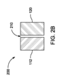
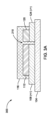
図2Aは、実施形態によれば、横で隣接する集電体および電極層を有する薄膜に基づくESD200の例の側面図を示している。図2Bは、図2Aに示された印刷されたエネルギー貯蔵装置の電極層の平面図を示している。図1に関して示されているESD100と同様に、ESD200は、基板104と、第1の集電体108と、第2の集電体124と、第1の電極層112と、第2の電極層120と、分離体116とを備える。図1に示されたESD100と異なり、ESD200では、第1の集電体108と第2の集電体124とは、基板104にわたって、または、基板104において、互いに対して横に隣接して形成されており、図1に関して先に記載されたESD100におけるような鉛直において分離される代わりに、横方向において隙間210によって分離されている。第1の電極層112は、第1の集電体108にわたって、または、第1の集電体108において形成されており、第2の電極層120は、第2の集電体124にわたって、または、第2の集電体124において形成されている。したがって、第1の電極層112と第2の電極層120とは、同じく互いに対して横に隣接して配置されており、鉛直において分離される代わりに、横方向において隙間210によって分離されている。分離体116は、第1の電極層112と第2の電極層120とを電気的に分離するために、第1の電極層112および第2の電極層120にわたって、または、第1の電極層112および第2の電極層120において形成されている。
FIG. 2A shows a side view of an example thin film-based
第1の電極層112は、第1の集電体108の設置面積内で横に形成されるように、第1の集電体108の横寸法とほぼ同じかそれより小さい横寸法を有する。同様に、第2の電極層120は、第2の集電体124の設置面積内で横に形成されるように、第2の集電体124の横寸法とほぼ同じかそれより小さい横寸法を有する。分離体116は、例えば第1の集電体108の第1の側面および第2の側面に接触するといった、それらの側面にわたって、または、それらの側面において形成され、第1の電極112を封入しており、また、例えば第2の集電体124の第1の側面および第2の側面に接触するといった、それらの側面にわたって、または、それらの側面において形成され、第2の電極層120を封入している。分離体116は、第1の電極層112と第2の電極層120との間に形成された隙間210を埋めており、それによって、横方向において互いを向いている第1の電極層112の側面と第2の電極層120の側面とを電気的に分離している。分離体116は、第1の集電体108と第2の集電体124との間に形成された隙間210の部分も埋めており、それによって、互いを向いている第1の集電体108の側面と第2の集電体124の側面とを電気的に分離している。
The
図2Aおよび図2Bをなおも参照すると、動作中、電圧が第1の集電体108と第2の集電体124との間に加えられるとき、イオンが分離体116を通じて第1の電極層112と第2の電極層120との間で交換され、それによってESD200を充電または放電させることができる。ESD100(図1)と異なり、第1の電極層112と第2の電極層120との横の配置のため、イオン交換の実質的または支配的な部分は横方向において起こることができる。イオン交換は、第1の電極層112の側面および上面と第2の電極層120の側面および上面との間で起こり得る。側面と上面との間でのイオン電流の相対的な量は、層の厚さ(および、側面同士の間の重なりの面積)と、上面の面積とに依存して変化し得る。側面同士の間の重なりの面積が比較的大きい場合、例えば、イオン交換の実質的または支配的な部分は、隙間210を挟んで互いを向く第1の電極層112の側面と第2の電極層120の側面との重なる部分の間で起こり得る。
Still referring to FIGS. 2A and 2B, in operation, when a voltage is applied between first
ESD200の1つまたは複数の層が印刷されるとき、ESD200を製作する方法は、共通の基板104にわたって、または、共通の基板104において、横で隣接し、電気的に分離された第1の集電体108および第2の集電体124を、例えば印刷するといった、堆積させることを含む。第1の集電層108および第2の集電層124は同時に印刷でき、同じ材料から形成できる。第1の集電体108および第2の集電体124を印刷した後、第1の電極層112および第2の電極層120はそれぞれ、それぞれの集電体108および124にわたって、または、それぞれの集電体108および124において、例えば印刷されるといった、堆積させられる。第1の電極112および第2の電極120を印刷した後、分離体116は、第1の電極層112および第2の電極層120にわたって、または、第1の電極層112および第2の電極層120において、例えば印刷されるといった、堆積させられる。第1の集電層108および第2の集電層124が同時に印刷されるとき、図示されているESD200は、第1の集電体108および第2の集電体124を同時に印刷することと、第1の電極層112を印刷することと、第2の電極層120を印刷することと、分離体116を印刷することとを含む4回の堆積ステップまたは印刷の刷りで製作できる。
When one or more layers of
したがって、図1に示されているような鉛直に積み重ねられた電極を有するESD100を製作する方法と比較して、横に配置された電極を有するESD200は、図1に示されているESD100を製作するときに使用される5回の工程ステップまたは印刷の刷りと比較して、例えばわずか4回の工程ステップまたは印刷の刷りでといったより少ない工程ステップで、例えば印刷できるといった有利に製作することができる。
Therefore, compared to the method of fabricating
集電体の厚さは用途に応じて変わってもよい。例えば、一部の実施では、より小さい電気抵抗のために、より厚い第1の集電体108および第2の集電体124を有することが望ましい可能性がある。一部の実施では、より大きい容量を提供するために、より厚い第1の電極層112および第2の電極層120を有することが望ましい可能性がある。ESD200では、より厚い電極層112、120は、より大きい電流能力を提供することもできる。
The thickness of the current collector may vary depending on the application. For example, in some implementations it may be desirable to have thicker first
本明細書に記載されている様々な実施形態において、個々の層またはESD全体の各々は、1~10ミクロン、10~50ミクロン、50~100ミクロン、100~200ミクロン、200~300ミクロン、300~400ミクロン、400~500ミクロン、500~600ミクロン、600~700ミクロン、700~800ミクロン、800~900ミクロン、900~1000ミクロン、1000~1200ミクロン、1200~1400ミクロン、1400~1600ミクロン、1600~1800ミクロン、1800~2000ミクロンの範囲での厚さ、または、これらの値のいずれかによって定められる範囲での厚さを有し得る。 In various embodiments described herein, each individual layer or overall ESD is 1-10 microns, 10-50 microns, 50-100 microns, 100-200 microns, 200-300 microns, 300 microns, ~400 microns, 400-500 microns, 500-600 microns, 600-700 microns, 700-800 microns, 800-900 microns, 900-1000 microns, 1000-1200 microns, 1200-1400 microns, 1400-1600 microns, 1600 It may have a thickness in the range of -1800 microns, 1800-2000 microns, or a range defined by any of these values.
鉛直の電極配置(例えば、図1におけるESD100)および横の電極の配置(例えば、図2A~図2BにおけるESD200)が同じ利点または異なる利点を提供することは、理解されるものである。先に詳述されているように、ESD200(図2A~図2B)は、比較的より少ない工程ステップで製作でき、ESD100(図1)と比較してより薄くできる。一方で、ESD100(図1)は、同じ容量および電流について、ESD200(図2A~図2B)と比較してより小さい横の設置面積を有することができる。ESD100(図1)と比較して、鉛直に積み重ねられた層の全体の数がより少ないことで、境界面における割れおよび/または剥離の危険性を低下させることができるため、ESD200は、より薄い装置全体の厚さ、および/または、同様の全体の厚さについては比較的より厚い個々の層を有するように、有利に許容され得る。一方で、ESD200(図2A~図2B)は、電極同士の重なりが比較的より小さいため、ESD100(図1)と比較してより小さい電流能力を有し得る。以下において、図1および図2A/図2Bに関連して示された2つの異なる種類のESDによって提供される利点を最適化することを目指している様々な他の実施形態およびそれらの構成要素が記載されている。ESD100(図1)と比較して、ESD200(図2)の第2の集電体124は、基板104から延びる比較的長い鉛直部分を有しておらず、これはESD200の全体の抵抗を低下させることができる。また、ESD100の鉛直方向高さが比較的高い場合、機械的な支持層(図1では示されていない)がESD100の第2の集電体124の鉛直部分を支持するために設けられてもよく、これはESD200では有利には必要とされない。
It is understood that vertical electrode placement (eg,
薄膜に基づくエネルギー貯蔵装置を製作するための印刷方法
本明細書で開示されているESDの1つまたは複数の層は、構成要素の材料を含むインクから印刷できる。1つもしくは複数の層またはESD装置全体は、適切な印刷技術を用いて印刷され得る。1つもしくは複数の層を印刷するために使用できる例の印刷工程には、数ある適切な印刷技術の中でも、例えばスクリーン印刷、インクジェット印刷、電気光学印刷、電子インク印刷、フォトレジストおよび他のレジスト印刷、熱転写印刷、レーザージェット印刷、磁気印刷、パッド印刷、フレキソ印刷、ハイブリッドオフセット石版印刷、グラビア印刷、他の凹版印刷、およびダイスロット蒸着といった、コーティング、回転、噴霧、積層、スピンコーティング、ラミネーション、および/または貼り付けの工程がある。
Printing Methods for Fabricating Thin Film-Based Energy Storage Devices One or more layers of the ESDs disclosed herein can be printed from inks containing constituent materials. One or more layers or the entire ESD device can be printed using a suitable printing technique. Example printing processes that can be used to print one or more layers include, for example, screen printing, inkjet printing, electro-optic printing, electronic ink printing, photoresists and other resists, among other suitable printing techniques. Coating, spinning, spraying, laminating, spin coating, lamination, such as printing, thermal transfer printing, laser jet printing, magnetic printing, pad printing, flexographic printing, hybrid offset lithographic printing, gravure printing, other intaglio printing, and die slot deposition. and/or there is a step of pasting.
本明細書で開示されているESDの1つまたは複数の層を印刷するためのインクは、ESDの電気化学反応と関連付けられる様々な活物質を含む様々なインク構成要素を適切な溶媒および/または結合剤と組み合わせることと、いくつか名前を挙げれば、攪拌棒を使用して混合することなどの適切な技術を用いて混合すること、マグネチックスターラで混合すること、ボルテックスすること(渦流機械を使用する)、振ること(シェーカを使用する)、3つのロールミル、ボールミルを回転によって自転公転攪拌すること、超音波処理、ならびに、乳鉢および乳棒を用いて混合することとによって準備され得る。 Inks for printing one or more layers of the ESD disclosed herein contain various ink components, including various active materials associated with the electrochemical reactions of the ESD, in suitable solvents and/or Combining with a binder and mixing using any suitable technique such as mixing using a stir bar, mixing with a magnetic stirrer, vortexing (using a vortex machine, to name a few). (using a shaker), shaking (using a shaker), 3 roll mill, orbital stirring by rotating a ball mill, sonication, and mixing with a mortar and pestle.
インクを用いて1つまたは複数の層を印刷した後、1つまたは複数の層は、数ある技術の中でも、短波赤外線(IR)放射、中波IR放射、高温空気対流オーブン、電子ビーム硬化、紫外線(UV)硬化、および近赤外線放射を含む乾燥/硬化の工程を含め、1つまたは複数の印刷後工程を用いて処理され得る。 After printing one or more layers with an ink, one or more layers are subjected to, among other techniques, short wave infrared (IR) radiation, medium wave IR radiation, hot air convection oven, electron beam curing, It can be processed using one or more post-printing steps, including ultraviolet (UV) curing, and drying/curing steps involving near-infrared radiation.
薄膜に基づくエネルギー貯蔵装置の層の組成および材料
以下において、実施形態による薄膜に基づくESDの様々な層の組成、材料、および構造が記載されている。
Compositions and Materials of Layers of Thin Film-Based Energy Storage Devices In the following, compositions, materials, and structures of various layers of thin film-based ESDs according to embodiments are described.
薄膜に基づくESDは、基板104において、例えば印刷された、形成された様々な層を備える。基板は、数ある特質の中でも、柔軟性もしくは剛性であること、熱的に伝導性もしくは絶縁性であること、光学的に透明もしくは不透明であること、または有機もしくは無機であることなどの特質を有し得る適切な材料から形成できる。第1の集電体108および第2の集電体124が基板に直接的に形成されるとき、第1の集電体108と第2の集電体124とが電気的に短絡されないように、または、それらの間の漏れ電流が十分に小さくなるように、基板104は十分に電気的に絶縁の材料から形成される。本明細書において記載されているように、電気的に絶縁の材料は、熱的に、電気的に、または光学的に通常の動作条件の下で発生させられ得る電子および孔などの電子キャリアを無視できる程度に有する材料を言っており、シリコンなどの半導体材料を除外する。しかしながら、基板104は、例えば、第1の集電体108と第2の集電体124とが電気的に短絡されないように、第1の集電体108および第2の集電体124を形成する前に半導体または導電性の基板に絶縁層またはコーティングを形成することで、表面領域が十分に電気的に絶縁とされている導電性または半導体の材料を含んでもよい。
A thin film-based ESD comprises various layers formed, for example printed, on the
基板104の一部として含まれ得る適切な等級の材料には、限定されることはないが、高分子材料、織物に基づく材料、装置、金属材料、半導体材料、またはセルロースに基づく材料がある。基板104の特定の例には、例えば、プラスチック(例えば、ポリエステル、ポリイミド、ポリカーボネート)、誘電体(例えば、金属酸化物、金属窒化物、金属炭化物)、ポリエステル膜(例えば、マイラー)、ポリカーボネート膜、半導体(例えば、シリコン)、導体(例えば、アルミ箔、銅箔、ステンレス鋼箔)、炭素発泡体、紙(例えば、黒鉛紙、グラフェン紙、厚紙、プラスチックコート紙などのコート紙、および/または繊維紙)、またはそれらの組み合わせなどがある。
Suitable grades of materials that may be included as part of
様々な実施形態によれば、第1の電極層112は陽極または陰極の一方とすることができ、第2の電極層120は陽極または陰極の他方を備え得る。エネルギー貯蔵装置の陽極は、銀含有物質またはマンガン含有物質をなどの陽極電極活物質を備え得る。例えば、陽極は、第1の電極層または第2の電極層の一方は、銀(I)酸化物(Ag2O)、銀(I, III)酸化物(AgO)、銀(I)酸化物(Ag2O)およびマンガン(IV)酸化物(MnO2)を含む混合物、マンガン(II, III)酸化物(Mn3O4)、マンガン(II)酸化物(MnO)、マンガン(III)酸化物(Mn2O3)、オキシ水酸化マンガン(MnOOH)、銀(I)酸化物(Ag2O)およびオキシ水酸化ニッケル(NiOOH)を含む混合物、銀ニッケル酸化物(AgNiO2)、それらの組み合わせなどを含み得る。エネルギー貯蔵装置の陰極は、亜鉛、カドミウム、鉄、ニッケル、アルミニウム、金属水和物、水素、それらの組み合わせなどの陰極電極活物質を含み得る。一部の実施形態では、陰極は亜鉛粉末を含み得る。
According to various embodiments, the
一部の実施形態では、本明細書に開示されている薄膜に基づくESDは、例えば、第1の電極層112、第2の電極層120、もしくは分離体116のうちの1つまたは複数の一部として、非水電解質を含んでもよい。非水電解質は、数ある有機電解質の中でも、アセトニトリル、プロピレンカーボネート、エチレンカーボネート、ジエチルカーボネート、ジメチルカーボネート、酢酸エチル、1,1,1,3,3,3-ヘキサフルオロプロパン-2-オール、アジポニトリル、1,3-プロピレンサルファイト、ブチレンカーボネート、γ-ブチロラクトン、γ-バレロラクトン、プロピオニトリル、グルタロニトリル、アジポニトリル、メトキシアセトニトリル、3-メトキシプロピオニトリル、N,N-ジメチルホルムアミド、N,N-ジメチルアセトアミド、N-メチルピロリジノン、N-メチルオキサゾリジノン、N,N"-ジメチルイミダゾリノン、ニトロメタン、ニトロエタン、スルホネート、3-メチルスルホネート、ジメチルスルホキシド、トリメチルホスフェート、またはそれらの組み合わせに基づく有機電解質をさらに含み得る。
In some embodiments, the thin film-based ESD disclosed herein includes one or more of the
一部の実施形態では、電解質はイオン液体を含み得る。本明細書において記載されているように、イオン液体は、本質的にイオンから成る有機溶融塩であり、100℃未満の温度において液体である。イオン液体はカチオンとアニオンとを有する。実施形態によるイオン液体は、後にあるカチオンの列記とアニオンの列記とからの任意の組み合わせを含み得る。 In some embodiments, the electrolyte can include an ionic liquid. As described herein, ionic liquids are organic molten salts that consist essentially of ions and are liquid at temperatures below 100°C. Ionic liquids have cations and anions. Ionic liquids according to embodiments may comprise any combination from the lists of cations and anions that follow.
イオン液体のカチオンは、ブチルトリメチルアンモニウム、1-エチル-3-メチルイミダゾリウム、1-ブチル-3-メチルイミダゾリウム、1-メチル-3-プロピルイミダゾリウム、1-ヘキシル-3-メチルイミダゾリウム、コリン、エチルアンモニウム、トリブチルメチルホスホニウム、トリブチル(テトラデシル)ホスホニウム、トリヘキシル(テトラデシル)ホスホニウム、1-エチル-2,3-メチルイミダゾリウム、1-ブチル-1-メチルピペリジニウム、ジエチルメチルスルホニウム、1-メチル-3-プロピルイミダゾリウム、1-エチル-3-メチルイミダゾリウム、1-メチル-1-プロピルピペリジニウム、1-ブチル-2-メチルピリジニウム、1-ブチル-4-メチルピリジニウム、1-ブチル-1-メチルピロリジニウム、ジエチルメチルスルホニウム、またはそれらの組み合わせのうちの1つまたは複数を含み得る。 The ionic liquid cations are butyltrimethylammonium, 1-ethyl-3-methylimidazolium, 1-butyl-3-methylimidazolium, 1-methyl-3-propylimidazolium, 1-hexyl-3-methylimidazolium, Choline, ethylammonium, tributylmethylphosphonium, tributyl(tetradecyl)phosphonium, trihexyl(tetradecyl)phosphonium, 1-ethyl-2,3-methylimidazolium, 1-butyl-1-methylpiperidinium, diethylmethylsulfonium, 1- Methyl-3-propylimidazolium, 1-ethyl-3-methylimidazolium, 1-methyl-1-propylpiperidinium, 1-butyl-2-methylpyridinium, 1-butyl-4-methylpyridinium, 1-butyl -1-methylpyrrolidinium, diethylmethylsulfonium, or combinations thereof.
イオン液体のアニオンは、トリス(ペンタフルオロエチル)トリフルオロホスフェート、トリフルオロメタンスルホネート、ヘキサフルオロホスフェート、テトラフルオロボレート、硫酸エチル、リン酸ジメチル、トリフルオロメタンスルホネート、メタンスルホネート、トリフレート、トリシアノメタニド、ジブチルホスフェート、ビス(トリフルオロメチルスルホニル)イミド、ビス-2,4,4-(トリメチルペンチル)ホスフィネート、ヨウ化物、塩化物、臭化物、硝酸塩、またはそれらの組み合わせのうちの1つまたは複数を含み得る。 The anions of the ionic liquids are tris(pentafluoroethyl)trifluorophosphate, trifluoromethanesulfonate, hexafluorophosphate, tetrafluoroborate, ethyl sulfate, dimethyl phosphate, trifluoromethanesulfonate, methanesulfonate, triflate, tricyanometanide, may include one or more of dibutyl phosphate, bis(trifluoromethylsulfonyl)imide, bis-2,4,4-(trimethylpentyl)phosphinate, iodide, chloride, bromide, nitrate, or combinations thereof .
一部の実施形態では、電解質は、有機、酸、塩基、または無機に基づかれ得る電解質塩をさらに含んでもよい。例えば、電解質の一部として含まれ得る有機塩は、テトラエチルアンモニウムテトラフルオロボレート、テトラエチルアンモニウムジフルオロ(オキサレート)ボレート、メチルアンモニウムテトラフルオロボレート、トリエチルメチルアンモニウムテトラフルオロボレート、テトラフルオロホウ酸ジメチルジエチルアンモニウム、トリエチルメチルアンモニウムテトラフルオロボレート、テトラプロピルアンモニウムテトラフルオロボレート、メチルトリブチルアンモニウムテトラフルオロボレート、テトラブチルアンモニウムテトラフルオロボレート、テトラヘキシルアンモニウムテトラフルオロボレート、テトラメチルアンモニウムテトラフルオロボレート、テトラエチルホスホニウムテトラフルオロボレート、テトラプロピルホスホニウムテトラフルオロボレート、テトラブチルホスホニウム、テトラフルオロボレート、またはそれらの組み合わせのうちの1つまたは複数を含む。 In some embodiments, the electrolyte may further comprise electrolyte salts, which may be organic, acid, basic, or inorganic. For example, organic salts that can be included as part of the electrolyte are tetraethylammonium tetrafluoroborate, tetraethylammonium difluoro(oxalate)borate, methylammonium tetrafluoroborate, triethylmethylammonium tetrafluoroborate, dimethyldiethylammonium tetrafluoroborate, triethyl methylammonium tetrafluoroborate, tetrapropylammonium tetrafluoroborate, methyltributylammonium tetrafluoroborate, tetrabutylammonium tetrafluoroborate, tetrahexylammonium tetrafluoroborate, tetramethylammonium tetrafluoroborate, tetraethylphosphonium tetrafluoroborate, tetrapropylphosphonium including one or more of tetrafluoroborate, tetrabutylphosphonium, tetrafluoroborate, or combinations thereof.
電解質の一部として含まれ得る酸に基づく電解質には、H2SO4、HCl、HNO3、HClO4、それらの組み合わせなどの1つまたは複数を含む。 Acid-based electrolytes that may be included as part of the electrolyte include one or more of H2SO4 , HCl, HNO3 , HClO4 , combinations thereof , and the like.
電解質の一部として含まれ得る塩基に基づく電解質には、KOH、NaOH、LiOH、NH4OH、それらの組み合わせなどの1つまたは複数を含む。 Base-based electrolytes that may be included as part of the electrolyte include one or more of KOH, NaOH, LiOH, NH4OH , combinations thereof, and the like.
電解質の一部として含まれ得る無機に基づく塩には、LiCl、Li2SO4、LiClO4、NaCl、Na2SO4、NaNO3、KCl、K2SO4、KNO3、Ca(NO3)2、MgSO4、ZnCl2、Zn(BF4)2、ZnNO3、それらの組み合わせなどの1つまたは複数を含む。 Inorganic based salts that can be included as part of the electrolyte include LiCl, Li2SO4 , LiClO4 , NaCl, Na2SO4 , NaNO3 , KCl, K2SO4 , KNO3 , Ca( NO3 ) 2 , MgSO4 , ZnCl2 , Zn( BF4 ) 2 , ZnNO3 , combinations thereof, and the like.
実施形態は、有機の電解質またはイオン液体に限定されない。他の実施形態では、実施形態によるESDは、水に基づく水性電解質を含む。 Embodiments are not limited to organic electrolytes or ionic liquids. In other embodiments, an ESD according to embodiments comprises a water-based aqueous electrolyte.
一部の実施形態では、低粘度添加物は電解質に加えられてもよい。電解質の一部として含まれ得る低粘度添加物には、水、メタノールなどのアルコール、エタノール、N-プロパノール(1-プロパノール、2-プロパノール(イソプロパノールまたはIPA)、1-メトキシ-2-プロパノールを含む)、ブタノール(1-ブタノール、2-ブタノール(イソブタノール)を含む)、ペンタノール(1-ペンタノール、2-ペンタノール、3-ペンタノールを含む)、ヘキサノール(1-ヘキサノール、2-ヘキサノール、3-ヘキサノールを含む)、オクタノール、N-オクタノール(1-オクタノール、2-オクタノール、3-オクタノール)、テトラヒドロフルフリルアルコール(THFA)、シクロヘキサノール、シクロペンタノール、テルピネオール、ブチルラクトンなどのラクトン、メチルエチルエーテル、ジエチルエーテル、エチルプロピルエーテル、およびポリエーテルなどのエーテル、シクロヘキサノン、シクロペンタノン、シクロヘプタノン、シクロオクタノン、アセトン、ベンゾフェノン、アセチルアセトン、アセトフェノン、シクロプロパノン、イソホロン、メチルエチルケトンなどのジケトンおよび環状ケトンを含むケトン、酢酸エチルなどのエステル、アジピン酸ジメチル、プロピレングリコールモノメチルエーテルアセテート、グルタル酸ジメチル、コハク酸ジメチル、酢酸グリセリン、カルボン酸塩、炭酸プロピレンなどの炭酸塩、ポリオール(または液体ポリオール)、グリセロール、および、グリセリン、ジオール、トリオール、テトラオール、ペンタオール、エチレングリコール、ジエチレングリコール、ポリエチレングリコール、プロピレングリコール、ジプロピレングリコール、グリコールエーテル、グリコールエーテルアセテート、1,4-ブタンジオール、1,2-ブタンジオール、2,3-ブタンジオール、1,3-プロパンジオール、1,4-ブタンジオール、1,5-ペンタンジオール、1,8-オクタンジオール、1,2-プロパンジオール、1,3-ブタンジオール、1,2-ペンタンジオール、エトヘキサジオール、p-メンタン-3,8-ジオール、2-メチル-2,4-ペンタンジオールなどの他の高分子ポリオールまたはグリコール、テトラメチル尿素、n-メチルピロリドン、アセトニトリル、テトラヒドロフラン(THF)、ジメチルホルムア
ミド(DMF)、N-メチルホルムアミド(NMF)、ジメチルスルホキシド(DMSO)、塩化チオニル;塩化スルフリル、またはそれらの組み合わせのうちの1つまたは複数を含む。数ある利点の中でも、低粘度添加物は、印刷されるときに電解質の拡散速度を向上させることができる。開示されている添加物が、本明細書に記載されている様々な印刷の電気化学反応物質の組み合わせにおいて実質的に電気化学的に安定であり得ることは、理解されるものである。
In some embodiments, low viscosity additives may be added to the electrolyte. Low viscosity additives that can be included as part of the electrolyte include water, alcohols such as methanol, ethanol, N-propanol (1-propanol, 2-propanol (isopropanol or IPA), 1-methoxy-2-propanol ), butanol (including 1-butanol, 2-butanol (isobutanol)), pentanol (including 1-pentanol, 2-pentanol, 3-pentanol), hexanol (1-hexanol, 2-hexanol, 3-hexanol), octanol, N-octanol (1-octanol, 2-octanol, 3-octanol), tetrahydrofurfuryl alcohol (THFA), cyclohexanol, cyclopentanol, terpineol, lactones such as butyl lactone, methyl Ethers such as ethyl ether, diethyl ether, ethyl propyl ether, and polyethers, diketones such as cyclohexanone, cyclopentanone, cycloheptanone, cyclooctanone, acetone, benzophenone, acetylacetone, acetophenone, cyclopropanone, isophorone, methyl ethyl ketone, and Ketones including cyclic ketones, esters such as ethyl acetate, dimethyl adipate, propylene glycol monomethyl ether acetate, dimethyl glutarate, dimethyl succinate, glycerin acetate, carboxylates, carbonates such as propylene carbonate, polyols (or liquid polyols) , glycerol and glycerin, diol, triol, tetraol, pentaol, ethylene glycol, diethylene glycol, polyethylene glycol, propylene glycol, dipropylene glycol, glycol ether, glycol ether acetate, 1,4-butanediol, 1,2- Butanediol, 2,3-butanediol, 1,3-propanediol, 1,4-butanediol, 1,5-pentanediol, 1,8-octanediol, 1,2-propanediol, 1,3-butane Other polymeric polyols or glycols such as diols, 1,2-pentanediol, ethhexadiol, p-menthane-3,8-diol, 2-methyl-2,4-pentanediol, tetramethylurea, n-methyl pyrrolidone, acetonitrile, tetrahydrofuran (THF), dimethylformamide (DMF), N-methylformamide (NMF), dimethylsulfoxide (DMSO), thionyl chloride; sulfuryl chloride, or combinations thereof. Among other benefits, low viscosity additives can improve the electrolyte diffusion rate when printed. It is understood that the disclosed additives can be substantially electrochemically stable in the various printing electrochemical reactant combinations described herein.
一部の実施形態では、電解質は界面活性剤を含む。例えば、界面活性剤は非イオンであり得る。電解質の一部として含まれ得る非イオンの界面活性剤には、セチルアルコール、ステアリルアルコール、セトステアリルアルコール、オレイルアルコール、ポリオキシエチレングリコールアルキルエーテル、オクタエチレングリコールモノドデシルエーテル、グルコシドアルキルエーテル、デシルグルコシド、ポリオキシエチレングリコールオクチルフェノールエーテル、Triton(登録商標) X-100(Sigma-Aldrich(登録商標)によって販売されている)、ノノキシノール-9、ラウリン酸グリセリル、ポリソルベート、ポロキサマ、またはそれらの組み合わせのうちの1つまたは複数を含む。数ある利点の中でも、界面活性剤は、印刷されるときに電解質の拡散速度を向上させることができる。開示されている添加物が、本明細書に記載されている様々な印刷の電気化学反応物質の組み合わせにおいて実質的に電気化学的に安定であり得ることは、理解されるものである。 In some embodiments the electrolyte comprises a surfactant. For example, surfactants can be non-ionic. Nonionic surfactants that may be included as part of the electrolyte include cetyl alcohol, stearyl alcohol, cetostearyl alcohol, oleyl alcohol, polyoxyethylene glycol alkyl ethers, octaethylene glycol monododecyl ether, glucoside alkyl ethers, decyl glucoside. , polyoxyethylene glycol octylphenol ether, Triton® X-100 (sold by Sigma-Aldrich®), nonoxynol-9, glyceryl laurate, polysorbates, poloxamers, or combinations thereof. Contains one or more. Among other benefits, surfactants can improve the diffusion rate of the electrolyte when printed. It is understood that the disclosed additives can be substantially electrochemically stable in the various printing electrochemical reactant combinations described herein.
一部の実施形態では、分離体は充填剤を含み得る。充填剤は、数ある充填剤の中でも、珪藻フラスチュール、ゼオライト、セルロース繊維、ガラス繊維、アルミナ、シリカゲル、モレキュラーシーブカーボン、天然粘土ベースの固体、高分子吸収剤、もしくはそれらの組み合わせのうちの1つまたは複数を含み得る。 In some embodiments, the separator may contain fillers. The filler is one of diatom frustules, zeolites, cellulose fibers, glass fibers, alumina, silica gel, molecular sieve carbon, natural clay-based solids, polymeric absorbents, or combinations thereof, among other fillers. may include one or more.
一部の実施形態では、分離体は高分子バインダを含み得る。高分子バインダは、ポリビニルピロリドン(PVP)、ポリビニルアルコール(PVA)、ポリフッ化ビニリデン、フッ化ポリビニリデン-トリフルオロエチレン、ポリテトラフルオロエチレン、ポリジメチルシロキサン、ポリエチレン、ポリプロピレン、ポリエチレンオキシド、ポリプロピレンオキシド、ポリエチレングリコールヘキサフルオロプロピレン、ポリエチレンテレフタレートポリアクリロニトリル、ポリビニルブチラール、ポリビニルカプロラクタム、ポリ塩化ビニルなどのポリマ(または、同等に、高分子前駆体または重合性前駆体)、ポリイミドポリマおよびコポリマ(脂肪族、芳香族、および半芳香族ポリイミドを含む)、ポリアミド、ポリアクリルアミド、アクリレート、(メタ)アクリレートポリマ、および、ポリメチルメタクリレート、ポリアクリロニトリル、アクリロニトリルブタジエンスチレン、アリルメタクリレート、ポリスチレン、ポリブタジエン、ポリブチレンテレフタレート、ポリカーボネート、ポリクロロプレン、ポリエーテルスルホン、ナイロン、スチレン-アクリロニトリル樹脂などのコポリマ、ポリエチレングリコール、ヘクトライト粘土、ガラマイト粘土、有機変性粘土などの粘土、糖類および、グアーガム、キサンタンガム、デンプン、ブチルゴム、アガロース、ペクチンなどの多糖類、セルロースおよび、ヒドロキシルセルロース、メチルセルロース、エチルセルロース、プロピルメチルセルロース、メトキシセルロース、メトキシメチルセルロース、メトキシプロピルメチルセルロース、ヒドロキシプロピルメチルセルロース、カルボキシメチルセルロース、ヒドロキシエチルセルロース、エチルヒドロキシルエチルセルロース、セルロースエーテル、セルロースエチルエーテル、キトサンなどの修飾セルロース、もしくはそれらの組み合わせのうちの1つまたは複数を含み得る。 In some embodiments, the separator may include a polymeric binder. Polymeric binders include polyvinylpyrrolidone (PVP), polyvinyl alcohol (PVA), polyvinylidene fluoride, polyvinylidene fluoride-trifluoroethylene, polytetrafluoroethylene, polydimethylsiloxane, polyethylene, polypropylene, polyethylene oxide, polypropylene oxide, polyethylene Polymers (or, equivalently, polymeric or polymeric precursors), polyimide polymers and copolymers (aliphatic, aromatic, and semi-aromatic polyimides), polyamides, polyacrylamides, acrylate, (meth)acrylate polymers and polymethyl methacrylate, polyacrylonitrile, acrylonitrile butadiene styrene, allyl methacrylate, polystyrene, polybutadiene, polybutylene terephthalate, polycarbonate, polychloroprene , polyether sulfone, nylon, copolymers such as styrene-acrylonitrile resin, clays such as polyethylene glycol, hectorite clay, garamite clay, organic modified clay, sugars and polysaccharides such as guar gum, xanthan gum, starch, butyl rubber, agarose, pectin , cellulose and modified cellulose such as hydroxyl cellulose, methyl cellulose, ethyl cellulose, propyl methyl cellulose, methoxy cellulose, methoxymethyl cellulose, methoxypropyl methyl cellulose, hydroxypropyl methyl cellulose, carboxymethyl cellulose, hydroxyethyl cellulose, ethyl hydroxyl ethyl cellulose, cellulose ether, cellulose ethyl ether, chitosan. , or combinations thereof.
明確性のために図示されていないが、外界からのESDへの機械的、電気的、および化学的な防御を提供するために、本明細書に開示されている様々なESDの上に防御膜が形成されてもよいことは、理解されるものである。防御膜は、例えばラミネートまたは印刷され得る。ESDの包装は簡潔性のために詳述されないが、包装が薄膜に基づくESDの一体の一部を形成し、延いては完成した製品の一部を形成することは、理解されるものである。 Although not shown for clarity, protective membranes were placed over the various ESDs disclosed herein to provide mechanical, electrical, and chemical protection against ESD from the outside world. may be formed. The protective membrane can be laminated or printed, for example. The packaging of the ESD is not detailed for the sake of brevity, but it is understood that the packaging forms an integral part of the film-based ESD and thus forms part of the finished product. .
薄膜に基づくエネルギー貯蔵装置の構成
図1および図2A/図2Bに関連して前述したように、薄膜に基づくESDには、2つの大まかな種類、つまり、図1に関連して前述した例のESD100など、鉛直に積み重ねられた電極層および集電体を有する薄膜に基づくESDと、図2A/図2Bに関連して前述した例のESD200など、横で隣接する集電体および電極を有する薄膜に基づくESDとがある。前述したように、2つの大まかな種類の薄膜に基づくESDの各々は、2種類の薄膜に基づくESDの他方に対して特定の利点を有し得る。例えば、横に配置された集電体と電極とを有するESDは、より少ない数の刷りまたは工程ステップで印刷することができ、電極および/または集電体のより大きい層の厚さを受け入れることができるため有利にできる。一方、鉛直に配置された電極層と集電体とを有するESDは、相対する電極層同士の間の重なりのより大きい面積と、イオンについてのそれら電極層同士の間のより短い進行距離とによるより大きな電流能力のため有利にできる。以下において、2つの大まかな種類の薄膜に基づくESDの様々な実施形態が開示されており、それらは、その構成要素の層の物理的な配置に一部基づいて、これらの利点および他の利点を提供できる。
Configurations of Thin-Film-Based Energy Storage Devices As described above in connection with FIGS. 1 and 2A/2B, there are two broad classes of thin-film-based ESDs: ESD based on thin films with vertically stacked electrode layers and current collectors, such as ESD100, and thin films with laterally adjacent current collectors and electrodes, such as ESD200 in the example described above in connection with FIGS. 2A/2B Based on ESD. As mentioned above, each of the two general types of thin film-based ESD can have certain advantages over the other of the two types of thin film-based ESD. For example, ESDs with laterally arranged current collectors and electrodes can be printed in fewer passes or process steps, accommodating larger layer thicknesses of electrodes and/or current collectors. can be advantageous. On the other hand, ESD with vertically arranged electrode layers and current collectors, due to the larger area of overlap between the opposing electrode layers and the shorter travel distance between the electrode layers for ions, Advantageously due to the greater current capability. In the following, various embodiments of thin-film-based ESDs of two broad types are disclosed, and these and other advantages are based in part on the physical arrangement of their constituent layers. can provide
様々な薄膜に基づくESDでは、電極活物質の相対的な体積および/または質量が、いくつかの理由のため、反対の極性の電極活物質同士の間で異なるように調節されてもよい。例えば、電気化学反応を伴う電池などの薄膜に基づくESDでは、例えば陽極活物質および陰極活物質といった第1の電極活物質および第2の電極活物質の相対的な量は、ESDの根底にある電気化学反応に基づいて異なるように調節され得る。例えば、電気化学反応に関与する第1の電極活物質の量と第2の電極活物質の量との間の比はモル基準で約1:1である薄膜に基づくESDでは、第1の電極活物質および第2の電極活物質は、モル基準において約1:1の比でそれぞれの電極層に配置され得る。しかしながら、電気化学反応に関与する第1の電極活物質の量と第2の電極活物質の量との比が、モル基準において1:1より大きい/小さい、または、第1の電極活物質と第2の電極活物質との間の様々な他の構造および材料の違いのため1:1より大きい/小さい薄膜に基づくESDでは、第1の電極活物質および第2の電極活物質の相対的な体積ならびに/または質量は、相当に異なるように調節され得る。様々な実施形態において、電極活物質の体積および/または質量は、電極の面積および/または厚さを調節することによって調節できる。図3Aおよび図3Bは、第1の電極層112および第2の電極層120の活物質の体積および/または質量が、第1の電極層112および第2の電極層120の少なくとも表面積を調節することによって調節できる薄膜に基づくESD300を示している。
In various thin film-based ESDs, the relative volume and/or mass of electrode active materials may be adjusted differently between electrode active materials of opposite polarity for several reasons. For example, in thin film-based ESD, such as batteries involving electrochemical reactions, the relative amounts of first electrode active material and second electrode active material, such as positive electrode active material and negative electrode active material, underlie the ESD. It can be adjusted differently based on the electrochemical reaction. For example, in a thin film-based ESD in which the ratio between the amount of the first electrode active material and the amount of the second electrode active material participating in the electrochemical reaction is about 1:1 on a molar basis, the first electrode The active material and the second electrode active material may be disposed on each electrode layer in a ratio of about 1:1 on a molar basis. However, the ratio of the amount of the first electrode active material to the amount of the second electrode active material participating in the electrochemical reaction is greater/less than 1:1 on a molar basis, or Due to various other structural and material differences between the second electrode active material, in thin film-based ESD greater than/less than 1:1, the relative The volume and/or mass can be adjusted quite differently. In various embodiments, the volume and/or mass of electrode active material can be adjusted by adjusting the area and/or thickness of the electrode. 3A and 3B show that the volume and/or mass of the active material of the
図3Aは、第1の電極層と第2の電極層との間の表面積の比が活物質のモル比に従って調節されている、非対称に横で隣接する集電体および電極層を有する薄膜に基づくエネルギー貯蔵装置300の側面図を示している。図3Bは、図3Aに示された薄膜に基づくエネルギー貯蔵装置の電極層の平面図を示している。図2Aおよび図2Bに関連して図示されたESD200と同様に、ESD300は、第1の集電体108および第2の集電体124が基板104において互いに横で隣接して形成されており、横方向において隙間210によって分離されていることを含む。ESD300は、第1の集電体108および第2の集電体124にわたって、または、第1の集電体108および第2の集電体124においてそれぞれ形成された第1の電極層112および第2の電極層120を追加的に含み、同じく、互いに対して横で隣接して形成されており、横方向において隙間210によって分離されている。分離体116は、第1の電極層112および第2の電極層120にわたって、または、第1の電極層112および第2の電極層120において形成されている。しかしながら、図2Aおよび図2BのESD200と異なり、第1の電極層112および第2の電極層120の横の設置面積または表面積は異なり、非対称である。具体的には、第1の電極層112の表面積と第2の電極層120の表面積との割合は、前述したように、根底にある電気化学反応に従って、例えば陽極の活物質および陰極の活物質といった、第1の電極の電極活物質と第2の電極の電極活物質との化学量論比に従って調節される。例えば、根底にある電気化学反応に伴う、例えば陽極の活物質および陰極の活物質といった、第1の電極活物質の量と第2の電極活物質の量との比が、モル基準において1:1であるとき、第1の電極活物質を含む第1の電極層112の第1の体積V1と第2の電極活物質を含む第2の電極層120の第2の体積V2との間の比V1/V2は、第2の電極活物質の第2のモル質量m2に対する第1の電極活物質の第1のモル質量m1の比m1/m2に比例してもよく、第1の電極活物質の第1の密度ρ1に対する第2の電極活物質の第2の密度ρ2の比ρ2/ρ1に比例してもよい。比V1/V2を調節するために、一部の実施では、第1の電極層112および第2の電極層120の表面積は調節される一方で、それらの厚さを比較的一定に保つ。これらの実施では、第1の電極層112および第2の電極層120がおおよそ同じ厚さを有する矩形の平板として近似できる形状において、電気化学反応に伴う、例えば陽極の活物質および陰極の活物質といった、第1の電極活物質と第2の電極活物質との比が、モル比に基づいて1:1であるとき、第1の電極層112の第1の表面積A1と第2の電極層120の第2の表面積A2との間の比A1/A2は、比m1/m2および比ρ2/ρ1に比例してもよい。
FIG. 3A shows a thin film having asymmetrically laterally adjacent current collector and electrode layers, where the ratio of surface areas between the first electrode layer and the second electrode layer is adjusted according to the molar ratio of the active materials. 3 shows a side view of an
なおも図3A/図3Bを参照すると、第1の電極層は第1の電極活物質を備え、第2の電極層は第2の電極活物質を備え、第1の電極活物質と第2の電極活物質との間のモル比が、0.1から0.4の間、0.4から0.7の間、0.7から1.0まで、1.0から1.3まで、1.3から1.6まで、1.6から1.9まで、1.9から2.2まで、2.2から2.5まで、2.5から2.8まで、2.8から3.1まで、3.1から3.4まで、3.4から3.7まで、3.7から4.0まで、4.0から4.3まで、または、これらの値のいずれかによって定められる範囲にあり、モル比は、ESDの根底にある電気化学反応に対応できる。例えば、図示の例として、ESDは、第1の電極活物質が亜鉛を備え、第2の電極活物質がMnO2を備えるアルカリ電池を備え、第1の電極活物質と第2の電極活物質との間のモル比は、例えば約0.4から0.7の間といった、通常は約0.5とできる。別の図示の例では、ESDは、第1の電極活物質が亜鉛を備え、第2の電極活物質がAg2Oを備えるアルカリ電池を備え、第1の電極活物質と第2の電極活物質との間のモル比は、例えば約0.7から1.3の間といった、通常は約1.0とできる。 Still referring to FIGS. 3A/3B, the first electrode layer comprises a first electrode active material, the second electrode layer comprises a second electrode active material, and the first electrode active material and the second electrode active material are in contact with each other. is between 0.1 and 0.4, between 0.4 and 0.7, between 0.7 and 1.0, between 1.0 and 1.3, between 1.3 and 1.6, between 1.6 and 1.9, between 1.9 and 2.2, between 2.2 to 2.5, 2.5 to 2.8, 2.8 to 3.1, 3.1 to 3.4, 3.4 to 3.7, 3.7 to 4.0, 4.0 to 4.3, or in the range defined by any of these values and mol The ratio can correspond to the electrochemical reactions underlying ESD. For example, as an illustrative example, an ESD comprises an alkaline battery in which a first electrode active material comprises zinc and a second electrode active material comprises MnO2 , wherein the first electrode active material and the second electrode active material are can typically be about 0.5, eg, between about 0.4 and 0.7. In another illustrative example, the ESD comprises an alkaline battery in which the first electrode active material comprises zinc and the second electrode active material comprises Ag2O , wherein the first electrode active material and the second electrode active material comprise The molar ratio between the substances can usually be about 1.0, eg between about 0.7 and 1.3.
電気化学反応を伴う電池などの様々な薄膜に基づくESDでは、例えば4回のステップまたは刷りといった、堆積ステップまたは印刷の刷りの回数を少なく抑えつつ、第1の電極層112の電極活物質と第2の電極層120の電極活物質との間での根底にある電気化学反応において伴われるイオンの進行の距離を短くすることが望ましい可能性がある。図3に関連して先に記載されているように、電極活物質の体積を調節することができることに関する自由度を維持しつつ電流を増加させるために、第1の電極層112と第2の電極層120との間の重なりの面積を増加させることが望ましい可能性もある。これらの要求および他の要求に対処するために、ESDは、実施形態による図4に関連して図示された薄膜に基づくESD400として構成され得る。図4は、鉛直方向において重なる部分を有する横で隣接する集電体および電極層を有する薄膜に基づくESD400の側面図を示している。図3A/図3Bに関連して図示されているESD300と同様に、ESD400は、基板104にわたって、または、基板104において形成され、隣接して配置され、横方向において隙間によって分離された第1の集電体108および第2の集電体124を備える。同じくESD300(図3A、図3B)と同様に、ESD400は、第1の集電体108にわたって形成された第1の電極112を有する。しかしながら、図3A/図3Bに示されているESD300と異なり、ESD400では、分離体116は、第2の電極120を形成する前に、第1の電極層112および第1の集電体108において、または、第1の電極層112および第1の集電体108にわたって形成され、一方で、第2の電極層120を第2の集電体124の一部分において形成するためにその一部分を露出させたままにする。その後、第2の電極120が分離体116および第2の集電体124にわたって形成される。第2の電極層120は、第2の集電体124から鉛直方向で延びる基礎部分120Bと、第1の電極層112に重なるように基礎部分から横方向において横に延びる横延在部分120Aとを備える。基礎部分120Bと横延在部分120Aとは、分離体116の鉛直方向表面と横方向表面とに直接的に接触する。ESD400の電極構成は様々な利点を提供する。
Various thin-film-based ESDs, such as batteries with electrochemical reactions, combine the electrode active material of the
動作中、電圧が第1の集電体108と第2の集電体124との間に加えられるとき、イオンが分離体116を通じて第1の電極層112と第2の電極層120との間で交換され、それによってESD400を充電または放電させることができる。有利には、イオン交換の実質的または支配的な部分は、第1の電極層112と第2の電極層120との重なる部分の間で鉛直方向において起こることができる。したがって、有利には、図1のESD100に関連して前述したのと同様の様態で、第1の電極112と第2の電極120との間の重なりの面積は、充電/放電の間にイオン電流の量を調節することで制御され得る。例えば、第2の電極層120の横延在部分120Aと第1の電極層112との実質的に横での重なりによって、第1の電極層112と第2の電極層120との間のイオン伝導に利用可能な重なりの面積は、対応するように増加させることができ、それによって、ESD400のより大きい電流、より大きい電力、および/またはより速い充電を可能にする。
In operation, when a voltage is applied between the first
より大きいイオン電流に加えて、ESD400の電極構成は、ESD400の根底にある電気化学反応において伴われるそれぞれの電極活物質の化学量論比に従って、第1の電極層112および第2の電極層120の相対的な量または体積の柔軟な調節を有利に可能にすることができる。例えば、第1の集電体108に形成された第1の電極層112の体積(面積および厚さ)に依存して、第2の電極層120の量は、基礎部分120Bの幅(w1)404と、横延在部分120Aの厚さ(t1)408とを調節することで調節できる。
In addition to the higher ionic current, the electrode configuration of
発明者らは、ESD400の電極構成が、第1の電極層112と第2の電極層120との間のイオン伝導を増進することに加えて、基礎部分120Bの幅(w1)404と横延在部分120Aの厚さ(t1)408との間の比を調節することで、第2の電極120における電子伝導を増進するために、最適化され得ることを発見した。様々な実施形態において、ESDの電流および電圧を含む、本明細書に記載された様々な望ましい動作パラメータを得るための効果的な比w1/t1は、1:1、2:1、3:1、4:1、5:1、6:1、7:1、8:1、9:1、および10:1、またはそれより大きい比のうちの2つのいずれかによって定められる範囲にあり得る。
The inventors have found that the electrode configuration of
前述したように、ESDの容量は、数ある中でも、電極層の体積に依存し得る。容量を増加させるための1つの方法は、所与の厚さについて、電極層の被覆面積を増加させることによって、電極層の体積を増加させることである。しかしながら、電極層の被覆面積を増加させることは、例えば、図2A/図2Bで前述されたESD200などの横で隣接する電極層を有するEDSといった、一部の薄膜に基づくESDの被覆面積を増加させることが、装置設置面積全体を直接増加させるため、望ましくない、または、実用的でない可能性がある。装置設置面積全体を増加させることなく電池容量を増加させるための1つの方法は、より厚い電極層を堆積させることである。しかしながら、より厚い電極層が、膜厚に比例する膜応力のため、割れまたは剥離をより起こしやすくなる可能性があることは、理解されるものである。割れまたは剥離は、例えば電池容量における低減といった様々な問題に加えて、安全上の懸念をもたらす可能性がある。以下において、これらの潜在的な不都合な点のうちの1つまたは複数を軽減しつつESDの容量を増加させることができるESDの様々な構成が記載されている。 As previously mentioned, the capacitance of an ESD can depend, among other things, on the volume of the electrode layers. One way to increase the capacity is to increase the volume of the electrode layer by increasing the area coverage of the electrode layer for a given thickness. However, increasing the electrode layer coverage increases the coverage of some thin film-based ESDs, such as EDSs with laterally adjacent electrode layers, such as the ESD200 previously described in FIGS. 2A/2B. This may be undesirable or impractical as it directly increases the overall equipment footprint. One way to increase battery capacity without increasing the overall device footprint is to deposit a thicker electrode layer. However, it is understood that thicker electrode layers may be more susceptible to cracking or delamination due to film stress proportional to film thickness. Cracking or delamination can pose safety concerns in addition to various problems such as reduction in battery capacity. Various configurations of ESDs are described below that can increase the capacity of the ESD while mitigating one or more of these potential disadvantages.
図5は、薄膜に基づくエネルギー貯蔵装置(ESD)の全体の横の設置面積を増加させることなく容量を増加させるために、電極層が穿孔された分離体の相対する主表面に形成されている、横で隣接する集電体と電極層とを有する薄膜に基づくエネルギー貯蔵装置(ESD)500の側面図を示している。図6は、図5に示された薄膜に基づくエネルギー貯蔵装置の平面図を示している。具体的には、電極層の体積および/または質量を増加させることによってESDの容量をさらに増加させるために、ESD500は、穿孔された分離体516の相対する側に形成されている第1の電極512および第2の電極520の一方または両方を備える。ESD500は、基板104にわたって、または、基板104において形成されている隣接して配置された第1の集電体108および第2の集電体124と、それら集電体にわたって、または、それら集電体において隣接してそれぞれ形成された第1の電極512Aおよび第2の電極520Aと、第1の電極層512Aおよび第2の電極層520Aにわたって、または、第1の電極層512Aおよび第2の電極層520Aにおいて形成されている分離体516とを含む、前述したESD300(図3A/図3B)と類似している様々な特徴を有する。図3A/図3Bに関連して記載されたものと類似している特徴の詳細は、簡潔性のためにここでは省略されている。前述したESD300と同様に、第1の電極層512Aおよび第2の電極層520Aは、分離体516と第1の集電体108および第2の集電体124のそれぞれとの間に形成されている。ESD500の容量は、第1の電極層512Aおよび第2の電極層520Aのそれぞれの横被覆面積を調節することで調節できる。しかしながら、ESD300(図3A/図3B)と異なり、分離体516は、第1の電極層512Aにわたって分離体516を貫いて形成された穿孔または開口506と、第2の電極層520Aにわたって分離体516を貫いて形成された穿孔または開口502とを備える。また、追加の第1の電極層512Bおよび追加の第2の電極層520Bは、分離体516の外面にわたって、または、分離体516の外面において形成されている。したがって、第1の電極512は、分離体516の相対する側に形成された第1の電極層512Aおよび追加の第1の電極層512Bを備え、第2の電極520は、分離体516の相対する側に形成された第2の電極層520Aおよび追加の第2の電極層520Bを備える。第1の電極512および第2の電極520の各々の2つの層は、例えば、集電体108、124のそれぞれにおいて1回目で、分離体516において2回目で、堆積または印刷を2回行うことで形成できる。電極層と追加の電極層との間に電気およびイオンの連続性を提供するために、開口または穿孔502は、追加の第2の電極層520Bが堆積または印刷されるときに埋めることができ、開口または穿孔506は、追加の第1の電極層512Bが堆積または印刷されるときに埋めることができる。第1の電極512の第1の電極活物質は、分離体516の相対する側に形成された第1の電極512の第1の電極層512Aと追加の第1の電極層512Bとを電気的に連結するために穿孔506を埋め、第2の電極520の第2の電極活物質は、分離体516の相対する側に形成された第2の電極層の第2の電極層520Aと追加の第2の電極層520Bとを電気的に連結するために穿孔502を埋める。したがって、構成されたとき、電極層が分離体の一方だけの側に形成されているESD構成(例えば、図3のESD300)に対して、ESD500は、ESD500の同じ横の設置面積に対してより大きな容量を有することができる。例えば、第1の電極512および第2の電極520の電極活物質の組み合わされた体積および/または質量が、ESD300(図3A/図3B)のそれらの体積および/または質量に対して2倍とされる場合、容量は対応するようにおおよそ2倍とされ得る。また、電極層の個々の層の厚さが比例的に増加させられないため、電極層において蓄積する応力は比較的低い値に保たれたままとでき、それによって、割れまたは剥離の危険性を比例的に増加させることなく、より大きい容量を達成することができる。
FIG. 5 shows electrode layers formed on opposite major surfaces of perforated separators to increase capacity without increasing the overall lateral footprint of a thin film-based energy storage device (ESD). 4 shows a side view of a thin film-based energy storage device (ESD) 500 having laterally adjacent current collector and electrode layers. FIG. 6 shows a plan view of the thin film-based energy storage device shown in FIG. Specifically, to further increase the capacity of the ESD by increasing the volume and/or mass of the electrode layers, the
なおも図5を参照すると、開口または穿孔502、506の形および密度は、分離体516の相対する側における電極層同士の間での電子伝導およびイオン伝導を十分に容易にするように調節され得ることは、理解されるものである。さらに、開口または穿孔502、506の形および大きさは、採用される印刷工程に依存して適切に選択され得る。開口または穿孔506の形および大きさは、追加の第1の電極層512Bが分離体516に印刷されるときに穿孔または開口506が追加の第1の電極層512Bのインクで十分に埋められるように適切に選択され得る。同様に、開口または穿孔502の形および大きさは、追加の第2の電極層520Bが分離体516に印刷されるときに穿孔または開口502が追加の第2の電極層520Bのインクで十分に埋められるように適切に選択され得る。例えば、開口または穿孔502、506は、0.1mmから0.5mmまで、0.5mmから1.0mmまで、1.0mmから1.5mmまで、1.5mmから2.0mmまで、2.0mmから2.5mmまで、2.5mmから3.0mmまで、3.0mmから3.5mmまで、3.5mmから4.0mmまで、4.0mmから4.5mmまで、4.5mmから5.0mmまで、または、これらの値のうちのいずれかによって定められる範囲での平均の大きさを有し得る。開口または穿孔502、506は、開口同士の間の平均距離が、0.5mmから1.0mmまで、1.0mmから1.5mmまで、1.5mmから2.0mmまで、2.0mmから2.5mmまで、2.5mmから3.0mmまで、3.0mmから3.5mmまで、3.5mmから4.0mmまで、4.0mmから4.5mmまで、4.5mmから5.0mmまで、または、これらの値のうちのいずれかによって定められる範囲での平均の大きさとなり得るようにさらに形成され得る。開口または穿孔502、506は、多角形または円形などの任意の適切な形を有し得る。他の開口の大きさ、開口同士の間の距離、および形も可能である。
Still referring to FIG. 5, the shape and density of the openings or
前述したように、薄膜に基づくESDの第1および/または第2の電極層の電極活物質の体積および/または質量は、穿孔された分離体の両側に電極層を形成することによって、所与の面積のために増加させることができる。同様の様態で、薄膜に基づくESDの第1および/もしくは第2の電極層の体積ならびに/または質量は、例えば穿孔された集電体といった、集電体の一方の側または両側に電極層を形成することによって、所与の面積のために増加させることができる。図7は、薄膜に基づくESDの全体の横の設置面積を増加させることなく容量を増加させるために、例えば穿孔された集電体といった集電体の相対する主表面に電極層が形成されている、鉛直に積み重ねられている集電体と電極層とを有する薄膜に基づくエネルギー貯蔵装置700の側面図を示している。ESD700は、第1の集電体108、第1の電極層112、分離体116、第2の電極720、および第2の集電体124が積み重ねの構成で形成されている基板104を含む、異なる層の相対的な配置を含め、前述のESD100(図1)と類似であるいくつかの特徴を有する。図1のものと類似している特徴の詳細は、簡潔性のためにここでは省略されている。前述したESD100と同様に、第2の電極層720Bは、分離体116と第2の集電体124との間に形成されている。ESD700の容量は、第1の電極層112および第2の電極層720Bのそれぞれの横被覆面積を調節することで調節できる。しかしながら、ESD100(図1)と異なり、第2の電極720は、第2の集電体124の外面にわたって、または、その外面において形成された追加の第2の電極層720Aを備える。したがって、第2の電極720は、穿孔され得る第2の集電体124の相対する側において形成される第2の電極層720Bおよび追加の第2の電極層720Aを備える。第2の電極720の2つの層は、例えば、分離体116において1回目で、第2の集電体124において2回目で、例えば堆積または印刷を2回行うことで形成できる。第2の電極層720Bと追加の第2の電極層720Aとの間に電気およびイオンの連続性を提供するために、第2の集電体124は、それを通じて形成されている複数の開口または穿孔702を有する。開口または穿孔702は、追加の第2の電極層720Aが堆積または印刷されるときに埋めることができ、それによって、第2の集電層124の相対する側に形成されている第2の電極720の第2の電極層720Bと追加の第2の電極層720Aとの間で電子およびイオンの移転を可能にする。したがって、構成されたとき、電極層が集電体の一方だけの側に形成されているESD構成(例えば、図1のESD100)に対して、ESD700は、ESDの同じ横の設置面積に対してより大きな容量を有することができる。また、第2の電極層720Bおよび追加の第2の電極層720Aの個々の層の厚さが比例的に増加させられないため、電極層において蓄積する応力は比較的低い値に保たれたままとでき、それによって、割れまたは剥離の危険性を比例的に増加させることなく、より大きい容量を達成することができる。
As mentioned above, the volume and/or mass of the electrode active material of the first and/or second electrode layers of thin-film-based ESD can be given by forming electrode layers on both sides of the perforated separator. can be increased for the area of . In a similar manner, the volume and/or mass of the first and/or second electrode layers of a thin film-based ESD can be reduced by placing the electrode layers on one or both sides of a current collector, such as a perforated current collector. By forming it can be increased for a given area. FIG. 7 shows that electrode layers are formed on opposite major surfaces of a current collector, e.g., a perforated current collector, to increase capacity without increasing the overall lateral footprint of a thin film-based ESD. 7 shows a side view of a thin film-based
開口または穿孔702は、図5および図6に関連して前述したものと同様である形、密度、および大きさを有することができる。
Apertures or
一部の実施形態では、ESDの容量は、2以上のESDユニットまたは単電池を形成するために複数の第1の電極層および第2の電極層を積み重ね、それらを電気的に並列に連結することで、装置の設置面積を増加させることなく増加させることができる。図8は、薄膜に基づくESDの全体の横の設置面積を増加させることなく容量を増加させるために、2つの第1の電極層、2つの第2の電極層、および2つの分離体が並列で電気的に連結された2つのエネルギー貯蔵装置として構成されている、鉛直に積み重ねられた集電体および電極層を有する薄膜に基づくエネルギー貯蔵装置800の側面図を示している。ESD800は、第1の集電体808の第1の部分808A、第1の電極層112、第1の分離体116、第2の電極層120、および第2の集電体124が積み重ねの構成で連続的に形成されている基板104を含む、前述のESD100(図1)と類似であるいくつかの特徴を有する。図1のものと類似している積み重ねの詳細は、簡潔性のためにここでは省略されている。ESD100(図1)と異なり、ESD800は、追加の第2の電極層820、第2の分離体816、および追加の第1の電極層812を含む追加の連続的に形成された層を追加的に備え、第1の集電体808の第2の部分808Bは、積み重ねとしてさらに連続的に形成されている。第1の部分808Aと第2の部分808Bとは、第1の電極層112および追加の第1の電極層812が形成されている単一の第1の集電体808として電気的に連結されている。第2の電極層120および追加の第2の電極層820は、第2の集電体124に形成されており、第1の分離体116および第2の分離体816によって、第1の電極層112および追加の第1の電極層812からそれぞれ分離されている。したがって、構成されたとき、ESD800は、第2の集電体124の相対する側において形成された並列で電気的に連結されている2つのESDユニットまたは単電池を備える。したがって、層の単一の積み重ねが形成されているESD構成(例えば、図1のESD100)に対して、ESD800は、ESDの同じ横の設置面積に対してより大きな容量を有することができる。また、第1の電極層112、第2の電極層120、追加の第1の電極層812、および追加の第2の電極層820の個々の層の厚さが比例的に増加させられないため、電極層において蓄積する応力は比較的低い値に保たれたままとでき、それによって、割れまたは剥離の危険性を比例的に増加させることなく、より大きい容量を達成することができる。
In some embodiments, the capacity of the ESD is stacking multiple first and second electrode layers and electrically connecting them in parallel to form two or more ESD units or cells. Therefore, it is possible to increase the installation area of the device without increasing it. Figure 8 shows two first electrode layers, two second electrode layers, and two separators in parallel to increase capacitance without increasing the overall lateral footprint of a thin film-based ESD. 8 shows a side view of a thin film-based
図8をなおも参照すると、他の実施形態では、図示されていないが、ESD800の容量は、図7のESD700の第2の集電体124に関連して前述したのと同様の手法で、第1の集電体808の第2の部分808Bを、それを貫いて形成された穿孔または開口を有するように構成することでさらに増加させることができる。
Still referring to FIG. 8, in another embodiment, not shown, the capacitance of
一部の実施形態では、ESDの容量は、複数の第1の電極および第2の電極を基板の両側に有することによって増加させられ得る。そのため、図9は、薄膜に基づくエネルギー貯蔵装置の全体の横の設置面積を増加させることなく容量を増加させるために、集電層および電極層が、例えば穿孔された基板といった基板の相対する表面に形成されている、横で隣接する集電体と電極層とを有する薄膜に基づくエネルギー貯蔵装置900の側面図を示している。図示されている実施形態では、基板904は、それを貫いて形成された複数の穿孔または開口902、906を有する。穿孔された基板904の各々の側において、隣接して配置され、基板に形成された第1の集電体および第2の集電体と、隣接して配置された第1の電極活性層および第2の電極活性層と、第1の電極層および第2の電極層にわたって形成された分離体とを含む、前述したESD300(図3A/図3B)と類似する様々な層が形成されている。そのため、第1の集電体908は、基板904の相対する側に形成された第1の集電層908Aおよび追加の第1の集電層908Bを備える。第1の集電体908の第1の集電層908Aと追加の第1の集電層908Bとは、基板904を貫いて形成された複数の開口または穿孔902を通じて電気的に連結されている。同様の手法で、第2の集電体924は、基板904の相対する側に形成された第2の集電層924Aおよび追加の第2の集電層924Bを備える。第2の集電体924の第2の集電層924Aと追加の第2の集電層924Bとは、基板904を貫いて形成された複数の開口または穿孔906を通じて電気的に連結されている。
In some embodiments, ESD capacity may be increased by having multiple first and second electrodes on both sides of the substrate. Therefore, FIG. 9 shows that the current collecting layer and the electrode layer are applied to opposite surfaces of a substrate, e.g. 9A shows a side view of a thin film-based
なおも図9を参照すると、基板904の第1の側において、第1の電極層112Aが第1の集電体908の第1の集電層908Aに形成されており、基板904の第2の側において、追加の第1の電極112Bが第1の集電体908の追加の第1の集電層908Bに形成されている。同様の手法で、基板904の第1の側において、第2の電極層120Aが第2の集電体924の第2の集電層924Aに形成されており、基板904の第2の側において、追加の第2の電極層120Bが第2の集電体924の追加の第2の集電層924Bに形成されている。分離体116は、第1の電極層112Aおよび第2の電極層120Aを被覆するために基板904の第1の側に形成された第1の分離層116Aと、追加の第1の電極層112Bおよび追加の第2の電極層120Bを被覆するために基板904の第2の側に形成された第2の分離層116Bとを備える。分離体116の第1の分離層116Aと第2の分離層116Bとは、第1の集電体908と第2の集電体924との間、第1の電極層112Aと第2の電極層120Aとの間、および、追加の第1の電極層112Bと追加の第2の電極層120Bとの間に形成された隙間210を通じて連結されている。
Still referring to FIG. 9, on the first side of the
ESD900を製造するために、第1の集電体908の2つの層は、例えば、基板904の第1の側において1回目で、基板904の第2の側において2回目で、堆積または印刷を2回行うことで形成できる。開口または穿孔902は、第1の集電層908Aおよび追加の第1の集電層908Bのいずれかかまたは両方が堆積または印刷されるときに埋めることができ、それによって、基板904の相対する側に形成されている第1の集電層908Aと追加の第1の集電層908Bとの間の電子的な連続性を可能にする。同様に、第2の集電体924の2つの層は、例えば、基板904の第1の側において1回目で、基板904の第2の側において2回目で、堆積または印刷を2回行うことで形成できる。開口または穿孔906は、第2の集電層924Aおよび追加の第2の集電層924Bのいずれかかまたは両方が堆積または印刷されるときに埋めることができ、それによって、基板904の相対する側に形成されている第2の集電層924Aと追加の第2の集電層924Bとの間の電子的な連続性を可能にする。その後、第1の電極層112Aおよび追加の第1の電極層112Bは、第1の集電体908の第1の集電層908Aおよび追加の第1の集電層908Bにそれぞれ形成され、第2の電極層120Aおよび追加の第2の電極層120Bは、第2の集電体924の第2の集電層924Aおよび追加の第2の集電層924Bにそれぞれ形成される。分離体116は、4つの方法のうちの1つで形成でき、すなわち、(a)基板904の2つの側の一方に、(b)基板904の他方側に到達するために基板904の一方の側において隙間210を貫いて、(c)基板904の両側に、および、(d)基板904の両側において隙間210を貫いてのうちの1つで形成できる。したがって、構成されたとき、電極層が基板の一方だけの側に形成されているESD構成(例えば、図3A/図3BのESD300)に対して、ESD900は、ESDの同じ横の設置面積に対してより大きな容量を有することができる。第1の集電体908の層同士の間で基板904に形成された開口または穿孔902と、第2の集電体924の層同士の間で基板904に形成された開口または穿孔906とは、図5および図6において記載されたような分離体を通じて形成された開口または穿孔に関連して前述した大きさ、開口同士の間の距離、形、および任意の他の特徴を有することができる。図示されていないが、ESD900の容量は、分離体116の第1の分離層116Aおよび第2の分離層116Bを、それらを貫いて形成される穿孔を有するように構成し、続いて、図5および図6のESD500に関連して前述したのと同様の手法で、第1の分離層116Aおよび第2の分離層116Bに、および、それらを貫いて形成された穿孔に、第1の電極および第2の電極のさらなる層を形成することで、さらに増加させることができる。
To fabricate
図5~図9に関連して前述したESDの電極層配置が、第1の電極層および第2の電極層の個々の活物質の相対的な量または体積を調整することに加えて、ESDの全体の横の設置面積を実質的に増加させることなく、第1の電極層の活物質と第2の電極層の活物質との間のモル比を調節するための追加的な自由度を有利に提供することは、理解されるものである。配置は、第1の電極活物質と第2の電極活物質との間のモル比が、例えば1.3超または0.7未満といった、実質的に1. 0より大きいかまたは1. 0より小さい薄膜に基づくESDの実施において、特に有益であり得る。 In addition to adjusting the relative amounts or volumes of the individual active materials of the first electrode layer and the second electrode layer, the ESD electrode layer arrangement described above in connection with FIGS. additional degree of freedom to adjust the molar ratio between the active material of the first electrode layer and the active material of the second electrode layer without substantially increasing the overall lateral footprint of the Advantageously provided is understood. The arrangement is based on thin films in which the molar ratio between the first electrode active material and the second electrode active material is substantially greater than 1.0 or less than 1.0, such as greater than 1.3 or less than 0.7. It can be particularly useful in the practice of ESD.
薄膜に基づくエネルギー貯蔵装置における高度な電極の重なりのための電極および集電体の形
前述したように、例えば図2A/図2Bに関連して、電圧が、横に配置された電極層を有するESDにおいて集電体同士の間に印加されるとき、イオン交換の実質的な部分は横方向において起こり得る。例えば、イオン交換は、例えば、図2A/図2Bにおける図示されたESD200における隙間210を挟んでの横方向での第1の電極層112および第2の電極層120の重なる表面同士の間といった、電極層の重なる表面同士の間で起こり得る。発明者らは、より大きなイオン交換が、電極層同士の間の重なりの面積を増加させることで、様々なESDにおいて達成できることを発見した。以下において、ESDの様々な実施形態が、より大きな電流、より大きな電流密度、および/またはより短い充電時間のために、電極同士の間の重なる面積を増加させることで、電極同士の間のイオン交換を増進するように構成されている。
Electrode and Current Collector Shapes for Advanced Electrode Overlap in Thin-Film Based Energy Storage Devices As previously described, for example with reference to FIGS. 2A/2B, the voltage has laterally arranged electrode layers. When applied between current collectors in an ESD, a substantial portion of the ion exchange can occur in the lateral direction. For example, ion exchange may occur between the overlapping surfaces of the
図10A~図10Eは、第1の電極と第2の電極とが、それらの間の重なる面積の異なる大きさのために異なる形を有している、横で隣接する集電体と電極層とを有する薄膜に基づくエネルギー貯蔵装置の異なる電極の重なる配置1000A~1000Eの平面図を示している。電極の重なる配置1000A~1000Eの各々は、例えば図3A/図3Bに関連して前述したのと同様の手法で、互いに対して横で配置されている第1の電極層112および第2の電極層120を備える。図10Aに示された電極の重なる配置1000Aでは、第1の電極層112および第2の電極層120の各々は矩形であり、例えば水平方向といった第1の横方向において細長くされ、第1の横方向において重なる幅を有する。図10Bの電極の重なる配置1000Bでは、第1の電極層112および第2の電極層120の各々は矩形であり、例えば鉛直方向といった第2の横方向において細長くされ、第2の横方向において重なる長さを有する。図10Cの電極の重なる配置1000Cでは、第1の電極層112および第2の電極層120の各々は、ストラップ部分と、複数の規則正しく離間された矩形の突起または指部とを有し、第1の電極層112および第2の電極層120の矩形の突起または指部は、第1の電極層112および第2の電極層120の重なる縁長さを増加させるために、例えば水平方向といった横方向において交互になるように組み合わせまたは交互配置されている。図10Dの電極の重なる配置1000Dでは、第1の電極層112および第2の電極層120の各々はストラップ部分を有し、複数の規則正しく離間された丸い突起または指部を有し、第1の電極層112および第2の電極層120の丸い突起または指部は、第1の電極層112および第2の電極層120の重なる縁長さを増加させるために、例えば水平方向といった横方向において交互になるように組み合わせまたは交互配置されている。図10Eの電極の重なる配置1000Eでは、第1の電極層112および第2の電極層120の各々はストラップ部分を有し、複数の規則正しく離間された突起、指部、歯、またはスパイクを有し、第1の電極層112および第2の電極層120の細長い突起、指部、歯、またはスパイクは、第1の電極層および第2の電極層の重なる縁長さを増加させるために、例えば水平方向といった横方向において交互になるように組み合わせまたは交互配置されている。
FIGS. 10A-10E show laterally adjacent current collector and electrode layers in which the first and second electrodes have different shapes due to different sizes of overlapping areas between them. 1000A-1000E show plan views of different
もたらされたイオン交換における異なる電極の重なる配置の効果を示すために、図10A~図10Eに示されたような異なる電極の重なる配置を有する電池が、印刷によって製作された。電池のもたらされた電気特性を直接的に比較するために、異なる配置1000A~1000Eを有する異なる電池の各々は、第1の種類のそれぞれの第1の電極層112および第2の種類のそれぞれの第2の電極層120の同じ横での被覆または表面積を有するように印刷された。また、異なる電極の重なる配置1000A~1000Eを有する異なる電池が、同じ厚さ、第1の電極層112の同じ被覆または表面積、および、第2の電極層120の同じ被覆または表面積を有するように印刷された。また、異なる電極の重なる配置1000A~1000Eを有する異なる電池は、第1の電極層112と第2の電極層120との間に同じ幅の隙間210を有するように印刷された。したがって、電気特性は、重なりの面積と同等である、隙間210を挟んでの第1の電極層112と第2の電極層120との間の重なりの長さに関連して、異なる電池の配置1000A~1000Eについて変数として比較された。製作された電池の各々において、第1の電極層112および第2の電極層120はそれぞれの集電体に印刷され、同じ電解質組成を有する分離体が、ESD200(図2A/図2B)に関連して前述したのと同様の手法で、電極層112、120の間の隙間210を埋めるために電極層112、120の上に堆積させられた。抵抗が、ステップ電流方法を用いて、異なる電極の配置1000A~1000Eを有する電池の各々について、集電体同士の間で測定された。異なる電極の重なる配置1000A~1000Eを有するESDについての測定された抵抗値は、第1の電極層112と第2の電極層120との間の重なりの長さの関数として、TABLE 1(表1)に示されている。抵抗が第1の電極層112と第2の電極層120との間の重なりの長さに反比例であることがはっきりと分かる。
To demonstrate the effect of different electrode stacking arrangements on the resulting ion exchange, cells with different electrode stacking arrangements as shown in FIGS. 10A-10E were fabricated by printing. In order to directly compare the resulting electrical properties of the batteries, each of the different batteries with

異なる電極の重なる配置1000A~1000Eを有する電池の抵抗の実験測定は、イオン電流密度によって測定されるイオン交換が、第1の電極層112と第2の電極層120との間の重なりの面積と同等である重なりの長さへの明確な依存を呈することを示している。したがって、重なる面積と抵抗との間の観測された関係に基づいて、発明者らは、電極同士の間の重なりの量が比較的大きい電極の重なる配置が、比較的より大きな電流、比較的より大きな電力、および/またはより速い充電率が望まれる用途において採用され得ることを決定した。他方で、電極同士の間の重なりの量が比較的小さい電極の重なる配置は、比較的より小さい電流、より小さい電力、および/またはより小さい自己放電率が望まれる用途において採用され得る。
Experimental measurements of the resistance of batteries with different
図10A~図10Eをなおも参照すると、図示された電極の重なる配置1000A~1000Eの各々において、第1の電極層112および第2の電極層120は同じ設置面積または表面積を有するが、実施形態がそのように限定されないことは理解されるものである。他の実施形態では、図示された電極の重なる配置1000A~1000Eの各々において、設置面積または表面積の比は、電極活物質同士の間の電気化学反応と関連付けられるモル比に従って調節できる。例えば、図3Aおよび図3Bと関連して前述したように、第1の電極層112および第2の電極層120の表面積は、陽極の活物質と陰極の活物質との化学量論比に従って異なるように調節され得る。前述したように、図示の例として、第1の電極層112の厚さと第2の電極層120の厚さとがほぼ同じであるとき、および、電気化学反応と関連付けられる、例えば陽極の活物質および陰極の活物質といった、第1の電極活物質の量と第2の電極活物質の量との比が、モル比に基づいて1:1であるとき、第2の電極層120の第2の表面積A2に対する第1の電極層112の第1の被覆または表面積A1の比A1/A2は、第2の電極活物質の第2のモル質量m2に対する第1の電極活物質の第1のモル質量m1の比m1/m2に比例してもよく、第1の電極活物質の第1の密度ρ1に対する第2の電極活物質の第2の密度ρ2の比ρ2/ρ1に比例してもよい。例を用いて、図11Aおよび図11Bは、第1の電極層112および第2の電極層120が同じ表面積および異なる表面積をそれぞれ有する薄膜に基づくESDの電極の重なる配置の平面図を示している。図11Aは、第1の電極層112と第2の電極層120とがおおよそ同じ表面積を有する、図10Eに示された配置と同様の横で隣接する集電体と電極層とを有する薄膜に基づくエネルギー貯蔵装置1100Aの電極配置の平面図である。第1の電極層112および第2の電極層120の各々は、ストラップ部分と、複数の規則正しく離間された指部または突起とを有し、第1の電極層112および第2の電極層120の指部または突起は水平方向において交互になっている。他方で、図11Bは、第1の電極層112と第2の電極層120とが異なる表面積を有し、第1の電極層112と第2の電極層120との間の表面積の比が、電気化学反応と関連付けられた活物質のモル比に従って調節されていることを除いて、図11Aに示されている配置と同様の横で隣接する集電体と電極層とを有する薄膜に基づくエネルギー貯蔵装置1100Bの電極配置の平面図を示している。図示された実施形態では、第2の電極層120は、第1の電極層112と比較してより大きい設置面積を有する。
10A-10E, in each of the illustrated overlapping
図12A~図12Dは、図11Aおよび図11Bに関連して前述したのと同様の手法で、増加したイオン交換および電流のために構成されている、図10Eに示した配置と同様の横で隣接する集電体と電極層とを有する薄膜に基づくエネルギー貯蔵装置1200Dを製作する様々な段階での中間構造1200A~1200Dの平面図を示している。もたらされたESD1200Dは、図11Aおよび図11Bに示されたものと同様の電極の重なる配置を有する。図13は、断面12-12'を貫く図12DのESD1200Dの断面図を示している。図12Aを参照すると、中間構造1200Aは堆積時または印刷時の第1の集電体108および第2の集電体124を示しており、横で隣接する第1の集電体108および第2の集電体124の各々は、例えば印刷された薄膜層といった単一の薄い膜の層として一体化されているタブと、ストラップ部分と、複数の規則正しく離間された指部または突起とを有する。第1の集電体108および第2の集電体124の指部または突起は、例えば水平方向といった第1の横方向において交互になっている。図12Bの中間構造1200Bは、第1の電極層112が、第1の集電体108にわたって、または、第1の集電体108において、例えば印刷されるといった堆積された後の図12Aの中間構造1200Aを示している。図12Cの中間構造1200Cは、第2の電極層120が、第2の集電体124にわたって、または、第2の集電体124において、例えば印刷されるといった堆積された後の図12Bの中間構造1200Bを示している。図示されているように、第1の電極層112は、第1の集電体108の横の輪郭に概して追従しており、第2の電極層120は、第2の集電体124の横の輪郭に概して追従している。例えば図2A/図2Bに関連して前述したように、第1の電極層112および第2の電極層120の一方または両方の指部または突起はそれぞれ、下にある第1の集電体108および第2の集電体124の指部または突起とほとんど同じかそれより狭い横幅を有し得る。したがって、第1の電極層112および第2の電極層120の各々は、ストラップ部分と、複数の規則正しく離間された指部または突起とを有し、第1の電極および第2の電極の指部は、図10E、図11A、および図11Bに関連して前述したのと同様の手法で、例えば水平方向といった第1の横方向において交互になっている。図12Dの中間構造1200Dは、分離体116が、第1の電極層112および第2の電極層120にわたって、または、第1の電極層112および第2の電極層120において、それらの間に形成された隙間210を埋めるために、堆積または印刷された後の図12Cの中間構造1200Cを示している。図12Dに示されているように、分離層116は一面に堆積または印刷され得る。図12Dに示されたESD1200Dの平面図の断面12-12'を貫くESD1200Dの断面図を示している図13に示されているように、第1の集電体108および第2の集電体124の対応する指部にわたってそれぞれ形成された第1の電極層112および第2の電極層120の指部は水平方向において交互となっており、第1の電極層112および第2の電極層120の隣接する指部は、それらの間の隙間210によって分離されている。
Figures 12A-12D show a lateral arrangement similar to that shown in Figure 10E configured for increased ion exchange and current flow in a manner similar to that described above with respect to Figures 11A and 11B. 12A-12C show plan views of
動作中、電圧が第1の集電体108と第2の集電体124との間に印加されるとき、イオンは分離体116を通じて第1の電極層112と第2の電極層120との間で交換でき、そのとき、第1の電極層112および第2の電極層120の横の配置のため、イオン交換の実質的または支配的な部分は、例えば、複数の隙間210を挟んでの第1の電極層112の指部の側面と第2の電極層120の指部の側面との重なる部分の間といった、横方向において起こり得る。第1の電極層112と第2の電極層120との間の重なりの長さの増加のため、イオン伝導は、TABLE 1(表1)および図10A~図10Eに関連して実験的に実演されたように、大きく増進させることができる。
In operation, when a voltage is applied between the first
図14A~図14Dは、鉛直方向において重なる部分を有し、増加したイオン交換および電流のために構成されている、横で隣接する集電体と電極層とを有する薄膜に基づくエネルギー貯蔵装置1400Dを製作する様々な段階での中間構造1400A~1400Dの平面図を示している。図15は、断面14-14'を貫く図14Dに示されたESD1400Dの断面図を示している。図14Aを参照すると、中間構造1400Aは堆積時または印刷時の第1の集電体108および第2の集電体124を示しており、横で隣接する第1の集電体108および第2の集電体124の各々は、例えば印刷された薄膜層といった単一の薄い膜の層として一体化されているタブと、ストラップ部分と、複数の規則正しく離間された指部または突起とを有する。図12Aと同様に、第1の集電体108および第2の集電体124の指部または突起は、例えば水平方向といった第1の横方向において交互になっている。図14Bの中間構造1400Bは、第1の電極層112が、第1の集電体108にわたって、または、第1の集電体108において、例えば印刷されるといった堆積された後の図14Aの中間構造1400Aを示している。例えば図4Bに関連して、前述したように、第1の電極層112の指部は、第1の集電体108の下にある指部より狭い横幅を有し得る。図14Cの中間構造1400Cは、分離層116が、第1の電極層112にわたって、または、第1の電極層112において、例えば印刷されるといった堆積された後の図14Bの中間構造1400Bを示している。図示されているように、分離層116は、第1の電極層112と第1の集電体108とを電気的に分離するために、第1の電極層112および第1の集電体108の横の輪郭に概して追従し、第1の電極層112および第1の集電体108を封入している。図14Dの中間構造1400Dは、第2の電極層120が、分離層116および第2の集電体124を被覆するために、および第1の電極層112の隣接する指部同士の間の隙間を埋めるために、分離層116および第2の集電体124にわたって、または、分離層116および第2の集電体124において堆積または印刷された後の図14Cの中間構造1400Cを示している。図14Dに示されているように、第2の電極層120は一面に堆積され得る。図14Dの中間構造1400Dに関連して図示されている断面14-14'を貫くESD1400Dの断面図を描写している図15に図示されているように、分離層116は、第1の集電体108および第1の電極層112の積み重ねによって形成された指部を被覆または封入している。第2の電極層120は、第2の集電体124の指部において形成され、第1の電極層112の分離体に被覆された指部同士の間に形成された隙間を埋め、そのため、第1の電極層112の指部と、第1の電極層112の指部の隣接するもの同士の間に形成された隙間を埋める第2の電極層とは、水平方向において交互になっている。
14A-14D are thin film-based
動作中、電圧が第1の集電体108と第2の集電体124との間に印加されるとき、イオンは分離体116を通じて第1の電極層112と第2の電極層120との間で交換でき、そのとき、第1の電極層112の上面および側面にわたって形成された分離層116、または、第1の電極層112の複数の指部を封入する分離層116のおかげで、第1の電極層112と第2の電極層120との間のイオン交換は、第1の電極層112の指部と、第1の電極層112にわたって配置された第2の電極層120の部分との間において鉛直方向で起こることができ、また、第1の電極層112の指部と、第1の電極層112の指部の隣接するもの同士の間に形成された隙間を埋める第2の電極層120の部分との間において横方向で起こることができる。第1の電極層112と第2の電極層120との間の重なりの増加のため、イオン伝導は、少なくともTABLE 1(表1)および図10A~図10Eに関連して実験的に実演された量で、有利には大きく増進させることができる。
In operation, when a voltage is applied between the first
より大きいイオン伝導に加えて、ESD1400Dの電極構成は、図4に関連して前述したのと同様の手法で、ESD1400Dの根底にある電気化学反応において伴われるそれぞれの電極活物質の化学量論比に従って、第1の電極層112および第2の電極層120の相対的な量または体積の柔軟な調節を有利に可能にすることができる。
In addition to greater ionic conduction, the electrode configuration of ESD1400D also reduces the stoichiometric ratios of the respective electrode active materials involved in the underlying electrochemical reactions of ESD1400D in a manner similar to that described above with respect to FIG. Accordingly, flexible adjustment of the relative amounts or volumes of the
直列に連結された薄膜に基づくエネルギー貯蔵装置
数ある中でも、エネルギー貯蔵装置を製作するために印刷などの薄膜に基づく堆積技術を用いる利点は、例えば同じ刷りの一部として、複数のパターン化された構造を同時に形成する能力である。結果として、このような薄膜に基づく技術は、ESDの単一のユニットを製作するときと同じ数の印刷ステップまたは刷りを用いて、複数の電気的に連結されたESDユニットまたは単電池を製作するのに有利である。例えば、印刷によって、複数の集電体および電極層が、個々の集電体または電極層を形成し、その後にそれらを電気的に連結する代わりに、同時に形成され、それ自体において電気的に連結され得る。1つまたは複数のESD単電池またはユニットを直列で電気的に連結することで、正味のESD電圧が直列のESDの数の出力電圧の合計に比例するため、正味の動作出力電圧が異なる用途に向けてカスタマイズできる。1つまたは複数のESD単電池またはユニットを並列で電気的に連結することで、正味のESD容量が並列のESD単電池またはユニットの容量の数の合計に比例するため、正味の動作容量が異なる用途に向けてカスタマイズできる。したがって、複数のESD単電池またはユニットを直列および/または並列で印刷することで、カスタマイズされた動作電圧および/または容量を有するESDは、ESDの単一の単電池またはユニットを印刷するのと同じ数の印刷ステップおよび刷りで製作され得る。以下において、複数のESDユニットまたは単電池が直列、もしくは並列、または両方の組み合わせにおいて電気的に連結される様々な実施形態が記載されている。
Energy Storage Devices Based on Serially Connected Thin Films Among other advantages of using thin film-based deposition techniques such as printing to fabricate energy storage devices, e.g. It is the ability to form structures simultaneously. As a result, such thin film-based techniques fabricate multiple electrically connected ESD units or cells using the same number of printing steps or impressions as fabricating a single unit of ESD. It is advantageous for For example, by printing, multiple current collectors and electrode layers can be formed simultaneously and electrically connected in themselves, instead of forming individual current collectors or electrode layers and then electrically connecting them. can be By electrically connecting one or more ESD cells or units in series, the net ESD voltage is proportional to the sum of the output voltages of the number of ESDs in series, thus making it suitable for applications with different net operating output voltages. Can be customized for By electrically connecting one or more ESD cells or units in parallel, the net working capacity is different because the net ESD capacity is proportional to the total number of capacities of the ESD cells or units in parallel Can be customized for your application. Therefore, by printing multiple ESD cells or units in series and/or parallel, an ESD with customized operating voltage and/or capacity is the same as printing a single cell or unit of ESD. It can be produced in a number of printing steps and impressions. In the following various embodiments are described in which multiple ESD units or cells are electrically coupled in series or parallel or a combination of both.
図16は、電気的に直列に連結された複数のエネルギー貯蔵装置(ESD)単電池またはユニットを有する薄膜に基づくエネルギー貯蔵装置(ESD)1600Dを製作する様々な段階における中間構造の平面図を示しており、ESDユニットの各々は、図2A/図2Bで前述したのと同様の手法で、横で隣接する集電体と電極とを備える。図示した実施形態では、ESD1600Dは、電気的な直列で連結されている3つのユニットまたは単電池を備える。図17は、横で隣接する集電体および電極層を各々有する複数の直列に連結されたESDユニットを備える薄膜に基づくESD1700の断面図を示しており、エネルギー貯蔵装置は、図16におい示されたものと同様の製作工程に従って製作されている。ESD1700は、電気的な直列で連結されている4つのユニットまたは単電池を備えることを除いて、断面16-16'を貫く図16のESD1600Dに対応し得る。
FIG. 16 shows plan views of intermediate structures at various stages of fabricating a thin film-based energy storage device (ESD) 1600D having multiple energy storage device (ESD) cells or units electrically connected in series. , and each of the ESD units comprises laterally adjacent current collectors and electrodes in a manner similar to that previously described in FIGS. 2A/2B. In the illustrated embodiment, the ESD1600D comprises three units or cells that are electrically connected in series. FIG. 17 shows a cross-sectional view of a thin film based
中間構造1600Aは、第1の極性のために構成された第1の集電体108と、第1の極性と反対の第2の極性のために構成された第2の集電体124と、複数の中間集電体128とが堆積または印刷されている基板104を示している。中間構造1600Bは、第1の電極層112が、第1の集電体108にわたって、または、第1の集電体108において、および、中間集電体128の各々の一部分にわたって、または、中間集電体128の各々の一部分において堆積または印刷された後の中間構造1600Aを示している。中間構造1600Cは、第2の電極層120が、第2の集電体124にわたって、または、第2の集電体124において、および、中間集電体128の各々の一部分にわたって、または、中間集電体128の各々の一部分において堆積または印刷された後の中間構造1600Bを示している。第2の電極層120は、中間集電体128の各々における第1の電極112に隣接して形成されている。このように形成されると、集電体108、128、124の異なるものにおいて互いと横で隣接して配置されている第1の電極層112および第2の電極層120は、横に配置された電極層の配置を有するESD(例えば、図2A/図2B)に関連して前述した隙間210と同様の手法で、第1の電極層112と第2の電極層120との間の隙間によって分離される。中間構造1600Dは、第1の電極層112および第2の電極層120の横で隣接する対の各々にわたって分離体116を堆積または印刷した後の中間構造1600Cを示している。ESD1600Dを貫く断面16-16'の図と同様であるESD1700の断面図を表す図17に示されているように、第1の電極層112および第2の電極層120の各々の対は、集電体108、128、124の電気的に分離されたものに配置され、それらの間の隙間によって分離されている。各々のESDユニットまたは単電池の第1の電極層112および第2の電極層120は、集電体108、128、124のうちの異なるものに形成されており、それらの間に形成された隙間を埋める分離層116によって連結されている。このように構成されると、水平方向において分離体116によって連結された第1の電極112および第2の電極120の対の各々は、ESDのユニットを表し、中間電極128の各々は、隣接するESDユニットまたは単電池の第1の電極112および第2の電極120を直列で電気的に連結するように供する。図16に示された図示のESD1600では、ESDの3つの直列に連結されたユニットまたは単電池が形成されており、第1の(最も上の)ESDユニットの第2の電極層120が第2の(中間の)ESDユニットの第1の電極層112に電気的に連結されており、第2の(中間の)ESDユニットの第2の電極層120が第3の(下方の)ESDユニットの第1の電極層112に電気的に連結されている。ESD1700(図17)は、4つの直列に連結されたユニットまたは単電池で同様に配置され得る。しかしながら、より少ないかまたはより多いユニットまたは単電池が直列に連結されてもよい。
図16および図17に関連して前述したESDの複数のユニットまたは単電池が、集電体108、128、124を堆積または印刷することと、第1の電極層112を堆積または印刷することと、第2の電極層120を堆積または印刷することと、分離体116を堆積または印刷することとを含め、3つの層のレベルを形成する4回の堆積のステップまたは印刷の刷りで製作できることは、理解されるものである。
16 and 17 depositing or printing the
中間集電層128を通じて隣接するESDユニット同士または単電池同士の間の直列の連結を形成することで、隣接するESDユニット同士または単電池同士は、隣接するESDユニット同士または単電池同士を連結する別体の電線を必要とすることなく有利に直接的に連結でき、それによって隣接するESDユニット同士または単電池同士を連結する電気配線の量を低減できる。隣接するESDユニット同士または単電池同士の間の電気配線の量および直列抵抗を低減することによって、電気配線の直列抵抗に起因し得る過剰な電圧および/またはエネルギーの量が、さらに低減または排除され得る。
Adjacent ESD units or cells connect adjacent ESD units or cells by forming a series connection between adjacent ESD units or cells through the intermediate
動作中、図17を参照すると、電圧が薄膜に基づくESD1700の第1の集電体108と第2の集電体124との間に印加されるとき、イオンが、ESD1700の各々のユニットまたは単電池の第1の電極層112と第2の電極層120との間で、それらの間に形成された対応する分離体116を通じて交換され得る。第1の電極層112および第2の電極層120の横の配置のため、イオン交換の実質的または支配的な部分は、例えば、分離体が満たされた隙間210を挟んでの第1の電極層112の側面と第2の電極層120の側面との重なる部分の間といった、横方向において起こり得る。隣接するESD単電池またはユニットが電気的に直列で連結されるため、個々のESD単電池またはユニットの出力電圧は、もたらされたESD1700の出力電圧として組み合わされる。
In operation, referring to FIG. 17, when a voltage is applied between the first
図18は、電気的に直列に連結された複数のエネルギー貯蔵装置(ESD)ユニットまたは単電池を有する薄膜に基づくエネルギー貯蔵装置(ESD)1800Dを製作する様々な段階における中間構造の平面図を示しており、ESDユニットの各々は、図4に関連して前述したのと同様の手法で、鉛直方向において重なる部分を有する横で隣接する集電体と電極層とを備える。図19は、断面18-18'を通じて図18において示されたESD1800Dに対応し得る複数の直列に連結されたESDユニットを備える薄膜に基づくESD1900の断面図を示している。中間構造1800Aは、第1の極性のために構成された第1の集電体108と、第1の極性と反対の第2の極性のために構成された第2の集電体124と、複数の中間集電体128とが堆積または印刷されている基板104を示している。中間集電体128および第2の集電体124は音叉として成形されている。第1の集電体108は第1の中間集電体128の「突起」同士の間に配置され、第1の中間集電体128の「取っ手」部分は第2の中間集電体128の「突起」同士の間に配置され、第2の中間集電体128の「取っ手」部分は第2の集電体124の「突起」同士の間に配置される。中間構造1800Bは、第1の電極層112が、第1の集電体108にわたって、または、第1の集電体108において、および、中間集電体128の各々の例えば「取っ手部分」といった一部分にわたって、または、そのような一部分において堆積または印刷された後の中間構造1800Aを示している。中間構造1800Cは、分離体116が、第1の電極層112の各々にわたって、または、第1の電極層112の各々において、堆積または印刷された後の中間構造1800Bを示している。中間構造1800Dは、第2の電極層120を、分離体116の各々にわたって、または、分離体116の各々において堆積または印刷した後の中間構造1800Cを示している。図18における中間構造1800Dを貫く断面18-18'の断面図を表す図19のESD1900に示されているように、第1の電極層112および第2の電極層120の隣接する対の各々が、集電体108、128、124のうちの異なるものに形成されており、それらの間の隙間によって水平方向において分離されている。ESDユニットまたは単電池の一部として構成されている第1の電極層112および第2の電極層120の隣接するものは、隣接する集電体108、128、124のうちの異なるものに形成されており、一方で、それらの間に形成された隙間を埋める分離層116によって連結されている。このように構成されると、水平方向において分離体によって連結された第1の電極層112および第2の電極層120の対の各々は、ESDのユニットを表し、中間電極128の各々は、隣接するESDユニットまたは単電池の第1の電極112および第2の電極120を直列で電気的に連結するように供する。図18および図19のそれぞれのESD1800DおよびESD1900では、ESDの3つの直列に連結されたユニットまたは単電池が形成されており、第1の(最も左の)ESDユニットの第2の電極120が第2の(中間の)ESDユニットの第1の電極112に電気的に連結されており、第2の(中間の)ESDユニットの第2の電極120が第3の(最も右の)ESDユニットの第1の電極112に電気的に連結されている。しかしながら、ESDユニットの追加のユニットが直列に連結されてもよい。
FIG. 18 shows plan views of intermediate structures at various stages of fabricating a thin film-based energy storage device (ESD) 1800D having multiple energy storage device (ESD) units or cells electrically connected in series. and each of the ESD units comprises laterally adjacent current collector and electrode layers having vertically overlapping portions in a manner similar to that described above with respect to FIG. FIG. 19 shows a cross-sectional view of a membrane-based
図18および図19に関連して前述したESDの複数のユニットまたは単電池が、集電体108、124、128を堆積または印刷することと、第1の電極層112を堆積または印刷することと、第2の電極層120を堆積または印刷することと、分離体116を堆積または印刷することと、第2の電極層120を堆積または印刷することとを含め、3つの層のレベルを形成する4回の堆積のステップまたは印刷の刷りで製作できることは、理解されるものである。
A plurality of units or cells of the ESD described above in connection with FIGS. , depositing or printing the
動作中、図19を参照すると、電圧が薄膜に基づくESD1900の第1の集電体108と第2の集電体124との間に印加されるとき、イオンが、ESDの各々のユニットの第1の電極層112と第2の電極層120との間で、対応する分離体116を通じて交換され得る。第1の電極層112および第2の電極層120の鉛直方向で重なる部分のため、イオン交換の実質的または支配的な部分は、第1の電極層112と第2の電極層120との重なる部分の間といった、鉛直方向において起こり得る。隣接するESDユニットまたは単電池が電気的に直列で連結されるため、個々のESDユニットまたは単電池の出力電圧は、もたらされたESD1900の出力電圧として組み合わされる。
In operation, referring to FIG. 19, when a voltage is applied between the first
図20は、直列で電気的に連結されている複数のエネルギー貯蔵装置(ESD)単電池またはユニットを有する薄膜に基づくエネルギー貯蔵装置(ESD)2000Dを製作する様々な段階における中間構造の平面図を示している。単電池またはユニットの各々は、横で隣接する集電体と電極層とを備え、第1の電極および第2の電極の各々が複数の規則正しく離間された矩形の突起または指部を有し、第1の電極および第2の電極の矩形の突起または指部が横方向において交互になるように組み合わせまたは交互配置されている。中間構造2000Aは、第1の極性のために構成された第1の集電体108と、第1の極性と反対の第2の極性のために構成された第2の集電体124と、各々が堆積または印刷されている第1の集電体108と第2の集電体124との間に形成された中間集電体128とを示している。図10Cに関連して前述したのと同様の手法で、第1の集電体108、第2の集電体124、および中間集電体128の各々は、ストラップ部分と、複数の規則正しく離間された矩形の突起または指部とを有し、第1の電極および第2の電極の矩形の突起または指部は、第1の横方向において交互になっている。中間構造2000Bは、第1の電極層112が、第1の集電体108にわたって、または、第1の集電体108において、および、中間集電体128の一部分にわたって、または、中間集電体128の一部分において堆積または印刷された後の中間構造2000Aを示している。中間構造2000Cは、第2の電極層120が、第2の集電体124にわたって、または、第2の集電体124において、および、中間集電体128の一部分にわたって、または、中間集電体128の一部分において、第1の電極層112に隣接して堆積または印刷された後の中間構造2000Bを示している。中間電極128における第1の電極112と第2の電極120とは、第1の横方向に対して直交する第2の横方向における隙間によって、互いから物理的に分離されている。中間構造2000Dは、第1の電極層112および第2の電極層120の対の各々にわたって分離体116を堆積または印刷した後の中間構造2000Cを表している。このように構成されると、例えば第2の横方向において物理的に連結された第1の電極層112および第2の電極層120の隣接する対の各々は、ESDのユニットを表し、中間電極128は、ESDの隣接するユニットの第1の電極112および第2の電極120を直列で電気的に連結するように供する。図示された実施形態では、ESDの2つのユニットが形成されており、第1の(上方の)ESDユニットの第2の電極120は第2の(下方の)ESDユニットの第1の電極112に電気的に連結されている。しかしながら、ESDユニットの追加のユニットが直列に連結されてもよい。
FIG. 20 shows plan views of intermediate structures at various stages of fabricating a thin film-based energy storage device (ESD) 2000D having multiple energy storage device (ESD) cells or units electrically connected in series. showing. each of the cells or units comprising laterally adjacent current collectors and electrode layers, each of the first and second electrodes having a plurality of regularly spaced rectangular protrusions or fingers; The rectangular protrusions or fingers of the first and second electrodes are interlaced or interleaved in a transverse direction.
ESD2000Dの複数のユニットまたは単電池が、集電体108、128、124を堆積または印刷することと、第1の電極層112を堆積または印刷することと、第2の電極層120を堆積または印刷することと、分離体116を堆積または印刷することとを含め、3つの層のレベルを形成する4回の堆積のステップまたは印刷の刷りで製作できることは、理解されるものである。
Multiple units or cells of the ESD2000D deposit or print
動作中、電圧が薄膜に基づくESD2000Dの第1の集電体108と第2の集電体124との間に印加されるとき、イオンが、図17に関連して前述したのと同様の手法で、各々のESD単電池またはユニットの第1の電極112と第2の電極120との間で、対応する分離体116を通じて交換でき、個々のESDユニットの出力電圧は、もたらされたESD2000Dの出力電圧として組み合わされる。
In operation, when a voltage is applied between the first
前述の実施形態では、直列に連結されたESDユニットを備える薄膜に基づくESDの電極は、横方向において交互に配置されている。しかしながら、集電体および/または電極層の他の形が、ESDによって占められる横の設置面積を縮小するために可能である。図21は、第1の電極および第2の電極の各々が、複数の同心の環、または、径方向に隣接する集電体および電極として構成されている、横で隣接する集電体と電極層とを有する薄膜に基づくエネルギー貯蔵装置2100Cの製作の様々な段階における中間構造の平面図および対応する断面図を示している。
In the above-described embodiments, the electrodes of the thin-film-based ESD comprising the series-connected ESD units are staggered in the lateral direction. However, other shapes of current collectors and/or electrode layers are possible to reduce the lateral footprint occupied by the ESD. FIG. 21 shows laterally adjacent current collectors and electrodes, wherein each of the first and second electrodes is configured as a plurality of concentric rings or radially adjacent current collectors and electrodes. 2100C show plan views and corresponding cross-sectional views of intermediate structures at various stages of fabrication of a thin film-based
中間構造2100Aは、集電体が印刷された後の中間構造を示している。平面図(左)および断面21A~21A'を貫く断面図(右)を参照すると、中間構造2100Aは、中心領域に配置され、第1の極性のために構成された円形の第1の集電体108を備える。第1の集電体108は、第1の集電体108を同心で包囲する円形の中間集電体128によって包囲されている。中間構造2100Aは、中間集電体128を同心で包囲し、第1の極性と反対の第2の極性のために構成された円形の第2の集電体124をさらに備える。第2の集電体124の外側で第1の集電体108への横のアクセスを有する一方で第1の集電体108の電極タブを電気的に隔離するために、第1の集電体108を対応する電極タブへと連結する導電線が、第1の集電体108および中間集電体128の下に形成され、導電線と第2の集電体124および中間集電体128との間に形成された絶縁層(図示せず)によってそれらから電気的に絶縁され得る。
図21をなおも参照すると、中間構造2100Bは、円形の第1の電極層112が、第1の集電体108にわたって、または、第1の集電体108において、および、中間集電体128の外側部分にわたって、または、中間集電体128の外側部分において堆積または印刷された後、ならびに、円形の第2の電極層120が、第2の集電体108にわたって、または、第2の集電体108において、および、中間集電体128の内側部分にわたって、または、中間集電体128の内側部分において堆積または印刷された後の中間構造2100Aを示している。左における平面図と、右における断面21B-21B'を貫く対応する断面図とを参照すると、第1の集電体108に形成された第1の電極層112と、中間集電体128の内側部分に形成された第2の電極層120と、中間集電体128の外側部分に形成された第1の電極層112と、第2の集電体124に形成された第2の電極層120とは、径方向外向きの方向において連続的に同心で形成されている。中間電極128における第1の電極層112と第2の電極層120とは、径方向における隙間によって、互いから分離されている。
Still referring to FIG. 21,
中間構造2100Cは、分離体116が、第1の電極層112にわたって、または、第1の電極層112において、および、第2の電極層120にわたって、または、第2の電極層120において、および、隣接する集電体同士の間に形成された隙間において堆積または印刷された後の中間構造2100Bを示している。このように構成されると、間にある分離体によって物理的に連結された径方向における第1の電極112および第2の電極120の隣接する対は、ESDユニットまたは単電池を表し、中間電極128は、直列に連結されたESDの隣接するユニットまたは単電池の第1の電極層112および第2の電極層120を直列で電気的に連結するように供する。図示された実施形態では、ESDの2つのユニットが直列に連結されており、第1の(内側の)ESDユニットまたは単電池の第2の電極層120は、第2の(外側の)ESDユニットの第1の電極層112に、中間集電体128を通じて電気的に連結されている。しかしながら、ESDユニットの追加のユニットが直列に連結されてもよい。
動作中、電圧が薄膜に基づくESD2100Cの第1の集電体108と第2の集電体124との間に印加されるとき、イオンが、図17に関連して前述したのと同様の手法で、各々のESDユニットまたは単電池の第1の電極層112と第2の電極層120との間で、対応する分離体116を通じて径方向で交換でき、個々のESDユニットまたは単電池の出力電圧は、もたらされたESD2100Cの出力電圧として組み合わされる。
In operation, when a voltage is applied between the first
図21をなおも参照すると、一部の実施形態では、ESDユニットまたは単電池の各々の第1の電極層および第2の電極層の被覆または表面積はほとんど同じである。これらの実施形態では、連続的なESDユニットの電極層をほとんど同じ面積となるようにするために、ESDユニットの各々の電極層のうちの外側のものは、電極層のうちの対応する内側のものより細くてもよい。しかしながら、実施形態はそのように限定されておらず、ESDユニットまたは単電池の各々の第1の電極層および第2の電極層の被覆または表面積は、例えば図3A/図3Bに関連して前述したように、例えば電極活物質のモル体積における差を受け入れるために、異なってもよい。 Still referring to FIG. 21, in some embodiments, the coverage or surface area of the first and second electrode layers of each of the ESD units or cells is substantially the same. In these embodiments, the outer one of the electrode layers of each ESD unit is aligned with the corresponding inner one of the electrode layers so that the electrode layers of successive ESD units have approximately the same area. It can be thinner than others. However, embodiments are not so limited and the coverage or surface area of the first electrode layer and second electrode layer of each ESD unit or cell can be, for example, as described above in connection with FIGS. 3A/3B. As noted, they may differ, for example, to accommodate differences in the molar volume of the electrode active material.
図22は、電気的に直列に連結された複数のエネルギー貯蔵装置(ESD)ユニットを有する薄膜に基づくエネルギー貯蔵装置(ESD)2200Dを製作する様々な段階における中間構造の平面図を示しており、ESDユニットの各々は、横で隣接する集電体および電極層を備え、第1の電極および第2の電極の各々は、図21に関連して前述したのと同様の手法で、複数の同心の環、または、径方向で隣接する集電体および電極として構成されている。しかしながら、図21に示されたESD2100Cと異なり、図22における図示された実施形態では、集電体および電極は、反対の極性の隣接する電極の間の重なりの面積が、複数の突起または指部で、イオン交換および/またはより短い充電時間のために増進させられるように成形されている。 FIG. 22 shows plan views of intermediate structures at various stages of fabricating a thin film-based energy storage device (ESD) 2200D having multiple energy storage device (ESD) units electrically connected in series; Each of the ESD units comprises laterally adjacent current collectors and electrode layers, and each of the first and second electrodes is provided with a plurality of concentric electrodes in a manner similar to that described above with respect to FIG. or as diametrically adjacent current collectors and electrodes. However, unlike the ESD2100C shown in FIG. 21, in the illustrated embodiment in FIG. 22, the current collectors and electrodes are arranged such that the area of overlap between adjacent electrodes of opposite polarity is reduced by multiple protrusions or fingers. and are shaped to be enhanced for ion exchange and/or shorter charge times.
中間構造2200Aは、集電体が印刷された後の中間構造を示している。図21に関連して前述した中間構造2100Aと同様に、中間構造2200Aは、径方向外向きを指す指部または突起を有し、中心領域に配置され、第1の極性のために構成されている円形の第1の集電体108を備える。中間構造2200Bは、第1の集電体108を包囲し、径方向内向きを指す突起と径方向外向きを指す突起とを有する円形の中間集電体128を追加的に備える。中間構造2200Bは、径方向内向きを指す突起と径方向外向きを指す突起とを有する中間集電体128を包囲し、第1の極性と反対の第2の極性のために構成された円形の第2の集電体124をさらに備える。つまり、全体の径方向の構成は、図21Cに示した中間構造2100Aと同様であるが、中間構造2100Aと異なり、第1の円形の集電体108の外側周辺は、中心ストラップ部分を径方向で包囲する複数の規則正しく離間された径方向のスパイク、突起、または指部を備える。また、中間集電体128の内側周辺は、外側ストラップ部分によって径方向で包囲された複数の規則正しく離間された径方向のスパイク、突起、または指部を備える。第1の集電体108の突起、指部、またはスパイクと、中間集電体128の指部またはスパイクとは、図10Eに関連して前述したのと類似の手法で、第1の円形の集電体108および中間集電体128の指部またはスパイクが所与の半径において円の方向で交互に形成されるように組み合わされている。中間集電体128の外側周辺は、複数の規則正しく離間された径方向の突起または波状部を備え、第2の集電体124の内側周辺は、複数の規則正しく離間された径方向の突起または波状部を備える。中間集電体128の突起または波状部と、第2の集電体124の突起または波状部とは、図10Eに関連して前述したのと類似の手法で、中間の円形の集電体128および第2の集電体124の突起または波状部が所与の半径において円の方向で交互に形成されるように組み合わされている。
中間構造2200Bは、第1の電極層112が、指部、スパイク、または突起を含む第1の集電体108にわたって、または、そのような第1の集電体108において、および、突起および波状部を含む中間集電体128の外側部分にわたって、または、そのような中間集電体128の外側部分において堆積または印刷された後の中間構造2200Aを示している。
中間構造2200Cは、第2の電極層120が、突起または波状部を含む第2の集電体124にわたって、または、そのような第2の集電体124において、および、中間集電体128の指部、スパイク、または突起を含む中間集電体128の内側部分にわたって、または、そのような中間集電体128の内側部分において堆積または印刷された後の中間構造2200Bを示している。
このように形成されると、第1の集電体108における内側の第1の電極層112は、外向きを指す指部、スパイク、または突起を備え、中間集電体128における内側の第2の電極120は、内向きを指す指部、スパイク、または突起を備える。第1の電極層112の指部、スパイク、または突起と第2の電極層120の指部、スパイク、または突起とは、互いと組み合わされ、所与の半径において円の方向で交互に形成されている。同様に、中間集電体128における外側の第1の電極層112は突起または波状部を備え、第2の集電体124における外側の第2の電極層120は突起または波状部を備える。第1の電極層112の突起または波状部と、隣接する第2の電極層120の突起または波状部とは、組み合わされ、所与の半径において円の方向で交互に形成されている。
Thus formed, the inner
中間構造2200Dは、分離体116が、図21に関連して前述したのと同様の手法で、第1の電極112にわたって、または、第1の電極112において、および、第2の電極120にわたって、または、第2の電極120において、および、隣接する電極同士の間に形成された隙間において堆積または印刷された後の中間構造2200Cをしている。このように構成されると、間にある分離体によって物理的に連結された径方向における第1の電極112および第2の電極120の隣接する対は、ESDユニットまたは単電池を表し、中間電極128は、直列に連結されたESDの隣接するユニットまたは単電池の第1の電極層112および第2の電極層120を直列で電気的に連結するように供する。図示された実施形態では、ESDの2つのユニットが直列に連結されており、第1の(内側の)ESDユニットの第2の電極層120は、第2の(外側の)ESDユニットの第1の電極層112に、中間集電体128を通じて電気的に連結されている。しかしながら、ESDユニットの追加のユニットが直列に連結されてもよい。
動作中、電圧が薄膜に基づくESD2200Dの第1の集電体108と第2の集電体124との間に印加されるとき、イオンが、図17に関連して前述したのと同様の手法で、各々のESDユニットまたは単電池の第1の電極層112の突起と第2の電極層120の突起との間で、対応する分離体116を通じて交換でき、個々のESDユニットの出力電圧は、もたらされたESD2200Dの出力電圧として組み合わされる。
In operation, when a voltage is applied between the first
図22では、内側および外側のESDユニットの電極および集電体の突起は、所望のイオン交換増進効果を達成するように特に構成され得る、例えば図10C~図10Eに関連して前述した形のいずれかといった、任意の適切な形を有し得ることは、理解されるものである。 In FIG. 22, the electrodes and current collector projections of the inner and outer ESD units can be specifically configured to achieve the desired ion exchange enhancement effect, eg, of the type described above with respect to FIGS. 10C-10E. It is understood that it can have any suitable shape, such as any.
図22におけるように配置された電極を有するESDは、反対の種類の電極同士の間での増進したイオン交換など、増加した実用性の利点に加えて、例えば着用可能な装置について、美的上の利点を有することができることは、理解されるものである。 ESDs with electrodes arranged as in FIG. 22 offer increased practical benefits, such as enhanced ion exchange between electrodes of opposite type, as well as aesthetic benefits, e.g., for wearable devices. It is understood that there can be advantages.
本明細書において記載されているように、一部のESDが直列において電気的に連結される特定の数のESD単電池またはユニットを有するとして記載され得るが、実施形態はそのように限定されず、任意の数のESDユニットが直列において電気的に連結でき、それによって、ESD単電池またはユニットの出力電圧の合計である任意の適切な大きさの出力電圧を有するESDを形成することは、理解されるものである。例えば、各々のESDユニットは、0.5V~1.0V、1.0V~1.5V、1.5V~2.0V、2.0V~2.5V、2.5V~3.0V、3.0V~3.5V、3.5V~4.0V、4.5V~5.0V、または、例えば1.4~2.7Vといったこれらの値のいずれかによって定められる範囲にある電圧の出力電圧を有し得る。 As described herein, although some ESDs may be described as having a specific number of ESD cells or units electrically coupled in series, embodiments are not so limited. It is understood that any number of ESD units can be electrically linked in series, thereby forming an ESD cell or ESD having an output voltage of any suitable magnitude that is the sum of the output voltages of the units. It is what is done. For example, each ESD unit can be: It may have an output voltage between 4.5V and 5.0V, or a voltage in the range defined by any of these values, such as between 1.4 and 2.7V.
本明細書において記載されているように、直列に連結されたESD単電池またはユニットを有する一部のESDは、特定の形の集電体および/または電極と、図示されているそれらの配置とを有することができるが、反対の極性の電極層同士の間の重なる面積をさらに増加させて電流を増加させるために、例えば任意の多角形、線状の配置、および非線状の配置といった、他の形および配置が可能である。 As described herein, some ESDs with series-connected ESD cells or units have specific shapes of current collectors and/or electrodes and their arrangement as shown. but in order to further increase the area of overlap between the electrode layers of opposite polarity to increase the current flow, such as arbitrary polygonal, linear and non-linear arrangements, Other shapes and arrangements are possible.
主要装置と一体化された着用可能な薄膜に基づくエネルギー貯蔵装置
多くの着用可能な個人用電子機器は、主要装置と一体化されているエネルギー貯蔵装置(ESD)から恩恵を受けることができる。着用可能装置の一部として主要装置と一体化させるために、ESDは、理想的には、柔軟、軽量、カスタマイズ可能、着用可能、皮膚になじむ、および/または、主要装置と一体的に一体化可能となるべきである。このようなESDは、数ある中でも、いくつか名前を挙げれば、フィットネス、医療診断、補綴、およびロボット工学における用途のための着用可能なヘルスケア装置として適することができる。本明細書に記載した薄膜に基づくESDまたは印刷されたESDの様々な実施形態は、様々な着用可能な装置の一部としての主要装置と有利には一体化できる。
Wearable thin film-based energy storage devices integrated with the main device Many wearable personal electronic devices can benefit from an energy storage device (ESD) that is integrated with the main device. To integrate with the primary device as part of a wearable device, the ESD is ideally flexible, lightweight, customizable, wearable, skin-friendly and/or integrally integrated with the primary device It should be possible. Such ESDs may be suitable as wearable healthcare devices for applications in fitness, medical diagnostics, prosthetics, and robotics, to name a few. Various embodiments of thin film-based or printed ESDs described herein can be advantageously integrated with the main device as part of various wearable devices.
図23は、薄膜に基づくエネルギー貯蔵装置(ESD)1700と一体化されている主要装置2304を備える着用可能装置2300の平面図を示しており、ESD1700は、電気的に直列に連結されている複数のユニットまたは単電池を有する。着用可能装置2300は、例えば、先端の周りで着用できるブレスレットとして構成され得る。ESD1700は、図17に関連して前述したESD1700と同様に構成されており、その詳細な記載は簡潔性のためにここでは省略されている。主要装置2304は、例えば第2の電極124に電気的に連結されるヘルスケアまたは個人用装置など、任意の適切な個人用装置であり得る。いくつかの例の名前を挙げれば、本明細書に記載した様々な実施形態によるESD1700と一体化できる主要装置2304には、数ある中でも、発光ダイオードなどの発光装置、能動的または受動的な無線周波数識別装置(RFID)、Bluetooth(登録商標)装置、センサ、赤外線(IR)受信機などのIR装置、インターフェース電子機器、Zigbee(登録商標)に基づく装置、近距離無線通信(NFC)に基づく装置、スマートバンド、健康監視装置、および追跡装置がある。
FIG. 23 shows a plan view of a
一部の実施では、着用可能装置2300はあらかじめ作動させられ得る。つまり、主要装置2304とESD1700とは、作動させられた回路の一部として電気的に連結され得る。一部の他の実施では、着用可能装置2300は、使用の前に使用者によって作動させられるように構成され得る。例えば、図示した実施形態では、例えばクリップ留めの電極といった取り付け可能な電極の対が、主要装置2304がESD1700との閉回路の一部として電気的に連結されると作動させられるように設けられてもよい。この、使用される前に作動させられる種類の構成は、着用可能装置2300が使用される準備ができるまでESD1700における貯蔵されたエネルギーを有利に節約できる。主要装置2304の特定の出力電圧要件を満たすために、ESD1700において直列に電気的に連結された1つまたは複数のESDユニットがあってもよい。
In some implementations, the
現場構成可能な薄膜に基づくエネルギー貯蔵装置
一部の用途では、エネルギー貯蔵装置(ESD)が「現場構成可能」であることが望ましい可能性がある。本明細書において記載されているように、現場構成可能とは、使用者が使用の前にESDの電圧および/または容量をカスタマイズできる構成を言っている。前述したように、ESDの所望の動作電圧は、2つ以上のESDユニットまたは単電池を直列に連結することによって達成でき、ESDユニットまたは単電池の各々は、その潜在的な電圧を全端子電圧に加える。他方で、所望の容量が、2つ以上のESDユニットまたは単電池を並列に連結することによって達成でき、ESDユニットまたは単電池の各々は、その容量を、アンペア時(Ah)で測定される全容量に加える。
Field-Configurable Thin Film-Based Energy Storage Devices In some applications, it may be desirable for an energy storage device (ESD) to be "field-configurable." Field configurable, as described herein, refers to a configuration that allows the user to customize the voltage and/or capacity of the ESD prior to use. As previously mentioned, the desired operating voltage of an ESD can be achieved by connecting two or more ESD units or cells in series, each ESD unit or cell having its potential voltage equal to the total terminal voltage. add to On the other hand, the desired capacity can be achieved by connecting two or more ESD units or cells in parallel, each of which has its capacity measured in ampere hours (Ah). Add to capacity.
図24は、所望の数のユニットまたは単電池が、カスタマイズ可能な電圧および/または容量のために電気的に直列または並列に連結され得るように、穿孔を有する基板に形成されるESDユニットまたは単電池の配列を有する現場構成可能な薄膜に基づくエネルギー貯蔵装置(ESD)2400の平面図である。ESD2400は、絶縁材料のシートの形態での基板104を備える。基板104は、複数の水平の横列の穿孔2404と、複数の鉛直の縦列の穿孔2408とを備える。穿孔の線は、基板104を、複数の横列の水平の穿孔2404と、複数の縦列の鉛直の穿孔2408とによって形成されたユニット基板の配列へと分割している。穿孔は、ESDユニットまたは単電池が各々形成されている所望の数のユニット基板を有する連続的な基板を定めるために、使用者が任意の所望の経路に沿って分離することができるように構成されている。
FIG. 24 shows an ESD unit or cell formed in a substrate with perforations so that the desired number of units or cells can be electrically connected in series or parallel for customizable voltage and/or capacity. 1 is a plan view of an in situ configurable thin film-based energy storage device (ESD) 2400 with an array of batteries. FIG.
なおも図24を参照すると、図4に関連して前述したESD400と同様のESD単電池またはユニットがユニット基板の各々において形成されており、そのためESD2400は、1つまたは複数の横列のESD単電池またはユニットと、1つまたは複数の縦列のESD単電池またはユニットとを備えるESD単電池またはユニットの配列を備える。ESD2400の各々の横列は、図19におけるESD1900に関連して前述したように構成されている第1の集電体108、第2の集電体124、および1つまたは複数の中間集電体128を備える複数のESDユニットを備え、その詳細な記載は簡潔性のためにここでは省略されている。また、縦列の各々におけるESDユニットの第1の集電体108は互いと連結されており、縦列の各々におけるESDユニットの中間集電体128は互いと連結されており、縦列の各々におけるESDユニットの第2の集電体124は互いと連結されている。構成されたとき、所与の横列におけるESD単電池またはユニットは直列で電気的に連結され、所与の縦列におけるESD単電池またはユニットは並列で電気的に連結される。
Still referring to FIG. 24, ESD cells or units similar to the ESD400 described above with respect to FIG. or an array of ESD cells or units comprising a unit and one or more cascades of ESD cells or units. Each row of
使用において、ESD単電池またはユニットの任意の所望のパターンが、所望のパターンの輪郭を描く穿孔に沿って分離することで形成でき、それによってESDユニットは、カスタマイズされた容量および出力電圧を提供するために電気的に直列および/または並列の組み合わせで電気的に連結される。ESDユニットのパターンが穿孔に沿って分離することによって形成されるとき、重なる集電体は脆性破壊によって分離できる。 In use, any desired pattern of ESD cells or units can be formed by separation along perforations delineating the desired pattern, whereby the ESD unit provides customized capacity and output voltage. are electrically coupled in series and/or parallel combinations for the purpose. When the pattern of ESD units is formed by separating along the perforations, the overlapping current collectors can separate by brittle fracture.
図示された実施形態では、水平の穿孔2404と鉛直の穿孔2408とがESDユニットの分離を容易にしているが、実施形態はそのように限定されない。他の実施形態では、ESDユニットの分離は、溝、切欠き、薄くされた領域、刷りなどによって容易にされてもよい。なおも他の実施形態では、ESDユニットは、単純に手によって、または、鋏またはナイフなどの切断装置を用いて分離されてもよい。
In the illustrated embodiment,
薄膜に基づく主要装置と一体化された薄膜に基づくエネルギー貯蔵装置
本明細書に記載されている様々な薄膜に基づくエネルギー貯蔵装置(ESD)は、ESDによって電力供給される様々な薄膜に基づく主要装置と一体化でき、それによって、薄膜に基づく主要装置と薄膜に基づくESDとを備える一体化された薄膜に基づく電子装置を形成する。効率的な一体化は、一つには同様の材料が、ESDの異なる構成要素と、薄膜に基づくESDによって電力供給される薄膜に基づく主要装置とを印刷するために使用できるため、達成され得る。薄膜に基づくESDの少なくとも一部の層は、薄膜に基づくESDによって電力供給さえる薄膜に基づく主要装置に、例えば直接的に印刷でき、薄膜に基づくESDはさらに、印刷された構成要素または層から一部または全体で形成され得る。一部の実施では、薄膜に基づくESDと薄膜に基づく主要装置とを備える実質的に全体で一体化された薄膜に基づく電子装置が、印刷によって製作できる。
Thin-Film-Based Energy Storage Devices Integrated with Thin-Film-Based Primary Devices Various thin-film-based energy storage devices (ESDs) described herein include various thin-film-based primary devices powered by ESDs. thereby forming an integrated thin-film-based electronic device comprising a thin-film-based primary device and a thin-film-based ESD. Efficient integration can be achieved, in part, because similar materials can be used to print different components of the ESD and thin-film-based main devices powered by the thin-film-based ESD. . At least some layers of the thin-film-based ESD can be printed, for example, directly onto the main thin-film-based device powered by the thin-film-based ESD, and the thin-film-based ESD can further be printed from the printed components or layers. It can be formed in part or in whole. In some implementations, a substantially fully integrated thin film-based electronic device comprising a thin film-based ESD and a thin film-based primary device can be fabricated by printing.
薄膜に基づくESDと、ESDによって電力供給される一体化された薄膜に基づく主要装置とを備える一体化された薄膜に基づく電子装置は、様々な利点を有し得る。例えば、ESDの動作電流および/または電圧は、一体化された薄膜に基づく主要装置の動作電力およびエネルギーの要求を満たすために前述したようにカスタマイズできる。また、一体化された薄膜に基づく電子装置は、薄膜に基づくESDと薄膜に基づく主要装置との組み合わせの全体の厚さおよび/または設置面積における低減を可能にすることができる。また、一体化された薄膜に基づく電子装置は、製造工程ステップの全体の数における低減を可能にすることができる。 An integrated thin-film-based electronic device comprising a thin-film-based ESD and an integrated thin-film-based primary device powered by the ESD may have various advantages. For example, the operating current and/or voltage of the ESD can be customized as described above to meet the operating power and energy requirements of the integrated thin film-based primary device. Also, an integrated thin film-based electronic device may allow a reduction in the overall thickness and/or footprint of the thin film-based ESD and thin film-based primary device combination. Also, integrated thin film-based electronics can allow a reduction in the overall number of manufacturing process steps.
以下に記載されている様々な実施形態では、薄膜に基づくESDは、ESDによって電力供給される薄膜に基づく主要装置に、例えば直接的に、ESDの少なくとも1つの層を形成することによって、ESDによって電力供給される薄膜に基づく主要装置と一体化され得る。代替で、ESDによって電力供給される薄膜に基づく主要装置の少なくとも1つの層は、薄膜に基づくESDに、例えば直接的に、形成され得る。例えば、ESDの少なくとも1つの層は、ESDによって電力供給される薄膜に基づく主要装置に印刷され、例えば直接的に印刷され得る。代替で、ESDによって電力供給される薄膜に基づく主要装置の少なくとも1つの層は、薄膜に基づくESDに印刷され、例えば直接的に印刷され得る。薄膜に基づくESDまたは薄膜に基づく主要装置の一方の少なくとも1つの層が、薄膜に基づくESDまたは薄膜に基づく主要装置の他方に形成または印刷されていることで、2つの装置は、様々な利点を提供できる相対位置において配置され得る。例えば、薄膜に基づくESDまたは薄膜に基づく主要装置の一方の少なくとも1つの層を、薄膜に基づくESDまたは薄膜に基づく主要装置の他方に直接的に印刷することで、2つの装置を連結する電気配線の量は低減され得る。薄膜に基づくESDとESDによって電力供給される薄膜に基づく主要装置との間の電気配線の量および直列抵抗を低減することによって、電気配線の直列抵抗に起因し得る余分な電圧および/またはエネルギーの量が、さらに低減または排除され得る。 In various embodiments described below, the thin-film-based ESD is applied by forming at least one layer of ESD, e.g., directly on the main ESD-powered thin-film-based device. It can be integrated with a powered membrane-based main device. Alternatively, at least one layer of the ESD-powered thin-film-based primary device may be formed, eg, directly, on the thin-film-based ESD. For example, at least one layer of ESD may be printed, eg, printed directly, onto a thin film-based primary device powered by ESD. Alternatively, at least one layer of the ESD-powered thin-film-based primary device may be printed, eg, printed directly onto the thin-film-based ESD. With at least one layer of one of the thin-film-based ESD or thin-film-based primary device formed or printed on the other of the thin-film-based ESD or thin-film-based primary device, the two devices provide various advantages. can be arranged in any relative position that can be provided. For example, by printing at least one layer of one of the thin-film-based ESD or thin-film-based primary devices directly onto the other of the thin-film-based ESD or thin-film-based primary devices, electrical wiring connecting the two devices can be reduced. By reducing the amount and series resistance of the electrical wiring between the thin film-based ESD and the thin film-based main device powered by the ESD, excess voltage and/or energy that can be attributed to the series resistance of the electrical wiring is eliminated. Amounts can be further reduced or eliminated.
図25は、横で隣接する集電体と電極層とを有する薄膜に基づくエネルギー貯蔵装置(ESD)と、横で配置された電気端子を有し、薄膜に基づくESDによって電力供給される薄膜に基づく主要装置とを一体化している、一部の実施形態による一体化された薄膜に基づく電子装置2500の側面図を示している。
FIG. 25 shows a thin film based energy storage device (ESD) having laterally adjacent current collector and electrode layers and a thin film having electrical terminals disposed laterally and powered by the thin film based ESD. FIG. 25 illustrates a side view of an integrated thin film-based
一体化された薄膜に基づく電子装置2500は、基板104に形成された薄膜に基づく主要装置2504を備える。薄膜に基づく主要装置2504には、薄膜に基づくESDから電力およびエネルギーを受けるように構成されている第1の端子2508および第2の端子2512が形成されている。第1の端子2508および第2の端子2512は、薄膜に基づく主要装置2504にわたって、または、薄膜に基づく主要装置2504において互いと横で隣接して形成されている。第1の端子2508および第2の端子2512を含む薄膜に基づく主要装置2504の1つまたは複数の構成要素または層は、本明細書に記載した適切な印刷工程を用いて印刷され得る。
The integrated thin film-based
薄膜に基づく主要装置2504は、ヘルスケア装置または個人用装置など、薄膜に基づくESDとの一体化のために適した任意の適切な装置であり得る。いくつか例の名前を挙げれば、薄膜に基づく主要装置2504には、数ある中でも、いくつか例の名前を挙げれば、発光ダイオードなどの発光装置、音響装置、監視装置、モーター装置、移動装置、表示装置、アンテナ、能動的または受動的な無線周波数識別装置(RFID)、Bluetooth(登録商標)装置、センサ、赤外線(IR)受信機などのIR装置、インターフェース電子機器、Zigbee(登録商標)に基づく装置、A-wave装置、近距離無線通信(NFC)に基づく装置、スマートバンド、健康監視装置、フィットネス追跡装置、スマートウォッチ、GPS追跡装置などの位置追跡装置、低電力無線パーソナルエリアネットワーク(LoWPAN)装置、および低電力ワイドエリアネットワーク(LPWAN)装置があり得る。
The thin film-based
第1の端子2508は、例えば正の電力端子または負の電力端子の一方とすることができ、第2の端子2512は、例えば正の電力端子または負の電力端子の他方とすることができる。第1の端子2508および第2の端子2512は、電力およびエネルギーを薄膜に基づく主要装置2504に提供するために、それら端子を通じて電力を受けるように構成されている。
The first terminal 2508 can be, for example, one of the positive power terminal or the negative power terminal, and the second terminal 2512 can be, for example, the other of the positive power terminal or the negative power terminal. First terminal 2508 and second terminal 2512 are configured to receive power therethrough to provide power and energy to thin film-based
なおも図25を参照すると、一体化された薄膜に基づく電子装置2500は、薄膜に基づく主要装置2504にわたって形成された一体化された薄膜に基づくESDを追加的に備える。薄膜に基づくESDは、その少なくとも一部分が下にある薄膜に基づく主要装置2504に横で重なるように位置決めされている。薄膜に基づくESDは、図2Aおよび図2Bに関連して図示された薄膜に基づくESD200と同様である。一体化された薄膜に基づくESDは、第1の集電体108と、第2の集電体124と、第1の電極層112と、第2の電極層120と、分離体116とを備え、対応する特徴の詳細な記載は、簡潔性のためにここでは省略されている。
Still referring to FIG. 25, integrated thin film-based
一体化された薄膜に基づく電子装置2500では、第1の集電体108および第2の集電体124は第1の端子2508および第2の端子2512にそれぞれ連結されている。図示されている実施形態では、有利には、薄膜に基づくESDは、下にある薄膜に基づく主要装置2504に重なるように覆って形成されており、第1の集電体108および第2の集電体124は、第1の端子2508および第2の端子2512にそれぞれ形成できるか、または、直接的に形成でき、例えば直接的に印刷できる。第1の端子2508および第2の端子2512が、図示されているように、第1の集電体108および第2の集電体124にそれぞれ直接的に形成されるとき、電線などの1つまたは複数の介在する導電要素が省略でき、それによって。介在する導電要素によって消散させられる余分な電圧またはエネルギーを低減できることは、理解されるものである。しかしながら、実施形態はそのように限定されておらず、一部の他の実施形態では、第1の集電体108と第1の端子2508との間、および/または、第2の集電体124と第2の端子2512との間に、例えば印刷された導電構造といった、介在する導電要素があり得る。薄膜に基づくESDは、薄膜に基づく主要装置2504に比較的近接して位置決めされるため、そこから生じる電気の直列抵抗の大きさは低下または最小限にされる。
In integrated thin film-based
図26は、横で隣接する集電体および電極層を有するエネルギー貯蔵装置(ESD)と、鉛直方向に配置された電気端子とを有し、薄膜に基づくESDによって電力供給される薄膜に基づく主要装置とを一体化している、一部の実施形態による薄膜に基づく電子装置2600の側面図を示している。図25に関連して図示した装置と同様に、一体化された薄膜に基づく電子装置2600は、基板104に形成された薄膜に基づく主要装置2504と一体化された薄膜に基づくESDとを備える。一体化された薄膜に基づく電子装置2500(図25)の特徴に対応または類似する一体化された薄膜に基づく電子装置2600の特徴は、簡潔性のためにここでは省略されている。
FIG. 26 shows a thin film-based primary energy storage device (ESD) having laterally adjacent current collector and electrode layers and vertically disposed electrical terminals powered by the thin film-based ESD. 26 shows a side view of a thin film-based
薄膜に基づく主要装置2504は、それに形成された第1の端子2508および第2の端子2512を有し、薄膜に基づくESDから電力およびエネルギーを受けるように構成されている。しかしながら、図25に関連して図示された薄膜に基づく主要装置と異なり、薄膜に基づく主要装置2504の第1の端子2508および第2の端子2512は、鉛直方向において薄膜に基づく主要装置2504の相対する表面に配置されている。第1の端子2508は薄膜に基づく主要装置2504の上面に形成されており、その上面の外側へと延びておらず、一方、第2の端子2512は薄膜に基づく主要装置2504の下面に形成されており、その下面を越えて延びている。
A thin film-based
なおも図26を参照すると、一体化された薄膜に基づく電子装置2600は、薄膜に基づく主要装置2504にわたって形成された一体化された薄膜に基づくESDを追加的に備える。図25に関連して前述したものと同様に、薄膜に基づくESDは、その少なくとも一部分が下にある薄膜に基づく主要装置2504に横で重なるように位置決めされている。一体化された薄膜に基づくESDは、第1の集電体108と、第2の集電体124と、第1の電極層112と、第2の電極層120と、分離体116とを備える。薄膜に基づく主要装置2504は、第1の集電体108および第1の電極層112が薄膜に基づく主要装置2504に重なり、第2の集電体124および第2の電極層120が、薄膜に基づく主要装置2504の下面を越えて延びる第2の端子2512の一部分に形成され、薄膜に基づく主要装置2504と重ならないように、第1の集電体108と基板104との間に配置されている。
Still referring to FIG. 26, integrated thin film-based
図27は、鉛直に積み重ねられた集電体および電極層を有する薄膜に基づくESDと、鉛直に配置された電気端子を有し、薄膜に基づくESDによって電力供給される薄膜に基づく主要装置とを一体化している、一部の実施形態による薄膜に基づく電子装置2700の側面図を示している。
FIG. 27 shows a thin film based ESD with vertically stacked current collector and electrode layers and a thin film based main device with vertically arranged electrical terminals and powered by the thin film based ESD. FIG. 27 illustrates a side view of an integrated thin film-based
図25および図26に関連して図示した装置と同様に、一体化された薄膜に基づく電子装置2700は、基板104に形成された薄膜に基づく主要装置2504と一体化された薄膜に基づくESDとを備える。一体化された薄膜に基づく電子装置2500、2600(図25、図26)の特徴と同様または類似する一体化された薄膜に基づく電子装置2700の特徴は、簡潔性のためにここでは省略されている。
Similar to the device illustrated with respect to FIGS. 25 and 26, the integrated thin film-based
薄膜に基づく主要装置2504は、それに形成された第1の端子2508および第2の端子2512を有し、薄膜に基づくESDから電力およびエネルギーを受けるように構成されている。図26に関連して図示された薄膜に基づく主要装置と同様に、薄膜に基づく主要装置2504の第1の端子2508および第2の端子2512は、鉛直方向において薄膜に基づく主要装置2504の相対する表面に配置されている。第1の端子2508は薄膜に基づく主要装置2504の下面に形成されており、第2の端子2512は薄膜に基づく主要装置2504の上面に形成されている。
A thin film-based
なおも図27を参照すると、図25および図26に関連して前述した装置と同様に、薄膜に基づくESDは、その少なくとも一部分が薄膜に基づく主要装置2504に横で重なるように位置決めされている。しかしながら、横で隣接する集電体と、図25および図26に関連して前述した電極とを有する一体化された薄膜に基づくESDと異なり、一体化された薄膜に基づく電子装置2700の薄膜に基づくESDは、図1に関連して前述したのと同様の手法で、鉛直に積み重ねられた集電体と電極層とを有する。ESDは、層の積み重ねが形成された基板104を備える。層の積み重ねは、基板104にわたって、または、基板104において形成された第1の種類の第1の集電体108と、第1の集電体108にわたって、または、第1の集電体108において形成された第1の種類の第1の電極層112と、第1の電極112にわたって、または、第1の電極112において形成された分離体116と、分離体116にわたって、または、分離体116において形成された第2の種類の第2の電極層120と、第2の電極層120にわたって、または、第2の電極層120において形成された第2の種類の第2の集電体124とを備える。第1の集電体108は、第1の電極層112を越えて外側へ横に延びており、薄膜に基づく主要装置2504の第1の端子2508は、第1の集電体108において、または、第1の集電体108と接触して、重なるように形成されている。同様に、第2の集電体124は、第2の電極層120を越えて外側へ横に延びており、薄膜に基づく主要装置2504の第2の端子2512は、第2の集電体124において、または、第2の集電体124と接触して、重なるように形成されている。このように構成されると、第1の電極層112、分離体116、および第2の電極層120を含む積み重ねは、第1の端子2508、薄膜に基づく主要装置2504、および第2の端子2512を含む積み重ねに隣接して形成され、両方の積み重ねは、第1の集電体108と第2の集電体124との間で鉛直に介在させられる。
Still referring to FIG. 27, similar to the apparatus described above with respect to FIGS. 25 and 26, the thin film-based ESD is positioned such that at least a portion thereof laterally overlaps the thin film-based
図28は、鉛直に配置された電気端子を有し、本明細書に記載されている様々な薄膜に基づくエネルギー貯蔵装置によって電力供給されるように構成される薄膜に基づく発光装置2800の図である。図29は、横で隣接する集電体と電極層とを有する薄膜に基づくESDと、鉛直で配置された電気端子を有し、薄膜に基づくESDによって電力供給される、図28に関連して図示された薄膜に基づく発光装置とを一体化している一体化された薄膜に基づく電子装置2900の側面図である。図26に関連して図示した装置と同様に、一体化された薄膜に基づく電子装置2900は、薄膜に基づく発光装置2800である薄膜に基づく電子装置と、一体化された薄膜に基づくESDとを備える。一体化された薄膜に基づく電子装置2600(図26)の特徴と同様または類似する一体化された薄膜に基づく電子装置2900の特徴は、簡潔性のためにここでは省略されている。
FIG. 28 is a diagram of a thin film-based
図28を参照すると、薄膜に基づく発光装置2800は、基板104にわたって、または、基板104において形成でき、基板104は、透明なガラス、または、例えばPET基板といった高分子基板とできる。発光装置2800は、発光ダイオード(LED)などの1つまたは複数の発光要素を備え得る発光層2804を備える。発光装置2800には、または、発光装置2800にわたって、薄膜に基づくESDから電力およびエネルギーを受けるように構成されている第1の端子2508および第2の端子2512が形成されている。第1の端子2508および第2の端子2512は、鉛直方向において発光層2804の相対する表面に配置され得る。第1の端子2508は発光層2804の上面に形成されており、その上面の外側へと延びておらず、一方、第2の端子2512は発光層2804の下面に形成されており、その下面を越えて延びている。
Referring to FIG. 28, a thin film-based
一部の実施形態では、発光装置2800は、透明な基板104を通じて光(hν)を発するように構成される。これらの実施形態では、第2の端子2512は透明な導体を備える。透明な導体には、例えば、インジウムスズ酸化物(ITO)、または、例えば銀ナノワイヤに基づく被覆といった銀を含む薄膜があり得る。第1の端子2508は、例えば導電性の銀といった、本明細書で記載されている任意の印刷可能な導電性の材料から形成され得る。図示した実施形態では、追加の導電層2812が、機械的安定性、追加の導電性、またはそれら両方を提供するために、第2の端子2512に形成され得る。
In some embodiments, light emitting
一部の実施形態では、発光装置2800は、水分または空気などの環境の有害な影響からの防御を発光層2804に提供するように構成された酸素、窒素、または高分子の層など、絶縁層または不働態化層2808において封入され、例えば密閉で封止され得る。これらの実施形態では、図示されていないが、電気的な連結が、第1の端子2508と発光層2804との間で絶縁層2808を通じて形成され得る。
In some embodiments, the light-emitting
図29を参照すると、一体化された薄膜に基づく電子装置2900は、薄膜に基づく発光装置2800にわたって形成された一体化された薄膜に基づくESDの少なくとも一部分を追加的に備える。図26に関連して前述したものと同様に、薄膜に基づくESDは、その少なくとも一部分が薄膜に基づく発光装置2800に横で重なるように位置決めされている。一体化された薄膜に基づくESDは、第1の集電体108と、第2の集電体124と、第1の電極層112と、第2の電極層120と、分離体116とを備える。薄膜に基づく発光装置2800は、第1の集電体108および第1の電極層112が薄膜に基づく発光装置2800に重なり、第2の集電体124および第2の電極層120が、薄膜に基づく発光装置2800の下面を越えて延びる第2の端子2512の一部分に、または、存在する場合には追加の導電層2812に形成されるように、第1の集電体108と基板104との間に配置されている。
Referring to FIG. 29, the integrated thin film-based
図30は、電気的に直列に連結された複数のユニットまたは単電池を備える薄膜に基づくESDと、鉛直で配置された電気端子を有し、薄膜に基づくESDによって電力供給される、図28に関連して図示された発光装置2800などの薄膜に基づく主要装置とを一体化している一体化された薄膜に基づく電子装置3000の上から見下ろした図を示している。薄膜に基づく発光装置2800は、図29に関連して前述した一体化された薄膜に基づく電子装置2900に関連して前述したのと同様の手法で構成および一体化されており、対応する特徴または同様の特徴の詳細な記載は、簡潔性のためにここでは省略されている。しかしながら、薄膜に基づく電子装置2900(図29)と異なり、一体化された薄膜に基づくESDは複数のユニットまたは単電池を備える。複数のユニットまたは単電池は、図16および図17に関連して前述したのと同様の手法で直列に連結されており、ESDユニットまたは単電池の各々は、図2A/図2Bで前述したのと同様の手法において横で隣接する集電体および電極を備える。図2A/図2B、図16、および図17の特徴と同様の対応する特徴の詳細な記載は、ここでは簡潔性のために省略されている。このように構成されると、一体化された薄膜に基づくESDは、分離体116によって物理的に連結された第1の電極112および第2の電極120の対を備え、各々の対は、薄膜に基づくESDのユニットまたは単電池を表している。中間集電体128の各々は、隣接するESDユニットまたは単電池の第1の電極112と第2の電極120とを直列で電気的に連結するように供する。図示されている一体化された薄膜に基づくESDでは、ESDの3つの直列に連結されたユニットまたは単電池が形成されており、第1の(最も下の)ESDユニットの第2の電極層120が、第1の(左の)中間集電体128によって第2の(左上の)ESDユニットの第1の電極層112に電気的に連結されており、第2の(左上の)ESDユニットの第2の電極層120が、第2の(右の)中間集電体128によって第3の(右上の)ESDユニットの第1の電極層112に電気的に連結されている。
FIG. 30 shows a thin film based ESD comprising a plurality of units or cells electrically connected in series and having electrical terminals arranged vertically and powered by the thin film based ESD shown in FIG. FIG. 10 shows a top down view of an integrated thin film-based
図30をなおも参照すると、薄膜に基づく発光装置2800は、図29に関連して前述したのと同様の手法で一体化され、第1の端子2508は、第1の(最も下の)ESDユニットの第1の集電体108に電気的に連結され、その第1の集電体108の下に配置されている。透明であり得る第2の端子2512と、存在する場合には、任意選択の追加の導電層2812とは、電気的に連結され、第3の(右上の)ESDユニットの第2の集電体124の下に配置される。発光層2804は、第1の端子2508に電気的に連結され、第1の端子2508の下に形成されている。図29に関連して前述したのと同様の手法で、第2の端子2512は、発光層2804の下面に形成でき、例えば、存在する場合には追加の導電層2812を通じて、第3の(右上の)ESDユニットの第2の集電体124に電気的に連結するために横に延びることができる。図示されていないが、少なくとも薄膜に基づく発光装置2800は、図29に関連して前述したように、光が貫いて送られるように、透明な基板にわたって、または、透明な基板において形成され得る。
Still referring to FIG. 30, thin film-based
なおも図30を参照すると、一部の実施形態では、一体化された薄膜に基づく電子装置3000はスイッチ3004をさらに備え、スイッチ3004は、係合または作動させられると、一体化された薄膜に基づく電子装置3000の回路を電気的に作動させるように構成され得る。スイッチ3004は、例えば機械的に押されると、任意の適切な手法で係合させられ得る。一部の実施形態では、スイッチ3004は一回だけのスイッチであり得る。例えば、スイッチ3004は、初期に電気的に分離され得る中間集電体128のうちの1つの一部分同士を電気的に連結または短絡する導電性の流体または変形可能な材料を含むボタンとして構成され得る。図示されている実施形態では、第1の(左の)中間集電体128は、初期に(上方および下方の)一部分へと電気的に分離でき、それら一部分同士は、例えば機械的にボタンを押すことで、スイッチ3004の作動において電気的に短絡され得る。しかしながら、実施形態はそのように限定されておらず、スイッチ3004は、例えば抵抗変化または光活性化といった任意の他の適切な機構によって作動させられ得る。
Still referring to FIG. 30, in some embodiments, the integrated membrane-based
図31は、電気的な直列において連結されている複数のユニットまたは単電池を含む薄膜に基づくエネルギー貯蔵装置が一体化されている実際に製作された一体化された薄膜に基づく電子装置3100の上から見下ろした光学顕微鏡写真を示している。各々のユニットまたは単電池の電極の各々は、複数の規則正しく離間された細長い突起または指部を有する。一体化された薄膜に基づく電子装置3100は、図28に関連して前述したものと同様で、鉛直に配置された電気端子を有し、薄膜に基づくESDによって電力供給される一体化されている薄膜に基づく発光装置を追加的に有する。一体化された薄膜に基づく電子装置3100は、一体化された薄膜に基づく電子装置3000(図30)に関連して前述したのと同様の手法で構成および一体化されており、対応する特徴または同様の特徴の詳細な記載は、簡潔性のためにここでは省略されている。薄膜に基づく電子装置3000(図30)と同様に、薄膜に基づく電子装置3100は、直列に連結されている複数のユニットまたは単電池を備える一体化された薄膜に基づくESDを備える。しかしながら、一体化された薄膜に基づく電子装置3100では、図10Eに関連して前述したのと同様の手法で、各々のユニットまたは単電池は、ストラップ部分と、複数の規則正しく離間された突起、指部、歯、またはスパイクとを有する第1の電極層112および第2の電極層120を備え、第1の電極層112および第2の電極層120の細長い突起、指部、歯、またはスパイクは、横方向において交互になるように組み合わせまたは交互配置されており、それによって、第1の電極層112および第2の電極層120の重なる縁長さを増加させている。このように構成されると、一体化された薄膜に基づくESDは、分離体116によって連結された第1の電極112および第2の電極120の対を備え、各々の対はESDのユニットを表している。中間電極128の各々は、隣接するESDユニットまたは単電池の第1の電極112と第2の電極120とを直列で電気的に連結するように供する。図示の一体化された薄膜に基づくESDでは、ESDの3つの直列に連結されたユニットまたは単電池が形成されており、第1の(左上の)ESDユニットの第2の電極層120が第2の(右上の)ESDユニットの第1の電極層112に電気的に連結されており、第2の(右上の)ESDユニットの第2の電極層120が第3の(右下の)ESDユニットの第1の電極層112に電気的に連結されている。
FIG. 31 is a top view of an actual fabricated integrated thin film-based
なおも図31を参照すると、薄膜に基づく発光装置2800は、図30に関連して前述したのと同様の手法で一体化されており、対応する特徴の詳細な記載は、簡潔性のためにここでは省略されている。第1の端子は、第1の(右上の)ESDユニットの第1の中間集電体128に電気的に連結され、その第1の中間集電体128の下に配置されており、透明とでき、存在する場合には任意選択で追加の導電層であり得る第2の端子は、第2の(右上の)ESDユニットの第2の中間集電体128に電気的に連結され、その第2の中間集電体128の下に配置されている。少なくとも薄膜に基づく発光装置2800は、光が貫いて送られるように、透明な基板にわたって、または、透明な基板において形成され得る。図示されている実施形態では、第1の(左上の)ESDユニットの第1の集電体108は、スイッチ3004の作動において、第3の(右下の)ESDユニットの第2の集電体124に電気的に短絡されている。
Still referring to FIG. 31, thin film-based
図25~図31に関連して前述した一体化された薄膜に基づく電子装置の各々において、薄膜に基づくESDの第1の集電体および第2の集電体は、薄膜に基づく主要装置の第1の端子および第2の端子にそれぞれ電気的に連結され、第1の集電体と第1の端子とは別の層であり、第2の集電体と第2の端子とは別々の層であり、実施形態はそのように限定されない。一部の他の実施形態では、薄膜に基づくESDの第1の集電体と薄膜に基づく主要装置の第1の端子とは、一体化された単一の薄膜層として形成できる。同様に、薄膜に基づくESDの第2の集電体と薄膜に基づく主要装置の第2の端子とは、一体化された単一の薄膜層として形成できる。つまりと、薄膜に基づくESDと薄膜に基づく主要装置との互いにおける直接的な形成は、第1の集電体および第1の端子の一方もしくは他方を省略させることができ、ならびに/または、第2の集電体および第2の端子の一方もしくは他方を省略させることができる。 In each of the integrated thin film-based electronic devices described above with reference to FIGS. 25-31, the thin film-based ESD first current collector and second current collector are the same electrically coupled to the first terminal and the second terminal respectively, wherein the first current collector and the first terminal are separate layers, and the second current collector and the second terminal are separate layer, and embodiments are not so limited. In some other embodiments, the first current collector of the thin film-based ESD and the first terminal of the thin film-based main device can be formed as an integrated single thin film layer. Similarly, the second current collector of the thin film-based ESD and the second terminal of the thin film-based primary device can be formed as an integrated single thin film layer. That is, the direct formation of the thin film-based ESD and the thin film-based main device on each other may allow one or the other of the first current collector and the first terminal to be omitted and/or One or the other of the two current collectors and the second terminal can be omitted.
エネルギー取得装置と一体化された再充電可能な薄膜に基づくエネルギー貯蔵装置
本明細書に記載されている様々な薄膜に基づくエネルギー貯蔵装置(ESD)は薄膜に基づくエネルギー取得装置と一体化でき、それによって、一体化された再充電可能な薄膜に基づくESDを形成する。前述した薄膜に基づくESDと一体化された様々な薄膜に基づく主要装置と同様に、同様の材料および方法が、薄膜に基づくESDの構成要素と、薄膜に基づくESDを充電または再充電するために構成された薄膜に基づくエネルギー取得装置の構成要素とを印刷するために使用されてもよい。薄膜に基づくエネルギー取得装置の少なくとも一部の層は、薄膜に基づくESDに形成または印刷でき、例えば直接的に形成または印刷でき、その反対もまた可能である。一部の実施では、薄膜に基づくESDと薄膜に基づくエネルギー取得装置とを備える実質的に全体で一体化された電子装置が、印刷によって製作できる。
Rechargeable Thin Film-Based Energy Storage Devices Integrated with Energy Harvesting Devices Various thin film-based energy storage devices (ESDs) described herein can be integrated with thin film-based energy harvesting devices and form an integrated rechargeable thin-film-based ESD. As well as the various thin film-based ESD primary devices integrated with the thin film-based ESD described above, similar materials and methods can be used for the components of the thin film-based ESD and for charging or recharging the thin film-based ESD. It may be used to print components of energy harvesting devices based on structured thin films. At least some layers of the thin film-based energy harvesting device can be formed or printed onto the thin film-based ESD, such as directly formed or printed, and vice versa. In some implementations, a substantially fully integrated electronic device comprising a thin film-based ESD and a thin film-based energy harvesting device can be fabricated by printing.
以下に記載されている様々な実施形態では、薄膜に基づくESDは、ESDの少なくとも1つの層を薄膜に基づくエネルギー取得装置に、例えば直接的に形成または印刷することといった、形成または印刷することによって、薄膜に基づくESDを充電/再充電するために構成された薄膜に基づくエネルギー取得装置と一体化され得る。代替で、薄膜に基づくエネルギー取得装置の少なくとも1つの層は、薄膜に基づくESDに形成または印刷でき、例えば直接的に形成または印刷できる。薄膜に基づくESDまたは薄膜に基づくエネルギー取得装置の一方の少なくとも1つの層が、膜に基づくESDまたは薄膜に基づくエネルギー取得装置の他方に形成または印刷されていることで、2つの装置は、様々な利点を提供できる相対位置において配置され得る。例えば、薄膜に基づくESDまたは薄膜に基づくエネルギー取得装置の一方の少なくとも1つの層を、膜に基づくESDまたは薄膜に基づくエネルギー取得装置の他方に直接的に印刷することで、2つの装置を連結する電気配線の量は低減され得る。薄膜に基づくESDと薄膜に基づくエネルギー取得装置との間の電気配線の量および直列抵抗を低減することによって、電気配線の直列抵抗によって消散させられ得る余分な電圧および/またはエネルギーの量が、さらに低減または排除され得る。 In various embodiments described below, the thin film-based ESD is formed by forming or printing, e.g., directly forming or printing, at least one layer of the ESD onto the thin film-based energy harvesting device. , can be integrated with a thin film-based energy harvesting device configured for charging/recharging the thin film-based ESD. Alternatively, at least one layer of the thin film-based energy harvesting device can be formed or printed, eg directly formed or printed, on the thin film-based ESD. At least one layer of one of the thin film-based ESD or thin film-based energy harvesting device is formed or printed on the other of the film-based ESD or thin film-based energy harvesting device such that the two devices are in various They can be arranged in relative positions that can provide advantages. For example, printing at least one layer of one of the thin film-based ESD or thin film-based energy harvesting devices directly onto the other of the film-based ESD or thin film-based energy harvesting devices to couple the two devices. The amount of electrical wiring can be reduced. By reducing the amount and series resistance of the electrical wiring between the thin film-based ESD and the thin film-based energy harvesting device, the amount of extra voltage and/or energy that can be dissipated by the series resistance of the electrical wiring is further reduced. may be reduced or eliminated.
本明細書において記載されているように、エネルギー取得は、電気でない形態のエネルギーを、電荷または電圧などの電気の形態のエネルギーへと変換することを伴う。薄膜に基づくエネルギー取得装置は、例えば、いくつか名前を挙げれば、光起電装置、熱電装置、圧電装置、無線充電装置、トライボロジ取得装置、RFに基づくエネルギー取得装置、焦電エネルギー取得装置、容量性エネルギー取得装置、微生物エネルギー取得装置、および磁歪エネルギー取得装置といった、環境からエネルギーを取得するように構成された任意の適切な装置であり得る。薄膜に基づくエネルギー取得装置は、薄膜に基づくESDを充電または再充電するために電力を一部または全部供給するように構成でき、そのため薄膜に基づくESDは、別体の電力供給を連結することなく、長い時間の期間にわたって、薄膜に基づくESDに連結される主要装置、または、薄膜に基づくESDで一体化される主要装置に、エネルギーおよび電力をさらに供給できる。 As described herein, energy harvesting involves converting non-electrical forms of energy into electrical forms of energy, such as electrical charges or voltages. Energy harvesters based on thin films are, for example, photovoltaic, thermoelectric, piezoelectric, wireless chargers, tribological harvesters, RF-based energy harvesters, pyroelectric energy harvesters, capacitive energy harvesters, to name a few. It can be any suitable device configured to harvest energy from the environment, such as sexual energy harvesters, microbial energy harvesters, and magnetostrictive energy harvesters. The thin-film-based energy harvesting device can be configured to provide partial or full power to charge or recharge the thin-film-based ESD so that the thin-film-based ESD can operate without coupling a separate power supply. , over a long period of time, can further supply energy and power to the primary device that is coupled to or integrated with the thin film-based ESD.
図32および33は、横で隣接する集電体と電極層とを有する薄膜に基づくエネルギー貯蔵装置(ESD)と、薄膜に基づくESDを充電/再充電させるように構成される薄膜に基づくエネルギー取得装置とを一体化している一体化された薄膜に基づく電子装置3200A/3200Bの側面図を示している。図32は、一体化されたESDが充電モードにある一体化された薄膜に基づく電子装置3200Aを示しており、図33は、一体化されたESDが放電モードにある一体化された薄膜に基づく電子装置3200Bを示している。
FIGS. 32 and 33 illustrate a thin film-based energy storage device (ESD) having laterally adjacent current collectors and electrode layers and a thin film-based energy harvest configured to charge/recharge the thin film-based ESD. FIG. 32 shows a side view of an integrated thin film-based
一体化された薄膜に基づく電子装置3200A/3200Bは、基板(明確性のために図示されていない)にわたって、または、基板において形成された一体化された薄膜に基づくESDを備える。薄膜に基づくESDは、第1の集電体108、および、横で隣接して配置されている第2の集電体124と、第1の電極層112、および、横で隣接して配置されている第2の電極層120とを備える。例えば図2A/図2Bに示されたESDに関連して前述したのと同様の手法で、第1の電極層112および第2の電極層120は、第1の集電体108および第2の集電体124において、または、第1の集電体108および第2の集電体124にわたってそれぞれ形成されている。分離体116が、第1の集電体108と第2の集電体124とを分離する隙間と、第1の電極層112と第2の電極層120とを分離する隙間とに配置されている。前述されている同様の対応する特徴の詳細な記載は、簡潔性のためにここでは省略されている。しかしながら、図2A/図2Bに関連して前述されているESDと異なり、分離体116は、第1の電極層112と第2の電極層120との間に形成された隙間に形成されているが、第1の電極層112および第2の電極層120にわたって形成されていない。
The integrated thin film based
第1の電極層112および第2の電極層120は、例えばAg/ZnOの対またはMn/ZnOの対といった、前述した活物質の任意の適切な対を含み得る。
The
なおも図32および図33を参照すると、一体化された薄膜に基づく電子装置3200A/3200Bは、薄膜に基づくESDにわたって、または、薄膜に基づくESDにおいて、1つまたは複数の薄膜に基づくエネルギー取得装置を形成している。1つまたは複数の薄膜に基づくエネルギー取得装置は、その少なくとも一部分が下にある薄膜に基づくESDに横で重なるように位置決めされている。図示されている例の構成では、第1の薄膜に基づくエネルギー取得装置3204Aは、第1の電極層112にわたって、または、第1の電極層112において形成されており、第1の電極層112と第1の導電層3220Aとの間で鉛直に配置されている。第1の導電層3220Aは、下にある薄膜に基づくエネルギー取得装置が光起電装置を備える場合に透明であり得る。第2の薄膜に基づくエネルギー取得装置3204Bは、第2の電極層120にわたって、または、第2の電極層120において形成されており、第2の電極層120と第2の導電層3220Bとの間で鉛直に配置されている。第2の導電層3220Bは、下にある薄膜に基づくエネルギー取得装置が光起電装置を備える場合に透明であり得る。
Still referring to FIGS. 32 and 33, the integrated thin-film-based
図示されている例では、第1の薄膜に基づくエネルギー取得装置3204Aおよび第2の薄膜に基づくエネルギー取得装置3204Bの各々は、例えば太陽電池といった光起電装置である。第1の薄膜に基づくエネルギー取得装置3204Aは第1の光起電層3208Aを備え、第1の光起電層3208Aは、第1の活物質もしくは吸収体材料、または、p型半導体材料とn型半導体材料とによって形成された第1のヘテロ接合もしくはPN接合を備えることができ、第1の電子輸送層3216Aと第1の正孔輸送層3212Aとの間に形成され得る。同様に、第2の薄膜に基づくエネルギー取得装置3204Bは第2の光起電層3208Bを備え、第2の光起電層3208Bは、第2の活物質もしくは吸収体材料、または、p型半導体材料とn型半導体材料とによって形成された第2のヘテロ接合もしくはPN接合を備えることができ、第2の電子輸送層3216Bと第2の正孔輸送層3212Bとの間に形成され得る。第1の薄膜に基づくエネルギー取得装置3204Aと第2の薄膜に基づくエネルギー取得装置3204Bとは、電気的に直列に連結されている一方で、分離体116または絶縁層3228によって物理的に分離されてもよい。直列の連結は、例えば、第1の導電層3220Aと第2の導電層3220Bとを電気的に連結するダイオード3224によって形成され得る。直列ダイオード3224は、第1の薄膜に基づくエネルギー取得装置3204Aおよび第2の薄膜に基づくエネルギー取得装置3204Bが充電モードにあるときに順バイアスになっており、薄膜に基づくエネルギー取得装置3204Aおよび第2の薄膜に基づくエネルギー取得装置3204Bが放電モードにあるにあるときに逆バイアスになっているように構成され得る。
In the illustrated example, each of the first thin film-based
図32を参照すると、充電モードにおける動作では、第1の光起電層3208Aおよび第2の光起電層3208Bの各々によって吸収される光子(hν)はそれら光起電層において励起子を発生させることができ、励起子は、電子と正孔とに分離される、または、電子および正孔の対へと直接的に分離される。電子は、第1の電子輸送層3216Aおよび第2の電子輸送層3216Bを通じて進行し、正孔は、第1の正孔輸送層3212Aおよび第2の正孔輸送層3212Bを通じて進行する。第1の電子輸送層3216Aからの電子は第1の導電層3220Aによって集められ、第2の電子輸送層からの電子は第2の電極層120によって集められる。反対に、第1の正孔輸送層3212Aからの正孔は第1の電極層112によって集められ、第2の正孔輸送層からの正孔は第2の導電層3220Bによって集められる。第1の電極層112から、第1の光起電層3208A、第1の導電層3220A、順バイアスとされ得るダイオード3224、第2の導電層3220B、および第2の光起電層3220Bを通り、第2の電極層120への電子の流れの全体の方向は、小さい矢印によって指示されている。分離体116を通る第1の電極層112と第2の電極層120との間の対応するイオン輸送は、大きい矢印によって指示されている。
Referring to FIG. 32, in operation in charge mode, photons (hν) absorbed by each of the first
図33を参照すると、放電モードにおける動作において、薄膜に基づくエネルギー取得装置は不活性とでき、充電は、例えば、薄膜に基づくESDの第1の集電体108および第2の集電体124に連結され、薄膜に基づくESDによって電力供給される前述した薄膜に基づく主要装置のいずれかといった、負荷装置または主要装置によって消散される。電子の流れの方向は小さい矢印によって指示されており、イオンの流れは大きい矢印によって指示されている。ダイオード3224は、暗電流を効果的に阻止するために有利には反対に付勢されてもよく、それによって薄膜に基づくESDの効率を向上させる。
Referring to FIG. 33, in operation in a discharge mode, the thin film-based energy harvesting device can be inactive and charging is applied to, for example, the first
第1のエネルギー取得装置3204Aおよび第2のエネルギー取得装置3204Bが任意の適切な薄膜に基づく光起電装置であり得ることは、理解されるものである。エネルギー取得装置3204A、3204Bのうちの少なくとも1つの層は印刷され得る。例えば、印刷可能な光起電層3208A、3208Bは、有機ポリマ、無機カルコゲナイド、またはペロブスカイト材料を含む。
It is understood that the
光起電層3208A、3208Bの例には、いくつか名前を挙げれば、ポリ[2-メトキシ-5-(20-エチルヘキシルオキシ)-p-フェニレンビニレン](MEH+PPV)、ポリ(3-ヘキシルチオフェン-2,5-ジイル)(P3HT)、ポリ(N-アルキル-2,7-カルバゾール)(PCDTBT)、ポリ[(4,4-ビス(2-エチルヘキシル)-シクロペンタ-[2,1-b; 3,4-b']ジチオフェン)-2,6-ジイルアルト-2,1,3-ベンゾチアジアゾール-4,7-ジイル](PCPDTBT)、ポリ[(4,4'-ビス(2-エチルヘキシル)ジチエノ[3,2-b; 20,30-d]シロール)-2,6-ジイル-アルト-(2,1,3-ベンゾチアジアゾール)-4,7-ジイル](PSBTBT)、ポリ[(2,5-ビス(2-ヘキシルデシルオキシ)フェニレン)-アルト-(5,6-ジフルオロ-4,7-ジ(チオフェン-2-イル)ベンゾ[c]-[1,2,5]チアジアゾール)](PPDT2FBT)、ポリ[(5,6-ジフルオロ-2,1,3-ベンゾチアジアゾール-4,7-ジイル)-アルト-(3,3000-ジ(2-オクチルドデシル)-2,20; 50,20'; 50',20"-クアテルチオフェン-5,50"-ジイル)](PffBT4T-2OD)、またはそれらの組み合わせなどの有機ポリマがある。
Examples of
光起電層3208A、3208Bの例には、いくつか名前を挙げれば、例えばセレン化銅インジウムガリウム(CIGS)、硫化銅亜鉛スズ(CZTS)、セレン化銅亜鉛スズ(CZTSe)、もしくは合金またはそれらの組み合わせなど、無機カルコゲナイドがある。
Examples of
光起電層3208A、3208Bの例には、ペロブスカイト材料がある。ペロブスカイト材料は、有機材料および無機材料の一方または両方を含み得る。一部のペロブスカイト材料は、ペロブスカイト結晶構造を有する有機-無機のハイブリッド材料を含む。ペロブスカイト結晶構造はABX3として記載でき、ここで、Aは有機(または無機)のカチオン(例えば、メチルアンモニウム(MA+)、ホルムアミジニウム(FA+など)、Cs+など)であり、Bは金属カチオン(例えば、Pb2+、Sn2+など)であり、Xはアニオン(例えば、I-、Br-、Cl-、SCN-など)である。ペロブスカイト材料は、例えば、いくつか名前を挙げれば、MAPbI3(α相、正方構造)、MAPbI3(β相、正方構造)、MAPbI3(γ相、斜方晶構造)、MAPbCl3(α相、立方構造)、MAPbCl3(β相、正方構造)、MAPbCl3(γ相、斜方晶構造)、MAPbBr3(α相、立方構造)、MAPbBr3(β相、正方構造)、MAPbBr3(γ相、正方構造)、MAPbBr3(δ相、斜方晶構造)、MASnI3(α相、正方構造)、MASnI3(β相、正方構造)、FAPbI3(α相、三角構造)、FAPbI3(β相、三角構造)、FASnI3(α相、斜方晶構造)、FASnI3(β相、斜方晶構造)、またはそれらの組み合わせを含み得る。
Examples of
第1の電子輸送層3216Aおよび第2の電子輸送層3216Bは、良好な電子輸送特性を有するように構成されており、それら電子輸送層を通じて光が集められるとき、第1の電子輸送層3216Aおよび第2の電子輸送層3216Bは、太陽放射に対して透過である。使用できる材料の例には、いくつか名前を挙げれば、ZnO、TiOx、Cs2CO3、Nb2O5、および他の適切な酸化金属または高分子材料がある。
The first electron-transporting
第1の正孔輸送層3212Aおよび第2の正孔輸送層3212Bは、良好な正孔輸送特性を有するように構成されており、それら電子輸送層を通じて光が集められるとき、第1の正孔輸送層3212Aおよび第2の正孔輸送層3212Bは、太陽放射に対して透過である。使用できる材料の例には、いくつか名前を挙げれば、例えばPEDOT:PSSといったポリマ、または、例えばMoO3、V2O5、WO3、およびNiOといった酸化金属がある。
The first hole-transporting
なおも図32および図33を参照すると、有利には、第1の薄膜に基づくエネルギー取得装置3204Aおよび第2の薄膜に基づくエネルギー取得装置3204Bは、下にある薄膜に基づくESDに重なるようにその薄膜に基づくESDにわたって、または、その薄膜に基づくESDに直接的に形成され、もたらされた一体化された薄膜に基づく電子装置3200A/3200Bは、鉛直方向および水平方向でコンパクトにできる。さらに、第1の薄膜に基づくエネルギー取得装置3204Aおよび第2の薄膜に基づくエネルギー取得装置3204Bが第1の電極層112および第2の電極層120にそれぞれ直接的に形成される場合、電線などの1つまたは複数の介在する導電要素が省略されて、関連する直列抵抗を低減でき、それによって、介在する導電要素によって消散される余分な電圧またはエネルギーを低減できる。しかしながら、実施形態はそのように限定されず、他の実施形態では、それぞれ第1の薄膜に基づくエネルギー取得装置3204Aおよび第2の薄膜に基づくエネルギー取得装置3204Bと第1の電極層112および第2の電極層120との間に、例えば印刷された導電構造といった介在する導電要素があってもよい。
Still referring to FIGS. 32 and 33, advantageously the first thin film-based
第1の導電層3220Aおよび第2の導電層3220Bは、下にある第1の薄膜に基づくエネルギー取得装置3204Aおよび第2の薄膜に基づくエネルギー取得装置3204Bが光起電装置を備える場合に透明であり得る。例えば、第1の導電層3220Aおよび第2の導電層3220Bはグラフェンを備え得る。
The first
図示した実施形態では、第1の光起電層3208Aおよび第2の光起電層3208Bの各々は約1~5μmの範囲の厚さを有することができ、第1の電子輸送層3216Aおよび第2の電子輸送層3216Bの各々は約1~2μmの範囲の厚さを有することができ、第1の正孔輸送層3212Aおよび第2の正孔輸送層3212Bの各々は約1~10μmの範囲の厚さを有することができ、第1の導電層3220Aおよび第2の導電層3220Bの各々は約10~100μmの範囲の厚さを有することができ、分離体116は約10~400μmまたは10~200μmの範囲の厚さを有することができ、第1の電極層112および第2の電極層120の各々は約0.1~2μm、0.1~1μm、または0.5~1μmの厚さを有することができる。
In the illustrated embodiment, each of the first
図34は、横で隣接する集電体と電極層とを有する薄膜に基づくエネルギー貯蔵装置(ESD)と、薄膜に基づくESDを充電/再充電させるように構成される薄膜に基づくエネルギー取得装置とを一体化している一体化された薄膜に基づく電子装置3400の側面図を示している。薄膜に基づく電子装置3400は、薄膜に基づく電子装置3400が様々な特徴の一部の代替の配置を含むことを除いて、図32、図33に関連して前述した薄膜に基づく電子装置3200A/3200Bと同様である。例えば、図示されている実施形態では、正孔輸送層が第1および第2のエネルギー取得装置の各々から省略されている。したがって、第1および第2のエネルギー取得装置は、それぞれの第1の光起電層3208Aおよび第2の光起電層3208Bと、それぞれの第1の電子輸送層3216Aおよび第2の電子輸送層3216Bとを備えるが、正孔輸送層を備えていない。
FIG. 34 illustrates a thin film-based energy storage device (ESD) having laterally adjacent current collectors and electrode layers and a thin film-based energy harvesting device configured to charge/recharge the thin film-based ESD. shows a side view of an integrated thin film-based
また、図示された実施形態では、第1の電極層112および第2の電極層120の厚さは、前述したのと同様の手法で、それぞれの電極活物質の化学量論比を受け入れるために異なる。
Also, in the illustrated embodiment, the thicknesses of the
また、一部の実施形態では、第1の光起電層3208Aおよび第2の光起電層3208Bの一方または両方は、いくつか例を挙げれば、珪藻フラスチュール、ゼオライト、セルロース繊維、ガラス繊維、または多孔質アルミナなどのナノ多孔性絶縁材料で形成される吸収性または活性の材料を備える。
Also, in some embodiments, one or both of the first
長期保存期間を有する非作動の薄膜に基づくエネルギー貯蔵装置
エネルギー貯蔵装置の保存期間が、エネルギー貯蔵装置が製造されたときから測定される時間の期間を表すために使用される用語であり、その間、エネルギー貯蔵装置は、有効、有用、または消費するのに適したままである。保存期間は、エネルギー貯蔵装置が製造されるときから測定または計算され、保存期間を短くし得る過程のうちの1つは自己放電である。自己放電は、数ある中でも、ESDが使用されていないときの開回路状態において起こる化学反応から生じ得る。自己放電の一因となる化学反応は、開回路状態において起こるイオンの流れを伴う薄膜に基づくESDの電気化学反応を含むだけでなく、電気化学反応の一部ではない「副反応」も含む。保存の間の温度および湿度などの外部の要因も自己放電にさらに影響を与える可能性がある。例えば、より高い温度は副反応を加速させる可能性がある。薄膜に基づくESDが、密閉で封止されていない、または、不適切に封止されているとき、環境からの水分および酸素は、薄膜に基づくESDにおいて副反応を促進させる可能性がある。発明者らは、使用の前に自己放電から生じる化学的影響が抑制および/または遅延されるように薄膜に基づくESDを構成することで、エネルギー貯蔵装置の保存期間が相当に改善できることを認識した。保存期間を増加させるための1つの方法は、自己放電を開始させる電気化学的な化学反応またはイオンの流れを開始させ得る作動過程が、使用者が薄膜に基づくESDを使用する準備ができるまで遅延させるように、薄膜に基づくエネルギー貯蔵装置を構成することである。作動は、例えば、電解質を有さない乾燥した分離体を有する薄膜に基づくESDを提供することで遅延でき、薄膜に基づくESDは、例えば使用の前に、電解質を加えることによって、より後の時間において作動させることができる。発明者らは、本明細書に記載した薄膜に基づくエネルギー貯蔵装置および遅延された作動の方法の様々な構成を使用することで、保存期間が少なくとも1年以上増加され得ることを認識した。
Non-Working Thin Film-Based Energy Storage Devices with Long-Term Shelf Life The shelf life of an energy storage device is a term used to describe a period of time measured from when the energy storage device is manufactured, during which The energy storage device remains valid, useful, or suitable for consumption. Shelf life is measured or calculated from the time the energy storage device is manufactured, and one of the processes that can shorten the shelf life is self-discharge. Self-discharge can result, among other things, from chemical reactions that occur in open circuit conditions when the ESD is not in use. The chemical reactions that contribute to self-discharge include not only the thin-film-based ESD electrochemical reactions with ion flow that occur in open-circuit conditions, but also "side reactions" that are not part of the electrochemical reactions. External factors such as temperature and humidity during storage can further affect self-discharge. For example, higher temperatures can accelerate side reactions. Moisture and oxygen from the environment can promote side reactions in thin film-based ESDs when they are not hermetically sealed or improperly sealed. The inventors have recognized that configuring thin-film-based ESDs such that the chemical effects resulting from self-discharge prior to use are suppressed and/or delayed can significantly improve the shelf life of energy storage devices. . One method for increasing shelf life is to delay the actuation process, which can initiate an electrochemical chemical reaction or ion flow that initiates self-discharge, until the user is ready to use the thin film-based ESD. The goal is to construct a thin film-based energy storage device to allow Actuation can be delayed, for example, by providing a thin film-based ESD with a dry separator without electrolyte, and the thin film-based ESD can be delayed for a later time, for example, by adding electrolyte prior to use. can be operated at The inventors have recognized that shelf life can be increased by at least one year or more using various configurations of the thin film-based energy storage devices and methods of delayed actuation described herein.
図35は、保存期間を増加させるように適合された薄膜に基づくエネルギー貯蔵装置の製造キット3500を示している。製造キット3500は、横で隣接する集電体、電極層、および乾燥した分離体を有する薄膜に基づくエネルギー貯蔵装置と、使用の前に乾燥した分離体を湿らせるように構成される別に提供される電解質とを備える。製造キット3500は、非作動の薄膜に基づくエネルギー貯蔵装置(ESD)3520と、容器/適用器3504における電解質3508とを備える。
FIG. 35 shows a
非作動の薄膜に基づくエネルギー貯蔵装置3520は、その上に形成され、互いと横で隣接して配置されている第1の集電体108および第2の集電体124を有する基板104を備える。非作動の薄膜に基づくESD3520は、第1の集電体108および第2の集電体124にそれぞれ形成された第1の電極層112および第2の電極層120を追加的に備える。非作動の薄膜に基づくESD3520は、第1の電極層112および第2の電極層120にわたって形成された乾燥した分離体3516または電解質なしの分離体3516を追加的に備える。乾燥した分離体3516を除いて、非作動の薄膜に基づくESD3520の他の特徴は、図2A/図2Bに関連して前述した特徴と同様とでき、対応する特徴または同様の特徴の詳細な記載は、簡潔性のためにここでは省略されている。
The non-actuated thin film-based
図35をなおも参照すると、乾燥した分離体3516は、薄膜に基づくエネルギー貯蔵装置3520を作動させるために、分離体3516を通じて電解質3508を受け入れて吸収するように構成されている。一部の実施形態では、乾燥した分離体3516は、分離体3516を通じて電解質を効果的に素早く吸収および拡散するのに特に適する多孔質材料を備える、または、そのような多孔質材料から形成される。使用され得る多孔質材料の例には、数ある多孔質および/または吸収性の材料の中でも、珪藻フラスチュール、ゼオライト、セルロース繊維、ガラス繊維、アルミナ、シリカゲル、モレキュラーシーブカーボン、天然粘土ベースの固体、高分子吸収剤、もしくはそれらの組み合わせを含む、前述した多孔質および吸収性の材料のうちの1つまたは複数がある。1つまたは複数の多孔質および吸収性の材料は、前述した1つまたは複数の高分子バインダを用いて、第1の電極層112および第2の電極層120と一体に保持できる、および/または、第1の電極層112および第2の電極層120に付着できる。したがって、形成された乾燥した分離体3516または電解質のない分離体3516は、適用されたときに電解質3508を素早く均一に拡散するように適合されている。前述した1つまたは複数の界面活性剤などの特別な添加物が、電解質3508による乾燥した分離体3516の湿りの特性を向上させるために、乾燥した分離体3516に加えられてもよい。
Still referring to FIG. 35,
一部の実施形態では、乾燥した分離体3516は省略されてもよい。例えば、一部の実施形態では、電解質3508は第1の電極層112および第2の電極層120の表面にわたって直接的に拡散されるだけでもよく、それによって第1の電極層112と第2の電極層120との間のイオン輸送のための十分なイオン架橋を作り出すことができる。
In some embodiments,
図35における図示された実施形態では、乾燥した分離体3516は、第1の電極層112および第2の電極層120にわたって鉛直に形成され、第1の電極層112と第2の電極層120との間で隙間210において横に形成されているが、実施形態はそのように限定されない。一部の実施形態では、乾燥した分離体116は、例えば薄膜堆積技術を用いて、第1の電極層112および第2の電極層120の上面からは省略される一方で、隙間210において形成または堆積されてもよい。このような配置は、ロールツーロール製作技術にとって特に適切であり得る。
In the illustrated embodiment of FIG. 35, the
なおも図35を参照すると、電解質3508は、非作動の薄膜に基づくESD3520を作動させるために、乾燥した分離体3516に適用されるように構成されている。電解質3508は、乾燥した分離体3516を効果的に湿らせるために適合されている前述した任意の適切な液体電解質を備える。一部の実施形態では、電解質3508は小さい揮発度を有するように構成され、これは有利であり、比較的長い保存時間と特に相性がよい。例えば、イオン液体を電解質3508において含むことで、電解質3508の揮発度は相当に低減でき、これはさらに保存期間を相当に増加させることができる。一部の実施形態では、前述した1つまたは複数の添加剤が、電解質3508の拡散または吸収の特性を向上させるために、電解質3508に含まれてもよい。例えば、前述した1つまたは複数の低粘度添加物が、電解質3508の拡散速度を向上させるために加えられてもよい。一部の場合では、界面活性剤が、素早い拡散を増進するために加えられてもよい。開示されている添加剤が実質的に電気化学的に安定であり得ることは、理解されるものである。
Still referring to FIG. 35, the
本明細書で開示されている横で隣接する第1の電極および第2の電極を有する様々な薄膜に基づくESDの構造的な配置が、製造キット3500を実施するのに特に適することは、理解されるものである。例えば、電解質3508は、電極同士が互いと隣接して配置されるとき、および/または、電極の主要な表面の実質的にすべてが電解質3508を容易に受け入れるために露出されるとき、より容易に適用および拡散できる。このような配置の例には、図2A/図2B、図3A/図3B、図9、図10A~図10E、図11A、図11B、図12A~図12D、図13、図16、図17、図20、図21、および図22に関連して前述されたものがある。しかしながら、実施形態はそのように限定されず、非作動の薄膜に基づくESDを作動させる概念は、存在するときに乾燥した分離体が、電解質3508が適用され得るのに通る露出された部分を有する限り、電極の主要な表面の実質的にすべてが直接的に露出されない可能性のある他の電極の配置で実施できる。例えば、図1、図4、図5、図6、図7、図8、図14A~図14D、図15、図18、図19、図23、および図24に関連して前述した電極の配置は、電解質を受け入れおよび吸収するように少なくとも部分的に露出されている乾燥した分離体を有するように製作でき、したがって、本明細書で前述した製造キットにおいて実施できる。さらに、図25~図31に関連して前述した一体化された薄膜に基づく電子装置は、電解質を受け入れおよび吸収するように少なくとも部分的に露出されている乾燥した分離体を有するように製作でき、そのため、一体化された薄膜に基づく電子装置は要求に応じて作動できる。同様に、図25~図34に関連して前述した一体化された薄膜に基づく電子装置は、電解質を受け入れおよび吸収するように少なくとも部分的に露出されている薄膜に基づくESDの乾燥した分離体を有するように製作でき、そのため、一体化された薄膜に基づく電子装置は全体として要求に応じて作動できる。
It is understood that the various thin film-based ESD structural arrangements having laterally adjacent first and second electrodes disclosed herein are particularly suitable for implementing
したがって、様々な実施形態において、乾燥した分離体3516への電解質3508の追加は使用まで遅らされるため、無視できる規模の自己放電しか非作動の薄膜に基づくESD3520の作動の前には起こらない。
Thus, in various embodiments, addition of
遅延された作動が、米国特許第9520598(B2)号に開示されているようなZn/MnO2に基づくエネルギー貯蔵装置、および、米国特許第9786926(B2)号に開示されているようなZn/AgOに基づくエネルギー貯蔵装置といった、任意の適切なエネルギー貯蔵装置の化学的性質および材料で実施でき、それら特許の内容は、本明細書において参照によりそれらの全体において組み込まれていることは、理解されるものである。 Delayed actuation has been demonstrated in energy storage devices based on Zn/MnO2, as disclosed in US Pat. No. 9,520,598 (B2), and Zn/AgO, as disclosed in US Pat. It is understood that the energy storage device chemistries and materials can be implemented with any suitable energy storage device chemistries and materials, such as energy storage devices based on It is a thing.
なおも図35を参照すると、電解質3508は、保存と非作動の薄膜に基づくESD3520への適用との容易性のために特に適する保存容器または適用器3504に保存され得る。容器3504は、電極112、120のモル質量と一致する適切な量の電解質3508を保存するように構成され得る。保存容器3504、電解質3508、および、それらを使用する非作動の薄膜に基づくESD3520を作動させる方法の例の実施には、制限なく以下のことがある。
Still referring to FIG. 35, the
(1) 長く薄い管を伴うプラスチック袋を備える容器3504。電解質3508は保持され、十分な圧力が容器3504の主要な本体に適用されるまで毛細管力によって放出されるのが防止され得る。
(1) A
(2) 弱くさせられ得る小さい領域を有する封止されたプラスチック容器を備える容器3504。電解質3508は、プラスチック容器の主本体への圧力の適用において放出でき、それによってプラスチック容器の弱くされた領域を開放するように破る。弱くされた部分は、電解質3508の流れを非作動の薄膜に基づくESD3520の所望の領域へと向かわせるように配置され得る。
(2) A
(3) プラスチック容器を刺すことによって鋭利なスライドワイヤで局所的に破られるように構成されているプラスチック容器を備える容器3504。電解質3508は、プラスチック容器への圧力の適用によってプラスチック容器の穿孔された領域を通じて放出させることができる。
(3) A
(4) 硬いプラスチック/ガラスの管を連結して備える容器3504。管は、初期には封止され得るが、圧力によって機械的に破壊でき、それによって管を通じて電解質3508を放出する。
(4) A
(5) 電解質3508と微小粒子(例えば微小球)との混合物を含むプラスチック容器を備える容器3504。電解質3508は、微小粒子を、例えば転がすといった移動させることで、機械的に拡散できる。
(5) A
(6) 電解質3508を泡の形態で保持するプラスチックバッグを備える容器3504。泡は電解質3508の偶発的な漏れを防止できる。プラスチックバッグおよび泡は、泡を含むプラスチックバッグを押すことで泡を放出させるように構成されている。
(6) A
(7) 中間に2つの切り取られた側を伴うバッグを備える容器3504。曲げられると、電解質3508は放出できる。
(7) A
(8) 一方の側に空気を有するバッグを備える容器3504。容器3504に加えられる機械的な圧力が空気圧のため電解質3508を外に押す。一部の実施では、バッグは2つの区画室を有し、第1の区画室は空気で満たされ、第2の区画室は電解質3508で満たされる。第1の区画室における空気に加えられる機械的な圧力は、第2の区画室の電解質3508に加えられる機械的な圧力をさらにもたらし、電解質3508は第2の区画室から押し出される。
(8) A
(9) ブロー管を連結して備える容器3504。ブロー管の一端は切断できる。ブロー管へと吹き込むことで、別の開口を通じて容器3504から放出される電解質3508を拡散することができる。
(9) A
(10) 引っ張り棒を備える容器3504。引っ張り棒は吸収性であり、液体または泡の形態であり得る電解質3508を含む。棒を取り除く(例えば、引っ張る)ことで、電解質を薄膜に基づくESDの上面にわたって移動させ、例えば、乾燥した分離体3516の上面は電解質を拡散する。引っ張り棒は、磁性とすることができ、磁石の助けで移動させることができる。
(10) A
(11) スポンジを備える容器3504。電解質3508で含浸されたスポンジが乾燥した分離体3516にわたって配置できる。薄膜が、スポンジと分離体3516との間に配置され得る。薄膜が除去されると、電解質3508はスポンジから乾燥した分離体3516へと移ることができる。
(11) A
(12) スポンジを備える容器3504。電解質3508で含浸されたスポンジが乾燥した分離体3516にわたって配置できる。密な網が、スポンジと分離体3516との間に配置され得る。スポンジを押すと、電解質3508は網を通じて乾燥した分離体3516へと運ばれる。電解質3508は、一部の実施ではゲルの形態であり得る。
(12) A
(13) 開口を伴う袋を備える容器3504。電解質3508は、ゲルの形態であり、容器3504の内側に配置される。ゲルとされた電解質3508は、例えば、熱の適用によって、または、機械的に、乾燥した分離体3516にわたって拡散させられ得る液体へと変換できる。
(13) A
(14) 電解質3508が封入され得るゲルまたはポリマのカプセルを備えることができる容器3504。カプセルは、例えば層において、乾燥した分離体3516にわたって初期に形成され得る。使用の前、カプセルは、例えば熱および/または圧力の適用によって、破壊させることができ、それによって、カプセルに封入された電解質3508を放出させることができる。カプセルは任意の適切な大きさを有し得るが、50ミクロンより小さいカプセルであるとき、カプセルが乾燥した分離体3516に印刷によって形成させるのに特に適合され得ることは、理解されるものである。
(14) A
容器3504、電解質3508、および、それらを使用する非作動の薄膜に基づくESD3520を作動させる方法の上記の実施は、例として提供されており、任意の他の適切な実施が使用できることは、理解されるものである。さらに、1つまたは複数の容器3504、および、異なる容器3504の組み合わせが、例えば電解質3508が適用される表面積が比較的大きい状況において、一部の実施で使用され得ることは、理解されるものである。
It is understood that the above implementations of the
一部の実施では、容器3504は、非作動の薄膜に基づくエネルギー貯蔵装置3520の中間に位置付けられ得る。いくつかの穿孔/孔/管が、乾燥した分離体3516の表面にわたる電解質3508の均一の拡散を容易にするために容器3504に形成され得る。
In some implementations, the
図35をなおも参照すると、一部の実施形態では、薄膜に基づくエネルギー貯蔵装置の製造キット3500は、一回の使用の薄膜装置を作るように構成されている。しかしながら、実施形態はそのように限定されず、製造キット3500は、複数回の使用の薄膜電子装置を作るように構成されてもよい。
Still referring to FIG. 35, in some embodiments, the thin film-based energy storage
製造キット3500は、薄膜に基づくエネルギー貯蔵装置3520と、そのエネルギー貯蔵装置3520に連結される、または、そのエネルギー貯蔵装置3520と一体化される任意の薄膜に基づく電子装置とに、制限なく以下のことを含め、いくつかの可及的な利点を提供することができる。
(1) 内蔵作動機構。電解質3508が適用されると、非作動の薄膜に基づくESDが「スイッチオン」される。
(1) Built-in actuation mechanism. When the
(2) 長期の保存期間。自己放電などの劣化機構が、作動を遅延させることで低下させられる。 (2) Long-term retention period. Degradation mechanisms such as self-discharge are reduced by delaying activation.
(3) 主要装置との一体化。薄膜に基づくESDによって電力供給される主要装置が同じ基板において形成および一体化され得る。 (3) Integration with main equipment. Main devices powered by thin-film based ESD can be formed and integrated on the same substrate.
(4) 内部抵抗制御。薄膜に基づくESDの内部抵抗が、例えば並列に連結される抵抗器といった追加の外部抵抗器なしで、薄膜に基づくESD自体の設計によって制御され得る。 (4) Internal resistance control. The internal resistance of a thin film based ESD can be controlled by the design of the thin film based ESD itself without additional external resistors, eg resistors connected in parallel.
(5) 高い製造可能性。薄膜に基づくESDは、例えばロールツーロール薄膜製造技術を使用した印刷によって、製作するのが容易である。電極被覆面積が、「1つの電極の他の電極の上においての」設計において電極の相対的な厚さを変化させる代わりに、異なる電気化学反応の異なる化学量論のために調節できる。 (5) high manufacturability; Thin film-based ESDs are easy to fabricate, for example by printing using roll-to-roll thin film manufacturing techniques. The electrode coverage can be adjusted for different stoichiometries of different electrochemical reactions instead of changing the relative thicknesses of the electrodes in the "one electrode over the other" design.
(6) 容易な包装。隣接して配置された電極を有する薄膜に基づくESDは、他の印刷された装置と包装および一体化するのが相対的により容易である。 (6) Easy packaging. Thin-film-based ESDs with adjacently placed electrodes are relatively easier to package and integrate with other printed devices.
(7) 電極活物質の化学量論的調節の容易性。前述したように、電極同士の間の化学量論的割合が比較的容易に調節できる。一部の実施形態が、列記された利点の一部もしくは全部を必ずしも含むとは限らない、または、列記された利点をまったく含まない可能性があり、他の利点も可能である。 (7) ease of adjusting the stoichiometry of the electrode active material; As previously mentioned, the stoichiometric ratio between the electrodes can be adjusted relatively easily. Some embodiments may not necessarily include some, all, or none of the listed advantages, and other advantages are possible.
追加の実施形態
1. エネルギー貯蔵装置を製作する方法であって、
第1の集電層および第2の集電層を含む横で隣接する電気的に分離された集電層を基板にわたって印刷するステップと、
第1の種類の電極層を第1の集電層にわたって印刷するステップと、
第2の種類の電極層を第2の集電層にわたって印刷するステップと、
分離体を第1の種類の電極層と第2の種類の電極層との一方または両方にわたって印刷するステップであって、第1の種類の電極層と第2の種類の電極層との一方または両方の露出された面にわたって印刷することを含む、ステップと
を含み、
第1の種類の電極層は第1の電極活物質を備え、第2の種類の電極層は第2の電極活物質を備え、第1の電極活物質と第2の電極活物質との間のモル比が0.25から4.0の間である、方法。
2. 集電層を印刷するステップは、第1の集電層と第2の集電層とを同時に印刷することを含む、実施形態1に記載の方法。
3. 分離体を印刷するステップは、第1の種類の電極層と第2の種類の電極層との両方の露出された面にわたって同時に印刷することを含む、実施形態1または2に記載の方法。
4. 第1の種類の電極層の印刷面積と第2の種類の電極層の印刷面積とをモル比に従って調節するステップを含む、実施形態1から3のいずれか1つに記載の方法。
5. 分離体を印刷するステップは、第2の種類の電極層を印刷する前に第1の種類の電極層の露出された面にわたって印刷することを含み、第2の種類の電極層を印刷するステップは、分離体にわたって、および、第2の集電層にわたって印刷することを含む、実施形態1から4のいずれか1つに記載の方法。
6. 4つの印刷するステップは、第1の集電層および第2の集電層を印刷することと、第1の種類の電極層および第2の種類の電極層を印刷することと、分離体を印刷することとを含む、実施形態1から5のいずれか1つに記載の方法。
7. 基板または分離体は穿孔を備える、実施形態1から6のいずれか1つに記載の方法。
8. 分離体は穿孔を備え、方法は、分離体を第1の種類の電極層および第2の種類の電極層にわたって同時に印刷するステップを含み、方法は、
さらなる第1の電極層を分離体にわたって、および第1の電極にわたって印刷するステップであって、さらなる第1の電極層は穿孔と接触して穿孔を埋め、第1の電極層とさらなる第1の電極層とは、分離体の両側にあり、互いと電気的に連結される、ステップと、
さらなる第2の電極層を分離体にわたって、および第2の電極にわたって印刷するステップであって、さらなる第2の電極層は穿孔と接触して穿孔を埋め、第2の電極層とさらなる第2の電極層とは、分離体の両側にあり、互いと電気的に連結される、ステップと
の一方または両方を含む、実施形態7に記載の方法。
9. 基板は穿孔を備え、方法は、
さらなる第1の集電層とさらなる第2の集電層とを基板の反対側に同時に印刷するステップであって、
さらなる第1の集電層は穿孔と接触して穿孔を埋め、第1の集電層とさらなる第1の集電層とは、基板の両側にあり、互いと電気的に連結され、
さらなる第2の集電層は穿孔と接触して穿孔を埋め、第2の電極層とさらなる第2の電極層とは、分離体の両側にあり、互いと電気的に連結される、
ステップと、
基板の反対側において第1の種類の第2の電極層をさらなる第1の集電層にわたって印刷するステップと、
基板の反対側において第2の種類の第2の電極層をさらなる第2の集電層にわたって印刷するステップと、
さらなる分離体を第1の種類の第2の電極層および第2の種類の第2の電極層の一方または両方にわたって印刷するステップと
を含む、実施形態7に記載の方法。
10. 第1の集電層は複数の第1の指構造を備え、第2の集電層は複数の第2の指構造を備え、第1の指構造と第2の指構造とは、横方向において交互になるように交互配置される、実施形態1から9のいずれか1つに記載の方法。
11. 分離体を印刷するステップは、第1の種類の電極層と第2の種類の電極層との両方の露出された面にわたって同時に印刷することを含む、実施形態10に記載の方法。
12. 分離体を印刷するステップは、第2の種類の電極層を印刷する前に第1の種類の電極層の露出された面にわたって印刷することを含み、第2の種類の電極層を印刷するステップは、分離体にわたって、および、第2の集電層にわたって印刷することを含む、実施形態10に記載の方法。
13. 第1の集電層を、第1の極性を有する第1の集電体として構成するステップをさらに含み、第2の集電層は第2の極性を有する第2の集電体として供する、実施形態1から12のいずれか1つに記載の方法。
14. 第1の集電層と第2の集電層との間で横に第3の集電層を印刷するステップと、
第1の種類の第2の電極層を第3の集電層にわたって印刷するステップと、
第2の種類の第2の電極層を第3の集電層にわたって印刷するステップと、
第2の分離体を第1の種類の第2の電極層と第2の種類の第2の電極層との一方または両方にわたって印刷するステップであって、第1の種類の第2の電極層と第2の種類の第2の電極層との一方または両方の露出された面にわたって印刷することを含む、ステップと
をさらに含む、実施形態1から13のいずれか1つに記載の方法。
15. 第3の集電層を印刷するステップは、第1の集電層および第2の集電層と同時に印刷することを含む、実施形態14に記載の方法。
16. 第1の種類の第2の電極層を印刷するステップは、第1の種類の電極層と同時に印刷することを含む、実施形態14に記載の方法。
17. 第2の種類の第2の電極層を印刷するステップは、第2の種類の電極層と同時に印刷することを含む、実施形態14に記載の方法。
18. 分離体を印刷するステップは、第2の分離体と同時に印刷することを含む、実施形態14に記載の方法。
19. 分離体および第2の分離体を印刷するステップは、第1の種類の電極層および第2の種類の電極層の両方と、第1の種類の第2の電極層および第2の種類の第2の電極層の両方との露出された面にわたって同時に印刷することを含む、実施形態18に記載の方法。
20. 分離体および第2の分離体を印刷するステップは、第2の種類の電極層および第2の種類の第2の電極層を印刷する前に、第1の種類の電極層および第1の種類の第2の電極層の露出された面を同時に被覆することを含み、第2の種類の電極層および第2の種類の第2の電極層を印刷することは、分離体、第2の分離体、第2の集電層、および第3の集電層にわたって同時に印刷することを含む、実施形態18に記載の方法。
21. エネルギー貯蔵装置を製作する方法であって、
横で隣接する電気的に分離された複数の集電層を基板にわたって印刷するステップと、
第1の種類の電極層を、複数の集電層の少なくとも第1のサブセットにわたって印刷するステップと、
第2の種類の電極層を、複数の集電層の少なくとも第2のサブセットにわたって印刷するステップと、
エネルギー貯蔵装置の電気的に連結された複数の単電池を形成するために複数の分離層を印刷するステップであって、単電池の各々は、第1の種類の電極層のうちの1つと第2の種類の電極層のうちの1つとを接触させる複数の分離層の1つの分離体を備える、ステップと
を含む方法。
22. 第3の集電層を印刷するステップは、複数の集電層を同時に印刷することを含む、実施形態14に記載の方法。
23. 第1の種類の電極層を印刷するステップは、第1の種類の電極層を同時に印刷することを含む、実施形態21または22に記載の方法。
24. 第2の種類の電極層を印刷するステップは、第2の種類の電極層を同時に印刷することを含む、実施形態21から23のいずれか一項に記載の方法。
25. 分離層を印刷するステップは、分離層を同時に印刷することを含む、実施形態21から24のいずれか一項に記載の方法。
26. 複数の分離層を印刷するステップは、第1の種類の電極層の露出された面と第2の種類の電極層の露出された面とを同時に被覆することを含む、実施形態21から25のいずれか一項に記載の方法。
27. 複数の分離層を印刷するステップは、第2の種類の電極層を印刷する前に第1の種類の電極層の露出された面を同時に被覆することを含み、第2の種類の電極層を印刷するステップは、複数の分離体にわたって、および、複数の集電層の第2のサブセットのうちの対応するものにわたって印刷することを含む、実施形態21から26のいずれか1つに記載の方法。
28. 複数の集電層を印刷するステップは、正の集電体および負の集電体として供するように構成される2つの外側集電層を印刷することと、外側集電層同士の間で横に1つまたは複数の内側集電層を印刷することとを含み、1つまたは複数の内側集電層の各々は、複数の単電池のうちの2つの隣接する単電池の間で共有される、実施形態21から27のいずれか1つに記載の方法。
29. 1つまたは複数の内側集電層の各々は、それにわたる第1の種類の電極層のうちの1つと第2の種類の電極層のうちの1つとを、複数の単電池のうちの隣接するもの同士が直列で電気的に連結されるように有する、実施形態21から28のいずれか1つに記載の方法。
30. 複数の集電層を印刷するステップは、線に沿って直線的に印刷することを含む、実施形態21から29のいずれか1つに記載の方法。
31. 複数の集電層を印刷するステップは、同心の円の層を印刷することを含む、実施形態21から30のいずれか1つに記載の方法。
32. 電気的に連結された複数の単電池は、機械的な力を受けると互いから取り外されるように構成される、実施形態21から31のいずれか1つに記載の方法。
33. 電気的に連結された複数の単電池は、複数の単電池の隣接する単電池同士の間の境界において取り外されるように構成され、境界は、機械的な力を受けての分離のために適合された弱化構造を備える、実施形態32に記載の方法。
34. エネルギー貯蔵装置は柔軟である、実施形態21から33のいずれか1つに記載の方法。
35. 電気的に連結された複数の単電池は、着用可能なブレスレットとして構成される、実施形態21から34のいずれか1つに記載の方法。
36. 電気的に連結された複数の単電池を、電気的に連結された複数の単電池によって電力供給されるように構成される負荷装置に連結するステップを含む、実施形態35に記載の方法。
37. エネルギー貯蔵装置のための製造キットであって、
非作動エネルギー貯蔵装置であって、
基板、
横に隣接する電気的に分離された、基板にわたる複数の集電層であって、第1の集電層および第2の集電層を備える複数の集電層、
第1の集電層にわたる第1の種類の電極層、
第2の集電層にわたる第2の種類の電極層、および、
第1の種類の電極層および第2の種類の電極層の一方または両方にわたる乾燥した分離体であって、乾燥した分離体は電解質を受け入れるのに通るように構成される露出された部分を備える乾燥した分離体
を備える非作動エネルギー貯蔵装置と、
エネルギー貯蔵装置を作動させるために非作動エネルギー貯蔵装置に適用されるように構成される電解質と
を備える製造キット。
38. 乾燥した分離体は、適用されると電解質を吸収するように構成される細孔を備える、実施形態37に記載の製造キット。
39. 電解質はイオン液体を備える、実施形態37または38に記載の製造キット。
40. 乾燥した分離体は、第1の種類の電極層と第2の種類の電極層との両方にわたる、実施形態37から39のいずれか1つに記載の製造キット。
41. 乾燥した分離体は電極層にわたり、第2の種類の電極層は、分離体にわたり、第2の集電層にわたって延びる、実施形態37から40のいずれか1つに記載の製造キット。
42. 電気システムを製作する方法であって、
エネルギー貯蔵装置を、基材にわたる電池で電力供給される主要装置にわたって印刷するステップであって、電池で電力供給される主要装置は、第1の電力端子および第2の電力端子を通じて電力を受けるように構成され、エネルギー貯蔵装置は、電力を電池で電力供給される主要装置に提供するように構成され、
第1の集電層および第2の集電層を備える複数の集電層を印刷することであって、第1の集電層または第2の集電層の少なくとも一方は第1の電力端子および第2の電力端子にわたって印刷される、複数の集電層を印刷することと、
第1の種類の電極層を第1の集電層にわたって印刷することと、
第2の種類の電極層を第2の集電層にわたって印刷することと、
分離体を、第1の種類の電極層および第2の種類の電極層の一方または両方の露出された面にわたって印刷することと
を含むステップを含む方法。
43. 複数の集電層を印刷することは、第1の集電層を第1の電力端子にわたって印刷することと、第2の集電層を第2の電力端子にわたって印刷することとを含む、実施形態42に記載の方法。
44. 分離体を印刷するステップは、第1の種類の電極層と第2の種類の電極層との両方の露出された面にわたって印刷することを含む、実施形態42または43に記載の方法。
45. 分離体を印刷するステップは、第2の種類の電極層を印刷する前に第1の種類の電極層の露出された面にわたって印刷することを含み、第2の種類の電極層を印刷するステップは、分離体にわたって、および、第2の集電層にわたって印刷することを含む、実施形態42から44のいずれか1つに記載の方法。
46. 主要装置を基板にわたって形成するステップをさらに含む、実施形態42から45のいずれか1つに記載の方法。
47. 電気的に絶縁の基板にわたって横方向で隣接して配置される第1の集電層および第2の集電層と、
第1の集電層にわたる第1の種類の第1の電極層と、
第1の電極層にわたる分離体と、
分離体にわたって構成される第1の種類と異なる第2の種類の第2の電極層と
を備え、
第2の電極層は、第2の集電層から鉛直方向で延びる基礎部分と、第1の電極層に重なるように基礎部分から横方向において横に延びる横延在部分とを備え、
第1の集電層、第1の電極層、分離体、第2の電極層、および第2の集電層のうちの1つまたは複数は、印刷された層である、エネルギー貯蔵装置。
48. 電気的に絶縁の基板は高分子基板を備える、実施形態47に記載のエネルギー貯蔵装置。
49. 電気的に絶縁の基板は柔軟な基板を備える、実施形態47または48に記載のエネルギー貯蔵装置。
50. 分離体は、
横方向において、第2の電極層の基礎部分と第1の電極層の側面との間で介在させられる鉛直部分と、
鉛直方向において、第2の電極層の横延在部分と第1の電極層の上面との間で介在させられる水平部分と
を備える、実施形態47から49のいずれか1つに記載のエネルギー貯蔵装置。
51. 第2の電極層の基礎部分は、第2の電極層の横延在部分の厚さより厚い幅を有する、実施形態47から50のいずれか1つに記載のエネルギー貯蔵装置。
52. 第2の電極層の基礎部分の幅は、2倍から10倍の間で第2の電極層の横延在部分の厚さより大きい、実施形態51に記載のエネルギー貯蔵装置。
53. 第1の電極層は第1の電極活物質を備え、第2の電極層は第2の電極活物質を備え、第1の電極活物質と第2の電極活物質との間のモル比が0.25から4.0の間である、実施形態47から52のいずれか1つに記載のエネルギー貯蔵装置。
54. 第1の集電層、第1の電極層、分離体、第2の電極層、および第2の集電層のうちの1つまたは複数のうちの印刷されたものは、乾燥したインク組成物を備える、実施形態47から53のいずれか1つに記載のエネルギー貯蔵装置。
55. 電気的に絶縁の基板にわたって横方向で隣接して配置される第1の集電層および第2の集電層と、
第1の集電層にわたる第1の種類の第1の電極層と、
第2の集電層にわたる第2の種類の第2の電極層と、
第1の電極層および第2の電極層にわたる分離体と
を備え、
第1の集電層、第1の電極層、分離体、第2の電極層、および第2の集電層のうちの1つまたは複数は、印刷された層であり、
第1の電極層は第1の電極活物質を備え、第2の電極層は第2の電極活物質を備え、第1の電極活物質と第2の電極活物質との間のモル比が0.25から4.0の間である、エネルギー貯蔵装置。
56. 第1の電極層は第1の電極活物質を備え、第2の電極層は第2の電極活物質を備え、第1の電極層の横被覆面積と第2の電極層の横被覆面積との間の比がモル比に比例する、実施形態55に記載のエネルギー貯蔵装置。
57. 第1の電極層は分離体の第1の側にあり、エネルギー貯蔵装置は、さらなる第1の電極層を、分離体の第1の側の反対の分離体の第2の側にさらに備える、実施形態55または56に記載のエネルギー貯蔵装置。
58. 第1の電極層とさらなる第1の電極層とは互いと電気的に連結される、実施形態57に記載のエネルギー貯蔵装置。
59. 第1の電極層とさらなる第1の電極層とは、第1の電極層とさらなる第1の電極層との間で、分離体の一部分を貫く複数の穿孔を通じて互いと電気的に連結される、実施形態58に記載のエネルギー貯蔵装置。
60. 第1の電極層とさらなる第1の電極層との一方または両方は複数の穿孔を埋める、実施形態59に記載のエネルギー貯蔵装置。
61. 第2の電極層は分離体の第1の側にあり、エネルギー貯蔵装置は、さらなる第2の電極層を、分離体の第1の側の反対の分離体の第2の側にさらに備える、実施形態55から60のいずれか1つに記載のエネルギー貯蔵装置。
62. 第2の電極層とさらなる第2の電極層とは互いと電気的に連結される、実施形態61に記載のエネルギー貯蔵装置。
63. 第2の電極層とさらなる第2の電極層とは、第2の電極層とさらなる第2の電極層との間で、分離体の一部分を貫く複数の穿孔を通じて互いと電気的に連結される、実施形態62に記載のエネルギー貯蔵装置。
64. 第2の電極層とさらなる第2の電極層との一方または両方は複数の穿孔を埋める、実施形態63に記載のエネルギー貯蔵装置。
65. 第1の集電層は電気的に絶縁の基板の第1の側にあり、エネルギー貯蔵装置は、さらなる第1の集電層を、電気的に絶縁の基板の第1の側の反対の電気的に絶縁の基板の第2の側にさらに備える、実施形態55から64のいずれか1つに記載のエネルギー貯蔵装置。
66. 第1の集電層とさらなる第1の集電層とは互いと電気的に連結される、実施形態65に記載のエネルギー貯蔵装置。
67. 第1の集電層とさらなる第1の集電層とは、第1の集電層とさらなる第1の集電層との間で、電気的に絶縁の基板の一部分を貫く複数の穿孔を通じて互いと電気的に連結される、実施形態66に記載のエネルギー貯蔵装置。
68. 第1の集電層とさらなる第1の集電層との一方または両方は穿孔を埋める、実施形態67に記載のエネルギー貯蔵装置。
69. 第2の集電層は電気的に絶縁の基板の第1の側にあり、エネルギー貯蔵装置は、さらなる第2の集電層を、電気的に絶縁の基板の第1の側の反対の電気的に絶縁の基板の第2の側にさらに備える、実施形態55から68のいずれか1つに記載のエネルギー貯蔵装置。
70. 第2の集電層とさらなる第2の集電層とは互いと電気的に連結される、実施形態69に記載のエネルギー貯蔵装置。
71. 第2の集電層とさらなる第2の集電層とは、第2の集電層とさらなる第2の集電層との間で、電気的に絶縁の基板の一部分を貫く複数の穿孔を通じて互いと電気的に連結される、実施形態70に記載のエネルギー貯蔵装置。
72. 第1の集電層とさらなる第1の集電層との一方または両方は穿孔を埋める、実施形態71に記載のエネルギー貯蔵装置。
73. 第1の集電層および第2の集電層は電気的に絶縁の基板の第1の側にあり、エネルギー貯蔵装置は、さらなる第1の集電層とさらなる第2の集電層とを、電気的に絶縁の基板の第1の側の反対の電気的に絶縁の基板の第2の側にさらに備える、実施形態55から72のいずれか1つに記載のエネルギー貯蔵装置。
74. さらなる第1の集電層にわたる第1の種類のさらなる第1の電極層と、
さらなる第2の集電層にわたる第2の種類のさらなる第2の電極層と、
さらなる第1の電極層およびさらなる第2の電極層にわたるさらなる分離体と
をさらに備える、実施形態73に記載のエネルギー貯蔵装置。
75. 分離体とさらなる分離体とは、電気的に絶縁の基板を貫く複数の穿孔を通じて物理的に連結される、実施形態74に記載のエネルギー貯蔵装置。
76. 電気的に絶縁の基板にわたる第1の集電層と、
第1の集電層にわたる第1の種類の第1の電極層と、
第1の電極層にわたり、第1の電極層の上面および側面を被覆する分離体と、
分離体にわたる第2の種類の第2の電極層と、
電気的に絶縁の基板から鉛直方向で延びる基礎部分と、第2の電極層に重なるように基礎部分から横方向において横に延びる横延在部分とを備える第2の集電層と
を備え、
第1の集電層、第1の電極層、分離体、第2の電極層、および第2の集電層のうちの1つまたは複数は、印刷された層であり、
第1の電極層は第1の電極活物質を備え、第2の電極層は第2の電極活物質を備え、第1の電極活物質と第2の電極活物質との間のモル比が0.25から4.0の間である、エネルギー貯蔵装置。
77. 第2の電極層は第2の集電層の第1の側にあり、エネルギー貯蔵装置は、さらなる第2の電極層を、第2の集電層の第1の側の反対の第2の集電層の第2の側にさらに備える、実施形態76に記載のエネルギー貯蔵装置。
78. 第2の電極層とさらなる第2の電極層とは互いと電気的に連結される、実施形態77に記載のエネルギー貯蔵装置。
79. 第2の電極層とさらなる第2の電極層とは、第2の電極層とさらなる第2の電極層との間で、第2の集電層の横延在部分を貫く複数の穿孔を通じて互いと電気的に連結される、実施形態78に記載のエネルギー貯蔵装置。
80. 第2の電極層とさらなる第2の電極層との一方または両方は複数の穿孔を埋める、実施形態79に記載のエネルギー貯蔵装置。
81. さらなる第2の電極層にわたる第2の分離体と、
第2の分離体にわたるさらなる第1の電極層と、
第1の電極層にわたるさらなる第1の集電層と
をさらに備える、実施形態76から80のいずれか一項に記載のエネルギー貯蔵装置。
82. 第1の集電層とさらなる第1の集電層とは互いと電気的に連結される、実施形態81に記載のエネルギー貯蔵装置。
83. 電気的に絶縁の基板と、
電気的に絶縁の基板にわたる第1の集電層であって、複数の第1の集電指構造を備える第1の集電層と、
電気的に絶縁の基板にわたる第2の集電層であって、第2の集電層は複数の第2の集電指構造を備え、第1の集電指構造と第2の集電指構造とは、横方向において交互になるように交互配置される、第2の集電層と、
第1の集電層にわたる第1の種類の第1の電極層と、
第2の集電層にわたる第2の種類の第2の電極層と、
第1の電極層と第2の電極層とを分離する分離層と
を備えるエネルギー貯蔵装置。
84. 第1の電極層は第1の電極活物質を備え、第2の電極層は第2の電極活物質を備え、第1の電極活物質と第2の電極活物質との間のモル比が0.25から4.0の間である、実施形態83に記載のエネルギー貯蔵装置。
85. 第1の電極層は第1の電極活物質を備え、第2の電極層は第2の電極活物質を備え、第1の電極層の横面積と第2の電極層の横面積との間の比がモル比に比例する、実施形態83または84に記載のエネルギー貯蔵装置。
86. 第1の電極層は複数の第1の電極指構造を備え、第2の電極層は複数の第2の電極指構造を備え、第1の電極指構造と第2の電極指構造とは、横方向において交互になるように交互配置される、実施形態83から85のいずれか1つに記載のエネルギー貯蔵装置。
87. 分離層は第1の電極層および第2の電極層にわたる、実施形態86に記載のエネルギー貯蔵装置。
88. 分離層は、横方向において交互である第1の電極指構造および第2の電極指構造の隣接する対同士の間に介在させられる、実施形態87に記載のエネルギー貯蔵装置。
89. 分離層は、横方向において交互である第1の集電指構造および第2の集電指構造の隣接する対同士の間に介在させられる、実施形態88に記載のエネルギー貯蔵装置。
90. 第1の電極層は複数の第1の電極指構造を備え、分離層は第1の電極指構造の各々にわたり、第2の電極層は分離層にわたる、実施形態83から89のいずれか1つに記載のエネルギー貯蔵装置。
91. 分離層は、横方向および鉛直方向において、第1の電極指構造を第2の電極層から分離する、実施形態90に記載のエネルギー貯蔵装置。
92. 分離層は、横方向において交互である第1の集電指構造および第2の集電指構造の隣接する対同士の間に介在させられる、実施形態91に記載のエネルギー貯蔵装置。
93. 第1の集電指構造および第2の集電指構造の各々は、幅に対する長さの比を約2から100の間で有する、実施形態83から92のいずれか1つに記載のエネルギー貯蔵装置。
94. 横に隣接する電気的に分離された、電気的に絶縁の基板にわたる複数の集電体を備え、
電気的に連結された複数のエネルギー貯蔵単電池を備え、
エネルギー貯蔵単電池の各々は、集電体、集電体のうちの隣接するものにおける第2の種類の第2の電極層、および、第1の電極層と第2の電極層とに接触してそれらを電気的に分離する分離体のうちの1つに第1の種類の第1の電極層を備える、エネルギー貯蔵装置。
95. エネルギー貯蔵単電池のうちの隣接するもの同士は、エネルギー貯蔵単電池のうちの隣接するもの同士の第1のものの第1の電極層と、エネルギー貯蔵単電池のうちの隣接するもの同士の第2のものの第2の電極層とが接する共通の集電層を共有する、実施形態94に記載のエネルギー貯蔵装置。
96. 複数の集電体は、第1の極性の集電体として供するように構成される第1の集電体と、第2の極性の集電体として供するように構成される第2の集電体と、エネルギー貯蔵単電池のうちの隣接するもの同士を電気的に連結するように構成される1つまたは複数の中間集電体とを備える、実施形態94または95に記載のエネルギー貯蔵装置。
97. 中間集電体の各々には、分離層のうちの1つによって電気的に分離されない第1の電極層のうちの1つおよび第2の電極層のうちの1つが接する、実施形態94から96のいずれか1つに記載のエネルギー貯蔵装置。
98. エネルギー貯蔵単電池の各々は、第1の電極活物質を有する第1の電極層のうちの1つと、第2の電極活物質を有する第2の電極層のうちの1つとを備え、第1の電極活物質と第2の電極活物質との間のモル比が0.25から4.0の間である、実施形態94から97のいずれか1つに記載のエネルギー貯蔵装置。
99. エネルギー貯蔵単電池の各々は、モル比に比例する、第1の電極層の横面積と第2の電極層の横面積との間の比を有する、実施形態98に記載のエネルギー貯蔵装置。
100. エネルギー貯蔵単電池の各々において、分離体は第1の電極層の上面および第2の電極層の上面に接触する、実施形態94から99のいずれか1つに記載のエネルギー貯蔵装置。
101. エネルギー貯蔵単電池の各々において、分離体は第1の電極層にわたり、第2の電極層は分離体にわたる、実施形態94から100のいずれか1つに記載のエネルギー貯蔵装置。
102. エネルギー貯蔵単電池の第1のものの第2の電極層は、集電体のうちの隣接するものから鉛直方向で延びる基礎部分と、集電体のうちの1つにおける第1の電極層に重なるように基礎部分から横方向において横に延びる横延在部分とを備える、実施形態101に記載のエネルギー貯蔵装置。
103. 複数の集電体は線に沿う、実施形態94から102のいずれか1つに記載のエネルギー貯蔵装置。
104. 複数の集電体は同心の層を備える、実施形態94から103のいずれか1つに記載のエネルギー貯蔵装置。
105. エネルギー貯蔵装置は柔軟であり、使用者により着用されるように構成される、実施形態94から104のいずれか1つに記載のエネルギー貯蔵装置。
106. 電気的に連結された複数のエネルギー貯蔵単電池は、着用可能なブレスレットとして使用者により着用されるように構成される、実施形態94から105のいずれか1つに記載のエネルギー貯蔵装置。
107. 電気的に連結された複数のエネルギー貯蔵単電池は、エネルギー貯蔵装置によって電力供給される主要装置に電気的に連結されるように構成される、実施形態94から106のいずれか1つに記載のエネルギー貯蔵装置。
108. 主要装置は、発光装置、能動的または受動的な周波数識別装置、Bluetooth(登録商標)装置、センサ、赤外線(IR)装置、インターフェース電子機器、Zigbee(登録商標)に基づく装置、近距離無線通信(NFC)に基づく装置、健康指示監視装置、および位置追跡装置から成る群から選択される装置を備える、実施形態107に記載のエネルギー貯蔵装置。
109. 電気的に連結されたエネルギー貯蔵単電池は、電気的に連結されたエネルギー貯蔵単電池の規則正しいパターンを形成するために、機械的な力を受けると互いから取り外される、実施形態94から108のいずれか1つに記載のエネルギー貯蔵装置。
110. 電気的に連結された複数のエネルギー貯蔵単電池は、電気的に連結された複数のエネルギー貯蔵単電池の隣接するもの同士の間の境界において取り外されるように構成され、境界は、機械的な力を受けての分離のために適合される弱化構造を電気的に絶縁の基板において備える、実施形態109に記載のエネルギー貯蔵装置。
111. 電気的に連結された複数のエネルギー貯蔵単電池は、1つまたは複数の横列の電気的に連結されたエネルギー貯蔵単電池、および、1つまたは複数の縦列の電気的に連結されたエネルギー貯蔵単電池として配置される、実施形態110に記載のエネルギー貯蔵装置。
112. 1つまたは複数の横列の電気的に連結されたエネルギー貯蔵単電池の各々は直列で電気的に連結され、1つまたは複数の縦列の電気的に連結されたエネルギー貯蔵単電池の各々は並列で電気的に連結される、実施形態111に記載のエネルギー貯蔵装置。
113. エネルギー貯蔵装置を作動させる方法であって、
基板、
横に隣接する電気的に分離された、基板にわたる複数の集電層であって、第1の集電層および第2の集電層を備える複数の集電層、
第1の集電層にわたる第1の種類の電極層、
第2の集電層にわたる第2の種類の電極層、および、
第1の種類の電極層および第2の種類の電極層の一方または両方にわたる乾燥した分離体であって、乾燥した分離体は電解質を受け入れるのに通るように構成される露出された部分を備える乾燥した分離体
を備える非作動エネルギー貯蔵装置を提供するステップと、
電解質を乾燥した分離体に適用することでエネルギー貯蔵装置を作動させるステップと
を含む方法。
114. 作動させるステップは、電解質を、細孔を備える乾燥した分離体へと吸収させることを含む、実施形態113に記載の方法。
115. 電解質はイオン液体を備える、実施形態113または114に記載の方法。
116. 乾燥した分離体は、第1の種類の電極層と第2の種類の電極層との両方にわたる、実施形態113から115のいずれか1つに記載の方法。
117. 乾燥した分離体は電極層にわたり、第2の種類の電極層は、分離体にわたって、および第2の集電層にわたって延びる、実施形態113から116のいずれか1つに記載の方法。
118. 互いと電気的に連結される薄膜に基づく主要装置および薄膜に基づくエネルギー貯蔵装置(ESD)を備え、薄膜に基づく主要装置と薄膜に基づくエネルギー貯蔵装置とは、共通の基板に一体化され、共通の基板に対して直角の方向において互いと重なる、薄膜に基づく電子装置。
119. 薄膜に基づくESDは、互いに対して隣接して配置される第1の集電層および第2の集電層と、第1の集電層にわたる第1の種類の第1の電極層と、第2の集電層にわたる第2の種類の第2の電極層と、第1の電極層および第2の電極層の一方または両方にわたる分離体とを備える、実施形態118に記載の薄膜に基づく電子装置。
120. 薄膜に基づく主要装置は、共通の基板と、第1の集電層、第2の集電層、第1の電極層、第2の電極層、または分離体のうちの1つまたは複数との間で鉛直に介在させられる、実施形態119に記載の薄膜に基づく電子装置。
121. 分離体は第1の電極層および第2の電極層にわたる、実施形態120に記載の薄膜に基づく電子装置。
122. 薄膜に基づく主要装置は、共通の基板と第1の集電層および第2の集電層の両方との間で鉛直に介在させられる、実施形態121に記載の薄膜に基づく電子装置。
123. 薄膜に基づく主要装置は、共通の基板と第1の電極層および第2の電極層の両方との間で鉛直に介在させられる、実施形態121または122に記載の薄膜に基づく電子装置。
124. 薄膜に基づく主要装置は、それに接する第1の端子および第2の端子を通じて電力を受けるように構成され、第1の電極層は第1の端子にわたり、第2の電極層は第2の端子にわたる、実施形態121から123のいずれか1つに記載の薄膜に基づく電子装置。
125. 薄膜に基づく主要装置は、薄膜に基づく主要装置の同じ側における第1の端子および第2の端子を通じて電力を受けるように構成される、実施形態121から123のいずれか1つに記載の薄膜に基づく電子装置。
126. 薄膜に基づく主要装置は、共通の基板と、第1の集電層、第2の集電層、第1の電極層、第2の電極層、および分離体の各々との間で鉛直に介在させられる、実施形態121から125のいずれか1つに記載の薄膜に基づく電子装置。
127. 薄膜に基づく主要装置は、共通の基板と第1の集電層および第2の集電層の一方だけとの間で鉛直に介在させられる、実施形態121に記載の薄膜に基づく電子装置。
128. 薄膜に基づく主要装置は、共通の基板と第1の電極層および第2の電極層の一方だけとの間で鉛直に配置される、実施形態121または127に記載の薄膜に基づく電子装置。
129. 薄膜に基づく主要装置は、それに接する第1の端子および第2の端子を通じて電力を受けるように構成され、第1の電極層は第1の端子にわたり、第2の電極層は第2の端子にわたる、実施形態127または128に記載の薄膜に基づく電子装置。
130. 薄膜に基づく主要装置は、薄膜に基づく主要装置の相対する側における第1の端子および第2の端子を通じて電力を受けるように構成される、実施形態127または128に記載の薄膜に基づく電子装置。
131. 薄膜に基づく主要装置は、共通の基板と、第1の集電層、第1の電極層、および分離体の各々との間で鉛直に介在させられる、実施形態127から130のいずれか1つに記載の薄膜に基づく電子装置。
132. 薄膜に基づくESDは、
共通の基板にわたる第1の集電層と、
第1の集電層にわたる第1の種類の第1の電極層と、
第1の電極層にわたる分離体と、
分離体にわたる第2の種類の第2の電極層と、
第2の電極層にわたる第2の集電層と
をさらに備える、実施形態118に記載の薄膜に基づく電子装置。
133. 薄膜に基づく主要装置は、第1の集電層と第2の集電層との間で鉛直に介在させられる、実施形態132に記載の薄膜に基づく電子装置。
134. 薄膜に基づく主要装置は、それに接する第1の端子および第2の端子を通じて電力を受けるように構成され、第1の端子は第1の集電層にわたり、第2の集電層は第2の端子にわたる、実施形態132または133に記載の薄膜に基づく電子装置。
135. 薄膜に基づく主要装置は、薄膜に基づく主要装置の相対する側における第1の端子および第2の端子を通じて電力を受けるように構成される、実施形態132または133に記載の薄膜に基づく電子装置。
136. 共通の基板は電気的に絶縁の基板を備える、実施形態118から135のいずれか1つに記載の薄膜に基づく電子装置。
137. 共通の基板は柔軟な基板を備える、実施形態118から136のいずれか1つに記載の薄膜に基づく電子装置。
138. 第1の電極層は第1の電極活物質を備え、第2の電極層は第2の電極活物質を備え、第1の電極活物質と第2の電極活物質との間のモル比が0.25から4.0の間である、実施形態118から137のいずれか1つに記載の薄膜に基づく電子装置。
139. 薄膜に基づく主要装置は、発光装置、音響装置、監視装置、モーター装置、移動装置、表示装置、アンテナ、能動的または受動的な無線周波数識別(RFID)装置、Bluetooth(登録商標)装置、センサ、赤外線(IR)装置、インターフェース電子機器、Zigbee(登録商標)に基づく装置、A-wave装置、近距離無線通信(NFC)に基づく装置、スマートバンド、健康監視装置、フィットネス追跡装置、スマートウォッチ、位置追跡装置、低電力無線パーソナルエリアネットワーク(LoWPAN)装置、または低電力ワイドエリアネットワーク(LPWAN)装置のうちの1つまたは複数を備える、実施形態118から138のいずれか1つに記載の薄膜に基づく電子装置。
140. 薄膜に基づく主要装置は発光装置を備える、実施形態118から139のいずれか1つに記載の薄膜に基づく電子装置。
141. 共通の基板は、それ自体を通じて、発光装置によって発せられる光を伝達するように構成される透明な基板である、実施形態140に記載の薄膜に基づく電子装置。
142. 薄膜に基づく主要装置と薄膜に基づくESDとを備える回路を作動させるように構成される作動スイッチをさらに備える、実施形態118から141のいずれか1つに記載の薄膜に基づく電子装置。
143. 薄膜に基づくエネルギー貯蔵装置(ESD)と、
薄膜に基づくESDに電気的に連結され、薄膜に基づくESDを充電するように構成される薄膜に基づくエネルギー取得装置と
を備え、
薄膜に基づくエネルギー取得装置および薄膜に基づくエネルギー貯蔵装置は共通の基板において一体化される、薄膜に基づく電子装置。
144. 薄膜に基づくESDは、互いに対して横に隣接して配置される第1の集電層および第2の集電層と、第1の集電層に鉛直にわたる第1の種類の第1の電極層と、第2の集電層に鉛直にわたる第2の種類の第2の電極層と、第1の集電層と第2の集電層とを分離し、第1の電極層と第2の電極層とを分離する分離体とを備える、実施形態143に記載の薄膜に基づく電子装置。
145. 分離体は第1の電極層と第2の電極層との間で横に介在させられる、実施形態144に記載の薄膜に基づく電子装置。
146. 分離体は第1の集電層と第2の集電層との間で横に介在させられる、実施形態144または145に記載の薄膜に基づく電子装置。
147. 薄膜に基づくエネルギー取得装置は第1の電極層と第2の電極層との一方または両方にわたって鉛直に配置される、実施形態146に記載の薄膜に基づく電子装置。
148. 薄膜に基づくエネルギー取得装置は、光起電装置、熱電装置、圧電装置、無線充電装置、トライボロジ取得装置、RFに基づくエネルギー取得装置、焦電エネルギー取得装置、容量性エネルギー取得装置、微生物エネルギー取得装置、または磁歪エネルギー取得装置のうちの1つまたは複数を備える、実施形態143から147のいずれか1つに記載の薄膜に基づく電子装置。
149. 薄膜に基づくエネルギー取得装置は、印刷された光起電層を備える、実施形態143から148のいずれか1つに記載の薄膜に基づく電子装置。
150. 印刷された光起電層は、ペロブスカイト結晶構造を有する有機-無機ハイブリッド材料を備える、実施形態149に記載の薄膜に基づく電子装置。
151. 印刷された光起電層は、化学式ABX3を有する有機-無機ハイブリッド材料を備え、ここで、Aは有機または無機のカチオンであり、Bは金属カチオンであり、Xはアニオンである、実施形態149に記載の薄膜に基づく電子装置。
152. Aは、メチルアンモニウム、ホルムアミジニウム、またはCs+のうちの1つであり、Bは、Pb2+またはSn2+のうちの1つであり、XはI-、Br-、Cl-、またはSCN-のうちの1つである、実施形態151に記載の薄膜に基づく電子装置。
153. 薄膜に基づくエネルギー取得装置は電子輸送層をさらに備える、実施形態149から152のいずれか1つに記載の薄膜に基づく電子装置。
154. 薄膜に基づくエネルギー取得装置は正孔輸送層をさらに備える、実施形態149から153のいずれか1つに記載の薄膜に基づく電子装置。
155. 薄膜に基づくエネルギー取得装置は第1の集電層または第2の集電層の一方にある、実施形態144から154のいずれか1つに記載の薄膜に基づく電子装置。
156. 薄膜に基づく電子装置は、第1の集電層または第2の集電層の他方において第2の薄膜に基づくエネルギー取得装置をさらに備える、実施形態155に記載の薄膜に基づく電子装置。
157. 薄膜に基づくエネルギー取得装置と第2の薄膜に基づくエネルギー取得装置とは電気的に直列に連結される、実施形態156に記載の薄膜に基づく電子装置。
158. 薄膜に基づくエネルギー取得装置と第2の薄膜に基づくエネルギー取得装置とはそれらの間のダイオードを通じて電気的に直列に連結される、実施形態156に記載の薄膜に基づく電子装置。
159. ダイオードは、薄膜に基づくESDが充電するときに順バイアスとされ、薄膜に基づくESDが放電するときに逆バイアスとされるように構成される、実施形態158に記載の薄膜に基づく電子装置。
160. 薄膜に基づくエネルギー取得装置および第2の薄膜に基づくエネルギー取得装置の一方または両方にわたって導電層をさらに備える、実施形態156に記載の薄膜に基づく電子装置。
161. 横に隣接する電気的に分離された、電気的に絶縁の基板にわたる複数の集電体と、
電気的に連結された複数のエネルギー貯蔵単電池と
を備え、
エネルギー貯蔵単電池の各々は、集電体、集電体のうちの隣接するものにおける第2の種類の第2の電極層、および、第1の電極層と第2の電極層とに接触してそれらを電気的に分離する分離体のうちの1つに第1の種類の第1の電極層を備え、
電気的に連結された複数のエネルギー貯蔵単電は使用者によって着用されるように構成される、着用可能な薄膜に基づく電子装置。
162. エネルギー貯蔵単電池のうちの隣接するもの同士は、エネルギー貯蔵単電池のうちの隣接するもの同士の第1のものの第1の電極層と、エネルギー貯蔵単電池のうちの隣接するもの同士の第2のものの第2の電極層とが接する共通の集電層を共有する、実施形態161に記載の着用可能な薄膜に基づく電子装置。
163. 複数の集電体は、第1の極性の集電体として供するように構成される第1の集電体と、第2の極性の集電体として供するように構成される第2の集電体と、エネルギー貯蔵単電池のうちの隣接するもの同士を電気的に連結するように構成される1つまたは複数の中間集電体とを備える、実施形態161または162に記載の着用可能な薄膜に基づく電子装置。
164. 中間集電体の各々には、分離層のうちの1つによって電気的に分離されない第1の電極層のうちの1つおよび第2の電極層のうちの1つが接する、実施形態161から163のいずれか1つに記載の着用可能な薄膜に基づく電子装置。
165. エネルギー貯蔵単電池の各々は、第1の電極活物質を有する第1の電極層のうちの1つと、第2の電極活物質を有する第2の電極層のうちの1つとを備え、第1の電極活物質と第2の電極活物質との間のモル比が0.25から4.0の間である、実施形態161から164のいずれか1つに記載の着用可能な薄膜に基づく電子装置。
166. エネルギー貯蔵単電池の各々は、モル比に比例する、第1の電極層の横面積と第2の電極層の横面積との間の比を有する、実施形態165に記載の着用可能な薄膜に基づく電子装置。
167. エネルギー貯蔵単電池の各々において、分離体は第1の電極層の上面および第2の電極層の上面に接触する、実施形態161から166のいずれか1つに記載の着用可能な薄膜に基づく電子装置。
168. エネルギー貯蔵単電池の各々において、分離体は第1の電極層にわたり、第2の電極層は分離体にわたる、実施形態161から166のいずれか1つに記載の着用可能な薄膜に基づく電子装置。
169. エネルギー貯蔵単電池の第1のものの第2の電極層は、集電体のうちの隣接するものから鉛直方向で延びる基礎部分と、集電体のうちの1つにおける第1の電極層に重なるように基礎部分から横方向において横に延びる横延在部分とを備える、実施形態168に記載の着用可能な薄膜に基づく電子装置。
170. 複数の集電体は線に沿う、実施形態161から169のいずれか1つに記載の着用可能な薄膜に基づく電子装置。
171. 複数の集電体は同心の層を備える、実施形態161から170のいずれか1つに記載の着用可能な薄膜に基づく電子装置。
172. エネルギー貯蔵装置は柔軟である、実施形態161から171のいずれか1つに記載の着用可能な薄膜に基づく電子装置。
173. 着用可能な薄膜に基づく電子装置は、着用可能なブレスレットとして使用者によって着用されるように構成される、実施形態161から172のいずれか1つに記載の着用可能な薄膜に基づく電子装置。
174. 電気的に連結された複数のエネルギー貯蔵単電池によって電力供給される主要装置をさらに備える、実施形態161から173のいずれか1つに記載の着用可能な薄膜に基づく電子装置。
175. 主要装置は、発光装置、能動的または受動的な周波数識別装置、Bluetooth(登録商標)装置、センサ、赤外線(IR)装置、インターフェース電子機器、Zigbee(登録商標)に基づく装置、近距離無線通信(NFC)に基づく装置、健康指示監視装置、および位置追跡装置から成る群から選択される装置を備える、実施形態174に記載の着用可能な薄膜に基づく電子装置。
176. 横で隣接する電気的に分離された、電気的に絶縁の基板にわたる複数の集電体を備え、
電気的に連結された複数のエネルギー貯蔵単電池を備え、
電気的に連結されたエネルギー貯蔵単電池は、電気的に連結されたエネルギー貯蔵単電池のパターンを形成するために、機械的な力を受けると互いから取り外されるように構成される、構成可能エネルギー貯蔵装置。
177. エネルギー貯蔵単電池の各々は、集電体、集電体のうちの隣接するものにおける第2の種類の第2の電極層、および、第1の電極層と第2の電極層とに接触してそれらを電気的に分離する分離体のうちの1つに第1の種類の第1の電極層を備える、実施形態176に記載の構成可能エネルギー貯蔵装置。
178. 電気的に連結された複数のエネルギー貯蔵単電池は、電気的に連結された複数のエネルギー貯蔵単電池の隣接するもの同士の間の境界において取り外されるように構成され、境界は、機械的な力を受けての分離のために適合される弱化構造を電気的に絶縁の基板において備える、実施形態176または177に記載の構成可能エネルギー貯蔵装置。
179. 電気的に連結された複数のエネルギー貯蔵単電池は、1つまたは複数の横列の電気的に連結されたエネルギー貯蔵単電池、および、1つまたは複数の縦列の電気的に連結されたエネルギー貯蔵単電池として配置される、実施形態176から178のいずれか1つに記載の構成可能エネルギー貯蔵装置。
180. 1つまたは複数の横列の電気的に連結されたエネルギー貯蔵単電池の各々は直列で電気的に連結され、1つまたは複数の縦列の電気的に連結されたエネルギー貯蔵単電池の各々は並列で電気的に連結される、実施形態179に記載の構成可能エネルギー貯蔵装置。
181. 径方向に隣接する電気的に分離された、電気的に絶縁の基板にわたる複数の集電体を備え、
エネルギー貯蔵装置は、径方向に配置され、電気的に連結された複数のエネルギー貯蔵単電池を備え、
エネルギー貯蔵単電池の各々は、集電体、集電体のうちの隣接するものにおける第2の種類の第2の電極層、および、第1の電極層と第2の電極層とに接触してそれらを電気的に分離する分離体のうちの1つに第1の種類の第1の電極層を備える、エネルギー貯蔵装置。
182. エネルギー貯蔵単電池のうちの隣接するもの同士は、エネルギー貯蔵単電池のうちの隣接するもの同士の第1のものの第1の電極層と、エネルギー貯蔵単電池のうちの隣接するもの同士の第2のものの第2の電極層とが接する共通の集電層を共有する、実施形態181に記載のエネルギー貯蔵装置。
183. 複数の集電体は、第1の極性の集電体として供するように構成される第1の集電体と、第2の極性の集電体として供するように構成される第2の集電体と、エネルギー貯蔵単電池のうちの隣接するもの同士を電気的に連結するように構成される1つまたは複数の中間集電体とを備える、実施形態181または182に記載のエネルギー貯蔵装置。
184. 中間集電体の各々には、分離層のうちの1つによって電気的に分離されない第1の電極層のうちの1つおよび第2の電極層のうちの1つが接する、実施形態181から183のいずれか1つに記載のエネルギー貯蔵装置。
185. エネルギー貯蔵単電池の各々は、第1の電極活物質を有する第1の電極層のうちの1つと、第2の電極活物質を有する第2の電極層のうちの1つとを備え、第1の電極活物質と第2の電極活物質との間のモル比が0.25から4.0の間である、実施形態181から184のいずれか1つに記載のエネルギー貯蔵装置。
186. 電気的に絶縁の基板と、
電気的に絶縁の基板にわたる第1の集電体であって、複数の第1の集電指構造を備える第1の集電体と、
電気的に絶縁の基板にわたる第2の集電体であって、第2の集電体は複数の第2の集電指構造を備え、第1の集電指構造と第2の集電指構造とは、横方向において交互になるように交互配置される、第2の集電体と、
ここで、第1の集電体と第2の集電体とは、第1の集電体および第2の集電体の一方が第1の集電体および第2の集電体の他方を径方向で包囲するように径方向で配置され、
第1の集電体にわたる第1の種類の第1の電極層と、
第2の集電体にわたる第2の種類の第2の電極層と、
第1の電極層と第2の電極層とを分離する分離層と
を備えるエネルギー貯蔵装置。
187. 第1の電極層は第1の電極活物質を備え、第2の電極層は第2の電極活物質を備え、第1の電極活物質と第2の電極活物質との間のモル比が0.25から4.0の間である、実施形態186に記載のエネルギー貯蔵装置。
188. 第1の電極層は第1の電極活物質を備え、第2の電極層は第2の電極活物質を備え、第1の電極層の横面積と第2の電極層の横面積との間の比がモル比に比例する、実施形態186または187に記載のエネルギー貯蔵装置。
189. 第1の電極層は複数の第1の電極指構造を備え、第2の電極層は複数の第2の電極指構造を備え、第1の電極指構造と第2の電極指構造とは、横方向において交互になるように交互配置される、実施形態186から188のいずれか1つに記載のエネルギー貯蔵装置。
190. 分離層は第1の電極層および第2の電極層にわたる、実施形態189に記載のエネルギー貯蔵装置。
191. 分離層は、横方向において交互である第1の電極指構造および第2の電極指構造の隣接する対同士の間に介在させられる、実施形態190に記載のエネルギー貯蔵装置。
192. 分離層は、横方向において交互である第1の集電指構造および第2の集電指構造の隣接する対同士の間に介在させられる、実施形態191に記載のエネルギー貯蔵装置。
193. 第1の電極層は複数の第1の電極指構造を備え、分離層は第1の電極指構造の各々にわたり、第2の電極層は分離層にわたる、実施形態186から192のいずれか1つに記載のエネルギー貯蔵装置。
194. 分離層は、横方向および鉛直方向において、第1の電極指構造を第2の電極層から分離する、実施形態193に記載のエネルギー貯蔵装置。
195. 分離層は、横方向において交互である第1の集電指構造および第2の集電指構造の隣接する対同士の間に介在させられる、実施形態194に記載のエネルギー貯蔵装置。
196. 第1の集電指構造および第2の集電指構造の各々は、幅に対する長さの比を約2から100の間で有する、実施形態186から195のいずれか1つに記載のエネルギー貯蔵装置。
197. エネルギー貯蔵装置は非水電解質をさらに備える、実施形態1から20のいずれか1つに記載の方法、実施形態21から36のいずれか1つに記載の方法、実施形態37から41のいずれか1つに記載の製造キット、実施形態42から46のいずれか1つに記載の電気システムを製作するための方法、実施形態47から54のいずれか1つに記載のエネルギー貯蔵装置、実施形態55から75のいずれか1つに記載のエネルギー貯蔵装置、実施形態76から82のいずれか1つに記載のエネルギー貯蔵装置、実施形態83から93のいずれか1つに記載のエネルギー貯蔵装置、実施形態94から112のいずれか1つに記載のエネルギー貯蔵装置、実施形態113から117のいずれか1つに記載の方法、実施形態118から142のいずれか1つに記載の薄膜に基づく電子装置、実施形態143から160のいずれか1つに記載の薄膜に基づく電子装置、実施形態161から175のいずれか1つに記載の着用可能な薄膜に基づく電子装置、実施形態176から180のいずれか1つに記載の構成可能なエネルギー貯蔵装置、実施形態181から185のいずれか1つに記載のエネルギー貯蔵装置、または、実施形態186から196のいずれか1つに記載のエネルギー貯蔵装置。
198. 非水電解質は、アセトニトリル、プロピレンカーボネート、エチレンカーボネート、ジエチルカーボネート、ジメチルカーボネート、酢酸エチル、1,1,1,3,3,3-ヘキサフルオロプロパン-2-オール、アジポニトリル、1,3-プロピレンサルファイト、ブチレンカーボネート、γ-ブチロラクトン、γ-バレロラクトン、プロピオニトリル、グルタロニトリル、アジポニトリル、メトキシアセトニトリル、3-メトキシプロピオニトリル、N,N-ジメチルホルムアミド、N,N-ジメチルアセトアミド、N-メチルピロリジノン、N-メチルオキサゾリジノン、N,N"-ジメチルイミダゾリノン、ニトロメタン、ニトロエタン、スルホネート、3-メチルスルホネート、ジメチルスルホキシド、トリメチルホスフェート、またはそれらの組み合わせに基づく有機電解質を備える、実施形態197に記載のエネルギー貯蔵装置。
199. 非水電解質はイオン液体を備える、実施形態197または198に記載の方法または装置。
200 イオン液体のカチオンは、ブチルトリメチルアンモニウム、1-エチル-3-メチルイミダゾリウム、1-ブチル-3-メチルイミダゾリウム、1-メチル-3-プロピルイミダゾリウム、1-ヘキシル-3-メチルイミダゾリウム、コリン、エチルアンモニウム、トリブチルメチルホスホニウム、トリブチル(テトラデシル)ホスホニウム、トリヘキシル(テトラデシル)ホスホニウム、1-エチル-2,3-メチルイミダゾリウム、1-ブチル-1-メチルピペリジニウム、ジエチルメチルスルホニウム、1-メチル-3-プロピルイミダゾリウム、1-エチル-3-メチルイミダゾリウム、1-メチル-1-プロピルピペリジニウム、1-ブチル-2-メチルピリジニウム、1-ブチル-4-メチルピリジニウム、1-ブチル-1-メチルピロリジニウム、ジエチルメチルスルホニウム、またはそれらの組み合わせのうちの1つまたは複数を備える、実施形態199に記載の方法または装置。
201. イオン液体のアニオンは、トリス(ペンタフルオロエチル)トリフルオロホスフェート、トリフルオロメタンスルホネート、ヘキサフルオロホスフェート、テトラフルオロボレート、硫酸エチル、リン酸ジメチル、トリフルオロメタンスルホネート、メタンスルホネート、トリフレート、トリシアノメタニド、ジブチルホスフェート、ビス(トリフルオロメチルスルホニル)イミド、ビス-2,4,4-(トリメチルペンチル)ホスフィネート、ヨウ化物、塩化物、臭化物、硝酸塩、またはそれらの組み合わせのうちの1つまたは複数を備える、実施形態199または200に記載の方法または装置。
202. 非水電解質は、H2SO4、HCl、HNO3、HClO4、およびそれらの組み合わせから成る群から選択される酸を備える、実施形態197から201のいずれか1つに記載の方法または装置。
203. 非水電解質は、KOH、NaOH、LiOH、NH4OH、およびそれらの組み合わせから成る群から選択される塩基を備える、実施形態197から202のいずれか1つに記載の方法または装置。
204. 非水電解質は、LiCl、Li2SO4、LiClO4、NaCl、Na2SO4、NaNO3、KCl、K2SO4、KNO3、Ca(NO3)2、MgSO4、ZnCl2、Zn(BF4)2、ZnNO3、およびそれらの組み合わせから成る群から選択される無機に基づく塩を備える、実施形態197から203のいずれか1つに記載の方法または装置。
205. 非水電解質は、水、アルコール、ラクトン、エーテル、ケトン、エステル、ポリオール、グリセロール、高分子ポリオールまたはグリコール、テトラメチル尿素、n-メチルピロリドン、アセトニトリル、テトラヒドロフラン(THF)、ジメチルホルムアミド(DMF)、N-メチルホルムアミド(NMF)、ジメチルスルホキシド(DMSO)、塩化チオニル、塩化スルフリル、およびそれらの組み合わせから成る群から選択される低粘度添加物を備える、実施形態197から204のいずれか1つに記載の方法または装置。
206. 非水電解質は、セチルアルコール、ステアリルアルコール、セトステアリルアルコール、オレイルアルコール、ポリオキシエチレングリコールアルキルエーテル、オクタエチレングリコールモノドデシルエーテル、グルコシドアルキルエーテル、デシルグルコシド、ポリオキシエチレングリコールオクチルフェノールエーテル、Triton(登録商標) X-100、ノノキシノール-9、ラウリン酸グリセリル、ポリソルベート、ポロキサマ、またはそれらの組み合わせから成る群から選択される界面活性剤を備える、実施形態197から205のいずれか1つに記載の方法または装置。
207. 非水電解質は、ポリビニルピロリドン(PVP)、ポリビニルアルコール(PVA)、ポリフッ化ビニリデン、フッ化ポリビニリデン-トリフルオロエチレン、ポリテトラフルオロエチレン、ポリジメチルシロキサン、ポリエチレン、ポリプロピレン、ポリエチレンオキシド、ポリプロピレンオキシド、ポリエチレングリコールヘキサフルオロプロピレン、ポリエチレンテレフタレートポリアクリロニトリル、ポリビニルブチラール、ポリビニルカプロラクタム、ポリ塩化ビニル、ポリイミド、ポリアミド、ポリアクリルアミド、アクリレートポリマ、メタクリレートポリマ、アクリロニトリルブタジエンスチレン、アリルメタクリレート、ポリスチレン、ポリブタジエン、ポリブチレンテレフタレート、ポリカーボネート、ポリクロロプレン、ポリエーテルスルホン、ナイロン、スチレン-アクリロニトリル樹脂、ポリエチレングリコール、ヘクトライト粘土、ガラマイト粘土、有機変性粘土、糖類、多糖類、セルロース、修飾セルロース、およびそれらの組み合わせから成る群から選択される高分子バインダを備える、実施形態197から206のいずれか1つに記載の方法または装置。
208. 分離体は、珪藻フラスチュール、ゼオライト、セルロース繊維、ガラス繊維、アルミナ、シリカゲル、モレキュラーシーブカーボン、天然粘土ベースの固体、高分子吸収剤、またはそれらの組み合わせのうちの1つまたは複数を備える充填剤を備える、実施形態1から20のいずれか1つに記載の方法、実施形態21から36のいずれか1つに記載の方法、実施形態37から41のいずれか1つに記載の製造キット、実施形態42から46のいずれか1つに記載の電気システムを製作するための方法、実施形態47から54のいずれか1つに記載のエネルギー貯蔵装置、実施形態55から75のいずれか1つに記載のエネルギー貯蔵装置、実施形態76から82のいずれか1つに記載のエネルギー貯蔵装置、実施形態83から93のいずれか1つに記載のエネルギー貯蔵装置、実施形態94から112のいずれか1つに記載のエネルギー貯蔵装置、実施形態113から117のいずれか1つに記載の方法、実施形態118から142のいずれか1つに記載の薄膜に基づく電子装置、実施形態143から160のいずれか1つに記載の薄膜に基づく電子装置、実施形態161から175のいずれか1つに記載の着用可能な薄膜に基づく電子装置、実施形態176から180のいずれか1つに記載の構成可能なエネルギー貯蔵装置、実施形態181から185のいずれか1つに記載のエネルギー貯蔵装置、または、実施形態186から196のいずれか1つに記載のエネルギー貯蔵装置。
209. 第1の電極層または第2の電極層の一方は、銀含有化合物またはマンガン含有化合物を備える陽極電極活物質を備える、実施形態1から20のいずれか1つに記載の方法、実施形態21から36のいずれか1つに記載の方法、実施形態37から41のいずれか1つに記載の製造キット、実施形態42から46のいずれか1つに記載の電気システムを製作するための方法、実施形態47から54のいずれか1つに記載のエネルギー貯蔵装置、実施形態55から75のいずれか1つに記載のエネルギー貯蔵装置、実施形態76から82のいずれか1つに記載のエネルギー貯蔵装置、実施形態83から93のいずれか1つに記載のエネルギー貯蔵装置、実施形態94から112のいずれか1つに記載のエネルギー貯蔵装置、実施形態113から117のいずれか1つに記載の方法、実施形態118から142のいずれか1つに記載の薄膜に基づく電子装置、実施形態143から160のいずれか1つに記載の薄膜に基づく電子装置、実施形態161から175のいずれか1つに記載の着用可能な薄膜に基づく電子装置、実施形態176から180のいずれか1つに記載の構成可能なエネルギー貯蔵装置、実施形態181から185のいずれか1つに記載のエネルギー貯蔵装置、または、実施形態186から196のいずれか1つに記載のエネルギー貯蔵装置。
210. 第1の電極層または第2の電極層の一方は、銀(I)酸化物(Ag2O)、銀(I,III)酸化物(AgO)、銀(I)酸化物(Ag2O)およびマンガン(IV)酸化物(MnO2)を含む混合物、マンガン(II,III)酸化物(Mn3O4)、マンガン(II)酸化物(MnO)、マンガン(III)酸化物(Mn2O3)、オキシ水酸化マンガン(MnOOH)、銀(I)酸化物(Ag2O)およびオキシ水酸化ニッケル(NiOOH)を含む混合物、銀ニッケル酸化物(AgNiO2)、またはそれらの組み合わせを備える陽極電極活物質を備える、実施形態1から20のいずれか1つに記載の方法、実施形態21から36のいずれか1つに記載の方法、実施形態37から41のいずれか1つに記載の製造キット、実施形態42から46のいずれか1つに記載の電気システムを製作するための方法、実施形態47から54のいずれか1つに記載のエネルギー貯蔵装置、実施形態55から75のいずれか1つに記載のエネルギー貯蔵装置、実施形態76から82のいずれか1つに記載のエネルギー貯蔵装置、実施形態83から93のいずれか1つに記載のエネルギー貯蔵装置、実施形態94から112のいずれか1つに記載のエネルギー貯蔵装置、実施形態113から117のいずれか1つに記載の方法、実施形態118から142のいずれか1つに記載の薄膜に基づく電子装置、実施形態143から160のいずれか1つに記載の薄膜に基づく電子装置、実施形態161から175のいずれか1つに記載の着用可能な薄膜に基づく電子装置、実施形態176から180のいずれか1つに記載の構成可能なエネルギー貯蔵装置、実施形態181から185のいずれか1つに記載のエネルギー貯蔵装置、または、実施形態186から196のいずれか1つに記載のエネルギー貯蔵装置。
211. 第1の電極層または第2の電極層の一方は、亜鉛、カドミウム、鉄、ニッケル、アルミニウム、金属水和物、水素、またはそれらの組み合わせから成る群から選択される陰極電極活物質を備える、実施形態1から20のいずれか1つに記載の方法、実施形態21から36のいずれか1つに記載の方法、実施形態37から41のいずれか1つに記載の製造キット、実施形態42から46のいずれか1つに記載の電気システムを製作するための方法、実施形態47から54のいずれか1つに記載のエネルギー貯蔵装置、実施形態55から75のいずれか1つに記載のエネルギー貯蔵装置、実施形態76から82のいずれか1つに記載のエネルギー貯蔵装置、実施形態83から93のいずれか1つに記載のエネルギー貯蔵装置、実施形態94から112のいずれか1つに記載のエネルギー貯蔵装置、実施形態113から117のいずれか1つに記載の方法、実施形態118から142のいずれか1つに記載の薄膜に基づく電子装置、実施形態143から160のいずれか1つに記載の薄膜に基づく電子装置、実施形態161から175のいずれか1つに記載の着用可能な薄膜に基づく電子装置、実施形態176から180のいずれか1つに記載の構成可能なエネルギー貯蔵装置、実施形態181から185のいずれか1つに記載のエネルギー貯蔵装置、または、実施形態186から196のいずれか1つに記載のエネルギー貯蔵装置。
212. エネルギー貯蔵装置は、亜鉛/炭素一次電池、亜鉛/アルカリ/マンガン一次電池、マグネシウム/二酸化マンガン一次電池、亜鉛/酸化第二水銀一次電池、カドミウム/酸化第二水銀一次電池、亜鉛/酸化銀一次電池、亜鉛/空気一次電池、リチウム/可溶性陽極一次電池、またはリチウム/固体陽極一次電池を備える、実施形態1から20のいずれか1つに記載の方法、実施形態21から36のいずれか1つに記載の方法、実施形態37から41のいずれか1つに記載の製造キット、実施形態42から46のいずれか1つに記載の電気システムを製作するための方法、実施形態47から54のいずれか1つに記載のエネルギー貯蔵装置、実施形態55から75のいずれか1つに記載のエネルギー貯蔵装置、実施形態76から82のいずれか1つに記載のエネルギー貯蔵装置、実施形態83から93のいずれか1つに記載のエネルギー貯蔵装置、実施形態94から112のいずれか1つに記載のエネルギー貯蔵装置、実施形態113から117のいずれか1つに記載の方法、実施形態118から142のいずれか1つに記載の薄膜に基づく電子装置、実施形態143から160のいずれか1つに記載の薄膜に基づく電子装置、実施形態161から175のいずれか1つに記載の着用可能な薄膜に基づく電子装置、実施形態176から180のいずれか1つに記載の構成可能なエネルギー貯蔵装置、実施形態181から185のいずれか1つに記載のエネルギー貯蔵装置、または、実施形態186から196のいずれか1つに記載のエネルギー貯蔵装置。
213. エネルギー貯蔵装置は、ニッケル/鉄二次電池、銀/鉄二次電池、鉄/空気二次電池、ニッケル/カドミウム二次電池、ニッケル/金属水素化物二次電池、ニッケル/亜鉛二次電池、亜鉛/酸化銀二次電池、リチウムイオン二次電池、リチウム/金属二次電池、Zn/MnO2二次電池、亜鉛/空気二次電池、アルミニウム/空気二次電池、マグネシウム/空気二次電池、またはリチウム/空気/リチウム/ポリマ二次電池を備える、実施形態1から20のいずれか1つに記載の方法、実施形態21から36のいずれか1つに記載の方法、実施形態37から41のいずれか1つに記載の製造キット、実施形態42から46のいずれか1つに記載の電気システムを製作するための方法、実施形態47から54のいずれか1つに記載のエネルギー貯蔵装置、実施形態55から75のいずれか1つに記載のエネルギー貯蔵装置、実施形態76から82のいずれか1つに記載のエネルギー貯蔵装置、実施形態83から93のいずれか1つに記載のエネルギー貯蔵装置、実施形態94から112のいずれか1つに記載のエネルギー貯蔵装置、実施形態113から117のいずれか1つに記載の方法、実施形態118から142のいずれか1つに記載の薄膜に基づく電子装置、実施形態143から160のいずれか1つに記載の薄膜に基づく電子装置、実施形態161から175のいずれか1つに記載の着用可能な薄膜に基づく電子装置、実施形態176から180のいずれか1つに記載の構成可能なエネルギー貯蔵装置、実施形態181から185のいずれか1つに記載のエネルギー貯蔵装置、または、実施形態186から196のいずれか1つに記載のエネルギー貯蔵装置。
214. エネルギー貯蔵装置はスーパーキャパシタを備える、実施形態1から20のいずれか1つに記載の方法、実施形態21から36のいずれか1つに記載の方法、実施形態37から41のいずれか1つに記載の製造キット、実施形態42から46のいずれか1つに記載の電気システムを製作するための方法、実施形態47から54のいずれか1つに記載のエネルギー貯蔵装置、実施形態55から75のいずれか1つに記載のエネルギー貯蔵装置、実施形態76から82のいずれか1つに記載のエネルギー貯蔵装置、実施形態83から93のいずれか1つに記載のエネルギー貯蔵装置、実施形態94から112のいずれか1つに記載のエネルギー貯蔵装置、実施形態113から117のいずれか1つに記載の方法、実施形態118から142のいずれか1つに記載の薄膜に基づく電子装置、実施形態143から160のいずれか1つに記載の薄膜に基づく電子装置、実施形態161から175のいずれか1つに記載の着用可能な薄膜に基づく電子装置、実施形態176から180のいずれか1つに記載の構成可能なエネルギー貯蔵装置、実施形態181から185のいずれか1つに記載のエネルギー貯蔵装置、または、実施形態186から196のいずれか1つに記載のエネルギー貯蔵装置。
215. エネルギー貯蔵装置はスーパーキャパシタを備え、第1の電極層および第2の電極層の各々は電気二重層キャパシタを備える、実施形態1から20のいずれか1つに記載の方法、実施形態21から36のいずれか1つに記載の方法、実施形態37から41のいずれか1つに記載の製造キット、実施形態42から46のいずれか1つに記載の電気システムを製作するための方法、実施形態47から54のいずれか1つに記載のエネルギー貯蔵装置、実施形態55から75のいずれか1つに記載のエネルギー貯蔵装置、実施形態76から82のいずれか1つに記載のエネルギー貯蔵装置、実施形態83から93のいずれか1つに記載のエネルギー貯蔵装置、実施形態94から112のいずれか1つに記載のエネルギー貯蔵装置、実施形態113から117のいずれか1つに記載の方法、実施形態118から142のいずれか1つに記載の薄膜に基づく電子装置、実施形態143から160のいずれか1つに記載の薄膜に基づく電子装置、実施形態161から175のいずれか1つに記載の着用可能な薄膜に基づく電子装置、実施形態176から180のいずれか1つに記載の構成可能なエネルギー貯蔵装置、実施形態181から185のいずれか1つに記載のエネルギー貯蔵装置、または、実施形態186から196のいずれか1つに記載のエネルギー貯蔵装置。
216. エネルギー貯蔵装置はスーパーキャパシタを備え、第1の電極層および第2の電極層の各々は疑似キャパシタを備える、実施形態1から20のいずれか1つに記載の方法、実施形態21から36のいずれか1つに記載の方法、実施形態37から41のいずれか1つに記載の製造キット、実施形態42から46のいずれか1つに記載の電気システムを製作するための方法、実施形態47から54のいずれか1つに記載のエネルギー貯蔵装置、実施形態55から75のいずれか1つに記載のエネルギー貯蔵装置、実施形態76から82のいずれか1つに記載のエネルギー貯蔵装置、実施形態83から93のいずれか1つに記載のエネルギー貯蔵装置、実施形態94から112のいずれか1つに記載のエネルギー貯蔵装置、実施形態113から117のいずれか1つに記載の方法、実施形態118から142のいずれか1つに記載の薄膜に基づく電子装置、実施形態143から160のいずれか1つに記載の薄膜に基づく電子装置、実施形態161から175のいずれか1つに記載の着用可能な薄膜に基づく電子装置、実施形態176から180のいずれか1つに記載の構成可能なエネルギー貯蔵装置、実施形態181から185のいずれか1つに記載のエネルギー貯蔵装置、または、実施形態186から196のいずれか1つに記載のエネルギー貯蔵装置。
217. エネルギー貯蔵装置はハイブリッドスーパーキャパシタを備え、第1の電極層は電気二重層キャパシタとして構成され、第2の電極層は電気二重層キャパシタとして構成される、実施形態1から20のいずれか1つに記載の方法、実施形態21から36のいずれか1つに記載の方法、実施形態37から41のいずれか1つに記載の製造キット、実施形態42から46のいずれか1つに記載の電気システムを製作するための方法、実施形態47から54のいずれか1つに記載のエネルギー貯蔵装置、実施形態55から75のいずれか1つに記載のエネルギー貯蔵装置、実施形態76から82のいずれか1つに記載のエネルギー貯蔵装置、実施形態83から93のいずれか1つに記載のエネルギー貯蔵装置、実施形態94から112のいずれか1つに記載のエネルギー貯蔵装置、実施形態113から117のいずれか1つに記載の方法、実施形態118から142のいずれか1つに記載の薄膜に基づく電子装置、実施形態143から160のいずれか1つに記載の薄膜に基づく電子装置、実施形態161から175のいずれか1つに記載の着用可能な薄膜に基づく電子装置、実施形態176から180のいずれか1つに記載の構成可能なエネルギー貯蔵装置、実施形態181から185のいずれか1つに記載のエネルギー貯蔵装置、または、実施形態186から196のいずれか1つに記載のエネルギー貯蔵装置。
218. エネルギー貯蔵装置は、対称な電極を有するスーパーキャパシタを備え、第1の電極層および第2の電極層の各々は酸化亜鉛(ZnxOy)または酸化マンガン(MnxOy)を備える、実施形態1から20のいずれか1つに記載の方法、実施形態21から36のいずれか1つに記載の方法、実施形態37から41のいずれか1つに記載の製造キット、実施形態42から46のいずれか1つに記載の電気システムを製作するための方法、実施形態47から54のいずれか1つに記載のエネルギー貯蔵装置、実施形態55から75のいずれか1つに記載のエネルギー貯蔵装置、実施形態76から82のいずれか1つに記載のエネルギー貯蔵装置、実施形態83から93のいずれか1つに記載のエネルギー貯蔵装置、実施形態94から112のいずれか1つに記載のエネルギー貯蔵装置、実施形態113から117のいずれか1つに記載の方法、実施形態118から142のいずれか1つに記載の薄膜に基づく電子装置、実施形態143から160のいずれか1つに記載の薄膜に基づく電子装置、実施形態161から175のいずれか1つに記載の着用可能な薄膜に基づく電子装置、実施形態176から180のいずれか1つに記載の構成可能なエネルギー貯蔵装置、実施形態181から185のいずれか1つに記載のエネルギー貯蔵装置、または、実施形態186から196のいずれか1つに記載のエネルギー貯蔵装置。
219. エネルギー貯蔵装置は、対称な電極を有するスーパーキャパシタを備え、第1の電極層および第2の電極層の各々はカーボンナノチューブを備える、実施形態1から20のいずれか1つに記載の方法、実施形態21から36のいずれか1つに記載の方法、実施形態37から41のいずれか1つに記載の製造キット、実施形態42から46のいずれか1つに記載の電気システムを製作するための方法、実施形態47から54のいずれか1つに記載のエネルギー貯蔵装置、実施形態55から75のいずれか1つに記載のエネルギー貯蔵装置、実施形態76から82のいずれか1つに記載のエネルギー貯蔵装置、実施形態83から93のいずれか1つに記載のエネルギー貯蔵装置、実施形態94から112のいずれか1つに記載のエネルギー貯蔵装置、実施形態113から117のいずれか1つに記載の方法、実施形態118から142のいずれか1つに記載の薄膜に基づく電子装置、実施形態143から160のいずれか1つに記載の薄膜に基づく電子装置、実施形態161から175のいずれか1つに記載の着用可能な薄膜に基づく電子装置、実施形態176から180のいずれか1つに記載の構成可能なエネルギー貯蔵装置、実施形態181から185のいずれか1つに記載のエネルギー貯蔵装置、または、実施形態186から196のいずれか1つに記載のエネルギー貯蔵装置。
220. エネルギー貯蔵装置は、非対称な電極を有するスーパーキャパシタを備え、第1の電極層および第2の電極層の一方は酸化亜鉛(ZnxOy)または酸化マンガン(MnxOy)を備え、第1の電極層および第2の電極層の他方はカーボンナノチューブを備える、実施形態1から20のいずれか1つに記載の方法、実施形態21から36のいずれか1つに記載の方法、実施形態37から41のいずれか1つに記載の製造キット、実施形態42から46のいずれか1つに記載の電気システムを製作するための方法、実施形態47から54のいずれか1つに記載のエネルギー貯蔵装置、実施形態55から75のいずれか1つに記載のエネルギー貯蔵装置、実施形態76から82のいずれか1つに記載のエネルギー貯蔵装置、実施形態83から93のいずれか1つに記載のエネルギー貯蔵装置、実施形態94から112のいずれか1つに記載の方法、実施形態113から117のいずれか1つに記載の方法、実施形態118から142のいずれか1つに記載の薄膜に基づく電子装置、実施形態143から160のいずれか1つに記載の薄膜に基づく電子装置、実施形態161から175のいずれか1つに記載の着用可能な薄膜に基づく電子装置、実施形態176から180のいずれか1つに記載の構成可能なエネルギー貯蔵装置、実施形態181から185のいずれか1つに記載のエネルギー貯蔵装置、または、実施形態186から196のいずれか1つに記載のエネルギー貯蔵装置。
additional embodiment
1. A method of fabricating an energy storage device comprising:
printing laterally adjacent electrically isolated current collecting layers comprising a first current collecting layer and a second current collecting layer over the substrate;
printing a first type of electrode layer over the first current collecting layer;
printing a second type of electrode layer over the second current collecting layer;
printing a separator over one or both of the first type electrode layer and the second type electrode layer, wherein one or both of the first type electrode layer and the second type electrode layer is printed; including printing across both exposed surfaces;
The first type electrode layer comprises a first electrode active material, the second type electrode layer comprises a second electrode active material, and between the first electrode active material and the second electrode active material is between 0.25 and 4.0.
2. The method of embodiment 1, wherein printing the current collecting layer comprises printing the first current collecting layer and the second current collecting layer simultaneously.
3. The method of embodiment 1 or 2, wherein printing the separator comprises printing simultaneously over exposed surfaces of both the first type electrode layer and the second type electrode layer. .
4. The method of any one of embodiments 1-3, comprising adjusting the printed area of the first type of electrode layer and the printed area of the second type of electrode layer according to the molar ratio.
5. The step of printing the separator includes printing over the exposed surface of the first type of electrode layer prior to printing the second type of electrode layer; printing the second type of electrode layer; 5. The method of any one of embodiments 1-4, wherein the step of printing comprises printing over the separator and over the second current collecting layer.
6. The four printing steps are: printing a first current collecting layer and a second current collecting layer; printing a first kind electrode layer and a second kind electrode layer; 6. The method of any one of embodiments 1-5, comprising printing the body.
7. The method of any one of embodiments 1-6, wherein the substrate or separator comprises perforations.
8. The separator comprises perforations, the method comprising simultaneously printing the separator over the electrode layer of the first type and the electrode layer of the second type, the method comprising:
printing a further first electrode layer over the separator and over the first electrode, the further first electrode layer contacting and filling the perforations; the electrode layers are on both sides of the separator and are electrically connected to each other;
printing a further second electrode layer over the separator and over the second electrode, the further second electrode layer contacting and filling the perforations, the second electrode layer and the further second electrode layer contacting and filling the perforations; 8. The method of embodiment 7, wherein the electrode layers are on opposite sides of the separator and are electrically coupled to each other.
9. The substrate is provided with perforations, and the method comprises:
simultaneously printing a further first current collecting layer and a further second current collecting layer on opposite sides of the substrate, comprising:
a further first current collecting layer in contact with and filling the perforations, the first current collecting layer and the further first current collecting layer on opposite sides of the substrate and electrically coupled to each other;
a further second current collecting layer in contact with and filling the perforations, the second electrode layer and the further second electrode layer on opposite sides of the separator and electrically coupled to each other;
a step;
printing a second electrode layer of the first type over the further first current collecting layer on the opposite side of the substrate;
printing a second type of second electrode layer over the further second current collecting layer on the opposite side of the substrate;
and printing a further separator over one or both of the first type second electrode layer and the second type second electrode layer.
10. The first current collection layer comprises a plurality of first finger structures and the second current collection layer comprises a plurality of second finger structures, the first finger structure and the second finger structure comprising: 10. A method according to any one of embodiments 1-9, wherein they are staggered so as to alternate in the lateral direction.
11. The method of embodiment 10, wherein printing the separator comprises printing simultaneously over the exposed surfaces of both the first type electrode layer and the second type electrode layer.
12. The step of printing the separator includes printing over the exposed surface of the first type of electrode layer prior to printing the second type of electrode layer; printing the second type of electrode layer; 11. The method of embodiment 10, wherein the step of printing comprises printing over the separator and over the second current collecting layer.
13. Further comprising configuring the first current collecting layer as a first current collector having a first polarity, and the second current collecting layer as a second current collector having a second polarity. 13. The method of any one of embodiments 1-12, wherein:
14. Printing a third current collecting layer laterally between the first and second current collecting layers;
printing a second electrode layer of the first type over the third current collecting layer;
printing a second type of second electrode layer over the third current collecting layer;
printing a second separator over one or both of the first type second electrode layer and the second type second electrode layer, wherein the first type second electrode layer 14. The method of any one of embodiments 1-13, further comprising printing over exposed surfaces of one or both of the second electrode layer and the second electrode layer of the second type.
15. The method of embodiment 14, wherein printing the third current collecting layer comprises printing simultaneously with the first current collecting layer and the second current collecting layer.
16. The method of embodiment 14, wherein printing the first type of second electrode layer comprises printing simultaneously with the first type of electrode layer.
17. The method of embodiment 14, wherein printing the second type of second electrode layer comprises printing simultaneously with the second type of electrode layer.
18. The method of embodiment 14, wherein printing the separator comprises printing simultaneously with the second separator.
19. The step of printing the separator and the second separator comprises printing both the first type electrode layer and the second type electrode layer and the first type second electrode layer and the second type 19. The method of
20. The step of printing separators and a second separator includes printing the first type electrode layer and the first type electrode layer before printing the second type electrode layer and the second type second electrode layer. simultaneously coating the exposed surface of the second electrode layer of the type, and printing the second electrode layer of the second type and the second electrode layer of the second type, the separator, the second 19. The method of
21. A method of fabricating an energy storage device comprising:
printing a plurality of laterally adjacent electrically isolated current collecting layers across the substrate;
printing a first type of electrode layer over at least a first subset of the plurality of current collecting layers;
printing a second type of electrode layer over at least a second subset of the plurality of current collecting layers;
printing a plurality of separation layers to form a plurality of electrically coupled cells of the energy storage device, each cell comprising one of the first type electrode layers and the first electrode layer; with one separator of the plurality of separating layers in contact with one of the two types of electrode layers.
22. The method of embodiment 14, wherein printing a third current collecting layer comprises printing multiple current collecting layers simultaneously.
23. The method of embodiment 21 or 22, wherein printing the first type of electrode layers comprises printing the first type of electrode layers simultaneously.
24. The method of any one of embodiments 21-23, wherein the step of printing the second type of electrode layer comprises printing the second type of electrode layer simultaneously.
25. The method of any one of embodiments 21-24, wherein printing the separation layer comprises printing the separation layer simultaneously.
26. From embodiment 21, wherein the step of printing a plurality of separation layers comprises simultaneously coating the exposed surfaces of the first type of electrode layers and the exposed surfaces of the second type of electrode layers. 26. The method of any one of paragraphs 25.
27. The step of printing a plurality of separation layers includes simultaneously coating the exposed surfaces of the first type of electrode layer prior to printing the second type of electrode layer; 27. According to any one of embodiments 21-26, wherein the step of printing the layer comprises printing over the plurality of separators and over corresponding ones of the second subset of the plurality of current collecting layers. the method of.
28. The step of printing a plurality of current collecting layers includes printing two outer current collecting layers configured to serve as a positive current collector and a negative current collector; and laterally printing one or more inner current collecting layers with the one or more inner current collecting layers, each of the one or more inner current collecting layers being shared between two adjacent cells of the plurality of cells. 28. The method of any one of embodiments 21-27, wherein
29. Each of the one or more inner current collecting layers has one of the first type of electrode layers and one of the second type of electrode layers across it, each of the plurality of cells. 29. The method of any one of embodiments 21-28, having adjacent ones electrically coupled in series.
30. The method of any one of embodiments 21-29, wherein printing the plurality of current collecting layers comprises printing linearly along a line.
31. The method of any one of embodiments 21-30, wherein printing a plurality of current collecting layers comprises printing layers of concentric circles.
32. The method of any one of embodiments 21-31, wherein the plurality of electrically coupled cells are configured to detach from each other upon being subjected to a mechanical force.
33. A plurality of electrically coupled cells are configured to be detached at boundaries between adjacent cells of the plurality of cells, the boundaries for separation under mechanical force. 33. A method according to embodiment 32, comprising a weakening structure adapted to .
34. The method of any one of embodiments 21-33, wherein the energy storage device is flexible.
35. The method of any one of embodiments 21-34, wherein the plurality of electrically coupled cells is configured as a wearable bracelet.
36. The method of embodiment 35, comprising coupling a plurality of electrically coupled single cells to a load device configured to be powered by the plurality of electrically coupled single cells. .
37. A manufacturing kit for an energy storage device comprising:
A non-operating energy storage device,
substrate,
a plurality of laterally adjacent electrically isolated current collecting layers across the substrate, the plurality of current collecting layers comprising a first current collecting layer and a second current collecting layer;
a first type of electrode layer over the first current collecting layer;
a second type of electrode layer over the second current collecting layer; and
A dry separator spanning one or both of the first type electrode layer and the second type electrode layer, the dry separator having an exposed portion configured to pass through to receive an electrolyte. a non-operational energy storage device comprising a dry separator;
a manufacturing kit comprising: an electrolyte configured to be applied to an inactive energy storage device to activate the energy storage device.
38. The manufacturing kit of embodiment 37, wherein the dry separator comprises pores configured to absorb electrolyte upon application.
39. The manufacturing kit according to embodiment 37 or 38, wherein the electrolyte comprises an ionic liquid.
40. The manufacturing kit of any one of embodiments 37-39, wherein the dry separator spans both the first type electrode layer and the second type electrode layer.
41. The manufacturing kit of any one of embodiments 37-40, wherein the dried separator extends over the electrode layer and the second type of electrode layer extends over the separator and over the second current collecting layer.
42. A method of fabricating an electrical system comprising:
printing the energy storage device over the battery powered primary device across the substrate, wherein the battery powered primary device receives power through the first power terminal and the second power terminal; and the energy storage device is configured to provide power to the battery powered primary device;
Printing a plurality of current collecting layers comprising a first current collecting layer and a second current collecting layer, wherein at least one of the first current collecting layer or the second current collecting layer is a first power terminal. and printing a plurality of current collecting layers printed over the second power terminal;
printing a first type of electrode layer over the first current collecting layer;
printing a second type of electrode layer over the second current collecting layer;
printing a separator over exposed surfaces of one or both of the first type electrode layer and the second type electrode layer.
43. Printing the plurality of current collection layers includes printing a first current collection layer over the first power terminals and printing a second current collection layer over the second power terminals. , embodiment 42.
44. The method of embodiment 42 or 43, wherein printing a separator comprises printing over exposed surfaces of both the first type electrode layer and the second type electrode layer.
45. The step of printing a separator comprises printing over the exposed surface of the first type of electrode layer prior to printing the second type of electrode layer; printing the second type of electrode layer; 45. The method of any one of embodiments 42-44, wherein the step of printing comprises printing over the separator and over the second current collecting layer.
46. The method of any one of embodiments 42-45, further comprising forming a primary device over the substrate.
47. a first current collecting layer and a second current collecting layer disposed laterally adjacent over an electrically insulating substrate;
a first electrode layer of a first type over the first current collecting layer;
a separator spanning the first electrode layer;
a second electrode layer of a second type different from the first type configured over the separator;
The second electrode layer includes a base portion extending vertically from the second current collecting layer and a laterally extending portion extending laterally from the base portion in a lateral direction so as to overlap the first electrode layer,
The energy storage device, wherein one or more of the first current collecting layer, the first electrode layer, the separator, the second electrode layer, and the second current collecting layer are printed layers.
48. The energy storage device according to embodiment 47, wherein the electrically insulating substrate comprises a polymeric substrate.
49. The energy storage device according to embodiments 47 or 48, wherein the electrically insulating substrate comprises a flexible substrate.
50. Separators shall:
a vertical portion laterally interposed between the base portion of the second electrode layer and the side surface of the first electrode layer;
50. The energy storage according to any one of embodiments 47-49, comprising a horizontal portion interposed in the vertical direction between the laterally extending portion of the second electrode layer and the top surface of the first electrode layer. Device.
51. The energy storage device according to any one of embodiments 47-50, wherein the base portion of the second electrode layer has a width that is greater than the thickness of the laterally extending portion of the second electrode layer.
52. An energy storage device according to embodiment 51, wherein the width of the base portion of the second electrode layer is between 2 and 10 times greater than the thickness of the laterally extending portion of the second electrode layer.
53. The first electrode layer comprises a first electrode active material, the second electrode layer comprises a second electrode active material, and the molar ratio between the first electrode active material and the second electrode active material is 53. The energy storage device according to any one of embodiments 47-52, wherein the ratio is between 0.25 and 4.0.
54. The printed one or more of the first current collecting layer, the first electrode layer, the separator, the second electrode layer, and the second current collecting layer is dried ink 54. The energy storage device according to any one of embodiments 47-53, comprising the composition.
55. a first current collecting layer and a second current collecting layer disposed laterally adjacent over an electrically insulating substrate;
a first electrode layer of a first type over the first current collecting layer;
a second type of second electrode layer over the second current collecting layer;
a separator spanning the first electrode layer and the second electrode layer;
one or more of the first current collecting layer, the first electrode layer, the separator, the second electrode layer, and the second current collecting layer is a printed layer;
The first electrode layer comprises a first electrode active material, the second electrode layer comprises a second electrode active material, and the molar ratio between the first electrode active material and the second electrode active material is Energy storage device, which is between 0.25 and 4.0.
56. The first electrode layer comprises a first electrode active material and the second electrode layer comprises a second electrode active material, the lateral coverage of the first electrode layer and the lateral coverage of the second electrode layer 56. An energy storage device according to embodiment 55, wherein the ratio between the area and the area is proportional to the molar ratio.
57. The first electrode layer is on a first side of the separator and the energy storage device further comprises a further first electrode layer on a second side of the separator opposite the first side of the separator. 57. The energy storage device of embodiment 55 or 56, comprising:
58. An energy storage device according to embodiment 57, wherein the first electrode layer and the further first electrode layer are electrically coupled to each other.
59. The first electrode layer and the further first electrode layer are electrically coupled to each other through a plurality of perforations through a portion of the separator between the first electrode layer and the further first electrode layer. 59. An energy storage device according to embodiment 58, wherein the energy storage device is
60. The energy storage device according to embodiment 59, wherein one or both of the first electrode layer and the additional first electrode layer fill the plurality of perforations.
61. The second electrode layer is on the first side of the separator, and the energy storage device further comprises a further second electrode layer on a second side of the separator opposite the first side of the separator. 61. The energy storage device as in any one of embodiments 55-60, comprising:
62. An energy storage device according to embodiment 61, wherein the second electrode layer and the further second electrode layer are electrically coupled to each other.
63. The second electrode layer and the further second electrode layer are electrically coupled to each other through a plurality of perforations through a portion of the separator between the second electrode layer and the further second electrode layer. 63. The energy storage device of embodiment 62, wherein:
64. The energy storage device according to embodiment 63, wherein one or both of the second electrode layer and the additional second electrode layer fill the plurality of perforations.
65. The first current collecting layer is on the first side of the electrically insulating substrate and the energy storage device comprises a further first current collecting layer opposite the first side of the electrically insulating substrate. 65. The energy storage device according to any one of embodiments 55-64, further comprising a second side of the electrically insulating substrate of the .
66. An energy storage device according to embodiment 65, wherein the first current collecting layer and the additional first current collecting layer are electrically coupled to each other.
67. The first current collecting layer and the further first current collecting layer are a plurality of layers penetrating a portion of the electrically insulating substrate between the first current collecting layer and the further first current collecting layer. 67. The energy storage devices of embodiment 66, electrically coupled to each other through perforations.
68. The energy storage device according to embodiment 67, wherein one or both of the first current collecting layer and the further first current collecting layer fill perforations.
69. The second current collecting layer is on the first side of the electrically insulating substrate, and the energy storage device comprises a further second current collecting layer opposite the first side of the electrically insulating substrate. 69. The energy storage device according to any one of embodiments 55-68, further comprising a second side of the electrically insulating substrate of the .
70. The energy storage device according to embodiment 69, wherein the second current collecting layer and the additional second current collecting layer are electrically coupled to each other.
71. The second current collecting layer and the further second current collecting layer refer to a plurality of layers penetrating a portion of the electrically insulating substrate between the second current collecting layer and the further second current collecting layer. 71. The energy storage devices of embodiment 70, electrically coupled to each other through perforations.
72. The energy storage device according to embodiment 71, wherein one or both of the first current collecting layer and the further first current collecting layer fill perforations.
73. The first current collecting layer and the second current collecting layer are on the first side of the electrically insulating substrate, and the energy storage device comprises a further first current collecting layer and a further second current collecting layer on a second side of the electrically insulating substrate opposite the first side of the electrically insulating substrate.
74. a further first electrode layer of the first type over the further first current collecting layer;
a further second electrode layer of the second type over the further second current collecting layer;
74. An energy storage device according to embodiment 73, further comprising: an additional separator across the additional first electrode layer and the additional second electrode layer.
75. An energy storage device according to embodiment 74, wherein the separator and the further separator are physically coupled through a plurality of perforations through the electrically insulating substrate.
76. A first current collecting layer over an electrically insulating substrate;
a first electrode layer of a first type over the first current collecting layer;
a separator spanning the first electrode layer and covering the top and sides of the first electrode layer;
a second electrode layer of a second type over the separator;
a second current collecting layer comprising a base portion extending vertically from an electrically insulating substrate and a laterally extending portion extending laterally laterally from the base portion to overlap the second electrode layer;
one or more of the first current collecting layer, the first electrode layer, the separator, the second electrode layer, and the second current collecting layer is a printed layer;
The first electrode layer comprises a first electrode active material, the second electrode layer comprises a second electrode active material, and the molar ratio between the first electrode active material and the second electrode active material is Energy storage device, which is between 0.25 and 4.0.
77. The second electrode layer is on the first side of the second current collecting layer, and the energy storage device comprises a further second electrode layer on a second side opposite the first side of the second current collecting layer. 77. An energy storage device according to embodiment 76, further comprising on a second side of the two current collecting layers.
78. An energy storage device according to embodiment 77, wherein the second electrode layer and the further second electrode layer are electrically coupled to each other.
79. The second electrode layer and the further second electrode layer have a plurality of perforations penetrating the laterally extending portion of the second current collecting layer between the second electrode layer and the further second electrode layer. 79. An energy storage device according to embodiment 78, electrically coupled to each other through the .
80. The energy storage device according to embodiment 79, wherein one or both of the second electrode layer and the additional second electrode layer fill the plurality of perforations.
81. a second separator over a further second electrode layer;
a further first electrode layer over the second separator;
81. The energy storage device according to any one of embodiments 76-80, further comprising: a further first current collecting layer spanning the first electrode layer.
82. The energy storage device according to embodiment 81, wherein the first current collecting layer and the additional first current collecting layer are electrically coupled to each other.
83. An electrically insulating substrate;
a first current collecting layer spanning an electrically insulating substrate, the first current collecting layer comprising a plurality of first current collecting finger structures;
a second current collecting layer spanning the electrically insulating substrate, the second current collecting layer comprising a plurality of second current collecting finger structures, the first current collecting finger structures and the second current collecting finger structures; The structure comprises second current collecting layers alternated in the lateral direction;
a first electrode layer of a first type over the first current collecting layer;
a second type of second electrode layer over the second current collecting layer;
An energy storage device comprising: a separation layer separating a first electrode layer and a second electrode layer.
84. The first electrode layer comprises a first electrode active material, the second electrode layer comprises a second electrode active material, and the molar ratio between the first electrode active material and the second electrode active material is 84. An energy storage device according to embodiment 83, wherein the ratio is between 0.25 and 4.0.
85. The first electrode layer comprises a first electrode active material and the second electrode layer comprises a second electrode active material, the lateral area of the first electrode layer and the lateral area of the second electrode layer 85. An energy storage device according to embodiment 83 or 84, wherein the ratio between is proportional to the molar ratio.
86. The first electrode layer comprises a plurality of first electrode finger structures, the second electrode layer comprises a plurality of second electrode finger structures, the first electrode finger structures and the second electrode finger structures 86. The energy storage device according to any one of embodiments 83-85, wherein the are staggered to alternate in the lateral direction.
87. An energy storage device according to embodiment 86, wherein the separation layer spans the first electrode layer and the second electrode layer.
88. An energy storage device according to embodiment 87, wherein separation layers are interposed between adjacent pairs of laterally alternating first and second electrode finger structures.
89. An energy storage device according to embodiment 88, wherein separation layers are interposed between adjacent pairs of laterally alternating first and second finger structures.
90. Any of embodiments 83-89, wherein the first electrode layer comprises a plurality of first electrode finger structures, a separation layer spanning each of the first electrode finger structures, and a second electrode layer spanning the separation layer. 1. An energy storage device according to one.
91. An energy storage device according to embodiment 90, wherein the separation layer laterally and vertically separates the first electrode finger structure from the second electrode layer.
92. An energy storage device according to embodiment 91, wherein separation layers are interposed between adjacent pairs of laterally alternating first and second finger structures.
93. According to any one of embodiments 83-92, wherein each of the first current collecting finger structure and the second current collecting finger structure has a length to width ratio of between about 2 and 100. energy storage device.
94. comprising a plurality of current collectors spanning laterally adjacent electrically isolated electrically insulating substrates;
comprising a plurality of energy storage cells electrically coupled together;
Each of the energy storage cells contacts a current collector, a second electrode layer of a second type on an adjacent one of the current collectors, and the first electrode layer and the second electrode layer. An energy storage device comprising a first electrode layer of a first type on one of the separators electrically separating them.
95. Adjacent ones of the energy storage cells are the first electrode layer of the first of the adjacent ones of the energy storage cells and the first electrode layer of the first of the adjacent ones of the energy storage cells. 95. An energy storage device according to embodiment 94, sharing a common current collecting layer in contact with the second electrode layer of the second one.
96. The plurality of current collectors comprises a first current collector configured to serve as a current collector of a first polarity and a second current collector configured to serve as a current collector of a second polarity. 96. The energy storage according to embodiment 94 or 95, comprising a current collector and one or more intermediate current collectors configured to electrically couple adjacent ones of the energy storage cells. Device.
97. Each intermediate current collector is contacted by one of the first electrode layers and one of the second electrode layers not electrically isolated by one of the separation layers, embodiment 94 96. The energy storage device according to any one of 96.
98. Each energy storage cell comprises one of the first electrode layers having a first electrode active material and one of the second electrode layers having a second electrode active material; 98. The energy storage device according to any one of embodiments 94-97, wherein the molar ratio between the first electrode active material and the second electrode active material is between 0.25 and 4.0.
99. An energy storage device according to embodiment 98, wherein each of the energy storage cells has a ratio between the lateral area of the first electrode layer and the lateral area of the second electrode layer proportional to the molar ratio. .
100. The energy storage device according to any one of embodiments 94-99, wherein in each of the energy storage cells, the separator contacts the top surface of the first electrode layer and the top surface of the second electrode layer.
101. The energy storage device according to any one of embodiments 94-100, wherein in each energy storage cell, the separator spans the first electrode layer and the second electrode layer spans the separator.
102. The second electrode layer of the first one of the energy storage cells comprises a base portion extending vertically from an adjacent one of the current collectors and the first electrode layer on one of the current collectors. 102. An energy storage device as recited in embodiment 101, comprising a laterally extending portion extending laterally from the base portion in a lateral direction to overlap the base portion.
103. The energy storage device according to any one of embodiments 94-102, wherein the plurality of current collectors are along lines.
104. The energy storage device according to any one of embodiments 94-103, wherein the plurality of current collectors comprises concentric layers.
105. The energy storage device according to any one of embodiments 94-104, wherein the energy storage device is flexible and configured to be worn by a user.
106. The energy storage device according to any one of embodiments 94-105, wherein the plurality of electrically coupled energy storage cells is configured to be worn by a user as a wearable bracelet.
107. According to any one of embodiments 94 through 106, wherein the plurality of electrically coupled energy storage cells are configured to be electrically coupled to a primary device powered by the energy storage device. Energy storage device as described.
108. The primary devices are light emitting devices, active or passive frequency identification devices, Bluetooth® devices, sensors, infrared (IR) devices, interface electronics, Zigbee® based devices, short range radios. 108. The energy storage device of embodiment 107, comprising a device selected from the group consisting of communication (NFC) based devices, health indication monitoring devices, and location tracking devices.
109. The electrically coupled energy storage cells are detached from each other when subjected to a mechanical force to form an ordered pattern of electrically coupled energy storage cells, embodiments 94-108 The energy storage device according to any one of .
110. The plurality of electrically coupled energy storage cells is configured to be detached at a boundary between adjacent ones of the plurality of electrically coupled energy storage cells, wherein the boundary is mechanically 110. An energy storage device according to embodiment 109, comprising a weakened structure in the electrically insulating substrate adapted for separation under a force.
111. A plurality of electrically connected energy storage cells is defined as one or more rows of electrically connected energy storage cells and one or more columns of electrically connected energy storage cells. 111. The energy storage device of embodiment 110, arranged as a storage cell.
112. Each of the one or more rows of electrically connected energy storage cells is electrically connected in series and each of the one or more columns of electrically connected energy storage cells is 112. The energy storage devices of embodiment 111, electrically coupled in parallel.
113. A method of operating an energy storage device comprising:
substrate,
a plurality of laterally adjacent electrically isolated current collecting layers across the substrate, the plurality of current collecting layers comprising a first current collecting layer and a second current collecting layer;
a first type of electrode layer over the first current collecting layer;
a second type of electrode layer over the second current collecting layer; and
A dry separator spanning one or both of the first type electrode layer and the second type electrode layer, the dry separator having an exposed portion configured to pass through to receive an electrolyte. providing a non-operational energy storage device comprising a dry separator;
and applying an electrolyte to the dry separator to activate the energy storage device.
114. The method of embodiment 113, wherein the actuating step comprises absorbing the electrolyte into a dry separator comprising pores.
115. The method of embodiment 113 or 114, wherein the electrolyte comprises an ionic liquid.
116. The method of any one of embodiments 113-115, wherein the dried separator spans both the first type electrode layer and the second type electrode layer.
117. The method of any one of embodiments 113-116, wherein the dried separator extends over the electrode layer and the second type of electrode layer extends over the separator and over the second current collecting layer.
118. A thin-film-based primary device and a thin-film-based energy storage device (ESD) electrically coupled to each other, wherein the thin-film-based primary device and the thin-film-based energy storage device are integrated on a common substrate. , electronic devices based on thin films that overlap each other in a direction perpendicular to a common substrate.
119. A thin film-based ESD comprises a first current collecting layer and a second current collecting layer arranged adjacent to each other and a first electrode layer of a first type across the first current collecting layer. , a second electrode layer of the second type over the second current collecting layer, and a separator over one or both of the first electrode layer and the second electrode layer. electronic device based.
120. The thin film-based primary device comprises a common substrate and one or more of a first current collecting layer, a second current collecting layer, a first electrode layer, a second electrode layer, or a separator. 120. The thin film-based electronic device according to embodiment 119, interposed vertically between and.
121. The thin film-based electronic device according to
122. The thin film-based electronic device according to embodiment 121, wherein the thin film-based primary device is vertically interposed between a common substrate and both the first current collecting layer and the second current collecting layer.
123. The thin film-based electronic device according to embodiment 121 or 122, wherein the thin film-based primary device is vertically interposed between a common substrate and both the first electrode layer and the second electrode layer.
124. A thin film-based primary device is configured to receive power through a first terminal and a second terminal in contact therewith, the first electrode layer spanning the first terminal and the second electrode layer spanning the second terminal. 124. The thin film-based electronic device according to any one of embodiments 121-123, across terminals.
125. According to any one of embodiments 121-123, wherein the thin film-based primary device is configured to receive power through the first terminal and the second terminal on the same side of the thin film-based primary device. Electronics based on thin films.
126. The thin-film-based main device has a vertical separation between a common substrate and each of the first current collecting layer, the second current collecting layer, the first electrode layer, the second electrode layer, and the separator. 126. The thin film-based electronic device according to any one of embodiments 121-125, wherein the thin film-based electronic device is interposed in a.
127. The thin film-based electronic device according to embodiment 121, wherein the thin film-based primary device is interposed vertically between a common substrate and only one of the first current collecting layer and the second current collecting layer. .
128. The thin film-based electronic device according to embodiments 121 or 127, wherein the thin film-based primary device is arranged vertically between a common substrate and only one of the first electrode layer and the second electrode layer .
129. A thin film-based primary device is configured to receive power through a first terminal and a second terminal in contact with it, the first electrode layer spanning the first terminal and the second electrode layer spanning the second terminal. 129. A thin film based electronic device according to
130. The thin film-based electronic device of
131. Any of embodiments 127-130, wherein the thin film-based primary device is interposed vertically between a common substrate and each of the first current collecting layer, the first electrode layer, and the separator. An electronic device based on the thin film according to one.
132. ESD based on thin films
a first current collecting layer over a common substrate;
a first electrode layer of a first type over the first current collecting layer;
a separator spanning the first electrode layer;
a second electrode layer of a second type over the separator;
119. The thin film-based electronic device according to embodiment 118, further comprising a second current collecting layer over the second electrode layer.
133. The thin film-based electronic device according to embodiment 132, wherein the thin film-based primary device is interposed vertically between the first current collecting layer and the second current collecting layer.
134. A thin film-based primary device is configured to receive power through a first terminal and a second terminal in contact therewith, the first terminal spanning a first current collecting layer and the second current collecting layer over a second current collecting layer. 134. A thin-film based electronic device according to embodiment 132 or 133 over two terminals.
135. The thin film-based electronic device of embodiment 132 or 133, wherein the thin film-based primary device is configured to receive power through first and second terminals on opposite sides of the thin film-based primary device. Device.
136. The thin film-based electronic device according to any one of embodiments 118-135, wherein the common substrate comprises an electrically insulating substrate.
137. The thin film-based electronic device according to any one of embodiments 118-136, wherein the common substrate comprises a flexible substrate.
138. The first electrode layer comprises a first electrode active material, the second electrode layer comprises a second electrode active material, and the molar ratio between the first electrode active material and the second electrode active material is 138. The thin film-based electronic device according to any one of embodiments 118-137, wherein the ratio is between 0.25 and 4.0.
139. The main devices based on thin films are light emitting devices, sound devices, monitoring devices, motor devices, mobile devices, display devices, antennas, active or passive radio frequency identification (RFID) devices, Bluetooth® devices, Sensors, infrared (IR) devices, interface electronics, Zigbee based devices, A-wave devices, near field communication (NFC) based devices, smart bands, health monitoring devices, fitness tracking devices, smart watches , a location tracking device, a low power wireless personal area network (LoWPAN) device, or a low power wide area network (LPWAN) device. based electronics.
140. The thin film-based electronic device according to any one of embodiments 118-139, wherein the thin film-based primary device comprises a light emitting device.
141. The thin film-based electronic device according to embodiment 140, wherein the common substrate is a transparent substrate configured to transmit light emitted by the light emitting device therethrough.
142. The thin film-based electronic device according to any one of embodiments 118-141, further comprising an activation switch configured to activate a circuit comprising the thin film-based primary device and the thin film-based ESD.
143. Energy storage devices (ESD) based on thin films;
a thin film-based energy harvesting device electrically coupled to the thin film-based ESD and configured to charge the thin film-based ESD;
A thin film-based electronic device, wherein the thin film-based energy harvesting device and the thin film-based energy storage device are integrated on a common substrate.
144. A thin film-based ESD comprises a first current collecting layer and a second current collecting layer arranged laterally adjacent to each other and a first type of first current collecting layer vertically extending over the first current collecting layer and a second type of second electrode layer extending vertically to the second current collecting layer, the first current collecting layer and the second current collecting layer are separated, and the first electrode layer and 144. The thin film-based electronic device according to embodiment 143, comprising a separator separating the second electrode layer.
145. The thin film-based electronic device according to embodiment 144, wherein the separator is laterally interposed between the first electrode layer and the second electrode layer.
146. The thin film-based electronic device according to embodiment 144 or 145, wherein the separator is laterally interposed between the first current collecting layer and the second current collecting layer.
147. The thin film-based electronic device according to embodiment 146, wherein the thin film-based energy harvesting device is disposed vertically across one or both of the first electrode layer and the second electrode layer.
148. Energy harvesters based on thin films include photovoltaic devices, thermoelectric devices, piezoelectric devices, wireless charging devices, tribological harvesters, RF-based energy harvesters, pyroelectric energy harvesters, capacitive energy harvesters, microbial energy harvesters. 148. The thin film-based electronic device according to any one of embodiments 143-147, comprising one or more of a capture device, or a magnetostrictive energy capture device.
149. The thin film-based electronic device according to any one of embodiments 143-148, wherein the thin film-based energy harvesting device comprises a printed photovoltaic layer.
150. The thin film-based electronic device according to embodiment 149, wherein the printed photovoltaic layer comprises an organic-inorganic hybrid material having a perovskite crystal structure.
151. The printed photovoltaic layer comprises an organic-inorganic hybrid material having the formula ABX 3 , where A is an organic or inorganic cation, B is a metal cation and X is an anion. 149. A thin film-based electronic device according to embodiment 149.
152. A is one of methylammonium, formamidinium, or Cs + , B is one of Pb2 + or Sn2+ , and X is I- , Br-, Cl- , or SCN − .
153. The thin film-based electronic device according to any one of embodiments 149-152, wherein the thin film-based energy harvesting device further comprises an electron transport layer.
154. The thin film-based electronic device according to any one of embodiments 149-153, wherein the thin film-based energy harvesting device further comprises a hole transport layer.
155. The thin film-based electronic device according to any one of embodiments 144-154, wherein the thin film-based energy harvesting device is in one of the first current collecting layer or the second current collecting layer.
156. The thin film-based electronic device according to embodiment 155, wherein the thin film-based electronic device further comprises a second thin film-based energy harvesting device in the other of the first current collecting layer or the second current collecting layer.
157. The thin film-based electronic device according to embodiment 156, wherein the thin film-based energy harvesting device and the second thin film-based energy harvesting device are electrically coupled in series.
158. The thin film-based electronic device according to embodiment 156, wherein the thin film-based energy harvesting device and the second thin film-based energy harvesting device are electrically coupled in series through a diode therebetween.
159. The thin film-based electronic device according to embodiment 158, wherein the diode is configured to be forward biased when the thin film based ESD charges and reverse biased when the thin film based ESD discharges. .
160. The thin film-based electronic device according to embodiment 156, further comprising a conductive layer over one or both of the thin film-based energy harvesting device and the second thin film-based energy harvesting device.
161. a plurality of current collectors across laterally adjacent electrically isolated electrically insulating substrates;
a plurality of energy storage cells electrically coupled together;
Each of the energy storage cells contacts a current collector, a second electrode layer of a second type on an adjacent one of the current collectors, and the first electrode layer and the second electrode layer. a first electrode layer of the first type on one of the separators electrically separating them by
A wearable thin film-based electronic device, wherein a plurality of electrically coupled energy storage cells are configured to be worn by a user.
162. Adjacent ones of the energy storage cells are the first electrode layer of the first of the adjacent ones of the energy storage cells and the first electrode layer of the first of the adjacent ones of the energy storage cells. 162. A wearable thin film-based electronic device according to embodiment 161, which shares a common current collecting layer in contact with the second electrode layer of the second one.
163. The plurality of current collectors includes a first current collector configured to serve as a current collector of a first polarity and a second current collector configured to serve as a current collector of a second polarity. 163. A wearable according to embodiment 161 or 162, comprising a current collector and one or more intermediate current collectors configured to electrically couple adjacent ones of the energy storage cells. electronic devices based on thin films.
164. Each of the intermediate current collectors is contacted by one of the first electrode layers and one of the second electrode layers not electrically isolated by one of the isolation layers, embodiment 161 163. A wearable thin film based electronic device according to any one of 163 to 163.
165. Each of the energy storage cells comprises one of the first electrode layers having a first electrode active material and one of the second electrode layers having a second electrode active material; 165. The wearable thin film-based electronic device according to any one of embodiments 161-164, wherein the molar ratio between the first electrode active material and the second electrode active material is between 0.25 and 4.0.
166. A wearable according to embodiment 165, wherein each of the energy storage cells has a ratio between the lateral area of the first electrode layer and the lateral area of the second electrode layer proportional to the molar ratio. Electronics based on thin films.
167. In the wearable thin film according to any one of embodiments 161-166, wherein in each of the energy storage cells, the separator contacts the top surface of the first electrode layer and the top surface of the second electrode layer. electronic device based.
168. The wearable thin film-based electronic electrode according to any one of embodiments 161-166, wherein in each energy storage cell, the separator spans the first electrode layer and the second electrode layer spans the separator. Device.
169. The second electrode layer of the first one of the energy storage cells comprises a base portion extending vertically from an adjacent one of the current collectors and the first electrode layer on one of the current collectors. 169. A wearable thin film-based electronic device according to embodiment 168, comprising a laterally extending portion extending laterally from the base portion in a lateral direction so as to overlap.
170. The wearable thin film-based electronic device according to any one of embodiments 161-169, wherein the plurality of current collectors is along a line.
171. The wearable thin film-based electronic device according to any one of embodiments 161-170, wherein the plurality of current collectors comprises concentric layers.
172. The wearable thin film-based electronic device according to any one of embodiments 161-171, wherein the energy storage device is flexible.
173. The wearable thin film-based electronic device according to any one of embodiments 161-172, wherein the wearable thin film-based electronic device is configured to be worn by a user as a wearable bracelet. .
174. The wearable thin film-based electronic device according to any one of embodiments 161-173, further comprising the primary device powered by a plurality of energy storage cells electrically coupled.
175. The primary devices are light emitting devices, active or passive frequency identification devices, Bluetooth® devices, sensors, infrared (IR) devices, interface electronics, Zigbee® based devices, short range radios. 175. A wearable thin film-based electronic device according to embodiment 174, comprising a device selected from the group consisting of communication (NFC) based devices, health indication monitoring devices, and location tracking devices.
176. comprising a plurality of current collectors across laterally adjacent electrically isolated electrically insulating substrates;
comprising a plurality of energy storage cells electrically coupled together;
Configurable energy where the electrically coupled energy storage cells are configured to detach from each other when subjected to a mechanical force to form a pattern of electrically coupled energy storage cells storage device.
177. Each of the energy storage cells has a current collector, a second electrode layer of a second type on an adjacent one of the current collectors, and a first electrode layer and a second electrode layer. 177. A configurable energy storage device according to embodiment 176, comprising a first electrode layer of the first type on one of the separators in contact and electrically isolating them.
178. The plurality of electrically coupled energy storage cells is configured to be detached at a boundary between adjacent ones of the plurality of electrically coupled energy storage cells, the boundary being mechanically 178. A configurable energy storage device according to embodiment 176 or 177, comprising a weakened structure in the electrically insulating substrate adapted for separation under a force.
179. A plurality of electrically connected energy storage cells is defined as one or more rows of electrically connected energy storage cells and one or more columns of electrically connected energy storage cells. 179. The configurable energy storage device according to any one of embodiments 176-178, arranged as a storage cell.
180. Each of the one or more rows of electrically connected energy storage cells is electrically connected in series and each of the one or more columns of electrically connected energy storage cells is 179. The configurable energy storage devices according to embodiment 179, electrically coupled in parallel.
181. comprising a plurality of current collectors spanning radially adjacent, electrically separated, electrically insulating substrates;
The energy storage device comprises a plurality of energy storage cells radially arranged and electrically coupled;
Each of the energy storage cells contacts a current collector, a second electrode layer of a second type on an adjacent one of the current collectors, and the first electrode layer and the second electrode layer. An energy storage device comprising a first electrode layer of a first type on one of the separators electrically separating them.
182. Adjacent ones of the energy storage cells are the first electrode layer of the first of the adjacent ones of the energy storage cells and the first electrode layer of the first of the adjacent ones of the energy storage cells. 182. An energy storage device according to embodiment 181, sharing a common current collecting layer in contact with the second electrode layer of the second one.
183. The plurality of current collectors includes a first current collector configured to serve as a current collector of a first polarity and a second current collector configured to serve as a current collector of a second polarity. 183. The energy storage according to embodiment 181 or 182, comprising a current collector and one or more intermediate current collectors configured to electrically couple adjacent ones of the energy storage cells. Device.
184. Each of the intermediate current collectors is contacted by one of the first electrode layers and one of the second electrode layers not electrically isolated by one of the isolation layers, embodiment 181 183. The energy storage device according to any one of 183 to 183.
185. Each of the energy storage cells comprises one of the first electrode layers having a first electrode active material and one of the second electrode layers having a second electrode active material; 185. The energy storage device according to any one of embodiments 181-184, wherein the molar ratio between the first electrode active material and the second electrode active material is between 0.25 and 4.0.
186. An electrically insulating substrate;
a first current collector spanning an electrically insulating substrate, the first current collector comprising a plurality of first current collecting finger structures;
a second current collector spanning the electrically insulating substrate, the second current collector comprising a plurality of second current collecting finger structures, the first current collecting finger structures and the second current collecting finger structures; The structure comprises second current collectors that are alternately arranged in a lateral direction, and
Here, the first collector and the second collector mean that one of the first collector and the second collector is the other of the first collector and the second collector. are arranged radially so as to radially enclose the
a first electrode layer of a first type over a first current collector;
a second electrode layer of a second type over a second current collector;
An energy storage device comprising: a separation layer separating a first electrode layer and a second electrode layer.
187. The first electrode layer comprises a first electrode active material, the second electrode layer comprises a second electrode active material, and the molar ratio between the first electrode active material and the second electrode active material is 187. An energy storage device according to embodiment 186, wherein the ratio is between 0.25 and 4.0.
188. The first electrode layer comprises a first electrode active material, the second electrode layer comprises a second electrode active material, the lateral area of the first electrode layer and the lateral area of the second electrode layer 188. The energy storage device according to embodiment 186 or 187, wherein the ratio between is proportional to the molar ratio.
189. The first electrode layer comprises a plurality of first electrode finger structures, the second electrode layer comprises a plurality of second electrode finger structures, the first electrode finger structures and the second electrode finger structures 189. The energy storage device according to any one of embodiments 186-188, wherein the are staggered laterally.
190. An energy storage device according to embodiment 189, wherein the separation layer spans the first electrode layer and the second electrode layer.
191. An energy storage device according to embodiment 190, wherein separation layers are interposed between adjacent pairs of laterally alternating first and second electrode finger structures.
192. An energy storage device according to embodiment 191, wherein separation layers are interposed between adjacent pairs of laterally alternating first and second finger structures.
193. Any of embodiments 186-192, wherein the first electrode layer comprises a plurality of first electrode finger structures, a separation layer spanning each of the first electrode finger structures, and a second electrode layer spanning the separation layer. 1. An energy storage device according to one.
194. An energy storage device according to embodiment 193, wherein the separation layer laterally and vertically separates the first electrode finger structure from the second electrode layer.
195. An energy storage device according to embodiment 194, wherein separation layers are interposed between adjacent pairs of laterally alternating first and second finger structures.
196. According to any one of embodiments 186-195, wherein each of the first and second finger structures has a length to width ratio of between about 2 and 100. energy storage device.
197. The method of any one of embodiments 1-20, the method of any one of embodiments 21-36, any one of embodiments 37-41, wherein the energy storage device further comprises a non-aqueous electrolyte. a manufacturing kit according to any one of embodiments; a method for fabricating an electrical system according to any one of embodiments 42-46; an energy storage device according to any one of embodiments 47-54; The energy storage device according to any one of embodiments 55-75, the energy storage device according to any one of embodiments 76-82, the energy storage device according to any one of embodiments 83-93, practice an energy storage device according to any one of embodiments 94-112; a method according to any one of embodiments 113-117; a thin film-based electronic device according to any one of embodiments 118-142; A thin film-based electronic device according to any one of embodiments 143-160, a wearable thin film-based electronic device according to any one of embodiments 161-175, any one of embodiments 176-180 The configurable energy storage device of any one of embodiments 181-185, or the energy storage device of any one of embodiments 186-196.
198. Non-aqueous electrolytes are acetonitrile, propylene carbonate, ethylene carbonate, diethyl carbonate, dimethyl carbonate, ethyl acetate, 1,1,1,3,3,3-hexafluoropropan-2-ol, adiponitrile, 1,3-propylene sulfate. Phyto, butylene carbonate, γ-butyrolactone, γ-valerolactone, propionitrile, glutaronitrile, adiponitrile, methoxyacetonitrile, 3-methoxypropionitrile, N,N-dimethylformamide, N,N-dimethylacetamide, N- 198. According to embodiment 197, comprising an organic electrolyte based on methylpyrrolidinone, N-methyloxazolidinone, N,N"-dimethylimidazolinone, nitromethane, nitroethane, sulfonate, 3-methylsulfonate, dimethylsulfoxide, trimethylphosphate, or combinations thereof. energy storage device.
199. The method or apparatus of embodiment 197 or 198, wherein the non-aqueous electrolyte comprises an ionic liquid.
200 Ionic liquid cations are butyltrimethylammonium, 1-ethyl-3-methylimidazolium, 1-butyl-3-methylimidazolium, 1-methyl-3-propylimidazolium, 1-hexyl-3-methylimidazolium , choline, ethylammonium, tributylmethylphosphonium, tributyl(tetradecyl)phosphonium, trihexyl(tetradecyl)phosphonium, 1-ethyl-2,3-methylimidazolium, 1-butyl-1-methylpiperidinium, diethylmethylsulfonium, 1 -methyl-3-propylimidazolium, 1-ethyl-3-methylimidazolium, 1-methyl-1-propylpiperidinium, 1-butyl-2-methylpyridinium, 1-butyl-4-methylpyridinium, 1- 200. The method or apparatus of embodiment 199, comprising one or more of butyl-1-methylpyrrolidinium, diethylmethylsulfonium, or combinations thereof.
201. The anions of ionic liquids are tris(pentafluoroethyl)trifluorophosphate, trifluoromethanesulfonate, hexafluorophosphate, tetrafluoroborate, ethyl sulfate, dimethyl phosphate, trifluoromethanesulfonate, methanesulfonate, triflate, tricyanometa one or more of nido, dibutyl phosphate, bis(trifluoromethylsulfonyl)imide, bis-2,4,4-(trimethylpentyl)phosphinate, iodide, chloride, bromide, nitrate, or combinations thereof 201. The method or apparatus of
202. The method of any one of embodiments 197-201, wherein the non-aqueous electrolyte comprises an acid selected from the group consisting of H2SO4 , HCl, HNO3 , HClO4 , and combinations thereof; or Device.
203. The method or apparatus of any one of embodiments 197-202, wherein the nonaqueous electrolyte comprises a base selected from the group consisting of KOH, NaOH, LiOH, NH4OH , and combinations thereof.
204. Non-aqueous electrolytes include LiCl, Li2SO4 , LiClO4 , NaCl, Na2SO4 , NaNO3 , KCl, K2SO4 , KNO3 , Ca( NO3 ) 2 , MgSO4 , ZnCl2 , 204. The method or apparatus according to any one of embodiments 197-203 , comprising an inorganic-based salt selected from the group consisting of Zn( BF4 ) 2 , ZnNO3, and combinations thereof.
205. Non-aqueous electrolytes are water, alcohols, lactones, ethers, ketones, esters, polyols, glycerol, polymeric polyols or glycols, tetramethylurea, n-methylpyrrolidone, acetonitrile, tetrahydrofuran (THF), dimethylformamide (DMF). , N-methylformamide (NMF), dimethylsulfoxide (DMSO), thionyl chloride, sulfuryl chloride, and combinations thereof. The described method or apparatus.
206. Non-aqueous electrolytes include cetyl alcohol, stearyl alcohol, cetostearyl alcohol, oleyl alcohol, polyoxyethylene glycol alkyl ether, octaethylene glycol monododecyl ether, glucoside alkyl ether, decyl glucoside, polyoxyethylene glycol octylphenol ether, Triton ( 206. The method of any one of embodiments 197-205, comprising a surfactant selected from the group consisting of ® X-100, nonoxynol-9, glyceryl laurate, polysorbate, poloxamer, or combinations thereof. or device.
207. Non-aqueous electrolytes are polyvinylpyrrolidone (PVP), polyvinyl alcohol (PVA), polyvinylidene fluoride, polyvinylidene fluoride-trifluoroethylene, polytetrafluoroethylene, polydimethylsiloxane, polyethylene, polypropylene, polyethylene oxide, polypropylene oxide. , polyethylene glycol hexafluoropropylene, polyethylene terephthalate polyacrylonitrile, polyvinyl butyral, polyvinyl caprolactam, polyvinyl chloride, polyimide, polyamide, polyacrylamide, acrylate polymer, methacrylate polymer, acrylonitrile butadiene styrene, allyl methacrylate, polystyrene, polybutadiene, polybutylene terephthalate, selected from the group consisting of polycarbonate, polychloroprene, polyethersulfone, nylon, styrene-acrylonitrile resin, polyethylene glycol, hectorite clay, garamite clay, organically modified clay, sugars, polysaccharides, cellulose, modified cellulose, and combinations thereof. 207. The method or apparatus according to any one of embodiments 197-206, comprising a polymeric binder that
208. The separator comprises one or more of diatom frustules, zeolites, cellulose fibers, glass fibers, alumina, silica gel, molecular sieve carbon, natural clay-based solids, polymeric absorbents, or combinations thereof. The method according to any one of embodiments 1-20, the method according to any one of embodiments 21-36, the manufacturing kit according to any one of embodiments 37-41, comprising a filler. a method for fabricating an electrical system according to any one of embodiments 42-46; an energy storage device according to any one of embodiments 47-54; any one of embodiments 55-75 energy storage device according to any one of embodiments 76-82; energy storage device according to any one of embodiments 83-93; any one of embodiments 94-112 the energy storage device of any one of embodiments 113-117; the thin film-based electronic device of any one of embodiments 118-142; any one of embodiments 143-160. The thin film-based electronic device according to one, the wearable thin film-based electronic device according to any one of embodiments 161-175, and the configurable energy according to any one of embodiments 176-180. A storage device, an energy storage device according to any one of embodiments 181-185, or an energy storage device according to any one of embodiments 186-196.
209. The method of any one of embodiments 1-20, embodiment wherein one of the first electrode layer or the second electrode layer comprises a positive electrode active material comprising a silver-containing compound or a manganese-containing compound. A method according to any one of embodiments 21-36, a manufacturing kit according to any one of embodiments 37-41, a method for fabricating an electrical system according to any one of embodiments 42-46. , the energy storage device according to any one of embodiments 47-54, the energy storage device according to any one of embodiments 55-75, the energy storage according to any one of embodiments 76-82 The apparatus, the energy storage device according to any one of embodiments 83-93, the energy storage device according to any one of embodiments 94-112, the method according to any one of embodiments 113-117 a thin film-based electronic device according to any one of embodiments 118-142; a thin film-based electronic device according to any one of embodiments 143-160; any one of embodiments 161-175; a wearable thin film-based electronic device as described, a configurable energy storage device according to any one of embodiments 176-180, an energy storage device according to any one of embodiments 181-185, or 197. The energy storage device according to any one of embodiments 186-196.
210. One of the first electrode layer or the second electrode layer comprises silver (I) oxide (Ag 2 O), silver (I, III) oxide (AgO), silver (I) oxide (Ag 2 O) and manganese (IV) oxide (MnO 2 ), manganese (II, III) oxide (Mn 3 O 4 ), manganese (II) oxide (MnO), manganese (III) oxide (Mn 2 O 3 ), manganese oxyhydroxide (MnOOH), silver(I) oxide (Ag 2 O) and a mixture containing nickel oxyhydroxide (NiOOH), silver nickel oxide (AgNiO 2 ), or combinations thereof. The method of any one of embodiments 1-20, the method of any one of embodiments 21-36, the method of any one of embodiments 37-41, comprising a positive electrode active material comprising a method for fabricating an electrical system according to any one of embodiments 42-46; an energy storage device according to any one of embodiments 47-54; any one of embodiments 55-75. the energy storage device according to any one of embodiments 76-82; the energy storage device according to any one of embodiments 83-93; the energy storage device according to any one of embodiments 94-112; The energy storage device of any one, the method of any one of embodiments 113-117, the thin film-based electronic device of any one of embodiments 118-142, embodiments 143-160. The thin film-based electronic device according to any one of embodiments 161-175, The thin film-based electronic device according to any one of embodiments 161-175, The configuration according to any one of embodiments 176-180 Possible energy storage device, the energy storage device according to any one of embodiments 181-185, or the energy storage device according to any one of embodiments 186-196.
211. One of the first electrode layer or the second electrode layer comprises a cathode electrode active material selected from the group consisting of zinc, cadmium, iron, nickel, aluminum, metal hydrates, hydrogen, or combinations thereof. A method according to any one of embodiments 1-20, a method according to any one of embodiments 21-36, a manufacturing kit according to any one of embodiments 37-41, embodiment A method for fabricating an electrical system according to any one of embodiments 42-46, an energy storage device according to any one of embodiments 47-54, or an energy storage device according to any one of embodiments 55-75. Energy storage device, Energy storage device according to any one of embodiments 76-82, Energy storage device according to any one of embodiments 83-93, Energy storage device according to any one of embodiments 94-112 the method according to any one of embodiments 113-117; the thin film-based electronic device according to any one of embodiments 118-142; the energy storage device according to any one of embodiments 143-160; a thin film-based electronic device as described; a wearable thin film-based electronic device according to any one of embodiments 161-175; a configurable energy storage device according to any one of embodiments 176-180; The energy storage device according to any one of embodiments 181-185 or the energy storage device according to any one of embodiments 186-196.
212. Energy storage devices are zinc/carbon primary batteries, zinc/alkaline/manganese primary batteries, magnesium/manganese dioxide primary batteries, zinc/mercuric oxide primary batteries, cadmium/mercuric oxide primary batteries, zinc/silver oxide. The method of any one of embodiments 1-20, any one of embodiments 21-36, comprising a primary battery, a zinc/air primary battery, a lithium/soluble anodic primary battery, or a lithium/solid anodic primary battery. a manufacturing kit according to any one of embodiments 37-41; a method for fabricating an electrical system according to any one of embodiments 42-46; The energy storage device of any one, The energy storage device of any one of embodiments 55-75, The energy storage device of any one of embodiments 76-82, The energy storage device of any one of embodiments 83-93 the energy storage device according to any one of embodiments 94-112; the method according to any one of embodiments 113-117; the method according to any one of embodiments 118-142; The thin film-based electronic device of any one of embodiments 143-160, the wearable thin film of any one of embodiments 161-175. a configurable energy storage device according to any one of embodiments 176-180, an energy storage device according to any one of embodiments 181-185, or any one of embodiments 186-196 or 1. The energy storage device according to claim 1.
213. Energy storage devices include nickel/iron secondary batteries, silver/iron secondary batteries, iron/air secondary batteries, nickel/cadmium secondary batteries, nickel/metal hydride secondary batteries, nickel/zinc secondary batteries, zinc /Silver Oxide Secondary Battery, Lithium Ion Secondary Battery, Lithium/Metal Secondary Battery, Zn/ MnO2 Secondary Battery, Zinc/Air Secondary Battery, Aluminum/Air Secondary Battery, Magnesium/Air Secondary Battery, or Lithium The method of any one of embodiments 1-20, the method of any one of embodiments 21-36, any one of embodiments 37-41, comprising an air/lithium/polymer secondary battery. A manufacturing kit according to one; a method for fabricating an electrical system according to any one of embodiments 42-46; an energy storage device according to any one of embodiments 47-54; 75, the energy storage device according to any one of embodiments 76-82, the energy storage device according to any one of embodiments 83-93, embodiment Energy storage device according to any one of embodiments 113-117; Thin film based electronic device according to any one of embodiments 118-142; A thin film-based electronic device according to any one of embodiments 143-160, a wearable thin film-based electronic device according to any one of embodiments 161-175, any one of embodiments 176-180 , the energy storage device according to any one of embodiments 181-185, or the energy storage device according to any one of embodiments 186-196.
214. The method of any one of embodiments 1-20, the method of any one of embodiments 21-36, the method of any one of embodiments 37-41, wherein the energy storage device comprises a supercapacitor. a manufacturing kit according to any one of embodiments 42 to 46; a method for fabricating an electrical system according to any one of embodiments 42 to 46; an energy storage device according to any one of embodiments 47 to 54; The energy storage device according to any one of embodiments 75; The energy storage device according to any one of embodiments 76-82; The energy storage device according to any one of embodiments 83-93; 112; the method according to any one of embodiments 113-117; the thin film-based electronic device according to any one of embodiments 118-142; a thin film-based electronic device according to any one of embodiments 143-160; a wearable thin film-based electronic device according to any one of embodiments 161-175; any one of embodiments 176-180 A configurable energy storage device as described, an energy storage device according to any one of embodiments 181-185, or an energy storage device according to any one of embodiments 186-196.
215. The method of any one of embodiments 1-20, embodiment 21, wherein the energy storage device comprises a supercapacitor and each of the first electrode layer and the second electrode layer comprises an electric double layer capacitor. 36; the manufacturing kit according to any one of embodiments 37-41; the method for fabricating an electrical system according to any one of embodiments 42-46; The energy storage device according to any one of embodiments 47-54, the energy storage device according to any one of embodiments 55-75, the energy storage device according to any one of embodiments 76-82 , the energy storage device according to any one of embodiments 83-93, the energy storage device according to any one of embodiments 94-112, the method according to any one of embodiments 113-117, The thin film-based electronic device according to any one of embodiments 118-142, the thin film-based electronic device according to any one of embodiments 143-160, and the thin film-based electronic device according to any one of embodiments 161-175. , the configurable energy storage device according to any one of embodiments 176-180, the energy storage device according to any one of embodiments 181-185, or the practice 197. The energy storage device of any one of forms 186-196.
216. The method of any one of embodiments 1-20, embodiments 21-36, wherein the energy storage device comprises a supercapacitor and each of the first electrode layer and the second electrode layer comprises a pseudocapacitor. The method of any one of embodiments 37-41, the manufacturing kit of any one of embodiments 37-41, The method for fabricating an electrical system of any one of embodiments 42-46, embodiment The energy storage device according to any one of embodiments 47-54; The energy storage device according to any one of embodiments 55-75; The energy storage device according to any one of embodiments 76-82; The energy storage device according to any one of embodiments 83-93, the energy storage device according to any one of embodiments 94-112, the method according to any one of embodiments 113-117, embodiments A thin film-based electronic device according to any one of embodiments 118-142, a thin film-based electronic device according to any one of embodiments 143-160, a wear according to any one of embodiments 161-175 a configurable thin film-based electronic device, a configurable energy storage device according to any one of embodiments 176-180, an energy storage device according to any one of embodiments 181-185, or embodiment 186 196. The energy storage device according to any one of 196 to 196.
217. Any one of embodiments 1-20, wherein the energy storage device comprises a hybrid supercapacitor, wherein the first electrode layer is configured as an electric double layer capacitor and the second electrode layer is configured as an electric double layer capacitor. the method according to any one of embodiments 21-36; the manufacturing kit according to any one of embodiments 37-41; the method according to any one of embodiments 42-46; A method for fabricating an electrical system; The energy storage device according to any one of embodiments 47-54; The energy storage device according to any one of embodiments 55-75; The energy storage device according to any one of embodiments 76-82 the energy storage device according to any one of embodiments 83-93; the energy storage device according to any one of embodiments 94-112; the energy storage device according to any one of embodiments 113-117; The method of any one, the thin film-based electronic device of any one of embodiments 118-142, the thin film-based electronic device of any one of embodiments 143-160, embodiment 161 a wearable thin film-based electronic device according to any one of embodiments 175 through 175; a configurable energy storage device according to any one of embodiments 176 through 180; any one of embodiments 181 through 185 197. The energy storage device as described or the energy storage device according to any one of embodiments 186-196.
218. The energy storage device comprises a supercapacitor with symmetrical electrodes, each of the first electrode layer and the second electrode layer comprising zinc oxide (Zn x O y ) or manganese oxide (Mn x O y ) , the method according to any one of embodiments 1-20, the method according to any one of embodiments 21-36, the manufacturing kit according to any one of embodiments 37-41, embodiment 42 46. The energy storage device according to any one of embodiments 47-54. The energy according to any one of embodiments 55-75. The storage device, the energy storage device according to any one of embodiments 76-82, the energy storage device according to any one of embodiments 83-93, the energy storage device according to any one of embodiments 94-112 The energy storage device, the method according to any one of embodiments 113-117, the thin film-based electronic device according to any one of embodiments 118-142, the electronic device according to any one of embodiments 143-160. a wearable thin film-based electronic device according to any one of embodiments 161-175; a configurable energy storage device according to any one of embodiments 176-180; The energy storage device according to any one of embodiments 181-185 or the energy storage device according to any one of embodiments 186-196.
219. The method of any one of embodiments 1-20, wherein the energy storage device comprises a supercapacitor having symmetrical electrodes, each of the first electrode layer and the second electrode layer comprising carbon nanotubes. , the method according to any one of embodiments 21-36, the manufacturing kit according to any one of embodiments 37-41, the electrical system according to any one of embodiments 42-46. the energy storage device according to any one of embodiments 47-54; the energy storage device according to any one of embodiments 55-75; the energy storage device according to any one of embodiments 76-82 the energy storage device according to any one of embodiments 83-93; the energy storage device according to any one of embodiments 94-112; the energy storage device according to any one of embodiments 113-117 The method described, the thin film-based electronic device according to any one of embodiments 118-142, the thin film-based electronic device according to any one of embodiments 143-160, any one of embodiments 161-175 A wearable thin film based electronic device according to one; a configurable energy storage device according to any one of embodiments 176-180; an energy storage device according to any one of embodiments 181-185 , or the energy storage device according to any one of embodiments 186-196.
220. The energy storage device comprises a supercapacitor with asymmetric electrodes, one of the first electrode layer and the second electrode layer comprising zinc oxide (Zn x O y ) or manganese oxide (Mn x O y ) , the other of the first electrode layer and the second electrode layer comprises carbon nanotubes, the method according to any one of embodiments 1-20, the method according to any one of embodiments 21-36, A manufacturing kit according to any one of embodiments 37-41, a method for fabricating an electrical system according to any one of embodiments 42-46, according to any one of embodiments 47-54. the energy storage device according to any one of embodiments 55-75; the energy storage device according to any one of embodiments 76-82; the energy storage device according to any one of embodiments 83-93 the energy storage device according to any one of embodiments 94-112; the method according to any one of embodiments 113-117; the thin film according to any one of embodiments 118-142 the thin film-based electronic device according to any one of embodiments 143-160; the wearable thin film-based electronic device according to any one of embodiments 161-175; The configurable energy storage device according to any one of embodiments 180, the energy storage device according to any one of embodiments 181-185, or the energy storage according to any one of embodiments 186-196 Device.
文脈が他に明確に要求していない場合、この記載および請求項を通じて、「備える」、「備えている」、「含む」、「含んでいる」などの用語は、排他的または徹底した意味の反対として、包括的な意味で、つまり、「~を含むが限定されない」の意味で、解釈されるものである。本明細書で一般的に使用されているような「結合」の用語は、直接的に連結されるか、または、1つまたは複数の中間の要素を用いて連結されるかのいずれかとされ得る2つ以上の要素を言っている。同様に、本明細書で一般的に使用されているような「連結」の用語は、直接的に連結されるか、または、1つまたは複数の中間の要素を用いて連結されるかのいずれかとされ得る2つ以上の要素を言っている。また、「ここで」、「上記」、「下記」という用語と、同様の主旨の用語とは、本出願で使用されるとき、本出願を全体として言及しており、本出願の任意の特定の部分に言及しているのではない。文脈が許容する場合、単数形または複数形を使用する上記の詳細な記載における用語は、複数の数または単数の数をそれぞれ含み得る。2つ以上の項目の列記への参照における「または」という用語は、言葉の以下の解釈のすべてを網羅しており、つまり、列記における項目のいずれか、列記における項目のすべて、および、列記における項目の任意の組み合わせを網羅している。 Throughout this description and claims, unless the context clearly requires otherwise, terms such as "comprising," "comprising," "including," "including," and the like are used in an exclusive or exhaustive sense. On the contrary, they are to be construed in an inclusive sense, ie, in the sense of "including but not limited to." The term "bonded" as generally used herein can be either directly linked or linked using one or more intermediate elements. You are talking about two or more elements. Similarly, the term "linked" as generally used herein is either directly linked or linked using one or more intermediate elements. You are referring to two or more elements that can be Also, the terms “herein,” “above,” “below,” and terms of similar import, when used in this application, refer to this application as a whole and to any particular part of this application. I am not referring to the part of Where the context permits, terms in the above detailed description using the singular or plural number may include the plural number or singular number respectively. The term "or" in reference to a listing of two or more items covers all of the following interpretations of the word: any of the items in the listing, all of the items in the listing, and Covers any combination of items.
さらに、数ある中でも「~できる」、「~が可能である」、「~してもよい」、「~し得る」、「例えば」、「例として」、「~など」などといった本明細書で使用されている条件の言葉は、他に明確に述べられていない場合、または、使用されているような文脈内で理解されない場合、他の実施形態は含まないが、特定の実施形態が特定の特徴、要素、および/または状態を含むことを伝えるように概して意図されている。したがって、このような条件の言葉は、特徴、要素、および/もしくは状態が1つまたは複数の実施形態について必要とされる任意の方法にあることを含むように、または、これらの特徴、要素、および/もしくは状態が、任意の具体的な実施形態で実施されるように含まれるかもしくは含まれるようになるかという意味を含むように、概して意図されていない。 Further, the present specification, such as "can", "is capable of", "may", "may", "for example", "for example", "such as", etc., among other things. The terms used in the terms of a particular embodiment do not include other embodiments unless explicitly stated otherwise or are not understood within the context in which they are used. is generally intended to convey including features, elements, and/or states of Accordingly, language in such terms is to include that the features, elements, and/or states are in any manner required for one or more embodiments, or that these features, elements, and/or is generally not meant to imply that states are or will be included as implemented in any particular embodiment.
特定の実施形態が記載されているが、これらの実施形態は、例だけを用いて提示されており、本開示の範囲を限定するように意図されていない。実際、本明細書に記載されている新規の装置、方法、およびシステムは、様々な他の形態で具現化でき、さらに、本明細書に記載された方法およびシステムの形態における様々な省略、代用、および変更が、本開示の精神から逸脱することなく行うことができる。例えば、ブロックが所与の配置において提示されているが、代替の実施形態は、同様の機能を異なる構成要素および/または回路トポロジで実施でき、一部のブロックは削除、移動、追加、分割、組み合わせ、および/または変更できる。これらのブロックの各々は様々な異なる方法で実施できる。前述した様々な実施形態の要素および行為の任意の適切な組み合わせが、さらなる実施形態を提供するために組み合わされてもよい。前述した様々な特徴および工程は、互いから独立して実施できる、または、様々な方法で組み合わせることができる。本開示の特徴のすべての可能な組み合わせおよび部分組み合わせが、本開示の範囲内にあるように意図されている。 Although specific embodiments have been described, these embodiments are provided by way of example only and are not intended to limit the scope of the disclosure. Indeed, the novel apparatus, methods, and systems described herein may be embodied in various other forms, and various omissions, substitutions, and substitutions in the form of the methods and systems described herein. , and modifications may be made without departing from the spirit of this disclosure. For example, although blocks are presented in a given arrangement, alternate embodiments may perform similar functions with different components and/or circuit topologies, some blocks being deleted, moved, added, split, Can be combined and/or modified. Each of these blocks can be implemented in a variety of different ways. Any suitable combination of the elements and acts of the various embodiments described above may be combined to provide additional embodiments. The various features and steps described above can be implemented independently of each other or combined in various ways. All possible combinations and subcombinations of features of the disclosure are intended to be within the scope of the disclosure.
また、他に明示されていない場合、本開示の方法のステップのいずれも、任意の特定の実施の順番に制限されていない。本開示の精神および物質を組み込んでいる開示された例の変更を当業者は思い付くことができ、このような変更は本開示の範囲内にある。さらに、本明細書で言及されたすべての参考文献は、それらの全体において参照により組み込まれている。 Also, unless explicitly stated otherwise, none of the steps of the methods of the present disclosure are limited to any particular order of performance. Modifications of the disclosed examples incorporating the spirit and substance of the disclosure may occur to those skilled in the art, and such modifications are within the scope of the disclosure. Additionally, all references mentioned herein are incorporated by reference in their entirety.
本明細書に記載されている方法および装置は様々な変更および代替の形態とさせられ得るが、それらのうちの特定の例が図面に示されており、本明細書で詳細に記載されている。しかしながら、本発明が開示された具体的な形態または方法に限定されず、逆に、本発明は、記載されている様々な例および添付の請求項の精神および範囲内にあるすべての変更、等価、および代替を網羅するものであることは、理解されるべきである。さらに、例と関係している任意の具体的な特徴、態様、方法、性質、特性、品質、属性、要素などの本明細書での開示は、本明細書で述べられているすべての他の例で使用できる。本明細書で開示されているあらゆる方法は、提唱されている順番で実施される必要はない。例に応じて、本明細書で記載されたアルゴリズム、方法、または工程のいずれかの1つまたは複数の行為、事象、または機能は、異なる連続で実施されてもよく、追加や合併されてもよく、または排除されてもよい(例えば、必ずしもすべての記載された行為または事象が方法の実施のために必要ではない)。一部の例では、行為または事象が同時に実施されてもよい。さらに、要素、特徴、ブロック、もしくはステップ、または要素、特徴、ブロック、もしくはステップのグループも必要ではない、または、各々の例に必須ではない。また、システム、方法、特徴、要素、モジュール、ブロックなどのすべての可能な組み合わせ、部分組み合わせ、および再構成が、本開示の範囲内にある。「その後」、「次に」、「後で」、「続いて」などの連続性または時間の順番の言葉の使用は、他で明確に述べられていない場合、または、使用されている文脈内で理解されない場合、文書の流れを容易にするように概して意図されており、実施される動作の連続を限定するように意図されていない。したがって、一部の例は、本明細書で記載された動作の連続を用いて実施できるが、他の例は動作の異なる連続に従って実施され得る。 While the methods and apparatus described herein are susceptible to various modifications and alternative forms, specific examples thereof are shown in the drawings and are herein described in detail. . However, the invention is not limited to the particular forms or methods disclosed, but rather the invention covers the various examples described and all modifications, equivalents coming within the spirit and scope of the appended claims. , and alternatives. Moreover, the disclosure herein of any specific feature, aspect, method, property, property, quality, attribute, element, etc. in connection with the examples may Can be used in examples. All methods disclosed herein need not be performed in the order presented. Depending on the example, one or more acts, events or functions of any of the algorithms, methods or steps described herein may be performed in different sequences, in addition or merged. may be omitted (eg, not all described acts or events are required to practice the method). In some cases, acts or events may be performed simultaneously. Furthermore, no element, feature, block, or step, or group of elements, features, blocks, or steps is required or essential to each example. Also, all possible combinations, subcombinations, and rearrangements of systems, methods, features, elements, modules, blocks, etc. are within the scope of the present disclosure. The use of sequential or chronological terms such as "then", "then", "later", and "following" shall not be used unless explicitly stated otherwise or within the context in which they are used. Unless otherwise understood, it is generally intended to facilitate document flow and is not intended to limit the sequence of actions that may be performed. Thus, while some examples can be implemented using the sequences of acts set forth herein, other examples can be implemented according to different sequences of acts.
本明細書で開示されている範囲は、すべての重なり、部分範囲、およびそれらの組み合わせも網羅している。「~まで」、「少なくとも」、「~より大きい」、「~より小さい」、「~と~との間」などの言葉は、提唱された数を含む。「約」または「おおよそ」などの用語によって先行される数は、提唱された数を含み、状況に基づいて解釈されるべきである(例えば、例として±5%、±10%、±15%など、その状況において、できるだけ合理的に可能な正確性で解釈されるべきである)。例えば、「約1V」は「1V」を含む。「約」または「おおよそ」などの用語によって先行されない数は、例として±5%、±10%、±15%など、その状況において、できるだけ合理的に可能な正確性となるように理解され得る。例えば、「約1V」は「0.9~1.1V」を含む。「実質的に」などの用語によって先行される文言は、提唱された文言を含み、状況に基づいて解釈されるべきである(例えば、その状況において、できるだけ合理的に可能に広く解釈されるべきである)。例えば、「実質的に垂直」は「垂直」を含む。他に述べられていない場合、すべての測定は、温度および圧力を含め標準的な条件にある。「~のうちの少なくとも1つ」という文言は、連続した列記のからの少なくとも1つの項目を必要とするように意図されており、連続した列記における各々の項目からの1種類の各々の項目を必要としないように意図されている。例えば、「A、B、およびCのうちの少なくとも1つ」は、A、B、C、AおよびB、AおよびC、BおよびC、または、A、B、およびCを含み得る。 The ranges disclosed herein also include all overlaps, subranges and combinations thereof. Words such as "up to," "at least," "greater than," "less than," and "between" include the suggested numbers. Numbers preceded by terms such as “about” or “approximately” are inclusive of the stated number and should be interpreted based on the circumstances (e.g., ±5%, ±10%, ±15% etc. should be interpreted with as much precision as reasonably possible under the circumstances). For example, "about 1V" includes "1V." Numbers not preceded by terms such as "about" or "approximately" may be understood to be as accurate as reasonably possible under the circumstances, such as ±5%, ±10%, ±15%, for example. . For example, "about 1 V" includes "0.9 to 1.1 V". Language preceded by a term such as “substantially” should be construed based on the circumstances, including the language proposed (e.g., interpreted as broadly as reasonably possible in the circumstances). ). For example, "substantially vertical" includes "perpendicular." All measurements, including temperature and pressure, are at standard conditions unless otherwise stated. The phrase "at least one of" is intended to require at least one item from a consecutive list, and each item of one kind from each item in the consecutive list. It is intended not to be required. For example, "at least one of A, B, and C" can include A, B, C, A and B, A and C, B and C, or A, B, and C.
100、200、300、400、500、700、800、900、1100A、1100B、1200D、1400D、1600D、1700、1800D、1900、2000D、2100C、2200D 薄膜に基づくエネルギー貯蔵装置、ESD
104 基板
108 第1の集電体、第1の集電層
112 第1の電極層
112A 第1の電極層
112B 追加の第1の電極層
116 分離体、第1の分離体、分離層
116A 第1の分離層
116B 第2の分離層
120 第2の電極層
120A 横延在部分、第2の電極層
120B 基礎部分、追加の第2の電極層
124 第2の集電体、第2の集電層
128 中間集電体、中間電極
210 隙間
404 基礎部分120Bの幅(w1)
408 横延在部分120Aの厚さ(t1)
502、506 穿孔、開口
512 第1の電極
512A 第1の電極層
512B 追加の第1の電極層
516 穿孔された分離体
520 第2の電極
520A 第2の電極層
520B 追加の第2の電極層
702 穿孔、開口
720 第2の電極
720A 追加の第2の電極層
720B 第2の電極層
808 第1の集電体
808A 第1の部分
808B 第2の部分
812 追加の第1の電極層
816 第2の分離体
820 追加の第2の電極層
902、906 穿孔、開口
904 基板
908 第1の集電体
908A 第1の集電層
908B 追加の第1の集電層
924 第2の集電体
924A 第2の集電層
924B 追加の第2の集電層
1000A、1000B、1000C、1000D、1000E 電極の重なる配置
1200A、1200B、1200C、1200D、1400A、1400B、1400C、1400D、1600A、1600B、1600C、1600D、1800A、1800B、1800C、1800D、2000A、2000B、2000C、2000D、2100A、2100B、2100C、2200A、2200B、2200C、2200D 中間構造
2300 着用可能装置
2304 主要装置
2400 現場構成可能な薄膜に基づくエネルギー貯蔵装置、ESD
2404 穿孔
2408 穿孔
2500、2600、2700、2900、3000、3100、3200A、3200B、3400 一体化された薄膜に基づく電子装置
2504 薄膜に基づく主要装置
2508 第1の端子
2512 第2の端子
2800 薄膜に基づく発光装置
2804 発光層
2808 絶縁層、不働態化層
2812 導電層
3004 スイッチ
3204A 第1の薄膜に基づくエネルギー取得装置
3204B 第2の薄膜に基づくエネルギー取得装置
3208A 第1の光起電層
3208B 第2の光起電層
3212A 第1の正孔輸送層
3212B 第2の正孔輸送層
3216A 第1の電子輸送層
3216B 第2の電子輸送層
3220A 第1の導電層
3220B 第2の導電層
3224 ダイオード
3228 絶縁層
3500 薄膜に基づくエネルギー貯蔵装置の製造キット
3504 容器、適用器
3508 電解質
3516 分離体
3520 非作動の薄膜に基づくエネルギー貯蔵装置
100, 200, 300, 400, 500, 700, 800, 900, 1100A, 1100B, 1200D, 1400D, 1600D, 1700, 1800D, 1900, 2000D, 2100C, 2200D Energy storage devices based on thin films, ESD
104 Substrate
108 first collector, first collector layer
112 first electrode layer
112A First electrode layer
112B Additional first electrode layer
116 separator, first separator, separation layer
116A First separation layer
116B Second separation layer
120 Second electrode layer
120A lateral extension, second electrode layer
120B Base part, additional second electrode layer
124 second collector, second collector layer
128 intermediate current collector, intermediate electrode
210 Gap
404 Width of
408 Thickness (t 1 ) of laterally extending
502, 506 drilling, opening
512 first electrode
512A First electrode layer
512B Additional first electrode layer
516 Perforated Separator
520 second electrode
520A Second electrode layer
520B Additional second electrode layer
702 drilling, opening
720 second electrode
720A Additional second electrode layer
720B Second electrode layer
808 first current collector
808A first part
808B second part
812 additional first electrode layer
816 second separator
820 additional second electrode layer
902, 906 drilling, opening
904 Substrate
908 first current collector
908A First collector layer
908B Additional first collector layer
924 second current collector
924A Second collector layer
924B Additional second collector layer
1000A, 1000B, 1000C, 1000D, 1000E Electrode overlapping arrangement
1200A, 1200B, 1200C, 1200D, 1400A, 1400B, 1400C, 1400D, 1600A, 1600B, 1600C, 1600D, 1800A, 1800B, 1800C, 1800D, 2000A, 2000B, 2000C, 2000D, 2 100A, 2100B, 2100C, 2200A, 2200B, 2200C, 2200D intermediate structure
2300 wearable devices
2304 main equipment
2400 field-configurable thin-film-based energy storage device, ESD
2404 Perforator
2408 Perforator
2500, 2600, 2700, 2900, 3000, 3100, 3200A, 3200B, 3400 Integrated thin film based electronics
2504 Membrane-Based Key Devices
2508 first terminal
2512 second terminal
2800 thin film based light emitting device
2804 Emissive layer
2808 insulating layer, passivation layer
2812 conductive layer
3004 switch
3204A First membrane-based energy harvesting device
3204B Energy Harvesting Devices Based on Second Thin Films
3208A first photovoltaic layer
3208B Second photovoltaic layer
3212A First hole transport layer
3212B Second hole transport layer
3216A First electron transport layer
3216B Second electron transport layer
3220A First conductive layer
3220B second conductive layer
3224 Diode
3228 insulating layer
3500 membrane-based energy storage device fabrication kit
3504 Containers, Applicators
3508 electrolyte
3516 separator
3520 Energy Storage Devices Based on Inactive Thin Films
Claims (19)
前記第1の集電層にわたる第1の種類の第1の電極層と、
前記第1の電極層にわたる分離体と、
前記第2の集電層から鉛直方向に延びる基礎部分、および、前記第1の電極層に重なるように前記基礎部分から横方向に延びる横延在部分を備える、前記第1の種類と異なる第2の種類の第2の電極層と
を含んでなるエネルギー貯蔵装置において、
前記第1の集電層、前記第1の電極層、前記分離体、前記第2の電極層、および前記第2の集電層のうちの1つまたは複数は、印刷された層を備え、
前記第1の電極層が第1の電極活物質を含み、前記第2の電極層が第2の電極活物質を含み、前記第1の電極活物質と前記第2の電極活物質との間のモル比が0.25から4.0の間である、エネルギー貯蔵装置。 a first current collecting layer and a second current collecting layer disposed laterally adjacent to each other across an electrically insulating substrate;
a first electrode layer of a first type over the first current collecting layer;
a separator across the first electrode layer;
The second type different from the first type, comprising a base portion extending vertically from the second current collecting layer, and a laterally extending portion extending laterally from the base portion so as to overlap the first electrode layer. In an energy storage device comprising two types of second electrode layers and
one or more of the first current collecting layer, the first electrode layer, the separator, the second electrode layer, and the second current collecting layer comprise a printed layer;
The first electrode layer comprises a first electrode active material, the second electrode layer comprises a second electrode active material, and between the first electrode active material and the second electrode active material is between 0.25 and 4.0.
横方向において、前記第2の電極層の基礎部分と前記第1の電極層の側面との間で介在させられる鉛直部分と、
鉛直方向において、前記第2の電極層の横延在部分と前記第1の電極層との間で介在させられる水平部分と
を備えている、請求項1~4の何れか一項に記載のエネルギー貯蔵装置。 The separator is
a vertical portion laterally interposed between a base portion of the second electrode layer and a side surface of the first electrode layer;
5. The method according to any one of claims 1 to 4, comprising a horizontal portion interposed between the laterally extending portion of the second electrode layer and the first electrode layer in the vertical direction. energy storage device.
前記電気的に絶縁の基板にわたる第1の集電層であって、複数の第1の集電指構造を備える第1の集電層と、
前記電気的に絶縁の基板にわたる第2の集電層であって、前記第2の集電層は複数の第2の集電指構造を備え、前記第1の集電指構造と前記第2の集電指構造とは、横方向において交互になるように交互配置される、第2の集電層と、
前記第1の集電層にわたる第1の種類の第1の電極層と、
前記第2の集電層にわたる第2の種類の第2の電極層と、
前記第1の電極層と前記第2の電極層とを分離する分離層と
を含んでなる、印刷されたエネルギー貯蔵装置において、
前記第1の電極層、前記第2の電極層、前記第1の集電層、前記第2の集電層、および前記分離層のうちの少なくとも1つは、層ごとに成長する印刷された層であり、
前記分離層は、前記第1の電極層の一部と前記第2の電極層の一部との間の横方向と交差する鉛直方向に介在させられている、印刷されたエネルギー貯蔵装置。 an electrically insulating substrate;
a first current collecting layer spanning the electrically insulating substrate, the first current collecting layer comprising a plurality of first current collecting finger structures;
a second current collecting layer over the electrically insulating substrate, the second current collecting layer comprising a plurality of second current collecting finger structures, the first current collecting finger structure and the second current collecting finger structure; The current collecting finger structure of is a second current collecting layer that alternates in the lateral direction, and
a first electrode layer of a first type over the first current collecting layer;
a second electrode layer of a second type over the second current collecting layer;
a separation layer separating the first electrode layer and the second electrode layer,
At least one of the first electrode layer, the second electrode layer, the first current collecting layer, the second current collecting layer, and the separation layer is printed layer-by-layer growth. is a layer,
A printed energy storage device, wherein the separation layer is interposed in a vertical direction transverse to a lateral direction between a portion of the first electrode layer and a portion of the second electrode layer.
Priority Applications (1)
| Application Number | Priority Date | Filing Date | Title |
|---|---|---|---|
| JP2023135522A JP2023164458A (en) | 2018-01-16 | 2023-08-23 | Thin film-based energy storage device |
Applications Claiming Priority (7)
| Application Number | Priority Date | Filing Date | Title |
|---|---|---|---|
| US201862617856P | 2018-01-16 | 2018-01-16 | |
| US62/617,856 | 2018-01-16 | ||
| US201862669709P | 2018-05-10 | 2018-05-10 | |
| US62/669,709 | 2018-05-10 | ||
| US201862673673P | 2018-05-18 | 2018-05-18 | |
| US62/673,673 | 2018-05-18 | ||
| PCT/US2019/013544 WO2019143576A1 (en) | 2018-01-16 | 2019-01-14 | Thin film-based energy storage devices |
Related Child Applications (1)
| Application Number | Title | Priority Date | Filing Date |
|---|---|---|---|
| JP2023135522A Division JP2023164458A (en) | 2018-01-16 | 2023-08-23 | Thin film-based energy storage device |
Publications (3)
| Publication Number | Publication Date |
|---|---|
| JP2021510919A JP2021510919A (en) | 2021-04-30 |
| JPWO2019143576A5 JPWO2019143576A5 (en) | 2022-01-19 |
| JP7337844B2 true JP7337844B2 (en) | 2023-09-04 |
Family
ID=67213372
Family Applications (2)
| Application Number | Title | Priority Date | Filing Date |
|---|---|---|---|
| JP2020560110A Active JP7337844B2 (en) | 2018-01-16 | 2019-01-14 | Energy storage device based on thin films |
| JP2023135522A Pending JP2023164458A (en) | 2018-01-16 | 2023-08-23 | Thin film-based energy storage device |
Family Applications After (1)
| Application Number | Title | Priority Date | Filing Date |
|---|---|---|---|
| JP2023135522A Pending JP2023164458A (en) | 2018-01-16 | 2023-08-23 | Thin film-based energy storage device |
Country Status (7)
| Country | Link |
|---|---|
| US (2) | US11276885B2 (en) |
| EP (1) | EP3740995A4 (en) |
| JP (2) | JP7337844B2 (en) |
| KR (1) | KR20200101473A (en) |
| CN (1) | CN111684639A (en) |
| TW (2) | TW202345183A (en) |
| WO (1) | WO2019143576A1 (en) |
Families Citing this family (10)
| Publication number | Priority date | Publication date | Assignee | Title |
|---|---|---|---|---|
| KR20200101473A (en) | 2018-01-16 | 2020-08-27 | 프린티드 에너지 피티와이 리미티드 | Thin film-based energy storage device |
| US11177476B2 (en) * | 2018-09-04 | 2021-11-16 | The Chinese University Of Hong Kong | Complexed iodine-based electrolyte and redox flow battery comprising the same |
| AU2020253392B2 (en) * | 2019-04-01 | 2023-10-19 | Stinger Advanced Manufacturing Corporation | Systems and methods for non-continuous deposition of a component |
| CN110931263B (en) * | 2019-11-21 | 2021-08-03 | 杭州电子科技大学 | Super capacitor electrode structure and reinforcing method |
| DE102020200815A1 (en) | 2020-01-23 | 2021-07-29 | Mahle International Gmbh | Composition as an electrolyte for dissolving and / or depositing metals, metal oxides and / or metal alloys and uses of this composition |
| US20210242394A1 (en) * | 2020-02-04 | 2021-08-05 | Massachusetts Institute Of Technology | Magnetoelectric heterostructures and related articles, systems, and methods |
| US11367914B2 (en) | 2020-11-06 | 2022-06-21 | ZAF Energy Systems, Incorporated | Pouched metal-air battery cells |
| US20220270830A1 (en) * | 2021-02-19 | 2022-08-25 | Micron Technology, Inc. | Supercapacitors and Integrated Assemblies Containing Supercapacitors |
| KR102543399B1 (en) * | 2021-02-25 | 2023-06-14 | 성균관대학교산학협력단 | Method for manufacturing multi-structure super capacitor using continuous roll-to-roll gravure printing, multi-structure super capacitor, and printed electronic device using the same |
| US11901858B2 (en) * | 2021-10-29 | 2024-02-13 | X Development Llc | Multimode energy harvesting device |
Citations (3)
| Publication number | Priority date | Publication date | Assignee | Title |
|---|---|---|---|---|
| JP2010106276A (en) | 2008-10-29 | 2010-05-13 | Samsung Electronics Co Ltd | Electrolyte composition, catalyst ink and solid electrolyte membrane produced by using the same |
| WO2014203965A1 (en) | 2013-06-21 | 2014-12-24 | 東京応化工業株式会社 | Nonaqueous secondary battery and method for manufacturing same |
| JP2015535651A (en) | 2012-11-27 | 2015-12-14 | ブルー スパーク テクノロジーズ,インク. | Battery cell configuration |
Family Cites Families (29)
| Publication number | Priority date | Publication date | Assignee | Title |
|---|---|---|---|---|
| US3230115A (en) | 1962-11-16 | 1966-01-18 | Tamminen Pentti Juuse | Printed battery and method of making the same |
| US7131189B2 (en) | 2000-03-24 | 2006-11-07 | Cymbet Corporation | Continuous processing of thin-film batteries and like devices |
| KR100436712B1 (en) | 2001-12-19 | 2004-06-22 | 삼성에스디아이 주식회사 | Cathode electrode, method for manufacturing the same, and lithium battery containing the same |
| US20070264564A1 (en) | 2006-03-16 | 2007-11-15 | Infinite Power Solutions, Inc. | Thin film battery on an integrated circuit or circuit board and method thereof |
| US8722235B2 (en) | 2004-04-21 | 2014-05-13 | Blue Spark Technologies, Inc. | Thin printable flexible electrochemical cell and method of making the same |
| US8029927B2 (en) | 2005-03-22 | 2011-10-04 | Blue Spark Technologies, Inc. | Thin printable electrochemical cell utilizing a “picture frame” and methods of making the same |
| DE102005017682A1 (en) | 2005-04-08 | 2006-10-12 | Varta Microbattery Gmbh | Galvanic element |
| US8722233B2 (en) | 2005-05-06 | 2014-05-13 | Blue Spark Technologies, Inc. | RFID antenna-battery assembly and the method to make the same |
| US8574754B2 (en) | 2007-12-19 | 2013-11-05 | Blue Spark Technologies, Inc. | High current thin electrochemical cell and methods of making the same |
| JP5540643B2 (en) | 2009-02-03 | 2014-07-02 | ソニー株式会社 | Thin-film solid lithium ion secondary battery and manufacturing method thereof |
| WO2010089855A1 (en) * | 2009-02-04 | 2010-08-12 | トヨタ自動車株式会社 | All-solid-state battery and method for manufacturing same |
| WO2011136028A1 (en) * | 2010-04-28 | 2011-11-03 | Semiconductor Energy Laboratory Co., Ltd. | Power storage device and method for manufacturing the same |
| DE102010023092A1 (en) | 2010-05-31 | 2011-12-01 | Varta Microbattery Gmbh | Battery, method of making a battery and circuit with a battery |
| CN103069639B (en) * | 2010-08-09 | 2015-05-20 | 株式会社村田制作所 | Layered solid-state battery |
| WO2012078749A1 (en) | 2010-12-07 | 2012-06-14 | Thin Profile Technologies | Printed battery using non-aqueous electrolyte and battery packaging |
| KR101368323B1 (en) * | 2011-12-16 | 2014-02-28 | 지에스에너지 주식회사 | Thin film battery with improved performance by surface treatment and method of manufacturing the thin film battery |
| US9343716B2 (en) | 2011-12-29 | 2016-05-17 | Apple Inc. | Flexible battery pack |
| GB201203713D0 (en) | 2012-03-02 | 2012-04-18 | Energy Diagnostic Ltd | Energy storage battery |
| US9520598B2 (en) | 2012-10-10 | 2016-12-13 | Nthdegree Technologies Worldwide Inc. | Printed energy storage device |
| US20140295244A1 (en) | 2013-03-29 | 2014-10-02 | Research Foundation Of The City University Of New York | Printed flexible battery |
| US10090566B2 (en) * | 2013-08-27 | 2018-10-02 | Robert Bosch Gmbh | Solid state battery with offset geometry |
| DE102014209263A1 (en) * | 2014-05-15 | 2015-11-19 | Fraunhofer-Gesellschaft zur Förderung der angewandten Forschung e.V. | Microbattery and method of manufacturing a microbattery |
| JP2017528865A (en) * | 2014-06-23 | 2017-09-28 | ショット アクチエンゲゼルシャフトSchott AG | Power storage system having plate-like discrete elements, plate-like discrete elements, method for producing the same, and use thereof |
| TWI485905B (en) * | 2014-07-18 | 2015-05-21 | Iner Aec Executive Yuan | Thin film battery structure and manufacturing method thereof |
| US9728494B2 (en) | 2015-09-24 | 2017-08-08 | Verily Life Sciences Llc | Body-mountable device with a common substrate for electronics and battery |
| KR101782973B1 (en) * | 2016-02-19 | 2017-09-28 | (주)플렉스파워 | Printable battery with high power |
| KR101832057B1 (en) | 2016-05-26 | 2018-04-04 | 목포해양대학교 산학협력단 | Battery integration packaging apparatus and method |
| EP3276706B1 (en) | 2016-07-25 | 2018-12-26 | VARTA Microbattery GmbH | Electrochemical cell and sensor device driven with same |
| KR20200101473A (en) | 2018-01-16 | 2020-08-27 | 프린티드 에너지 피티와이 리미티드 | Thin film-based energy storage device |
-
2019
- 2019-01-14 KR KR1020207023813A patent/KR20200101473A/en not_active Application Discontinuation
- 2019-01-14 EP EP19740724.0A patent/EP3740995A4/en active Pending
- 2019-01-14 JP JP2020560110A patent/JP7337844B2/en active Active
- 2019-01-14 WO PCT/US2019/013544 patent/WO2019143576A1/en unknown
- 2019-01-14 US US16/247,365 patent/US11276885B2/en active Active
- 2019-01-14 CN CN201980008868.7A patent/CN111684639A/en active Pending
- 2019-01-16 TW TW112121085A patent/TW202345183A/en unknown
- 2019-01-16 TW TW108101679A patent/TWI806957B/en active
-
2022
- 2022-03-02 US US17/653,272 patent/US20220271343A1/en active Pending
-
2023
- 2023-08-23 JP JP2023135522A patent/JP2023164458A/en active Pending
Patent Citations (3)
| Publication number | Priority date | Publication date | Assignee | Title |
|---|---|---|---|---|
| JP2010106276A (en) | 2008-10-29 | 2010-05-13 | Samsung Electronics Co Ltd | Electrolyte composition, catalyst ink and solid electrolyte membrane produced by using the same |
| JP2015535651A (en) | 2012-11-27 | 2015-12-14 | ブルー スパーク テクノロジーズ,インク. | Battery cell configuration |
| WO2014203965A1 (en) | 2013-06-21 | 2014-12-24 | 東京応化工業株式会社 | Nonaqueous secondary battery and method for manufacturing same |
Also Published As
| Publication number | Publication date |
|---|---|
| US11276885B2 (en) | 2022-03-15 |
| EP3740995A4 (en) | 2021-10-20 |
| TW201933392A (en) | 2019-08-16 |
| TW202345183A (en) | 2023-11-16 |
| EP3740995A1 (en) | 2020-11-25 |
| CN111684639A (en) | 2020-09-18 |
| JP2021510919A (en) | 2021-04-30 |
| US20190221891A1 (en) | 2019-07-18 |
| JP2023164458A (en) | 2023-11-10 |
| US20220271343A1 (en) | 2022-08-25 |
| KR20200101473A (en) | 2020-08-27 |
| TWI806957B (en) | 2023-07-01 |
| WO2019143576A1 (en) | 2019-07-25 |
Similar Documents
| Publication | Publication Date | Title |
|---|---|---|
| JP7337844B2 (en) | Energy storage device based on thin films | |
| Zhang et al. | Halide perovskite materials for energy storage applications | |
| US11961667B2 (en) | Devices and methods for high voltage and solar applications | |
| Liu et al. | Integrated solar capacitors for energy conversion and storage | |
| Yang et al. | Perovskite solar cells based self-charging power packs: Fundamentals, applications and challenges | |
| EP3084786B1 (en) | Hybrid electrochemical capacitor and mobile electronic device comprising it | |
| US20030035982A1 (en) | Hybrid power device and method for manufacturing the same | |
| US20030043533A1 (en) | Micro-supercapacitor | |
| CN103988271A (en) | Integration of energy storage devices onto substrates for microelectronics and mobile devices | |
| JP2014154223A (en) | Secondary battery module, and solar battery-secondary battery integrated type power feeding element | |
| WO2018215470A1 (en) | Rechargeable electrochemical cells, methods for their manufacture and operation | |
| KR20110000372A (en) | Electrode for electric double layer capacitor, method for manufacturing the same, and electric double layer capacitor | |
| Chirauri et al. | Photosupercapacitors: A perspective of planar and flexible dual functioning devices | |
| US20200243915A1 (en) | Power storage system and manufacturing method of power storage system | |
| KR102493477B1 (en) | photocapacitor fibers, modules and manufacturing methods thereof | |
| JP2013078235A (en) | Power supply device using lithium ion capacitor and radio communication apparatus | |
| JP2020119889A (en) | Power storage system and manufacturing method of the same | |
| JP2014143060A (en) | Semiconductor element showing charge and discharge characteristic |
Legal Events
| Date | Code | Title | Description |
|---|---|---|---|
| A521 | Request for written amendment filed |
Free format text: JAPANESE INTERMEDIATE CODE: A523 Effective date: 20220111 |
|
| A621 | Written request for application examination |
Free format text: JAPANESE INTERMEDIATE CODE: A621 Effective date: 20220111 |
|
| A977 | Report on retrieval |
Free format text: JAPANESE INTERMEDIATE CODE: A971007 Effective date: 20220824 |
|
| A131 | Notification of reasons for refusal |
Free format text: JAPANESE INTERMEDIATE CODE: A131 Effective date: 20220829 |
|
| A521 | Request for written amendment filed |
Free format text: JAPANESE INTERMEDIATE CODE: A523 Effective date: 20221129 |
|
| A131 | Notification of reasons for refusal |
Free format text: JAPANESE INTERMEDIATE CODE: A131 Effective date: 20221219 |
|
| A601 | Written request for extension of time |
Free format text: JAPANESE INTERMEDIATE CODE: A601 Effective date: 20230320 |
|
| A521 | Request for written amendment filed |
Free format text: JAPANESE INTERMEDIATE CODE: A523 Effective date: 20230515 |
|
| TRDD | Decision of grant or rejection written | ||
| A01 | Written decision to grant a patent or to grant a registration (utility model) |
Free format text: JAPANESE INTERMEDIATE CODE: A01 Effective date: 20230724 |
|
| A61 | First payment of annual fees (during grant procedure) |
Free format text: JAPANESE INTERMEDIATE CODE: A61 Effective date: 20230823 |
|
| R150 | Certificate of patent or registration of utility model |
Ref document number: 7337844 Country of ref document: JP Free format text: JAPANESE INTERMEDIATE CODE: R150 |