KR20200068785A - Apparatus and metheod for monitoring of chemical mechanical polishing - Google Patents
Apparatus and metheod for monitoring of chemical mechanical polishing Download PDFInfo
- Publication number
- KR20200068785A KR20200068785A KR1020180155045A KR20180155045A KR20200068785A KR 20200068785 A KR20200068785 A KR 20200068785A KR 1020180155045 A KR1020180155045 A KR 1020180155045A KR 20180155045 A KR20180155045 A KR 20180155045A KR 20200068785 A KR20200068785 A KR 20200068785A
- Authority
- KR
- South Korea
- Prior art keywords
- substrate
- thickness
- inorganic film
- polishing
- spectrum
- Prior art date
Links
- 238000005498 polishing Methods 0.000 title claims abstract description 87
- 238000012544 monitoring process Methods 0.000 title claims abstract description 65
- 239000000126 substance Substances 0.000 title description 6
- 239000000758 substrate Substances 0.000 claims abstract description 148
- 238000007517 polishing process Methods 0.000 claims abstract description 26
- 230000003287 optical effect Effects 0.000 claims abstract description 25
- 239000000523 sample Substances 0.000 claims abstract description 25
- 238000004140 cleaning Methods 0.000 claims abstract description 24
- 238000001035 drying Methods 0.000 claims abstract description 22
- 238000001228 spectrum Methods 0.000 claims description 111
- 238000000034 method Methods 0.000 claims description 39
- 230000005540 biological transmission Effects 0.000 claims description 5
- 239000012528 membrane Substances 0.000 abstract 1
- 238000010586 diagram Methods 0.000 description 5
- VYPSYNLAJGMNEJ-UHFFFAOYSA-N Silicium dioxide Chemical compound O=[Si]=O VYPSYNLAJGMNEJ-UHFFFAOYSA-N 0.000 description 4
- 230000007423 decrease Effects 0.000 description 4
- 229910052814 silicon oxide Inorganic materials 0.000 description 4
- 239000002002 slurry Substances 0.000 description 4
- 238000001514 detection method Methods 0.000 description 3
- 239000007788 liquid Substances 0.000 description 3
- 239000013307 optical fiber Substances 0.000 description 3
- 239000004065 semiconductor Substances 0.000 description 3
- 229910052581 Si3N4 Inorganic materials 0.000 description 2
- 239000008367 deionised water Substances 0.000 description 2
- HQVNEWCFYHHQES-UHFFFAOYSA-N silicon nitride Chemical compound N12[Si]34N5[Si]62N3[Si]51N64 HQVNEWCFYHHQES-UHFFFAOYSA-N 0.000 description 2
- GWEVSGVZZGPLCZ-UHFFFAOYSA-N Titan oxide Chemical compound O=[Ti]=O GWEVSGVZZGPLCZ-UHFFFAOYSA-N 0.000 description 1
- 238000000151 deposition Methods 0.000 description 1
- 238000007602 hot air drying Methods 0.000 description 1
- 239000004973 liquid crystal related substance Substances 0.000 description 1
- 238000012986 modification Methods 0.000 description 1
- 230000004048 modification Effects 0.000 description 1
- TWNQGVIAIRXVLR-UHFFFAOYSA-N oxo(oxoalumanyloxy)alumane Chemical compound O=[Al]O[Al]=O TWNQGVIAIRXVLR-UHFFFAOYSA-N 0.000 description 1
- BPUBBGLMJRNUCC-UHFFFAOYSA-N oxygen(2-);tantalum(5+) Chemical compound [O-2].[O-2].[O-2].[O-2].[O-2].[Ta+5].[Ta+5] BPUBBGLMJRNUCC-UHFFFAOYSA-N 0.000 description 1
- RVTZCBVAJQQJTK-UHFFFAOYSA-N oxygen(2-);zirconium(4+) Chemical compound [O-2].[O-2].[Zr+4] RVTZCBVAJQQJTK-UHFFFAOYSA-N 0.000 description 1
- 238000001179 sorption measurement Methods 0.000 description 1
- 238000005507 spraying Methods 0.000 description 1
- 238000006467 substitution reaction Methods 0.000 description 1
- 229910001936 tantalum oxide Inorganic materials 0.000 description 1
- OGIDPMRJRNCKJF-UHFFFAOYSA-N titanium oxide Inorganic materials [Ti]=O OGIDPMRJRNCKJF-UHFFFAOYSA-N 0.000 description 1
- 229910001928 zirconium oxide Inorganic materials 0.000 description 1
Images


Classifications
-
- B—PERFORMING OPERATIONS; TRANSPORTING
- B24—GRINDING; POLISHING
- B24B—MACHINES, DEVICES, OR PROCESSES FOR GRINDING OR POLISHING; DRESSING OR CONDITIONING OF ABRADING SURFACES; FEEDING OF GRINDING, POLISHING, OR LAPPING AGENTS
- B24B37/00—Lapping machines or devices; Accessories
- B24B37/005—Control means for lapping machines or devices
-
- H—ELECTRICITY
- H01—ELECTRIC ELEMENTS
- H01L—SEMICONDUCTOR DEVICES NOT COVERED BY CLASS H10
- H01L21/00—Processes or apparatus adapted for the manufacture or treatment of semiconductor or solid state devices or of parts thereof
- H01L21/67—Apparatus specially adapted for handling semiconductor or electric solid state devices during manufacture or treatment thereof; Apparatus specially adapted for handling wafers during manufacture or treatment of semiconductor or electric solid state devices or components ; Apparatus not specifically provided for elsewhere
- H01L21/67005—Apparatus not specifically provided for elsewhere
- H01L21/67242—Apparatus for monitoring, sorting or marking
-
- B—PERFORMING OPERATIONS; TRANSPORTING
- B24—GRINDING; POLISHING
- B24B—MACHINES, DEVICES, OR PROCESSES FOR GRINDING OR POLISHING; DRESSING OR CONDITIONING OF ABRADING SURFACES; FEEDING OF GRINDING, POLISHING, OR LAPPING AGENTS
- B24B1/00—Processes of grinding or polishing; Use of auxiliary equipment in connection with such processes
-
- B—PERFORMING OPERATIONS; TRANSPORTING
- B24—GRINDING; POLISHING
- B24B—MACHINES, DEVICES, OR PROCESSES FOR GRINDING OR POLISHING; DRESSING OR CONDITIONING OF ABRADING SURFACES; FEEDING OF GRINDING, POLISHING, OR LAPPING AGENTS
- B24B29/00—Machines or devices for polishing surfaces on work by means of tools made of soft or flexible material with or without the application of solid or liquid polishing agents
- B24B29/02—Machines or devices for polishing surfaces on work by means of tools made of soft or flexible material with or without the application of solid or liquid polishing agents designed for particular workpieces
-
- B—PERFORMING OPERATIONS; TRANSPORTING
- B24—GRINDING; POLISHING
- B24B—MACHINES, DEVICES, OR PROCESSES FOR GRINDING OR POLISHING; DRESSING OR CONDITIONING OF ABRADING SURFACES; FEEDING OF GRINDING, POLISHING, OR LAPPING AGENTS
- B24B37/00—Lapping machines or devices; Accessories
- B24B37/005—Control means for lapping machines or devices
- B24B37/013—Devices or means for detecting lapping completion
-
- B—PERFORMING OPERATIONS; TRANSPORTING
- B24—GRINDING; POLISHING
- B24B—MACHINES, DEVICES, OR PROCESSES FOR GRINDING OR POLISHING; DRESSING OR CONDITIONING OF ABRADING SURFACES; FEEDING OF GRINDING, POLISHING, OR LAPPING AGENTS
- B24B37/00—Lapping machines or devices; Accessories
- B24B37/27—Work carriers
-
- B—PERFORMING OPERATIONS; TRANSPORTING
- B24—GRINDING; POLISHING
- B24B—MACHINES, DEVICES, OR PROCESSES FOR GRINDING OR POLISHING; DRESSING OR CONDITIONING OF ABRADING SURFACES; FEEDING OF GRINDING, POLISHING, OR LAPPING AGENTS
- B24B37/00—Lapping machines or devices; Accessories
- B24B37/34—Accessories
-
- B—PERFORMING OPERATIONS; TRANSPORTING
- B24—GRINDING; POLISHING
- B24B—MACHINES, DEVICES, OR PROCESSES FOR GRINDING OR POLISHING; DRESSING OR CONDITIONING OF ABRADING SURFACES; FEEDING OF GRINDING, POLISHING, OR LAPPING AGENTS
- B24B49/00—Measuring or gauging equipment for controlling the feed movement of the grinding tool or work; Arrangements of indicating or measuring equipment, e.g. for indicating the start of the grinding operation
- B24B49/12—Measuring or gauging equipment for controlling the feed movement of the grinding tool or work; Arrangements of indicating or measuring equipment, e.g. for indicating the start of the grinding operation involving optical means
-
- G—PHYSICS
- G01—MEASURING; TESTING
- G01B—MEASURING LENGTH, THICKNESS OR SIMILAR LINEAR DIMENSIONS; MEASURING ANGLES; MEASURING AREAS; MEASURING IRREGULARITIES OF SURFACES OR CONTOURS
- G01B11/00—Measuring arrangements characterised by the use of optical techniques
- G01B11/02—Measuring arrangements characterised by the use of optical techniques for measuring length, width or thickness
- G01B11/06—Measuring arrangements characterised by the use of optical techniques for measuring length, width or thickness for measuring thickness ; e.g. of sheet material
- G01B11/0616—Measuring arrangements characterised by the use of optical techniques for measuring length, width or thickness for measuring thickness ; e.g. of sheet material of coating
- G01B11/0625—Measuring arrangements characterised by the use of optical techniques for measuring length, width or thickness for measuring thickness ; e.g. of sheet material of coating with measurement of absorption or reflection
-
- G—PHYSICS
- G01—MEASURING; TESTING
- G01N—INVESTIGATING OR ANALYSING MATERIALS BY DETERMINING THEIR CHEMICAL OR PHYSICAL PROPERTIES
- G01N21/00—Investigating or analysing materials by the use of optical means, i.e. using sub-millimetre waves, infrared, visible or ultraviolet light
- G01N21/17—Systems in which incident light is modified in accordance with the properties of the material investigated
- G01N21/25—Colour; Spectral properties, i.e. comparison of effect of material on the light at two or more different wavelengths or wavelength bands
-
- G—PHYSICS
- G02—OPTICS
- G02B—OPTICAL ELEMENTS, SYSTEMS OR APPARATUS
- G02B27/00—Optical systems or apparatus not provided for by any of the groups G02B1/00 - G02B26/00, G02B30/00
- G02B27/02—Viewing or reading apparatus
-
- H—ELECTRICITY
- H01—ELECTRIC ELEMENTS
- H01L—SEMICONDUCTOR DEVICES NOT COVERED BY CLASS H10
- H01L21/00—Processes or apparatus adapted for the manufacture or treatment of semiconductor or solid state devices or of parts thereof
- H01L21/02—Manufacture or treatment of semiconductor devices or of parts thereof
- H01L21/04—Manufacture or treatment of semiconductor devices or of parts thereof the devices having at least one potential-jump barrier or surface barrier, e.g. PN junction, depletion layer or carrier concentration layer
- H01L21/18—Manufacture or treatment of semiconductor devices or of parts thereof the devices having at least one potential-jump barrier or surface barrier, e.g. PN junction, depletion layer or carrier concentration layer the devices having semiconductor bodies comprising elements of Group IV of the Periodic System or AIIIBV compounds with or without impurities, e.g. doping materials
- H01L21/30—Treatment of semiconductor bodies using processes or apparatus not provided for in groups H01L21/20 - H01L21/26
- H01L21/302—Treatment of semiconductor bodies using processes or apparatus not provided for in groups H01L21/20 - H01L21/26 to change their surface-physical characteristics or shape, e.g. etching, polishing, cutting
- H01L21/304—Mechanical treatment, e.g. grinding, polishing, cutting
-
- H—ELECTRICITY
- H01—ELECTRIC ELEMENTS
- H01L—SEMICONDUCTOR DEVICES NOT COVERED BY CLASS H10
- H01L21/00—Processes or apparatus adapted for the manufacture or treatment of semiconductor or solid state devices or of parts thereof
- H01L21/67—Apparatus specially adapted for handling semiconductor or electric solid state devices during manufacture or treatment thereof; Apparatus specially adapted for handling wafers during manufacture or treatment of semiconductor or electric solid state devices or components ; Apparatus not specifically provided for elsewhere
- H01L21/67005—Apparatus not specifically provided for elsewhere
- H01L21/67011—Apparatus for manufacture or treatment
- H01L21/67017—Apparatus for fluid treatment
- H01L21/67028—Apparatus for fluid treatment for cleaning followed by drying, rinsing, stripping, blasting or the like
-
- H—ELECTRICITY
- H01—ELECTRIC ELEMENTS
- H01L—SEMICONDUCTOR DEVICES NOT COVERED BY CLASS H10
- H01L21/00—Processes or apparatus adapted for the manufacture or treatment of semiconductor or solid state devices or of parts thereof
- H01L21/67—Apparatus specially adapted for handling semiconductor or electric solid state devices during manufacture or treatment thereof; Apparatus specially adapted for handling wafers during manufacture or treatment of semiconductor or electric solid state devices or components ; Apparatus not specifically provided for elsewhere
- H01L21/67005—Apparatus not specifically provided for elsewhere
- H01L21/67011—Apparatus for manufacture or treatment
- H01L21/67092—Apparatus for mechanical treatment
-
- H—ELECTRICITY
- H01—ELECTRIC ELEMENTS
- H01L—SEMICONDUCTOR DEVICES NOT COVERED BY CLASS H10
- H01L22/00—Testing or measuring during manufacture or treatment; Reliability measurements, i.e. testing of parts without further processing to modify the parts as such; Structural arrangements therefor
- H01L22/10—Measuring as part of the manufacturing process
- H01L22/12—Measuring as part of the manufacturing process for structural parameters, e.g. thickness, line width, refractive index, temperature, warp, bond strength, defects, optical inspection, electrical measurement of structural dimensions, metallurgic measurement of diffusions
-
- H—ELECTRICITY
- H01—ELECTRIC ELEMENTS
- H01L—SEMICONDUCTOR DEVICES NOT COVERED BY CLASS H10
- H01L22/00—Testing or measuring during manufacture or treatment; Reliability measurements, i.e. testing of parts without further processing to modify the parts as such; Structural arrangements therefor
- H01L22/20—Sequence of activities consisting of a plurality of measurements, corrections, marking or sorting steps
- H01L22/24—Optical enhancement of defects or not directly visible states, e.g. selective electrolytic deposition, bubbles in liquids, light emission, colour change
-
- B—PERFORMING OPERATIONS; TRANSPORTING
- B24—GRINDING; POLISHING
- B24B—MACHINES, DEVICES, OR PROCESSES FOR GRINDING OR POLISHING; DRESSING OR CONDITIONING OF ABRADING SURFACES; FEEDING OF GRINDING, POLISHING, OR LAPPING AGENTS
- B24B53/00—Devices or means for dressing or conditioning abrasive surfaces
- B24B53/017—Devices or means for dressing, cleaning or otherwise conditioning lapping tools
-
- G—PHYSICS
- G01—MEASURING; TESTING
- G01J—MEASUREMENT OF INTENSITY, VELOCITY, SPECTRAL CONTENT, POLARISATION, PHASE OR PULSE CHARACTERISTICS OF INFRARED, VISIBLE OR ULTRAVIOLET LIGHT; COLORIMETRY; RADIATION PYROMETRY
- G01J3/00—Spectrometry; Spectrophotometry; Monochromators; Measuring colours
- G01J3/28—Investigating the spectrum
- G01J2003/2859—Peak detecting in spectrum
Abstract
Description
본 발명은 연마 모니터링 시스템 및 연마 모니터링 방법에 관한 것이다.The present invention relates to a polishing monitoring system and a polishing monitoring method.
일반적으로, 표시 화소는 도전층, 반도체층 또는 절연층들을 순차적으로 증착함으로써 기판 상에 형성된다. 도전층, 반도체층 등이 패턴화되기 때문에, 도전층 및 반도체층 상에 배치된 절연층은 평탄화되지 않는다. 화학적 기계적 폴리싱(Chemical Mechanical Polishing; CMP)을 이용하여 표시 화소가 배치된 기판의 상면을 평탄화할 수 있다.Generally, a display pixel is formed on a substrate by sequentially depositing conductive layers, semiconductor layers, or insulating layers. Since the conductive layer and the semiconductor layer are patterned, the conductive layer and the insulating layer disposed on the semiconductor layer are not planarized. The upper surface of the substrate on which the display pixels are disposed may be planarized using chemical mechanical polishing (CMP).
본 발명은 연마 공정의 종료점(end point)을 정확하게 결정하고, 대상물의 균일성을 측정할 수 있다.The present invention can accurately determine the end point of the polishing process and measure the uniformity of the object.
상기와 같은 목적을 달성하기 위한 본 발명에 따른 연마 모니터링 시스템은, 적어도 하나의 무기막을 포함하는 기판을 제1 방향을 따라 이동시키는 기판 이동 유닛, 기판 이동 유닛 상에 배치된 연마 유닛, 기판 이동 유닛 상에 배치된 세정 유닛 및 건조 유닛, 기판 이동 유닛 상에 배치되고 기판의 서로 다른 복수의 위치의 반사광을 각각 측정하는 복수의 광학 프로브를 포함하는 모니터링 유닛, 연마 유닛, 세정 유닛, 건조 유닛 및 모니터링 유닛은 제1 방향을 따라 순차적으로 배치된다.A polishing monitoring system according to the present invention for achieving the above object, a substrate moving unit for moving a substrate including at least one inorganic film along a first direction, a polishing unit disposed on the substrate moving unit, a substrate moving unit A monitoring unit, a polishing unit, a cleaning unit, a drying unit and a monitoring unit including a cleaning unit and a drying unit disposed on the substrate, and a plurality of optical probes disposed on the substrate moving unit and measuring reflected light at a plurality of different locations on the substrate, respectively. The units are arranged sequentially along the first direction.
복수의 광학 프로브는 제1 방향과 수직하는 제2 방향을 따라 서로 이격되어 배열될 수 있다.The plurality of optical probes may be arranged spaced apart from each other along a second direction perpendicular to the first direction.
복수의 광학 프로브는 제1 방향 및 제2 방향에 따라 배열된 복수의 셀을 포함하는 기판의 각 셀에 대응하도록 배치될 수 있다.The plurality of optical probes may be arranged to correspond to each cell of the substrate including a plurality of cells arranged along the first direction and the second direction.
무기막의 두께 및 무기막의 두께와 대응하는 기준 스펙트럼으로 이루어진 데이터를 포함하는 두께-스펙트럼 데이터 베이스를 포함할 수 있다.It may include a thickness-spectrum database including data consisting of the thickness of the inorganic film and the reference spectrum corresponding to the thickness of the inorganic film.
두께-스펙트럼 데이터 베이스는 무기막의 두께에 대응하는 연마 시간에 대한 데이터를 포함할 수 있다.The thickness-spectrum database may include data on polishing time corresponding to the thickness of the inorganic film.
복수의 광학 프로브와 연결되고, 복수의 광학 프로브로부터 각각 측정된 반사광으로부터 스펙트럼을 각각 산출하는 다중 채널 분광기를 포함할 수 있다.It may be connected to a plurality of optical probes, and may include a multi-channel spectrometer that respectively calculates a spectrum from reflected light respectively measured from the plurality of optical probes.
산출된 복수의 스펙트럼을 기준 스펙트럼과 비교하는 제어 유닛을 더 포함할 수 있다.A control unit for comparing the calculated plurality of spectra with a reference spectrum may be further included.
제어 유닛은 다중 채널 분광기로부터 산출된 스펙트럼의 피크(peak)점 및 밸리(valley)점에서의 파장과 기준 스펙트럼의 피크점 및 밸리점에서의 파장을 각각 비교할 수 있다.The control unit can compare the wavelengths at the peak and valley points of the spectrum calculated from the multi-channel spectrometer and the wavelengths at the peak and valley points of the reference spectrum, respectively.
제어 유닛은 산출된 복수의 스펙트럼을 서로 비교할 수 있다.The control unit can compare the calculated multiple spectrums with each other.
상기와 같은 목적을 달성하기 위한 본 발명에 따른 연마 모니터링 방법은, 두께-스펙트럼 데이터 베이스 생성하는 단계, 적어도 하나의 무기막을 포함하는 기판에 대해 연마 공정을 진행하는 단계, 기판의 서로 다른 복수의 위치에 대해 동시에 각각의 스펙트럼을 산출하는 단계, 산출된 각각의 스펙트럼과 두께-스펙트럼 데이터 베이스에 포함된 기준 스펙트럼과 비교하는 단계, 기판의 서로 다른 복수의 위치에 대한 무기막의 두께를 각각 산출하는 단계, 기판의 서로 다른 복수의 위치에 대한 무기막의 두께의 적절성을 판단하는 단계를 포함한다.The polishing monitoring method according to the present invention for achieving the above object comprises: generating a thickness-spectrum database, performing a polishing process on a substrate including at least one inorganic film, and a plurality of different positions of the substrate Simultaneously calculating each spectrum, Comparing each of the calculated spectrum and the reference spectrum included in the thickness-spectrum database, calculating the thickness of the inorganic film for a plurality of different positions of the substrate, respectively, of the inorganic film for a plurality of different positions of the substrate And determining the appropriateness of the thickness.
기판의 서로 다른 복수의 위치에 대해 동시에 각각의 스펙트럼을 산출하는 단계는, 기판의 서로 다른 복수의 위치는 기판에 포함된 복수의 셀에 각각 대응할 수 있다. In the step of simultaneously calculating respective spectra for a plurality of different positions of the substrate, different positions of the substrate may respectively correspond to a plurality of cells included in the substrate.
기판의 서로 다른 위치에 대한 무기막의 두께의 적절성을 판단하는 단계는, 기판의 서로 다른 위치에 대해 산출된 각각의 두께를 서로 비교하는 단계; 및 무기막의 균일성을 판단하는 단계;를 포함할 수 있다.Determining the appropriateness of the thickness of the inorganic film for different positions of the substrate may include comparing each thickness calculated for different positions of the substrate with each other; And determining the uniformity of the inorganic film.
두께-스펙트럼 데이터 베이스는 무기막의 두께 및 무기막의 두께와 대응하는 기준 스펙트럼에 대한 데이터를 포함할 수 있다.The thickness-spectrum database may include data on the thickness of the inorganic film and the reference spectrum corresponding to the thickness of the inorganic film.
두께-스펙트럼 데이터 베이스는 무기막의 두께에 대응하는 연마 시간에 대한 데이터를 포함할 수 있다.The thickness-spectrum database may include data on polishing time corresponding to the thickness of the inorganic film.
기판의 서로 다른 복수의 위치에 대해 동시에 각각의 스펙트럼을 산출하는 단계는, 기판의 서로 다른 복수의 위치에서 기판의 반사광을 각각 측정하는 단계 및 각각 측정된 기판의 반사광을 분해하는 단계를 포함할 수 있다.The step of simultaneously calculating respective spectra for a plurality of different positions of the substrate may include measuring the reflected light of the substrate at a plurality of different positions of the substrate, respectively, and decomposing the measured reflected light of the substrate. have.
산출된 각각의 스펙트럼과 두께-스펙트럼 데이터 베이스에 포함된 기준 스펙트럼과 비교하는 단계는, 각각 산출된 스펙트럼의 피크(peak)점 및 밸리(valley)점에서의 파장과 기준 스펙트럼의 피크점 및 밸리점에서의 파장을 각각 비교하는 단계를 더 포함할 수 있다.Comparing each of the calculated spectrum and the reference spectrum included in the thickness-spectrum database includes the wavelength at the peak and valley points of the calculated spectrum and the peak and valley points of the reference spectrum, respectively. The method may further include comparing the wavelengths at.
기판의 서로 다른 복수의 위치에 대해 동시에 각각의 스펙트럼을 산출하는 단계는, 각각 측정된 반사광을 400nm 이상 900nm 이하의 파장에 따라 광도를 측정할 수 있다.In the step of simultaneously calculating the respective spectra for a plurality of different positions of the substrate, the measured reflected light may be measured according to a wavelength of 400 nm or more and 900 nm or less.
두께-스펙트럼 데이터 베이스를 생성하는 단계는, 적어도 하나의 무기막을 포함하는 복수의 기판에 대해 연마 공정을 각각 진행하는 단계, 복수의 기판 중 각각의 기판에 대한 스펙트럼을 산출하는 단계, 복수의 기판 중 각각의 기판의 무기막의 두께를 투과 전자 현미경을 통해 측정하는 단계; 및 무기막의 두께 및 무기막의 두께에 대응하는 각각의 기판에 대한 기준 스펙트럼을 산출하는 단계를 포함할 수 있다.The step of generating the thickness-spectrum database includes: performing a polishing process on a plurality of substrates each including at least one inorganic film, calculating a spectrum for each of the plurality of substrates, and among the plurality of substrates Measuring the thickness of the inorganic film of each substrate through a transmission electron microscope; And calculating a reference spectrum for each substrate corresponding to the thickness of the inorganic film and the thickness of the inorganic film.
상기와 같은 목적을 달성하기 위한 본 발명에 따른 연마 모니터링 방법은, 적어도 하나의 무기막을 포함하는 복수의 기판에 대해 연마 공정을 각각 진행하는 단계, 복수의 기판 중 각각의 기판에 대한 스펙트럼을 산출하는 단계, 복수의 기판 중 각각의 기판의 무기막의 두께를 투과 전자 현미경을 통해 측정하는 단계 및 무기막의 두께 및 무기막의 두께에 대응하는 각각의 기판에 대한 기준 스펙트럼을 산출하는 단계를 포함한다.The polishing monitoring method according to the present invention for achieving the above object is a step of performing a polishing process for a plurality of substrates each including at least one inorganic film, and calculating a spectrum for each of the plurality of substrates Step, measuring the thickness of the inorganic film of each of the plurality of substrates through a transmission electron microscope and calculating a reference spectrum for each substrate corresponding to the thickness of the inorganic film and the thickness of the inorganic film.
무기막의 두께 및 무기막의 두께에 대응하는 각각의 기판에 대한 기준 스펙트럼을 산출하는 단계는, 무기막의 두께에 대응하는 기준 스펙트럼의 피크(peak)점 및 밸리(valley)점에서의 파장을 산출하는 단계;를 포함할 수 있다.The step of calculating the reference spectrum for each substrate corresponding to the thickness of the inorganic film and the thickness of the inorganic film includes calculating the wavelengths at the peak and valley points of the reference spectrum corresponding to the thickness of the inorganic film. ; May be included.
본 발명에 따르면, 연마의 종료점을 정확히 판단하고, 기판의 균일성을 측정할 수 있다.According to the present invention, it is possible to accurately determine the end point of polishing and measure the uniformity of the substrate.
도 1은 본 발명에 따른 연마 모니터링 시스템에 대한 개략도이다.
도 2는 본 발명에 따른 연마 모니터링 시스템의 블록도이다.
도 3은 본 발명에 따른 모니터링 유닛의 블록도이다.
도 4는 도 1의 A부분의 평면도이다.
도 5는 연마 전 기판의 단면도이다.
도 6은 연마 후 기판의 단면도이다.
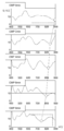
도 7은 연마 정도에 따른 반사광의 스펙트럼을 나타낸 도면이다.
도 8은 본 발명에 따른 두께-스펙트럼 데이터 베이스 생성 방법의 순서도이다.
도 9는 본 발명에 따른 연마 모니터링 방법의 순서도이다.1 is a schematic diagram of a polishing monitoring system according to the present invention.
2 is a block diagram of a polishing monitoring system according to the present invention.
3 is a block diagram of a monitoring unit according to the invention.
4 is a plan view of part A of FIG. 1.
5 is a cross-sectional view of the substrate before polishing.
6 is a cross-sectional view of the substrate after polishing.
7 is a view showing a spectrum of reflected light according to the degree of polishing.
8 is a flowchart of a method for generating a thickness-spectrum database according to the present invention.
9 is a flowchart of a polishing monitoring method according to the present invention.
본 발명의 이점 및 특징, 그리고 그것들을 달성하는 방법은 첨부되는 도면과 함께 상세하게 후술되어 있는 실시예들을 참조하면 명확해질 것이다. 그러나 본 발명은 이하에서 개시되는 실시예들에 한정되는 것이 아니라 서로 다른 다양한 형태로 구현될 것이며, 단지 본 실시예들은 본 발명의 개시가 완전하도록 하며, 본 발명이 속하는 기술분야에서 통상의 지식을 가진 자에게 발명의 범주를 완전하게 알려주기 위해 제공되는 것이며, 본 발명은 청구항의 범주에 의해 정의될 뿐이다. 따라서, 몇몇 실시예에서, 잘 알려진 공정 단계들, 잘 알려진 소자 구조 및 잘 알려진 기술들은 본 발명이 모호하게 해석되는 것을 피하기 위하여 구체적으로 설명되지 않는다. 명세서 전체에 걸쳐 동일 참조 부호는 동일 구성 요소를 지칭한다.Advantages and features of the present invention, and methods for achieving them will be clarified with reference to embodiments described below in detail together with the accompanying drawings. However, the present invention is not limited to the embodiments disclosed below, but will be implemented in various different forms, and only the embodiments allow the disclosure of the present invention to be complete, and the ordinary knowledge in the technical field to which the present invention pertains. It is provided to fully inform the holder of the scope of the invention, and the invention is only defined by the scope of the claims. Thus, in some embodiments, well-known process steps, well-known device structures, and well-known techniques are not specifically described to avoid obscuring the present invention. The same reference numerals refer to the same components throughout the specification.
도면에서 여러 층 및 영역을 명확하게 표현하기 위하여 두께를 확대하여 나타내었다. 명세서 전체를 통하여 유사한 부분에 대해서는 동일한 도면 부호를 붙였다. 층, 막, 영역, 판 등의 부분이 다른 부분 "위에" 있다고 할 때, 이는 다른 부분 "바로 위에" 있는 경우뿐 아니라 그 중간에 또 다른 부분이 있는 경우도 포함한다. 반대로 어떤 부분이 다른 부분 "바로 위에" 있다고 할 때에는 중간에 다른 부분이 없는 것을 뜻한다. 또한, 층, 막, 영역, 판 등의 부분이 다른 부분 "아래에" 있다고 할 때, 이는 다른 부분 "바로 아래에" 있는 경우뿐 아니라 그 중간에 또 다른 부분이 있는 경우도 포함한다. 반대로 어떤 부분이 다른 부분 "바로 아래에" 있다고 할 때에는 중간에 다른 부분이 없는 것을 뜻한다.In the drawings, the thickness is enlarged to clearly express the various layers and regions. The same reference numerals are used for similar parts throughout the specification. When a portion of a layer, film, region, plate, etc. is said to be “above” another portion, this includes not only the case “directly above” another portion, but also another portion in between. Conversely, when one part is "just above" another part, it means that there is no other part in the middle. Further, when a part such as a layer, film, region, plate, etc. is said to be "below" another part, this includes the case where another part is "just below" as well as another part in the middle. Conversely, when one part is "just below" another part, it means that there is no other part in the middle.
공간적으로 상대적인 용어인 "아래(below)", "아래(beneath)", "하부(lower)", "위(above)", "상부(upper)" 등은 도면에 도시되어 있는 바와 같이 하나의 소자 또는 구성 요소들과 다른 소자 또는 구성 요소들과의 상관관계를 용이하게 기술하기 위해 사용될 수 있다. 공간적으로 상대적인 용어는 도면에 도시되어 있는 방향에 더하여 사용시 또는 동작시 소자의 서로 다른 방향을 포함하는 용어로 이해되어야 한다. 예를 들면, 도면에 도시되어 있는 소자를 뒤집을 경우, 다른 소자의 "아래(below)"또는 "아래(beneath)"로 기술된 소자는 다른 소자의 "위(above)"에 놓여질 수 있다. 따라서, 예시적인 용어인 "아래"는 아래와 위의 방향을 모두 포함할 수 있다. 소자는 다른 방향으로도 배향될 수 있고, 이에 따라 공간적으로 상대적인 용어들은 배향에 따라 해석될 수 있다.The spatially relative terms “below”, “beneath”, “lower”, “above”, “upper”, etc., are as shown in the figure. It can be used to easily describe the correlation of a device or components with other devices or components. The spatially relative terms should be understood as terms including different directions of the device in use or operation in addition to the directions shown in the drawings. For example, if the device shown in the figure is turned over, the device described as "below" or "beneath" the other device may be placed "above" the other device. Accordingly, the exemplary term “below” can include both the directions below and above. The device can also be oriented in other directions, so that spatially relative terms can be interpreted according to the orientation.
본 명세서에서 어떤 부분이 다른 부분과 연결되어 있다고 할 때, 이는 직접적으로 연결되어있는 경우뿐 아니라, 그 중간에 다른 소자를 사이에 두고 전기적으로 연결되어 있는 경우도 포함한다. 또한, 어떤 부분이 어떤 구성 요소를 포함한다고 할 때, 이는 특별히 그에 반대되는 기재가 없는 한 다른 구성요소를 제외하는 것이 아니라 다른 구성요소를 더 포함할 수 있는 것을 의미한다.In the present specification, when a part is connected to another part, this includes not only the case of being directly connected, but also the case of being electrically connected with another element in between. In addition, when a part includes a certain component, this means that other components may be further included instead of excluding other components unless otherwise specified.
본 명세서에서 제 1, 제 2, 제 3 등의 용어는 다양한 구성 요소들을 설명하는데 사용될 수 있지만, 이러한 구성 요소들은 상기 용어들에 의해 한정되는 것은 아니다. 상기 용어들은 하나의 구성 요소를 다른 구성 요소들로부터 구별하는 목적으로 사용된다. 예를 들어, 본 발명의 권리 범위로부터 벗어나지 않고, 제 1 구성 요소가 제 2 또는 제 3 구성 요소 등으로 명명될 수 있으며, 유사하게 제 2 또는 제 3 구성 요소도 교호적으로 명명될 수 있다.In the present specification, terms such as first, second, and third may be used to describe various components, but these components are not limited by the terms. The terms are used to distinguish one component from other components. For example, without departing from the scope of the present invention, the first component may be referred to as a second or third component, etc., and similarly, the second or third component may also be alternately named.
다른 정의가 없다면, 본 명세서에서 사용되는 모든 용어(기술 및 과학적 용어를 포함)는 본 발명이 속하는 기술분야에서 통상의 지식을 가진 자에게 공통적으로 이해될 수 있는 의미로 사용될 수 있을 것이다. 또 일반적으로 사용되는 사전에 정의되어 있는 용어들은 명백하게 특별히 정의되어 있지 않은 한 이상적으로 또는 과도하게 해석되지 않는다.Unless otherwise defined, all terms (including technical and scientific terms) used in the present specification may be used as meanings commonly understood by those skilled in the art to which the present invention pertains. Also, terms defined in the commonly used dictionary are not ideally or excessively interpreted unless explicitly defined.
이하, 도 1 내지 도 4를 참조하여, 본 발명의 실시예에 따른 연마 모니터링 시스템에 대해 상세히 설명한다.Hereinafter, a polishing monitoring system according to an embodiment of the present invention will be described in detail with reference to FIGS. 1 to 4.
도 1은 본 발명에 따른 연마 모니터링 시스템에 대한 개략도이고, 도 2는 본 발명에 따른 연마 모니터링 시스템의 블록도이다. 도 3은 본 발명에 따른 모니터링 유닛(50)의 블록이고, 도 4는 도 1의 A부분의 평면도이다.1 is a schematic diagram of a polishing monitoring system according to the present invention, and FIG. 2 is a block diagram of a polishing monitoring system according to the present invention. 3 is a block of a
도 1 및 도 2를 참조하면, 본 발명에 따른 연마 모니터링 시스템은 기판 이동 유닛(10), 연마 유닛(20), 세정 유닛(30), 건조 유닛(40), 모니터링 유닛(50), 제어 유닛(60) 및 두께-스펙트럼 데이터 베이스(70)를 포함한다.1 and 2, the polishing monitoring system according to the present invention includes a
기판 이동 유닛(10)은 기판 이동 유닛(10) 상에 배치된 기판(100)을 제1 방향(D1)을 따라 이동시킨다. 예를 들어, 기판 이동 유닛(10)은 컨베이어 장치일 수 있으며, 기판 이동 유닛(10)은 복수의 회전 부재(11) 및 컨베이어 벨트(12)를 포함할 수 있다. 이때, 복수의 회전 부재(11)는 컨베이어 벨트(12)를 제1 방향(D1)을 따라 이동시킬 수 있어, 컨베이어 벨트(12) 상에 배치된 기판(100)을 제1 방향(D1)을 따라 이동시킨다.The
기판 이동 유닛(10)은 일체로 형성되어 연마 유닛(20), 세정 유닛(30), 건조 유닛(40) 및 모니터링 유닛(50) 하에 배치될 수 있다. 다만, 이에 한정되는 것은 아니며, 기판 이동 유닛(10)은 복수 개일 수 있다.The
연마 유닛(20)은 기판 이동 유닛(10) 상에 배치된 기판(100)의 상면을 연마한다. 예를 들어, 연마 유닛(20)은 화학적 기계적 연마(Chemical Mechanical Polishing) 장치일 수 있다. 도시되지 않았지만, 구체적으로 연마 유닛(20)은 연마 테이블, 플래튼 및 슬러리 공급부를 포함할 수 있다.The polishing
연마 테이블은 연마 패드를 포함하고, 연마 패드가 안착되는 회전 가능한 디스크 형상을 가질 수 있다. 연마 테이블은 축에 대하여 회전하도록 작동할 수 있다. 예를 들어, 모터는 구동 샤프트를 회전시켜 연마 테이블을 회전시킬 수 있다.The polishing table includes a polishing pad and may have a rotatable disk shape on which the polishing pad is seated. The polishing table can operate to rotate about an axis. For example, the motor may rotate the drive shaft to rotate the polishing table.
플래튼은 기판 이동 유닛(10)의 컨베이어 벨트(12) 하에 위치하여 연마 테이블이 적용될 수 있도록 기판(100)을 지지한다.The platen is located under the
슬러리 공급부는 연마 패드 상으로 화학 기계적 연마 공정에 필요한 슬러리 용액을 공급할 수 있다. 기판 이동 유닛(10) 상에 배치된 기판(100)은 슬러리 용액의 존재하에서 연마 패드와의 슬라이딩 접촉에 의해 연마될 수 있다.The slurry supply unit may supply the slurry solution required for the chemical mechanical polishing process onto the polishing pad. The
세정 유닛(30)은 기판 이동 유닛(10) 상에서 연마 유닛(20)과 건조 유닛(40) 사이에 배치된다. 세정 유닛(30)은 연마에 의해 기판(100)에 발생한 이물을 제거하기 위해 세정액, 예를 들어 초순수(De-ionized Water; DI)을 분사하여 세척할 수 있다. The
건조 유닛(40)은 기판 이동 유닛(10) 상에서 세정 유닛(30)과 모니터링 유닛(50) 사이에 배치된다. 건조 유닛(40)은 세척된 기판(100)에 잔류하는 세정액을 제거한다. 건조 유닛(40)은 예를 들어 에어부, 흡입부, 건조부 및 언로딩 헤드를 포함할 수 있다.The drying
에어부는 에어나이프를 이용하여 공기를 분사하여 기판(100)에 잔류하는 세정액을 제거한다. 이때, 에어나이프는 다양한 구조의 에어 분사기일 수 있고, 상온의 공기를 분사할 수 있다. 다만, 이에 한정되는 것은 아니다. 흡착부는 기판(100)에 잔류하는 세정액을 석션을 통해 제거한다. 건조부는 열풍 건조로 기판(100)의 상면 또는 하면에 잔류하는 습기를 최종적으로 건조시킨다.The air part blows air using an air knife to remove the cleaning solution remaining on the
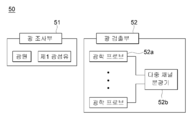
모니터링 유닛(50)은 기판(100)으로부터 반사된 광을 입력 받는다. 구체적으로, 모니터링 유닛(50)은 광 조사부(51) 및 광 검출부(52)를 포함한다. 광 조사부(51)는 기판(100) 상에 광을 조사한다. 이를 위해, 광 조사부(51)는 광원 및 제1 광섬유를 포함할 수 있다. 이때, 광원은 적외선 또는 가시광선을 발광할 수 있다.The
광 검출부(52)는 기판(100)의 서로 다른 위치로부터 반사된 광을 각각 입력 받는다. 이를 위해, 광 검출부(52)는 복수의 광학 프로브(52a)들 및 다중 채널 분광기(Multichannel Spectrometer)(52b)를 포함할 수 있다. The
각각의 광학 프로브(52a)는 다중 채널 분광기(52b)와 연결하기 위한 제2 광섬유를 포함할 수 있다. 이에 따라, 광학 프로브(52a)에서 입력된 기판(100)의 반사광은 제2 광섬유를 통해 다중 채널 분광기(52b)에 입력될 수 있다.Each
다중 채널 분광기(52b)는 복수의 광학 프로브(52a)들을 통해 반사된 광을 각각 입력 받는다. 구체적으로, 다중 채널 분광기(52b)는 입력된 반사광을 파장에 따라 분해하여, 소정의 파장 범위에 걸쳐 광도를 측정한다. 예를 들어, 다중 채널 분광기(52b)는 입력된 반사광을 400nm 내지 900nm의 각각의 파장에 따라 분광하여 스펙트럼을 산출한다. 다만, 이에 한정되는 것은 아니며, 400nm이하 또는 900nm 이상의 파장 범위에 대해 광도를 측정할 수도 있다.The
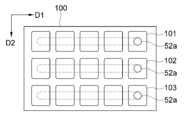
본 발명의 실시예에 따르면, 복수의 광학 프로브(52a)는 제1 방향(D1)과 수직하는 제2 방향(D2)을 따라 배열된다. 구체적으로, 기판(100)은 복수의 셀(101, 102, 103)을 포함할 수 있으며, 복수의 광학 프로브(52a)는 기판(100)의 복수의 셀(101, 102, 103)에 각각 대응하여 배치될 수 있다. 예를 들어, 도 4에 도시된 바와 같이, 3개의 셀(101, 102, 103) 상에 각각 하나의 광학 프로브(52a)가 제2 방향(D2)을 따라 배열될 수 있다. 다만, 광학 프로브(52a)의 개수는 이에 한정되지 아니하며, 제2 방향(D2)을 따라 배열된 셀(101, 102, 103)의 개수에 따라 달라질 수 있다. According to an embodiment of the present invention, the plurality of
기판(100)은 기판 이동 유닛(10)에 의해 제1 방향(D1)을 따라 일정한 속도로 이동할 수 있으며, 광학 프로브(52a)는 제2 방향(D2)에 따라 서로 이격되어 배열되기 때문에, 도 3에 도시된 바와 같이, 기판(100)의 넓은 영역에서 측정된 반사광에 대한 스펙트럼을 산출할 수 있다. 따라서, 본 발명에 따른 연마 모니터링 방법은 제2 무기막(도 5의 120)의 균일성을 정확하게 측정할 수 있다. The
본 발명의 실시예에 따르면, 연마 유닛(20), 세정 유닛(30), 건조 유닛(40) 및 모니터링 유닛(50)은 제1 방향(D1)에 따라 순차적으로 배열된다. 이에 따라, 연마 유닛(20), 세정 유닛(30), 건조 유닛(40) 및 모니터링 유닛(50)의 각 공정은 기판 이동 유닛(10)에 의해 제1 방향(D1)을 따라 이동되는 기판(100)에 순차적으로 적용된다.According to an embodiment of the present invention, the polishing
제어 유닛(60)은 기판 이동 유닛(10), 연마 유닛(20), 세정 유닛(30), 건조 유닛(40) 및 모니터링 유닛(50)의 작동을 제어할 수 있다. The
제어 유닛(60)은 기판(100의 이동 속도를 제어할 수 있다. 구체적으로, 기판 이동 유닛(10)의 회전 부재(11)의 회전 속도를 제어하여 기판 이동 유닛(10)의 컨베이어 벨트(12)의 이동 속도를 조절할 수 있다.The
본 발명의 실시예에 따르면, 제어 유닛(60)은 두께-스펙트럼 데이터 베이스(70)로부터 연마 공정의 종료점(end point)을 산출하여 연마 유닛(20)의 작동 시간을 제어할 수 있다. According to an embodiment of the present invention, the
제어 유닛(60)은 연마 시간에 따라 세정 유닛(30) 및 건조 유닛(40)의 작동 시간을 조절할 수 있다.The
본 발명의 실시예에 따르면, 제어 유닛(60)은 모니터링 유닛(50)으로부터 산출된 스펙트럼과 기준 스펙트럼을 비교하여 연마 공정의 종료점 및 제2 무기막(120)의 두께를 산출할 수 있다. 예를 들어, 제어 유닛(60)은 기준 스펙트럼들 중 모니터링 유닛(50)에 의해 산출된 스펙트럼의 피크(peak)점 또는 밸리(valley)점에서의 파장과 동일한 파장에서 피크(peak)점 또는 밸리(valley)점을 갖는 기준 스펙트럼을 검색하여 제2 무기막(120)의 두께를 산출할 수 있다. 본 발명의 실시예에 따르면 연마 공정의 종료점(end-point)을 정확하게 산출할 수 있다.According to an embodiment of the present invention, the
두께-스펙트럼 데이터 베이스(70)는 연마 공정이 적용된 제2 무기막(120)의 두께에 따른 스펙트럼 및 연마 시간에 관한 데이터를 포함한다. 이에 대해서는 도 5 내지 도 9를 참조하여 상세히 설명한다.The thickness-
이하, 도 5 내지 도 7을 참조하여, 본 발명에 따른 연마 모니터링 방법의 원리에 대해 상세히 설명한다.Hereinafter, the principle of the polishing monitoring method according to the present invention will be described in detail with reference to FIGS. 5 to 7.
도 5는 연마 전 기판의 단면도이고, 도 6은 연마 후 기판의 단면도이고, 도 7은 연마 정도에 따른 반사광의 스펙트럼을 나타낸 도면이다.5 is a cross-sectional view of the substrate before polishing, FIG. 6 is a cross-sectional view of the substrate after polishing, and FIG. 7 is a view showing a spectrum of reflected light according to the polishing degree.
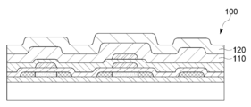
도 5 및 도 6을 참조하면, 본 발명에 따른 연마 공정이 적용되는 기판(100)은 표시 화소를 포함하는 표시 기판으로, 액정 표시 기판 또는 유기 발광 표시 기판 중 어느 하나일 수 있다. 구체적으로, 도 5에 도시된 바와 같이, 연마 공정이 적용되는 기판(100)은 복수의 패턴을 포함할 수 있으며, 패턴을 순차적으로 덮는 제1 무기막(110) 및 제2 무기막(120)을 포함할 수 있다. 이에 따라, 기판에 포함된 패턴에 의해 제1 무기막(110) 및 제2 무기막(120)은 각각 단차를 가질 수 있다.5 and 6, the
제1 무기막(110) 및 제2 무기막(120)은 각각 실리콘 산화물(SiOx) 또는 실리콘 질화물(SiNx)을 포함할 수 있다. 또한, 제1 무기막(110) 및 제2 무기막(120)은 각각 산화 알루미늄, 산화 티타늄, 산화 탄탈륨 또는 산화 지르코늄을 더 포함할 수 있다. 예를 들어, 제1 무기막(110)은 실리콘 질화물(SiNx)이고, 제2 무기막(120)은 실리콘 산화물(SiOx)일 수 있다. The first
연마 공정이 제1 무기막(110) 및 제2 무기막(120)을 포함하는 기판(100)에 적용되면, 도 6에 도시된 바와 같이, 제2 무기막(120)의 일부가 제거되어 제1 무기막(110) 및 제2 무기막(120)의 일부를 포함하는 기판(100)의 상면이 평탄화된다. When the polishing process is applied to the
광 조사부(51)로부터 조사된 제1 광(L1)은 복수의 층을 포함하는 기판(100)의 복수의 층의 계면에서 반사되고 간섭되어 제2 광(L2)으로 광 검출부(52)에 입력된다. 제2 광(L2)은 복수의 층의 계면에서 반사되고 간섭된 광이기 때문에, 기판(100)에 위치하는 하나의 층의 두께를 정확하게 측정하기 어렵다. 다만, 기판(100)에 배치된 하나의 층의 두께에 따라 기판(100)의 반사광의 스펙트럼이 달라진다. 구체적으로, 제2 무기막(120)의 두께가 감소할수록, 제2 광(L2)의 파장이 짧아지는 현상이 발생한다. 결과적으로, 연마가 적용되는 시간이 증가할수록 제2 무기막(120)의 두께는 감소하고, 제2 무기막(120)의 두께가 감소할수록 도 7에 도시된 바와 같이, 기판(100)의 반사광 스펙트럼의 파장이 감소한다. 이에 따라, 제2 무기막(120)의 두께에 따라 모니터링 유닛(50)에 의해 산출된 스펙트럼의 피크(peak)점 및 밸리(valley)점에서의 파장이 달라질 수 있다.The first light L1 irradiated from the
본 발명의 실시예는 제2 무기막(120)의 두께에 각각 대응하는 기준 스펙트럼에 대한 데이터를 포함하는 두께-스펙트럼 데이터 베이스를 생성하고, 모니터링 유닛(50)에 의해 산출된 스펙트럼의 피크(peak)점 및 밸리(valley)점의 파장을 분석하여 기준 스펙트럼의 피크(peak)점 및 밸리(valley)점의 파장과 비교하여 제2 무기막(120)의 두께를 산출할 수 있다.An embodiment of the present invention generates a thickness-spectrum database including data for a reference spectrum corresponding to the thickness of the second
이하, 도 8 내지 도 9를 참조하여, 본 발명에 따른 연마 모니터링 방법에 대해 상세히 설명한다.Hereinafter, a polishing monitoring method according to the present invention will be described in detail with reference to FIGS. 8 to 9.
도 8은 본 발명에 따른 두께-스펙트럼 데이터 베이스(70) 생성 방법의 순서도이다.8 is a flowchart of a method for generating a thickness-
본 발명의 실시예에 따르면, 두께-스펙트럼 데이터 베이스(70)를 이용하여 연마 공정의 종료점(end point)을 결정하고 제2 무기막(120)의 두께에 대해 피드백을 진행한다. 이를 위해, 두께-스펙트럼 데이터 베이스(70)를 생성한다.According to an embodiment of the present invention, the end point of the polishing process is determined using the thickness-
우선, 연마 유닛(20)은 제1 무기막(110) 및 제2 무기막(120)을 포함하는 기판(100)에 연마 공정을 적용하여 제2 무기막(120)의 일부를 연마한다. 이에 따라, 도 6에 도시된 바와 같이, 기판(100)은 제2 무기막(120)의 적어도 일부를 포함한다. 이후, 기판(100)은 기판 이동 유닛(10)에 의해 제1 방향(D1)을 따라 세정 유닛(30), 건조 유닛(40) 및 모니터링 유닛(50)을 향해 이동한다. 이에 따라, 기판(100)은 세정 유닛(30) 및 건조 유닛(40)에 의해 세정 및 건조된다. First, the polishing
모니터링 유닛(50)은 기판(100)의 반사광의 스펙트럼을 측정한다(S121). 구체적으로, 광 조사부(51)는 기판(100)에 가시광선 또는 적외선을 조사하고, 광학 프로브(52a)는 기판(100)에서 반사된 가시광선 또는 적외선을 입력 받는다. 다중 채널 분광기(52b)는 입력받은 반사광을 파장에 따라 분해하여 소정의 파장 범위에 걸쳐 광도를 산출할 수 있다.The
이와 함께, 기판(100)의 단면을 투과 전자 현미경(Transmission Electron Microscope)을 통해 잔류하는 제2 무기막(120)의 두께를 측정한다(S122).In addition, the thickness of the second
모니터링 유닛(50)은 제2 무기막(120)의 두께에 각각 대응하는 기준 스펙트럼을 산출할 수 있다. 이에 따라, 제2 무기막(120)의 두께에 각각 대응하는 기준 스펙트럼에 대한 데이터를 포함하는 두께-스펙트럼 데이터 베이스(70)가 생성된다(S13). 이때, 두께-스펙트럼 데이터 베이스(70)는 두께에 각각 대응하는 기준 스펙트럼과 함께 연마 시간을 나타내는 연마 공정의 종료점에 대한 데이터를 포함할 수 있다.The
본 발명의 일 실시예에 따르면, 제어 유닛(60)은 모니터링 유닛(50)에 의해 산출된 스펙트럼을 기준 스펙트럼과 비교하여 제2 무기막(120)의 두께 및 연마 공정의 종료점을 산출할 수 있다. According to an embodiment of the present invention, the
도 9는 본 발명에 따른 연마 모니터링 방법의 순서도이다.9 is a flowchart of a polishing monitoring method according to the present invention.
도 8 및 도 9를 참조하면, 우선 전술한 바와 같이, 두께-스펙트럼 데이터 베이스(70)를 생성한다(S21).8 and 9, first, as described above, the thickness-
두께-스펙트럼 데이터 베이스(70)를 생성한 후, 연마 공정 및 모니터링을 진행한다. 연마 유닛(20)은 기판 이동 유닛(10) 상에 배치된 기판(100)에 대해 연마 공정을 진행한다(S22). 구체적으로, 제어 유닛(60)은 연마 공정의 종료점을 두께-스펙트럼 데이터 베이스(70)로부터 입력 받아 연마 유닛(20)으로 출력하고 이에 따라, 연마 유닛(20)은 연마 공정의 종료점동안 제2 무기막(120)을 연마할 수 있다. 이에 따라, 도 5에 도시된 제2 무기막(120)의 상면이 연마되어, 도 6에 도시된 제2 무기막(120)의 상면과 같이 평탄화될 수 있다. After the thickness-
제2 무기막(120)이 연마된 후, 기판(100)은 기판 이동 유닛(10)에 의해 제1 방향(D1)을 따라 이동되어 세정 유닛(30) 및 건조 유닛(40)을 통해 기판(100)이 세정되고 기판(100)에 잔류하는 세정액을 제거한다.After the second
모니터링 유닛(50)은 기판(100)에 광을 조사하고 반사광을 측정하여 반사광의 스펙트럼을 산출한다(S23). 구체적으로, 광 조사부(51)는 기판(100)에 광을 조사하고, 광학 프로브(52a)는 기판(100)의 반사광을 입력 받는다. 다중 채널 분광기(52b)는 광학 프로브(52a)를 통해 입력된 반사광을 파장에 따라 분해하여 스펙트럼을 산출한다. The
본 발명의 실시예에 따르면, 복수의 광학 프로브(52a)는 기판(100)의 복수의셀(101, 102, 103)에 각각 대응하도록 배열되기 때문에, 모니터링 유닛(50)은 기판(100)의 서로 다른 위치에 대해 동시에 각각의 스펙트럼을 산출한다. 본 발명에 따른 연마 모니터링 방법은 연마 공정이 적용된 제2 무기막(120) 및 제2 무기막(120)을 포함하는 기판(100)의 균일성을 측정할 수 있다. According to an embodiment of the present invention, since the plurality of
제어 유닛(60)은 산출된 반사광의 스펙트럼을 기준 스펙트럼과 비교한다(S24). 예를 들어, 제어 유닛(60)은 기준 스펙트럼들 중 모니터링 유닛(50)에 의해 산출된 스펙트럼의 피크(peak)점 또는 밸리(valley)점에서의 동일한 파장과 동일한 파장에서 피크(peak)점 또는 밸리(valley)점을 갖는 기준 스펙트럼을 검색한다.The
제어 유닛(60)은 제2 무기막(120)의 두께를 산출한다(S25). 구체적으로, 제어 유닛(60)은 모니터링 유닛(50)에 의해 산출된 스펙트럼의 피크(peak)점 또는 밸리(valley)점에서의 파장과 동일한 파장에서 피크(peak)점 또는 밸리(valley)점을 갖는 기준 스펙트럼을 검색하여 이에 대응하는 제2 무기막(120)의 두께를 산출한다.The
제어 유닛(60)은 제2 무기막(120)의 두께가 적절한 두께인지 판단한다(S26). 제2 무기막(120)의 두께가 일정 범위 내에 포함되는 경우 제2 무기막(120)의 두께가 적절한 것으로 판단될 수 있고, 제어 유닛(60)은 연마 모니터링 방법을 종료한다. 제2 무기막(120)의 두께가 일정 범위 내에 포함되지 않는 경우 제2 무기막(120)의 두께가 적절하지 않은 것으로 판단될 수 있고, 이에 따라 추가로 진행되어야 할 연마 시간을 산출하여 연마 공정을 재진행할 수 있다.The
또한, 제어 유닛(60)은 복수의 광학 프로브(52a)에 의해 동시에 각각 측정된 스펙트럼으로부터 산출된 각 두께들을 서로 비교한다. 이를 통해, 제2 무기막(120)의 균일성을 판단할 수 있다. 기판(100)이 균일한 것으로 판단된 경우 제2 무기막(120)의 두께가 적절한 것으로 판단될 수 있고, 제어 유닛(60)은 연마 모니터링 방법을 종료한다. 제2 무기막(120)의 두께가 균일하지 않은 것으로 판단된 경우 제2 무기막(120)의 두께가 적절하지 않은 것으로 판단될 수 있다. 이에 따라, 제어 유닛(60)은 추가로 진행되어야 할 연마 시간을 산출하여 연마 공정을 재진행할 수 있다.In addition, the
이상에서 설명한 본 발명은 상술한 실시예 및 첨부된 도면에 한정되는 것이 아니고, 본 발명의 기술적 사상을 벗어나지 않는 범위 내에서 여러 가지 치환, 변형 및 변경이 가능하다는 것이 본 발명이 속하는 기술 분야에서 통상의 지식을 가진 자에게 있어 명백할 것이다.The present invention described above is not limited to the above-described embodiments and the accompanying drawings, and it is common in the technical field to which the present invention pertains that various substitutions, modifications and changes are possible without departing from the spirit of the present invention It will be clear to those who have the knowledge of
10: 기판 이동 유닛
20: 연마 유닛
30: 세정 유닛
40: 건조 유닛
50: 모니터링 유닛
60: 제어 유닛
70: 두께-스펙트럼 데이터 베이스10: substrate moving unit 20: polishing unit
30: cleaning unit 40: drying unit
50: monitoring unit 60: control unit
70: thickness-spectrum database
Claims (20)
상기 기판 이동 유닛 상에 배치된 연마 유닛;
상기 기판 이동 유닛 상에 배치된 세정 유닛 및 건조 유닛;
상기 기판 이동 유닛 상에 배치되고 기판의 서로 다른 복수의 위치의 반사광을 각각 측정하는 복수의 광학 프로브를 포함하는 모니터링 유닛;
상기 연마 유닛, 상기 세정 유닛, 상기 건조 유닛 및 모니터링 유닛은 상기 제1 방향을 따라 순차적으로 배치된 연마 모니터링 시스템.A substrate moving unit moving the substrate including at least one inorganic film along a first direction;
A polishing unit disposed on the substrate moving unit;
A cleaning unit and a drying unit disposed on the substrate moving unit;
A monitoring unit disposed on the substrate moving unit and including a plurality of optical probes for measuring reflected light at a plurality of different locations on the substrate, respectively;
The polishing unit, the cleaning unit, the drying unit and the monitoring unit are sequentially arranged along the first direction polishing monitoring system.
상기 복수의 광학 프로브는 상기 제1 방향과 수직하는 제2 방향을 따라 서로 이격되어 배열된 연마 모니터링 시스템.According to claim 1,
The plurality of optical probes are spaced apart from each other along a second direction perpendicular to the first direction, the polishing monitoring system.
상기 복수의 광학 프로브는 상기 제1 방향 및 상기 제1 방향과 수직하는 제2 방향에 따라 배열된 복수의 셀을 포함하는 기판의 각 셀에 대응하도록 배치된 연마 모니터링 시스템.According to claim 1,
The plurality of optical probes are arranged to correspond to each cell of the substrate including a plurality of cells arranged along the first direction and a second direction perpendicular to the first direction.
상기 무기막의 두께 및 상기 무기막의 두께와 대응하는 기준 스펙트럼으로 이루어진 데이터를 포함하는 두께-스펙트럼 데이터 베이스를 포함하는 연마 모니터링 시스템.According to claim 1,
A polishing monitoring system comprising a thickness-spectrum database including data consisting of a thickness of the inorganic film and a reference spectrum corresponding to the thickness of the inorganic film.
상기 두께-스펙트럼 데이터 베이스는 상기 무기막의 두께에 대응하는 연마 시간에 대한 데이터를 포함하는 연마 모니터링 시스템.The method of claim 4,
The thickness-spectrum database includes a polishing time data corresponding to the thickness of the inorganic film.
상기 복수의 광학 프로브와 연결되고, 상기 복수의 광학 프로브로부터 각각 측정된 반사광으로부터 스펙트럼을 각각 산출하는 다중 채널 분광기를 포함하는 연마 모니터링 시스템.The method of claim 4,
A polishing monitoring system comprising a multi-channel spectrometer connected to the plurality of optical probes and calculating a spectrum from reflected light respectively measured from the plurality of optical probes.
상기 산출된 복수의 스펙트럼을 상기 기준 스펙트럼과 비교하는 제어 유닛을 더 포함하는 연마 모니터링 시스템. The method of claim 6,
And a control unit that compares the calculated plurality of spectra with the reference spectrum.
상기 제어 유닛은 상기 다중 채널 분광기로부터 산출된 스펙트럼의 피크(peak)점 및 밸리(valley)점에서의 파장과 상기 기준 스펙트럼의 피크점 및 밸리점에서의 파장을 각각 비교하는 연마 모니터링 시스템.The method of claim 7,
The control unit is a polishing monitoring system that compares the wavelengths at the peak and valley points of the spectrum calculated from the multi-channel spectrometer, respectively, and the wavelengths at the peak and valley points of the reference spectrum.
상기 제어 유닛은 상기 산출된 복수의 스펙트럼을 서로 비교하는 연마 모니터링 시스템.The method of claim 7,
The control unit compares the calculated plurality of spectra to each other a polishing monitoring system.
적어도 하나의 무기막을 포함하는 기판에 대해 연마 공정을 진행하는 단계;
상기 기판의 서로 다른 복수의 위치에 대해 동시에 각각의 스펙트럼을 산출하는 단계;
상기 산출된 각각의 스펙트럼과 두께-스펙트럼 데이터 베이스에 포함된 기준 스펙트럼과 비교하는 단계;
상기 기판의 서로 다른 복수의 위치에 대한 무기막의 두께를 각각 산출하는 단계; 및
상기 기판의 서로 다른 복수의 위치에 대한 무기막의 두께의 적절성을 판단하는 단계;를 포함하는 연마 모니터링 방법.Creating a thickness-spectrum database;
Performing a polishing process on a substrate including at least one inorganic film;
Calculating respective spectra simultaneously for a plurality of different positions of the substrate;
Comparing each of the calculated spectrum and a reference spectrum included in a thickness-spectrum database;
Calculating thicknesses of inorganic films for a plurality of different positions of the substrate, respectively; And
Determining the appropriateness of the thickness of the inorganic film for a plurality of different positions of the substrate; polishing monitoring method comprising a.
상기 기판의 서로 다른 복수의 위치에 대해 동시에 각각의 스펙트럼을 산출하는 단계는,
상기 기판의 서로 다른 복수의 위치는 상기 기판에 포함된 복수의 셀에 각각 대응하는 연마 모니터링 방법.The method of claim 10,
The step of simultaneously calculating the respective spectra for a plurality of different positions of the substrate may include:
A plurality of different positions of the substrate corresponding to the polishing monitoring method respectively corresponding to a plurality of cells included in the substrate.
상기 기판의 서로 다른 위치에 대한 무기막의 두께의 적절성을 판단하는 단계는,
상기 기판의 서로 다른 위치에 대해 산출된 각각의 두께를 서로 비교하는 단계; 및
상기 무기막의 균일성을 판단하는 단계;를 포함하는 연마 모니터링 방법.The method of claim 10,
Determining the appropriateness of the thickness of the inorganic film for different positions of the substrate,
Comparing each thickness calculated for different positions of the substrate with each other; And
Determining the uniformity of the inorganic film; Polishing monitoring method comprising a.
상기 두께-스펙트럼 데이터 베이스는 상기 무기막의 두께 및 상기 무기막의 두께와 대응하는 기준 스펙트럼에 대한 데이터를 포함하는 연마 모니터링 방법.The method of claim 10,
The thickness-spectrum database includes a thickness of the inorganic film and the data for the reference spectrum corresponding to the thickness of the inorganic film polishing monitoring method.
상기 두께-스펙트럼 데이터 베이스는 상기 무기막의 두께에 대응하는 연마 시간에 대한 데이터를 포함하는 연마 모니터링 방법.The method of claim 10,
The thickness-spectrum database includes polishing time data corresponding to the thickness of the inorganic film.
상기 기판의 서로 다른 복수의 위치에 대해 동시에 각각의 스펙트럼을 산출하는 단계는,
상기 기판의 서로 다른 복수의 위치에서 상기 기판의 반사광을 각각 측정하는 단계; 및
상기 각각 측정된 기판의 반사광을 파장에 따라 분해하는 단계;를 포함하는 연마 모니터링 방법.The method of claim 10,
The step of simultaneously calculating the respective spectra for a plurality of different positions of the substrate may include:
Measuring reflected light of the substrate at a plurality of different locations of the substrate, respectively; And
Decomposing the reflected light of each of the measured substrate according to the wavelength; Polishing monitoring method comprising a.
상기 산출된 각각의 스펙트럼과 두께-스펙트럼 데이터 베이스에 포함된 기준 스펙트럼과 비교하는 단계는,
각각 산출된 스펙트럼의 피크(peak)점 및 밸리(valley)점에서의 파장과 상기 기준 스펙트럼의 피크점 및 밸리점에서의 파장을 각각 비교하는 단계;를 더 포함하는 연마 모니터링 방법.The method of claim 10,
Comparing each of the calculated spectrum and the reference spectrum included in the thickness-spectrum database,
And comparing the wavelengths at the peak and valley points of the spectrum, respectively, and the wavelengths at the peak and valley points of the reference spectrum, respectively.
상기 기판의 서로 다른 복수의 위치에 대해 동시에 각각의 스펙트럼을 산출하는 단계는,
상기 각각 측정된 반사광을 400nm 이상 900nm 이하의 파장에 따라 광도를 측정하는 연마 모니터링 방법.The method of claim 10,
The step of simultaneously calculating the respective spectra for a plurality of different positions of the substrate may include:
Polishing monitoring method for measuring the measured light intensity according to the wavelength of each of the 400nm or more and 900nm or less.
상기 두께-스펙트럼 데이터 베이스를 생성하는 단계는,
적어도 하나의 무기막을 포함하는 복수의 기판에 대해 연마 공정을 각각 진행하는 단계;
상기 복수의 기판 중 각각의 기판에 대한 스펙트럼을 산출하는 단계;
상기 복수의 기판 중 각각의 기판의 상기 무기막의 두께를 투과 전자 현미경을 통해 측정하는 단계; 및
상기 무기막의 두께 및 상기 무기막의 두께에 대응하는 각각의 기판에 대한 기준 스펙트럼을 산출하는 단계;를 포함하는 연마 모니터링 방법.The method of claim 10,
The step of creating the thickness-spectrum database includes:
Performing a polishing process on a plurality of substrates each including at least one inorganic film;
Calculating a spectrum for each of the plurality of substrates;
Measuring the thickness of the inorganic film of each of the plurality of substrates through a transmission electron microscope; And
And calculating a reference spectrum for each substrate corresponding to the thickness of the inorganic film and the thickness of the inorganic film.
상기 복수의 기판 중 각각의 기판에 대한 스펙트럼을 산출하는 단계;
상기 복수의 기판 중 각각의 기판의 무기막의 두께를 투과 전자 현미경을 통해 측정하는 단계; 및
상기 무기막의 두께 및 상기 무기막의 두께에 대응하는 각각의 기판에 대한 기준 스펙트럼을 산출하는 단계; 를 포함하는 연마 모니터링 방법.Performing a polishing process on a plurality of substrates each including at least one inorganic film;
Calculating a spectrum for each of the plurality of substrates;
Measuring the thickness of the inorganic film of each of the plurality of substrates through a transmission electron microscope; And
Calculating a reference spectrum for each substrate corresponding to the thickness of the inorganic film and the thickness of the inorganic film; Polishing monitoring method comprising a.
상기 무기막의 두께 및 상기 무기막의 두께에 대응하는 각각의 기판에 대한 기준 스펙트럼을 산출하는 단계는,
상기 무기막의 두께에 대응하는 상기 기준 스펙트럼의 피크(peak)점 및 밸리(valley)점에서의 파장을 산출하는 단계;를 포함하는 연마 모니터링 방법.The method of claim 19,
Computing a reference spectrum for each substrate corresponding to the thickness of the inorganic film and the thickness of the inorganic film,
And calculating a wavelength at a peak point and a valley point of the reference spectrum corresponding to the thickness of the inorganic film.
Priority Applications (3)
| Application Number | Priority Date | Filing Date | Title |
|---|---|---|---|
| KR1020180155045A KR20200068785A (en) | 2018-12-05 | 2018-12-05 | Apparatus and metheod for monitoring of chemical mechanical polishing |
| US16/582,658 US20200180103A1 (en) | 2018-12-05 | 2019-09-25 | Apparatus and method for monitoring chemical mechanical polishing |
| CN201911233241.XA CN111267000A (en) | 2018-12-05 | 2019-12-05 | Apparatus and method for monitoring polishing |
Applications Claiming Priority (1)
| Application Number | Priority Date | Filing Date | Title |
|---|---|---|---|
| KR1020180155045A KR20200068785A (en) | 2018-12-05 | 2018-12-05 | Apparatus and metheod for monitoring of chemical mechanical polishing |
Publications (1)
| Publication Number | Publication Date |
|---|---|
| KR20200068785A true KR20200068785A (en) | 2020-06-16 |
Family
ID=70970595
Family Applications (1)
| Application Number | Title | Priority Date | Filing Date |
|---|---|---|---|
| KR1020180155045A KR20200068785A (en) | 2018-12-05 | 2018-12-05 | Apparatus and metheod for monitoring of chemical mechanical polishing |
Country Status (3)
| Country | Link |
|---|---|
| US (1) | US20200180103A1 (en) |
| KR (1) | KR20200068785A (en) |
| CN (1) | CN111267000A (en) |
Cited By (1)
| Publication number | Priority date | Publication date | Assignee | Title |
|---|---|---|---|---|
| CN113560962A (en) * | 2021-07-28 | 2021-10-29 | 安徽鸿海新材料股份有限公司 | Preparation method of copper-clad plate with excellent thickness range |
Families Citing this family (2)
| Publication number | Priority date | Publication date | Assignee | Title |
|---|---|---|---|---|
| KR20200130545A (en) * | 2019-05-08 | 2020-11-19 | 삼성디스플레이 주식회사 | Apparatus and method for manufacturing a display apparatus |
| CN112355849A (en) * | 2020-10-15 | 2021-02-12 | 深圳市鑫达辉软性电路科技有限公司 | Physical oxidation cleaning machine |
Family Cites Families (17)
| Publication number | Priority date | Publication date | Assignee | Title |
|---|---|---|---|---|
| JPH0199229A (en) * | 1987-10-13 | 1989-04-18 | Nec Corp | Belt conveyor for semiconductor wafer |
| US6111634A (en) * | 1997-05-28 | 2000-08-29 | Lam Research Corporation | Method and apparatus for in-situ monitoring of thickness using a multi-wavelength spectrometer during chemical-mechanical polishing |
| US6273796B1 (en) * | 1999-09-01 | 2001-08-14 | Micron Technology, Inc. | Method and apparatus for planarizing a microelectronic substrate with a tilted planarizing surface |
| US6270620B1 (en) * | 1999-09-14 | 2001-08-07 | World Wiser Electronics Inc. | Etching device |
| JP3854056B2 (en) * | 1999-12-13 | 2006-12-06 | 株式会社荏原製作所 | Substrate film thickness measuring method, substrate film thickness measuring apparatus, substrate processing method, and substrate processing apparatus |
| US6447374B1 (en) * | 1999-12-17 | 2002-09-10 | Applied Materials, Inc. | Chemical mechanical planarization system |
| US6616801B1 (en) * | 2000-03-31 | 2003-09-09 | Lam Research Corporation | Method and apparatus for fixed-abrasive substrate manufacturing and wafer polishing in a single process path |
| JP5027377B2 (en) * | 2001-06-26 | 2012-09-19 | アプライド マテリアルズ インコーポレイテッド | Endpoint detection system for chemical mechanical polishing |
| US6562185B2 (en) * | 2001-09-18 | 2003-05-13 | Advanced Micro Devices, Inc. | Wafer based temperature sensors for characterizing chemical mechanical polishing processes |
| KR100808829B1 (en) * | 2002-12-26 | 2008-03-07 | 램 리써치 코포레이션 | Chemical mechanical polishing system, methods for monitoring a process state of a wafer surface, and end-point detection method |
| JP4863726B2 (en) * | 2006-02-03 | 2012-01-25 | 株式会社リコー | Fixing device, image forming apparatus |
| JP5612945B2 (en) * | 2010-07-23 | 2014-10-22 | 株式会社荏原製作所 | Method and apparatus for monitoring progress of substrate polishing |
| JP5980476B2 (en) * | 2010-12-27 | 2016-08-31 | 株式会社荏原製作所 | Polishing apparatus and polishing method |
| JP5798505B2 (en) * | 2011-04-27 | 2015-10-21 | 株式会社Screenホールディングス | Substrate processing apparatus and substrate processing method |
| US9067295B2 (en) * | 2012-07-25 | 2015-06-30 | Applied Materials, Inc. | Monitoring retaining ring thickness and pressure control |
| CN106457507B (en) * | 2014-04-22 | 2019-04-09 | 株式会社荏原制作所 | Grinding method |
| CN106217232B (en) * | 2016-08-31 | 2018-08-17 | 广州创芯旗自动化控制设备有限公司 | A kind of super-precision grinding grinding machine |
-
2018
- 2018-12-05 KR KR1020180155045A patent/KR20200068785A/en not_active Application Discontinuation
-
2019
- 2019-09-25 US US16/582,658 patent/US20200180103A1/en not_active Abandoned
- 2019-12-05 CN CN201911233241.XA patent/CN111267000A/en active Pending
Cited By (1)
| Publication number | Priority date | Publication date | Assignee | Title |
|---|---|---|---|---|
| CN113560962A (en) * | 2021-07-28 | 2021-10-29 | 安徽鸿海新材料股份有限公司 | Preparation method of copper-clad plate with excellent thickness range |
Also Published As
| Publication number | Publication date |
|---|---|
| US20200180103A1 (en) | 2020-06-11 |
| CN111267000A (en) | 2020-06-12 |
Similar Documents
| Publication | Publication Date | Title |
|---|---|---|
| US9969048B2 (en) | Polishing apparatus | |
| US7840375B2 (en) | Methods and apparatus for generating a library of spectra | |
| JP5774059B2 (en) | Determination of polishing end point using spectrum | |
| US9496190B2 (en) | Feedback of layer thickness timing and clearance timing for polishing control | |
| KR101669554B1 (en) | Method of monitoring progress of substrate polishing and polishing apparatus | |
| KR20200068785A (en) | Apparatus and metheod for monitoring of chemical mechanical polishing | |
| KR100305537B1 (en) | Polishing method and polishing device using it | |
| US8951813B2 (en) | Method of polishing a substrate having a film on a surface of the substrate for semiconductor manufacturing | |
| TWI602644B (en) | Reflectivity measurements during polishing using a camera | |
| US20150017880A1 (en) | Film-thickness measuring apparatus, film-thickness measuring method, and polishing apparatus having the film-thickness measuring apparatus | |
| US20070224915A1 (en) | Substrate thickness measuring during polishing | |
| KR20140135812A (en) | Fitting of optical model to measured spectrum | |
| CN117001534A (en) | Machine vision as input to CMP process control algorithm | |
| US20140078495A1 (en) | Inline metrology for attaining full wafer map of uniformity and surface charge | |
| JP6292819B2 (en) | Endpoint determination using selective spectral monitoring | |
| JPH09298176A (en) | Polishing method and device therefor | |
| KR20210097813A (en) | Preston Matrix Generator | |
| US11195729B2 (en) | Substrate polishing apparatus and method | |
| US20140080229A1 (en) | Adaptive semiconductor processing using feedback from measurement devices | |
| US10978321B2 (en) | Method and system for processing patterned structures | |
| US20140242877A1 (en) | Spectrographic metrology with multiple measurements | |
| JPH09298174A (en) | Polishing method and device therefor | |
| JP7472111B2 (en) | Machine Vision as Input to CMP Process Control Algorithms | |
| JPH09298175A (en) | Polishing method and device therefor |
Legal Events
| Date | Code | Title | Description |
|---|---|---|---|
| A201 | Request for examination | ||
| E902 | Notification of reason for refusal | ||
| AMND | Amendment | ||
| E601 | Decision to refuse application | ||
| X091 | Application refused [patent] |