JP5774059B2 - Determination of polishing end point using spectrum - Google Patents
Determination of polishing end point using spectrum Download PDFInfo
- Publication number
- JP5774059B2 JP5774059B2 JP2013127106A JP2013127106A JP5774059B2 JP 5774059 B2 JP5774059 B2 JP 5774059B2 JP 2013127106 A JP2013127106 A JP 2013127106A JP 2013127106 A JP2013127106 A JP 2013127106A JP 5774059 B2 JP5774059 B2 JP 5774059B2
- Authority
- JP
- Japan
- Prior art keywords
- spectrum
- spectra
- library
- substrate
- rotation
- Prior art date
- Legal status (The legal status is an assumption and is not a legal conclusion. Google has not performed a legal analysis and makes no representation as to the accuracy of the status listed.)
- Active
Links
Images


Classifications
-
- H—ELECTRICITY
- H10—SEMICONDUCTOR DEVICES; ELECTRIC SOLID-STATE DEVICES NOT OTHERWISE PROVIDED FOR
- H10P—GENERIC PROCESSES OR APPARATUS FOR THE MANUFACTURE OR TREATMENT OF DEVICES COVERED BY CLASS H10
- H10P52/00—Grinding, lapping or polishing of wafers, substrates or parts of devices
-
- H—ELECTRICITY
- H10—SEMICONDUCTOR DEVICES; ELECTRIC SOLID-STATE DEVICES NOT OTHERWISE PROVIDED FOR
- H10P—GENERIC PROCESSES OR APPARATUS FOR THE MANUFACTURE OR TREATMENT OF DEVICES COVERED BY CLASS H10
- H10P74/00—Testing or measuring during manufacture or treatment of wafers, substrates or devices
- H10P74/20—Testing or measuring during manufacture or treatment of wafers, substrates or devices characterised by the properties tested or measured, e.g. structural or electrical properties
- H10P74/203—Structural properties, e.g. testing or measuring thicknesses, line widths, warpage, bond strengths or physical defects
-
- B—PERFORMING OPERATIONS; TRANSPORTING
- B24—GRINDING; POLISHING
- B24B—MACHINES, DEVICES, OR PROCESSES FOR GRINDING OR POLISHING; DRESSING OR CONDITIONING OF ABRADING SURFACES; FEEDING OF GRINDING, POLISHING, OR LAPPING AGENTS
- B24B37/00—Lapping machines or devices; Accessories
- B24B37/005—Control means for lapping machines or devices
- B24B37/013—Devices or means for detecting lapping completion
-
- B—PERFORMING OPERATIONS; TRANSPORTING
- B24—GRINDING; POLISHING
- B24B—MACHINES, DEVICES, OR PROCESSES FOR GRINDING OR POLISHING; DRESSING OR CONDITIONING OF ABRADING SURFACES; FEEDING OF GRINDING, POLISHING, OR LAPPING AGENTS
- B24B49/00—Measuring or gauging equipment for controlling the feed movement of the grinding tool or work; Arrangements of indicating or measuring equipment, e.g. for indicating the start of the grinding operation
- B24B49/12—Measuring or gauging equipment for controlling the feed movement of the grinding tool or work; Arrangements of indicating or measuring equipment, e.g. for indicating the start of the grinding operation involving optical means
-
- G—PHYSICS
- G16—INFORMATION AND COMMUNICATION TECHNOLOGY [ICT] SPECIALLY ADAPTED FOR SPECIFIC APPLICATION FIELDS
- G16Z—INFORMATION AND COMMUNICATION TECHNOLOGY [ICT] SPECIALLY ADAPTED FOR SPECIFIC APPLICATION FIELDS, NOT OTHERWISE PROVIDED FOR
- G16Z99/00—Subject matter not provided for in other main groups of this subclass
-
- H—ELECTRICITY
- H10—SEMICONDUCTOR DEVICES; ELECTRIC SOLID-STATE DEVICES NOT OTHERWISE PROVIDED FOR
- H10P—GENERIC PROCESSES OR APPARATUS FOR THE MANUFACTURE OR TREATMENT OF DEVICES COVERED BY CLASS H10
- H10P50/00—Etching of wafers, substrates or parts of devices
-
- H—ELECTRICITY
- H10—SEMICONDUCTOR DEVICES; ELECTRIC SOLID-STATE DEVICES NOT OTHERWISE PROVIDED FOR
- H10P—GENERIC PROCESSES OR APPARATUS FOR THE MANUFACTURE OR TREATMENT OF DEVICES COVERED BY CLASS H10
- H10P52/00—Grinding, lapping or polishing of wafers, substrates or parts of devices
- H10P52/40—Chemomechanical polishing [CMP]
- H10P52/402—Chemomechanical polishing [CMP] of semiconductor materials
Landscapes
- Engineering & Computer Science (AREA)
- Mechanical Engineering (AREA)
- Mechanical Treatment Of Semiconductor (AREA)
- Finish Polishing, Edge Sharpening, And Grinding By Specific Grinding Devices (AREA)
- Constituent Portions Of Griding Lathes, Driving, Sensing And Control (AREA)
Description
[0001]本発明は、一般的に、基板の化学的機械研磨に関する。 [0001] The present invention relates generally to chemical mechanical polishing of substrates.
[0002]集積回路は、典型的に、シリコンウェハ上に導体層、半導体層又は絶縁層を順次に堆積することにより基板上に形成される。1つの製造ステップは、非平坦面上に充填層を堆積し、次いで、その充填層を平坦化することを含む。ある用途では、充填層は、パターン化された層の上面が露出されるまで平坦化される。例えば、パターン化された絶縁層上に導体充填層を堆積して、その絶縁層のトレンチ又は穴を埋めることができる。平坦化の後、絶縁層の持ち上がったパターン間に残っている導体層の部分が、基板上の薄膜回路間に導体路をなすビア、プラグ及びラインを形成する。酸化物研磨のような他の用途では、非平坦面上に所定の厚みが残されるまで充填層が平坦化される。更に、通常は、ホトリソグラフィーのために基板表面の平坦化が必要とされる。 [0002] Integrated circuits are typically formed on a substrate by sequentially depositing a conductor layer, a semiconductor layer, or an insulating layer on a silicon wafer. One manufacturing step involves depositing a filler layer on a non-planar surface and then planarizing the filler layer. In some applications, the fill layer is planarized until the top surface of the patterned layer is exposed. For example, a conductor fill layer can be deposited on the patterned insulating layer to fill the trench or hole in the insulating layer. After planarization, the portions of the conductor layer remaining between the raised patterns of the insulating layer form vias, plugs and lines that form conductor paths between the thin film circuits on the substrate. In other applications, such as oxide polishing, the fill layer is planarized until a predetermined thickness is left on the non-planar surface. In addition, it is usually necessary to planarize the substrate surface for photolithography.
[0003]化学的機械研磨(CMP)は、受け容れられた一つの平坦化方法である。この平坦化方法は、典型的に、キャリア又は研磨ヘッドに基板を装着することを必要とする。通常、基板の露出面が、回転する研磨ディスクパッド又はベルトパッドに載せられる。研磨パッドは、標準パッド又は固定の研磨材パッドのいずれかである。標準パッドは、耐久性のある粗面を有し、一方、固定の研磨材パッドは、収容媒体に保持された研磨材粒子を有している。キャリアヘッドは、制御可能な荷重を基板に与え、基板を研磨パッドに押し付ける。研磨パッドの表面には、典型的に、研磨スラリが供給される。研磨スラリは、少なくとも1つの化学反応剤を含み、また、標準研磨パッドと共に使用する場合には、研磨材粒子も含む。 [0003] Chemical mechanical polishing (CMP) is one accepted planarization method. This planarization method typically requires mounting the substrate on a carrier or polishing head. Typically, the exposed surface of the substrate is placed on a rotating polishing disc pad or belt pad. The polishing pad is either a standard pad or a fixed abrasive pad. A standard pad has a durable rough surface, while a fixed abrasive pad has abrasive particles held in a containment medium. The carrier head applies a controllable load to the substrate and presses the substrate against the polishing pad. A polishing slurry is typically supplied to the surface of the polishing pad. The polishing slurry includes at least one chemically reactive agent and, when used with a standard polishing pad, also includes abrasive particles.
[0004]CMPにおける1つの問題は、研磨プロセスが完了したかどうか、即ち基板層が望ましい平坦度又は厚みまで平坦化されたかどうか、又は望ましい量の材料が除去されたとき、を決定することである。導体層又は膜を研磨し過ぎると(除去し過ぎると)、回路抵抗の増加を招く。 [0004] One problem in CMP is determining whether the polishing process is complete, that is, whether the substrate layer has been planarized to the desired flatness or thickness, or when the desired amount of material has been removed. is there. If the conductor layer or film is excessively polished (removed too much), the circuit resistance increases.
[0005]他方、導体層が研磨不足(除去不足)であると、電気的な短絡を招く。基板層の初期厚み、スラリの組成、研磨パッド条件、研磨パッドと基板との間の相対的速度、及び基板にかかる荷重が変化すると、材料除去率の変化を生じさせる。これらの変化は、研磨終了点に到達するのに要する時間の変化を引き起こす。それ故、研磨終了点は、単に研磨時間の関数として決定することができない。 [0005] On the other hand, if the conductor layer is insufficiently polished (insufficiently removed), an electrical short circuit is caused. Changes in the initial thickness of the substrate layer, the composition of the slurry, the polishing pad conditions, the relative speed between the polishing pad and the substrate, and the load on the substrate cause a change in the material removal rate. These changes cause changes in the time required to reach the polishing end point. Therefore, the polishing end point cannot simply be determined as a function of the polishing time.
[0006]終了点の決定を改善するための技術について説明する。 [0006] Techniques for improving end point determination are described.
[0007]本発明の1つ以上の実施形態の細部を添付図面及び以下の説明において述べる。本発明の他の特徴、目的、及び効果は、以下の説明及び添付図面、並びに特許請求の範囲から明らかとなるであろう。 [0007] The details of one or more embodiments of the invention are set forth in the accompanying drawings and the description below. Other features, objects, and advantages of the invention will be apparent from the description and accompanying drawings, and from the claims.
[0015]種々の添付図面において同様の要素は同じ参照番号で示される。 [0015] Like elements are designated with the same reference numerals in the various accompanying drawings.
[0016]基板を研磨し、ここに研磨終了点を決定するためのシステムが説明されている。研磨中に基板からスペクトルを得るために光学的検出器が使用される。そのスペクトルが得られると、そのスペクトルがライブラリーのスペクトルと比較される。この比較は、全ての目的でここに援用する2005年8月36日に出願された米国特許出願第11/213,344号及び2006年5月19日に出願された米国特許出願第60/747,768号に更に説明された最小二乗和マッチング方法のような種々の技術を使用して実行することができる。ライブラリー内の各スペクトルにインデックス数字が指定される場合には、強力な線適合(robust line fitting)を使用してプロットされたインデックス数字に適合する線及び時間に基づいて、合致するインデックス数字をプロットすることができる。ターゲットスペクトルに対応するインデックスに線が交差するときに、ターゲット終了点に到達し、研磨を停止することができる。 [0016] A system for polishing a substrate and determining a polishing end point is described herein. An optical detector is used to obtain a spectrum from the substrate during polishing. Once the spectrum is obtained, it is compared with the library spectrum. This comparison is based on U.S. Patent Application No. 11 / 213,344 filed August 36, 2005 and U.S. Patent Application No. 60/747 filed May 19, 2006, which are incorporated herein for all purposes. , 768, and can be implemented using various techniques such as the least squares sum matching method. If an index number is specified for each spectrum in the library, the matching index number is calculated based on the line and time that fits the index number plotted using robust line fitting. Can be plotted. When the line crosses the index corresponding to the target spectrum, the target end point is reached and polishing can be stopped.
[0017]研磨中にライブラリーを生成するために得られるスペクトルは、ノイズ又は望ましくない特徴を含む傾向がある。(例えば、ノイズや、罫書き線のような場所をフラッシュするために)怪しい(spurious)データを含むスペクトルは、終了点を決定するために使用すると、結果を歪めさせる。ノイズを伴うスペクトルは、基板の測定から得られるべき「真」のスペクトルとは著しく離れたものとなる。これらの異常値スペクトルは、終了点の決定から除去することができ、又はここに述べる技術を使用するために補償することができる。 [0017] The spectrum obtained to generate the library during polishing tends to contain noise or undesirable features. A spectrum containing spurious data (eg, to flush places such as noise and scribe lines) distorts the result when used to determine the end point. The noisy spectrum will be far away from the “true” spectrum that should be obtained from substrate measurements. These outlier spectra can be removed from the endpoint determination or can be compensated for using the techniques described herein.
[0018]図1は、基板10を研磨するよう動作可能な研磨装置20を示す。この研磨装置20は、回転可能なディスク形状のプラテン24を備え、その上に研磨パッド30が載せられる。プラテンは、軸25の周りを回転するように動作可能である。例えば、モータで駆動シャフト22を回して、プラテン24を回転させることができる。
FIG. 1 shows a
[0019]アパーチャー(即ち、パッドを貫通して続く穴)又は中実の窓を含ませることにより研磨パッドを通る光学的アクセス部36が設けられる。中実の窓は、研磨パッドに固定できるが、ある実施形態では、中実な窓をプラテン24上に支持し、研磨パッドのアパーチャーへ突出させることができる。研磨パッド30は、通常、プラテン24に載せられて、アパーチャー又は窓が、プラテン24のくぼみ26に置かれた光学的ヘッド53の上に横たわるようにする。従って、光学的ヘッド53は、アパーチャー又は窓を通して、研磨されている基板へ光学的にアクセスすることができる。光学的ヘッドは、以下で更に説明する。
[0019] An
[0020]研磨装置20は、複合スラリ/すすぎアーム39を備えている。研磨中に、このアーム39は、スラリのような研磨液体38を付与するように動作可能である。或いは又、研磨装置は、研磨パッド30にスラリを付与するように動作可能なスラリポートを含む。
The
[0021]研磨装置20は、研磨パッド30に対して基板10を保持するように動作可能なキャリアヘッド70を備えている。このキャリアヘッド70は、例えば、カルーセルのような支持構造体72から懸架されて、キャリア駆動シャフト74によってキャリアヘッド回転モータ76に接続されているので、キャリアヘッドが軸71の周りで回転できる。更に、キャリアヘッド70は、支持構造体72に形成された半径方向スロット内を横方向に振動することができる。動作中、プラテンは、その中心軸25の周りを回転され、また、キャリアヘッドは、その中心軸71の周りを回転され、且つ研磨パッドの上面を横切って横方向に並進移動される。
The
[0022]また、研磨装置は、以下に述べるように研磨終了点を決定するのに使用できる光学的監視システムも備えている。この光学的監視システムは、光源51と、光検出器52とを含む。光は、光源51から、研磨パッド30内の光学的アクセス部36を通過し、基板10に当たって、そこから反射され、光学的アクセス部36を戻り、光検出器52へと進む。
[0022] The polishing apparatus also includes an optical monitoring system that can be used to determine the polishing end point as described below. This optical monitoring system includes a
[0023]二股の光学的ケーブル54を使用して、光源51からの光を光学的アクセス部36へ伝送し且つ光学的アクセス部36から光検出器52へ戻すことができる。二股の光学的ケーブル54は、「幹線」55及び2つの「支線」56、58を含むことができる。
[0023] A bifurcated
[0024]上述したように、プラテン24は、くぼみ26を備え、ここに光学的ヘッド53が置かれる。光学的ヘッド53は、二股のファイバケーブル54の幹線55の一端を保持し、これが、研磨されている基板表面へ光を搬送し、更に、基板表面から光を搬送するよう構成されている。光学的ヘッド53は、二股のファイバケーブル54の端の上に横たわる窓又は1つ以上のレンズを含むことができる。或いは又、光学的ヘッド53は、単に研磨パッドの中実な窓付近に幹線55の端を保持することもできる。光学的ヘッド53は、フラッシュシステムの上述したノズルを保持することができる。また、光学的ヘッド53は、例えば、予防的又は矯正的保守を行うために、必要に応じて、くぼみ26から除去されることが可能である。
[0024] As described above, the
[0025]プラテンは、除去可能な、その場の(in-situ)監視モジュール50を含んでいる。その場の監視モジュール50は、次のもの、即ち光源51、光検出器52、及びこれらの光源51及び光検出器52と信号を送受信する回路、のうちの1つ以上を含むことができる。例えば、検出器52の出力は、デジタル電子信号でもよく、これは、駆動シャフト22のロータリーカプラー、例えば、スリップリングを経て光学的監視システムのコントローラへ通過することができる。同様に、光源は、コントローラからロータリーカプラーを経てモジュール50へ通過するデジタル電子信号における制御コマンドに応答してオン又はオフに切り換えることができる。
[0025] The platen includes a removable in-
[0026]また、その場の監視モジュールは、二股の光学的ケーブル54の支線部分56及び58の各端を保持することもできる。光源は、光を伝送するように動作可能であり、その光は、支線56を経て、光学的ヘッド53に配置された幹線55の端の外へ搬送されて、研磨されている基板に当たる。基板から反射された光は、光学的ヘッド53に配置された幹線55の端に受け取られ、支線58を経て光検出器52へ搬送される。
[0026] The in-situ monitoring module may also hold each end of the
[0027]一実施形態では、二股の光学的ケーブル54は、光ファイバの束である。この束は、光ファイバの第1グループと、光ファイバの第2グループとを含む。第1グループの光ファイバは、光源51からの光を、研磨されている基板表面へ搬送するように接続される。第2グループの光ファイバは、研磨されている基板表面から反射する光を受け取って、その受け取った光を光検出器へ搬送するように接続されている。光ファイバは、第2グループの光ファイバが(二股のファイバケーブル54の断面で見て)二股の光ファイバ54の長手軸を中心とするX字状の形状を形成するように配列することができる。或いは又、他の配列を実施することもできる。例えば、第2グループの光ファイバは、互いの鏡像であるV字状の形状を形成することができる。適当な二股の光ファイバは、テキサス州キャロルトンのベリティインスツルーメント社から入手できる。
[0027] In one embodiment, the bifurcated
[0028]光源51は、白色光を放出するように動作可能である。一実施形態では、放出される白色光は、波長が200から800ナノメートルの光を含む。適当な光源は、キセノンランプ又はキセノン水銀ランプである。
[0028] The
[0029]光検出器52は、分光計である。分光計は、基本的に、電磁スペクトルの一部分にわたって光の強度を測定するための光学的計器である。適当な分光計は、格子分光計である。分光計の典型的な出力は、波長の関数としての光の強度である。
[0029] The
[0030]光源51及び光検出器52は、それらの動作を制御すると共にそれらの信号を受信するように動作可能なコンピューティング装置に接続されている。このコンピューティング装置は、研磨装置の付近に置かれたマイクロプロセッサ、例えば、パーソナルコンピュータを含むことができる。制御に関して、コンピューティング装置は、例えば、光源51の起動(activation)をプラテン24の回転と同期させることができる。図2に示すように、コンピュータは、その場の監視モジュールの上を基板10が通過する直前に始まり且つその直後に終わる一連のフラッシュを光源51が放出するようにさせることができる。(描かれた点501から511の各々は、その場の監視モジュールからの光が当たって反射する位置を表している。)或いは又、コンピュータは、その場の監視モジュールの上を基板10が通過する直前に始まり且つその直後に終わる連続的な光を光源51が放出するようにさせることができる。図示されていないが、基板10が監視モジュールの上を通過するたびに、基板と監視モジュールとの整列は、その手前のパスの場合とは異なる。基板の一回転にわたって、基板上の異なる角度位置から、更に、異なる半径方向位置から、スペクトルが得られる。即ち、あるスペクトルは、基板の中心付近の位置から得られ、更に、あるスペクトルは、縁付近から得られる。基板は、半径方向ゾーンに区分化することができる。基板の表面上で3つ、4つ、5つ、6つ、7つ又はそれ以上のゾーンを画成することができる。ここに述べる方法の幾つかにおいて、スペクトルは、それに対応するゾーンにグループ分けされる。
[0030] The
[0031]信号の受信に関して、コンピューティング装置は、例えば、光検出器により受け取られた光のスペクトルを記述する情報を保持する信号を受信することができる。コンピューティング装置は、この信号を処理して、研磨ステップの終了点を決定することができる。特定の理論に限定されることなく、基板から反射される光のスペクトルは、研磨が進むにつれて進化する。反射光のスペクトルの特性は、膜の厚みが変化するにつれて変化し、膜の特定厚みによって特定のスペクトルが示される。コンピューティング装置は、終了点に到達したときを1つ以上のスペクトルに基づいて決定するロジックを実行することができる。終了点を決定するベースである1つ以上のスペクトルは、ターゲットスペクトルを含むことができる。ここでは、ターゲットスペクトルが言及されるが、基準スペクトルもカバーされるものとする。ターゲットスペクトルとは、研磨終了点に達したときのウェハに対応するスペクトルである。システムが研磨停止信号を受信するときと、プラテンが回転を停止するときとの間にはタイムラグがあるために、研磨を停止するための信号は、実際の終了点より前の時間、即ち基準スペクトルが得られるときに、送信されてもよい。基準スペクトルとターゲットスペクトルとの間の相関は、研磨及びシステムパラメータに依存するので、簡単化のために、本出願ではターゲットスペクトルが言及されている。 [0031] With respect to signal reception, a computing device can receive a signal that retains information describing, for example, the spectrum of light received by the photodetector. The computing device can process this signal to determine the end point of the polishing step. Without being limited to a particular theory, the spectrum of light reflected from the substrate evolves as polishing proceeds. The spectral characteristics of the reflected light change as the film thickness changes, and a specific spectrum is indicated by the specific thickness of the film. The computing device may execute logic that determines when an end point is reached based on one or more spectra. The one or more spectra that are the basis for determining the end point can include a target spectrum. Here, the target spectrum is mentioned, but the reference spectrum is also covered. The target spectrum is a spectrum corresponding to the wafer when the polishing end point is reached. Since there is a time lag between when the system receives a polish stop signal and when the platen stops rotating, the signal to stop polishing is the time before the actual end point, i.e. the reference spectrum. May be transmitted when. Since the correlation between the reference spectrum and the target spectrum depends on the polishing and system parameters, the target spectrum is referred to in this application for simplicity.
[0032]本明細書で使用するターゲットスペクトルとは、当該膜がターゲット厚みを有するときに当該膜から反射する白色光により示されるスペクトルを指す。例えば、ターゲット厚みは、1、2又は3ミクロンである。或いは又、ターゲット厚みは、例えば、当該膜が除かれて、その下の膜が露出されたときには、ゼロである。 [0032] As used herein, a target spectrum refers to a spectrum indicated by white light reflected from the film when the film has a target thickness. For example, the target thickness is 1, 2, or 3 microns. Alternatively, the target thickness is zero, for example, when the film is removed and the underlying film is exposed.
[0033]図3は、研磨ステップの終了点を決定するための方法300を示す。設定基板を研磨することからスペクトルが収集される(ステップ302)。スペクトルは、ライブラリーに記憶される(ステップ304)。或いは又、ライブラリーは、収集されずに(例えば、基板の予想厚み及び層の屈折率を含むモデルから)理論に基づいて計算されたスペクトルを含むことができる。各スペクトルが独特のインデックス値を有するようにスペクトルがインデックスされる。インデックス値は、研磨が進むにつれて単調に増加するように選択することができ、例えば、インデックス値は、プラテンの回転数に比例させることができる。従って、各インデックス数字は、整数であり、また、インデックス数字は、関連するスペクトルが現れる予想プラテン回転を表すことができる。ライブラリーは、研磨装置のコンピューティング装置のメモリにおいて実施することができる。
[0033] FIG. 3 shows a
[0034]基板のバッチから1つの基板が研磨され、プラテンの回転ごとに次のステップが遂行される。1つ以上のスペクトルが測定されて、現在のプラテン回転に対する現在スペクトルが得られる(ステップ306)。ライブラリーに記憶されたスペクトルで、現在スペクトルに最良に適合するものが決定される(ステップ308)。現在のスペクトルに最良に適合すると決定されたライブラリースペクトルのインデックスが、終了点のインデックストレースに添付される(ステップ310)。その終了点のトレースがターゲットスペクトルのインデックスに到達したときに終了点がコールされる(ステップ312)。 [0034] One substrate is polished from a batch of substrates, and the next step is performed for each rotation of the platen. One or more spectra are measured to obtain a current spectrum for the current platen rotation (step 306). Of the spectra stored in the library, the one that best fits the current spectrum is determined (step 308). The index of the library spectrum determined to best fit the current spectrum is attached to the end point index trace (step 310). The end point is called when the end point trace reaches the index of the target spectrum (step 312).
[0035]ある実施形態では、得られた各スペクトルに合致するインデックスが時間又はプラテンの回転に基づいてプロットされる。強力な線適合を使用してそのプロットされたインデックス数字に線が適合される。線がターゲットインデックスに合うところが、終了点時間又は回転を定める。 [0035] In an embodiment, an index that matches each acquired spectrum is plotted based on time or platen rotation. A line is fitted to the plotted index numbers using a strong line fit. Where the line meets the target index defines the end point time or rotation.
[0036]ある実施形態では、正確さ及び/又は精度を向上させるために、収集されたスペクトルが処理される。ここに述べる処理技術を単独で又は組み合わせて使用して、終了点決定の結果を改善することができる。 [0036] In some embodiments, the collected spectrum is processed to improve accuracy and / or accuracy. The processing techniques described herein can be used alone or in combination to improve the end point determination results.
[0037]終了点決め技術を改善する1つの方法は、サンプルデータが比較されるライブラリーを改善することである。図4を参照すると、GUI400は、単一の回転中に基板上の単一ゾーンから得られた8つのスペクトルのグラフ表示である。スペクトル410の1つは、他のものと著しく異なる。ここでは、スペクトルの7つ401、402、403、404、405、406、407は、各波長において同様の強度をもつように見える。しかしながら、1つのスペクトル410は、ほとんどの波長において、他の7つとは異なる強度を示す。
[0037] One way to improve the endpoint scoring technique is to improve the library to which the sample data is compared. Referring to FIG. 4, the
[0038]異常値スペクトルは、ユーザが目で見て決定し選択することができる。或いは又、システムは、異常値スペクトルがあることを自動的に決定することができる。異常値は、スペクトルごとに、そのスペクトルと他の全てのスペクトルとの間の累積二乗和の差を計算することにより見出すことができる。ある実施形態では、互いに比較される全てのスペクトルは、同じ半径方向ゾーン内にあり、同じ回転中に又は規定の時間周期内に得られる。累積二乗和の差415は、GUI400に表示することができる。任意であるが、この値は、各スペクトルを、そのスペクトルに対する累積二乗和の最低の差で除算することにより、正規化することができる。正規化された結果420をGUIに表示することができる。正規化された二乗和値が所定値又は閾値440、例えば、1.5又は2を越えるようなスペクトルは、破棄される。累積二乗和の差が正規化されない場合には、累積二乗和の差の絶対値を使用して、どのスペクトルが異常値であるか決定することができる。この場合も、異常値の閾値として所定値をセットすることができる。この所定値は、実験で決定することができる。
[0038] The outlier spectrum can be determined and selected visually by the user. Alternatively, the system can automatically determine that there is an outlier spectrum. Outliers can be found for each spectrum by calculating the cumulative sum of squares difference between that spectrum and all other spectra. In some embodiments, all spectra that are compared to each other are in the same radial zone and are acquired during the same rotation or within a defined time period. The accumulated square sum difference 415 can be displayed on the
[0039]図5を参照すれば、異常値が破棄された後に、残りのスペクトルを表示することができる。全てのスペクトルが非常に接近しているか、又は2つ以上の異常値が存在することがあるので、ユーザが結果を目で見て点検し、変更することができる。ユーザは、ボックス430をチェックすることにより、どのスペクトルを使用すべきか選択することができる。或いは又、ユーザは、どのスペクトルを保持し、どれを破棄するか定義する閾値440を変更することができる。スペクトルを破棄することは、そのスペクトルをその後の計算に使用しないか、又はそのスペクトルを削除することを単に意味することができる。
[0039] Referring to FIG. 5, after the outliers are discarded, the remaining spectrum can be displayed. Since all the spectra are very close or there may be more than one outlier, the user can visually inspect and change the results. The user can select which spectrum to use by checking
[0040]8つのスペクトル又はフラッシュが示されているが、回転中に得られるいかなる数のスペクトルも使用できる。しかしながら、典型的に、少なくとも3つのスペクトルが望ましく、5から10のスペクトルで充分な量のデータが与えられると共に、望ましい、即ち高速の処理速度が与えられる。 [0040] Although eight spectra or flashes are shown, any number of spectra obtained during rotation can be used. However, typically at least three spectra are desirable, and a sufficient amount of data is provided with 5 to 10 spectra and desirable or high processing speed is provided.
[0041]ライブラリーに適用される自動方法は、基板研磨中に得られるスペクトルに同様に適用することもできるし、それとは別に適用することもできる。終了点信号を発生するのに使用されるソーススペクトルは、研磨中に得られる測定されたスペクトルの過半数に合致しないスペクトルを破棄するために同様に分類することができる。異常値(1つ又は複数)は、スペクトルごとに、そのスペクトルと他の全てのスペクトルとの間の累積二乗和の差を計算することにより決定することができる。単一の回転中に得られたスペクトルは、一緒にグループ化される。任意であるが、スペクトルはゾーンへグループ化することができ、また、単一ゾーンは個々にアドレスすることができる。この値は、各スペクトルを、そのスペクトルに対する累積二乗和の最低の差で除算することにより正規化される。正規化された二乗和の値が所定値を越えるようなスペクトルは、破棄される。残りのスペクトルは、異常値が破棄された後にユーザが再検討し且つ編集するために、例えば、次の研磨シーケンスに対して閾値をリセットすべきかどうかユーザが決定するために、表示することができる。 [0041] The automated method applied to the library can be applied to the spectrum obtained during substrate polishing as well, or it can be applied separately. The source spectrum used to generate the end point signal can be similarly classified to discard spectra that do not match the majority of the measured spectra obtained during polishing. The outlier (s) can be determined for each spectrum by calculating the cumulative sum of squares difference between that spectrum and all other spectra. Spectra obtained during a single rotation are grouped together. Optionally, the spectra can be grouped into zones, and single zones can be individually addressed. This value is normalized by dividing each spectrum by the lowest cumulative sum of squares for that spectrum. A spectrum whose normalized sum of squares exceeds a predetermined value is discarded. The remaining spectrum can be displayed for the user to review and edit after the outliers are discarded, for example, to determine whether the threshold should be reset for the next polishing sequence. .
[0042]終了点決めプロセス中に適用できる別の方法は、スペクトルをマッチングするためにサーチされるライブラリーの部分を制限することである。ライブラリーは、典型的に、基板を研磨する間に得られるものより広い範囲のスペクトルを含む。この広い範囲は、より厚い出発層から得られるスペクトル及び研磨し過ぎの後に得られるスペクトルを考慮している。基板研磨中に、ライブラリーのサーチは、所定範囲のライブラリースペクトルに制限される。ある実施形態では、研磨されている基板の現在回転インデックスNが決定される。Nは、全てのライブラリースペクトルをサーチすることにより決定することができる。その後の回転中に得られるスペクトルに対して、ライブラリーは、Nの自由度の範囲内でサーチされる。即ち、ある回転中に、インデックス数字がNであると分かった場合に、その後の回転中(X回転後)中に、自由度をYとすれば、サーチされる範囲は、(N+X)±Yとなる。例えば、基板の第1の研磨回転において、合致するインデックスが8であると分かり且つ自由度が5であると選択される場合に、第2の回転中に得られるスペクトルに対して、インデックス数字9±5に対応するスペクトルだけがマッチングのために探索される。 [0042] Another method that can be applied during the endpointing process is to limit the portion of the library that is searched to match the spectra. Libraries typically contain a wider range of spectra than those obtained while polishing a substrate. This broad range allows for spectra obtained from thicker starting layers and spectra obtained after overpolishing. During substrate polishing, the library search is limited to a predetermined range of library spectra. In one embodiment, the current rotation index N of the substrate being polished is determined. N can be determined by searching all library spectra. For spectra obtained during subsequent rotations, the library is searched within N degrees of freedom. That is, if it is determined that the index number is N during a certain rotation, and the degree of freedom is Y during the subsequent rotation (after X rotation), the range to be searched is (N + X) ± Y It becomes. For example, for the first polishing rotation of the substrate, if the matching index is known to be 8 and the degree of freedom is selected to be 5, the index number 9 for the spectrum obtained during the second rotation. Only the spectrum corresponding to ± 5 is searched for matching.
[0043]或いは又、ライブラリーのスペクトルに指定されるインデックス数字がプラテンの回転を近似する場合には、ライブラリーサーチは、プラテンの回転により所定の自由度に制限することができる。即ち、スペクトルが回転8において得られ且つ自由度が6である場合には、8±6内にあるスペクトルとのマッチングに対してライブラリーをサーチすることができる。 [0043] Alternatively, if the index number specified in the library spectrum approximates the rotation of the platen, the library search can be limited to a predetermined degree of freedom by the rotation of the platen. That is, if a spectrum is obtained at rotation 8 and the degree of freedom is 6, the library can be searched for a match with a spectrum within 8 ± 6.
[0044]上述した技術は、いずれも、マッチングのためにライブラリー全体をサーチするものより高速である。処理速度を高めることで、基板研磨中にスペクトルマッチングを遂行して、終了点を決定することができる。更に、これは、順序のスキップを防止することができ、即ちスペクトルパターンが繰り返される傾向があるために生じる規則的な反復厚み、例えば、2000オングストロームだけ相違する層厚みに対してシステムが同じスペクトルを与えることを防止できる。 [0044] Any of the techniques described above are faster than searching the entire library for matching. By increasing the processing speed, it is possible to perform spectral matching during substrate polishing and determine the end point. In addition, this can prevent skipping of the order, i.e. the system has the same spectrum for regular repeat thicknesses, e.g. layer thicknesses that differ by 2000 angstroms, resulting from the tendency of the spectrum pattern to repeat. It can prevent giving.
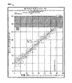
[0045]上述したように、単一の回転中に複数のスペクトルを得ることができる。終了点を決定する1つの方法において、ライブラリー内のインデックス数字に対して各スペクトルがマッチングされる。次いで、各スペクトルは、強力な線適合に対して使用される。線は、研磨の割合に対応する。図6を参照すれば、グラフ600は、ライブラリー内の回転インデックスに合致し且つ時間に基づいてプロットされた20個のスペクトルを示す。スペクトルの各々が異なるインデックスでマッチングするためにデータがある程度散在する。この散在は、ゾーン内の非均一厚み、ノイズ性のデータ、又はファクタの組み合わせによることもある。2つ以上のスペクトルが重畳する場合には、より大きな記号がグラフ600に描かれる。
[0045] As described above, multiple spectra can be obtained during a single rotation. In one method of determining the end point, each spectrum is matched against an index number in the library. Each spectrum is then used for strong line fitting. The line corresponds to the polishing rate. Referring to FIG. 6, a
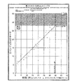
[0046]別の方法として、スペクトルが先ず平均化され、次いで、ライブラリーに対してマッチングされる。図7を参照すれば、全てのスペクトルが平均化され、その平均スペクトルを使用して、最良のインデックス突き合わせに対してライブラリーをサーチする。図6について述べた技術に使用されたものと同じ生のスペクトルを使用して、異なる、強力な線適合結果が得られる。これは、異なる終了点決定を生じさせる。 [0046] Alternatively, the spectra are first averaged and then matched against the library. Referring to FIG. 7, all spectra are averaged and the average spectrum is used to search the library for the best index match. Using the same raw spectrum as used in the technique described with respect to FIG. 6, different and strong line fitting results are obtained. This results in a different end point determination.
[0047]本明細書で説明される要旨及び機能的動作の実施形態は、本明細書で説明される構造及びその構造的等効物を含めて、デジタル電子回路、或いはコンピュータソフトウェア、ファームウェア、又はハードウェアで具現化することができ、或いはそれらの1つ以上の組み合わせで具現化することができる。本明細書に説明された要旨の実施形態は、1つ以上のコンピュータプログラム製品として具現化することができ、即ちデータ処理装置により実行するために又はデータ処理装置の動作を制御するために有形のプログラムキャリアにおいてエンコードされたコンピュータプログラムインストラクションの1つ以上のモジュールとして具現化することができる。有形のプログラムキャリアは、伝播信号又はコンピュータ読み取り可能な媒体である。伝播信号は、人為的に発生される信号、例えば、マシン発生される電気、光学又は電磁信号であり、これは、適当な受信装置へ送信してコンピュータにより実行するように情報をエンコードするために発生される。また、コンピュータ読み取り可能な媒体は、マシン読み取り可能な記憶装置、マシン読み取り可能な記憶基板、メモリ装置、マシン読み取り可能な伝播信号に作用する事柄の構成、或いはそれらの1つ以上の組み合わせである。 [0047] Embodiments of the subject matter and functional operations described herein may include digital electronic circuits or computer software, firmware, or structures including the structures described herein and structural equivalents thereof. It can be embodied in hardware or can be embodied in one or more combinations thereof. Embodiments of the subject matter described herein can be embodied as one or more computer program products, ie, tangible for execution by a data processing device or for controlling the operation of a data processing device. It can be embodied as one or more modules of computer program instructions encoded in a program carrier. A tangible program carrier is a propagated signal or a computer readable medium. A propagated signal is an artificially generated signal, eg, a machine generated electrical, optical or electromagnetic signal, that is transmitted to an appropriate receiving device to encode information for execution by a computer. Generated. Also, the computer readable medium may be a machine readable storage device, a machine readable storage substrate, a memory device, a configuration that affects machine readable propagation signals, or a combination of one or more thereof.
[0048]「データ処理装置」という語は、例えば、プログラム可能なプロセッサ、コンピュータ、或いはマルチプロセッサ又はコンピュータを含めて、データを処理するための全ての装置、デバイス及びマシンを包含する。装置は、ハードウェアに加えて、当該コンピュータプログラムのための実行環境を生成するコード、例えば、プロセッサファームウェア、プロトコルスタック、データベースマネージメントシステム、オペレーティングシステム、又はその1つ以上の組み合わせを構成するコードを包含することができる。 [0048] The term "data processing device" encompasses all devices, devices, and machines for processing data, including, for example, a programmable processor, computer, or multiprocessor or computer. In addition to hardware, the apparatus includes code that generates an execution environment for the computer program, eg, code that forms a processor firmware, protocol stack, database management system, operating system, or one or more combinations thereof. can do.
[0049]コンピュータプログラム(プログラム、ソフトウェア、ソフトウェアアプリケーション、スクリプト又はコードとしても知られている)は、コンパイル又は解釈言語、或いは宣言又は手続言語を含めて、任意の形式のプログラミング言語で書くことができ、更に、コンピューティング環境で使用するのに適したコンポーネント、サブルーチン又は他のユニットをスタンドアローンプログラム又はモジュールとして含む任意の形態で展開することができる。コンピュータプログラムは、必ずしも、ファイルシステム内のファイルに対応しない。プログラムは、他のプログラム又はデータ(例えば、マークアップ言語ドキュメントに記憶された1つ以上のスクリプト)を保持するファイルの一部分、当該プログラムに専用とされた単一のファイル、又は複数の座標付きファイル(例えば、1つ以上のモジュール、サブプログラム、又はコードの部分)に記憶することができる。コンピュータプログラムは、1つのサイトに配置されるか又は複数のサイトにわたって分散されて通信ネットワークによって相互接続される1つのコンピュータ又は複数のコンピュータにおいて実行されるように展開することができる。 [0049] A computer program (also known as a program, software, software application, script or code) can be written in any form of programming language, including a compiled or interpreted language, or a declaration or procedural language In addition, any form including components, subroutines or other units suitable for use in a computing environment may be deployed as a stand-alone program or module. A computer program does not necessarily correspond to a file in a file system. A program is a portion of a file that holds other programs or data (eg, one or more scripts stored in a markup language document), a single file dedicated to the program, or a plurality of coordinated files (Eg, one or more modules, subprograms, or portions of code). A computer program can be deployed to be executed on one computer or on multiple computers located at one site or distributed across multiple sites and interconnected by a communication network.
[0050]本明細書で述べるプロセス及びロジックフローは、入力データに対して動作して出力を発生することで機能を遂行するように1つ以上のコンピュータプログラムを実行する1つ以上のプログラム可能なプロセッサにより遂行することができる。また、このプロセス及びロジックフローは、特殊目的のロジック回路、例えば、FPGA(現場でプログラム可能なゲートアレイ)又はASIC(特定用途向け集積回路)によって遂行することもできるし、また、装置は、その特殊目的のロジック回路として具現化することもできる。 [0050] The processes and logic flows described herein are one or more programmable that execute one or more computer programs to perform functions by operating on input data and generating output. It can be performed by a processor. This process and logic flow can also be performed by special purpose logic circuits such as FPGAs (field programmable gate arrays) or ASICs (application specific integrated circuits), It can also be embodied as a special purpose logic circuit.
[0051]コンピュータプログラムを実行するのに適したプロセッサは、例えば、汎用及び特殊目的の両マイクロプロセッサ、並びに任意の種類のデジタルコンピュータの1つ以上のプロセッサを含む。一般的に、プロセッサは、リードオンリメモリ又はランダムアクセスメモリ或いはその両方からインストラクション及びデータを受け取る。コンピュータの本質的な要素は、インストラクションを遂行するためのプロセッサと、インストラクション及びデータを記憶するための1つ以上のメモリ装置である。また、一般的に、コンピュータは、データを記憶するための1つ以上の大量記憶装置、例えば、磁気ディスク、磁気光学ディスク又は光学ディスクも備え、或いはそこからデータを受け取り、そこへデータを転送し、又はその両方を行うよう作動的に結合される。しかしながら、コンピュータは、このような装置を有する必要はない。 [0051] Processors suitable for executing computer programs include, for example, both general and special purpose microprocessors, and one or more processors of any type of digital computer. Generally, a processor will receive instructions and data from a read-only memory or a random access memory or both. The essential elements of a computer are a processor for performing instructions and one or more memory devices for storing instructions and data. In general, a computer also includes one or more mass storage devices for storing data, such as a magnetic disk, a magneto-optical disk, or an optical disk, or receives data therefrom and transfers data thereto. , Or both. However, the computer need not have such a device.
[0052]コンピュータプログラムインストラクション及びデータを記憶するのに適したコンピュータ読み取り可能な媒体は、一例として、半導体メモリ装置、例えば、EPROM、EEPROM及びフラッシュメモリ装置;磁気ディスク、例えば、内部ハードディスク又は除去可能なディスク;磁気光学ディスク;並びにCD ROM及びDVD−ROMディスクを含めて、不揮発性メモリ、媒体及びメモリ装置の全ての形態を含む。プロセッサ及びメモリは、特殊目的のロジック回路により補足することができ、又はそれに合体することができる。 [0052] Computer readable media suitable for storing computer program instructions and data include, by way of example, semiconductor memory devices such as EPROM, EEPROM, and flash memory devices; magnetic disks such as internal hard disks or removable. Includes all forms of non-volatile memory, media and memory devices, including disks; magneto-optic disks; and CD ROM and DVD-ROM disks. The processor and the memory can be supplemented by, or incorporated in, special purpose logic circuitry.
[0053]ユーザとの対話を与えるために、本明細書に述べる要旨の実施形態は、ユーザに情報を表示するためのディスプレイ装置、例えば、CRT(陰極線管)又はLCD(液晶ディスプレイ)モニタと、ユーザがコンピュータへ入力を与えることができるようにするキーボード及びポインティング装置、例えば、マウス又はトラックボールとを有するコンピュータにおいて具現化することができる。ユーザとの対話を与えるのに他の種類の装置を使用することもでき、例えば、ユーザに与えられるフィードバックは、任意の形態の感覚フィードバック、例えば、視覚フィードバック、聴覚フィードバック又は触覚フィードバックであり、また、ユーザからの入力は、音響、スピーチ又は触覚入力を含む任意の形態で受け取ることができる。 [0053] In order to provide user interaction, the embodiments described herein include a display device for displaying information to a user, such as a CRT (cathode ray tube) or LCD (liquid crystal display) monitor; It can be embodied in a computer having a keyboard and pointing device, such as a mouse or trackball, that allows the user to provide input to the computer. Other types of devices can also be used to provide user interaction, for example, the feedback provided to the user is any form of sensory feedback, e.g. visual feedback, audio feedback or tactile feedback, and The input from the user can be received in any form including acoustic, speech or haptic input.
[0054]本明細書は、多数の細目を含んでいるが、それらは、発明の範囲又は特許請求の範囲を限定するものと解釈されてはならず、むしろ、特定の発明の特定の実施形態特有の特徴を説明するものと解釈されたい。また、別々の実施形態に関して本明細書に述べた幾つかの特徴は、単一の実施形態において組み合わせて具現化することもできる。逆に、単一の実施形態に関して説明した種々の特徴は、複数の実施形態において別々に又は適した副組合せ(subcombination)で具現化することもできる。更に、それらの特徴は、幾つかの組み合わせにおいて作用するものとして説明され且つそのように最初に請求もされるが、請求された組み合わせからの1つ以上の特徴を、あるケースでは、その組み合わせから削除することができ、且つ請求された組み合わせが副組み合わせ又は副組み合わせの変形へと向けられてもよい。 [0054] While this specification includes a number of details, they should not be construed to limit the scope of the invention or the claims, but rather specific embodiments of a particular invention. It should be construed as explaining the unique features. Certain features that are described in this specification in the context of separate embodiments can also be implemented in combination in a single embodiment. Conversely, various features described with respect to a single embodiment can also be embodied in multiple embodiments separately or in suitable subcombination. Further, although those features are described as acting in several combinations and initially claimed as such, one or more features from the claimed combination may in some cases be derived from the combination. It can be deleted and the claimed combination may be directed to sub-combinations or variations of sub-combinations.
[0055]同様に、動作は添付図面において特定の順序で描かれたが、これは、このような動作を、図示された特定の順序又は逐次の順序で遂行すること、又は希望の結果を得るために図示された全ての動作を遂行すること、を要求していると理解されてはならない。ある環境では、マルチタスク及び並列処理が効果的なことがある。更に、上述した実施形態において種々のシステムコンポーネントを分離したことは、全ての実施形態においてそのような分離を要求していると理解されてはならず、また、上述したプログラムコンポーネント及びシステムは、一般的に、単一のソフトウェア製品に一緒に一体化もできるし、又は複数のソフトウェア製品へとパッケージもできることを理解されたい。 [0055] Similarly, operations are depicted in a particular order in the accompanying drawings, which may be performed in a particular or sequential order as illustrated, or to obtain desired results. Therefore, it should not be understood that it is required to perform all the operations shown in the figure. In some environments, multitasking and parallel processing may be effective. Furthermore, the separation of various system components in the above-described embodiments should not be understood as requiring such separation in all embodiments, and the program components and systems described above are generally In particular, it should be understood that it can be integrated together into a single software product or packaged into multiple software products.
[0056]本明細書に述べる要旨の特定の実施形態を説明した。他の実施形態も、特許請求の範囲内に含まれる。例えば、特許請求の範囲に列挙された動作は、異なる順序で遂行されても、希望の結果を得ることができる。一例として、添付図面に描かれたプロセスは、希望の結果を得るのに、必ずしも、図示された特定の順序又は逐次の順序を必要としない。ある具現化においては、マルチタスク及び並列処理が効果的なこともある。 [0056] Specific embodiments of the subject matter described in this specification have been described. Other embodiments are within the scope of the claims. For example, the actions recited in the claims can be performed in a different order to achieve a desired result. By way of example, the processes depicted in the accompanying drawings do not necessarily require the particular order or sequential order shown to achieve the desired result. In some implementations, multitasking and parallel processing may be effective.
10…基板、20…研磨装置、22…駆動シャフト、24…プラテン、25…軸、26…くぼみ、30…研磨パッド、36…光学的アクセス部、38…研磨液体、39…アーム、50…その場の監視モジュール、51…光源、52…光検出器、53…光学的ヘッド、54…二股の光学的ケーブル、55…幹線、56、58…支線、70…キャリアヘッド、71…軸、72…支持構造体、74…キャリア駆動シャフト、76…キャリアヘッド回転モータ
DESCRIPTION OF
Claims (6)
基板を横切る経路にその場の監視モジュールを運ぶプラテンの回転中に第1スペクトルを得るステップと、
上記第1スペクトルをライブラリー内の複数のスペクトルと比較して、第1の合致するスペクトルを決定するステップであって、上記ライブラリー内の各スペクトルは、上記スペクトルが現れることが予想されるプラテン回転を表すインデックス数字と関連し、上記第1スペクトルの比較は、上記第1の合致するスペクトルに対する第1インデックス数字を決定する段階を含み、上記第1インデックス数字がNである、ステップと、
上記プラテンの、その後の回転中に第2スペクトルを得るステップであって、上記その後の回転は上記回転後のX回転であるステップと、
上記第2スペクトルを上記ライブラリー内の複数のスペクトルのうちのサブセットと比較して、第2の合致するスペクトルを決定するステップであって、上記第2スペクトルの比較は、上記第2の合致するスペクトルに対する第2インデックス数字を決定する段階を含み、自由度Yが所定の数字であり、且つ上記ライブラリー内の複数のスペクトルのサブセットは、(N+X)±Yのインデックス数字に対応するスペクトルであるステップと、
を備えた方法。 In the method of determining the polishing end point,
Obtaining a first spectrum during rotation of a platen carrying an in-situ monitoring module in a path across the substrate;
Comparing the first spectrum with a plurality of spectra in a library to determine a first matching spectrum , wherein each spectrum in the library is a platen on which the spectrum is expected to appear. In connection with an index number representing rotation, the comparison of the first spectrum includes determining a first index number for the first matching spectrum, wherein the first index number is N;
Obtaining a second spectrum during subsequent rotation of the platen , wherein the subsequent rotation is an X rotation after the rotation;
Comparing the second spectrum to a subset of a plurality of spectra in the library to determine a second matching spectrum, wherein the comparison of the second spectrum is the second matching spectrum; Determining a second index number for the spectrum, wherein the degree of freedom Y is a predetermined number, and a subset of the plurality of spectra in the library is a spectrum corresponding to an index number of (N + X) ± Y. Steps,
With a method.
研磨面を支持するための回転可能なプラテンと、
上記プラテン内の光源及び上記プラテン内の光検出器を含むその場の監視モジュールと、
上記研磨面に対して基板を保持すると共に上記基板を移動するように構成されるキャリアヘッドであって、上記光源からの光が上記基板の上記表面に向けられ且つ上記基板から反射した光が上記光検出器によって検出される、上記キャリアヘッドと、
上記キャリアヘッドを制御するためのコントローラと、
上記光検出器からの信号を受け取るように構成されたコンピュータであって、上記基板を横切る経路に上記その場の監視モジュールを運ぶプラテンの回転中に第1スペクトルを得て、この第1スペクトルをライブラリー内の複数のスペクトルと比較して、第1の合致するスペクトルを決定し、基板のその後の回転中に第2スペクトルを得て、この第2スペクトルをライブラリー内の複数のスペクトルのうちのサブセットと比較して、第2の合致するスペクトルを決定し、上記第1の合致するスペクトルに対する第1インデックス数字を決定し、上記第2の合致するスペクトルに対する第2インデックス数字を決定し、上記ライブラリー内の各スペクトルは、上記スペクトルが現れることが予想されるプラテン回転を表すインデックス数字と関連し、上記第1インデックス数字はNであり、上記その後の回転は上記回転後のX回転であり、自由度Yが所定の数字であり、且つ上記ライブラリー内の複数のスペクトルのサブセットは、(N+X)±Yのインデックス数字に合致するスペクトルである、ように構成された、上記コンピュータと、
を備えたシステム。 In a system for chemical mechanical polishing,
A rotatable platen to support the polishing surface;
A monitoring module situ, including an optical detector of the light source and within the platen in the platen,
A carrier head configured to hold the substrate relative to the polishing surface and move the substrate, wherein light from the light source is directed to the surface of the substrate and reflected from the substrate The carrier head detected by a photodetector;
A controller for controlling the carrier head;
A computer configured to receive a signal from the optical detector to obtain a first spectrum during the rotation of the platen carrying the monitoring module situ path across the substrate, the first spectrum Compared with a plurality of spectra in the library, a first matching spectrum is determined, a second spectrum is obtained during subsequent rotation of the substrate, and the second spectrum is extracted from the plurality of spectra in the library. compared to a subset of, and determine the second matching spectra to determine the first index number for the first matching spectra, to determine the second index numbers with respect to the second matching spectra, the Each spectrum in the library is associated with an index number that represents the platen rotation at which the spectrum is expected to appear. And, the first index number is N, the subsequent rotation is X rotation after the rotation, the degree of freedom Y is a predetermined number, and the plurality of subsets of spectra within the library ( N + X) The computer, configured to be a spectrum that matches the index number of ± Y;
With system.
上記第1スペクトルをライブラリー内の複数のスペクトルと比較して、第1の合致するスペクトルを決定し、上記ライブラリー内の各スペクトルは、上記スペクトルが現れることが予想されるプラテン回転を表すインデックス数字と関連し、
基板のその後の回転中に第2スペクトルを得て、
上記第2スペクトルを上記ライブラリー内の複数のスペクトルのうちのサブセットと比較して、第2の合致するスペクトルを決定し、
上記第1の合致するスペクトルに対する第1インデックス数字(この第1のインデックス数字はN)を決定し、且つ上記その後の回転は上記回転後のX回転であり、
上記第2の合致するスペクトルに対する第2インデックス数字を決定し、自由度Yが所定の数字であり、且つ上記ライブラリー内の複数のスペクトルのサブセットは、(N+X)±Yのインデックス数字に合致するスペクトルである、
ことを含むオペレーションをデータ処理装置に遂行させるように動作可能である、有形プログラムキャリアにエンコードされたコンピュータプログラム製品。 Obtaining the first spectrum during rotation of the platen carrying the in-situ monitoring module in a path across the substrate,
The first spectrum is compared with a plurality of spectra in the library to determine a first matching spectrum , each spectrum in the library being an index representing a platen rotation at which the spectrum is expected to appear. Associated with numbers,
During the subsequent rotation of the substrate to obtain a second spectrum,
Comparing the second spectrum to a subset of a plurality of spectra in the library to determine a second matching spectrum;
Determining a first index number (the first index number is N) for the first matching spectrum, and the subsequent rotation is an X rotation after the rotation;
A second index number for the second matching spectrum is determined, the degree of freedom Y is a predetermined number, and a subset of the plurality of spectra in the library matches an index number of (N + X) ± Y Spectrum,
A computer program product encoded on a tangible program carrier, operable to cause a data processing device to perform an operation comprising:
基板を横切る光学的監視モジュールの走査中に研磨を経験する上記基板から測定されたスペクトルを得るステップと、Obtaining a measured spectrum from the substrate experiencing polishing during scanning of the optical monitoring module across the substrate;
上記基板を横切る上記光学的監視モジュールの上記走査が遂行されるプラテン回転の数字Nを決定するステップと、Determining a platen rotation number N at which the scanning of the optical monitoring module across the substrate is performed;
上記スペクトルをライブラリー内の複数の基準スペクトルのうちのサブセットと比較して、上記サブセットから最も合致するスペクトルを決定するステップであって、上記サブセットは上記ライブラリー内の全ての基準スペクトルより少ない、少なくとも2つのスペクトルを含み、上記ライブラリー内の上記複数の基準スペクトルの各基準スペクトルは、上記基準スペクトルが現れることが予想されるプラテン回転を表すインデックス数字を有し、自由度Yが所定の数字であり、且つ上記ライブラリー内の上記複数の基準スペクトルの上記サブセットは、N±Y以内のインデックス数字を有する基準スペクトルであるステップと、Comparing the spectrum to a subset of a plurality of reference spectra in a library to determine a best-matching spectrum from the subset, the subset being less than all reference spectra in the library; Each of the plurality of reference spectra in the library includes at least two spectra, each reference spectrum having an index number representing a platen rotation in which the reference spectrum is expected to appear, and a degree of freedom Y is a predetermined number And the subset of the plurality of reference spectra in the library is a reference spectrum having an index number within N ± Y;
前記最も合致するスペクトルに対するインデックス数字を決定するステップと、Determining an index number for the best matching spectrum;
を備えた方法。With a method.
研磨面を支持するための回転可能なプラテンと、A rotatable platen to support the polishing surface;
上記プラテン内の光源と、A light source in the platen;
上記プラテン内の光検出器と、A photodetector in the platen;
上記研磨面に対して基板を保持すると共に上記基板を移動するように構成されるキャリアヘッドであって、上記光源からの光が上記基板の上記表面に向けられ且つ上記基板から反射した光が上記光検出器によって検出される、上記キャリアヘッドと、A carrier head configured to hold the substrate relative to the polishing surface and move the substrate, wherein light from the light source is directed to the surface of the substrate and reflected from the substrate The carrier head detected by a photodetector;
上記キャリアヘッドを制御するためのコントローラと、A controller for controlling the carrier head;
上記光検出器からの信号を受け取るように構成されたコンピュータであって、上記基板を横切る光学的監視モジュールの走査が遂行されるプラテン回転の数字Nを決定し、上記スペクトルをライブラリー内の複数の基準スペクトルのうちのサブセットと比較して、上記サブセットから最も合致するスペクトルを決定し、上記ライブラリー内の上記複数の基準スペクトルの各基準スペクトルのうちの前記最も合致するスペクトルに対するインデックス数字を決定し、上記サブセットは上記ライブラリー内の全ての基準スペクトルより少ない、少なくとも2つのスペクトルを含み、上記ライブラリー内の上記複数の基準スペクトルの各基準スペクトルは、上記基準スペクトルが現れることが予想されるプラテン回転を表すインデックス数字を有し、自由度Yが所定の数字であり、且つ上記ライブラリー内の上記複数の基準スペクトルの上記サブセットは、N±Y以内のインデックス数字を有する基準スペクトルである、ように構成された、上記コンピュータと、A computer configured to receive a signal from the photodetector, determining a number N of platen rotations in which scanning of the optical monitoring module across the substrate is performed, and storing the spectrum in a library Determine the best-matching spectrum from the subset compared to a subset of the reference spectra and determine an index number for the best-matching spectrum of each reference spectrum of the plurality of reference spectra in the library And the subset includes at least two spectra less than all the reference spectra in the library, and each reference spectrum of the plurality of reference spectra in the library is expected to exhibit the reference spectrum. Has index numbers representing platen rotation Freedom Y is a predetermined number, and said subset of said plurality of reference spectra within the library, a reference spectrum with index numbers within N ± Y, configured to, with the computer,
を備えたシステム。With system.
上記基板を横切る上記光学的監視モジュールの上記走査が遂行されるプラテン回転の数字Nを決定することと、Determining a platen rotation number N at which the scanning of the optical monitoring module across the substrate is performed;
上記スペクトルをライブラリー内の複数の基準スペクトルのうちのサブセットと比較して、上記サブセットから最も合致するスペクトルを決定することであって、上記サブセットは上記ライブラリー内の全ての基準スペクトルより少ない、少なくとも2つのスペクトルを含み、上記ライブラリー内の上記複数の基準スペクトルの各基準スペクトルは、上記基準スペクトルが現れることが予想されるプラテン回転を表すインデックス数字を有し、自由度Yが所定の数字であり、且つ上記ライブラリー内の上記複数の基準スペクトルの上記サブセットは、N±Y以内のインデックス数字を有する基準スペクトルであることと、Comparing the spectrum to a subset of a plurality of reference spectra in a library to determine a best-matching spectrum from the subset, wherein the subset is less than all reference spectra in the library; Each of the plurality of reference spectra in the library includes at least two spectra, each reference spectrum having an index number representing a platen rotation in which the reference spectrum is expected to appear, and a degree of freedom Y is a predetermined number And the subset of the plurality of reference spectra in the library is a reference spectrum having an index number within N ± Y;
前記最も合致するスペクトルに対するインデックス数字を決定することと、Determining an index number for the best matching spectrum;
を含むオペレーションをデータ処理装置に遂行させるように動作可能である、有形プログラムキャリアにエンコードされたコンピュータプログラム製品。A computer program product encoded on a tangible program carrier, operable to cause a data processing device to perform an operation comprising:
Applications Claiming Priority (2)
| Application Number | Priority Date | Filing Date | Title |
|---|---|---|---|
| US89148707P | 2007-02-23 | 2007-02-23 | |
| US60/891,487 | 2007-02-23 |
Related Parent Applications (1)
| Application Number | Title | Priority Date | Filing Date |
|---|---|---|---|
| JP2009551052A Division JP5654753B2 (en) | 2007-02-23 | 2008-02-22 | Determination of polishing end point using spectrum |
Publications (2)
| Publication Number | Publication Date |
|---|---|
| JP2013232660A JP2013232660A (en) | 2013-11-14 |
| JP5774059B2 true JP5774059B2 (en) | 2015-09-02 |
Family
ID=39710785
Family Applications (2)
| Application Number | Title | Priority Date | Filing Date |
|---|---|---|---|
| JP2009551052A Active JP5654753B2 (en) | 2007-02-23 | 2008-02-22 | Determination of polishing end point using spectrum |
| JP2013127106A Active JP5774059B2 (en) | 2007-02-23 | 2013-06-18 | Determination of polishing end point using spectrum |
Family Applications Before (1)
| Application Number | Title | Priority Date | Filing Date |
|---|---|---|---|
| JP2009551052A Active JP5654753B2 (en) | 2007-02-23 | 2008-02-22 | Determination of polishing end point using spectrum |
Country Status (6)
| Country | Link |
|---|---|
| US (2) | US8569174B2 (en) |
| EP (1) | EP2125291A4 (en) |
| JP (2) | JP5654753B2 (en) |
| KR (3) | KR101504508B1 (en) |
| TW (1) | TWI445098B (en) |
| WO (1) | WO2008103964A2 (en) |
Families Citing this family (46)
| Publication number | Priority date | Publication date | Assignee | Title |
|---|---|---|---|---|
| US8260446B2 (en) | 2005-08-22 | 2012-09-04 | Applied Materials, Inc. | Spectrographic monitoring of a substrate during processing using index values |
| US8392012B2 (en) * | 2008-10-27 | 2013-03-05 | Applied Materials, Inc. | Multiple libraries for spectrographic monitoring of zones of a substrate during processing |
| US7998358B2 (en) | 2006-10-31 | 2011-08-16 | Applied Materials, Inc. | Peak-based endpointing for chemical mechanical polishing |
| KR101504508B1 (en) | 2007-02-23 | 2015-03-20 | 어플라이드 머티어리얼스, 인코포레이티드 | Use of spectra to determine polishing end points |
| US20090275265A1 (en) * | 2008-05-02 | 2009-11-05 | Applied Materials, Inc. | Endpoint detection in chemical mechanical polishing using multiple spectra |
| US8369978B2 (en) * | 2008-09-04 | 2013-02-05 | Applied Materials | Adjusting polishing rates by using spectrographic monitoring of a substrate during processing |
| WO2010062497A2 (en) * | 2008-10-27 | 2010-06-03 | Applied Materials, Inc. | Goodness of fit in spectrographic monitoring of a substrate during processing |
| US20100103422A1 (en) * | 2008-10-27 | 2010-04-29 | Applied Materials, Inc. | Goodness of fit in spectrographic monitoring of a substrate during processing |
| US8628376B2 (en) * | 2008-11-07 | 2014-01-14 | Applied Materials, Inc. | In-line wafer thickness sensing |
| US8352061B2 (en) | 2008-11-14 | 2013-01-08 | Applied Materials, Inc. | Semi-quantitative thickness determination |
| US8039397B2 (en) * | 2008-11-26 | 2011-10-18 | Applied Materials, Inc. | Using optical metrology for within wafer feed forward process control |
| JP5968783B2 (en) * | 2009-11-03 | 2016-08-10 | アプライド マテリアルズ インコーポレイテッドApplied Materials,Incorporated | End point method using the relationship between peak position and time in spectral contour plots |
| JP5728239B2 (en) * | 2010-03-02 | 2015-06-03 | 株式会社荏原製作所 | Polishing monitoring method, polishing method, polishing monitoring apparatus, and polishing apparatus |
| US9579767B2 (en) | 2010-04-28 | 2017-02-28 | Applied Materials, Inc. | Automatic generation of reference spectra for optical monitoring of substrates |
| TWI496661B (en) * | 2010-04-28 | 2015-08-21 | 應用材料股份有限公司 | Automatic generation of reference spectra for optical monitoring |
| CN106252220B (en) * | 2010-05-05 | 2019-06-11 | 应用材料公司 | Dynamic or adaptive tracking of spectral signatures for endpoint detection |
| US8190285B2 (en) * | 2010-05-17 | 2012-05-29 | Applied Materials, Inc. | Feedback for polishing rate correction in chemical mechanical polishing |
| US8666665B2 (en) * | 2010-06-07 | 2014-03-04 | Applied Materials, Inc. | Automatic initiation of reference spectra library generation for optical monitoring |
| JP2012019114A (en) * | 2010-07-08 | 2012-01-26 | Tokyo Seimitsu Co Ltd | Polishing end point detection system and polishing end point detection method |
| JP5612945B2 (en) | 2010-07-23 | 2014-10-22 | 株式会社荏原製作所 | Method and apparatus for monitoring progress of substrate polishing |
| TWI521625B (en) * | 2010-07-30 | 2016-02-11 | 應用材料股份有限公司 | Use spectral monitoring to detect level removal |
| US8954186B2 (en) | 2010-07-30 | 2015-02-10 | Applied Materials, Inc. | Selecting reference libraries for monitoring of multiple zones on a substrate |
| WO2012054263A2 (en) * | 2010-10-20 | 2012-04-26 | Applied Materials, Inc. | Multiple matching reference spectra for in-situ optical monitoring |
| US8547538B2 (en) * | 2011-04-21 | 2013-10-01 | Applied Materials, Inc. | Construction of reference spectra with variations in environmental effects |
| US8755928B2 (en) * | 2011-04-27 | 2014-06-17 | Applied Materials, Inc. | Automatic selection of reference spectra library |
| US8942842B2 (en) | 2011-04-28 | 2015-01-27 | Applied Materials, Inc. | Varying optical coefficients to generate spectra for polishing control |
| WO2013133974A1 (en) | 2012-03-08 | 2013-09-12 | Applied Materials, Inc. | Fitting of optical model to measured spectrum |
| US9248544B2 (en) * | 2012-07-18 | 2016-02-02 | Applied Materials, Inc. | Endpoint detection during polishing using integrated differential intensity |
| US9221147B2 (en) * | 2012-10-23 | 2015-12-29 | Applied Materials, Inc. | Endpointing with selective spectral monitoring |
| US20140141696A1 (en) * | 2012-11-21 | 2014-05-22 | Applied Materials, Inc. | Polishing System with In-Sequence Sensor |
| US20140242881A1 (en) * | 2013-02-27 | 2014-08-28 | Applied Materials, Inc. | Feed forward parameter values for use in theoretically generating spectra |
| JP6195754B2 (en) * | 2013-07-19 | 2017-09-13 | 株式会社荏原製作所 | Polishing apparatus and polishing state monitoring method |
| TWI635929B (en) | 2013-07-11 | 2018-09-21 | 日商荏原製作所股份有限公司 | Polishing apparatus and polished-state monitoring method |
| US10502694B2 (en) | 2013-08-06 | 2019-12-10 | Kla-Tencor Corporation | Methods and apparatus for patterned wafer characterization |
| WO2015163164A1 (en) * | 2014-04-22 | 2015-10-29 | 株式会社 荏原製作所 | Polishing method and polishing apparatus |
| US20160013085A1 (en) * | 2014-07-10 | 2016-01-14 | Applied Materials, Inc. | In-Situ Acoustic Monitoring of Chemical Mechanical Polishing |
| US20160033958A1 (en) * | 2014-08-01 | 2016-02-04 | Globalfoundries Inc. | Endpoint determination using individually measured target spectra |
| TWI789385B (en) * | 2017-04-21 | 2023-01-11 | 美商應用材料股份有限公司 | Polishing apparatus using neural network for monitoring |
| JP6902452B2 (en) * | 2017-10-19 | 2021-07-14 | 株式会社荏原製作所 | Polishing equipment |
| TWI825075B (en) | 2018-04-03 | 2023-12-11 | 美商應用材料股份有限公司 | Polishing apparatus, polishing system, method, and computer storage medium using machine learning and compensation for pad thickness |
| CN111886686B (en) | 2018-09-26 | 2024-08-02 | 应用材料公司 | Compensation of substrate doping in edge reconstruction for in-situ electromagnetic induction monitoring |
| JP7086835B2 (en) * | 2018-12-28 | 2022-06-20 | 株式会社荏原製作所 | Polishing recipe determination device |
| CN110181984A (en) * | 2019-06-03 | 2019-08-30 | 泉州龙捷园林古建工程有限公司 | A method of in production picture and text on plate |
| US11282755B2 (en) * | 2019-08-27 | 2022-03-22 | Applied Materials, Inc. | Asymmetry correction via oriented wafer loading |
| CN115038549B (en) | 2020-06-24 | 2024-03-12 | 应用材料公司 | Determination of substrate layer thickness using polishing pad wear compensation |
| WO2023249678A1 (en) * | 2022-06-22 | 2023-12-28 | Applied Materials, Inc. | Window logic for control of polishing process |
Family Cites Families (52)
| Publication number | Priority date | Publication date | Assignee | Title |
|---|---|---|---|---|
| US7004A (en) * | 1850-01-08 | Connecting ctjttees to shafts of boeing instetjments | ||
| US5893796A (en) | 1995-03-28 | 1999-04-13 | Applied Materials, Inc. | Forming a transparent window in a polishing pad for a chemical mechanical polishing apparatus |
| US5747380A (en) | 1996-02-26 | 1998-05-05 | Taiwan Semiconductor Manufacturing Company, Ltd. | Robust end-point detection for contact and via etching |
| US6489624B1 (en) * | 1997-07-18 | 2002-12-03 | Nikon Corporation | Apparatus and methods for detecting thickness of a patterned layer |
| US6271047B1 (en) | 1998-05-21 | 2001-08-07 | Nikon Corporation | Layer-thickness detection methods and apparatus for wafers and the like, and polishing apparatus comprising same |
| US6361646B1 (en) * | 1998-06-08 | 2002-03-26 | Speedfam-Ipec Corporation | Method and apparatus for endpoint detection for chemical mechanical polishing |
| TW398036B (en) | 1998-08-18 | 2000-07-11 | Promos Technologies Inc | Method of monitoring of chemical mechanical polishing end point and uniformity |
| IL125964A (en) * | 1998-08-27 | 2003-10-31 | Tevet Process Control Technolo | Method and apparatus for measuring the thickness of a transparent film, particularly of a photoresist film on a semiconductor substrate |
| US6159073A (en) * | 1998-11-02 | 2000-12-12 | Applied Materials, Inc. | Method and apparatus for measuring substrate layer thickness during chemical mechanical polishing |
| WO2000026613A1 (en) | 1998-11-02 | 2000-05-11 | Applied Materials, Inc. | Optical monitoring of radial ranges in chemical mechanical polishing a metal layer on a substrate |
| US6908374B2 (en) * | 1998-12-01 | 2005-06-21 | Nutool, Inc. | Chemical mechanical polishing endpoint detection |
| JP2000183001A (en) | 1998-12-10 | 2000-06-30 | Okamoto Machine Tool Works Ltd | Polish end-point detecting method for wafer and chemical-mechanical polishing device used for the same |
| US6204922B1 (en) | 1998-12-11 | 2001-03-20 | Filmetrics, Inc. | Rapid and accurate thin film measurement of individual layers in a multi-layered or patterned sample |
| US6172756B1 (en) | 1998-12-11 | 2001-01-09 | Filmetrics, Inc. | Rapid and accurate end point detection in a noisy environment |
| US6184985B1 (en) | 1998-12-11 | 2001-02-06 | Filmetrics, Inc. | Spectrometer configured to provide simultaneous multiple intensity spectra from independent light sources |
| US6190234B1 (en) | 1999-01-25 | 2001-02-20 | Applied Materials, Inc. | Endpoint detection with light beams of different wavelengths |
| JP2000310512A (en) | 1999-04-28 | 2000-11-07 | Hitachi Ltd | Method and apparatus for measuring thin film thickness and method and apparatus for manufacturing thin film device using the same |
| JP3327289B2 (en) | 2000-03-29 | 2002-09-24 | 株式会社ニコン | Process end point measuring device, measuring method, polishing device, semiconductor device manufacturing method, and recording medium recording signal processing program |
| US6358327B1 (en) | 1999-06-29 | 2002-03-19 | Applied Materials, Inc. | Method for endpoint detection using throttle valve position |
| US6340602B1 (en) * | 1999-12-10 | 2002-01-22 | Sensys Instruments | Method of measuring meso-scale structures on wafers |
| US6399501B2 (en) * | 1999-12-13 | 2002-06-04 | Applied Materials, Inc. | Method and apparatus for detecting polishing endpoint with optical monitoring |
| JP3259225B2 (en) | 1999-12-27 | 2002-02-25 | 株式会社ニコン | Polishing status monitoring method and apparatus, polishing apparatus, process wafer, semiconductor device manufacturing method, and semiconductor device |
| JP2001287159A (en) | 2000-04-05 | 2001-10-16 | Nikon Corp | Surface condition measuring method, measuring apparatus, polishing apparatus, and semiconductor device manufacturing method |
| AU2001279247A1 (en) * | 2000-08-10 | 2002-02-25 | Sensys Instruments Corporation | Database interpolation method for optical measurement of diffractive microstructures |
| WO2002065545A2 (en) * | 2001-02-12 | 2002-08-22 | Sensys Instruments Corporation | Overlay alignment metrology using diffraction gratings |
| US6676482B2 (en) * | 2001-04-20 | 2004-01-13 | Speedfam-Ipec Corporation | Learning method and apparatus for predictive determination of endpoint during chemical mechanical planarization using sparse sampling |
| JP2002359217A (en) * | 2001-05-31 | 2002-12-13 | Omron Corp | Polishing end point detection method and apparatus |
| US6762838B2 (en) * | 2001-07-02 | 2004-07-13 | Tevet Process Control Technologies Ltd. | Method and apparatus for production line screening |
| JP3932836B2 (en) | 2001-07-27 | 2007-06-20 | 株式会社日立製作所 | Thin film thickness measuring method and apparatus, and device manufacturing method using the same |
| US6678046B2 (en) * | 2001-08-28 | 2004-01-13 | Therma-Wave, Inc. | Detector configurations for optical metrology |
| US6618130B2 (en) * | 2001-08-28 | 2003-09-09 | Speedfam-Ipec Corporation | Method and apparatus for optical endpoint detection during chemical mechanical polishing |
| US6898596B2 (en) * | 2001-10-23 | 2005-05-24 | Therma-Wave, Inc. | Evolution of library data sets |
| US6678055B2 (en) * | 2001-11-26 | 2004-01-13 | Tevet Process Control Technologies Ltd. | Method and apparatus for measuring stress in semiconductor wafers |
| JP4660091B2 (en) * | 2001-12-31 | 2011-03-30 | 東京エレクトロン株式会社 | Material processing system and method for characterizing material processing system |
| US6942546B2 (en) | 2002-01-17 | 2005-09-13 | Asm Nutool, Inc. | Endpoint detection for non-transparent polishing member |
| US6813034B2 (en) * | 2002-02-05 | 2004-11-02 | Therma-Wave, Inc. | Analysis of isolated and aperiodic structures with simultaneous multiple angle of incidence measurements |
| US6806948B2 (en) * | 2002-03-29 | 2004-10-19 | Lam Research Corporation | System and method of broad band optical end point detection for film change indication |
| US6947135B2 (en) * | 2002-07-01 | 2005-09-20 | Therma-Wave, Inc. | Reduced multicubic database interpolation method for optical measurement of diffractive microstructures |
| JP4542324B2 (en) | 2002-10-17 | 2010-09-15 | 株式会社荏原製作所 | Polishing state monitoring device and polishing device |
| US6885467B2 (en) * | 2002-10-28 | 2005-04-26 | Tevet Process Control Technologies Ltd. | Method and apparatus for thickness decomposition of complicated layer structures |
| US8257546B2 (en) | 2003-04-11 | 2012-09-04 | Applied Materials, Inc. | Method and system for monitoring an etch process |
| WO2004097723A1 (en) | 2003-04-29 | 2004-11-11 | Anoto Ip Lic Hb | Methods, apparatus, computer program and storage medium for position decoding |
| US7097537B1 (en) * | 2003-08-18 | 2006-08-29 | Applied Materials, Inc. | Determination of position of sensor measurements during polishing |
| JP4464642B2 (en) | 2003-09-10 | 2010-05-19 | 株式会社荏原製作所 | Polishing state monitoring apparatus, polishing state monitoring method, polishing apparatus, and polishing method |
| JP2005159203A (en) | 2003-11-28 | 2005-06-16 | Hitachi Ltd | Film thickness measuring method and apparatus, polishing rate calculating method, CMP processing method and apparatus |
| US7255771B2 (en) * | 2004-03-26 | 2007-08-14 | Applied Materials, Inc. | Multiple zone carrier head with flexible membrane |
| US7120553B2 (en) | 2004-07-22 | 2006-10-10 | Applied Materials, Inc. | Iso-reflectance wavelengths |
| US7406394B2 (en) | 2005-08-22 | 2008-07-29 | Applied Materials, Inc. | Spectra based endpointing for chemical mechanical polishing |
| KR101324644B1 (en) | 2005-08-22 | 2013-11-01 | 어플라이드 머티어리얼스, 인코포레이티드 | Apparatus and methods for spectrum based monitoring of chemical mechanical polishing |
| US7226339B2 (en) * | 2005-08-22 | 2007-06-05 | Applied Materials, Inc. | Spectrum based endpointing for chemical mechanical polishing |
| KR101398570B1 (en) * | 2005-08-22 | 2014-05-22 | 어플라이드 머티어리얼스, 인코포레이티드 | Apparatus and methods for spectrum based monitoring of chemical mechanical polishing |
| KR101504508B1 (en) | 2007-02-23 | 2015-03-20 | 어플라이드 머티어리얼스, 인코포레이티드 | Use of spectra to determine polishing end points |
-
2008
- 2008-02-22 KR KR1020097019664A patent/KR101504508B1/en active Active
- 2008-02-22 TW TW97106349A patent/TWI445098B/en active
- 2008-02-22 KR KR1020157033828A patent/KR101643992B1/en active Active
- 2008-02-22 US US12/036,174 patent/US8569174B2/en active Active
- 2008-02-22 EP EP08730580.1A patent/EP2125291A4/en not_active Withdrawn
- 2008-02-22 KR KR1020147032982A patent/KR101678082B1/en active Active
- 2008-02-22 JP JP2009551052A patent/JP5654753B2/en active Active
- 2008-02-22 WO PCT/US2008/054807 patent/WO2008103964A2/en not_active Ceased
-
2013
- 2013-06-18 JP JP2013127106A patent/JP5774059B2/en active Active
- 2013-09-30 US US14/041,113 patent/US9142466B2/en active Active
Also Published As
| Publication number | Publication date |
|---|---|
| EP2125291A2 (en) | 2009-12-02 |
| JP5654753B2 (en) | 2015-01-14 |
| TW200849416A (en) | 2008-12-16 |
| US20080206993A1 (en) | 2008-08-28 |
| KR101678082B1 (en) | 2016-11-21 |
| WO2008103964A2 (en) | 2008-08-28 |
| US8569174B2 (en) | 2013-10-29 |
| KR20090112765A (en) | 2009-10-28 |
| EP2125291A4 (en) | 2013-08-07 |
| WO2008103964A3 (en) | 2008-11-27 |
| JP2013232660A (en) | 2013-11-14 |
| JP2010519771A (en) | 2010-06-03 |
| KR20140147146A (en) | 2014-12-29 |
| KR20150140400A (en) | 2015-12-15 |
| TWI445098B (en) | 2014-07-11 |
| US20140045282A1 (en) | 2014-02-13 |
| KR101504508B1 (en) | 2015-03-20 |
| US9142466B2 (en) | 2015-09-22 |
| KR101643992B1 (en) | 2016-07-29 |
Similar Documents
| Publication | Publication Date | Title |
|---|---|---|
| JP5774059B2 (en) | Determination of polishing end point using spectrum | |
| JP5542802B2 (en) | Endpoint detection in chemical mechanical polishing using multiple spectra | |
| JP6316794B2 (en) | Dynamic or adaptive tracking of spectral features for endpoint detection | |
| JP5675617B2 (en) | Polishing speed adjustment using spectral monitoring of substrates during processing | |
| JP6017538B2 (en) | Construction of a reference spectrum with changes in environmental influences | |
| US8992286B2 (en) | Weighted regression of thickness maps from spectral data | |
| US9233450B2 (en) | Optical detection of metal layer clearance | |
| US20100114532A1 (en) | Weighted spectrographic monitoring of a substrate during processing | |
| KR20110102376A (en) | Use optical measurements for feed back and feed forward process control | |
| JP5774482B2 (en) | Goodness of fit in spectral monitoring of substrates during processing | |
| US9073169B2 (en) | Feedback control of polishing using optical detection of clearance | |
| JP6292819B2 (en) | Endpoint determination using selective spectral monitoring | |
| US9168630B2 (en) | User-input functions for data sequences in polishing endpoint detection | |
| US9811077B2 (en) | Polishing with pre deposition spectrum |
Legal Events
| Date | Code | Title | Description |
|---|---|---|---|
| A977 | Report on retrieval |
Free format text: JAPANESE INTERMEDIATE CODE: A971007 Effective date: 20140514 |
|
| A131 | Notification of reasons for refusal |
Free format text: JAPANESE INTERMEDIATE CODE: A131 Effective date: 20140603 |
|
| A601 | Written request for extension of time |
Free format text: JAPANESE INTERMEDIATE CODE: A601 Effective date: 20140829 |
|
| A602 | Written permission of extension of time |
Free format text: JAPANESE INTERMEDIATE CODE: A602 Effective date: 20140903 |
|
| A521 | Request for written amendment filed |
Free format text: JAPANESE INTERMEDIATE CODE: A523 Effective date: 20141003 |
|
| TRDD | Decision of grant or rejection written | ||
| A01 | Written decision to grant a patent or to grant a registration (utility model) |
Free format text: JAPANESE INTERMEDIATE CODE: A01 Effective date: 20150602 |
|
| A61 | First payment of annual fees (during grant procedure) |
Free format text: JAPANESE INTERMEDIATE CODE: A61 Effective date: 20150630 |
|
| R150 | Certificate of patent or registration of utility model |
Ref document number: 5774059 Country of ref document: JP Free format text: JAPANESE INTERMEDIATE CODE: R150 |
|
| R250 | Receipt of annual fees |
Free format text: JAPANESE INTERMEDIATE CODE: R250 |
|
| R250 | Receipt of annual fees |
Free format text: JAPANESE INTERMEDIATE CODE: R250 |
|
| R250 | Receipt of annual fees |
Free format text: JAPANESE INTERMEDIATE CODE: R250 |
|
| R250 | Receipt of annual fees |
Free format text: JAPANESE INTERMEDIATE CODE: R250 |
|
| R250 | Receipt of annual fees |
Free format text: JAPANESE INTERMEDIATE CODE: R250 |
|
| R250 | Receipt of annual fees |
Free format text: JAPANESE INTERMEDIATE CODE: R250 |
|
| R250 | Receipt of annual fees |
Free format text: JAPANESE INTERMEDIATE CODE: R250 |