KR20200048205A - Flexible circuit film and electronic device comprising the same - Google Patents
Flexible circuit film and electronic device comprising the same Download PDFInfo
- Publication number
- KR20200048205A KR20200048205A KR1020180130013A KR20180130013A KR20200048205A KR 20200048205 A KR20200048205 A KR 20200048205A KR 1020180130013 A KR1020180130013 A KR 1020180130013A KR 20180130013 A KR20180130013 A KR 20180130013A KR 20200048205 A KR20200048205 A KR 20200048205A
- Authority
- KR
- South Korea
- Prior art keywords
- film
- layer
- bending
- flexible circuit
- touch
- Prior art date
Links
- 238000005452 bending Methods 0.000 claims abstract description 165
- 238000000034 method Methods 0.000 claims abstract description 48
- 239000010410 layer Substances 0.000 claims description 257
- 239000000758 substrate Substances 0.000 claims description 45
- 230000017525 heat dissipation Effects 0.000 claims description 40
- 239000000463 material Substances 0.000 claims description 32
- 239000011247 coating layer Substances 0.000 claims description 31
- 229920001721 polyimide Polymers 0.000 claims description 16
- 239000004642 Polyimide Substances 0.000 claims description 15
- 238000005192 partition Methods 0.000 claims description 14
- 229910000679 solder Inorganic materials 0.000 claims description 4
- 230000008569 process Effects 0.000 abstract description 32
- 239000010408 film Substances 0.000 description 188
- 239000000853 adhesive Substances 0.000 description 27
- 230000001070 adhesive effect Effects 0.000 description 27
- RYGMFSIKBFXOCR-UHFFFAOYSA-N Copper Chemical compound [Cu] RYGMFSIKBFXOCR-UHFFFAOYSA-N 0.000 description 24
- 239000012790 adhesive layer Substances 0.000 description 21
- 239000011889 copper foil Substances 0.000 description 21
- 238000005538 encapsulation Methods 0.000 description 12
- 230000003287 optical effect Effects 0.000 description 9
- 238000006243 chemical reaction Methods 0.000 description 8
- 230000006870 function Effects 0.000 description 7
- 239000002184 metal Substances 0.000 description 7
- 229910052751 metal Inorganic materials 0.000 description 7
- 239000004820 Pressure-sensitive adhesive Substances 0.000 description 6
- 239000011521 glass Substances 0.000 description 6
- 239000010409 thin film Substances 0.000 description 6
- 229920003023 plastic Polymers 0.000 description 5
- 229920000139 polyethylene terephthalate Polymers 0.000 description 5
- 239000005020 polyethylene terephthalate Substances 0.000 description 5
- 238000003860 storage Methods 0.000 description 5
- 238000005516 engineering process Methods 0.000 description 4
- 238000002347 injection Methods 0.000 description 4
- 239000007924 injection Substances 0.000 description 4
- 239000011810 insulating material Substances 0.000 description 4
- 230000007935 neutral effect Effects 0.000 description 4
- 239000004033 plastic Substances 0.000 description 4
- 239000003351 stiffener Substances 0.000 description 4
- QVGXLLKOCUKJST-UHFFFAOYSA-N atomic oxygen Chemical compound [O] QVGXLLKOCUKJST-UHFFFAOYSA-N 0.000 description 3
- 230000004888 barrier function Effects 0.000 description 3
- 239000011248 coating agent Substances 0.000 description 3
- 238000000576 coating method Methods 0.000 description 3
- 229910052802 copper Inorganic materials 0.000 description 3
- 239000010949 copper Substances 0.000 description 3
- 230000007547 defect Effects 0.000 description 3
- 230000000694 effects Effects 0.000 description 3
- 239000006260 foam Substances 0.000 description 3
- 229910010272 inorganic material Inorganic materials 0.000 description 3
- 239000011147 inorganic material Substances 0.000 description 3
- 229910052760 oxygen Inorganic materials 0.000 description 3
- 239000001301 oxygen Substances 0.000 description 3
- 230000000149 penetrating effect Effects 0.000 description 3
- 239000004417 polycarbonate Substances 0.000 description 3
- 229920000515 polycarbonate Polymers 0.000 description 3
- 229920005989 resin Polymers 0.000 description 3
- 239000011347 resin Substances 0.000 description 3
- 229920012266 Poly(ether sulfone) PES Polymers 0.000 description 2
- 239000002131 composite material Substances 0.000 description 2
- 239000013039 cover film Substances 0.000 description 2
- 238000009795 derivation Methods 0.000 description 2
- 238000013461 design Methods 0.000 description 2
- 230000005611 electricity Effects 0.000 description 2
- 229920006332 epoxy adhesive Polymers 0.000 description 2
- 230000005525 hole transport Effects 0.000 description 2
- 239000007769 metal material Substances 0.000 description 2
- 238000012986 modification Methods 0.000 description 2
- 230000004048 modification Effects 0.000 description 2
- 239000011368 organic material Substances 0.000 description 2
- 229920003229 poly(methyl methacrylate) Polymers 0.000 description 2
- 229910021420 polycrystalline silicon Inorganic materials 0.000 description 2
- 239000002861 polymer material Substances 0.000 description 2
- 239000004926 polymethyl methacrylate Substances 0.000 description 2
- 239000011241 protective layer Substances 0.000 description 2
- 230000001846 repelling effect Effects 0.000 description 2
- 239000004065 semiconductor Substances 0.000 description 2
- 230000003068 static effect Effects 0.000 description 2
- 229920001187 thermosetting polymer Polymers 0.000 description 2
- 239000005341 toughened glass Substances 0.000 description 2
- OKTJSMMVPCPJKN-UHFFFAOYSA-N Carbon Chemical compound [C] OKTJSMMVPCPJKN-UHFFFAOYSA-N 0.000 description 1
- 239000004593 Epoxy Substances 0.000 description 1
- BQCADISMDOOEFD-UHFFFAOYSA-N Silver Chemical compound [Ag] BQCADISMDOOEFD-UHFFFAOYSA-N 0.000 description 1
- 230000002159 abnormal effect Effects 0.000 description 1
- 229910021417 amorphous silicon Inorganic materials 0.000 description 1
- 230000005540 biological transmission Effects 0.000 description 1
- 230000000903 blocking effect Effects 0.000 description 1
- 230000008859 change Effects 0.000 description 1
- 239000003086 colorant Substances 0.000 description 1
- 238000009500 colour coating Methods 0.000 description 1
- 229920001577 copolymer Polymers 0.000 description 1
- 230000008878 coupling Effects 0.000 description 1
- 238000010168 coupling process Methods 0.000 description 1
- 238000005859 coupling reaction Methods 0.000 description 1
- 238000005034 decoration Methods 0.000 description 1
- 238000007872 degassing Methods 0.000 description 1
- 238000004049 embossing Methods 0.000 description 1
- 230000005284 excitation Effects 0.000 description 1
- 238000002474 experimental method Methods 0.000 description 1
- 238000007667 floating Methods 0.000 description 1
- 239000005400 gorilla glass Substances 0.000 description 1
- 229910002804 graphite Inorganic materials 0.000 description 1
- 239000010439 graphite Substances 0.000 description 1
- 230000010354 integration Effects 0.000 description 1
- 239000004973 liquid crystal related substance Substances 0.000 description 1
- 238000004519 manufacturing process Methods 0.000 description 1
- 238000010295 mobile communication Methods 0.000 description 1
- 239000002245 particle Substances 0.000 description 1
- 230000035515 penetration Effects 0.000 description 1
- 230000035699 permeability Effects 0.000 description 1
- 239000002985 plastic film Substances 0.000 description 1
- 229920006255 plastic film Polymers 0.000 description 1
- 239000011116 polymethylpentene Substances 0.000 description 1
- 230000005855 radiation Effects 0.000 description 1
- 230000003014 reinforcing effect Effects 0.000 description 1
- 229910052594 sapphire Inorganic materials 0.000 description 1
- 239000010980 sapphire Substances 0.000 description 1
- 229910052710 silicon Inorganic materials 0.000 description 1
- 239000010703 silicon Substances 0.000 description 1
- 229910052709 silver Inorganic materials 0.000 description 1
- 239000004332 silver Substances 0.000 description 1
- 238000006467 substitution reaction Methods 0.000 description 1
- 230000002123 temporal effect Effects 0.000 description 1
- 229960001296 zinc oxide Drugs 0.000 description 1
- XLOMVQKBTHCTTD-UHFFFAOYSA-N zinc oxide Inorganic materials [Zn]=O XLOMVQKBTHCTTD-UHFFFAOYSA-N 0.000 description 1
- 239000011787 zinc oxide Substances 0.000 description 1
Images


Classifications
-
- H—ELECTRICITY
- H05—ELECTRIC TECHNIQUES NOT OTHERWISE PROVIDED FOR
- H05K—PRINTED CIRCUITS; CASINGS OR CONSTRUCTIONAL DETAILS OF ELECTRIC APPARATUS; MANUFACTURE OF ASSEMBLAGES OF ELECTRICAL COMPONENTS
- H05K1/00—Printed circuits
- H05K1/02—Details
- H05K1/0277—Bendability or stretchability details
- H05K1/028—Bending or folding regions of flexible printed circuits
-
- H—ELECTRICITY
- H05—ELECTRIC TECHNIQUES NOT OTHERWISE PROVIDED FOR
- H05K—PRINTED CIRCUITS; CASINGS OR CONSTRUCTIONAL DETAILS OF ELECTRIC APPARATUS; MANUFACTURE OF ASSEMBLAGES OF ELECTRICAL COMPONENTS
- H05K1/00—Printed circuits
- H05K1/18—Printed circuits structurally associated with non-printed electric components
- H05K1/189—Printed circuits structurally associated with non-printed electric components characterised by the use of a flexible or folded printed circuit
-
- H—ELECTRICITY
- H05—ELECTRIC TECHNIQUES NOT OTHERWISE PROVIDED FOR
- H05K—PRINTED CIRCUITS; CASINGS OR CONSTRUCTIONAL DETAILS OF ELECTRIC APPARATUS; MANUFACTURE OF ASSEMBLAGES OF ELECTRICAL COMPONENTS
- H05K1/00—Printed circuits
- H05K1/02—Details
- H05K1/0277—Bendability or stretchability details
- H05K1/028—Bending or folding regions of flexible printed circuits
- H05K1/0281—Reinforcement details thereof
-
- G—PHYSICS
- G06—COMPUTING; CALCULATING OR COUNTING
- G06F—ELECTRIC DIGITAL DATA PROCESSING
- G06F1/00—Details not covered by groups G06F3/00 - G06F13/00 and G06F21/00
- G06F1/16—Constructional details or arrangements
- G06F1/1613—Constructional details or arrangements for portable computers
- G06F1/1633—Constructional details or arrangements of portable computers not specific to the type of enclosures covered by groups G06F1/1615 - G06F1/1626
- G06F1/1637—Details related to the display arrangement, including those related to the mounting of the display in the housing
- G06F1/1652—Details related to the display arrangement, including those related to the mounting of the display in the housing the display being flexible, e.g. mimicking a sheet of paper, or rollable
-
- G—PHYSICS
- G06—COMPUTING; CALCULATING OR COUNTING
- G06F—ELECTRIC DIGITAL DATA PROCESSING
- G06F3/00—Input arrangements for transferring data to be processed into a form capable of being handled by the computer; Output arrangements for transferring data from processing unit to output unit, e.g. interface arrangements
- G06F3/01—Input arrangements or combined input and output arrangements for interaction between user and computer
- G06F3/03—Arrangements for converting the position or the displacement of a member into a coded form
- G06F3/041—Digitisers, e.g. for touch screens or touch pads, characterised by the transducing means
- G06F3/0412—Digitisers structurally integrated in a display
-
- H—ELECTRICITY
- H04—ELECTRIC COMMUNICATION TECHNIQUE
- H04M—TELEPHONIC COMMUNICATION
- H04M1/00—Substation equipment, e.g. for use by subscribers
- H04M1/02—Constructional features of telephone sets
- H04M1/0202—Portable telephone sets, e.g. cordless phones, mobile phones or bar type handsets
-
- H—ELECTRICITY
- H05—ELECTRIC TECHNIQUES NOT OTHERWISE PROVIDED FOR
- H05K—PRINTED CIRCUITS; CASINGS OR CONSTRUCTIONAL DETAILS OF ELECTRIC APPARATUS; MANUFACTURE OF ASSEMBLAGES OF ELECTRICAL COMPONENTS
- H05K1/00—Printed circuits
- H05K1/02—Details
- H05K1/14—Structural association of two or more printed circuits
- H05K1/147—Structural association of two or more printed circuits at least one of the printed circuits being bent or folded, e.g. by using a flexible printed circuit
-
- H—ELECTRICITY
- H05—ELECTRIC TECHNIQUES NOT OTHERWISE PROVIDED FOR
- H05K—PRINTED CIRCUITS; CASINGS OR CONSTRUCTIONAL DETAILS OF ELECTRIC APPARATUS; MANUFACTURE OF ASSEMBLAGES OF ELECTRICAL COMPONENTS
- H05K3/00—Apparatus or processes for manufacturing printed circuits
- H05K3/22—Secondary treatment of printed circuits
- H05K3/28—Applying non-metallic protective coatings
- H05K3/281—Applying non-metallic protective coatings by means of a preformed insulating foil
-
- H—ELECTRICITY
- H05—ELECTRIC TECHNIQUES NOT OTHERWISE PROVIDED FOR
- H05K—PRINTED CIRCUITS; CASINGS OR CONSTRUCTIONAL DETAILS OF ELECTRIC APPARATUS; MANUFACTURE OF ASSEMBLAGES OF ELECTRICAL COMPONENTS
- H05K3/00—Apparatus or processes for manufacturing printed circuits
- H05K3/38—Improvement of the adhesion between the insulating substrate and the metal
- H05K3/386—Improvement of the adhesion between the insulating substrate and the metal by the use of an organic polymeric bonding layer, e.g. adhesive
-
- H—ELECTRICITY
- H05—ELECTRIC TECHNIQUES NOT OTHERWISE PROVIDED FOR
- H05K—PRINTED CIRCUITS; CASINGS OR CONSTRUCTIONAL DETAILS OF ELECTRIC APPARATUS; MANUFACTURE OF ASSEMBLAGES OF ELECTRICAL COMPONENTS
- H05K3/00—Apparatus or processes for manufacturing printed circuits
- H05K3/46—Manufacturing multilayer circuits
-
- H—ELECTRICITY
- H05—ELECTRIC TECHNIQUES NOT OTHERWISE PROVIDED FOR
- H05K—PRINTED CIRCUITS; CASINGS OR CONSTRUCTIONAL DETAILS OF ELECTRIC APPARATUS; MANUFACTURE OF ASSEMBLAGES OF ELECTRICAL COMPONENTS
- H05K5/00—Casings, cabinets or drawers for electric apparatus
- H05K5/02—Details
- H05K5/03—Covers
-
- H—ELECTRICITY
- H05—ELECTRIC TECHNIQUES NOT OTHERWISE PROVIDED FOR
- H05K—PRINTED CIRCUITS; CASINGS OR CONSTRUCTIONAL DETAILS OF ELECTRIC APPARATUS; MANUFACTURE OF ASSEMBLAGES OF ELECTRICAL COMPONENTS
- H05K7/00—Constructional details common to different types of electric apparatus
- H05K7/20—Modifications to facilitate cooling, ventilating, or heating
- H05K7/20954—Modifications to facilitate cooling, ventilating, or heating for display panels
- H05K7/20963—Heat transfer by conduction from internal heat source to heat radiating structure
-
- H—ELECTRICITY
- H05—ELECTRIC TECHNIQUES NOT OTHERWISE PROVIDED FOR
- H05K—PRINTED CIRCUITS; CASINGS OR CONSTRUCTIONAL DETAILS OF ELECTRIC APPARATUS; MANUFACTURE OF ASSEMBLAGES OF ELECTRICAL COMPONENTS
- H05K2201/00—Indexing scheme relating to printed circuits covered by H05K1/00
- H05K2201/01—Dielectrics
- H05K2201/0137—Materials
- H05K2201/0154—Polyimide
-
- H—ELECTRICITY
- H05—ELECTRIC TECHNIQUES NOT OTHERWISE PROVIDED FOR
- H05K—PRINTED CIRCUITS; CASINGS OR CONSTRUCTIONAL DETAILS OF ELECTRIC APPARATUS; MANUFACTURE OF ASSEMBLAGES OF ELECTRICAL COMPONENTS
- H05K2201/00—Indexing scheme relating to printed circuits covered by H05K1/00
- H05K2201/10—Details of components or other objects attached to or integrated in a printed circuit board
- H05K2201/10007—Types of components
- H05K2201/10128—Display
Abstract
Description
본 출원은 플렉서블 회로 필름 및 이를 포함하는 전자 기기에 관한 것으로, 보다 구체적으로는, 벤딩이 용이한 플렉서블 회로 필름 및 이를 포함하는 전자 기기에 관한 것이다.The present application relates to a flexible circuit film and an electronic device including the same, and more particularly, to a flexible circuit film that is easy to bend and an electronic device including the same.
일반적으로, 텔레비전, 모니터, 노트북 컴퓨터, 스마트 폰, 테블릿 컴퓨터, 전자 패드, 웨어러블 기기, 워치 폰, 휴대용 정보 기기, 네비게이션, 또는 차량 제어 디스플레이 기기 등의 전자 기기는 영상 표시, 사진이나 동영상의 촬영, 음악이나 동영상 파일의 재생, 게임, 방송의 수신 등의 복합적인 기능들을 갖춘 멀티미디어 기기(Multimedia player) 형태로 구현되고 있다.Generally, electronic devices such as televisions, monitors, notebook computers, smart phones, tablet computers, electronic pads, wearable devices, watch phones, portable information devices, navigation devices, or vehicle control display devices are used for video display, photographing or taking pictures. , It is implemented in the form of a multimedia player with complex functions such as playing music or video files, receiving games, and broadcasting.
전자 기기는 하우징, 하우징에 수납된 디스플레이 모듈, 디스플레이 모듈과 연결된 플렉서블 회로 필름, 및 디스플레이 모듈을 덮는 커버 윈도우를 포함할 수 있다. 플렉서블 회로 필름은 전자 기기의 베젤 폭을 감소시키기 위해 디스플레이 모듈의 측면을 감싸면서 디스플레이 모듈의 후면으로 벤딩될 수 있다.The electronic device may include a housing, a display module accommodated in the housing, a flexible circuit film connected to the display module, and a cover window covering the display module. The flexible circuit film may be bent to the rear surface of the display module while surrounding the side surface of the display module to reduce the bezel width of the electronic device.
일반적인 전자 기기는 플렉서블 회로 필름의 벤딩 반발력에 의해 플렉서블 회로 필름의 벤딩이 용이하지 않으며, 플렉서블 회로 필름의 벤딩부에서 들뜸이 발생하게 된다.In a general electronic device, bending of the flexible circuit film is not easy due to a bending reaction force of the flexible circuit film, and excitation occurs in the bending portion of the flexible circuit film.
또한, 일반적인 전자 기기의 조립 공정에서는 플렉서블 회로 필름의 하단부와 커버 윈도우의 측벽 간의 간섭으로 인하여 플렉서블 회로 필름의 꺽임이 발생되고, 이로 인하여 플렉서블 회로 필름에 클랙이 발생되거나 플렉서블 회로 필름과 디스플레이 모듈 간의 본딩 불량이 발생된다.In addition, in the assembly process of a general electronic device, the flexible circuit film is bent due to interference between the lower end of the flexible circuit film and the side wall of the cover window, and this causes cracks in the flexible circuit film or bonding between the flexible circuit film and the display module. A defect occurs.
따라서, 조립 공정에서 꺽임이 방지될 수 있는 플렉서블 회로 필름이 요구되고 있으며, 나아가 벤딩 반발력이 감소될 수 있는 플렉서블 회로 필름이 요구되고 있다.Therefore, a flexible circuit film that can be prevented from bending in the assembly process is required, and furthermore, a flexible circuit film that can reduce bending repulsion force is required.
이상 설명한 배경기술의 내용은 본 출원의 발명자가 본 출원의 도출을 위해 보유하고 있었거나, 본 출원의 도출 과정에서 습득한 기술 정보로서, 반드시 본 출원의 출원 전에 일반 공중에게 공개된 공지기술이라 할 수는 없다.The content of the background technology described above is the technical information possessed by the inventor of the present application for derivation of the present application or acquired during the derivation process of the present application, and must be referred to as a publicly known technology disclosed to the general public prior to the filing of the present application. Can't.
본 출원은 조립 공정에서 꺽임이 방지될 수 있는 플렉서블 회로 필름 및 이를 포함하는 전자 기기를 제공하는 것을 기술적 과제로 한다.The present application is to provide a flexible circuit film that can be prevented from bending in the assembly process and an electronic device including the same as a technical problem.
또한, 벤딩 반발력이 감소될 수 있는 플렉서블 회로 필름 및 이를 포함하는 전자 기기를 제공하는 것을 기술적 과제로 한다.In addition, a technical problem is to provide a flexible circuit film capable of reducing bending repulsion force and an electronic device including the same.
본 출원의 일 예에 따른 플렉서블 회로 필름은 본딩 패드부, 몸체부, 및 본딩 패드부와 몸체부 사이의 필름 벤딩부를 포함하며, 필름 벤딩부의 적어도 일부는 몸체부의 두께보다 얇은 두께를 가질 수 있다.The flexible circuit film according to an example of the present application includes a bonding pad portion, a body portion, and a film bending portion between the bonding pad portion and the body portion, and at least a portion of the film bending portion may have a thickness thinner than the thickness of the body portion.
본 출원의 일 예에 따른 전자 기기는 커버 윈도우 및 커버 윈도우에 결합된 디스플레이 모듈을 포함하고, 디스플레이 모듈은 터치 패드부에 본딩된 터치 플렉서블 회로 필름을 포함하며, 터치 플렉서블 회로 필름은 본딩 패드부, 몸체부, 및 본딩 패드부와 몸체부 사이의 필름 벤딩부를 포함하며, 필름 벤딩부의 적어도 일부는 몸체부의 두께보다 얇은 두께를 가질 수 있다.An electronic device according to an example of the present application includes a cover window and a display module coupled to the cover window, the display module includes a touch flexible circuit film bonded to the touch pad unit, and the touch flexible circuit film includes a bonding pad unit, It includes a body portion, and a film bending portion between the bonding pad portion and the body portion, and at least a portion of the film bending portion may have a thickness thinner than the thickness of the body portion.
본 출원은 조립 공정에서 발생되는 플렉서블 회로 필름의 강제적인 꺽임으로 인한 불량을 방지할 수 있으며, 나아가 플렉서블 회로 필름의 벤딩 반발력에 따른 플렉서블 회로 필름의 들뜸 현상을 방지할 수 있다.The present application can prevent defects due to the forced bending of the flexible circuit film generated in the assembly process, and further, can prevent the lifting phenomenon of the flexible circuit film due to the bending reaction force of the flexible circuit film.
위에서 언급된 본 출원의 효과 외에도, 본 출원의 다른 특징 및 이점들이 이하에서 기술되거나, 그러한 기술 및 설명으로부터 본 출원이 속하는 기술분야에서 통상의 지식을 가진 자에게 명확하게 이해될 수 있을 것이다.In addition to the effects of the present application mentioned above, other features and advantages of the present application are described below, or will be clearly understood by those skilled in the art from the description and description.
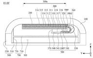
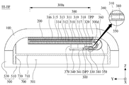
도 1은 본 출원의 일 예에 따른 플렉서블 회로 필름을 나타내는 평면도이다.
도 2는 도 1에 도시된 선 I-I'의 단면도이다.
도 3은 본 출원의 일 예에 따른 전자 기기를 나타내는 평면도이다.
도 4는 도 3에 도시된 커버 윈도우의 후면을 나타내는 도면이다.
도 5는 도 3에 도시된 선 II-II'의 단면도이다.
도 6은 도 3에 도시된 선 III-III'의 단면도이다.
도 7은 도 3에 도시된 선 II-II'의 다른 단면도이다.
도 8a 내지 도 8c는 본 출원의 일 예에 따른 전자 기기에서, 커버 윈도우와 디스플레이 모듈의 본딩 공정과 디스플레이 모듈의 벤딩 공정을 나타내는 공정 순서도이다.1 is a plan view showing a flexible circuit film according to an example of the present application.
FIG. 2 is a cross-sectional view of line I-I 'shown in FIG. 1.
3 is a plan view illustrating an electronic device according to an example of the present application.
FIG. 4 is a view showing the rear surface of the cover window shown in FIG. 3.
5 is a cross-sectional view taken along line II-II 'shown in FIG. 3.
6 is a cross-sectional view taken along line III-III 'shown in FIG. 3.
7 is another cross-sectional view of line II-II 'shown in FIG. 3.
8A to 8C are process flowcharts illustrating a bonding process of a cover window and a display module and a bending process of a display module in an electronic device according to an example of the present application.
본 출원의 이점 및 특징, 그리고 그것들을 달성하는 방법은 첨부되는 도면과 함께 상세하게 후술되어 있는 일 예들을 참조하면 명확해질 것이다. 그러나 본 출원은 이하에서 개시되는 일 예들에 한정되는 것이 아니라 서로 다른 다양한 형태로 구현될 것이며, 단지 본 출원의 일 예들은 본 출원의 개시가 완전하도록 하며, 본 출원의 발명이 속하는 기술분야에서 통상의 지식을 가진 자에게 발명의 범주를 완전하게 알려주기 위해 제공되는 것이며, 본 출원의 발명은 청구항의 범주에 의해 정의될 뿐이다.Advantages and features of the present application, and a method of achieving them will be clarified with reference to examples described below in detail together with the accompanying drawings. However, the present application is not limited to the examples disclosed below, but will be implemented in various different forms, and only the examples of the present application allow the disclosure of the present application to be complete, and are generally in the art to which the invention of the present application pertains. It is provided to fully inform the person of knowledge of the scope of the invention, and the invention of the present application is only defined by the scope of the claims.
본 출원의 일 예를 설명하기 위한 도면에 개시된 형상, 크기, 비율, 각도, 개수 등은 예시적인 것이므로 본 출원이 도시된 사항에 한정되는 것은 아니다. 명세서 전체에 걸쳐 동일 참조 부호는 동일 구성 요소를 지칭한다. 또한, 본 출원의 예를 설명함에 있어서, 관련된 공지 기술에 대한 구체적인 설명이 본 출원의 요지를 불필요하게 흐릴 수 있다고 판단되는 경우 그 상세한 설명은 생략한다.The shapes, sizes, ratios, angles, numbers, etc. disclosed in the drawings for explaining an example of the present application are exemplary, and the present application is not limited to the illustrated matters. The same reference numerals refer to the same components throughout the specification. In addition, in describing an example of the present application, when it is determined that a detailed description of related known technologies may unnecessarily obscure the subject matter of the present application, the detailed description will be omitted.
본 명세서에서 언급된 '포함한다', '갖는다', '이루어진다' 등이 사용되는 경우 '~만'이 사용되지 않는 이상 다른 부분이 추가될 수 있다. 구성 요소를 단수로 표현한 경우에 특별히 명시적인 기재 사항이 없는 한 복수를 포함하는 경우를 포함한다.When 'include', 'have', 'consist of' and the like mentioned in this specification are used, other parts may be added unless '~ man' is used. When a component is expressed as a singular number, the plural number is included unless otherwise specified.
구성 요소를 해석함에 있어서, 별도의 명시적 기재가 없더라도 오차 범위를 포함하는 것으로 해석한다.In interpreting the components, it is interpreted as including the error range even if there is no explicit description.
위치 관계에 대한 설명일 경우, 예를 들어, '~상에', '~상부에', '~하부에', '~옆에' 등으로 두 부분의 위치 관계가 설명되는 경우, '바로' 또는 '직접'이 사용되지 않는 이상 두 부분 사이에 하나 이상의 다른 부분이 위치할 수도 있다.In the case of the description of the positional relationship, for example, when the positional relationship of two parts is described as '~ top', '~ upper', '~ bottom', '~ side', etc., 'right' Alternatively, one or more other parts may be located between the two parts unless 'direct' is used.
시간 관계에 대한 설명일 경우, 예를 들어, '~후에', '~에 이어서', '~다음에', '~전에' 등으로 시간적 선후 관계가 설명되는 경우, '바로' 또는 '직접'이 사용되지 않는 이상 연속적이지 않은 경우도 포함할 수 있다.In the case of a description of a time relationship, for example, 'after', 'following', '~ after', '~ before', etc. When a temporal sequential relationship is described, 'right' or 'direct' It may also include cases that are not continuous unless it is used.
제 1, 제 2 등이 다양한 구성요소들을 서술하기 위해서 사용되나, 이들 구성요소들은 이들 용어에 의해 제한되지 않는다. 이들 용어들은 단지 하나의 구성요소를 다른 구성요소와 구별하기 위하여 사용하는 것이다. 따라서, 이하에서 언급되는 제 1 구성요소는 본 출원의 기술적 사상 내에서 제 2 구성요소일 수도 있다.The first, second, etc. are used to describe various components, but these components are not limited by these terms. These terms are only used to distinguish one component from another component. Accordingly, the first component mentioned below may be the second component within the technical spirit of the present application.
"적어도 하나"의 용어는 하나 이상의 관련 항목으로부터 제시 가능한 모든 조합을 포함하는 것으로 이해되어야 한다. 예를 들어, "제 1 항목, 제 2 항목 및 제 3 항목 중에서 적어도 하나"의 의미는 제 1 항목, 제 2 항목 또는 제 3 항목 각각 뿐만 아니라 제 1 항목, 제 2 항목 및 제 3 항목 중에서 2개 이상으로부터 제시될 수 있는 모든 항목의 조합을 의미할 수 있다. It should be understood that the term “at least one” includes all possible combinations from one or more related items. For example, the meaning of "at least one of the first item, the second item, and the third item" means 2 of the first item, second item, or third item, as well as the first item, second item, and third item, respectively. It can mean any combination of items that can be presented from more than one dog.
본 출원의 여러 예들의 각각 특징들이 부분적으로 또는 전체적으로 서로 결합 또는 조합 가능하고, 기술적으로 다양한 연동 및 구동이 가능하며, 각 예들이 서로에 대하여 독립적으로 실시 가능할 수도 있고 연관 관계로 함께 실시할 수도 있다.Each of the features of the various examples of the present application may be partially or totally combined or combined with each other, technically various interlocking and driving may be possible, and each of the examples may be independently implemented with respect to each other or may be implemented together in an associative relationship. .
이하에서는 본 출원에 따른 플렉서블 회로 필름 및 이를 포함하는 전자 기기의 바람직한 예를 첨부된 도면을 참조하여 상세히 설명한다. 각 도면의 구성요소들에 참조부호를 부가함에 있어서, 동일한 구성요소들에 대해서는 비록 다른 도면상에 표시되더라도 가능한 한 동일한 부호를 가질 수 있다Hereinafter, preferred examples of the flexible circuit film and the electronic device including the same according to the present application will be described in detail with reference to the accompanying drawings. In adding reference numerals to the components of each drawing, the same components may have the same reference numerals as possible even though they are displayed on different drawings.
도 1은 본 출원의 일 예에 따른 플렉서블 회로 필름을 나타내는 평면도이며, 도 2는 도 1에 도시된 선 I-I'의 단면도이다.1 is a plan view showing a flexible circuit film according to an example of the present application, and FIG. 2 is a cross-sectional view of line I-I 'shown in FIG. 1.
도 1 및 도 2를 참조하면, 본 출원의 일 예에 따른 플렉서블 회로 필름(10)은 조립 공정에서 꺽임이 방지되거나 벤딩 반발력이 감소될 수 있는 구조를 포함할 수 있다. 일 예에 따른 플렉서블 회로 필름(10)은 적어도 하나의 본딩 패드부(P1), 몸체부(P3), 및 적어도 하나의 본딩 패드부(P1)와 몸체부(P3) 간에 연결된 필름 벤딩부(P2)를 포함할 수 있다. 여기서, 필름 벤딩부(P2)의 적어도 일부는 몸체부(P3)의 두께보다 얇은 두께를 가짐으로써 조립 공정에서 플렉서블 회로 필름(10)의 꺽임을 방지하거나 벤딩된 플렉서블 회로 필름(10)의 벤딩 반발력을 감소시킬 수 있다.1 and 2, the
상기 적어도 하나의 본딩 패드부(P1)와 필름 벤딩부(P2) 및 몸체부(P3) 각각은 복층 구조를 가질 수 있으며, 이 경우, 필름 벤딩부(P2)의 적어도 일부는 몸체부(P3)보다 적은 층수를 가질 수 있다. 예를 들어, 필름 벤딩부(P2)의 적어도 일부는 4층 이하의 복층 구조를 가질 수 있으며, 몸체부(P3)는 5층 이상의 복층 구조를 가질 수 있다.Each of the at least one bonding pad portion P1, the film bending portion P2, and the body portion P3 may have a multi-layer structure, in which case, at least a portion of the film bending portion P2 is a body portion P3 It may have fewer floors. For example, at least a portion of the film bending portion P2 may have a multi-layer structure of 4 layers or less, and the body portion P3 may have a multi-layer structure of 5 layers or more.
상기 적어도 하나의 본딩 패드부(P1)는 디스플레이 모듈의 디스플레이 패드부 또는 터치 패드부와 전기적으로 연결될 수 있다. 예를 들어, 적어도 하나의 본딩 패드부(P1)는 이방성 도전 필름을 매개로 하는 필름 부착 공정에 의해 디스플레이 모듈의 디스플레이 패드부 또는 터치 패드부와 전기적으로 연결될 수 있다.The at least one bonding pad part P1 may be electrically connected to a display pad part or a touch pad part of the display module. For example, the at least one bonding pad portion P1 may be electrically connected to the display pad portion or the touch pad portion of the display module by a film attachment process via an anisotropic conductive film.
상기 몸체부(P3)는 일정한 길이를 갖는 플렉서블 회로 필름(10)의 몸체로서, 회로 배선과 회로 부품 등을 포함할 수 있다. 일 예에 따른 몸체부(P3)는 플렉서블 회로 필름(10)의 길이에 따라 제 1 내지 제 3 몸체부(P3a, P3b, P3c), 전자 부품 실장부(P3d), 및 제 4 몸체부(P3e)를 포함할 수 있다. 전자 부품 실장부(P3d)는 표면 실장 기술에 의해 실장된 각종 전자 부품(또는 회로)을 포함할 수 있다.The body portion P3 is a body of the
상기 필름 벤딩부(P2)는 적어도 하나의 본딩 패드부(P1)와 몸체부(P3)의 제 1 몸체부(P3a) 사이에 배치되어 플렉서블 회로 필름(10)의 벤딩을 가능하게 한다.The film bending part P2 is disposed between at least one bonding pad part P1 and the first body part P3a of the body part P3 to allow bending of the
일 예에 따른 플렉서블 회로 필름(10)은 커넥터부(P4)를 더 포함할 수 있다. 상기 커넥터부(P4)는 몸체부(P3)의 제 4 몸체부(P3e)로부터 연장되어 전자 기기의 인쇄 회로 기판과 전기적으로 접속될 수 있다.The
일 예에 따른 플렉서블 회로 필름(10)은 베이스 부재(11), 회로 배선층(12), 커버층(13), 및 코팅층(14)을 포함할 수 있다.The
상기 베이스 부재(11)는 플렉서블 회로 필름(10)의 적어도 하나의 본딩 패드부(P1), 필름 벤딩부(P2), 몸체부(P3), 및 커넥터부(P4) 각각과 중첩되도록 배치될 수 있다. 즉, 베이스 부재(11)는 적어도 하나의 본딩 패드부(P1), 필름 벤딩부(P2), 몸체부(P3), 및 커넥터부(P4) 각각과 대응되는 영역을 포함할 수 있다. 일 예에 따른 베이스 부재(11)는 플라스틱 필름, 예를 들어 PI(polyimide) 필름일 수 있다.The
상기 회로 배선층(12)은 동박 적층체(Copper Clad Laminaion) 구조 또는 플렉서블 동박 적층체(Flexible Copper Clad Laminaion) 구조를 가지도록 베이스 부재(11)의 일면(또는 전면)과 타면(또는 후면) 중 적어도 하나에 배치될 수 있다.The
일 예에 따른 회로 배선층(12)은 베이스 부재(11)의 일면 상에 배치된 제 1 회로 배선층(12a)을 포함할 수 있다.The
상기 제 1 회로 배선층(12a)은 동박 적층체 구조 또는 플렉서블 동박 적층체 구조를 가지도록 베이스 부재(11)의 일면 상에 배치된 복수의 제 1 회로 배선을 포함할 수 있다. 즉, 제 1 회로 배선층(12a)은 베이스 부재(11)의 일면 전체에 배치됨으로써 플렉서블 회로 필름(10)의 적어도 하나의 본딩 패드부(P1), 필름 벤딩부(P2), 몸체부(P3), 및 커넥터부(P4) 각각과 중첩될 수 있다.The first
일 예에 따른 제 1 회로 배선층(12a)은 접착층을 매개로 베이스 부재(11)의 일면에 부착된 동박층을 포함함으로써 실질적으로 접착층과 동박층으로 이루어진 2층 구조를 가질 수 있지만, 접착층과 동박층의 적층(또는 결합) 구조를 갖는 제 1 회로 배선층(12a)은 하나의 층으로 해석할 수 있다.The first
다른 예에 따른 제 1 회로 배선층(12a)은 베이스 부재(11)의 일면에 부착된 접착층과 접착층 상에 배치된 복수의 동박층 및 복수의 동박층 사이에 개재된 절연층(또는 절연 접착층)을 포함할 수 있지만, 이 경우에도 제 1 회로 배선층(12a)은 하나의 층으로 해석할 수 있다.The first
일 예에 따른 회로 배선층(12)은 베이스 부재(11)의 타면 상에 배치된 제 2 회로 배선층(12b)과 제 3 회로 배선층(12c)을 더 포함할 수 있다. The
상기 제 2 회로 배선층(12b)는 동박 적층체 구조 또는 플렉서블 동박 적층체 구조를 가지도록 베이스 부재(11)의 타면 상에 배치된 복수의 제 2 회로 배선을 포함할 수 있다. 즉, 제 2 회로 배선층(12b)은 몸체부(P3)의 제 1 몸체부(P3a)와 제 3 몸체부(P3c) 및 전자 부품 실장부(P3d) 각각과 중첩되는 베이스 부재(11)의 타면 상에 배치될 수 있다. 여기서, 제 2 회로 배선층(12b)은 몸체부(P3)의 전자 부품 실장부(P3d)에 배치되며, 플렉서블 회로 필름(10)의 회로 구성에 따라 몸체부(P3)의 제 1 내지 제 4 몸체부(P3a, P3b, P3c, P3e) 중 적어도 하나에 추가로 배치될 수 있다.The second
일 예에 따른 제 2 회로 배선층(12b)은 접착층을 매개로 베이스 부재(11)의 타면에 부착된 동박층을 포함함으로써 실질적으로 접착층과 동박층으로 이루어진 2층 구조를 가질 수 있지만, 접착층과 동박층의 적층(또는 결합) 구조를 갖는 제 2 회로 배선층(12b)은 하나의 층으로 해석할 수 있다.The second
다른 예에 따른 제 2 회로 배선층(12b)은 베이스 부재(11)의 타면에 부착된 접착층과 접착층 상에 배치된 복수의 동박층 및 복수의 동박층 사이에 개재된 절연층(또는 절연 접착층)을 포함할 수 있지만, 이 경우에도 제 2 회로 배선층(12b)은 하나의 층으로 해석할 수 있다.The second
부가적으로, 제 2 회로 배선층(12b)에 배치된 복수의 제 2 회로 배선 중 적어도 일부는 베이스 부재(11)를 관통하는 비아홀 또는 컨택홀을 통해서 제 1 회로 배선층(12a)에 배치된 복수의 제 1 회로 배선 중 적어도 하나와 전기적으로 연결될 수 있다.Additionally, at least some of the plurality of second circuit wires disposed in the second
상기 제 3 회로 배선층(12c)는 동박 적층체 구조 또는 플렉서블 동박 적층체 구조를 가지도록 제 2 회로 배선층(12b) 상에 배치된 복수의 제 3 회로 배선을 포함할 수 있다.The third
일 예에 따른 제 3 회로 배선층(12c)은 접착층을 매개로 제 2 회로 배선층(12b) 상에 배치된 동박층을 포함함으로써 실질적으로 접착층과 동박층으로 이루어진 2층 구조를 가질 수 있지만, 접착층과 동박층의 적층(또는 결합) 구조를 갖는 제 3 회로 배선층(12c)은 하나의 층으로 해석할 수 있다.The third
다른 예에 따른 제 3 회로 배선층(12b)은 제 2 회로 배선층(12b) 상에 배치된 접착층과 접착층 상에 배치된 복수의 동박층 및 복수의 동박층 사이에 개재된 절연층(또는 절연 접착층)을 포함할 수 있지만, 이 경우에도 제 3 회로 배선층(12c)은 하나의 층으로 해석할 수 있다.The third
부가적으로, 제 3 회로 배선층(12c)에 배치된 복수의 제 3 회로 배선 중 적어도 일부는 제 2 회로 배선층(12b)에 배치된 복수의 제 2 회로 배선 중 적어도 일부 및/또는 제 2 회로 배선층(12b)과 베이스 부재(11)를 관통하는 비아홀 또는 컨택홀을 통해서 제 1 회로 배선층(12a)에 배치된 복수의 제 1 회로 배선 중 적어도 하나와 전기적으로 연결될 수 있다.Additionally, at least a portion of the plurality of third circuit wirings arranged in the third
상기 커버층(13)은 몸체부(P3) 상에 배치된 회로 배선층(12)을 덮음으로써 회로 배선층(12)의 외부 노출을 방지한다.The
일 예에 따른 커버층(13)은 몸체부(P3)와 중첩되는 베이스 부재(11)의 일면 상에 배치된 제 1 회로 배선층(12a)을 덮는 제 1 커버층(13a)을포함할 수 있다.The
상기 제 1 커버층(13a)은 커버 필름 및 커버 필름의 일면에 코팅된 접착층을 포함하는 2층 구조를 가질 수 있지만, 이 경우에도 제 1 커버층(13a)은 하나의 층으로 해석할 수 있다. 이러한 제 1 커버층(13a)은 접착층을 매개로 몸체부(P3)와 중첩되는 베이스 부재(11)의 일면 상에 배치된 제 1 회로 배선층(12a) 상에 부착됨으로써 제 1 회로 배선층(12a)의 노출면을 보호하거나 절연시킬 수 있다. 일 예로서, 제 1 커버층(13a)은 PI 필름 및 PI 필름의 일면에 코팅된 열경화성 에폭시 접착제를 포함하는 복합 필름일 수 있다. 다른 예로서, 제 1 커버층(13a)은 PI 필름, PI 필름의 일면에 형성된 열경화성 에폭시 접착제, 및 PI 필름의 타면에 형성된 블랙 접착제(또는 블랙 PI 필름)을 포함하는 복합 필름일 수 있다.The
일 예에 따른 커버층(13)은 몸체부(P3)와 중첩되는 베이스 부재(11)의 타면 상에 배치된 제 2 회로 배선층(12b)을 덮는 제 2 커버층(13b)을 더 포함할 수 있다. 이러한 제 2 커버층(13b)은 제 1 커버층(13a)와 동일한 구조를 가지거나 제 1 커버층(13a)와 동일한 구조를 가지면서 제 1 커버층(13a)보다 얇은 두께를 가질 수 있다. 추가적으로, 제 2 커버층(13b)은 제 2 회로 배선층(12b)이 배치되지 않은 몸체부(P3)의 제 4 몸체부(P3e) 및 커넥터부(P4)에 추가로 배치될 수 있다. 즉, 제 2 커버층(13b)은 몸체부(P3) 중 제 2 몸체부(P3b)를 제외한 나머지 부분(P3a, P3c, P3d, P3e)과 중첩되는 제 2 회로 배선층(12b) 상에 배치됨과 동시에 커넥터부(P4)와 중첩되는 베이스 부재(11)의 타면 상에 배치될 수 있다.The
일 예에 따른 커버층(13)은 몸체부(P3)의 제 4 몸체부(13e)와 커넥터부(P4)에 중첩되는 베이스 부재(11)의 타면 상에 배치된 제 3 커버층(13c)을 더 포함할 수 있다. 이러한 제 3 커버층(13c)은 제 1 커버층(13a)와 동일한 구조를 가질 수 있다.The
상기 코팅층(14)은 필름 벤딩부(P2)의 적어도 일부와 중첩되는 베이스 부재(11)의 일면 상에 코팅되어 경화될 수 있다. 이러한 코팅층(14)은 필름 벤딩부(P2) 상에 배치된 회로 배선층(12)의 제 1 회로 배선층(12a)을 덮음으로써 커버층(13)에 의해 덮이지 않는 제 1 회로 배선층(12a)의 노출면을 보호하거나 절연시킬 수 있다.The
상기 코팅층(14)은 필름 벤딩부(P2)의 적어도 일부가 몸체부(P3)의 두께보다 얇은 두께를 가지도록 필름 벤딩부(P2)의 적어도 일부에 형성됨으로써 조립 공정에서 플렉서블 회로 필름(10)의 강제적인 꺽임을 방지하거나 벤딩된 플렉서블 회로 필름(10)의 벤딩 반발력을 감소시킬 수 있다.The
일 예에 따른 코팅층(14)의 두께는 커버층(13)의 두께보다 얇을 수 있다. 즉, 코팅층(14)의 두께는 커버층(13)의 제 1 내지 제 3 커버층(13a, 13b, 13c) 각각보다 얇은 두께를 가질 수 있다. 일 예로서, 코팅층(14)은 제 1 회로 배선층(12a)의 노출면을 보호하거나 절연시키기 위한 최소 두께보다 두껍고 제 1 커버층(13a)의 두께보다 얇은 두께를 가질 수 있으며, 이 경우, 코팅층(14)은 5 마이크로미터 이상의 두께를 가질 수 있다. 다른 예로서, 필름 벤딩부(P2)에서, 베이스 부재(11)의 전면으로부터 코팅층(14)의 최상면까지의 제 1 높이는 베이스 부재(11)의 전면으로부터 제 1 커버층(13a)의 최상면까지의 제 2 높이보다 낮을 수 있다.The thickness of the
실험에 따르면, 20마이크로미터의 두께를 갖는 코팅층(14)이 필름 벤딩부(P2)의 적어도 일부에 형성된 제 1 실험 예에 따른 필름 벤딩부(P2)의 벤딩 반발력은 37.5마이크로미터의 두께를 갖는 제 1 커버층(13a)이 필름 벤딩부(P2)의 적어도 일부에 형성된 제 2 실험 예에 따른 필름 벤딩부(P2)의 벤딩 반발력보다 23% 정도 감소하는 것을 확인할 수 있었다.According to the experiment, the bending reaction force of the film bending portion P2 according to the first experimental example in which the
일 예에 따른 코팅층(14)은 제 1 회로 배선층(12a)의 노출면을 보호하거나 절연시키기 위한 절연 물질로 이루어질 수 있다. 예를 들어, 코팅층(14)은 PI 물질 또는 솔더 레지스트 물질을 포함할 수 있다.The
본 출원에 따른 플렉서블 회로 필름(10)은 코팅층(14)의 형성 공정에서 필름 벤딩부(P2)에 도포되는 절연 물질(또는 코팅 물질)의 일부가 본딩 패드부(P1)의 패드 쪽으로 흘러 넘치는 것을 최소화하기 위한 격벽(15)을 더 포함할 수 있다.In the
상기 격벽(15)은 필름 벤딩부(P2)에 접한 본딩 패드부(P1)의 일측 상에 일정한 높이(또는 두께)를 가지도록 형성됨으로써 필름 벤딩부(P2)에 도포되는 절연 물질(또는 코팅 물질)의 일부가 본딩 패드부(P1)의 패드 쪽으로 흘러 넘치는 것을 최소화할 수 있다. 이때, 코팅층(14)은 본딩 패드부(P1)와 필름 벤딩부(P2)의 경계부를 덮도록 필름 벤딩부(P2)에 접한 격벽(15)의 일측 상에도 형성될 수 있다. 예를 들어, 코팅층(14)은 필름 벤딩부(P2) 전체를 덮도록 형성됨과 동시에 본딩 패드부(P1)와 필름 벤딩부(P2)의 경계부를 덮도록 형성될 수 있다. 즉, 코팅층(14)은 필름 벤딩부(P2)에 도포되는 절연 물질(또는 코팅 물질)의 도포량에 따라 필름 벤딩부(P2)에 접한 격벽(15)의 일측을 덮도록 형성될 수 있다.The
일 예에 따른 격벽(15)은 공정의 편의성을 위해, 커버층(13)과 동일한 물질로 이루어질 수 있다. 즉, 격벽(15)은 커버층(13)의 제 1 커버층(13a)와 동일한 물질로 이루어져 제 1 커버층(13a)과 동일한 공정에 의하여 함께 형성될 수 있다.The
본 출원에 따른 플렉서블 회로 필름(10)은 지지 플레이트(16), 정전기 차폐층(17), 전도성 접착 부재(18), 금속 플레이트(19), 접착 시트(20), 접지 플레이트(21), 회로 보호층(22), 방열층(23), 및 스티프너(stiffener)(24)를 더 포함할 수 있다.The
상기 지지 플레이트(16)는 회로층(12)의 제 1 회로 배선층(12a) 전체를 덮는다. 이 경우, 지지 플레이트(16)는 베이스 부재(11)와 동일한 형태를 가지도록 형성되고, 접착제를 매개로 회로층(12)의 제 1 회로 배선층(12a)에 부착될 수 있다. 이때, 지지 플레이트(16)는 접착제를 매개로 제 1 회로 배선층(12a)에 부착됨에 따라 실질적으로 2층 구조를 가지지만, 접착제를 포함하는 지지 플레이트(16)는 하나의 층으로 해석할 수 있다. 이러한 지지 플레이트(16) 상에는 상기 코팅층(14)과 격벽(15) 및 커버층(13)의 제 1 커버층(13a)이 배치될 수 있다.The
상기 정전기 차폐층(17)은 몸체부(P3)의 제 1 내지 제 3 몸체부(13a, 13b, 13c)와 중첩되는 커버층(13)의 제 1 커버층(13a) 상에 배치될 수 있다. 일 예에 따른 정전기 차폐층(17)은 도전성접착층, 도전성접착층 상에 합지된 쉴드층, 및 쉴드층 상에 합지된 보호층을 포함할 수 있다. 정전기 차폐층(17)은 하나의 층으로 해석할 수 있다.The
상기 전도성 접착 부재(18)는 몸체부(P3)의 회로 부품 실장부(P3d)와 중첩되는 커버층(13)의 제 1 커버층(13a) 상에 배치될 수 있다. 일 예에 따른 전도성 접착 부재(18)는 등방도전성접착제를 포함할 수 있다.The
상기 금속 플레이트(19)는 전도성 접착 부재(18) 상에 배치될 수 있다. 일 예에 따른 금속 플레이트(19)는 스테인리스 재질을 포함할 수 있으며, 전도성 접착 부재(18)를 통해 몸체부(P3)의 회로 부품 실장부(P3d)에 마련된 접지 패드와 전기적으로 연결될 수 있다. 이러한 금속 플레이트(19)는 회로 부품 실장부(P3d)의 강도를 보강하는 역할 및 방열 기능을 겸할 수 있다.The
상기 접착 시트(20)는 커버층(13)의 제 2 커버층(13b)을 덮도록 배치될 수 있다. 즉, 접착 시트(20)는 제 2 커버층(13b)과 제 3 회로 배선층(12c) 사이에 배치되면서 제 2 커버층(13b)와 제 3 커버층(13c) 사이에 배치될 수 있다. 이러한 접착 시트(20)는 제 2 커버층(13b)과 제 3 회로 배선층(12c)을 서로 합지시키고 제 2 커버층(13b)과 제 3 커버층(13c)을 서로 합지시키는 역할을 할 수 있다.The
상기 접지 플레이트(21)는 회로층(12)의 제 3 회로 배선층(12c) 전체를 덮을 수 있다. 이 경우, 접지 플레이트(21)는 제 3 회로 배선층(12c)과 동일한 형태를 가지도록 형성되고, 접착제를 매개로 제 3 회로 배선층(12c)에 부착될 수 있다. 이때, 접지 플레이트(21)는 접착제를 매개로 제 3 회로 배선층(12c)에 부착됨에 따라 실질적으로 2층 구조를 가지지만, 접착제를 포함하는 접지 플레이트(21)는 하나의 층으로 해석할 수 있다.The
상기 회로 보호층(22)은 몸체부(P3)의 제 3 몸체부(P3c) 및 회로 부품 실장부(P3d)와 중첩되는 접지 플레이트(21) 상에 배치될 수 있다. 일 예에 따른 회로 보호층(22)은 사진 현상형 솔더 레지스트(Photo imagable Solder Resist)를 포함할 수 있으며, 녹색의 색상을 가질 수 있으나, 반드시 이에 한정되지 않는다.The
상기 방열층(23)은 몸체부(P3)의 제 1 내지 제 3 몸체부(P3a, P3b, P3c)와 중첩하도록 배치될 수 있다. 예를 들어, 방열층(23)은 제 1 및 제 3 몸체부(P3a, P3c)와 중첩되는 접지 플레이트(21), 제 1 내지 제 3 몸체부(P3a, P3b, P3c)와 중첩되는 베이스 부재(11), 및 제3 몸체부(P3c)와 중첩되는 회로 보호층(22)를 덮도록 배치될 수 있다. 일 예에 따른 방열층(23)은 상대적으로 높은 열전도율을 갖는 물질로 이루어질 수 있다. 예를 들어, 방열층(23)은 은(Ag) 재질로 이루어진 방열 플레이트를 포함할 수 있다.The
상기 스티프너(24)는 커넥터부(P4)와 중첩되는 커버층(13)의 제 3 커버층(13c) 상에 배치되어 커넥터부(P4)의 강도를 보강할 수 있다. 일 예에 따른 스티프너(24)는 PET, PI, 또는 에폭시를 포함할 수 있다.The
이와 같은, 본 출원의 일 예에 따른 플렉서블 회로 필름(10)은 필름 벤딩부(P2)의 적어도 일부가 몸체부(P3)의 두께보다 얇은 두께를 가짐으로써 조립 공정에서 플렉서블 회로 필름(10)의 꺽임이 방지되거나 벤딩된 플렉서블 회로 필름(10)의 벤딩 반발력이 감소될 수 있다.As such, the
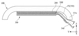
도 3은 본 출원의 일 예에 따른 전자 기기를 나타내는 평면도이고, 도 4는 도 3에 도시된 커버 윈도우의 후면을 나타내는 도면이고, 도 5는 도 3에 도시된 선 II-II'의 단면도이며, 도 6은 도 3에 도시된 선 III-III'의 단면도이다. 도 5 및 도 6에 도시된 디스플레이 모듈(300), 터치 플렉서블 회로 필름(350), 및 커버 윈도우(100) 각각은 설명의 편의를 위해 실제와 다른 스케일로 도시한 것으므로, 도면에 도시된 스케일에 한정되지 않는다.3 is a plan view illustrating an electronic device according to an example of the present application, FIG. 4 is a view showing a rear surface of the cover window shown in FIG. 3, and FIG. 5 is a cross-sectional view of line II-II 'shown in FIG. 3 , FIG. 6 is a cross-sectional view of line III-III 'shown in FIG. 3. Each of the
도 3 내지 도 6을 참조하면, 본 출원의 일 예에 따른 전자 기기는 커버 윈도우(100), 디스플레이 모듈(300), 및 하우징(500)을 포함할 수 있다.3 to 6, an electronic device according to an example of the present application may include a
상기 커버 윈도우(100)는 디스플레이 모듈(300)의 전면(前面)과 측면을 덮음으로써 외부 충격으로부터 디스플레이 모듈(300)을 보호하는 역할을 할 수 있다.The
일 예에 따른 커버 윈도우(100)는 투명 플라스틱 재질, 글라스 재질, 또는 강화 글라스 재질로 이루어질 수 있다. 일 예로서, 커버 윈도우(100)는 사파이어 글라스(Sapphire Glass) 및 고릴라 글라스(Gorilla Glass) 중 어느 하나 또는 이들의 적층 구조를 가질 수 있다. 다른 예로서, 커버 윈도우(100)는 PET(polyethyleneterephthalate), PC(polycarbonate), PES(polyethersulfone), PEN(polyethylenapthanate), 및 PNB(polynorborneen) 중 어느 하나의 재질을 포함할 수 있다. 커버 윈도우(100)는 긁힘과 투명도를 고려하여 강화 글라스로 이루어질 수 있다.The
일 예에 따른 커버 윈도우(100)는 전면부(110), 전면부(110)의 가장자리 부분으로부터 만곡된 제 1 내지 제 4 측벽부(131a, 131b, 131c, 131d), 및 제 1 내지 제 4 측벽부(131a, 131b, 131c, 131d) 사이에 만곡된 제 1 내지 제 4 모서리부(133a, 133b, 133c, 133d)를 포함할 수 있다.The
상기 전면부(110)는 커버 윈도우(100)의 중앙 부분으로서, 광이 투과되는 투명 영역일 수 있다. 전면부(110)는 전체적으로 평면 형태를 가질 수 있다.The
상기 제 1 내지 제 4 측벽부(131a, 131b, 131c, 131d) 각각은 전면부(110)의 가장자리 부분으로부터 미리 설정된 곡률 반경을 가지도록 만곡된다. 이에 따라, 전면부(110)의 가장자리 부분은 전체적으로 만곡된 구조를 가질 수 있다.Each of the first to fourth
상기 제 1 및 제 2 측벽부(131a, 131b) 각각은 커버 윈도우(100)의 장변 길이 방향(Y)을 따라 서로 나란하게 배치될 수 있다. 제 1 및 제 2 측벽부(131a, 131b) 각각은 서로 동일한 곡률 반경을 가지도록 만곡되거나 서로 다른 곡률 반경을 가지도록 만곡될 수 있다.Each of the first and
상기 제 3 및 제 4 측벽부(131c, 131d) 각각은 커버 윈도우(100)의 단변 길이 방향(X)을 따라 서로 나란하게 배치될 수 있다. 제 3 및 제 4 측벽부(131c, 131d) 각각은 서로 동일한 곡률 반경을 가지도록 만곡되거나 서로 다른 곡률 반경을 가지도록 만곡될 수 있다.Each of the third and
상기 제 1 내지 제 4 모서리부(133a, 133b, 133c, 133d) 각각은 인접한 측벽부(131a, 131b, 131c, 131d) 사이에 곡면 형태로 형성될 수 있다.Each of the first to
이와 같은, 커버 윈도우(100)는 전체적으로 만곡된 4면 벤딩 구조를 가짐으로써 전자 기기의 미감을 개선시킬 수 있으며, 전자 기기의 가로 방향과 세로 방향 각각의 베젤 폭을 감소시킬 수 있다.As such, the
추가적으로, 커버 윈도우(100)는 가장자리 부분에 마련된 디자인층(또는 데코레이션층)을 더 포함할 수 있다. 디자인층은 디스플레이 모듈(300)과 마주하는 커버 윈도우(100)의 후면(또는 배면) 가장자리 부분에 적어도 1회 프린팅됨으로써 전자 기기에서 영상이 표시되는 않는 비표시 영역을 감출 수 있다.Additionally, the
상기 디스플레이 모듈(300)은 평판 디스플레이 장치의 디스플레이 패널이 될 수 있다. 이하의 설명에서는 디스플레이 모듈(300)이 플렉서블 발광 디스플레이 모듈인 것으로 가정하여 설명하기로 한다.The
상기 디스플레이 모듈(300)은 커버 윈도우(100)의 후면(또는 배면)에 결합되어 영상을 표시하거나 사용자 터치를 센싱할 수 있다. 디스플레이 모듈(300)은 모듈 본딩 부재(200)를 이용한 다이렉트 본딩 공정을 통해 커버 윈도우(100)의 전면부(110)의 후면에 본딩될 수 있다. 여기서, 모듈 본딩 부재(200)는 PSA(pressure sensitive adhesive), OCA(optical clear adhesive) 또는 OCR(optical clear resin)을 포함할 수 있다.The
일 예에 따른 디스플레이 모듈(300)은 표시부(300a), 제 1 벤딩 표시부(300b), 및 제 2 벤딩 표시부(300c)를 포함할 수 있다.The
상기 표시부(300a)는 커버 윈도우(100)의 전면부 쪽으로 영상을 표시할 수 있다. 제 1 벤딩 표시부(300b)는 표시부(300a)의 제 1 측 가장자리로부터 곡면 형태로 벤딩되어 커버 윈도우(100)의 제 1 측벽부(131a) 쪽으로 영상을 표시할 수 있다. 제 2 벤딩 표시부(300c)는 표시부(300a)의 제 2 측 가장자리로부터 곡면 형태로 벤딩되어 커버 윈도우(100)의 제 2 측벽부(131b) 쪽으로 영상을 표시할 수 있다. 선택적으로, 제 1 벤딩 표시부(300b)과 제 2 벤딩 표시부(300c)는 생략 가능하다.The
일 예에 따른 디스플레이 모듈(300)은 플렉서블 기판(310), 화소 어레이부(311), 디스플레이 패드부(DPP), 봉지부(312), 터치 전극부(314), 터치 패드부(TPP), 기능성 필름(316), 제 1 백 플레이트(317), 제 2 백 플레이트(318), 방열부(319), 벤딩 유지 부재(320), 구동 집적 회로(330), 인쇄 회로 기판(340), 및 터치 플렉서블 회로 필름(350)을 포함할 수 있다.The
상기 플렉서블 기판(310)은 디스플레이 모듈(300)의 베이스 기판으로 정의될 수 있다. 일 예에 따른 플렉서블 기판(310)는 유연성을 갖는 플라스틱 재질, 예를 들어, PI(polyimide), PET(polyethyleneterephthalate), PC(polycarbonate), PES(polyethersulfone), PEN(polyethylenapthanate), PNB(polynorborneen), PMP(polymethylpentene), PMMA(poly methyl methacrylate), 및 COC(cycloolefin copolymer) 중 어느 하나의 재질을 포함할 수 있으며, 보다 바람직하게는 불투명 또는 유색의 PI(polyimide)를 포함할 수 있다. 다른 예에 따른 플렉서블 기판(310)은 유연성을 갖는 박형 글라스 재질로 이루어질 수 있다.The
일 예에 따른 화소 어레이부(311)는 플렉서블 기판(310)에 정의된 표시부(300a)와 제 1 벤딩 표시부(300b) 및 제 2 벤딩 표시부(300c) 상에 형성됨으로써 표시부(300a)와 제 1 벤딩 표시부(300b) 및 제 2 벤딩 표시부(300c) 각각 상에 영상을 표시할 수 있다.The
상기 화소 어레이부(311)는 플렉서블 기판(310) 상에 마련된 신호 라인들에 의해 정의되는 화소 영역에 마련되고 신호 라인들에 공급되는 신호에 따라 영상을 표시하는 복수의 화소를 포함할 수 있다.The
상기 복수의 화소 각각은 화소 영역에 마련된 구동 박막 트랜지스터를 포함하는 화소 회로층, 구동 박막 트랜지스터와 전기적으로 연결된 애노드 전극, 애노드 전극 상에 형성된 발광 소자층, 및 발광 소자층과 전기적으로 연결된 캐소드 전극을 포함할 수 있다.Each of the plurality of pixels includes a pixel circuit layer including a driving thin film transistor provided in a pixel region, an anode electrode electrically connected to the driving thin film transistor, a light emitting device layer formed on the anode electrode, and a cathode electrode electrically connected to the light emitting device layer. It can contain.
상기 구동 박막 트랜지스터는 플렉서블 기판(310) 상에 정의된 각 화소 영역의 트랜지스터 영역에 마련되는 것으로, 게이트 전극, 게이트 절연막, 반도체층, 소스 전극 및 드레인 전극을 포함하여 이루어질 수 있다. 여기서, 박막 트랜지스터의 반도체층은 a-Si, poly-Si, 또는 저온 poly-Si 등의 실리콘을 포함하거나 IGZO(Indium-Gallium-Zinc-Oxide) 등의 산화물을 포함할 수 있다.The driving thin film transistor is provided in the transistor region of each pixel region defined on the
상기 애노드 전극은 각 화소 영역에 정의된 개구 영역에 패턴 형태로 마련되어 구동 박막 트랜지스터와 전기적으로 연결된다The anode electrode is provided in a pattern form in an opening area defined in each pixel area to be electrically connected to a driving thin film transistor.
일 예에 따른 발광 소자층은 애노드 전극 상에 형성된 유기 발광 소자를 포함할 수 있다. 유기 발광 소자는 정공 주입층, 정공 수송층, 유기 발광층, 전자 수송층, 및 전자 주입층이 차례로 적층된 구조로 형성될 수 있다. 여기서, 상기 정공 주입층, 정공 수송층, 전자 수송층 및 전자 주입층 중 하나 또는 둘 이상의 층은 생략이 가능하다. 상기 유기 발광층은 화소 별로 동일한 색, 예로서 화이트(white)의 광을 발광하도록 형성될 수 있고, 화소 별로 상이한 색, 예로서, 적색, 녹색, 또는 청색의 광을 발광하도록 형성될 수도 있다.The light emitting device layer according to an example may include an organic light emitting device formed on the anode electrode. The organic light emitting device may be formed in a structure in which a hole injection layer, a hole transport layer, an organic emission layer, an electron transport layer, and an electron injection layer are sequentially stacked. Here, one or more layers of the hole injection layer, the hole transport layer, the electron transport layer, and the electron injection layer may be omitted. The organic light emitting layer may be formed to emit light of the same color for each pixel, for example, white, or may be formed to emit light of different colors, for example, red, green, or blue for each pixel.
일 예에 따른 발광 소자층은 애노드 전극과 캐소드 전극 각각에 전기적으로 연결된 마이크로 발광 다이오드 소자를 포함할 수 있다. 마이크로 발광 다이오드 소자는 집적 회로(IC) 또는 칩(Chip) 형태로 구현된 발광 다이오드로서, 애노드 전극과 전기적으로 연결된 제 1 단자 및 캐소드 전극과 전기적으로 연결된 제 2 단자를 포함할 수 있다.The light emitting device layer according to an example may include a micro light emitting diode device electrically connected to each of the anode electrode and the cathode electrode. The micro light emitting diode device is a light emitting diode implemented in the form of an integrated circuit (IC) or a chip, and may include a first terminal electrically connected to the anode electrode and a second terminal electrically connected to the cathode electrode.
상기 캐소드 전극은 각 화소 영역에 마련된 발광 소자층의 발광 소자와 공통적으로 연결될 수 있다.The cathode electrode may be commonly connected to light emitting elements of the light emitting element layer provided in each pixel area.
상기 디스플레이 패드부(DPP)는 화소 어레이부(311)의 일측으로부터 멀리 이격된 플렉서블 기판(310)의 일측 가장자리 부분에 마련된 복수의 패드 전극을 포함한다. 복수의 패드 전극 각각은 링크 라인을 통해 화소 어레이부(311)의 신호 라인과 전기적으로 연결된다.The display pad unit DPP includes a plurality of pad electrodes provided on one edge portion of the
상기 봉지부(312)는 화소 어레이부(311)를 둘러싸도록 플렉서블 기판(310) 상에 형성됨으로써 산소 또는 수분이 화소 어레이부(311)의 발광 소자층으로 침투하는 것을 방지할 수 있다. 일 예에 따른 봉지부(312)는 유기 물질층과 무기 물질층이 교대로 적층된 복층 구조로 형성될 수 있다. 여기서, 무기 물질층은 산소 또는 수분이 화소 어레이부(311)의 발광 소자층으로 침투하는 것을 차단하는 역할을 할 수 있다. 그리고, 유기 물질층은 제조 공정 중 발생할 수 있는 이물들(particles)을 덮을 수 있도록 무기 물질층보다 상대적으로 두꺼운 두께로 형성될 수 있다. 예를 들어, 봉지부(312)는 제 1 무기막, 제 1 무기막 상의 유기막, 및 유기막 상의 제 2 무기막을 포함할 수 있다. 이 경우, 유기막은 이물 커버층으로 정의될 수 있다.The
상기 터치 전극부(314)는 봉지부(312) 상에 배치되어 커버 윈도우(100)에 대한 사용자 터치를 센싱하는 터치 센서의 역할을 한다.The
일 예에 따른 터치 전극부(314)는 화소 어레이부(311)와 중첩되는 봉지부(312) 상에 배치된 터치 전극층, 및 터치 전극층을 덮는 유전체층을 포함할 수 있다. 선택적으로, 터치 전극부(314)는 봉지부(312)를 덮는 터치 버퍼층 상에 형성될 수도 있다. 상기 터치 전극층은 화소 어레이부(311)와 중첩되는 봉지부(312) 상에 일정한 간격으로 배치된 복수의 터치 구동 전극, 및 복수의 터치 구동 전극과 전기적으로 절연된 복수의 터치 센싱 전극을 포함할 수 있다. 터치 센싱 전극들은 터치 구동 전극들과 동일층에 배치되거나 유전체층을 사이에 두고 서로 다른 층에 배치될 수 있다.The
다른 예에 따른 터치 전극부(314)는 공지된 정전 용량 방식의 터치 패널로 대체될 수 있으며, 이경우, 터치 패널은 투명 점착 부재(313)를 매개로 봉지부(312) 상에 부착될 수 있다. 여기서, 투명 점착 부재(313)는 PSA(pressure sensitive adhesive), OCA(optical clear adhesive) 또는 OCR(optical clear resin)을 포함할 수 있다.The
상기 터치 패드부(TPP)는 플렉서블 기판(310)의 일측 가장자리에 대응되는 터치 전극부(314)의 일측 가장자리 부분에 배치되어 터치 전극부(314)와 전기적으로 연결된 복수의 터치 패드 전극을 포함할 수 있다. 복수의 터치 패드 전극 각각은 복수의 터치 라우팅 라인을 통해서 터치 센싱 전극들과 터치 구동 전극들과 일대일로 연결될 수 있다. 이러한 터치 패드부(TPP)는 플렉서블 기판(310) 상에 배치된 링크 라인과 중첩될 수 있다. 선택적으로, 터치 패드부(TPP)는 플렉서블 기판(310)의 일측 가장자리에 대응되는 터치 전극부(314)의 일측 가장자리 부분에 배치되어 복수의 터치 라우팅 라인을 통해서 터치 센싱 전극들과 터치 구동 전극들 각각에 일대일로 연결될 수도 있다.The touch pad unit TTP may include a plurality of touch pad electrodes disposed on one edge portion of the
상기 터치 전극부(314)가 터치 패널로 대체되는 경우, 터치 패드부(TPP)는 터치 패널의 일측 가장자리 부분 또는 타측 가장자리 부분에 배치되어 복수의 터치 라우팅 라인을 통해서 터치 센싱 전극들과 터치 구동 전극들 각각에 일대일로 연결될 수 있다.When the
상기 기능성 필름(316)은 필름 점착 부재(315)를 매개로 터치 전극부(314) 상에 부착되고, 모듈 본딩 부재(200)를 매개로 커버 윈도우(100)에 부착된다. 여기서, 필름 점착 부재(315)는 PSA(pressure sensitive adhesive), OCA(optical clear adhesive) 또는 OCR(optical clear resin)을 포함할 수 있다.The
일 예에 따른 기능성 필름(316)은 외부 광의 반사를 방지하여 전자 기기의 디스플레이 모듈(300)에 표시되는 영상에 대한 야외 시인성과 명암비를 향상시키기 위한 반사 방지층(또는 반사 방지 필름)을 포함할 수 있다. 예를 들어, 반사 방지층은 커버 윈도우(100)를 통과하여 입사되는 외부 광이 화소 어레이부(311)에 배치된 박막 트랜지스터 및/또는 라인들 등에 의해 반사되어 다시 커버 윈도우(100)를 진행하는 반사 광을 차단하는 원편광층(또는 원평관 필름)을 포함할 수 있다.The
상기 기능성 필름(316)은 수분 또는 산소 침투를 1차적으로 방지하기 위한 배리어층(또는 배리어 필름)을 더 포함할 수 있으며, 배리어층은 수분 투습도가 낮은 물질, 예를 들어 폴리머 재질로 이루어질 수 있다.The
또한, 기능성 필름(316)은 화소 어레이부(311)로부터 커버 윈도우(100) 쪽으로 출광되는 광의 경로를 제어하는 광 경로 제어층(또는 광 경로 제어 필름)을 더 포함할 수 있다. 광 경로 제어층은 고굴절층과 저굴절층이 교번적으로 적층된 구조를 포함함으로써 화소 어레이부(311)로부터 입사되는 광의 경로를 변경하여 시야각에 따른 컬러 시프트 현상을 최소화할 수 있다.In addition, the
선택적으로, 상기 기능성 필름(316)은 상기 터치 전극부(314)와 봉지부(312) 사이에 배치될 수도 있으며, 이 경우, 터치 전극부(314)는 모듈 본딩 부재(200)를 매개로 커버 윈도우(100)에 부착될 수 있다.Optionally, the
상기 제 1 백 플레이트(317)는 화소 어레이부(311)와 중첩되는 플렉서블 기판(310)의 후면(또는 배면)에 부착됨으로써 화소 어레이부(311)와 중첩되는 플렉서블 기판(310)의 후면(또는 배면)을 평면 상태로 유지시킨다.The
상기 제 2 백 플레이트(318)는 디스플레이 패드부(DPP)와 중첩되는 플렉서블 기판(310)의 후면(또는 배면) 일측 가장자리 부분에 부착됨으로써 플렉서블 기판(310)의 후면(또는 배면) 일측 가장자리 부분을 평면 상태로 유지시킨다.The
상기 제 1 백 플레이트(317)와 상기 제 2 백 플레이트(318) 사이의 오픈부와 중첩되면서 링크 라인들이 배치된 플렉서블 기판(310)의 링크 라인 영역은 설정된 소정의 곡률 반경을 가지도록 벤딩되는 패널 벤딩 영역으로 정의될 수 있다. 즉, 플렉서블 기판(310)의 패널 벤딩 영역은 제 1 백 플레이트(317)와 제 2 백 플레이트(318)에 의해 평면 상태로 지지되지 않음으로써 자유롭게 벤딩될 수 있다. 이에 따라, 플렉서블 기판(310)의 패널 벤딩 영역은 제 2 백 플레이트(318)와 마주하는 제 1 백 플레이트(317)의 일측면을 감싸도록 벤딩되고, 이로 인하여 디스플레이 패드부(DPP)는 제 1 백 플레이트(317)의 후면 일측 가장자리 부분과 중첩될 수 있다. 따라서, 디스플레이 모듈(300)은 플렉서블 기판(310)의 패널 벤딩 영역이 소정의 곡률 반경을 가지도록 벤딩됨으로써 얇은 베젤 폭을 가질 수 있다.A panel bent to have a predetermined radius of curvature in a link line region of the
상기 방열부(319)는 제 1 백 플레이트(317)의 후면(또는 배면)에 부착되어 화소 어레이부(311) 등에서 발생되는 열을 방열시킨다.The
일 예에 따른 방열부(319)는 방열 부재, 쿠션 부재, 및 점착 부재를 포함할 수 있다.The
상기 방열 부재는 상대적으로 높은 열전도율을 갖는 물질을 포함할 수 있다. 일 예에 따른 방열 부재는 구리 등의 금속층과 금속층 상에 코팅된 그라파이트(graphite)층을 포함할 수 있다. 이러한 방열 부재는 방열 기능과 접지 기능 및 디스플레이 모듈(300)의 배면을 보호하는 기능을 할 수 있다.The heat dissipation member may include a material having a relatively high thermal conductivity. The heat dissipation member according to an example may include a metal layer such as copper and a graphite layer coated on the metal layer. The heat dissipation member may function as a heat dissipation function and a grounding function and protect the rear surface of the
상기 쿠션 부재는 방열 부재에 결합된 폼 테이프를 포함할 수 있다. 이러한 쿠션 부재는 충격을 완화시키는 기능을 할 수 있다.The cushion member may include a foam tape coupled to the heat radiation member. The cushion member may function to alleviate the impact.
상기 점착 부재는 쿠션 부재와 결합될 수 있다. 점착 부재는 표면에 형성된 요철 구조물(또는 엠보싱 구조물)을 포함할 수 있다. 점착 부재의 요철 구조물은 제 1 백 플레이트(317)와 방열부(319) 간의 부착시 제 1 백 플레이트(317)와 방열부(319) 사이에 기포가 발생되는 것을 방지함으로써 제 1 백 플레이트(317)와 방열부(319) 사이에 발생되는 기포를 제거하기 위한 탈포 공정의 생략을 가능하게 한다.The adhesive member may be combined with a cushion member. The adhesive member may include an uneven structure (or embossing structure) formed on the surface. The uneven structure of the adhesive member prevents air bubbles from being generated between the
상기 벤딩 유지 부재(320)는 디스플레이 모듈(300)의 두께 방향(Z)을 기준으로, 서로 중첩되는 제 1 백 플레이트(317)와 제 2 백 플레이트(318) 사이에 배치된다. 벤딩 유지 부재(320)는 플렉서블 기판(310)의 벤딩에 따라 제 1 백 플레이트(317)의 후면에 배치된 제 2 백 플레이트(318)를 제 1 백 플레이트(317)의 후면(또는 배면) 일측 가장자리 부분에 고정시킴으로써 플렉서블 기판(310)의 벤딩 상태와 벤딩 형상을 유지시킨다.The
일 예에 따른 벤딩 유지 부재(320)는 바 형태를 갖는 금속 재질 또는 플라스틱 재질의 기구물이거나 양면 테이프를 포함할 수 있다.The
상기 벤딩 유지 부재(320)의 일면(또는 전면)은 방열부(319)의 방열층에 부착되거나 방열부(319)의 일부가 제거된 제 1 백 플레이트(317)에 부착될 수 있다. 그리고, 벤딩 유지 부재(320)의 타면(또는 후면)은 제 2 백 플레이트(318)에 부착될 수 있다.One surface (or front surface) of the
상기 벤딩 유지 부재(320)의 일면이 제 1 백 플레이트(317)에 부착되는 경우, 디스플레이 모듈(300)의 두께가 감소될 수 있다. 그리고, 벤딩 유지 부재(320)의 일면이 방열부(319)의 방열 부재에 직접적으로 부착되는 경우, 제 1 백 플레이트(317)와 제 2 백 플레이트(318) 사이의 거리 증가로 인하여 벤딩된 플렉서블 기판(310)의 패널 벤딩 영역(300d)에 의한 벤딩 반발력이 감소될 수 있다.When one surface of the
상기 구동 집적 회로(330)는 칩 본딩 공정 또는 표면 실장 공정에 의해 플렉서블 기판(310)에 정의된 회로 실장 영역에 실장된다. 구동 집적 회로(133)는 디스플레이 패드부(DPP)와 전기적으로 연결되고 링크 라인을 통해 화소 어레이부(311)와 전기적으로 연결된다. 이러한 구동 집적 회로(133)는 인쇄 회로 기판(340)을 경유하여 호스트 구동 회로로부터 공급되는 영상 데이터 및 타이밍 동기 신호를 기반으로 데이터 신호와 게이트 신호를 생성하여 화소 어레이부(311)에 배치된 각 화소에 영상을 표시한다. 이와 같은, 구동 집적 회로(330)는 벤딩 유지 부재(320)와 중첩되도록 배치될 수 있다.The driving
상기 인쇄 회로 기판(340)은 필름 부착 공정에 의해 플렉서블 기판(310)에 마련된 디스플레이 패드부(DPP)와 전기적으로 연결되고, 플렉서블 기판(310)의 벤딩에 의해 제 1 백 플레이트(317)와 중첩되도록 배치된다. 이러한 인쇄 회로 기판(340)은 호스트 구동 회로로부터 공급되는 영상 데이터 및 타이밍 동기 신호를 디스플레이 패드부(DPP)를 통해서 구동 집적 회로(133)에 제공하며, 화소 어레이부(311) 및/또는 구동 집적 회로(330) 각각의 구동에 필요한 전압을 제공한다.The printed
상기 터치 플렉서블 회로 필름(350)은 필름 부착 공정에 의해 디스플레이 모듈(300)에 마련된 터치 패드부(TPP)와 전기적으로 연결되고 인쇄 회로 기판(340)과 전기적으로 연결된다. 이러한 터치 플렉서블 회로 필름(350)은 인쇄 회로 기판(340)으로부터 공급되는 터치 구동 신호를 터치 패드부(TPP)를 통해서 터치 전극들에 공급하고, 터치 전극들의 정전 용량 변화에 대응되는 신호를 터치 패드부(TPP)를 통해서 인쇄 회로 기판(340)에 공급한다.The touch
일 예에 따른 터치 플렉서블 회로 필름(350)은 도 1 및 도 2에 도시된 플렉서블 회로 필름(10)과 실질적으로 동일한 구성을 포함하기 때문에 이에 대한 중복 설명은 생략하기로 한다. 이 경우, 도 1 내지 도 5를 참조하면, 터치 플렉서블 회로 필름(350)의 본딩 패드부(11)는 이방성 도전 필름을 매개로 하는 필름 부착 공정에 의해 디스플레이 모듈(300)에 마련된 터치 패드부(TPP)에 본딩된다. 터치 플렉서블 회로 필름(350)의 필름 벤딩부(P2)는 플렉서블 기판(310)의 패널 벤딩 영역(300d)을 감싸도록 벤딩될 수 있다. 그리고, 터치 플렉서블 회로 필름(350)의 커넥터부(P4)는 인쇄 회로 기판(340)에 실장된 터치 커넥터(341)에 접속된다. 이와 같은, 터치 플렉서블 회로 필름(350)은 필름 벤딩부(P2)의 적어도 일부가 몸체부(P3)의 두께보다 얇은 두께를 가짐으로써 조립 공정에서 커버 윈도우(100) 와의 간섭에 의한 꺽임이 방지되거나 필름 벤딩부(P2)의 벤딩 반발력이 감소될 수 있으며, 이로 인하여 필름 벤딩부(P2)의 벤딩이 용이할 수 있으며, 필름 벤딩부(P2)의 벤딩 반발력에 의해 발생되는 필름 벤딩부(P2)에서의 들뜸 현상이 방지될 수 있다.Since the touch
본 출원에 따른 디스플레이 모듈(300)은 플렉서블 기판(310)의 패널 벤딩 영역(300d)을 덮는 마이크로 커버층(360)을 더 포함할 수 있다.The
상기 마이크로 커버층(360)은 봉지부(312)와 구동 집적 회로(320) 사이에 배치된 플렉서블 기판(310)의 패널 벤딩 영역(300d)을 덮도록 형성될 수 있다.The
상기 마이크로 커버층(360)은 폴리머 재질을 포함하는 것으로, 봉지부(312)와 구동 집적 회로(320) 사이의 링크 라인을 덮도록 플렉서블 기판(310)의 패널 벤딩 영역(300d) 상에 코팅될 수 있다. 이러한 마이크로 커버층(360)은 외부 충격으로부터 링크 라인을 보호하면서 링크 라인으로의 투습을 방지한다. 특히, 마이크로 커버층(360)은 플렉서블 기판(310)의 패널 벤딩 영역(300d)이 일정한 곡률 반경을 갖는 곡면 형태로 벤딩될 때, 링크 라인을 중립면(Neutral Plane)에 위치시키는 역할을 한다. 즉, 플렉서블 기판(310)의 패널 벤딩 영역(300d)이 일정한 곡률 반경으로 벤딩될 때, 플렉서블 기판(310)과 마이크로 커버층(360) 사이에는 인장력(Tensile) 및 압축력(Compressive)이 0(zero)이 되는 중립면이 존재하게 된다. 이에 따라, 링크 라인들이 중립면에 위치될 수 있도록, 마이크로 커버층(360)은 플렉서블 기판(310)보다 높은 탄성 계수를 갖는 재질을 포함할 수 있다. 따라서, 링크 라인들은 마이크로 커버층(360)과 플렉서블 기판(310) 사이의 중립면에 위치함으로써 플렉서블 기판(310)의 패널 벤딩 영역(300d)이 곡면 형태로 벤딩될 때, 0(zero)의 벤딩 스트레스를 받게 되므로 벤딩 스트레스에 의해 손상되지 않고 벤딩될 수 있다.The
본 출원에 따른 디스플레이 모듈(300)은 인쇄 회로 기판(340)을 방열부(319)에 고정시키기 위한 PCB 고정 부재(370)를 더 포함할 수 있다.The
상기 PCB 고정 부재(370)는 양면 테이프 또는 양면 폼 테이프를 포함할 수 있다. 이러한 PCB 고정 부재(370)는 인쇄 회로 기판(340)과 방열부(319) 사이에 개재되어 인쇄 회로 기판(340)을 방열부(319)에 부착시킨다.The
부가적으로, PCB 고정 부재(370)는 전도층을 포함하는 전도성 양면 테이프를 포함할 수도 있다. 이 경우, PCB 고정 부재(370)는 인쇄 회로 기판(340)에 마련된 접지 단자를 방열부(319)의 방열 부재와 전기적으로 연결시킴으로써 인쇄 회로 기판(340)에 유입되는 정전기가 방열부(319)로 방전될 수 있다.Additionally, the
상기 하우징(500)은 디스플레이 모듈(300)을 수납하고 커버 윈도우(100)를 지지한다. 예를 들면, 하우징(500)은 커버 윈도우(100)의 제 1 내지 제 4 측벽부(131a, 131b, 131c, 131d)와 결합됨으로써 커버 윈도우(100)를 지지할 수 있다.The
일 예에 따른 하우징(500)은 회로 수납 공간(501)을 사이에 두고 디스플레이 모듈(300)의 후면을 덮는 후면 커버(510), 및 커버 윈도우(100)를 지지하는 측면 커버(530)를 포함할 수 있다.The
상기 후면 커버(510)는 전자 기기의 최외곽 후면에 배치된 것으로, 플라스틱 재질, 금속 재질, 또는 글라스 재질을 포함할 수 있다. 예를 들어, 후면 커버(510)는 컬러 코팅층을 갖는 글라스 재질을 포함할 수 있다.The
일 예에 따른 측면 커버(530)는 전자 기기의 최외곽 측면에 배치된 것으로, 후면 커버(510)의 가장자리 부분으로부터 벤딩되어 커버 윈도우(100)의 제 1 내지 제 4 측벽부(131a, 131b, 131c, 131d)와 결합될 수 있다.The
다른 예에 따른 측면 커버(530)는 플라스틱 재질, 금속 재질, 또는 글라스 재질로 형성되고, 커버 윈도우(100)의 제 1 내지 제 4 측벽부(131a, 131b, 131c, 131d)과 후면 커버(510)의 가장자리 부분 사이에 배치될 수 있다.The
상기 회로 수납 공간(501)은 디스플레이 모듈(300)의 후면과 후면 커버(510) 사이에 마련되고, 호스트 구동 회로, 메모리, 및 배터리 등을 수납한다.The
본 출원의 일 예에 따른 전자 기기는 미들 프레임(700)을 더 포함할 수 있다.The electronic device according to an example of the present application may further include a
상기 미들 프레임(700)는 하우징(500)의 회로 수납 공간(501)에 배치되어 회로 수납 공간(501)에 배치되는 회로 부품들을 지지할 수 있다. 이러한 미들 프레임(700)은 커버 윈도우(100)를 지지할 수도 있다. 일 예에 따른 미들 프레임(700)는 미들 플레이트(710) 및 미들 측벽(730)을 포함할 수 있다.The
상기 미들 플레이트(710)는 디스플레이 모듈(300)의 후면과 후면 커버(510) 사이에 배치되어 회로 수납 공간(501)에 배치되는 회로 부품들을 지지할 수 있다.The
상기 미들 측벽(730)은 미들 플레이트(710)의 측면에 수직하게 결합되어 커버 윈도우(100)의 제 1 내지 제 4 측벽부(131a, 131b, 131c, 131d)를 지지할 수 있다.The
선택적으로, 하우징(500)의 측면 커버(530)는 미들 프레임(700)의 미들 측벽(730)으로 대체될 수 있으며, 이 경우, 미들 프레임(700)의 미들 측벽(730)은 커버 윈도우(100)의 제 1 내지 제 4 측벽부(131a, 131b, 131c, 131d)과 후면 커버(510)의 가장자리 부분 사이에 배치될 수 있으며, 이로 인하여, 하우징(500)의 측면 커버(530)는 생략될 수 있다.Optionally, the
한편, 본 출원의 일 예에 따른 전자 기기에서, 디스플레이 모듈(300)은, 도 7에 도시된 바와 같이, 회로 필름 고정 부재(380)를 더 포함할 수 있다.Meanwhile, in the electronic device according to an example of the present application, the
상기 회로 필름 고정 부재(380)는 제 2 백 플레이트(318)와 중첩되는 마이크로 커버층(360)과 터치 플렉서블 회로 필름(350) 사이에 개재될 수 있다. 즉, 회로 필름 고정 부재(380)의 일면은 제 2 백 플레이트(318)와 중첩되는 마이크로 커버층(360)에 부착될 수 있다. 그리고, 회로 필름 고정 부재(380)의 일면은 제 2 백 플레이트(318)와 중첩되는 터치 플렉서블 회로 필름(350)의 몸체부에 부착될 수 있다. 이러한 회로 필름 고정 부재(380)는 벤딩된 터치 플렉서블 회로 필름(350)의 몸체부를 마이크로 커버층(360)에 고정시킴으로써 벤딩된 터치 플렉서블 회로 필름(350)의 벤딩 반발력에 의한 터치 플렉서블 회로 필름(350)의 들뜸 현상을 원천적으로 방지할 수 있다. 일 예에 따른 회로 필름 고정 부재(380)는 양면 테이프 또는 양면 폼 테이프일 수 있다.The circuit
도 8a 내지 도 8c는 본 출원의 일 예에 따른 전자 기기에서, 커버 윈도우와 디스플레이 모듈의 본딩 공정과 디스플레이 모듈의 벤딩 공정을 나타내는 공정 순서도이다.8A to 8C are process flowcharts illustrating a bonding process of a cover window and a display module and a bending process of a display module in an electronic device according to an example of the present application.
도 8a 내지 도 8c를 참조하여 본 출원의 일 예에 따른 전자 기기에서, 커버 윈도우와 디스플레이 모듈의 본딩 공정과 디스플레이 모듈의 벤딩 공정을 설명하면 다음과 같다.In the electronic device according to an example of the present application with reference to FIGS. 8A to 8C, the bonding process of the cover window and the display module and the bending process of the display module are described as follows.
먼저, 도 8a에 도시된 바와 같이, 모듈 본딩 부재(200)를 디스플레이 모듈(300)의 전면(前面)에 부착하고, 모듈 본딩 부재(200)를 매개로 하는 다이렉트 본딩 공정을 통해 디스플레이 모듈(300)을 커버 윈도우(100)의 전면부의 후면에 부착한다. 이때, 디스플레이 모듈(300)의 터치 패드부(TPP)에 부착된 터치 플렉서블 회로 필름(350)은 필름 벤딩부(P2)의 벤딩 반발력과 인쇄 회로 기판(340)과의 간섭에 따른 커버 윈도우(100)의 측벽부(131c)와 물리적으로 접촉으로 인하여 필름 벤딩부(P2)에서 비정상적인(또는 강제적인) 꺽임 현상이 발생될 수 있다. 그러나, 본 출원에 따른 터치 플렉서블 회로 필름(350)은 필름 벤딩부(P2)와 커버 윈도우(100)의 측벽부(131c) 간의 물리적으로 접촉시 필름 벤딩부(P2)의 적어도 일부가 강제적으로 꺽이지 않고 자연스럽게 벤딩된다. 즉, 커버 윈도우(100)의 측벽부(131c)와 물리적으로 접촉되는 필름 벤딩부(P2)의 적어도 일부는 몸체부 대비 상대적으로 얇은 두께를 가짐으로써 필름 벤딩부(P2)와 커버 윈도우(100)의 측벽부(131c) 간의 물리적으로 접촉시 필름 벤딩부(P2)의 적어도 일부가 강제적으로 꺽이지 않고 정상적으로 휘어지게 되고, 이로 인하여 다이렉트 본딩 공정시 터치 플렉서블 회로 필름(350)의 강제적인 꺽임 현상으로 인한 크랙 등의 불량이 발생되지 않는다.First, as shown in FIG. 8A, the
이어서, 도 8b에 도시된 바와 같이, 디스플레이 모듈(300)의 방열부(319)에 벤딩 유지 부재(320)와 PCB 고정 부재(370) 각각을 부착한다. 그런 다음, 디스플레이 모듈(300)의 플렉서블 기판(310)의 패널 벤딩 영역(300d)을 곡면 형태로 벤딩시킨 상태에서 디스플레이 모듈(300)의 제 2 백 플레이트(318)를 벤딩 유지 부재(320)에 부착하고 인쇄 회로 기판(340)을 PCB 고정 부재(370)에 부착한다. 이때, 벤딩된 터치 플렉서블 회로 필름(350)은 인쇄 회로 기판(340)과의 간섭이 해제됨에 따라 다시 원위치로 벤딩될 수 있으며, 필름 벤딩부(P2)의 벤딩 반발력에 따라 커버 윈도우(100)의 측벽부(131c)와 단순 접촉된 상태로 유지될 수 있다.Subsequently, as shown in FIG. 8B, the
이어서, 도 8c에 도시된 바와 같이, 터치 플렉서블 회로 필름(350)을 벤딩시킨 상태에서 터치 플렉서블 회로 필름(350)의 커넥터부(P4)를 인쇄 회로 기판(340)의 커넥터(341)에 접속시킨다. 이때, 인쇄 회로 기판(340)의 커넥터(341)에 접속된 터치 플렉서블 회로 필름(350)은 필름 벤딩부(P2)의 적어도 일부가 상대적으로 얇은 두께를 가짐에 따른 벤딩 반발력의 감소로 인하여, 들뜸 현상이 최소화되거나 방지될 수 있다.Next, as shown in FIG. 8C, the connector portion P4 of the touch
선택적으로, 터치 플렉서블 회로 필름(350)과 인쇄 회로 기판(340) 간의 접속 공정이전에, 제 2 백 플레이트(318)와 중첩되는 마이크로 커버층(360)에 회로 필름 고정 부재(380)를 부착한 다음, 터치 플렉서블 회로 필름(350)을 벤딩시킨 상태에서 터치 플렉서블 회로 필름(350)의 커넥터부(P4)를 인쇄 회로 기판(340)의 커넥터(341)에 접속시킬 수 있다. 이 경우, 터치 플렉서블 회로 필름(350)의 커넥터부(P4)가 마이크로 커버층(360)에 고정됨으로써 터치 플렉서블 회로 필름(350)의 들뜸 현상이 원천적으로 방지될 수 있다.Optionally, prior to the connection process between the touch
이상과 같은, 본 출원의 일 예에 따른 전자 기기는 터치 플렉서블 회로 필름(350)을 포함함으로써 디스플레이 모듈(300)을 커버 윈도우(100)에 결합시키는 본딩 공정에서 발생되는 터치 플렉서블 회로 필름(350)의 꺽임으로 인한 터치 플렉서블 회로 필름(350)의 손상이 방지될 수 있으며, 벤딩된 터치 플렉서블 회로 필름(350)의 벤딩 반발력에 의한 터치 플렉서블 회로 필름(350)의 들뜸 현상이 방지될 수 있다.As described above, the electronic device according to an example of the present application includes the touch
한편, 본 출원에 따른 전자 기기에 있어서, 디스플레이 모듈은 디스플레이 모듈(300)이 플렉서블 발광 디스플레이 모듈인 것으로 설명하였지만, 이에 한정되지 않고, 플렉서블 액정 디스플레이 모듈 또는 플렉서블 전기 영동 디스플레이 모듈을 포함하는 공지된 플렉서블 디스플레이 모듈로 변경될 수 있다.Meanwhile, in the electronic device according to the present application, although the
그리고, 본 출원에 따른 전자 기기는 도 3에 도시된 스마트 폰(smart phone), 이동 통신 단말기, 또는 모바일 폰에 한정되지 않고, 태블릿 PC(personal computer), 스마트 와치(smart watch), 와치 폰(watch phone), 웨어러블 기기(wearable device), 전자 수첩, 전자 책, PMP(portable multimedia player), 네비게이션, 텔레비전, 노트북, 모니터, 카메라, 캠코더, 또는 가전 기기 등이 될 수 있다.And, the electronic device according to the present application is not limited to the smart phone (smart phone), mobile communication terminal, or mobile phone shown in Figure 3, a tablet PC (personal computer), smart watch (smart watch), watch phone ( It can be a watch phone), a wearable device, an electronic notebook, an e-book, a portable multimedia player (PMP), navigation, television, laptop, monitor, camera, camcorder, or home appliance.
본 출원의 일 예에 따른 플렉서블 회로 필름은 아래와 같이 설명될 수 있다.The flexible circuit film according to an example of the present application may be described as follows.
본 출원의 일 예에 따른 플렉서블 회로 필름은 본딩 패드부, 몸체부; 및 본딩 패드부와 몸체부 사이의 필름 벤딩부를 포함하며, 필름 벤딩부의 적어도 일부는 몸체부의 두께보다 얇은 두께를 가질 수 있다.The flexible circuit film according to an example of the present application includes a bonding pad portion and a body portion; And a film bending portion between the bonding pad portion and the body portion, and at least a portion of the film bending portion may have a thickness thinner than that of the body portion.
본 출원의 일 예에 따르면, 본딩 패드부와 필름 벤딩부 및 몸체부 각각은 복층 구조를 가지며, 필름 벤딩부의 적어도 일부는 몸체부보다 적은 층수를 가질 수 있다.According to an example of the present application, each of the bonding pad portion, the film bending portion, and the body portion has a multi-layer structure, and at least a portion of the film bending portion may have fewer layers than the body portion.
본 출원의 일 예에 따르면, 필름 벤딩부의 적어도 일부는 4층 이하의 복층 구조를 가지며, 몸체부는 5층 이상의 복층 구조를 가질 수 있다.According to an example of the present application, at least a portion of the film bending portion has a multilayer structure of 4 layers or less, and the body portion may have a multilayer structure of 5 layers or more.
본 출원의 일 예에 따른 플렉서블 회로 필름은 본딩 패드부와 필름 벤딩부 및 몸체부를 갖는 베이스 부재, 본딩 패드부와 필름 벤딩부 및 몸체부 각각의 베이스 부재 상에 배치된 회로 배선층, 몸체부 상에 배치된 회로 배선층을 덮는 커버층, 및 필름 벤딩부의 적어도 일부 상에 배치된 회로 배선층을 덮는 코팅층을 포함하며, 코팅층의 두께는 커버층의 두께보다 얇을 수 있다.The flexible circuit film according to an example of the present application includes a base member having a bonding pad portion, a film bending portion, and a body portion, a circuit wiring layer disposed on each base member of the bonding pad portion, the film bending portion, and the body portion, and on the body portion It includes a cover layer covering the circuit wiring layer disposed, and a coating layer covering the circuit wiring layer disposed on at least a portion of the film bending portion, the thickness of the coating layer may be thinner than the thickness of the cover layer.
본 출원의 일 예에 따르면, 코팅층의 두께는 5 마이크로미터 이상일 수 있다.According to an example of the present application, the thickness of the coating layer may be 5 micrometers or more.
본 출원의 일 예에 따르면, 베이스 부재의 전면으로부터 코팅층의 최상면까지의 제 1 높이는 베이스 부재의 전면으로부터 커버층의 최상면까지의 제 2 높이보다 낮을 수 있다.According to an example of the present application, the first height from the front surface of the base member to the top surface of the coating layer may be lower than the second height from the front surface of the base member to the top surface of the cover layer.
본 출원의 일 예에 따르면, 코팅층은 폴리이미드 물질 또는 솔더 레지스트 물질을 포함할 수 있다.According to an example of the present application, the coating layer may include a polyimide material or a solder resist material.
본 출원의 일 예에 따른 플렉서블 회로 필름은 필름 벤딩부에 접한 본딩 패드부의 일측 상에 배치된 격벽을 더 포함하며, 코팅층은 필름 벤딩부에 접한 격벽의 일측을 덮을 수 있다.The flexible circuit film according to an example of the present application further includes a partition wall disposed on one side of the bonding pad portion contacting the film bending portion, and the coating layer may cover one side of the partition wall contacting the film bending portion.
본 출원의 일 예에 따르면, 격벽은 커버층과 동일한 물질로 이루어질 수 있다.According to an example of the present application, the partition wall may be made of the same material as the cover layer.
본 출원의 일 예에 따른 전자 기기는 아래와 같이 설명될 수 있다.An electronic device according to an example of the present application may be described as follows.
본 출원의 일 예에 따른 전자 기기는 커버 윈도우, 및 커버 윈도우에 결합된 디스플레이 모듈을 포함하고, 디스플레이 모듈은 터치 패드부에 본딩된 터치 플렉서블 회로 필름을 포함하며, 플렉서블 회로 필름은 본딩 패드부, 몸체부; 및 본딩 패드부와 몸체부 사이의 필름 벤딩부를 포함하며, 필름 벤딩부의 적어도 일부는 몸체부의 두께보다 얇은 두께를 가질 수 있다.An electronic device according to an example of the present application includes a cover window and a display module coupled to the cover window, the display module includes a touch flexible circuit film bonded to the touch pad unit, and the flexible circuit film includes a bonding pad unit, Body part; And a film bending portion between the bonding pad portion and the body portion, and at least a portion of the film bending portion may have a thickness thinner than that of the body portion.
본 출원의 일 예에 따르면, 커버 윈도우는 디스플레이 모듈의 전면(前面)을 덮는 전면부, 및 전면부의 후면 가장자리에 마련되어 디스플레이 모듈의 각 측면을 감싸는 측벽부를 포함할 수 있다.According to an example of the present application, the cover window may include a front portion covering the front surface of the display module, and a side wall portion provided on the rear edge of the front portion and surrounding each side of the display module.
본 출원의 일 예에 따르면, 측벽부는 전면부 가자장리로부터 곡면 형태를 가지도록 만곡될 수 있다.According to an example of the present application, the side wall portion may be curved to have a curved shape from the front side Gazari.
본 출원의 일 예에 따르면, 디스플레이 모듈은 표시부, 곡면 형태로 벤딩된 패널 벤딩 영역, 및 표시부와 중첩되는 디스플레이 패드부를 포함하는 플렉서블 기판; 표시부 상에 배치된 화소 어레이부; 화소 어레이부 상에 배치된 터치 전극부; 및 디스플레이 패드부와 전기적으로 연결되고 터치 플렉서블 회로 필름과 전기적으로 접속된 인쇄 회로 기판을 포함하며, 터치 패드부는 터치 전극부의 일측 가장자리 부분에 배치되어 터치 전극부와 전기적으로 연결될 수 있다.According to an example of the present application, the display module includes a flexible substrate including a display unit, a panel bending area bent in a curved shape, and a display pad unit overlapping the display unit; A pixel array unit disposed on the display unit; A touch electrode unit disposed on the pixel array unit; And a printed circuit board electrically connected to the display pad portion and electrically connected to the touch flexible circuit film, wherein the touch pad portion is disposed at one edge portion of the touch electrode portion to be electrically connected to the touch electrode portion.
본 출원의 일 예에 따르면, 디스플레이 모듈은, 화소 어레이부와 중첩되는 플렉서블 기판의 후면에 부착된 제 1 백 플레이트, 디스플레이 패드부와 중첩되는 플렉서블 기판의 후면에 부착되고 제 1 백 플레이트와 중첩되는 제 2 백 플레이트, 및 제 1 백 플레이트와 제 2 백 플레이트 사이에 배치된 벤딩 유지 부재를 더 포함하며, 터치 플렉서블 회로 필름은 제 1 백 플레이트와 벤딩 유지 부재 및 제 2 백 플레이트를 감싸도록 벤딩되어 인쇄 회로 기판에 실장된 커넥터와 접속될 수 있다.According to an example of the present application, the display module is attached to the back side of the flexible substrate overlapping the pixel array portion, the first back plate attached to the back side of the flexible substrate overlapping the display pad portion and overlapping the first back plate A second back plate, and a bending retaining member disposed between the first and second back plates are further included, and the touch flexible circuit film is bent to surround the first and second bending plates and the second back plate. It can be connected to a connector mounted on a printed circuit board.
본 출원의 일 예에 따른 전자 기기는 제 2 백 플레이트와 중첩되는 마이크로 커버층과 터치 플렉서블 회로 필름 사이에 배치된 회로 필름 고정 부재를 더 포함하며, 터치 플렉서블 회로 필름은 회로 필름 고정 부재에 의해 마이크로 커버층에 고정될 수 있다.The electronic device according to an example of the present application further includes a circuit film fixing member disposed between the micro cover layer overlapping the second back plate and the touch flexible circuit film, and the touch flexible circuit film is formed by the circuit film fixing member It can be fixed to the cover layer.
본 출원의 일 예에 따른 전자 기기는 제 1 백 플레이트의 후면에 부착된 방열부를 더 포함하며, 벤딩 유지 부재는 방열부와 제 2 백 플레이트 사이에 배치될 수 있다.The electronic device according to an example of the present application further includes a heat dissipation unit attached to the rear surface of the first back plate, and the bending holding member may be disposed between the heat dissipation unit and the second back plate.
본 출원의 일 예에 따르면, 벤딩 유지 부재는 양면 테이프일 수 있다.According to an example of the present application, the bending holding member may be a double-sided tape.
본 출원의 일 예에 따른 전자 기기는 제 1 백 플레이트의 후면에 부착된 방열부, 및 인쇄 회로 기판을 방열부에 고정시키는 PCB 고정 부재를 더 포함할 수 있다.The electronic device according to an example of the present application may further include a heat dissipation part attached to the rear surface of the first back plate, and a PCB fixing member fixing the printed circuit board to the heat dissipation part.
본 출원의 일 예에 따르면, PCB 고정 부재는 전도층을 포함할 수 있다.According to an example of the present application, the PCB fixing member may include a conductive layer.
본 출원의 일 예에 따르면, 벤딩 유지 부재는 방열부와 제 2 백 플레이트 사이에 배치될 수 있다.According to an example of the present application, the bending holding member may be disposed between the heat dissipation unit and the second back plate.
상술한 본 출원의 예에 설명된 특징, 구조, 효과 등은 본 출원의 적어도 하나의 예에 포함되며, 반드시 하나의 예에만 한정되는 것은 아니다. 나아가, 본 출원의 적어도 하나의 예에서 예시된 특징, 구조, 효과 등은 본 출원이 속하는 분야의 통상의 지식을 가지는 자에 의하여 다른 예들에 대해서도 조합 또는 변형되어 실시 가능하다. 따라서 이러한 조합과 변형에 관계된 내용들은 본 출원의 범위에 포함되는 것으로 해석되어야 할 것이다.Features, structures, effects, and the like described in the above-described examples of the present application are included in at least one example of the present application, and are not necessarily limited to only one example. Furthermore, features, structures, effects, and the like exemplified in at least one example of the present application may be combined or modified with respect to other examples by a person having ordinary knowledge in the field to which this application belongs. Therefore, contents related to such combinations and modifications should be interpreted as being included in the scope of the present application.
이상에서 설명한 본 출원은 전술한 실시 예 및 첨부된 도면에 한정되는 것이 아니고, 본 출원의 기술적 사항을 벗어나지 않는 범위 내에서 여러 가지 치환, 변형 및 변경이 가능하다는 것이 본 출원이 속하는 기술 분야에서 통상의 지식을 가진 자에게 있어 명백할 것이다. 그러므로, 본 출원의 범위는 후술하는 특허청구범위에 의하여 나타내어지며, 특허청구범위의 의미 및 범위 그리고 그 등가 개념으로부터 도출되는 모든 변경 또는 변형된 형태가 본 출원의 범위에 포함되는 것으로 해석되어야 한다.The present application described above is not limited to the above-described embodiments and the accompanying drawings, and it is common in the technical field to which the present application pertains that various substitutions, modifications, and changes are possible without departing from the technical details of the present application. It will be clear to those who have the knowledge of Therefore, the scope of the present application is indicated by the claims, which will be described later, and all changes or modified forms derived from the meaning and scope of the claims and equivalent concepts should be interpreted to be included in the scope of the present application.
10: 플렉서블 회로 필름 11: 베이스 부재
12: 회로 배선층 13: 커버층
14: 코팅층 15: 격벽
100: 커버 윈도우 200: 모듈 본딩 부재
300: 디스플레이 모듈 310: 플렉서블 기판
315: 터치 전극부 317: 제 1 백 플레이트
318: 제 2 백 플레이트 319: 방열부
320: 벤딩 유지 부재 340: 인쇄 회로 기판
350: 터치 플렉서블 회로 필름 360: 마이크로 커버층
370: PCB 고정 부재 380: 회로 필름 고정 부재
500: 하우징10: flexible circuit film 11: base member
12: circuit wiring layer 13: cover layer
14: coating layer 15: partition wall
100: cover window 200: module bonding member
300: display module 310: flexible substrate
315: touch electrode unit 317: first back plate
318: second back plate 319: radiator
320: bending holding member 340: printed circuit board
350: touch flexible circuit film 360: micro cover layer
370: PCB fixing member 380: Circuit film fixing member
500: housing
Claims (20)
몸체부; 및
상기 본딩 패드부와 상기 몸체부 사이의 필름 벤딩부를 포함하며,
상기 필름 벤딩부의 적어도 일부는 상기 몸체부의 두께보다 얇은 두께를 갖는, 플렉서블 회로 필름.Bonding pad portion;
Body part; And
And a film bending portion between the bonding pad portion and the body portion,
At least a portion of the film bending portion has a thickness thinner than the thickness of the body portion, the flexible circuit film.
상기 본딩 패드부와 상기 필름 벤딩부 및 상기 몸체부 각각은 복층 구조를 가지며,
상기 필름 벤딩부의 적어도 일부는 상기 몸체부보다 적은 층수를 갖는, 플렉서블 회로 필름.According to claim 1,
Each of the bonding pad portion, the film bending portion, and the body portion has a multilayer structure,
The flexible circuit film has at least a portion of the film bending portion having fewer layers than the body portion.
상기 필름 벤딩부의 적어도 일부는 4층 이하의 복층 구조를 가지며,
상기 몸체부는 5층 이상의 복층 구조를 갖는, 플렉서블 회로 필름.According to claim 2,
At least a portion of the film bending portion has a multi-layer structure of 4 layers or less,
The body portion has a multilayer structure of 5 or more layers, a flexible circuit film.
상기 본딩 패드부와 상기 필름 벤딩부 및 상기 몸체부를 갖는 베이스 부재;
상기 본딩 패드부와 상기 필름 벤딩부 및 상기 몸체부 각각의 상기 베이스 부재 상에 배치된 회로 배선층;
상기 몸체부 상에 배치된 상기 회로 배선층을 덮는 커버층; 및
상기 필름 벤딩부의 적어도 일부 상에 배치된 상기 회로 배선층을 덮는 코팅층을 포함하며,
상기 코팅층의 두께는 상기 커버층의 두께보다 얇은, 플렉서블 회로 필름.According to claim 1,
A base member having the bonding pad portion, the film bending portion, and the body portion;
A circuit wiring layer disposed on the base member of each of the bonding pad portion, the film bending portion, and the body portion;
A cover layer covering the circuit wiring layer disposed on the body portion; And
It includes a coating layer covering the circuit wiring layer disposed on at least a portion of the film bending portion,
The thickness of the coating layer is less than the thickness of the cover layer, flexible circuit film.
상기 코팅층의 두께는 5 마이크로미터 이상인, 플렉서블 회로 필름.The method of claim 4,
The thickness of the coating layer is 5 micrometers or more, flexible circuit film.
상기 베이스 부재의 전면으로부터 상기 코팅층의 최상면까지의 제 1 높이는 상기 베이스 부재의 전면으로부터 커버층의 최상면까지의 제 2 높이보다 낮은, 플렉서블 회로 필름.The method of claim 4,
A flexible circuit film having a first height from the front surface of the base member to the top surface of the coating layer is lower than a second height from the front surface of the base member to the top surface of the cover layer.
상기 코팅층은 폴리이미드 물질 또는 솔더 레지스트 물질을 포함하는, 플렉서블 회로 필름.The method of claim 4,
The coating layer comprises a polyimide material or a solder resist material, a flexible circuit film.
상기 필름 벤딩부에 접한 상기 본딩 패드부의 일측 상에 배치된 격벽을 더 포함하며,
상기 코팅층은 상기 필름 벤딩부에 접한 상기 격벽의 일측을 덮는, 플렉서블 회로 필름.The method of claim 4,
Further comprising a partition wall disposed on one side of the bonding pad portion in contact with the film bending portion,
The coating layer covers one side of the partition wall in contact with the film bending portion, the flexible circuit film.
상기 격벽은 상기 커버층과 동일한 물질로 이루어진, 플렉서블 회로 필름.The method of claim 8,
The partition wall is made of the same material as the cover layer, the flexible circuit film.
상기 커버 윈도우에 결합된 디스플레이 모듈을 포함하고,
상기 디스플레이 모듈은 터치 패드부에 본딩된 터치 플렉서블 회로 필름을 포함하며,
상기 터치 플렉서블 회로 필름은 청구항 1 내지 9 중 어느 한 항의 플렉서블 회로 필름을 포함하는, 전자 기기.Cover window; And
It includes a display module coupled to the cover window,
The display module includes a touch flexible circuit film bonded to a touch pad unit,
The touch flexible circuit film comprises the flexible circuit film of any one of claims 1 to 9, an electronic device.
상기 커버 윈도우는,
상기 디스플레이 모듈의 전면(前面)을 덮는 전면부; 및
상기 전면부의 후면 가장자리에 마련되어 상기 디스플레이 모듈의 각 측면을 감싸는 측벽부를 포함하는, 전자 기기.The method of claim 10,
The cover window,
A front portion covering the front surface of the display module; And
And a side wall portion provided on a rear edge of the front portion and surrounding each side of the display module.
상기 측벽부는 상기 전면부 가자장리로부터 곡면 형태를 가지도록 만곡된, 전자 기기.The method of claim 11,
The side wall portion is an electronic device that is curved to have a curved shape from the front side Gazari.
상기 디스플레이 모듈은,
표시부, 곡면 형태로 벤딩된 패널 벤딩 영역, 및 상기 표시부와 중첩되는 디스플레이 패드부를 포함하는 플렉서블 기판;
상기 표시부 상에 배치된 화소 어레이부;
상기 화소 어레이부 상에 배치된 터치 전극부; 및
상기 디스플레이 패드부와 전기적으로 연결되고 상기 터치 플렉서블 회로 필름과 전기적으로 접속된 인쇄 회로 기판을 포함하며,
상기 터치 패드부는 상기 터치 전극부의 일측 가장자리 부분에 배치되어 상기 터치 전극부와 전기적으로 연결된, 전자 기기.The method of claim 11,
The display module,
A flexible substrate including a display unit, a panel bending area bent in a curved shape, and a display pad unit overlapping the display unit;
A pixel array unit disposed on the display unit;
A touch electrode unit disposed on the pixel array unit; And
And a printed circuit board electrically connected to the display pad part and electrically connected to the touch flexible circuit film,
The touch pad part is disposed on one edge portion of the touch electrode part and is electrically connected to the touch electrode part, an electronic device.
상기 디스플레이 모듈은,
상기 화소 어레이부와 중첩되는 플렉서블 기판의 후면에 부착된 제 1 백 플레이트;
상기 디스플레이 패드부와 중첩되는 플렉서블 기판의 후면에 부착되고 상기 제 1 백 플레이트와 중첩되는 제 2 백 플레이트; 및
상기 제 1 백 플레이트와 상기 제 2 백 플레이트 사이에 배치된 벤딩 유지 부재를 더 포함하며,
상기 터치 플렉서블 회로 필름은 상기 제 1 백 플레이트와 상기 벤딩 유지 부재 및 상기 제 2 백 플레이트를 감싸도록 벤딩되어 상기 인쇄 회로 기판에 실장된 커넥터와 접속된, 전자 기기.The method of claim 13,
The display module,
A first back plate attached to a rear surface of the flexible substrate overlapping the pixel array unit;
A second back plate attached to a rear surface of the flexible substrate overlapping the display pad portion and overlapping the first back plate; And
Further comprising a bending holding member disposed between the first back plate and the second back plate,
The touch flexible circuit film is bent to surround the first back plate, the bending holding member, and the second back plate and connected to a connector mounted on the printed circuit board.
상기 제 2 백 플레이트와 중첩되는 상기 마이크로 커버층과 상기 터치 플렉서블 회로 필름 사이에 배치된 회로 필름 고정 부재를 더 포함하며,
상기 터치 플렉서블 회로 필름은 상기 회로 필름 고정 부재에 의해 상기 마이크로 커버층에 고정된, 전자 기기.The method of claim 14,
Further comprising a circuit film fixing member disposed between the micro cover layer and the touch flexible circuit film overlapping the second back plate,
The touch flexible circuit film is fixed to the micro cover layer by the circuit film fixing member, an electronic device.
상기 제 1 백 플레이트의 후면에 부착된 방열부를 더 포함하며,
상기 벤딩 유지 부재는 상기 방열부와 상기 제 2 백 플레이트 사이에 배치된, 전자 기기.The method of claim 14,
Further comprising a heat dissipation unit attached to the back of the first back plate,
The bending holding member is disposed between the heat dissipation portion and the second back plate, an electronic device.
상기 벤딩 유지 부재는 양면 테이프인, 전자 기기.The method of claim 16,
The bending holding member is a double-sided tape, an electronic device.
상기 제 1 백 플레이트의 후면에 부착된 방열부; 및
상기 인쇄 회로 기판을 상기 방열부에 고정시키는 PCB 고정 부재를 더 포함하는, 전자 기기.The method of claim 14,
A heat dissipation unit attached to the rear surface of the first back plate; And
And a PCB fixing member fixing the printed circuit board to the heat dissipation unit.
상기 PCB 고정 부재는 전도층을 포함하는, 전자 기기.The method of claim 18,
The PCB fixing member includes a conductive layer, an electronic device.
상기 벤딩 유지 부재는 상기 방열부와 상기 제 2 백 플레이트 사이에 배치된, 전자 기기.
The method of claim 18,
The bending holding member is disposed between the heat dissipation portion and the second back plate, an electronic device.
Priority Applications (2)
| Application Number | Priority Date | Filing Date | Title |
|---|---|---|---|
| KR1020180130013A KR20200048205A (en) | 2018-10-29 | 2018-10-29 | Flexible circuit film and electronic device comprising the same |
| US16/568,745 US11129281B2 (en) | 2018-10-29 | 2019-09-12 | Flexible circuit film and electronic device comprising the same |
Applications Claiming Priority (1)
| Application Number | Priority Date | Filing Date | Title |
|---|---|---|---|
| KR1020180130013A KR20200048205A (en) | 2018-10-29 | 2018-10-29 | Flexible circuit film and electronic device comprising the same |
Publications (1)
| Publication Number | Publication Date |
|---|---|
| KR20200048205A true KR20200048205A (en) | 2020-05-08 |
Family
ID=70326276
Family Applications (1)
| Application Number | Title | Priority Date | Filing Date |
|---|---|---|---|
| KR1020180130013A KR20200048205A (en) | 2018-10-29 | 2018-10-29 | Flexible circuit film and electronic device comprising the same |
Country Status (2)
| Country | Link |
|---|---|
| US (1) | US11129281B2 (en) |
| KR (1) | KR20200048205A (en) |
Cited By (2)
| Publication number | Priority date | Publication date | Assignee | Title |
|---|---|---|---|---|
| WO2022030915A1 (en) * | 2020-08-04 | 2022-02-10 | 삼성전자 주식회사 | Electronic device capable of improving heat dissipation characteristics of display driving circuit |
| US11856741B2 (en) | 2020-08-24 | 2023-12-26 | Lg Display Co., Ltd. | Display module and display device |
Families Citing this family (9)
| Publication number | Priority date | Publication date | Assignee | Title |
|---|---|---|---|---|
| CN109739386B (en) * | 2019-01-08 | 2021-10-15 | 京东方科技集团股份有限公司 | Touch sensor, touch module and touch sensor crack detection method |
| KR102622729B1 (en) * | 2019-06-20 | 2024-01-11 | 삼성디스플레이 주식회사 | Display device |
| KR20210049326A (en) * | 2019-10-25 | 2021-05-06 | 엘지디스플레이 주식회사 | Flexible display device |
| KR20210090766A (en) * | 2020-01-10 | 2021-07-21 | 삼성디스플레이 주식회사 | Display device |
| CN111580699B (en) * | 2020-05-13 | 2023-10-24 | 京东方科技集团股份有限公司 | Display module and display device |
| CN112599019B (en) * | 2021-01-05 | 2023-01-10 | 武汉华星光电半导体显示技术有限公司 | Display device |
| CN113472926A (en) * | 2021-06-30 | 2021-10-01 | Oppo广东移动通信有限公司 | Support sheet, flexible display screen and electronic equipment |
| CN114245582A (en) * | 2021-12-16 | 2022-03-25 | 深圳市昶东鑫线路板有限公司 | Flexible circuit board processing intelligent manufacturing equipment |
| KR20230094215A (en) * | 2021-12-20 | 2023-06-28 | 삼성디스플레이 주식회사 | Display device |
Family Cites Families (11)
| Publication number | Priority date | Publication date | Assignee | Title |
|---|---|---|---|---|
| KR20070012077A (en) | 2005-07-22 | 2007-01-25 | 삼성전자주식회사 | Flexible printed circuit board and liquid crystal display including the same |
| CN100501177C (en) * | 2006-06-23 | 2009-06-17 | 鸿富锦精密工业(深圳)有限公司 | Hinge structure, and foldaway electronic equipment using the structure |
| EP2129194B1 (en) * | 2008-05-27 | 2013-08-07 | VIA Technologies, Inc. | Electronic apparatus |
| KR101092987B1 (en) | 2011-08-03 | 2011-12-12 | 주식회사 플렉스컴 | Fpcb having bending part and methode the same |
| US9419065B2 (en) * | 2012-08-07 | 2016-08-16 | Apple Inc. | Flexible displays |
| US9349969B2 (en) * | 2013-02-01 | 2016-05-24 | Lg Display Co., Ltd. | Electronic devices with flexible display and method for manufacturing the same |
| US9933870B2 (en) * | 2015-03-17 | 2018-04-03 | Lg Display Co., Ltd. | Back plate member for flexible display, display apparatus including the same, and method of manufacturing the same |
| CN204884440U (en) * | 2015-08-27 | 2015-12-16 | 京东方科技集团股份有限公司 | Flexible display panel and flexible display device |
| KR20180003365A (en) * | 2016-06-30 | 2018-01-09 | 엘지디스플레이 주식회사 | Chip on printed circuit unit and display apparatus comprising the same |
| KR102522358B1 (en) | 2016-07-22 | 2023-04-18 | 삼성디스플레이 주식회사 | Manufacturing method of display device and apparatus for manufacturing display device |
| KR102631839B1 (en) * | 2016-09-07 | 2024-01-31 | 삼성디스플레이 주식회사 | Display device |
-
2018
- 2018-10-29 KR KR1020180130013A patent/KR20200048205A/en not_active Application Discontinuation
-
2019
- 2019-09-12 US US16/568,745 patent/US11129281B2/en active Active
Cited By (2)
| Publication number | Priority date | Publication date | Assignee | Title |
|---|---|---|---|---|
| WO2022030915A1 (en) * | 2020-08-04 | 2022-02-10 | 삼성전자 주식회사 | Electronic device capable of improving heat dissipation characteristics of display driving circuit |
| US11856741B2 (en) | 2020-08-24 | 2023-12-26 | Lg Display Co., Ltd. | Display module and display device |
Also Published As
| Publication number | Publication date |
|---|---|
| US11129281B2 (en) | 2021-09-21 |
| US20200137890A1 (en) | 2020-04-30 |
Similar Documents
| Publication | Publication Date | Title |
|---|---|---|
| KR102561819B1 (en) | Flexible display module and electronic device comprising the same | |
| KR20200048205A (en) | Flexible circuit film and electronic device comprising the same | |
| KR102562204B1 (en) | Flexible display module and electronic device comprising the same | |
| KR102543720B1 (en) | Flexible display module and electronic device comprising the same | |
| CN110277435B (en) | Display device and preparation method thereof | |
| US10910410B2 (en) | Flexible array substrate, flexible display device and method of assembling the same | |
| JP6681947B2 (en) | Flexible display device | |
| EP3300466B1 (en) | Narrow border displays for electronic devices | |
| KR102534189B1 (en) | Heat radiation member for flexible display and electronic device using the same | |
| CN111328193B (en) | Flexible printed circuit board, flexible display module and electronic device | |
| KR20200049329A (en) | Flexible display apparatus and electronic device comprising the same | |
| KR20200129646A (en) | Display Having Heat Radiation Seat And Bending Fixing Member | |
| KR20170083686A (en) | Display device | |
| KR20200124483A (en) | Display Using Heat Radiation Member | |
| KR102563263B1 (en) | Printed circiut board module, its manufacturing method, and display device including the same | |
| KR20220096204A (en) | Display module and display apparatus having the same | |
| KR20220075554A (en) | Display apparatus | |
| KR20220096822A (en) | Display module and display apparatus having the same | |
| KR20220096974A (en) | Display module and display apparatus having the same | |
| KR20220080863A (en) | Display device | |
| KR20220096672A (en) | Display module and display apparatus having the same | |
| KR20220096205A (en) | Display module and display apparatus having the same | |
| KR20230032424A (en) | Display module and display device | |
| CN114613257A (en) | Display device and display apparatus |
Legal Events
| Date | Code | Title | Description |
|---|---|---|---|
| A201 | Request for examination | ||
| E902 | Notification of reason for refusal | ||
| E902 | Notification of reason for refusal |