KR20200040288A - Transmission device with a scanning mirror covered by a collimating cover element - Google Patents
Transmission device with a scanning mirror covered by a collimating cover element Download PDFInfo
- Publication number
- KR20200040288A KR20200040288A KR1020207007789A KR20207007789A KR20200040288A KR 20200040288 A KR20200040288 A KR 20200040288A KR 1020207007789 A KR1020207007789 A KR 1020207007789A KR 20207007789 A KR20207007789 A KR 20207007789A KR 20200040288 A KR20200040288 A KR 20200040288A
- Authority
- KR
- South Korea
- Prior art keywords
- laser
- cover element
- mirror
- center
- scanning mirror
- Prior art date
Links
Images


Classifications
-
- H—ELECTRICITY
- H01—ELECTRIC ELEMENTS
- H01S—DEVICES USING THE PROCESS OF LIGHT AMPLIFICATION BY STIMULATED EMISSION OF RADIATION [LASER] TO AMPLIFY OR GENERATE LIGHT; DEVICES USING STIMULATED EMISSION OF ELECTROMAGNETIC RADIATION IN WAVE RANGES OTHER THAN OPTICAL
- H01S5/00—Semiconductor lasers
- H01S5/005—Optical components external to the laser cavity, specially adapted therefor, e.g. for homogenisation or merging of the beams or for manipulating laser pulses, e.g. pulse shaping
- H01S5/0071—Optical components external to the laser cavity, specially adapted therefor, e.g. for homogenisation or merging of the beams or for manipulating laser pulses, e.g. pulse shaping for beam steering, e.g. using a mirror outside the cavity to change the beam direction
-
- B—PERFORMING OPERATIONS; TRANSPORTING
- B81—MICROSTRUCTURAL TECHNOLOGY
- B81B—MICROSTRUCTURAL DEVICES OR SYSTEMS, e.g. MICROMECHANICAL DEVICES
- B81B7/00—Microstructural systems; Auxiliary parts of microstructural devices or systems
- B81B7/0032—Packages or encapsulation
- B81B7/0067—Packages or encapsulation for controlling the passage of optical signals through the package
-
- G—PHYSICS
- G01—MEASURING; TESTING
- G01S—RADIO DIRECTION-FINDING; RADIO NAVIGATION; DETERMINING DISTANCE OR VELOCITY BY USE OF RADIO WAVES; LOCATING OR PRESENCE-DETECTING BY USE OF THE REFLECTION OR RERADIATION OF RADIO WAVES; ANALOGOUS ARRANGEMENTS USING OTHER WAVES
- G01S17/00—Systems using the reflection or reradiation of electromagnetic waves other than radio waves, e.g. lidar systems
- G01S17/02—Systems using the reflection of electromagnetic waves other than radio waves
- G01S17/06—Systems determining position data of a target
- G01S17/42—Simultaneous measurement of distance and other co-ordinates
-
- G—PHYSICS
- G01—MEASURING; TESTING
- G01S—RADIO DIRECTION-FINDING; RADIO NAVIGATION; DETERMINING DISTANCE OR VELOCITY BY USE OF RADIO WAVES; LOCATING OR PRESENCE-DETECTING BY USE OF THE REFLECTION OR RERADIATION OF RADIO WAVES; ANALOGOUS ARRANGEMENTS USING OTHER WAVES
- G01S7/00—Details of systems according to groups G01S13/00, G01S15/00, G01S17/00
- G01S7/48—Details of systems according to groups G01S13/00, G01S15/00, G01S17/00 of systems according to group G01S17/00
- G01S7/481—Constructional features, e.g. arrangements of optical elements
- G01S7/4811—Constructional features, e.g. arrangements of optical elements common to transmitter and receiver
- G01S7/4813—Housing arrangements
-
- G—PHYSICS
- G01—MEASURING; TESTING
- G01S—RADIO DIRECTION-FINDING; RADIO NAVIGATION; DETERMINING DISTANCE OR VELOCITY BY USE OF RADIO WAVES; LOCATING OR PRESENCE-DETECTING BY USE OF THE REFLECTION OR RERADIATION OF RADIO WAVES; ANALOGOUS ARRANGEMENTS USING OTHER WAVES
- G01S7/00—Details of systems according to groups G01S13/00, G01S15/00, G01S17/00
- G01S7/48—Details of systems according to groups G01S13/00, G01S15/00, G01S17/00 of systems according to group G01S17/00
- G01S7/481—Constructional features, e.g. arrangements of optical elements
- G01S7/4814—Constructional features, e.g. arrangements of optical elements of transmitters alone
- G01S7/4815—Constructional features, e.g. arrangements of optical elements of transmitters alone using multiple transmitters
-
- G—PHYSICS
- G01—MEASURING; TESTING
- G01S—RADIO DIRECTION-FINDING; RADIO NAVIGATION; DETERMINING DISTANCE OR VELOCITY BY USE OF RADIO WAVES; LOCATING OR PRESENCE-DETECTING BY USE OF THE REFLECTION OR RERADIATION OF RADIO WAVES; ANALOGOUS ARRANGEMENTS USING OTHER WAVES
- G01S7/00—Details of systems according to groups G01S13/00, G01S15/00, G01S17/00
- G01S7/48—Details of systems according to groups G01S13/00, G01S15/00, G01S17/00 of systems according to group G01S17/00
- G01S7/481—Constructional features, e.g. arrangements of optical elements
- G01S7/4817—Constructional features, e.g. arrangements of optical elements relating to scanning
-
- G—PHYSICS
- G01—MEASURING; TESTING
- G01S—RADIO DIRECTION-FINDING; RADIO NAVIGATION; DETERMINING DISTANCE OR VELOCITY BY USE OF RADIO WAVES; LOCATING OR PRESENCE-DETECTING BY USE OF THE REFLECTION OR RERADIATION OF RADIO WAVES; ANALOGOUS ARRANGEMENTS USING OTHER WAVES
- G01S7/00—Details of systems according to groups G01S13/00, G01S15/00, G01S17/00
- G01S7/48—Details of systems according to groups G01S13/00, G01S15/00, G01S17/00 of systems according to group G01S17/00
- G01S7/491—Details of non-pulse systems
- G01S7/4911—Transmitters
-
- G—PHYSICS
- G02—OPTICS
- G02B—OPTICAL ELEMENTS, SYSTEMS OR APPARATUS
- G02B26/00—Optical devices or arrangements for the control of light using movable or deformable optical elements
- G02B26/08—Optical devices or arrangements for the control of light using movable or deformable optical elements for controlling the direction of light
- G02B26/0816—Optical devices or arrangements for the control of light using movable or deformable optical elements for controlling the direction of light by means of one or more reflecting elements
- G02B26/0833—Optical devices or arrangements for the control of light using movable or deformable optical elements for controlling the direction of light by means of one or more reflecting elements the reflecting element being a micromechanical device, e.g. a MEMS mirror, DMD
-
- G—PHYSICS
- G02—OPTICS
- G02B—OPTICAL ELEMENTS, SYSTEMS OR APPARATUS
- G02B26/00—Optical devices or arrangements for the control of light using movable or deformable optical elements
- G02B26/08—Optical devices or arrangements for the control of light using movable or deformable optical elements for controlling the direction of light
- G02B26/10—Scanning systems
- G02B26/12—Scanning systems using multifaceted mirrors
- G02B26/123—Multibeam scanners, e.g. using multiple light sources or beam splitters
-
- H—ELECTRICITY
- H01—ELECTRIC ELEMENTS
- H01S—DEVICES USING THE PROCESS OF LIGHT AMPLIFICATION BY STIMULATED EMISSION OF RADIATION [LASER] TO AMPLIFY OR GENERATE LIGHT; DEVICES USING STIMULATED EMISSION OF ELECTROMAGNETIC RADIATION IN WAVE RANGES OTHER THAN OPTICAL
- H01S5/00—Semiconductor lasers
- H01S5/02—Structural details or components not essential to laser action
- H01S5/022—Mountings; Housings
- H01S5/0225—Out-coupling of light
- H01S5/02255—Out-coupling of light using beam deflecting elements
-
- H01S5/02292—
-
- B—PERFORMING OPERATIONS; TRANSPORTING
- B81—MICROSTRUCTURAL TECHNOLOGY
- B81B—MICROSTRUCTURAL DEVICES OR SYSTEMS, e.g. MICROMECHANICAL DEVICES
- B81B2201/00—Specific applications of microelectromechanical systems
- B81B2201/04—Optical MEMS
- B81B2201/042—Micromirrors, not used as optical switches
-
- H—ELECTRICITY
- H01—ELECTRIC ELEMENTS
- H01S—DEVICES USING THE PROCESS OF LIGHT AMPLIFICATION BY STIMULATED EMISSION OF RADIATION [LASER] TO AMPLIFY OR GENERATE LIGHT; DEVICES USING STIMULATED EMISSION OF ELECTROMAGNETIC RADIATION IN WAVE RANGES OTHER THAN OPTICAL
- H01S5/00—Semiconductor lasers
- H01S5/005—Optical components external to the laser cavity, specially adapted therefor, e.g. for homogenisation or merging of the beams or for manipulating laser pulses, e.g. pulse shaping
-
- H—ELECTRICITY
- H01—ELECTRIC ELEMENTS
- H01S—DEVICES USING THE PROCESS OF LIGHT AMPLIFICATION BY STIMULATED EMISSION OF RADIATION [LASER] TO AMPLIFY OR GENERATE LIGHT; DEVICES USING STIMULATED EMISSION OF ELECTROMAGNETIC RADIATION IN WAVE RANGES OTHER THAN OPTICAL
- H01S5/00—Semiconductor lasers
- H01S5/40—Arrangement of two or more semiconductor lasers, not provided for in groups H01S5/02 - H01S5/30
- H01S5/4012—Beam combining, e.g. by the use of fibres, gratings, polarisers, prisms
Abstract
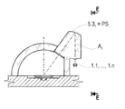
송신 장치에 관한 것으로, 바람직하게는 적어도 2개의 레이저 다이오드(1.1, ..., 1.n) 및 스캐닝 미러(2)를 포함하고, 상기 스캐닝 미러(2)는 그 중심(MP)에서 편향될 수 있고 투명한 커버 요소(4)를 갖는 하우징(3) 내에 배치되고; 상기 커버 요소(4)는, 적어도 커플링-아웃 영역(4.2)내에서, 곡률(K) 중심을 갖는 단일 중심 반구 쉘(HK)의 섹션에 의해서 형성되어 있고, 상기 반구 쉘(HK)의 곡률(K)의 상기 중심과 상기 스캐닝 미러(2)의 상기 중심(MP)이 일치하면서 상기 스캐닝 미러(2)를 커버하도록 배치되어 있고; 상기 커버 요소(4)는 커플링-인 영역내에서, 상기 레이저 빔(S1, ..., Sn)을 편향시키고 사전-시준하기 위하여, 실린더형 표면의 특별한 형태인 트로이드형 입구 표면(5.1) 및 적어도 하나의 토로이드형 출구 표면(5.21), 그들 사이에 배치되는 적어도 2개의 제1 미러 표면(5.31, 5.32)를 포함하는 송신 장치에 관한 것이다.It relates to a transmitting device, preferably comprising at least two laser diodes (1.1, ..., 1.n) and a scanning mirror (2), the scanning mirror (2) to be deflected at its center (MP) Is arranged in a housing 3 with a cover element 4 which is possible and transparent; The cover element 4 is formed by a section of a single central hemisphere shell HK having a center of curvature K, at least within the coupling-out region 4.2, and the curvature of the hemisphere shell HK. The center of (K) and the center (MP) of the scanning mirror (2) coincide and arranged to cover the scanning mirror (2); The cover element 4 is a special type of cylindrical surface, a toroidal inlet surface 5.1, to deflect and pre-collimate the laser beams S1, ..., Sn, within a coupling-in area. And at least one toroidal exit surface (5.2 1 ), at least two first mirror surfaces (5.3 1 , 5.3 2 ) disposed therebetween.
Description
본 발명은 LIDAR 스캐너용 송신 장치에 관한 것으로, 특히 적어도 하나의 스캔 각도 범위를 스캔하기 위하여 시준된(collimated) 레이저 방사를 사용하는 LIDAR 스캐너용 송신 장치에 관한 것이다.The present invention relates to a transmission device for a LIDAR scanner, and more particularly to a transmission device for a LIDAR scanner that uses collimated laser radiation to scan at least one scan angle range.
거리 측정에서, 개별 스캔 포인트가 거의 무한대까지 이미징되고, 개별 스캔 각도 범위는 2 차원 스캔 필드를 스캐닝함으로써 3 차원 범위로 연장되거나 1 차원 스캔 라인을 스캐닝함으로써 2 차원 범위로 연장된다.In the distance measurement, individual scan points are imaged to almost infinity, and the individual scan angle range extends to the three-dimensional range by scanning the two-dimensional scan field or to the two-dimensional range by scanning the one-dimensional scan line.
스캔 필드 또는 스캔 라인의 연장은 스캔 미러의 최대 편향(deflection) 각도에 의해 제한되지만, 그 깊이는 이동한 거리에 따라 방사선의 세기가 기하급수적으로 감소하는 Beer-Lambert의 법칙에 의해 한편으론 결정되고, 또 다른 한편으론 방사선 소스의 출력을 제한하게 되는 요구되는 레이저 등급에 따라 결정된다.The extension of the scan field or scan line is limited by the maximum deflection angle of the scan mirror, but its depth is determined on the one hand by Beer-Lambert's law, where the intensity of the radiation decreases exponentially with the distance traveled On the other hand, it depends on the required laser class, which limits the output of the radiation source.
넓은 스캔 각도 범위는 예를 들어 넓은 공간 영역을 간섭없이 모니터링해야하는 분야가 관심의 대상이다. 이러한 응용 분야는 예를 들어 항공, 해운, 군사 기술 또는 도로 차량의 자율 주행이다.Wide scan angle ranges are of interest, for example, in areas where large spatial areas need to be monitored without interference. Such applications are, for example, autonomous driving in aviation, shipping, military technology or road vehicles.
넓은 스캔 각도가 커버될 수 있는 스캐닝 미러로써 회전 미러를 사용하는 경우, 이러한 미러 축을 마운트하려면 예를들어 홀더(브라킷)같은 추가적인 개별 부품이 필요하게 된다. 회전으로 발생되는 마찰로 인해 마모가 생기고 결과적으로 미끄러짐(슬립)이 발생된다. 또한, 개별 부품들로 이루어진 조립품은 제조하기에 오늘날 일반적으로 더 복잡하고, 그에 따라 일체화된(모놀리식) 조립품보다는 더 비싸고, 또한 소형화가 쉽지 않고 더 무겁게 되는 경향이 있다.When using a rotating mirror as a scanning mirror that can cover a wide scan angle, mounting these mirror axes requires additional individual parts, for example holders (brackets). Wear occurs due to friction caused by rotation, resulting in slip (slip). In addition, assemblies made up of individual parts are generally more complex today to manufacture, and thus tend to be more expensive than integrated (monolithic) assemblies, and also tend to be less compact and heavier.
유연 힌지(flexure hinge)를 통해 프레임에 모놀리식으로(일체화되어) 연결된 MEMS(micro-electro-mechanical system) 미러는 180 °서로에 대하여 오프셋되어 기계적으로 보여지는 회전 축을 형성하고 MEMS 미러의 중심에 배치된 2개의 조인트 힌지를 사용하여 완전히 마모없이 작동한다. 상업적으로 이용 가능한 MEMS 미러는 단순히 한개의 회전 축에 대하여, 서로 직교하는 2 개의 회전축에 대하여, 또는 개별 서스펜션을 형성하는 3 개 이상의 조인트에 대하여 편향될 수 있다. 프레임에 대한 MEMS 미러의 편향 각도는 조인트 힌지 연결로 인해 편향되지 않은 영점 위치에 대해 각각 약 +/- 10 °로 제한된다. 마찰없는 동작, 달성 가능한 높은 동작 주파수 및 상대적으로 저렴한 가격으로 MEMS 미러는 특히 역동적이고, 콤팩트하고, 견고한 디바이스용으로 매우 매력적이다.The micro-electro-mechanical system (MEMS) mirrors monolithically (integrated) connected to the frame via a flexible hinge are offset relative to each other by 180 ° to form a mechanically visible axis of rotation and to the center of the MEMS mirror. The two joint hinges are arranged to operate completely without wear. Commercially available MEMS mirrors can simply be deflected about one axis of rotation, about two axes of rotation orthogonal to each other, or about three or more joints forming separate suspensions. The deflection angle of the MEMS mirror with respect to the frame is limited to about +/- 10 °, respectively, for the zero-deflection position due to the joint hinge connection. With its frictionless operation, high achievable operating frequency and relatively low price, MEMS mirrors are particularly attractive for dynamic, compact and rugged devices.
그러나, LIDAR 스캐너의 송신 장치를 위한 스캐닝 미러로서 MEMS 미러를 사용하는 경우, 제한된 작은 편향 각은 불리하다. MEMS 미러를 통해 반사된 레이저 빔의 최대 스캔 각도 범위는 최대 편향 각도의 4 배이므로 최대 약 40 °이다. 개별 MEMS 미러의 스캔 각도 범위에서 더 큰 스캔 각도 범위를 얻거나 서로 이격 된 여러 스캔 각도 범위를 제공하기 위해 여러 MEMS 미러를 사용하려는 것은 자명할 것이다. 그러나 이것은 한편으로는 장치의 컴팩트화하는데 절충할 수 밖에 없을 것이고, 다른 한편으로는 MEMS 미러들의 움직임을 동기화시키기 위한 기술적 조치가 취해져야한다. 그 대신에, 큰 스캔 각도 범위를 형성하기 위해 함께 결합되는 복수의 인접한 개별 스캔 각도 범위를 스캔하기 위해, 복수의 레이저 빔을 상이한 입사각으로 MEMS 미러 상으로 지향시키는 것은, MEMS 미러의 전면 위에 있는 커버 요소가, 종래 기술에 따르면 커버 요소는 평면판의 형태로만 알려져 있으므로, 복수의 개별 레이저 빔들에게 다르게 영향을 주게되므로, 그러한 단점을 갖게 될 것이다. 이에 더하여, 각 레이저 빔은 상기 빔 방향에서 하방(downstream)에 배치되는 콜리메이터를 갖는 레이저 빔 소스가 요구되고, 이러한 상기 레이저 빔 소소는, 각 레이저 빔이 상기 MEMS 미러 상에서 소정의 다른 입사각으로 부딪히도록(impinge), 각 빔 방향에서 서로간에 배열되어야만 한다.However, when using a MEMS mirror as a scanning mirror for a transmission device of a LIDAR scanner, the limited small deflection angle is disadvantageous. The maximum scan angle range of the laser beam reflected through the MEMS mirror is 4 times the maximum deflection angle, so it is up to about 40 °. It would be obvious to try to use multiple MEMS mirrors to obtain larger scan angle ranges from the scan angle ranges of individual MEMS mirrors or to provide multiple scan angle ranges spaced apart from each other. On the one hand, however, it will have to compromise on the compactness of the device, and on the other hand, technical measures must be taken to synchronize the movement of the MEMS mirrors. Instead, directing a plurality of laser beams onto the MEMS mirror at different angles of incidence to scan a plurality of adjacent individual scan angle ranges that are joined together to form a large scan angle range covers the front of the MEMS mirror. Since the element is known only in the form of a flat plate according to the prior art, it will have such drawbacks because it affects a plurality of individual laser beams differently. In addition, each laser beam requires a laser beam source having a collimator disposed downstream in the beam direction, and such laser beam source is such that each laser beam strikes at a predetermined different angle of incidence on the MEMS mirror. Impinge, must be arranged in each beam direction to each other.
스캐닝 미러가 MEMS 미러인지에 상관없이, 스캐닝 미러가 하우징에 수용되고 커버로 덮여서 보호되는 이유가 있을 수 있다. 알려진 바와 같이, 커버 요소는 편향되지 않은 미러에 평행하게 또는 경사지게 배열된 항상 투명한 평면판이다.Regardless of whether the scanning mirror is a MEMS mirror, there may be a reason why the scanning mirror is accommodated in a housing and covered with a cover to protect it. As is known, the cover element is always a transparent flat plate arranged parallel or inclined to an unbiased mirror.
커버 요소에 부딪히는 레이저 빔은, 상기 스캐닝 미러로 향하는 또한 복수의 레이저 빔에 영향을 줄 수 있고, 스캐닝 미러상에서 반사된 복수의 레이저 빔 각각은 결과적으로 상기 평면판상의 입사 각도에 따라 프레넬(Fresnel) 손실이 다소 발생하고, 그 위치에 따라 상기 레이저 빔의 세기를 다소 감소시키게 된다. 또한, 커버 요소상에서 바람직하지 않은 반사가 일어날 수 있다.The laser beam striking the cover element may also affect a plurality of laser beams directed to the scanning mirror, each of the plurality of laser beams reflected on the scanning mirror consequently depending on the angle of incidence on the flat plate Fresnel ) Some loss occurs, and the intensity of the laser beam is slightly reduced depending on the position. In addition, undesirable reflections may occur on the cover element.
DE 10 2012 025 281 A1은 레이저 빔을 방출하기위한 송신 유니트를 갖는 광학 물체 검출 유닛을 개시하고, 상기 송신 유니트는 레이저 빔을 방출하기 위한 송신기, 하나 또는 두 개의 피봇 방향으로 중심에서 피봇될 수 있는 마이크로미러, 상기 전송 빔 경로(패쓰)에서 상기 마이크로미러 이후에(지나서) 배치되는, 마이크로미러를 덮고 있는 트랜스미터 렌즈를 포함하고 있다. 메니스커스(meniscus) 렌즈로 설계된 상기 트랜스미터 렌즈는 여기서 송신 유닛의 하우징을 위한 커버로서 기능할 수도 있다. 여기서의 단점은 레이저 빔이 트랜스미터 렌즈를 통해(지나서) 마이크로 미러로 향하여 가이드될 수 없기 때문에 마이크로미러가 자체적으로 하우징될 수 없다는 것이다.DE 10 2012 025 281 A1 discloses an optical object detection unit having a transmission unit for emitting a laser beam, the transmission unit being a transmitter for emitting a laser beam, which can be pivoted centrally in one or two pivot directions It includes a micromirror, a transmitter lens covering the micromirror, disposed (after) the micromirror in the transmission beam path (path). The transmitter lens, designed as a meniscus lens, here may also function as a cover for the housing of the transmission unit. The disadvantage here is that the micromirror cannot be housed on its own because the laser beam cannot be guided through the transmitter lens towards the micromirror.
DE 10 2011 006 159 A1은 적어도 2 개의 스위칭 위치로 스위블될 수 있고, 그래디언트(gradient) 인덱스 렌즈로 덮인 MEMS 미러를 포함하는 프로젝션 장치를 개시하고 있다. 상기 그래디언트 인덱스 렌즈는 상기 MEM 미러를 마주보는 평면 표면(planar surface)을 갖는 평면-볼록(plano-convex) 렌즈이다. 상기 그래디언트 인덱스 렌즈를 통해 입사되는 아마도 평행한 레이저 빔은 MEMS 미러에 초점을 맞추고, 반사 후 그래디언트 인덱스 렌즈를 다시 통과할 때 필요한 경우 다시 시준(collimated)된다. 하나의 단점은 상기 MEMS 미러는 그라디언트 인덱스 렌즈의 평면 표면에 의해 제한되어, 매우 작은 스위블 범위를 가지며, 또 다른 단점은 다른 입사각으로 들어올 수 있는 레이저 빔은, 상기 그래디언트 인덱스 렌즈의 평면 표면에서의 굴절때문에, MEMS 미러상의 동일한 지점에 부딪히지 않는다는 것이다.DE 10 2011 006 159 A1 discloses a projection device comprising a MEMS mirror that can be swiveled to at least two switching positions and covered with a gradient index lens. The gradient index lens is a plano-convex lens having a planar surface facing the MEM mirror. A possibly parallel laser beam incident through the gradient index lens focuses on the MEMS mirror and collimates again if necessary when passing back through the gradient index lens after reflection. One disadvantage is that the MEMS mirror is limited by the planar surface of the gradient index lens, so it has a very small swivel range, and another disadvantage is that the laser beam, which can enter at different angles of incidence, refracts on the plane surface of the gradient index lens. Therefore, it does not hit the same point on the MEMS mirror.
본 발명의 목적은 커버 요소에 의해 보호되는 스캐닝 미러를 포함하는 LIDAR 스캐너를 위한 송신 장치를 제공하는 것이며, 특히, 낮은 프레넬 손실(있는 경우) 만 있고, 바람직하지 않은 반사는 커버 요소에서 발생하지 않는 LIDAR 스캐너용 송신 장치를 제공하는 것이다. 이에 더하여, 본 발명의 목적은 컴팩트한 디자인을 갖으면서 생산시 조정이 거의 필요없는 송신 장치를 제공하는 것이다.It is an object of the present invention to provide a transmission device for a LIDAR scanner comprising a scanning mirror protected by a cover element, in particular only with low Fresnel losses (if any) and undesirable reflections do not occur in the cover element. It is to provide a transmission device for a LIDAR scanner. In addition, the object of the present invention is to provide a transmission device having a compact design and requiring little adjustment during production.
본 발명의 목적은 청구항 1에 기재된 기술적 특징에 의해 달성된다. 유리한 실시예는 청구항 1을 인용하는 종속항에 기재되어 있다.The object of the present invention is achieved by the technical features described in claim 1. Advantageous embodiments are described in the dependent claims citing claim 1.
본 발명은 예시적인 실시예들 및 도면들을 참조하여 아래에서 더 상세히 설명될 것이다.The invention will be described in more detail below with reference to exemplary embodiments and figures.
도 1a - 1c는 송신 장치의 제1 실시예를 도시한 개략도이다.
도 2a - 2b는 송신 장치의 제2 실시예를 도시한 개략도이다.
도 3a - 3b는 송신 장치의 제3 실시예를 도시한 개략도이다.
도 4는 송신 장치의 제2 실시예의 디자인의 사시도이다.
도 5는 송신 장치의 제3 실시예의 디자인의 사시도이다.1A-1C are schematic diagrams showing a first embodiment of a transmitting device.
2A-2B are schematic diagrams showing a second embodiment of the transmitting device.
3A to 3B are schematic diagrams showing a third embodiment of the transmission device.
4 is a perspective view of the design of the second embodiment of the transmitting device.
5 is a perspective view of the design of the third embodiment of the transmission device.
본 발명에 따르는 송신 장치는, 도 1a 내지 도 1c의 예제에 도시된 바와 같이 모든 실시예들에서 하나의 레이저 다이오드(1.1) 또는 적어도 2개의 레이저 다이오드(1.1, ..., 1.n)를 포함하고 있고, 각각은 빔 축(A1, ..., An)을 갖고, 빠른 축(fa, fast axis) 및 늦은 축(sa, slow axis)에서 다른 방사 각을 갖고 레이저 빔(S1, ..., Sn)을 방출한다(emit). 상기 송신 장치가 적어도 2개의 레이저 다이오드(1.1, ..., 1.n)를 포함하고 있는 경우에, 그들은 일렬로 형성되고 늦은 축의 방향에서 옆으로 배치되고, 상기 빔 축(A1, ..., An)은 서로 간에 평행하다. 빔 축이 서로 간에 각을 이루는 배치와 비교하면, 상기 빔 축이 함께 가까이 배치될 수 있고 소정의 각도 위치를 정해기 위해서 이동하는 조정이 필요없게 된다.The transmitting device according to the present invention, as shown in the example of Figure 1a to Figure 1c in one embodiment, one laser diode (1.1) or at least two laser diodes (1.1, ..., 1.n) And each has a beam axis (A1, ..., An), a fast axis (fa, fast axis) and a slow axis (sa, slow axis) with different radiation angles and laser beams (S1, .. ., Sn) (emit). When the transmitting device includes at least two laser diodes (1.1, ..., 1.n), they are formed in a line and arranged laterally in the direction of the late axis, and the beam axes (A1, ... , An) are parallel to each other. Compared to an arrangement in which the beam axes are angled to each other, the beam axes can be placed close together and no adjustment is required to move to determine a predetermined angular position.
더구나, 상기 송신 장치는 스캐닝 미러(2)를 포함하고, 상기 스캐닝 미러는 그 중심(MO)에서 반사될 수 있고, 투명한 커버 요소(4)를 갖는 하우징(3)내에 배치된다. 상기 적어도 하나의 레이저 빔 S1, ... Sn의 상기 빔 축 A1, ..., An은, 상기 적어도 하나의 레이저 빔 S1, ... Sn이 커플링-인 영역(4.1)내의 상기 커버 요소(4)를 통과하여 상기 스캐닝 미러(2)의 상기 중심(MP)상에 부딪히도록(impinge), 상기 커버 요소(4)로 향해져 있다. 상기 적어도 하나의 레이저 빔 S1, ... Sn이 상기 스캐닝 미러(2)에서 반사된 후에 커플링-아웃 영역(4.2)내의 상기 커버 요소(4)를 다시 통과하게 된다.Moreover, the transmitting device comprises a
본 발명에서는, 필수적으로, 상기 커버 요소(4)는, 상기 적어도 하나의 레이저 빔(S1, ..., Sn)을 상기 빠른 축 방향으로 사전-시준하기(pre-collimating) 위해서 커플링-인(coupling-in) 영역(4.1)에서 토로이드형(toroidal) 입구 표면(5.1)을 갖고; 상기 적어도 2개의 레이저 빔(S1, ..., Sn)을 상기 중심(MP)으로 편향시키기 위하여 상기 적어도 2개의 레이저 다이오드(1.1, ..., 1.n)에 할당되는 각각의 제1 미러 표면(5.31, ..., 5.3n)을 갖고; 상기 적어도 하나의 레이저 빔(S1, ..., Sn)를 상기 늦은 축(sa) 방향으로 사진-시준하기 위해서 적어도 하나의 트로이드형 출구 표면(5.21, ..., 5.2n)을 갖는다. 여기서 트로이드형 표면이란 2차원 평면 형상(planar figure)을 그 형상과 동일한 평면에서의 회전축을 중심으로 상기 평면 형상을 회전시켜 기하학적으로 만들어질 수 있는 입체의 표면 또는 표면의 섹션으로 이해될 것이다. 토이드의 중요한 특별한 경우 또는 제한된 경우로 토로스(도넛형), 구, 회전 실린더 뿐만 아니라 파라볼릭(포물선형) 단면을 갖는 실린더가 있다. 이미지 에러를 교정하기 위하여 상기 표면을 약간 변경하는 것은 이 분야의 통상의 기술자에게 흔한 일이다.In the present invention, essentially, the cover element 4 is coupled-in to pre-collimate the at least one laser beam S1, ..., Sn in the fast axial direction. has a toroidal inlet surface 5.1 in the (coupling-in) region 4.1; Each first mirror assigned to the at least two laser diodes (1.1, ..., 1.n) to deflect the at least two laser beams (S1, ..., Sn) to the center (MP) Has a surface (5.3 1 , ..., 5.3 n ); It has at least one toroidal exit surface (5.2 1 , ..., 5.2 n ) for photo-collimating the at least one laser beam (S1, ..., Sn) in the direction of the slow axis (sa). Here, the toroidal surface will be understood as a three-dimensional surface or a section of a surface that can be geometrically made by rotating the two-dimensional planar figure around the axis of rotation in the same plane as the shape. An important special case or limited case of a toroid is a torus (donut), spherical, rotating cylinder as well as a cylinder with a parabolic (parabolic) cross section. It is common for a person skilled in the art to slightly alter the surface to correct image errors.
토로이드형 (굴절하는 또는 반사하는) 광학적 표면은 일반적으로 두개의 상호 수직한 방향에서 빔 형태(beam shape)에 다르게 영향을 준다. 실린더형 렌즈(단면의 형태가 구 모양일 필요는 없다)의 특별하고 제한된 경우에는, 상기 빔 형태는 한 방향에서 영향을 받지 않는다. 통상적인 구형의 렌즈의 특별하고 제한된 경우에는 양 방향에서 동일하게 영향을 받는다.Toroidal (refractive or reflective) optical surfaces generally affect the beam shape differently in two mutually perpendicular directions. In the special and limited case of a cylindrical lens (the shape of the cross section need not be spherical), the beam shape is not affected in one direction. The special and limited case of a conventional spherical lens is equally affected in both directions.
본 발명에서는, 필수적으로, 상기 커버 요소(4)가 상기 커플링-아웃(coupling-out) 영역(4.2)내에서 적어도 단일 중심 반구 쉘(monocentric hemisphere shell)(HK)(이하에서는 단순히 반구 쉘(HK)이라고 칭한다)의 섹선으로 형성되고, 상기 반구 쉘(HK)의 곡률(K) 중심과 상기 스캐닝 미러(2)의 상기 중심(MP)이 일치하도록, 상기 스캐닝 미러(2)를 보호하도록 배치된다. 단일 중심(Monocentric)은 상기 반구 쉘(HK)의 두개의 표면의 곡률 중심을 뜻한다. 생산 및 조립 관련 허용 오차, 곡률(K)의 중심과 상기 중심(MP)사이의 허용 편차뿐만 아니라 장기간의 드리프트는 빔 질을 저하시키지만, 한계 범위내에서 허용될 수 있다.In the present invention, essentially, the cover element 4 is at least a monocentric hemisphere shell (HK) within the coupling-out region 4.2 (hereinafter simply a hemisphere shell ( HK), and arranged to protect the
입사각(α1, ..., αn)에 완전히 독립적이고, 그러한 입사각에서 적어도 하나의 레이저 빔(S1, ..., Sn)은 편향되지 않은 스캐닝 미러(4)의 수직선(L)에 대하여 스캐닝 미러(4)상에 부딪히고(impinge), 상기 빔 축(A1, ..., An)은, 상기 스캐닝 미러(4)상의 반사 후, 반사하는 동안에 그 위치에 상관없이, 상기 커플링-아웃 영역(4.2)에 형성된 사익 반구 쉘(HK)의 섹션에 항상 수직적으로 부딪힌다. It is completely independent of the incidence angles α1, ..., αn, and at such an incident angle, at least one laser beam S1, ..., Sn is a scanning mirror with respect to the vertical line L of the unbiased scanning mirror 4 (4) Impinge on the image, and the beam axes A1, ..., An, after the reflection on the scanning mirror 4, regardless of its position during reflection, the coupling-out area The section of the Sik Hemispherical Shell (HK) formed in (4.2) is always hit vertically.
상기 커버 요소에 부딪히는 상기 레이저 빔(S1, ..., Sn)이 상기 커플링-인 영역(4.1)내의 상기 커버 요소(4)를 통과할 때, 한편으론 반사되고 또 다른 한편으론, 상기 레이저 다이오드(1.1, ..., 1.n)의 상기 빠른 축(fa) 및 늦은 축(sa) 방향으로 사전-시준(pre-collimated)되는데, 여기서, 상기 레이저 빔을 사전-시준하는 것은 상기 레이저 빔이 상기 빠른 축(fa) 및 상기 늦은 축(sa) 방향으로 동일한 작은 수렴각(convergence angle)으로 상기 스캐닝 미러(2)의 상기 중심(MP)에 부딪히고, 상기 커플링-아웃 영역(4.2)내에서 상기 커버 요소를 통과한 후에 충분히 시준(fully collimated)되도록 하기 위한 것이다.When the laser beams S1, ..., Sn striking the cover element pass through the cover element 4 in the coupling-in area 4.1, on the one hand they are reflected and, on the other hand, the laser Pre-collimated in the direction of the fast axis (fa) and late axis (sa) of the diodes (1.1, ..., 1.n), wherein pre-collimating the laser beam is the laser The beam hits the center MP of the
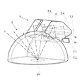
유리하게, 상기 커버 요소(4)는, 도 4에 도시된 바와 같이, 쉘(6) 및 광학 블록(5)에 의해서 형성된다. 상기 커버 요소(4)는, 또한 유리하게, 도 5에 도시된 바와 같이, 쉘(6) 및 이웃하는 광학 블록(5)에 의해서 형성될 수 있다. 이러한 경우에, 상기 반구 쉘(HK)의 섹션은 쉘(6)에 형성되고, 상기 토로이드형 입구 표면(5.1), 상기 적어도 2개의 제1 미러 표면(5.31, ..., 5.3n), 및 상기 적어도 하나의 토로이드형 출구 표면(5.21, ..., 5.2n)은 상기 광학 블록(5)에 형성된다. 상기 쉘(6)은 유리하게 상기 반구 쉘(HK)의 일 부분을 구성한다.Advantageously, the cover element 4 is formed by a shell 6 and an
도 1a 내지 1c는, 하나의 예제로, 제1 실시예를 도시하고, 제1 실시예는, 레이저 다이오드(1.2)에 의해서 방출되는 레이저 빔(S2) 및 레이저 다이오드(1.1. 1.2, 1.3)의 빔 축(A1, A2, A3)을 포함하는 3개의 레이저 다이오드(1.1, 1.2, 1.3)를 포함하고 있다. 상기 레이저 빔(S1, S2, S3)은 상기 빠른 축(fa)의 방향에서 상기 토로이드형 입구 표면(5.11)에서 굴절에 의해서 사전-시준된다. 여기서, 상기 토로이드형 입구 표면(5.11)는 실린더형 표면을 나타낸다.1A to 1C show, as an example, the first embodiment, and the first embodiment of the laser beam S2 and the laser diodes 1.1.1.2 and 1.3 emitted by the laser diode 1.2. It contains three laser diodes (1.1, 1.2, 1.3) that include beam axes (A1, A2, A3). The laser beams S1, S2, S3 are pre-collimated by refraction at the toroidal inlet surface 5.11 in the direction of the fast axis fa. Here, the toroidal inlet surface 5.11 represents a cylindrical surface.
제1 미러 표면(5.31, 5.32, 5.33)의 현재의 개수는 레이저 빔(S1, S2, S3)의 현재의 개수와 동일하다. 제1 미러 표면(5.31, 5.32, 5.33)은 평면의 표면으로 서로 경사져 있고, 그것의 크기 및 중심간의 거리뿐만 아니라 이웃하는 평면간의 경사각은 상기 레이저 다이오드(1.1, 1.2, 1.3)의 거리에 의해서 결정된다. 상기 3개의 레이저 빔 중 가운데 빔(S2)는 상기 빠른 축(fa)를 포함하는 평면에서 단지 편향되고, 그 밖의 레이저 빔(S1, S3)은 또한, 그것에 수직인 평면에서 편향되어, 3개의 모든 레이저 빔(S1, S2, S3)는 상기 스캐닝 미러(2)의 중심(MP)에 부딪히게 된다. 상기 제1 미러 표면(5.31, 5.32, 5.33)은 상기 레이저 빔(S1, S2, S3)의 시준(collimation)에 영향을 주지 않는다. 제1 미러 표면(5.31, 5.32, 5.33)의 각각은 토로이드형 출구 표면(5.21, ..., 5.2n)에 할당된다. 상기 토로이드형 출구 표면(5.21, ..., 5.2n) 각각은, 상기 입구 표면(5.1)이 낮은 굴절력을 갖을 수 있도록, 실린더형 표면일 수 있고, 그에 따라 늦은 축(sa)의 방향으로만 시준된다. 구형 표면은, 상기 빠른 축(fa) 방향으로 상기 레이저 빔(S1, S2, S3)의 빔 각(beam angle)이 상기 토로이드형 입구 표면(5.1)에서 상기 레이저 빔(S1, S2, S3)의 사전-시준에 의해서 상기 늦은 축(sa) 방향으로 상기 빔 각이 이미 맞추어 적응되었다면, 유리하게 이런 목적으로 제공될 수 있다. 상기 사전-시준된 레이저 빔(S1, S2, S3)은, 음의 굴절력을 갖는 상기 커플링-아웃 영역(4.2)에서 상기 굴절에 의해서 완전히 시준되기 위해서는 약각 수렴적이어야 한다.The current number of first mirror surfaces (5.3 1 , 5.3 2 , 5.3 3 ) is the same as the current number of laser beams S1, S2, S3. The first mirror surfaces (5.3 1 , 5.3 2 , 5.3 3 ) are inclined to each other with a flat surface, and the size and distance between the centers as well as the inclination angle between neighboring planes are the distances of the laser diodes (1.1, 1.2, 1.3) It is decided by. Of the three laser beams, the middle beam S2 is only deflected in the plane containing the fast axis fa, and the other laser beams S1 and S3 are also deflected in the plane perpendicular to it, all three The laser beams S1, S2, and S3 collide with the center MP of the
도 2a 및 도 2b에서 도시된 제2 실시예는, 상기 커플링-인 영역(4.1)에서 제2 미러 표면(5.4)이 있다는 점에서, 제1 실시예와 다르다. 상기 제2 미러 표면(5.4)는, 필요한 공간을 최소화하고, 입구 표면(5.1) 및 레이저 다이오드(1.1, 1.2, 1.3)의 위치를 변화시킬 수 있도록 상기 레이저 빔(S1, S2, S3)을 굽히는 역할만 한다.The second embodiment shown in FIGS. 2A and 2B differs from the first embodiment in that there is a second mirror surface 5.4 in the coupling-in area 4.1. The second mirror surface 5.4 bends the laser beams S1, S2, S3 to minimize the required space and to change the positions of the inlet surface 5.1 and the laser diodes 1.1, 1.2, 1.3. It plays only a role.
도 4는 제2 실시예의 디자인에 대한 사시도를 도시한다. 상기 커버 요소(4)의 모양은 필요한 공간을 최소화시키기 위하여, 커플링-인 영역 및 커플링-아웃 영역(4.1, 4.2) 바깥에서 맞추어 적응되어 있다는 것은 분명하게 나타나 있다.4 shows a perspective view of the design of the second embodiment. It is evident that the shape of the cover element 4 is adapted to fit outside the coupling-in and coupling-out areas 4.1 and 4.2 in order to minimize the required space.
도 3a 및 3b에 도시된 제3 실시예는, 많은 개수의 레이저 다이오드(1.1, ..., 1.n)가 있는 경우이거나 상기 빔 축(A1, ..., An) 사이의 거리가 정해져 있는 경우에 특별히 유리하다. 레이저 다이오드(1.1, ..., 1.n)와 같은 개수의 제1 미러 표면(5.31, ..., 5.3n)을 갖는 대신에, 여기서는 단지 하나의 제1 미러 표면(5.31)을 갖는다. 상기 제1 미러 표면은 초첨(Fps)를 갖는 포물선모양의 미러 표면(PS)을 갖고, 상기 초점(Fps)이 곡률(K)의 중심 및 중심(MP)과 일치하도록 배치되고, 이 경우에, 하나의 토로이드형 출구 표면(5.21)이 하방으로 배치되는 경우에는 그 토로이드형 출구 표면의 굴절력은 이론적으로 무시된다. 상기 레이저 다이오드(1.1, ..., 1.n) 사이의 거리, 즉 상기 빔 축(A1, ..., An)사이의 거리에 상관없이, 상기 빔 축(A1, ..., An)은 상기 초점(Fps)로 반사되어 지고, 따라서 상기 스캐닝 미러(2)의 중심(MP)으로 반사되게 된다. 상기 포물선 형상의 미러 표면(PS)는 토로이드형 포물선 형상의 미러 표면일 수 있고, 그에 의해서 엄밀히 말하면 촛점선(focal line)을 만들게 되고, 그러나 그것은 모든 빔 축(A1, ..., An)이 만나는 한 점을 포함하게 되고, 촛점(Fps)으로 이해되어야 한다.3A and 3B, in the case of a large number of laser diodes (1.1, ..., 1.n) or the distance between the beam axes (A1, ..., An) is determined It is particularly advantageous if present. Instead of having the same number of first mirror surfaces (5.3 1 , ..., 5.3 n ) as the laser diodes (1.1, ..., 1.n), here only one first mirror surface (5.3 1 ) Have The first mirror surface has a parabolic mirror surface PS having a focal point Fps, and the focal point Fps is arranged to coincide with the center and the center MP of the curvature K, in this case, When one toroidal outlet surface 5.2 1 is disposed downward, the refractive power of the toroidal outlet surface is theoretically neglected. Regardless of the distance between the laser diodes (1.1, ..., 1.n), that is, the distance between the beam axes (A1, ..., An), the beam axis (A1, ..., An) Is reflected at the focal point Fps, and thus is reflected at the center MP of the
상기 하나의 토로이드형 출구 표면(5.21)은, 이런 경우에, 비구형 실린더형 표면이고, 상기 입구 표면(5.1) 및 상기 하나의 출구 표면(5.21)의 실린더 축은 서로 직교하게 된다.The one toroidal outlet surface 5.2 1 is, in this case, a non-spherical cylindrical surface, and the cylinder axes of the inlet surface 5.1 and the one outlet surface 5.2 1 are orthogonal to each other.
상기 쉘(6) 및 상기 광학 블록(5)는 개별적으로 제조되고, 서로 연결되고, 바람직하게는 접착에 의해서 연결될 수 있다. 그러나, 그들이 하나의 부품으로 일체화되어(moonolithically) 제조되면 유리하다.The shell 6 and the
상기 도면들에 도시되지 않은 특별한 경우는 단지 하나의 레이저 다이오드(1.1)만으로 된 송신 장치이다. 이런 경우에는 제1의 미러 표면(5.31)은, 상기 단지 하나의 레이저 빔(S1)의 상기 하나의 빔 축(A1)은 상기 스캐닝 미러(2)의 중심(MP)로 곧바로 향할 수 있기 때문에, 필요없다. 그러면, 상기 커플링-인 영역(4.1)에서 단지 상기 입구 표면(5.1) 및 하나의 출구 표면(5.21)를 거쳐 단지 가이드된다.A special case not shown in the above figures is a transmitting device with only one laser diode 1.1. In this case, since the first mirror surface 5.3 1 , the one beam axis A1 of the only one laser beam S1 can be directed directly to the center MP of the
본 발명에 따르는 송신 장치의 모든 실시예들은 시준하기 위한 모든 빔의 모양이 형성되는(shaping) 것 및 상기 스캐닝 미러(2) 쪽으로 레이저 다이오드 빔(S1, ..., Sn)이 빔 편향되는 것이 상기 커버 요소(4) 내에서 이루어지므로, 따라서, 컴팩트하고, 저-조정(low-adjustment) 디자인을 제공하는 이점을 갖는다.All embodiments of the transmitting apparatus according to the present invention are that all beam shapes for collimation are formed and that the laser diode beams S1, ..., Sn are deflected toward the
참조 부호 리스트
1.1, ..., 1.n
레이저 다이오드
2
스캐닝 미러
3
하우징
4
커버 요소
4.1
(커버 요소(4)의)커플링-인 영역(coupling-in region)
4.2
(커버 요소(5)의)커플링-아웃 영역(coupling-out region)
5
광학 블럭
5.1
(광학 블럭(5)의) 입구 표면
5.21, ..., 5.2n
(광학 블럭(5)의) 출구 표면
5.31, ..., 5.3n
(광학 블럭(5)의) 제1 미러 표면
5.4
(광학 블럭(5)의) 제2 미러 표면
6
쉘
S1, ..., Sn
레이저 빔
A1, ..., An
(레이저 빔(S1, ..., Sn)의) 빔 축
fa
(레이저 다이오드(1.1, ..., 1.n)의) 빠른 축(fast axis)
sa
(레이저 다이오드(1.1, ..., 1.n)의) 늦은 축(slow axis)
MP
(스캐닝 미러(2)의) 중심
L
수직인(perpendicular)
HK
단일 중심 반구 쉘
PS
포물선 형상의 미러 표면
Fps
포물선 형상의 미러 표면의 촛점
α1, ..., αn
입사각List of reference signs
1.1, ..., 1.n laser diode
2 scanning mirror
3 housing
4 cover elements
4.1 Coupling-in region (of cover element 4)
4.2 Coupling-out region (of cover element 5)
5 optical blocks
5.1 Entrance surface (of optical block 5)
5.2 1 , ..., 5.2 n (of optical block (5)) exit surface
5.3 1 , ..., 5.3 n 1st mirror surface (of optical block 5)
5.4 Second mirror surface (of optical block 5)
6 shell
S1, ..., Sn laser beam
A1, ..., An beam axis (of laser beams S1, ..., Sn)
fa fast axis (of laser diodes (1.1, ..., 1.n))
sa (of laser diodes (1.1, ..., 1.n)) slow axis
MP (of the scanning mirror (2)) center
L vertical (perpendicular)
HK single center hemisphere shell
PS parabolic mirror surface
Fps parabolic mirror focus
α1, ..., αn angle of incidence
Claims (8)
상기 송신 장치는 하나의 레이저 다이오드(1.1) 또는 적어도 2개의 레이저 다이오드(1.1, ..., 1.n) 및 스캐닝 미러(2)를 포함하고,
상기 레이저 다이오드 각각은 빔 축(A1, ..., An)을 갖고, 빠른 축(fa) 및 늦은 축(sa)에서 다른 방사 각을 갖는 레이저 빔(S1, ..., Sn)을 방출하고, 상기 적어도 2개의 레이저 다이오드(1.1, ..., 1.n)는 각각의 늦은 축(sa) 방향으로, 일렬로 형성되어, 나란히 배치되고, 상기 빔 축(A1, ..., An)은 서로간에 평행하게 배치되고,
상기 스캐닝 미러(2)는 그 중심(MP)에서 편향될 수 있고, 투명한 커버 요소(4)를 갖는 하우징(3) 안쪽에 배열되고; 상기 적어도 하나의 레이저 빔(S1, ..., Sn)의 상기 빔 축(A1, ..., An)은, 상기 적어도 하나의 레이저 빔(S1, ..., Sn)이 커플링-인 영역(4.1)내 상기 커버 요소(4)를 통과한 후에, 상기 중심(MP)에 부딪히도록, 상기 커버 요소(4)로 향하고; 상기 적어도 하나의 레이저 빔(S1, ..., Sn)은, 상기 스캐닝 미러(2)에서 반사된 후에, 커플링-아웃 영역(4.2)내에서 상기 커버 요소(4)를 다시 통과하는 송신 장치로서,
상기 커버 요소(4)는, 상기 빠른 축(fa) 방향으로 상기 적어도 하나의 레이저 빔(S1, ..., Sn)을 사전-시준하기 위하여, 상기 커플링-인 영역(4.1)에서, 토로이드형 입구 표면(5.1)을 갖고; 상기 커버 요소(4)는 상기 레이저 빔(S1, ..., Sn)을 상기 중심(MP)으로 편향시키기 위하여 상기 적어도 2개의 레이저 다이오드(1.1, ..., 1.n)에 할당된 각각의 제1 미러 표면(5.31, ..., 5.3n)을 갖고; 상기 커버 요소(4)는 곡률(K)의 중심을 갖는 단일 중심 반구 쉘(HK)의 섹션에 의해서 상기 커플링-아웃 영역(4.2)에 형성되고, 상기 커버 요소(4)는 곡률(K)의 상기 중심과 상기 스캐닝 미러의 상기 중심(MP)이 일치하면서 상기 스캐닝 미러(2)를 커버하도록 배치되는 것을 특징으로 하는 송신 장치.It is a transmitting device,
The transmitting device comprises one laser diode (1.1) or at least two laser diodes (1.1, ..., 1.n) and a scanning mirror (2),
Each of the laser diodes has a beam axis (A1, ..., An), emits a laser beam (S1, ..., Sn) having a different radiation angle in the fast axis (fa) and the slow axis (sa) and , The at least two laser diodes (1.1, ..., 1.n) are formed in a line in the direction of each of the late axis (sa), are arranged side by side, the beam axis (A1, ..., An) Are arranged parallel to each other,
The scanning mirror 2 can be deflected at its center MP and is arranged inside the housing 3 with a transparent cover element 4; The beam axes A1, ..., An of the at least one laser beam S1, ..., Sn have a coupling-in of the at least one laser beam S1, ..., Sn. After passing through the cover element 4 in the region 4.1, it is directed to the cover element 4 so as to hit the center MP; The transmitting device, after the at least one laser beam (S1, ..., Sn) is reflected from the scanning mirror (2), passes through the cover element (4) again in the coupling-out area (4.2). as,
The cover element 4 is in the coupling-in area 4.1 to pre-collimate the at least one laser beam S1, ..., Sn in the direction of the fast axis fa. Has an Lloyd-shaped entrance surface (5.1); The cover elements 4 are respectively assigned to the at least two laser diodes 1.1, ..., 1.n to deflect the laser beams S1, ..., Sn to the center MP. Has a first mirror surface of (5.3 1 , ..., 5.3 n ); The cover element 4 is formed in the coupling-out region 4.2 by a section of a single central hemisphere shell HK having a center of curvature K, and the cover element 4 is curvature K And the center of the scanning mirror and the center of the scanning mirror coincide with the scanning mirror 2.
상기 커버 요소(4)는 일체화되거나 이웃하게 되는 쉘(6) 및 광학 블럭(5)에 의해서 형성되고, 상기 단일 중심 반구 쉘(HK)의 상기 섹션은 상기 쉘(6) 및 상기 토로이드형 입구 표면(5.1) 상에 형성되고, 상기 적어도 하나의 제1 미러 표면(5.21, ..., 5.2n) 및 상기 적어도 하나의 토로이드형 출구 표면(5.21, ..., 5.2n)은 상기 광학 블럭(5)상에 형성되는 것을 특징으로 하는 송신 장치.According to claim 1,
The cover element 4 is formed by an integrated or neighboring shell 6 and an optical block 5, wherein the section of the single central hemisphere shell HK comprises the shell 6 and the toroidal inlet. Formed on the surface (5.1), the at least one first mirror surface (5.2 1 , ..., 5.2 n ) and the at least one toroidal exit surface (5.2 1 , ..., 5.2 n ) are A transmission device formed on the optical block (5).
상기 쉘(6)은 상기 단일 중심 반구 쉘(HK)의 일 부분을 구성하는 것을 특징으로 하는 송신 장치.According to claim 1,
The shell (6) constitutes a part of the single central hemisphere shell (HK) transmission device.
상기 송신 장치는 적어도 2개의 레이저 다이오드(1.1, ..., 1.n)을 포함하고, 상기 제1 미러 표면(5.31, ..., 5.3n)은, 상기 적어도 2개의 레이저 빔(S1, ..., Sn)이 다른 각도로 편향되도록, 서로 간에 경사져 있는 평면의 표면인 것을 특징으로 하는 송신 장치.The method according to any one of claims 1 to 3,
The transmitting device includes at least two laser diodes (1.1, ..., 1.n), the first mirror surface (5.3 1 , ..., 5.3 n ), the at least two laser beams (S1) , ..., Sn), the transmission device, characterized in that the surface of the plane inclined with respect to each other, so as to deflect at different angles.
상기 송신 장치는 적어도 2개의 레이저 다이오드(1.1, ..., 1.n)을 포함하고, 정확히 하나의 제1 미러 표면(5.21)이 존재하고, 상기 하나의 제1 미러 표면은, 상기 적어도 2개의 레이저 빔(S1, ..., Sn)이 다른 각도로 편향되도록, 포물선 형상의 표면(PS)을 나타내는 것을 특징으로 하는 송신 장치.The method according to any one of claims 1 to 3,
The transmitting device includes at least two laser diodes (1.1, ..., 1.n), exactly one first mirror surface (5.2 1 ) is present, and the one first mirror surface is the at least The transmission device, characterized in that the two laser beams (S1, ..., Sn) are deflected at different angles, so as to represent a parabolic surface PS.
상기 광학 블럭(5)은 상기 적어도 2개의 레이저 빔(S1, ..., Sn)이 굽혀지도록 제2 미러 표면(5.4)를 갖는 것을 특징으로 하는 송신 장치.The method of claim 4 or 5,
The optical block 5 has a second mirror surface 5.4, characterized in that the at least two laser beams (S1, ..., Sn) is bent so as to bend.
상기 커버 요소(4)는 일체화되어 제조된 것을 특징으로 하는 송신 장치.The method of any one of the preceding claims,
The transmission device, characterized in that the cover element (4) is manufactured integrally.
단지 하나의 레이저 다이오드(1.1)만이 존재하고, 상기 하나의 레이저 다이오드의 레이저 빔(S1)을 상기 스캐닝 미러(2)의 상기 중심(MP)으로 편향시키기 위하여 제1 미러 표면(5.31)이 상기 하나의 레이저 다이오드(1.1)에 할당되어 있는 것을 특징으로 하는 송신 장치.
According to claim 1,
There is only one laser diode 1.1, and the first mirror surface 5.3 1 is used to deflect the laser beam S1 of the one laser diode to the center MP of the scanning mirror 2. Transmission device characterized in that it is assigned to one laser diode (1.1).
Applications Claiming Priority (5)
| Application Number | Priority Date | Filing Date | Title |
|---|---|---|---|
| DE202017105001.7 | 2017-08-21 | ||
| DE202017105001.7U DE202017105001U1 (en) | 2017-08-21 | 2017-08-21 | LIDAR scanner with MEMS mirror and at least two scan angle ranges |
| DE102017123878.6 | 2017-10-13 | ||
| DE102017123878.6A DE102017123878B4 (en) | 2017-08-21 | 2017-10-13 | Transmitting device with a scanning mirror covered by a collimating cover element |
| PCT/DE2018/100682 WO2019037810A1 (en) | 2017-08-21 | 2018-08-02 | Transmitter device with a scanning mirror covered by a collimating covering element |
Publications (2)
| Publication Number | Publication Date |
|---|---|
| KR20200040288A true KR20200040288A (en) | 2020-04-17 |
| KR102564681B1 KR102564681B1 (en) | 2023-08-07 |
Family
ID=60020715
Family Applications (2)
| Application Number | Title | Priority Date | Filing Date |
|---|---|---|---|
| KR1020207007783A KR102623745B1 (en) | 2017-08-21 | 2018-08-02 | Transmitting device for LIDAR scanners with scanning mirrors covered with cover elements |
| KR1020207007789A KR102564681B1 (en) | 2017-08-21 | 2018-08-02 | Transmission device with a scanning mirror covered by a collimating cover element |
Family Applications Before (1)
| Application Number | Title | Priority Date | Filing Date |
|---|---|---|---|
| KR1020207007783A KR102623745B1 (en) | 2017-08-21 | 2018-08-02 | Transmitting device for LIDAR scanners with scanning mirrors covered with cover elements |
Country Status (8)
| Country | Link |
|---|---|
| US (2) | US11764539B2 (en) |
| EP (2) | EP3673291B1 (en) |
| JP (3) | JP7232818B2 (en) |
| KR (2) | KR102623745B1 (en) |
| CN (2) | CN111373278A (en) |
| DE (3) | DE202017105001U1 (en) |
| IL (2) | IL272802B2 (en) |
| WO (2) | WO2019037809A1 (en) |
Families Citing this family (19)
| Publication number | Priority date | Publication date | Assignee | Title |
|---|---|---|---|---|
| DE102017213070A1 (en) * | 2017-07-28 | 2019-01-31 | Fraunhofer-Gesellschaft zur Förderung der angewandten Forschung e.V. | Method of fabricating a MEMS mirror assembly and MEMS mirror assembly |
| CN107656258A (en) * | 2017-10-19 | 2018-02-02 | 深圳市速腾聚创科技有限公司 | Laser radar and laser radar control method |
| EP3608625B1 (en) | 2018-08-07 | 2023-10-25 | Hexagon Technology Center GmbH | Oct measuring system |
| US11726182B2 (en) * | 2018-10-11 | 2023-08-15 | GM Global Technology Operations LLC | Multiple beam, single MEMS lidar |
| CN109270552B (en) * | 2018-11-07 | 2022-12-30 | 山东理工大学 | Helicopter-mounted laser radar laser scanning attitude angle stabilizing method and device |
| US11493609B2 (en) | 2019-03-01 | 2022-11-08 | Beijing Voyager Technology Co., Ltd. | MEMS device with integrated mirror position sensor |
| US11262575B2 (en) * | 2019-03-01 | 2022-03-01 | Beijing Voyager Technology Co., Ltd. | MEMS package with double-sided mirror |
| DE102019207073B4 (en) * | 2019-05-15 | 2021-02-18 | OQmented GmbH | Image generation device for a scanning projection method with Bessel-like beams |
| EP3865895A1 (en) * | 2020-02-17 | 2021-08-18 | Leica Geosystems Technology A/S | Construction machine with measuring system and construction site measuring system |
| KR102615202B1 (en) * | 2020-03-26 | 2023-12-19 | 주식회사 위멤스 | Optical Scanner Package and Manufacturing Method thereof |
| DE102020113647A1 (en) | 2020-05-20 | 2021-11-25 | Blickfeld GmbH | Optical System for Light Detection and Ranging, LIDAR |
| US11681048B2 (en) | 2020-07-31 | 2023-06-20 | Uatc, Llc | Multi-channel light detection and ranging (LIDAR) unit having a telecentric lens assembly and single circuit board for emitters and detectors |
| DE102020211784A1 (en) | 2020-09-21 | 2022-03-24 | Fraunhofer-Gesellschaft zur Förderung der angewandten Forschung eingetragener Verein | OPTICAL MEASURING DEVICE FOR SPATIALLY RESOLVED DISTANCE DETERMINATION |
| US20220123527A1 (en) * | 2020-10-19 | 2022-04-21 | Osram Opto Semiconductors Gmbh | Laser package and method for operating a laser package |
| DE102020216026A1 (en) | 2020-12-16 | 2022-06-23 | Robert Bosch Gesellschaft mit beschränkter Haftung | Transmitting unit for a LIDAR sensor, LIDAR sensor and a method for emitting primary light into a field of view using a LIDAR sensor |
| DE102020216012A1 (en) | 2020-12-16 | 2022-06-23 | Robert Bosch Gesellschaft mit beschränkter Haftung | Transmitting unit for a LIDAR sensor, a LIDAR sensor and a method for emitting primary light into a field of view using a LIDAR sensor |
| DE102021200968A1 (en) | 2021-02-03 | 2022-08-04 | Robert Bosch Gesellschaft mit beschränkter Haftung | LiDAR system as well as multiple polygon mirrors |
| CN113985600A (en) * | 2021-11-04 | 2022-01-28 | 珩图科技(上海)有限公司 | Large-size MEMS micro-mirror structure and manufacturing method |
| CN117784399A (en) * | 2024-02-28 | 2024-03-29 | 安徽瑞控信光电技术股份有限公司 | Array quick reflection mirror |
Citations (1)
| Publication number | Priority date | Publication date | Assignee | Title |
|---|---|---|---|---|
| US20150301182A1 (en) * | 2012-12-21 | 2015-10-22 | Valeo Schalter Und Sensoren Gmbh | Optical object-detection device having a mems and motor vehicle having such a detection device |
Family Cites Families (22)
| Publication number | Priority date | Publication date | Assignee | Title |
|---|---|---|---|---|
| US3899145A (en) * | 1973-07-20 | 1975-08-12 | Us Navy | Laser transmitting and receiving lens optics |
| JPS58192015A (en) * | 1982-05-04 | 1983-11-09 | Toshiba Corp | Plural luminous flux scanner |
| FR2682791B1 (en) * | 1991-10-18 | 1995-04-28 | Thomson Csf | METHOD OF AVOIDING COLLISIONS BETWEEN AIRCRAFT AND OPTICAL ASSEMBLY FOR ITS IMPLEMENTATION. |
| EP0731417B1 (en) | 1995-02-27 | 2004-07-14 | Symbol Technologies, Inc. | Scan module for optical scanner |
| DE19939750C2 (en) * | 1999-08-21 | 2001-08-23 | Laserline Ges Fuer Entwicklung | Optical arrangement for use in a laser diode arrangement and laser diode arrangement with such an optical arrangement |
| JP2003021801A (en) * | 2001-07-10 | 2003-01-24 | Canon Inc | Picture display device |
| JP2004340880A (en) | 2003-05-19 | 2004-12-02 | Soatec Inc | Laser measuring apparatus |
| US7697120B2 (en) * | 2006-11-27 | 2010-04-13 | Riegl Laser Measurement Systems Gmbh | Scanning apparatus |
| JP2009116151A (en) * | 2007-11-08 | 2009-05-28 | Canon Inc | Optical deflector and optical device using the same |
| JP2010060689A (en) * | 2008-09-02 | 2010-03-18 | Panasonic Corp | Optical reflection element unit |
| DE102008049477A1 (en) * | 2008-09-29 | 2010-04-08 | Osram Gesellschaft mit beschränkter Haftung | Method and device for projecting at least one light beam |
| JP5257053B2 (en) * | 2008-12-24 | 2013-08-07 | 株式会社豊田中央研究所 | Optical scanning device and laser radar device |
| DE102011006159A1 (en) * | 2011-03-25 | 2012-09-27 | Osram Ag | Gradient lens i.e. hemispherical gradient index lens, for flying spot projection device, has mirror device arranged at flat underside of lens, where lens has ball-cut-like base shape and exhibits refraction index |
| JP2013241308A (en) * | 2012-05-22 | 2013-12-05 | Panasonic Corp | Molding die |
| CN102914872B (en) | 2012-11-20 | 2015-06-03 | 中国科学院苏州纳米技术与纳米仿生研究所 | Device for shaping and collimating elliptic laser spots of semiconductor lasers |
| US9086273B1 (en) | 2013-03-08 | 2015-07-21 | Google Inc. | Microrod compression of laser beam in combination with transmit lens |
| JP2014186136A (en) | 2013-03-22 | 2014-10-02 | Denso Corp | Semiconductor device having mirror surface |
| US8836922B1 (en) * | 2013-08-20 | 2014-09-16 | Google Inc. | Devices and methods for a rotating LIDAR platform with a shared transmit/receive path |
| JP2016033529A (en) * | 2014-07-30 | 2016-03-10 | リコー光学株式会社 | Light transmissive member for cover of optical deflector, optical deflector, optical lens and optical mirror |
| JP6671629B2 (en) | 2015-03-18 | 2020-03-25 | 株式会社リコー | Object detection device, sensing device, and mobile device |
| DE102015110141A1 (en) * | 2015-06-24 | 2016-12-29 | Valeo Schalter Und Sensoren Gmbh | Transmitting unit for an optical sensor device |
| JP6852085B2 (en) * | 2015-11-30 | 2021-03-31 | ルミナー テクノロジーズ インコーポレイテッド | Photodetection and ranging systems with distributed lasers and multiple sensor heads, and pulsed lasers for photodetection and ranging systems |
-
2017
- 2017-08-21 DE DE202017105001.7U patent/DE202017105001U1/en active Active
- 2017-10-13 DE DE102017123878.6A patent/DE102017123878B4/en active Active
- 2017-10-13 DE DE102017123875.1A patent/DE102017123875A1/en active Pending
-
2018
- 2018-08-02 CN CN201880054016.7A patent/CN111373278A/en active Pending
- 2018-08-02 JP JP2020511243A patent/JP7232818B2/en active Active
- 2018-08-02 US US16/640,667 patent/US11764539B2/en active Active
- 2018-08-02 IL IL272802A patent/IL272802B2/en unknown
- 2018-08-02 WO PCT/DE2018/100681 patent/WO2019037809A1/en unknown
- 2018-08-02 WO PCT/DE2018/100682 patent/WO2019037810A1/en unknown
- 2018-08-02 CN CN201880054239.3A patent/CN111344593A/en active Pending
- 2018-08-02 KR KR1020207007783A patent/KR102623745B1/en active IP Right Grant
- 2018-08-02 JP JP2020511150A patent/JP2020531826A/en active Pending
- 2018-08-02 US US16/640,704 patent/US11522335B2/en active Active
- 2018-08-02 EP EP18759545.9A patent/EP3673291B1/en active Active
- 2018-08-02 KR KR1020207007789A patent/KR102564681B1/en active IP Right Grant
- 2018-08-02 IL IL272804A patent/IL272804B2/en unknown
- 2018-08-02 EP EP18759247.2A patent/EP3673290B1/en active Active
-
2023
- 2023-03-15 JP JP2023040585A patent/JP2023078283A/en active Pending
Patent Citations (1)
| Publication number | Priority date | Publication date | Assignee | Title |
|---|---|---|---|---|
| US20150301182A1 (en) * | 2012-12-21 | 2015-10-22 | Valeo Schalter Und Sensoren Gmbh | Optical object-detection device having a mems and motor vehicle having such a detection device |
Also Published As
| Publication number | Publication date |
|---|---|
| US20200355801A1 (en) | 2020-11-12 |
| IL272802B (en) | 2022-12-01 |
| DE102017123878A1 (en) | 2019-02-21 |
| KR102623745B1 (en) | 2024-01-10 |
| KR20200041365A (en) | 2020-04-21 |
| JP2020531911A (en) | 2020-11-05 |
| US11522335B2 (en) | 2022-12-06 |
| IL272804B (en) | 2022-12-01 |
| EP3673291B1 (en) | 2024-02-14 |
| KR102564681B1 (en) | 2023-08-07 |
| JP7232818B2 (en) | 2023-03-03 |
| JP2023078283A (en) | 2023-06-06 |
| EP3673290B1 (en) | 2023-11-29 |
| EP3673291A1 (en) | 2020-07-01 |
| IL272802A (en) | 2020-04-30 |
| WO2019037810A1 (en) | 2019-02-28 |
| DE102017123878B4 (en) | 2020-06-18 |
| WO2019037809A1 (en) | 2019-02-28 |
| JP2020531826A (en) | 2020-11-05 |
| IL272804A (en) | 2020-04-30 |
| US11764539B2 (en) | 2023-09-19 |
| DE102017123875A1 (en) | 2019-02-21 |
| IL272802B2 (en) | 2023-04-01 |
| CN111344593A (en) | 2020-06-26 |
| IL272804B2 (en) | 2023-04-01 |
| US20200355798A1 (en) | 2020-11-12 |
| CN111373278A (en) | 2020-07-03 |
| EP3673290A1 (en) | 2020-07-01 |
| DE202017105001U1 (en) | 2017-09-14 |
Similar Documents
| Publication | Publication Date | Title |
|---|---|---|
| KR102564681B1 (en) | Transmission device with a scanning mirror covered by a collimating cover element | |
| KR102422783B1 (en) | Apparatus for light detection and ranging | |
| KR102586136B1 (en) | Laser measurement module and laser radar | |
| CA2957343C (en) | Device for shaping laser radiation | |
| US20200150418A1 (en) | Distance measurement device and mobile body | |
| JP7012091B2 (en) | Optical scanning system | |
| US9441960B2 (en) | Device for generating an optical dot pattern | |
| US9121861B2 (en) | Photonic Doppler velocimetry lens array probe incorporating stereo imaging | |
| CN108627983B (en) | Laser beam combining system and beam combining method thereof | |
| WO2019163210A1 (en) | Scanning optical system and lidar | |
| JPH0519195A (en) | Optical device | |
| JP6798262B2 (en) | Optical unit and ranging sensor | |
| KR102636500B1 (en) | Lidar system with biased 360-degree field of view | |
| JP6732442B2 (en) | Lightwave distance measuring device | |
| US20120300489A1 (en) | Light Generator | |
| CN117368890A (en) | Miniature optical scanning system and laser radar | |
| KR20220023158A (en) | Optical system and LIDAR sensor for vehicle having the same | |
| KR20220023157A (en) | Lens for lighting source module, and lighting source module having the same | |
| JP2002082298A (en) | Optical equipment |
Legal Events
| Date | Code | Title | Description |
|---|---|---|---|
| A201 | Request for examination | ||
| E902 | Notification of reason for refusal | ||
| E701 | Decision to grant or registration of patent right | ||
| GRNT | Written decision to grant |