KR20200035940A - Imaging elements, stacked imaging elements and solid-state imaging devices - Google Patents
Imaging elements, stacked imaging elements and solid-state imaging devices Download PDFInfo
- Publication number
- KR20200035940A KR20200035940A KR1020207000827A KR20207000827A KR20200035940A KR 20200035940 A KR20200035940 A KR 20200035940A KR 1020207000827 A KR1020207000827 A KR 1020207000827A KR 20207000827 A KR20207000827 A KR 20207000827A KR 20200035940 A KR20200035940 A KR 20200035940A
- Authority
- KR
- South Korea
- Prior art keywords
- electrode
- layer
- photoelectric conversion
- charge accumulation
- composite oxide
- Prior art date
Links
- 238000003384 imaging method Methods 0.000 title claims abstract description 817
- 238000006243 chemical reaction Methods 0.000 claims abstract description 546
- 239000002131 composite material Substances 0.000 claims abstract description 289
- 229910052738 indium Inorganic materials 0.000 claims abstract description 57
- APFVFJFRJDLVQX-UHFFFAOYSA-N indium atom Chemical compound [In] APFVFJFRJDLVQX-UHFFFAOYSA-N 0.000 claims abstract description 56
- 239000000203 mixture Substances 0.000 claims abstract description 53
- 239000011701 zinc Substances 0.000 claims abstract description 38
- 229910052725 zinc Inorganic materials 0.000 claims abstract description 32
- GYHNNYVSQQEPJS-UHFFFAOYSA-N Gallium Chemical compound [Ga] GYHNNYVSQQEPJS-UHFFFAOYSA-N 0.000 claims abstract description 18
- HCHKCACWOHOZIP-UHFFFAOYSA-N Zinc Chemical compound [Zn] HCHKCACWOHOZIP-UHFFFAOYSA-N 0.000 claims abstract description 18
- 229910052733 gallium Inorganic materials 0.000 claims abstract description 18
- 238000009825 accumulation Methods 0.000 claims description 443
- 238000012546 transfer Methods 0.000 claims description 133
- 238000000034 method Methods 0.000 claims description 93
- 229910005191 Ga 2 O 3 Inorganic materials 0.000 claims description 8
- 239000010410 layer Substances 0.000 description 1125
- 239000004065 semiconductor Substances 0.000 description 122
- 238000003860 storage Methods 0.000 description 78
- 238000007667 floating Methods 0.000 description 77
- 238000009792 diffusion process Methods 0.000 description 75
- 239000000758 substrate Substances 0.000 description 70
- 230000004048 modification Effects 0.000 description 69
- 238000012986 modification Methods 0.000 description 69
- 239000000463 material Substances 0.000 description 49
- 239000010408 film Substances 0.000 description 46
- 230000036961 partial effect Effects 0.000 description 45
- 238000010586 diagram Methods 0.000 description 44
- 239000004020 conductor Substances 0.000 description 33
- 230000005540 biological transmission Effects 0.000 description 31
- XLOMVQKBTHCTTD-UHFFFAOYSA-N Zinc monoxide Chemical compound [Zn]=O XLOMVQKBTHCTTD-UHFFFAOYSA-N 0.000 description 28
- 238000004544 sputter deposition Methods 0.000 description 24
- 239000011229 interlayer Substances 0.000 description 23
- 238000012545 processing Methods 0.000 description 20
- 239000011135 tin Substances 0.000 description 19
- 230000015572 biosynthetic process Effects 0.000 description 17
- 230000035945 sensitivity Effects 0.000 description 17
- 230000006870 function Effects 0.000 description 15
- 239000011787 zinc oxide Substances 0.000 description 15
- -1 C60 Chemical class 0.000 description 14
- XUIMIQQOPSSXEZ-UHFFFAOYSA-N Silicon Chemical compound [Si] XUIMIQQOPSSXEZ-UHFFFAOYSA-N 0.000 description 13
- 229910052710 silicon Inorganic materials 0.000 description 13
- 239000010703 silicon Substances 0.000 description 13
- 230000000875 corresponding effect Effects 0.000 description 12
- 230000003287 optical effect Effects 0.000 description 10
- 125000004430 oxygen atom Chemical group O* 0.000 description 10
- XMWRBQBLMFGWIX-UHFFFAOYSA-N C60 fullerene Chemical class C12=C3C(C4=C56)=C7C8=C5C5=C9C%10=C6C6=C4C1=C1C4=C6C6=C%10C%10=C9C9=C%11C5=C8C5=C8C7=C3C3=C7C2=C1C1=C2C4=C6C4=C%10C6=C9C9=C%11C5=C5C8=C3C3=C7C1=C1C2=C4C6=C2C9=C5C3=C12 XMWRBQBLMFGWIX-UHFFFAOYSA-N 0.000 description 9
- ATJFFYVFTNAWJD-UHFFFAOYSA-N Tin Chemical compound [Sn] ATJFFYVFTNAWJD-UHFFFAOYSA-N 0.000 description 9
- 238000005229 chemical vapour deposition Methods 0.000 description 9
- 238000000151 deposition Methods 0.000 description 9
- 239000011810 insulating material Substances 0.000 description 9
- 229910052718 tin Inorganic materials 0.000 description 9
- 229910052782 aluminium Inorganic materials 0.000 description 8
- XAGFODPZIPBFFR-UHFFFAOYSA-N aluminium Chemical compound [Al] XAGFODPZIPBFFR-UHFFFAOYSA-N 0.000 description 8
- 230000008859 change Effects 0.000 description 8
- 239000010949 copper Substances 0.000 description 8
- 239000011368 organic material Substances 0.000 description 8
- WFKWXMTUELFFGS-UHFFFAOYSA-N tungsten Chemical compound [W] WFKWXMTUELFFGS-UHFFFAOYSA-N 0.000 description 8
- 229910052721 tungsten Inorganic materials 0.000 description 8
- 239000010937 tungsten Substances 0.000 description 8
- KDLHZDBZIXYQEI-UHFFFAOYSA-N Palladium Chemical compound [Pd] KDLHZDBZIXYQEI-UHFFFAOYSA-N 0.000 description 7
- 239000002019 doping agent Substances 0.000 description 7
- 230000005684 electric field Effects 0.000 description 7
- 238000005530 etching Methods 0.000 description 7
- 229910003437 indium oxide Inorganic materials 0.000 description 7
- PJXISJQVUVHSOJ-UHFFFAOYSA-N indium(iii) oxide Chemical compound [O-2].[O-2].[O-2].[In+3].[In+3] PJXISJQVUVHSOJ-UHFFFAOYSA-N 0.000 description 7
- 229910052751 metal Inorganic materials 0.000 description 7
- BASFCYQUMIYNBI-UHFFFAOYSA-N platinum Chemical compound [Pt] BASFCYQUMIYNBI-UHFFFAOYSA-N 0.000 description 7
- 230000008569 process Effects 0.000 description 7
- PXHVJJICTQNCMI-UHFFFAOYSA-N Nickel Chemical compound [Ni] PXHVJJICTQNCMI-UHFFFAOYSA-N 0.000 description 6
- 229910020994 Sn-Zn Inorganic materials 0.000 description 6
- 229910009069 Sn—Zn Inorganic materials 0.000 description 6
- 230000003321 amplification Effects 0.000 description 6
- 230000000903 blocking effect Effects 0.000 description 6
- 239000000969 carrier Substances 0.000 description 6
- 239000011651 chromium Substances 0.000 description 6
- 230000001276 controlling effect Effects 0.000 description 6
- 229910003472 fullerene Inorganic materials 0.000 description 6
- 239000007789 gas Substances 0.000 description 6
- 229910052809 inorganic oxide Inorganic materials 0.000 description 6
- 239000002184 metal Substances 0.000 description 6
- 238000003199 nucleic acid amplification method Methods 0.000 description 6
- 239000000049 pigment Substances 0.000 description 6
- PMJMHCXAGMRGBZ-UHFFFAOYSA-N subphthalocyanine Chemical class N1C(N=C2C3=CC=CC=C3C(=N3)N2)=C(C=CC=C2)C2=C1N=C1C2=CC=CC=C2C3=N1 PMJMHCXAGMRGBZ-UHFFFAOYSA-N 0.000 description 6
- BQCADISMDOOEFD-UHFFFAOYSA-N Silver Chemical compound [Ag] BQCADISMDOOEFD-UHFFFAOYSA-N 0.000 description 5
- 238000005520 cutting process Methods 0.000 description 5
- 239000000975 dye Substances 0.000 description 5
- 150000002222 fluorine compounds Chemical class 0.000 description 5
- 238000010438 heat treatment Methods 0.000 description 5
- QGLKJKCYBOYXKC-UHFFFAOYSA-N nonaoxidotritungsten Chemical compound O=[W]1(=O)O[W](=O)(=O)O[W](=O)(=O)O1 QGLKJKCYBOYXKC-UHFFFAOYSA-N 0.000 description 5
- 229910052709 silver Inorganic materials 0.000 description 5
- 239000004332 silver Substances 0.000 description 5
- 239000010936 titanium Substances 0.000 description 5
- 229910001930 tungsten oxide Inorganic materials 0.000 description 5
- RYGMFSIKBFXOCR-UHFFFAOYSA-N Copper Chemical compound [Cu] RYGMFSIKBFXOCR-UHFFFAOYSA-N 0.000 description 4
- MYMOFIZGZYHOMD-UHFFFAOYSA-N Dioxygen Chemical compound O=O MYMOFIZGZYHOMD-UHFFFAOYSA-N 0.000 description 4
- 230000002411 adverse Effects 0.000 description 4
- 229910045601 alloy Inorganic materials 0.000 description 4
- 239000000956 alloy Substances 0.000 description 4
- 238000004458 analytical method Methods 0.000 description 4
- 229910052802 copper Inorganic materials 0.000 description 4
- 229910001882 dioxygen Inorganic materials 0.000 description 4
- 238000009826 distribution Methods 0.000 description 4
- 238000010894 electron beam technology Methods 0.000 description 4
- 239000010931 gold Substances 0.000 description 4
- 238000007733 ion plating Methods 0.000 description 4
- 238000002955 isolation Methods 0.000 description 4
- 238000001755 magnetron sputter deposition Methods 0.000 description 4
- 150000002739 metals Chemical class 0.000 description 4
- 238000001451 molecular beam epitaxy Methods 0.000 description 4
- 238000005240 physical vapour deposition Methods 0.000 description 4
- 230000002829 reductive effect Effects 0.000 description 4
- 230000002441 reversible effect Effects 0.000 description 4
- 230000003746 surface roughness Effects 0.000 description 4
- 230000008719 thickening Effects 0.000 description 4
- VYZAMTAEIAYCRO-UHFFFAOYSA-N Chromium Chemical compound [Cr] VYZAMTAEIAYCRO-UHFFFAOYSA-N 0.000 description 3
- NRCMAYZCPIVABH-UHFFFAOYSA-N Quinacridone Chemical class N1C2=CC=CC=C2C(=O)C2=C1C=C1C(=O)C3=CC=CC=C3NC1=C2 NRCMAYZCPIVABH-UHFFFAOYSA-N 0.000 description 3
- VYPSYNLAJGMNEJ-UHFFFAOYSA-N Silicium dioxide Chemical compound O=[Si]=O VYPSYNLAJGMNEJ-UHFFFAOYSA-N 0.000 description 3
- 229910006404 SnO 2 Inorganic materials 0.000 description 3
- RTAQQCXQSZGOHL-UHFFFAOYSA-N Titanium Chemical compound [Ti] RTAQQCXQSZGOHL-UHFFFAOYSA-N 0.000 description 3
- YXFVVABEGXRONW-UHFFFAOYSA-N Toluene Chemical compound CC1=CC=CC=C1 YXFVVABEGXRONW-UHFFFAOYSA-N 0.000 description 3
- 239000011575 calcium Substances 0.000 description 3
- 229910052804 chromium Inorganic materials 0.000 description 3
- 150000001875 compounds Chemical class 0.000 description 3
- 229910001195 gallium oxide Inorganic materials 0.000 description 3
- 238000005286 illumination Methods 0.000 description 3
- 238000002347 injection Methods 0.000 description 3
- 239000007924 injection Substances 0.000 description 3
- 238000009413 insulation Methods 0.000 description 3
- 239000011777 magnesium Substances 0.000 description 3
- 238000004519 manufacturing process Methods 0.000 description 3
- DZVCFNFOPIZQKX-LTHRDKTGSA-M merocyanine Chemical compound [Na+].O=C1N(CCCC)C(=O)N(CCCC)C(=O)C1=C\C=C\C=C/1N(CCCS([O-])(=O)=O)C2=CC=CC=C2O\1 DZVCFNFOPIZQKX-LTHRDKTGSA-M 0.000 description 3
- 229910044991 metal oxide Inorganic materials 0.000 description 3
- 150000004706 metal oxides Chemical class 0.000 description 3
- VLKZOEOYAKHREP-UHFFFAOYSA-N n-Hexane Chemical compound CCCCCC VLKZOEOYAKHREP-UHFFFAOYSA-N 0.000 description 3
- 229910052763 palladium Inorganic materials 0.000 description 3
- 239000002245 particle Substances 0.000 description 3
- 229910052697 platinum Inorganic materials 0.000 description 3
- 229920001721 polyimide Polymers 0.000 description 3
- 229920005989 resin Polymers 0.000 description 3
- 239000011347 resin Substances 0.000 description 3
- 230000004044 response Effects 0.000 description 3
- 239000011669 selenium Substances 0.000 description 3
- 229910052814 silicon oxide Inorganic materials 0.000 description 3
- 239000011734 sodium Substances 0.000 description 3
- JBQYATWDVHIOAR-UHFFFAOYSA-N tellanylidenegermanium Chemical compound [Te]=[Ge] JBQYATWDVHIOAR-UHFFFAOYSA-N 0.000 description 3
- 229910052719 titanium Inorganic materials 0.000 description 3
- TYHJXGDMRRJCRY-UHFFFAOYSA-N zinc indium(3+) oxygen(2-) tin(4+) Chemical compound [O-2].[Zn+2].[Sn+4].[In+3] TYHJXGDMRRJCRY-UHFFFAOYSA-N 0.000 description 3
- BCMCBBGGLRIHSE-UHFFFAOYSA-N 1,3-benzoxazole Chemical class C1=CC=C2OC=NC2=C1 BCMCBBGGLRIHSE-UHFFFAOYSA-N 0.000 description 2
- UUEWCQRISZBELL-UHFFFAOYSA-N 3-trimethoxysilylpropane-1-thiol Chemical compound CO[Si](OC)(OC)CCCS UUEWCQRISZBELL-UHFFFAOYSA-N 0.000 description 2
- 229910018072 Al 2 O 3 Inorganic materials 0.000 description 2
- XKRFYHLGVUSROY-UHFFFAOYSA-N Argon Chemical compound [Ar] XKRFYHLGVUSROY-UHFFFAOYSA-N 0.000 description 2
- OKTJSMMVPCPJKN-UHFFFAOYSA-N Carbon Chemical compound [C] OKTJSMMVPCPJKN-UHFFFAOYSA-N 0.000 description 2
- HEDRZPFGACZZDS-UHFFFAOYSA-N Chloroform Chemical compound ClC(Cl)Cl HEDRZPFGACZZDS-UHFFFAOYSA-N 0.000 description 2
- LFQSCWFLJHTTHZ-UHFFFAOYSA-N Ethanol Chemical compound CCO LFQSCWFLJHTTHZ-UHFFFAOYSA-N 0.000 description 2
- YCKRFDGAMUMZLT-UHFFFAOYSA-N Fluorine atom Chemical compound [F] YCKRFDGAMUMZLT-UHFFFAOYSA-N 0.000 description 2
- XEEYBQQBJWHFJM-UHFFFAOYSA-N Iron Chemical compound [Fe] XEEYBQQBJWHFJM-UHFFFAOYSA-N 0.000 description 2
- 229920001609 Poly(3,4-ethylenedioxythiophene) Polymers 0.000 description 2
- 229920001665 Poly-4-vinylphenol Polymers 0.000 description 2
- 239000004642 Polyimide Substances 0.000 description 2
- 239000004372 Polyvinyl alcohol Substances 0.000 description 2
- BUGBHKTXTAQXES-UHFFFAOYSA-N Selenium Chemical compound [Se] BUGBHKTXTAQXES-UHFFFAOYSA-N 0.000 description 2
- 238000002441 X-ray diffraction Methods 0.000 description 2
- BSUHXFDAHXCSQL-UHFFFAOYSA-N [Zn+2].[W+4].[O-2].[In+3] Chemical compound [Zn+2].[W+4].[O-2].[In+3] BSUHXFDAHXCSQL-UHFFFAOYSA-N 0.000 description 2
- 238000010521 absorption reaction Methods 0.000 description 2
- 239000002253 acid Substances 0.000 description 2
- 229910052783 alkali metal Inorganic materials 0.000 description 2
- 150000001340 alkali metals Chemical class 0.000 description 2
- 229910052784 alkaline earth metal Inorganic materials 0.000 description 2
- 150000001342 alkaline earth metals Chemical class 0.000 description 2
- 229910021417 amorphous silicon Inorganic materials 0.000 description 2
- 229910052791 calcium Inorganic materials 0.000 description 2
- 125000000609 carbazolyl group Chemical class C1(=CC=CC=2C3=CC=CC=C3NC12)* 0.000 description 2
- 238000003486 chemical etching Methods 0.000 description 2
- 238000000576 coating method Methods 0.000 description 2
- 239000003086 colorant Substances 0.000 description 2
- 230000000295 complement effect Effects 0.000 description 2
- ZYGHJZDHTFUPRJ-UHFFFAOYSA-N coumarin Chemical compound C1=CC=C2OC(=O)C=CC2=C1 ZYGHJZDHTFUPRJ-UHFFFAOYSA-N 0.000 description 2
- 238000001514 detection method Methods 0.000 description 2
- JAONJTDQXUSBGG-UHFFFAOYSA-N dialuminum;dizinc;oxygen(2-) Chemical compound [O-2].[O-2].[O-2].[O-2].[O-2].[Al+3].[Al+3].[Zn+2].[Zn+2] JAONJTDQXUSBGG-UHFFFAOYSA-N 0.000 description 2
- AJNVQOSZGJRYEI-UHFFFAOYSA-N digallium;oxygen(2-) Chemical compound [O-2].[O-2].[O-2].[Ga+3].[Ga+3] AJNVQOSZGJRYEI-UHFFFAOYSA-N 0.000 description 2
- 239000011737 fluorine Substances 0.000 description 2
- 229910052731 fluorine Inorganic materials 0.000 description 2
- PCHJSUWPFVWCPO-UHFFFAOYSA-N gold Chemical compound [Au] PCHJSUWPFVWCPO-UHFFFAOYSA-N 0.000 description 2
- 229910052737 gold Inorganic materials 0.000 description 2
- 238000007646 gravure printing Methods 0.000 description 2
- 229910052735 hafnium Inorganic materials 0.000 description 2
- 150000002391 heterocyclic compounds Chemical class 0.000 description 2
- 150000002460 imidazoles Chemical class 0.000 description 2
- 230000006872 improvement Effects 0.000 description 2
- AMGQUBHHOARCQH-UHFFFAOYSA-N indium;oxotin Chemical compound [In].[Sn]=O AMGQUBHHOARCQH-UHFFFAOYSA-N 0.000 description 2
- ATFCOADKYSRZES-UHFFFAOYSA-N indium;oxotungsten Chemical compound [In].[W]=O ATFCOADKYSRZES-UHFFFAOYSA-N 0.000 description 2
- 229910010272 inorganic material Inorganic materials 0.000 description 2
- 239000011147 inorganic material Substances 0.000 description 2
- 238000003475 lamination Methods 0.000 description 2
- 238000000608 laser ablation Methods 0.000 description 2
- 229910052744 lithium Inorganic materials 0.000 description 2
- 229910052749 magnesium Inorganic materials 0.000 description 2
- 239000011159 matrix material Substances 0.000 description 2
- 239000012528 membrane Substances 0.000 description 2
- 238000000813 microcontact printing Methods 0.000 description 2
- 229910052759 nickel Inorganic materials 0.000 description 2
- 238000007645 offset printing Methods 0.000 description 2
- 239000012044 organic layer Substances 0.000 description 2
- 125000002524 organometallic group Chemical group 0.000 description 2
- TWNQGVIAIRXVLR-UHFFFAOYSA-N oxo(oxoalumanyloxy)alumane Chemical compound O=[Al]O[Al]=O TWNQGVIAIRXVLR-UHFFFAOYSA-N 0.000 description 2
- KYKLWYKWCAYAJY-UHFFFAOYSA-N oxotin;zinc Chemical compound [Zn].[Sn]=O KYKLWYKWCAYAJY-UHFFFAOYSA-N 0.000 description 2
- 238000000059 patterning Methods 0.000 description 2
- 230000002093 peripheral effect Effects 0.000 description 2
- 125000002080 perylenyl group Chemical group C1(=CC=C2C=CC=C3C4=CC=CC5=CC=CC(C1=C23)=C45)* 0.000 description 2
- 230000005622 photoelectricity Effects 0.000 description 2
- 238000000206 photolithography Methods 0.000 description 2
- IEQIEDJGQAUEQZ-UHFFFAOYSA-N phthalocyanine Chemical class N1C(N=C2C3=CC=CC=C3C(N=C3C4=CC=CC=C4C(=N4)N3)=N2)=C(C=CC=C2)C2=C1N=C1C2=CC=CC=C2C4=N1 IEQIEDJGQAUEQZ-UHFFFAOYSA-N 0.000 description 2
- 238000005268 plasma chemical vapour deposition Methods 0.000 description 2
- 229920003229 poly(methyl methacrylate) Polymers 0.000 description 2
- 229910021420 polycrystalline silicon Inorganic materials 0.000 description 2
- 229920000139 polyethylene terephthalate Polymers 0.000 description 2
- 239000005020 polyethylene terephthalate Substances 0.000 description 2
- 229920002098 polyfluorene Polymers 0.000 description 2
- 229920000642 polymer Polymers 0.000 description 2
- 239000004926 polymethyl methacrylate Substances 0.000 description 2
- 229920005591 polysilicon Polymers 0.000 description 2
- 229920002451 polyvinyl alcohol Polymers 0.000 description 2
- 229910052700 potassium Inorganic materials 0.000 description 2
- 238000007639 printing Methods 0.000 description 2
- 230000006798 recombination Effects 0.000 description 2
- 238000005215 recombination Methods 0.000 description 2
- PYWVYCXTNDRMGF-UHFFFAOYSA-N rhodamine B Chemical compound [Cl-].C=12C=CC(=[N+](CC)CC)C=C2OC2=CC(N(CC)CC)=CC=C2C=1C1=CC=CC=C1C(O)=O PYWVYCXTNDRMGF-UHFFFAOYSA-N 0.000 description 2
- 238000005001 rutherford backscattering spectroscopy Methods 0.000 description 2
- 238000005070 sampling Methods 0.000 description 2
- 229910052711 selenium Inorganic materials 0.000 description 2
- 239000002356 single layer Substances 0.000 description 2
- 229910052708 sodium Inorganic materials 0.000 description 2
- 238000004611 spectroscopical analysis Methods 0.000 description 2
- 239000007921 spray Substances 0.000 description 2
- 238000002230 thermal chemical vapour deposition Methods 0.000 description 2
- 125000000101 thioether group Chemical group 0.000 description 2
- XOLBLPGZBRYERU-UHFFFAOYSA-N tin dioxide Chemical compound O=[Sn]=O XOLBLPGZBRYERU-UHFFFAOYSA-N 0.000 description 2
- 229910001887 tin oxide Inorganic materials 0.000 description 2
- 238000002834 transmittance Methods 0.000 description 2
- PYJJCSYBSYXGQQ-UHFFFAOYSA-N trichloro(octadecyl)silane Chemical compound CCCCCCCCCCCCCCCCCC[Si](Cl)(Cl)Cl PYJJCSYBSYXGQQ-UHFFFAOYSA-N 0.000 description 2
- 238000001771 vacuum deposition Methods 0.000 description 2
- YBNMDCCMCLUHBL-UHFFFAOYSA-N (2,5-dioxopyrrolidin-1-yl) 4-pyren-1-ylbutanoate Chemical compound C=1C=C(C2=C34)C=CC3=CC=CC4=CC=C2C=1CCCC(=O)ON1C(=O)CCC1=O YBNMDCCMCLUHBL-UHFFFAOYSA-N 0.000 description 1
- YIDSTEJLDQMWBR-UHFFFAOYSA-N 1-isocyanatododecane Chemical compound CCCCCCCCCCCCN=C=O YIDSTEJLDQMWBR-UHFFFAOYSA-N 0.000 description 1
- HYZJCKYKOHLVJF-UHFFFAOYSA-N 1H-benzimidazole Chemical class C1=CC=C2NC=NC2=C1 HYZJCKYKOHLVJF-UHFFFAOYSA-N 0.000 description 1
- HQALDKFFRYFTKP-UHFFFAOYSA-N 2-[4-[4-(2-benzyl-1-benzothiophen-3-yl)phenyl]-2-bromo-6-(3-methoxyphenyl)phenoxy]acetic acid Chemical compound COC1=CC=CC(C=2C(=C(Br)C=C(C=2)C=2C=CC(=CC=2)C=2C3=CC=CC=C3SC=2CC=2C=CC=CC=2)OCC(O)=O)=C1 HQALDKFFRYFTKP-UHFFFAOYSA-N 0.000 description 1
- NSMJMUQZRGZMQC-UHFFFAOYSA-N 2-naphthalen-1-yl-1H-imidazo[4,5-f][1,10]phenanthroline Chemical class C12=CC=CN=C2C2=NC=CC=C2C2=C1NC(C=1C3=CC=CC=C3C=CC=1)=N2 NSMJMUQZRGZMQC-UHFFFAOYSA-N 0.000 description 1
- 229910001316 Ag alloy Inorganic materials 0.000 description 1
- 229910001148 Al-Li alloy Inorganic materials 0.000 description 1
- 229910000980 Aluminium gallium arsenide Inorganic materials 0.000 description 1
- OYPRJOBELJOOCE-UHFFFAOYSA-N Calcium Chemical compound [Ca] OYPRJOBELJOOCE-UHFFFAOYSA-N 0.000 description 1
- 229910000881 Cu alloy Inorganic materials 0.000 description 1
- KRHYYFGTRYWZRS-UHFFFAOYSA-M Fluoride anion Chemical compound [F-] KRHYYFGTRYWZRS-UHFFFAOYSA-M 0.000 description 1
- 229910005555 GaZnO Inorganic materials 0.000 description 1
- 229910001218 Gallium arsenide Inorganic materials 0.000 description 1
- DGAQECJNVWCQMB-PUAWFVPOSA-M Ilexoside XXIX Chemical compound C[C@@H]1CC[C@@]2(CC[C@@]3(C(=CC[C@H]4[C@]3(CC[C@@H]5[C@@]4(CC[C@@H](C5(C)C)OS(=O)(=O)[O-])C)C)[C@@H]2[C@]1(C)O)C)C(=O)O[C@H]6[C@@H]([C@H]([C@@H]([C@H](O6)CO)O)O)O.[Na+] DGAQECJNVWCQMB-PUAWFVPOSA-M 0.000 description 1
- 229910000799 K alloy Inorganic materials 0.000 description 1
- WHXSMMKQMYFTQS-UHFFFAOYSA-N Lithium Chemical compound [Li] WHXSMMKQMYFTQS-UHFFFAOYSA-N 0.000 description 1
- FYYHWMGAXLPEAU-UHFFFAOYSA-N Magnesium Chemical compound [Mg] FYYHWMGAXLPEAU-UHFFFAOYSA-N 0.000 description 1
- ZOKXTWBITQBERF-UHFFFAOYSA-N Molybdenum Chemical compound [Mo] ZOKXTWBITQBERF-UHFFFAOYSA-N 0.000 description 1
- NIPNSKYNPDTRPC-UHFFFAOYSA-N N-[2-oxo-2-(2,4,6,7-tetrahydrotriazolo[4,5-c]pyridin-5-yl)ethyl]-2-[[3-(trifluoromethoxy)phenyl]methylamino]pyrimidine-5-carboxamide Chemical compound O=C(CNC(=O)C=1C=NC(=NC=1)NCC1=CC(=CC=C1)OC(F)(F)F)N1CC2=C(CC1)NN=N2 NIPNSKYNPDTRPC-UHFFFAOYSA-N 0.000 description 1
- AFCARXCZXQIEQB-UHFFFAOYSA-N N-[3-oxo-3-(2,4,6,7-tetrahydrotriazolo[4,5-c]pyridin-5-yl)propyl]-2-[[3-(trifluoromethoxy)phenyl]methylamino]pyrimidine-5-carboxamide Chemical compound O=C(CCNC(=O)C=1C=NC(=NC=1)NCC1=CC(=CC=C1)OC(F)(F)F)N1CC2=C(CC1)NN=N2 AFCARXCZXQIEQB-UHFFFAOYSA-N 0.000 description 1
- 229910052779 Neodymium Inorganic materials 0.000 description 1
- 239000004793 Polystyrene Substances 0.000 description 1
- ZLMJMSJWJFRBEC-UHFFFAOYSA-N Potassium Chemical compound [K] ZLMJMSJWJFRBEC-UHFFFAOYSA-N 0.000 description 1
- 229910052581 Si3N4 Inorganic materials 0.000 description 1
- 229910004298 SiO 2 Inorganic materials 0.000 description 1
- 239000006087 Silane Coupling Agent Substances 0.000 description 1
- 229910000612 Sm alloy Inorganic materials 0.000 description 1
- 229910010413 TiO 2 Inorganic materials 0.000 description 1
- 229910008599 TiW Inorganic materials 0.000 description 1
- GWEVSGVZZGPLCZ-UHFFFAOYSA-N Titan oxide Chemical compound O=[Ti]=O GWEVSGVZZGPLCZ-UHFFFAOYSA-N 0.000 description 1
- 206010047571 Visual impairment Diseases 0.000 description 1
- 229910052769 Ytterbium Inorganic materials 0.000 description 1
- RWBMMASKJODNSV-UHFFFAOYSA-N [1]benzothiolo[2,3-g][1]benzothiole Chemical class C1=CC=C2C3=C(SC=C4)C4=CC=C3SC2=C1 RWBMMASKJODNSV-UHFFFAOYSA-N 0.000 description 1
- JFBZPFYRPYOZCQ-UHFFFAOYSA-N [Li].[Al] Chemical compound [Li].[Al] JFBZPFYRPYOZCQ-UHFFFAOYSA-N 0.000 description 1
- 150000001251 acridines Chemical class 0.000 description 1
- 230000004913 activation Effects 0.000 description 1
- 125000002252 acyl group Chemical group 0.000 description 1
- 125000004442 acylamino group Chemical group 0.000 description 1
- 125000004423 acyloxy group Chemical group 0.000 description 1
- 230000002730 additional effect Effects 0.000 description 1
- 125000003545 alkoxy group Chemical group 0.000 description 1
- 125000003282 alkyl amino group Chemical group 0.000 description 1
- 125000000217 alkyl group Chemical group 0.000 description 1
- 125000004390 alkyl sulfonyl group Chemical group 0.000 description 1
- 125000004414 alkyl thio group Chemical group 0.000 description 1
- 125000003277 amino group Chemical group 0.000 description 1
- 229910003481 amorphous carbon Inorganic materials 0.000 description 1
- 150000001454 anthracenes Chemical class 0.000 description 1
- 229910000410 antimony oxide Inorganic materials 0.000 description 1
- 229910052786 argon Inorganic materials 0.000 description 1
- 150000001491 aromatic compounds Chemical class 0.000 description 1
- 125000001769 aryl amino group Chemical group 0.000 description 1
- 125000003118 aryl group Chemical group 0.000 description 1
- 125000005104 aryl silyl group Chemical group 0.000 description 1
- 125000005163 aryl sulfanyl group Chemical group 0.000 description 1
- 125000004391 aryl sulfonyl group Chemical group 0.000 description 1
- 238000000231 atomic layer deposition Methods 0.000 description 1
- QVGXLLKOCUKJST-UHFFFAOYSA-N atomic oxygen Chemical compound [O] QVGXLLKOCUKJST-UHFFFAOYSA-N 0.000 description 1
- 230000008901 benefit Effects 0.000 description 1
- UMIVXZPTRXBADB-UHFFFAOYSA-N benzocyclobutene Chemical compound C1=CC=C2CCC2=C1 UMIVXZPTRXBADB-UHFFFAOYSA-N 0.000 description 1
- 150000001565 benzotriazoles Chemical class 0.000 description 1
- 239000011230 binding agent Substances 0.000 description 1
- 239000005380 borophosphosilicate glass Substances 0.000 description 1
- UHYPYGJEEGLRJD-UHFFFAOYSA-N cadmium(2+);selenium(2-) Chemical compound [Se-2].[Cd+2] UHYPYGJEEGLRJD-UHFFFAOYSA-N 0.000 description 1
- 239000003990 capacitor Substances 0.000 description 1
- 229910052799 carbon Inorganic materials 0.000 description 1
- 239000003575 carbonaceous material Substances 0.000 description 1
- 125000002915 carbonyl group Chemical group [*:2]C([*:1])=O 0.000 description 1
- 125000005392 carboxamide group Chemical group NC(=O)* 0.000 description 1
- 125000003178 carboxy group Chemical group [H]OC(*)=O 0.000 description 1
- 229910000420 cerium oxide Inorganic materials 0.000 description 1
- 150000004770 chalcogenides Chemical class 0.000 description 1
- DVRDHUBQLOKMHZ-UHFFFAOYSA-N chalcopyrite Chemical compound [S-2].[S-2].[Fe+2].[Cu+2] DVRDHUBQLOKMHZ-UHFFFAOYSA-N 0.000 description 1
- 229910052951 chalcopyrite Inorganic materials 0.000 description 1
- 150000001846 chrysenes Chemical class 0.000 description 1
- 229910017052 cobalt Inorganic materials 0.000 description 1
- 239000010941 cobalt Substances 0.000 description 1
- GUTLYIVDDKVIGB-UHFFFAOYSA-N cobalt atom Chemical compound [Co] GUTLYIVDDKVIGB-UHFFFAOYSA-N 0.000 description 1
- 229920001940 conductive polymer Polymers 0.000 description 1
- PMHQVHHXPFUNSP-UHFFFAOYSA-M copper(1+);methylsulfanylmethane;bromide Chemical compound Br[Cu].CSC PMHQVHHXPFUNSP-UHFFFAOYSA-M 0.000 description 1
- 230000002596 correlated effect Effects 0.000 description 1
- 229960000956 coumarin Drugs 0.000 description 1
- 235000001671 coumarin Nutrition 0.000 description 1
- 150000001907 coumarones Chemical class 0.000 description 1
- 239000013078 crystal Substances 0.000 description 1
- 229910021419 crystalline silicon Inorganic materials 0.000 description 1
- 125000004093 cyano group Chemical group *C#N 0.000 description 1
- 125000006165 cyclic alkyl group Chemical group 0.000 description 1
- 125000004122 cyclic group Chemical group 0.000 description 1
- 230000007423 decrease Effects 0.000 description 1
- 230000003247 decreasing effect Effects 0.000 description 1
- 230000003111 delayed effect Effects 0.000 description 1
- 230000008021 deposition Effects 0.000 description 1
- 150000004826 dibenzofurans Chemical class 0.000 description 1
- 238000007599 discharging Methods 0.000 description 1
- 229910003440 dysprosium oxide Inorganic materials 0.000 description 1
- NLQFUUYNQFMIJW-UHFFFAOYSA-N dysprosium(iii) oxide Chemical compound O=[Dy]O[Dy]=O NLQFUUYNQFMIJW-UHFFFAOYSA-N 0.000 description 1
- 230000000694 effects Effects 0.000 description 1
- 238000007772 electroless plating Methods 0.000 description 1
- 238000009713 electroplating Methods 0.000 description 1
- 229910001940 europium oxide Inorganic materials 0.000 description 1
- AEBZCFFCDTZXHP-UHFFFAOYSA-N europium(3+);oxygen(2-) Chemical compound [O-2].[O-2].[O-2].[Eu+3].[Eu+3] AEBZCFFCDTZXHP-UHFFFAOYSA-N 0.000 description 1
- 230000005284 excitation Effects 0.000 description 1
- 230000002349 favourable effect Effects 0.000 description 1
- 238000007647 flexography Methods 0.000 description 1
- 150000002219 fluoranthenes Chemical class 0.000 description 1
- 125000003709 fluoroalkyl group Chemical group 0.000 description 1
- 125000000524 functional group Chemical group 0.000 description 1
- 229910001938 gadolinium oxide Inorganic materials 0.000 description 1
- 229940075613 gadolinium oxide Drugs 0.000 description 1
- CMIHHWBVHJVIGI-UHFFFAOYSA-N gadolinium(iii) oxide Chemical compound [O-2].[O-2].[O-2].[Gd+3].[Gd+3] CMIHHWBVHJVIGI-UHFFFAOYSA-N 0.000 description 1
- 229910052732 germanium Inorganic materials 0.000 description 1
- GNPVGFCGXDBREM-UHFFFAOYSA-N germanium atom Chemical compound [Ge] GNPVGFCGXDBREM-UHFFFAOYSA-N 0.000 description 1
- 239000011521 glass Substances 0.000 description 1
- 229910021389 graphene Inorganic materials 0.000 description 1
- VBJZVLUMGGDVMO-UHFFFAOYSA-N hafnium atom Chemical compound [Hf] VBJZVLUMGGDVMO-UHFFFAOYSA-N 0.000 description 1
- 150000004820 halides Chemical class 0.000 description 1
- 125000005843 halogen group Chemical group 0.000 description 1
- 238000004770 highest occupied molecular orbital Methods 0.000 description 1
- OWCYYNSBGXMRQN-UHFFFAOYSA-N holmium(3+);oxygen(2-) Chemical compound [O-2].[O-2].[O-2].[Ho+3].[Ho+3] OWCYYNSBGXMRQN-UHFFFAOYSA-N 0.000 description 1
- 229930195733 hydrocarbon Natural products 0.000 description 1
- 150000002430 hydrocarbons Chemical class 0.000 description 1
- 125000002887 hydroxy group Chemical group [H]O* 0.000 description 1
- 238000007654 immersion Methods 0.000 description 1
- 239000012535 impurity Substances 0.000 description 1
- 238000007641 inkjet printing Methods 0.000 description 1
- 238000001659 ion-beam spectroscopy Methods 0.000 description 1
- 229910052741 iridium Inorganic materials 0.000 description 1
- GKOZUEZYRPOHIO-UHFFFAOYSA-N iridium atom Chemical compound [Ir] GKOZUEZYRPOHIO-UHFFFAOYSA-N 0.000 description 1
- 150000002537 isoquinolines Chemical class 0.000 description 1
- MRELNEQAGSRDBK-UHFFFAOYSA-N lanthanum(3+);oxygen(2-) Chemical compound [O-2].[O-2].[O-2].[La+3].[La+3] MRELNEQAGSRDBK-UHFFFAOYSA-N 0.000 description 1
- 239000001989 lithium alloy Substances 0.000 description 1
- 238000004768 lowest unoccupied molecular orbital Methods 0.000 description 1
- SJCKRGFTWFGHGZ-UHFFFAOYSA-N magnesium silver Chemical compound [Mg].[Ag] SJCKRGFTWFGHGZ-UHFFFAOYSA-N 0.000 description 1
- 238000005259 measurement Methods 0.000 description 1
- 238000002844 melting Methods 0.000 description 1
- 239000007769 metal material Substances 0.000 description 1
- 229910021424 microcrystalline silicon Inorganic materials 0.000 description 1
- 229910052750 molybdenum Inorganic materials 0.000 description 1
- 239000011733 molybdenum Substances 0.000 description 1
- PHQOGHDTIVQXHL-UHFFFAOYSA-N n'-(3-trimethoxysilylpropyl)ethane-1,2-diamine Chemical compound CO[Si](OC)(OC)CCCNCCN PHQOGHDTIVQXHL-UHFFFAOYSA-N 0.000 description 1
- 239000002071 nanotube Substances 0.000 description 1
- 150000002790 naphthalenes Chemical class 0.000 description 1
- QEFYFXOXNSNQGX-UHFFFAOYSA-N neodymium atom Chemical compound [Nd] QEFYFXOXNSNQGX-UHFFFAOYSA-N 0.000 description 1
- PLDDOISOJJCEMH-UHFFFAOYSA-N neodymium(3+);oxygen(2-) Chemical compound [O-2].[O-2].[O-2].[Nd+3].[Nd+3] PLDDOISOJJCEMH-UHFFFAOYSA-N 0.000 description 1
- 229910000480 nickel oxide Inorganic materials 0.000 description 1
- 229910052758 niobium Inorganic materials 0.000 description 1
- 239000010955 niobium Substances 0.000 description 1
- GUCVJGMIXFAOAE-UHFFFAOYSA-N niobium atom Chemical compound [Nb] GUCVJGMIXFAOAE-UHFFFAOYSA-N 0.000 description 1
- 229910000484 niobium oxide Inorganic materials 0.000 description 1
- URLJKFSTXLNXLG-UHFFFAOYSA-N niobium(5+);oxygen(2-) Chemical compound [O-2].[O-2].[O-2].[O-2].[O-2].[Nb+5].[Nb+5] URLJKFSTXLNXLG-UHFFFAOYSA-N 0.000 description 1
- 125000000449 nitro group Chemical group [O-][N+](*)=O 0.000 description 1
- 229910052757 nitrogen Inorganic materials 0.000 description 1
- 125000004433 nitrogen atom Chemical group N* 0.000 description 1
- 231100000989 no adverse effect Toxicity 0.000 description 1
- 229920003986 novolac Polymers 0.000 description 1
- QJAOYSPHSNGHNC-UHFFFAOYSA-N octadecane-1-thiol Chemical compound CCCCCCCCCCCCCCCCCCS QJAOYSPHSNGHNC-UHFFFAOYSA-N 0.000 description 1
- 150000002894 organic compounds Chemical class 0.000 description 1
- 229920000620 organic polymer Polymers 0.000 description 1
- 239000003960 organic solvent Substances 0.000 description 1
- 229910052762 osmium Inorganic materials 0.000 description 1
- SYQBFIAQOQZEGI-UHFFFAOYSA-N osmium atom Chemical compound [Os] SYQBFIAQOQZEGI-UHFFFAOYSA-N 0.000 description 1
- 150000007978 oxazole derivatives Chemical class 0.000 description 1
- BMMGVYCKOGBVEV-UHFFFAOYSA-N oxo(oxoceriooxy)cerium Chemical compound [Ce]=O.O=[Ce]=O BMMGVYCKOGBVEV-UHFFFAOYSA-N 0.000 description 1
- SIWVEOZUMHYXCS-UHFFFAOYSA-N oxo(oxoyttriooxy)yttrium Chemical compound O=[Y]O[Y]=O SIWVEOZUMHYXCS-UHFFFAOYSA-N 0.000 description 1
- VTRUBDSFZJNXHI-UHFFFAOYSA-N oxoantimony Chemical compound [Sb]=O VTRUBDSFZJNXHI-UHFFFAOYSA-N 0.000 description 1
- GNRSAWUEBMWBQH-UHFFFAOYSA-N oxonickel Chemical compound [Ni]=O GNRSAWUEBMWBQH-UHFFFAOYSA-N 0.000 description 1
- 239000001301 oxygen Substances 0.000 description 1
- 229910052760 oxygen Inorganic materials 0.000 description 1
- MMKQUGHLEMYQSG-UHFFFAOYSA-N oxygen(2-);praseodymium(3+) Chemical compound [O-2].[O-2].[O-2].[Pr+3].[Pr+3] MMKQUGHLEMYQSG-UHFFFAOYSA-N 0.000 description 1
- BPUBBGLMJRNUCC-UHFFFAOYSA-N oxygen(2-);tantalum(5+) Chemical compound [O-2].[O-2].[O-2].[O-2].[O-2].[Ta+5].[Ta+5] BPUBBGLMJRNUCC-UHFFFAOYSA-N 0.000 description 1
- UZLYXNNZYFBAQO-UHFFFAOYSA-N oxygen(2-);ytterbium(3+) Chemical compound [O-2].[O-2].[O-2].[Yb+3].[Yb+3] UZLYXNNZYFBAQO-UHFFFAOYSA-N 0.000 description 1
- RVTZCBVAJQQJTK-UHFFFAOYSA-N oxygen(2-);zirconium(4+) Chemical compound [O-2].[O-2].[Zr+4] RVTZCBVAJQQJTK-UHFFFAOYSA-N 0.000 description 1
- 150000002964 pentacenes Chemical class 0.000 description 1
- 125000005010 perfluoroalkyl group Chemical group 0.000 description 1
- 150000002987 phenanthrenes Chemical class 0.000 description 1
- 150000002988 phenazines Chemical class 0.000 description 1
- 239000005011 phenolic resin Substances 0.000 description 1
- 125000001997 phenyl group Chemical group [H]C1=C([H])C([H])=C(*)C([H])=C1[H] 0.000 description 1
- XYFCBTPGUUZFHI-UHFFFAOYSA-N phosphine group Chemical group P XYFCBTPGUUZFHI-UHFFFAOYSA-N 0.000 description 1
- 238000001420 photoelectron spectroscopy Methods 0.000 description 1
- 239000004038 photonic crystal Substances 0.000 description 1
- 150000003039 picenes Chemical class 0.000 description 1
- 238000005498 polishing Methods 0.000 description 1
- 229920000090 poly(aryl ether) Polymers 0.000 description 1
- 229920000553 poly(phenylenevinylene) Polymers 0.000 description 1
- 229920000172 poly(styrenesulfonic acid) Polymers 0.000 description 1
- 239000004417 polycarbonate Substances 0.000 description 1
- 229920000515 polycarbonate Polymers 0.000 description 1
- 239000009719 polyimide resin Substances 0.000 description 1
- 229920002223 polystyrene Polymers 0.000 description 1
- 229940005642 polystyrene sulfonic acid Drugs 0.000 description 1
- 239000004810 polytetrafluoroethylene Substances 0.000 description 1
- 229920001343 polytetrafluoroethylene Polymers 0.000 description 1
- 229920000123 polythiophene Polymers 0.000 description 1
- BITYAPCSNKJESK-UHFFFAOYSA-N potassiosodium Chemical compound [Na].[K] BITYAPCSNKJESK-UHFFFAOYSA-N 0.000 description 1
- 239000011591 potassium Substances 0.000 description 1
- 238000004549 pulsed laser deposition Methods 0.000 description 1
- 150000003216 pyrazines Chemical class 0.000 description 1
- 150000003217 pyrazoles Chemical class 0.000 description 1
- 150000003220 pyrenes Chemical class 0.000 description 1
- 150000003222 pyridines Chemical class 0.000 description 1
- 150000003230 pyrimidines Chemical class 0.000 description 1
- 239000002096 quantum dot Substances 0.000 description 1
- 150000003248 quinolines Chemical class 0.000 description 1
- 150000003252 quinoxalines Chemical class 0.000 description 1
- 229910052761 rare earth metal Inorganic materials 0.000 description 1
- 150000002910 rare earth metals Chemical class 0.000 description 1
- 229910052702 rhenium Inorganic materials 0.000 description 1
- WUAPFZMCVAUBPE-UHFFFAOYSA-N rhenium atom Chemical compound [Re] WUAPFZMCVAUBPE-UHFFFAOYSA-N 0.000 description 1
- 229910001925 ruthenium oxide Inorganic materials 0.000 description 1
- WOCIAKWEIIZHES-UHFFFAOYSA-N ruthenium(iv) oxide Chemical compound O=[Ru]=O WOCIAKWEIIZHES-UHFFFAOYSA-N 0.000 description 1
- FKTOIHSPIPYAPE-UHFFFAOYSA-N samarium(iii) oxide Chemical compound [O-2].[O-2].[O-2].[Sm+3].[Sm+3] FKTOIHSPIPYAPE-UHFFFAOYSA-N 0.000 description 1
- 238000007650 screen-printing Methods 0.000 description 1
- SBIBMFFZSBJNJF-UHFFFAOYSA-N selenium;zinc Chemical compound [Se]=[Zn] SBIBMFFZSBJNJF-UHFFFAOYSA-N 0.000 description 1
- 238000000926 separation method Methods 0.000 description 1
- 230000008054 signal transmission Effects 0.000 description 1
- 150000004819 silanols Chemical class 0.000 description 1
- 229910021332 silicide Inorganic materials 0.000 description 1
- LIVNPJMFVYWSIS-UHFFFAOYSA-N silicon monoxide Chemical compound [Si-]#[O+] LIVNPJMFVYWSIS-UHFFFAOYSA-N 0.000 description 1
- HQVNEWCFYHHQES-UHFFFAOYSA-N silicon nitride Chemical compound N12[Si]34N5[Si]62N3[Si]51N64 HQVNEWCFYHHQES-UHFFFAOYSA-N 0.000 description 1
- 125000005353 silylalkyl group Chemical group 0.000 description 1
- 229910000679 solder Inorganic materials 0.000 description 1
- 239000007787 solid Substances 0.000 description 1
- 239000002904 solvent Substances 0.000 description 1
- 230000003595 spectral effect Effects 0.000 description 1
- 238000004528 spin coating Methods 0.000 description 1
- 238000005507 spraying Methods 0.000 description 1
- 239000000126 substance Substances 0.000 description 1
- 125000000472 sulfonyl group Chemical group *S(*)(=O)=O 0.000 description 1
- 229910052717 sulfur Inorganic materials 0.000 description 1
- 125000004434 sulfur atom Chemical group 0.000 description 1
- 229910052715 tantalum Inorganic materials 0.000 description 1
- GUVRBAGPIYLISA-UHFFFAOYSA-N tantalum atom Chemical compound [Ta] GUVRBAGPIYLISA-UHFFFAOYSA-N 0.000 description 1
- 229910052714 tellurium Inorganic materials 0.000 description 1
- PORWMNRCUJJQNO-UHFFFAOYSA-N tellurium atom Chemical compound [Te] PORWMNRCUJJQNO-UHFFFAOYSA-N 0.000 description 1
- SCRZPWWVSXWCMC-UHFFFAOYSA-N terbium(iii) oxide Chemical compound [O-2].[O-2].[O-2].[Tb+3].[Tb+3] SCRZPWWVSXWCMC-UHFFFAOYSA-N 0.000 description 1
- 150000003518 tetracenes Chemical class 0.000 description 1
- 150000003536 tetrazoles Chemical class 0.000 description 1
- 229910052716 thallium Inorganic materials 0.000 description 1
- BKVIYDNLLOSFOA-UHFFFAOYSA-N thallium Chemical compound [Tl] BKVIYDNLLOSFOA-UHFFFAOYSA-N 0.000 description 1
- 150000007979 thiazole derivatives Chemical class 0.000 description 1
- VJYJJHQEVLEOFL-UHFFFAOYSA-N thieno[3,2-b]thiophene Chemical class S1C=CC2=C1C=CS2 VJYJJHQEVLEOFL-UHFFFAOYSA-N 0.000 description 1
- 239000010409 thin film Substances 0.000 description 1
- 150000003577 thiophenes Chemical class 0.000 description 1
- 238000002366 time-of-flight method Methods 0.000 description 1
- TVIVIEFSHFOWTE-UHFFFAOYSA-K tri(quinolin-8-yloxy)alumane Chemical compound [Al+3].C1=CN=C2C([O-])=CC=CC2=C1.C1=CN=C2C([O-])=CC=CC2=C1.C1=CN=C2C([O-])=CC=CC2=C1 TVIVIEFSHFOWTE-UHFFFAOYSA-K 0.000 description 1
- VPYJNCGUESNPMV-UHFFFAOYSA-N triallylamine Chemical class C=CCN(CC=C)CC=C VPYJNCGUESNPMV-UHFFFAOYSA-N 0.000 description 1
- 150000003918 triazines Chemical class 0.000 description 1
- NAWDYIZEMPQZHO-UHFFFAOYSA-N ytterbium Chemical compound [Yb] NAWDYIZEMPQZHO-UHFFFAOYSA-N 0.000 description 1
- YVTHLONGBIQYBO-UHFFFAOYSA-N zinc indium(3+) oxygen(2-) Chemical compound [O--].[Zn++].[In+3] YVTHLONGBIQYBO-UHFFFAOYSA-N 0.000 description 1
- 229910001928 zirconium oxide Inorganic materials 0.000 description 1
Images


Classifications
-
- H—ELECTRICITY
- H01—ELECTRIC ELEMENTS
- H01L—SEMICONDUCTOR DEVICES NOT COVERED BY CLASS H10
- H01L27/00—Devices consisting of a plurality of semiconductor or other solid-state components formed in or on a common substrate
- H01L27/14—Devices consisting of a plurality of semiconductor or other solid-state components formed in or on a common substrate including semiconductor components sensitive to infrared radiation, light, electromagnetic radiation of shorter wavelength or corpuscular radiation and specially adapted either for the conversion of the energy of such radiation into electrical energy or for the control of electrical energy by such radiation
- H01L27/144—Devices controlled by radiation
- H01L27/146—Imager structures
- H01L27/14601—Structural or functional details thereof
- H01L27/14609—Pixel-elements with integrated switching, control, storage or amplification elements
- H01L27/1461—Pixel-elements with integrated switching, control, storage or amplification elements characterised by the photosensitive area
-
- H—ELECTRICITY
- H10—SEMICONDUCTOR DEVICES; ELECTRIC SOLID-STATE DEVICES NOT OTHERWISE PROVIDED FOR
- H10K—ORGANIC ELECTRIC SOLID-STATE DEVICES
- H10K30/00—Organic devices sensitive to infrared radiation, light, electromagnetic radiation of shorter wavelength or corpuscular radiation
- H10K30/80—Constructional details
- H10K30/81—Electrodes
- H10K30/82—Transparent electrodes, e.g. indium tin oxide [ITO] electrodes
-
- H—ELECTRICITY
- H01—ELECTRIC ELEMENTS
- H01L—SEMICONDUCTOR DEVICES NOT COVERED BY CLASS H10
- H01L27/00—Devices consisting of a plurality of semiconductor or other solid-state components formed in or on a common substrate
- H01L27/14—Devices consisting of a plurality of semiconductor or other solid-state components formed in or on a common substrate including semiconductor components sensitive to infrared radiation, light, electromagnetic radiation of shorter wavelength or corpuscular radiation and specially adapted either for the conversion of the energy of such radiation into electrical energy or for the control of electrical energy by such radiation
- H01L27/144—Devices controlled by radiation
- H01L27/146—Imager structures
- H01L27/14665—Imagers using a photoconductor layer
- H01L27/14667—Colour imagers
-
- H01L27/30—
-
- H—ELECTRICITY
- H01—ELECTRIC ELEMENTS
- H01L—SEMICONDUCTOR DEVICES NOT COVERED BY CLASS H10
- H01L31/00—Semiconductor devices sensitive to infrared radiation, light, electromagnetic radiation of shorter wavelength or corpuscular radiation and specially adapted either for the conversion of the energy of such radiation into electrical energy or for the control of electrical energy by such radiation; Processes or apparatus specially adapted for the manufacture or treatment thereof or of parts thereof; Details thereof
- H01L31/08—Semiconductor devices sensitive to infrared radiation, light, electromagnetic radiation of shorter wavelength or corpuscular radiation and specially adapted either for the conversion of the energy of such radiation into electrical energy or for the control of electrical energy by such radiation; Processes or apparatus specially adapted for the manufacture or treatment thereof or of parts thereof; Details thereof in which radiation controls flow of current through the device, e.g. photoresistors
- H01L31/10—Semiconductor devices sensitive to infrared radiation, light, electromagnetic radiation of shorter wavelength or corpuscular radiation and specially adapted either for the conversion of the energy of such radiation into electrical energy or for the control of electrical energy by such radiation; Processes or apparatus specially adapted for the manufacture or treatment thereof or of parts thereof; Details thereof in which radiation controls flow of current through the device, e.g. photoresistors characterised by at least one potential-jump barrier or surface barrier, e.g. phototransistors
-
- H—ELECTRICITY
- H04—ELECTRIC COMMUNICATION TECHNIQUE
- H04N—PICTORIAL COMMUNICATION, e.g. TELEVISION
- H04N25/00—Circuitry of solid-state image sensors [SSIS]; Control thereof
- H04N25/70—SSIS architectures; Circuits associated therewith
-
- H04N5/369—
-
- H—ELECTRICITY
- H10—SEMICONDUCTOR DEVICES; ELECTRIC SOLID-STATE DEVICES NOT OTHERWISE PROVIDED FOR
- H10K—ORGANIC ELECTRIC SOLID-STATE DEVICES
- H10K30/00—Organic devices sensitive to infrared radiation, light, electromagnetic radiation of shorter wavelength or corpuscular radiation
- H10K30/10—Organic devices sensitive to infrared radiation, light, electromagnetic radiation of shorter wavelength or corpuscular radiation comprising heterojunctions between organic semiconductors and inorganic semiconductors
-
- H—ELECTRICITY
- H10—SEMICONDUCTOR DEVICES; ELECTRIC SOLID-STATE DEVICES NOT OTHERWISE PROVIDED FOR
- H10K—ORGANIC ELECTRIC SOLID-STATE DEVICES
- H10K30/00—Organic devices sensitive to infrared radiation, light, electromagnetic radiation of shorter wavelength or corpuscular radiation
- H10K30/30—Organic devices sensitive to infrared radiation, light, electromagnetic radiation of shorter wavelength or corpuscular radiation comprising bulk heterojunctions, e.g. interpenetrating networks of donor and acceptor material domains
- H10K30/353—Organic devices sensitive to infrared radiation, light, electromagnetic radiation of shorter wavelength or corpuscular radiation comprising bulk heterojunctions, e.g. interpenetrating networks of donor and acceptor material domains comprising blocking layers, e.g. exciton blocking layers
-
- H—ELECTRICITY
- H10—SEMICONDUCTOR DEVICES; ELECTRIC SOLID-STATE DEVICES NOT OTHERWISE PROVIDED FOR
- H10K—ORGANIC ELECTRIC SOLID-STATE DEVICES
- H10K39/00—Integrated devices, or assemblies of multiple devices, comprising at least one organic radiation-sensitive element covered by group H10K30/00
- H10K39/10—Organic photovoltaic [PV] modules; Arrays of single organic PV cells
- H10K39/15—Organic photovoltaic [PV] modules; Arrays of single organic PV cells comprising both organic PV cells and inorganic PV cells
-
- Y—GENERAL TAGGING OF NEW TECHNOLOGICAL DEVELOPMENTS; GENERAL TAGGING OF CROSS-SECTIONAL TECHNOLOGIES SPANNING OVER SEVERAL SECTIONS OF THE IPC; TECHNICAL SUBJECTS COVERED BY FORMER USPC CROSS-REFERENCE ART COLLECTIONS [XRACs] AND DIGESTS
- Y02—TECHNOLOGIES OR APPLICATIONS FOR MITIGATION OR ADAPTATION AGAINST CLIMATE CHANGE
- Y02E—REDUCTION OF GREENHOUSE GAS [GHG] EMISSIONS, RELATED TO ENERGY GENERATION, TRANSMISSION OR DISTRIBUTION
- Y02E10/00—Energy generation through renewable energy sources
- Y02E10/50—Photovoltaic [PV] energy
- Y02E10/549—Organic PV cells
Abstract
촬상 소자(광전변환 소자)는, 제1 전극(21), 광전변환층(23A) 및 제2 전극(22)이 적층되어 이루어지는 광전변환부를 구비하고 있고, 제1 전극(21)과 광전변환층(23A) 사이에는, 인듐-갈륨-아연복합산화물로 이루어지는 복합산화물층(23B)이 형성되어 있고, 복합산화물층(23B)은, 제1 전극(21)에 인접한 제1층(23B1), 및, 광전변환층(23A)에 인접한 제2층(23B2)을 구비하고 있고, 제1층(23B1)에서의 인듐 조성은, 제2층(23B2)에서의 인듐 조성보다도 높고, 또는, 제1층(23B1)에서의 갈륨 조성은, 제2층(23B2)에서의 갈륨인듐 조성보다도 낮고, 또는, 제1층(23B1)에서의 아연 조성은, 제2층(23B2)에서의 아연 조성보다도 높다.The imaging element (photoelectric conversion element) is provided with a photoelectric conversion section in which the first electrode 21, the photoelectric conversion layer 23A, and the second electrode 22 are stacked, and the first electrode 21 and the photoelectric conversion layer. Between 23A, a composite oxide layer 23B made of indium-gallium-zinc composite oxide is formed, and the composite oxide layer 23B is a first layer 23B 1 adjacent to the first electrode 21, And a second layer 23B 2 adjacent to the photoelectric conversion layer 23A, and the indium composition in the first layer 23B 1 is higher than the indium composition in the second layer 23B 2 , or , The gallium composition in the first layer 23B 1 is lower than the gallium indium composition in the second layer 23B 2 , or the zinc composition in the first layer 23B 1 is the second layer 23B 2 ).

Description
본 개시는, 촬상 소자, 적층형 촬상 소자 및 고체 촬상 장치에 관한 것이다.The present disclosure relates to an imaging device, a stacked imaging device, and a solid-state imaging device.
이미지 센서 등을 구성하는 촬상 소자로서, 근래, 적층형 촬상 소자가 주목되고 있다. 적층형 촬상 소자에서는, 광전변환층(수광층)이 2개의 전극으로 끼워 넣어진 구조를 갖는다. 그리고, 적층형 촬상 소자에서는, 광전변환에 의거하여 광전변환층에서 발생한 신호 전하를, 축적하고, 전송하는 구조가 필요하게 된다. 종래의 구조에서는, 신호 전하가 FD(Floating Drain) 전극에 축적 및 전송되는 구조가 필요하게 되고, 신호 전하가 지연되지 않도록 고속의 전송이 필요하게 된다.As an imaging element constituting an image sensor or the like, in recent years, stacked imaging elements have attracted attention. In the stacked image pickup device, a photoelectric conversion layer (light-receiving layer) has a structure sandwiched between two electrodes. In addition, in a stacked-type imaging element, a structure in which signal charges generated in the photoelectric conversion layer are accumulated and transferred based on the photoelectric conversion is required. In the conventional structure, a structure in which signal charges are accumulated and transferred to a floating drain (FD) electrode is required, and high-speed transmission is required so that signal charges are not delayed.
이와 같은 과제를 해결하기 위한 촬상 소자(광전변환 소자)가, 예를 들면, 일본 특개2016-63165호 공보에 개시되어 있다. 이 촬상 소자는,An imaging element (photoelectric conversion element) for solving such a problem is disclosed, for example, in Japanese Patent Application Laid-open No. 2016-63165. This imaging element,
제1의 절연층상에 형성된 축적 전극,An accumulation electrode formed on the first insulating layer,
축적 전극상에 형성된 제2의 절연층,A second insulating layer formed on the accumulation electrode,
축적 전극 및 제2의 절연층을 덮도록 형성된 반도체층,A semiconductor layer formed to cover the accumulation electrode and the second insulating layer,
반도체층에 접하도록 형성되고, 축적 전극부터 떨어지도록 형성된 포집(捕集) 전극,A collection electrode formed to contact the semiconductor layer and formed to be separated from the accumulation electrode,
반도체층상에 형성된 광전변환층, 및,A photoelectric conversion layer formed on the semiconductor layer, and
광전변환층상에 형성된 상부 전극을 구비하고 있다.It has an upper electrode formed on the photoelectric conversion layer.
광전변환층에 유기 반도체 재료를 사용하는 촬상 소자는, 특정한 색(파장대)을 광전변환하는 것이 가능하다. 그리고, 이와 같은 특징을 갖기 때문에, 고체 촬상 장치에서의 촬상 소자로서 이용하는 경우, 온 칩·컬러 필터층(OCCF)과 촬상 소자와의 조합으로 부화소가 이루어지고, 부화소가 2차원 배열되어 있다, 종래의 고체 촬상 장치에서는 불가능한, 부화소를 적층한 구조(적층형 촬상 소자)를 얻는 것이 가능하다(예를 들면, 일본 특개2011-138927호 공보 참조). 또한, 디모자이크 처리를 필요로 하지 않음으로, 위색(僞色)이 발생하지 않는다는 이점이 있다. 이하의 설명에서, 반도체 기판의 위 또는 상방에 마련된 광전변환부를 구비한 촬상 소자를, 편의상, 『제1 타입의 촬상 소자』라고 부르고, 제1 타입의 촬상 소자를 구성하는 광전변환부를, 편의상, 『제1 타입의 광전변환부』라고 부르고, 반도체 기판 내에 마련된 촬상 소자를, 편의상, 『제2 타입의 촬상 소자』라고 부르고, 제2 타입의 촬상 소자를 구성하는 광전변환부를, 편의상, 『제2 타입의 광전변환부』라고 부르는 경우가 있다.An imaging element using an organic semiconductor material for the photoelectric conversion layer can photoelectrically convert a specific color (wavelength band). And, since it has such characteristics, when used as an imaging element in a solid-state imaging device, a sub-pixel is formed by a combination of an on-chip color filter layer (OCCF) and an imaging element, and the sub-pixels are two-dimensionally arranged. It is possible to obtain a structure in which sub-pixels are stacked (stacked-type imaging element), which is not possible with a conventional solid-state imaging device (for example, see Japanese Unexamined Patent Publication No. 2011-138927). In addition, since the demosaicing treatment is not required, there is an advantage that false color does not occur. In the following description, for convenience, an imaging element provided with a photoelectric conversion portion provided on or above a semiconductor substrate is referred to as " first type imaging element ", and for convenience, a photoelectric conversion portion constituting the first type imaging element, It is referred to as " first type photoelectric conversion unit ", and for convenience, an imaging element provided in a semiconductor substrate is referred to as " second type imaging element ", and for convenience, the photoelectric conversion unit constituting the second type imaging element is referred to as " product It is sometimes called "2 type photoelectric conversion part".
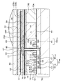
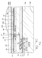
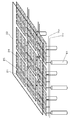
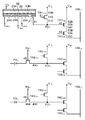
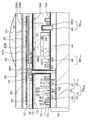
도 78에 종래의 적층형 촬상 소자(적층형 고체 촬상 장치)의 구성례를 도시한다. 도 78에 도시하는 예에서는, 반도체 기판(370) 내에, 제2 타입의 촬상 소자인 제3 촬상 소자(343) 및 제2 촬상 소자(341)를 구성하는 제2 타입의 광전변환부인 제3광전변환부(343A) 및 제2광전변환부(341A)가 적층되어, 형성되어 있다. 또한, 반도체 기판(370)의 상방(구체적으로는, 제2 촬상 소자(341)의 상방)에는, 제1 타입의 광전변환부인 제1광전변환부(310A)가 배치되어 있다. 여기서, 제1광전변환부(310A)는, 제1 전극(321), 유기 재료로 이루어지는 광전변환층(323), 제2 전극(322)을 구비하고 있고, 제1 타입의 촬상 소자인 제1 촬상 소자(310)를 구성한다. 제2광전변환부(341A) 및 제3광전변환부(343A)에서는, 흡수 계수의 차이에 의해, 각각, 예를 들면, 청색광 및 적색광이 광전변환된다. 또한, 제1광전변환부(310A)에서는, 예를 들면, 녹색광이 광전변환된다.Fig. 78 shows a configuration example of a conventional stacked imaging device (stacked solid-state imaging device). In the example shown in Fig. 78, in the
제2광전변환부(341A) 및 제3광전변환부(343A)에서 광전변환에 의해 생성한 전하는, 이들의 제2광전변환부(341A) 및 제3광전변환부(343A)에 일단 축적된 후, 각각, 종형 트랜지스터(게이트부(345)를 나타낸다)와 전송 트랜지스터(게이트부(346)를 나타낸다)에 의해 제2 부유 확산층(Floating Diffusion)(FD2) 및 제3 부유 확산층(FD3)에 전송되고, 또한, 외부의 판독 회로(도시 생략)에 출력된다. 이들의 트랜지스터 및 부유 확산층(FD2, FD3)도 반도체 기판(370)에 형성되어 있다.After the charges generated by photoelectric conversion in the second
제1광전변환부(310A)에서 광전변환에 의해 생성한 전하는, 콘택트 홀부(361), 배선층(362)을 통하여, 반도체 기판(370)에 형성된 제1 부유 확산층(FD1)에 축적된다. 또한, 제1광전변환부(310A)는, 콘택트 홀부(361), 배선층(362)을 통하여, 전하량을 전압으로 변환하는 증폭 트랜지스터의 게이트부(352)에도 접속되어 있다. 그리고, 제1 부유 확산층(FD1)은, 리셋·트랜지스터(게이트부(351)를 나타낸다)의 일부를 구성하고 있다. 참조 번호 371은 소자 분리 영역이고, 참조 번호 372는 반도체 기판(370)의 표면에 형성된 산화막이고, 참조 번호 376, 381은 층간 절연층이고, 참조 번호 383은 절연층이고, 참조 번호 314는 온 칩·마이크로·렌즈이다.The charge generated by the photoelectric conversion in the first
그런데, 상기한 일본 특개2016-63165호 공보에 개시된 기술에서는, 반도체층을 구성하는 재료로서, 예를 들면, IGZO가 들어져 있다. 그렇지만, IGZO로 이루어지는 반도체층을 이용하는 경우, 광전변환층을 구성하는 유기 반도체 재료의 상태밀도(狀態密度)와 반도체층을 구성하는 IGZO의 상태밀도의 차(差)가 크다. 예를 들면, 유기 반도체 재료의 상태밀도로서 1×10²¹㎝-3 정도, IGZO의 상태밀도로서 1×10¹⁸㎝-3 정도를 예시할 수 있다. 그 때문에, 광전변환에 의해 발생한 캐리어(예를 들면, 광전자)가 광전변환층으로부터 반도체층에 유입할 때, 광전변환층과 반도체층의 계면에서 캐리어의 정체(停滯)가 생기기 쉽고, 그 결과, 촬상 소자(광전변환 소자)의 광응답성에 악영향을 미친다는 문제가 있다.By the way, in the technique disclosed in the above-mentioned Japanese Patent Application Laid-open No. 2016-63165, as a material constituting the semiconductor layer, for example, IGZO is contained. However, when using a semiconductor layer made of IGZO, the difference between the state density of the organic semiconductor material constituting the photoelectric conversion layer and the state density of IGZO constituting the semiconductor layer is large. For example, about 1 × 10 21 cm -3 as the state density of the organic semiconductor material, and about 1 × 10 18 cm -3 as the state density of the IGZO can be exemplified. Therefore, when carriers (for example, photoelectrons) generated by photoelectric conversion flow from the photoelectric conversion layer to the semiconductor layer, carriers are likely to occur at the interface between the photoelectric conversion layer and the semiconductor layer, and as a result, There is a problem that it adversely affects the photoresponsiveness of the imaging element (photoelectric conversion element).
따라서 본 개시의 목적은, 광응답성에 악영향이 생기기 어려운 구성, 구조를 갖는 촬상 소자, 즉, 광전변환층에 축적된 전하의 전송 특성에 우수한 촬상 소자, 및, 관한 촬상 소자를 구비한 적층형 촬상 소자 및 고체 촬상 장치를 제공하는 것에 있다.Accordingly, an object of the present disclosure is to form an imaging element having a structure and structure that is unlikely to adversely affect photoresponsability, that is, an imaging element excellent in the transfer characteristics of charges accumulated in the photoelectric conversion layer, and a stacked-type imaging element comprising an imaging element relating to it. And a solid-state imaging device.
상기한 목적을 달성하기 위한 본 개시의 제1의 양태에 관한 촬상 소자(광전변환 소자)는,An imaging element (photoelectric conversion element) according to the first aspect of the present disclosure for achieving the above object,
제1 전극, 광전변환층 및 제2 전극이 적층되어 이루어지는 광전변환부를 구비하고 있고,The first electrode, the photoelectric conversion layer and the second electrode is provided with a photoelectric conversion unit made of a stack,
제1 전극과 광전변환층의 사이에는, 인듐복합산화물로 이루어지는 복합산화물층이 형성되어 있고,A composite oxide layer made of indium composite oxide is formed between the first electrode and the photoelectric conversion layer,
복합산화물층은, 제1 전극에 인접한 제1층, 및, 광전변환층에 인접한 제2층을 구비하고 있고,The composite oxide layer includes a first layer adjacent to the first electrode, and a second layer adjacent to the photoelectric conversion layer,
제1층에서의 인듐 조성은, 제2층에서의 인듐 조성보다도 높다.The indium composition in the first layer is higher than the indium composition in the second layer.
상기한 목적을 달성하기 위한 본 개시의 제2의 양태에 관한 촬상 소자(광전변환 소자)는,An imaging element (photoelectric conversion element) according to a second aspect of the present disclosure for achieving the above object,
제1 전극, 광전변환층 및 제2 전극이 적층되어 이루어지는 광전변환부를 구비하고 있고,The first electrode, the photoelectric conversion layer and the second electrode is provided with a photoelectric conversion unit made of a stack,
제1 전극과 광전변환층의 사이에는, 인듐-갈륨-아연복합산화물로 이루어지는 복합산화물층이 형성되어 있고,A composite oxide layer made of indium-gallium-zinc composite oxide is formed between the first electrode and the photoelectric conversion layer,
복합산화물층은, 제1 전극에 인접한 제1층, 및, 광전변환층에 인접한 제2층을 구비하고 있고,The composite oxide layer includes a first layer adjacent to the first electrode, and a second layer adjacent to the photoelectric conversion layer,
제1층에서의 인듐 조성은, 제2층에서의 인듐 조성보다도 높고, 또는,The indium composition in the first layer is higher than the indium composition in the second layer, or
제1층에서의 갈륨 조성은, 제2층에서의 갈륨 조성보다도 낮고, 또는,The gallium composition in the first layer is lower than the gallium composition in the second layer, or
제1층에서의 아연 조성은, 제2층에서의 아연 조성보다도 높다. 또는 또한, 제1층에서의 산소 원자 함유율은, 제2층에서의 산소 원자 함유율보다도 낮다.The zinc composition in the first layer is higher than the zinc composition in the second layer. Alternatively, the oxygen atom content in the first layer is lower than the oxygen atom content in the second layer.
상기한 목적을 달성하기 위한 본 개시의 제3의 양태에 관한 촬상 소자(광전변환 소자)는,An imaging element (photoelectric conversion element) according to a third aspect of the present disclosure for achieving the above object,
제1 전극, 광전변환층 및 제2 전극이 적층되어 이루어지는 광전변환부를 구비하고 있고,The first electrode, the photoelectric conversion layer and the second electrode is provided with a photoelectric conversion unit made of a stack,
제1 전극과 광전변환층의 사이에는, 인듐복합산화물(또는, 인듐-갈륨-아연복합산화물)로 이루어지는 복합산화물층이 형성되어 있고,Between the first electrode and the photoelectric conversion layer, a composite oxide layer made of indium composite oxide (or indium-gallium-zinc composite oxide) is formed,
복합산화물층은, 제1 전극에 인접한 제1층, 및, 광전변환층에 인접한 제2층을 구비하고 있고,The composite oxide layer includes a first layer adjacent to the first electrode, and a second layer adjacent to the photoelectric conversion layer,
제1층은, 제2층보다도 높은 캐리어 이동도를 갖는다.The first layer has a higher carrier mobility than the second layer.
상기한 목적을 달성하기 위한 본 개시의 제4의 양태에 관한 촬상 소자(광전변환 소자)는,An imaging element (photoelectric conversion element) according to a fourth aspect of the present disclosure for achieving the above object,
제1 전극, 광전변환층 및 제2 전극이 적층되어 이루어지는 광전변환부를 구비하고 있고,The first electrode, the photoelectric conversion layer and the second electrode is provided with a photoelectric conversion unit made of a stack,
제1 전극과 광전변환층의 사이에는, 인듐복합산화물(또는, 인듐-갈륨-아연복합산화물)로 이루어지는 복합산화물층이 형성되어 있고,Between the first electrode and the photoelectric conversion layer, a composite oxide layer made of indium composite oxide (or indium-gallium-zinc composite oxide) is formed,
복합산화물층은, 제1 전극에 인접한 제1층, 및, 광전변환층에 인접한 제2층을 구비하고 있고,The composite oxide layer includes a first layer adjacent to the first electrode, and a second layer adjacent to the photoelectric conversion layer,
제1층은, 제2층보다도 낮은 상태밀도(狀態密度)를 갖는다.The first layer has a lower state density than the second layer.
상기한 목적을 달성하기 위한 본 개시의 적층형 촬상 소자는, 본 개시의 제1의 양태∼제4의 양태에 관한 촬상 소자를 적어도 하나 갖는다.The stacked-type imaging element of the present disclosure for achieving the above object has at least one imaging element according to the first to fourth aspects of the present disclosure.
상기한 목적을 달성하기 위한 본 개시의 제1의 양태에 관한 고체 촬상 장치는, 본 개시의 제1의 양태∼제4의 양태에 관한 촬상 소자를, 복수, 구비하고 있다. 또한, 상기한 목적을 달성하기 위한 본 개시의 제2의 양태에 관한 고체 촬상 장치는, 본 개시의 적층형 촬상 소자를, 복수, 구비하고 있다.The solid-state imaging device according to the first aspect of the present disclosure for achieving the above object is provided with a plurality of imaging elements according to the first to fourth aspects of the present disclosure. In addition, the solid-state imaging device according to the second aspect of the present disclosure for achieving the above object is provided with a plurality of stacked imaging devices of the present disclosure.
본 개시의 제1의 양태∼제2의 양태에 관한 촬상 소자 등(후술한다)에서는, 적어도 2층을 갖는 복합산화물층에서 각 층의 조성이 규정되어 있고, 본 개시의 제3의 양태∼제4의 양태에 관한 촬상 소자 등(후술한다)에서는, 적어도 2층을 갖는 복합산화물층에서 각 층의 캐리어 이동도 또는 상태밀도의 관계가 규정되어 있다. 따라서, 광전변환에 의해 발생한 캐리어(예를 들면, 광전자)가 광전변환층으로부터 복합산화물층에 유입할 때, 광전변환층과 복합산화물층의 계면에서 캐리어의 정체가 생기기 어렵고, 또한, 광전변환층 및 복합산화물층, 전체로서의 캐리어의 수송 능력을 높일 수 있기 때문에, 촬상 소자의 광응답성에 악영향을 미치는 일이 없고, 광전변환층에 축적된 전하의 전송 특성에 우수한 촬상 소자를 제공할 수 있다. 게다가, 본 개시의 촬상 소자 등(후술한다)에서는, 복합산화물층과 광전변환층의 2층 구조로 되어 있기 때문에, 전하 축적시의 재결합을 방지할 수 있고, 광전변환층에 축적한 전하의 제1 전극에의 전송 효율을 증가시킬 수 있고, 암전류의 생성을 억제할 수 있다. 또한, 본 명세서에 기재된 효과는 어디까지나 예시이고 한정되는 것이 아니며, 또한, 부가적인 효과가 있어도 좋다.In the imaging elements and the like (to be described later) according to the first to second aspects of the present disclosure, the composition of each layer is defined in the composite oxide layer having at least two layers, and the third to the third embodiments of the present disclosure In the imaging element or the like (described later) according to the
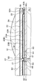
도 1은, 실시례 1의 촬상 소자의 모식적인 일부 단면도.
도 2는, 실시례 1의 촬상 소자의 등가 회로도.
도 3은, 실시례 1의 촬상 소자의 등가 회로도.
도 4는, 실시례 1의 촬상 소자를 구성하는 제1 전극 및 전하 축적용 전극 및 제어부를 구성하는 트랜지스터의 모식적인 배치도.
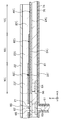
도 5는, 실시례 1의 촬상 소자의 동작시의 각 부위에서의 전위의 상태를 모식적으로 도시하는 도면.
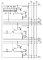
도 6A, 도 6B 및 도 6C는, 도 5(실시례 1), 도 20 및 도 21(실시례 4) 및 도 32 및 도 33(실시례 6)의 각 부위를 설명하기 위한 실시례 1, 실시례 4 및 실시례 6의 촬상 소자의 등가 회로도.
도 7은, 실시례 1의 촬상 소자를 구성하는 제1 전극 및 전하 축적용 전극의 모식적인 배치도.
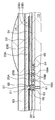
도 8은, 실시례 1의 촬상 소자를 구성하는 제1 전극, 전하 축적용 전극, 제2 전극 및 콘택트 홀부의 모식적인 투시 사시도.
도 9는, 실시례 1의 촬상 소자의 변형례의 등가 회로도.
도 10은, 도 9에 도시한 실시례 1의 촬상 소자의 변형례를 구성하는 제1 전극 및 전하 축적용 전극 및 제어부를 구성하는 트랜지스터의 모식적인 배치도.
도 11은, 실시례 2의 촬상 소자의 모식적인 일부 단면도.
도 12는, 실시례 3의 촬상 소자의 모식적인 일부 단면도.
도 13은, 실시례 3의 촬상 소자의 변형례의 모식적인 일부 단면도.
도 14는, 실시례 3의 촬상 소자의 다른 변형례의 모식적인 일부 단면도.
도 15는, 실시례 3의 촬상 소자의 또 다른 변형례의 모식적인 일부 단면도.
도 16은, 실시례 4의 촬상 소자의 일부분의 모식적인 일부 단면도.
도 17은, 실시례 4의 촬상 소자의 등가 회로도.
도 18은, 실시례 4의 촬상 소자의 등가 회로도.
도 19는, 실시례 4의 촬상 소자를 구성하는 제1 전극, 전송 제어용 전극 및 전하 축적용 전극 및 제어부를 구성하는 트랜지스터의 모식적인 배치도.
도 20은, 실시례 4의 촬상 소자의 동작시의 각 부위에서의 전위의 상태를 모식적으로 도시하는 도면.
도 21은, 실시례 4의 촬상 소자의 다른 동작시의 각 부위에서의 전위의 상태를 모식적으로 도시하는 도면.
도 22는, 실시례 4의 촬상 소자를 구성하는 제1 전극, 전송 제어용 전극 및 전하 축적용 전극의 모식적인 배치도.
도 23은, 실시례 4의 촬상 소자를 구성하는 제1 전극, 전송 제어용 전극, 전하 축적용 전극, 제2 전극 및 콘택트 홀부의 모식적인 투시 사시도.
도 24는, 실시례 4의 촬상 소자의 변형례를 구성하는 제1 전극, 전송 제어용 전극 및 전하 축적용 전극 및 제어부를 구성하는 트랜지스터의 모식적인 배치도.
도 25는, 실시례 5의 촬상 소자의 일부분의 모식적인 일부 단면도.
도 26은, 실시례 5의 촬상 소자를 구성하는 제1 전극, 전하 축적용 전극 및 전하 배출 전극의 모식적인 배치도.
도 27은, 실시례 5의 촬상 소자를 구성하는 제1 전극, 전하 축적용 전극, 전하 배출 전극, 제2 전극 및 콘택트 홀부의 모식적인 투시 사시도.
도 28은, 실시례 6의 촬상 소자의 모식적인 일부 단면도.
도 29는, 실시례 6의 촬상 소자의 등가 회로도.
도 30은, 실시례 6의 촬상 소자의 등가 회로도.
도 31은, 실시례 6의 촬상 소자를 구성하는 제1 전극 및 전하 축적용 전극 및 제어부를 구성하는 트랜지스터의 모식적인 배치도.
도 32는, 실시례 6의 촬상 소자의 동작시의 각 부위에서의 전위의 상태를 모식적으로 도시하는 도면.
도 33은, 실시례 6의 촬상 소자의 다른 동작시(전송시)의 각 부위에서의 전위의 상태를 모식적으로 도시하는 도면.
도 34는, 실시례 6의 촬상 소자를 구성하는 제1 전극 및 전하 축적용 전극의 모식적인 배치도.
도 35는, 실시례 6의 촬상 소자를 구성하는 제1 전극, 전하 축적용 전극, 제2 전극 및 콘택트 홀부의 모식적인 투시 사시도.
도 36은, 실시례 6의 촬상 소자의 변형례를 구성하는 제1 전극 및 전하 축적용 전극의 모식적인 배치도.
도 37은, 실시례 7의 촬상 소자의 모식적인 일부 단면도.
도 38은, 실시례 7의 촬상 소자에서의 전하 축적용 전극, 광전변환층 및 제2 전극이 적층된 부분을 확대한 모식적인 일부 단면도.
도 39는, 실시례 7의 촬상 소자의 변형례를 구성하는 제1 전극 및 전하 축적용 전극 및 제어부를 구성하는 트랜지스터의 모식적인 배치도.
도 40은, 실시례 8의 촬상 소자에서의 전하 축적용 전극, 광전변환층 및 제2 전극이 적층된 부분을 확대한 모식적인 일부 단면도.
도 41은, 실시례 9의 촬상 소자의 모식적인 일부 단면도.
도 42는, 실시례 10 및 실시례 11의 촬상 소자의 모식적인 일부 단면도.
도 43A 및 도 43B는, 실시례 11에서의 전하 축적용 전극 세그먼트의 모식적인 평면도.
도 44A 및 도 44B는, 실시례 11에서의 전하 축적용 전극 세그먼트의 모식적인 평면도.
도 45는, 실시례 11의 촬상 소자를 구성하는 제1 전극 및 전하 축적용 전극 및 제어부를 구성하는 트랜지스터의 모식적인 배치도.
도 46은, 실시례 11의 촬상 소자의 변형례를 구성하는 제1 전극 및 전하 축적용 전극의 모식적인 배치도.
도 47은, 실시례 12 및 실시례 11의 촬상 소자의 모식적인 일부 단면도.
도 48A 및 도 48B는, 실시례 12에서의 전하 축적용 전극 세그먼트의 모식적인 평면도.
도 49는, 실시례 13의 고체 촬상 장치에서의 제1 전극 및 전하 축적용 전극 세그먼트의 모식적인 평면도.
도 50은, 실시례 13의 고체 촬상 장치의 제1 변형례에서의 제1 전극 및 전하 축적용 전극 세그먼트의 모식적인 평면도.
도 51은, 실시례 13의 고체 촬상 장치의 제2 변형례에서의 제1 전극 및 전하 축적용 전극 세그먼트의 모식적인 평면도.
도 52는, 실시례 13의 고체 촬상 장치의 제3 변형례에서의 제1 전극 및 전하 축적용 전극 세그먼트의 모식적인 평면도.
도 53은, 실시례 13의 고체 촬상 장치의 제4 변형례에서의 제1 전극 및 전하 축적용 전극 세그먼트의 모식적인 평면도.
도 54는, 실시례 13의 고체 촬상 장치의 제5 변형례에서의 제1 전극 및 전하 축적용 전극 세그먼트의 모식적인 평면도.
도 55는, 실시례 13의 고체 촬상 장치의 제6 변형례에서의 제1 전극 및 전하 축적용 전극 세그먼트의 모식적인 평면도.
도 56은, 실시례 13의 고체 촬상 장치의 제7 변형례에서의 제1 전극 및 전하 축적용 전극 세그먼트의 모식적인 평면도.
도 57은, 실시례 13의 고체 촬상 장치의 제8 변형례에서의 제1 전극 및 전하 축적용 전극 세그먼트의 모식적인 평면도.
도 58은, 실시례 13의 고체 촬상 장치의 제9 변형례에서의 제1 전극 및 전하 축적용 전극 세그먼트의 모식적인 평면도.
도 59A, 도 59B 및 도 59C는, 실시례 13의 촬상 소자 블록에서의 판독 구동례를 도시하는 차트.
도 60은, 실시례 14의 고체 촬상 장치에서의 제1 전극 및 전하 축적용 전극 세그먼트의 모식적인 평면도.
도 61은, 실시례 14의 고체 촬상 장치의 변형례에서의 제1 전극 및 전하 축적용 전극 세그먼트의 모식적인 평면도.
도 62는, 실시례 14의 고체 촬상 장치의 변형례에서의 제1 전극 및 전하 축적용 전극 세그먼트의 모식적인 평면도.
도 63은, 실시례 14의 고체 촬상 장치의 변형례에서의 제1 전극 및 전하 축적용 전극 세그먼트의 모식적인 평면도.
도 64는, 실시례 1의 촬상 소자의 다른 변형례의 모식적인 일부 단면도.
도 65는, 실시례 1의 촬상 소자의 또 다른 변형례의 모식적인 일부 단면도.
도 66A, 도 66B 및 도 66C는, 실시례 1의 촬상 소자의 또 다른 변형례의 제1 전극의 부분 등이 확대된 모식적인 일부 단면도.
도 67은, 실시례 5의 촬상 소자의 다른 변형례의 전하 배출 전극의 부분 등이 확대된 모식적인 일부 단면도.
도 68은, 실시례 1의 촬상 소자의 또 다른 변형례의 모식적인 일부 단면도.
도 69는, 실시례 1의 촬상 소자의 또 다른 변형례의 모식적인 일부 단면도.
도 70은, 실시례 1의 촬상 소자의 또 다른 변형례의 모식적인 일부 단면도.
도 71은, 실시례 4의 촬상 소자의 다른 변형례의 모식적인 일부 단면도.
도 72는, 실시례 1의 촬상 소자의 또 다른 변형례의 모식적인 일부 단면도.
도 73은, 실시례 4의 촬상 소자의 또 다른 변형례의 모식적인 일부 단면도.
도 74는, 실시례 7의 촬상 소자의 변형례에서의 전하 축적용 전극, 광전변환층 및 제2 전극이 적층된 부분을 확대한 모식적인 일부 단면도.
도 75는, 실시례 8의 촬상 소자의 변형례에서의 전하 축적용 전극, 광전변환층 및 제2 전극이 적층된 부분을 확대한 모식적인 일부 단면도.
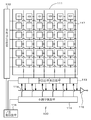
도 76은, 실시례 1의 고체 촬상 장치의 개념도.
도 77은, 본 개시의 촬상 소자 등으로 구성된 고체 촬상 장치를 전자 기기(카메라)를 이용한 예의 개념도.
도 78은, 종래의 적층형 촬상 소자(적층형 고체 촬상 장치)의 개념도.1 is a schematic partial cross-sectional view of the imaging device of Example 1. FIG.
2 is an equivalent circuit diagram of the imaging device of Example 1. FIG.
3 is an equivalent circuit diagram of the imaging device of Example 1. FIG.
4 is a schematic layout view of a transistor constituting a first electrode constituting the imaging element of Example 1, an electrode for charge accumulation, and a control unit.
Fig. 5 is a diagram schematically showing the state of potential at each site during operation of the imaging device of Example 1;
6A, 6B, and 6C are Example 1 for explaining each part of FIGS. 5 (Example 1), 20 and 21 (Example 4), and FIGS. 32 and 33 (Example 6); Equivalent circuit diagram of the imaging element of Example 4 and Example 6.
7 is a schematic arrangement diagram of a first electrode and an electrode for charge accumulation constituting the imaging element of Example 1. FIG.
8 is a schematic perspective perspective view of a first electrode, a charge storage electrode, a second electrode, and a contact hole portion constituting the imaging device of Example 1. FIG.
9 is an equivalent circuit diagram of a modification of the imaging element of Example 1. FIG.
10 is a schematic layout view of a transistor constituting a first electrode, a charge storage electrode, and a control unit constituting a modification of the imaging device of Example 1 shown in FIG. 9.
11 is a schematic partial cross-sectional view of the imaging device of Example 2;
12 is a schematic partial cross-sectional view of the imaging device of Example 3;
13 is a schematic partial cross-sectional view of a modification of the imaging element of Example 3;
14 is a schematic partial cross-sectional view of another modification of the imaging device of Example 3;
15 is a schematic partial cross-sectional view of still another modification of the imaging element of Example 3;
16 is a schematic partial cross-sectional view of a part of the imaging device of Example 4;
17 is an equivalent circuit diagram of the imaging device of Example 4. FIG.
18 is an equivalent circuit diagram of the imaging device of Example 4. FIG.
19 is a schematic layout diagram of a first electrode constituting the imaging element of Example 4, an electrode for transfer control, an electrode for charge accumulation, and a transistor constituting a control unit.
Fig. 20 is a diagram schematically showing the state of potential at each site during operation of the imaging element of Example 4;
Fig. 21 is a diagram schematically showing the state of potential at each site during different operations of the imaging device of Example 4;
22 is a schematic layout diagram of a first electrode, a transfer control electrode, and a charge storage electrode constituting the imaging device of Example 4. FIG.
23 is a schematic perspective perspective view of a first electrode, a transfer control electrode, a charge accumulation electrode, a second electrode, and a contact hole portion constituting the imaging element of Example 4. FIG.
24 is a schematic layout diagram of a transistor constituting a first electrode, a transfer control electrode, a charge storage electrode, and a control unit constituting a modification of the imaging device of Example 4;
25 is a schematic partial cross-sectional view of a part of the imaging device of Example 5. FIG.
26 is a schematic layout view of a first electrode, a charge accumulation electrode, and a charge discharge electrode constituting the imaging element of Example 5. FIG.
Fig. 27 is a schematic perspective perspective view of a first electrode, a charge accumulation electrode, a charge discharge electrode, a second electrode, and a contact hole part constituting the imaging device of Example 5.
28 is a schematic partial cross-sectional view of the imaging device of Example 6. FIG.
29 is an equivalent circuit diagram of the imaging device of Example 6. FIG.
30 is an equivalent circuit diagram of the imaging device of Example 6. FIG.
31 is a schematic layout view of a transistor constituting a first electrode constituting the imaging element of Example 6, an electrode for charge accumulation, and a control unit.
Fig. 32 is a diagram schematically showing the state of potential at each site during operation of the imaging device of Example 6.
Fig. 33 is a diagram schematically showing the state of dislocations at each site during another operation (transmission) of the imaging device of Example 6;
34 is a schematic layout view of the first electrode and the charge storage electrode constituting the imaging element of Example 6. FIG.
35 is a schematic perspective perspective view of a first electrode, a charge storage electrode, a second electrode, and a contact hole portion constituting the imaging element of Example 6. FIG.
36 is a schematic layout diagram of a first electrode and a charge storage electrode constituting a modification of the imaging element of Example 6. FIG.
37 is a schematic partial cross-sectional view of the imaging device of Example 7. FIG.
FIG. 38 is a schematic partial cross-sectional view of an enlarged portion of a charge accumulation electrode, a photoelectric conversion layer, and a second electrode stacked in the imaging device of Example 7. FIG.
39 is a schematic layout view of a transistor constituting a first electrode, a charge accumulation electrode, and a control unit constituting a modification of the imaging element of Example 7. FIG.
Fig. 40 is a schematic partial cross-sectional view of an enlarged portion of a charge accumulation electrode, a photoelectric conversion layer, and a second electrode stacked in the imaging device of Example 8;
41 is a schematic partial cross-sectional view of the imaging device of Example 9;
42 is a schematic partial cross-sectional view of the imaging device of Examples 10 and 11;
43A and 43B are schematic plan views of an electrode segment for charge accumulation in Example 11;
44A and 44B are schematic plan views of an electrode segment for charge accumulation in Example 11;
Fig. 45 is a schematic layout diagram of the first electrode constituting the imaging element of Example 11, the electrode for charge accumulation, and the transistor constituting the control unit.
46 is a schematic layout view of a first electrode and a charge storage electrode constituting a modification of the imaging element of Example 11;
47 is a schematic partial cross-sectional view of the imaging device of Examples 12 and 11.
48A and 48B are schematic plan views of the electrode segments for charge accumulation in Example 12;
49 is a schematic plan view of a first electrode and an electrode segment for charge accumulation in the solid-state imaging device of Example 13. FIG.
50 is a schematic plan view of the first electrode and the electrode segment for charge accumulation in the first modification of the solid-state imaging device of Example 13. FIG.
51 is a schematic plan view of the first electrode and the electrode segment for charge accumulation in the second modification of the solid-state imaging device of Example 13. FIG.
52 is a schematic plan view of a first electrode and an electrode segment for charge accumulation in a third modification of the solid-state imaging device of Example 13;
53 is a schematic plan view of the first electrode and the electrode segment for charge accumulation in the fourth modification of the solid-state imaging device of Example 13. FIG.
54 is a schematic plan view of a first electrode and an electrode segment for charge accumulation in a fifth modification of the solid-state imaging device of Example 13. FIG.
55 is a schematic plan view of the first electrode and the electrode segment for charge accumulation in the sixth modification of the solid-state imaging device of Example 13. FIG.
56 is a schematic plan view of the first electrode and the electrode segment for charge accumulation in the seventh modification of the solid-state imaging device of Example 13. FIG.
57 is a schematic plan view of the first electrode and the electrode segment for charge accumulation in the eighth modification of the solid-state imaging device of Example 13. FIG.
58 is a schematic plan view of the first electrode and the electrode segment for charge accumulation in the ninth modification of the solid-state imaging device of Example 13. FIG.
59A, 59B, and 59C are charts showing a read driving example in the imaging element block of Example 13. FIG.
60 is a schematic plan view of a first electrode and an electrode segment for charge accumulation in the solid-state imaging device of Example 14;
61 is a schematic plan view of a first electrode and an electrode segment for charge accumulation in a modification of the solid-state imaging device of Example 14;
62 is a schematic plan view of a first electrode and an electrode segment for charge accumulation in a modification of the solid-state imaging device of Example 14;
63 is a schematic plan view of a first electrode and an electrode segment for charge accumulation in a modification of the solid-state imaging device of Example 14;
64 is a schematic partial cross-sectional view of another modification of the imaging element of Example 1;
65 is a schematic partial cross-sectional view of still another modification of the imaging element of Example 1. FIG.
66A, 66B, and 66C are schematic partial cross-sectional views, in which a portion of the first electrode and the like of another modification of the imaging element of Example 1 are enlarged.
67 is a schematic partial cross-sectional view of an enlarged portion of a charge discharge electrode of another modified example of the imaging device of Example 5;
68 is a schematic partial cross-sectional view of still another modification of the imaging element of Example 1;
69 is a schematic partial cross-sectional view of still another modification of the imaging element of Example 1;
70 is a schematic partial cross-sectional view of still another modification of the imaging element of Example 1. FIG.
71 is a schematic partial cross-sectional view of another modification of the imaging device of Example 4;
72 is a schematic partial cross-sectional view of still another modification of the imaging element of Example 1;
73 is a schematic partial cross-sectional view of still another modification of the imaging element of Example 4;
74 is a schematic partial cross-sectional view of an enlarged portion of a charge accumulation electrode, a photoelectric conversion layer, and a second electrode in a modification of the imaging device of Example 7;
Fig. 75 is a schematic partial cross-sectional view of an enlarged portion of a charge accumulation electrode, a photoelectric conversion layer, and a second electrode in a modification of the imaging device of Example 8;
76 is a conceptual diagram of the solid-state imaging device of Example 1. FIG.
77 is a conceptual diagram of an example using an electronic device (camera) for a solid-state imaging device composed of the imaging device of the present disclosure.
Fig. 78 is a conceptual diagram of a conventional stacked imaging device (stacked solid-state imaging device).
이하, 도면을 참조하여, 실시례에 의거하여 본 개시를 설명하는데, 본 개시는 실시례로 한정되는 것이 아니고, 실시례에서의 여러 가지의 수치나 재료는 예시이다. 또한, 설명은, 이하의 순서로 행한다.Hereinafter, the present disclosure will be described based on examples with reference to the drawings, but the present disclosure is not limited to the examples, and various numerical values and materials in the examples are examples. In addition, description is performed in the following procedure.
1. 본 개시의 제1의 양태∼제4의 양태에 관한 촬상 소자, 본 개시의 적층형 촬상 소자, 본 개시의 제1의 양태∼제2의 양태에 관한 고체 촬상 장치, 전반에 관한 설명1. Imaging element according to first to fourth aspects of the present disclosure, stacked image pickup element of the present disclosure, solid-state imaging device according to first to second aspects of the present disclosure, and overall description
2. 실시례 1(본 개시의 제1의 양태∼제4의 양태에 관한 촬상 소자, 본 개시의 적층형 촬상 소자, 본 개시의 제2의 양태에 관한 고체 촬상 장치)2. Example 1 (image pickup device according to first to fourth aspects of the present disclosure, stacked image pickup device of the present disclosure, solid-state imaging device according to the second aspect of the present disclosure)
3.실시례 2(실시례 1의 변형)3. Example 2 (Variation of Example 1)
4. 실시례 3(실시례 1∼실시례 2의 변형, 본 개시의 제1의 양태에 관한 고체 촬상 장치)4. Example 3 (a modification of Examples 1 to 2, a solid-state imaging device according to the first aspect of the present disclosure)
5.실시례 4(실시례 1∼실시례 3의 변형, 전송 제어용 전극을 구비한 촬상 소자)5. Example 4 (Modifications of Examples 1 to 3, Imaging Device with Electrodes for Transmission Control)
6. 실시례 5(실시례 1∼실시례 4의 변형, 전하 배출 전극을 구비한 촬상 소자)6. Example 5 (Modifications of Examples 1 to 4, imaging device with charge discharge electrode)
7. 실시례 6(실시례 1∼실시례 5의 변형, 복수의 전하 축적용 전극 세그먼트를 구비한 촬상 소자)7. Example 6 (Modification of Examples 1 to 5, an imaging element having a plurality of electrode segments for charge accumulation)
8. 실시례 7(제1 구성 및 제6 구성의 촬상 소자)8. Example 7 (image pickup elements of first and sixth configurations)
9. 실시례 8(본 개시의 제2 구성 및 제6 구성의 촬상 소자)9. Example 8 (image pickup device of second and sixth configurations of the present disclosure)
10. 실시례 9(제3 구성의 촬상 소자)10. Example 9 (3rd configuration imaging device)
11. 실시례 10(제4 구성의 촬상 소자)11. Example 10 (4th configuration imaging device)
12. 실시례 11(제5 구성의 촬상 소자)12. Example 11 (5th configuration imaging device)
13.실시례 12(제6 구성의 촬상 소자)13.Example 12 (sixth configuration imaging element)
14. 실시례 13(제1 구성∼제2 구성의 고체 촬상 장치)14. Example 13 (solid-state imaging device of first to second configurations)
15.실시례 14(실시례 13의 변형)15. Example 14 (Variation of Example 13)
16. 기타16. Other
<본 개시의 제1의 양태∼제4의 양태에 관한 촬상 소자, 본 개시의 적층형 촬상 소자, 및 본 개시의 제1의 양태∼제2의 양태에 관한 고체 촬상 장치, 전반에 관한 설명><The imaging device according to the first aspect to the fourth aspect of the present disclosure, the stacked-type imaging device of the present disclosure, and the solid-state imaging device according to the first aspect to the second aspect of the present disclosure, and the overall description>
본 개시의 제1의 양태에 관한 촬상 소자, 본 개시의 적층형 촬상 소자를 구성하는 본 개시의 제1의 양태에 관한 촬상 소자, 및, 본 개시의 제1의 양태∼제2의 양태에 관한 고체 촬상 장치를 구성하는 본 개시의 제1의 양태에 관한 촬상 소자를, 총칭하여, 편의상, 『본 개시의 제1의 양태에 관한 촬상 소자 등』이라고 부르는 경우가 있다. 또한, 본 개시의 제2의 양태에 관한 촬상 소자, 본 개시의 적층형 촬상 소자를 구성하는 본 개시의 제2의 양태에 관한 촬상 소자, 및, 본 개시의 제1의 양태∼제2의 양태에 관한 고체 촬상 장치를 구성하는 본 개시의 제2의 양태에 관한 촬상 소자를, 총칭하여, 편의상, 『본 개시의 제2의 양태에 관한 촬상 소자 등』이라고 부르는 경우가 있다. 나아가서는, 본 개시의 제3의 양태에 관한 촬상 소자, 본 개시의 적층형 촬상 소자를 구성하는 본 개시의 제3의 양태에 관한 촬상 소자, 및, 본 개시의 제1의 양태∼제2의 양태에 관한 고체 촬상 장치를 구성하는 본 개시의 제3의 양태에 관한 촬상 소자를, 총칭하여, 편의상, 『본 개시의 제3의 양태에 관한 촬상 소자 등』이라고 부르는 경우가 있다. 또한, 본 개시의 제4의 양태에 관한 촬상 소자, 본 개시의 적층형 촬상 소자를 구성하는 본 개시의 제4의 양태에 관한 촬상 소자, 및, 본 개시의 제1의 양태∼제2의 양태에 관한 고체 촬상 장치를 구성하는 본 개시의 제4의 양태에 관한 촬상 소자를, 총칭하여, 편의상, 『본 개시의 제4의 양태에 관한 촬상 소자 등』이라고 부르는 경우가 있다. 나아가서는, 본 개시의 제1의 양태∼제4의 양태에 관한 촬상 소자 등을, 총칭하여, 편의상, 『본 개시의 촬상 소자 등』이라고 부르는 경우가 있다.An imaging element according to the first aspect of the present disclosure, an imaging element according to the first aspect of the present disclosure constituting the multilayered imaging element of the present disclosure, and a solid according to the first aspect to the second aspect of the present disclosure The imaging element according to the first aspect of the present disclosure constituting the imaging device may be collectively referred to as "the imaging device according to the first aspect of the present disclosure" for convenience. In addition, the imaging device according to the second aspect of the present disclosure, the imaging device according to the second aspect of the present disclosure constituting the stacked imaging device of the present disclosure, and the first aspect to the second aspect of the present disclosure. The imaging element according to the second aspect of the present disclosure constituting the solid-state imaging device according to the present invention may be collectively referred to as "an imaging device according to the second aspect of the present disclosure" for convenience. Furthermore, the imaging device according to the third aspect of the present disclosure, the imaging device according to the third aspect of the present disclosure constituting the stacked imaging device of the present disclosure, and the first to second aspects of the present disclosure. The imaging element according to the third aspect of the present disclosure constituting the solid-state imaging device according to the present invention may be collectively referred to as "an imaging device according to the third aspect of the present disclosure" for convenience. In addition, the imaging device according to the fourth aspect of the present disclosure, the imaging device according to the fourth aspect of the present disclosure constituting the stacked imaging device of the present disclosure, and the first to second aspects of the present disclosure. The imaging element according to the fourth aspect of the present disclosure constituting the solid-state imaging device according to the present invention may be collectively referred to as "the imaging device according to the fourth aspect of the present disclosure" for convenience. Further, the imaging elements and the like according to the first to fourth aspects of the present disclosure are collectively referred to as "image pickup devices of the present disclosure" for convenience.
본 개시의 제2의 양태에 관한 촬상 소자 등에서, 인듐-갈륨-아연복합산화물을 (ZnO)X(Ga2O3)1-X, (Ga2O3)Y(In2O3)1-Y 및 (In2O3)Z(ZnO)1-Z로 표시한 때,In an imaging device or the like according to the second aspect of the present disclosure, indium-gallium-zinc composite oxide is (ZnO) X (Ga 2 O 3 ) 1-X , (Ga 2 O 3 ) Y (In 2 O 3 ) 1- When expressed as Y and (In 2 O 3 ) Z (ZnO) 1-Z ,
제1층에서의 X의 값은 제2층에서의 X의 값보다도 높고, 또는,The value of X in the first layer is higher than the value of X in the second layer, or
제1층에서의 Y의 값은 제2층에서의 Y의 값보다도 낮고, 또는,The value of Y in the first layer is lower than the value of Y in the second layer, or
제1층에서의 Z의 값은 제2층에서의 Z의 값보다도 높은 형태로 할 수 있다. 또한,The value of Z in the first layer can be set higher than the value of Z in the second layer. Also,
(1) 제1층에서의 X의 값은 제2층에서의 X의 값보다도 높은 케이스(1) Case where the value of X in the first layer is higher than the value of X in the second layer
(2) 제1층에서의 Y의 값은 제2층에서의 Y의 값보다도 낮은 케이스(2) The case where the value of Y in the first layer is lower than the value of Y in the second layer
(3) 제1층에서의 Z의 값은 제2층에서의 Z의 값보다도 높은 케이스(3) The case where the value of Z in the first layer is higher than the value of Z in the second layer
(4) 제1층에서의 X의 값은 제2층에서의 X의 값보다도 높고, 또한, 제1층에서의 Y의 값은 제2층에서의 Y의 값보다도 낮은 케이스(4) The value of X in the first layer is higher than the value of X in the second layer, and the value of Y in the first layer is lower than the value of Y in the second layer.
(5) 제1층에서의 X의 값은 제2층에서의 X의 값보다도 높고, 또한, 제1층에서의 Z의 값은 제2층에서의 Z의 값보다도 높은 케이스(5) The value of X in the first layer is higher than the value of X in the second layer, and the value of Z in the first layer is higher than the value of Z in the second layer.
(6) 제1층에서의 Y의 값은 제2층에서의 Y의 값보다도 낮고, 또한, 제1층에서의 Z의 값은 제2층에서의 Z의 값보다도 높은 케이스(6) The value of Y in the first layer is lower than the value of Y in the second layer, and the value of Z in the first layer is higher than the value of Z in the second layer.
(7) 제1층에서의 X의 값은 제2층에서의 X의 값보다도 높고, 또한, 제1층에서의 Y의 값은 제2층에서의 Y의 값보다도 낮고, 또한, 제1층에서의 Z의 값은 제2층에서의 Z의 값보다도 높은 케이스(7) The value of X in the first layer is higher than the value of X in the second layer, and the value of Y in the first layer is lower than the value of Y in the second layer, and the first layer Case in which the value of Z is higher than the value of Z in the second layer
의 7가지의 케이스를 들 수 있다. 그리고, 이 경우, 0<X<0.875, 0<Y<0.875, 0.125<Z<0.875(단, X+Y+Z=1.000)이고, 제1층에 관해서는 Y<0.5, 제2층에 관해서는 X<0.5, Y>0.5를 만족하는 것이 바람직하다.There are 7 cases. And in this case, 0 <X <0.875, 0 <Y <0.875, 0.125 <Z <0.875 (however, X + Y + Z = 1.000), for the first layer, Y <0.5, for the second layer It is preferable to satisfy X <0.5, Y> 0.5.
본 개시의 제3의 양태에 관한 촬상 소자 등에서는, 1×10⁻⁶≤(제2층의 캐리어 이동도)/(제1층의 캐리어 이동도)≤0.1을 만족하는 것이 바람직하다. 또한, 제1층의 캐리어 이동도는, 한정하는 것은 아니지만, 10㎠/V·s 이상인 것이 바람직하다.In the imaging element or the like according to the third aspect of the present disclosure, it is preferable to satisfy 1 × 10 −6 ≤ (carrier mobility of the second layer) / (carrier mobility of the first layer) ≤ 0.1. The carrier mobility of the first layer is not limited, but is preferably 10
본 개시의 촬상 소자 등에서, 복합산화물층은 비정질인(예를 들면, 국소적으로 결정 구조를 갖지 않는 비정질인) 것이 바람직하다. 복합산화물층이 비정질인지의 여부는, X선 회절 분석에 의거하여 결정할 수 있다.In the imaging device or the like of the present disclosure, it is preferable that the composite oxide layer is amorphous (for example, amorphous having no crystalline structure locally). Whether or not the composite oxide layer is amorphous can be determined based on X-ray diffraction analysis.
상기한 바람직한 형태, 구성을 포함하는 본 개시의 제1의 양태, 제3의 양태 또는 제4의 양태에 관한 촬상 소자 등에서, 복합산화물층(무기산화물 반도체 재료층)은, 인듐-갈륨-아연복합산화물(IGZO)로 이루어지는 구성으로 할 수 있다. 또한, 상기한 바람직한 형태, 구성을 포함하는 본 개시의 촬상 소자 등에서, 넓게는, 복합산화물층은, 입사광에 대해 투명한 도전성을 갖는 무기산화물 반도체 재료로 이루어진다. 또는 또한, 상기한 바람직한 형태, 구성을 포함하는 본 개시의 제1의 양태, 제3의 양태 또는 제4의 양태에 관한 촬상 소자 등에서, 복합산화물층(무기산화물 반도체 재료층)은, 인듐, 텅스텐, 주석 및 아연으로 이루어지는 군에서 선택되는 적어도 2종류의 원소로 구성되어 있는 형태로 할 수 있다. 즉, 구체적으로는, 복합산화물층(무기산화물 반도체 재료층)은, 산화인듐에 텅스텐(W)을 첨가한 재료인 인듐-텅스텐산화물(IWO), 산화인듐에 텅스텐(W) 및 아연(Zn)을 첨가한 재료인 인듐-텅스텐-아연산화물(IWZO), 산화인듐에 주석(Sn) 및 아연(Zn)을 첨가한 재료인 인듐-주석-아연산화물(ITZO), 또는, 아연-주석산화물(ZTO)로 이루어지는 구성으로 할 수 있다. 보다 구체적으로는, 복합산화물층은, In-W산화물로 이루어지고, 또는, In-Sn산화물, In-Zn산화물, 또는, W-Sn산화물, 또는, W-Zn산화물, 또는, Sn-Zn산화물, 또는, In-W-Sn산화물, 또는, In-W-Zn산화물, 또는, In-Sn-Zn산화물, 또는, In-W-Sn-Zn산화물로 이루어진다. IWO에서는, 인듐산화물과 텅스텐산화물의 합계 질량을 100질량%로 하였을 때, 텅스텐산화물의 질량 비율은 10질량% 내지 30질량%인 것이 바람직하다. 나아가서는, IWZO에서는, 인듐산화물과 텅스텐산화물과 Zn산화물의 합계 질량을 100질량%로 하였을 때, 텅스텐산화물의 질량 비율은 2질량% 내지 15질량%, Zn산화물의 질량 비율은 1질량% 내지 3질량%인 것이 바람직하다. 또한, ITZO에서는, 인듐산화물과 Zn산화물과 Sn산화물의 합계 질량을 100질량%로 하였을 때, 텅스텐산화물의 질량 비율은 3질량% 내지 10질량%, 주석산화물의 질량 비율은 10질량% 내지 17질량%인 것이 바람직하다. 단, 이들의 값으로 한정하는 것은 아니다. 또한, 복합산화물층(무기산화물 반도체 재료층)이 인듐, 텅스텐, 주석 및 아연으로 이루어지는 군에서 선택되는 적어도 2종류의 원소로 구성되어 있는 형태로 하는 경우, 조성변조(組成變調)에 의거하여 복합산화물층을 구성하는 제1층 및 제2층을 형성하면 좋다.In the imaging device according to the first aspect, the third aspect, or the fourth aspect of the present disclosure including the above-described preferred aspect and configuration, the composite oxide layer (inorganic oxide semiconductor material layer) is an indium-gallium-zinc composite It can be made of an oxide (IGZO). In addition, in the imaging device of the present disclosure including the above-described preferred form and configuration, the composite oxide layer is broadly made of an inorganic oxide semiconductor material having conductivity that is transparent to incident light. Alternatively, in the imaging device according to the first aspect, the third aspect, or the fourth aspect of the present disclosure including the above-described preferred form and configuration, the composite oxide layer (inorganic oxide semiconductor material layer) is indium or tungsten. , It may be in a form consisting of at least two types of elements selected from the group consisting of tin and zinc. That is, specifically, the composite oxide layer (inorganic oxide semiconductor material layer) is indium-tungsten oxide (IWO), in which tungsten (W) is added to indium oxide, tungsten (W), and zinc (Zn) to indium oxide. Material added with indium-tungsten-zinc oxide (IWZO), indium oxide with tin (Sn) and zinc (Zn), indium-tin-zinc oxide (ITZO), or zinc-tin oxide (ZTO ). More specifically, the composite oxide layer is made of In-W oxide, or In-Sn oxide, In-Zn oxide, or W-Sn oxide, or W-Zn oxide, or Sn-Zn oxide , Or, In-W-Sn oxide, or In-W-Zn oxide, or In-Sn-Zn oxide, or In-W-Sn-Zn oxide. In IWO, when the total mass of indium oxide and tungsten oxide is 100 mass%, the mass ratio of tungsten oxide is preferably 10 mass% to 30 mass%. Furthermore, in IWZO, when the total mass of indium oxide, tungsten oxide, and Zn oxide is 100% by mass, the mass ratio of tungsten oxide is 2% by mass to 15% by mass, and the mass ratio of Zn oxide is 1% by mass to 3% It is preferably mass%. In addition, in ITZO, when the total mass of indium oxide, Zn oxide, and Sn oxide is 100 mass%, the mass ratio of tungsten oxide is 3 mass% to 10 mass%, and the mass ratio of tin oxide is 10 mass% to 17 mass %. However, it is not limited to these values. In addition, when the composite oxide layer (inorganic oxide semiconductor material layer) is composed of at least two kinds of elements selected from the group consisting of indium, tungsten, tin, and zinc, the composite is based on compositional modulation. It is good to form the first layer and the second layer constituting the oxide layer.
본 개시의 촬상 소자 등에서, 복합산화물층은, 제1 전극에 인접한 제1층, 및, 광전변환층에 인접한 제2층을 구비하고 있는데, 제1층과 제2층이 적층된 구조로 할 수 있고, 제1층과 제2층의 사이에 중간층이 형성된 구조로 할 수도 있다.In the imaging device of the present disclosure, the composite oxide layer includes a first layer adjacent to the first electrode, and a second layer adjacent to the photoelectric conversion layer. The first layer and the second layer can be stacked. Alternatively, a structure in which an intermediate layer is formed between the first layer and the second layer may be used.
중간층을 갖는 본 개시의 제2의 양태에 관한 촬상 소자 등에서,In the imaging element and the like according to the second aspect of the present disclosure having an intermediate layer,
제1층에서의 X의 값은 중간층에서의 X의 값보다도 높고, 중간층에서의 X의 값은 제2층에서의 X의 값보다도 높고, 또는,The value of X in the first layer is higher than the value of X in the middle layer, and the value of X in the middle layer is higher than the value of X in the second layer, or
제1층에서의 Y의 값은 중간층에서의 Y의 값보다도 낮고, 중간층에서의 Y의 값은 제2층에서의 Y의 값보다도 낮고, 또는,The value of Y in the first layer is lower than the value of Y in the middle layer, and the value of Y in the middle layer is lower than the value of Y in the second layer, or
제1층에서의 Z의 값은 중간층에서의 Z의 값보다도 높고, 중간층에서의 Z의 값은 제2층에서의 Z의 값보다도 높은 형태로 할 수 있다.The value of Z in the first layer may be higher than the value of Z in the middle layer, and the value of Z in the middle layer may be higher than the value of Z in the second layer.
또한, 제1층에서의 산소 원자 함유율은, 중간층에서의 산소 원자 함유율보다도 낮고, 중간층에서의 산소 원자 함유율은, 제2층에서의 산소 원자 함유율보다도 낮은 형태로 할 수 있다.In addition, the oxygen atom content in the first layer is lower than the oxygen atom content in the intermediate layer, and the oxygen atom content in the intermediate layer can be made lower than the oxygen atom content in the second layer.
중간층은, X, Y, Z 등의 값이 다른 층이 2층 이상, 적층되어 이루어지는 구성으로 할 수도 있고(즉, 계단형상으로 X, Y, Z 등의 값이 다른 층 구성으로 할 수 있고), X, Y, Z 등의 값이 서서히 달라지는(변화하는) 구성으로 할 수도 있다.The intermediate layer may have a configuration in which two or more layers having different values of X, Y, Z, etc. are stacked (that is, a layer configuration in which values of X, Y, Z, etc. are different in a step shape). , X, Y, Z, etc. may be configured to gradually change (change).
또는 또한, 중간층을 갖는 본 개시의 제1의 양태에 관한 촬상 소자 등에서, 제1층에서의 인듐 조성은, 중간층에서의 인듐 조성보다도 높고, 중간층에서의 인듐 조성은, 제2층에서의 인듐 조성보다도 높은 형태로 할 수 있다. 그리고, 중간층은, 인듐 조성이 다른 층이 2층 이상, 적층되어 이루어지는 구성으로 할 수도 있고(즉, 계단형상으로 인듐 조성이 다른 층 구성으로 할 수 있고), 인듐 조성이 서서히 달라지는(변화하는) 구성으로 할 수도 있다.Or further, in the image pickup device according to the first aspect of the present disclosure having an intermediate layer, the indium composition in the first layer is higher than the indium composition in the intermediate layer, and the indium composition in the intermediate layer is the indium composition in the second layer. It can be made into a higher form. In addition, the intermediate layer may have a structure in which two or more layers having different indium compositions are stacked (that is, a stepwise structure may have a different indium composition), and the indium composition gradually changes (changes). You can also make it into a structure.
복합산화물층에서의 인듐 조성(인듐 원자 함유율)의 분석, 갈륨 조성(갈륨 원자 함유율)의 분석, 아연 조성(아연 원자 함유율)의 분석, 산소 원자 함유율의 분석은, 라더포드 후방산란분석법(RBS : Rutherford Backscattering Spectrometry), 또는, 라더포드 후방산란분석법과 핵반응 분석법과의 조합에 의거하여 행할 수 있다.The analysis of the indium composition (indium atom content) in the composite oxide layer, the analysis of the gallium composition (gallium atom content), the analysis of the zinc composition (zinc atom content), and the analysis of the oxygen atom content rate, the Latherford backscattering method (RBS: Rutherford Backscattering Spectrometry), or a combination of a Rutherford backscattering method and a nuclear reaction method.
또는 또한, 중간층을 갖는 본 개시의 제3의 양태에 관한 촬상 소자 등에서, 제1층은, 중간층보다도 높은 캐리어 이동도를 가지며, 중간층은, 제2층보다도 높은 캐리어 이동도를 갖는 형태로 할 수 있다. 그리고, 중간층은, 캐리어 이동도가 다른 층이 2층 이상, 적층되어 이루어지는 구성으로 할 수도 있고(즉, 계단형상으로 캐리어 이동도가 다른 층 구성으로 할 수 있고), 캐리어 이동도가 서서히 달라지는(변화하는) 구성으로 할 수도 있다.Alternatively, in the imaging device according to the third aspect of the present disclosure having an intermediate layer, the first layer may have a carrier mobility higher than that of the intermediate layer, and the intermediate layer may have a carrier mobility higher than that of the second layer. have. In addition, the intermediate layer may have a structure in which two or more layers having different carrier mobility are stacked (that is, it may have a layer configuration with different carrier mobility in a stepwise shape), and the carrier mobility may gradually change ( It can also be configured as a variable).
캐리어 이동도의 값은, 홀 측정이나 Time-of-Flight법에 의거하여 결정할 수 있다.The value of carrier mobility can be determined based on a hole measurement or a time-of-flight method.
또는 또한, 중간층을 갖는 본 개시의 제4의 양태에 관한 촬상 소자 등에서, 제1층은, 중간층보다도 낮은 상태밀도를 가지며, 중간층은, 제2층보다도 낮은 상태밀도를 갖는 형태로 할 수 있다. 그리고, 중간층은, 상태밀도가 다른 층이 2층 이상, 적층되어 이루어지는 구성으로 할 수도 있고(즉, 계단형상으로 상태밀도가 다른 층 구성으로 할 수 있고), 상태밀도가 서서히 달라지는(변화하는) 구성으로 할 수도 있다.Alternatively, in the imaging element or the like according to the fourth aspect of the present disclosure having an intermediate layer, the first layer may have a state density lower than that of the intermediate layer, and the intermediate layer may have a state density lower than that of the second layer. In addition, the intermediate layer may have a structure in which two or more layers having different state densities are stacked (i.e., can be made into a layer structure having a different state density in a staircase shape), and the state density gradually changes (varies). You can also make it into a structure.
중간층에서의 상태밀도의 값은, 역광전자 분광법에 의거하여 결정할 수 있다.The value of the state density in the intermediate layer can be determined based on reverse photoelectron spectroscopy.
복합산화물층은, 단층 구성(1종류의 재료로 구성)이라도 좋고, 다층 구성(2종류 이상의 재료로 구성)이라도 좋다. 또는 또한, 후술하는 전하 축적용 전극의 상방에 위치하는 복합산화물층을 구성하는 재료와, 제1 전극의 상방에 위치하는 복합산화물층을 구성하는 재료를, 다르게 할 수 있어도 좋다.The composite oxide layer may be of a single layer structure (consisting of one type of material) or a multilayer structure (consisting of two or more types of materials). Alternatively, the material constituting the composite oxide layer positioned above the electrode for charge accumulation described later and the material constituting the composite oxide layer positioned above the first electrode may be different.
복합산화물층은, 예를 들면, 다른 타겟을 사용하여, 복수회의 스퍼터링을 행하는 스퍼터링법에 의거하여 성막할 수 있고, 코·스퍼터링법에 의거하여 성막할 수 있고, 성막시의 산소 가스 유량을 변화시켜서 스퍼터링법에 의거하여 성막할 수 있고, 또는 또한, 펄스 레이저 디포지션법에 의거하여 성막할 수 있다. 구체적으로는, 스퍼터링 장치로서, 평행 평판 스퍼터링 장치 또는 DC 마그네트론 스퍼터링 장치를 이용한다. 그리고, 프로세스 가스로서 아르곤(Ar) 가스 및 산소(O2) 가스를 사용하고, IGZO 소결체나, InZnO 소결체, InWO 소결체 등의 소망하는 소결체를 타겟으로서 사용한 스퍼터링법을 예시할 수 있다.The composite oxide layer can be formed, for example, by a sputtering method in which a plurality of sputtering is performed using different targets, can be formed based on a nose-sputtering method, and the oxygen gas flow rate during deposition is changed. The film can be formed by sputtering, or can be formed by a pulsed laser deposition method. Specifically, a parallel plate sputtering device or a DC magnetron sputtering device is used as the sputtering device. Further, a sputtering method using argon (Ar) gas and oxygen (O 2 ) gas as the process gas, and using a desired sintered body such as an IGZO sintered body, an InZnO sintered body, or an InWO sintered body as a target can be exemplified.
또한, 복합산화물층을 스퍼터링법에 의거하여 형성할 때의 산소 가스 도입량(산소 가스 분압)을 제어함에 의해, 복합산화물층의 에너지 준위를 제어할 수 있다. 구체적으로는, 스퍼터링법에 의거하여 형성할 때의 산소 가스 분압<=(O2 가스 압력)/(Ar 가스와 O2 가스의 압력 합계)>의 값을, 0 내지 0.25로 하는 것이 바람직하다.In addition, the energy level of the composite oxide layer can be controlled by controlling the amount of oxygen gas introduced (oxygen gas partial pressure) when the composite oxide layer is formed based on the sputtering method. Specifically, it is preferable to set the value of the partial pressure of oxygen gas <= (O 2 gas pressure) / (total pressure of Ar gas and O 2 gas) when forming based on the sputtering method to be 0 to 0.25.
나아가서는, 이상에 설명한 바람직한 형태, 구성을 포함하는 본 개시의 촬상 소자 등에서, 제1층의 두께(T1)로서 1.5×10⁻⁸m 내지 3×10⁻⁸m, 제2층의 두께(T2)로서 5×10⁻⁸m 내지 5×10⁻⁷m를 예시할 수 있다.Furthermore, the image pickup device, etc. of the present disclosure including the preferred form, the configuration described above, the thickness of the first layer (T 1) 1.5 × 10 -8 m to 3 × 10 -8 m, a thickness of the second layer as the ( As T 2 ), 5 × 10 -8 m to 5 × 10 -7 m can be exemplified.
나아가서는, 이상에 설명한 바람직한 형태, 구성을 포함하는 본 개시의 제1의 양태∼제4의 양태에 관한 촬상 소자 등에서,Furthermore, in the imaging elements and the like according to the first to fourth aspects of the present disclosure including the preferred form and configuration described above,
제2 전극부터 광이 입사하고,Light enters from the second electrode,
광전변환층과 복합산화물층의 계면에서의 복합산화물층의 표면 거칠기(Ra)는 1.5㎚ 이하이고, 복합산화물층의 제곱평균제곱근(二乘平均平方根) 거칠기(root mean square roughness)(Rq)의 값은 2.5㎚ 이하인 형태로 할 수 있다. 표면 거칠기(Ra, Rq)는, JIS B0601 : 2013의 규정에 의거한다. 이와 같은 광전변환층과 복합산화물층의 계면에서의 복합산화물층의 평활성은 복합산화물층에서의 표면 산란 반사를 억제하고, 광전변환에서의 명전류 특성의 향상을 도모할 수 있다. 후술하는 전하 축적용 전극의 표면 거칠기(Ra)는 1.5㎚ 이하이고, 전하 축적용 전극의 제곱평균제곱근 거칠기(Rq)의 값은 2.5㎚ 이하인 형태로 할 수 있다.The surface roughness (Ra) of the composite oxide layer at the interface between the photoelectric conversion layer and the composite oxide layer is 1.5 nm or less, and the root mean square roughness (Rq) of the composite oxide layer is The value can be in the form of 2.5 nm or less. Surface roughness (Ra, Rq) is based on JIS B0601: 2013. The smoothness of the composite oxide layer at the interface between the photoelectric conversion layer and the composite oxide layer suppresses surface scattering reflection in the composite oxide layer, and improves the light current characteristics in the photoelectric conversion. The surface roughness (Ra) of the electrode for charge accumulation, which will be described later, may be 1.5 nm or less, and the value of the square root mean square roughness (Rq) of the charge accumulation electrode may be 2.5 nm or less.
본 개시의 촬상 소자 등에서는, 복합산화물층의, 파장 400㎚ 내지 660㎚의 광에 대한 광투과율은 65% 이상인 것이 바람직하다. 또한, 후술하는 전하 축적용 전극의, 파장 400㎚ 내지 660㎚의 광에 대한 광투과율도 65% 이상인 것이 바람직하다. 전하 축적용 전극의 시트 저항치는 3×10Ω/□ 내지 1×10³Ω/□인 것이 바람직하다.In the imaging device of the present disclosure, it is preferable that the light transmittance of the composite oxide layer to light having a wavelength of 400 nm to 660 nm is 65% or more. Moreover, it is preferable that the light transmittance of the electrode for charge accumulation described later with respect to light having a wavelength of 400 nm to 660 nm is also 65% or more. It is preferable that the sheet resistance value of the electrode for charge accumulation is 3 × 10 Ω / □ to 1 × 10 3 Ω / □.
도 78에 도시한 종래의 촬상 소자에서, 제2광전변환부(341A) 및 제3광전변환부(343A)에서 광전변환에 의해 생성한 전하는, 제2광전변환부(341A) 및 제3광전변환부(343A)에 일단 축적된 후, 제2 부유 확산층(FD2) 및 제3 부유 확산층(FD3)에 전송된다. 그러므로, 제2광전변환부(341A) 및 제3광전변환부(343A)를 완전 공핍화할 수 있다. 그렇지만, 제1광전변환부(310A)에서 광전변환에 의해 생성한 전하는, 직접, 제1 부유 확산층(FD1)에 축적된다. 그러므로, 제1광전변환부(310A)를 완전 공핍화하는 것은 곤란하다. 그리고, 이상의 결과, kTC 노이즈가 커지고, 랜덤 노이즈가 악화하고, 촬상 화질의 저하를 가져올 우려가 있다.In the conventional imaging device shown in Fig. 78, the charges generated by the photoelectric conversion in the second
이상에 설명한 바람직한 형태, 구성을 포함하는 본 개시의 촬상 소자 등에서, 광전변환부는, 또한, 절연층, 및, 제1 전극과 이간하여 배치되고, 또한, 절연층을 통하여 복합산화물층과 대향하여 배치된 전하 축적용 전극을 구비하고 있는 형태로 할 수 있다. 또한, 이와 같은 촬상 소자를, 편의상, 이하, 『본 개시의 전하 축적용 전극을 구비한 촬상 소자 등』이라고 부르는 경우가 있다.In the image pickup device of the present disclosure including the preferred form and configuration described above, the photoelectric conversion section is further arranged to be spaced apart from the insulating layer and the first electrode, and also to face the composite oxide layer through the insulating layer. It can be made into the form provided with the electrode for charge accumulation. In addition, such an imaging element is sometimes referred to as "an imaging element provided with an electrode for charge accumulation of the present disclosure" for convenience.
이와 같이, 제1 전극과 이간하여 배치되고, 또한, 절연층을 통하여 복합산화물층과 대향하여 배치된 전하 축적용 전극을 구비함으로써, 광전변환부에 광이 조사되고, 광전변환부에서 광전변환된 때, 복합산화물층(또는, 복합산화물층 및 광전변환층)에 전하를 축적할 수 있다. 그러므로, 노광 시작시, 전하 축적부를 완전 공핍화하여, 전하를 소거하는 것이 가능해진다. 그 결과, kTC 노이즈가 커지고, 랜덤 노이즈가 악화하고, 촬상 화질의 저하를 가져온다는 현상의 발생을 억제할 수 있다. 또한, 이하의 설명에서, 복합산화물층, 또는, 복합산화물층 및 광전변환층을, 총칭하여, 『복합산화물층 등』이라고 부르는 경우가 있다.In this way, light is irradiated to the photoelectric conversion unit and photoelectrically converted by the photoelectric conversion unit by providing an electrode for charge accumulation, which is disposed apart from the first electrode and disposed to face the composite oxide layer through the insulating layer. At this time, charges can be accumulated in the composite oxide layer (or the composite oxide layer and the photoelectric conversion layer). Therefore, at the start of exposure, it becomes possible to completely deplete the charge accumulation portion and erase the charge. As a result, it is possible to suppress the occurrence of a phenomenon that kTC noise becomes large, random noise deteriorates, and image quality deteriorates. In addition, in the following description, a composite oxide layer, or a composite oxide layer and a photoelectric conversion layer may be collectively referred to as "composite oxide layer, etc.".
본 개시의 전하 축적용 전극을 구비한 촬상 소자 등에서는,In an imaging device or the like provided with an electrode for charge accumulation of the present disclosure,
반도체 기판을 또한 구비하고 있고,It also has a semiconductor substrate,
광전변환부는, 반도체 기판의 상방에 배치되어 있는 형태로 할 수 있다. 또한, 제1 전극, 전하 축적용 전극 및 제2 전극은, 후술하는 구동 회로에 접속되어 있다.The photoelectric conversion unit can be formed in a form disposed above the semiconductor substrate. Moreover, the 1st electrode, the electrode for charge accumulation, and the 2nd electrode are connected to the drive circuit mentioned later.
광 입사측에 위치하는 제2 전극은, 복수의 촬상 소자에서 공통화되어 있어도 좋다. 즉, 제2 전극을 이른바 베타 전극으로 할 수 있다. 광전변환층은, 복수의 촬상 소자에서 공통화되어 있어도 좋고, 즉, 복수의 촬상 소자에서 1층의 광전변환층이 형성되어 있어도 좋고, 촬상 소자마다 마련되어 있어도 좋다. 복합산화물층은, 촬상 소자마다 마련되어 있는 것이 바람직하다.The second electrode positioned on the light incident side may be common to a plurality of imaging elements. That is, the second electrode can be a so-called beta electrode. The photoelectric conversion layer may be common to a plurality of imaging elements, that is, one photoelectric conversion layer may be formed from a plurality of imaging elements, or may be provided for each imaging element. It is preferable that the composite oxide layer is provided for each imaging element.
나아가서는, 이상에 설명한 각종의 바람직한 형태, 구성을 포함하는 본 개시의 전하 축적용 전극을 구비한 촬상 소자 등에서, 제1 전극은, 절연층에 마련된 개구부 내를 연재되고, 복합산화물층과 접속되어 있는 형태로 할 수 있다. 또는 또한, 복합산화물층은, 절연층에 마련된 개구부 내를 연재되고, 제1 전극과 접속되어 있는 형태로 할 수 있고, 이 경우,Furthermore, in the image pickup device provided with the electrode for charge accumulation of the present disclosure, which includes various preferred forms and configurations described above, the first electrode is extended in the opening provided in the insulating layer and connected to the composite oxide layer. It can be done in the form. Alternatively, the composite oxide layer may extend in the opening provided in the insulating layer and be connected to the first electrode. In this case,
제1 전극의 정상면(頂面)의 연부(緣部)는 절연층으로 덮여 있고,The edge of the top surface of the first electrode is covered with an insulating layer,
개구부의 저면에는 제1 전극이 노출하여 있고,The first electrode is exposed on the bottom surface of the opening,
제1 전극의 정상면과 접하는 절연층의 면을 제1면, 전하 축적용 전극과 대향하는 복합산화물층의 부분과 접하는 절연층의 면을 제2면으로 하였을 때, 개구부의 측면은, 제1면부터 제2면을 향하여 넓어지는 경사를 갖는 형태로 할 수 있고, 나아가서는, 제1면부터 제2면을 향하여 넓어지는 경사를 갖는 개구부의 측면은, 전하 축적용 전극측에 위치하는 형태로 할 수 있다.When the surface of the insulating layer in contact with the top surface of the first electrode is the first surface and the surface of the insulating layer in contact with the portion of the composite oxide layer facing the charge storage electrode is the second surface, the side surface of the opening is the first surface It can be in a form having an inclination extending toward the second surface, and furthermore, a side surface of the opening having an inclination extending from the first surface toward the second surface may be formed on the side of the electrode for charge accumulation. You can.
나아가서는, 이상에 설명한 각종의 바람직한 형태, 구성을 포함하는 본 개시의 전하 축적용 전극을 구비한 촬상 소자 등에서,Furthermore, in the image pickup device provided with the electrode for charge accumulation of the present disclosure, which includes various preferred forms and configurations described above,
반도체 기판에 마련되고, 구동 회로를 갖는 제어부를 또한 구비하고 있고,It is provided on the semiconductor substrate, and is also provided with a control unit having a driving circuit,
제1 전극 및 전하 축적용 전극은, 구동 회로에 접속되어 있고,The first electrode and the electrode for charge accumulation are connected to a driving circuit,
전하 축적 기간에서, 구동 회로로부터, 제1 전극에 전위(V11)가 인가되고, 전하 축적용 전극에 전위(V12)가 인가되고, 복합산화물층(또는, 복합산화물층 및 광전변환층)에 전하가 축적되고,In the charge accumulation period, the potential V 11 is applied to the first electrode from the driving circuit, the potential V 12 is applied to the electrode for charge accumulation, and the composite oxide layer (or the composite oxide layer and the photoelectric conversion layer) Charges accumulate,
전하 전송 기간에서, 구동 회로로부터, 제1 전극에 전위(V21)가 인가되고, 전하 축적용 전극에 전위(V22)가 인가되고, 복합산화물층(또는, 복합산화물층 및 광전변환층)에 축적된 전하가 제1 전극을 경유하여 제어부에 판독되는 구성으로 할 수 있다. 단, 제1 전극의 전위가 제2 전극의 전위보다도 높은 경우,In the charge transfer period, the potential V 21 is applied to the first electrode from the driving circuit, the potential V 22 is applied to the electrode for charge accumulation, and the composite oxide layer (or the composite oxide layer and the photoelectric conversion layer) It can be configured such that the electric charge accumulated in is read to the control unit via the first electrode. However, when the potential of the first electrode is higher than the potential of the second electrode,
V12≥V11, 또한, V22<V21 V 12 ≥V 11 , and also V 22 <V 21
이고, 제1 전극의 전위가 제2 전극의 전위보다도 낮은 경우,Is, the potential of the first electrode is lower than the potential of the second electrode,
V12≤V11, 또한, V22>V21 V 12 ≤V 11 , and also V 22 > V 21
이다.to be.
나아가서는, 이상에 설명한 각종의 바람직한 형태, 구성을 포함하는 본 개시의 전하 축적용 전극을 구비한 촬상 소자 등에서는, 제1 전극과 전하 축적용 전극 사이에, 제1 전극 및 전하 축적용 전극과 이간하여 배치되고, 또한, 절연층을 통하여 복합산화물층과 대향하여 배치된 전송 제어용 전극(전하 전송 전극)을 또한 구비하고 있는 형태로 할 수 있다. 이와 같은 형태의 본 개시의 전하 축적용 전극을 구비한 촬상 소자 등을, 편의상, 『본 개시의 전송 제어용 전극을 구비한 촬상 소자 등』이라고 부른다.Furthermore, in an image pickup device or the like having an electrode for accumulating charges of the present disclosure including various preferred forms and configurations described above, between the first electrode and the charge accumulating electrode, the first electrode and the charge accumulating electrode It can be set to be provided with a transfer control electrode (charge transfer electrode) which is disposed spaced apart and is disposed to face the composite oxide layer through the insulating layer. The imaging element etc. provided with the electrode for charge accumulation of this form of this form for convenience are referred to as "image pickup device provided with the electrode for transmission control of the present disclosure" for convenience.
그리고, 본 개시의 전송 제어용 전극을 구비한 촬상 소자 등에서는,And in the imaging element etc. provided with the electrode for transmission control of this indication,
반도체 기판에 마련되고, 구동 회로를 갖는 제어부를 또한 구비하고 있고,It is provided on the semiconductor substrate, and is also provided with a control unit having a driving circuit,
제1 전극, 전하 축적용 전극 및 전송 제어용 전극은, 구동 회로에 접속되어 있고,The first electrode, the electrode for charge accumulation, and the electrode for transfer control are connected to a driving circuit,
전하 축적 기간에서, 구동 회로로부터, 제1 전극에 전위(V11)가 인가되고, 전하 축적용 전극에 전위(V12)가 인가되고, 전송 제어용 전극에 전위(V13)가 인가되고, 복합산화물층(또는, 복합산화물층 및 광전변환층)에 전하가 축적되고,In the charge accumulation period, the potential V 11 is applied to the first electrode from the driving circuit, the potential V 12 is applied to the electrode for charge accumulation, and the potential V 13 is applied to the electrode for transmission control, and the composite Charges are accumulated in the oxide layer (or the composite oxide layer and the photoelectric conversion layer),
전하 전송 기간에서, 구동 회로로부터, 제1 전극에 전위(V21)가 인가되고, 전하 축적용 전극에 전위(V22)가 인가되고, 전송 제어용 전극에 전위(V23)가 인가되고, 복합산화물층(또는, 복합산화물층 및 광전변환층)에 축적된 전하가 제1 전극을 통하여 제어부에 판독되는 구성으로 할 수 있다. 단, 제1 전극의 전위가 제2 전극의 전위보다도 높은 경우,In the charge transfer period, from the driving circuit, it is applied to the potential (V 21) to the first electrode, and applying a potential (V 22) to the charge accumulation electrode, and applying a potential (V 23) to the transmission control electrodes, multiple The charge accumulated in the oxide layer (or the composite oxide layer and the photoelectric conversion layer) can be configured to be read by the control unit through the first electrode. However, when the potential of the first electrode is higher than the potential of the second electrode,
V12>V13, 또한, V22≤V23≤V21 V 12 > V 13 , and also V 22 ≤V 23 ≤V 21
이고, 제1 전극의 전위가 제2 전극의 전위보다도 낮은 경우,Is, the potential of the first electrode is lower than the potential of the second electrode,
V12<V13, 또한, V22≥V23≥V21 V 12 <V 13 , and also V 22 ≥V 23 ≥V 21
이다.to be.
나아가서는, 이상에 설명한 각종의 바람직한 형태, 구성을 포함하는 본 개시의 전하 축적용 전극을 구비한 촬상 소자 등에서는, 복합산화물층에 접속되고, 제1 전극 및 전하 축적용 전극과 이간하여 배치된 전하 배출 전극을 또한 구비하고 있는 형태로 할 수 있다. 이와 같은 형태의 본 개시의 전하 축적용 전극을 구비한 촬상 소자 등을, 편의상, 『본 개시의 전하 배출 전극을 구비한 촬상 소자 등』이라고 부른다. 그리고, 본 개시의 전하 배출 전극을 구비한 촬상 소자 등에서, 전하 배출 전극은, 제1 전극 및 전하 축적용 전극을 둘러싸도록(즉, 액자형상으로) 배치되어 있는 형태로 할 수 있다. 전하 배출 전극은, 복수의 촬상 소자에서 공유화(공통화)할 수 있다. 그리고, 이 경우,Furthermore, in the image pickup device provided with the electrode for accumulating charges of the present disclosure, which includes various preferred forms and configurations described above, it is connected to the composite oxide layer and disposed apart from the first electrode and the charge accumulating electrode. It can also be made into the form provided with the charge discharge electrode. An imaging device or the like having an electrode for accumulating charges of the present disclosure in this form is referred to as " an imaging device or the like with an discharge electrode of the present disclosure " for convenience. In addition, in an image pickup device or the like provided with a charge discharge electrode of the present disclosure, the charge discharge electrode can be arranged so as to surround the first electrode and the charge accumulation electrode (that is, in a frame shape). The charge discharge electrode can be shared (commonized) by a plurality of imaging elements. And, in this case,
복합산화물층은, 절연층에 마련된 제2 개구부 내를 연재되고, 전하 배출 전극과 접속되어 있고,The composite oxide layer extends in the second opening provided in the insulating layer, and is connected to the charge discharge electrode,
전하 배출 전극의 정상면의 연부는 절연층으로 덮여 있고,The edge of the top surface of the charge discharge electrode is covered with an insulating layer,
제2 개구부의 저면에는 전하 배출 전극이 노출하여 있고,A charge discharge electrode is exposed on the bottom surface of the second opening,
전하 배출 전극의 정상면과 접하는 절연층의 면을 제3면, 전하 축적용 전극과 대향하는 복합산화물층의 부분과 접하는 절연층의 면을 제2면으로 하였을 때, 제2 개구부의 측면은, 제3면부터 제2면을 향하여 넓어지는 경사를 갖는 형태로 할 수 있다.When the surface of the insulating layer in contact with the top surface of the charge-discharge electrode is the third surface, and the surface of the insulating layer in contact with the portion of the composite oxide layer facing the electrode for charge accumulation is the second surface, the side surface of the second opening is: It can be made into the shape which has the inclination widening toward the 2nd surface from 3 sides.
나아가서는, 본 개시의 전하 배출 전극을 구비한 촬상 소자 등에서는,Furthermore, in an imaging device or the like equipped with a charge discharge electrode of the present disclosure,
반도체 기판에 마련되고, 구동 회로를 갖는 제어부를 또한 구비하고 있고,It is provided on the semiconductor substrate, and is also provided with a control unit having a driving circuit,
제1 전극, 전하 축적용 전극 및 전하 배출 전극은, 구동 회로에 접속되어 있고,The first electrode, the charge accumulation electrode, and the charge discharge electrode are connected to a driving circuit,
전하 축적 기간에서, 구동 회로로부터, 제1 전극에 전위(V11)가 인가되고, 전하 축적용 전극에 전위(V12)가 인가되고, 전하 배출 전극에 전위(V14)가 인가되고, 복합산화물층(또는, 복합산화물층 및 광전변환층)에 전하가 축적되고,In the charge accumulation period, from the driving circuit, it is applied to the potential (V 11) to the first electrode, the charge is applied to the potential (V 12) to the accumulation electrode and the charge drain is applied to the potential (V 14) to the electrodes, a composite Charges are accumulated in the oxide layer (or the composite oxide layer and the photoelectric conversion layer),
전하 전송 기간에서, 구동 회로로부터, 제1 전극에 전위(V21)가 인가되고, 전하 축적용 전극에 전위(V22)가 인가되고, 전하 배출 전극에 전위(V24)가 인가되고, 복합산화물층(또는, 복합산화물층 및 광전변환층)에 축적된 전하가 제1 전극을 통하여 제어부에 판독되는 구성으로 할 수 있다. 단, 제1 전극의 전위가 제2 전극의 전위보다도 높은 경우,In the charge transfer period, from the driving circuit, the applied electric potential (V 21) to the first electrode, and applying a potential (V 22) to the charge accumulation electrode, and applying a potential (V 24) to the charge drain electrode, a composite The charge accumulated in the oxide layer (or the composite oxide layer and the photoelectric conversion layer) can be configured to be read by the control unit through the first electrode. However, when the potential of the first electrode is higher than the potential of the second electrode,
V14>V11, 또한, V24<V21 V 14 > V 11 , and also V 24 <V 21
이고, 제1 전극의 전위가 제2 전극의 전위보다도 낮은 경우,Is, the potential of the first electrode is lower than the potential of the second electrode,
V14<V11, 또한, V24>V21 V 14 <V 11 , and also V 24 > V 21
이다.to be.
나아가서는, 본 개시의 전하 축적용 전극을 구비한 촬상 소자 등에서의 이상에 설명한 각종의 바람직한 형태, 구성에서, 전하 축적용 전극은, 복수의 전하 축적용 전극 세그먼트로 구성되어 있는 형태로 할 수 있다. 이와 같은 형태의 본 개시의 전하 축적용 전극을 구비한 촬상 소자 등을, 편의상, 『본 개시의 복수의 전하 축적용 전극 세그먼트를 구비한 촬상 소자 등』이라고 부른다. 전하 축적용 전극 세그먼트의 수는, 2 이상이면 좋다. 그리고, 본 개시의 복수의 전하 축적용 전극 세그먼트를 구비한 촬상 소자 등에서는, N개의 전하 축적용 전극 세그먼트의 각각에, 다른 전위를 가하는 경우,Furthermore, in various preferred forms and configurations described above in the image pickup device or the like provided with the electrode for accumulating charges of the present disclosure, the electrode for accumulating charges can be in the form of a plurality of electrode segments for accumulating charges. . The imaging element etc. provided with the electrode for charge accumulation of this form of this form for convenience are called "the imaging device etc. provided with the several electrode segments for charge accumulation of this indication" for convenience. The number of electrode segments for charge accumulation may be 2 or more. Then, in an imaging device or the like having a plurality of electrode segments for charge accumulation in the present disclosure, when different potentials are applied to each of the N electrode segments for charge accumulation,
제1 전극의 전위가 제2 전극의 전위보다도 높은 경우, 전하 전송 기간에서, 제1 전극에 가장 가까운 곳에 위치하는 전하 축적용 전극 세그먼트(제1번째의 광전변환부 세그먼트)에 인가되는 전위는, 제1 전극에 가장 먼 곳에 위치하는 전하 축적용 전극 세그먼트(제N번째의 광전변환부 세그먼트)에 인가되는 전위보다도 높고,When the potential of the first electrode is higher than the potential of the second electrode, in the charge transfer period, the potential applied to the electrode segment for charge accumulation (the first photoelectric conversion section segment) located closest to the first electrode is: Higher than the potential applied to the electrode segment for charge accumulation (the N-th photoelectric conversion section) located at the farthest point from the first electrode,
제1 전극의 전위가 제2 전극의 전위보다도 낮은 경우, 전하 전송 기간에서, 제1 전극에 가장 가까운 곳에 위치하는 전하 축적용 전극 세그먼트(제1번째의 광전변환부 세그먼트)에 인가되는 전위는, 제1 전극에 가장 먼 곳에 위치하는 전하 축적용 전극 세그먼트(제N번째의 광전변환부 세그먼트)에 인가되는 전위보다도 낮은 형태로 할 수 있다.When the potential of the first electrode is lower than the potential of the second electrode, in the charge transfer period, the potential applied to the electrode segment for charge accumulation (the first photoelectric conversion section segment) located closest to the first electrode is: It can be set to a form lower than the potential applied to the electrode segment for charge accumulation (the N-th photoelectric conversion section segment) located farthest from the first electrode.
이상에 설명한 각종의 바람직한 형태, 구성을 포함하는 본 개시의 전하 축적용 전극을 구비한 촬상 소자 등에서,In the image pickup device provided with the electrode for charge accumulation of the present disclosure, which includes various preferred forms and configurations described above,
반도체 기판에는, 제어부를 구성하는 적어도 부유 확산층 및 증폭 트랜지스터가 마련되어 있고,At least the floating diffusion layer and the amplifying transistor constituting the control unit are provided on the semiconductor substrate,
제1 전극은, 부유 확산층 및 증폭 트랜지스터의 게이트부에 접속되어 있는 구성으로 할 수 있다. 그리고, 이 경우, 나아가서는,The first electrode can be configured to be connected to the floating diffusion layer and the gate portion of the amplifying transistor. And, in this case, furthermore,
반도체 기판에는, 또한, 제어부를 구성하는 리셋·트랜지스터 및 선택 트랜지스터가 마련되어 있고,The semiconductor substrate is further provided with a reset transistor and a selection transistor constituting the control unit,
부유 확산층은, 리셋·트랜지스터의 일방의 소스/드레인 영역에 접속되어 있고,The floating diffusion layer is connected to one of the source / drain regions of the reset transistor,
증폭 트랜지스터의 일방의 소스/드레인 영역은, 선택 트랜지스터의 일방의 소스/드레인 영역에 접속되어 있고, 선택 트랜지스터의 타방의 소스/드레인 영역은 신호선에 접속되어 있는 구성으로 할 수 있다.The source / drain region of one of the amplifying transistors is connected to one source / drain region of the selection transistor, and the other source / drain region of the selection transistor is connected to a signal line.
나아가서는, 이상에 설명한 각종의 바람직한 형태, 구성을 포함하는 본 개시의 전하 축적용 전극을 구비한 촬상 소자 등에서, 전하 축적용 전극의 크기는 제1 전극보다도 큰 형태로 할 수 있다. 전하 축적용 전극의 면적을 S1', 제1 전극의 면적을 S1로 하였을 때, 한정하는 것은 아니지만,Furthermore, in the image pickup device provided with the electrode for accumulating charges of the present disclosure including various preferred forms and configurations described above, the size of the electrode for accumulating charges can be made larger than the first electrode. When the area of the electrode for charge accumulation is S 1 ′ and the area of the first electrode is S 1 , it is not limited,
4≤S1'/S1 4≤S 1 '/ S 1
를 만족하는 것이 바람직하다.It is preferable to satisfy.
또는 또한, 이상에 설명한 각종의 바람직한 형태를 포함하는 본 개시의 전하 축적용 전극을 구비한 촬상 소자 등의 변형례로서, 이하에 설명한 제1 구성∼제6 구성의 촬상 소자를 들 수 있다. 즉, 이상에 설명한 각종의 바람직한 형태를 포함하는 본 개시의 전하 축적용 전극을 구비한 촬상 소자 등에서의 제1 구성∼제6 구성의 촬상 소자에서,Or, as a modification example of the imaging element provided with the electrode for charge accumulation of the present disclosure including various preferable embodiments described above, the imaging elements of the first to sixth configurations described below are exemplified. That is, in the imaging elements of the first to the sixth configurations in an imaging element or the like having an electrode for charge accumulation of the present disclosure, which includes various preferred embodiments described above,
광전변환부는, N개(단, N≥2)의 광전변환부 세그먼트로 구성되어 있고,The photoelectric conversion section is composed of N (however, N≥2) photoelectric conversion section segments,
복합산화물층 및 광전변환층은, N개의 광전변환층 세그먼트로 구성되어 있고,The composite oxide layer and the photoelectric conversion layer are composed of N photoelectric conversion layer segments,
절연층은, N개의 절연층 세그먼트로 구성되어 있고,The insulating layer is composed of N insulating layer segments,
제1 구성∼제3 구성의 촬상 소자에서는, 전하 축적용 전극은, N개의 전하 축적용 전극 세그먼트로 구성되어 있고,In the imaging elements of the first to third configurations, the electrode for charge accumulation is composed of N electrode segments for charge accumulation,
제4 구성∼제5 구성의 촬상 소자에서는, 전하 축적용 전극은, 상호 이간되어 배치된, N개의 전하 축적용 전극 세그먼트로 구성되어 있고,In the imaging elements of the fourth to fifth structures, the electrodes for accumulating charges are composed of N electrode segments for accumulating charges, which are arranged to be spaced apart from each other,
제n번째(단, n=1, 2, 3 … N)의 광전변환부 세그먼트는, 제n번째의 전하 축적용 전극 세그먼트, 제n번째의 절연층 세그먼트 및 제n번째의 광전변환층 세그먼트로 구성되어 있고,The n-th (however, n = 1, 2, 3 ... N) photoelectric conversion section segments are the n-th charge accumulation electrode segment, the n-th insulating layer segment, and the n-th photoelectric conversion layer segment. Is composed,
n의 값이 큰 광전변환부 세그먼트일수록, 제1 전극부터 떨어져서 위치한다. 여기서, 『광전변환층 세그먼트』란, 광전변환층과 복합산화물층이 적층되어 이루어지는 세그먼트를 가리킨다.The larger the value of n is, the larger the segment of the photoelectric conversion part is, which is located away from the first electrode. Here, the "photoelectric conversion layer segment" refers to a segment formed by stacking a photoelectric conversion layer and a composite oxide layer.
그리고, 제1 구성의 촬상 소자에서는, 제1번째의 광전변환부 세그먼트로부터 제N번째의 광전변환부 세그먼트에 걸쳐서, 절연층 세그먼트의 두께가, 점차로, 변화하고 있다. 또한, 제2 구성의 촬상 소자에서는, 제1번째의 광전변환부 세그먼트로부터 제N번째의 광전변환부 세그먼트에 걸쳐서, 광전변환층 세그먼트의 두께가, 점차로, 변화하고 있다. 또한, 광전변환층 세그먼트에서, 광전변환층의 부분의 두께를 변화시키고, 복합산화물층의 부분의 두께를 일정하게 하고, 광전변환층 세그먼트의 두께를 변화시켜도 좋고, 광전변환층의 부분의 두께를 일정하게 하고, 복합산화물층의 부분의 두께를 변화시키고, 광전변환층 세그먼트의 두께를 변화시켜도 좋고, 광전변환층의 부분의 두께를 변화시키고, 복합산화물층의 부분의 두께를 변화시키고, 광전변환층 세그먼트의 두께를 변화시켜도 좋다. 나아가서는, 제3 구성의 촬상 소자에서는, 인접하는 광전변환부 세그먼트에서, 절연층 세그먼트를 구성하는 재료가 다르다. 또한, 제4 구성의 촬상 소자에서는, 인접하는 광전변환부 세그먼트에서, 전하 축적용 전극 세그먼트를 구성하는 재료가 다르다. 나아가서는, 제5 구성의 촬상 소자에서는, 제1번째의 광전변환부 세그먼트로부터 제N번째의 광전변환부 세그먼트에 걸쳐서, 전하 축적용 전극 세그먼트의 면적이, 점차로, 작게 되어 있다. 면적은, 연속적으로 작게 되어 있어도 좋고, 계단형상으로 작게 되어 있어도 좋다.In the imaging device of the first configuration, the thickness of the insulating layer segment gradually changes from the first photoelectric conversion section segment to the Nth photoelectric conversion section segment. In addition, in the imaging device of the second configuration, the thickness of the photoelectric conversion layer segment is gradually changing from the first photoelectric conversion section segment to the Nth photoelectric conversion section segment. Further, in the photoelectric conversion layer segment, the thickness of the portion of the photoelectric conversion layer may be changed, the thickness of the portion of the composite oxide layer may be constant, the thickness of the photoelectric conversion layer segment may be changed, and the thickness of the portion of the photoelectric conversion layer may be changed. It may be made constant, the thickness of the portion of the composite oxide layer may be changed, the thickness of the photoelectric conversion layer segment may be changed, the thickness of the portion of the photoelectric conversion layer is changed, the thickness of the portion of the composite oxide layer is changed, and photoelectric conversion is performed. The thickness of the layer segment may be varied. Furthermore, in the imaging device of the third configuration, the materials constituting the insulating layer segment in the adjacent photoelectric conversion section segments are different. Moreover, in the imaging element of the fourth configuration, the materials constituting the electrode segments for charge accumulation differ in the adjacent photoelectric conversion section segments. Furthermore, in the imaging device of the fifth configuration, the area of the electrode segment for charge accumulation is gradually smaller from the first photoelectric conversion section segment to the Nth photoelectric conversion section segment. The area may be continuously small or may be small in a step shape.
또는 또한, 이상에 설명한 각종의 바람직한 형태를 포함하는 본 개시의 촬상 소자 등에서의 제6 구성의 촬상 소자에서, 전하 축적용 전극과 절연층과 복합산화물층과 광전변환층의 적층 방향을 Z방향, 제1 전극부터 떨어지는 방향을 X방향으로 하였을 때, YZ 가상평면으로 전하 축적용 전극과 절연층과 복합산화물층과 광전변환층이 적층된 적층부분을 절단한 때의 적층부분의 단면적은, 제1 전극부터의 거리에 의존하여 변화한다. 단면적의 변화는, 연속적인 변화라도 좋고, 계단형상의 변화라도 좋다.Alternatively, in the imaging device of the sixth configuration in the imaging device of the present disclosure including various preferred embodiments described above, the stacking direction of the electrode for charge accumulation, the insulating layer, the composite oxide layer, and the photoelectric conversion layer is Z-direction, When the direction from the first electrode is in the X direction, the cross-sectional area of the laminated portion when cutting the laminated portion in which the electrode for charge accumulation, the insulating layer, the composite oxide layer, and the photoelectric conversion layer are stacked in the YZ virtual plane is the first. It varies depending on the distance from the electrode. The change in cross-sectional area may be a continuous change or a step-like change.
제1 구성∼제2 구성의 촬상 소자에서, N개의 광전변환층 세그먼트는 연속하여 마련되어 있고, N개의 절연층 세그먼트도 연속하여 마련되어 있고, N개의 전하 축적용 전극 세그먼트도 연속하여 마련되어 있다. 제3 구성∼제5 구성의 촬상 소자에서, N개의 광전변환층 세그먼트는 연속하여 마련되어 있다. 또한, 제4 구성, 제5 구성의 촬상 소자에서, N개의 절연층 세그먼트는 연속하여 마련되어 있는 한편, 제3 구성의 촬상 소자에서, N개의 절연층 세그먼트는, 광전변환부 세그먼트의 각각에 대응하여 마련되어 있다. 나아가서는, 제4 구성∼제5 구성의 촬상 소자에서, 경우에 따라서는, 제3 구성의 촬상 소자에서, N개의 전하 축적용 전극 세그먼트는, 광전변환부 세그먼트의 각각에 대응하여 마련되어 있다. 그리고 제1 구성∼제6 구성의 촬상 소자에서는, 전하 축적용 전극 세그먼트의 전부에 같은 전위가 가하여진다. 또는 또한, 제4 구성∼제5 구성의 촬상 소자에서, 경우에 따라서는, 제3 구성의 촬상 소자에서, N개의 전하 축적용 전극 세그먼트의 각각에, 다른 전위를 가하여도 좋다.In the imaging elements of the first to second configurations, the N photoelectric conversion layer segments are continuously provided, the N insulating layer segments are also provided continuously, and the N charge accumulation electrode segments are also provided continuously. In the imaging elements of the third to fifth configurations, the N photoelectric conversion layer segments are continuously provided. Further, in the imaging elements of the fourth and fifth configurations, the N insulating layer segments are continuously provided, while in the imaging element of the third configuration, the N insulating layer segments correspond to each of the photoelectric conversion section segments. It is prepared. Furthermore, in the imaging elements of the fourth configuration to the fifth configuration, in some cases, in the imaging element of the third configuration, N electrode electrodes for charge accumulation are provided corresponding to each of the photoelectric conversion section segments. And in the imaging elements of the first to sixth configurations, the same potential is applied to all of the electrode segments for charge accumulation. Alternatively, in the imaging elements of the fourth to fifth structures, in some cases, in the imaging device of the third configuration, different potentials may be applied to each of the N electrode segments for charge accumulation.
제1 구성∼제6 구성의 촬상 소자로 이루어지는 본 개시의 촬상 소자 등에서는, 절연층 세그먼트의 두께가 규정되고, 또는 또한, 광전변환층 세그먼트의 두께가 규정되고, 또는 또한, 절연층 세그먼트를 구성하는 재료가 다르고, 또는 또한, 전하 축적용 전극 세그먼트를 구성하는 재료가 다르고, 또는 또한, 전하 축적용 전극 세그먼트의 면적이 규정되고, 또는 또한, 적층부분의 단면적이 규정되어 있기 때문에, 일종의 전하 전송 구배가 형성되고, 광전변환에 의해 생성한 전하를, 한층 용이하게, 또한, 확실하게, 제1 전극에 전송하는 것이 가능해진다. 그리고, 그 결과, 잔상(殘像)의 발생이나 전송 나머지(transfer residuals)의 발생을 방지할 수 있다.In the imaging device of the present disclosure comprising the imaging elements of the first to sixth configurations, the thickness of the insulating layer segment is defined, or the thickness of the photoelectric conversion layer segment is specified, or the insulating layer segment is also constituted. Since the materials to be made are different, or the materials constituting the electrode segment for charge storage are different, or the area of the electrode segment for charge storage is defined, or the cross-sectional area of the stacked portion is defined, a kind of charge transfer A gradient is formed, and it becomes possible to transfer the charge generated by photoelectric conversion to the first electrode more easily and reliably. And, as a result, generation of an afterimage or transfer residuals can be prevented.
제1 구성∼제5 구성의 촬상 소자에서는, n의 값이 큰 광전변환부 세그먼트일수록 제1 전극부터 떨어져서 위치하는데, 제1 전극부터 떨어져서 위치하는지의 여부는, X방향을 기준으로 하여 판단한다. 또한, 제6 구성의 촬상 소자에서는, 제1 전극부터 떨어지는 방향을 X방향으로 하고 있는데, 『X방향』을 이하와 같이, 정의한다. 즉, 촬상 소자 또는 적층형 촬상 소자가 복수 배열된 화소 영역은, 2차원 어레이형상으로, 즉, X방향 및 Y방향으로 규칙적으로 복수 배열된 화소로 구성된다. 화소의 평면 형상을 사각형으로 한 경우, 제1 전극에 가장 가까운 변이 늘어나는 방향을 Y방향으로 하고, Y방향과 직교하는 방향을 X방향으로 한다. 또는 또한, 화소의 평면 형상을 임의의 형상으로 한 경우, 제1 전극에 가장 가까운 선분이나 곡선이 포함되는 전체적인 방향을 Y방향으로 하고, Y방향과 직교하는 방향을 X방향으로 한다.In the imaging elements of the first to fifth configurations, the larger the value of n is, the larger the segment of the photoelectric conversion section is, which is located away from the first electrode, but whether or not it is located away from the first electrode is determined based on the X direction. In addition, in the imaging element of the sixth configuration, the direction from the first electrode is set to the X direction, and "X direction" is defined as follows. That is, a pixel region in which a plurality of imaging elements or stacked imaging elements are arranged is composed of pixels arranged in a two-dimensional array, that is, regularly arranged in a plurality of directions in the X and Y directions. When the planar shape of the pixel is a rectangle, the direction in which the side closest to the first electrode extends is the Y direction, and the direction orthogonal to the Y direction is the X direction. Alternatively, when the planar shape of the pixel is an arbitrary shape, the overall direction including the line segment or curve closest to the first electrode is the Y direction, and the direction orthogonal to the Y direction is the X direction.
이하, 제1 구성∼제6 구성의 촬상 소자에 관해, 제1 전극의 전위가 제2 전극의 전위보다도 높은 경우에 관한 설명을 행한다.Hereinafter, with respect to the imaging elements of the first to sixth configurations, a description will be given of the case where the potential of the first electrode is higher than the potential of the second electrode.
제1 구성의 촬상 소자에서는, 제1번째의 광전변환부 세그먼트로부터 제N번째의 광전변환부 세그먼트에 걸쳐서, 절연층 세그먼트의 두께가, 점차로, 변화하고 있는데, 절연층 세그먼트의 두께는, 점차로, 두껍게 되어 있는 것이 바람직하고, 이에 의해 일종의 전하 전송 구배가 형성된다. 그리고, 전하 축적 기간에서, |V12|≥|V11|라는 상태가 되면, 제n번째의 광전변환부 세그먼트의 쪽이, 제(n+1)번째의 광전변환부 세그먼트보다도, 많은 전하를 축적할 수 있고, 강한 전계가 가하여지고, 제1번째의 광전변환부 세그먼트로부터 제1 전극에의 전하의 흐름을 확실하게 방지할 수 있다. 또한, 전하 전송 기간에서, |V22|<|V21|라는 상태가 되면, 제1번째의 광전변환부 세그먼트로부터 제1 전극에의 전하의 흐름, 제(n+1)번째의 광전변환부 세그먼트로부터 제n번째의 광전변환부 세그먼트에의 전하의 흐름을, 확실하게 확보할 수 있다.In the imaging device of the first configuration, the thickness of the insulating layer segment is gradually changing from the first photoelectric conversion section segment to the Nth photoelectric conversion section segment. The thickness of the insulating layer segment gradually increases, It is preferred to be thick, whereby a kind of charge transfer gradient is formed. In the charge accumulation period, when | V 12 | ≥ | V 11 |, the nth photoelectric conversion section segment receives more electric charges than the (n + 1) th photoelectric conversion section segment. It can accumulate, a strong electric field is applied, and the flow of electric charge from the first photoelectric conversion segment to the first electrode can be reliably prevented. In the charge transfer period, when | V 22 | <| V 21 |, the flow of charge from the first photoelectric conversion section segment to the first electrode, the (n + 1) th photoelectric conversion section The flow of electric charge from the segment to the n-th photoelectric conversion section segment can be ensured.
제2 구성의 촬상 소자에서는, 제1번째의 광전변환부 세그먼트로부터 제N번째의 광전변환부 세그먼트에 걸쳐서, 광전변환층 세그먼트의 두께가, 점차로, 변화하고 있는데, 광전변환층 세그먼트의 두께는, 점차로, 두껍게 되어 있는 것이 바람직하고, 이에 의해 일종의 전하 전송 구배가 형성된다. 그리고, 전하 축적 기간에서 V12≥V11이라는 상태가 되면, 제n번째의 광전변환부 세그먼트의 쪽이, 제(n+1)번째의 광전변환부 세그먼트보다도 강한 전계가 가하여지고, 제1번째의 광전변환부 세그먼트로부터 제1 전극에의 전하의 흐름을 확실하게 방지할 수 있다. 또한, 전하 전송 기간에서, V22<V21이라는 상태가 되면, 제1번째의 광전변환부 세그먼트로부터 제1 전극에의 전하의 흐름, 제(n+1)번째의 광전변환부 세그먼트로부터 제n번째의 광전변환부 세그먼트에의 전하의 흐름을, 확실하게 확보할 수 있다.In the imaging device of the second configuration, the thickness of the photoelectric conversion layer segment is gradually changing from the first photoelectric conversion unit segment to the Nth photoelectric conversion unit segment. The thickness of the photoelectric conversion layer segment is Gradually, it is desirable to be thick, whereby a kind of charge transfer gradient is formed. Then, in the state of V 12 ≥ V 11 in the charge accumulation period, an electric field stronger than the (n + 1) -th photoelectric conversion section segment is applied to the n-th photoelectric conversion section segment, and the first The flow of charge from the photoelectric conversion section segment to the first electrode can be reliably prevented. In the charge transfer period, when V 22 <V 21 , the flow of charge from the first photoelectric conversion section segment to the first electrode, the nth from the (n + 1) th photoelectric conversion section segment The flow of electric charges to the segment of the photoelectric conversion section can be ensured.
제3 구성의 촬상 소자에서는, 인접하는 광전변환부 세그먼트에서, 절연층 세그먼트를 구성하는 재료가 다르고, 이에 의해 일종의 전하 전송 구배가 형성되는데, 제1번째의 광전변환부 세그먼트로부터 제N번째의 광전변환부 세그먼트에 걸쳐서, 절연층 세그먼트를 구성하는 재료의 비유전율(比誘電率)의 값이, 점차로, 작아지는 것이 바람직하다. 그리고, 이와 같은 구성을 채용함으로써, 전하 축적 기간에서, V12≥V11이라는 상태가 되면, 제n번째의 광전변환부 세그먼트의 쪽이, 제(n+1)번째의 광전변환부 세그먼트보다도 많은 전하를 축적할 수 있다. 또한, 전하 전송 기간에서, V22<V21이라는 상태가 되면, 제1번째의 광전변환부 세그먼트로부터 제1 전극에의 전하의 흐름, 제(n+1)번째의 광전변환부 세그먼트로부터 제n번째의 광전변환부 세그먼트에의 전하의 흐름을, 확실하게 확보할 수 있다.In the imaging device of the third configuration, in the adjacent photoelectric conversion section segments, the materials constituting the insulating layer segment are different, thereby forming a kind of charge transfer gradient, the Nth photoelectricity from the first photoelectric conversion section segment. It is preferable that the value of the relative dielectric constant of the material constituting the insulating layer segment gradually decreases over the converter segment. And by adopting such a configuration, in the state of charge accumulation, in the state of V 12 ≥ V 11 , the number of n-th photoelectric conversion section segments is greater than that of the (n + 1) -th photoelectric conversion section segments. Electric charge can accumulate. In the charge transfer period, when V 22 <V 21 , the flow of charge from the first photoelectric conversion section segment to the first electrode, the nth from the (n + 1) th photoelectric conversion section segment The flow of electric charges to the segment of the photoelectric conversion section can be ensured.
제4 구성의 촬상 소자에서는, 인접하는 광전변환부 세그먼트에서, 전하 축적용 전극 세그먼트를 구성하는 재료가 다르고, 이에 의해 일종의 전하 전송 구배가 형성되는데, 제1번째의 광전변환부 세그먼트로부터 제N번째의 광전변환부 세그먼트에 걸쳐서, 절연층 세그먼트를 구성하는 재료의 일함수의 값이, 점차로, 커지는 것이 바람직하다. 그리고, 이와 같은 구성을 채용함으로써, 전압의 정부(正負)에 의존하는 일 없이, 신호 전하 전송에 유리한 전위 구배를 형성할 수 있다.In the imaging device of the fourth configuration, in adjacent photoelectric conversion section segments, the materials constituting the electrode segment for charge accumulation are different, thereby forming a kind of charge transfer gradient, from the first photoelectric conversion section segment to the Nth th It is preferable that the value of the work function of the material constituting the insulating layer segment gradually increases over the photoelectric conversion section segment of. And by adopting such a structure, a potential gradient favorable for signal charge transfer can be formed without depending on the positive and negative voltages.
제5 구성의 촬상 소자에서는, 제1번째의 광전변환부 세그먼트로부터 제N번째의 광전변환부 세그먼트에 걸쳐서, 전하 축적용 전극 세그먼트의 면적이, 점차로, 작게 되어 있고, 이에 의해 일종의 전하 전송 구배가 형성되기 때문에, 전하 축적 기간에서, V12≥V11이라는 상태가 되면, 제n번째의 광전변환부 세그먼트의 쪽이, 제(n+1)번째의 광전변환부 세그먼트보다도 많은 전하를 축적할 수 있다. 또한, 전하 전송 기간에서, V22<V21이라는 상태가 되면, 제1번째의 광전변환부 세그먼트로부터 제1 전극에의 전하의 흐름, 제(n+1)번째의 광전변환부 세그먼트로부터 제n번째의 광전변환부 세그먼트에의 전하의 흐름을, 확실하게 확보할 수 있다.In the imaging device of the fifth configuration, the area of the electrode segment for charge accumulation is gradually and small, from the first photoelectric conversion section segment to the Nth photoelectric conversion section segment, whereby a kind of charge transfer gradient is obtained. Since it is formed, in the state of charge accumulation, when the state of V 12 ≥ V 11 is reached, the nth photoelectric conversion section segment can accumulate more charges than the (n + 1) th photoelectric conversion section segment. have. In the charge transfer period, when V 22 <V 21 , the flow of charge from the first photoelectric conversion section segment to the first electrode, the nth from the (n + 1) th photoelectric conversion section segment The flow of electric charges to the segment of the photoelectric conversion section can be ensured.
제6 구성의 촬상 소자에서, 적층부분의 단면적은 제1 전극부터의 거리에 의존하여 변화하고, 이에 의해 일종의 전하 전송 구배가 형성된다. 구체적으로는, 적층부분의 단면(斷面)의 두께를 일정하게 하고, 적층부분의 단면의 폭을 제1 전극부터 떨어질수록 좁게 하는 구성을 채용하면, 제5 구성의 촬상 소자에서 설명한 바와 마찬가지로, 전하 축적 기간에서, V12≥V11이라는 상태가 되면, 제1 전극에 가까운 영역의 쪽이, 먼 영역보다도 많은 전하를 축적할 수 있다. 따라서, 전하 전송 기간에서, V22<V21이라는 상태가 되면, 제1 전극에 가까운 영역부터 제1 전극에의 전하의 흐름, 먼 영역부터 가까운 영역에의 전하의 흐름을, 확실하게 확보할 수 있다. 한편, 적층부분의 단면의 폭을 일정으로 하고, 적층부분의 단면의 두께, 구체적으로는, 절연층 세그먼트의 두께를, 점차로, 두껍게 하는 구성을 채용하면, 제1 구성의 촬상 소자에서 설명한 바와 마찬가지로, 전하 축적 기간에서, V12≥V11이라는 상태가 되면, 제1 전극에 가까운 영역의 쪽이, 먼 영역보다도, 많은 전하를 축적할 수 있고, 강한 전계가 가하여지고, 제1 전극에 가까운 영역부터 제1 전극에의 전하의 흐름을 확실하게 방지할 수 있다. 그리고, 전하 전송 기간에서, V22<V21이라는 상태가 되면, 제1 전극에 가까운 영역부터 제1 전극에의 전하의 흐름, 먼 영역부터 가까운 영역에의 전하의 흐름을, 확실하게 확보할 수 있다. 또한, 광전변환층 세그먼트의 두께를, 점차로, 두껍게 하는 구성을 채용하면, 제2 구성의 촬상 소자에서 설명한 바와 마찬가지로, 전하 축적 기간에서, V12≥V11이라는 상태가 되면, 제1 전극에 가까운 영역의 쪽이, 먼 영역보다도 강한 전계가 가하여지고, 제1 전극에 가까운 영역부터 제1 전극에의 전하의 흐름을 확실하게 방지할 수 있다. 그리고, 전하 전송 기간에서, V22<V21이라는 상태가 되면, 제1 전극에 가까운 영역부터 제1 전극에의 전하의 흐름, 먼 영역부터 가까운 영역에의 전하의 흐름을, 확실하게 확보할 수 있다.In the imaging device of the sixth configuration, the cross-sectional area of the laminated portion varies depending on the distance from the first electrode, whereby a kind of charge transfer gradient is formed. Specifically, if a structure in which the thickness of the cross-section of the stacked portion is made constant and the width of the cross-section of the stacked portion is smaller from the first electrode is adopted, as described in the imaging device of the fifth configuration, During the charge accumulation period, when the state of V 12 ≥ V 11 is reached, more charges can be accumulated in the region closer to the first electrode than in the distant region. Therefore, in the state of V 22 <V 21 in the charge transfer period, the flow of charge from the region close to the first electrode to the first electrode and the flow of electric charge from the distant region to the close region can be reliably secured. have. On the other hand, if the width of the cross-section of the laminated portion is made constant and the thickness of the cross-section of the laminated portion, specifically, the thickness of the insulating layer segment is gradually adopted, as in the case of the imaging device of the first configuration, , In the charge accumulation period, when V 12 ≥ V 11 , a region closer to the first electrode can accumulate more electric charges than a distant region, a strong electric field is applied, and a region closer to the first electrode From this, it is possible to reliably prevent the flow of charge to the first electrode. In the charge transfer period, when V 22 <V 21 , the flow of charge from the region close to the first electrode to the first electrode and the flow of electric charge from the distant region to the close region can be securely ensured. have. In addition, if a configuration in which the thickness of the photoelectric conversion layer segment is gradually and thickly adopted, as in the imaging element of the second configuration, in the state of charge accumulation, when V 12 ≥ V 11 in the state of charge accumulation, close to the first electrode An electric field stronger than the distant region is applied to the region, and the flow of charge from the region close to the first electrode to the first electrode can be reliably prevented. In the charge transfer period, when V 22 <V 21 , the flow of charge from the region close to the first electrode to the first electrode and the flow of electric charge from the distant region to the close region can be securely ensured. have.
본 개시의 제1의 양태∼제2의 양태에 관한 고체 촬상 장치의 변형례로서,As a modification of the solid-state imaging device according to the first aspect to the second aspect of the present disclosure,
제1 구성∼제6 구성의 촬상 소자를, 복수, 갖고 있고,A plurality of imaging elements of the first to sixth configurations are provided,
복수의 촬상 소자로 촬상 소자 블록이 구성되어 있고,The imaging element block is composed of a plurality of imaging elements,
촬상 소자 블록을 구성하는 복수의 촬상 소자에서 제1 전극이 공유되어 있는 고체 촬상 장치로 할 수 있다. 이와 같은 구성의 고체 촬상 장치를, 편의상, 『제1 구성의 고체 촬상 장치』라고 부른다. 또는 또한, 본 개시의 제1의 양태∼제2의 양태에 관한 고체 촬상 장치의 변형례로서,The solid-state imaging device in which the first electrodes are shared by a plurality of imaging elements constituting the imaging element block can be used. The solid-state imaging device having such a configuration is referred to as "a solid-state imaging device having a first configuration" for convenience. Alternatively, as a modification example of the solid-state imaging device according to the first to second aspects of the present disclosure,
제1 구성∼제6 구성의 촬상 소자, 또는 또한, 제1 구성∼제6 구성의 촬상 소자를 적어도 하나 갖는 적층형 촬상 소자를, 복수, 갖고 있고,An imaging element of the first to sixth configurations, or a plurality of stacked imaging elements having at least one imaging element of the first to sixth configurations, is provided.
복수의 촬상 소자 또는 적층형 촬상 소자로 촬상 소자 블록이 구성되어 있고,The imaging element block is composed of a plurality of imaging elements or a stacked imaging element,
촬상 소자 블록을 구성하는 복수의 촬상 소자 또는 적층형 촬상 소자에서 제1 전극이 공유되어 있는 고체 촬상 장치로 할 수 있다. 이와 같은 구성의 고체 촬상 장치를, 편의상, 『제2 구성의 고체 촬상 장치』라고 부른다. 그리고, 이와 같이 촬상 소자 블록을 구성하는 복수의 촬상 소자에서의 제1 전극을 공유화하면, 촬상 소자가 복수 배열된 화소 영역에서의 구성, 구조를 간소화, 미세화할 수 있다.It can be set as a solid-state imaging device in which the first electrodes are shared by a plurality of imaging elements constituting the imaging element block or a stacked imaging element. A solid-state imaging device having such a configuration is referred to as "a solid-state imaging device having a second configuration" for convenience. In addition, by sharing the first electrodes of the plurality of imaging elements constituting the imaging element block in this way, the structure and structure of the pixel region in which the imaging elements are arranged in a plurality can be simplified and refined.
제1 구성∼제2 구성의 고체 촬상 장치에서는, 복수의 촬상 소자(하나의 촬상 소자 블록)에 대해 하나의 부유 확산층이 마련된다. 여기서, 하나의 부유 확산층에 대해 마련된 복수의 촬상 소자는, 후술하는 제1 타입의 촬상 소자의 복수로 구성되어 있어도 좋고, 적어도 하나의 제1 타입의 촬상 소자와, 1 또는 2 이상이 후술하는 제2 타입의 촬상 소자로 구성되어 있어도 좋다. 그리고, 전하 전송 기간의 타이밍을 적절하게 제어함으로써, 복수의 촬상 소자가 하나의 부유 확산층을 공유하는 것이 가능해진다. 복수의 촬상 소자는 연계하여 동작시키고, 후술하는 구동 회로에는 촬상 소자 블록으로서 접속되어 있다. 즉, 촬상 소자 블록을 구성하는 복수의 촬상 소자가 하나의 구동 회로에 접속되어 있다. 단, 전하 축적용 전극의 제어는, 촬상 소자마다 행하여진다. 또한, 복수의 촬상 소자가 하나의 콘택트 홀부를 공유하는 것이 가능하다. 복수의 촬상 소자로 공유된 제1 전극과, 각 촬상 소자의 전하 축적용 전극의 배치 관계는, 제1 전극이, 각 촬상 소자의 전하 축적용 전극에 인접하여 배치되어 있는 경우도 있다. 또는 또한, 제1 전극이, 복수의 촬상 소자의 일부의 전하 축적용 전극에 인접하여 배치되어 있고, 복수의 촬상 소자의 나머지 전하 축적용 전극과는 인접하여 배치되어 있지 않는 경우도 있고, 이 경우에는, 복수의 촬상 소자의 나머지로부터 제1 전극에의 전하의 이동은, 복수의 촬상 소자의 일부를 경유한 이동이 된다. 촬상 소자를 구성하는 전하 축적용 전극과 촬상 소자를 구성하는 전하 축적용 전극 사이의 거리(편의상, 『거리(A)』라고 부른다)는, 제1 전극에 인접한 촬상 소자에서의 제1 전극과 전하 축적용 전극 사이의 거리(편의상, 『거리(B)』라고 부른다)보다도 긴 것이, 각 촬상 소자로부터 제1 전극에의 전하의 이동을 확실한 것으로 하기 위해 바람직하다. 또한, 제1 전극부터 떨어져서 위치하는 촬상 소자일수록, 거리(A)의 값을 크게 하는 것이 바람직하다.In the solid-state imaging devices of the first to second configurations, one floating diffusion layer is provided for a plurality of imaging elements (one imaging element block). Here, the plurality of imaging elements provided for one floating diffusion layer may be composed of a plurality of first type imaging elements described later, and at least one first type imaging element and one or two or more imaging elements described below. It may be composed of two types of imaging elements. Then, by appropriately controlling the timing of the charge transfer period, it becomes possible for a plurality of imaging elements to share one floating diffusion layer. The plurality of imaging elements are operated in conjunction, and are connected as drive elements of an imaging element to a driving circuit described later. That is, a plurality of imaging elements constituting the imaging element block are connected to one driving circuit. However, control of the electrode for charge accumulation is performed for each imaging element. Further, it is possible for a plurality of imaging elements to share one contact hole portion. In the arrangement relationship between the first electrodes shared by the plurality of imaging elements and the charge accumulation electrodes of each imaging element, the first electrode may be arranged adjacent to the charge accumulation electrodes of each imaging element. Alternatively, the first electrode may be disposed adjacent to the charge storage electrodes of a part of the plurality of imaging devices, and may not be disposed adjacent to the remaining charge storage electrodes of the plurality of imaging devices. In, the movement of electric charges from the rest of the plurality of imaging elements to the first electrode is a movement via a part of the plurality of imaging elements. The distance between the charge accumulation electrode constituting the imaging element and the charge accumulation electrode constituting the imaging element (for convenience, referred to as " distance A ") is the first electrode and the charge in the imaging element adjacent to the first electrode. What is longer than the distance between the accumulation electrodes (for convenience, referred to as "distance B") is preferable in order to ensure the movement of electric charges from each imaging element to the first electrode. In addition, it is preferable that the value of the distance A is increased as the imaging element positioned away from the first electrode.
나아가서는, 이상에 설명한 각종의 바람직한 형태, 구성을 포함하는 본 개시의 촬상 소자 등에서, 제2 전극측부터 광이 입사하고, 제2 전극 가까이의 광 입사측에는 차광층이 형성되어 있는 형태로 할 수 있다. 또는 또한, 제2 전극측부터 광이 입사하고, 제1 전극(경우에 따라서는, 제1 전극 및 전송 제어용 전극)에는 광이 입사하지 않는 형태로 할 수 있다. 그리고, 이 경우, 제2 전극 가까이의 광 입사측으로서, 제1 전극(경우에 따라서는, 제1 전극 및 전송 제어용 전극)의 상방에는 차광층이 형성되어 있는 구성으로 할 수 있고, 또는 또한, 전하 축적용 전극 및 제2 전극의 상방에는 온 칩·마이크로·렌즈가 마련되어 있고, 온 칩·마이크로·렌즈에 입사하는 광은, 전하 축적용 전극에 집광되는 구성으로 할 수 있다. 여기서, 차광층은, 제2 전극의 광 입사측의 면보다도 상방에 배설되어도 좋고, 제2 전극의 광 입사측의 면의 위에 배설되어도 좋다. 경우에 따라서는, 제2 전극에 차광층이 형성되어 있어도 좋다. 차광층을 구성하는 재료로서, 크롬(Cr)이나 구리(Cu), 알루미늄(Al), 텅스텐(W), 광을 통과시키지 않는 수지(예를 들면, 폴리이미드 수지)를 예시할 수 있다.Furthermore, in the imaging device of the present disclosure including various preferred forms and configurations described above, light can be incident from the second electrode side and a light-shielding layer is formed on the light incident side near the second electrode. have. Alternatively, the light may enter from the second electrode side, and light may not enter the first electrode (in some cases, the first electrode and the electrode for transmission control). In this case, as a light incident side near the second electrode, a light shielding layer may be formed above the first electrode (in some cases, the first electrode and the electrode for transmission control), or An on-chip micro-lens is provided above the charge accumulation electrode and the second electrode, and light incident on the on-chip micro-lens can be configured to be condensed on the charge accumulation electrode. Here, the light-shielding layer may be disposed above the surface of the light incident side of the second electrode, or may be disposed on the surface of the light incident side of the second electrode. In some cases, a light shielding layer may be formed on the second electrode. As a material constituting the light-shielding layer, chromium (Cr), copper (Cu), aluminum (Al), tungsten (W), and a resin that does not pass light (for example, polyimide resin) can be exemplified.
본 개시의 촬상 소자 등으로서, 구체적으로는, 청색광(425㎚ 내지 495㎚의 광)을 흡수하는 광전변환층 또는 광전변환부(편의상, 『제1 타입의 청색광용 광전변환층』 또는 『제1 타입의 청색광용 광전변환부』라고 부른다)를 구비한 청색광에 감도를 갖는 촬상 소자(편의상, 『제1 타입의 청색광용 촬상 소자』라고 부른다), 녹색광(495㎚ 내지 570㎚의 광)을 흡수하는 광전변환층 또는 광전변환부(편의상, 『제1 타입의 녹색광용 광전변환층』 또는 『제1 타입의 녹색광용 광전변환부』라고 부른다)를 구비한 녹색광에 감도를 갖는 촬상 소자(편의상, 『제1 타입의 녹색광용 촬상 소자』라고 부른다), 적색광(620㎚ 내지 750㎚의 광)을 흡수하는 광전변환층 또는 광전변환부(편의상, 『제1 타입의 적색광용 광전변환층』 또는 『제1 타입의 적색광용 광전변환부』라고 부른다)를 구비한 적색광에 감도를 갖는 촬상 소자(편의상, 『제1 타입의 적색광용 촬상 소자』라고 부른다)를 들 수 있다. 또한, 전하 축적용 전극을 구비하지 않는 종래의 촬상 소자로서, 청색광에 감도를 갖는 촬상 소자를, 편의상, 『제2 타입의 청색광용 촬상 소자』라고 부르고, 녹색광에 감도를 갖는 촬상 소자를, 편의상, 『제2 타입의 녹색광용 촬상 소자』라고 부르고, 적색광에 감도를 갖는 촬상 소자를, 편의상, 『제2 타입의 적색광용 촬상 소자』라고 부르고, 제2 타입의 청색광용 촬상 소자를 구성하는 광전변환층 또는 광전변환부를, 편의상, 『제2 타입의 청색광용 광전변환층』 또는 『제2 타입의 청색광용 광전변환부』라고 부르고, 제2 타입의 녹색광용 촬상 소자를 구성하는 광전변환층 또는 광전변환부를, 편의상, 『제2 타입의 녹색광용 광전변환층』 또는 『제2 타입의 녹색광용 광전변환부』라고 부르고, 제2 타입의 적색광용 촬상 소자를 구성하는 광전변환층 또는 광전변환부를, 편의상, 『제2 타입의 적색광용 광전변환층』 또는 『제2 타입의 적색광용 광전변환부』라고 부른다.Specifically as the imaging element of the present disclosure, specifically, a photoelectric conversion layer or photoelectric conversion unit that absorbs blue light (light of 425 nm to 495 nm) (for convenience, "the first type of blue light photoelectric conversion layer" or "first" Type of photoelectric conversion unit for blue light (referred to as " photoelectric conversion section ") absorbs an imaging element having sensitivity to blue light (for convenience, referred to as " first type of blue light imaging element ") and green light (lights from 495 nm to 570 nm) A photoelectric conversion layer or a photoelectric conversion unit (for convenience, referred to as " first type of green light photoelectric conversion layer " or " first type of green light photoelectric conversion unit ") is an imaging device having sensitivity to green light (for convenience, It is called "the first type of imaging device for green light"), a photoelectric conversion layer or photoelectric conversion unit that absorbs red light (light of 620 nm to 750 nm) (for convenience, "the first type of red light photoelectric conversion layer" or 『
전하 축적용 전극을 구비한 적층형 촬상 소자는, 구체적으로는, 예를 들면,The stacked-type imaging element provided with the electrode for charge accumulation is specifically, for example,
[A] 제1 타입의 청색광용 광전변환부, 제1 타입의 녹색광용 광전변환부 및 제1 타입의 적색광용 광전변환부가, 수직 방향으로 적층되고,[A] The photoelectric conversion portion for the first type of blue light, the photoelectric conversion portion for the first type of green light, and the photoelectric conversion portion for the first type of red light are stacked in the vertical direction,
제1 타입의 청색광용 촬상 소자, 제1 타입의 녹색광용 촬상 소자 및 제1 타입의 적색광용 촬상 소자의 제어부의 각각이, 반도체 기판에 마련된 구성, 구조Each of the control units of the first type of blue light imaging element, the first type of green light imaging element and the first type of red light imaging element is provided on the semiconductor substrate with a structure and structure.
[B] 제1 타입의 청색광용 광전변환부 및 제1 타입의 녹색광용 광전변환부가, 수직 방향으로 적층되고,[B] The photoelectric conversion unit for blue light of the first type and the photoelectric conversion unit for green light of the first type are stacked in the vertical direction,
이들 2층의 제1 타입의 광전변환부의 하방에, 제2 타입의 적색광용 광전변환부가 배치되고,The photoelectric conversion section for the red light of the second type is disposed below the photoelectric conversion section of the first type of these two layers,
제1 타입의 청색광용 촬상 소자, 제1 타입의 녹색광용 촬상 소자 및 제2 타입의 적색광용 촬상 소자의 제어부의 각각이, 반도체 기판에 마련된 구성, 구조The structure and structure of each of the control units of the first type of blue light imaging element, the first type of green light imaging element and the second type of red light imaging element are provided on the semiconductor substrate.
[C] 제1 타입의 녹색광용 광전변환부의 하방에, 제2 타입의 청색광용 광전변환부 및 제2 타입의 적색광용 광전변환부가 배치되고,[C] Below the photoelectric conversion unit for the green light of the first type, the photoelectric conversion unit for the blue light of the second type and the photoelectric conversion unit for the red light of the second type are arranged,
제1 타입의 녹색광용 촬상 소자, 제2 타입의 청색광용 촬상 소자 및 제2 타입의 적색광용 촬상 소자의 제어부의 각각이, 반도체 기판에 마련된 구성, 구조Each of the control units of the first type of green light imaging element, the second type of blue light imaging element and the second type of red light imaging element is provided on the semiconductor substrate with a structure and structure.
[D] 제1 타입의 청색광용 광전변환부의 하방에, 제2 타입의 녹색광용 광전변환부 및 제2 타입의 적색광용 광전변환부가 배치되고,[D] Below the photoelectric conversion part for the blue light of the first type, the photoelectric conversion part for the green light of the second type and the photoelectric conversion part for the red light of the second type are arranged,
제1 타입의 청색광용 촬상 소자, 제2 타입의 녹색광용 촬상 소자 및 제2 타입의 적색광용 촬상 소자의 제어부의 각각이, 반도체 기판에 마련된 구성, 구조Each of the control units of the first type of blue light imaging element, the second type of green light imaging element and the second type of red light imaging element is provided on the semiconductor substrate with a structure and structure.
를 들 수 있다. 이들 촬상 소자의 광전변환부의 수직 방향에서의 배치순서는, 광 입사 방향부터 청색광용 광전변환부, 녹색광용 광전변환부, 적색광용 광전변환부의 순서, 또는, 광 입사 방향부터 녹색광용 광전변환부, 청색광용 광전변환부, 적색광용 광전변환부의 순서인 것이 바람직하다. 이것은, 보다 짧은 파장의 광이 보다 입사 표면측에서 효율 좋게 흡수되기 때문이다. 적색은 3색 중에서는 가장 길다란 파장이기 때문에, 광입사면에서 보아 적색광용 광전변환부를 최하층에 위치시키는 것이 바람직하다. 이들의 촬상 소자의 적층 구조에 의해, 하나의 화소가 구성된다. 또한, 제1 타입의 근적외광용 광전변환부(또는, 적외광용 광전변환부)를 구비하고 있어도 좋다. 여기서, 제1 타입의 적외광용 광전변환부의 광전변환층은, 예를 들면, 유기계 재료로 구성되고, 제1 타입의 촬상 소자의 적층 구조의 최하층으로서, 제2 타입의 촬상 소자보다도 위에 배치하는 것이 바람직하다. 또는 또한, 제1 타입의 광전변환부의 하방에, 제2 타입의 근적외광용 광전변환부(또는, 적외광용 광전변환부)를 구비하고 있어도 좋다.Can be mentioned. The order of arrangement of the imaging elements in the vertical direction of the photoelectric conversion section is the order of the photoelectric conversion section for blue light, the photoelectric conversion section for green light, the photoelectric conversion section for red light from the light incident direction, or the photoelectric conversion section for green light from the light incident direction, It is preferable that the photoelectric conversion section for blue light and the photoelectric conversion section for red light are in order. This is because light of a shorter wavelength is absorbed more efficiently from the incident surface side. Since red is the longest wavelength among the three colors, it is preferable to position the photoelectric conversion section for red light in the lowermost layer as viewed from the light incident surface. One pixel is constituted by the stacked structure of these imaging elements. Further, a first type photoelectric conversion unit for near infrared light (or a photoelectric conversion unit for infrared light) may be provided. Here, the photoelectric conversion layer of the photoelectric conversion unit for infrared light of the first type is made of, for example, an organic material, and is disposed above the second type of imaging element as the bottom layer of the stacked structure of the first type of imaging element. It is preferred. Alternatively, a photoelectric conversion unit for near infrared light (or a photoelectric conversion unit for infrared light) of the second type may be provided below the first type photoelectric conversion unit.
제1 타입의 촬상 소자에서는, 예를 들면, 제1 전극이, 반도체 기판의 위에 마련된 층간 절연층상에 형성되어 있다. 반도체 기판에 형성된 촬상 소자는, 이면 조사형으로 할 수도 있고, 표면 조사형으로 할 수도 있다.In the first type of imaging element, for example, a first electrode is formed on an interlayer insulating layer provided on a semiconductor substrate. The imaging element formed on the semiconductor substrate may be of a backside irradiation type or a surface irradiation type.
광전변환층을 유기계 재료로 구성하는 경우, 광전변환층을,When the photoelectric conversion layer is made of an organic material, the photoelectric conversion layer,
(1) p형 유기 반도체로 구성한다.(1) It consists of a p-type organic semiconductor.
(2) n형 유기 반도체로 구성한다.(2) It consists of an n-type organic semiconductor.
(3) p형 유기 반도체층/n형 유기 반도체층의 적층 구조로 구성한다. p형 유기 반도체층/p형 유기 반도체와 n형 유기 반도체와의 혼합층(벌크 헤테로 구조)/n형 유기 반도체층의 적층 구조로 구성한다. p형 유기 반도체층/p형 유기 반도체와 n형 유기 반도체와의 혼합층(벌크 헤테로 구조)의 적층 구조로 구성한다. n형 유기 반도체층/p형 유기 반도체와 n형 유기 반도체와의 혼합층(벌크 헤테로 구조)의 적층 구조로 구성한다.(3) It consists of the laminated structure of p-type organic semiconductor layer / n-type organic semiconductor layer. It consists of a stacked structure of a p-type organic semiconductor layer / p-type organic semiconductor and an n-type organic semiconductor mixed layer (bulk heterostructure) / n-type organic semiconductor layer. It consists of a laminated structure of a mixed layer (bulk heterostructure) of a p-type organic semiconductor layer / p-type organic semiconductor and an n-type organic semiconductor. It consists of a laminated structure of a mixed layer (bulk heterostructure) of an n-type organic semiconductor layer / p-type organic semiconductor and an n-type organic semiconductor.
(4) p형 유기 반도체와 n형 유기 반도체의 혼합(벌크 헤테로 구조)로 구성한다.(4) It is composed of a mixture of a p-type organic semiconductor and an n-type organic semiconductor (bulk heterostructure).
의 4양태의 어느 하나로 할 수 있다. 단, 적층순서는 임의로 교체한 구성으로 할 수 있다.It can be any one of the 4 aspects of. However, the stacking order may be configured in an arbitrary replacement.
p형 유기 반도체로서, 나프탈렌 유도체, 안트라센 유도체, 페난트렌 유도체, 피렌 유도체, 페릴렌 유도체, 테트라센 유도체, 펜타센 유도체, 퀴나크리돈 유도체, 티오펜 유도체, 티에노티오펜 유도체, 벤조티오펜 유도체, 벤조티에노벤조티오펜 유도체, 트리알릴아민 유도체, 카르바졸 유도체, 페릴렌 유도체, 피센 유도체, 크리센 유도체, 플루오란텐 유도체, 프탈로시아닌 유도체, 서브프탈로시아닌 유도체, 서브포르피라진 유도체, 복소환 화합물을 배위자로 하는 금속 착체, 폴리티오펜 유도체, 폴리벤조티아디아졸 유도체, 폴리플루오렌 유도체 등을 들 수 있다. n형 유기 반도체로서, 풀러렌 및 풀러렌 유도체<예를 들면, C60이나, C70, C74 등의 풀러렌(고차원 풀러렌), 내포 풀러렌 등) 또는 풀러렌 유도체(예를 들면, 풀러렌불화물이나 PCBM 풀러렌 화합물, 풀러렌 다량체 등)>, p형 유기 반도체보다도 HOMO 및 LUMO가 큰(깊은) 유기 반도체, 투명한 무기 금속산화물을 들 수 있다. n형 유기 반도체로서, 구체적으로는, 질소 원자, 산소 원자, 유황 원자를 함유하는 복소환 화합물, 예를 들면, 피리딘 유도체, 피라진 유도체, 피리미딘 유도체, 트리아진 유도체, 퀴놀린 유도체, 퀴녹살린 유도체, 이소퀴놀린 유도체, 아크리딘 유도체, 페나진 유도체, 페난트롤린 유도체, 테트라졸 유도체, 피라졸 유도체, 이미다졸 유도체, 티아졸 유도체, 옥사졸 유도체, 이미다졸 유도체, 벤조이미다졸 유도체, 벤조트리아졸 유도체, 벤조옥사졸 유도체, 벤조옥사졸 유도체, 카르바졸 유도체, 벤조푸란 유도체, 디벤조푸란 유도체, 서브포르피라진 유도체, 폴리페닐렌비닐렌 유도체, 폴리벤조티아디아졸 유도체, 폴리플루오렌 유도체 등을 분자 골격의 일부에 갖는 유기 분자, 유기 금속 착체나 서브프탈로시아닌 유도체를 들 수 있다. 풀러렌 유도체에 포함되는 기(基) 등으로서, 할로겐 원자 ; 직쇄, 분기 또는 환상의 알킬기 또는 페닐기 ; 직쇄 또는 축환한 방향족 화합물을 갖는 기(基) ; 할로겐 화물을 갖는 기 ; 파셜플루오로알킬기 ; 퍼플루오로알킬기 ; 실릴알킬기 ; 실릴알콕시기 ; 아릴실릴기 ; 아릴술파닐기 ; 알킬술파닐기 ; 아릴술포닐기 ; 알킬술포닐기 ; 아릴술피드기 ; 알킬술피드기 ; 아미노기 ; 알킬아미노기 ; 아릴아미노기 ; 히드록시기 ; 알콕시기 ; 아실아미노기 ; 아실옥시기 ; 카르보닐기 ; 카르복시기 ; 카르복소아미드기 ; 카르보알콕시기 ; 아실기 ; 술포닐기 ; 시아노기 ; 니트로기 ; 칼코겐화물을 갖는 기 ; 포스핀기 ; 포스폰기 ; 이들의 유도체를 들 수 있다. 유기계 재료로 구성된 광전변환층(『유기 광전변환층』이라고 부르는 경우가 있다)의 두께는, 한정하는 것은 아니지만, 예를 들면, 1×10⁻⁸m 내지 5×10⁻⁷m, 바람직하게는 2.5×10⁻⁸m 내지 3×10⁻⁷m, 보다 바람직하게는 2.5×10⁻⁸m 내지 2×10⁻⁷m, 한층 바람직하게는 1×10⁻⁷m 내지 1.8×10⁻⁷m를 예시할 수 있다. 또한, 유기 반도체는, p형, n형으로 분류되는 것이 많은데, p형이란 정공을 수송하기 쉽다는 의미이고, n형이란 전자를 수송하기 쉽다는 의미이고, 무기 반도체와 같이 열여기(熱勵起, thermally-excited)의 다수 캐리어로서 정공 또는 전자를 갖고 있다는 해석으로 한정되지 않는다.As a p-type organic semiconductor, a naphthalene derivative, anthracene derivative, phenanthrene derivative, pyrene derivative, perylene derivative, tetracene derivative, pentacene derivative, quinacridone derivative, thiophene derivative, thienothiophene derivative, benzothiophene derivative, Coordinator of benzothienobenzothiophene derivatives, triallylamine derivatives, carbazole derivatives, perylene derivatives, picene derivatives, chrysene derivatives, fluoranthene derivatives, phthalocyanine derivatives, subphthalocyanine derivatives, subporphyrazine derivatives, and heterocyclic compounds Metal complexes, polythiophene derivatives, polybenzothiadiazole derivatives, polyfluorene derivatives, and the like. As an n-type organic semiconductor, fullerenes and fullerene derivatives <e.g., fullerenes such as C60, C70, C74 (higher fullerenes), inclusion fullerenes, etc.) or fullerene derivatives (e.g. fullerene fluoride, PCBM fullerene compounds, fullerenes in large quantities) Sieve)>, an organic semiconductor having a larger (deeper) HOMO and LUMO than a p-type organic semiconductor, and a transparent inorganic metal oxide. As an n-type organic semiconductor, specifically, a heterocyclic compound containing a nitrogen atom, an oxygen atom, a sulfur atom, for example, a pyridine derivative, a pyrazine derivative, a pyrimidine derivative, a triazine derivative, a quinoline derivative, a quinoxaline derivative, Isoquinoline derivative, acridine derivative, phenazine derivative, phenanthroline derivative, tetrazole derivative, pyrazole derivative, imidazole derivative, thiazole derivative, oxazole derivative, imidazole derivative, benzoimidazole derivative, benzotriazole Derivatives, benzoxazole derivatives, benzoxazole derivatives, carbazole derivatives, benzofuran derivatives, dibenzofuran derivatives, subporphyrazine derivatives, polyphenylenevinylene derivatives, polybenzothiadiazole derivatives, polyfluorene derivatives, etc. And organic molecules, organometallic complexes, and subphthalocyanine derivatives on a part of the molecular skeleton. Examples of the group contained in the fullerene derivative include a halogen atom; Straight-chain, branched or cyclic alkyl groups or phenyl groups; A group having a linear or condensed aromatic compound; A group having a halide; Partial fluoroalkyl group; Perfluoroalkyl group; Silylalkyl group; Silylalkoxy groups; Arylsilyl group; Arylsulfanyl group; Alkyl sulfanyl groups; Arylsulfonyl group; Alkyl sulfonyl groups; Aryl sulfide group; Alkyl sulfide groups; Amino group; Alkyl amino groups; Arylamino group; Hydroxy group; Alkoxy group; Acylamino group; Acyloxy group; Carbonyl group; Carboxy group; Carboxamide groups; Carboalkoxy group; Acyl group; Sulfonyl group; Cyano group; Nitro group; A group having a chalcogenide; Phosphine group; Phosphonic group; And derivatives thereof. The thickness of the photoelectric conversion layer (sometimes referred to as "organic photoelectric conversion layer") made of an organic material is not limited, but is, for example, 1 × 10 -8 m to 5 × 10 -7 m, preferably 2.5 × 10 -8 m to 3 × 10 -7 m, more preferably 2.5 × 10 -8 m to 2 × 10 -7 m, still more preferably 1 × 10 -7 m to 1.8 × 10 -7 m Can be illustrated. In addition, organic semiconductors are often classified into p-type and n-type, and p-type means easy to transport holes, n-type means easy to transport electrons, and heat excitation like inorganic semiconductors.起, thermally-excited) is not limited to interpretation that it has holes or electrons as the majority carrier.
또는 또한, 녹색광을 광전변환하는 유기 광전변환층을 구성하는 재료로서, 예를 들면, 로다민계 색소, 메로시아닌계 색소, 퀴나크리돈 유도체, 서브프탈로시아닌계 색소(서브프탈로시아닌 유도체) 등을 들 수 있고, 청색광을 광전변환하는 유기 광전변환층을 구성하는 재료로서, 예를 들면, 쿠마린산 색소, 트리스-8-히드록시퀴놀리알루미늄(Alq3), 메로시아닌계 색소 등을 들 수 있고, 적색광을 광전변환하는 유기 광전변환층을 구성하는 재료로서, 예를 들면, 프탈로시아닌계 색소, 서브프탈로시아닌계 색소(서브프탈로시아닌 유도체)를 들 수 있다.Alternatively, examples of the material constituting the organic photoelectric conversion layer for photoelectric conversion of green light include rhodamine-based pigments, merocyanine-based pigments, quinacridone derivatives, and subphthalocyanine-based pigments (subphthalocyanine derivatives). As a material constituting an organic photoelectric conversion layer that photoelectrically converts blue light, for example, coumarin acid pigment, tris-8-hydroxyquinolinium aluminum (Alq3), merocyanine pigment, and the like can be mentioned. Examples of the material constituting the organic photoelectric conversion layer for photoelectric conversion include a phthalocyanine-based dye and a subphthalocyanine-based dye (subphthalocyanine derivative).
또는 또한, 광전변환층을 구성하는 무기계 재료로서, 결정 실리콘, 어모퍼스 실리콘, 미결정 실리콘, 결정 셀렌, 어모퍼스 셀렌, 및, 칼코파이라이트계 화합물인 CIGS(CuInGaSe), CIS(CuInSe2), CuInS2, CuAlS2, CuAlSe2, CuGaS2, CuGaSe2, AgAlS2, AgAlSe2, AgInS2, AgInSe2, 또는 또한, Ⅲ-V족 화합물인 GaAs, InP, AlGaAs, InGaP, AlGaInP, InGaAsP, 나아가서는, CdSe, CdS, In2Se3, In2S3, Bi2Se3, Bi2S3, ZnSe, ZnS, PbSe, PbS 등의 화합물 반도체를 들 수 있다. 더하여, 이들의 재료로 이루어지는 양자 도트를 광전변환층에 사용하는 것도 가능하다.Alternatively, as an inorganic material constituting the photoelectric conversion layer, crystalline silicon, amorphous silicon, microcrystalline silicon, crystalline selenium, amorphous selenium, and a chalcopyrite-based compound CIGS (CuInGaSe), CIS (CuInSe 2 ), CuInS 2 , CuAlS 2 , CuAlSe 2 , CuGaS 2 , CuGaSe 2 , AgAlS 2 , AgAlSe 2 , AgInS 2 , AgInSe 2 , or also a group III-V compound GaAs, InP, AlGaAs, InGaP, AlGaInP, InGaAsP, furthermore, CdSe, And compound semiconductors such as CdS, In 2 Se 3 , In 2 S 3 , Bi2Se 3 , Bi 2 S 3 , ZnSe, ZnS, PbSe, and PbS. In addition, it is also possible to use quantum dots made of these materials for the photoelectric conversion layer.
본 개시의 제1의 양태∼제2의 양태에 관한 고체 촬상 장치, 제1 구성∼제2 구성의 고체 촬상 장치에 의해, 단판식 컬러 고체 촬상 장치를 구성할 수 있다.The solid-state imaging device according to the first to second aspects of the present disclosure and the solid-state imaging device of the first to second configurations can constitute a single-plate color solid-state imaging device.
적층형 촬상 소자를 구비한 본 개시의 제2의 양태에 관한 고체 촬상 장치에서는, 베이어 배열의 촬상 소자를 구비한 고체 촬상 장치와 달리(즉, 컬러 필터층을 이용하여 청색, 녹색, 적색의 분광을 행하는 것이 아니고), 동일 화소 내에서 광의 입사 방향에서, 복수종의 파장의 광에 대해 감도를 갖는 촬상 소자를 적층하여 하나의 화소를 구성하기 때문에, 감도의 향상 및 단위체적당의 화소 밀도의 향상을 도모할 수 있다. 또한, 유기계 재료는 흡수 계수가 높기 때문에, 유기 광전변환층의 막두께를 종래의 Si계 광전변환층과 비교하여 얇게 할 수 있고, 인접 화소로부터의 광 누설이나, 광의 입사각의 제한이 완화된다. 나아가서는, 종래의 Si계 촬상 소자에서는 3색의 화소 사이에서 보간 처리를 행하여 색 신호를 작성하기 때문에 위색이 생기지만, 적층형 촬상 소자를 구비한 본 개시의 제2의 양태에 관한 고체 촬상 장치에서는, 위색의 발생이 억제된다. 유기 광전변환층 그 자체가 컬러 필터층으로서도 기능하기 때문에, 컬러 필터층을 마련하지 않더라도 색 분리가 가능하다.In the solid-state imaging device according to the second aspect of the present disclosure having a stacked-type imaging device, unlike the solid-state imaging device having a Bayer array of imaging devices (i.e., performing spectroscopy of blue, green, and red using a color filter layer) Rather, in the same pixel, in the direction of light incidence, an imaging element having sensitivity to light of a plurality of wavelengths is stacked to form one pixel, thereby improving sensitivity and improving pixel density per unit volume. can do. In addition, since the organic material has a high absorption coefficient, the film thickness of the organic photoelectric conversion layer can be made thinner compared to the conventional Si-based photoelectric conversion layer, and the light leakage from adjacent pixels and the limitation of the incident angle of light are alleviated. Furthermore, in the conventional Si-based imaging device, a color signal is generated because an interpolation process is performed between pixels of three colors to produce a false color, but in the solid-state imaging device according to the second aspect of the present disclosure provided with a stacked imaging device , The occurrence of false color is suppressed. Since the organic photoelectric conversion layer itself also functions as a color filter layer, color separation is possible without providing a color filter layer.
한편, 본 개시의 제1의 양태에 관한 고체 촬상 장치에서는, 컬러 필터층을 이용함으로써, 청색, 녹색, 적색의 분광 특성에의 요구를 완화할 수 있고, 또한, 높은 양산성을 갖는다. 본 개시의 제1의 양태에 관한 고체 촬상 장치에서의 촬상 소자의 배열로서, 베이어 배열 외에, 인터라인 배열, G 스트라이프 RB 체크무늬 배열, G 스트라이프 RB 완전 체크무늬 배열, 체크무늬 보색 배열, 스트라이프 배열, 경사 스트라이프 배열, 원색 색차 배열, 필드 색차 순차 배열, 프레임 색차 순차 배열, MOS형 배열, 개량 MOS형 배열, 프레임 인터리브 배열(frame interleaved array), 필드 인터리브 배열(field interleaved array)을 들 수 있다. 여기서, 하나의 촬상 소자에 의해 하나의 화소(또는 부화소)가 구성된다.On the other hand, in the solid-state imaging device according to the first aspect of the present disclosure, the use of the color filter layer can alleviate the demand for spectral properties of blue, green, and red, and also has high mass productivity. As an arrangement of the imaging elements in the solid-state imaging device according to the first aspect of the present disclosure, in addition to the Bayer arrangement, an interline arrangement, a G-striped RB checkered arrangement, a G-striped RB full checkered arrangement, a checkered complementary color arrangement, a striped arrangement , Inclined stripe array, primary color chrominance array, field chrominance sequential array, frame color sequential array, MOS type array, improved MOS type array, frame interleaved array, field interleaved array. Here, one pixel (or sub-pixel) is constituted by one imaging element.
컬러 필터층(파장 선택 수단)으로서, 적색, 녹색, 청색뿐만 아니라, 경우에 따라서는, 시안색, 마젠다색, 황색 등의 특정 파장을 투과시키는 필터층을 들 수 있다. 컬러 필터층을, 안료나 염료 등의 유기 화합물을 통한 유기 재료계의 컬러 필터층으로 구성할 뿐만 아니라, 포토닉 결정이나, 플라즈몬을 응용한 파장 선택 소자(도체 박막에 격자형상의 구멍 구조를 마련한 도체 격자 구조를 갖는 컬러 필터층. 예를 들면, 일본 특개2008-177191호 공보 참조), 어모퍼스 실리콘 등의 무기 재료로 이루어지는 박막으로 구성할 수도 있다.As a color filter layer (wavelength selection means), not only red, green, and blue, but also a filter layer which transmits specific wavelengths, such as cyan, magenta, and yellow, in some cases can be mentioned. The color filter layer is composed of an organic material-based color filter layer made of organic compounds such as pigments and dyes, as well as a photonic crystal or a plasmon-applied wavelength selection element (conductor lattice with a lattice-like hole structure in a thin conductor film) A color filter layer having a structure, for example, refer to Japanese Patent Application Publication No. 2008-177191) or a thin film made of an inorganic material such as amorphous silicon.
본 개시의 촬상 소자 등이 복수 배열된 화소 영역은, 2차원 어레이형상으로 규칙적으로 복수 배열된 화소로 구성된다. 화소 영역은, 통상, 실제로 광을 수광하고 광전변환에 의해 생성된 신호 전하를 증폭하여 구동 회로에 판독하는 유효 화소 영역과, 흑레벨의 기준이 되는 광학적 흑을 출력하기 위한 흑기준 화소 영역(광학적 흑화소 영역(OPB)이라고도 불린다)으로 구성되어 있다. 흑기준 화소 영역은, 통상은, 유효 화소 영역의 외주부에 배치되어 있다.A pixel region in which a plurality of imaging elements and the like of the present disclosure are arranged is composed of pixels that are regularly arranged in a two-dimensional array shape. The pixel region is usually an effective pixel region that actually receives light and amplifies the signal charge generated by photoelectric conversion and reads it into a driving circuit, and a black reference pixel region (optical for outputting optical black as a reference for the black level) Black pixel region (OPB). The black reference pixel area is usually arranged on the outer peripheral portion of the effective pixel area.
이상에 설명한 각종의 바람직한 형태, 구성을 포함하는 본 개시의 촬상 소자 등에서, 광이 조사되고, 광전변환층에서 광전변환이 생기고, 정공(홀)과 전자가 캐리어 분리된다. 그리고, 정공이 취출되는 전극을 양극, 전자가 취출되는 전극을 음극으로 한다. 제1 전극이 음극을 구성하고, 제2 전극이 양극을 구성하는 경우도 있고, 역으로, 제1 전극이 양극을 구성하고, 제2 전극이 음극을 구성하는 경우도 있다.In the imaging device of the present disclosure including various preferred forms and configurations described above, light is irradiated, photoelectric conversion occurs in the photoelectric conversion layer, and holes (holes) and electrons are carrier separated. In addition, an electrode from which holes are taken out is an anode, and an electrode from which electrons are taken out is a cathode. In some cases, the first electrode constitutes the cathode, and the second electrode constitutes the anode, and conversely, the first electrode constitutes the anode and the second electrode constitutes the cathode.
제1 전극, 전하 축적용 전극, 전송 제어용 전극, 전하 배출 전극 및 제2 전극은 투명 도전 재료로 이루어지는 구성으로 할 수 있다. 제1 전극, 전하 축적용 전극, 전송 제어용 전극 및 전하 배출 전극을 총칭하여, 『제1 전극등』이라고 부르는 경우가 있다. 또는 또한, 본 개시의 촬상 소자 등이, 예를 들면 베이어 배열과 같이 평면에 배치되는 경우에는, 제2 전극은 투명 도전 재료로 이루어지고, 제1 전극등은 금속재료로 이루어지는 구성으로 할 수 있고, 이 경우, 구체적으로는, 광 입사측에 위치하는 제2 전극은 투명 도전 재료로 이루어지고, 제1 전극등은, 예를 들면, Al-Nd(알루미늄 및 네오디뮴의 합금) 또는 ASC(알루미늄, 사마륨 및 구리의 합금)으로 이루어지는 구성으로 할 수 있다. 투명 도전 재료로 이루어지는 전극을 『투명 전극』이라고 부르는 경우가 있다. 여기서, 투명 도전 재료의 밴드 갭 에너지는, 2.5eV 이상, 바람직하게는 3.1eV 이상인 것이 바람직하다. 투명 전극을 구성하는 투명 도전 재료로서, 도전성이 있는 금속산화물을 들 수 있고, 구체적으로는, 산화인듐, 인듐-주석산화물(ITO, Indium Tin Oxide, Sn 도프의 In2O3, 결정성 ITO 및 어모퍼스 ITO를 포함하다), 산화아연에 도펀트로서 인듐을 첨가한 인듐-아연산화물(IZO, Indium Zinc Oxide), 산화갈륨에 도펀트로서 인듐을 첨가한 인듐-갈륨산화물(IGO), 산화아연에 도펀트로서 인듐과 갈륨을 첨가한 인듐-갈륨-아연산화물(IGZO, In-GaZnO4), 산화아연에 도펀트로서 인듐과 주석을 첨가한 인듐-주석-아연산화물(ITZO), IFO(F 도프의 In2O3), 산화주석(SnO2), ATO(Sb 도프의 SnO2), FTO(F 도프의 SnO2), 산화아연(타 원소를 도프한 ZnO를 포함한다), 산화아연에 도펀트로서 알루미늄을 첨가한 알루미늄-아연산화물(AZO), 산화아연에 도펀트로서 갈륨을 첨가한 갈륨-아연산화물(GZO), 산화티탄(TiO2), 산화티탄에 도펀트로서 니오브를 첨가한 니오브-티탄산화물(TNO), 산화안티몬, 스피넬형 산화물, YbFe2O4 구조를 갖는 산화물을 예시할 수 있다. 또는 또한, 갈륨산화물, 티탄산 화물, 니오브산화물, 니켈산화물 등을 모층(母層)으로 하는 투명 전극을 들 수 있다. 투명 전극의 두께로서, 2×10⁻⁸m 내지 2×10⁻⁷m, 바람직하게는 3×10⁻⁸m 내지 1×10⁻⁷m를 들 수 있다. 제1 전극이 투명성을 요구되는 경우, 제조 프로세스의 간소화라는 관점에서, 전하 배출 전극도 투명 도전 재료로 구성하는 것이 바람직하다.The first electrode, the electrode for charge accumulation, the electrode for transfer control, the charge discharge electrode, and the second electrode can be configured with a transparent conductive material. The first electrode, the electrode for charge accumulation, the electrode for transfer control, and the charge discharge electrode are collectively called "first electrode, etc.". Alternatively, when the imaging device or the like of the present disclosure is disposed on a plane such as, for example, a Bayer arrangement, the second electrode may be made of a transparent conductive material, and the first electrode or the like may be made of a metal material. , In this case, specifically, the second electrode located on the light incident side is made of a transparent conductive material, and the first electrode, for example, is Al-Nd (alloy of aluminum and neodymium) or ASC (aluminum, Alloy of samarium and copper). An electrode made of a transparent conductive material is sometimes called a "transparent electrode". Here, it is preferable that the band gap energy of the transparent conductive material is 2.5 eV or more, preferably 3.1 eV or more. As a transparent conductive material constituting the transparent electrode, there may be mentioned conductive metal oxides, specifically, indium oxide, indium tin oxide (ITO, Indium Tin Oxide, Sn-doped In 2 O 3 , crystalline ITO and Amorphous ITO), indium-zinc oxide (IZO) with indium added as a dopant to zinc oxide, indium-gallium oxide (IGO) with indium added as a dopant to gallium oxide, and as a dopant to zinc oxide Indium-gallium-zinc oxide (IGZO, In-GaZnO 4 ) with indium and gallium added, indium-tin-zinc oxide (ITZO) with indium and tin as a dopant to zinc oxide, IFO (In 2 O of F-doped) 3 ), tin oxide (SnO 2 ), ATO (SnO 2 in Sb dope), FTO (SnO 2 in F dope), zinc oxide (including ZnO doped with other elements), and aluminum added as a dopant to zinc oxide One aluminum-zinc oxide (AZO), gallium-zinc oxide (GZO) with gallium added as a dopant to zinc oxide, acid Titanium (TiO 2), the addition of niobium as the dopant to titanium oxide niobium-titanium oxide (TNO), may be mentioned an oxide having an antimony oxide, spinel-type oxide, YbFe2O 4 structure. Alternatively, a transparent electrode using gallium oxide, titanate, niobium oxide, nickel oxide or the like as a mother layer may be mentioned. As the thickness of the transparent electrode, 2 x 10 -8 m to 2 x 10 -7 m, preferably 3 x 10 -8 m to 1 x 10 -7 m can be mentioned. When the first electrode is required to be transparent, from the viewpoint of simplifying the manufacturing process, it is preferable that the charge discharge electrode is also made of a transparent conductive material.
또는 또한, 투명성이 불필요한 경우, 정공을 취출하는 전극으로서의 기능을 갖는 양극을 구성하는 도전 재료로서, 고(高)일함수(예를 들면, φ=4.5eV∼5.5eV)를 갖는 도전 재료로 구성하는 것이 바람직하고, 구체적으로는, 금(Au), 은(Ag), 크롬(Cr), 니켈(Ni), 팔라듐(Pd), 백금(Pt), 철(Fe), 이리듐(Ir), 게르마늄(Ge), 오스뮴(Os), 레늄(Re), 텔루르(Te)를 예시할 수 있다. 한편, 전자를 취출하는 전극으로서의 기능을 갖는 음극을 구성하는 도전 재료로서, 저(低)일함수(예를 들면, φ=3.5eV∼4.5eV)를 갖는 도전 재료로 구성하는 것이 바람직하고, 구체적으로는, 알칼리 금속(예를 들면 Li, Na, K 등) 및 그 불화물 또는 산화물, 알칼리토류 금속(예를 들면 Mg, Ca 등) 및 그 불화물 또는 산화물, 알루미늄(Al), 아연(Zn), 주석(Sn), 탈륨(Tl), 나트륨-칼륨 합금, 알루미늄-리튬 합금, 마그네슘-은 합금, 인듐, 이테르븀 등의 희토류 금속, 또는, 이들의 합금을 들 수 있다. 또는 또한, 양극이나 음극을 구성하는 재료로서, 백금(Pt), 금(Au), 팔라듐(Pd), 크롬(Cr), 니켈(Ni), 알루미늄(Al), 은(Ag), 탄탈(Ta), 텅스텐(W), 구리(Cu), 티탄(Ti), 인듐(In), 주석(Sn), 철(Fe), 코발트(Co), 몰리브덴(Mo) 등의 금속, 또는, 이러한 금속 원소를 포함한 합금, 이들의 금속으로 이루어지는 도전성 입자, 이들의 금속을 포함하는 합금의 도전성 입자, 불순물을 함유한 폴리실리콘, 탄소계 재료, 산화물 반도체 재료, 카본·나노·튜브, 그라펜 등의 도전성 재료를 들 수 있고, 이러한 원소를 포함하는 층의 적층 구조로 할 수도 있다. 나아가서는, 양극이나 음극을 구성하는 재료로서, 폴리(3,4-에틸렌디옥시티오펜)/폴리스티렌술폰산[PEDOT/PSS]이라는 유기 재료(도전성 고분자)를 들 수도 있다. 또한, 이들의 도전성 재료를 바인더(고분자)에 혼합하여 페이스트 또는 잉크로 한 것을 경화시켜서, 전극으로서 이용하여도 좋다.Or, when transparency is unnecessary, as a conductive material constituting an anode having a function as an electrode for extracting holes, a conductive material having a high work function (for example, φ = 4.5eV to 5.5eV) Preferably, gold (Au), silver (Ag), chromium (Cr), nickel (Ni), palladium (Pd), platinum (Pt), iron (Fe), iridium (Ir), germanium (Ge), osmium (Os), rhenium (Re), and tellurium (Te) can be exemplified. On the other hand, as a conductive material constituting a cathode having a function as an electrode for taking out electrons, it is preferable to be composed of a conductive material having a low work function (for example, phi = 3.5 eV to 4.5 eV), and specifically Examples include alkali metals (eg Li, Na, K, etc.) and fluorides or oxides thereof, alkaline earth metals (eg, Mg, Ca, etc.) and fluorides or oxides thereof, aluminum (Al), zinc (Zn), And rare earth metals such as tin (Sn), thallium (Tl), sodium-potassium alloy, aluminum-lithium alloy, magnesium-silver alloy, indium, and ytterbium, and alloys thereof. Or, as a material constituting the anode or cathode, platinum (Pt), gold (Au), palladium (Pd), chromium (Cr), nickel (Ni), aluminum (Al), silver (Ag), tantalum (Ta) ), Metals such as tungsten (W), copper (Cu), titanium (Ti), indium (In), tin (Sn), iron (Fe), cobalt (Co), molybdenum (Mo), or such metal elements Alloys containing, conductive particles made of these metals, conductive particles of alloys containing these metals, polysilicon containing impurities, carbon-based materials, oxide semiconductor materials, conductive materials such as carbon, nanotubes, graphene And a layered structure of a layer containing such elements. Furthermore, an organic material (conductive polymer) called poly (3,4-ethylenedioxythiophene) / polystyrenesulfonic acid [PEDOT / PSS] may be mentioned as a material constituting the positive electrode or the negative electrode. Further, these conductive materials may be mixed with a binder (polymer) to cure the paste or ink to be used as an electrode.
제1 전극등이나 제2 전극(음극이나 양극)의 성막 방법으로서, 건식법 또는 습식법을 이용하는 것이 가능하다. 건식법으로서, 물리적 기상 성장법(PVD법) 및 화학적 기상 성장법(CVD법)을 들 수 있다. PVD법의 원리를 이용한 성막 방법으로서, 저항 가열 또는 고주파 가열을 이용한 진공 증착법, EB(전자빔) 증착법, 각종 스퍼터링법(마그네트론 스퍼터링법, RF-DC 결합형 바이어스 스퍼터링법, ECR 스퍼터링법, 대향 타겟 스퍼터링법, 고주파 스퍼터링법), 이온 플레이팅법, 레이저 어브레이전법, 분자선 에피택시법, 레이저 전사법을 들 수 있다. 또한, CVD법으로서, 플라즈마 CVD법, 열 CVD법, 유기 금속(MO) CVD법, 광 CVD법을 들 수 있다. 한편, 습식법으로서, 전해 도금법이나 무전해 도금법, 스핀 코트법, 잉크젯법, 스프레이 코트법, 스탬프법, 마이크로 콘택트 프린트법, 플렉소그래피법, 오프셋 인쇄법, 그라비어 인쇄법, 딥법 등의 방법을 들 수 있다. 패터닝법으로서, 섀도 마스크, 레이저 전사, 포토 리소그래피 등의 화학적 에칭, 자외선이나 레이저 등에 의한 물리적 에칭 등을 들 수 있다. 제1 전극등이나 제2 전극의 평탄화 기술로서, 레이저 평탄화법, 리플로우법, CMP(Chemical Mechanical Polishing)법 등을 이용할 수 있다.As a method for forming the first electrode or the second electrode (cathode or anode), a dry method or a wet method can be used. Examples of the dry method include physical vapor deposition (PVD) and chemical vapor deposition (CVD). As a film deposition method using the principle of PVD method, vacuum deposition method using resistance heating or high-frequency heating, EB (electron beam) deposition method, various sputtering methods (magnetron sputtering method, RF-DC combined bias sputtering method, ECR sputtering method, opposite target sputtering) Method, high frequency sputtering method), ion plating method, laser ablation method, molecular beam epitaxy method, laser transfer method. Further, examples of the CVD method include plasma CVD, thermal CVD, organometallic (MO) CVD, and optical CVD. On the other hand, examples of the wet method include electrolytic plating, electroless plating, spin coating, inkjet, spray coating, stamping, micro contact printing, flexography, offset printing, gravure printing, and dip. You can. Examples of the patterning method include chemical etching such as shadow mask, laser transfer, and photolithography, and physical etching using ultraviolet light or laser. As a planarization technique for the first electrode or the second electrode, a laser planarization method, a reflow method, a chemical mechanical polishing (CMP) method, or the like can be used.
절연층을 구성하는 재료로서, 산화규소계 재료 ; 질화규소(SiNY) ; 산화알루미늄(Al2O3) 등의 금속산화물 고유전 절연 재료로 예시되는 무기계 절연 재료뿐만 아니라, 폴리메틸메타크릴레이트(PMMA) ; 폴리비닐페놀(PVP) ; 폴리비닐알코올(PVA) ; 폴리이미드 ; 폴리카보네이트(PC) ; 폴리에틸렌테레프탈레이트(PET) ; 폴리스티렌 ; N-2(아미노에틸)3-아미노프로필트리메톡시실란(AEAPTMS), 3-메르캅토프로필트리메톡시실란(MPTMS), 옥타데실트리클로로실란(OTS) 등의 실라놀 유도체(실란 커플링제) ; 노볼락형 페놀 수지 ; 불소계 수지 ; 옥타데칸티올, 도데실이소시아네이트 등의 일단에 제어 전극과 결합 가능한 관능기를 갖는 직쇄 탄화수소류로 예시되는 유기계 절연 재료(유기 폴리머)를 들 수 있고, 이들의 조합을 이용할 수도 있다. 산화규소계 재료로서, 산화실리콘(SiOX), BPSG, PSG, BSG, AsSG, PbSG, 산화질화실리콘(SiON), SOG(스핀 온 글라스), 저유전율 절연 재료(예를 들면, 폴리아릴에테르, 시클로퍼플루오로카본 폴리머 및 벤조시클로부텐, 환상 불소 수지, 폴리테트라플루오로에틸렌, 불화아릴에테르, 불화폴리이미드, 어모퍼스 카본, 유기 SOG)를 예시할 수 있다. 절연층은, 단층 구성으로 할 수도 있고, 복수층(예를 들면, 2층)이 적층된 구성으로 할 수도 있다. 후자인 경우, 적어도 전하 축적용 전극의 위, 및, 전하 축적용 전극과 제1 전극 사이의 영역에, 절연층·하층을 형성하고, 절연층·하층에 평탄화 처리를 시행함으로써 적어도 전하 축적용 전극과 제1 전극 사이의 영역에 절연층·하층을 남기고, 남겨진 절연층·하층 및 전하 축적용 전극의 위에 절연층·상층을 형성하면 좋고, 이에 의해 절연층의 평탄화를 확실하게 달성할 수 있다. 각종 층간 절연층이나 절연 재료막을 구성하는 재료도, 이들의 재료로부터 적절히 선택하면 좋다.As a material constituting the insulating layer, a silicon oxide-based material; Silicon nitride (SiN Y ); Inorganic insulating materials exemplified by metal oxide high dielectric insulating materials such as aluminum oxide (Al 2 O 3 ), as well as polymethyl methacrylate (PMMA); Polyvinylphenol (PVP); Polyvinyl alcohol (PVA); Polyimide; Polycarbonate (PC); Polyethylene terephthalate (PET); Polystyrene; Silanol derivatives such as N-2 (aminoethyl) 3-aminopropyl trimethoxysilane (AEAPTMS), 3-mercaptopropyl trimethoxysilane (MPTMS), octadecyl trichlorosilane (OTS) (silane coupling agent) ; Novolac type phenol resin; Fluorine resin; And organic insulating materials (organic polymers) exemplified by straight chain hydrocarbons having a functional group capable of binding to a control electrode at one end such as octadecanethiol and dodecyl isocyanate, and combinations thereof can also be used. As a silicon oxide-based material, silicon oxide (SiO X ), BPSG, PSG, BSG, AsSG, PbSG, silicon oxynitride (SiON), SOG (spin on glass), low dielectric constant insulating material (e.g., polyaryl ether, And cycloperfluorocarbon polymers and benzocyclobutene, cyclic fluorine resins, polytetrafluoroethylene, aryl fluoride ethers, polyimide fluorides, amorphous carbon, and organic SOG). The insulating layer may be of a single-layer structure or a structure in which a plurality of layers (for example, two layers) are stacked. In the latter case, at least the charge storage electrode is formed by forming an insulating layer and a lower layer on the charge storage electrode and in a region between the charge storage electrode and the first electrode, and performing a planarization treatment on the insulating layer and the lower layer. An insulating layer and a lower layer may be left in the region between the and the first electrode, and an insulating layer and an upper layer may be formed on the remaining insulating layer, the lower layer, and the electrode for charge accumulation, whereby the planarization of the insulating layer can be reliably achieved. Materials constituting various interlayer insulating layers and insulating material films may also be appropriately selected from these materials.
제어부를 구성하는 부유 확산층, 증폭 트랜지스터, 리셋·트랜지스터 및 선택 트랜지스터의 구성, 구조는, 종래의 부유 확산층, 증폭 트랜지스터, 리셋·트랜지스터 및 선택 트랜지스터의 구성, 구조와 마찬가지로 할 수 있다. 구동 회로도 주지의 구성, 구조로 할 수 있다.The structure and structure of the floating diffusion layer, the amplifying transistor, the reset transistor and the selection transistor constituting the control unit can be the same as the structure and structure of the conventional floating diffusion layer, the amplifying transistor, the reset transistor and the selection transistor. The driving circuit can also be of a well-known configuration and structure.
제1 전극은, 부유 확산층 및 증폭 트랜지스터의 게이트부에 접속되어 있는데, 제1 전극과 부유 확산층 및 증폭 트랜지스터의 게이트부와의 접속을 위해 콘택트 홀부를 형성하면 좋다. 콘택트 홀부를 구성하는 재료로서, 도펀트가 도핑된 폴리실리콘이나, 텅스텐, Ti, Pt, Pd, Cu, TiW, TiN, TiNW, WSi2, MoSSi2 등의 고융점 금속이나 금속 실리사이드, 이들의 재료로 이루어지는 층의 적층 구조(예를 들면, Ti/TiN/W)를 예시할 수 있다.The first electrode is connected to the floating diffusion layer and the gate portion of the amplifying transistor, but a contact hole portion may be formed to connect the first electrode and the floating diffusion layer and the gate portion of the amplifying transistor. As a material constituting the contact hole portion, dopant-doped polysilicon, tungsten, Ti, Pt, Pd, Cu, TiW, TiN, TiNW, WSi 2 , MoSSi 2, and other high-melting point metals or metal silicides, these materials The lamination structure (for example, Ti / TiN / W) of the layer which consists of can be illustrated.
복합산화물층과 제1 전극 사이에, 제1 캐리어 블로킹층을 마련하여도 좋고, 유기 광전변환층과 제2 전극 사이에, 제2 캐리어 블로킹층을 마련하여도 좋다. 또한, 제1 캐리어 블로킹층과 제1 전극 사이에 제1 전하 주입층을 마련하여도 좋고, 제2 캐리어 블로킹층과 제2 전극 사이에 제2 전하 주입층을 마련하여도 좋다. 예를 들면, 전자 주입층을 구성하는 재료로서, 예를 들면, 리튬(Li), 나트륨(Na), 칼륨(K)이라는 알칼리 금속 및 그 불화물이나 산화물, 마그네슘(Mg), 칼슘(Ca)이라는 알칼리토류 금속 및 그 불화물이나 산화물을 들 수 있다.A first carrier blocking layer may be provided between the composite oxide layer and the first electrode, or a second carrier blocking layer may be provided between the organic photoelectric conversion layer and the second electrode. Further, a first charge injection layer may be provided between the first carrier blocking layer and the first electrode, or a second charge injection layer may be provided between the second carrier blocking layer and the second electrode. For example, as a material constituting the electron injection layer, for example, alkali metals such as lithium (Li), sodium (Na), and potassium (K) and fluorides and oxides thereof, magnesium (Mg), and calcium (Ca) And alkaline earth metals and fluorides and oxides thereof.
각종 유기층의 성막 방법으로서, 건식 성막법 및 습식 성막법을 들 수 있다. 건식 성막법으로서, 저항 가열 또는 고주파 가열, 전자 빔 가열을 이용한 진공 증착법, 플래시 증착법, 플라즈마 증착법, EB 증착법, 각종 스퍼터링법(2극 스퍼터링법, 직류 스퍼터링법, 직류 마그네트론 스퍼터링법, 고주파 스퍼터링법, 마그네트론 스퍼터링법, RF-DC 결합형 바이어스 스퍼터링법, ECR 스퍼터링법, 대향 타겟 스퍼터링법, 고주파 스퍼터링법, 이온 빔 스퍼터링법), DC(Direct Current)법, RF법, 다(多)음극법, 활성화 반응법, 전계 증착법, 고주파 이온 플레이팅법이나 반응성 이온 플레이팅법 등의 각종 이온 플레이팅법, 레이저 어브레이전법(laser ablation method), 분자선 에피택시법, 레이저 전사법, 분자선 에피택시법(MBE법)을 들 수 있다. 또한, CVD법으로서, 플라즈마 CVD법, 열 CVD법, MO CVD법, 광 CVD법을 들 수 있다. 한편, 습식법으로서, 구체적으로는, 스핀 코트법 ; 침지법 ; 캐스트법 ; 마이크로 콘택트 프린트법 ; 드롭 캐스트법 ; 스크린 인쇄법이나 잉크젯 인쇄법, 오프셋 인쇄법, 그라비어(gravure) 인쇄법, 플렉소그래피법(flexographic printing method)이라는 각종 인쇄법 ; 스탬프법 ; 스프레이법 ; 에어 독터 코터법, 블레이드 코터법, 로드 코터법, 나이프 코터법, 스퀴즈 코터법, 리버스 롤 코터법, 트랜스퍼 롤 코터법, 그라비어 코터법, 키스 코터법, 캐스트 코터법, 스프레이 코터법, 슬릿 오리피스 코터법, 캘린더 코터법이라는 각종 코팅법을 예시할 수 있다. 도포법에서는, 용매로서, 톨루엔, 클로로포름, 헥산, 에탄올이라는 무극성 또는 극성이 낮은 유기 용매를 예시할 수 있다. 패터닝법으로서, 섀도 마스크, 레이저 전사, 포토 리소그래피 등의 화학적 에칭, 자외선이나 레이저 등에 의한 물리적 에칭 등을 들 수 있다. 각종 유기층의 평탄화 기술로서, 레이저 평탄화법, 리플로우법 등을 이용할 수 있다.The dry film forming method and the wet film forming method are mentioned as a film forming method of various organic layers. As a dry film forming method, resistive heating or high frequency heating, vacuum deposition method using electron beam heating, flash deposition method, plasma deposition method, EB deposition method, various sputtering methods (2-pole sputtering method, direct current sputtering method, direct current magnetron sputtering method, high frequency sputtering method, Magnetron sputtering method, RF-DC combined bias sputtering method, ECR sputtering method, counter target sputtering method, high frequency sputtering method, ion beam sputtering method), DC (Direct Current) method, RF method, multi-cathode method, activation Various ion plating methods such as reaction method, electric field deposition method, high frequency ion plating method or reactive ion plating method, laser ablation method, molecular beam epitaxy, laser transfer method, and molecular beam epitaxy (MBE method) Can be lifted. Further, examples of the CVD method include plasma CVD, thermal CVD, MO CVD, and optical CVD. On the other hand, as a wet method, specifically, a spin coat method; Immersion method; Cast method; Micro contact printing method; Drop cast method; Various printing methods such as a screen printing method, an inkjet printing method, an offset printing method, a gravure printing method, and a flexographic printing method; Stamp method; Spray method; Air doctor coater method, blade coater method, rod coater method, knife coater method, squeeze coater method, reverse roll coater method, transfer roll coater method, gravure coater method, kiss coater method, cast coater method, spray coater method, slit orifice coater method Various coating methods, such as a method and a calendar coater method, can be illustrated. In the coating method, non-polar or low-polarity organic solvents such as toluene, chloroform, hexane and ethanol can be exemplified as the solvent. Examples of the patterning method include chemical etching such as shadow mask, laser transfer, and photolithography, and physical etching using ultraviolet light or laser. As a planarization technique for various organic layers, a laser planarization method, a reflow method, or the like can be used.
이상에 설명한 제1 구성∼제6 구성의 촬상 소자의 2종류 또는 그 이상을, 소망에 응하여, 적절히, 조합시킬 수 있다.Two or more types of imaging elements of the first to sixth configurations described above can be appropriately combined as desired.
촬상 소자 또는 고체 촬상 장치에는, 전술한 바와 같이, 필요에 응하여, 온 칩·마이크로·렌즈나 차광층을 마련하여도 좋고, 촬상 소자를 구동하기 위한 구동 회로나 배선이 마련되어 있다. 필요에 응하여, 촬상 소자에의 광의 입사를 제어하기 위한 셔터를 마련하여도 좋고, 고체 촬상 장치의 목적에 응하여 광학 커트 필터를 구비하여도 좋다.On the imaging element or solid-state imaging device, as described above, an on-chip, micro-lens, or light-shielding layer may be provided as needed, and a driving circuit and wiring for driving the imaging element are provided. If necessary, a shutter for controlling the incidence of light to the imaging element may be provided, or an optical cut filter may be provided according to the purpose of the solid-state imaging device.
또한, 제1 구성∼제2 구성의 고체 촬상 장치에서는, 하나의 본 개시의 촬상 소자 등의 상방에 하나의 온 칩·마이크로·렌즈가 마련되어 있는 형태로 할 수 있고, 또는 또한, 2개의 본 개시의 촬상 소자 등으로 촬상 소자 블록이 구성되어 있고, 촬상 소자 블록의 상방에 하나의 온 칩·마이크로·렌즈가 마련되어 있는 형태로 할 수 있다.In addition, in the solid-state imaging device of the first configuration to the second configuration, a single on-chip micro-lens may be provided above the imaging element of the present disclosure or the like, or in addition, two present disclosures. The imaging element block may be configured of an imaging element or the like, and one on-chip micro-lens may be provided above the imaging element block.
예를 들면, 고체 촬상 장치를 판독용 집적 회로(ROIC)와 적층하는 경우, 판독용 집적 회로 및 구리(Cu)로 이루어지는 접속부가 형성된 구동용 기판과, 접속부가 형성된 촬상 소자를, 접속부끼리가 접하도록 맞겹쳐서, 접속부끼리를 접합함으로써, 적층할 수 있고, 접속부끼리를 솔더 범프 등을 이용하여 접합할 수도 있다.For example, when a solid-state imaging device is stacked with a read integrated circuit (ROIC), the connecting portions are in contact with a drive substrate formed with a connecting portion made of a reading integrated circuit and copper (Cu), and an imaging element having a connecting portion. By overlapping so as to connect the connecting parts, it can be laminated, and the connecting parts can also be joined using a solder bump or the like.
또한, 본 개시의 제1의 양태∼제2의 양태에 관한 고체 촬상 장치를 구동하기 위한 구동 방법에서는,Further, in the driving method for driving the solid-state imaging device according to the first to second aspects of the present disclosure,
모든 촬상 소자에서, 일제히, 복합산화물층(또는, 복합산화물층 및 광전변환층)에 전하를 축적하면서, 제1 전극에서의 전하를 계외에 배출하고, 그 후,In all the imaging elements, the charges in the first electrode are discharged out of the system while accumulating charges in the composite oxide layer (or the composite oxide layer and the photoelectric conversion layer), and thereafter,
모든 촬상 소자에서, 일제히, 복합산화물층(또는, 복합산화물층 및 광전변환층)에 축적된 전하를 제1 전극에 전송하고, 전송 완료 후, 순차적으로, 각 촬상 소자에서 제1 전극에 전송된 전하를 판독하는,In all imaging elements, the charges accumulated in the composite oxide layer (or the composite oxide layer and the photoelectric conversion layer) are simultaneously transferred to the first electrode, and after the transfer is completed, sequentially transferred to the first electrode in each imaging element. To read the charge,
각 공정을 반복하는 고체 촬상 장치의 구동 방법으로 할 수 있다.It can be set as the driving method of the solid-state imaging device which repeats each process.
이와 같은 고체 촬상 장치의 구동 방법에서는, 각 촬상 소자는, 제2 전극측부터 입사한 광이 제1 전극에는 입사하지 않는 구조를 가지며, 모든 촬상 소자에서, 일제히, 복합산화물층 등에 전하를 축적하면서, 제1 전극에서의 전하를 계외에 배출하기 때문에, 전 촬상 소자에서 동시에 제1 전극의 리셋을 확실하게 행할 수 있다. 그리고, 그 후, 모든 촬상 소자에서, 일제히, 복합산화물층 등에 축적된 전하를 제1 전극에 전송하고, 전송 완료 후, 순차적으로, 각 촬상 소자에서 제1 전극에 전송된 전하를 판독한다. 그러므로, 이른바 글로벌 셔터 기능을 용이하게 실현할 수 있다.In the driving method of such a solid-state imaging device, each imaging element has a structure in which light incident from the second electrode side does not enter the first electrode, and in all imaging elements, at the same time, while accumulating charges on the composite oxide layer or the like, , Since the charge from the first electrode is discharged out of the system, it is possible to reliably reset the first electrode simultaneously in all the imaging elements. Then, after all, the charges accumulated in the composite oxide layer and the like are transferred to the first electrode in all the imaging elements, and after the transfer is completed, the charges transferred to the first electrode are sequentially read from each imaging element. Therefore, the so-called global shutter function can be easily realized.
본 개시의 촬상 소자로서, CCD 소자, CMOS 이미지 센서, CIS(Contact Image Sensor), CMD(Charge Modulation Device)형의 신호 증폭형 이미지 센서를 들 수 있다. 본 개시의 제1의 양태∼제2의 양태에 관한 고체 촬상 장치, 제1 구성∼제2 구성의 고체 촬상 장치로부터, 예를 들면, 디지털 스틸 카메라나 비디오 카메라, 캠코더, 감시 카메라, 차량 탑재용 카메라, 스마트 폰용 카메라, 게임용의 사용자 인터페이스 카메라, 생체 인증용 카메라를 구성할 수 있다.Examples of the imaging device of the present disclosure include a CCD device, a CMOS image sensor, a CIS (Contact Image Sensor), and a CMD (Charge Modulation Device) type signal amplification type image sensor. From the solid-state imaging device according to the first to second aspects of the present disclosure, and the solid-state imaging device from the first configuration to the second configuration, for example, for digital still cameras, video cameras, camcorders, surveillance cameras, and vehicle mounts Cameras, smartphone cameras, game user interface cameras, and biometric cameras can be configured.
실시례 1Example 1
실시례 1은, 본 개시의 제1의 양태∼제4의 양태에 관한 촬상 소자, 본 개시의 적층형 촬상 소자 및 본 개시의 제2의 양태에 관한 고체 촬상 장치에 관한 것이다. 실시례 1의 촬상 소자 및 적층형 촬상 소자(이하, 이들을 총칭하여, 『촬상 소자 등』이라고 부르는 경우가 있다)의 모식적인 일부 단면도를 도 1에 도시하고, 실시례 1의 촬상 소자 등의 등가 회로도를 도 2 및 도 3에 도시하고, 실시례 1의 촬상 소자 등의 광전변환부를 구성하는 제1 전극 및 전하 축적용 전극 및 제어부를 구성하는 트랜지스터의 모식적인 배치도를 도 4에 도시하고, 실시례 1의 촬상 소자 등의 동작시의 각 부위에서의 전위의 상태를 모식적으로 도 5에 도시하고, 실시례 1의 촬상 소자 등의 각 부위를 설명하기 위한 등가 회로도를 도 6A에 도시한다. 또한, 실시례 1의 촬상 소자 등의 광전변환부를 구성하는 제1 전극 및 전하 축적용 전극의 모식적인 배치도를 도 7에 도시하고, 제1 전극, 전하 축적용 전극, 제2 전극 및 콘택트 홀부의 모식적인 투시 사시도를 도 8에 도시한다. 나아가서는, 실시례 1의 고체 촬상 장치의 개념도를 도 76에 도시한다. 또한, 도 2, 도 3, 도 6A, 도 6B, 도 6C, 도 9, 도 17, 도 18, 도 29, 도 30, 도 66A, 도 66B, 도 66C에서는, 복합산화물층을 1층으로 표시하였다.Example 1 relates to the imaging device according to the first to fourth aspects of the present disclosure, the stacked imaging device of the present disclosure, and the solid-state imaging device according to the second aspect of the present disclosure. Some schematic cross-sectional views of the imaging device of Example 1 and a stacked imaging device (hereinafter, collectively referred to as "imaging device") are shown in Fig. 1, and equivalent circuit diagrams of the imaging device of Example 1 2 and 3, a schematic arrangement diagram of a first electrode constituting a photoelectric conversion unit such as the imaging element of Example 1, an electrode for charge accumulation, and a transistor constituting a control unit is shown in FIG. 4, and Fig. 5 schematically shows the state of the electric potential at each site during operation of the
실시례 1의 촬상 소자는, 제1 전극(21), 광전변환층(23A) 및 제2 전극(22)이 적층되어 이루어지는 광전변환부를 구비하고 있고, 제1 전극(21)과 광전변환층(23A) 사이에는, 복합산화물층(23B)이 형성되어 있다. 여기서, 복합산화물층(23B)은, 제1 전극(21)에 인접한 제1층(23B1), 및, 광전변환층(23A)에 인접한 제2층(23B2)을 구비하고 있다. 또한, 실시례 1의 촬상 소자에서는, 제1층(23B1)과 제2층(23B2) 죄 적층된 구조를 갖는다. 그리고, 복합산화물층(23B)은 인듐복합산화물로 이루어지고 ; 제1층(23B1)에서의 인듐 조성(인듐 원자 함유율)은, 제2층(23B2)에서의 인듐 조성(인듐 원자 함유율)보다도 높다. 또는 또한, 복합산화물층(23B)은, 인듐-갈륨-아연복합산화물로 이루어지고 ; 제1층(23B1)에서의 인듐 조성(인듐 원자 함유율)은, 제2층(23B2)에서의 인듐 조성(인듐 원자 함유율)보다도 높고, 또는, 제1층(23B1)에서의 갈륨 조성(갈륨 원자 함유율)은, 제2층(23B2)에서의 갈륨 조성(갈륨 원자 함유율)보다도 낮고, 또는, 제1층(23B1)에서의 아연 조성(아연 원자 함유율)은, 제2층(23B2)에서의 아연 조성(아연 원자 함유율)보다도 높다. 또는, 제1층(23B1)에서의 산소 원자 함유율은, 제2층(23B2)에서의 산소 원자 함유율보다도 낮다. 또는 또한, 복합산화물층(23B)은, 인듐복합산화물(또는, 인듐-갈륨-아연복합산화물)로 이루어지고 ; 제1층(23B1)은, 제2층(23B2)보다도 높은 캐리어 이동도를 갖는다. 또는 또한, 복합산화물층(23B)은, 인듐복합산화물(또는, 인듐-갈륨-아연복합산화물)로 이루어지고 ; 제1층(23B1)은, 제2층(23B2)보다도 낮은 상태밀도를 갖는다.The imaging element of Example 1 is provided with a photoelectric conversion part in which the
여기서, 실시례 1의 촬상 소자 등에서, 인듐-갈륨-아연복합산화물을 (ZnO)X(Ga2O3)1-X, (Ga2O3)Y(In2O3)1-Y 및 (In2O3)Z(ZnO)1-Z로 표시한 때,Here, in the imaging device of Example 1, indium-gallium-zinc composite oxide (ZnO) X (Ga 2 O 3 ) 1-X , (Ga 2 O 3 ) Y (In 2 O 3 ) 1-Y and ( In 2 O 3 ) Z (ZnO) 1-Z ,
제1층(23B1)에서의 X의 값은 제2층(23B2)에서의 X의 값보다도 높고, 또는,The value of X in the
제1층(23B1)에서의 Y의 값은 제2층(23B2)에서의 Y의 값보다도 낮고, 또는,The value of Y in the
제1층(23B1)에서의 Z의 값은 제2층(23B2)에서의 Z의 값보다도 높다.The value of Z in the
그리고, 이 경우, 0<X<0.875, 0<Y<0.875, 0.125<Z<0.875(단, X+Y+Z=1.000)이고, 제1층에 관해서는 Y<0.5, 제2층에 관해서는 X<0.5, Y>0.5를 만족한다.And in this case, 0 <X <0.875, 0 <Y <0.875, 0.125 <Z <0.875 (however, X + Y + Z = 1.000), for the first layer, Y <0.5, for the second layer Satisfies X <0.5, Y> 0.5.
또는 또한, 실시례 1의 촬상 소자 등에서는, 1×10⁻⁶≤(제2층의 캐리어 이동도)/(제1층의 캐리어 이동도)≤0.1을 만족하는 것이 바람직하다. 또한, 제1층의 캐리어 이동도는, 한정하는 것은 아니지만, 10㎠/V·s 이상인 것이 바람직하다.Alternatively, in the imaging device of Example 1, it is preferable to satisfy 1 × 10 −6 ≤ (carrier mobility of the second layer) / (carrier mobility of the first layer) ≤ 0.1. The carrier mobility of the first layer is not limited, but is preferably 10
구체적으로는,Specifically,
제1층(23B1)에서의 In 조성 : 22%In composition in the first layer (23B 1 ): 22%
제2층(23B2)에서의 In 조성 : 14%In composition in the second layer (23B 2 ): 14%
이고,ego,
제1층(23B1)에서의 X의 값 : 0.4Value of X in the
제2층(23B2)에서의 X의 값 : 0.25Value of X in the
제1층(23B1)에서의 Y의 값 : 0.2Y value in the
제2층(23B2)에서의 Y의 값 : 0.5Y value in the
제1층(23B1)에서의 Z의 값 : 0.4Z value in the
제2층(23B2)에서의 Z의 값 : 0.25Z value in the
이고,ego,
제1층(23B1)의 캐리어 이동도 : 15㎠/V·sCarrier mobility of the
제2층(23B2)의 캐리어 이동도 : 0.1㎠/V·sCarrier mobility of the
이다.to be.
또한, 복합산화물층(23B)의 두께를 330㎚로 하고, T2/T1=10으로 하였다.In addition, the thickness of the
또한, 실시례 1의 촬상 소자 등에서, 복합산화물층(23B)은, X선 회절 분석에 의하면, 비정질이었다. 즉, 예를 들면, 국소적으로 결정 구조를 갖지 않는 비정질이었다.In addition, in the imaging element of Example 1, the
그리고, 실시례 1의 촬상 소자 등에서, 광전변환부는, 또한, 절연층(82), 및, 제1 전극(21)과 이간하여 배치되고, 또한, 절연층(82)을 통하여 복합산화물층(23B)과 대향하여 배치된 전하 축적용 전극(24)을 구비하고 있다. 또한, 광은 제2 전극측부터 입사한다.Then, in the imaging device of Example 1 and the like, the photoelectric conversion section is further arranged to be separated from the insulating
실시례 1의 적층형 촬상 소자는, 실시례 1의 촬상 소자를 적어도 하나 갖는다. 또한, 실시례 1의 고체 촬상 장치는, 실시례 1의 적층형 촬상 소자를, 복수, 구비하고 있다. 그리고, 실시례 1의 고체 촬상 장치로부터, 예를 들면, 디지털 스틸 카메라나 비디오 카메라, 캠코더, 감시 카메라, 차량 탑재용 카메라(차량 탑재 카메라), 스마트 폰용 카메라, 게임용의 사용자 인터페이스 카메라, 생체 인증용 카메라 등이 구성되어 있다.The stacked-type imaging element of Example 1 has at least one imaging element of Example 1. In addition, the solid-state imaging device of Example 1 includes a plurality of stacked imaging elements of Example 1. Then, from the solid-state imaging device of Example 1, for example, a digital still camera or video camera, a camcorder, a surveillance camera, a vehicle-mounted camera (vehicle-mounted camera), a smartphone camera, a game user interface camera, and biometric authentication A camera or the like is configured.
이하, 실시례 1의 촬상 소자 등, 고체 촬상 장치의 구체적인 설명을 행한다.Hereinafter, specific descriptions of the solid-state imaging device such as the imaging element of Example 1 will be given.
실시례 1의 촬상 소자 등은, 반도체 기판(보다 구체적으로는, 실리콘 반도체층(70))을 또한 구비하고 있고, 광전변환부는, 반도체 기판(70)의 상방에 배치되어 있다. 또한, 반도체 기판(70)에 마련되고, 제1 전극(21) 및 제2 전극(22)이 접속된 구동 회로를 갖는 제어부를 또한 구비하고 있다. 여기서, 반도체 기판(70)에서의 광입사면을 상방으로 하고, 반도체 기판(70)의 반대측을 하방으로 한다. 반도체 기판(70)의 하방에는 복수의 배선으로 이루어지는 배선층(62)이 마련되어 있다.The imaging element of Example 1, etc. also includes a semiconductor substrate (more specifically, a silicon semiconductor layer 70), and the photoelectric conversion section is disposed above the
반도체 기판(70)에는, 제어부를 구성하는 적어도 부유 확산층(FD1) 및 증폭 트랜지스터(TR1amp)가 마련되어 있고, 제1 전극(21)은, 부유 확산층(FD1) 및 증폭 트랜지스터(TR1amp)의 게이트부에 접속되어 있다. 반도체 기판(70)에는, 또한, 제어부를 구성하는 리셋·트랜지스터(TR1rst) 및 선택 트랜지스터(TR1sel)가 마련되어 있다. 부유 확산층(FD1)은, 리셋·트랜지스터(TR1rst)의 일방의 소스/드레인 영역에 접속되어 있고, 증폭 트랜지스터(TR1amp)의 일방의 소스/드레인 영역은, 선택 트랜지스터(TR1sel)의 일방의 소스/드레인 영역에 접속되어 있고, 선택 트랜지스터(TR1sel)의 타방의 소스/드레인 영역은 신호선(VSL1)에 접속되어 있다. 이들의 증폭 트랜지스터(TR1amp), 리셋·트랜지스터(TR1rst) 및 선택 트랜지스터(TR1sel)는, 구동 회로를 구성한다.The
구체적으로는, 실시례 1의 촬상 소자 등은, 이면 조사형의 촬상 소자로서, 녹색광을 흡수하는 제1 타입의 녹색광용 광전변환층을 구비한 녹색광에 감도를 갖는 제1 타입의 실시례 1의 녹색광용 촬상 소자(이하, 『제1 촬상 소자』라고 부른다), 청색광을 흡수하는 제2 타입의 청색광용 광전변환층을 구비한 청색광에 감도를 갖는 제2 타입의 종래의 청색광용 촬상 소자(이하, 『제2 촬상 소자』라고 부른다), 적색광을 흡수하는 제2 타입의 적색광용 광전변환층을 구비한 적색광에 감도를 갖는 제2 타입의 종래의 적색광용 촬상 소자(이하, 『제3 촬상 소자』라고 부른다)의 3개의 촬상 소자가 적층된 구조를 갖는다. 여기서, 적색광용 촬상 소자(제3 촬상 소자) 및 청색광용 촬상 소자(제2 촬상 소자)는 반도체 기판(70) 내에 마련되어 있고, 제2 촬상 소자의 쪽이 제3 촬상 소자보다도 광 입사측에 위치한다. 또한, 녹색광용 촬상 소자(제1 촬상 소자)는, 청색광용 촬상 소자(제2 촬상 소자)의 상방에 마련되어 있다. 제1 촬상 소자, 제2 촬상 소자 및 제3 촬상 소자의 적층 구조에 의해, 1화소가 구성된다. 컬러 필터층은 마련되어 있지 않는다.Specifically, the imaging device of Example 1, etc., is a back-illumination imaging device of Example 1 of the first type having sensitivity to green light having a first type of photoelectric conversion layer for green light that absorbs green light. Green light imaging device (hereinafter referred to as "first imaging device"), a second type of conventional blue light imaging device having sensitivity to blue light having a second type of blue light photoelectric conversion layer that absorbs blue light (hereinafter referred to as "light imaging device") , Referred to as " second imaging device "), a second type of conventional red light imaging device having sensitivity to red light having a second type of photoelectric conversion layer for absorbing red light (hereinafter referred to as " third imaging device " It has a structure in which three imaging elements of " Here, the imaging element for red light (third imaging element) and the imaging element for blue light (second imaging element) are provided in the
제1 촬상 소자에서는, 층간 절연층(81)상에, 제1 전극(21) 및 전하 축적용 전극(24)이, 이간하여 형성되어 있다. 층간 절연층(81) 및 전하 축적용 전극(24)은, 절연층(82)에 의해 덮여 있다. 절연층(82)상에는 복합산화물층(23B) 및 광전변환층(23A)이 형성되고, 광전변환층(23A)상에는 제2 전극(22)이 형성되어 있다. 제2 전극(22)을 포함하는 전면에는, 절연층(83)이 형성되어 있고, 절연층(83)상에 온 칩·마이크로·렌즈(14)가 마련되어 있다. 제1 전극(21), 전하 축적용 전극(24) 및 제2 전극(22)은, 예를 들면, ITO(일함수 : 약 4.4eV)로 이루어지는 투명 전극으로 구성되어 있다. 복합산화물층(23B)은, 예를 들면, IGZO나 IWZO, IWO, ZTO, ITZO로 이루어진다. 광전변환층(23A)은, 적어도 녹색광에 감도를 갖는 주지의 유기 광전변환 재료(예를 들면, 로다민계 색소, 메로시아닌계 색소, 퀴나크리돈 등의 유기계 재료)를 포함하는 층으로 구성되어 있다. 층간 절연층(81)이나 절연층(82, 83)은, 주지의 절연 재료(예를 들면, SiO2나 SiN)로 구성되어 있다. 복합산화물층(23B)과 제1 전극(21)은, 절연층(82)에 마련된 접속부(67)에 의해 접속되어 있다. 접속부(67) 내에는, 복합산화물층(23B)이 연재되어 있다. 즉, 복합산화물층(23B)은, 절연층(82)에 마련된 개구부(85) 내를 연재되고, 제1 전극(21)과 접속되어 있다.In the first imaging element, on the
전하 축적용 전극(24)은 구동 회로에 접속되어 있다. 구체적으로는, 전하 축적용 전극(24)은, 층간 절연층(81) 내에 마련된 접속구멍(66), 패드부(64) 및 배선(VOA)을 통하여, 구동 회로를 구성하는 수직 구동 회로(112)에 접속되어 있다.The
전하 축적용 전극(24)의 크기는 제1 전극(21)보다도 크다. 전하 축적용 전극(24)의 면적을 S1', 제1 전극(21)의 면적을 S1로 하였을 때, 한정하는 것은 아니지만,The size of the
4≤S1'/S1 4≤S 1 '/ S 1
를 만족하는 것이 바람직하고, 실시례 1에서는, 한정하는 것은 아니지만, 예를 들면,It is preferable to satisfy, and in Example 1, although not limited, for example,
S1'/S1=8S 1 '/ S 1 = 8
로 하였지만, 또한, 후술하는 실시례 7∼실시례 10에서는, 3개의 광전변환부 세그먼트(10'1, 10'2, 10'3))의 크기를 같은 크기로 하고, 평면 형상도 같게 하였다.In addition, in Examples 7 to 10 described later, the sizes of the three photoelectric conversion section segments 10 ' 1 , 10' 2 and 10 ' 3 were set to the same size, and the planar shape was also the same.
반도체 기판(70)의 제1면(겉면)(70A)의 측에는 소자 분리 영역(71)이 형성되고, 또한, 반도체 기판(70)의 제1면(70A)에는 산화막(72)이 형성되어 있다. 나아가서는, 반도체 기판(70)의 제1면측에는, 제1 촬상 소자의 제어부를 구성하는 리셋·트랜지스터(TR1rst), 증폭 트랜지스터(TR1amp) 및 선택 트랜지스터(TR1sel)가 마련되고, 또한, 제1 부유 확산층(FD1)이 마련되어 있다.An
리셋·트랜지스터(TR1rst)는, 게이트부(51), 채널 형성 영역(51A), 및, 소스/드레인 영역(51B, 51C)으로 구성되어 있다. 리셋·트랜지스터(TR1rst)의 게이트부(51)는 리셋선(RST1)에 접속되고, 리셋·트랜지스터(TR1rst)의 일방의 소스/드레인 영역(51C)은, 제1 부유 확산층(FD1)을 겸하고 있고, 타방의 소스/드레인 영역(51B)은, 전원(VDD)에 접속되어 있다.The reset transistor TR1 rst is composed of a
제1 전극(21)은, 층간 절연층(81) 내에 마련된 접속구멍(65), 패드부(63), 반도체 기판(70) 및 층간 절연층(76)에 형성된 콘택트 홀부(61), 층간 절연층(76)에 형성된 배선층(62)을 통하여, 리셋·트랜지스터(TR1rst)의 일방의 소스/드레인 영역(51C)(제1 부유 확산층(FD1))에 접속되어 있다.The
증폭 트랜지스터(TR1amp)는, 게이트부(52), 채널 형성 영역(52A), 및, 소스/드레인 영역(52B, 52C)으로 구성되어 있다. 게이트부(52)는 배선층(62)을 통하여, 제1 전극(21) 및 리셋·트랜지스터(TR1rst)의 일방의 소스/드레인 영역(51C)(제1 부유 확산층(FD1))에 접속되어 있다. 또한, 일방의 소스/드레인 영역(52B)은, 전원(VDD)에 접속되어 있다.The amplifying transistor TR1 amp includes a
선택 트랜지스터(TR1sel)는, 게이트부(53), 채널 형성 영역(53A), 및, 소스/드레인 영역(53B, 53C)으로 구성되어 있다. 게이트부(53)는, 선택선(SEL1)에 접속되어 있다. 또한, 일방의 소스/드레인 영역(53B)은, 증폭 트랜지스터(TR1amp)를 구성하는 타방의 소스/드레인 영역(52C)과 영역을 공유하고 있고, 타방의 소스/드레인 영역(53C)은, 신호선(데이터 출력선)(VSL1)(117)에 접속되어 있다.The selection transistor TR1 sel includes a
제2 촬상 소자는, 반도체 기판(70)에 마련된 n형 반도체 영역(41)을 광전변환층으로서 구비하고 있다. 종형 트랜지스터로 이루어지는 전송 트랜지스터(TR2trs)의 게이트부(45)가, n형 반도체 영역(41)까지 늘어나 있고, 또한, 전송 게이트선(TG2)에 접속되어 있다. 또한, 전송 트랜지스터(TR2trs)의 게이트부(45)의 근방의 반도체 기판(70)의 영역(45C)에는, 제2 부유 확산층(FD2)이 마련되어 있다. n형 반도체 영역(41)에 축적된 전하는, 게이트부(45)에 따라 형성되는 전송 채널을 통하여 제2 부유 확산층(FD2)에 판독된다.The second imaging element includes an n-
제2 촬상 소자에서는, 또한, 반도체 기판(70)의 제1면측에, 제2 촬상 소자의 제어부를 구성하는 리셋·트랜지스터(TR2rst), 증폭 트랜지스터(TR2amp) 및 선택 트랜지스터(TR2sel)가 마련되어 있다.In the second imaging element, a reset transistor (TR2 rst ), an amplifying transistor (TR2 amp ), and a selection transistor (TR2 sel ) constituting the control unit of the second imaging element are further provided on the first surface side of the semiconductor substrate (70). It is prepared.
리셋·트랜지스터(TR2rst)는, 게이트부, 채널 형성 영역, 및, 소스/드레인 영역으로 구성되어 있다. 리셋·트랜지스터(TR2rst)의 게이트부는 리셋선(RST2)에 접속되고, 리셋·트랜지스터(TR2rst)의 일방의 소스/드레인 영역은 전원(VDD)에 접속되고, 타방의 소스/드레인 영역은, 제2 부유 확산층(FD2)을 겸하고 있다.The reset transistor TR2 rst is composed of a gate portion, a channel formation region, and a source / drain region. The gate portion of the reset transistor TR2 rst is connected to the reset line RST 2 , and one source / drain region of the reset transistor TR2 rst is connected to the power supply V DD and the other source / drain region Silver also serves as the second floating diffusion layer (FD 2 ).
증폭 트랜지스터(TR2amp)는, 게이트부, 채널 형성 영역, 및, 소스/드레인 영역으로 구성되어 있다. 게이트부는, 리셋·트랜지스터(TR2rst)의 타방의 소스/드레인 영역(제2 부유 확산층(FD2))에 접속되어 있다. 또한, 일방의 소스/드레인 영역은, 전원(VDD)에 접속되어 있다.The amplifying transistor TR2 amp consists of a gate portion, a channel formation region, and a source / drain region. The gate portion is connected to the other source / drain region (second floating diffusion layer FD 2 ) of the reset transistor TR2 rst . In addition, one source / drain region is connected to the power supply V DD .
선택 트랜지스터(TR2sel)는, 게이트부, 채널 형성 영역, 및, 소스/드레인 영역으로 구성되어 있다. 게이트부는, 선택선(SEL2)에 접속되어 있다. 또한, 일방의 소스/드레인 영역은, 증폭 트랜지스터(TR2amp)를 구성하는 타방의 소스/드레인 영역과 영역을 공유하고 있고, 타방의 소스/드레인 영역은, 신호선(데이터 출력선)(VSL2)에 접속되어 있다.The selection transistor TR2 sel includes a gate portion, a channel formation region, and a source / drain region. The gate portion is connected to the selection line SEL 2 . In addition, one source / drain region shares an area with the other source / drain regions constituting the amplifying transistor TR2 amp , and the other source / drain region is a signal line (data output line) (VSL 2 ). It is connected to.
제3 촬상 소자는, 반도체 기판(70)에 마련된 n형 반도체 영역(43)을 광전변환층으로서 구비하고 있다. 전송 트랜지스터(TR3trs)의 게이트부(46)는 전송 게이트선(TG3)에 접속되어 있다. 또한, 전송 트랜지스터(TR3trs)의 게이트부(46)의 근방의 반도체 기판(70)의 영역(46C)에는, 제3 부유 확산층(FD3)이 마련되어 있다. n형 반도체 영역(43)에 축적된 전하는, 게이트부(46)에 따라 형성되는 전송 채널(46A)을 통하여 제3 부유 확산층(FD3)에 판독된다.The third imaging element includes an n-
제3 촬상 소자에서는, 또한, 반도체 기판(70)의 제1면측에, 제3 촬상 소자의 제어부를 구성하는 리셋·트랜지스터(TR3rst), 증폭 트랜지스터(TR3amp) 및 선택 트랜지스터(TR3sel)가 마련되어 있다.In the third imaging element, a reset transistor (TR3 rst ), an amplifying transistor (TR3 amp ), and a selection transistor (TR3 sel ) constituting the control unit of the third imaging element are further provided on the first surface side of the semiconductor substrate (70). It is prepared.
리셋·트랜지스터(TR3rst)는, 게이트부, 채널 형성 영역, 및, 소스/드레인 영역으로 구성되어 있다. 리셋·트랜지스터(TR3rst)의 게이트부는 리셋선(RST3)에 접속되고, 리셋·트랜지스터(TR3rst)의 일방의 소스/드레인 영역은 전원(VDD)에 접속되고, 타방의 소스/드레인 영역은, 제3 부유 확산층(FD3)을 겸하고 있다.The reset transistor TR3 rst includes a gate portion, a channel formation region, and a source / drain region. The gate portion of the reset transistor TR3 rst is connected to the reset line RST 3 , and one source / drain region of the reset transistor TR3 rst is connected to the power supply V DD and the other source / drain region Silver also serves as the third floating diffusion layer (FD 3 ).
증폭 트랜지스터(TR3amp)는, 게이트부, 채널 형성 영역, 및, 소스/드레인 영역으로 구성되어 있다. 게이트부는, 리셋·트랜지스터(TR3rst)의 타방의 소스/드레인 영역(제3 부유 확산층(FD3))에 접속되어 있다. 또한, 일방의 소스/드레인 영역은, 전원(VDD)에 접속되어 있다.The amplifying transistor TR3 amp includes a gate portion, a channel formation region, and a source / drain region. The gate portion is connected to the other source / drain region (third floating diffusion layer FD 3 ) of the reset transistor TR3 rst . In addition, one source / drain region is connected to the power supply V DD .
선택 트랜지스터(TR3sel)는, 게이트부, 채널 형성 영역, 및, 소스/드레인 영역으로 구성되어 있다. 게이트부는, 선택선(SEL3)에 접속되어 있다. 또한, 일방의 소스/드레인 영역은, 증폭 트랜지스터(TR3amp)를 구성하는 타방의 소스/드레인 영역과 영역을 공유하고 있고, 타방의 소스/드레인 영역은, 신호선(데이터 출력선)(VSL3)에 접속되어 있다.The selection transistor TR3 sel includes a gate portion, a channel formation region, and a source / drain region. The gate portion is connected to the selection line SEL 3 . In addition, one source / drain region shares an area with the other source / drain regions constituting the amplifying transistor TR3 amp , and the other source / drain region is a signal line (data output line) (VSL 3 ). It is connected to.
리셋선(RST1, RST2, RST3), 선택선(SEL1, SEL2, SEL3), 전송 게이트선(TG2, TG3)은, 구동 회로를 구성하는 수직 구동 회로(112)에 접속되고, 신호선(데이터 출력선)(VSL1, VSL2, VSL3)은, 구동 회로를 구성하는 칼럼 신호 처리 회로(113)에 접속되어 있다.The reset lines RST 1 , RST 2 , RST 3 , selection lines SEL 1 , SEL 2 , SEL 3 , and transmission gate lines TG 2 , TG 3 are connected to the
n형 반도체 영역(43)과 반도체 기판(70)의 표면(70A) 사이에는 p+층(44)이 마련되어 있고, 암전류 발생을 억제하고 있다. n형 반도체 영역(41)과 n형 반도체 영역(43)의 사이에는, p+층(42)이 형성되어 있고, 나아가서는, n형 반도체 영역(43)의 측면의 일부는 p+층(42)에 의해 둘러싸여 있다. 반도체 기판(70)의 이면(70B)의 측에는, p+층(73)이 형성되어 있고, p+층(73)부터 반도체 기판(70)의 내부의 콘택트 홀부(61)를 형성하여야 할 부분에는, HfO2막(74) 및 절연 재료막(75)이 형성되어 있다. 층간 절연층(76)에는, 복수의 층에 걸쳐서 배선이 형성되어 있는데, 도시는 생략하였다.A p + layer 44 is provided between the n-
HfO2막(74)은, 부(負)의 고정 전하를 갖는 막이고, 이와 같은 막을 마련함에 의해, 암전류의 발생을 억제할 수 있다. HfO2막 대신에, 산화알루미늄(Al2O3)막, 산화지르코늄(ZrO2)막, 산화탄탈(Ta2O5)막, 산화티탄(TiO2)막, 산화란탄(La2O3)막, 산화프라세오디뮴(Pr2O3)막, 산화세륨(CeO2)막, 산화네오디뮴(Nd2O3)막, 산화푸로메튬(Pm2O3)막, 산화사마륨(Sm2O3)막, 산화유로피움(Eu2O3)막, 산화가돌리늄((Gd2O3)막, 산화테르븀(TB2O3)막, 산화디스프로시움(Dy2O3)막, 산화홀뮴(Ho2O3)막, 산화튤륨(Tm2O3)막, 산화이테르븀(Yb2O3)막, 산화루테튬(Lu2O3)막, 산화이트륨(Y2O3)막, 질화하프늄막, 질화알루미늄막, 산질화하프늄막, 산질화알루미늄막을 이용할 수도 있다. 이들의 막의 성막 방법으로서, 예를 들면, CVD법, PVD법, ALD법을 들 수 있다.The HfO 2 film 74 is a film having a negative fixed charge, and by providing such a film, generation of dark current can be suppressed. Instead of HfO 2 film, aluminum oxide (Al 2 O 3 ) film, zirconium oxide (ZrO 2 ) film, tantalum oxide (Ta 2 O 5 ) film, titanium oxide (TiO 2 ) film, lanthanum oxide (La 2 O 3 ) Membrane, praseodymium oxide (Pr 2 O 3 ) film, cerium oxide (CeO 2 ) film, neodymium oxide (Nd 2 O 3 ) film, furometalium oxide (Pm 2 O 3 ) film, samarium oxide (Sm 2 O 3 ) film , Europium oxide (Eu 2 O 3 ) film, gadolinium oxide ((Gd 2 O 3 ) film, terbium oxide (TB 2 O 3 ) film, dysprosium oxide (Dy 2 O 3 ) film, holmium oxide (Ho 2 O 3 ) film, tulium oxide (Tm 2 O 3 ) film, ytterbium oxide (Yb 2 O 3 ) film, ruthenium oxide (Lu 2 O 3 ) film, yttrium oxide (Y 2 O 3 ) film, hafnium nitride film, An aluminum nitride film, a hafnium oxynitride film, or an aluminum oxynitride film can also be used, and examples of the film formation method of these films are CVD, PVD, and ALD.
이하, 도 5 및 도 6A를 참조하여, 실시례 1의 전하 축적용 전극을 구비한 촬상 소자 등(제1 촬상 소자)의 동작을 설명한다. 여기서, 제1 전극(21)의 전위를 제2 전극(22)의 전위보다도 높게 하였다. 즉, 예를 들면, 제1 전극(21)을 정의 전위로 하고, 제2 전극(22)을 부의 전위로 하고, 광전변환층(23A)에서 광전변환에 의해 생성한 전자가 부유 확산층에 판독된다. 다른 실시례에서도 마찬가지로 한다. 또한, 제1 전극(21)을 부의 전위로 하고, 제2 전극을 정의 전위로 하고, 광전변환층(23A)에서 광전변환에 의거하여 생성한 정공이 부유 확산층에 판독되는 형태에서는, 이하에 기술하는 전위의 고저를 역으로 하면 좋다.5 and 6A, the operation of the image pickup element and the like (first image pickup element) provided with the electrode for charge accumulation in Example 1 will be described. Here, the potential of the
도 5, 후술하는 실시례 4에서의 도 20, 도 21, 실시례 6에서의 도 32, 도 33 중에서 사용하고 있는 부호는, 이하와 같다.The symbols used in Figs. 5, 20, 21 in Example 4, and 32, 33 in Example 6 are as follows.
PA ·····전하 축적용 전극(24) 또는 전송 제어용 전극(전하 전송 전극)(25)과 제1 전극(21)의 중간에 위치하는 영역과 대향한 복합산화물층(23B)의 점(PA)에서의 전위P A Point of the
PB ·····전하 축적용 전극(24)과 대향한 복합산화물층(23B)의 영역의 점(PB)에서의 전위Potential at the point P B of the region of the
PC1 ·····전하 축적용 전극 세그먼트(24A)와 대향한 복합산화물층(23B)의 영역의 점(PC1)에서의 전위P C1 ... potential at the point P C1 of the region of the
PC2 ·····전하 축적용 전극 세그먼트(24B)와 대향한 복합산화물층(23B)의 영역의 점(PC2)에서의 전위P C2 ... potential at the point (P C2 ) of the region of the
PC3 ·····전하 축적용 전극 세그먼트(24C)와 대향한 복합산화물층(23B)의 영역의 점(PC3)에서의 전위P C3 ... potential at the point (P C3 ) of the region of the
PD ·····전송 제어용 전극(전하 전송 전극)(25)과 대향한 복합산화물층(23B)의 영역의 점(PD)에서의 전위P D... Potential at the point P D of the region of the
FD·· … 제1 부유 확산층(FD1)에서의 전위FD ... Dislocation in the first floating diffusion layer (FD 1 )
VOA ·····전하 축적용 전극(24)에서의 전위V OA ... electric potential at the
VOA -A····전하 축적용 전극 세그먼트(24A)에서의 전위V OA -A ... electric potential in the
VOA -B ····전하 축적용 전극 세그먼트(24B)에서의 전위V OA -B : Potential at the
VOA -C····전하 축적용 전극 세그먼트(24C)에서의 전위V OA -C ... Potential in the
VOT·····전송 제어용 전극(전하 전송 전극)(25)에서의 전위Potential at the V OT ... transfer control electrode (charge transfer electrode) 25
RST····리셋·트랜지스터(TR1rst)의 게이트부(51)에서의 전위Potential at the
VDD ·····전원의 전위V DD ····· Electric potential
VSL1 ···신호선(데이터 출력선)(VSL1)VSL 1 ... signal line (data output line) (VSL 1 )
TR1rst ··리셋·트랜지스터(TR1rst)TR1 rst ... Reset transistor (TR1 rst )
TR1amp ··증폭 트랜지스터(TR1amp)TR1 amp ... amplification transistor (TR1 amp )
TR1sel ··선택 트랜지스터(TR1sel)TR1 sel ... selective transistor (TR1 sel )
전하 축적 기간에서는, 구동 회로로부터, 제1 전극(21)에 전위(V11)가 인가되고, 전하 축적용 전극(24)에 전위(V12)가 인가된다. 광전변환층(23A)에 입사된 광에 의해 광전변환층(23A)에서 광전변환이 생긴다. 광전변환에 의해 생성한 정공은, 제2 전극(22)으로부터 배선(VOU)을 통하여 구동 회로에 송출된다. 한편, 제1 전극(21)의 전위를 제2 전극(22)의 전위보다도 높게 하였기 때문에, 즉, 예를 들면, 제1 전극(21)에 정의 전위가 인가되고, 제2 전극(22)에 부의 전위가 인가된다고 하였기 때문에, V12≥V11, 바람직하게는, V12>V11로 한다. 이에 의해 광전변환에 의해 생성한 전자는, 전하 축적용 전극(24)에 끌어당겨지고, 전하 축적용 전극(24)과 대향한 복합산화물층(23B) 또는 복합산화물층(23B) 및 광전변환층(23A)(이하, 이들을 총칭하여, 『복합산화물층(23B) 등』이라고 부른다)의 영역에 멈춘다. 즉, 복합산화물층(23B) 등에 전하가 축적된다. V12>V11이기 때문에, 광전변환층(23A)의 내부에 생성한 전자가, 제1 전극(21)을 향하여 이동하는 일은 없다. 광전변환의 시간 경과에 수반하여, 전하 축적용 전극(24)과 대향하는 복합산화물층(23B) 등의 영역에서의 전위는, 보다 부측의 값이 된다.In the charge accumulation period, from the driving circuit, is applied to the potential (V 11) to the
전하 축적 기간의 후기에서, 리셋 동작이 이루어진다. 이에 의해 제1 부유 확산층(FD1)의 전위가 리셋되고, 제1 부유 확산층(FD1)의 전위는 전원의 전위(VDD)가 된다.In the later stage of the charge accumulation period, a reset operation is performed. Accordingly, the potential of the first floating diffusion layer FD 1 is reset, and the potential of the first floating diffusion layer FD 1 becomes the potential V DD of the power source.
리셋 동작의 완료 후, 전하의 판독을 행한다. 즉, 전하 전송 기간에서, 구동 회로로부터, 제1 전극(21)에 전위(V21)가 인가되고, 전하 축적용 전극(24)에 전위(V22)가 인가된다. 여기서, V22<V21로 한다. 이에 의해 전하 축적용 전극(24)과 대향한 복합산화물층(23B) 등의 영역에 멈추어 있던 전자는, 제1 전극(21), 나아가서는, 제1 부유 확산층(FD1)에 판독된다. 즉, 복합산화물층(23B) 등에 축적된 전하가 제어부에 판독된다.After completion of the reset operation, the charge is read. That is, in the charge transfer period, from the driving circuit, is applied to the potential (V 21) to the
이상으로, 전하 축적, 리셋 동작, 전하 전송이라는 일련의 동작이 완료된다.Thus, a series of operations such as charge accumulation, reset operation, and charge transfer are completed.
제1 부유 확산층(FD1)에 전자가 판독된 후의 증폭 트랜지스터(TR1amp), 선택 트랜지스터(TR1sel)의 동작은, 종래의 이들 트랜지스터의 동작과 같다. 또한, 제2 촬상 소자, 제3 촬상 소자의 전하 축적, 리셋 동작, 전하 전송이라는 일련의 동작은, 종래의 전하 축적, 리셋 동작, 전하 전송이라는 일련의 동작과 마찬가지이다. 또한, 제1 부유 확산층(FD1)의 리셋 노이즈는, 종래와 마찬가지로, 상관 2중 샘플링(CDS, Correlated Double Sampling) 처리에 의해 제거할 수 있다.The operations of the amplifying transistor TR1 amp and the selection transistor TR1 sel after the electrons are read into the first floating diffusion layer FD 1 are the same as those of the conventional transistors. In addition, the series of operations of charge accumulation, reset operation, and charge transfer of the second imaging element and the third imaging element are the same as those of the conventional series of operations of charge accumulation, reset operation, and charge transfer. In addition, the reset noise of the first floating diffusion layer FD 1 can be removed by correlated double sampling (CDS) processing as in the prior art.
이상과 같이, 실시례 1에서는, 제1 전극과 이간하여 배치되고, 또한, 절연층을 통하여 광전변환층과 대향하여 배치된 전하 축적용 전극이 구비되어 있기 때문에, 광전변환층에 광이 조사되고, 광전변환층에서 광전변환된 때, 복합산화물층 등과 절연층과 전하 축적용 전극에 의해 일종의 커패시터가 형성되어, 복합산화물층 등에 전하를 축적할 수 있다. 그러므로, 노광 시작시, 전하 축적부를 완전 공핍화하여, 전하를 소거하는 것이 가능해진다. 그 결과, kTC 노이즈가 커지고, 랜덤 노이즈가 악화하고, 촬상 화질의 저하를 가져온다는 현상의 발생을 억제할 수 있다. 또한, 전 화소를 일제히 리셋할 수 있기 때문에, 이른바 글로벌 셔터 기능을 실현할 수 있다.As described above, in Example 1, the photoelectric conversion layer was irradiated with light because the electrode for charge accumulation was disposed spaced apart from the first electrode and disposed to face the photoelectric conversion layer through the insulating layer. , When photoelectrically converted in the photoelectric conversion layer, a kind of capacitor is formed by an insulating layer and an insulating layer and an electrode for charge accumulation, so that charge can be accumulated in the composite oxide layer and the like. Therefore, at the start of exposure, it becomes possible to completely deplete the charge accumulation portion and erase the charge. As a result, it is possible to suppress the occurrence of a phenomenon that kTC noise becomes large, random noise deteriorates, and image quality deteriorates. Moreover, since all the pixels can be reset all at once, the so-called global shutter function can be realized.
도 76에, 실시례 1의 고체 촬상 장치의 개념도를 도시한다. 실시례 1의 고체 촬상 장치(100)는, 적층형 촬상 소자(101)가 2차원 어레이형상으로 배열된 촬상 영역(111), 및, 그 구동 회로(주변 회로)로서의 수직 구동 회로(112), 칼럼 신호 처리 회로(113), 수평 구동 회로(114), 출력 회로(115) 및 구동 제어 회로(116) 등으로 구성되어 있다. 이들의 회로는 주지의 회로로 구성할 수 있고, 또한, 다른 회로 구성(예를 들면, 종래의 CCD 촬상 장치나 CMOS 촬상 장치에 이용되는 각종의 회로)를 이용하여 구성할 수 있음은 말할 것도 없다. 도 76에서, 적층형 촬상 소자(101)에서의 참조 번호 「101」의 표시는, 1행만으로 하였다.76 is a conceptual diagram of the solid-state imaging device of Example 1. FIG. The solid-
구동 제어 회로(116)는, 수직 동기 신호, 수평 동기 신호 및 마스터·클록에 의거하여, 수직 구동 회로(112), 칼럼 신호 처리 회로(113) 및 수평 구동 회로(114)의 동작의 기준이 되는 클록 신호나 제어 신호를 생성한다. 그리고, 생성된 클록 신호나 제어 신호는, 수직 구동 회로(112), 칼럼 신호 처리 회로(113) 및 수평 구동 회로(114)에 입력된다.The
수직 구동 회로(112)는, 예를 들면, 시프트 레지스터에 의해 구성되고, 촬상 영역(111)의 각 적층형 촬상 소자(101)를 행 단위로 순차적으로 수직 방향으로 선택 주사한다. 그리고, 각 적층형 촬상 소자(101)에서의 수광량에 응하여 생성한 전류(신호)에 의거한 화소 신호(화상 신호)는, 신호선(데이터 출력선)(117, VSL)을 통하여 칼럼 신호 처리 회로(113)에 보내진다.The
칼럼 신호 처리 회로(113)는, 예를 들면, 적층형 촬상 소자(101)의 열마다 배치되어 있고, 1행분의 적층형 촬상 소자(101)로부터 출력되는 화상 신호를 촬상 소자마다 흑기준 화소(도시하지 않지만, 유효 화소 영역의 주위에 형성된다)로부터의 신호에 의해, 노이즈 제거나 신호 증폭의 신호 처리를 행한다. 칼럼 신호 처리 회로(113)의 출력단에는, 수평 선택 스위치(도시 생략)가 수평 신호선(118)과의 사이에 접속되어 마련된다.The column
수평 구동 회로(114)는, 예를 들면 시프트 레지스터에 의해 구성되고, 수평 주사 펄스를 순차적으로 출력함에 의해, 칼럼 신호 처리 회로(113)의 각각을 순차적으로 선택하고, 칼럼 신호 처리 회로(113)의 각각으로부터 신호를 수평 신호선(118)에 출력한다.The
출력 회로(115)는, 칼럼 신호 처리 회로(113)의 각각으로부터 수평 신호선(118)을 통하여 순차적으로 공급된 신호에 대해, 신호 처리를 행하여 출력한다.The
실시례 1의 촬상 소자 등의 변형례의 등가 회로도를 도 9에 도시하고, 제1 전극 및 전하 축적용 전극 및 제어부를 구성하는 트랜지스터의 모식적인 배치도를 도 10에 도시하는 바와 같이, 리셋·트랜지스터(TR1rst)의 타방의 소스/드레인 영역(51B)을, 전원(VDD)에 접속하는 대신에, 접지하여도 좋다.Fig. 9 shows an equivalent circuit diagram of a modification example of the imaging device of Example 1, and a schematic layout diagram of a transistor constituting the first electrode, the electrode for charge accumulation, and the control unit, as shown in Fig. 10. The other source /
실시례 1의 촬상 소자 등은, 예를 들면, 이하의 방법으로 제작할 수 있다. 즉, 우선, SOI 기판을 준비한다. 그리고, SOI 기판의 표면에 제1 실리콘층을 에피택셜 성장법에 의거하여 형성하고, 이 제1 실리콘층에, p+층(73), n형 반도체 영역(41)을 형성한다. 뒤이어, 제1 실리콘층상에 제2 실리콘층을 에피택셜 성장법에 의거하여 형성하고, 이 제2 실리콘층에, 소자 분리 영역(71), 산화막(72), p+층(42), n형 반도체 영역(43), p+층(44)을 형성한다. 또한, 제2 실리콘층에, 촬상 소자의 제어부를 구성하는 각종 트랜지스터 등을 형성하고, 또한 그 위에, 배선층(62)이나 층간 절연층(76), 각종 배선을 형성한 후, 층간 절연층(76)과 지지 기판(도시 생략)을 첩합한다. 그 후, SOI 기판을 제거하여 제1 실리콘층을 노출시킨다. 제2 실리콘층의 표면이 반도체 기판(70)의 표면(70A)에 해당하고, 제1 실리콘층의 표면이 반도체 기판(70)의 이면(70B)에 해당한다. 또한, 제1 실리콘층과 제2 실리콘층을 통합하여 반도체 기판(70)이라고 표현하고 있다. 뒤이어, 반도체 기판(70)의 이면(70B)의 측에, 콘택트 홀부(61)를 형성하기 위한 개구부를 형성하고, HfO2막(74), 절연 재료막(75) 및 콘택트 홀부(61)를 형성하고, 또한, 패드부(63, 64), 층간 절연층(81), 접속구멍(65, 66), 제1 전극(21), 전하 축적용 전극(24), 절연층(82)을 형성한다. 다음에, 접속부(67)를 개구하고, 복합산화물층(23B), 광전변환층(23A), 제2 전극(22), 절연층(83) 및 온 칩·마이크로·렌즈(14)를 형성한다. 이상에 의해, 실시례 1의 촬상 소자 등을 얻을 수 있다.The imaging element of Example 1 etc. can be manufactured, for example by the following method. That is, first, an SOI substrate is prepared. Then, a first silicon layer is formed on the surface of the SOI substrate by epitaxial growth, and a p + layer 73 and an n-
여기서, 복합산화물층(23B)을, 이하와 같이 형성하였다. 구체적으로는, IGZO(In : Ga : Zn : O = 2 : 1 : 1 : 6)의 타겟을 사용하여, 제1층(23B1)을 마그네트로 스퍼터링법이나 펄스 레이저 디포지션법에 의거하여 형성하고, IGZO(In : Ga : Zn : O = 1 : 1 : 1 : 3)의 타겟을 사용하여, 제2층(23B2)을 마그네트로 스퍼터링법이나 펄스 레이저 디포지션법에 의거하여 형성하였다.Here, the
또한, 도시는 생략하지만, 절연층(82)을, 절연층·하층과 절연층·상층의 2층 구성으로 할 수도 있다. 즉, 적어도, 전하 축적용 전극(24)의 위, 및, 전하 축적용 전극(24)과 제1 전극(21)과의 사이의 영역에, 절연층·하층을 형성하고(보다 구체적으로는, 전하 축적용 전극(24)을 포함하는 층간 절연층(81)상에 절연층·하층을 형성하고), 절연층·하층에 평탄화 처리를 시행한 후, 절연층·하층 및 전하 축적용 전극(24)의 위에 절연층·상층을 형성하면 좋고, 이에 의해 절연층(82)의 평탄화를 확실하게 달성할 수 있다. 그리고, 이렇게 하여 얻어진 절연층(82)에 접속부(67)를 개구하면 좋다.In addition, although not shown, the insulating
실시례 1의 촬상 소자 등에서는, 적어도 2층을 갖는 복합산화물층에서 각 층의 조성이 규정되어 있고, 또는 또한, 적어도 2층을 갖는 복합산화물층에서 각 층의 캐리어 이동도 또는 상태밀도의 관계가 규정되어 있다. 따라서, 광전변환에 의해 발생한 캐리어(예를 들면, 광전자)가 광전변환층으로부터 복합산화물층에 유입할 때, 광전변환층과 복합산화물층의 계면에서 캐리어의 정체(停滯)가 생기기 어렵고, 그 결과, 촬상 소자 등의 광응답성에 악영향을 미치는 일이 없고, 광전변환층에 축적된 전하의 전송 특성에 우수한 촬상 소자 등을 제공할 수 있다. 게다가, 복합산화물층과 광전변환층의 2층 구조로 되어 있기 때문에, 전하 축적시의 재결합을 방지할 수 있고, 광전변환층에 축적한 전하의 제1 전극에의 전송 효율을 증가시킬 수 있고, 암전류의 생성을 억제할 수 있다.In the image pickup device of Example 1, the composition of each layer is specified in the composite oxide layer having at least two layers, or the relationship between carrier mobility or state density of each layer in the composite oxide layer having at least two layers Is defined. Therefore, when a carrier (eg, photoelectron) generated by photoelectric conversion flows from the photoelectric conversion layer to the composite oxide layer, it is difficult for carriers to stagnate at the interface between the photoelectric conversion layer and the composite oxide layer, resulting in , It does not adversely affect the photoresponsiveness of the imaging element and the like, and it is possible to provide an imaging element or the like excellent in the transfer characteristics of charges accumulated in the photoelectric conversion layer. In addition, because of the two-layer structure of the composite oxide layer and the photoelectric conversion layer, recombination during charge accumulation can be prevented, and the transfer efficiency of the charge accumulated in the photoelectric conversion layer to the first electrode can be increased. The generation of dark current can be suppressed.
실시례 2Example 2
실시례 2는, 실시례 1의 변형이다. 도 11에 모식적인 일부 단면도를 도시하는 실시례 2의 촬상 소자 등은, 표면 조사형의 촬상 소자로서, 녹색광을 흡수하는 제1 타입의 녹색광용 광전변환층을 구비한 녹색광에 감도를 갖는 제1 타입의 실시례 1의 녹색광용 촬상 소자(제1 촬상 소자), 청색광을 흡수하는 제2 타입의 청색광용 광전변환층을 구비한 청색광에 감도를 갖는 제2 타입의 종래의 청색광용 촬상 소자(제2 촬상 소자), 적색광을 흡수하는 제2 타입의 적색광용 광전변환층을 구비한 적색광에 감도를 갖는 제2 타입의 종래의 적색광용 촬상 소자(제3 촬상 소자)의 3개의 촬상 소자가 적층된 구조를 갖는다. 여기서, 적색광용 촬상 소자(제3 촬상 소자) 및 청색광용 촬상 소자(제2 촬상 소자)는 반도체 기판(70) 내에 마련되어 있고, 제2 촬상 소자의 쪽이 제3 촬상 소자보다도 광 입사측에 위치한다. 또한, 녹색광용 촬상 소자(제1 촬상 소자)는, 청색광용 촬상 소자(제2 촬상 소자)의 상방에 마련되어 있다.Example 2 is a modification of Example 1. The imaging element or the like of Example 2 showing a schematic partial cross-sectional view in FIG. 11 is a surface irradiation type imaging element, which has a sensitivity to green light having a first type of photoelectric conversion layer for green light that absorbs green light. A green type imaging element (first imaging element) of Example 1, a second type of conventional blue light imaging element having sensitivity to blue light having a second type of blue light photoelectric conversion layer that absorbs blue light (product) 2 imaging elements), three imaging elements of a second type of conventional red light imaging element (third imaging element) having sensitivity to red light having a second type of photoelectric conversion layer for absorbing red light are stacked It has a structure. Here, the imaging element for red light (third imaging element) and the imaging element for blue light (second imaging element) are provided in the
반도체 기판(70)의 표면(70A)측에는, 실시례 1과 마찬가지로 제어부를 구성하는 각종 트랜지스터가 마련되어 있다. 이들의 트랜지스터는, 실질적으로 실시례 1에서 설명한 트랜지스터와 같은 구성, 구조로 할 수 있다. 또한, 반도체 기판(70)에는, 제2 촬상 소자, 제3 촬상 소자가 마련되어 있는데, 이들의 촬상 소자도, 실질적으로 실시례 1에서 설명한 제2 촬상 소자, 제3 촬상 소자와 같은 구성, 구조로 할 수 있다.On the
반도체 기판(70)의 표면(70A)의 상방에는 층간 절연층(81)이 형성되어 있고, 층간 절연층(81)의 상방에, 실시례 1의 촬상 소자 등을 구성하는 전하 축적용 전극을 구비한 광전변환부(제1 전극(21), 복합산화물층(23B), 광전변환층(23A) 및 제2 전극(22), 및, 전하 축적용 전극(24) 등)가 마련되어 있다.An interlayer insulating
이와 같이, 표면 조사 형인 점을 제외하고, 실시례 2의 촬상 소자 등의 구성, 구조는, 실시례 1의 촬상 소자 등의 구성, 구조와 마찬가지로 할 수 있기 때문에, 상세한 설명은 생략한다.In this way, the structure and structure of the imaging element and the like of Example 2 can be the same as those of the imaging element and the like of Example 1, except for the surface irradiation type, and detailed description is omitted.
실시례 3Example 3
실시례 3은, 실시례 1 및 실시례 2의 변형이다.Example 3 is a modification of Example 1 and Example 2.
도 12에 모식적인 일부 단면도를 도시하는 실시례 3의 촬상 소자 등은, 이면 조사형의 촬상 소자로서, 제1 타입의 실시례 1의 제1 촬상 소자, 및, 제2 타입의 제2 촬상 소자의 2개의 촬상 소자가 적층된 구조를 갖는다. 또한, 도 13에 모식적인 일부 단면도를 도시하는 실시례 3의 촬상 소자 등의 변형례는, 표면 조사형의 촬상 소자로서, 제1 타입의 실시례 1의 제1 촬상 소자, 및, 제2 타입의 제2 촬상 소자의 2개의 촬상 소자가 적층된 구조를 갖는다. 여기서, 제1 촬상 소자는 원색(原色)의 광을 흡수하고, 제2 촬상 소자는 보색(補色)의 광을 흡수한다. 또는 또한, 제1 촬상 소자는 백색광을 흡수하고, 제2 촬상 소자는 적외선을 흡수한다.The imaging element of Example 3 showing a schematic partial cross-sectional view in FIG. 12 is a back-illumination imaging element, and the first imaging element of Example 1 of the first type and the second imaging element of the second type It has a structure in which two imaging elements are stacked. In addition, a modification example such as the imaging element of Example 3 showing a schematic partial cross-sectional view in FIG. 13 is a surface-irradiation imaging element, which is the first imaging element of Example 1 of the first type, and the second type. It has a structure in which two imaging elements of the second imaging element are stacked. Here, the first imaging element absorbs primary color light, and the second imaging element absorbs complementary color light. Alternatively, the first imaging element absorbs white light, and the second imaging element absorbs infrared light.
도 14에 모식적인 일부 단면도를 도시하는 실시례 3의 촬상 소자 등의 변형례는, 이면 조사형의 촬상 소자로서, 제1 타입의 실시례 1의 제1 촬상 소자로 구성되어 있다. 또한, 도 15에 모식적인 일부 단면도를 도시하는 실시례 3의 촬상 소자의 변형례는, 표면 조사형의 촬상 소자로서, 제1 타입의 실시례 1의 제1 촬상 소자로 구성되어 있다. 여기서, 제1 촬상 소자는, 적색광을 흡수하는 촬상 소자, 녹색광을 흡수하는 촬상 소자, 청색광을 흡수하는 촬상 소자의 3종류의 촬상 소자로 구성되어 있다. 나아가서는, 이들의 촬상 소자의 복수로부터, 본 개시의 제1의 양태에 관한 고체 촬상 장치가 구성된다. 복수의 이들의 촬상 소자의 배치로서, 베이어 배열을 들 수 있다. 각 촬상 소자의 광 입사측에는, 필요에 응하여, 청색, 녹색, 적색의 분광을 행하기 위한 컬러 필터층이 마련되어 있다.A modification example such as the imaging element of Example 3 showing a schematic cross-sectional view in FIG. 14 is a back-illumination imaging element, and is composed of the first imaging element of Example 1 of the first type. In addition, a modification example of the imaging element of Example 3 showing a schematic cross-sectional view in FIG. 15 is a surface irradiation type imaging element, and is composed of the first imaging element of Example 1 of the first type. Here, the first imaging element is composed of three types of imaging elements: an imaging element that absorbs red light, an imaging element that absorbs green light, and an imaging element that absorbs blue light. Furthermore, a solid-state imaging device according to the first aspect of the present disclosure is configured from a plurality of these imaging elements. As an arrangement of a plurality of these imaging elements, a Bayer arrangement is exemplified. On the light-incident side of each imaging element, a color filter layer for performing spectroscopy of blue, green, and red is provided as needed.
제1 타입의 실시례 1의 전하 축적용 전극을 구비한 광전변환부를 1개, 마련하는 대신에, 2개, 적층하는 형태(즉, 전하 축적용 전극을 구비한 광전변환부를 2개, 적층하고, 반도체 기판에 2개의 광전변환부의 제어부를 마련하는 형태), 또는 또한, 3개, 적층하는 형태(즉, 전하 축적용 전극을 구비한 광전변환부를 3개, 적층하고, 반도체 기판에 3개의 광전변환부의 제어부를 마련한 형태)로 할 수도 있다. 제1 타입의 촬상 소자와 제2 타입의 촬상 소자의 적층 구조례를, 이하의 표에 예시한다.One type of photoelectric conversion unit having an electrode for accumulating charge of Example 1 of the first type, instead of providing two, stacked (i.e., two photoelectric conversion units having an electrode for accumulating charge and stacking two) , A type in which two photoelectric conversion units are provided on the semiconductor substrate, or three, and in the form of lamination (i.e., three photoelectric conversion units equipped with electrodes for accumulating charges are stacked and three photoelectrics on the semiconductor substrate) It is also possible to form a control unit provided). An example of a laminated structure of the first type of imaging element and the second type of imaging element is exemplified in the following table.
[표][table]

실시례 4Example 4
실시례 4는, 실시례 1∼실시례 3의 변형이고, 본 개시의 전송 제어용 전극(전하 전송 전극)을 구비한 촬상 소자 등에 관한 것이다. 실시례 4의 촬상 소자 등의 일부분의 모식적인 일부 단면도를 도 16에 도시하고, 실시례 4의 촬상 소자 등의 등가 회로도를 도 17 및 도 18에 도시하고, 실시례 4의 촬상 소자 등의 광전변환부를 구성하는 제1 전극, 전송 제어용 전극 및 전하 축적용 전극 및 제어부를 구성하는 트랜지스터의 모식적인 배치도를 도 19에 도시하고, 실시례 4의 촬상 소자 등의 동작시의 각 부위에서의 전위의 상태를 모식적으로 도 20 및 도 21에 도시하고, 실시례 4의 촬상 소자 등의 각 부위를 설명하기 위한 등가 회로도를 도 6B에 도시한다. 또한, 실시례 4의 촬상 소자 등의 광전변환부를 구성하는 제1 전극, 전송 제어용 전극 및 전하 축적용 전극의 모식적인 배치도를 도 22에 도시하고, 제1 전극, 전송 제어용 전극, 전하 축적용 전극, 제2 전극 및 콘택트 홀부의 모식적인 투시 사시도를 도 23에 도시한다.Example 4 is a modification of Examples 1 to 3, and relates to an imaging element or the like equipped with a transfer control electrode (charge transfer electrode) of the present disclosure. 16 is a schematic partial cross-sectional view of a part of the imaging device of Example 4, and the like, and an equivalent circuit diagram of the imaging device of Example 4 is shown in FIGS. 17 and 18, and the photoelectricity of the imaging device of Example 4, etc. 19 is a schematic layout diagram of the first electrode constituting the converter, the electrode for transfer control, the electrode for charge accumulation, and the transistor constituting the control unit, and the potential of each potential during operation of the imaging element of Example 4, etc. The state is schematically shown in Figs. 20 and 21, and an equivalent circuit diagram for explaining each part of the imaging element and the like of Example 4 is shown in Fig. 6B. In addition, a schematic arrangement diagram of the first electrode, the transfer control electrode, and the charge storage electrode constituting the photoelectric conversion unit of the imaging device of Example 4 is shown in FIG. 22, and the first electrode, the transfer control electrode, and the charge accumulation electrode , A schematic perspective perspective view of the second electrode and the contact hole portion is illustrated in FIG. 23.
실시례 4의 촬상 소자 등에서는, 제1 전극(21)과 전하 축적용 전극(24) 사이에, 제1 전극(21) 및 전하 축적용 전극(24)과 이간하여 배치되고, 또한, 절연층(82)을 통하여 복합산화물층(23B)과 대향하여 배치된 전송 제어용 전극(전하 전송 전극)(25)을 또한 구비하고 있다. 전송 제어용 전극(25)은, 층간 절연층(81) 내에 마련된 접속구멍(68B), 패드부(68A) 및 배선(VOT)을 통하여, 구동 회로를 구성하는 화소 구동 회로에 접속되어 있다. 또한, 층간 절연층(81)보다 하방에 위치하는 각종의 촬상 소자 구성 요소를, 도면을 간소화하기 위해, 편의상, 통합하여, 참조 번호 13으로 나타낸다.In the imaging device of Example 4, the
이하, 도 20, 도 21을 참조하여, 실시례 4의 촬상 소자 등(제1 촬상 소자)의 동작을 설명한다. 또한, 도 20과 도 21에서는, 특히, 전하 축적용 전극(24)에 인가되는 전위 및 점(PD)에서의 전위의 값이 상위(相違)하고 있다.Hereinafter, the operation of the imaging element of Example 4 (first imaging element) will be described with reference to FIGS. 20 and 21. 20 and 21, in particular, the values of the potential applied to the
전하 축적 기간에서, 구동 회로로부터, 제1 전극(21)에 전위(V11)가 인가되고, 전하 축적용 전극(24)에 전위(V12)가 인가되고, 전송 제어용 전극(25)에 전위(V13)가 인가된다. 광전변환층(23A)에 입사된 광에 의해 광전변환층(23A)에서 광전변환이 생긴다. 광전변환에 의해 생성한 정공은, 제2 전극(22)부터 배선(VOU)을 통하여 구동 회로에 송출된다. 한편, 제1 전극(21)의 전위를 제2 전극(22)의 전위보다도 높게 하였기 때문에, 즉, 예를 들면, 제1 전극(21)에 정의 전위가 인가되고, 제2 전극(22)에 부의 전위가 인가된다고 하였기 때문에, V12>V13(예를 들면, V12>V11>V13, 또는, V11>V12>V13)로 한다. 이에 의해 광전변환에 의해 생성한 전자는, 전하 축적용 전극(24)에 끌어당겨지고, 전하 축적용 전극(24)과 대향하는 복합산화물층(23B) 등의 영역에 멈춘다. 즉, 복합산화물층(23B) 등에 전하가 축적된다. V12>V13이기 때문에, 광전변환층(23A)의 내부에 생성한 전자가, 제1 전극(21)을 향하여 이동하는 것을 확실하게 방지할 수 있다. 광전변환의 시간 경과에 수반하여, 전하 축적용 전극(24)과 대향하는 복합산화물층(23B) 등의 영역에서의 전위는, 보다 부측의 값이 된다.In the charge accumulation period, from the driving circuit, is applied to the potential (V 11) to the
전하 축적 기간의 후기에서, 리셋 동작이 이루어진다. 이에 의해 제1 부유 확산층(FD1)의 전위가 리셋되고, 제1 부유 확산층(FD1)의 전위는 전원의 전위(VDD)가 된다.In the later stage of the charge accumulation period, a reset operation is performed. Accordingly, the potential of the first floating diffusion layer FD 1 is reset, and the potential of the first floating diffusion layer FD 1 becomes the potential V DD of the power source.
리셋 동작의 완료 후, 전하의 판독을 행한다. 즉, 전하 전송 기간에서, 구동 회로로부터, 제1 전극(21)에 전위(V21)가 인가되고, 전하 축적용 전극(24)에 전위(V22)가 인가되고, 전송 제어용 전극(25)에 전위(V23)가 인가된다. 여기서, V22≤V23≤V21(바람직하게는, V22<V23<V21)로 한다. 전송 제어용 전극(25)에 전위(V13)가 인가되는 경우에서는, V22≤V13≤V21(바람직하게는, V22<V13<V21)로 하면 좋다. 이에 의해 전하 축적용 전극(24)과 대향하는 복합산화물층(23B) 등의 영역에 멈추어 있던 전자는, 제1 전극(21), 나아가서는, 제1 부유 확산층(FD1)에 확실하게 판독된다. 즉, 복합산화물층(23B) 등에 축적된 전하가 제어부에 판독된다.After completion of the reset operation, the charge is read. That is, in the charge transfer period, from the driving circuit, is applied to the potential (V 21) to the
이상으로, 전하 축적, 리셋 동작, 전하 전송이라는 일련의 동작이 완료된다.Thus, a series of operations such as charge accumulation, reset operation, and charge transfer are completed.
제1 부유 확산층(FD1)에 전자가 판독된 후의 증폭 트랜지스터(TR1amp), 선택 트랜지스터(TR1sel)의 동작은, 종래의 이들 트랜지스터의 동작과 같다. 또한, 예를 들면, 제2 촬상 소자, 제3 촬상 소자의 전하 축적, 리셋 동작, 전하 전송이라는 일련의 동작은, 종래의 전하 축적, 리셋 동작, 전하 전송이라는 일련의 동작과 마찬가지이다.The operations of the amplifying transistor TR1 amp and the selection transistor TR1 sel after the electrons are read into the first floating diffusion layer FD 1 are the same as those of the conventional transistors. In addition, for example, the series of operations of charge accumulation, reset operation and charge transfer of the second imaging element and the third imaging element are the same as those of the conventional series of operations of charge accumulation, reset operation and charge transfer.
실시례 4의 촬상 소자 등의 변형례를 구성하는 제1 전극 및 전하 축적용 전극 및 제어부를 구성하는 트랜지스터의 모식적인 배치도를 도 24에 도시하는 바와 같이, 리셋·트랜지스터(TR1rst)의 타방의 소스/드레인 영역(51B)을, 전원(VDD)에 접속하는 대신에, 접지하여도 좋다.An exemplary example 4 a schematic layout of the transistors constituting the first electrode and the charge accumulation electrode and a control member constituting a modification, such as the image pickup device as shown in Figure 24, of the other of the reset transistor (TR1 rst) The source /
실시례 5Example 5
실시례 5는, 실시례 1∼실시례 4의 변형이고, 본 개시의 전하 배출 전극을 구비한 촬상 소자 등에 관한 것이다. 실시례 5의 촬상 소자 등의 일부분의 모식적인 일부 단면도를 도 25에 도시하고, 실시례 5의 촬상 소자 등의 전하 축적용 전극을 구비한 광전변환부를 구성하는 제1 전극, 전하 축적용 전극 및 전하 배출 전극의 모식적인 배치도를 도 26에 도시하고, 제1 전극, 전하 축적용 전극, 전하 배출 전극, 제2 전극 및 콘택트 홀부의 모식적인 투시 사시도를 도 27에 도시한다.Example 5 is a modification of Examples 1 to 4, and relates to an imaging device or the like having a charge discharge electrode of the present disclosure. 25 is a schematic partial cross-sectional view of a part of the imaging device of Example 5 and the like, and a first electrode, an electrode for charge accumulation, and a first electrode constituting the photoelectric conversion unit provided with the electrode for charge accumulation of the imaging device of Example 5, and the like. 26 is a schematic layout view of the charge discharge electrode, and a schematic perspective perspective view of the first electrode, the charge accumulation electrode, the charge discharge electrode, the second electrode, and the contact hole portion is shown in FIG. 27.
실시례 5의 촬상 소자 등에서는, 접속부(69)를 통하여 복합산화물층(23B)에 접속되고, 제1 전극(21) 및 전하 축적용 전극(24)과 이간하여 배치된 전하 배출 전극(26)을 또한 구비하고 있다. 여기서, 전하 배출 전극(26)은, 제1 전극(21) 및 전하 축적용 전극(24)을 둘러싸도록(즉, 액자형상으로) 배치되어 있다. 전하 배출 전극(26)은, 구동 회로를 구성하는 화소 구동 회로에 접속되어 있다. 접속부(69) 내에는, 복합산화물층(23B)이 연재되어 있다. 즉, 복합산화물층(23B)은, 절연층(82)에 마련된 제2 개구부(86) 내를 연재되고, 전하 배출 전극(26)과 접속되어 있다. 전하 배출 전극(26)은, 복수의 촬상 소자에서 공유화(공통화)되어 있다.In the image pickup device of Example 5, the
실시례 5에서는, 전하 축적 기간에서, 구동 회로로부터, 제1 전극(21)에 전위(V11)가 인가되고, 전하 축적용 전극(24)에 전위(V12)가 인가되고, 전하 배출 전극(26)에 전위(V14)가 인가되고, 복합산화물층(23B) 등에 전하가 축적된다. 광전변환층(23A)에 입사된 광에 의해 광전변환층(23A)에서 광전변환이 생긴다. 광전변환에 의해 생성한 정공은, 제2 전극(22)부터 배선(VOU)을 통하여 구동 회로에 송출된다. 한편, 제1 전극(21)의 전위를 제2 전극(22)의 전위보다도 높게 하였기 때문에, 즉, 예를 들면, 제1 전극(21)에 정의 전위가 인가되고, 제2 전극(22)에 부의 전위가 인가된다고 하였기 때문에, V14>V11(예를 들면, V12>V14>V11)로 한다. 이에 의해 광전변환에 의해 생성한 전자는, 전하 축적용 전극(24)에 끌어당겨지고, 전하 축적용 전극(24)과 대향하는 복합산화물층(23B) 등의 영역에 멈추고, 제1 전극(21)을 향하여 이동하는 것을 확실하게 방지할 수 있다. 단, 전하 축적용 전극(24)에 의한 끌어당김이 충분하지 않고, 또는 또한, 복합산화물층(23B) 등에 완전히 축적되지 않은 전자(이른바 오버플로우한 전자)는, 전하 배출 전극(26)을 경유하여, 구동 회로에 송출된다.Exemplary cases. 5, in the charge accumulation period, from the driving circuit, is applied to the potential (V 11) to the
전하 축적 기간의 후기에서, 리셋 동작이 이루어진다. 이에 의해 제1 부유 확산층(FD1)의 전위가 리셋되고, 제1 부유 확산층(FD1)의 전위는 전원의 전위(VDD)가 된다.In the later stage of the charge accumulation period, a reset operation is performed. Accordingly, the potential of the first floating diffusion layer FD 1 is reset, and the potential of the first floating diffusion layer FD 1 becomes the potential V DD of the power source.
리셋 동작의 완료 후, 전하의 판독을 행한다. 즉, 전하 전송 기간에서, 구동 회로로부터, 제1 전극(21)에 전위(V21)가 인가되고, 전하 축적용 전극(24)에 전위(V22)가 인가되고, 전하 배출 전극(26)에 전위(V24)가 인가된다. 여기서, V24<V21(예를 들면, V24<V22<V21)로 한다. 이에 의해 전하 축적용 전극(24)과 대향하는 복합산화물층(23B) 등의 영역에 멈추어 있던 전자는, 제1 전극(21), 나아가서는, 제1 부유 확산층(FD1)에 확실하게 판독된다. 즉, 복합산화물층(23B) 등에 축적된 전하가 제어부에 판독된다.After completion of the reset operation, the charge is read. That is, in the charge transfer period, from the driving circuit, is applied to the
이상으로, 전하 축적, 리셋 동작, 전하 전송이라는 일련의 동작이 완료된다.Thus, a series of operations such as charge accumulation, reset operation, and charge transfer are completed.
제1 부유 확산층(FD1)에 전자가 판독된 후의 증폭 트랜지스터(TR1amp), 선택 트랜지스터(TR1sel)의 동작은, 종래의 이들 트랜지스터의 동작과 같다. 또한, 예를 들면, 제2 촬상 소자, 제3 촬상 소자의 전하 축적, 리셋 동작, 전하 전송이라는 일련의 동작은, 종래의 전하 축적, 리셋 동작, 전하 전송이라는 일련의 동작과 마찬가지이다.The operations of the amplifying transistor TR1 amp and the selection transistor TR1 sel after the electrons are read into the first floating diffusion layer FD 1 are the same as those of the conventional transistors. In addition, for example, the series of operations of charge accumulation, reset operation and charge transfer of the second imaging element and the third imaging element are the same as those of the conventional series of operations of charge accumulation, reset operation and charge transfer.
실시례 5에서는, 이른바 오버플로우한 전자는 전하 배출 전극(26)을 경유하여 구동 회로에 송출되기 때문에, 인접 화소의 전하 축적부에의 누입을 억제할 수 있고, 블루밍의 발생을 억제할 수 있다. 그리고, 이에 의해, 촬상 소자의 촬상 성능을 향상시킬 수 있다.In Example 5, the so-called overflowed electrons are sent to the driving circuit via the
실시례 6Example 6
실시례 6은, 실시례 1∼실시례 5의 변형이고, 본 개시의 복수의 전하 축적용 전극 세그먼트를 구비한 촬상 소자 등에 관한 것이다.Example 6 is a modification of Examples 1 to 5, and relates to an imaging device or the like having a plurality of electrode segments for charge accumulation of the present disclosure.
실시례 6의 촬상 소자 등의 일부분의 모식적인 일부 단면도를 도 28에 도시하고, 실시례 6의 촬상 소자 등의 등가 회로도를 도 29 및 도 30에 도시하고, 실시례 6의 촬상 소자 등의 전하 축적용 전극을 구비한 광전변환부를 구성하는 제1 전극 및 전하 축적용 전극 및 제어부를 구성하는 트랜지스터의 모식적인 배치도를 도 31에 도시하고, 실시례 6의 촬상 소자 등의 동작시의 각 부위에서의 전위의 상태를 모식적으로 도 32, 도 33에 도시하고, 실시례 6의 촬상 소자 등의 각 부위를 설명하기 위한 등가 회로도를 도 6C에 도시한다. 또한, 실시례 6의 촬상 소자 등의 전하 축적용 전극을 구비한 광전변환부를 구성하는 제1 전극 및 전하 축적용 전극의 모식적인 배치도를 도 34에 도시하고, 제1 전극, 전하 축적용 전극, 제2 전극 및 콘택트 홀부의 모식적인 투시 사시도를 도 35에 도시한다.28 is a schematic partial cross-sectional view of a part of the imaging device of Example 6, and the like, and an equivalent circuit diagram of the imaging device of Example 6 is shown in FIGS. 29 and 30, and electric charges of the imaging device of Example 6, etc. Fig. 31 is a schematic layout view of the first electrode constituting the photoelectric conversion section provided with the accumulation electrode, and the transistor constituting the charge accumulation electrode and the control section. The state of the potential of is schematically shown in Figs. 32 and 33, and an equivalent circuit diagram for explaining each part of the imaging element and the like of Example 6 is shown in Fig. 6C. Further, a schematic arrangement diagram of the first electrode and the charge storage electrode constituting the photoelectric conversion unit having the charge storage electrode of the imaging device of Example 6 is shown in FIG. 34, and the first electrode, the charge storage electrode, 35 is a schematic perspective perspective view of the second electrode and the contact hole portion.
실시례 6에서, 전하 축적용 전극(24)은, 복수의 전하 축적용 전극 세그먼트(24A, 24B, 24C)으로 구성되어 있다. 전하 축적용 전극 세그먼트의 수는, 2 이상이면 좋고, 실시례 6에서는 「3」으로 하였다. 그리고, 실시례 6의 촬상 소자 등에서는, 제1 전극(21)의 전위가 제2 전극(22)의 전위보다도 높기 때문에, 즉, 예를 들면, 제1 전극(21)에 정의 전위가 인가되고, 제2 전극(22)에 부의 전위가 인가된다. 그리고, 전하 전송 기간에서, 제1 전극(21)에 가장 가까운 곳에 위치하는 전하 축적용 전극 세그먼트(24A)에 인가되는 전위는, 제1 전극(21)에 가장 먼 곳에 위치하는 전하 축적용 전극 세그먼트(24C)에 인가되는 전위보다도 높다. 이와 같이, 전하 축적용 전극(24)에 전위 구배를 부여함으로써, 전하 축적용 전극(24)과 대향하는 복합산화물층(23B) 등의 영역에 멈추어 있던 전자는, 제1 전극(21), 나아가서는, 제1 부유 확산층(FD1)에 한층 확실하게 판독된다. 즉, 복합산화물층(23B) 등에 축적된 전하가 제어부에 판독된다.In Example 6, the
도 32에 도시하는 예에서는, 전하 전송 기간에서, 전하 축적용 전극 세그먼트(24C)의 전위<전하 축적용 전극 세그먼트(24B)의 전위<전하 축적용 전극 세그먼트(24A)의 전위로 함으로써, 복합산화물층(23B) 등의 영역에 멈추어 있던 전자를, 일제히, 제1 부유 확산층(FD1)에 판독한다. 한편, 도 33에 도시하는 예에서는, 전하 전송 기간에서, 전하 축적용 전극 세그먼트(24C)의 전위, 전하 축적용 전극 세그먼트(24B)의 전위, 전하 축적용 전극 세그먼트(24A)의 전위를 점차로 변화시킴으로써(즉, 계단형상 또는 슬로프형상으로 변화시킴으로써), 전하 축적용 전극 세그먼트(24C)와 대향하는 복합산화물층(23B) 등의 영역에 멈추어 있던 전자를, 전하 축적용 전극 세그먼트(24B)와 대향하는 복합산화물층(23B) 등의 영역으로 이동시키고, 뒤이어, 전하 축적용 전극 세그먼트(24B)와 대향하는 복합산화물층(23B) 등의 영역에 멈추어 있던 전자를, 전하 축적용 전극 세그먼트(24A)와 대향하는 복합산화물층(23B) 등의 영역으로 이동시키고, 뒤이어, 전하 축적용 전극 세그먼트(24A)와 대향하는 복합산화물층(23B) 등의 영역에 멈추어 있던 전자를, 제1 부유 확산층(FD1)에 확실하게 판독한다.In the example shown in Fig. 32, in the charge transfer period, the potential of the
실시례 6의 촬상 소자 등의 변형례를 구성하는 제1 전극 및 전하 축적용 전극 및 제어부를 구성하는 트랜지스터의 모식적인 배치도를 도 36에 도시하는 바와 같이, 리셋·트랜지스터(TR1rst)의 타방의 소스/드레인 영역(51B)을, 전원(VDD)에 접속하는 대신에, 접지하여도 좋다.As shown in Fig. 36, a schematic layout diagram of the first electrode constituting a modification example of the imaging element of Example 6, the electrode for charge accumulation, and the transistor constituting the control unit is shown in the other side of the reset transistor TR1 rst . The source /
실시례 7Example 7
실시례 7은, 실시례 1∼실시례 6의 변형이고, 제1 구성 및 제6 구성의 촬상 소자에 관한 것이다.Example 7 is a modification of Examples 1 to 6, and relates to the imaging elements of the first configuration and the sixth configuration.
실시례 7의 촬상 소자 등의 모식적인 일부 단면도를 도 37에 도시하고, 전하 축적용 전극, 복합산화물층, 광전변환층 및 제2 전극이 적층된 부분을 확대한 모식적인 일부 단면도를 도 38에 도시한다. 실시례 7의 촬상 소자 등의 등가 회로도는, 도 2 및 도 3에서 설명한 실시례 1의 촬상 소자 등의 등가 회로도와 마찬가지이고, 실시례 7의 촬상 소자 등의 전하 축적용 전극을 구비한 광전변환부를 구성하는 제1 전극 및 전하 축적용 전극 및 제어부를 구성하는 트랜지스터의 모식적인 배치도는, 도 4에서 설명한 실시례 1의 촬상 소자 등과 마찬가지이다. 나아가서는, 실시례 7의 촬상 소자 등(제1 촬상 소자)의 동작은, 실질적으로, 실시례 1의 촬상 소자 등의 동작과 마찬가지이다.Fig. 37 is a schematic partial cross-sectional view of the image pickup device of Example 7, and a schematic partial cross-sectional view of an enlarged portion of the charge accumulation electrode, the composite oxide layer, the photoelectric conversion layer, and the second electrode in Fig. 38. City. The equivalent circuit diagram of the imaging element of Example 7 is the same as the equivalent circuit diagram of the imaging element of Example 1 described in FIGS. 2 and 3, and the photoelectric conversion provided with the electrode for charge accumulation of the imaging element of Example 7 and the like The schematic arrangement diagrams of the first electrode constituting the negative electrode, the charge storage electrode and the transistor constituting the control unit are the same as those of the imaging device of Example 1 described in FIG. 4. Furthermore, the operation of the imaging element of Example 7 (first imaging element) is substantially the same as that of Example 1 of the imaging element and the like.
여기서, 실시례 7의 촬상 소자 등 또는 후술하는 실시례 8∼실시례 12의 촬상 소자 등에서,Here, in the imaging element of Example 7 or the like or the imaging element of Examples 8 to 12 described later,
광전변환부는, N개(단, N≥2)의 광전변환부 세그먼트(구체적으로는, 3개의 광전변환부 세그먼트(10'1, 10'2, 10'3))로 구성되어 있고,The photoelectric conversion section is composed of N (however, N≥2) photoelectric conversion section segments (specifically, three photoelectric conversion section segments 10 ' 1 , 10' 2 , 10 ' 3 ),
복합산화물층(23B) 및 광전변환층(23A)은, N개의 광전변환층 세그먼트(구체적으로는, 3개의 광전변환층 세그먼트(23'1, 23'2, 23'3))로 구성되어 있고,The
절연층(82)은, N개의 절연층 세그먼트(구체적으로는, 3개의 절연층 세그먼트(82'1, 82'2, 82'3))로 구성되어 있고,The insulating
실시례 7∼실시례 9에서, 전하 축적용 전극(24)은, N개의 전하 축적용 전극 세그먼트(구체적으로는, 각 실시례에서는, 3개의 전하 축적용 전극 세그먼트(24'1, 24'2, 24'3))로 구성되어 있고,In Examples 7 to 9, the
실시례 10∼실시례 11에서, 경우에 따라서는, 실시례 9에서, 전하 축적용 전극(24)은, 상호 이간되어 배치된, N개의 전하 축적용 전극 세그먼트(구체적으로는, 3개의 전하 축적용 전극 세그먼트(24'1, 24'2, 24'3))로 구성되어 있고,In Examples 10 to 11, in some cases, in Example 9, the
제n번째(단, n=1, 2, 3 … N)의 광전변환부 세그먼트(10'n)는, 제n번째의 전하 축적용 전극 세그먼트(24'n), 제n번째의 절연층 세그먼트(82'n) 및 제n번째의 광전변환층 세그먼트(23'n)로 구성되어 있고,The n-th (where, n = 1, 2, 3 ... N) photoelectric conversion section segment (10 'n) is the n-th charge accumulation electrode segments (24' n), the n-th insulating layer segment of the It is configured to (82 'n) and the photoelectric conversion layer segments (23 n-th' n),
n의 값이 큰 광전변환부 세그먼트일수록, 제1 전극(21)부터 떨어져서 위치한다. 여기서, 광전변환층 세그먼트(23'1, 23'2, 23'3)는, 광전변환층과 복합산화물층이 적층되어 이루어지는 세그먼트를 가리키고, 도면에서는, 도면의 간소화를 위해, 1층으로 표현하고 있다. 이하에서도 마찬가지이다.The larger the value of n is, the larger the segment of the photoelectric conversion part is, which is located away from the
또한, 광전변환층 세그먼트에서, 광전변환층의 부분의 두께를 변화시키고, 복합산화물층의 부분의 두께를 일정하게 하고, 광전변환층 세그먼트의 두께를 변화시켜도 좋고, 광전변환층의 부분의 두께를 일정하게 하고, 복합산화물층의 부분의 두께를 변화시키고, 광전변환층 세그먼트의 두께를 변화시켜도 좋고, 광전변환층의 부분의 두께를 변화시키고, 복합산화물층의 부분의 두께를 변화시키고, 광전변환층 세그먼트의 두께를 변화시켜도 좋다.Further, in the photoelectric conversion layer segment, the thickness of the portion of the photoelectric conversion layer may be changed, the thickness of the portion of the composite oxide layer may be constant, the thickness of the photoelectric conversion layer segment may be changed, and the thickness of the portion of the photoelectric conversion layer may be changed. It may be made constant, the thickness of the portion of the composite oxide layer may be changed, the thickness of the photoelectric conversion layer segment may be changed, the thickness of the portion of the photoelectric conversion layer is changed, the thickness of the portion of the composite oxide layer is changed, and photoelectric conversion is performed. The thickness of the layer segment may be varied.
또는 또한, 실시례 7의 촬상 소자 등 또는 후술하는 실시례 8, 실시례 11의 촬상 소자 등은,Alternatively, the imaging element of Example 7, or the imaging elements of Example 8 and Example 11 described later,
제1 전극(21), 복합산화물층(23B), 광전변환층(23A) 및 제2 전극(22)이 적층되어 이루어지는 광전변환부를 구비하고 있고,The
광전변환부는, 또한, 제1 전극(21)과 이간하여 배치되고, 또한, 절연층(82)을 통하여 복합산화물층(23B)과 대향하여 배치된 전하 축적용 전극(24)을 구비하고 있고,The photoelectric conversion unit is further provided with an
전하 축적용 전극(24)과 절연층(82)과 복합산화물층(23B)과 광전변환층(23A)의 적층 방향을 Z방향, 제1 전극(21)부터 떨어지는 방향을 X방향으로 하였을 때, YZ 가상평면으로 전하 축적용 전극(24)과 절연층(82)과 복합산화물층(23B)과 광전변환층(23A)이 적층된 적층부분을 절단한 때의 적층부분의 단면적은, 제1 전극부터의 거리에 의존하여 변화한다.When the stacking direction of the
또한, 실시례 7의 촬상 소자 등에서는, 제1번째의 광전변환부 세그먼트(10'1)로부터 제N번째의 광전변환부 세그먼트(10'N)에 걸쳐서, 절연층 세그먼트의 두께가, 점차로, 변화하고 있다. 구체적으로는, 절연층 세그먼트의 두께는, 점차로, 두껍게 되어 있다. 또는 또한, 실시례 7의 촬상 소자 등에서는, 적층부분의 단면(斷面)의 폭은 일정하고, 적층부분의 단면의 두께, 구체적으로는, 절연층 세그먼트의 두께는, 제1 전극(21)부터의 거리에 의존하여, 점차로, 두껍게 되어 있다. 또한, 절연층 세그먼트의 두께는, 계단형상으로 두껍게 되어 있다. 제n번째의 광전변환부 세그먼트(10'n) 내에서의 절연층 세그먼트(82'n)의 두께는 일정하게 하였다. 제n번째의 광전변환부 세그먼트(10'n)에서의 절연층 세그먼트(82'n)의 두께를 「1」로 하였을 때, 제(n+1)번째의 광전변환부 세그먼트(10'(n+1))에서의 절연층 세그먼트(82'(n+1))의 두께로서, 2 내지 10을 예시할 수 있는데, 이와 같은 값으로 한정하는 것은 아니다. 실시례 7에서는, 전하 축적용 전극 세그먼트(24'1, 24'2, 24'3)의 두께를 점차 얇게 함으로써, 절연층 세그먼트(82'1, 82'2, 82'3)의 두께를 점차 두껍게 하고 있다. 광전변환층 세그먼트(23'1, 23'2, 23'3)의 두께는 일정하다.Further, etc. imaging element of the exemplary cases 7, the over the first photoelectric conversion unit segments "the N-th photoelectric conversion unit segments from the (1 (10 10) 'N ) of the thickness of the insulating layer segment, gradually, Is changing. Specifically, the thickness of the insulating layer segment is gradually increased. Alternatively, in the image pickup device of Example 7, etc., the width of the cross section of the laminated portion is constant, and the thickness of the cross section of the laminated portion, specifically, the thickness of the insulating layer segment, is the
이하, 실시례 7의 촬상 소자 등의 동작을 설명한다.Hereinafter, the operation of the imaging element of Example 7 and the like will be described.
전하 축적 기간에서는, 구동 회로로부터, 제1 전극(21)에 전위(V11)가 인가되고, 전하 축적용 전극(24)에 전위(V12)가 인가된다. 광전변환층(23A)에 입사된 광에 의해 광전변환층(23A)에서 광전변환이 생긴다. 광전변환에 의해 생성한 정공은, 제2 전극(22)부터 배선(VOU)을 통하여 구동 회로에 송출된다. 한편, 제1 전극(21)의 전위를 제2 전극(22)의 전위보다도 높게 하였기 때문에, 즉, 예를 들면, 제1 전극(21)에 정의 전위가 인가되고, 제2 전극(22)에 부의 전위가 인가된다고 하였기 때문에, V12≥V11, 바람직하게는, V12>V11로 한다. 이에 의해 광전변환에 의해 생성한 전자는, 전하 축적용 전극(24)에 끌어당겨지고, 전하 축적용 전극(24)과 대향하는 복합산화물층(23B) 등의 영역에 멈춘다. 즉, 복합산화물층(23B) 등에 전하가 축적된다. V12>V11이기 때문에, 광전변환층(23A)의 내부에 생성한 전자가, 제1 전극(21)을 향하여 이동하는 일은 없다. 광전변환의 시간 경과에 수반하여, 전하 축적용 전극(24)과 대향하는 복합산화물층(23B) 등의 영역에서의 전위는, 보다 부측의 값이 된다.In the charge accumulation period, from the driving circuit, is applied to the potential (V 11) to the
실시례 7의 촬상 소자 등에서는, 절연층 세그먼트의 두께가, 점차로, 두껍게 되는 구성을 채용하고 있기 때문에, 전하 축적 기간에서, V12≥V11이라는 상태가 되면, 제n번째의 광전변환부 세그먼트(10'n)의 쪽이, 제(n+1)번째의 광전변환부 세그먼트(10'(n+1))보다도, 많은 전하를 축적할 수 있고, 강한 전계가 가하여지고, 제1번째의 광전변환부 세그먼트(10'1)로부터 제1 전극(21)에의 전하의 흐름을 확실하게 방지할 수 있다.In the image pickup device of Example 7, etc., since the thickness of the insulating layer segment is gradually adopted, the nth photoelectric conversion section segment becomes V 12 ≥ V 11 in the charge accumulation period. The ( 10'n ) side can accumulate more electric charges than the (n + 1) -th photoelectric conversion section segment 10 ' (n + 1) , a strong electric field is applied, and the first from the photoelectric conversion section segments (10, 1) it is possible to reliably prevent flow of charge to the first electrode (21).
전하 축적 기간의 후기에서, 리셋 동작이 이루어진다. 이에 의해 제1 부유 확산층(FD1)의 전위가 리셋되고, 제1 부유 확산층(FD1)의 전위는 전원의 전위(VDD)가 된다.In the later stage of the charge accumulation period, a reset operation is performed. Accordingly, the potential of the first floating diffusion layer FD 1 is reset, and the potential of the first floating diffusion layer FD 1 becomes the potential V DD of the power source.
리셋 동작의 완료 후, 전하의 판독을 행한다. 즉, 전하 전송 기간에서, 구동 회로로부터, 제1 전극(21)에 전위(V21)가 인가되고, 전하 축적용 전극(24)에 전위(V22)가 인가된다. 여기서, V21>V22로 한다. 이에 의해 전하 축적용 전극(24)과 대향하는 복합산화물층(23B) 등의 영역에 멈추어 있던 전자는, 제1 전극(21), 나아가서는, 제1 부유 확산층(FD1)에 판독된다. 즉, 복합산화물층(23B) 등에 축적된 전하가 제어부에 판독된다.After completion of the reset operation, the charge is read. That is, in the charge transfer period, from the driving circuit, is applied to the potential (V 21) to the
보다 구체적으로는, 전하 전송 기간에서, V21>V22이라는 상태가 되면, 제1번째의 광전변환부 세그먼트(10'1)로부터 제1 전극(21)에의 전하가 흐르고, 제(n+1)번째의 광전변환부 세그먼트(10'(n+1))로부터 제n번째의 광전변환부 세그먼트(10'n)에의 전하의 흐름을, 확실하게 확보할 수 있다.More specifically, in the state of V 21 > V 22 in the charge transfer period, electric charges flow from the first photoelectric conversion section segment 10 ' 1 to the
이상으로, 전하 축적, 리셋 동작, 전하 전송이라는 일련의 동작이 완료된다.Thus, a series of operations such as charge accumulation, reset operation, and charge transfer are completed.
실시례 7의 촬상 소자 등에서는, 제1번째의 광전변환부 세그먼트로부터 제N번째의 광전변환부 세그먼트에 걸쳐서, 절연층 세그먼트의 두께가, 점차로, 변화하고 있기 때문에, 또는 또한, YZ 가상평면으로 전하 축적용 전극과 절연층과 복합산화물층과 광전변환층이 적층된 적층부분을 절단한 때의 적층부분의 단면적은, 제1 전극부터의 거리에 의존하여 변화하기 때문에, 일종의 전하 전송 구배가 형성되고, 광전변환에 의해 생성한 전하를, 한층 용이하게, 또한, 확실하게 전송하는 것이 가능해진다.In the image pickup device of Example 7, etc., the thickness of the insulating layer segment gradually changes from the first photoelectric conversion section segment to the Nth photoelectric conversion section segment, or further, to the YZ virtual plane. Since the cross-sectional area of the laminated portion when cutting the laminated portion in which the electrode for charge accumulation, the insulating layer, the composite oxide layer, and the photoelectric conversion layer is laminated is changed depending on the distance from the first electrode, a kind of charge transfer gradient is formed. It becomes possible to transfer the electric charges generated by photoelectric conversion more easily and reliably.
실시례 7의 촬상 소자 등은, 실질적으로, 실시례 1의 촬상 소자 등과 같은 방법으로 제작할 수 있기 때문에, 상세한 설명은 생략한다.The imaging element and the like of Example 7 can be substantially manufactured by the same method as the imaging element of Example 1, and thus detailed description is omitted.
또한, 실시례 7의 촬상 소자 등에서는, 제1 전극(21), 전하 축적용 전극(24) 및 절연층(82)의 형성에서, 우선, 층간 절연층(81)상에, 전하 축적용 전극(24'3)을 형성하기 위한 도전 재료층을 성막하고, 도전 재료층을 패터닝하여 광전변환부 세그먼트(10'1, 10'2, 10'3) 및 제1 전극(21)을 형성하여야 할 영역에 도전 재료층을 남겨 둠으로써, 제1 전극(21)의 일부 및 전하 축적용 전극(24'3)을 얻을 수 있다. 다음에, 전면에, 절연층 세그먼트(82'3)를 형성하기 위한 절연층을 성막하고, 절연층을 패터닝하여, 평탄화 처리를 행함으로써, 절연층 세그먼트(82'3)를 얻을 수 있다. 다음에, 전면에, 전하 축적용 전극(24'2)을 형성하기 위한 도전 재료층을 성막하고, 도전 재료층을 패터닝하여, 광전변환부 세그먼트(10'1, 10'2) 및 제1 전극(21)을 형성하여야 할 영역에 도전 재료층을 남겨 둠으로써, 제1 전극(21)의 일부 및 전하 축적용 전극(24'2)을 얻을 수 있다. 다음에, 전면에 절연층 세그먼트(82'2)를 형성하기 위한 절연층을 성막하고, 절연층을 패터닝하여, 평탄화 처리를 행함으로써, 절연층 세그먼트(82'2)를 얻을 수 있다. 다음에, 전면에, 전하 축적용 전극(24'1)을 형성하기 위한 도전 재료층을 성막하고, 도전 재료층을 패터닝하여, 광전변환부 세그먼트(10'1) 및 제1 전극(21)을 형성하여야 할 영역에 도전 재료층을 남겨 둠으로써, 제1 전극(21) 및 전하 축적용 전극(24'1)을 얻을 수 있다. 다음에, 전면에 절연층을 성막하고, 평탄화 처리를 행함으로써, 절연층 세그먼트(82'1)(절연층(82))을 얻을 수 있다. 그리고, 절연층(82)상에 복합산화물층(23B), 광전변환층(23A)을 형성한다. 이렇게 하여, 광전변환부 세그먼트(10'1, 10'2, 10'3)를 얻을 수 있다.In the image pickup device of Example 7, etc., in the formation of the
실시례 7의 촬상 소자 등의 변형례를 구성하는 제1 전극 및 전하 축적용 전극 및 제어부를 구성하는 트랜지스터의 모식적인 배치도를 도 39에 도시하는 바와 같이, 리셋·트랜지스터(TR1rst)의 타방의 소스/드레인 영역(51B)을, 전원(VDD)에 접속하는 대신에, 접지하여도 좋다.As shown in FIG. 39, a schematic layout diagram of the first electrode constituting a modification example of the imaging element of Example 7, the electrode for charge accumulation, and the transistor constituting the control unit is shown in the other side of the reset transistor TR1 rst . The source /
실시례 8Example 8
실시례 8의 촬상 소자 등은, 본 개시의 제2 구성 및 제6 구성의 촬상 소자에 관한 것이다. 전하 축적용 전극, 복합산화물층, 광전변환층 및 제2 전극이 적층된 부분을 확대한 모식적인 일부 단면도를 도 40에 도시하는 바와 같이, 실시례 8의 촬상 소자 등에서는, 제1번째의 광전변환부 세그먼트(10'1)로부터 제N번째의 광전변환부 세그먼트(10'N)에 걸쳐서, 광전변환층 세그먼트의 두께가, 점차로, 변화하고 있다. 또는 또한, 실시례 8의 촬상 소자 등에서는, 적층부분의 단면의 폭은 일정하고, 적층부분의 단면의 두께, 구체적으로는, 광전변환층 세그먼트의 두께를, 제1 전극(21)부터의 거리에 의존하여 점차로, 두껍게 한다. 보다 구체적으로는, 광전변환층 세그먼트의 두께는, 점차로, 두껍게 되어 있다. 또한, 광전변환층 세그먼트의 두께는, 계단형상으로 두껍게 되어 있다. 제n번째의 광전변환부 세그먼트(10'n) 내에서의 광전변환층 세그먼트(23'n)의 두께는 일정하게 하였다. 제n번째의 광전변환부 세그먼트(10'n)에서의 광전변환층 세그먼트(23'n)의 두께를 「1」로 하였을 때, 제(n+1)번째의 광전변환부 세그먼트(10'(n+1))에서의 광전변환층 세그먼트(23(n+1))의 두께로서, 2 내지 10을 예시할 수 있는데, 이와 같은 값으로 한정하는 것은 아니다. 실시례 8에서는, 전하 축적용 전극 세그먼트(24'1, 24'2, 24'3)의 두께를 점차 얇게 함으로써, 광전변환층 세그먼트(23'1, 23'2, 23'3)의 두께를 점차 두껍게 하고 있다. 절연층 세그먼트(82'1, 82'2, 82'3)의 두께는 일정하다. 또한 광전변환층 세그먼트에서, 예를 들면, 복합산화물층의 부분의 두께를 일정하게 하고, 광전변환층의 부분의 두께를 변화시킴으로써, 광전변환층 세그먼트의 두께를 변화시키면 좋다.The imaging element etc. of Example 8 are related with the imaging element of 2nd structure and 6th structure of this indication. 40 is a schematic partial cross-sectional view of an enlarged portion of a charge accumulation electrode, a composite oxide layer, a photoelectric conversion layer, and a second electrode stacked, as shown in FIG. 40, in the imaging device of Example 8, the first photoelectric the conversion of the sub-segment (10 over '1) from the N-th photoelectric conversion section segments (10' to N), the photoelectric conversion layer segment thickness, gradually, changing. Alternatively, in the imaging device of Example 8, the width of the cross section of the laminated portion is constant, and the thickness of the cross section of the laminated portion, specifically, the thickness of the photoelectric conversion layer segment, is the distance from the
실시례 8의 촬상 소자 등에서는, 광전변환층 세그먼트의 두께가, 점차로, 두껍게 되기 때문에, 전하 축적 기간에서, V12≥V11이라는 상태가 되면, 제n번째의 광전변환부 세그먼트(10'n)의 쪽이, 제(n+1)번째의 광전변환부 세그먼트(10'(n+1))보다도 강한 전계가 가하여지고, 제1번째의 광전변환부 세그먼트(10'1)로부터 제1 전극(21)에의 전하의 흐름을 확실하게 방지할 수 있다. 그리고, 전하 전송 기간에서, V22<V21이라는 상태가 되면, 제1번째의 광전변환부 세그먼트(10'1)로부터 제1 전극(21)에 전하가 흐르고, 제(n+1)번째의 광전변환부 세그먼트(10'(n+1))로부터 제n번째의 광전변환부 세그먼트(10'n)에의 전하의 흐름을, 확실하게 확보할 수 있다.In the imaging device of Example 8, etc., since the thickness of the photoelectric conversion layer segment is gradually and thick, in the state of charge accumulation, when the state of V 12 ≥ V 11 is reached, the n-th photoelectric conversion section segment 10 ' n ), An electric field stronger than the (n + 1) -th photoelectric conversion section segment 10 ' (n + 1) is applied, and the first electrode from the first photo-electric conversion section segment 10' 1 The flow of charge to (21) can be prevented reliably. In the charge transfer period, when V 22 <V 21 , a charge flows from the first photoelectric conversion unit segment 10 ′ 1 to the
이와 같이, 실시례 8의 촬상 소자 등에서는, 제1번째의 광전변환부 세그먼트로부터 제N번째의 광전변환부 세그먼트에 걸쳐서, 광전변환층 세그먼트의 두께가, 점차로, 변화하고 있기 때문에, 또는 또한, YZ 가상평면으로 전하 축적용 전극과 절연층과 복합산화물층과 광전변환층이 적층된 적층부분을 절단한 때의 적층부분의 단면적은, 제1 전극부터의 거리에 의존하여 변화하기 때문에, 일종의 전하 전송 구배가 형성되고, 광전변환에 의해 생성한 전하를, 한층 용이하게, 또한, 확실하게 전송하는 것이 가능해진다.As described above, in the imaging device of Example 8, etc., the thickness of the photoelectric conversion layer segment gradually changes from the first photoelectric conversion section segment to the Nth photoelectric conversion section segment, or furthermore, Since the cross-sectional area of the laminated portion when cutting the laminated portion in which the electrode for accumulation of charge, the insulating layer, the composite oxide layer, and the photoelectric conversion layer is stacked in the YZ virtual plane varies depending on the distance from the first electrode, it is a kind of electric charge. A transmission gradient is formed, and it becomes possible to transfer charges generated by photoelectric conversion more easily and reliably.
실시례 8의 촬상 소자 등에서는, 제1 전극(21), 전하 축적용 전극(24), 절연층(82), 복합산화물층(23B) 및 광전변환층(23A)의 형성에서, 우선, 층간 절연층(81)상에, 전하 축적용 전극(24'3)을 형성하기 위한 도전 재료층을 성막하고, 도전 재료층을 패터닝하여, 광전변환부 세그먼트(10'1, 10'2, 10'3) 및 제1 전극(21)을 형성하여야 할 영역에 도전 재료층을 남겨 둠으로써, 제1 전극(21)의 일부 및 전하 축적용 전극(24'3)을 얻을 수 있다. 뒤이어, 전면에, 전하 축적용 전극(24'2)을 형성하기 위한 도전 재료층을 성막하고, 도전 재료층을 패터닝하여, 광전변환부 세그먼트(10'1, 10'2) 및 제1 전극(21)을 형성하여야 할 영역에 도전 재료층을 남겨 둠으로써, 제1 전극(21)의 일부 및 전하 축적용 전극(24'2)을 얻을 수 있다. 뒤이어, 전면에, 전하 축적용 전극(24'1)을 형성하기 위한 도전 재료층을 성막하고, 도전 재료층을 패터닝하여, 광전변환부 세그먼트(10'1) 및 제1 전극(21)을 형성하여야 할 영역에 도전 재료층을 남겨 둠으로써, 제1 전극(21) 및 전하 축적용 전극(24'1)을 얻을 수 있다. 다음에, 전면에 절연층(82)을 컨포멀하게 성막한다. 그리고, 절연층(82)의 위에 복합산화물층(23B) 및 광전변환층(23A)을 형성하고, 광전변환층(23A)에 평탄화 처리를 시행한다. 이렇게 하여, 광전변환부 세그먼트(10'1, 10'2, 10'3)를 얻을 수 있다.In the imaging element of Example 8, etc., in the formation of the
실시례 9Example 9
실시례 9는, 제3 구성의 촬상 소자에 관한 것이다. 실시례 9의 촬상 소자 등의 모식적인 일부 단면도를 도 41에 도시한다. 실시례 9의 촬상 소자 등에서는, 인접하는 광전변환부 세그먼트에서, 절연층 세그먼트를 구성하는 재료가 다르다. 여기서, 제1번째의 광전변환부 세그먼트(10'1)로부터 제N번째의 광전변환부 세그먼트(10'N)에 걸쳐서, 절연층 세그먼트를 구성하는 재료의 비유전율의 값을, 점차로, 작게 하고 있다. 실시례 9의 촬상 소자 등에서는, N개의 전하 축적용 전극 세그먼트의 전부에 같은 전위를 가하여도 좋고, N개의 전하 축적용 전극 세그먼트의 각각에, 다른 전위를 가하여도 좋다. 후자인 경우, 실시례 10에서 설명하는 바와 마찬가지로, 상호 이간되어 배치된 전하 축적용 전극 세그먼트(24'1, 24'2, 24'3)를, 패드부(641, 642, 643)를 통하여, 구동 회로를 구성하는 수직 구동 회로(112)에 접속하면 좋다.Example 9 relates to the imaging device of the third configuration. 41 is a schematic partial cross-sectional view of the imaging device of Example 9 and the like. In the imaging device of Example 9 and the like, the materials constituting the insulating layer segment in the adjacent photoelectric conversion section segments are different. Here, the value of the first of the material over the second photoelectric conversion unit segments "the N-th photoelectric conversion unit segments from the (1 (10 10) 'N ) , the configuration of the insulating layer segment relative dielectric constant, gradually, and reduced have. In the imaging device of Example 9, the same potential may be applied to all of the N charge accumulation electrode segments, or a different potential may be applied to each of the N charge accumulation electrode segments. In the latter case, as described in Example 10, the electrode segments 24 ' 1 , 24' 2 , and 24 ' 3 for electric charge accumulation arranged spaced apart from each other are
그리고, 이와 같은 구성을 채용함으로써, 일종의 전하 전송 구배가 형성되고, 전하 축적 기간에서, V12≥V11이라는 상태가 되면, 제n번째의 광전변환부 세그먼트의 쪽이, 제(n+1)번째의 광전변환부 세그먼트보다도 많은 전하를 축적할 수 있다. 그리고, 전하 전송 기간에서, V22<V21이라는 상태가 되면, 제1번째의 광전변환부 세그먼트로부터 제1 전극에의 전하의 흐름, 제(n+1)번째의 광전변환부 세그먼트로부터 제n번째의 광전변환부 세그먼트에의 전하의 흐름을, 확실하게 확보할 수 있다.And, by adopting such a configuration, a kind of charge transfer gradient is formed, and in the state of V 12 ≥ V 11 in the charge accumulation period, the n-th photoelectric conversion section segment is the (n + 1) More charges can be accumulated than the first photoelectric conversion section. In the charge transfer period, when V 22 <V 21 , the flow of charge from the first photoelectric conversion unit segment to the first electrode, the nth from the (n + 1) th photoelectric conversion unit segment The flow of electric charges to the segment of the photoelectric conversion section can be ensured.
실시례 10Example 10
실시례 10은, 제4 구성의 촬상 소자에 관한 것이다. 실시례 10의 촬상 소자 등의 모식적인 일부 단면도를 도 42에 도시한다. 실시례 10의 촬상 소자 등에서는, 인접하는 광전변환부 세그먼트에서, 전하 축적용 전극 세그먼트를 구성하는 재료가 다르다. 여기서, 제1번째의 광전변환부 세그먼트(10'1)로부터 제N번째의 광전변환부 세그먼트(10'N)에 걸쳐서, 절연층 세그먼트를 구성하는 재료의 일함수의 값을, 점차로, 크게 하고 있다. 실시례 10의 촬상 소자 등에서는, N개의 전하 축적용 전극 세그먼트의 전부에 같은 전위를 가하여도 좋고, N개의 전하 축적용 전극 세그먼트의 각각에, 다른 전위를 가하여도 좋다. 후자인 경우, 전하 축적용 전극 세그먼트(24'1, 24'2, 24'3)는, 패드부(641, 642, 643)를 통하여, 구동 회로를 구성하는 수직 구동 회로(112)에 접속되어 있다.Example 10 relates to an imaging element of the fourth configuration. 42 is a schematic partial cross-sectional view of the imaging device of Example 10 and the like. In the imaging device of Example 10, the materials constituting the electrode segments for charge accumulation differ in adjacent photoelectric conversion section segments. Here, over the first photoelectric conversion unit segments "the N-th photoelectric conversion unit segments from the (1 (10 10) 'N ) of the value of the work function of the material constituting the insulating layer segments, gradually, zoom and have. In the imaging device of Example 10, the same potential may be applied to all of the N charge accumulation electrode segments, or a different potential may be applied to each of the N charge accumulation electrode segments. In the latter case, the
실시례 11Example 11
실시례 11의 촬상 소자 등은, 제5 구성의 촬상 소자에 관한 것이다. 실시례 11에서의 전하 축적용 전극 세그먼트의 모식적인 평면도를 도 43A, 도 43B, 도 44A 및 도 44B에 도시하고, 실시례 11의 촬상 소자 등의 전하 축적용 전극을 구비한 광전변환부를 구성하는 제1 전극 및 전하 축적용 전극 및 제어부를 구성하는 트랜지스터의 모식적인 배치도를 도 45에 도시한다. 실시례 11의 촬상 소자 등의 모식적인 일부 단면도는, 도 42 또는 도 47에 도시하는 바와 마찬가지이다. 실시례 11의 촬상 소자 등에서는, 제1번째의 광전변환부 세그먼트(10'1)로부터 제N번째의 광전변환부 세그먼트(10'N)에 걸쳐서, 전하 축적용 전극 세그먼트의 면적이, 점차로, 작게 되어 있다. 실시례 11의 촬상 소자 등에서는, N개의 전하 축적용 전극 세그먼트의 전부에 같은 전위를 가하여도 좋고, N개의 전하 축적용 전극 세그먼트의 각각에, 다른 전위를 가하여도 좋다. 구체적으로는, 실시례 10에서 설명한 바와 마찬가지로, 상호 이간되어 배치된 전하 축적용 전극 세그먼트(24'1, 24'2, 24'3)를, 패드부(641, 642, 643)를 통하여, 구동 회로를 구성하는 수직 구동 회로(112)에 접속하면 좋다.The imaging element or the like of Example 11 relates to an imaging element of the fifth configuration. A schematic plan view of the electrode segment for charge accumulation in Example 11 is shown in FIGS. 43A, 43B, 44A, and 44B, and constitutes a photoelectric conversion unit provided with an electrode for charge accumulation, such as the imaging device of Example 11 45 is a schematic layout view of the transistors constituting the first electrode, the electrode for charge accumulation, and the control unit. Some schematic cross-sectional views of the imaging device of Example 11 are the same as those shown in Fig. 42 or Fig. 47. The image pickup device, etc. of the
실시례 11에서, 전하 축적용 전극(24)은, 복수의 전하 축적용 전극 세그먼트(24'1, 24'2, 24'3)로 구성되어 있다. 전하 축적용 전극 세그먼트의 수는, 2 이상이면 좋고, 실시례 11에서는 「3」으로 하였다. 그리고, 실시례 11의 촬상 소자 등에서는, 제1 전극(21)의 전위가 제2 전극(22)의 전위보다도 높기 때문에, 즉, 예를 들면, 제1 전극(21)에 정의 전위가 인가되고, 제2 전극(22)에 부의 전위가 인가되기 때문에, 전하 전송 기간에서, 제1 전극(21)에 가장 가까운 곳에 위치하는 전하 축적용 전극 세그먼트(24'1)에 인가되는 전위는, 제1 전극(21)에 가장 먼 곳에 위치하는 전하 축적용 전극 세그먼트(24'3)에 인가되는 전위보다도 높다. 이와 같이, 전하 축적용 전극(24)에 전위 구배를 부여함으로써, 전하 축적용 전극(24)과 대향하는 복합산화물층(23B) 등의 영역에 멈추어 있던 전자는, 제1 전극(21), 나아가서는, 제1 부유 확산층(FD1)에 한층 확실하게 판독된다. 즉, 복합산화물층(23B) 등에 축적된 전하가 제어부에 판독된다.In Example 11, the
그리고, 전하 전송 기간에서, 전하 축적용 전극 세그먼트(24'3)의 전위<전하 축적용 전극 세그먼트(24'2)의 전위<전하 축적용 전극 세그먼트(24'1)의 전위로 함으로써, 복합산화물층(23B) 등의 영역에 멈추어 있던 전자를, 일제히, 제1 부유 확산층(FD1)에 판독할 수 있다. 또는 또한, 전하 전송 기간에서, 전하 축적용 전극 세그먼트(24'3)의 전위, 전하 축적용 전극 세그먼트(24'2)의 전위, 전하 축적용 전극 세그먼트(24'1)의 전위를 점차로 변화시킴으로써(즉, 계단형상 또는 슬로프형상으로 변화시킴으로써), 전하 축적용 전극 세그먼트(24'3)와 대향하는 복합산화물층(23B) 등의 영역에 멈추어 있던 전자를, 전하 축적용 전극 세그먼트(24'2)와 대향하는 복합산화물층(23B) 등의 영역으로 이동시키고, 뒤이어, 전하 축적용 전극 세그먼트(24'2)와 대향하는 복합산화물층(23B) 등의 영역에 멈추어 있던 전자를, 전하 축적용 전극 세그먼트(24'1)와 대향하는 복합산화물층(23B) 등의 영역으로 이동시키고, 뒤이어, 전하 축적용 전극 세그먼트(24'1)와 대향하는 복합산화물층(23B) 등의 영역에 멈추어 있던 전자를, 제1 부유 확산층(FD1)에 확실하게 판독할 수 있다.Then, in the charge transfer period, the potential of the electrode segment 24 ' 3 for charge accumulation <potential of the electrode segment 24' 2 for charge accumulation <potential of the electrode segment 24 ' 1 for charge accumulation is set to a composite oxide The electrons suspended in the region such as the
실시례 11의 촬상 소자 등의 변형례를 구성하는 제1 전극 및 전하 축적용 전극 및 제어부를 구성하는 트랜지스터의 모식적인 배치도를 도 46에 도시하는 바와 같이, 리셋·트랜지스터(TR3rst)의 타방의 소스/드레인 영역(51B)을, 전원(VDD)에 접속하는 대신에, 접지하여도 좋다.As shown in Fig. 46, a schematic arrangement diagram of the first electrode constituting a modification example of the imaging device of Example 11, the electrode constituting the charge accumulation electrode, and the controller constituting the other side of the reset transistor TR3 rst The source /
실시례 11의 촬상 소자 등에서도, 이와 같은 구성을 채용함으로써, 일종의 전하 전송 구배가 형성된다. 즉, 제1번째의 광전변환부 세그먼트(10'1)로부터 제N번째의 광전변환부 세그먼트(10'N)에 걸쳐서, 전하 축적용 전극 세그먼트의 면적이, 점차로, 작게 되어 있기 때문에, 전하 축적 기간에서, V12≥V11이라는 상태가 되면, 제n번째의 광전변환부 세그먼트의 쪽이, 제(n+1)번째의 광전변환부 세그먼트보다도 많은 전하를 축적할 수 있다. 그리고, 전하 전송 기간에서, V22<V21이라는 상태가 되면, 제1번째의 광전변환부 세그먼트로부터 제1 전극에의 전하의 흐름, 제(n+1)번째의 광전변환부 세그먼트로부터 제n번째의 광전변환부 세그먼트에의 전하의 흐름을, 확실하게 확보할 수 있다.In the imaging element of Example 11 and the like, a kind of charge transfer gradient is formed by adopting such a configuration. That is, first, since the area of the charge accumulation electrode segments over the second photoelectric conversion unit segments "the N-th photoelectric conversion unit segments from the (1 (10 10) 'N ) of, gradually, becomes smaller, the charge storage In the period, when the state of V 12 ≥ V 11 is reached, more charges can be accumulated in the n-th photoelectric conversion unit segment than in the (n + 1) -th photoelectric conversion unit segment. In the charge transfer period, when V 22 <V 21 , the flow of charge from the first photoelectric conversion unit segment to the first electrode, the nth from the (n + 1) th photoelectric conversion unit segment The flow of electric charges to the segment of the photoelectric conversion section can be ensured.
실시례 12Example 12
실시례 12는, 제6 구성의 촬상 소자에 관한 것이다. 실시례 12의 촬상 소자 등의 모식적인 일부 단면도를, 도 47에 도시한다. 또한, 실시례 12에서의 전하 축적용 전극 세그먼트의 모식적인 평면도를 도 48A 및 도 48B에 도시한다. 실시례 12의 촬상 소자 등은, 제1 전극(21), 복합산화물층(23B), 광전변환층(23A) 및 제2 전극(22)이 적층되어 이루어지는 광전변환부를 구비하고 있고, 광전변환부는, 또한, 제1 전극(21)과 이간하여 배치되고, 또한, 절연층(82)을 통하여 복합산화물층(23B)과 대향하여 배치된 전하 축적용 전극(24)(24"1, 24"2, 24"3)을 구비하고 있다. 그리고, 전하 축적용 전극(24)(24"1, 24"2, 24"3)과 절연층(82)과 복합산화물층(23B)과 광전변환층(23A)의 적층 방향을 Z방향, 제1 전극(21)부터 떨어지는 방향을 X방향으로 하였을 때, YZ 가상평면으로 전하 축적용 전극(24)(24"1, 24"2, 24"3)과 절연층(82)과 복합산화물층(23B)과 광전변환층(23A)이 적층된 적층부분을 절단한 때의 적층부분의 단면적은, 제1 전극(21)부터의 거리에 의존하여 변화한다.Example 12 relates to the imaging device of the sixth configuration. 47 is a schematic partial cross-sectional view of the imaging device of Example 12 and the like. In addition, a schematic plan view of the electrode segment for charge accumulation in Example 12 is shown in FIGS. 48A and 48B. The imaging element and the like of Example 12 include a photoelectric conversion section in which a
구체적으로는, 실시례 12의 촬상 소자 등에서는, 적층부분의 단면의 두께는 일정하고, 적층부분의 단면의 폭은, 제1 전극(21)부터 떨어질수록 좁게 되어 있다. 또한, 폭은, 연속적으로 좁게 되어 있어도 좋고(도 48A 참조), 계단형상으로 좁게 되어 있어도 좋다(도 48B 참조).Specifically, in the image pickup device of Example 12, the thickness of the cross-section of the stacked portion is constant, and the width of the cross-section of the stacked portion is narrower as it falls from the
이와 같이, 실시례 12의 촬상 소자 등에서는, YZ 가상평면으로 전하 축적용 전극(24)(24"1, 24"2, 24"3)과 절연층(82)과 광전변환층(23A)이 적층된 적층부분을 절단한 때의 적층부분의 단면적은, 제1 전극부터의 거리에 의존하여 변화하기 때문에, 일종의 전하 전송 구배가 형성되고, 광전변환에 의해 생성한 전하를, 한층 용이하게, 또한, 확실하게 전송하는 것이 가능해진다.In this way, in the image pickup device of Example 12, the charge accumulation electrodes 24 (24 " 1 , 24" 2 , 24 " 3 ), the insulating
실시례 13Example 13
실시례 13은, 제1 구성 및 제2 구성의 고체 촬상 장치에 관한 것이다.Example 13 relates to a solid-state imaging device of the first configuration and the second configuration.
실시례 13의 고체 촬상 장치는,The solid-state imaging device of Example 13,
제1 전극(21), 복합산화물층(23B), 광전변환층(23A) 및 제2 전극(22)이 적층되어 이루어지는 광전변환부를 구비하고 있고,The
광전변환부는, 또한, 제1 전극(21)과 이간하여 배치되고, 또한, 절연층(82)을 통하여 복합산화물층(23B)과 대향하여 배치된 전하 축적용 전극(24)을 구비한 촬상 소자를, 복수, 갖고 있고,The photoelectric conversion section is further provided with an imaging element provided with an
복수의 촬상 소자로 촬상 소자 블록이 구성되어 있고,The imaging element block is composed of a plurality of imaging elements,
촬상 소자 블록을 구성하는 복수의 촬상 소자에서의 제1 전극(21)이 공유되어 있다.The
또는 또한, 실시례 13의 고체 촬상 장치는, 실시례 1∼실시례 12에서 설명한 촬상 소자 등을, 복수, 구비하고 있다.Alternatively, the solid-state imaging device of Example 13 includes a plurality of imaging elements and the like described in Examples 1 to 12.
실시례 13에서는, 복수의 촬상 소자에 대해 하나의 부유 확산층이 마련된다. 그리고, 전하 전송 기간의 타이밍을 적절하게 제어함으로써, 복수의 촬상 소자가 하나의 부유 확산층을 공유하는 것이 가능해진다. 그리고, 이 경우, 복수의 촬상 소자가 하나의 콘택트 홀부를 공유하는 것이 가능하다.In Example 13, one floating diffusion layer is provided for a plurality of imaging elements. Then, by appropriately controlling the timing of the charge transfer period, it becomes possible for a plurality of imaging elements to share one floating diffusion layer. And in this case, it is possible for a plurality of imaging elements to share one contact hole portion.
또한, 촬상 소자 블록을 구성하는 복수의 촬상 소자에서의 제1 전극(21)이 공유되어 있는 점을 제외하고, 실시례 13의 고체 촬상 장치는, 실질적으로, 실시례 1∼실시례 12에서 설명한 고체 촬상 장치와 같은 구성, 구조를 갖는다.The solid-state imaging device of Example 13 is substantially described in Examples 1 to 12, except that the
실시례 13의 고체 촬상 장치에서의 제1 전극(21) 및 전하 축적용 전극(24)의 배치 상태를, 모식적으로 도 49(실시례 13), 도 50(실시례 13의 제1 변형례), 도 51(실시례 13의 제2 변형례), 도 52(실시례 13의 제3 변형례) 및 도 53(실시례 13의 제4 변형례)에 도시한다. 도 49, 도 50, 도 53 및 도 54에는, 16개의 촬상 소자 등을 도시하고 있고, 도 51 및 도 52에는, 12개의 촬상 소자 등을 도시하고 있다. 그리고, 2개의 촬상 소자 등으로 촬상 소자 블록이 구성되어 있다. 촬상 소자 블록을 점선으로 둘러싸서 도시하고 있다. 제1 전극(21), 전하 축적용 전극(24)에 붙여진 첨자는, 제1 전극(21), 전하 축적용 전극(24)을 구별하기 위한 것이다. 이하의 설명에서도 마찬가지이다. 또한, 하나의 촬상 소자 등의 상방에 하나의 온 칩·마이크로·렌즈(도 49∼도 58에는 도시 생략)가 마련되어 있다. 그리고, 하나의 촬상 소자 블록에서는, 제1 전극(21)을 끼우고, 2개의 전하 축적용 전극(24)이 배치되어 있다(도 49, 도 50 참조). 또는 또한, 병설된 2개의 전하 축적용 전극(24)에 대향하여 하나의 제1 전극(21)이 배치되어 있다(도 53, 도 54 참조). 즉, 제1 전극은, 각 촬상 소자 등의 전하 축적용 전극에 인접하여 배치되어 있다. 또는 또한, 제1 전극이, 복수의 촬상 소자 등의 일부의 전하 축적용 전극에 인접하여 배치되어 있고, 복수의 촬상 소자 등의 나머지 전하 축적용 전극과는 인접하여 배치되어 있지 않고(도 51, 도 52 참조), 이 경우에는, 복수의 촬상 소자 등의 나머지로부터 제1 전극에의 전하의 이동은, 복수의 촬상 소자 등의 일부를 경유한 이동이 된다. 촬상 소자 등을 구성하는 전하 축적용 전극과 촬상 소자 등을 구성하는 전하 축적용 전극 사이의 거리(A)는, 제1 전극에 인접한 촬상 소자 등에서의 제1 전극과 전하 축적용 전극 사이의 거리(B)보다도 긴 것이, 각 촬상 소자 등으로부터 제1 전극에의 전하의 이동을 확실한 것으로 하기 위해 바람직하다. 또한, 제1 전극부터 떨어져서 위치하는 촬상 소자 등일수록, 거리(A)의 값을 크게 하는 것이 바람직하다. 또한, 도 50, 도 52 및 도 54에 도시하는 예에서는, 촬상 소자 블록을 구성하는 복수의 촬상 소자 등의 사이에는 전하 이동 제어 전극(27)이 배설되어 있다. 전하 이동 제어 전극(27)을 배설함으로써, 전하 이동 제어 전극(27)을 끼우고 위치하는 촬상 소자 블록에서의 전하의 이동을 확실하게 억제할 수 있다. 또한, 전하 이동 제어 전극(27)에 인가되는 전위를 V17로 하였을 때, V12>V17로 하면 좋다.The arrangement state of the
전하 이동 제어 전극(27)은, 제1 전극측에, 제1 전극(21) 또는 전하 축적용 전극(24)과 같은 레벨로 형성되어 있어도 좋고, 다른 레벨(구체적으로는, 제1 전극(21) 또는 전하 축적용 전극(24)보다도 하방의 레벨)로 형성되어 있어도 좋다. 전자인 경우, 전하 이동 제어 전극(27)과 광전변환층 사이의 거리를 단축할 수 있기 때문에, 포텐셜을 제어하기 쉽다. 한편, 후자인 경우, 전하 이동 제어 전극(27)과 전하 축적용 전극(24) 사이의 거리를 단축할 수 있기 때문에, 미세화에 유리하다.The charge
이하, 제1 전극(212) 및 2개의 2개의 전하 축적용 전극(2421, 2422)에 의해 구성되는 촬상 소자 블록의 동작을 설명한다.Hereinafter, the operation of the imaging element block constituted by the
전하 축적 기간에서는, 구동 회로로부터, 제1 전극(212)에 전위(Va)가 인가되고, 전하 축적용 전극(2421, 2422)에 전위(VA)가 인가된다. 광전변환층(23A)에 입사된 광에 의해 광전변환층(23A)에서 광전변환이 생긴다. 광전변환에 의해 생성한 정공은, 제2 전극(22)부터 배선(VOU)을 통하여 구동 회로에 송출된다. 한편, 제1 전극(212)의 전위를 제2 전극(22)의 전위보다도 높게 하였기 때문에, 즉, 예를 들면, 제1 전극(212)에 정의 전위가 인가되고, 제2 전극(22)에 부의 전위가 인가된다고 하였기 때문에, VA≥Va, 바람직하게는, VA>Va로 한다. 이에 의해 광전변환에 의해 생성한 전자는, 전하 축적용 전극(2421, 2422)에 끌어당겨지고, 전하 축적용 전극(2421, 2422)과 대향하는 복합산화물층(23B) 등의 영역에 멈춘다. 즉, 복합산화물층(23B) 등에 전하가 축적된다. VA≥Va이기 때문에, 광전변환층(23A)의 내부에 생성한 전자가, 제1 전극(212)을 향하여 이동하는 일은 없다. 광전변환의 시간 경과에 수반하여, 전하 축적용 전극(2421, 2422)과 대향하는 복합산화물층(23B) 등의 영역에서의 전위는, 보다 부측의 값이 된다.In the charge accumulation period, from the driving circuit, it is applied to the potential (V a) to the first electrode (21 2), the charge accumulation electrode (24, 21, 24, 22) the potential (V A) is applied to. Photoelectric conversion occurs in the
전하 축적 기간의 후기에서, 리셋 동작이 이루어진다. 이에 의해 제1 부유 확산층의 전위가 리셋되고, 제1 부유 확산층의 전위는 전원의 전위(VDD)가 된다.In the later stage of the charge accumulation period, a reset operation is performed. Accordingly, the potential of the first floating diffusion layer is reset, and the potential of the first floating diffusion layer becomes the potential (V DD ) of the power source.
리셋 동작의 완료 후, 전하의 판독을 행한다. 즉, 전하 전송 기간에서, 구동 회로로부터, 제1 전극(212)에 전위(Vb)가 인가되고, 전하 축적용 전극(2421)에After completion of the reset operation, the charge is read. That is, in the charge transfer period, a potential V b is applied to the
전위(V21-B)가 인가되고, 전하 축적용 전극(2422)에 전위(V22-B)가 인가된다. 여기서, V21-B<Vb<V22-B로 한다. 이에 의해 전하 축적용 전극(2421)과 대향하는 복합산화물층(23B) 등의 영역에 멈추어 있던 전자는, 제1 전극(212), 나아가서는, 제1 부유 확산층에 판독된다. 즉, 전하 축적용 전극(2421)에 대향한 복합산화물층(23B) 등의 영역에 축적된 전하가 제어부에 판독된다. 판독이 완료되었으면, V22-B≤V21-B<Vb로 한다. 또한, 도 53, 도 54에 도시한 예에서는, V22-B<Vb<V21-B로 하여도 좋다. 이에 의해 전하 축적용 전극(2422)과 대향한 복합산화물층(23B) 등의 영역에 멈추어 있던 전자는, 제1 전극(212), 나아가서는, 제1 부유 확산층에 판독된다. 또한, 도 51, 도 52에 도시한 예에서는, 전하 축적용 전극(2422)과 대향한 복합산화물층(23B) 등의 영역에 멈추어 있던 전자를, 전하 축적용 전극(2422)이 인접하여 있는 제1 전극(21) 3을 경유하여, 제1 부유 확산층에 판독하여도 좋다. 이와 같이, 전하 축적용 전극(2422)에 대향한 복합산화물층(23B) 등의 영역에 축적된 전하가 제어부에 판독된다. 또한, 전하 축적용 전극(2421)에 대향한 복합산화물층(23B) 등의 영역에 축적된 전하의 제어부에의 판독이 완료되었으면, 제1 부유 확산층의 전위를 리셋하여도 좋다.Is applied to the potential (V 21-B), it is applied to the charge accumulation electrode potential (V 22-B) to (24 22). Here, let V 21 -B <V b <V 22-B . Thus e were stopped in the area, such as charge accumulation electrode (24, 21) and the counter complex oxide layer (23B) which has a first electrode (21 2), and further, a 1 is read to the floating diffusion layer. That is, the charge accumulated in the region such as the
도 59A에, 실시례 13의 촬상 소자 블록에서의 판독 구동례를 도시하는데,59A shows a read driving example in the imaging element block of Example 13,
[스텝-A][Step-A]
콤퍼레이터에의 오토 제로 신호 입력Auto zero signal input to comparator
[스텝-B][Step-B]
공유된 하나의 부유 확산층의 리셋 동작Reset operation of one shared floating diffusion layer
[스텝-C][Step-C]
전하 축적용 전극(2421)에 대응한 촬상 소자 등에서의 P상 판독 및 제1 전극(212)에의 전하의 이동P-phase reading and transfer of electric charges to the
[스텝-D][Step-D]
전하 축적용 전극(2421)에 대응한 촬상 소자 등에서의 D상 판독 및 제1 전극(212)에의 전하의 이동D-phase reading and transfer of electric charges to the
[스텝-E][Step-E]
공유된 하나의 부유 확산층의 리셋 동작Reset operation of one shared floating diffusion layer
[스텝-F][Step-F]
콤퍼레이터에의 오토 제로 신호 입력Auto zero signal input to comparator
[스텝-G][Step-G]
전하 축적용 전극(2422)에 대응한 촬상 소자 등에서의 P상 판독 및 제1 전극(212)에의 전하의 이동P-phase reading and transfer of electric charges to the
[스텝-H][Step-H]
전하 축적용 전극(2422)에 대응한 촬상 소자 등에서의 D상 판독 및 제1 전극(212)에의 전하의 이동D-phase reading and transfer of electric charges to the
이라는 흐름으로, 전하 축적용 전극(2421) 및 전하 축적용 전극(2422)에 대응한 2개의 촬상 소자 등으로부터의 신호를 판독한다. 상관 2중 샘플링(CDS) 처리에 의거하여, [스텝-C]에서의 P상 판독과 [스텝-D]에서의 D상 판독과의 차분이, 전하 축적용 전극(2421)에 대응한 촬상 소자 등으로부터의 신호이고, [스텝-G]에서의 P상 판독과 [스텝-H]에서의 D상 판독과의 차분이, 전하 축적용 전극(2422)에 대응한 촬상 소자 등으로부터의 신호이다.In the flow of ", signals from two imaging elements and the like corresponding to the
또한, [스텝-E]의 동작을 생략하여도 좋다(도 59B 참조). 또한, [스텝-F]의 동작을 생략하여도 좋고, 이 경우, 나아가서는, [스텝-G]를 생략할 수 있고(도 59C 참조), [스텝-C]에서의 P상 판독과 [스텝-D]에서의 D상 판독과의 차분이, 전하 축적용 전극(2421)에 대응한 촬상 소자 등으로부터의 신호이고, [스텝-D]에서의 D상 판독과 [스텝-H]에서의 D상 판독과의 차분이, 전하 축적용 전극(2422)에 대응한 촬상 소자 등으로부터의 신호가 된다.Note that the operation of [Step-E] may be omitted (see Fig. 59B). In addition, the operation of [Step-F] may be omitted, and in this case, [Step-G] may be omitted further (see FIG. 59C), and the P-phase reading and [Step] of [Step-C] may be omitted. The difference between the D-phase reading in -D is a signal from an imaging device or the like corresponding to the
제1 전극(21) 및 전하 축적용 전극(24)의 배치 상태를 모식적으로 도 55(실시례 13의 제6 변형례) 및 도 56(실시례 13의 제7 변형례)에 도시하는 변형례에서는, 4개의 촬상 소자 등으로 촬상 소자 블록이 구성되어 있다. 이들의 고체 촬상 장치의 동작은, 실질적으로, 도 49∼도 54에 도시하는 고체 촬상 장치의 동작과 마찬가지로 할 수 있다.Modifications schematically showing the arrangement state of the
제1 전극(21) 및 전하 축적용 전극(24)의 배치 상태를 모식적으로 도 57 및 도 58에 도시하는 제8 변형례 및 제9 변형례에서는, 16개의 촬상 소자 등으로 촬상 소자 블록이 구성되어 있다. 도 57 및 도 58에 도시하는 바와 같이, 전하 축적용 전극(2411)과 전하 축적용 전극(2412)의 사이, 전하 축적용 전극(2412)과 전하 축적용 전극(2413)의 사이, 전하 축적용 전극(2413)과 전하 축적용 전극(2414) 사이에는, 전하 이동 제어 전극(27A1, 27A2, 27A3)이 배설되어 있다. 또한, 도 58에 도시하는 바와 같이, 전하 축적용 전극(2421, 2431, 2441)과 전하 축적용 전극(2422, 2432, 2442)의 사이, 전하 축적용 전극(2422, 2432, 2442)과 전하 축적용 전극(2423, 2433, 2443)의 사이, 전하 축적용 전극(2423, 2433, 2443)과 전하 축적용 전극(2424, 2434, 2444) 사이에는, 전하 이동 제어 전극(27B1, 27B2, 27B3)이 배설되어 있다. 나아가서는, 촬상 소자 블록과 촬상 소자 블록의 사이에는, 전하 이동 제어 전극(27C)이 배설되어 있다. 그리고, 이들의 고체 촬상 장치에서는, 16개의 전하 축적용 전극(24)을 제어함으로써, 복합산화물층(23B)에 축적된 전하를 제1 전극(21)부터 판독할 수 있다.In the eighth modification example and the ninth modification example schematically showing the arrangement state of the
[스텝-10][Step-10]
구체적으로는, 우선, 전하 축적용 전극(2411)에 대향하는 복합산화물층(23B)의 영역에 축적된 전하를 제1 전극(21)부터 판독한다. 다음에, 전하 축적용 전극(2412)에 대향하는 복합산화물층(23B)의 영역에 축적된 전하를, 전하 축적용 전극(2411)에 대향하는 복합산화물층(23B)의 영역을 경유하여, 제1 전극(21)부터 판독한다. 다음에, 전하 축적용 전극(2413)에 대향하는 복합산화물층(23B)의 영역에 축적된 전하를, 전하 축적용 전극(2412) 및 전하 축적용 전극(2411)에 대향하는 복합산화물층(23B)의 영역을 경유하여, 제1 전극(21)부터 판독한다.Specifically, first, the charge accumulated in the region of the
[스텝-20][Step-20]
그 후, 전하 축적용 전극(2421)에 대향하는 복합산화물층(23B)의 영역에 축적된 전하를 전하 축적용 전극(2411)에 대향하는 복합산화물층(23B)의 영역으로 이동시킨다. 전하 축적용 전극(2422)에 대향하는 복합산화물층(23B)의 영역에 축적된 전하를 전하 축적용 전극(2412)에 대향하는 복합산화물층(23B)의 영역으로 이동시킨다. 전하 축적용 전극(2423)에 대향하는 복합산화물층(23B)의 영역에 축적된 전하를 전하 축적용 전극(2413)에 대향하는 복합산화물층(23B)의 영역으로 이동시킨다. 전하 축적용 전극(2424)에 대향하는 복합산화물층(23B)의 영역에 축적된 전하를 전하 축적용 전극(2414)에 대향하는 복합산화물층(23B)의 영역으로 이동시킨다.After that, the move to the area of the composite oxide layer (23B) opposite to the charge accumulated in the area of the composite oxide layer (23B) opposite to the charge accumulation electrode (24, 21) in the charge accumulation electrode (24, 11). And moves the charges accumulated in the area of the composite oxide layer (23B) opposite to the charge accumulation electrode (24, 22) to the area of the complex oxide layer (23B) opposite to the charge accumulation electrode (24, 12). The charge accumulated in the region of the
[스텝-21][Step-21]
전하 축적용 전극(2431)에 대향하는 복합산화물층(23B)의 영역에 축적된 전하를 전하 축적용 전극(2421)에 대향하는 복합산화물층(23B)의 영역으로 이동시킨다. 전하 축적용 전극(2432)에 대향하는 복합산화물층(23B)의 영역에 축적된 전하를 전하 축적용 전극(2422)에 대향하는 복합산화물층(23B)의 영역으로 이동시킨다. 전하 축적용 전극(2433)에 대향하는 복합산화물층(23B)의 영역에 축적된 전하를 전하 축적용 전극(2423)에 대향하는 복합산화물층(23B)의 영역으로 이동시킨다. 전하 축적용 전극(2434)에 대향하는 복합산화물층(23B)의 영역에 축적된 전하를 전하 축적용 전극(2424)에 대향하는 복합산화물층(23B)의 영역으로 이동시킨다.And moves the charges accumulated in the area of the composite oxide layer (23B) opposite to the charge accumulation electrode (24, 31) to the area of the complex oxide layer (23B) opposite to the charge accumulation electrode (24, 21). And moves the charges accumulated in the area of the composite oxide layer (23B) opposite to the charge accumulation electrode (24, 32) to the area of the complex oxide layer (23B) opposite to the charge accumulation electrode (24, 22). The charge accumulated in the region of the
[스텝-22][Step-22]
전하 축적용 전극(2441)에 대향하는 복합산화물층(23B)의 영역에 축적된 전하를 전하 축적용 전극(2431)에 대향하는 복합산화물층(23B)의 영역으로 이동시킨다. 전하 축적용 전극(2442)에 대향하는 복합산화물층(23B)의 영역에 축적된 전하를 전하 축적용 전극(2432)에 대향하는 복합산화물층(23B)의 영역으로 이동시킨다. 전하 축적용 전극(2443)에 대향하는 복합산화물층(23B)의 영역에 축적된 전하를 전하 축적용 전극(2433)에 대향하는 복합산화물층(23B)의 영역으로 이동시킨다. 전하 축적용 전극(2444)에 대향하는 복합산화물층(23B)의 영역에 축적된 전하를 전하 축적용 전극(2434)에 대향하는 복합산화물층(23B)의 영역으로 이동시킨다.And moves the charges accumulated in the area of the composite oxide layer (23B) opposite to the charge accumulation electrode (24, 41) to the area of the complex oxide layer (23B) opposite to the charge accumulation electrode (24, 31). And moves the charges accumulated in the area of the composite oxide layer (23B) opposite to the charge accumulation electrode (24, 42) to the area of the complex oxide layer (23B) opposite to the charge accumulation electrode (24, 32). The charge accumulated in the region of the
[스텝-30][Step-30]
그리고, [스텝-10]를 재차 실행함으로써, 전하 축적용 전극(2421)에 대향하는 복합산화물층(23B)의 영역에 축적된 전하, 전하 축적용 전극(2422)에 대향하는 복합산화물층(23B)의 영역에 축적된 전하, 전하 축적용 전극(2423)에 대향하는 복합산화물층(23B)의 영역에 축적된 전하, 및, 전하 축적용 전극(2424)에 대향하는 복합산화물층(23B)의 영역에 축적된 전하를, 제1 전극(21)을 경유하여 판독할 수 있다.Then, by repeating [Step-10], the charge accumulated in the region of the
[스텝-40][Step-40]
그 후, 전하 축적용 전극(2421)에 대향하는 복합산화물층(23B)의 영역에 축적된 전하를 전하 축적용 전극(2411)에 대향하는 복합산화물층(23B)의 영역으로 이동시킨다. 전하 축적용 전극(2422)에 대향하는 복합산화물층(23B)의 영역에 축적된 전하를 전하 축적용 전극(2412)에 대향하는 복합산화물층(23B)의 영역으로 이동시킨다. 전하 축적용 전극(2423)에 대향하는 복합산화물층(23B)의 영역에 축적된 전하를 전하 축적용 전극(2413)에 대향하는 복합산화물층(23B)의 영역으로 이동시킨다. 전하 축적용 전극(2424)에 대향하는 복합산화물층(23B)의 영역에 축적된 전하를 전하 축적용 전극(2414)에 대향하는 복합산화물층(23B)의 영역으로 이동시킨다.After that, the move to the area of the composite oxide layer (23B) opposite to the charge accumulated in the area of the composite oxide layer (23B) opposite to the charge accumulation electrode (24, 21) in the charge accumulation electrode (24, 11). And moves the charges accumulated in the area of the composite oxide layer (23B) opposite to the charge accumulation electrode (24, 22) to the area of the complex oxide layer (23B) opposite to the charge accumulation electrode (24, 12). The charge accumulated in the region of the
[스텝-41][Step-41]
전하 축적용 전극(2431)에 대향하는 복합산화물층(23B)의 영역에 축적된 전하를 전하 축적용 전극(2421)에 대향하는 복합산화물층(23B)의 영역으로 이동시킨다. 전하 축적용 전극(2432)에 대향하는 복합산화물층(23B)의 영역에 축적된 전하를 전하 축적용 전극(2422)에 대향하는 복합산화물층(23B)의 영역으로 이동시킨다. 전하 축적용 전극(2433)에 대향하는 복합산화물층(23B)의 영역에 축적된 전하를 전하 축적용 전극(2423)에 대향하는 복합산화물층(23B)의 영역으로 이동시킨다. 전하 축적용 전극(2434)에 대향하는 복합산화물층(23B)의 영역에 축적된 전하를 전하 축적용 전극(2424)에 대향하는 복합산화물층(23B)의 영역으로 이동시킨다.And moves the charges accumulated in the area of the composite oxide layer (23B) opposite to the charge accumulation electrode (24, 31) to the area of the complex oxide layer (23B) opposite to the charge accumulation electrode (24, 21). And moves the charges accumulated in the area of the composite oxide layer (23B) opposite to the charge accumulation electrode (24, 32) to the area of the complex oxide layer (23B) opposite to the charge accumulation electrode (24, 22). The charge accumulated in the region of the
[스텝-50][Step-50]
그리고, [스텝-10]를 재차 실행함으로써, 전하 축적용 전극(2431)에 대향하는 복합산화물층(23B)의 영역에 축적된 전하, 전하 축적용 전극(2432)에 대향하는 복합산화물층(23B)의 영역에 축적된 전하, 전하 축적용 전극(2433)에 대향하는 복합산화물층(23B)의 영역에 축적된 전하, 및, 전하 축적용 전극(2434)에 대향하는 복합산화물층(23B)의 영역에 축적된 전하를, 제1 전극(21)을 경유하여 판독할 수 있다.Then, by repeating [Step-10], the charge accumulated in the region of the
[스텝-60][Step-60]
그 후, 전하 축적용 전극(2421)에 대향하는 복합산화물층(23B)의 영역에 축적된 전하를 전하 축적용 전극(2411)에 대향하는 복합산화물층(23B)의 영역으로 이동시킨다. 전하 축적용 전극(2422)에 대향하는 복합산화물층(23B)의 영역에 축적된 전하를 전하 축적용 전극(2412)에 대향하는 복합산화물층(23B)의 영역으로 이동시킨다. 전하 축적용 전극(2423)에 대향하는 복합산화물층(23B)의 영역에 축적된 전하를 전하 축적용 전극(2413)에 대향하는 복합산화물층(23B)의 영역으로 이동시킨다. 전하 축적용 전극(2424)에 대향하는 복합산화물층(23B)의 영역에 축적된 전하를 전하 축적용 전극(2414)에 대향하는 복합산화물층(23B)의 영역으로 이동시킨다.After that, the move to the area of the composite oxide layer (23B) opposite to the charge accumulated in the area of the composite oxide layer (23B) opposite to the charge accumulation electrode (24, 21) in the charge accumulation electrode (24, 11). And moves the charges accumulated in the area of the composite oxide layer (23B) opposite to the charge accumulation electrode (24, 22) to the area of the complex oxide layer (23B) opposite to the charge accumulation electrode (24, 12). The charge accumulated in the region of the
[스텝-70][Step-70]
그리고, [스텝-10]를 재차 실행함으로써, 전하 축적용 전극(2441)에 대향하는 복합산화물층(23B)의 영역에 축적된 전하, 전하 축적용 전극(2442)에 대향하는 복합산화물층(23B)의 영역에 축적된 전하, 전하 축적용 전극(2443)에 대향하는 복합산화물층(23B)의 영역에 축적된 전하, 및, 전하 축적용 전극(2444)에 대향하는 복합산화물층(23B)의 영역에 축적된 전하를, 제1 전극(21)을 경유하여 판독할 수 있다.Then, by executing [Step-10] again, the charge accumulated in the region of the
실시례 13의 고체 촬상 장치에서는, 촬상 소자 블록을 구성하는 복수의 촬상 소자 등에서 제1 전극이 공유되어 있기 때문에, 촬상 소자 등이 복수 배열된 화소 영역에서의 구성, 구조를 간소화, 미세화할 수 있다. 또한, 하나의 부유 확산층에 대해 마련된 복수의 촬상 소자 등은, 제1 타입의 촬상 소자의 복수로 구성되어 있어도 좋고, 적어도 하나의 제1 타입의 촬상 소자와, 1 또는 2 이상의 제2 타입의 촬상 소자로 구성되어 있어도 좋다.In the solid-state imaging device of Example 13, since the first electrode is shared by a plurality of imaging elements constituting the imaging element block, the structure and structure in a pixel region in which imaging elements and the like are arrayed can be simplified and refined. . Further, the plurality of imaging elements or the like provided for one floating diffusion layer may be composed of a plurality of first type imaging elements, and at least one first type imaging element and one or two or more second type imaging elements. It may be composed of an element.
실시례 14Example 14
실시례 14는, 실시례 13의 변형이다. 제1 전극(21) 및 전하 축적용 전극(24)의 배치 상태를 모식적으로 도 60, 도 61, 도 62 및 도 63에 도시하는 실시례 14의 고체 촬상 장치에서는, 2개의 촬상 소자 등으로 촬상 소자 블록이 구성되어 있다. 그리고, 촬상 소자 블록의 상방에 하나의 온 칩·마이크로·렌즈(14)가 마련되어 있다. 또한, 도 61 및 도 63에 도시한 예에서는, 촬상 소자 블록을 구성하는 복수의 촬상 소자 등의 사이에 전하 이동 제어 전극(27)이 마련되어 있다.Example 14 is a modification of Example 13. In the solid-state imaging device of Example 14 shown in FIGS. 60, 61, 62, and 63 schematically in the arrangement state of the
예를 들면, 촬상 소자 블록을 구성하는 전하 축적용 전극(2411, 2421, 2431, 2441)에 대응하는 광전변환층은, 도면, 우경사 위로부터의 입사광에 대해 높은 감도를 갖는다. 또한, 촬상 소자 블록을 구성하는 전하 축적용 전극(2412, 2422, 2432, 2442)에 대응하는 광전변환층은, 도면, 좌경사 위로부터의 입사광에 대해 높은 감도를 갖다. 따라서, 예를 들면, 전하 축적용 전극(2411)을 갖는 촬상 소자 등과 전하 축적용 전극(2412)을 갖는 촬상 소자 등과 조합시킴으로써, 상면(像面) 위상차 신호(image plane phase difference signal)의 취득이 가능해진다. 또한, 전하 축적용 전극(2411)을 갖는 촬상 소자 등으로부터의 신호와 전하 축적용 전극(2412)을 갖는 촬상 소자 등으로부터의 신호를 가산하면, 이들의 촬상 소자 등과의 조합에 의해, 하나의 촬상 소자 등을 구성할 수 있다. 도 60에 도시한 예에서는, 전하 축적용 전극(2411)과 전하 축적용 전극(2412) 사이에 제1 전극(211)을 배치하고 있는데, 도 62에 도시한 예와 같이, 병설된 2개의 전하 축적용 전극(2411, 2412)에 대향하여 하나의 제1 전극(211)을 배치함으로써, 감도의 더한층의 향상을 도모할 수 있다.For example, the photoelectric conversion layers corresponding to the
이상, 본 개시를 바람직한 실시례에 의거하여 설명하였지만, 본 개시는 이들의 실시례로 한정되는 것이 아니다. 실시례에서 설명한 촬상 소자나 적층형 촬상 소자, 고체 촬상 장치의 구조나 구성, 제조 조건, 제조 방법, 사용한 재료는 예시이고, 적절히 변경할 수 있다. 각 실시례의 촬상 소자 등을, 적절히, 조합시킬 수 있다. 예를 들면, 실시례 7의 촬상 소자 등과 실시례 8의 촬상 소자 등과 실시례 9의 촬상 소자 등과 실시례 10의 촬상 소자 등과 실시례 11의 촬상 소자 등을 임의로 조합시킬 수 있고, 실시례 7의 촬상 소자 등과 실시례 8의 촬상 소자 등과 실시례 9의 촬상 소자 등과 실시례 10의 촬상 소자 등과 실시례 12의 촬상 소자 등을 임의로 조합시킬 수 있다.As described above, the present disclosure has been described based on preferred embodiments, but the present disclosure is not limited to these embodiments. The structure and configuration of the imaging element, stacked imaging element, and solid-state imaging device described in Examples, manufacturing conditions, manufacturing methods, and materials used are examples, and can be appropriately changed. The imaging elements and the like of each embodiment can be appropriately combined. For example, the image pickup device of Example 7, the image pickup device of Example 8, the image pickup device of Example 9, the image pickup device of Example 10, the image pickup device of Example 11, etc. can be arbitrarily combined. The imaging device, the imaging device of Example 8, the imaging device of Example 9, the imaging device of Example 10, the imaging device of Example 12, and the like can be arbitrarily combined.
경우에 따라서는, 부유 확산층(FD1, FD2, FD3, 51C, 45C, 46C)를 공유화할 수도 있다.In some cases, floating diffusion layers (FD 1 , FD 2 , FD 3 , 51C, 45C, 46C) may be shared.
실시례에서는, 오로지, 복합산화물층을 IGZO로 구성하였지만, 대체적으로, 복합산화물층(무기산화물 반도체 재료층)을, 인듐, 텅스텐, 주석 및 아연으로 이루어지는 군에서 선택되는 적어도 2종류의 원소로 구성되어 있는 형태로 할 수 있고, 구체적으로는, 인듐-텅스텐산화물(IWO), 인듐-텅스텐-아연산화물(IWZO), 인듐-주석-아연산화물(ITZO), 또는, 아연-주석산화물(ZTO)로 이루어지는 구성으로 할 수 있다. 보다 구체적으로는, 복합산화물층은, In-W산화물로 이루어지고, 또는, In-Sn산화물, In-Zn산화물, 또는, W-Sn산화물, 또는, W-Zn산화물, 또는, Sn-Zn산화물, 또는, In-W-Sn산화물, 또는, In-W-Zn산화물, 또는, In-Sn-Zn산화물, 또는, In-W-Sn-Zn산화물로 이루어지는 구성으로 할 수도 있다. 또한, 이들의 구성에서는, 형성시, 조성변조를 행함으로써(즉, 조성을 경사상태 또는 계단상태로 변화시킴으로써), 복합산화물층(또는, 복합산화물층을 구성하는 제1층 및 제2층)을 형성하면 좋다. 그리고, 이들의 구성에 의해서도, 복합산화물층을 IGZO로 구성하는 경우와 마찬가지로, 광전변환에 의해 발생한 캐리어(예를 들면, 광전자)가 광전변환층으로부터 복합산화물층에 유입할 때, 광전변환층과 복합산화물층의 계면에서 캐리어의 정체가 생기기 어렵고, 또한, 광전변환층 및 복합산화물층, 전체로서의 캐리어의 수송 능력을 높일 수 있는 결과, 촬상 소자의 광응답성에 악영향을 미치는 일이 없고, 광전변환층에 축적된 전하의 전송 특성에 우수한 촬상 소자 등을 제공할 수 있다.In the embodiment, only the composite oxide layer is composed of IGZO, but generally, the composite oxide layer (inorganic oxide semiconductor material layer) is composed of at least two kinds of elements selected from the group consisting of indium, tungsten, tin and zinc. It may be in the form, specifically, indium-tungsten oxide (IWO), indium-tungsten-zinc oxide (IWZO), indium-tin-zinc oxide (ITZO), or zinc-tin oxide (ZTO) It can be made into the structure comprised. More specifically, the composite oxide layer is made of In-W oxide, or In-Sn oxide, In-Zn oxide, or W-Sn oxide, or W-Zn oxide, or Sn-Zn oxide Alternatively, the structure may be made of In-W-Sn oxide, or In-W-Zn oxide, or In-Sn-Zn oxide, or In-W-Sn-Zn oxide. In addition, in these configurations, the composite oxide layer (or the first layer and the second layer constituting the composite oxide layer) is formed by performing compositional modulation during formation (i.e., changing the composition to an inclined state or a stepped state). It is good to form. In addition, with these configurations, as in the case where the composite oxide layer is composed of IGZO, when a carrier (eg, photoelectron) generated by photoelectric conversion enters the composite oxide layer from the photoelectric conversion layer, the photoelectric conversion layer and It is difficult for carriers to stagnate at the interface of the composite oxide layer, and as a result of increasing the transport capacity of the photoelectric conversion layer and the composite oxide layer, the carrier as a whole, there is no adverse effect on the optical response of the imaging device, and photoelectric conversion It is possible to provide an imaging device or the like excellent in the transfer characteristics of charges accumulated in the layer.
또한, 제1층(23B1)과 제2층(23B2)의 사이에 중간층이 형성된 구조로 할 수도 있다.In addition, an intermediate layer may be formed between the
도 64에, 예를 들면, 실시례 1에서 설명한 촬상 소자 등의 변형례를 도시하는 바와 같이, 제1 전극(21)은, 절연층(82)에 마련된 개구부(85A) 내를 연재되고, 복합산화물층(23B)과 접속되어 있는 구성으로 할 수도 있다.In FIG. 64, for example, as shown in a modification example of the imaging element described in Example 1, the
또는 또한, 도 65에, 예를 들면, 실시례 1에서 설명한 촬상 소자, 적층형 촬상 소자의 변형례를 도시하고, 도 66A에 제1 전극의 부분 등이 확대된 모식적인 일부 단면도를 도시하는 바와 같이, 제1 전극(21)의 정상면의 연부는 절연층(82)으로 덮여 있고, 개구부(85B)의 저면에는 제1 전극(21)이 노출하여 있고, 제1 전극(21)의 정상면과 접하는 절연층(82)의 면을 제1면(82a), 전하 축적용 전극(24)과 대향하는 복합산화물층(23B)의 부분과 접하는 절연층(82)의 면을 제2면(82b)으로 하였을 때, 개구부(85B)의 측면은, 제1면(82a)부터 제2면(82b)을 향하여 넓어지는 경사를 갖는다. 이와 같이, 개구부(85B)의 측면에 경사를 붙임으로써, 복합산화물층(23B)부터 제1 전극(21)에의 전하의 이동이 보다 원활화게 된다. 또한, 도 66A에 도시한 예에서는, 개구부(85B)의 축선을 중심으로 하여, 개구부(85B)의 측면은 회전 대칭이지만, 도 66B에 도시하는 바와 같이, 제1면(82a)부터 제2면(82b)을 향하여 넓어지는 경사를 갖는 개구부(85C)의 측면이 전하 축적용 전극(24)측에 위치하도록, 개구부(85C)를 마련하여도 좋다. 이에 의해 개구부(85C)를 끼우고 전하 축적용 전극(24)과는 반대측의 복합산화물층(23B)의 부분부터의 전하의 이동이 행하여지기 어렵게 된다. 또한, 개구부(85B)의 측면은, 제1면(82a)부터 제2면(82b)을 향하여 넓어지는 경사를 갖지만, 제2면(82b)에서의 개구부(85B)의 측면의 연부는, 도 66A에 도시한 바와 같이, 제1 전극(21)의 연부보다도 외측에 위치하여도 좋고, 도 66C에 도시하는 바와 같이, 제1 전극(21)의 연부보다도 내측에 위치하여도 좋다. 전자의 구성을 채용함으로써, 전하의 전송이 한층 용이해지고, 후자의 구성을 채용함으로써, 개구부의 형성시의 형상 편차를 작게 할 수 있다.Alternatively, as shown in Fig. 65, for example, a modified example of the image pickup device and the stacked image pickup device described in Example 1, and a schematic partial cross-sectional view of Fig. 66A showing an enlarged portion of the first electrode and the like. , The edge portion of the top surface of the
이들의 개구부(85B, 85C)는, 절연층에 개구부를 에칭법에 의거하여 형성할 때에 형성한 레지스트 재료로 이루어지는 에칭용 마스크를 리플로우함으로써, 에칭용 마스크의 개구 측면에 경사를 붙이고, 이 에칭용 마스크를 이용하여 절연층(82)을 에칭함으로써, 형성할 수 있다.These
또는 또한, 실시례 5에서 설명한 전하 배출 전극(26)에 관해, 도 67에 도시하는 바와 같이, 복합산화물층(23B)은, 절연층(82)에 마련된 제2 개구부(86A) 내를 연재되고, 전하 배출 전극(26)과 접속되어 있고, 전하 배출 전극(26)의 정상면의 연부는 절연층(82)으로 덮여 있고, 제2 개구부(86A)의 저면에는 전하 배출 전극(26)이 노출하여 있고, 전하 배출 전극(26)의 정상면과 접하는 절연층(82)의 면을 제3면(82c), 전하 축적용 전극(24)과 대향하는 복합산화물층(23B)의 부분과 접하는 절연층(82)의 면을 제2면(82b)으로 하였을 때, 제2 개구부(86A)의 측면은, 제3면(82c)로부터 제2면(82b)을 향하여 넓어지는 경사를 갖는 형태로 할 수 있다.Alternatively, with respect to the
또한, 도 68에, 예를 들면, 실시례 1에서 설명한 촬상 소자, 적층형 촬상 소자의 변형례를 도시하는 바와 같이, 제2 전극(22)의 측부터 광이 입사하고, 제2 전극(22)보다의 광 입사측에는 차광층(15)이 형성되어 있는 구성으로 할 수도 있다. 또한, 광전변환층보다도 광 입사측에 마련된 각종 배선을 차광층으로서 기능시킬 수도 있다.In addition, in FIG. 68, light is incident from the side of the
또한, 도 68에 도시한 예에서는, 차광층(15)은, 제2 전극(22)의 상방에 형성되어 있는데, 즉, 제2 전극(22)보다의 광 입사측으로서, 제1 전극(21)의 상방에 차광층(15)이 형성되어 있는데, 도 69에 도시하는 바와 같이, 제2 전극(22)의 광 입사측의 면의 위에 배설되어도 좋다. 또한, 경우에 따라서는, 도 70에 도시하는 바와 같이, 제2 전극(22)에 차광층(15)이 형성되어 있어도 좋다.In the example shown in FIG. 68, the light-
또는 또한, 제2 전극(22)측부터 광이 입사하고, 제1 전극(21)에는 광이 입사하지 않는 구조로 할 수도 있다. 구체적으로는, 도 68에 도시한 바와 같이, 제2 전극(22)보다의 광 입사측으로서, 제1 전극(21)의 상방에는 차광층(15)이 형성되어 있다. 또는 또한, 도 72에 도시하는 바와 같이, 전하 축적용 전극(24) 및 제2 전극(22)의 상방에는 온 칩·마이크로·렌즈(14)가 마련되어 있고, 온 칩·마이크로·렌즈(14)에 입사하는 광은, 전하 축적용 전극(24)에 집광되고, 제1 전극(21)에는 도달하지 않는 구조로 할 수도 있다. 또한, 실시례 4에서 설명한 바와 같이, 전송 제어용 전극(25)이 마련되어 있는 경우, 제1 전극(21) 및 전송 제어용 전극(25)에는 광이 입사하지 않는 형태로 할 수 있고, 구체적으로는, 도 71에 도시하는 바와 같이, 제1 전극(21) 및 전송 제어용 전극(25)의 상방에는 차광층(15)이 형성되어 있는 구조로 할 수도 있다. 또는 또한, 온 칩·마이크로·렌즈(14)에 입사하는 광은, 제1 전극(21) 또는 제1 전극(21) 및 전송 제어용 전극(25)에는 도달하지 않는 구조로 할 수도 있다.Alternatively, a structure may be employed in which light enters from the
이들의 구성, 구조를 채용함으로써, 또는 또한, 전하 축적용 전극(24)의 상방에 위치하는 광전변환층(23A)의 부분에만 광이 입사하도록 차광층(15)을 마련하고, 또는 또한, 온 칩·마이크로·렌즈(14)를 설계함으로써, 제1 전극(21)의 상방(또는, 제1 전극(21) 및 전송 제어용 전극(25)의 상방)에 위치하는 광전변환층(23A)의 부분은 광전변환에 기여하지 않게 되기 때문에, 전(全) 화소를 보다 확실하게 일제히 리셋할 수 있고, 글로벌 셔터 기능을 한층 용이하게 실현할 수 있다. 즉, 이들의 구성, 구조를 갖는 촬상 소자 등을, 복수, 구비한 고체 촬상 장치의 구동 방법에서는,The light-blocking
모든 촬상 소자 등에서, 일제히, 복합산화물층(23B) 등에 전하를 축적하면서, 제1 전극(21)에서의 전하를 계외에 배출하고, 그 후,In all the imaging elements and the like, the charges in the
모든 촬상 소자 등에서, 일제히, 복합산화물층(23B) 등에 축적된 전하를 제1 전극(21)에 전송하고, 전송 완료 후, 순차적으로, 각 촬상 소자 등에서 제1 전극(21)에 전송된 전하를 판독하는,In all imaging devices and the like, the charges accumulated in the
각 공정을 반복한다.Each process is repeated.
이와 같은 고체 촬상 장치의 구동 방법에서는, 각 촬상 소자 등은, 제2 전극측부터 입사한 광이 제1 전극에는 입사하지 않는 구조를 가지며, 모든 촬상 소자 등에서, 일제히, 복합산화물층 등에 전하를 축적하면서, 제1 전극에서의 전하를 계외에 배출하기 때문에, 전 촬상 소자 등에서 동시에 제1 전극의 리셋을 확실하게 행할 수 있다. 그리고, 그 후, 모든 촬상 소자 등에서, 일제히, 복합산화물층 등에 축적된 전하를 제1 전극에 전송하고, 전송 완료 후, 순차적으로, 각 촬상 소자 등에서 제1 전극에 전송된 전하를 판독한다. 그러므로, 이른바 글로벌 셔터 기능을 용이하게 실현할 수 있다.In the driving method of such a solid-state imaging device, each imaging element or the like has a structure in which light incident from the second electrode side does not enter the first electrode, and in all imaging elements, etc., charges are accumulated at the same time in a composite oxide layer or the like. In doing so, since the charge from the first electrode is discharged out of the system, it is possible to reliably reset the first electrode simultaneously in all the imaging elements or the like. Then, the charges accumulated in the composite oxide layer or the like are transferred to the first electrode in all imaging elements and the like, and after the transfer is completed, the charges transferred to the first electrode in each imaging element or the like are sequentially read. Therefore, the so-called global shutter function can be easily realized.
또한, 실시례 4의 변형례로서, 도 73에 도시하는 바와 같이, 제1 전극(21)에 가장 가까운 위치부터 전하 축적용 전극(24)을 향하여, 복수의 전송 제어용 전극을 마련하여도 좋다. 또한, 도 73에는, 2개의 전송 제어용 전극(25A, 25B)을 마련한 예를 도시하였다. 그리고, 전하 축적용 전극(24) 및 제2 전극(22) 상방에는 온 칩·마이크로·렌즈(14)가 마련되어 있고, 온 칩·마이크로·렌즈(14)에 입사하는 광은, 전하 축적용 전극(24)에 집광되고, 제1 전극(21) 및 전송 제어용 전극(25A, 25B)에는 도달하지 않는 구조로 할 수도 있다.Further, as a modification of Example 4, as shown in FIG. 73, a plurality of transfer control electrodes may be provided from the position closest to the
도 37 및 도 38에 도시한 실시례 7에서는, 전하 축적용 전극 세그먼트(24'1, 24'2, 24'3)의 두께를 점차 얇게 함으로써, 절연층 세그먼트(82'1, 82'2, 82'3)의 두께를 점차 두껍게 하고 있다. 한편, 실시례 7의 변형례에서의 전하 축적용 전극, 복합산화물층, 광전변환층 및 제2 전극이 적층된 부분을 확대한 모식적인 일부 단면도를 도 74에 도시하는 바와 같이, 전하 축적용 전극 세그먼트(24'1, 24'2, 24'3)의 두께를 일정하게 하고, 절연층 세그먼트(82'1, 82'2, 82'3)의 두께를 점차 두껍게 하여도 좋다. 또한, 광전변환층 세그먼트(23'1, 23'2, 23'3)의 두께는 일정하다.In the seventh embodiment shown in FIGS. 37 and 38, the thickness of the electrode segments 24 ' 1 , 24' 2 , 24 ' 3 for charge accumulation is gradually thinned, so that the insulating layer segments 82' 1 , 82 ' 2 , The thickness of 82 ' 3 ) is gradually increasing. On the other hand, as shown in FIG. 74, a schematic partial cross-sectional view of an enlarged portion of an electrode, a composite oxide layer, a photoelectric conversion layer, and a second electrode stacked in the modification example of Example 7 is shown in FIG. 74. The thickness of the segments 24 ' 1 , 24' 2 , 24 ' 3 may be made constant, and the thickness of the insulating layer segments 82' 1 , 82 ' 2 , 82' 3 may be gradually increased. In addition, the thickness of the photoelectric conversion layer segments 23 ' 1 , 23' 2 , 23 ' 3 is constant.
또한, 도 40에 도시한 실시례 8에서는, 전하 축적용 전극 세그먼트(24'1, 24'2, 24'3)의 두께를 점차 얇게 함으로써, 광전변환층 세그먼트(23'1, 23'2, 23'3)의 두께를 점차 두껍게 하고 있다. 한편, 실시례 8의 변형례에서의 전하 축적용 전극, 광전변환층 및 제2 전극이 적층된 부분을 확대한 모식적인 일부 단면도를 도 75에 도시하는 바와 같이, 전하 축적용 전극 세그먼트(24'1, 24'2, 24'3)의 두께를 일정하게 하고, 절연층 세그먼트(82'1, 82'2, 82'3)의 두께를 점차 얇게 함으로써, 광전변환층 세그먼트(23'1, 23'2, 23'3)의 두께를 점차 두껍게 하여도 좋다.In addition, in Example 8 shown in FIG. 40, by gradually reducing the thickness of the electrode segments 24 ' 1 , 24' 2 , 24 ' 3 for charge accumulation, the photoelectric conversion layer segments 23' 1 , 23 ' 2 , 23 ' 3 ) is gradually thickening. On the other hand, as shown in FIG. 75, a schematic partial cross-sectional view of an enlarged portion in which the electrode for charge accumulation, the photoelectric conversion layer and the second electrode are stacked in the modification of Example 8 is shown in FIG. 75, the electrode segment for charge accumulation 24 ' By making the thickness of 1 , 24 ' 2 , 24' 3 ) constant and gradually thinning the thickness of the insulating layer segments 82 ' 1 , 82' 2 , 82 ' 3 ), the photoelectric
이상에 설명한 각종의 변형례는, 실시례 2∼실시례 14에 대해서도 적용할 수 있음은 말할 것도 없다.It goes without saying that the various modifications described above can also be applied to Examples 2 to 14.
실시례에서는, 전자를 신호 전하로 하고 있고, 반도체 기판에 형성된 광전변환층의 도전형을 n형으로 하였지만, 정공을 신호 전하로 하는 고체 촬상 장치에도 적용할 수 있다. 이 경우에는, 각 반도체 영역을 역(逆)의 도전형의 반도체 영역으로 구성하면 좋고, 반도체 기판에 형성된 광전변환층의 도전형은 p형으로 하면 좋다.In the embodiment, the electron is used as the signal charge, and the conductivity type of the photoelectric conversion layer formed on the semiconductor substrate is n-type, but it can also be applied to a solid-state imaging device in which holes are used as signal charge. In this case, each semiconductor region may be composed of a semiconductor region of a reverse conductivity type, and the conductivity type of the photoelectric conversion layer formed on the semiconductor substrate may be p-type.
실시례에서는, 입사광량에 응한 신호 전하를 물리량으로서 검지하는 단위화소가 행렬형상으로 배치되어 이루어지는 CMOS형 고체 촬상 장치에 적용한 경우를 예로 들어 설명하였지만, CMOS형 고체 촬상 장치에의 적용으로 한정되는 것이 아니고, CCD형 고체 촬상 장치에 적용할 수도 있다. 후자인 경우, 신호 전하는, CCD형 구조의 수직 전송 레지스터에 의해 수직 방향으로 전송되고, 수평 전송 레지스터에 의해 수평 방향으로 전송되고, 증폭됨에 의해 화소 신호(화상 신호)가 출력된다. 또한, 화소가 2차원 매트릭스형상으로 형성되고, 화소열마다 칼럼 신호 처리 회로를 배치하여 이루어지는 칼럼 방식의 고체 촬상 장치 전반으로 한정하는 것도 아니다. 나아가서는, 경우에 따라서는, 선택 트랜지스터를 생략할 수도 있다.In the embodiment, the case where the unit pixel for detecting the signal charge in response to the amount of incident light as a physical amount is applied to a CMOS type solid-state imaging device that is arranged in a matrix form is described as an example, but it is limited to application to a CMOS-type solid-state imaging device. No, it can also be applied to a CCD type solid-state imaging device. In the latter case, the signal charge is transferred in the vertical direction by the vertical transfer register of the CCD type structure, is transferred in the horizontal direction by the horizontal transfer register, and amplified to output a pixel signal (image signal). In addition, it is not limited to the whole column type solid-state imaging device in which a pixel is formed in a two-dimensional matrix and a column signal processing circuit is arranged for each pixel column. Furthermore, the selection transistor may be omitted in some cases.
나아가서는, 본 개시의 촬상 소자, 적층형 촬상 소자는, 가시광의 입사광량의 분포를 검지하여 화상으로서 촬상하는 고체 촬상 장치로의 적용으로 한하지 않고, 적외선이나 X선, 또는, 입자 등의 입사량의 분포를 화상으로서 촬상하는 고체 촬상 장치에도 적용 가능하다. 또한, 광의로는, 압력이나 정전용량 등, 다른 물리량의 분포를 검지하여 화상으로서 촬상하는 지문 검출 센서 등의 고체 촬상 장치(물리량 분포 검지 장치) 전반에 대해 적용 가능하다.Furthermore, the imaging device of the present disclosure and the stacked imaging device do not limit the application to a solid-state imaging device that detects the distribution of the incident light amount of visible light and captures it as an image, and the amount of incident light such as infrared rays, X-rays, or particles. It is also applicable to a solid-state imaging device that images the distribution of. In addition, it is applicable to all solid-state imaging devices (physical quantity distribution detection devices) such as fingerprint detection sensors that detect distribution of other physical quantities, such as pressure and capacitance, and image them as images.
나아가서는, 촬상 영역의 각 단위화소를 행 단위로 차례로 주사하여 각 단위화소로부터 화소 신호를 판독하는 고체 촬상 장치로 한정되는 것이 아니다. 화소 단위로 임의의 화소를 선택하고, 선택 화소로부터 화소 단위로 화소 신호를 판독하는 X-Y 어드레스형의 고체 촬상 장치에 대해서도 적용 가능하다. 고체 촬상 장치는 원칩으로서 형성된 형태라도 좋고, 촬상 영역과, 구동 회로 또는 광학계를 통합하여 팩키징된 촬상 기능을 갖는 모듈형형태라도 좋다.Furthermore, it is not limited to a solid-state imaging device in which each unit pixel of the imaging area is sequentially scanned row by row to read a pixel signal from each unit pixel. It is also applicable to an X-Y address type solid-state imaging device in which an arbitrary pixel is selected in units of pixels and a pixel signal is read in units of pixels from the selected pixels. The solid-state imaging device may be formed as a one-chip, or may be of a modular type having an imaging function packaged by integrating an imaging region, a driving circuit, or an optical system.
또한, 고체 촬상 장치에의 적용으로 한정되는 것이 아니고, 촬상 장치에도 적용 가능하다. 여기서, 촬상 장치란, 디지털 스틸 카메라나 비디오 카메라 등의 카메라 시스템이나, 휴대 전화기 등의 촬상 기능을 갖는 전자 기기를 가리킨다. 전자 기기에 탑재된 모듈형형태, 즉, 카메라 모듈을 촬상 장치로 하는 경우도 있다.Moreover, it is not limited to application to a solid-state imaging device, and is applicable also to an imaging device. Here, the imaging device refers to a camera system such as a digital still camera or a video camera, or an electronic device having an imaging function such as a mobile phone. In some cases, a module type mounted on an electronic device, that is, a camera module is used as an imaging device.
본 개시의 촬상 소자, 적층형 촬상 소자로 구성된 고체 촬상 장치(201)를 전자 기기(카메라)(200)에 이용한 예를, 도 77에 개념도로서 도시한다. 전자 기기(200)는, 고체 촬상 장치(201), 광학 렌즈(210), 셔터 장치(211), 구동 회로(212), 및, 신호 처리 회로(213)를 갖는다. 광학 렌즈(210)는, 피사체로부터의 상광(입사광)을 고체 촬상 장치(201)의 촬상면상에 결상시킨다. 이에 의해 고체 촬상 장치(201) 내에, 일정 기간, 신호 전하가 축적된다. 셔터 장치(211)는, 고체 촬상 장치(201)에의 광조사 기간 및 차광 기간을 제어한다. 구동 회로(212)는, 고체 촬상 장치(201)의 전송 동작 등 및 셔터 장치(211)의 셔터 동작을 제어하는 구동 신호를 공급한다. 구동 회로(212)로부터 공급되는 구동 신호(타이밍 신호)에 의해, 고체 촬상 장치(201)의 신호 전송을 행한다. 신호 처리 회로(213)는, 각종의 신호 처리를 행한다. 신호 처리가 행하여진 영상 신호는, 메모리 등의 기억 매체에 기억되고, 또는, 모니터에 출력된다. 이와 같은 전자 기기(200)에서는, 고체 촬상 장치(201)에서의 화소 사이즈의 미세화 및 전송 효율의 향상을 달성할 수 있기 때문에, 화소 특성의 향상이 도모된 전자 기기(200)를 얻을 수 있다. 고체 촬상 장치(201)를 적용할 수 있는 전자 기기(200)로서는, 카메라로 한정되는 것이 아니고, 디지털 스틸 카메라, 휴대 전화기 등의 모바일 기기용 카메라 모듈 등의 촬상 장치에 적용 가능하다.An example in which the solid-
또한, 본 개시는, 이하와 같은 구성을 취할 수도 있다.Moreover, this disclosure can also take the following structures.
[A01] ≪촬상 소자 ··· 제1의 양태≫[A01] ≪Imaging element ... 1st aspect≫
제1 전극, 광전변환층 및 제2 전극이 적층되어 이루어지는 광전변환부를 구비하고 있고,The first electrode, the photoelectric conversion layer and the second electrode is provided with a photoelectric conversion unit made of a stack,
제1 전극과 광전변환층의 사이에는, 인듐복합산화물로 이루어지는 복합산화물층이 형성되어 있고,A composite oxide layer made of indium composite oxide is formed between the first electrode and the photoelectric conversion layer,
복합산화물층은, 제1 전극에 인접한 제1층, 및, 광전변환층에 인접한 제2층을 구비하고 있고,The composite oxide layer includes a first layer adjacent to the first electrode, and a second layer adjacent to the photoelectric conversion layer,
제1층에서의 인듐 조성(인듐 원자 함유율)은, 제2층에서의 인듐 조성(인듐 원자 함유율)보다도 높은 촬상 소자.An imaging element having a higher indium composition (indium atom content) in the first layer than an indium composition (indium atom content) in the second layer.
[A02] ≪촬상 소자 ··· 제2의 양태≫[A02] ≪Imaging element ... second aspect≫
제1 전극, 광전변환층 및 제2 전극이 적층되어 이루어지는 광전변환부를 구비하고 있고,The first electrode, the photoelectric conversion layer and the second electrode is provided with a photoelectric conversion unit made of a stack,
제1 전극과 광전변환층의 사이에는, 인듐-갈륨-아연복합산화물로 이루어지는 복합산화물층이 형성되어 있고,A composite oxide layer made of indium-gallium-zinc composite oxide is formed between the first electrode and the photoelectric conversion layer,
복합산화물층은, 제1 전극에 인접한 제1층, 및, 광전변환층에 인접한 제2층을 구비하고 있고,The composite oxide layer includes a first layer adjacent to the first electrode, and a second layer adjacent to the photoelectric conversion layer,
제1층에서의 인듐 조성(인듐 원자 함유율)은, 제2층에서의 인듐 조성(인듐 원자 함유율)보다도 높고, 또는,The indium composition (indium atom content) in the first layer is higher than the indium composition (indium atom content) in the second layer, or
제1층에서의 갈륨 조성(갈륨 원자 함유율)은, 제2층에서의 갈륨 조성(갈륨 원자 함유율)보다도 낮고, 또는,The gallium composition (gallium atom content rate) in the first layer is lower than the gallium composition (gallium atom content rate) in the second layer, or
제1층에서의 아연 조성(아연 원자 함유율)은, 제2층에서의 아연 조성(아연 원자 함유율)보다도 높은 촬상 소자.An imaging element in which the zinc composition (zinc atom content rate) in the first layer is higher than the zinc composition (zinc atom content rate) in the second layer.
[A03] 인듐-갈륨-아연복합산화물을 (ZnO)X(Ga2O3)1-X, (Ga2O3)Y(In2O3)1-Y 및 (In2O3)Z(ZnO)1-Z로 표시한 때,[A03] Indium-gallium-zinc composite oxide (ZnO) X (Ga 2 O 3 ) 1-X , (Ga 2 O 3 ) Y (In 2 O 3 ) 1-Y and (In 2 O 3 ) Z ( ZnO) 1-Z ,
제1층에서의 X의 값은 제2층에서의 X의 값보다도 높고, 또는,The value of X in the first layer is higher than the value of X in the second layer, or
제1층에서의 Y의 값은 제2층에서의 Y의 값보다도 낮고, 또는,The value of Y in the first layer is lower than the value of Y in the second layer, or
제1층에서의 Z의 값은 제2층에서의 Z의 값보다도 높은 [A02]에 기재된 촬상 소자.The imaging element according to [A02], wherein the value of Z in the first layer is higher than the value of Z in the second layer.
[A04] <X<0.875, 0<Y<0.875, 0.125<Z<0.875(단, X+Y+Z=1.000)를 만족하는 [A03]에 기재된 촬상 소자.[A04] The imaging element according to [A03], which satisfies <X <0.875, 0 <Y <0.875, 0.125 <Z <0.875 (where X + Y + Z = 1.000).
[A05] ≪촬상 소자 ··· 제3의 양태≫[A05] ≪Imaging element ... 3rd aspect≫
제1 전극, 광전변환층 및 제2 전극이 적층되어 이루어지는 광전변환부를 구비하고 있고,The first electrode, the photoelectric conversion layer and the second electrode is provided with a photoelectric conversion unit made of a stack,
제1 전극과 광전변환층의 사이에는, 인듐복합산화물로 이루어지는 복합산화물층이 형성되어 있고,A composite oxide layer made of indium composite oxide is formed between the first electrode and the photoelectric conversion layer,
복합산화물층은, 제1 전극에 인접한 제1층, 및, 광전변환층에 인접한 제2층을 구비하고 있고,The composite oxide layer includes a first layer adjacent to the first electrode, and a second layer adjacent to the photoelectric conversion layer,
제1층은, 제2층보다도 높은 캐리어 이동도를 갖는 촬상 소자.The first layer is an imaging device having a higher carrier mobility than the second layer.
[A06] 1×10⁻⁶≤(제2층의 캐리어 이동도)/(제1층의 캐리어 이동도)≤0.1을 만족하는 [A05]에 기재된 촬상 소자.[A06] The imaging element according to [A05], which satisfies 1 × 10 −6 ≤ (carrier mobility of the second layer) / (carrier mobility of the first layer) ≤ 0.1.
[A07] ≪촬상 소자 ··· 제4의 양태≫[A07] ≪Imaging element ... 4th aspect≫
제1 전극, 광전변환층 및 제2 전극이 적층되어 이루어지는 광전변환부를 구비하고 있고,The first electrode, the photoelectric conversion layer and the second electrode is provided with a photoelectric conversion unit made of a stack,
제1 전극과 광전변환층의 사이에는, 인듐복합산화물로 이루어지는 복합산화물층이 형성되어 있고,A composite oxide layer made of indium composite oxide is formed between the first electrode and the photoelectric conversion layer,
복합산화물층은, 제1 전극에 인접한 제1층, 및, 광전변환층에 인접한 제2층을 구비하고 있고,The composite oxide layer includes a first layer adjacent to the first electrode, and a second layer adjacent to the photoelectric conversion layer,
제1층은, 제2층보다도 낮은 상태밀도를 갖는 촬상 소자.The first layer has an image density lower than that of the second layer.
[A08] 복합산화물층은 비정질인 [A01] 내지 [A07]의 어느 한 항에 기재된 촬상 소자.[A08] The composite oxide layer is an imaging device according to any one of [A01] to [A07], which is amorphous.
[A09] ≪전하 축적용 전극≫[A09] ≪Electrode for charge accumulation≫
광전변환부는, 또한, 절연층, 및, 제1 전극과 이간하여 배치되고, 또한, 절연층을 통하여 복합산화물층과 대향하여 배치된 전하 축적용 전극을 구비하고 있는 [A01] 내지 [A08]의 어느 한 항에 기재된 촬상 소자.The photoelectric conversion section of [A01] to [A08] further comprising an insulating layer, and an electrode for charge accumulation, which is disposed spaced apart from the first electrode and is disposed to face the composite oxide layer through the insulating layer. The imaging element according to any one of the preceding claims.
[A10] 반도체 기판을 또한 구비하고 있고,[A10] a semiconductor substrate is also provided,
광전변환부는, 반도체 기판의 상방에 배치되어 있는 [A09]에 기재된 촬상 소자.The photoelectric conversion unit is an imaging element according to [A09], which is disposed above the semiconductor substrate.
[A11] 제1 전극은, 절연층에 마련된 개구부 내를 연재되고, 복합산화물층과 접속되어 있는 [A09] 또는 [A10]에 기재된 촬상 소자.[A11] The imaging element according to [A09] or [A10], in which the first electrode extends within the opening provided in the insulating layer and is connected to the composite oxide layer.
[A12] 복합산화물층은, 절연층에 마련된 개구부 내를 연재되고, 제1 전극과 접속되어 있는 [A09] 또는 [A10]에 기재된 촬상 소자.[A12] The imaging element according to [A09] or [A10], in which the composite oxide layer extends in the opening provided in the insulating layer and is connected to the first electrode.
[A13] 제1 전극의 정상면의 연부는 절연층으로 덮여 있고,[A13] The edge of the top surface of the first electrode is covered with an insulating layer,
개구부의 저면에는 제1 전극이 노출하여 있고,The first electrode is exposed on the bottom surface of the opening,
제1 전극의 정상면과 접하는 절연층의 면을 제1면, 전하 축적용 전극과 대향하는 복합산화물층의 부분과 접하는 절연층의 면을 제2면으로 하였을 때, 개구부의 측면은, 제1면부터 제2면을 향하여 넓어지는 경사를 갖는 [A12]에 기재된 촬상 소자.When the surface of the insulating layer in contact with the top surface of the first electrode is the first surface and the surface of the insulating layer in contact with the portion of the composite oxide layer facing the charge storage electrode is the second surface, the side surface of the opening is the first surface The imaging element according to [A12], which has an inclination extending toward the second surface.
[A14] 제1면부터 제2면을 향하여 넓어지는 경사를 갖는 개구부의 측면은, 전하 축적용 전극측에 위치하는 [A13]에 기재된 촬상 소자.[A14] The imaging element according to [A13], wherein a side surface of an opening having an inclination extending from the first surface to the second surface is located on the electrode side for charge accumulation.
[A15] ≪제1 전극 및 전하 축적용 전극의 전위의 제어≫[A15] ≪Control of electric potential of first electrode and electrode for charge accumulation≫
반도체 기판에 마련되고, 구동 회로를 갖는 제어부를 또한 구비하고 있고,It is provided on the semiconductor substrate, and is also provided with a control unit having a driving circuit,
제1 전극 및 전하 축적용 전극은, 구동 회로에 접속되어 있고,The first electrode and the electrode for charge accumulation are connected to a driving circuit,
전하 축적 기간에서, 구동 회로로부터, 제1 전극에 전위(V11)가 인가되고, 전하 축적용 전극에 전위(V12)가 인가되고, 복합산화물층에 전하가 축적되고,In the charge accumulation period, the potential V 11 is applied to the first electrode from the driving circuit, the potential V 12 is applied to the electrode for charge accumulation, and charge is accumulated in the composite oxide layer,
전하 전송 기간에서, 구동 회로로부터, 제1 전극에 전위(V21)가 인가되고, 전하 축적용 전극에 전위(V22)가 인가되고, 복합산화물층에 축적된 전하가 제1 전극을 경유하여 제어부에 판독되는 [A09] 내지 [A14]의 어느 한 항에 기재된 촬상 소자.In the charge transfer period, the potential V 21 is applied to the first electrode from the driving circuit, the potential V 22 is applied to the charge accumulation electrode, and the charge accumulated in the composite oxide layer passes through the first electrode. The imaging element according to any one of [A09] to [A14], which is read by the control unit.
단, 제1 전극의 전위가 제2 전극의 전위보다도 높은 경우,However, when the potential of the first electrode is higher than the potential of the second electrode,
V12≥V11, 또한, V22<V21 V 12 ≥V 11 , and also V 22 <V 21
이고, 제1 전극의 전위가 제2 전극의 전위보다도 낮은 경우,Is, the potential of the first electrode is lower than the potential of the second electrode,
V12≤V11, 또한, V22>V21 V 12 ≤V 11 , and also V 22 > V 21
이다.to be.
[A16] ≪전송 제어용 전극≫[A16] ≪Electrode for transmission control≫
제1 전극과 전하 축적용 전극 사이에, 제1 전극 및 전하 축적용 전극과 이간하여 배치되고, 또한, 절연층을 통하여 복합산화물층과 대향하여 배치된 전송 제어용 전극을 또한 구비하고 있는 [A09] 내지 [A15]의 어느 한 항에 기재된 촬상 소자.Between the first electrode and the electrode for accumulating charge, the electrode for transfer control is also provided, which is disposed apart from the first electrode and the electrode for accumulating charge and is disposed to face the composite oxide layer through the insulating layer [A09] The imaging element according to any one of [A15] to [A15].
[A17] ≪제1 전극, 전하 축적용 전극 및 전송 제어용 전극의 전위의 제어≫[A17] ≪Control of electric potential of the first electrode, the electrode for charge accumulation and the electrode for transfer control≫
반도체 기판에 마련되고, 구동 회로를 갖는 제어부를 또한 구비하고 있고,It is provided on the semiconductor substrate, and is also provided with a control unit having a driving circuit,
제1 전극, 전하 축적용 전극 및 전송 제어용 전극은, 구동 회로에 접속되어 있고,The first electrode, the electrode for charge accumulation, and the electrode for transfer control are connected to a driving circuit,
전하 축적 기간에서, 구동 회로로부터, 제1 전극에 전위(V11)가 인가되고, 전하 축적용 전극에 전위(V12)가 인가되고, 전송 제어용 전극에 전위(V13)가 인가되고, 복합산화물층에 전하가 축적되고,In the charge accumulation period, the potential V 11 is applied to the first electrode from the driving circuit, the potential V 12 is applied to the electrode for charge accumulation, and the potential V 13 is applied to the electrode for transmission control, and the composite Charges accumulate in the oxide layer,
전하 전송 기간에서, 구동 회로로부터, 제1 전극에 전위(V21)가 인가되고, 전하 축적용 전극에 전위(V22)가 인가되고, 전송 제어용 전극에 전위(V23)가 인가되고, 복합산화물층에 축적된 전하가 제1 전극을 통하여 제어부에 판독되는 [A16]에 기재된 촬상 소자.In the charge transfer period, from the driving circuit, it is applied to the potential (V 21) to the first electrode, and applying a potential (V 22) to the charge accumulation electrode, and applying a potential (V 23) to the transmission control electrodes, multiple The imaging element according to [A16], in which charge accumulated in the oxide layer is read to the control unit through the first electrode.
단, 제1 전극의 전위가 제2 전극의 전위보다도 높은 경우,However, when the potential of the first electrode is higher than the potential of the second electrode,
V12>V13, 또한, V22≤V23≤V21 V 12 > V 13 , and also V 22 ≤V 23 ≤V 21
이고, 제1 전극의 전위가 제2 전극의 전위보다도 낮은 경우,Is, the potential of the first electrode is lower than the potential of the second electrode,
V12<V13, 또한, V22≥V23≥V21 V 12 <V 13 , and also V 22 ≥V 23 ≥V 21
이다.to be.
[A18] ≪전하 배출 전극≫[A18] ≪Charge discharge electrode≫
복합산화물층에 접속되고, 제1 전극 및 전하 축적용 전극과 이간하여 배치된 전하 배출 전극을 또한 구비하고 있는 [A09] 내지 [A17]의 어느 한 항에 기재된 촬상 소자.The imaging element according to any one of [A09] to [A17], further connected to the composite oxide layer and further comprising a first electrode and a charge-discharging electrode disposed apart from the electrode for charge accumulation.
[A19] 전하 배출 전극은, 제1 전극 및 전하 축적용 전극을 둘러싸도록 배치되어 있는 [A18]에 기재된 촬상 소자.[A19] The imaging device according to [A18], wherein the charge discharge electrode is disposed to surround the first electrode and the charge storage electrode.
[A20] 복합산화물층은, 절연층에 마련된 제2 개구부 내를 연재되고, 전하 배출 전극과 접속되어 있고,[A20] The composite oxide layer extends in the second opening provided in the insulating layer, and is connected to the charge discharge electrode,
전하 배출 전극의 정상면의 연부는 절연층으로 덮여 있고,The edge of the top surface of the charge discharge electrode is covered with an insulating layer,
제2 개구부의 저면에는 전하 배출 전극이 노출하여 있고,A charge discharge electrode is exposed on the bottom surface of the second opening,
전하 배출 전극의 정상면과 접하는 절연층의 면을 제3면, 전하 축적용 전극과 대향하는 복합산화물층의 부분과 접하는 절연층의 면을 제2면으로 하였을 때, 제2 개구부의 측면은, 제3면부터 제2면을 향하여 넓어지는 경사를 갖는 [A18] 또는 [A19]에 기재된 촬상 소자.When the surface of the insulating layer in contact with the top surface of the charge-discharge electrode is the third surface, and the surface of the insulating layer in contact with the portion of the composite oxide layer facing the electrode for charge accumulation is the second surface, the side surface of the second opening is: The imaging element according to [A18] or [A19], which has an inclination extending from the 3rd surface toward the 2nd surface.
[A21] ≪제1 전극, 전하 축적용 전극 및 전하 배출 전극의 전위의 제어≫[A21] ≪Control of electric potential of the first electrode, the electrode for charge accumulation, and the charge discharge electrode≫
반도체 기판에 마련되고, 구동 회로를 갖는 제어부를 또한 구비하고 있고,It is provided on the semiconductor substrate, and is also provided with a control unit having a driving circuit,
제1 전극, 전하 축적용 전극 및 전하 배출 전극은, 구동 회로에 접속되어 있고,The first electrode, the charge accumulation electrode, and the charge discharge electrode are connected to a driving circuit,
전하 축적 기간에서, 구동 회로로부터, 제1 전극에 전위(V11)가 인가되고, 전하 축적용 전극에 전위(V12)가 인가되고, 전하 배출 전극에 전위(V14)가 인가되고, 복합산화물층에 전하가 축적되고,In the charge accumulation period, from the driving circuit, it is applied to the potential (V 11) to the first electrode, the charge is applied to the potential (V 12) to the accumulation electrode and the charge drain is applied to the potential (V 14) to the electrodes, a composite Charges accumulate in the oxide layer,
전하 전송 기간에서, 구동 회로로부터, 제1 전극에 전위(V21)가 인가되고, 전하 축적용 전극에 전위(V22)가 인가되고, 전하 배출 전극에 전위(V24)가 인가되고, 복합산화물층에 축적된 전하가 제1 전극을 통하여 제어부에 판독되는 [A18] 내지 [A20]의 어느 한 항에 기재된 촬상 소자.In the charge transfer period, from the driving circuit, the applied electric potential (V 21) to the first electrode, and applying a potential (V 22) to the charge accumulation electrode, and applying a potential (V 24) to the charge drain electrode, a composite The imaging element according to any one of [A18] to [A20], in which charge accumulated in the oxide layer is read to the control unit through the first electrode.
단, 제1 전극의 전위가 제2 전극의 전위보다도 높은 경우,However, when the potential of the first electrode is higher than the potential of the second electrode,
V14>V11, 또한, V24<V21 V 14 > V 11 , and also V 24 <V 21
이고, 제1 전극의 전위가 제2 전극의 전위보다도 낮은 경우,Is, the potential of the first electrode is lower than the potential of the second electrode,
V14<V11, 또한, V24>V21 V 14 <V 11 , and also V 24 > V 21
이다.to be.
[A22] ≪전하 축적용 전극 세그먼트≫[A22] ≪Electrode segment for charge accumulation≫
전하 축적용 전극은, 복수의 전하 축적용 전극 세그먼트로 구성되어 있는 [A09] 내지 [A21]의 어느 한 항에 기재된 촬상 소자.The electrode for charge accumulation is an imaging device according to any one of [A09] to [A21], which is composed of a plurality of electrode segments for charge accumulation.
[A23] 제1 전극의 전위가 제2 전극의 전위보다도 높은 경우, 전하 전송 기간에서, 제1 전극에 가장 가까운 곳에 위치하는 전하 축적용 전극 세그먼트에 인가되는 전위는, 제1 전극에 가장 먼 곳에 위치하는 전하 축적용 전극 세그먼트에 인가되는 전위보다도 높고,[A23] When the potential of the first electrode is higher than that of the second electrode, in the charge transfer period, the potential applied to the electrode segment for charge accumulation located closest to the first electrode is the farthest from the first electrode Higher than the potential applied to the electrode segment for charge accumulation,
제1 전극의 전위가 제2 전극의 전위보다도 낮은 경우, 전하 전송 기간에서, 제1 전극에 가장 가까운 곳에 위치하는 전하 축적용 전극 세그먼트에 인가되는 전위는, 제1 전극에 가장 먼 곳에 위치하는 전하 축적용 전극 세그먼트에 인가되는 전위보다도 낮은 [A22]에 기재된 촬상 소자.When the potential of the first electrode is lower than the potential of the second electrode, in the charge transfer period, the potential applied to the electrode segment for charge accumulation located closest to the first electrode is the charge located farthest from the first electrode The imaging element according to [A22], which is lower than the potential applied to the accumulation electrode segment.
[A24] 복합산화물층의 두께는, 2×10⁻⁸m 내지 1×10⁻⁷m인 [A01] 내지 [A23]의 어느 한 항에 기재된 촬상 소자.[A24] The imaging element according to any one of [A01] to [A23], wherein the thickness of the composite oxide layer is 2 × 10 -8 m to 1 × 10 -7 m.
[A25] 제2 전극부터 광이 입사하고,[A25] Light enters from the second electrode,
광전변환층과 복합산화물층의 계면에서의 복합산화물층의 표면 거칠기(Ra)는 1.5㎚ 이하이고, 복합산화물층의 제곱평균제곱근 거칠기(Rq)의 값은 2.5㎚ 이하인 [A01] 내지 [A24]의 어느 한 항에 기재된 촬상 소자.[A01] to [A24], wherein the surface roughness (Ra) of the composite oxide layer at the interface between the photoelectric conversion layer and the composite oxide layer is 1.5 nm or less, and the value of the square root mean square roughness (Rq) of the composite oxide layer is 2.5 nm or less. The imaging element according to any one of the above.
[A26] 반도체 기판에는, 제어부를 구성하는 적어도 부유 확산층 및 증폭 트랜지스터가 마련되어 있고,[A26] At least a floating diffusion layer and an amplifying transistor constituting the control unit are provided on the semiconductor substrate,
제1 전극은, 부유 확산층 및 증폭 트랜지스터의 게이트부에 접속되어 있는 [A09] 내지 [A25]의 어느 한 항에 기재된 촬상 소자.The imaging element according to any one of [A09] to [A25], wherein the first electrode is connected to the floating diffusion layer and the gate portion of the amplifying transistor.
[A27] 반도체 기판에는, 또한, 제어부를 구성하는 리셋·트랜지스터 및 선택 트랜지스터가 마련되어 있고,[A27] A reset transistor and a selection transistor constituting a control unit are further provided on the semiconductor substrate.
부유 확산층은, 리셋·트랜지스터의 일방의 소스/드레인 영역에 접속되어 있고,The floating diffusion layer is connected to one of the source / drain regions of the reset transistor,
증폭 트랜지스터의 일방의 소스/드레인 영역은, 선택 트랜지스터의 일방의 소스/드레인 영역에 접속되어 있고, 선택 트랜지스터의 타방의 소스/드레인 영역은 신호선에 접속되어 있는 [A26]에 기재된 촬상 소자.The imaging element according to [A26], wherein one source / drain region of the amplification transistor is connected to one source / drain region of the selection transistor, and the other source / drain region of the selection transistor is connected to a signal line.
[A28] 전하 축적용 전극의 크기는 제1 전극보다도 큰 [A09] 내지 [A27]의 어느 한 항에 기재된 촬상 소자.[A28] The imaging element according to any one of [A09] to [A27], wherein the size of the electrode for charge accumulation is larger than the first electrode.
[A29] 제2 전극측부터 광이 입사하고, 제2 전극 가까이의 광 입사측에는 차광층이 형성되어 있는 [A09] 내지 [A28]의 어느 한 항에 기재된 촬상 소자.[A29] The imaging element according to any one of [A09] to [A28], in which light enters from the second electrode side and a light-shielding layer is formed on the light incident side near the second electrode.
[A30] 제2 전극측부터 광이 입사하고, 제1 전극에는 광이 입사하지 않는 [A09] 내지 [A28]의 어느 한 항에 기재된 촬상 소자.[A30] The imaging element according to any one of [A09] to [A28], in which light enters from the second electrode side and no light enters the first electrode.
[A31] 제2 전극 가까이의 광 입사측으로서, 제1 전극의 상방에는 차광층이 형성되어 있는 [A30]에 기재된 촬상 소자.[A31] The imaging element according to [A30], in which a light-shielding layer is formed above the first electrode as the light incident side near the second electrode.
[A32] 전하 축적용 전극 및 제2 전극의 상방에는 온 칩·마이크로·렌즈가 마련되어 있고,[A32] On-chip micro lenses are provided above the charge accumulation electrode and the second electrode,
온 칩·마이크로·렌즈에 입사하는 광은, 전하 축적용 전극에 집광되는 [A30]에 기재된 촬상 소자.The imaging element according to [A30], wherein light incident on the on-chip micro-lens is condensed on an electrode for charge accumulation.
[A33] ≪촬상 소자 : 제1 구성≫[A33] ≪Image pickup device: 1st configuration≫
광전변환부는, N개(단, N≥2)의 광전변환부 세그먼트로 구성되어 있고,The photoelectric conversion section is composed of N (however, N≥2) photoelectric conversion section segments,
복합산화물층 및 광전변환층은, N개의 광전변환층 세그먼트로 구성되어 있고,The composite oxide layer and the photoelectric conversion layer are composed of N photoelectric conversion layer segments,
절연층은, N개의 절연층 세그먼트로 구성되어 있고,The insulating layer is composed of N insulating layer segments,
전하 축적용 전극은, N개의 전하 축적용 전극 세그먼트로 구성되어 있고,The electrode for charge accumulation is composed of N electrode segments for charge accumulation,
제n번째(단, n=1, 2, 3 … N)의 광전변환부 세그먼트는, 제n번째의 전하 축적용 전극 세그먼트, 제n번째의 절연층 세그먼트 및 제n번째의 광전변환층 세그먼트로 구성되어 있고,The n-th (however, n = 1, 2, 3 ... N) photoelectric conversion section segments are the n-th charge accumulation electrode segment, the n-th insulating layer segment, and the n-th photoelectric conversion layer segment. Is composed,
n의 값이 큰 광전변환부 세그먼트일수록, 제1 전극부터 떨어져서 위치하고,The segment of the photoelectric conversion section having a larger value of n is located away from the first electrode,
제1번째의 광전변환부 세그먼트로부터 제N번째의 광전변환부 세그먼트에 걸쳐서, 절연층 세그먼트의 두께가, 점차로, 변화하고 있는 [A09] 내지 [A32]의 어느 한 항에 기재된 촬상 소자.The imaging device according to any one of [A09] to [A32], wherein the thickness of the insulating layer segment gradually changes from the first photoelectric conversion section segment to the Nth photoelectric conversion section segment.
[A34] ≪촬상 소자 : 제2 구성≫[A34] ≪Imaging element: Second configuration≫
광전변환부는, N개(단, N≥2)의 광전변환부 세그먼트로 구성되어 있고,The photoelectric conversion section is composed of N (however, N≥2) photoelectric conversion section segments,
복합산화물층 및 광전변환층은, N개의 광전변환층 세그먼트로 구성되어 있고,The composite oxide layer and the photoelectric conversion layer are composed of N photoelectric conversion layer segments,
절연층은, N개의 절연층 세그먼트로 구성되어 있고,The insulating layer is composed of N insulating layer segments,
전하 축적용 전극은, N개의 전하 축적용 전극 세그먼트로 구성되어 있고,The electrode for charge accumulation is composed of N electrode segments for charge accumulation,
제n번째(단, n=1, 2, 3 … N)의 광전변환부 세그먼트는, 제n번째의 전하 축적용 전극 세그먼트, 제n번째의 절연층 세그먼트 및 제n번째의 광전변환층 세그먼트로 구성되어 있고,The n-th (however, n = 1, 2, 3 ... N) photoelectric conversion section segments are the n-th charge accumulation electrode segment, the n-th insulating layer segment, and the n-th photoelectric conversion layer segment. Is composed,
n의 값이 큰 광전변환부 세그먼트일수록, 제1 전극부터 떨어져서 위치하고,The segment of the photoelectric conversion section having a larger value of n is located away from the first electrode,
제1번째의 광전변환부 세그먼트로부터 제N번째의 광전변환부 세그먼트에 걸쳐서, 광전변환층 세그먼트의 두께가, 점차로, 변화하고 있는 [A09] 내지 [A32]의 어느 한 항에 기재된 촬상 소자.The imaging device according to any one of [A09] to [A32], wherein the thickness of the photoelectric conversion layer segment gradually changes from the first photoelectric conversion section segment to the Nth photoelectric conversion section segment.
[A35] ≪촬상 소자 : 제3 구성≫[A35] ≪Image pickup device: 3rd configuration≫
광전변환부는, N개(단, N≥2)의 광전변환부 세그먼트로 구성되어 있고,The photoelectric conversion section is composed of N (however, N≥2) photoelectric conversion section segments,
복합산화물층 및 광전변환층은, N개의 광전변환층 세그먼트로 구성되어 있고,The composite oxide layer and the photoelectric conversion layer are composed of N photoelectric conversion layer segments,
절연층은, N개의 절연층 세그먼트로 구성되어 있고,The insulating layer is composed of N insulating layer segments,
전하 축적용 전극은, N개의 전하 축적용 전극 세그먼트로 구성되어 있고,The electrode for charge accumulation is composed of N electrode segments for charge accumulation,
제n번째(단, n=1, 2, 3 … N)의 광전변환부 세그먼트는, 제n번째의 전하 축적용 전극 세그먼트, 제n번째의 절연층 세그먼트 및 제n번째의 광전변환층 세그먼트로 구성되어 있고,The n-th (however, n = 1, 2, 3 ... N) photoelectric conversion section segments are the n-th charge accumulation electrode segment, the n-th insulating layer segment, and the n-th photoelectric conversion layer segment. Is composed,
n의 값이 큰 광전변환부 세그먼트일수록, 제1 전극부터 떨어져서 위치하고,The segment of the photoelectric conversion section having a larger value of n is located away from the first electrode,
인접하는 광전변환부 세그먼트에서, 절연층 세그먼트를 구성하는 재료가 다른 [A09] 내지 [A32]의 어느 한 항에 기재된 촬상 소자.The imaging element according to any one of [A09] to [A32], wherein materials constituting the insulating layer segment are different in adjacent photoelectric conversion section segments.
[A36] ≪촬상 소자 : 제4 구성≫[A36] ≪Image pickup device: 4th configuration≫
광전변환부는, N개(단, N≥2)의 광전변환부 세그먼트로 구성되어 있고,The photoelectric conversion section is composed of N (however, N≥2) photoelectric conversion section segments,
복합산화물층 및 광전변환층은, N개의 광전변환층 세그먼트로 구성되어 있고,The composite oxide layer and the photoelectric conversion layer are composed of N photoelectric conversion layer segments,
절연층은, N개의 절연층 세그먼트로 구성되어 있고,The insulating layer is composed of N insulating layer segments,
전하 축적용 전극은, 상호 이간되어 배치된, N개의 전하 축적용 전극 세그먼트로 구성되어 있고,The electrode for charge accumulation is composed of N electrode segments for charge accumulation, spaced apart from each other,
제n번째(단, n=1, 2, 3 … N)의 광전변환부 세그먼트는, 제n번째의 전하 축적용 전극 세그먼트, 제n번째의 절연층 세그먼트 및 제n번째의 광전변환층 세그먼트로 구성되어 있고,The n-th (however, n = 1, 2, 3 ... N) photoelectric conversion section segments are the n-th charge accumulation electrode segment, the n-th insulating layer segment, and the n-th photoelectric conversion layer segment. Is composed,
n의 값이 큰 광전변환부 세그먼트일수록, 제1 전극부터 떨어져서 위치하고,The segment of the photoelectric conversion section having a larger value of n is located away from the first electrode,
인접하는 광전변환부 세그먼트에서, 전하 축적용 전극 세그먼트를 구성하는 재료가 다른 [A09] 내지 [A32]의 어느 한 항에 기재된 촬상 소자.The imaging element according to any one of [A09] to [A32], in which materials constituting an electrode segment for charge accumulation differ in adjacent photoelectric conversion section segments.
[A37] ≪촬상 소자 : 제5 구성≫[A37] ≪Image pickup device: 5th configuration≫
광전변환부는, N개(단, N≥2)의 광전변환부 세그먼트로 구성되어 있고,The photoelectric conversion section is composed of N (however, N≥2) photoelectric conversion section segments,
복합산화물층 및 광전변환층은, N개의 광전변환층 세그먼트로 구성되어 있고,The composite oxide layer and the photoelectric conversion layer are composed of N photoelectric conversion layer segments,
절연층은, N개의 절연층 세그먼트로 구성되어 있고,The insulating layer is composed of N insulating layer segments,
전하 축적용 전극은, 상호 이간되어 배치된, N개의 전하 축적용 전극 세그먼트로 구성되어 있고,The electrode for charge accumulation is composed of N electrode segments for charge accumulation, spaced apart from each other,
제n번째(단, n=1, 2, 3 … N)의 광전변환부 세그먼트는, 제n번째의 전하 축적용 전극 세그먼트, 제n번째의 절연층 세그먼트 및 제n번째의 광전변환층 세그먼트로 구성되어 있고,The n-th (however, n = 1, 2, 3 ... N) photoelectric conversion section segments are the n-th charge accumulation electrode segment, the n-th insulating layer segment, and the n-th photoelectric conversion layer segment. Is composed,
n의 값이 큰 광전변환부 세그먼트일수록, 제1 전극부터 떨어져서 위치하고,The segment of the photoelectric conversion section having a larger value of n is located away from the first electrode,
제1번째의 광전변환부 세그먼트로부터 제N번째의 광전변환부 세그먼트에 걸쳐서, 전하 축적용 전극 세그먼트의 면적이, 점차로, 작게 되어 있는 [A09] 내지 [A32]의 어느 한 항에 기재된 촬상 소자.The imaging element according to any one of [A09] to [A32], wherein the area of the electrode segment for charge accumulation is gradually reduced from the first photoelectric conversion section segment to the Nth photoelectric conversion section segment.
[A38] ≪촬상 소자 : 제6 구성≫[A38] ≪Image pickup device: 6th configuration≫
전하 축적용 전극과 절연층과 복합산화물층과 광전변환층의 적층 방향을 Z방향, 제1 전극부터 떨어지는 방향을 X방향으로 하였을 때, YZ 가상평면으로 전하 축적용 전극과 절연층과 복합산화물층과 광전변환층이 적층된 적층부분을 절단한 때의 적층부분의 단면적은, 제1 전극부터의 거리에 의존하여 변화하는 [A09] 내지 [A32]의 어느 한 항에 기재된 촬상 소자.When the stacking direction of the electrode for charge accumulation, the insulating layer, the composite oxide layer, and the photoelectric conversion layer is set to the Z direction, and the direction from the first electrode to the X direction, the electrode for charge accumulation, the insulating layer, and the composite oxide layer in the YZ virtual plane The imaging element according to any one of [A09] to [A32], wherein the cross-sectional area of the laminated portion when the laminated portion in which the photoelectric conversion layer is laminated is cut changes depending on the distance from the first electrode.
[B01] ≪적층형 촬상 소자≫[B01] ≪Laminated image pickup device≫
[A01] 내지 [A38]의 어느 한 항에 기재된 촬상 소자를 적어도 하나 갖는 적층형 촬상 소자.A stacked-type imaging element having at least one imaging element according to any one of [A01] to [A38].
[C01] ≪고체 촬상 장치 : 제1의 양태≫[C01] ≪Solid-state imaging device: First aspect≫
[A01] 내지 [A38]의 어느 한 항에 기재된 촬상 소자를, 복수, 구비한 고체 촬상 장치.A solid-state imaging device comprising a plurality of imaging elements according to any one of [A01] to [A38].
[C02] ≪고체 촬상 장치 : 제2의 양태≫[C02] ≪Solid-state imaging device: Second aspect≫
[B01]에 기재된 적층형 촬상 소자를, 복수, 구비한 고체 촬상 장치.A solid-state imaging device provided with a plurality of the multilayer imaging elements described in [B01].
[D01] ≪고체 촬상 장치 : 제1 구성≫[D01] ≪Solid-state imaging device: First configuration≫
제1 전극, 광전변환층 및 제2 전극이 적층되어 이루어지는 광전변환부를 구비하고 있고,The first electrode, the photoelectric conversion layer and the second electrode is provided with a photoelectric conversion unit made of a stack,
광전변환부는, [A01] 내지 [A38]의 어느 한 항에 기재된 촬상 소자를, 복수, 갖고 있고,The photoelectric conversion unit has a plurality of imaging elements according to any one of [A01] to [A38],
복수의 촬상 소자로 촬상 소자 블록이 구성되어 있고,The imaging element block is composed of a plurality of imaging elements,
촬상 소자 블록을 구성하는 복수의 촬상 소자에서 제1 전극이 공유되어 있는 고체 촬상 장치.A solid-state imaging device in which a first electrode is shared by a plurality of imaging elements constituting an imaging element block.
[D02] ≪고체 촬상 장치 : 제2 구성≫[D02] ≪Solid-state imaging device: Second configuration≫
[A01] 내지 [A38]의 어느 한 항에 기재된 촬상 소자를, 복수, 갖고 있고,A plurality of imaging elements according to any one of [A01] to [A38] are provided,
복수의 촬상 소자로 촬상 소자 블록이 구성되어 있고,The imaging element block is composed of a plurality of imaging elements,
촬상 소자 블록을 구성하는 복수의 촬상 소자에서 제1 전극이 공유되어 있는 고체 촬상 장치.A solid-state imaging device in which a first electrode is shared by a plurality of imaging elements constituting an imaging element block.
[D03] 하나의 촬상 소자의 상방에 하나의 온 칩·마이크로·렌즈가 마련되어 있는 [D01] 또는 [D02]에 기재된 고체 촬상 장치.[D03] The solid-state imaging device according to [D01] or [D02], wherein one on-chip micro lens is provided above one imaging element.
[D04] 2개의 촬상 소자로 촬상 소자 블록이 구성되어 있고,[D04] An imaging element block is composed of two imaging elements,
촬상 소자 블록의 상방에 하나의 온 칩·마이크로·렌즈가 마련되어 있는 [D01] 또는 [D02]에 기재된 고체 촬상 장치.The solid-state imaging device according to [D01] or [D02], wherein one on-chip micro lens is provided above the imaging element block.
[D05] 복수의 촬상 소자에 대해 하나의 부유 확산층이 마련되어 있는 [D01] 내지 [D04]의 어느 한 항에 기재된 고체 촬상 장치.[D05] The solid-state imaging device according to any one of [D01] to [D04], wherein one floating diffusion layer is provided for a plurality of imaging elements.
[D06] 제1 전극은, 각 촬상 소자의 전하 축적용 전극에 인접하여 배치되어 있는 [D01] 내지 [D05]의 어느 한 항에 기재된 고체 촬상 장치.[D06] The solid-state imaging device according to any one of [D01] to [D05], wherein the first electrode is disposed adjacent to the charge storage electrode of each imaging element.
[D07] 제1 전극이, 복수의 촬상 소자의 일부의 전하 축적용 전극에 인접하여 배치되어 있고, 복수의 촬상 소자의 나머지 전하 축적용 전극과는 인접하여 배치되지 않은 [D01] 내지 [D06]의 어느 한 항에 기재된 고체 촬상 장치.[D07] [D01] to [D06], in which the first electrodes are disposed adjacent to the electrodes for accumulating charges in a part of the plurality of imaging elements, and are not disposed adjacent to the remaining electrodes for accumulating charges in the plurality of imaging elements The solid-state imaging device according to any one of the preceding.
[D08] 촬상 소자를 구성하는 전하 축적용 전극과 촬상 소자를 구성하는 전하 축적용 전극 사이의 거리는, 제1 전극에 인접한 촬상 소자에서의 제1 전극과 전하 축적용 전극 사이의 거리보다도 긴 [D07]에 기재된 고체 촬상 장치.[D08] The distance between the charge accumulation electrode constituting the imaging element and the charge accumulation electrode constituting the imaging element is longer than the distance between the first electrode and the charge accumulation electrode in the imaging element adjacent to the first electrode [D07] The solid-state imaging device described in].
[E01] ≪고체 촬상 장치의 구동 방법≫[E01] ≪Method of driving a solid-state imaging device≫
[A01] 내지 [A38]의 어느 한 항에 기재된 촬상 소자로서, 제2 전극측부터 광이 입사하고, 제1 전극에는 광이 입사하지 않는 구조를 갖는 촬상 소자를, 복수, 구비한 고체 촬상 장치의 구동 방법으로서,A solid-state imaging device comprising a plurality of imaging elements according to any one of [A01] to [A38], having a structure in which light enters from the second electrode side and light does not enter the first electrode. As a driving method of,
모든 촬상 소자에서, 일제히, 복합산화물층에 전하를 축적하면서, 제1 전극에서의 전하를 계외에 배출하고, 그 후,In all the imaging elements, the charges in the first electrode are discharged out of the system while accumulating charges in the composite oxide layer, and thereafter,
모든 촬상 소자에서, 일제히, 복합산화물층에 축적된 전하를 제1 전극에 전송하고, 전송 완료 후, 순차적으로, 각 촬상 소자에서의 제1 전극에 전송된 전하를 판독하는,In all the imaging elements, at the same time, charges accumulated in the composite oxide layer are transferred to the first electrode, and after the transfer is completed, the charges transferred to the first electrode in each imaging element are sequentially read.
각 공정을 반복하는 고체 촬상 장치의 구동 방법.The driving method of the solid-state imaging device which repeats each process.
10'1, 10'2, 10'3 : 광전변환부 세그먼트
13 : 층간 절연층보다 하방에 위치하는 각종의 촬상 소자 구성 요소
14 : 온 칩·마이크로·렌즈(OCL)
15 : 차광층
21 : 제1 전극
22 : 제2 전극
23A : 광전변환층
23B : 복합산화물층
23B1 : 복합산화물층의 제1층
23B2 : 복합산화물층의 제2층
23'1, 23'2, 23'3 : 광전변환층 세그먼트
24, 24"1, 24"2, 24"3 : 전하 축적용 전극
24A, 24B, 24C, 24'1, 24'2, 24'3 : 전하 축적용 전극 세그먼트
25, 25A, 25B : 전송 제어용 전극(전하 전송 전극)
26 : 전하 배출 전극
27, 27A1, 27A2, 27A3, 27B1, 27B2, 27B3, 27C : 전하 이동 제어 전극,
31, 33, 41, 43 : n형 반도체 영역,
32, 34, 42, 44, 73 : p+층
35, 36, 45, 46 : 전송 트랜지스터의 게이트부
35C, 36C : 반도체 기판의 영역
36A : 전송 채널
51 : 리셋·트랜지스터(TR1rst)의 게이트부
51A : 리셋·트랜지스터(TR1rst)의 채널 형성 영역
51B, 51C : 리셋·트랜지스터(TR1rst)의 소스/드레인 영역
52 : 증폭 트랜지스터(TR1amp)의 게이트부
52A : 증폭 트랜지스터(TR1amp)의 채널 형성 영역
52B, 52C : 증폭 트랜지스터(TR1amp)의 소스/드레인 영역
53 : 선택 트랜지스터(TR1sel)의 게이트부
53A : 선택 트랜지스터(TR1sel)의 채널 형성 영역
53B, 53C : 선택 트랜지스터(TR1sel)의 소스/드레인 영역
61 : 콘택트 홀부
62 : 배선층
63, 64, 68A : 패드부
65, 68B : 접속구멍
66, 67, 69 : 접속부
70 : 반도체 기판
70A : 반도체 기판의 제1면(겉면)
70B : 반도체 기판의 제2면(이면)
71 : 소자 분리 영역
72 : 산화막
74 : HfO2막
75 : 절연 재료막
76, 81 : 층간 절연층
82 : 절연층
82'1, 82'2, 82'3 : 절연층 세그먼트
82a : 절연층의 제1면
82b : 절연층의 제2면
82c : 절연층의 제3면
83 : 절연층
85, 85A, 85B, 85C : 개구부
86, 86A : 제2 개구부
100 : 고체 촬상 장치
101 : 적층형 촬상 소자
111 : 촬상 영역
112 : 수직 구동 회로
113 : 칼럼 신호 처리 회로
114 : 수평 구동 회로
115 : 출력 회로
116 : 구동 제어 회로
117 : 신호선(데이터 출력선)
118 : 수평 신호선
200 : 전자 기기(카메라)
201 : 고체 촬상 장치
210 : 광학 렌즈
211 : 셔터 장치
212 : 구동 회로
213 : 신호 처리 회로
FD1, FD2, FD3, 45C, 46C : 부유 확산층
TR1trs, TR2trs, TR3trs : 전송 트랜지스터
TR1rst, TR2rst, TR3rst : 리셋·트랜지스터
TR1amp, TR2amp, TR3amp : 증폭 트랜지스터
TR1sel, TR3sel, TR3sel : 선택 트랜지스터
VDD : 전원
TG1, TG2, TG3 : 전송 게이트선
RST1, RST2, RST3 : 리셋선
SEL1, SEL2, SEL3 : 선택선
VSL, VSL1, VSL2, VSL3 : 신호선(데이터 출력선)
VOA, VOT, VOU : 배선10 ' 1 , 10' 2 , 10 ' 3 : Segment of photoelectric conversion part
13: various imaging element components located below the interlayer insulating layer
14: on-chip micro-lens (OCL)
15: light-shielding layer
21: first electrode
22: second electrode
23A: photoelectric conversion layer
23B: composite oxide layer
23B 1 : the first layer of the composite oxide layer
23B 2 : Second layer of the composite oxide layer
23 ' 1 , 23' 2 , 23 ' 3 : Photoelectric conversion layer segment
24, 24 " 1 , 24" 2 , 24 " 3 : Electrode for charge accumulation
24A, 24B, 24C, 24 ' 1 , 24' 2 , 24 ' 3 : electrode segments for charge accumulation
25, 25A, 25B: transmission control electrode (charge transfer electrode)
26: charge discharge electrode
27, 27A 1 , 27A 2 , 27A 3 , 27B 1 , 27B 2 , 27B 3 , 27C: charge transfer control electrode,
31, 33, 41, 43: n-type semiconductor region,
32, 34, 42, 44, 73: p + layer
35, 36, 45, 46: gate portion of the transfer transistor
35C, 36C: Area of semiconductor substrate
36A: transmission channel
51: gate portion of reset transistor (TR1 rst )
51A: Channel formation region of reset transistor TR1 rst
51B, 51C: Source / drain area of reset transistor (TR1 rst )
52: gate portion of the amplifying transistor (TR1 amp )
52A: Channel formation region of amplification transistor (TR1 amp )
52B, 52C: Source / drain region of amplifying transistor (TR1 amp )
53: gate portion of the selection transistor TR1 sel
53A: Channel formation region of selection transistor TR1 sel
53B, 53C: source / drain regions of the selection transistor TR1 sel
61: contact hole
62: wiring layer
63, 64, 68A: Pad section
65, 68B: connection hole
66, 67, 69: connection
70: semiconductor substrate
70A: first surface of semiconductor substrate (outer surface)
70B: second side of semiconductor substrate (back side)
71: device isolation region
72: oxide film
74: HfO 2 membrane
75: insulating material film
76, 81: interlayer insulating layer
82: insulating layer
82 ' 1 , 82' 2 , 82 ' 3 : Insulation layer segment
82a: first side of insulating layer
82b: second side of insulating layer
82c: third side of insulating layer
83: insulating layer
85, 85A, 85B, 85C: opening
86, 86A: Second opening
100: solid-state imaging device
101: stacked image pickup device
111: imaging area
112: vertical drive circuit
113: column signal processing circuit
114: horizontal driving circuit
115: output circuit
116: drive control circuit
117: signal line (data output line)
118: horizontal signal line
200: electronic device (camera)
201: solid-state imaging device
210: optical lens
211: shutter device
21 2 : Driving circuit
213: signal processing circuit
FD 1 , FD 2 , FD 3 , 45C, 46C: floating diffusion layer
TR1 trs , TR2 trs , TR3 trs : Transmission transistor
TR1 rst , TR2 rst , TR3 rst : Reset transistor
TR1 amp , TR2 amp , TR3 amp : amplifying transistor
TR1 sel , TR3 sel , TR3 sel : Selection transistor
V DD : Power
TG1, TG 2 , TG 3 : Transmission gate line
RST 1 , RST 2 , RST 3 : Reset wire
SEL 1 , SEL 2 , SEL 3 : Selection line
VSL, VSL 1 , VSL 2 , VSL 3 : Signal line (data output line)
V OA , V OT , V OU : Wiring
Claims (15)
제1 전극과 광전변환층의 사이에는, 인듐복합산화물로 이루어지는 복합산화물층이 형성되어 있고,
복합산화물층은, 제1 전극에 인접한 제1층, 및, 광전변환층에 인접한 제2층을 구비하고 있고,
제1층에서의 인듐 조성은, 제2층에서의 인듐 조성보다도 높은 것을 특징으로 하는 촬상 소자.The first electrode, the photoelectric conversion layer and the second electrode is provided with a photoelectric conversion unit made of a stack,
A composite oxide layer made of indium composite oxide is formed between the first electrode and the photoelectric conversion layer,
The composite oxide layer includes a first layer adjacent to the first electrode, and a second layer adjacent to the photoelectric conversion layer,
An imaging device characterized in that the indium composition in the first layer is higher than the indium composition in the second layer.
제1 전극과 광전변환층의 사이에는, 인듐-갈륨-아연복합산화물로 이루어지는 복합산화물층이 형성되어 있고,
복합산화물층은, 제1 전극에 인접한 제1층, 및, 광전변환층에 인접한 제2층을 구비하고 있고,
제1층에서의 인듐 조성은, 제2층에서의 인듐 조성보다도 높고, 또는,
제1층에서의 갈륨 조성은, 제2층에서의 갈륨 조성보다도 낮고, 또는,
제1층에서의 아연 조성은, 제2층에서의 아연 조성보다도 높은 것을 특징으로 하는 촬상 소자.The first electrode, the photoelectric conversion layer and the second electrode is provided with a photoelectric conversion unit made of a stack,
A composite oxide layer made of indium-gallium-zinc composite oxide is formed between the first electrode and the photoelectric conversion layer,
The composite oxide layer includes a first layer adjacent to the first electrode, and a second layer adjacent to the photoelectric conversion layer,
The indium composition in the first layer is higher than the indium composition in the second layer, or
The gallium composition in the first layer is lower than the gallium composition in the second layer, or
The imaging element characterized in that the zinc composition in the first layer is higher than the zinc composition in the second layer.
인듐-갈륨-아연복합산화물을 (ZnO)X(Ga2O3)1-X, (Ga2O3)Y(In2O3)1-Y 및 (In2O3)Z(ZnO)1-Z로 표시한 때,
제1층에서의 X의 값은 제2층에서의 X의 값보다도 높고, 또는,
제1층에서의 Y의 값은 제2층에서의 Y의 값보다도 낮고, 또는,
제1층에서의 Z의 값은 제2층에서의 Z의 값보다도 높은 것을 특징으로 하는 촬상 소자.According to claim 2,
Indium-gallium-zinc composite oxide is (ZnO) X (Ga 2 O 3 ) 1-X , (Ga 2 O 3 ) Y (In 2 O 3 ) 1-Y and (In 2 O 3 ) Z (ZnO) 1 When expressed as -Z ,
The value of X in the first layer is higher than the value of X in the second layer, or
The value of Y in the first layer is lower than the value of Y in the second layer, or
An imaging element characterized in that the value of Z in the first layer is higher than the value of Z in the second layer.
0<X<0.875, 0<Y<0.875, 0.125<Z<0.875(단, X+Y+Z=1.000)를 만족하는 것을 특징으로 하는 촬상 소자.According to claim 3,
An imaging device characterized by satisfying 0 <X <0.875, 0 <Y <0.875, 0.125 <Z <0.875 (however, X + Y + Z = 1.000).
제1 전극과 광전변환층의 사이에는, 인듐복합산화물로 이루어지는 복합산화물층이 형성되어 있고,
복합산화물층은, 제1 전극에 인접한 제1층, 및, 광전변환층에 인접한 제2층을 구비하고 있고,
제1층은, 제2층보다도 높은 캐리어 이동도를 갖는 것을 특징으로 하는 촬상 소자.The first electrode, the photoelectric conversion layer and the second electrode is provided with a photoelectric conversion unit made of a stack,
A composite oxide layer made of indium composite oxide is formed between the first electrode and the photoelectric conversion layer,
The composite oxide layer includes a first layer adjacent to the first electrode, and a second layer adjacent to the photoelectric conversion layer,
The first layer has an image carrier element having a higher carrier mobility than the second layer.
1×10⁻⁶≤(제2층의 캐리어 이동도)/(제1층의 캐리어 이동도)≤0.1을 만족하는 것을 특징으로 하는 촬상 소자.The method of claim 5,
An imaging device characterized by satisfying 1 × 10 −6 ≤ (carrier mobility of the second layer) / (carrier mobility of the first layer) ≤ 0.1.
제1 전극과 광전변환층의 사이에는, 인듐복합산화물로 이루어지는 복합산화물층이 형성되어 있고,
복합산화물층은, 제1 전극에 인접한 제1층, 및, 광전변환층에 인접한 제2층을 구비하고 있고,
제1층은, 제2층보다도 낮은 상태밀도를 갖는 것을 특징으로 하는 촬상 소자.The first electrode, the photoelectric conversion layer and the second electrode is provided with a photoelectric conversion unit made of a stack,
A composite oxide layer made of indium composite oxide is formed between the first electrode and the photoelectric conversion layer,
The composite oxide layer includes a first layer adjacent to the first electrode, and a second layer adjacent to the photoelectric conversion layer,
The first layer has an image density lower than that of the second layer.
복합산화물층은 비정질인 것을 특징으로 하는 촬상 소자.The method according to any one of claims 1, 2, 5 and 7,
The composite oxide layer is an imaging device characterized in that it is amorphous.
광전변환부는, 또한, 절연층, 및, 제1 전극과 이간하여 배치되고, 또한, 절연층을 통하여 복합산화물층과 대향하여 배치된 전하 축적용 전극을 구비하고 있는 것을 특징으로 하는 촬상 소자.The method according to any one of claims 1, 2, 5 and 7,
The photoelectric conversion unit is further provided with an insulating layer and an electrode for charge accumulation, which is disposed apart from the first electrode and is disposed to face the composite oxide layer through the insulating layer.
제1 전극과 전하 축적용 전극 사이에, 제1 전극 및 전하 축적용 전극과 이간하여 배치되고, 또한, 절연층을 통하여 복합산화물층과 대향하여 배치된 전송 제어용 전극을 또한 구비하고 있는 것을 특징으로 하는 촬상 소자.The method of claim 9,
It is characterized by further comprising a transfer control electrode disposed between the first electrode and the electrode for accumulating charge and spaced apart from the first electrode and the electrode for accumulating charge, and disposed to face the composite oxide layer through the insulating layer. Image pickup device.
복합산화물층에 접속되고, 제1 전극 및 전하 축적용 전극과 이간하여 배치된 전하 배출 전극을 또한 구비하고 있는 것을 특징으로 하는 촬상 소자.The method of claim 9,
An image pickup element connected to the composite oxide layer, further comprising a first electrode and a charge-discharge electrode disposed apart from the electrode for charge accumulation.
전하 축적용 전극은, 복수의 전하 축적용 전극 세그먼트로 구성되어 있는 것을 특징으로 하는 촬상 소자.The method of claim 9,
The charge accumulation electrode is composed of a plurality of electrode segments for charge accumulation.
Applications Claiming Priority (3)
| Application Number | Priority Date | Filing Date | Title |
|---|---|---|---|
| JP2017157143 | 2017-08-16 | ||
| JPJP-P-2017-157143 | 2017-08-16 | ||
| PCT/JP2018/018284 WO2019035252A1 (en) | 2017-08-16 | 2018-05-11 | Imaging element, layered imaging element and solid-state imaging device |
Publications (2)
| Publication Number | Publication Date |
|---|---|
| KR20200035940A true KR20200035940A (en) | 2020-04-06 |
| KR102552756B1 KR102552756B1 (en) | 2023-07-07 |
Family
ID=65362887
Family Applications (1)
| Application Number | Title | Priority Date | Filing Date |
|---|---|---|---|
| KR1020207000827A KR102552756B1 (en) | 2017-08-16 | 2018-05-11 | Imaging device, stacked imaging device, and solid-state imaging device |
Country Status (7)
| Country | Link |
|---|---|
| US (1) | US11101303B2 (en) |
| EP (1) | EP3671840A4 (en) |
| JP (1) | JP7090087B2 (en) |
| KR (1) | KR102552756B1 (en) |
| CN (1) | CN111033740A (en) |
| TW (1) | TWI784007B (en) |
| WO (1) | WO2019035252A1 (en) |
Families Citing this family (9)
| Publication number | Priority date | Publication date | Assignee | Title |
|---|---|---|---|---|
| JP2020088291A (en) * | 2018-11-29 | 2020-06-04 | キヤノン株式会社 | Photoelectric conversion device, photoelectric conversion system, and moving body |
| CN113728450A (en) * | 2019-05-24 | 2021-11-30 | 索尼集团公司 | Image pickup element, stacked image pickup element, solid-state image pickup device, and inorganic oxide semiconductor material |
| CN113728451A (en) * | 2019-05-24 | 2021-11-30 | 索尼集团公司 | Image pickup element, stacked image pickup element, solid-state image pickup device, and method for manufacturing image pickup element |
| US11164903B2 (en) | 2019-05-24 | 2021-11-02 | Taiwan Semiconductor Manufacturing Co., Ltd. | Image sensor with pad structure |
| US11251210B2 (en) * | 2020-02-07 | 2022-02-15 | Sensors Unlimited, Inc. | Pin diodes with over-current protection |
| KR20220160567A (en) | 2020-03-31 | 2022-12-06 | 소니그룹주식회사 | Imaging element and imaging device |
| US20230124165A1 (en) * | 2020-03-31 | 2023-04-20 | Sony Group Corporation | Imaging element and imaging device |
| WO2023037621A1 (en) * | 2021-09-10 | 2023-03-16 | ソニーセミコンダクタソリューションズ株式会社 | Imaging element and imaging device |
| WO2023037622A1 (en) * | 2021-09-10 | 2023-03-16 | ソニーセミコンダクタソリューションズ株式会社 | Imaging element and imaging device |
Citations (4)
| Publication number | Priority date | Publication date | Assignee | Title |
|---|---|---|---|---|
| JP2011138927A (en) | 2009-12-28 | 2011-07-14 | Sony Corp | Solid-state image pickup device, method of manufacturing the same, and electronic apparatus |
| JP2014017374A (en) * | 2012-07-09 | 2014-01-30 | Fujifilm Corp | Solid state imaging element and method for manufacturing solid state imaging element |
| JP2016063165A (en) | 2014-09-19 | 2016-04-25 | 株式会社東芝 | Imaging element and solid-state imaging apparatus |
| KR20170031650A (en) * | 2014-07-17 | 2017-03-21 | 소니 주식회사 | Photoelectric conversion element, image pickup device, optical sensor, and photoelectric conversion element manufacturing method |
Family Cites Families (11)
| Publication number | Priority date | Publication date | Assignee | Title |
|---|---|---|---|---|
| JP2007311647A (en) * | 2006-05-19 | 2007-11-29 | Fujifilm Corp | Solid state imaging element |
| JP2008177191A (en) | 2007-01-16 | 2008-07-31 | Matsushita Electric Ind Co Ltd | Solid imaging device and camera employing it |
| EP2298032A4 (en) * | 2008-05-06 | 2012-06-20 | Agency Science Tech & Res | An electrically conducting structure for a light transmissible device |
| JP2013012556A (en) * | 2011-06-28 | 2013-01-17 | Sony Corp | Solid-state image pickup device, manufacturing method of the same and electronic apparatus |
| JP2012009910A (en) * | 2011-10-14 | 2012-01-12 | Fujifilm Corp | Solid-state image pickup device |
| JP6128020B2 (en) * | 2013-04-10 | 2017-05-17 | ソニー株式会社 | Electronic device, solid-state imaging device, and electrode forming method in electronic device |
| JP6530664B2 (en) * | 2015-07-22 | 2019-06-12 | ソニーセミコンダクタソリューションズ株式会社 | Imaging device and method of manufacturing the same |
| JP6780421B2 (en) * | 2016-03-01 | 2020-11-04 | ソニー株式会社 | Image sensor, stacked image sensor, solid-state image sensor, and driving method of solid-state image sensor |
| WO2017159362A1 (en) * | 2016-03-15 | 2017-09-21 | ソニー株式会社 | Solid-state imaging sensor and manufacturing method of same and electronic instrument |
| WO2017169757A1 (en) * | 2016-03-29 | 2017-10-05 | ソニー株式会社 | Solid-state imaging element, method for producing same and electronic device |
| JP2018046039A (en) | 2016-09-12 | 2018-03-22 | ソニーセミコンダクタソリューションズ株式会社 | Solid-state imaging element and solid-state image sensor |
-
2018
- 2018-05-11 JP JP2019536425A patent/JP7090087B2/en active Active
- 2018-05-11 KR KR1020207000827A patent/KR102552756B1/en active IP Right Grant
- 2018-05-11 WO PCT/JP2018/018284 patent/WO2019035252A1/en unknown
- 2018-05-11 EP EP18847126.2A patent/EP3671840A4/en active Pending
- 2018-05-11 CN CN201880051512.7A patent/CN111033740A/en active Pending
- 2018-05-11 US US16/639,406 patent/US11101303B2/en active Active
- 2018-06-07 TW TW107119575A patent/TWI784007B/en active
Patent Citations (4)
| Publication number | Priority date | Publication date | Assignee | Title |
|---|---|---|---|---|
| JP2011138927A (en) | 2009-12-28 | 2011-07-14 | Sony Corp | Solid-state image pickup device, method of manufacturing the same, and electronic apparatus |
| JP2014017374A (en) * | 2012-07-09 | 2014-01-30 | Fujifilm Corp | Solid state imaging element and method for manufacturing solid state imaging element |
| KR20170031650A (en) * | 2014-07-17 | 2017-03-21 | 소니 주식회사 | Photoelectric conversion element, image pickup device, optical sensor, and photoelectric conversion element manufacturing method |
| JP2016063165A (en) | 2014-09-19 | 2016-04-25 | 株式会社東芝 | Imaging element and solid-state imaging apparatus |
Also Published As
| Publication number | Publication date |
|---|---|
| EP3671840A1 (en) | 2020-06-24 |
| KR102552756B1 (en) | 2023-07-07 |
| US20200258923A1 (en) | 2020-08-13 |
| WO2019035252A1 (en) | 2019-02-21 |
| TW201911550A (en) | 2019-03-16 |
| JP7090087B2 (en) | 2022-06-23 |
| CN111033740A (en) | 2020-04-17 |
| US11101303B2 (en) | 2021-08-24 |
| EP3671840A4 (en) | 2020-08-19 |
| JPWO2019035252A1 (en) | 2020-10-08 |
| TWI784007B (en) | 2022-11-21 |
Similar Documents
| Publication | Publication Date | Title |
|---|---|---|
| KR102628546B1 (en) | Imaging element, stacked-type imaging element and solid-state imaging apparatus | |
| KR102552756B1 (en) | Imaging device, stacked imaging device, and solid-state imaging device | |
| KR102595958B1 (en) | Imaging devices, stacked imaging devices, and solid-state imaging devices | |
| US11430833B2 (en) | Imaging element, laminated imaging element, and solid-state imaging device | |
| KR102582170B1 (en) | Imaging devices, stacked imaging devices, and solid-state imaging devices | |
| US20200295219A1 (en) | Imaging element, laminated imaging element, and solid-state imaging device | |
| KR102582171B1 (en) | Imaging devices, stacked imaging devices, and solid-state imaging devices | |
| JP2022121444A (en) | Imaging element, laminated type imaging element, and solid-state imaging device |
Legal Events
| Date | Code | Title | Description |
|---|---|---|---|
| E902 | Notification of reason for refusal | ||
| E701 | Decision to grant or registration of patent right | ||
| GRNT | Written decision to grant |