KR20200024930A - Tiled Displays and Methods of Manufacturing the Same - Google Patents
Tiled Displays and Methods of Manufacturing the Same Download PDFInfo
- Publication number
- KR20200024930A KR20200024930A KR1020207003909A KR20207003909A KR20200024930A KR 20200024930 A KR20200024930 A KR 20200024930A KR 1020207003909 A KR1020207003909 A KR 1020207003909A KR 20207003909 A KR20207003909 A KR 20207003909A KR 20200024930 A KR20200024930 A KR 20200024930A
- Authority
- KR
- South Korea
- Prior art keywords
- tile
- edge
- pixels
- substrate
- tiles
- Prior art date
Links
Images


Classifications
-
- G—PHYSICS
- G09—EDUCATION; CRYPTOGRAPHY; DISPLAY; ADVERTISING; SEALS
- G09F—DISPLAYING; ADVERTISING; SIGNS; LABELS OR NAME-PLATES; SEALS
- G09F9/00—Indicating arrangements for variable information in which the information is built-up on a support by selection or combination of individual elements
- G09F9/30—Indicating arrangements for variable information in which the information is built-up on a support by selection or combination of individual elements in which the desired character or characters are formed by combining individual elements
- G09F9/302—Indicating arrangements for variable information in which the information is built-up on a support by selection or combination of individual elements in which the desired character or characters are formed by combining individual elements characterised by the form or geometrical disposition of the individual elements
- G09F9/3026—Video wall, i.e. stackable semiconductor matrix display modules
-
- H—ELECTRICITY
- H05—ELECTRIC TECHNIQUES NOT OTHERWISE PROVIDED FOR
- H05K—PRINTED CIRCUITS; CASINGS OR CONSTRUCTIONAL DETAILS OF ELECTRIC APPARATUS; MANUFACTURE OF ASSEMBLAGES OF ELECTRICAL COMPONENTS
- H05K5/00—Casings, cabinets or drawers for electric apparatus
- H05K5/0017—Casings, cabinets or drawers for electric apparatus with operator interface units
-
- G—PHYSICS
- G02—OPTICS
- G02F—OPTICAL DEVICES OR ARRANGEMENTS FOR THE CONTROL OF LIGHT BY MODIFICATION OF THE OPTICAL PROPERTIES OF THE MEDIA OF THE ELEMENTS INVOLVED THEREIN; NON-LINEAR OPTICS; FREQUENCY-CHANGING OF LIGHT; OPTICAL LOGIC ELEMENTS; OPTICAL ANALOGUE/DIGITAL CONVERTERS
- G02F1/00—Devices or arrangements for the control of the intensity, colour, phase, polarisation or direction of light arriving from an independent light source, e.g. switching, gating or modulating; Non-linear optics
- G02F1/01—Devices or arrangements for the control of the intensity, colour, phase, polarisation or direction of light arriving from an independent light source, e.g. switching, gating or modulating; Non-linear optics for the control of the intensity, phase, polarisation or colour
- G02F1/13—Devices or arrangements for the control of the intensity, colour, phase, polarisation or direction of light arriving from an independent light source, e.g. switching, gating or modulating; Non-linear optics for the control of the intensity, phase, polarisation or colour based on liquid crystals, e.g. single liquid crystal display cells
- G02F1/133—Constructional arrangements; Operation of liquid crystal cells; Circuit arrangements
- G02F1/1333—Constructional arrangements; Manufacturing methods
- G02F1/13336—Combining plural substrates to produce large-area displays, e.g. tiled displays
-
- H—ELECTRICITY
- H01—ELECTRIC ELEMENTS
- H01L—SEMICONDUCTOR DEVICES NOT COVERED BY CLASS H10
- H01L23/00—Details of semiconductor or other solid state devices
- H01L23/544—Marks applied to semiconductor devices or parts, e.g. registration marks, alignment structures, wafer maps
-
- H—ELECTRICITY
- H01—ELECTRIC ELEMENTS
- H01L—SEMICONDUCTOR DEVICES NOT COVERED BY CLASS H10
- H01L25/00—Assemblies consisting of a plurality of individual semiconductor or other solid state devices ; Multistep manufacturing processes thereof
- H01L25/03—Assemblies consisting of a plurality of individual semiconductor or other solid state devices ; Multistep manufacturing processes thereof all the devices being of a type provided for in the same subgroup of groups H01L27/00 - H01L33/00, or in a single subclass of H10K, H10N, e.g. assemblies of rectifier diodes
- H01L25/04—Assemblies consisting of a plurality of individual semiconductor or other solid state devices ; Multistep manufacturing processes thereof all the devices being of a type provided for in the same subgroup of groups H01L27/00 - H01L33/00, or in a single subclass of H10K, H10N, e.g. assemblies of rectifier diodes the devices not having separate containers
- H01L25/075—Assemblies consisting of a plurality of individual semiconductor or other solid state devices ; Multistep manufacturing processes thereof all the devices being of a type provided for in the same subgroup of groups H01L27/00 - H01L33/00, or in a single subclass of H10K, H10N, e.g. assemblies of rectifier diodes the devices not having separate containers the devices being of a type provided for in group H01L33/00
- H01L25/0753—Assemblies consisting of a plurality of individual semiconductor or other solid state devices ; Multistep manufacturing processes thereof all the devices being of a type provided for in the same subgroup of groups H01L27/00 - H01L33/00, or in a single subclass of H10K, H10N, e.g. assemblies of rectifier diodes the devices not having separate containers the devices being of a type provided for in group H01L33/00 the devices being arranged next to each other
-
- H01L27/3293—
-
- H—ELECTRICITY
- H05—ELECTRIC TECHNIQUES NOT OTHERWISE PROVIDED FOR
- H05K—PRINTED CIRCUITS; CASINGS OR CONSTRUCTIONAL DETAILS OF ELECTRIC APPARATUS; MANUFACTURE OF ASSEMBLAGES OF ELECTRICAL COMPONENTS
- H05K5/00—Casings, cabinets or drawers for electric apparatus
- H05K5/0021—Side-by-side or stacked arrangements
-
- H—ELECTRICITY
- H10—SEMICONDUCTOR DEVICES; ELECTRIC SOLID-STATE DEVICES NOT OTHERWISE PROVIDED FOR
- H10K—ORGANIC ELECTRIC SOLID-STATE DEVICES
- H10K59/00—Integrated devices, or assemblies of multiple devices, comprising at least one organic light-emitting element covered by group H10K50/00
- H10K59/10—OLED displays
- H10K59/18—Tiled displays
-
- G—PHYSICS
- G02—OPTICS
- G02F—OPTICAL DEVICES OR ARRANGEMENTS FOR THE CONTROL OF LIGHT BY MODIFICATION OF THE OPTICAL PROPERTIES OF THE MEDIA OF THE ELEMENTS INVOLVED THEREIN; NON-LINEAR OPTICS; FREQUENCY-CHANGING OF LIGHT; OPTICAL LOGIC ELEMENTS; OPTICAL ANALOGUE/DIGITAL CONVERTERS
- G02F1/00—Devices or arrangements for the control of the intensity, colour, phase, polarisation or direction of light arriving from an independent light source, e.g. switching, gating or modulating; Non-linear optics
- G02F1/01—Devices or arrangements for the control of the intensity, colour, phase, polarisation or direction of light arriving from an independent light source, e.g. switching, gating or modulating; Non-linear optics for the control of the intensity, phase, polarisation or colour
- G02F1/13—Devices or arrangements for the control of the intensity, colour, phase, polarisation or direction of light arriving from an independent light source, e.g. switching, gating or modulating; Non-linear optics for the control of the intensity, phase, polarisation or colour based on liquid crystals, e.g. single liquid crystal display cells
- G02F1/133—Constructional arrangements; Operation of liquid crystal cells; Circuit arrangements
- G02F1/1333—Constructional arrangements; Manufacturing methods
- G02F1/133354—Arrangements for aligning or assembling substrates
-
- H—ELECTRICITY
- H01—ELECTRIC ELEMENTS
- H01L—SEMICONDUCTOR DEVICES NOT COVERED BY CLASS H10
- H01L2223/00—Details relating to semiconductor or other solid state devices covered by the group H01L23/00
- H01L2223/544—Marks applied to semiconductor devices or parts
- H01L2223/54426—Marks applied to semiconductor devices or parts for alignment
Abstract
행들 및 열들로 배열된 픽셀들을 가지며 제1 및 제2 타일들을 포함하는 타일링된 디스플레이. 상기 타일들은 픽셀 피치로 배열된 픽셀들의 행렬을 수반하는 기판을 포함한다. 상기 기판들은 대향하는 면들 사이에서 깊이 방향으로 연장되는 엣지를 포함한다. 상기 기판 엣지들은 상보적인 형상을 가지며, 경계를 형성하도록 서로 마주본다. 상기 픽셀 피치는 상기 경계에 걸쳐 유지된다. 상기 제2 타일의 픽셀들은 상기 제1 타일의 픽셀들 사이에 개재되지 않은다. 상기 상보적인 형상은 상기 픽셀 행들에 비스듬한 상기 경계의 일부, 또는 상기 엣지의 적어도 일부가 상기 면들에 수직하지 않도록 상기 깊이 방향으로 프로파일된 상기 제1 타일의 상기 기판 엣지를 포함한다. 상기 타일링된 디스플레이는 고해상도(예를 들어, 0.5mm 미만의 픽셀 피치)로 상기 경계들에서 상기 픽셀 피치를 유지할 수 있다. A tiled display having pixels arranged in rows and columns and comprising first and second tiles. The tiles comprise a substrate carrying a matrix of pixels arranged at a pixel pitch. The substrates include edges extending in the depth direction between the opposing faces. The substrate edges have a complementary shape and face each other to form a boundary. The pixel pitch is maintained across the boundary. Pixels of the second tile are not interposed between pixels of the first tile. The complementary shape includes the substrate edge of the first tile profiled in the depth direction such that a portion of the boundary, or at least a portion of the edge, that is oblique to the pixel rows is not perpendicular to the faces. The tiled display can maintain the pixel pitch at the boundaries at high resolution (eg, pixel pitch less than 0.5 mm).
Description
본 개시은 개괄적으로 대형 디스플레이들에 관한 것이다. 보다 구체적으로, 본 개시는 둘 이상의 디스플레이 타일들을 포함하는 타일링된 디스플레이들 및 둘 이상의 디스플레이 타일들로부터 타일링된 디스플레이를 형성하기 위한 방법들에 관한 것이다.The present disclosure relates generally to large displays. More specifically, the present disclosure relates to tiled displays comprising two or more display tiles and methods for forming a tiled display from two or more display tiles.
본 출원은 2017년 7월 11일 출원된 미국 가출원 제62/531,110호의 35 U.S.C.§119 하의 우선권의 이익을 주장하며, 그 내용은 의존되며 그 전문이 참조에 의해 본 명세서에 결합된다.This application claims the benefit of priority under 35 U.S.C. §119 of US Provisional Application No. 62 / 531,110, filed Jul. 11, 2017, the content of which is dependent and the entirety of which is incorporated herein by reference.
많은 디스플레이 기술들, 예컨대 액정 디스플레이들(LCD), 발광 다이오드(LED) 배면 조사 LCD들, LED 디스플레이들, 유기 발광 다이오드(OLED) 디스플레이들, 전자종이(e-paper) 디스플레이들 등이 오늘날의 시장에서 성공을 이루었다. 각각의 디스플레이 기술 영역의 제조사들은 광범위한 소비자 수용성을 달성한 특정 폼 팩터들(form factors) 또는 크기들로 대응하는 디스플레이들의 대량 생산에 많은 투자를 하였다. 일부 최종 사용자 응용들은, 그러나, 특정 디스플레이 기술에서 통상적으로 가능한 디스플레이 크기(들)보다 훨씬 큰 원하는 디스플레이 면적을 수반한다. 물론 제조사가 단일한, 대면적 디스플레이를 생산하는 것이 가능하지만, 제조 비용의 큰 증가가 있다(통상적인 폼 팩터들 또는 크기들을 생성하는 것과 관련된 비용들에 비해). 예를 들어, 원하는 대면적 디스플레이의 크기가 현존하는 생산 장비의 취급 능력보다 훨씬 더 클 수 있으므로, 장비에 대한 고가의 변경 또는 심지어 새로운, 특화된 장비가 요구될 수 있다. 또한, 큰 디스플레이 크기들의 수율은 더 작은 디스플레이 패널 수율보다 훨씬 더 낮다.Many display technologies, such as liquid crystal displays (LCDs), light emitting diode (LED) back-illuminated LCDs, LED displays, organic light emitting diode (OLED) displays, e-paper displays, and the like, are in today's market. Achieved success. Manufacturers in each display technology area have invested heavily in mass production of displays corresponding to specific form factors or sizes that have achieved wide consumer acceptance. Some end user applications, however, involve a desired display area that is much larger than the display size (s) normally possible in a particular display technology. It is of course possible for a manufacturer to produce a single, large area display, but there is a significant increase in manufacturing costs (relative to the costs associated with creating typical form factors or sizes). For example, since the size of the desired large area display may be much larger than the handling capacity of existing production equipment, expensive changes to the equipment or even new, specialized equipment may be required. In addition, the yield of large display sizes is much lower than the smaller display panel yield.
위에 비추어, 대면적 디스플레이를 생산하기 위해 널리-수용된, 비용-효과적인 접근 법은 대면적 디스플레이의 외관을 제공하도록 둘 이상의 작은 형태의 디스플레이들을 서로 가깝게 배치시키거나 조립하는 것이다. 이러한 기술은 일반적으로 "타일링(tiling)"으로 불리며, 결합하여 대면적의 타일링된 디스플레이를 형성하는 개별적인 더 작은 형태의 디스플레이들은 "타일들"로 불린다. 통상적으로, 사용되는 디스플레이 기술에 무관하게, 직사각형 타일들 또는 패널들이 타일링된 디스플레이를 형성하도록 배열로 배열되며, 각각의 타일의 엣지는 이웃한 타일의 엣지와 근접하며 마주본다. 이웃한 타일들의 엣지들 사이의 경계 지역 또는 영역은 종종 "경계(seam)"로 불린다. 타일링된 디스플레이에 의해 생성된 이미지의 시각적 외관은 상기 경계에 걸친 픽셀 피치의 변동에 의해 부정적으로 영향을 받을 수 있다. 참고로, 상기 타일링된 디스플레이의 각각의 타일은 열들 및 행들로 배열된 픽셀들 또는 픽셀 요소들의 행렬을 포함하거나 수반한다(특정 디스플레이 기술에 의해 생성되는 것과 같이); 상기 픽셀들은 열 방향 및 행 방향 둘 모두로 서로(중심-중심)로부터 균일하게 이격되며, 이러한 픽셀간 간격 또는 거리는 "피치(pitch)" 또는 "픽셀 피치"로 표시된다(픽셀 피치는 디스플레이 해상도와 유사하다). 행들과 관련된 픽셀 피치는 열들의 픽셀 피치와 상이할 수 있다. 픽셀 피치는 대안적으로 상기 디스플레이 내의 다른 선형 방향들을 따라 정의될 수 있다. 상기 타일링된 디스플레이의 각각의 타일은 동일한 픽셀 피치를 가지나, 이러한 동일한 픽셀 피치가 상기 경계에 걸쳐 유지되지 않는 경우, 상기 경계는 눈에 보일 것이며 이미지를 악화시킬 것이다. 예를 들어, 경계를 형성하는 두 이웃한 타일들의 상기 균일한 픽셀 피치는 0.8mm이고, 상기 경계의 반대 측들에서 바로 인접한 픽셀들 사이의 거리는 3mm인 경우, 상기 경계에서 상기 타일들에 의해 생성된 결합된 이미지의 "중단(break)"이 시각적으로 눈에 띌 것이다 (특히 더 가까운 거리들에서). 또한, 이웃한 타일들(및 따라서 대응하는 픽셀 행(들) 또는 열(들))이 서로에 대하여 잘못 레지스터되는 경우, 결합된 이미지의 품질은 악화될 것이다(예를 들어, 결합된 이미지에 시각적으로 인식가능한 "시프트(shift)"가 상기 경계에 나타날 수 있다). In view of the above, a widely-accepted, cost-effective approach to producing large area displays is to place or assemble two or more small forms of displays close to each other to provide the appearance of large area displays. This technique is commonly referred to as "tiling," and individual smaller forms of displays that combine to form large area tiled displays are referred to as "tiles." Typically, regardless of the display technology used, rectangular tiles or panels are arranged in an arrangement to form a tiled display, with the edge of each tile facing and facing the edge of the neighboring tile. The boundary area or area between the edges of neighboring tiles is often referred to as a "seam". The visual appearance of the image produced by the tiled display can be negatively affected by the variation in pixel pitch across the boundary. For reference, each tile of the tiled display includes or is accompanied by a matrix of pixels or pixel elements arranged in columns and rows (as generated by a particular display technology); The pixels are evenly spaced from each other (center-centered) in both the column and row directions, and these interpixel spacings or distances are expressed as "pitch" or "pixel pitch" (pixel pitch is determined by the display resolution). similar). The pixel pitch associated with the rows may be different than the pixel pitch of the columns. Pixel pitch can alternatively be defined along other linear directions within the display. Each tile of the tiled display has the same pixel pitch, but if this same pixel pitch is not maintained across the boundary, the boundary will be visible and will degrade the image. For example, if the uniform pixel pitch of two neighboring tiles forming a boundary is 0.8 mm and the distance between immediately adjacent pixels on the opposite sides of the boundary is 3 mm, the tiles generated by the tiles at the boundary The "break" of the combined image will be visually noticeable (especially at closer distances). In addition, if neighboring tiles (and thus corresponding pixel row (s) or column (s)) are incorrectly registered with respect to each other, the quality of the combined image will deteriorate (eg, visual to the combined image). "Shift" can be seen at the boundary).
상기 경계에 걸친 픽셀 피치 변동 및/또는 타일간 레지스트레이션의 오차들의 가능성은 대체로 사용되는 디스플레이 기술의 함수이며, 이러한 문제를 해결하려는 요구는 최종 사용자 응용에 의존한다. 예를 들어, 통상적인 LCD 기술은 0.25mm 정도의 픽셀 피치를 제공할 수 있으며, 프레임 또는 베젤이 상기 디스플레이의 이용가능한 디스플레이 면적을 둘러싼다. 많은 경우들에서, 베젤의 존재(및 다른 고유한 기술적 한계들)로 인하여, 픽셀들이 서로의 0.25mm 내에 상기 경계의 반대 측들에 배치하도록 직사각형의 평평한 엣지를 가지는 패널들을 배열하는 것은 매우 어렵다. 대면적의 타일링된 LCD 디스플레이에서 시각적으로 인식가능한 이미지 악화가 허용되지 않는 경우(즉 가까이서 볼 수 있는 경우), 광학적 향상 물품들이 상기 경계들 상에 또는 상기 경계들에 적용될 수 있다. 반대로, 현재의 LED 디스플레이 기술은 1mm 정도의 픽셀 피치를 제공한다. 이웃한 LED 타일들의 인쇄 회로 기판을 서로 근접시킴으로써 타일링된 LED 디스플레이 경계에 걸쳐 이러한 픽셀 피치를 유지하는 것이 가능하다. 경계 가시성은 타일링된 LED 디스플레이들의 경우 큰 걱정은 아니나, 대응하는 해상도가 특정 최종 사용자 응용을 위하여 만족스럽지 않을 수 있다.The likelihood of pixel pitch variations across the boundary and / or errors in inter-tile registration is largely a function of the display technology used, and the need to solve this problem depends on the end user application. For example, conventional LCD technology can provide a pixel pitch on the order of 0.25 mm, with a frame or bezel surrounding the available display area of the display. In many cases, due to the presence of the bezel (and other inherent technical limitations), it is very difficult to arrange panels with rectangular flat edges so that pixels are placed on opposite sides of the boundary within 0.25 mm of each other. If visually recognizable image deterioration is not acceptable (ie, visible up close) in a large tiled LCD display, optical enhancement articles may be applied on or at the boundaries. In contrast, current LED display technologies provide pixel pitches as high as 1 mm. It is possible to maintain this pixel pitch across the tiled LED display boundaries by bringing the printed circuit boards of neighboring LED tiles close together. Boundary visibility is not a big concern for tiled LED displays, but the corresponding resolution may not be satisfactory for certain end user applications.
고해상도 타일링된 디스플레이가 존재하나, 타일 경계들은 눈에 잘 보인다(예를 들어, 타일링된 LCD 디스플레이들). 반면, 분명한 타일 경계들이 없는 타일링된 디스플레이들이 이용가능하나, 해상도가 상대적으로 낮다(예를 들어, 타일링된 LED 디스플레이들). 또한, 동일한 크기 및 형상을 가지는 직사각형 타일들의 어레이를 포함하는 통상적인 타일링 기술들에서, 상기 타일링된 디스플레이의 길이 및 폭 전체에 걸쳐 연속적인 경계들을 야기한다; 이러한 연속적인 경계들은 기계적 안정성 문제들을 야기할 수 있으며, 타일들이 보다 쉽게 시간에 걸쳐 서로에 대하여 움직이는 것을 허용한다.There is a high resolution tiled display, but the tile boundaries are visible (eg tiled LCD displays). In contrast, tiled displays without obvious tile boundaries are available, but have a relatively low resolution (eg tiled LED displays). In addition, in conventional tiling techniques involving an array of rectangular tiles having the same size and shape, it results in continuous boundaries throughout the length and width of the tiled display; These continuous boundaries can cause mechanical stability problems and allow the tiles to move relative to each other over time more easily.
따라서, 타일링된 디스플레이들, 타일링된 디스플레이를 생성하기 위한 타일들, 및 타일링된 디스플레이들을 조립하는 방법들이 본 명세서에 개시된다.Accordingly, tiled displays, tiles for producing a tiled display, and methods of assembling tiled displays are disclosed herein.
본 개시의 일부 실시예들은 타일링된 디스플레이에 관한 것이다. 상기 타일링된 디스플레이는 복수의 행들 및 복수의 열들로 배열된 픽셀들의 배열을 가진다. 상기 타일링된 디스플레이는 제1 및 제2 타일들을 포함한다. 상기 제1 타일은 정의된 선형 방향을 따라 균일한 픽셀 피치로 배열된 픽셀들의 행렬을 수반하는 기판을 포함한다. 상기 기판은 대향하는 주면들 및 상기 주면들 사이에서 상기 기판의 깊이 방향으로 연장되는 엣지를 포함한다. 상기 픽셀들의 행렬은 상기 제1 엣지에 가장 가까운 제1 픽셀을 포함한다. 상기 제2 타일은 또한 정의된 선형 방향을 따라 상기 균일한 픽셀 피치로 배열된 픽셀들의 행렬을 수반하는 기판을 포함한다. 상기 제2 타일의 상기 기판은 대향하는 주면들 사이에서 깊이 방향으로 연장되는 엣지를 포함한다. 상기 제1 타일의 상기 기판 엣지 및 상기 제2 타일의 상기 기판 엣지는 상보적인 형상을 가진다. 또한, 상기 타일링된 디스플레이의 최종 조립체는 그들 사이에 경계를 형성하도록 서로를 마주보는 상기 제1 및 제2 타일들의 상기 기판 엣지들을 포함한다. 상기 제1 타일의 상기 픽셀들은 상기 제2 타일의 픽셀들과 레지스터되며, 상기 균일한 픽셀 피치가 소정의 선형 방향을 따라 상기 경계에 걸쳐 유지된다. 상기 제1 타일의 상기 제1 픽셀은 상기 픽셀들의 배열의 제1 행 및 제1 열과 정렬된다. 또한, 상기 제2 타일의 픽셀들은 적어도 상기 제1 행 및 상기 제1 열을 따라 상기 제1 타일의 픽셀들 사이에 개재되지 않는다. 마지막으로, 상기 기판 엣지들의 상기 상보적인 형상은 상기 픽셀 배열의 상기 행들에 비스듬한 상기 경계의 일부, 또는 상기 엣지의 적어도 일부가 상기 대응하는 대향하는 주면들의 평면에 수직하지 않도록 상기 깊이 방향으로 프로파일된 상기 제1 타일의 상기 기판 엣지 중 적어도 하나를 포함한다. 이러한 구성에서, 상기 타일링된 디스플레이는 높은 해상도(예를 들어, 0.5mm 이하의 픽셀 피치)에서 정의된 선형 방향을 따라 상기 타일 경계들에서 상기 균일한 픽셀 피치 및 타일간 레지스트레이션을 유지한다. 일부 실시예들에서, 상기 타일들은 마이크로-LED 디스플레이 기술을 포함하며, 각각의 상기 픽셀들은 하나 이상의 마이크로-LED들을 포함한다. 다른 실시예들에서, 상기 타일들은 현재 알려지거나 미래에 개발될 임의의 다른 디스플레이 기술(예를 들어, LCD, OLED, LED, 전자 종이 등)을 포함할 수 있다. 일부 실시예들에서, 하나 이상의 상기 타일들의 기판 엣지는 비선형 형상을 가지며, 비선형 형상의 치수는 픽셀 피치보다 작다. 일부 실시예들에서, 상기 깊이 방향으로 상기 기판 엣지 프로파일은 계단 형상을 포함한다.Some embodiments of the present disclosure relate to a tiled display. The tiled display has an arrangement of pixels arranged in a plurality of rows and a plurality of columns. The tiled display includes first and second tiles. The first tile comprises a substrate carrying a matrix of pixels arranged at a uniform pixel pitch along a defined linear direction. The substrate includes opposing major surfaces and an edge extending in the depth direction of the substrate between the major surfaces. The matrix of pixels includes a first pixel closest to the first edge. The second tile also includes a substrate carrying a matrix of pixels arranged at the uniform pixel pitch along a defined linear direction. The substrate of the second tile includes edges extending in the depth direction between opposing major surfaces. The substrate edge of the first tile and the substrate edge of the second tile have a complementary shape. The final assembly of the tiled display also includes the substrate edges of the first and second tiles facing each other to form a boundary therebetween. The pixels of the first tile are registered with the pixels of the second tile, and the uniform pixel pitch is maintained across the boundary along a predetermined linear direction. The first pixel of the first tile is aligned with a first row and a first column of the array of pixels. Also, pixels of the second tile are not interposed between pixels of the first tile along at least the first row and the first column. Finally, the complementary shape of the substrate edges is profiled in the depth direction such that a portion of the boundary oblique to the rows of the pixel array, or at least a portion of the edge, is not perpendicular to the plane of the corresponding opposing major surfaces. At least one of the substrate edges of the first tile. In this configuration, the tiled display maintains the uniform pixel pitch and inter-tile registration at the tile boundaries along a linear direction defined at high resolution (eg pixel pitch of 0.5 mm or less). In some embodiments, the tiles include micro-LED display technology, each of the pixels including one or more micro-LEDs. In other embodiments, the tiles may include any other display technology (eg, LCD, OLED, LED, electronic paper, etc.) currently known or developed in the future. In some embodiments, the substrate edge of one or more of the tiles has a non-linear shape and the dimension of the non-linear shape is less than the pixel pitch. In some embodiments, the substrate edge profile in the depth direction comprises a step shape.
본 개시의 다른 실시예들은 타일링된 디스플레이를 조립하는 방법들에 관한 것이다. 제1 타일은 기준 표면 상에 배치된다. 상기 제1 타일은 정의된 선형 방향을 따라 균일한 픽셀 피치로 배열된 픽셀들의 행렬을 수반하는 기판 및 상기 제1 타일의 임의의 둘레 엣지 외에 제공된 정렬 피쳐를 포함한다. 제2 타일은 상기 기준 표면 상에 배치된다. 상기 제2 타일은 정의된 선형 방향을 따라 상기 균일한 픽셀 피치로 배열된 픽셀들의 행렬을 수반하는 기판 및 상기 제2 타일의 임의의 주변 엣지 외에 제공된 정렬 피쳐를 포함한다. 상기 제1 타일의 엣지가 상기 제2 타일의 엣지가 경계를 형성하도록 마주보도록 적어도 상기 제2 타일은 상기 기준 표면을 따라 상기 제1 타일에 대하여 조작된다. 상기 제1 타일의 상기 픽셀들이 상기 제2 타일의 상기 픽셀들과 레지스터되도록 상기 제1 타일의 상기 정렬 피쳐가 상기 제2 타일의 상기 정렬 피쳐와 정렬된다. 정렬하는 단계 후에, 상기 균일한 픽셀 피치는 상기 경계에 걸쳐 유지된다. 이러한 및 관련된 방법들에서, 이웃한 타일들 사이의 픽셀들이 상기 타일들 사이에 엣지간 접촉에 의존하지 않으며 직접적으로 정렬된다. 상기 정렬 피쳐들은, 일부 실시예들에서, 픽셀 요소(예를 들어, 마이크로-LED), 박막 트랜지스터(TFT), 또는 전자 인터커넥트 패터닝, 패터닝된 레지스트레이션 마크들 등을 포함한다. 이웃한 타일들의 정렬은 상기 타일들의 기판 상에 정밀하게 배치되거나 생성된 피쳐들에 기초할 수 있으며, 엣지 위치 또는 형상 변동에 의존하지 않는다.Other embodiments of the present disclosure relate to methods of assembling a tiled display. The first tile is disposed on the reference surface. The first tile includes a substrate carrying a matrix of pixels arranged at a uniform pixel pitch along a defined linear direction and an alignment feature provided in addition to any circumferential edge of the first tile. The second tile is disposed on the reference surface. The second tile includes an alignment feature provided in addition to a substrate carrying a matrix of pixels arranged at the uniform pixel pitch along a defined linear direction and any peripheral edge of the second tile. At least the second tile is manipulated with respect to the first tile along the reference surface such that the edge of the first tile faces the edge of the second tile to form a boundary. The alignment feature of the first tile is aligned with the alignment feature of the second tile such that the pixels of the first tile register with the pixels of the second tile. After the aligning step, the uniform pixel pitch is maintained across the boundary. In these and related methods, the pixels between neighboring tiles are aligned directly without relying on edge-to-edge contact between the tiles. The alignment features include, in some embodiments, a pixel element (eg, micro-LED), thin film transistor (TFT), or electronic interconnect patterning, patterned registration marks, and the like. The alignment of neighboring tiles may be based on features precisely placed or created on the substrate of the tiles and does not depend on edge position or shape variation.
추가적인 특징들 및 이점들이 다음의 상세한 설명에 제시될 것이며, 부분적으로 그 설명으로부터 당업계의 통상의 기술자들에게 쉽게 명백하거나 다음의 상세한 설명, 청구항들, 및 첨부된 도면들을 포함하는 본 명세서에 설명된 실시예들을 수행함으로써 인식될 것이다.Additional features and advantages will be set forth in the detailed description which follows, and in part will be readily apparent to those skilled in the art from the description or described herein, including the following detailed description, claims, and accompanying drawings. It will be recognized by carrying out the embodiments.
전술한 개괄적인 설명 및 다음의 상세한 설명 둘 모두는 다양한 실시예들을 설명하며 청구된 주제의 본질 및 특성을 이해하기 위한 개요 또는 틀을 제공하도록 의도된다는 것이 이해될 것이다. 첨부된 도면들은 다양한 실시예들에 대한 추가적인 이해를 제공하도록 포함되며, 본 명세서에 포함되어 그 일부를 구성한다. 도면들은 본 명세서에 설명된 다양한 실시예들을 도시하며, 설명과 함께 청구된 주제의 원리들 및 동작들을 설명하는 기능을 한다.It will be understood that both the foregoing general description and the following detailed description describe various embodiments and are intended to provide an overview or framework for understanding the nature and nature of the claimed subject matter. The accompanying drawings are included to provide a further understanding of the various embodiments, and are incorporated into and constitute a part of this specification. The drawings illustrate various embodiments described herein, and together with the description serve to explain the principles and operations of the claimed subject matter.
도 1은 본 개시의 원리들에 따른 타일링된 디스플레이의 간략화된 전면 평면도를 포함하는 디스플레이 장치의 개략도이다.
도 2a는 도 1의 상기 타일링된 디스플레이의 타일의 확대된, 간략화된 전면 평면도이다.
도 2b는 도 2a의 상기 타일의 확대된, 간략화된 측면도이다.
도 3은 본 개시의 원리들에 따른 다른 타일링된 디스플레이의 간략화된 전면 평면도이다.
도 4는 본 개시의 원리들에 따른 다른 타일링된 디스플레이의 간략화된 전면 평면도이다.
도 5는 본 개시의 원리들에 따른 다른 타일링된 디스플레이의 간략화된 전면 평면도이다.
도 6은 본 개시의 원리들에 따른 다른 타일링된 디스플레이의 일부의 간략화된 단면도(end view)이다.
도 7은 본 개시의 원리들에 따른 다른 타일링된 디스플레이의 일부의 간략화된 단면도이다.
도 8은 본 개시의 원리들에 따른 다른 타일링된 디스플레이의 일부의 간략화된 단면도이다.
도 9는 본 개시의 원리들에 따른 다른 타일링된 디스플레이의 일부의 간략화된 단면도이다.
도 10은 본 개시의 원리들에 따른 다른 타일링된 디스플레이의 일부의 간략화된 단면도이다.
도 11은 본 개시의 원리들에 따른 타일링된 디스플레이의 조립체 내의 기준 시트에 마운팅된 타일의 일부의 간략화된 단면도(cross-sectional view)이다.
도 12a 내지 도 12c는 타일링된 디스플레이를 도 11의 상기 기준 시트를 사용하여 타일링된 디스플레이를 조립하는 방법을 도시한다.
도 13은 타일링된 디스플레이의 조립체 내에서 기준 시트에 본 개시의 방법들에 따라 마운팅된 타일의 일부의 간략화된 단면도이다.
도 14는 타일링된 디스플레이를 본 개시의 원리들에 따라 형성할 때 기준 시트에 의해 지지되는 타일들의 간략화된 단면도이다.
도 15a 내지 도 15c는 타일링된 디스플레이를 도 14의 배치를 사용하여 조립하는 방법들을 도시한다.1 is a schematic diagram of a display device including a simplified front plan view of a tiled display in accordance with the principles of the present disclosure.
2A is an enlarged, simplified front view of a tile of the tiled display of FIG. 1.
FIG. 2B is an enlarged, simplified side view of the tile of FIG. 2A.
3 is a simplified front plan view of another tiled display in accordance with the principles of the present disclosure.
4 is a simplified front plan view of another tiled display in accordance with the principles of the present disclosure.
5 is a simplified front plan view of another tiled display in accordance with the principles of the present disclosure.
6 is a simplified end view of a portion of another tiled display in accordance with the principles of the present disclosure.
7 is a simplified cross-sectional view of a portion of another tiled display in accordance with the principles of the present disclosure.
8 is a simplified cross-sectional view of a portion of another tiled display in accordance with the principles of the present disclosure.
9 is a simplified cross-sectional view of a portion of another tiled display in accordance with the principles of the present disclosure.
10 is a simplified cross-sectional view of a portion of another tiled display in accordance with the principles of the present disclosure.
11 is a simplified cross-sectional view of a portion of a tile mounted to a reference sheet in an assembly of a tiled display in accordance with the principles of the present disclosure.
12A-12C illustrate a method of assembling a tiled display using the tiled display using the reference sheet of FIG. 11.
13 is a simplified cross-sectional view of a portion of a tile mounted in accordance with the methods of the present disclosure to a reference sheet in an assembly of a tiled display.
14 is a simplified cross-sectional view of tiles supported by a reference sheet when forming a tiled display in accordance with the principles of the present disclosure.
15A-15C illustrate methods of assembling a tiled display using the arrangement of FIG. 14.
이제 타일링된 디스플레이들, 타일링된(tiled) 디스플레이들을 제조하는 방법들, 및 타일링된 디스플레이들에 사용하기 위한 타일들의 다양한 실시예들에 대한 참조가 상세히 이루어질 것이다. 본 개시의 전체 타일링된 디스플레이들은 0.1m 이상, 대안적으로 0.5m 이상, 대안적으로 1m 이상, 대안적으로 2m 이상, 대안적으로 5m 이상, 및 대안적으로 10m 이상의 적어도 하나의 선형 치수를 가질 수 있다. 가능한 곳마다, 도면들에 걸쳐 동일하거나 유사한 부분들을 참조하기 위해 동일한 참조 번호들이 사용될 것이다.Reference will now be made in detail to tiled displays, methods of manufacturing tiled displays, and various embodiments of tiles for use in tiled displays. The entire tiled displays of the present disclosure have at least one linear dimension of at least 0.1m, alternatively at least 0.5m, alternatively at least 1m, alternatively at least 2m, alternatively at least 5m, and alternatively at least 10m. Can be. Wherever possible, the same reference numbers will be used to refer to the same or similar parts throughout the drawings.
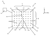
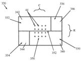
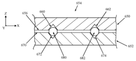
본 개시의 원리들에 따른 타일링된 디스플레이(20)의 일 실시예가 도 1에 간략화된 형태로 도시된다. 본 개시의 타일링된 디스플레이들은 일반적으로 둘 이상의 타일들, 예컨대 도 1에서 확인되는 제1 및 제2 타일들(30, 32)을 포함한다. 보다 상세히 아래에서 설명될 바와 같이, 각각의 타일들(30, 32)은 하나 이상의 픽셀들 또는 픽셀 요소들(44)을 수반하는 기판(40, 42)을 각각 포함한다. 상기 타일들(30, 32)은 상기 타일링된 디스플레이(20)의 최종 조립 시 픽셀 배열(46)이 형성되도록 서로에 대하여 배열되며, 상기 배열(46)의 상기 픽셀들(44)은 전체적으로 두 선형 방향들로, 예컨대 복수의 행들(R) 및 복수의 행들(R)에 수직한 복수의 열들(C)로 배열 또는 정렬된다. 대안적으로, 픽셀 배열은 다른 선형 방향들, 예컨대 복수의 행들 및 상기 행들에 수직하지 않은 복수의 대각선들에 의해 정의될 수 있다. 픽셀 피치는 상기 배열(46)에 의해 성립되며, "픽셀 피치"는 상기 배열(46)의 소정의 선형 방향으로 이웃한 또는 바로 인접한 픽셀들(44) 사이의 중심간 공칭(nominal) 또는 평균 거리(예를 들어, 각각의 행(R)의 방향으로(또는 방향을 따라) 이웃한 픽셀들(44)의 모든 쌍들 사이의 공칭 또는 평균 중심간 거리, 또는 각각의 열(C)의 방향으로(또는 방향을 따라) 이웃한 픽셀들(44)의 모든 쌍들 사이의 공칭 또는 평균 중심간 거리)로 정의된다. 소정의 선형 방향으로 이웃한 픽셀들(440)의 임의의 특정 쌍 사이의 실제 중심간 거리는 소정의 픽셀 피치로부터 다소 벗어나거나 변동될 수 있다는 것이 이해될 것이다; 그러나, 상기 배열(46)은 균일한 픽셀 피치를 가지는 것으로 특징지어지며, 여기서 "균일한 픽셀 피치"는 소정의 픽셀 피치(즉, 소정의 선형 방향으로 이웃한 픽셀들(44)의 모든 쌍들의 공칭 또는 평균 픽셀 피치)로부터 50% 이하, 대안적으로 40% 이하, 대안적으로 30% 이하, 대안적으로 20% 이하, 대안적으로 10% 이하, 대안적으로 5% 이하, 및 일부 실시예들에서 1% 이하로 벗어나거나 변동하는 소정의 선형 방향으로 이웃한 픽셀들(44)의 임의의 특정 쌍 사이의 중심간 거리로 정의된다. 본 개시의 일부 실시예들에서, 상기 기판들(40, 42)은 픽셀 피치들이 타일들(30, 32) 사이에 형성된 경계(seam)(50)에 걸쳐 유지되도록 또는 원하는 타일간 레지스트레이션(registration)(예를 들어, 픽셀 피치의 50% 이하의 레지스트레이션 오차, 대안적으로 40% 이하, 대안적으로 30% 이하, 대안적으로 20% 이하, 대안적으로 10% 이하, 대안적으로 5% 이하, 및 일부 실시예들에서 1% 이하), 또는 둘 모두를 촉진하는 하나 이상의 상보적인 형상들을 포함한다. 예를 들어, 상기 상보적인 형상(들)은 상기 경계(50)의 적어도 일부가 행들(R)의 방향에 비스듬하게 되도록 형성하는 방식으로 형상화되며 및/또는 상기 기판들(40, 42) 중 하나 또는 둘 모두의 엣지(들)이 깊이(Z) 방향으로 셩형된 상기 기판들(40, 42)을 포함할 수 있다. 참고로, 상기 타일링된 디스플레이(20)는 각각의 타일들(30, 32)에 전기적으로 연결되며 당업계에 알려진 바와 같이 좌표화된 이미지들을 디스플레이할 때 상기 타일들(30, 32)의 동작을 구동하도록 프로그래밍된 제어기(54)를 더 포함하는 디스플레이 장치(52)의 일부일 수 있다.One embodiment of a
본 개시의 타일들은 현재 알려진 또는 미래에 개발될 임의의 디스플레이 기술, 예컨대, 예를 들어 인광(phosphorescnet), 전장 발광(electroluminescent), 유기 또는 무기 발광, 투과, 반사 또는 다른 알려진 기술들을 포함할 수 있다. 따라서, 각각의 상기 타일들(30, 32)의 픽셀들(44)은 예를 들어 마이크로-LED들, LCD, OLED들, LED들, 전자 종이 등에 의해 제공될 수 있다. 디스플레이 기술들의 결합, 예컨대 LCD 장치 내에 사용되는 타일링된 마이크로-LED 배면광이 대안적으로 사용될 수 있다. 이러한 비제한적 예에서, 상기 마이크로-LED 배면광 배열의 픽셀 피치는 결합된 LCD의 픽셀 피치와 상이할 수 있다. 디지털 이미징에서, 픽셀은 래스터(raster) 이미지에서 물리적인 점이거나 디스플레이 장치 내의 가장 작은 어드레스 가능한(addressable) 디스플레이 구성 요소라는 것이 이해될 것이다; 다시 말해 픽셀은 상기 디스플레이 상에 표현되는 이미지 또는 그림의 가장 작은 제어 가능한 요소이다. 픽셀의 어드레스는 그 물리적 좌표들에 대응한다. 예컨대 LED 및 마이크로-LED와 같은 일부 디스플레이 기술들에서, 상기 픽셀(44)은 실제적으로 3개(이상)의 "서브-픽셀들"로 구성된 표면-실장 램프일 수 있으며, 그 각각은 적색, 녹색 및 청색 요소들(예를 들어, 다이오드들 또는 색 변환)을 포함하는 개별 LED(또는 마이크로-LED)이다. 예컨대 LCD와 같은 다른 디스플레이 기술들에서, 각각의 픽셀은 편광 필터들 및 적색, 녹색 및 청색 서브-픽셀들을 생성할 수 있는 색 필터들과 함께 두 투명 전극들 사이에 정렬된 분자들의 층으로 구성된다. 일부 실시예들에서, 본 개시의 타일들(예컨대 타일들(30, 32)) 및 따라서 타일링된 디스플레이(20)의 픽셀 피치의 공칭 값은 1.0mm 이하, 대안적으로 0.5mm 이하, 대안적으로 0.4mm 이하, 대안적으로 0.3mm 이하, 대안적으로 0.2mm 이하이며, 일부 실시예들에서(예를 들어 일부 마이크로-LED 디스플레이 기술들에서) 0.1mm 이하이다. 발광 디스플레이 기술이 사용되는 경우, 타일들(30, 32)은 전면 발광 또는 배면 발광 구조를 가질 수 있다. 또한, 상기 타일들(30, 32)은 전면 발광 또는 배면 발광 영역들 또는 혼합된 배열들을 가질 수 있다.Tiles of the present disclosure may include any display technology currently known or developed in the future, such as, for example, phosphororescnet, electroluminescent, organic or inorganic light emitting, transmissive, reflective or other known technologies. . Thus, the
상기를 유념하면서, 각각의 타일들(30, 32)에 구비된 상기 기판(40, 42)은 사용된 특정한 디스플레이 기술에 따라 다양한 형태들을 나타낼 수 있으며 다양한 기능들을 수행할 수 있다. 예를 들어, 일부 실시예들에서, 상기 기판(40, 42)은 픽셀 요소들(예를 들어, LED들, 마이크로-LED들 등)이 실장되거나 부착되는 표면을 제공할 수 있다. 다른 실시예들에서, 상기 기판(40, 42)은 디스플레이 기술 빌드-업의 필수 서브-구성일 수 있다(예를 들어, 전형적인 LCD 디스플레이 기술 빌드-업은 전면 플레이트, 결정 층, 배면 플레이트, 편광기, 광 분산기 및 배면 광원을 포함하고; 이러한 비제한적 예들에서, 상기 기판(40, 42)은 상기 전면 플레이트, 상기 후면 플레이트, 또는 상기 배면 광원 및 동일한 방식으로 또는 전혀 타일링되지 않은 다른 서브-구성들(또는 그 일부)로서 기능하도록 형성 및 구성될 수 있다. 대안적으로, 상기 기판(40, 42)은 특정 디스플레이 기술(예를 들어, LCD)에 유용한 박막 트랜지스터(thin-film transistor, TFT) 구성의 지지 층일 수 있다. 다른 실시예들에서, 상기 기판(40, 42)은 커버 플레이트일 수 있거나, 사용되는 디스플레이 기술의 통상적인 구성에 추가되는 구성 등일 수 있다. 이러한 개괄적인 설명들을 하면서, 일부 실시예들에서 상기 기판(40, 42)은 적어도 하나의 재료가 유리, 유리 세라믹 또는 세라믹인 단일, 다층, 또는 복합 구조일 수 있다. 상기 기판(40)은 특정한 디스플레이 기술에 따라 투명하거나, 산란적이거나 또는 불투명할 수 있다. 일부 실시예들에서, 상기 기판은 치수적으로 안정하도록 구성되며, 예를 들어 10 ppm/℃ 이하, 대안적으로 8 ppm/℃ 이하, 대안적으로 6 ppm/℃ 이하, 및 대안적으로 4 ppm/℃ 이하의 열 팽창 계수(coefficient of thermal expansion, CTE)를 나타낸다. 선택적으로, 상기 기판(40, 42)의 영률은 50GPa 이상, 대안적으로 60GPa 이상, 및 대안적으로 70GPa 이상이다. 상기 기판(40)의 선택적인 치수 안정성은 대안적으로 상기 기판(40)이 물 또는 용매의 존재 하에서 낮은 치수 변화를 겪도록 구성되는 것에 의해 특징지어질 수 있다 (즉 상기 기판이 물 또는 용매의 존재 하에서 10% 미만의 치수 변화를 경험한다). 일부 실시예들에서, 상기 기판(40, 42)은 2mm 이하, 대안적으로 1mm 이하, 대안적으로 0.7mm 이하, 대안적으로 0.5mm 이하, 대안적으로 0.3mm 이하, 및 대안적으로 0.2mm 이하의 두께를 가진다. 상기 기판들(40, 42)은 각각 0.05m 이상, 대안적으로 0.1m 이상, 대안적으로 0.5m 이상, 및 다른 실시예들에서 1m 이상의 적어도 하나의 선형 치수를 가질 수 있다. 일부 실시예들에서, 디스플레이 기술 적용 요건들에 따라, 상기 기판(40, 42)의 조성은 예를 들어 일부 TFT 제조 또는 이온-교환 공정들과 양립가능하도록 각각 실질적으로 알칼리가 없거나(즉, 1% 이하의 알칼리) 알칼리를 함유할 수 있다.With the above in mind, the
기판 형상Board Shape
위에 언급된 바와 같이, 일부 실시예들에서, 타일링된 디스플레이에 포함되는 둘 이상의 타일들(예컨대 타일들(30, 32))은 경계(50)에 걸쳐 균일한 픽셀 피치를 유지하는 것 및/또는 상기 픽셀 피치의 50% 이하, 대안적으로 40% 이하, 대안적으로 30% 이하, 대안적으로 20% 이하, 대안적으로 10% 이하, 대안적으로 5% 이하, 및 일부 실시예들에서 1% 이하의 오차로 타일간 레지트레이션을 촉진하는 상보적-형상의 기판들(예컨대 기판들(40, 42)) 및 픽셀 배열들을 포함할 수 있다. 추가적인 참고로서, 도 2a 및 도 2b는 도 1의 좌표 시스템에 따라 분리된 상태의 상기 제1 타일(30)을 도시한다. 도 2a 및 도 2b의 비제한적 실시예는 각각의 픽셀들(44)이 하나(또는 이상)의 마이크로-LED들에 의해 정의되는 가능한 마이크로-LED 디스플레이 구조 구성과 유사할 수 있다. 상기 픽셀들(44)은 상기 기판(40)의 표면 상에 배열되며, 상기 기판(40)은 상기 타일(30)의 최외곽 경계 또는 둘레를 정의한다. 상기 타일(30)은 상기 픽셀들(440)을 원하는 방식으로 동작시키기에 적합한 하나 이상의 추가적인 구성들, 예컨대 회로 트레이스들(circuitry traces), 또는 커넥터들(상기 기판(40) 상, 내, 또는 상기 기판(40)을 관통하여 형성될 수 있거나 형성되지 않을 수 있음), 커버 시트, 편광기들 등을 포함할 수 있다는 것이 이해될 것이다. 여하튼, 상기 기판(40)은 대향하는, 제1 및 제2 주면들(main surfaces)(60, 62)을 정의하는 것으로 보여질 수 있다. 상기 주면들(60, 62) 중 하나 또는 둘 모두는 X-Y(또는 디스플레이) 평면에서 실질적으로 평평하거나 평면(즉, 상기 타일(30)에 걸쳐 완전히 평평한 표면의 5% 내)일 수 있으며, 상기 기판(40)의 엣지들은 상기 Z 또는 깊이 방향으로 상기 주면들(60, 62) 사이에 연장될 수 있다. 예를 들어, 제1, 제2, 제3 및 제4 엣지들(64, 66, 68, 70)은 도 2a에서 확인되며, 상기 제1, 제2, 및 제3 엣지들(64, 66, 68)은 도 2b에서 볼 수 있다. 상기 픽셀들(44)은 상기 제1 주면(60) 상에 위치될 수 있으며, 균일한 픽셀 피치를 가지는 행렬(80)로 배열된다 (즉, 소정의 선형 방향(예를 들어, X 방향 및/또는 Y 방향)으로 이웃한 픽셀들(44) 사이의 중심간 거리는 위에 정의된 바와 같이 상기 행렬(80)에 걸쳐 균일하다). 상기 X 방향 및 상기 Y 방향으로의 픽셀 피치는 동일하거나 상이할 수 있다. 또한, 상기 픽셀 행렬(80)은 비직교 선형 방향들, 예컨대 상기 X 방향과 대각 방향에 의해 정의될 수 있다.As mentioned above, in some embodiments, two or more tiles (eg,
상기 엣지들(64, 66, 68, 70)은 결합되어 상기 기판(40)의 형상(X-Y 평면 내의)을 정의하며, 일부 실시예들에서, 상기 엣지들(64, 66, 68, 70) 중 적어도 하나의 적어도 일부는 비선형적이다. 예를 들어, 도 2a의 비제한적 실시예에서, 상기 X-Y 평면 내에서 상기 제1 엣지(64)는 비선형적인(예를 들어, 굽거나 물결 모양이다). 반면, 상기 제2, 제3, 및 제4 엣지들(66, 68, 70)은 선형적이다. 이러한 구성에서, 상기 비선형 제1 엣지(64)에 가장 인접한 상기 행렬(80)의 둘 이상의 픽셀들(44)(예를 들어, 도 2a에서 44a-44g로 식별되는 픽셀들)은 상기 제1 엣지(64)로부터 상이한 거리들에 위치된다. 예를 들어, 상기 제1 픽셀(44a)과 상기 비선형 제1 엣지(64) 사이의 거리는 상기 제5 픽셀(44e)과 상기 비선형 제1 엣지(64) 사이의 거리보다 크다. 본 개시의 일부 실시예들에서, 하나 이상의 픽셀들(44)은 상기 기판(40)의 엣지에 매우 가깝게 위치될 수 있다(예를 들어, 0.3mm 이하, 대안적으로 0.2mm 이하, 및 대안적으로 0.1mm 이하의 거리 또는 간격). 여하튼, 상기 타일링된 디스플레이(20)(도 1)의 하나 이상의 다른 타일들은 상기 비선형 제1 엣지(64)의 형상 및 상기 비선형 제1 엣지(64)에 대하여 상기 행렬(80)의 상기 픽셀들(440)의 위치를 보완하는 형상들을 포함할 수 있다. The
예를 들어, 도 1을 추가적으로 참조하면, 상기 제2 타일(32)의 상기 기판(42)은 위에 설명된 상기 제1 타일(30)의 상기 기판(40)과 매우 유사할 수 있다. 상기 타일링된 디스플레이(20)의 최종 조립 시, 상기 제1 타일(30)의 상기 기판(40)의 상기 제1 엣지(64)는 상기 제2 타일(320)의 상기 기판(42)의 제1 엣지(90)와 대면하여 상기 경계(50)를 형성한다. 상기 제2 타일 기판(42)의 상기 제1 엣지(90)는 X-Y 평면 내에서 상기 제1 타일 기판(40)의 상기 제1 엣지(64)의 형상을 보완하거나 모방하는 비선형 형상을 가진다. 또한, 상기 제2 타일(32)의 상기 픽셀들(44)은 상기 제1 타일(30)과 동일한 균일한 픽셀 피치를 가지는 행렬(92)로 배열되며, 상기 행렬(92)은 상기 대응하는 제1 엣지(64)에 대한 상기 제1 타일(30)의 상기 픽셀 행렬(90)의 정렬과 대응하는 방식으로 상기 제1 엣지(90)에 대하여 정렬된다(상기 제1 타일 픽셀 행렬(80)과 상기 제2 타일 픽셀 행렬(92)은 결합하여 상기 타일링된 디스플레이(20)의 상기 픽셀 배열(46)을 생성한다는 것이 이해된다). 이러한 구성에서, 상기 상보적인 비선형 제1 엣지들(64, 90)은 서로에 대하여 상기 제1 및 제2 타일들(30, 32)의 쉽고 일관된 배열 및 레지스트레이션을 용이하게한다(예를 들어, 상기 제1 타일 기판(40)의 상기 제1 엣지(64)는 쉽게 상기 제2 타일 기판(42)의 상기 제1 엣지(90)와 "일치" 또는 짝지어진다). 결과적인 상기 경계(50)는 상기 상보적인 제1 엣지들(64, 90)의 비선형적 형상을 모방한다. 이와 관련하여, 선택적인 비선형 형상의 경계(50)는 광범위한 다른 형상들을 나타낼 수 있으며, 상기 경계(50)의 일부는 선형일 수 있다. 보다 일반적인 용어들로, 본 개시의 일부 실시예들에서, 이웃한 타일들의 엣지들을 대면시킴으로써 형성된 상기 경계(50)는 상기 픽셀 배열(46)의 복수의 행들(R)에 대하여 비스듬한 적어도 일부를 포함하는 것으로 설명될 수 있다. 다른 실시예들에서, 그러나, 상기 경계의 전체는 상기 행들(R)에 평행하거나 수직할 수 있다. 이러한 비제한적 예에서, 상기 타일 엣지들(64, 90)은 서로와 물리적으로 접촉하거나 접촉하지 않을 수 있다.For example, referring further to FIG. 1, the
상기 타일들(30, 32)은 최종 조립시 상기 타일들(30, 32)의 균일한 픽셀 피치가 상기 경계(50)에 걸쳐 유지되도록 더 구성된다. 달리 말해, 상기 경계(50)의 반대 측들에 정렬된 픽셀들 사이의 중심간 간격은 상기 개별 타일들(30, 32) 내에 형성된 균일한 픽셀 피치에 대응한다(즉 10% 이내). 따라서, 예를 들어, 최종 조립 시, 상기 제1 타일(30)의 상기 제1 픽셀(44a)은 상기 제2 타일(32)의 제1 픽셀(44a')과 정렬되고, 상기 제1 타일(30)의 상기 제5 픽셀(44e)은 상기 제2 타일(32)의 제5 픽셀(44e')과 정렬된다. 상기 제1 타일(30)의 상기 제1 픽셀(44a)과 대응하는 제1 엣지(64) 사이의 거리는 상기 제5 픽셀(44e)의 그것보다 크나, 상기 제1 및 제5 픽셀들(44a', 44e')은 대응하는 제1 엣지(90)에 대하여 반대의 관계를 가진다. 따라서, 최종 조립 시, 상기 이웃하지만 상기 경계(50)의 반대 측들에 위치하는 제1 픽셀들(44a, 44a') 사이의 상기 중심간 거리는 이웃한 제5 픽셀들(44e, 44e') 사이의 줌심간 거리와 마찬가지로 균일한 픽셀 피치에 대응하거나 이를 유지한다.The
상기 타일링된 디스플레이의 두 이웃한 타일들이 상보적인 비선형적 엣지들을 포함하는 실시예들에서(예컨대 도 1의 비제한적인 예시적인 타일들(30, 32)에서), 대응하는 기판들(40, 42)은 비선형성이 상기 픽셀 피치 간격 내에 포함되고 서로-맞물리는(inter-digitated) 픽셀들을 생성하지 않도록 구성될 수 있다. 즉, 상기 제1 엣지들(64, 90) 내의 어떠한 비선형성(또는 선형성으로부터 벗어남)도 픽셀 피치(공칭 값 또는 평균)보다 작다. 이러한 선택적인 특징은 대안적으로 예를 들어 상기 경계(50)에 가장 근접한 하나 이상의 픽셀들(44)을 참조하여 설명될 수 있다. 예를 들어, 도 1의 구성에서, 상기 제1 타일(30)의 상기 제5 픽셀(44e)은 대응하는 상기 제1 엣지(64)(및 따라서 상기 경계(50))에 가장 근접한 상기 제1 타일 픽셀이다. 결과적인 타일링된 디스플레이(30)의 상기 픽셀 배열(46)에서, 상기 제1 타일(30)의 상기 제5 픽셀(44e)은 제1 행(R1) 및 제1 열(C)과 정렬된다. 위에 언급된 서로-맞물리는 픽셀들의 부존재는 상기 제2 타일(32)의 상기 픽셀들(44)이 상기 제1 행(R1) 또는 상기 제1 열(C1)을 따라 상기 제1 타일(30)의 상기 픽셀들(44) 사이에 개재되지 않는다는 것을 의미한다. 이러한 선택적인 구성에서, 상기 기판 엣지 비선형성은 비교적 상당하지 않으며 취급 동안 기판 손상 또는 파손의 가능성을 최소화한다 (예를 들어, 상당한 비선형성이 상기 기판 엣지에 의해 형성되는 경우, 상기 기판의 비선형 영역은 취급동안 쉽게 손상되거나 파손될 것이다). In embodiments where two neighboring tiles of the tiled display include complementary nonlinear edges (eg, in the non-limiting
도 1의 상기 타일링된 디스플레이(20)는 두 개의 타일들(30, 32)을 포함하는 것으로 설명되었으나, 다른 실시예들에서, 셋 이상의 타일들이 제공될 수 있다. 또한, 하나 이상의 타일 기판들(40, 42)의 들 이상의 엣지는 위에 설명된 비선형적인 형상을 포함할 수 있다; 상기 타일링된 디스플레이에 포함되는 타일들은 동일한 형상 또는 치수를 가지거나 가지지 않을 수 있다. 타일간 경계를 향하는 선형 방향으로의 픽셀 피치는 대안적인 선형 방향으로의 픽셀 피치와 상이할 수 있다.Although the
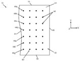
상기 비선형 엣지(들)은 본 개시의 원리들에 따른 상보적 형상 피쳐(feature)의 비제한적 예이다. 다른 실시예들에서, 상기 타일 기판들은 경계에 걸쳐 픽셀 피치를 유지하고 유익한 타일간 레지스트레이션을 제공하는 한편 선형 경계와 접경하도록 구성 및 형상화될 수 있다. 예를 들어, 본 개시의 타일링된 디스플레이(120)의 다른 실시예가 도 3에 간략화된 형태로 도시되며 복수의 타일들, 예컨대 제1, 제2, 제3, 제4, 제5, 제6, 및 제7 타일들(130, 132, 134, 136, 138, 140, 142)을 포함한다. 상기 타일들(130 내지 142) 각각은 위의 설명과 일관된 기판, 예컨대 상기 제1, 제2 및 제3 타일들(130, 132, 134)의 경우 각각 도 3에서 확인되는 기판들(150, 152, 154)을 포함한다. 타일들(130-142)은 이전에 설명된 임의의 디스플레이 기술들을 복수의 픽셀들 또는 픽셀 요소들(44)을 수반하는 대응하는 기판(예를 들어, 기판들(150-154))에 통합할 수 있다. 참고로, 설명의 편의를 위하여, 제6 및 제7 타일들(140, 142)에 픽셀들이 도시되지 않는다; 일부 실시예들에서, 본 개시의 타일링된 디스플레이들의 타일들 중 일부만이 픽셀들을 포함한다. 무관하게, 상기 픽셀들(44)은 상기 타일링된 디스플레이(120)의 최종 조립 시 배열(150)로 전체적으로 배열되며, 상기 배열(160)은 위에 설명된 바와 같이 각각 동일한, 균일한 픽셀 피치를 가지는 복수의 행들(R) 및 열들(C)을 포함한다. 두(또는 그 이상의) 이웃하는 타일들(130-142)은 그들 사이에 형성된 경계에 걸쳐 픽셀 피치를 유지하는 상보적인 형상 피쳐들 및 픽셀 배열들을 가진다. 상기 배열(160)의 균일한 픽셀 피치는 대안적인 선형 방향으로의 픽셀 피치 값과 동일하거나 상이한 하나의 선형 방향으로의 픽셀 피치 값일 수 있다.The non-linear edge (s) are non-limiting examples of complementary shape features in accordance with the principles of the present disclosure. In other embodiments, the tile substrates can be constructed and shaped to border the linear boundary while maintaining pixel pitch across the boundary and providing beneficial inter-tile registration. For example, another embodiment of a
예를 들어, 상기 제1 및 제2 타일 기판들(150, 152)은 최종 조립시 그들 사이에 제1 경계(162)를 정의하도록 상보적인 형상들을 가진다. 특히, 상기 제1 및 제2 타일 기판들(150, 152)은 최종 조립 시 상기 제1 타일 기판(150)의 제1 엣지(170)가 상기 제2 타일 기판(152)의 제1 엣지(180)를 보완 및 대면하여 상기 제1 경계(162)를 형성하도록 치수 및 형상을 가진다. 상기 엣지들(170, 180)은 서로 물리적인 접촉을 하거나 하지 않을 수 있다. 상기 제1 타일(130)의 픽셀들(44)은 상기 제1 타일 기판(150)에 행렬로 배열되며, 상기 제1 타일(130)의 상기 픽셀 행렬은 균일한 픽셀 피치를 가진다. 상기 제2 타일(132)의 상기 픽셀들(44)은 또한 균일한 픽셀 피치로 상기 제2 타일 기판(152)에 행렬로 배열된다. 상기 제1 및 제2 타일들(130, 132) 각각의 상기 픽셀들(44)의 각각 대응하는 기판 제1 엣지(170, 180)에 대한 상보적인 관계가 또한 제공된다. 이러한 상보적인 형상들 및 픽셀 배열들에서, 상기 제1 경계(162)의 반대 측들에서 이웃하는 픽셀들(44) 사이의 픽셀 피치는 타일들(130, 132)(및 따라서 타일링된 디스플레이(120)의 픽셀 배열(160))의 균일한 픽셀 피치에 대응한다. 예를 들어, 상기 제1 타일(130)의 상기 픽셀들(44)은 상기 제1 엣지(180)에 인접한 제1 및 제2 픽셀들(44a, 44b)을 포함한다. 상기 제2 타일의 픽셀들(44)은 제1 및 제2 픽셀들(44a, 44b)을 포함한다. 상기 제2 타일의 상기 픽셀들(44)은 제1 및 제2 픽셀들(44a', 44b')을 포함한다. 최종 조립 시, 상기 제1 타일(130)의 상기 제1 픽셀(44a)은 상기 제2 타일(132)의 상기 제1 픽셀(44a')(열들(C) 중 하나의 일부로서) 및 상기 제2 픽셀(44b')(행들(R) 중 하나의 일부로서)과 레지스터된다. 상기 제1 타일(130)의 상기 제1 픽셀(44a)과 상기 제2 타일(132)의 상기 제1 픽셀(44a') 사이의 중심간 거리(열 방향으로의)는 상기 제1 타일(130)의 상기 제1 픽셀(44a)과 상기 제2 타일(132)의 상기 제2 픽셀(44b') 사이의 중심간 거리(행 방향으로의)와 마찬가지로 균일한 픽셀 피치에 대응한다. 유사하게, 상기 제1 타일(130)의 상기 제2 픽셀(44b)과 상기 제2 타일(132)의 상기 제2 픽셀(44b') 사이의 중심간 거리(열 방향으로의)는 균일한 픽셀 피치와 대응한다. 유사한 관계가 최종 조립 시 상기 제1 타일 기판(150)의 엣지와 상기 제3 타일 기판(154)의 엣지 사이에 정의되는 제2 경계(164)(즉, 상기 제2 경계(164)에 걸친 상기 제1 및 제3 타일들(130, 134)의 이웃한 픽셀들(44) 사이의 중심간 거리들은 균일한 픽셀 피치와 대응하며), 및 상기 타일 디스플레이(120)의 다른 경계들(예를 들어, 상기 제2 타일 기판(152)의 엣지와 상기 제3 타일 기판(154)의 엣지 사이에 정의되는 제3 경계(166))에 걸쳐 성립된다.For example, the first and
이전의 실시예들 처럼, 적어도 두 타일 기판들의 상보적인 형상들은 대응하는 경계의 적어도 일부를 행들(R)에 비스듬하게 배향시킨다. 예를 들어, 상기 제1 경계(162) 전체 및 상기 제2 경계(164) 전체는 행들(R)에 비스듬하다(상기 타일링된 디스플레이(120)의 다른 경계들, 예를 들어, 상기 제3 경계(166)는 행들(R)과 수직하거나 평행할 수 있다는 것이 이해될 것이다). 또한, 최종 조립 시, 이웃하는 타일들의 픽셀들(44)은 서로-맞물리지 않는다(예를 들어, 상기 제2, 제3, 및 제4 타일들(132, 134, 136)의 픽셀들(44)은 임의의 상기 열들(C) 또는 행들(R)의 상기 제1 타일(130)의 픽셀들 사이에 개재되지 않는다). 또한, 경계들 중 일부는 상호 교차하나(예를 들어, 상기 제1, 제2, 및 제3 경계들(162, 164, 166)은 서로 교차하나), 상기 타일링된 디스플레이(120)의 교차하는 경계들 중 어느 것도 행들(R) 또는 열들(C)과 평행한 연속적인 선형 경계 또는 선을 형성하지 않는다. 이러한 선택적인 배열은 개별적인 타일들(130-136)이 시간에 걸쳐 서로에 대하여 이동할 가능성을 낮춤으로써 상기 타일링된 디스플레이(120)의 전체적인 기계적 안정성을 향상시킬 수 있다.As in the previous embodiments, the complementary shapes of the at least two tile substrates orient the at least a portion of the corresponding boundary obliquely to the rows R. FIG. For example, the entirety of the
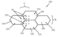
도 3의 상기 기판 형상들(및 대응하는 픽셀 배열들)은 본 개시의 원리들에 따른 비제한적인 예들이다. 다른 실시예들에서, 상기 타일 기판들은 다수의 다른 둘레 형상들, 예컨대 직사각형, 육각형, 삼각형, 또는 타일링된 디스플레이를 형성하도록 서로에 대하여 조립되었을 때 픽셀 배열 내에 공극을 남기지 않는 임의의 다른 단위 형상들을 가질 수 있다. 전체적으로 조립된 타일링된 디스플레이 내의 개별적인 타일들 모두는 동일한 형상 또는 치수를 가질 필요가 없으나, 일부 실시예들에서 동일한 형상을 가진다. 이에 유념하면서, 타일링된 디스플레이(220)의 다른 비제한적 실시예가 도 4에 간략화된 형태로 도시된다. 상기 타일링된 디스플레이(220)는 위의 설명들과 유사할 수 있으며, 복수의 타일들, 예컨대 제1, 제2, 제3, 및 제4 타일들(230, 232, 234, 236)을 포함한다. 상기 타일들(230-236) 각각은 위의 설명들과 일관된 기판, 예컨대 기판들(240, 242, 244, 246)을 각각 포함한다. 상기 타일들(230 내지 236)은 위에 설명된 임의의 디스플레이 기술들을 복수의 픽셀들 또는 픽셀 요소들(44)을 수반하는 일부 또는 전부의 대응하는 기판들(240 내지 246)에 통합할 수 있다. 설명의 편의를 위하여, 픽셀들(44)은 제4 타일(236)에 도시되지 않았다. 상기 픽셀들(44)은 위에서 설명된 바와 같이 상기 타일링된 디스플레이(220)의 최종 조립 시 전체적으로 배열(250)로 배열되며, 상기 배열(250)은 복수의 행들(R) 및 열들(C)을 포함하며, 각각은 동일한, 균일한 픽셀 피치를 가진다. 행들(R) 내의 픽셀 피치는 열들(C) 내의 픽셀 피치와 동일하거나 상이할 수 있다. 두(또는 그 이상) 이웃한 타일들(230 내지 236)은 그들 사이에 형성된 경계에 걸쳐 픽셀 피치를 유지하는 상보적인 형상 피쳐들 및 픽셀 배열들을 가진다.The substrate shapes (and corresponding pixel arrangements) of FIG. 3 are non-limiting examples in accordance with the principles of the present disclosure. In other embodiments, the tile substrates may have a number of other circumferential shapes, such as rectangular, hexagonal, triangular, or any other unit shapes that do not leave voids in the pixel arrangement when assembled with each other to form a tiled display. Can have All of the individual tiles in the overall assembled tiled display need not have the same shape or dimensions, but in some embodiments have the same shape. With this in mind, another non-limiting embodiment of
예를 들어, 상기 제1 및 제2 타일 기판들(240, 242)은 최종 조립 시 그들 사이에 제1 경계(252)를 정의하도록 상보적인 형상들을 가진다. 상기 제1 경계(252)는 행들(R)에 비스듬하다. 또한, 위의 설명과 상응하게, 상기 제1 및 제2 타일들(230, 232)(예를 들어, 기판 형상 및 픽셀 배열)은 상기 제1 경계(252)에 걸친 픽셀 피치(행들(R)의 방향으로의 및 상기 열들(C)의 방향으로의)가 각각의 개별적인 타일(230, 232)(및 따라서 상기 타일링된 디스플레이(220))의 균일한 픽셀 피치와 대응하고, 상기 제1 타일(230)의 상기 픽셀들(44)과 상기 제2 타일(232)의 픽셀들(44)이 서로에 대하여 레지스터되도록(예를 들어, 소정의 선형 방향으로의 픽셀 피치의 50% 이하, 대안적으로 40% 이하, 대안적으로 30% 이하, 대안적으로 20% 이하, 대안적으로 10% 이하, 대안적으로 5% 이하, 및 일부 실시예들에서 1% 이하의 레지스트레이션 오차) 구성된다. 유사한 관계들이 상기 타일링된 디스플레이(220)의 다른 경계들에서 성립된다. 또한, 경계들 중 일부가 교차하나, 상기 타일링된 디스플레이(220)의 상기 교차하는 경계들 중 어느 것도 상기 행들(R) 또는 상기 열들(C)과 평행한 연속적인 선형 경계 또는 선을 형성하지 않는다. For example, the first and
타일링된 디스플레이(320)의 다른 비제한적 실시예가 간략화된 형태로 도 5에 도시된다. 상기 타일링된 디스플레이(320)는 위의 설명과 유사할 수 있으며, 복수의 타일들, 예컨대 제1, 제2, 제3, 및 제4 타일들(330, 332, 334, 336)을 포함한다. 상기 타일들(330 내지 336) 각각은 위의 설명들과 일관된 기판, 예컨대 기판들(340, 342, 344, 346)을 각각 포함한다. 상기 타일들(330 내지 336)은 이전에 설명된 임의의 디스플레이 기술들을 복수의 픽셀들 또는 픽셀 요소들(44)을 수반하는 대응하는 일부 또는 전부의 기판들(340, 346)에 통합할 수 있다. 설명의 편의를 위하여, 상기 제3 및 제4 타일들(334, 336)에 픽셀들이 도시되지 않았다. 상기 픽셀들(44)은 상기 타일링된 디스플레이(320)의 최종 조립 시 전체적으로 배열(350)로 배열되며, 상기 배열(350)은 위에 설명된 바와 같이 각각이 동일한, 균일판 픽셀 피치를 가지는 복수의 행들(R) 및 열들(C)을 포함한다. 행들(R) 내의 픽셀 피치는 행들(C) 내의 픽셀 피치와 동일하거나 상이할 수 있다. 두(또는 그 이상의) 이웃한 타일들(330-336)은 그들 사이에 형성된 경계에 걸쳐 픽셀 피치를 유지하는 상보적인 형상 피쳐들 및 픽셀 배열들을 가진다.Another non-limiting embodiment of
예를 들어, 상기 제1 및 제2 타일 기판들(340, 342)은 최종 조립 시 그들 사이의 제1 경계(352)를 정의하도록 상보적인 형상들을 가진다. 위의 설명들과 상응하게, 상기 제1 및 제2 타일들(330, 332)(예를 들어, 기판 형상 및 픽셀 배열)은 상기 제1 경계(352)에 걸친 픽셀 피치(열들(C)의 방향으로의)가 각각의 개별적인 타일(330, 332)(및 따라서 상기 타일링된 디스플레이(320))의 균일한 픽셀 피치와 대응하고 상기 제1 타일(330)의 픽셀들(44)과 상기 제2 타일(3320)의 픽셀들(44)이 서로에 대하여 레지스터되도록(예를 들어, 균일한 픽셀 피치의 50% 이하의 레지스트레이션 오차) 구성된다. 유사한 관계들이 상기 타일링된 디스플레이(220)의 다른 경계들에 성림될 수 있다. 또한, 상기 경계들 중 일부가 교차하나, 상기 타일링된 디스플레이(320)의 교차하는 경계들 중 어느 것도 상기 열들(C)과 평행한 연속적인 선형 경계 또는 선을 형성하지 않는다.For example, the first and
위에 설명된 임의의 형상들은 특정 기판 재료(들)에 적합한 알려진 제조 기술들을 통해 대응하는 기판에 구현될 수 있다. 예를 들어, 원하는 기판 형상을 생성하는 방법들은 기계적 스크라이브(scribe), 레이저 절단, 식각, 열 성형 등을 포함할 수 있다. 또한, 설명된 기판 형상을 생성하기 위해 다수의 공정들이 사용될 수 있다. 예를 들어, 상기 기판은 처음에 기계적으로 스크라이브된 후 식각될 수 있다.Any of the shapes described above can be implemented on a corresponding substrate through known fabrication techniques suitable for the particular substrate material (s). For example, methods of producing the desired substrate shape may include mechanical scribe, laser cutting, etching, thermoforming, and the like. In addition, multiple processes can be used to create the described substrate shape. For example, the substrate can be initially etched after being mechanically scribed.
기판 엣지 프로파일Board Edge Profile
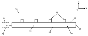
위에서 설명된 상기 기판 형상들에 추가적으로, 또는 그에 대한 대안으로서, 본 개시의 일부 실시예들에서, 상기 타일링된 디스플레이의 타일들 내에 포함된 상기 상보적인 형상들은 기판 엣지 프로파일을 포함할 수 있다. 도 2b를 참조하면, "엣지 프로파일"은 대향하는 주면들(60, 62) 사이에 연장되는 Z 또는 깊이 방향으로 하나 이상의 상기 기판 엣지들(64, 66, 68)의 형상과 관련된다. 도 2b의 도면의 시점에 대하여, 상기 엣지 프로파일은 상기 제1 및 제3 엣지들(64, 68)의 경우 가장 눈에 띄게 보이며, 상기 제1 주표면(60)의 주평면(P1) 및 상기 제2 주표면(62)의 주평면(P2)과 관련하여 설명될 수 있다 (일부 실시예들에서, 상기 주평면들(P1, P2)이 평행하다는 것이 이해될 것이다). 도 2b의 구성에서, 상기 제1 엣지(64)의 프로파일은 상기 깊이 방향(Z)으로 상기 제1 엣지(64)의 전체가 상기 주면들(60, 62)의 상기 주평면(P1, P2)에 수직한 것이다. 상기 제3 엣지(68)는 유사한(즉, 상기 깊이 방향(Z)으로 상기 주면들(60, 62)의 상기 주평면(P1, P2)에 전체적으로 수직한) 엣지 프로파일을 가진다.In addition to or as an alternative to the substrate shapes described above, in some embodiments of the present disclosure, the complementary shapes included in tiles of the tiled display may include a substrate edge profile. Referring to FIG. 2B, an “edge profile” relates to the shape of one or more of the substrate edges 64, 66, 68 in the Z or depth direction extending between opposing
위의 배경과 달리, 본 개시의 다른 실시예들에서, 상기 깊이 방향(Z)으로 상기 타일 기판의 적어도 하나의 엣지들의 프로파일의 적어도 일부는 주평면들(P1, P2) 중 하나 또는 둘 모두에 수직하지 않다(예를 들어, 완전히 수직한 관계로부터 적어도 2도, 대안적으로 적어도 3도, 대안적으로 적어도 5도, 및 일부 실시예들에서 적어도 10도의 벗어남). 예를 들어, 본 개시의 원리들에 따른 타일링된 디스플레이(400)의 다른 실시예의 부분들이 간략화된 형태로 도 6에 도시된다. 상기 타일링된 디스플레이(400)는 위의 설명들과 유사할 수 있으며, 복수의 타일들, 예컨대 제1 및 제2 타일들(410, 412)을 포함한다. 상기 타일들(410, 412) 각각은 위의 설명들과 일관된 기판, 예컨대 기판들(420, 422)을 각각 포함한다. 상기 타일들(410, 412)은 이전에 설명된 임의의 디스플레이 기술들을 복수의 픽셀들 또는 픽셀 요소들(44)을 수반하는 대응하는 기판들(420, 422)에 통합할 수 있다. 상기 픽셀들(44)은 상기 타일링된 디스플레이(400)의 최종 조립 시 전체적으로 위에 설명된 바와 같이 각각 균일한 픽셀 피치를 가지는 복수의 행들 및 열들을 포함하는 배열로 배열된다. 상기 행들 내의 상기 픽셀 피치는 상기 열들 내의 상기 픽셀 피치와 동일하거나 상이할 수 있다. 상기 이웃한 제1 및 제2 타일들(410, 412)은 그들 사이에 형성된 경계(424)에 걸쳐 균일한 픽셀 피치를 유지하는 상보적인 형상 피쳐들(예를 들어, 엣지 프로파일 피쳐들) 및 픽셀 배열들을 가진다.Unlike the background above, in other embodiments of the present disclosure, at least a portion of the profile of the at least one edge of the tile substrate in the depth direction Z is in one or both of the main planes P1, P2. Not perpendicular (eg, at least 2 degrees, alternatively at least 3 degrees, alternatively at least 5 degrees, and at least 10 degrees in some embodiments) from a completely vertical relationship. For example, portions of another embodiment of a
상기 제1 타일 기판(420)은 대향하는 제1 및 제2 주면들(430, 432) 및 상기 주면들(430, 432) 사이에 Z 또는 깊이 방향으로 연장되는 제1 엣지(434)를 정의한다. 대향하는 주면들(430, 432) 각각은 주평면(P1a, P2a)을 정의한다. 상기 제1 엣지(434)의 엣지 프로파일 전체가 상기 주평면들(P1a, P2a)에 수직하지 않다. 예를 들어, 상기 제1 엣지(434)와 상기 제1 주면(430)의 교차는 예각을 정의하고, 상기 제1 엣지(434)와 상기 제2 주면(432)의 교차는 둔각을 정의한다. 상기 제2 타일 기판(422)은 또한 대향하는 제1 및 제2 주면들(440, 442) 및상기 주면들(440, 442) 사이에 Z 또는 깊이 방향으로 연장되는 제1 엣지(444)를 정의한다. 대향하는 주면들(440, 442) 각각은 주평면(P1b, P2b)을 정의한다. 상기 제1 엣지(444)의 엣지 프로파일 전체는 상기 주평면들(P1b, P2b)에 수직하지 않다. 또한, 상기 제2 타일 제1 엣지(444)의 공간적 배향은 상기 제1 타일 제1 엣지(434)의 그것과 상보적이다. 예를 들어, 상기 제1 엣지(444)와 상기 제1 주면(440)의 교차는 둔각을 정의하고, 상기 제1 엣지(444)와 상기 제2 주면(442)의 교차는 예각을 정의한다. 도 6의 조립된 배열에서, 상기 제1 타일 제1 엣지(434)는 상기 제2 타일 제1 엣지(444)와 마주보며 경계(424)를 정의하고, 상기 제1 엣지들(434, 444)은 실질적으로 평행하다(즉, 완전히 평행한 관계의 5도 이내). 도 6의 방향에 대하여, 상기 제1 타일 제1 엣지(434)는 상기 제2 타일 제1 엣지(444) 위에 놓이는 것으로 보여질 수 있다.The
도 6은, 일부 실시예들에서, 상기 타일링된 디스플레이(400)의 최종 조립 시, 이웃하는 타일들(예컨대 상기 제1 및 제2 타일들(410, 412))이 서로 물리적으로 접촉하지 않는다(예를 들어, 상기 제1 타일 기판(420)과 상기 제2 타일 기판(422)은 서로로부터 물리적으로 분리되어 상기 경계(424)는 갭 또는 공간이다)는 것을 더 반영한다. 아래 설명된 바와 같이, 상기 갭 내로 재료가 배치 또는 충전될 수 있다. 다른 실시예들에서, 상기 타일들(410, 412)은 최종 조립 시 물리적으로 접촉한다. 여하튼, 상기 상보적인 엣지 프로파일들은 타일링된 디스플레이(400)의 균일한 픽셀 피치가 상기 경계(424)에 걸쳐 유지되도록 인접한 타일들(410, 412)의 상보적인 맞춤을 가능하게 한다. 상기 상보적인 엣지 프로파일들은 또한 이웃한 타일들(예를 들어, 상기 제1 타일 기판(420)과 상기 제2 타일 기판(422))의 상기 픽셀들(44) 및/또는 상기 기판들의 수직 정렬을 가능하게할 수 있다.FIG. 6 illustrates that in some embodiments, neighboring tiles (eg, the first and
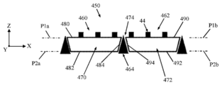
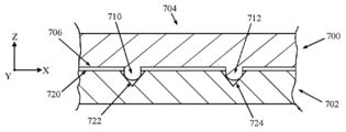
본 개시의 원리들에 따른 타일링된 디스플레이(450)의 다른 실시예의 부분들이 간략화된 형태로 도 7에 도시된다. 상기 타일링된 디스플레이(450)는 위의 설명들과 유사할 수 있으며, 복수의 타일들, 예컨대 제1 및 제2 타일들(460, 462) 및 하나 이상의 프레임 요소들, 예컨대 프레임 요소(464)를 포함한다. 상기 타일들(460, 462) 각각은 위의 설명들과 일관된 기판, 예컨대 기판들(470, 472)을 각각 포함한다. 상기 타일들(460, 462)은 이전에 설명된 임의의 디스플레이 기술들을 복수의 픽셀들 또는 픽셀 요소들(44)을 수반하는 대응하는 기판들(470, 472)에 통합할 수 있다. 상기 픽셀들(44)은 상기 타일링된 디스플레이(450)의 최종 조립 시 전체적으로 배열로 배열되며, 상기 배열은 위에서 설명된 바와 같이 균일한 픽셀 피치를 각각 가지는 복수의 행들 및 열들을 포함한다. 상기 행들 내의 상기 픽셀 피치는 상기 열들 내의 픽셀 피치와 동일하거나 상이할 수 있다. 이웃하는 제1 및 제2 타일들(460, 462)은 프레임 요소(들)(464)과 함께 그들 사이에 형성된 경계(474)(일반적으로 참조됨)에 걸쳐 균일한 픽셀 피치를 유지하는 상보적인 형상 피쳐들 및 픽셀 배열들을 가진다.Portions of another embodiment of a
상기 제1 타일 기판(470)은 대향하는 제1 및 제2 주면들(480, 482), 및 상기 주면들(480, 482) 사이에 Z 또는 깊이 방향으로 연장되는 제1 엣지(484)를 정의한다. 상기 대향하는 주면들(480, 482) 각각은 주평면(P1a, P2a)을 정의한다. 상기 제1 엣지(484)의 엣지 프로파일 전체는 상기 주평면들(P1a, P2a)에 수직하지 않다. 예를 들어, 상기 제1 엣지(484)와 상기 상기 제1 주면(480)의 교차는 예각을 정의하고, 상기 제1 엣지(484)와 상기 제2 주면(482)의 교차는 둔각을 정의한다. 상기 제2 타일 기판(472)은 또한 대향하는, 제1 및 제2 주면들(490, 492) 및 상기 주면들(490, 492) 사이에 상기 Z 또는 깊이 방향으로 연장되는 제1 엣지(494)를 정의한다. 상기 대향하는 주면들(490, 492) 각각은 주평면(P1b, P2b)을 정의한다. 상기 제1 엣지(494)의 엣지 프로파일의 전체는 상기 주평면들(P1b, P2b)에 수직하지 않다. 예를 들어, 상기 제1 엣지(494)와 상기 제1 주면(490)의 교차는 예각을 정의하고 상기 제1 엣지(494)와 상기 제2 주면(492)의 교차는 예각을 정의한다.The
상기 프레임 요소(464)는 상기 제1 엣지들(484, 494)의 상보적인 프로파일들에 따라 크기 및 형상을 가진다. 도 7의 조립된 배열에서, 상기 제1 타일 제1 엣지(484)는 상기 제2 타일 제1 엣지(494)를 마주보며 상기 경계(474)를 정의한다. 상기 프레임 요소(464)는 상기 경계(474) 내에 또는 상기 경계(474)를 따라 위치되며, 서로에 대하여 상기 제1 및 제2 타일들(460, 462)을 유지한다 (예를 들어, 상기 제1 및 제2 타일 기판들(470, 472)은 상기 프레임 요소(464)에 고정될 수 있다). 상기 상보적인 엣지 프로파일들, 상기 대응하는 제1 엣지(484, 494)에 대한 각각의 상기 타일들(460, 462)의 픽셀들(44)의 배치, 및 상기 프레임 요소(464)에 의해 지시되는 서로에 대한 엣지들(484, 494)의 공간적 배열은 결합하여 상기 경계(474)에 걸쳐 균일한 픽셀 피치를 유지한다(즉, 상기 경계(474)의 반대 측들에 소정의 선형 방향으로 이웃한 픽셀들(44) 사이의 중심간 거리는 각각의 상기 타일들(460, 462) 및 따라서 상기 타일링된 디스플레이(450)에 형성된 소정의 선형 방향으로의 균일한 픽셀 피치와 대응한다).The
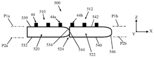
위에 언급된 바와 같이, 본 개시의 타일링된 디스플레이들은 선택적인 상보적인 기판 엣지 프로파일들을 포함할 수 있으며, 이웃한 타일들은 서로로부터 이격된다(예를 들어, 도 6 및 도 7의 비제한적 실시예들에서). 다른 실시예들에서, 상보적인 프로파일을 가지는 엣지들을 가지는 타일들은 최종 조립시 계면의 연장된 길이를 따라 또는 불연속적인 위치들에서 서로 접촉할 수 있다. 예를 들어, 본 개시의 원리들에 따른 타일링된 디스플레이(500)의 다른 실시예의 부분들이 간략화된 형태로 도 8에 도시된다. 상기 타일링된 디스플레이(500)는 위의 설명들과 유사할 수 있으며, 복수의 타일들, 예컨대 제1 및 제2 타일들(510, 512)을 포함한다. 상기 타일들(510, 512) 각각은 위의 설명들과 일관된 기판, 예컨대 기판들(520, 522)을 각각 포함한다. 상기 타일들(510, 512)은 이전에 설명된 임의의 디스플레이 기술들을 복수의 픽셀들 또는 픽셀 요소들(44)을 수반하는 대응하는 기판들(520, 522)에 통합할 수 있다. 상기 픽셀들(44)은 상기 타일링된 디스플레이(500)의 최종 조립 시 전체적으로 배열로 배열되며, 상기 배열은 위에 설명된 바와 같이 균일한 픽셀 피치를 각각 가지는 복수의 행들 및 열들을 포함한다. 상기 행들 내의 상기 픽셀 피치는 상기 열들 내의 상기 픽셀 피치와 동일하거나 상이할 수 있다. 이웃한 제1 및 제2 타일들(510, 512)은 그들 사이에 형성된 경계(524)에 걸쳐 균일한 픽셀 피치를 유지하는 상보적인 형상 피쳐들 및 픽셀 배열들을 가진다.As mentioned above, tiled displays of the present disclosure may include optional complementary substrate edge profiles, with neighboring tiles spaced apart from one another (eg, non-limiting embodiments of FIGS. 6 and 7). in). In other embodiments, tiles having edges with complementary profiles may contact each other along the extended length of the interface or at discrete locations in final assembly. For example, portions of another embodiment of a
상기 제1 타일 기판(520)은 대향하는, 제1 및 제2 주면들(530, 532) 및 상기 주면들(530, 532) 사이에 상기 Z 또는 깊이 방향으로 연장되는 제1 엣지(534)를 정의한다. 대향하는 주면들(530, 532) 각각은 주평면(P1a, P2a)을 정의한다. 상기 제1 엣지(534)의 엣지 프로파일의 적어도 일부는 상기 주평면들(P1a, P2a)에 수직하지 않다. 예를 들어, 상기 제1 엣지(534)는 도시된 바와 같이 둥근 또는 "총알(bullet)" 형상의 프로파일을 가질 수 있다. 상기 제2 타일 기판(522)은 또한 대향하는, 제1 및 제2 주면들(540, 542) 및 상기 주면들(540, 542) 사이에 상기 Z 또는 깊이 방향으로 연장되는 제1 엣지(544)를 정의한다. 상기 대향하는 주면들(540, 542) 각각은 주평면(P1b, P2b)을 정의한다. 도 8의 실시예에서, 상기 제2 타일 제1 엣지(544)의 엣지 프로파일은 상기 주평면들(P1b, P2b)에 수직하다(대향하는, 상기 제2 타일 기판(522)의 제2 엣지(546)가 위에 설명된 바와 같이 둥근 프로파일을 가질 수 있다는 것이 이해될 것이다).The
도 8의 조립된 배열에서, 상기 제1 타일 제1 엣지(534)는 상기 제2 타일 제1 엣지(544)를 대면하여 상기 경계(524)를 정의한다. 일부 실시예들에서, 상기 타일들(510,512)은 상기 제1 타일 제1 엣지(534)가 상기 제2 타일 제1 엣지(544)와 인접하거나 접촉하도록 구성된다. 상기 상보적인 엣지 프로파일들은 인접한 타일들(510, 512)의 상보적인 맞춤을 가능하게 한다. 이러한 상보적인 맞춤 과 함께 대응하는 기판 제1 엣지(534, 544)에 대한 상기 픽셀들(44)의 배열은 결합하여 계면의 길이를 따라 연속적으로 또는 불연속적인 위치들에서 상기 경계(524)에 걸쳐 균일한 픽셀 피치를 유지한다. 이와 관련하여, 도 8은 대응하는 제1 엣지(534)와 가장 근접한 상기 제1 타일(510)의 제1 픽셀(44a), 및 대응하는 제1 엣지(544)와 가장 근접하며 상기 타일링된 디스플레이(500)의 최종 조립 시 상기 제1 픽셀(44a)과 레지스터 또는 정렬되는 상기 제2 타일(512)의 제2 픽셀(44b)을 식별한다 (즉, 상기 제1 및 제2 픽셀들(44a, 44b)은 상기 경계(524)의 반대 측들의 이웃한 픽셀들이다). 상기 제1 타일 제1 엣지(534)의 둥근 프로파일로 인하여, 상기 제1 픽셀(44a)을 상기 제1 타일 제1 엣지(534)의 단면(및 따라서 결과적인 경계(524))에 매우 가까이에 위치시키는 것이 가능하지 않을 수 있다. 반대로, 상기 제2 타일 제1 엣지(544)의 엣지 프로파일은 상기 제2 픽셀(44b)이 상기 경계(524)에 매우 가까이에 위치되도록 허용한다. 이러한 선택적인 구성에서, 상기 제1 픽셀(44a)과 상기 경계(524) 사이의 거리는 상기 제2 픽셀(44b)과 상기 경계(524) 사이의 거리와 상이하고, 상기 제1 및 제2 타일들(510, 512)은 상기 경계(524)의 반대 측들에 소정의 선형 방향으로 이웃한 픽셀들(44a, 44b) 사이의 중심간 거리가 각각의 상기 타일들(510, 512) 및 따라서 상기 타일링된 디스플레이(500)에 형성된 상기 소정의 선형 방향으로의 균일한 픽셀 피치와 대응하도록 구성된다.In the assembled arrangement of FIG. 8, the first tile
본 개시의 원리들에 따른 타일링된 디스플레이(550)의 다른 실시예의 부분들이 간략화된 형태로 도 9에 도시된다. 상기 타일링된 디스플레이(550)는 위의 설명들과 유사할 수 있으며, 복수의 타일들, 예컨대 제1 및 제2 타일들(560, 562)을 포함한다. 상기 타일들(560, 562) 각각은 위의 설명들과 일관된 기판, 예컨대 기판들(570, 572)을 각각 포함한다. 상기 타일들(560, 562)은 이전에 설명된 임의의 디스플레이 기술들을 복수의 픽셀들 또는 픽셀 요소들(44)을 수반하는 대응하는 기판들(570, 572)에 통합할 수 있다. 상기 픽셀들(44)은 상기 타일링된 디스플레이(550)의 최종 조립 시 전체적으로 배열로 배열되며, 상기 배열은 위에 설명된 바와 같이 균일한 픽셀 피치를 각각 가지는 복수의 행들 및 열들을 포함한다. 상기 행들 내의 상기 픽셀 피치는 상기 열들 내의 픽셀 피치와 동일하거나 상이할 수 있다. 상기 이웃하는 제1 및 제2 타일들(560, 562)은 소정의 선형 방향으로 그들 사이에 형성된 경계(574)에 걸쳐 균일한 픽셀 피치를 유지하는 상보적인 형상 피쳐들 및 픽셀 배열들을 가진다.Portions of another embodiment of a
상기 제1 타일 기판(570)은 대향하는 제1 및 제2 주면들(580, 582) 및 상기 주면들(580, 582) 사이에 Z 또는 깊이 방향으로 연장되는 제1 엣지(584)를 정의한다. 상기 대향하는 주면들(580, 582) 각각은 주평면(P1a, P2a)을 정의한다. 상기 제1 엣지(584)의 엣지 프로파일의 적어도 일부는 상기 주평면들(P1a, P2a)에 수직하지 않다. 예를 들어, 상기 제1 엣지(584)는 계단 형상 프로파일을 가질 수 있으며, 돌출된 헤드(head)(586)를 형성한다 (예를 들어, 상기 헤드(586)는 상기 제1 주면(580)의 연장을 나타내며, 상기 헤드(586)의 두께 또는 Z 방향 치수는 상기 주면들(580, 582) 사이의 상기 기판의 두께보다 작다). 상기 제2 타일 기판(572)은 또한 대향하는 제1 및 제2 주면들(590, 592) 및 상기 주면들(590, 592) 사이에 Z 또는 깊이 방향으로 연장되는 제1 엣지(594)를 정의한다. 대향하는 주면들(590, 592) 각각은 주평면(P1b, P2b)을 정의한다. 상기 제1 엣지(594)의 엣지 프로파일의 적어도 일부는 상기 주평면들(P1b, P2b)에 수직하지 않다. 특히, 상기 제2 타일 제1 엣지(594)는 상기 제1 타일 제1 엣지(584)의 프로파일에 상보적인 계단 형상의 프로파일을 가질 수 있으며, 돌출된 플로어(floor)(596)를 형성한다.The
상기 타일링된 디스플레이(550)의 최종 조립 시, 상기 제1 타일 제1 엣지(584)는 상기 제2 타일 제1 엣지(594)와 대면하여 상기 경계(574)를 정의하며, 상기 헤드(586) 및 상기 플로어(596)는 상기 헤드(586)가 상기 플로어(596) 상에 놓이며 접촉하도록 크기 및 형상을 가진다. 상기 상보적인 엣지 프로파일들은 인접한 타일들(560, 562)의 상보적인 맞춤 및 상기 픽셀들(44)의 수직 정렬을 가능하게 한다. 또한, 이러한 상보적인 맞춤과 대응하는 기판 제1 엣지(584, 594)에 대한 상기 픽셀들(44)의 배열은 결합하여 위의 설명들과 상응하게 상기 소정의 선형 방향으로 상기 경계(574)에 걸쳐 균일한 픽셀 피치를 유지한다.Upon final assembly of the
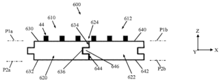
본 개시의 원리들에 따른 타일링된 디스플레이(600)의 다른 실시예의 부분들이 간략화된 형태로 도 10에 도시된다. 상기 타일링된 디스플레이(600)는 위의 설명들과 유사할 수 있으며, 복수의 타일들, 예컨대 제1 및 제2 타일들(610, 612)을 포함한다. 상기 타일들(610, 612) 각각은 위의 설명들과 일관된 기판, 예컨대 기판들(620, 622)을 각각 포함한다. 상기 타일들(610, 612)은 이전에 설명된 임의의 디스플레이 기술들을 복수의 픽셀들 또는 픽셀 요소들(44)을 수반하는 대응하는 기판들(620, 622)에 통합할 수 있다. 상기 픽셀들(44)은 상기 타일링된 디스플레이(600)의 최종 조립 시 전체적으로 상기 타일링된 디스플레이(600)의 배열로 배열되며, 상기 배열은 위에 설명된 바와 같이 균일한 픽셀 피치를 각각 가지는 복수의 행들 및 열들을 포함한다. 상기 행들 내의 픽셀 피치는 상기 열들 내의 픽셀 피치와 동일하거나 상이할 수 있다. 상기 이웃하는 제1 및 제2 타일들(610, 612)은 그들 사이에 형성된 경계(624)에 걸친 상기 소정의 선형 방향으로의 균일한 픽셀 피치를 유지하는 상보적인 형상 피쳐들 및 픽셀 배열들을 가진다.Portions of another embodiment of a
상기 제1 타일 기판(620)은 대향하는 제1 및 제2 주면들(630, 632) 및 상기 주면들(630, 632) 사이에 Z 또는 깊이 방향으로 연장되는 제1 엣지(634)를 정의한다. 상기 대향하는 주면들(630, 632) 각각은 주평면(P1a, P2a)을 정의한다. 상기 제1 엣지(634)의 엣지 프로파일의 적어도 일부는 상기 주평면들(P1a, P2a)에 수직하지 않다. 예를 들어, 상기 제1 엣지(634)의 프로파일은 슬롯(636)을 형성할 수 있다. 상기 제2 타일 기판(622)은 또한 대향하는 제1 및 제2 주면들(640, 642) 및 상기 주면들(640, 642) 사이에 Z 또는 깊이 방향으로 연장되는 제1 엣지(644)를 정의한다. 대향하는 주면들(640, 642) 각각은 주평면(P1b, P2b)을 정의한다. 상기 제1 엣지(644)의 엣지 프로파일의 적어도 일부는 상기 주평면들(P1b, P2b)에 수직하지 않다. 특히, 상기 제2 타일 제1 엣지(644)는 립(rib)(646)을 형성할 수 있다. 상기 슬롯(646)과 상기 립(646)은 상보적인 구성을 가질 수 있다.The
상기 타일링된 디스플레이(600)의 최종 조립시, 상기 제1 타일 제1 엣지(634)는 상기 제2 타일 제1 엣지(644)와 대면하여 상기 경계(624)를 정의하고, 상기 립(646)은 상기 슬롯(636) 내에 끼워진다. 상기 상보적인 엣지 프로파일들은 인접한 타일들(610, 612)의 상보적인 맞춤 및 상기 픽셀들(44)의 수직 정렬을 가능하게한다. 상기 엣지들(634, 644)은 서로 물리적으로 접촉하거나 하지 않을 수 있다. 또한, 이러한 상보적인 맞춤과 상기 대응하는 기판 제1 엣지(633, 644)에 대하여 상기 픽셀들(44)의 배열은 결합하여 위의 설명들과 상응하게 상기 소정의 선형 방향으로 상기 경계(624)에 걸쳐 균일한 픽셀 피치를 유지한다.Upon final assembly of the
도 6 내지 도 10을 참조하여 위에 설명된 상기 상보적인 기판 엣지 프로파일들은 몇 개의, 본 개시에 의해 구상되는 선택적인 엣지 프로파일들의 비제한적 예들이다. 상기 기판 엣지 프로파일들은 사각형이거나, 둥글거나, 각지거나, 비선형 프로파일을 가질 수 있다. 또한, 특정 기판의 모든 엣지들은 동일한 프로파일을 가지거나 가지지 않을 수 있다. 일부 실시예들에서, 하나 이상의 상기 엣지 프로파일들은 물리적 접촉 및/또는 광학적 효과들을 관리하기 위한 추가적인 코팅들을 가질 수 있다. 상기 엣지 프로파일(들)은 다양한 방식들로 특정 기판으로 구현될 수 있다. 예를 들어, 본 개시의 엣지 프로파일들을 생성하는 일부 방법들은 기계적 스크라이브, 레이저 절단, 식각, 열 성형, 그라인딩 등을 포함한다. 또한, 다수의 공정들이 원하는 엣지 프로파일을 생성하는데 사용될 수 있다. 예를 들어, 상기 기판은 처음에는 기계적으로 스크라이브된 후, 식각될 수 있다. 위에 지적된 바와 같이, 상기 타일링된 디스플레이의 이웃한 타일들의 기판들에 의해 수반되는 상기 픽셀들(예를 들어, 발광 요소)은 둘레를 따라 대응하는 기판 엣지들로부터 상이한 거리들에 위치될 수 있다. 일부 실시예들에서, 예를 들어, 이러한 구성은 사용된 엣지 프로파일 형성 공정(들)에 따라 유익할 수 있다. 예를 들어, 두 기계적으로 스크라이브된 엣지들 및 두 그라인딩된 엣지들을 가지는 하나의 타일 기판은 실제 기판 엣지로부터 상이한 거리들에 위치하는 픽셀들(예를 들어, 마이크로-LED들)을 가질 수 있다. 이웃한 타일들이 조립되었을 때, 그러나, 타일간 픽셀 피치는 유지된다.The complementary substrate edge profiles described above with reference to FIGS. 6-10 are non-limiting examples of several optional edge profiles envisioned by the present disclosure. The substrate edge profiles may be rectangular, rounded, angular, or have a non-linear profile. Also, all edges of a particular substrate may or may not have the same profile. In some embodiments, one or more of the edge profiles may have additional coatings for managing physical contact and / or optical effects. The edge profile (s) can be implemented with a particular substrate in a variety of ways. For example, some methods of generating edge profiles of the present disclosure include mechanical scribe, laser cutting, etching, thermoforming, grinding, and the like. In addition, multiple processes can be used to create the desired edge profile. For example, the substrate may be initially mechanically scribed and then etched. As noted above, the pixels (eg, light emitting element) carried by the substrates of neighboring tiles of the tiled display may be located at different distances from corresponding substrate edges along the perimeter. . In some embodiments, for example, such a configuration may be beneficial depending on the edge profile forming process (es) used. For example, one tile substrate with two mechanically scribed edges and two ground edges may have pixels (eg, micro-LEDs) located at different distances from the actual substrate edge. When neighboring tiles are assembled, however, the inter-tile pixel pitch is maintained.
기판 절단/형성 공정들Substrate Cutting / Forming Processes
위에 지적된 바와 같이, 선택적인 기판 형상들 및/또는 기판 엣지 프로파일들은 다양한 기술들을 사용하여 특정 기판에 구현될 수 있다. 일부 실시예들에서, 하나 또는 양 피쳐들은 비회절 빔 절단을 통해 생성될 수 있다. 비회절 빔 절단 기술을 사용하여, 본 개시의 타일들에 유용한 유리 기판들은 위에 설명된 정밀한 타일 형상 및/또는 프로파일 및 치수들을 형성하도록 레이저-절단되거나 레이저 절단되고 화학적으로 식각될 수 있다. 비회절 빔 절단은 예를 들어 "시트와 같은 기판들의 레이저-기반 가공 방법 및 장치"라는 제목을 가지는 미국 출원 공개 제2014/0199519호에 설명되며, 그 교시 전체는 참조에 의해 본 명세서에 결합된다. 이러한 및 다른 공정들을 사용하면, 대형 기판 시트들(500mm보다 큰 치수)에 걸쳐 20μm 미만, 또는 더 작은 시트들(100mm 정도의 치수)에 걸쳐 10μm 미만의 치수 정확성으로 타일 기판들을 절단하는 것이 가능하다. 이러한 정확성은 이웃하는 타일들 사이의 위치 오차를 200μm 이하 정도일 수 있는 픽셀 피치의 50% 미만으로 유지하기 위해 중요할 수 있다. 이러한 선택적인 레이저 공정과 유리 기판들을 사용하면, 유리 절단 엣지들은 일반적으로 상기 기판의 전체 두께에 연장되는 얇은 수직 줄무늬들(striations)을 가질 수 있으며, 상기 줄무늬들 사이의 피치는 2-25μm 범위이다. 이러한 동일한 레이저 절단 공정들, 또는 식각 공정이 더해진 레이저 절단은 또한 더 복잡한 엣지 프로파일 피쳐들, 예컨대 도 9 및 10에 도시된 것들 등을 제조하는데 사용될 수 있다.As noted above, optional substrate shapes and / or substrate edge profiles may be implemented on a particular substrate using various techniques. In some embodiments, one or both features may be created through non-diffraction beam cutting. Using a non-diffraction beam cutting technique, glass substrates useful for the tiles of the present disclosure can be laser-cut or laser cut and chemically etched to form the precise tile shape and / or profiles and dimensions described above. Non-diffraction beam cutting is described, for example, in US Application Publication 2014/0199519 entitled "Method and Apparatus for Laser-Based Processing of Substrates, such as Sheets," the teachings of which are hereby incorporated by reference in their entirety. . Using these and other processes, it is possible to cut tile substrates with dimensional accuracy of less than 20 μm over large substrate sheets (dimensions larger than 500 mm), or less than 10 μm over smaller sheets (dimensions on the order of 100 mm). . This accuracy may be important to maintain the positional error between neighboring tiles to less than 50% of the pixel pitch, which may be on the order of 200 μm or less. Using this optional laser process and glass substrates, the glass cut edges can generally have thin vertical stripes extending over the entire thickness of the substrate, with the pitch between the stripes being in the range of 2-25 μm. . These same laser cutting processes, or laser cutting plus an etching process, can also be used to produce more complex edge profile features, such as those shown in FIGS. 9 and 10, and the like.
다른 실시예들에서, 레이저 구멍 뚫기 및 화학적 식각의 관련된 공정이 본 개시의 타일 기판에 선택적인, 원하는 피쳐들을 생성하는데 사용될 수 있다. 예를 들어, 위에 언급된 바와 같이, 일부 디스플레이 기술들에서, 하나 이상의 구멍들이 상기 타일 기판의 두께를 통해 형성되는 것이 바람직할 수 있다(예를 들어, 기판을 통한 금속 배선 및 전기 신호 전도를 가능하게 하는 관통-유리 비아들). 대안적으로 또는 추가적으로, 부분 병진 배치 또는 회전 배향을 위한 정렬 구멍들을 구현하는 것이 바람직할 수 있다. 식각된 부분들의 경우, 레이저 형성 공정의 특징이 여전히 분명할 수 있으나, 통상의 기술자에게 명백한 바와 같이 식각 공정에 의해 변경될 수 있다.In other embodiments, a related process of laser drilling and chemical etching can be used to create the desired features that are selective to the tile substrate of the present disclosure. For example, as mentioned above, in some display technologies, it may be desirable for one or more holes to be formed through the thickness of the tile substrate (eg, enabling metal wiring and electrical signal conduction through the substrate). Through-glass vias). Alternatively or additionally, it may be desirable to implement alignment holes for partial translational placement or rotational orientation. In the case of etched portions, the characteristics of the laser forming process may still be apparent, but may be altered by the etching process as will be apparent to those skilled in the art.
조립 방법들Assembly Methods
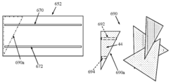
복수의 타일들로부터 타일링된 디스플레이를 조립하기 위해 다양한 방법들이 사용될 수 있다. 본 개시의 일부 실시예들에서, 예를 들어, 도 6에 의해 도시되는 바와 같이, 상기 타일들은 이웃한 타일들 사이의 물리적 분리를 생성하는 방식으로 조립될 수 있다. 폴리머 또는 다른 물리적 스페이서가 선택적으로 이러한 물리적 분리 내에 배치될 수 있다. 상기 타일 기판들 사이의 갭 내의 재료는 또한 대응하는 경계를 광학적으로 보이게 만들 수 있는 광을 최소화하는 선택적 기능을 수행할 수 있다. 광학적 효과들은 굴절률 정합 재료 또는 블랙 매트릭스 재료를 포함할 수 있다. 연질 재료, 예컨대 상기 타일 기판들 사이의 상기 갭 내의 폴리머는 또한 쿠션으로 기능하여 타일들이 서로에 접촉하도록 배치되었을 때 칩핑(hipping) 또는 다른 신뢰성을 손상시키는 결함들을 방지하도록 구성될 수 있다. 타일들의 엣지들 주위의 이러한 재료는 개별적인 타일들에 미리 적용될 수 있거나, 멀티-타일 디스플레이로의 조립 후에 적용될 수 있다. 상기 기판들 사이의 상기 재료는 또한 접착제일 수 있거나 접착제를 포함할 수 있다.Various methods may be used to assemble a tiled display from a plurality of tiles. In some embodiments of the present disclosure, for example, as shown by FIG. 6, the tiles can be assembled in a manner that creates a physical separation between neighboring tiles. Polymers or other physical spacers may optionally be disposed within this physical separation. The material in the gaps between the tile substrates can also perform an optional function of minimizing light that can make the corresponding boundary optically visible. Optical effects may include refractive index matching material or black matrix material. A soft material, such as a polymer in the gap between the tile substrates, can also be configured to function as a cushion to prevent defects that compromise chipping or other reliability when the tiles are placed in contact with each other. This material around the edges of the tiles can be applied in advance to the individual tiles or can be applied after assembly into the multi-tile display. The material between the substrates may also be an adhesive or may include an adhesive.
상기 타일들이 서로로부터 물리적으로 이격되는지와 무관하게, 본 개시의 일부 방법들은 상기 타일링된 디스플레이의 배면 상에 중첩되는 회로 기판 또는 기계적 마운팅이 있도록 타일들을 배열하는 단계를 포함한다. 배면 상의 이러한 중첩되는 회로 기판들 또는 기계적 마운팅들은 상기 타일링된 디스플레이를 구성하는 모든 조립된 타일들 아래에서 완전히 연장될 필요는 없으나, 적어도 두 이웃한 타일들의 부분들에 걸쳐 연장되어야 한다. 또한, 상기 타일들의 기계적 정렬은 다양한 방식들로, 예컨대 정렬 핀들 및 관통 구멍들에 의해 달성될 수 있다. 관련된 실시예들에서, 동적(kinematic) 마운팅 또는 결합이 제공될 수 있다. 예를 들어, 도 11은 본 개시의 일부 실시예들에 따른 타일링된 디스플레이의 조립체의 일부로서 기준 시트(652)에의 기판(650)의 동적 마운팅을 간략화된 형태로 도시한다. 상기 기판(650)은 위에 설명된 임의의 구성들을 가질 수 있는(예를 들어, 상기 기판(650)은 복수의 픽셀들(미도시)을 수반한다) 타일(654)의 일부로서 제공된다. 상기 기판(650)은 일반적으로 이전에 설명된 임의의 형태를 취할 수 있다; 도 11의 실시예에서, 하나 이상의 정렬 피쳐들, 예컨대 제1 및 제2 정렬 홈들(660, 662)이 상기 기판(650)의 주면(656)에 형성된다. 상기 기준 시트(652)는 결과적인 타일링된 디스플레이의 예상되는 치수들에 따른 크기 및 형상일 가질 수 있다(즉, 상기 타일링된 디스플레이를 형성할 때 조립되는 복수의 타일들이 상기 기준 시트(652) 상에 모두 매치된다). 상기 기준 시트(652)는 상기 조립된 타일링된 디스플레이 전체에 걸쳐 연장될 수 있거나 상기 타일링된 디스플레이를 구성하는 모든 조립된 타일들 아래에서 완전히 연장되지 않을 수 있다 (그러나 적어도 두 이웃하는 타일들의 부분들에 걸쳐 적어도 연장된다). 본 개시의 일부 방법들에서, 상기 기준 시트(652)는 상기 기판(650)의 상기 정렬 피쳐들과 대응하는 하나 이상의 기준 피쳐들, 예컨대 제1 및 제2 기준 홈들(672, 674)을 포함하거나 제공하는 기준 표면(670)을 정의한다. 상기 정렬 홈들(660, 662) 및 상기 기준 홈들(672, 674)은 아래에서 명백해지는 이유들로 인하여 실질적으로 동일한 형상 및 크기일 수 있으며, 각각은 핀(680, 682)의 일부를 각각 수용하도록 구성된다.Regardless of whether the tiles are physically spaced from each other, some methods of the present disclosure include arranging the tiles such that there is a circuit board or mechanical mounting that overlaps on the back of the tiled display. These overlapping circuit boards or mechanical mountings on the back need not extend completely below all of the assembled tiles that make up the tiled display, but must extend over at least two portions of two neighboring tiles. In addition, the mechanical alignment of the tiles can be achieved in various ways, such as by alignment pins and through holes. In related embodiments, kinematic mounting or coupling may be provided. For example, FIG. 11 illustrates in simplified form the dynamic mounting of the
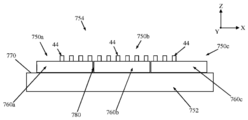
도 11의 구성에서, 타일링된 디스플레이의 제조는 상기 기준 시트(652)에 복수의 상기 타일들(654)을 조립하는 단계를 포함할 수 있으며, 여기서 상기 기준 시트(652)에 대한(및 서로에 대한) 각각의 상기 타일들(654)의 배치는 상기 핀들(680, 682)과의 계면에 의해 지시된다. 예를 들어, 상기 기준 시트(652) 상에 각각의 타일(654)을 배치하기 전에, 핀이 상기 기준 홈들 내로 로딩된다(예를 들어, 상기 핀들(680, 682)은 각각 상기 기준 홈들(672, 674) 내로 로딩된다). 상기 타일(654)은 이후 상기 핀들(680, 682)이 각각 상기 정렬 홈들(660, 662) 내에 수용되도록 상기 기준 시트(652) 상에 공간적으로 배열되어 놓인다. 상기 타일링된 디스플레이를 완성하기 위해 나머지 타일들에 대하여 이러한 동일한 공정이 반복된다. 이를 유념하면서, 기준/정렬 피쳐들 및 핀들은 서로에 대한 깊이(Z) 방향으로의 및 상기 디스플레이 평면(도 1의 X-Y 평면) 내의 타일들의 정렬 또는 레지스트레이션 중 하나 또는 둘 모두를 제공하도록 구성될 수 있다. 깊이 방향으로의 정렬은 각각의 상기 정렬 홈들(660, 662) 및 각각의 상기 기준 홈들(672, 674)의 형상을 각각의 상기 핀들(680, 682)의 직경과 상관시킴으로써 용이하게 될 수 있다. 상기 기준 홈들(672, 674)은 상기 기준 시트(652) 내에 정밀하게 형성되며, 따라서 상기 대응하는 핀(680, 682)은 상기 기준 표면(670)을 넘어 소정의 거리로 돌출된다. 상기 정렬 홈들(660, 662)은 대응하는 핀들(680, 682)과 정렬되어 그 상에 놓였을 때 상기 기판(650)이 상기 기준 시트(652) 위로(깊이 또는 Z 방향으로) 소정의 거리에 지지되며 유지되도록 상기 기판(650) 내에 정밀하게 형성된다. 나머지 타일들은 유사하게 상기 기준 시트(652)로부터 이러한 동의한 소정의 거리에 지지되며 유지된다. 따라서, 상기 타일링된 디스플레이의 타일들은 상기 깊이 방향으로 전체적으로 정렬된다.In the configuration of FIG. 11, fabrication of a tiled display may include assembling a plurality of the
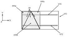
상기 타일링된 디스플레이의 타일들의 상기 디스플레이 평면(도 1의 X-Y 평면) 내의 정렬 또는 레지스트레이션은 상기 둘레 형상에 대해 상기 기판에 의해 수반되는 픽셀 행렬의 예상 배열에 대해 소정의 공간적 위치들(X-Y 평면 내의)에서 각각의 타일 기판들(650) 내에 정렬 홈들(660, 662)을 형성함으로써 용이해질 수 있다. 상기 기준 홈들(예를 들어, 기준 홈들(672, 674))은 상기 타일링된 디스플레이를 전체적으로 형성하는 각각의 타일들의 둘레 형상들 및 원하는 타일간 레지스트레이션과 대응하는 소정의 공간적 위치들에 기준 시트(652) 내에 형성된다. 이와 관련하여, 타일링된 디스플레이의 이웃한 타일들은 예상된 둘레 형상 및 이러한 둘레 형상 대하여 예상된 픽셀 행량 배열을 각각 가질 것이다. 이러한 이해에 기초하여, 기준 홈들은 형성되는 타일링된 디스플레이의 모든 타일에 대하여 제공하는 패턴으로 배열되며, 각각의 타일들의 상기 정렬 홈들은 상기 패턴에 따라 대응하는 타일에 따른 위치들에 형성된다. 비제한적 예로서, 도 12a는 상기 제1 및 제2 기준 홈들(672, 674)을 포함하는 기준 시트(652)의 간략화된 표현이다 (임의의 다른, 더 많거나 더 적은, 수의 기준 홈들도 동일하게 허용된다는 것이 이해될 것이다). 핀(미도시)은 위에 설명된 바와 같이 각각의 상기 기준 홈들(672, 674)과 함께 위치된다. 복수의 타일들(690)(일반적으로 참조됨)은 또한 조립을 위하여 상기 기준 시트(652) 상에 제공된다. 각각의 상기 타일들(690)의 기판은 상기 기준 시트(652)의 대응하는 상기 기준 홈들(672, 674)과 정렬되거나 짝지어졌을 때 소정의 위치에 대응하는 픽셀 행렬을 위치시키도록 배열된 정렬 홈들을 형성한다. 예를 들어, 제1 및 제2 정렬 홈들(692, 694)이 상기 제1 타일(690a)에 대하여 도시된다. 상기 정렬 홈들(692, 694)은 각각의 기준 홈들(672, 674)과 대응하도록 위치되며 배열되어, 상기 기준 시트(652) 상에 놓여졌을 때, 상기 제1 타일(690a)은 상기 기준 시트(652)에 대하여 알려진 방향으로 배열될 것이다(즉, 상기 기준 홈들(672, 674)과 상기 정렬 홈들(692, 694)의 정렬에 의해 지시된 상기 기준 시트(652)에 대한 상기 제1 타일(690a)의 알려진 방향이 도 12a에 팬텀(phantom)으로 도시된다). 이러한 알려진 방향에 기초하여, 상기 제1 타일(690a)의 상기 픽셀들(44)(일반적으로 참조됨)은 상기 픽셀들(44)이 상기 기준 시트(652) 상에 상기 제1 타일(690a)의 조립 시 상기 기준 시트(652)에 대하여 소정의 원하는 방식으로 공간적으로 배열되도록 상기 정렬 홈들(692, 694)(또는 그 반대) 및 상기 제1 타일(690a)의 둘레 형상(또는 그 반대)에 대하여 배열되며 위치된다.Alignment or registration in the display plane (XY plane of FIG. 1) of the tiles of the tiled display may be at predetermined spatial locations (in XY plane) relative to the expected arrangement of the pixel matrix carried by the substrate relative to the perimeter shape. Can be facilitated by forming the
도 12b는 상기 제1 타일(690a) 및 제2 및 제3 타일들(690b, 690c)이 상기 기준 시트(652) 상에 조립된 부분적으로 조립된 상태를 도시한다. 위의 설명들과 상응하여, 각각의 타일들(690a 내지 690c)의 기판의 정렬 홈들(숨겨짐)은 대응하는 기준 홈들(672, 674)과 짝지어지거나 정렬된다. 이러한 조정된 배열의 결과로서, 상기 제1-제3 타일들(690a-690c)의 상기 픽셀들(44)(일반적으로 참조됨) 및 엣지들은 상기 디스플레이(X-Y) 평면 내에 레지스터되고 정렬된다. 나머지 타일들(690d-690f)은 유사하게 상기 기준 시트(652) 상에 조립되어 도 12c에 도시된 바와 같이 완성된 타일링된 디스플레이(696)를 도출한다.12B illustrates a partially assembled state in which the
도 11 내지 도 12c에 의해 시사된 조립 방법들에서, 상기 기준 시트(652)는 임시적인 사용을 위하여 구성될 수 있다; 상기 기준 시트(652) 상에 조립된 후, 상기 타일들은 서로 접착 또는 고정될 수 있으며, 이후 상기 기준 시트(652)로부터 제거될 수 있다. 이러한 및 유사한 기술들에서, 상기 기준 시트(652)는 타일링된 디스플레이 동작에 대한 고려 없이 다양한 형태들을 취할 수 있으며, 다양한 재료들로 형성될 수 있다. 다른 실시예들에서, 상기 기준 시트(652)는 최종적인 타일링된 디스플레이의 영구적인 부분으로서 기능하도록 구성될 수 있으며, 따라서 알맞은 기계적, 전기적 및/또는 광학적 성질들을 가질 수 있다(예를 들어, 상기 기준 시트(652)는 상기 타일링된 디스플레이의 커버 시트 또는 플레이트로서 기능할 수 있으며, 강화된 유리일 수 있다). 상기 타일링된 디스플레이가 배면 광인 일부 실시예들에서, 상기 기준 시트(652)는 적어도 두 이웃한 배면 광 타일들의 부분들에 걸쳐 연장되는 관련된 액정 셀일 수 있다. 상기 기준 시트(652)는 상기 타일링된 디스플레이 전체에 걸쳐 연장되는 일체형 시트일 수 있다. 대안적으로, 상기 디스플레이 타일들을 조립하기 위해 사용되는 복수의 기준 시트들(652)이 있을 수 있다. 관련된 실시예들에서, 상기 기준 시트들(652) 그 자체가 타일링될 수 있다.In the assembly methods suggested by FIGS. 11-12C, the
본 개시의 상기 선택적인 동적 마운팅 기술들 및 방법들은 다른 형태를 취할 수 있다. 예를 들어, 도 13은 본 개시의 일부 방법들에 따른 타일링된 디스플레이를 형성 시, 기판 시트(702)에의 기판(700)의 동적 마운팅을 간략화된 형태로 도시한다(예를 들어, 상기 기판(700)은 복수의 픽셀들(미도시)을 수반한다). 상기 기판(700)은 위에 설명된 임의의 구성들을 가질 수 있는 타일(704)의 일부로서 제공된다(예를 들어, 상기 기판(700)은 복수의 픽셀들(미도시)을 수반한다). 상기 기판(700)은 일반적으로 이전에 설명된 임의의 형태들을 취할 수 있다; 도 13의 실시예에서, 하나 이상의 정렬 피쳐들, 예컨대 제1 및 제2 범프들(710, 712)이 상기 기판(700)의 주면(706)에 형성된다(임의의 다른, 더 크거나 더 작은, 수의 범프들이 동등하게 허용된다). 상기 기준 시트(702)는 결과적인 타일링된 디스플레이의 예상 치수에 따른 크기 및 형상을 가질 수 있다(즉, 타일링된 디스플레이들을 생성할 시 조립되는 상기 복수의 타일들은 상기 기준 시트(702) 상에 모두 놓인다). 본 개시의 일부 방법들에서, 상기 기준 시트(702)는 상기 기판(700)의 정렬 피쳐들과 대응하는 하나 이상의 기준 피쳐들, 예컨대 제1 및 제2 홈들(722, 724)을 포함하거나 제공하는 기준 표면(720)을 정의한다. 상기 범프들(710, 712)은 대응하는 상기 홈들(722, 724) 내에 수용되고 지지되도록 구성된다. 일부 실시예들에서, 상기 기준 표면(720)은 상기 범프(710, 712)를 상기 대응하는 홈(722, 724)과 완전히 맞물리도록 안내하는 기능을 하는 각각의 상기 홈들(722, 724)을 둘러싸는 융기된 릿지(ridge) 또는 유사한 구조를 더 포함할 수 있다. 도 11-12C와 관련한 위의 설명들과 유사하게, 둘 이상의 타일들(예컨대 타일(704))은 상기 홈들(예컨대, 홈들(722, 724))의 패턴 및 상기 범프들(예컨대 범프들(710, 712))과 상기 홈들 사이의 계면에 의해 지시되는 소정의 위치들에 상기 기준 시트(702) 상에 조립되며, 깊이(Z) 방향 및 디스플레이 평면(도 1의 X-Y 평면) 내의 타일간 정렬 또는 레지스트레이션 중 하나 또는 둘 모두를 야기한다.The optional dynamic mounting techniques and methods of the present disclosure may take other forms. For example, FIG. 13 illustrates in simplified form the dynamic mounting of a
도 11 내지 도 13의 실시예들에서, 타일간 레지스트레이션은 이웃하는 타일들의 엣지들 사이의 직접적인 정렬 접촉에 의존하지 않고 달성될 수 있다. 이러한 동일한 관점에서, 본 개시의 원리들에 따른 다른 타일링된 디스플레이의 조립 방법들은 타일링된 디스플레이(754)의 형성 시 복수의 타일들, 예컨대 타일들(750a, 750b, 750c)이 기준 시트(752)에 장착되는 도 14의 간략화된 도시에 의해 반영된다. 각각의 타일들(750a, 750b, 750c)은 위에 설명된 임의의 형태들을 취할 수 있으며(예를 들어, 이전에 설명된 임의의 디스플레이 기술들을 포함할 수 있다), 실질적으로 곧은 엣지들 및 실질적으로 직사각형의 프로파일들 또는 임의의 다른 형상을 가지는 균일한 직사각형 타일들일 수 있다. 또한, 각각의 상기 타일들(750a, 750b, 750c)은 복수의 픽셀들(44)을 수반하는 기판(760a, 760b, 760c)을 각각 포함한다. 상기 기판들(760a-760c)은 또한 위에 설명된 임의의 구성들을 가질 수 있으며, 일부 실시예들에서 치수 안정성을 가지도록 예컨대 유리, 유리 세라믹 또는 세라믹으로 구성된다. 각각의 상기 타일들(750a-750c)은 또한 하나 이상의 정렬 피쳐들을 더 포함한다. 아래에서 보다 상세히 설명되는 바와 같이, 상기 정렬 피쳐(들)은 대응하는 타일(750a-750c)의 둘레 엣지 외로 제공된다 (즉, 도 14의 실시예들과 관련된 상기 타일 정렬 피쳐(들)은 상기 대응하는 기판(760a-760c)의 엣지 또는 상기 대응하는 타일(750a-750c)의 임의의 다른 둘레 엣지가 아니다). 상기 기준 시트(752)는 결과적인 타일링된 디스플레이(754)의 예상 치수들에 따른 크기 및 형상을 가질 수 있고, 기준 표면(770)을 제공한다. 상기 기준 표면(770)은 모든 조립된 타일들에 걸쳐 연장될 수 있거나, 적어도 두 이웃한 타일들의 적어도 부분들을 덮을 수 있다. 상기 기준 표면(770) 자체는 타일링될 수 있다. 일반적으로, 상기 타일링된 디스플레이(754)의 제조는 상기 기준 표면(770) 상으로 각각의 상기 타일들(750a-750c)을 개별적으로 배치하는 단계, 이웃하는 타일 방식으로 서로에 근접하게 상기 타일들(750a-750c)을 대략적으로 배열하기 위하여 상기 기준 표면(770)을 따라 상기 타일들(750)을 조작하는 단계, 및 상기 대응하는 정렬 피쳐들을 정렬시킴으로써 이웃하는 타일들의 픽셀들(44)을 레지스터하는 단계를 포함한다. 도 14의 조립 방법들은 상기 디스플레이 평면(도 1의 X-Y 평면) 내에서 바로 이웃하는 타일들(예를 들어, 이웃하는 제1 및 제2 타일들(750a, 750b), 및 이웃하는 제2 및 제3 타일들(750b, 750c)) 사이의 픽셀들(44)의 레지스트레이션 또는 정렬을 달성하게 한다; 이웃한 타일들 사이의 엣지간 접촉은 조립 및 픽셀 레지스트레이션에 의존하지 않는다. 타일들(750a-750c)의 엣지들에 기초한 레지스트레이션이 요구되지 않는다. 대신, 픽셀 레지스트레이션은 정밀하게 각각의 상기 기판들(760a-760c)의 상에 배치/생성된 피쳐들에 기초하며 엣지 위치 또는 형상 변동에 의존하지 않은다. 따라서, 상기 타일 엣지들의 직진성 또는 거칠기의 임의의 불가피한, 통계적 변동들은 원하는 픽셀 레지스트레이션에 영향을 미치지 않는다.In the embodiments of FIGS. 11-13, inter-tile registration can be accomplished without relying on direct alignment contact between the edges of neighboring tiles. In this same respect, other tiled display assembly methods in accordance with the principles of the present disclosure are characterized in that a plurality of tiles, such as
각각의 상기 타일들(750a-750c)에 제공되는 정렬 피쳐(들)은 다양한 형태들을 취할 수 있다. 예를 들어, 각각의 타일들(750a-750c)에 제공된 하나(또는 그 이상)의 픽셀들(44)은 정렬 피쳐들로 기능할 수 있다. 이와 관련하여, 상기 타일들(750a-750c)은 마이크로-LED 또는 LED 디스플레이 기술을 포함하는 경우(예를 들어, 도 14의 각각의 픽셀들(44)은 하나 이상의 마이크로-LED들 또는 LED들을 포함함), 특정 타일의 정렬 피쳐로 지정된 단일 또는 복수의 마이크로 LED들(또는 LED들)은 조립 공정 동안 밝혀질(전기적으로 또는 광학적으로 여기될) 수 있다. 이러한 및 관련된 실시예들에서, 이웃한, 제1 및 제2 타일들(750a, 750b)의 픽셀들(44)을 레지스터하는 단계는 각각의 타일들(750a, 750b)의 선택된 하나(또는 그 이상)의 마이크로-LED 픽셀들(44)을 밝히는 단계 및 이후 상기 밝혀진 마이크로-LED 픽셀들(44)을 광학적으로 정렬시키는 단계를 포함할 수 있다. 각각의 타일들(750a-750c)에 제공된 상기 정렬 피쳐(들)은 다른 형태들, 예컨대 TFT(제공된 경우) 또는 전자 인터커넥트 패터닝 내의 구조들, 패터닝된 레지스트레이션 마크들을 취할 수 있다. 상기 정렬 피쳐(들)은 아래에서 설명된 바와 같이 비젼(vision) 시스템 및 능동 정렬 방법들과의 조합으로의 사용을 위하여 생성될 수 있다. 대안적으로, 정렬 피쳐(들)은 위에서 설명된 바와 같이 상기 타일들의 정렬을 가능하게 하는 물리적 동적 구조들일 수 있다. 여하튼, 위에서 언급된 바와 같이, 도 14의 실시예들과 관련된 정렬 피쳐(들)은 상기 대응하는 타일(750a-750c)의 둘레 엣지와 다른 것이다.The alignment feature (s) provided on each of the
정렬 피쳐(들) 외에, 도 14의 실시예에 의해 시사되는 타일들(예를 들어, 타일들(750a-750c)은 위에서 설명된 임의의 구성들을 가질 수 있다. 상기 타일들은 직사각형, 육각형, 삼각형, 또는 서로에 대하여 조립되었을 때 결과적인 픽셀 배열 내에 공극들을 남기지 않는 임의의 다른 단위 형상들일 수 있다. 전체적으로 조립된 타일링된 디스플레이 내의 개별적인 타일들 전부는 동일한 형상 또는 치수를 가지거나 가지지 않을 수 있다. 일부 실시예들에서, 개별적인 타일들은 의도적으로 결과적인 타일링된 디스플레이(754)의 원하는 외곽 치수들보다 작은 크기를 가질 수 있다. 예를 들어, 각각의 상기 타일들(750a-750c) 및 특히 각각의 대응하는 기판들(760a-760c)은 이론적으로 동일한 길이(X 방향)를 가지도록 설계된다. 결합된 기판 길이들(X 방향)은 결과적인 타일링된 디스플레이(754)의 원하는 길이(X 방향)보다 작게 설계된다. 달리 말해, 상기 타일들(750a 내지 750c)은 최종 조립 시 이웃하는 타일들이 서로로부터 다소 이격되게 설계된다 (예를 들어, 도 14의 도면에서, 상기 제1 및 제2 타일들(750a, 750b)의 마주보는 엣지들은 경계(780)에서 서로로부터 이격된다). 이러한 선택적인 접근법에서, 이웃한 타일들에 걸친(즉, 상기 경계(780)에 걸친) 원하는 픽셀 레지스트레이션은 상기 타일 엣지들(예를 들어, 상기 기판들(750a-750c)의 엣지들)의 예상되는 직진도 및/또는 거칠기 성질들의 불가피한 변동들에 의해 부정적으로 영향을 받지 않는다. 다른 실시예들에서, 이웃하는 타일들은 서로 접촉할 수 있다.In addition to the alignment feature (s), the tiles suggested by the embodiment of FIG. 14 (eg,
상기 기준 시트(752)는 본 명세서에 설명된 조립 방법들(예를 들어, 상기 기준 표면(770)을 따라 상기 타일들(750a-750c)을 조작하는(예를 들어 미는) 단계)을 촉진하기에 적합한 다양한 형태들을 취할 수 있다. 예를 들어, 상기 기준 시트(752)는 연속적인 바디(예를 들어, 유리 시트)일 수 있거나, 비연속적인 프레임 구조일 수 있다. 상기 기준 시트(752)는 상기 기판들(760a-760c)의 두께(깊이 방향)와 동일한 두께를 가질 수 있거나, 더 얇을 수 있거나, 더 두꺼울 수 있다. 일부 실시예들에서, 상기 타일들(750a-750c)을 기준 표면(770)과 접촉한 상태에서 이동시키는 것(또는 이동시키지 않는 것)을 돕기 위하여 상기 기준 표면(770)은 원하는 방식으로 상대적인 마찰에 영향을 미치는 재료에 의해 형성되거나 그러한 재료로 코팅될 수 있다. 예를 들어, 상기 기준 표면(770)에 대한 타일들(750a-750c)의 미끄러짐(예를 들어, 상기 기판들(760a-760c)과의 저 마찰, 미끄러짐 계면)을 촉진하기 위해 자가-조립 단일 층(self-assembled monolayer, SAM)과 같은 저마찰 계수 코팅이 상기 기준 표면(770)에 적용될 수 있다. 대안적으로 또는 추가적으로, 하나 이상의 상기 타일 기판들(760a-760c)은 원하는 방식으로 상기 기준 표면(770)과의 마찰 계면에 영향을 미치는 코팅 또는 재료를 가질 수 있다. 일부 실시예들에서, 상기 기준 시트(752)는 상기 기준 표면(770)에 대하여 상기 개별적인 타일들(750a-750c)의 예상되는 배치에 대응하는 위치들에 배치된 하나 이상의 레지스트레이션 피쳐들(미도시)을 더 포함할 수 있다. 이러한 및 관련된 실시예들에서, 본 개시의 방법들은 선택적으로 각각의 레지스트레이션 피쳐들과 대응하는 타일(750a-750c)의 상기 정렬 피쳐를 정렬함으로써 타일-기준 표면간 표면 정렬을 수행하는 단계를 더 포함할 수 있다(예를 들어, 이웃한 타일들 사이의 대략적인 정렬은 상기 기준 시트(752)의 레지스트레이션 피쳐들과의 정렬을 통해 수행될 수 있으며, 이웃하는 타일들의 정렬 피쳐들의 정렬을 통한 미세한 정렬이 뒤따른다).The
위의 설명들에 의해 시사되는 타일링된 디스플레이 조립의 일부 방법들은 먼저 상기 기준 표면(770) 상에 개별적으로 타일들을 배치하는 단계 및 이후 대응하는 정렬 피쳐들을 통해 상기 타일들(및 특히 픽셀들)을 하나씩 정렬하는 단계를 포함할 수 있다. 예를 들어, 도 15a는 상기 제1 및 제2 타일들(750a, 750b)이 상기 기준 표면(770) 상으로 배치된 초기 조립 단계를 도시한다. 일부 실시예들에서, 상기 타일들(750a, 750b)의 휨 강성(flexural rigidity)(예를 들어, 대응하는 기판들(760a, 760b)(도 14)의 휨 강성)에 따라, 타일들(750a, 750b)은 굴림/굽힘, 수직, 수평 또는 결합된 이동으로 상기 기준 표면(770)으로 도입될 수 있다. 무관하게, 도 15b에서와 같이, 상기 제2 타일(750b)은 이후 상기 제1 및 제2 타일들(750a, 750b)이 서로 이웃하며 상기 제1 타일(750a)의 엣지가 상기 제2 타일(750b)의 엣지와 마주보며 그들 사이에 경계(780)를 대략적으로 형성하도록 상기 제1 타일(750a)에 대하여(및/또는 반대로) 조작된다(예를 들어, 상기 기준 표면(770)을 따라 미끄러진다). 위에서 언급된 바와 같이, 일부 실시예들에서, 상기 타일들(750a, 750b)의 대략적인 정렬은 상기 기준 시트(752)에 선택적으로 제공된 기준 피쳐들(미도시)을 참조하여 이루어질 수 있다. 상기 기준 표면(770) 상의 상기 정렬 피쳐(들)은 또한 최종적인 타일 정렬에 사용될 수 있다. 대안적으로, 일부 실시예들에서, 대략적인 정렬은 타일들(750a, 750b)의 엣지들 사이의 물리적 접촉에 의해 촉진될 수 있다. 이 조립 단계에서, 상기 제1 및 제2 타일들(750a, 750b)의 픽셀들(44)은 서로 레지스터되거나 되지 않을 수 있다. 또한, 상기 제1 및 제2 타일들(750a, 750b)의 정렬 피쳐들은 이후 상기 제1 타일(750a)의 픽셀들(44)을 상기 제2 타일(750b)의 픽셀들(44)과 레지스터하도록 정렬된다. 예를 들어 도 15c는 상기 제1 타일(750a)의 정렬 피쳐(790a) 및 상기 제2 타일(750b)의 정렬 피쳐(790b)를 도시한다; 이러한 비제한적 예의 상기 정렬 피쳐들(790a, 790b)은 상기 각각의 타일들(750a, 750b)에 제공된 픽셀들(44) 중 선택된 것들이다. 상기 정렬 피쳐들(790a, 790b)은 식별되고(예를 들어, 각각의 상기 정렬 피쳐들(790a, 790b)을 포함하는 팍샐(들)이 밝혀지고), 이후 정렬된다(예를 들어, 광학적으로 정렬된다). 이러한 정렬 단계 후에, 상기 제1 및 제2 타일들(750a, 750b)의 픽셀들(44)은 서로에 대하여 레지스터되며, 각각의 타일들(750a, 750b)에 형성된 균일한 픽셀 피치와 대응하는 경계(780)에 걸친 픽셀 피치를 포함한다. 상기 제3 타일(750c)(도 14)이 이후 유사한 방식으로 상기 기준 표면(770) 상에 배치되고, 상기 제2 타일(750b)에 대하여 레지스터된다. 다른 실시예들에서, 병렬 조립 공정에서, 다수의 개별적인 타일들은 상기 기준 기판(770) 상에 배치되고 이후 상기 다수의 타일들의 정렬을 수행하기 위해 기계적/기계 비젼 시스템이 사용된다. 전체적으로, 상기 타일들(750a-750c)의 레지스트레이션은 타일-타일 정렬 피쳐들 및/또는 타일-기준 시트 정렬 피쳐들의 사용에 의해 수행될 수 있다.Some methods of tiled display assembly, as suggested by the above descriptions, first arrange the tiles individually on the
도 14로 돌아가면, 정렬되고 레지스터된 후에, 상기 타일들(예를 들어, 타일들(750a-750c)은 서로에 대하여 고정되어 상기 타일링된 디스플레이(754)를 완성한다. 타일들(750a-750c)이 그들 사이의 물리적 분리를 생성하는 방식으로 조립된 경우, 상기 물리적 분리는 위에서 설명된 바와 같이 이후 기계적 접촉을 막는 폴리머 또는 다른 물리적 스페이서 요소를 가질 수 있다. 일부 실시예들에서, 상기 기준 시트(752)는 일시적 사용을 위하여 구성될 수 있다; 상기 기준 시트(752) 상에서 조립된 후, 상기 타일들(750a-750c)은 서로에 접착 또는 고정될 수 있으며, 이후 상기 기준 시트(752)로부터 제거될 수 있다. 이러한 및 유사한 기술들에서, 상기 기준 시트(752)는 디스플레이 동작에 대한 고려 없이 다양한 형태들을 취할 수 있으며, 다양한 재료들로 형성될 수 있다. 다른 실시예들에서, 상기 기준 시트(752)는 상기 타일링된 디스플레이(754)의 영구적인 부분으로서 기능하도록 구성될 수 있으며, 따라서 적합한 기계적, 전기적 및/또는 광학적 성질들을 가질 수 있다(예를 들어, 상기 기준 시트(752)는 상기 타일링된 디스플레이의 커버 시트 또는 플레이트로서 기능할 수 있으며, 강화된 유리일 수 있다). 상기 타일링된 디스플레이가 배면 광인 경우, 상기 기준 시트(752)는 적어도 두 이웃하는 배면 광 타일들의 부분들에 걸쳐 연장되는 관련된 액정 셀일 수 있다. 일부 실시예들에서, 굽은(평평하지 않은) 타일링된 디스플레이가 요구되는 경우, 상기 타일링된 디스플레이(754)는 상기 기준 시트(252)가 평평한 상태로 조립될 수 있다. 상기 타일링된 디스플레이(754)의 조립 후, 상기 기준 시트(752)는 평평하지 않은 디스플레이를 생성하도록 원하는 형상으로 냉간 굽힘될 수 있다. 대안적으로, 상기 기준 시트(752)는 처음에 타일들(750a-750c)이 조립되는 굽은 형상을 가질 수 있다. 최종적인 굽은 디스플레이는 0.1m 이하, 대안적으로 0.5m 이하, 대안적으로 1m 이하, 대안적으로 5m 이하, 및 일부 실시예들에서 10m 이하의 곡률 반경을 가질 수 있다. 상기 X-Y 평면 내에서의 타일들의 레지스트레이션 및 조립을 가능하는 것에 더하여, 상기 기준 표면(770)은 또한 Z 방향으로의 타일 레지스트레이션을 제공한다. 예를 들어, 상기 기준 표면(770)은, 일부 실시예들에서, 이웃한 타일들이 Z 방향으로 상기 기판 두께의 50% 이하, 대안적으로 40% 이하, 대안적으로 30% 이하, 대안적으로 20% 이하, 대안적으로 10% 이하, 대안적으로 5% 이하, 및 일부 실시예들에서 1% 이하로 오프셋되는 타일 배치를 가능하게 할 수 있다.Returning to FIG. 14, after being aligned and registered, the tiles (eg,
청구된 주제의 범위로부터 벗어나지 않고 다양한 수정들 및 변형들이 본 명세서에 설명된 실시에들에 이루어질 수 있다. 따라서 이러한 수정들 및 변경들이 첨부된 청구항들 및 그 균등물들의 범위 내에 속하는 한 본 명세서가 본 명세서에 설명된 다양한 실시예들의 수정들 및 변형들을 커버하도록 의도된다.Various modifications and variations can be made to the embodiments described herein without departing from the scope of the claimed subject matter. Thus, it is intended that this specification cover modifications and variations of the various embodiments described herein as long as such modifications and changes fall within the scope of the appended claims and their equivalents.
Claims (43)
균일한 픽셀 피치(pitch)로 배열된 픽셀들의 행렬을 수반하는 기판을 포함하는 제1 타일; 및
상기 균일한 픽셀 피치로 배열된 픽셀들의 행렬을 수반하는 기판을 포함하는 제2 타일을 포함하고,
상기 제1 타일의 상기 기판은 대향하는 제1 및 제2 주면들(main surfaces) 및 상기 대향하는 주면들 사이에서 상기 기판의 깊이 방향으로 연장되는 제1 엣지를 포함하고,
상기 제1 타일의 상기 픽셀들의 행렬은 상기 제1 타일의 상기 제1 엣지에 가장 근접하게 위치된 제1 픽셀을 포함하고,
상기 제2 타일의 상기 기판은 대향하는 주면들 및 상기 제2 타일의 상기 기판의 깊이 방향으로 연장되는 제1 엣지를 포함하고,
상기 제1 엣지들은 상보적인 형상을 가지고,
상기 타일링된 디스플레이의 최종 조립체는,
그들 사이에 제1 경계(seam)를 형성하도록 서로 마주보는 상기 제1 엣지들을 포함하고,
상기 제1 타일의 픽셀들은 상기 제2 타일의 픽셀들과 레지스터(register)되고, 소정의 선형 방향으로 상기 제1 경계에 걸쳐 상기 균일한 픽셀 피치가 유지되고,
상기 제1 픽셀은 상기 복수의 행들 중 제1 행 및 상기 복수의 열들 중 제1 열 내에 정렬되고,
상기 제2 타일의 픽셀들은 상기 제1 행 또는 상기 제1 열을 따라 상기 제1 타일의 픽셀들 사이에 개재되지 않고;
상기 상보적인 형상은,
상기 제1 경계의 적어도 일부가 상기 복수의 행들에 비스듬함, 및
상기 제1 타일의 상기 제1 엣지의 적어도 일부가 상기 대응하는 대향하는 주면들의 평면에 수직하지 않도록 상기 제1 타일의 상기 제1 엣지가 상기 깊이 방향으로 프로파일됨
으로 구성된 군으로부터 선택된 적어도 하나의 특징을 포함하는 타일링된 디스플레이.A tiled display having an array of pixels arranged in a plurality of rows and a plurality of columns, the tiled display comprising:
A first tile comprising a substrate carrying a matrix of pixels arranged at a uniform pixel pitch; And
A second tile comprising a substrate carrying a matrix of pixels arranged at said uniform pixel pitch,
The substrate of the first tile includes opposing first and second main surfaces and a first edge extending in a depth direction of the substrate between the opposing major surfaces,
The matrix of pixels of the first tile includes a first pixel located closest to the first edge of the first tile,
The substrate of the second tile includes opposing major surfaces and a first edge extending in a depth direction of the substrate of the second tile,
The first edges have a complementary shape,
The final assembly of the tiled display is
The first edges facing each other to form a first seam between them,
The pixels of the first tile are registered with the pixels of the second tile, the uniform pixel pitch is maintained across the first boundary in a predetermined linear direction,
The first pixel is aligned within a first row of the plurality of rows and a first column of the plurality of columns,
The pixels of the second tile are not interposed between the pixels of the first tile along the first row or the first column;
The complementary shape is,
At least a portion of the first boundary is oblique to the plurality of rows, and
The first edge of the first tile is profiled in the depth direction such that at least a portion of the first edge of the first tile is not perpendicular to the plane of the corresponding opposing major surfaces.
A tiled display comprising at least one feature selected from the group consisting of:
상기 제1 타일의 상기 기판은 상기 대응하는 주면들 사이에 연장되는 제2 엣지를 더 포함하고, 상기 제2 엣지는 상기 제1 타일의 상기 제1 엣지와 코너를 형성하고, 또한 상기 제1 타일의 상기 픽셀들의 매트리스는 상기 제2 엣지에 가장 근접하게 위치된 제2 픽셀을 더 포함하고, 상기 타일링된 디스플레이는,
상기 균일한 픽셀 피치로 배열된 픽셀들의 행렬을 수반하는 기판을 포함하는 제3 타일을 더 포함하고, 상기 제3 타일의 상기 기판은 대향하는 주면들 및 상기 대응하는 주면들 사이에 연장되는 제1 엣지를 포함하고,
상기 제1 타일의 상기 제2 엣지 및 상기 제3 타일의 상기 제1 엣지는 상보적인 형상을 가지고;
또한 상기 타일링된 디스플레이의 최종 조립체는,
그들 사이에 제2 경계를 형성하도록 서로 마주보는 상기 제1 타일의 상기 제2 엣지와 상기 제3 타일의 상기 제1 엣지, 및
상기 제3 타일의 픽셀들과 레지스터되고, 상기 소정의 선형 방향으로 상기 제2 경계에 걸쳐 상기 균일한 픽셀 피치가 유지되는 상기 제1 타일의 픽셀들을 포함하는 타일링된 디스플레이.According to claim 1,
The substrate of the first tile further comprises a second edge extending between the corresponding major surfaces, the second edge defining a corner with the first edge of the first tile, and further comprising the first tile The mattress of the pixels of further comprises a second pixel located closest to the second edge, wherein the tiled display comprises:
A third tile comprising a substrate carrying a matrix of pixels arranged at a uniform pixel pitch, wherein the substrate of the third tile extends between opposing major surfaces and corresponding major surfaces; Including edges,
The second edge of the first tile and the first edge of the third tile have a complementary shape;
In addition, the final assembly of the tiled display,
The second edge of the first tile and the first edge of the third tile facing each other to form a second boundary therebetween, and
And a pixel of the first tile that is registered with the pixels of the third tile and wherein the uniform pixel pitch is maintained across the second boundary in the predetermined linear direction.
상기 제1 타일의 상기 제2 엣지 및 상기 제3 타일의 상기 제1 엣지의 상기 상보적인 형상은,
상기 제2 경계의 적어도 일부가 상기 복수의 행들에 비스듬함; 및
상기 제1 타일의 상기 제2 엣지 및 상기 제3 타일의 상기 제1 엣지 각각의 적어도 일부가 상기 대응하는 대향하는 주면들의 평면에 수직하지 않도록 상기 제1 타일의 상기 제2 엣지 및 상기 제3 타일의 상기 제1 엣지가 각각 상기 깊이 방향으로 각각 프로파일됨
으로 구성된 군으로부터 선택된 적어도 하나의 특징을 포함하는 타일링된 디스플레이.The method of claim 2,
The complementary shape of the second edge of the first tile and the first edge of the third tile is
At least a portion of the second boundary is oblique to the plurality of rows; And
The second edge and the third tile of the first tile such that at least a portion of each of the second edge of the first tile and the first edge of the third tile is not perpendicular to the plane of the corresponding opposing major surfaces The first edges of are each profiled in the depth direction, respectively
A tiled display comprising at least one feature selected from the group consisting of:
상기 제2 타일의 상기 기판 및 상기 제3 타일의 상기 기판은 각각 제2 엣지를 더 포함하고, 상기 제1 타일 및 상기 제2 타일의 상기 제2 엣지들은 상보적인 형상을 가지고, 또한 상기 타일링된 디스플레이의 최종 조립체는,
그들 사이에 제3 경계를 형성하도록 서로 마주보는 상기 제2 타일의 상기 제2 엣지 및 상기 제3 타일의 상기 제2 엣지, 및
상기 제3 타일의 픽셀들과 레지스터되고, 상기 소정의 선형 방향으로 상기 제3 경계에 걸쳐 상기 균일한 픽셀 피치가 유지되는 상기 제2 타일의 픽셀들을 포함하는 타일링된 디스플레이.The method of claim 2,
The substrate of the second tile and the substrate of the third tile each further comprise a second edge, wherein the second edges of the first tile and the second tile have a complementary shape, and the tiled The final assembly of the display is
The second edge of the second tile and the second edge of the third tile facing each other to form a third boundary therebetween, and
And a pixel of the second tile that is registered with the pixels of the third tile and wherein the uniform pixel pitch is maintained across the third boundary in the predetermined linear direction.
상기 제2 타일의 상기 제2 엣지 및 상기 제3 타일의 상기 제2 엣지의 상기 상보적인 형상은,
상기 제3 경계의 적어도 일부가 상기 복수의 행들에 비스듬함; 및
각각의 상기 제2 타일의 상기 제2 엣지 및 상기 제3 타일의 상기 제2 엣지의 적어도 일부가 상기 대응하는 대향하는 주면들의 평면에 수직하지 않도록 상기 제2 타일의 상기 제2 엣지 및 상기 제3 타일의 상기 제2 엣지는 각각 상기 깊이 방향으로 프로파일됨
으로 구성된 군으로부터 선택된 적어도 하나의 특징을 포함하는 타일링된 디스플레이.The method of claim 4, wherein
The complementary shape of the second edge of the second tile and the second edge of the third tile is
At least a portion of the third boundary is oblique to the plurality of rows; And
The second edge and the third of the second tile such that at least some of the second edge of each second tile and the second edge of the third tile are not perpendicular to the plane of the corresponding opposing major surfaces The second edges of the tiles are each profiled in the depth direction
A tiled display comprising at least one feature selected from the group consisting of:
상기 제1 경계의 상기 일부는 비선형인 타일링된 디스플레이.According to claim 1,
And said portion of said first boundary is non-linear.
각각의 상기 제1 엣지들은 상기 대응하는 대향하는 주면들의 평면과 평행한 평면 내에서 비선형인 타일링된 디스플레이.According to claim 1,
Each of the first edges is a non-linear tiled display in a plane parallel to the plane of the corresponding opposing major surfaces.
상기 제1 경계는 선형인 타일링된 디스플레이.According to claim 1,
And the first boundary is linear.
상기 제1 경계의 전체는 상기 복수의 행들에 비스듬한 타일링된 디스플레이.The method of claim 8,
And wherein the entirety of the first boundary is oblique to the plurality of rows.
상기 제1 타일의 상기 제1 엣지는 상기 대응하는 제1 주면과 둔각을 형성하고, 상기 대응하는 제2 주면과 예각을 형성하는 타일링된 디스플레이.According to claim 1,
And the first edge of the first tile forms an obtuse angle with the corresponding first major surface and forms an acute angle with the corresponding second major surface.
상기 제1 타일의 상기 제1 엣지는 상기 대응하는 제1 주면과 둔각을 형성하고 상기 대응하는 제2 주면과 예각을 형성하는 타일링된 디스플레이.The method of claim 10,
And the first edge of the first tile forms an obtuse angle with the corresponding first major surface and forms an acute angle with the corresponding second major surface.
상기 제1 경계 내에 배치되며 상기 제2 타일의 상기 제1 엣지로부터 상기 제1 타일의 상기 제1 엣지를 이격시키는 프레임 요소를 더 포함하는 타일링된 디스플레이.The method of claim 11, wherein
And a frame element disposed within the first boundary and spaced apart from the first edge of the second tile by the first edge of the first tile.
상기 제2 타일의 상기 제1 엣지는 상기 대응하는 제1 주면과 예각을 형성하고, 상기 대응하는 제2 주면과 둔각을 형성하는 타일링된 디스플레이.The method of claim 10,
And the first edge of the second tile forms an acute angle with the corresponding first major surface and forms an obtuse angle with the corresponding second major surface.
상기 타일링된 디스플레이의 최종 조립체는 상기 제2 타일의 상기 제1 엣지와 평행한 상기 제1 타일의 상기 제1 엣지를 포함하는 타일링된 디스플레이.The method of claim 13,
And wherein the final assembly of the tiled display comprises the first edge of the first tile parallel to the first edge of the second tile.
상기 제1 타일의 상기 제1 엣지는 상기 대응하는 대향하는 주면들 사이에서 굴곡지고, 또한 상기 제2 타일의 상기 제1 엣지는 상기 대응하는 대향하는 주면들 사이에서 선형인 타일링된 디스플레이.According to claim 1,
And the first edge of the first tile is bent between the corresponding opposing major surfaces, and wherein the first edge of the second tile is linear between the corresponding opposing major surfaces.
상기 제1 엣지들은 상보적인 계단 형상들을 포함하는 타일링된 디스플레이.According to claim 1,
And the first edges comprise complementary staircase shapes.
상기 제1 타일의 상기 제1 엣지는 노치(notch)를 정의하고, 또한 상기 제2 타일의 상기 제1 엣지는 립(rib)을 정의하고, 또한 상기 타일링된 디스플레이의 상기 최종 조립체는 상기 노치와 정렬된 상기 립을 포함하는 타일링된 디스플레이.According to claim 1,
The first edge of the first tile defines a notch, the first edge of the second tile also defines a rib, and the final assembly of the tiled display is coupled with the notch. A tiled display comprising the aligned lips.
상기 제1 타일의 상기 제1 엣지와 상기 제2 타일의 상기 제1 엣지 사이에 배치된 스페이서를 더 포함하는 타일링된 디스플레이.According to claim 1,
And a spacer disposed between the first edge of the first tile and the first edge of the second tile.
상기 스페이서는 폴리머 재료를 포함하는 타일링된 디스플레이.The method of claim 18,
And the spacer comprises a polymeric material.
상기 제1 타일의 상기 기판의 상기 제1 주면은 베이스 플레이트에 마운팅하기 위한 홈 및 범프 중 적어도 하나를 포함하는 타일링된 디스플레이.According to claim 1,
And the first major surface of the substrate of the first tile comprises at least one of a groove and a bump for mounting to a base plate.
상기 균일한 픽셀 피치는 0.5mm 이하인 타일링된 디스플레이.According to claim 1,
And the uniform pixel pitch is 0.5 mm or less.
상기 균일한 픽셀 피치는 0.4mm 이하인 타일링된 디스플레이.The method of claim 21,
And the uniform pixel pitch is 0.4 mm or less.
상기 균일한 피치는 0.3mm 이하인 타일링된 디스플레이.The method of claim 22,
And the uniform pitch is 0.3 mm or less.
상기 제1 타일은 복수의 마이크로-LED들을 더 포함하는 타일링된 디스플레이.According to claim 1,
And the first tile further comprises a plurality of micro-LEDs.
상기 타일링된 디스플레이의 최종 조립체는 상기 소정의 선형 방향으로 상기 균일한 픽셀 피치의 50% 이하의 레지스트레이션 오차로 상기 제2 타일의 픽셀들과 레지스터된 상기 제1 타일의 픽셀들을 포함하는 타일링된 디스플레이.According to claim 1,
And wherein the final assembly of the tiled display comprises pixels of the second tile and pixels of the first tile registered with a registration error of 50% or less of the uniform pixel pitch in the predetermined linear direction.
상기 제1 타일의 상기 기판은 유리, 유리 세라믹, 및 세라믹으로 구성된 군으로부터 선택된 재료를 포함하는 타일링된 디스플레이.According to claim 1,
And the substrate of the first tile comprises a material selected from the group consisting of glass, glass ceramics, and ceramics.
상기 제1 타일의 상기 기판은 10 ppm/℃ 이하의 열 팽창 계수를 나타내는 타일링된 디스플레이.According to claim 1,
And the substrate of the first tile exhibits a coefficient of thermal expansion of 10 ppm / ° C. or less.
상기 제1 타일의 상기 기판은 50GPa 이상의 영률을 나타내는 타일링된 디스플레이.According to claim 1,
And wherein said substrate of said first tile exhibits a Young's modulus of at least 50 GPa.
상기 균일한 픽셀 피치로 배열된 픽셀들의 행렬 및 제2 타일의 임의의 둘레 엣지 외에 제공된 정렬 피쳐를 수반하는 기판을 포함하는 상기 제2 타일을 상기 기준 표면 상에 배치하는 단계;
제1 경계를 형성하도록 상기 제1 타일의 엣지가 상기 제2 타일의 엣지와 마주보도록 상기 기준 표면을 따라 상기 제1 타일에 대하여 적어도 상기 제2 타일을 조작하는 단계; 및
상기 제1 타일의 상기 픽셀들이 상기 제2 타일의 상기 픽셀들과 레지스터되도록 상기 제1 타일의 상기 정렬 피쳐를 상기 제2 타일의 상기 정렬 피쳐와 정렬하는 단계를 포함하고,
상기 정렬하는 단계 후에, 상기 소정의 선형 방향으로 상기 제1 경계에 걸쳐 상기 균일한 픽셀 피치가 유지되는 타일링된 디스플레이의 조립 방법.Disposing said first tile on a reference surface comprising a matrix of pixels arranged at a uniform pixel pitch and a substrate carrying a provided alignment feature apart from any circumferential edge of the first tile;
Placing said second tile on said reference surface comprising a matrix of pixels arranged at a uniform pixel pitch and a substrate carrying an alignment feature provided in addition to any peripheral edge of a second tile;
Manipulating at least the second tile with respect to the first tile along the reference surface such that an edge of the first tile faces an edge of the second tile to form a first boundary; And
Aligning the alignment feature of the first tile with the alignment feature of the second tile such that the pixels of the first tile register with the pixels of the second tile,
After said aligning, said uniform pixel pitch is maintained across said first boundary in said predetermined linear direction.
상기 제1 타일의 상기 정렬 피쳐를 상기 제2 타일의 상기 정렬 피쳐와 정렬하는 상기 단계는 상기 제1 타일의 상기 정렬 피쳐를 상기 제2 타일의 상기 정렬 피쳐와 광학적으로 정렬하는 단계를 포함하는 타일링된 디스플레이의 조립 방법.The method of claim 29,
Aligning the alignment feature of the first tile with the alignment feature of the second tile comprises tiling the alignment feature of the first tile with the alignment feature of the second tile Method of assembling the display.
상기 정렬 피쳐들은 마이크로-LED, 전자 인터커넥트 패터닝, 및 상기 제1 타일의 상기 기판 내로 패터닝된 레지스트레이션 마크(registration mark)로 구성된 군으로부터 선택되는 타일링된 디스플레이의 조립 방법.The method of claim 29,
And the alignment features are selected from the group consisting of micro-LEDs, electronic interconnect patterning, and a registration mark patterned into the substrate of the first tile.
상기 제1 타일 및 상기 제2 타일 각각의 상기 픽셀들은 적어도 하나의 마이크로-LED를 포함하고, 또한 상기 제1 타일 및 제2 타일 각각의 상기 정렬 피쳐는 상기 픽셀들의 대응하는 행렬 중 적어도 하나의 마이크로-LED를 포함하는 타일링된 디스플레이의 조립 방법.The method of claim 29,
The pixels of each of the first tile and the second tile comprise at least one micro-LED, and wherein the alignment feature of each of the first tile and the second tile is at least one micro of the corresponding matrix of pixels. A method of assembling a tiled display comprising an LED.
상기 정렬하는 단계 후에, 상기 방법은,
상기 제1 타일을 상기 제2 타일에 고정하는 단계; 및
상기 기준 표면으로부터 상기 제1 타일 및 상기 제2 타일을 제거하는 단계를 더 포함하는 타일링된 디스플레이의 조립 방법.The method of claim 29,
After the aligning, the method is
Fixing the first tile to the second tile; And
Removing the first tile and the second tile from the reference surface.
상기 정렬하는 단계 후에, 상기 방법은,
상기 기준 표면에 상기 제1 및 제2 타일들을 고정하는 단계;를 더 포함하고,
상기 기준 표면은 상기 타일링된 디스플레이의 구성인 타일링된 디스플레이의 조립 방법.The method of claim 29,
After the aligning, the method is
Fixing the first and second tiles to the reference surface;
And the reference surface is a configuration of the tiled display.
상기 기준 표면은 제1 기준 피쳐 및 상기 제2 기준 피쳐를 수반하는 시트를 포함하고, 또한 상기 조작하는 단계는,
상기 제1 기준 피쳐와 상기 제1 타일의 상기 정렬 피쳐를 정렬하는 단계; 및
상기 제2 기준 피쳐와 상기 제1 타일의 상기 정렬 피쳐를 정렬하는 단계를 포함하는 타일링된 디스플레이의 조립 방법.The method of claim 29,
The reference surface comprises a sheet carrying a first reference feature and the second reference feature, and wherein the manipulating comprises:
Aligning the alignment feature of the first tile with the first reference feature; And
Aligning the alignment feature of the first tile with the second reference feature.
상기 균일한 픽셀 피치는 0.5mm 이하인 타일링된 디스플레이의 조립 방법.The method of claim 29,
And said uniform pixel pitch is 0.5 mm or less.
상기 균일한 픽셀 피치는 0.4mm 이하인 타일링된 디스플레이의 조립 방법.The method of claim 36,
And said uniform pixel pitch is 0.4 mm or less.
상기 균일한 픽셀 피치는 0.3mm 이하인 타일링된 디스플레이의 조립 방법.The method of claim 37,
And said uniform pixel pitch is 0.3 mm or less.
상기 제1 타일의 상기 픽셀들은 복수의 마이크로-LED들을 포함하는 타일링된 디스플레이의 조립 방법.The method of claim 29,
And said pixels of said first tile comprise a plurality of micro-LEDs.
상기 타일링된 디스플레이의 최종 조립체는 상기 균일한 픽셀 피치의 50% 이하의 레지스트레이션 오차로 상기 제2 타일의 픽셀들과 레지스터된 상기 제1 타일의 픽셀들을 포함하는 타일링된 디스플레이의 조립 방법.The method of claim 29,
And wherein the final assembly of the tiled display comprises pixels of the second tile and pixels of the first tile registered with a registration error of 50% or less of the uniform pixel pitch.
상기 제1 타일의 상기 기판은 유리, 유리 세라믹, 및 세라믹으로 구성된 군으로부터 선택된 재료를 포함하는 타일링된 디스플레이의 조립 방법.The method of claim 29,
And said substrate of said first tile comprises a material selected from the group consisting of glass, glass ceramics, and ceramics.
상기 제1 타일의 상기 기판은 10 ppm/℃ 이하의 열 팽창 계수를 나타내는 타일링된 디스플레이의 조립 방법.The method of claim 29,
And said substrate of said first tile exhibits a coefficient of thermal expansion of 10 ppm / ° C. or less.
상기 제1 타일의 상기 기판은 50GPa 이상의 영률을 나타내는 타일링된 디스플레이의 조립 방법.The method of claim 29,
And said substrate of said first tile exhibits a Young's modulus of at least 50 GPa.
Applications Claiming Priority (3)
| Application Number | Priority Date | Filing Date | Title |
|---|---|---|---|
| US201762531110P | 2017-07-11 | 2017-07-11 | |
| US62/531,110 | 2017-07-11 | ||
| PCT/US2018/040845 WO2019014036A1 (en) | 2017-07-11 | 2018-07-05 | Tiled displays and methods of manufacturing the same |
Publications (2)
| Publication Number | Publication Date |
|---|---|
| KR20200024930A true KR20200024930A (en) | 2020-03-09 |
| KR102512945B1 KR102512945B1 (en) | 2023-03-22 |
Family
ID=65002203
Family Applications (1)
| Application Number | Title | Priority Date | Filing Date |
|---|---|---|---|
| KR1020207003909A KR102512945B1 (en) | 2017-07-11 | 2018-07-05 | Tiled displays and their manufacturing methods |
Country Status (6)
| Country | Link |
|---|---|
| US (1) | US11425826B2 (en) |
| JP (1) | JP7288427B2 (en) |
| KR (1) | KR102512945B1 (en) |
| CN (1) | CN110914751B (en) |
| TW (1) | TWI788380B (en) |
| WO (1) | WO2019014036A1 (en) |
Cited By (2)
| Publication number | Priority date | Publication date | Assignee | Title |
|---|---|---|---|---|
| US11049424B2 (en) * | 2018-02-06 | 2021-06-29 | Roe Visual Co., Ltd. | Splicing frame device and splicing method thereof |
| US11630632B2 (en) | 2021-02-25 | 2023-04-18 | Samsung Display Co., Ltd. | Pixel arrangement of display device and tiled display including the same |
Families Citing this family (26)
| Publication number | Priority date | Publication date | Assignee | Title |
|---|---|---|---|---|
| TWI781241B (en) * | 2017-11-08 | 2022-10-21 | 美商康寧公司 | Apparatus and methods for assembling a display area |
| US10950685B2 (en) * | 2018-03-29 | 2021-03-16 | Innolux Corporation | Tiled electronic device |
| KR102590433B1 (en) * | 2018-09-07 | 2023-10-18 | 삼성전자주식회사 | Display module, display apparatus including the same and method of manufacturing display module |
| US11275403B2 (en) * | 2019-03-08 | 2022-03-15 | Innolux Corporation | Tiled display device |
| US11908881B2 (en) | 2020-01-21 | 2024-02-20 | Seoul Viosys Co., Ltd. | LED display apparatus having micro LED module |
| US11776987B2 (en) * | 2020-01-21 | 2023-10-03 | Seoul Viosys Co., Ltd. | LED display apparatus having micro LED module |
| US11855052B2 (en) | 2020-01-22 | 2023-12-26 | Seoul Viosys Co., Ltd. | LED display apparatus having micro LED module |
| CN111276058B (en) * | 2020-02-11 | 2022-10-11 | 京东方科技集团股份有限公司 | Splicing display panel and splicing display device |
| CN111785182B (en) * | 2020-07-20 | 2022-07-12 | Tcl华星光电技术有限公司 | LED spliced panel |
| KR20220036444A (en) * | 2020-09-15 | 2022-03-23 | 삼성디스플레이 주식회사 | Tiling display device |
| CN112700753B (en) * | 2020-12-25 | 2024-03-15 | 视联动力信息技术股份有限公司 | Spliced screen display method and device, electronic equipment and storage medium |
| US20230092950A1 (en) * | 2021-01-05 | 2023-03-23 | Boe Technology Group Co., Ltd. | Display device |
| CN113146055B (en) * | 2021-02-24 | 2023-12-08 | 芜湖伦丰电子科技有限公司 | Laser engraving method of capacitive touch screen |
| CN113031331B (en) * | 2021-03-18 | 2022-08-05 | 苏州玉书屏新材料有限公司 | Low-cost giant liquid crystal display film and preparation process thereof |
| CN113219729A (en) * | 2021-05-10 | 2021-08-06 | 武汉华星光电技术有限公司 | Display panel and display device |
| CN113328030A (en) * | 2021-05-28 | 2021-08-31 | 北京京东方茶谷电子有限公司 | Light-emitting substrate, display panel and display device |
| CN113851054B (en) * | 2021-09-27 | 2023-07-25 | 武汉华星光电半导体显示技术有限公司 | Spliced screen |
| CN113903271B (en) * | 2021-09-28 | 2023-11-28 | 京东方科技集团股份有限公司 | Display module and spliced display device |
| CN114220359B (en) * | 2021-12-16 | 2023-03-28 | 深圳市华星光电半导体显示技术有限公司 | Back plate, display and display module |
| US11862051B2 (en) * | 2022-03-02 | 2024-01-02 | Tcl China Star Optoelectronics Technology Co., Ltd. | Display panel and light board |
| CN114488620B (en) * | 2022-03-02 | 2023-05-30 | Tcl华星光电技术有限公司 | Display panel and lamp panel |
| CN114677917B (en) * | 2022-03-11 | 2024-03-19 | 绵阳惠科光电科技有限公司 | Backlight module and display device |
| CN114740653B (en) * | 2022-03-21 | 2023-05-16 | 惠科股份有限公司 | Backlight source, backlight module and display device |
| CN115083296B (en) * | 2022-06-20 | 2023-09-15 | 湖北长江新型显示产业创新中心有限公司 | display device |
| CN115083297A (en) * | 2022-07-05 | 2022-09-20 | Tcl华星光电技术有限公司 | Spliced display panel |
| CN116156342B (en) * | 2023-04-04 | 2023-06-27 | 合肥埃科光电科技股份有限公司 | Multi-linear array image sensor splicing method, linear array image acquisition system and device |
Citations (8)
| Publication number | Priority date | Publication date | Assignee | Title |
|---|---|---|---|---|
| JPS6131374B2 (en) * | 1981-05-15 | 1986-07-19 | Matsushita Electric Ind Co Ltd | |
| US5903328A (en) * | 1997-06-16 | 1999-05-11 | Rainbow Displays, Inc. | Tiled flat-panel display with tile edges cut at an angle and tiles vertically shifted |
| KR20030085471A (en) * | 2002-03-28 | 2003-11-05 | 세이코 엡슨 가부시키가이샤 | Semiconductor device and manufacturing method of the same, electrooptical device, liquid crystal display device, electronic equipment |
| KR20040002617A (en) * | 2002-06-19 | 2004-01-07 | 이스트맨 코닥 캄파니 | A tiled electro-optic imaging device |
| KR20150111808A (en) * | 2014-03-26 | 2015-10-06 | 삼성전자주식회사 | Tiled display, and Bezelless liuid crystal display apparatus |
| US20160210886A1 (en) * | 2014-12-29 | 2016-07-21 | Planar Systems, Inc. | Mount with hidden magnetically actuated positioning |
| JP2017009725A (en) * | 2015-06-19 | 2017-01-12 | ソニー株式会社 | Display device |
| US20170114971A1 (en) * | 2015-10-26 | 2017-04-27 | Nanolumens Acquisition, Inc. | Modular Flexible Display System and Methods |
Family Cites Families (54)
| Publication number | Priority date | Publication date | Assignee | Title |
|---|---|---|---|---|
| US3120596A (en) | 1960-06-29 | 1964-02-04 | Ohio Crankshaft Co | Induction heating coil |
| FR2687494B1 (en) * | 1992-02-18 | 1996-10-25 | Thomson Tubes Electroniques | MATRIX SCREEN IN PARTICULAR OF LARGE DIMENSIONS AND METHOD FOR THE PRODUCTION OF SUCH A MATRIX SCREEN. |
| US6897855B1 (en) * | 1998-02-17 | 2005-05-24 | Sarnoff Corporation | Tiled electronic display structure |
| US6556261B1 (en) * | 1999-02-15 | 2003-04-29 | Rainbow Displays, Inc. | Method for assembling a tiled, flat-panel microdisplay array having reflective microdisplay tiles and attaching thermally-conductive substrate |
| US6133969A (en) | 1999-05-28 | 2000-10-17 | Rainbow Displays, Inc. | Maintaining three-dimensional tolerances while manufacturing AMLCD displays |
| US6456354B2 (en) * | 1999-08-06 | 2002-09-24 | Rainbow Displays, Inc. | Design features optimized for tiled flat-panel displays |
| JP2001176668A (en) * | 1999-12-17 | 2001-06-29 | Sanyo Electric Co Ltd | Electroluminescent display device and its manufacturing method |
| US6683665B1 (en) | 2000-11-20 | 2004-01-27 | Sarnoff Corporation | Tiled electronic display structure and method for modular repair thereof |
| US6509941B2 (en) | 2001-03-22 | 2003-01-21 | Eastman Kodak Company | Light-producing display having high aperture ratio pixels |
| US6870519B2 (en) | 2001-03-28 | 2005-03-22 | Intel Corporation | Methods for tiling multiple display elements to form a single display |
| JP2002297065A (en) * | 2001-03-30 | 2002-10-09 | Sanyo Electric Co Ltd | Electroluminescence display device and manufacturing method therefor |
| US7362046B2 (en) | 2001-11-10 | 2008-04-22 | Image Portal Limited | Partial overlapping display tiles of organic light emitting device |
| GB0127090D0 (en) | 2001-11-10 | 2002-01-02 | Image Portal Ltd | Display |
| US7441384B2 (en) * | 2002-08-14 | 2008-10-28 | Columbia Insurance Company | Pre-glued tongue and groove flooring |
| JP2005017738A (en) | 2003-06-26 | 2005-01-20 | Seiko Epson Corp | Image display device |
| US6999138B2 (en) * | 2004-02-24 | 2006-02-14 | Eastman Kodak Company | Tiled display comprising faceplate and displays with at least one defective pixel and method of manufacturing said tiled display |
| US7450085B2 (en) | 2004-10-07 | 2008-11-11 | Barco, Naamloze Vennootschap | Intelligent lighting module and method of operation of such an intelligent lighting module |
| US7408296B2 (en) | 2004-11-24 | 2008-08-05 | Eastman Kodak Company | Tiled OLED display |
| KR101157425B1 (en) | 2004-12-23 | 2012-06-22 | 엘지디스플레이 주식회사 | Large size display device of tiled method |
| JP2007187794A (en) * | 2006-01-12 | 2007-07-26 | Pioneer Electronic Corp | Display apparatus with sensors |
| US20070227025A1 (en) * | 2006-03-30 | 2007-10-04 | Venture Darrell M | Handy, multi-purpose tile installation alignment and spacer tools |
| JP2008216558A (en) * | 2007-03-02 | 2008-09-18 | Seiwa Electric Mfg Co Ltd | Led display |
| JP2008225131A (en) | 2007-03-14 | 2008-09-25 | Hitachi Ltd | Flat display device |
| DK2023187T3 (en) | 2007-08-06 | 2013-01-28 | Barco Nv | Stitching hides for panel dividers |
| KR20090058984A (en) | 2007-12-05 | 2009-06-10 | 엘지디스플레이 주식회사 | Tiled liquid crystal display device |
| US8537302B2 (en) | 2008-06-11 | 2013-09-17 | Manufacturing Resources International, Inc. | Liquid crystal display assembly comprising an LED backlight assembly and a movable element placed behind the LED backlight assembly having a hinge to allow access to a rear portion of the LED backlight assembly |
| WO2009152523A2 (en) * | 2008-06-13 | 2009-12-17 | Element Labs, Inc. | Alignment angle method and apparatus for a display |
| CN101673009B (en) | 2008-09-12 | 2011-01-26 | 欧睿控股股份有限公司 | Seamlessly joined display and manufacturing method thereof |
| KR101018784B1 (en) | 2008-11-10 | 2011-03-03 | 주식회사 토비스 | Liquid crystal display with a plurality of liquid crystal display module |
| US8493284B2 (en) | 2009-04-16 | 2013-07-23 | Prysm, Inc. | Composite screens formed by tiled light-emitting screens |
| CN101996535A (en) | 2009-08-25 | 2011-03-30 | 精工爱普生株式会社 | Electro-optical device and electronic apparatus |
| KR101127960B1 (en) | 2010-02-12 | 2012-03-23 | 디스플레이솔루션스(주) | Large screen display device using a tiling technology and a fabricating method thereof |
| BRPI1000600A2 (en) | 2010-03-04 | 2011-03-09 | Klaus Christoph Liesenberg | optical device for hiding edges of isolated monitors and monitor arrays |
| US20130093646A1 (en) | 2011-10-18 | 2013-04-18 | Reald Inc. | Electronic display tiling apparatus and propagation based method thereof |
| US9025111B2 (en) | 2012-04-20 | 2015-05-05 | Google Inc. | Seamless display panel using fiber optic carpet |
| CN202838861U (en) | 2012-05-11 | 2013-03-27 | 北京丰信达科技有限公司 | Liquid crystal tiled display system based on seamless sticky screens |
| CN103515410B (en) * | 2012-06-29 | 2016-08-03 | 乐金显示有限公司 | Organic light-emitting display device and manufacture method thereof |
| US8976081B2 (en) | 2012-10-17 | 2015-03-10 | Intel Corporation | Integration of displays |
| KR101996970B1 (en) | 2012-12-04 | 2019-07-05 | 엘지디스플레이 주식회사 | Tiled display device |
| US9361059B2 (en) | 2012-12-14 | 2016-06-07 | Intel Corporation | Architecture for seamless integrated display system |
| EP2754524B1 (en) | 2013-01-15 | 2015-11-25 | Corning Laser Technologies GmbH | Method of and apparatus for laser based processing of flat substrates being wafer or glass element using a laser beam line |
| US9411552B2 (en) | 2013-07-16 | 2016-08-09 | Google Inc. | Bezel pixel layer in multi-panel display |
| US9517963B2 (en) | 2013-12-17 | 2016-12-13 | Corning Incorporated | Method for rapid laser drilling of holes in glass and products made therefrom |
| US9582237B2 (en) | 2013-12-31 | 2017-02-28 | Ultravision Technologies, Llc | Modular display panels with different pitches |
| US20160035924A1 (en) * | 2014-01-23 | 2016-02-04 | Nthdegree Technologies Worldwide Inc. | Configurable backplane interconnecting led tiles |
| KR102172980B1 (en) | 2014-04-07 | 2020-11-02 | 삼성전자주식회사 | Tiled display system and method for processing images thereof |
| KR20160021579A (en) * | 2014-08-18 | 2016-02-26 | 서울대학교산학협력단 | flexible metallic glass substrate with high resilience, manufacturing methode of the same and electronic device by using the same |
| GB2531558B (en) | 2014-10-22 | 2021-01-13 | Facebook Tech Llc | Display |
| CN104656299B (en) * | 2015-01-14 | 2019-02-19 | 梁岗 | A kind of seamless spliced high image quality large-screen display of arbitrary surface plane |
| KR102346955B1 (en) * | 2015-01-30 | 2022-01-04 | 삼성디스플레이 주식회사 | Flexible window substrate and flexible display device having the same |
| US9326620B1 (en) | 2015-03-12 | 2016-05-03 | Nanolumens Acquisition, Inc. | Modular display system and methods |
| EP3319911B1 (en) | 2015-07-10 | 2023-04-19 | Corning Incorporated | Methods of continuous fabrication of holes in flexible substrate sheets and products relating to the same |
| US9877406B2 (en) * | 2016-06-13 | 2018-01-23 | Revolution Display, Llc | Architectural panel system composed of a combination of sensory output tile modules and non-sensory-output tile modules, and components therefor |
| KR102617466B1 (en) | 2016-07-18 | 2023-12-26 | 주식회사 루멘스 | Micro led array display apparatus |
-
2018
- 2018-07-05 CN CN201880046703.4A patent/CN110914751B/en active Active
- 2018-07-05 JP JP2020500804A patent/JP7288427B2/en active Active
- 2018-07-05 US US16/630,206 patent/US11425826B2/en active Active
- 2018-07-05 WO PCT/US2018/040845 patent/WO2019014036A1/en active Application Filing
- 2018-07-05 KR KR1020207003909A patent/KR102512945B1/en active IP Right Grant
- 2018-07-05 TW TW107123224A patent/TWI788380B/en active
Patent Citations (8)
| Publication number | Priority date | Publication date | Assignee | Title |
|---|---|---|---|---|
| JPS6131374B2 (en) * | 1981-05-15 | 1986-07-19 | Matsushita Electric Ind Co Ltd | |
| US5903328A (en) * | 1997-06-16 | 1999-05-11 | Rainbow Displays, Inc. | Tiled flat-panel display with tile edges cut at an angle and tiles vertically shifted |
| KR20030085471A (en) * | 2002-03-28 | 2003-11-05 | 세이코 엡슨 가부시키가이샤 | Semiconductor device and manufacturing method of the same, electrooptical device, liquid crystal display device, electronic equipment |
| KR20040002617A (en) * | 2002-06-19 | 2004-01-07 | 이스트맨 코닥 캄파니 | A tiled electro-optic imaging device |
| KR20150111808A (en) * | 2014-03-26 | 2015-10-06 | 삼성전자주식회사 | Tiled display, and Bezelless liuid crystal display apparatus |
| US20160210886A1 (en) * | 2014-12-29 | 2016-07-21 | Planar Systems, Inc. | Mount with hidden magnetically actuated positioning |
| JP2017009725A (en) * | 2015-06-19 | 2017-01-12 | ソニー株式会社 | Display device |
| US20170114971A1 (en) * | 2015-10-26 | 2017-04-27 | Nanolumens Acquisition, Inc. | Modular Flexible Display System and Methods |
Cited By (2)
| Publication number | Priority date | Publication date | Assignee | Title |
|---|---|---|---|---|
| US11049424B2 (en) * | 2018-02-06 | 2021-06-29 | Roe Visual Co., Ltd. | Splicing frame device and splicing method thereof |
| US11630632B2 (en) | 2021-02-25 | 2023-04-18 | Samsung Display Co., Ltd. | Pixel arrangement of display device and tiled display including the same |
Also Published As
| Publication number | Publication date |
|---|---|
| US20200163233A1 (en) | 2020-05-21 |
| CN110914751B (en) | 2023-12-26 |
| JP7288427B2 (en) | 2023-06-07 |
| WO2019014036A1 (en) | 2019-01-17 |
| KR102512945B1 (en) | 2023-03-22 |
| JP2020527251A (en) | 2020-09-03 |
| TWI788380B (en) | 2023-01-01 |
| TW201909150A (en) | 2019-03-01 |
| CN110914751A (en) | 2020-03-24 |
| US11425826B2 (en) | 2022-08-23 |
Similar Documents
| Publication | Publication Date | Title |
|---|---|---|
| KR102512945B1 (en) | Tiled displays and their manufacturing methods | |
| EP1389740B1 (en) | A tiled electro-optic imaging device | |
| US6967114B2 (en) | Large EL panel and manufacturing method therefor | |
| EP2704196B1 (en) | Organic light emitting display and method for manufacturing the same | |
| US7612834B2 (en) | Parallax barrier, multiple display device and parallax barrier manufacturing method | |
| US9465256B2 (en) | Liquid crystal display panel and manufacturing method thereof | |
| KR20070085971A (en) | Display with reduced moire effect | |
| CN101512419B (en) | Display unit | |
| CN110021708B (en) | Display device | |
| CN106409839A (en) | Multi-vision display apparatus including flexible display panel | |
| US11009742B2 (en) | Multi-display | |
| WO2004027497A1 (en) | Translucent reflective type liquid crystal display | |
| US20120309253A1 (en) | Method for manufacturing image display element | |
| CN101685213A (en) | Display apparatus and method of manufacturing optical sheet for the same | |
| WO2020039709A1 (en) | Display device and integrated circuit module | |
| JP2009115920A (en) | Display device | |
| EP1045273B1 (en) | Reflection type liquid crystal display device with superior display quality | |
| KR20210056917A (en) | Double sided adhesive sheet and image display unit | |
| US20120134122A1 (en) | Display device and method of manufacturing the same | |
| KR102142482B1 (en) | Optical sheet and liquid crystal display device moudle | |
| WO2019097850A1 (en) | Display device | |
| KR102414591B1 (en) | Optical film and liquid crystal display device comprising the same | |
| TWI823742B (en) | Display device | |
| JP2009090186A (en) | Liquid arranging method, and methods of manufacturing color filter, manufacturing oriented film, and manufacturing organic el display | |
| KR101894351B1 (en) | backlight unit and display apparatus using the same |
Legal Events
| Date | Code | Title | Description |
|---|---|---|---|
| E902 | Notification of reason for refusal | ||
| E701 | Decision to grant or registration of patent right |